Embed Size (px)
Citation preview

EE141
EECS151/251ASpring2018 DigitalDesignandIntegratedCircuits
Instructors:JohnWawrzynekandNickWeaver
Lecture 16

EE141
Outline
2
❑ Register Transfer Language ❑ List Processor Example ❑ Design Optimization ❑ Resource Utilization Charts

EE141
Introduction❑ High-level Design Specifies:
– How data is moved around and operated on. – The architecture (sometimes called micro-architecture):
– The organization of state elements and combinational logic blocks – Functional specification of combinational logic blocks
❑ Optimization – Deals with the task of modifying an architecture and data movement
procedure to meet some particular design requirement: – performance, cost, power, or some combination.
❑ Most designers spend most of their time on high-level organization and optimization – modern CAD tools help fill in the low-level details and optimization
– gate-level minimization, state-assignment, etc. – A great deal of the leverage on effecting performance, cost, and power
comes at the high-level.
3

EE141
One Standard High-level Pattern (template)
❑ Controller – accepts external and control input,
generates control and external output and sequences the movement of data in the datapath. (puppeteer)
❑ Datapath – is responsible for data manipulation.
Usually includes a limited amount of storage. (puppet)
❑ Memory – optional block used for long term
storage of data structures.
• Standard model for CPUs, micro-controllers, many other digital sub-systems.
• Usually not nested. • Sometimes cascaded:
4

EE141
Register Transfer Language

EE141
Register Transfer Level Review
❑ At the high-level we view these systems as a collection of state elements and CL blocks.
❑ “RTL” is a commonly used acronym for “Register Transfer Level” description.
❑ It follows from the fact that all synchronous digital system can be described as a set of state elements connected by combinational logic blocks.
❑ Though not strictly correct, some also use “RTL” to mean the Verilog or VHDL code that describes such systems. 6

EE141
Register Transfer “Language” Descriptions
❑ We introduce a language for describing the behavior of systems at the register transfer level.
❑ Can view the operation of digital synchronous systems as a set of data transfers between registers with combinational logic operations happening during the transfer.
❑ We will avoid using “RTL” to mean “register transfer language.”
RT Language comprises a set of register transfers with optional operators as part of the transfer. Example: regA ← regB regC ← regA + regB if (start==1) regA ← regC My personal style: use “;” to separate transfers that occur on separate cycles. Use “,” to separate transfers that occur on the same cycle. Example (2 cycles): regA ← regB, regB ← 0; regC ← regA;
7
EE141
Example of Using RT Language
ACC ← ACC + R0, R1 ← R0; ACC ← ACC + R1, R0 ← R1; R0 ← ACC; • • •
• In this case: RT Language description is used to sequence the operations on the datapath.
• It becomes the high-level specification for the controller.
• Design of the FSM controller follows directly from the RT Language sequence. FSM controls movement of data by controlling the multiplexor control signals.
8
EE141
Example of Using RT Language
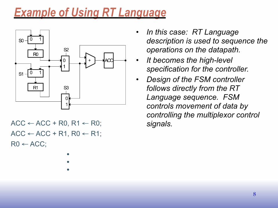
❑ Sometimes RT Language is used as a starting point for designing both the datapath and the control:
❑ example: regA ← IN; regB ← IN; regC ← regA + regB; regB ← regC; ❑ From this we can deduce:
– IN must fanout to both regA and regB – regA and regB must output to an adder – the adder must output to regC – regB must take its input from a mux
that selects between IN and regC
• What does the datapath look like:
• The controller:
9

EE141
List Processor Example
EE141
List Processor Example
❑ RT Language gives us a framework for making high-level optimizations.
❑ General design procedure outline: 1. Problem, Constraints, and Component Library Spec. 2. “Algorithm” Selection 3. Micro-architecture Specification 4. Analysis of Cost, Performance, Power 5. Optimizations, Variations 6. Detailed Design
11

EE141
1. Problem Specification
❑ Design a circuit that forms the sum of all the 2's complement integers stored in a linked-list structure starting at memory address 0:
❑ All integers and pointers are 8-bit. The link-list is stored in a memory block with an 8-bit address port and 8-bit data port, as shown below. The pointer from the last element in the list is 0. At least one node in list.
I/Os: – START resets to head of list
and starts addition process. – DONE signals completion – R holds the final result
Note: We don’t assume nodes are aligned on 2 Byte boundaries.12
EE141
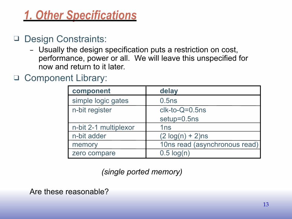
1. Other Specifications❑ Design Constraints:
– Usually the design specification puts a restriction on cost, performance, power or all. We will leave this unspecified for now and return to it later.
❑ Component Library: component delay simple logic gates 0.5ns n-bit register clk-to-Q=0.5ns setup=0.5ns n-bit 2-1 multiplexor 1ns n-bit adder (2 log(n) + 2)ns memory 10ns read (asynchronous read) zero compare 0.5 log(n)
(single ported memory)
Are these reasonable?13

EE141
Review of Register with “Clock Enable”
❑ Register with Clock Enable:
❑ Allows register to be either be loaded on selected clock posedge or to retain its previous value.
❑ Assume both data and CE require setup time = 0.5ns.
❑ Assume no reset input.
Functional description only. Transistor level circuit has lower input delay.
CE
CE
14
EE141
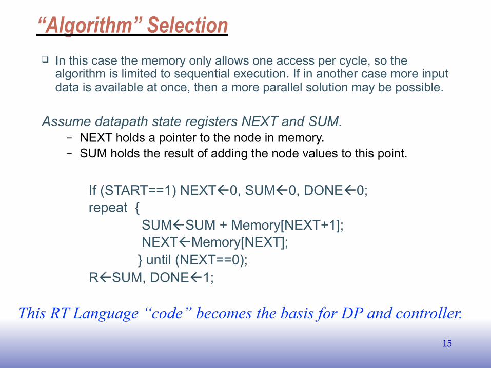
“Algorithm” Selection ❑ In this case the memory only allows one access per cycle, so the
algorithm is limited to sequential execution. If in another case more input data is available at once, then a more parallel solution may be possible.
Assume datapath state registers NEXT and SUM. – NEXT holds a pointer to the node in memory. – SUM holds the result of adding the node values to this point.
If (START==1) NEXTß0, SUMß0, DONEß0; repeat { SUMßSUM + Memory[NEXT+1]; NEXTßMemory[NEXT]; } until (NEXT==0); RßSUM, DONEß1;
This RT Language “code” becomes the basis for DP and controller.
15

EE141
3. Micro-Architecture #1Direct implementation of RTL description:
Datapath
Controller
If (START==1) NEXTß0, SUMß0; repeat { SUMßSUM + Memory[NEXT+1]; NEXTßMemory[NEXT]; } until (NEXT==0); RßSUM, DONEß1;
16

EE141
4. Analysis of Cost, Performance, and Power
❑ Skip Power for now. ❑ Cost:
– How do we measure it? # of transistors? # of gates? # of CLBs?
– Depends on implementation technology. Often we are just interested in comparing the relative cost of two competing implementations. (Save this for later)
❑ Performance: – 2 clock cycles per number added. – What is the minimum clock period? – The controller might be on the critical path. Therefore we
need to know the implementation, and controller input and output delay.
17

EE141
Possible Controller Implementation
❑ Based on this, what is the controller input and output delay?
18
One-hot FSM

EE141
4. Analysis of Performance
Other paths exist for each cycle in the loop. These are the worst case.
19

EE141
4. Analysis of Performance
❑ Detailed timing: clock period (T) = max (clock period for each state) T > 31ns, F < 32 MHz
❑ Observation: COMPUTE_SUM state does most of the work. Most of the
components are inactive in GET_NEXT state. GET_NEXT does: Memory access + … COMPUTE_SUM does: 8-bit add, memory access, 15-bit add + …
❑ Conclusion: Move one of the adds to GET_NEXT.
20

EE141
List Processor Optimization
EE141
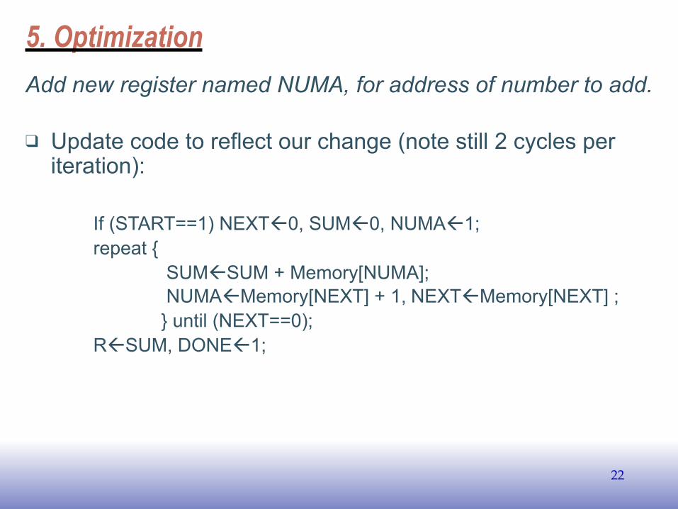
5. OptimizationAdd new register named NUMA, for address of number to add.
❑ Update code to reflect our change (note still 2 cycles per iteration):
If (START==1) NEXTß0, SUMß0, NUMAß1; repeat { SUMßSUM + Memory[NUMA]; NUMAßMemory[NEXT] + 1, NEXTßMemory[NEXT] ; } until (NEXT==0); RßSUM, DONEß1;
22

EE141
5. Optimization❑ Architecture #2:
❑ Incremental cost: addition of another register and mux.
If (START==1) NEXTß0, SUMß0, NUMAß1; repeat { SUMßSUM + Memory[NUMA]; NUMAßMemory[NEXT] + 1, NEXTßMemory[NEXT] ; } until (NEXT==0); RßSUM, DONEß1;
23

EE141
5. Optimization, Architecture #2
❑ New timing: Clock Period (T) = max (clock
period for each state)
T > 23ns, F < 43Mhz
❑ Is this worth the extra cost? ❑ Can we lower the cost?
Notice that the circuit now only performs one add on every cycle. Why not share the adder for both cycles?
24

EE141
5. Optimization, Architecture #3
❑ Incremental cost: – Addition of another mux and control (ADD_SEL). Removal of an 8-bit
adder. ❑ Performance:
– No change. ❑ Change is definitely worth it.
25

EE141
Resource Utilization Charts
EE141
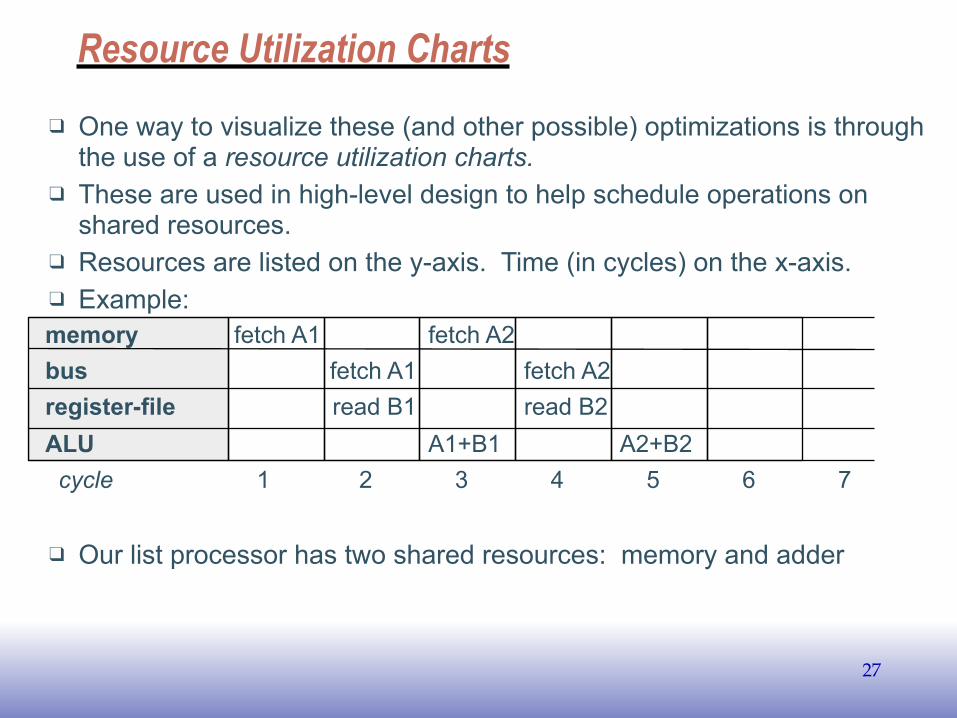
Resource Utilization Charts❑ One way to visualize these (and other possible) optimizations is through
the use of a resource utilization charts. ❑ These are used in high-level design to help schedule operations on
shared resources. ❑ Resources are listed on the y-axis. Time (in cycles) on the x-axis. ❑ Example: memory fetch A1 fetch A2 bus fetch A1 fetch A2 register-file read B1 read B2 ALU A1+B1 A2+B2 cycle 1 2 3 4 5 6 7
❑ Our list processor has two shared resources: memory and adder
27

EE141
List Example Resource Scheduling
❑ Unoptimized solution: 1. SUMßSUM + Memory[NEXT+1]; 2. NEXTßMemory[NEXT]; memory fetch x fetch next fetch x fetch next adder1 next+1 next+1 adder2 sum sum 1 2 1 2
• How about the other combination: add x register memory fetch x fetch next fetch x fetch next adder numa sum numa sum 1. XßMemory[NUMA], NUMAßNEXT+1; 2. NEXTßMemory[NEXT], SUMßSUM+X;
• Does this work? If so, a very short clock period. Each cycle could have independent fetch and add. T = max(Tmem, Tadd) instead of Tmem+ Tadd.
• Optimized solution: 1. SUMßSUM + Memory[NUMA]; 2. NEXTßMemory[NEXT], NUMAßMemory[NEXT]+1; memory fetch x fetch next fetch x fetch next adder sum numa sum numa
28

EE141
List Example Resource Scheduling
❑ Schedule one loop iteration followed by the next:
❑ How can we overlap iterations? next2 depends on next1. – “slide” second iteration into first (4 cycles per result):
– or further:
The repeating pattern is 4 cycles. Not exactly the pattern what we were looking for. But does it work correctly?
Memory next1 x1 next2 x2 adder numa1 sum1 numa2 sum2
Memory next1 x1 next2 x2 adder numa1 sum1 numa2 sum2
Memory next1 next2 x1 x2 next3 next4 x3 x4 adder numa1 numa2 sum1 sum2 numa3 numa4 sum3 sum4
29

EE141
List Example Resource Scheduling❑ In this case, first spread out, then pack.
1. XßMemory[NUMA], NUMAßNEXT+1; 2. NEXTßMemory[NEXT], SUMßSUM+X;
❑ Three different loop iterations active at once. ❑ Short cycle time (no dependencies within a cycle) ❑ full utilization (only 2 cycles per result) ❑ Initialization: x=0, numa=1, sum=0, next=memory[0] ❑ Control states (out of the loop)
– one to initialize next, clear sum, set numa, clear x – two to finish off after next==0.
Memory next1 x1 adder numa1 sum1
Memory next1 next2 x1 next3 x2 next4 x3 adder numa1 numa2 sum1 numa3 sum2 numa4 sum3
30

EE141
5. Optimization, Architecture #4
❑ Datapath:
❑ Incremental cost: – Addition of another register & mux, adder mux, and control.
❑ Performance: find max time of the four actions 1. XßMemory[NUMA], 0.5+1+10+1+0.5 = 13ns NUMAßNEXT+1; same for all ⇒ T>13ns, F<77MHz 2. NEXTßMemory[NEXT], SUMßSUM+X;
LD_NUMA
31
EE141
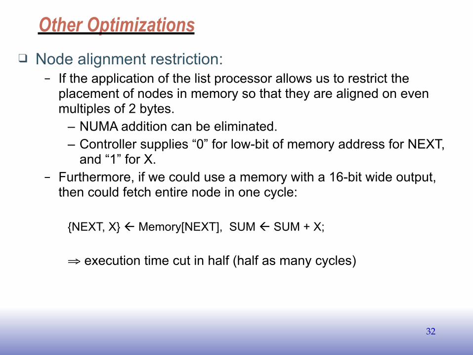
Other Optimizations❑ Node alignment restriction:
– If the application of the list processor allows us to restrict the placement of nodes in memory so that they are aligned on even multiples of 2 bytes.
– NUMA addition can be eliminated. – Controller supplies “0” for low-bit of memory address for NEXT,
and “1” for X. – Furthermore, if we could use a memory with a 16-bit wide output,
then could fetch entire node in one cycle:
{NEXT, X} ß Memory[NEXT], SUM ß SUM + X;
⇒ execution time cut in half (half as many cycles)
32
EE141
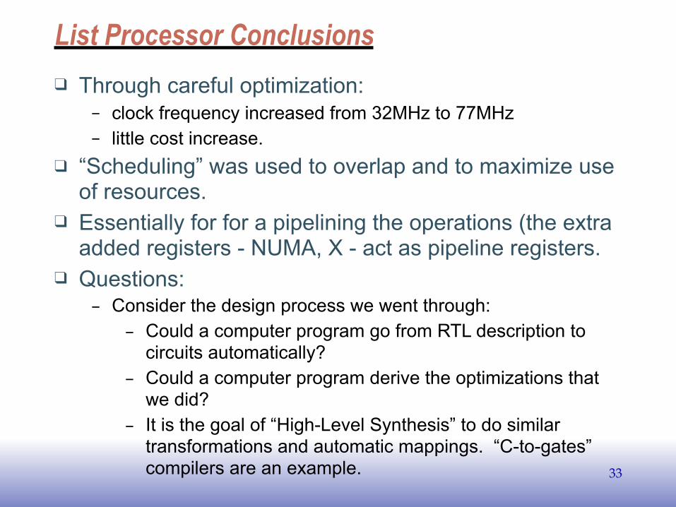
List Processor Conclusions❑ Through careful optimization:
– clock frequency increased from 32MHz to 77MHz – little cost increase.
❑ “Scheduling” was used to overlap and to maximize use of resources.
❑ Essentially for for a pipelining the operations (the extra added registers - NUMA, X - act as pipeline registers.
❑ Questions: – Consider the design process we went through:
– Could a computer program go from RTL description to circuits automatically?
– Could a computer program derive the optimizations that we did?
– It is the goal of “High-Level Synthesis” to do similar transformations and automatic mappings. “C-to-gates” compilers are an example. 33