Embed Size (px)
Citation preview
1
Fall 2011 EECS150 Lecture 2 Page 1
EECS150 - Digital DesignLecture 2 – Digital Logic and
FPGA Introduction
August 30, 2011
Elad AlonElectrical Engineering and Computer Sciences
University of California, Berkeley
http://www-inst.eecs.berkeley.edu/~cs150
Fall 2011 EECS150 Lecture 2 Page 2
Announcements• We have a new room!
– Starting this Thursday, lectures will be held in 9 Lewis
• Fri. discussion session shifted to 3-4pm– Mon. discussion still 11am-12pm
– First discussion this Friday
• Labs start today
• Homework #1 will be handed out later this week– Due next Thurs.
2
Fall 2011 EECS150 Lecture 2 Page 3
Digital Logic Review Outline• Topics in the review, you have already seen in CS61C,
and possibly EE40:1. Digital Signals.
2. General model for synchronous systems.
3. Combinational logic circuits
4. Flip-flops, clocking (Next lecture)
Fall 2011 EECS150 Lecture 2 Page 4
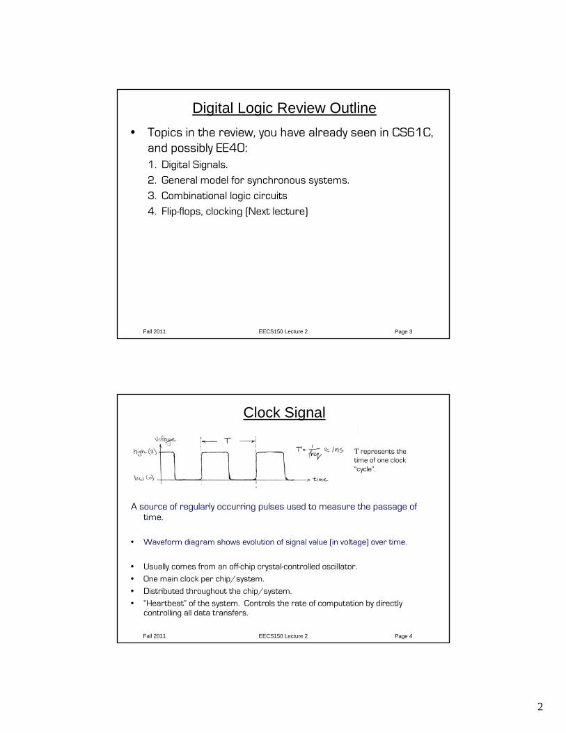
Clock Signal
A source of regularly occurring pulses used to measure the passage of time.
• Waveform diagram shows evolution of signal value (in voltage) over time.
• Usually comes from an off-chip crystal-controlled oscillator.
• One main clock per chip/system.
• Distributed throughout the chip/system.• “Heartbeat” of the system. Controls the rate of computation by directly
controlling all data transfers.
Τ represents the time of one clock “cycle”.
3
Fall 2011 EECS150 Lecture 2 Page 5
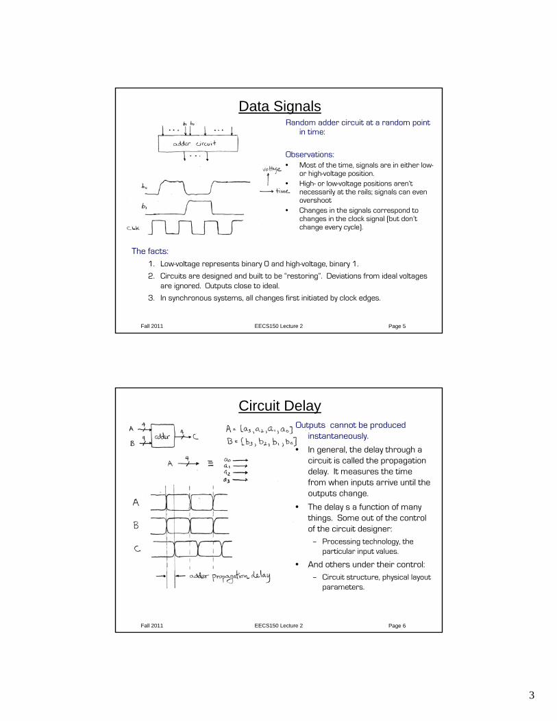
Data Signals
The facts:1. Low-voltage represents binary 0 and high-voltage, binary 1.
2. Circuits are designed and built to be “restoring”. Deviations from ideal voltages are ignored. Outputs close to ideal.
3. In synchronous systems, all changes first initiated by clock edges.
Random adder circuit at a random point in time:
Observations:• Most of the time, signals are in either low-
or high-voltage position.• High- or low-voltage positions aren’t
necessarily at the rails; signals can even overshoot
• Changes in the signals correspond to changes in the clock signal (but don’t change every cycle).
Fall 2011 EECS150 Lecture 2 Page 6
Circuit DelayOutputs cannot be produced
instantaneously.
• In general, the delay through a circuit is called the propagation delay. It measures the time from when inputs arrive until the outputs change.
• The delay s a function of many things. Some out of the control of the circuit designer:
– Processing technology, the particular input values.
• And others under their control:– Circuit structure, physical layout
parameters.
4
Fall 2011 EECS150 Lecture 2 Page 7
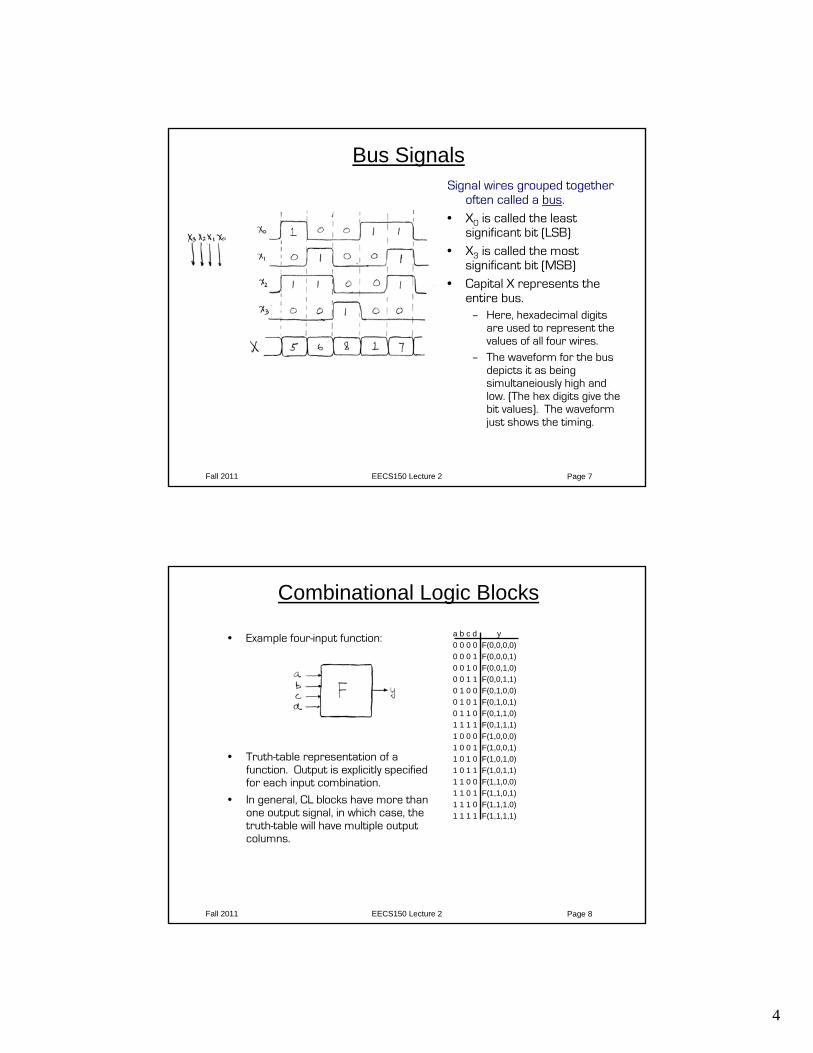
Bus SignalsSignal wires grouped together
often called a bus.• X0 is called the least
significant bit (LSB)• X3 is called the most
significant bit (MSB)• Capital X represents the
entire bus.– Here, hexadecimal digits
are used to represent the values of all four wires.
– The waveform for the bus depicts it as being simultaneiously high and low. (The hex digits give the bit values). The waveform just shows the timing.
Fall 2011 EECS150 Lecture 2 Page 8
Combinational Logic Blocks
• Example four-input function:
• Truth-table representation of a function. Output is explicitly specified for each input combination.
• In general, CL blocks have more than one output signal, in which case, the truth-table will have multiple output columns.
a b c d y0 0 0 0 F(0,0,0,0)0 0 0 1 F(0,0,0,1)0 0 1 0 F(0,0,1,0)0 0 1 1 F(0,0,1,1)0 1 0 0 F(0,1,0,0)0 1 0 1 F(0,1,0,1)0 1 1 0 F(0,1,1,0)1 1 1 1 F(0,1,1,1)1 0 0 0 F(1,0,0,0)1 0 0 1 F(1,0,0,1)1 0 1 0 F(1,0,1,0)1 0 1 1 F(1,0,1,1)1 1 0 0 F(1,1,0,0)1 1 0 1 F(1,1,0,1)1 1 1 0 F(1,1,1,0)1 1 1 1 F(1,1,1,1)
5
Fall 2011 EECS150 Lecture 2 Page 9
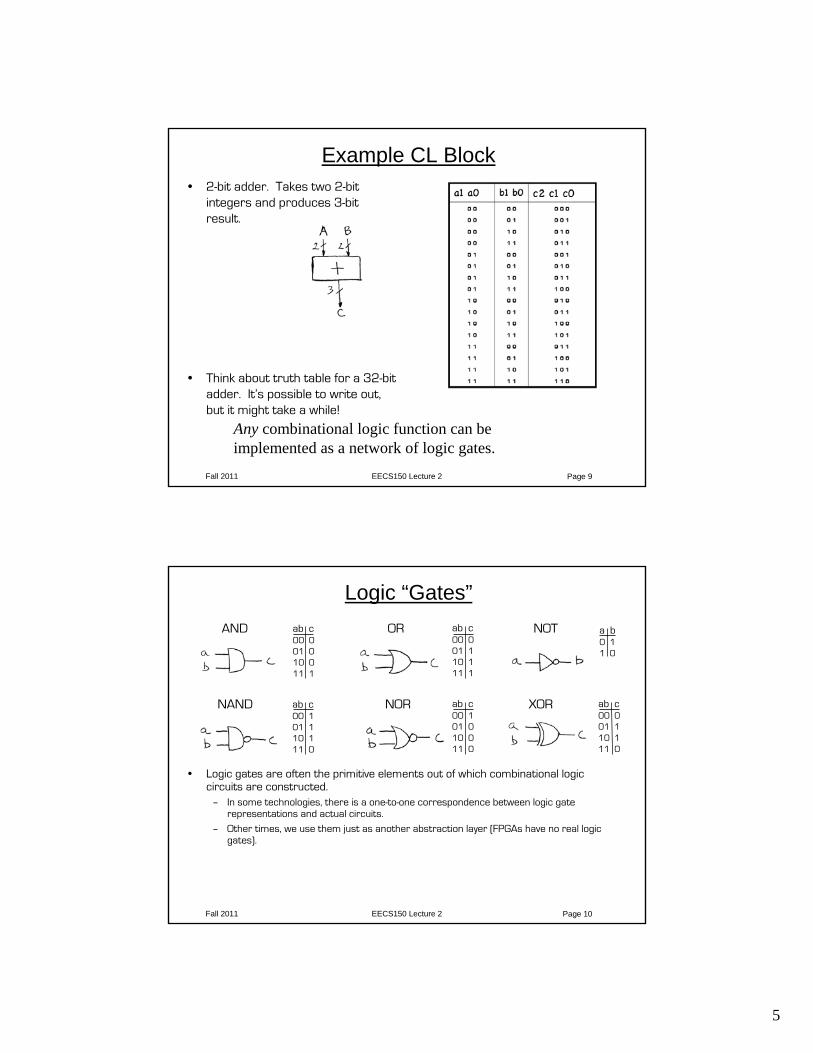
Example CL Block• 2-bit adder. Takes two 2-bit
integers and produces 3-bit result.
• Think about truth table for a 32-bit adder. It’s possible to write out, but it might take a while!
Any combinational logic function can be implemented as a network of logic gates.
Fall 2011 EECS150 Lecture 2 Page 10
Logic “Gates”ab c00 001 010 011 1
AND ab c00 001 110 111 1
OR NOT a b0 11 0
ab c00 101 110 111 0
NAND ab c00 101 010 011 0
NOR ab c00 001 110 111 0
XOR
• Logic gates are often the primitive elements out of which combinational logic circuits are constructed.
– In some technologies, there is a one-to-one correspondence between logic gate representations and actual circuits.
– Other times, we use them just as another abstraction layer (FPGAs have no real logic gates).
6
Fall 2011 EECS150 Lecture 2 Page 11
What Makes a Circuit Digital?
Fall 2011 EECS150 Lecture 2 Page 12
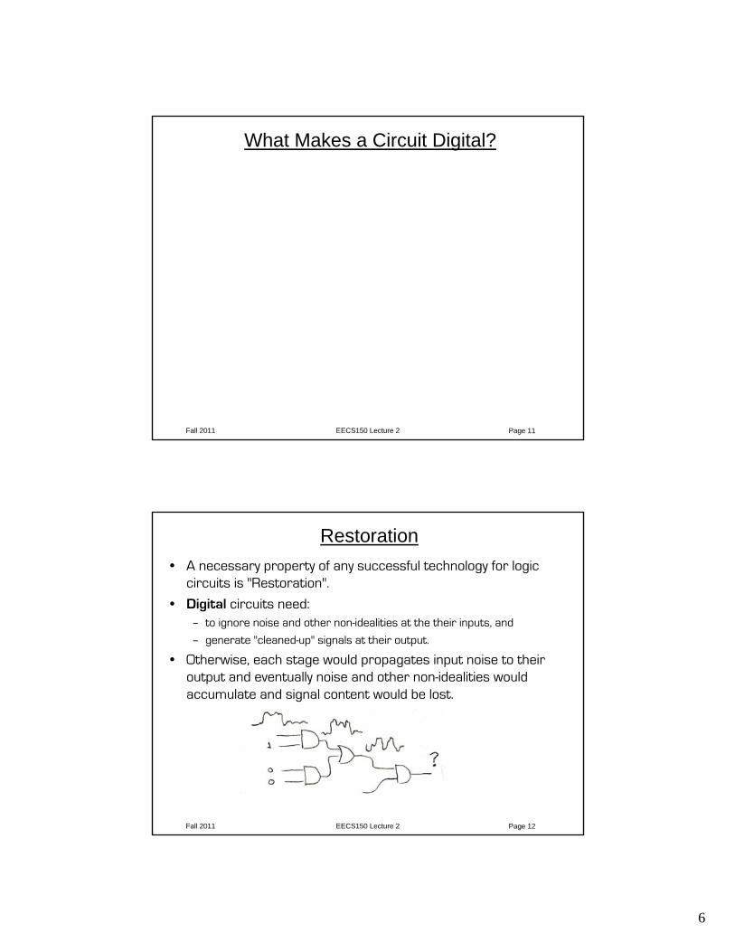
Restoration• A necessary property of any successful technology for logic
circuits is "Restoration".
• Digital circuits need:– to ignore noise and other non-idealities at the their inputs, and
– generate "cleaned-up" signals at their output.
• Otherwise, each stage would propagates input noise to their output and eventually noise and other non-idealities would accumulate and signal content would be lost.
7
Fall 2011 EECS150 Lecture 2 Page 13
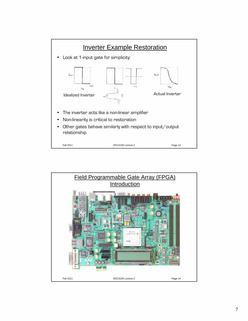
Inverter Example Restoration• Look at 1-input gate for simplicity:
• The inverter acts like a non-linear amplifier
• Non-linearity is critical to restoration
• Other gates behave similarly with respect to input/output relationship
Idealized Inverter Actual Inverter
Fall 2011 EECS150 Lecture 2 Page 14
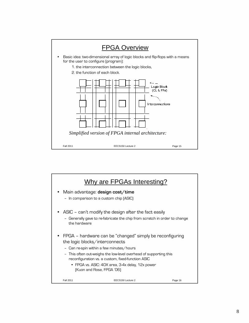
Field Programmable Gate Array (FPGA) Introduction
8
Fall 2011 EECS150 Lecture 2 Page 15
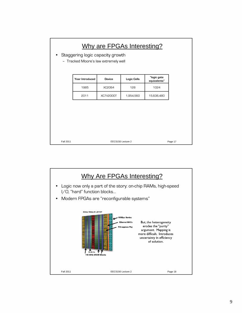
FPGA Overview• Basic idea: two-dimensional array of logic blocks and flip-flops with a means
for the user to configure (program):1. the interconnection between the logic blocks,2. the function of each block.
Simplified version of FPGA internal architecture:
Fall 2011 EECS150 Lecture 2 Page 16
Why are FPGAs Interesting?• Main advantage: design cost/time
– In comparison to a custom chip (ASIC)
• ASIC – can’t modify the design after the fact easily– Generally gave to re-fabricate the chip from scratch in order to change
the hardware
• FPGA – hardware can be “changed” simply be reconfiguring the logic blocks/interconnects– Can re-spin within a few minutes/hours
– This often out-weighs the low-level overhead of supporting this reconfiguration vs. a custom, fixed-function ASIC
• FPGA vs. ASIC: 40X area, 3-4x delay, 12x power (Kuon and Rose, FPGA ’06)
9
Fall 2011 EECS150 Lecture 2 Page 17
Why are FPGAs Interesting?
Year Introduced Device Logic Cells“logic gate
equivalents”
1985 XC2064 128 1024
2011 XC7V2000T 1,954,560 15,636,480
• Staggering logic capacity growth– Tracked Moore’s law extremely well
Fall 2011 EECS150 Lecture 2 Page 18
Why Are FPGAs Interesting?• Logic now only a part of the story: on-chip RAMs, high-speed
I/O, “hard” function blocks…
• Modern FPGAs are “reconfigurable systems”
10
Fall 2011 EECS150 Lecture 2 Page 19
Background (review) for upcoming• A MUX or multiplexor is a combinational logic circuit that
chooses between 2N inputs under the control of N control signals.
• A latch is a 1-bit memory (similar to a flip-flop).
Fall 2011 EECS150 Lecture 2 Page 20
FPGA Variations• Families of FPGA’s differ in:
– physical means of implementing user programmability,
– arrangement of interconnection wires, and
– the basic functionality of the logic blocks.
• Most significant difference is in the method for providing flexible blocks and connections:
• Anti-fuse based (ex: Actel)
+ Non-volatile, relatively small
– fixed (non-reprogrammable)
• Several “floating gate” or eprom style approaches have been used. One now by Actel.
11
Fall 2011 EECS150 Lecture 2 Page 21
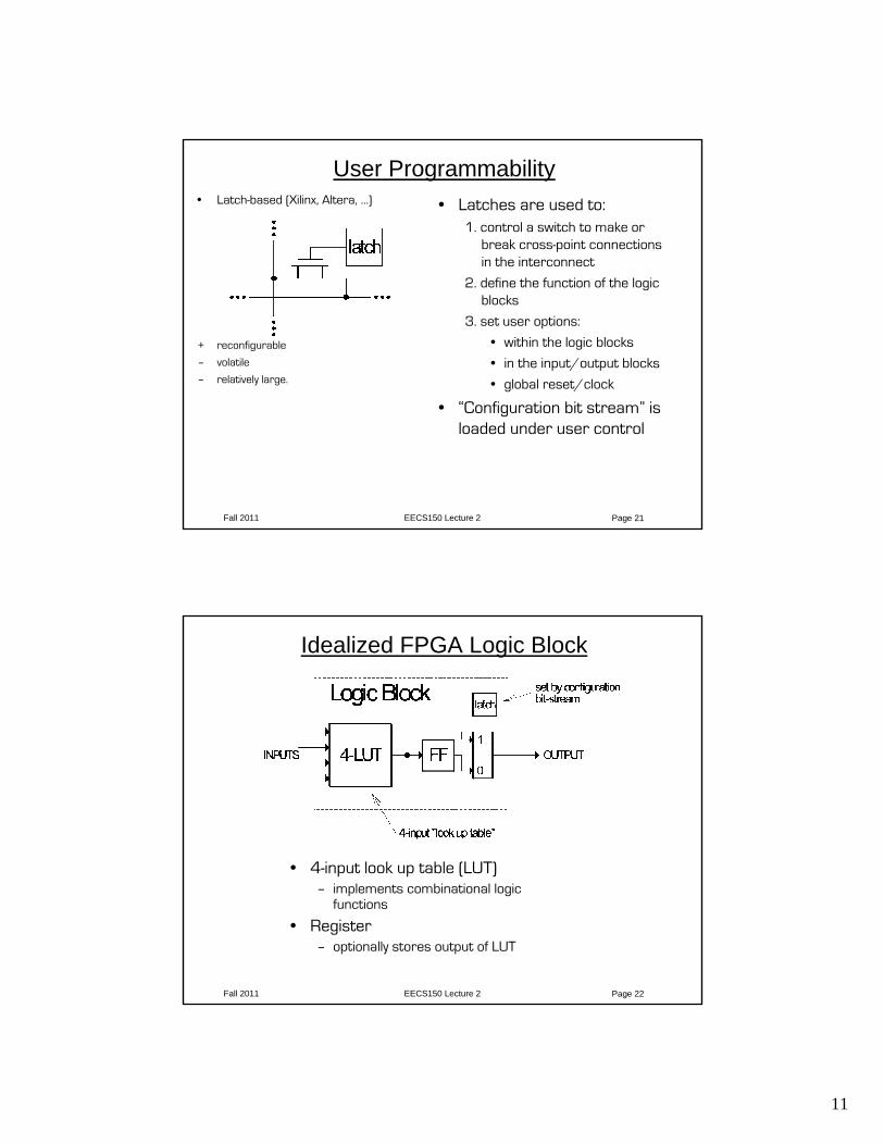
User Programmability• Latches are used to:
1. control a switch to make or break cross-point connections in the interconnect
2. define the function of the logic blocks
3. set user options:
• within the logic blocks
• in the input/output blocks
• global reset/clock
• “Configuration bit stream” is loaded under user control
• Latch-based (Xilinx, Altera, …)
+ reconfigurable
– volatile
– relatively large.
Fall 2011 EECS150 Lecture 2 Page 22
Idealized FPGA Logic Block
• 4-input look up table (LUT)– implements combinational logic
functions
• Register– optionally stores output of LUT
12
Fall 2011 EECS150 Lecture 2 Page 23
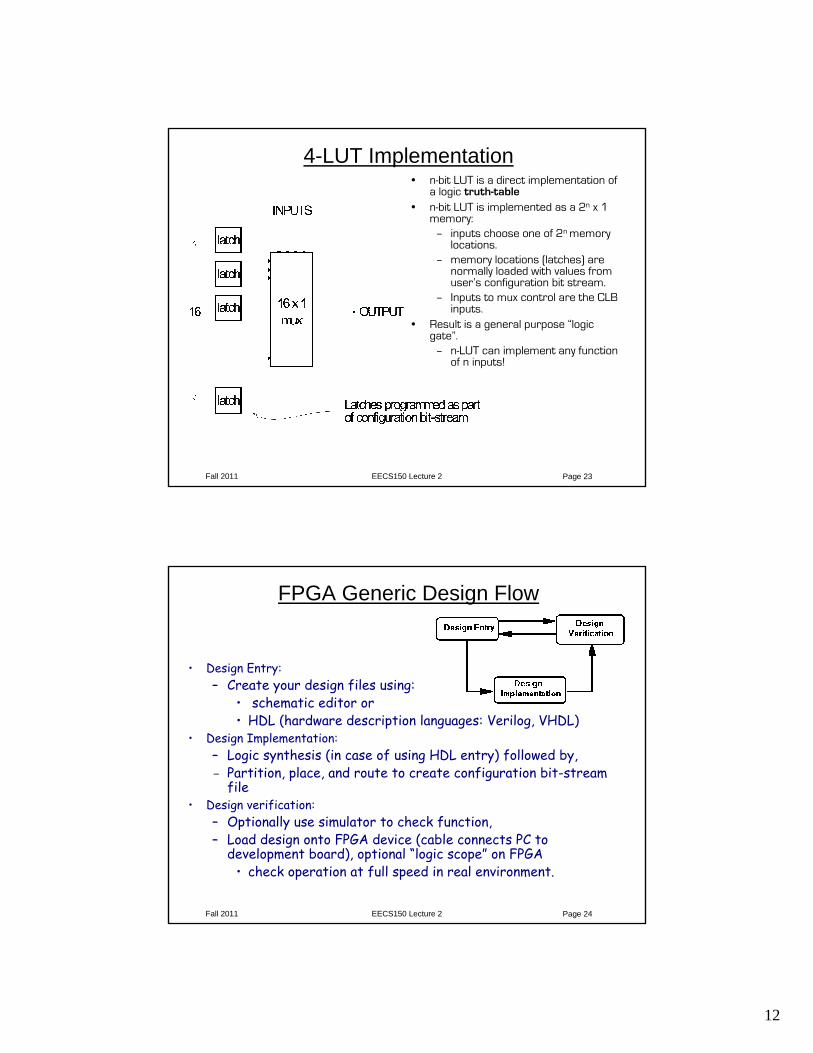
4-LUT Implementation• n-bit LUT is a direct implementation of
a logic truth-table• n-bit LUT is implemented as a 2n x 1
memory:– inputs choose one of 2n memory
locations.– memory locations (latches) are
normally loaded with values from user’s configuration bit stream.
– Inputs to mux control are the CLB inputs.
• Result is a general purpose “logic gate”. – n-LUT can implement any function
of n inputs!
Fall 2011 EECS150 Lecture 2 Page 24
FPGA Generic Design Flow
• Design Entry:– Create your design files using:
• schematic editor or • HDL (hardware description languages: Verilog, VHDL)
• Design Implementation:– Logic synthesis (in case of using HDL entry) followed by,– Partition, place, and route to create configuration bit-stream
file• Design verification:
– Optionally use simulator to check function,– Load design onto FPGA device (cable connects PC to
development board), optional “logic scope” on FPGA• check operation at full speed in real environment.
13
Fall 2011 EECS150 Lecture 2 Page 25
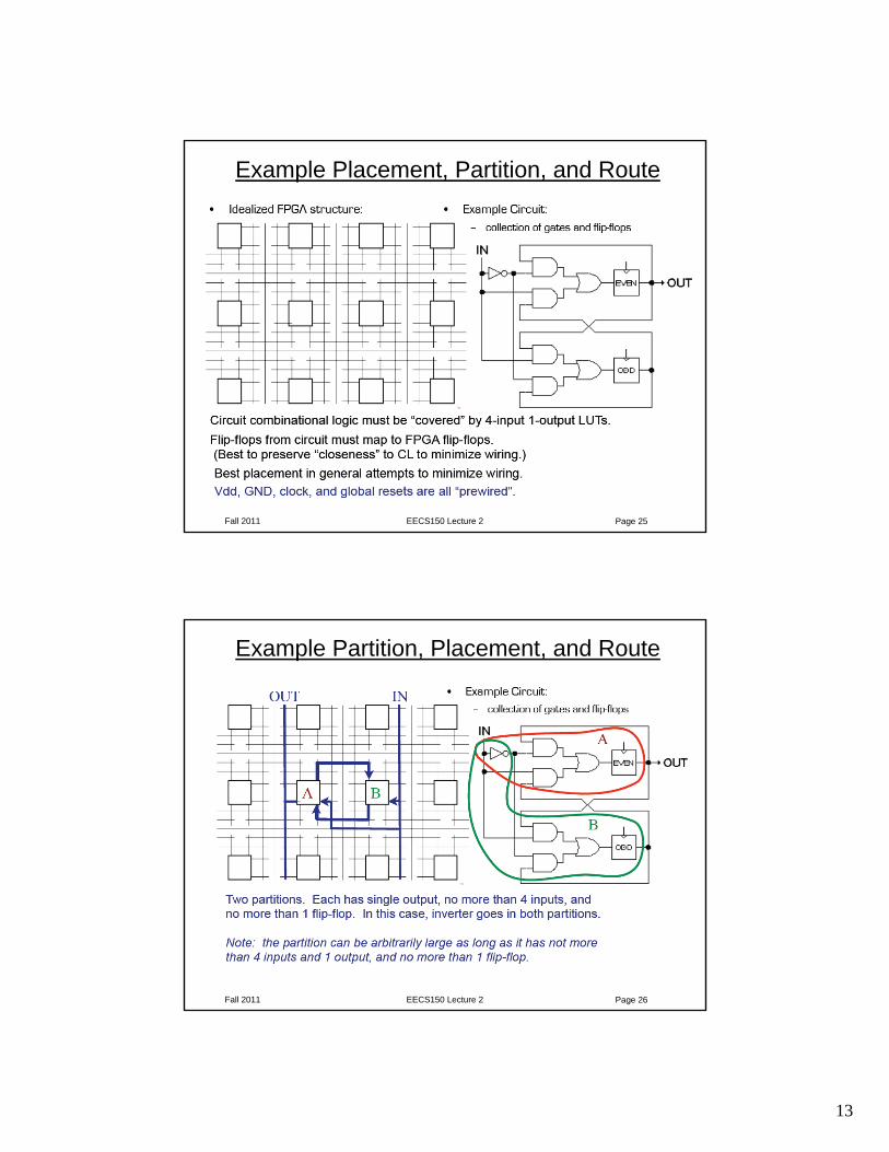
Example Placement, Partition, and Route
Fall 2011 EECS150 Lecture 2 Page 26
Example Partition, Placement, and Route
14
Fall 2011 EECS150 Lecture 2 Page 27
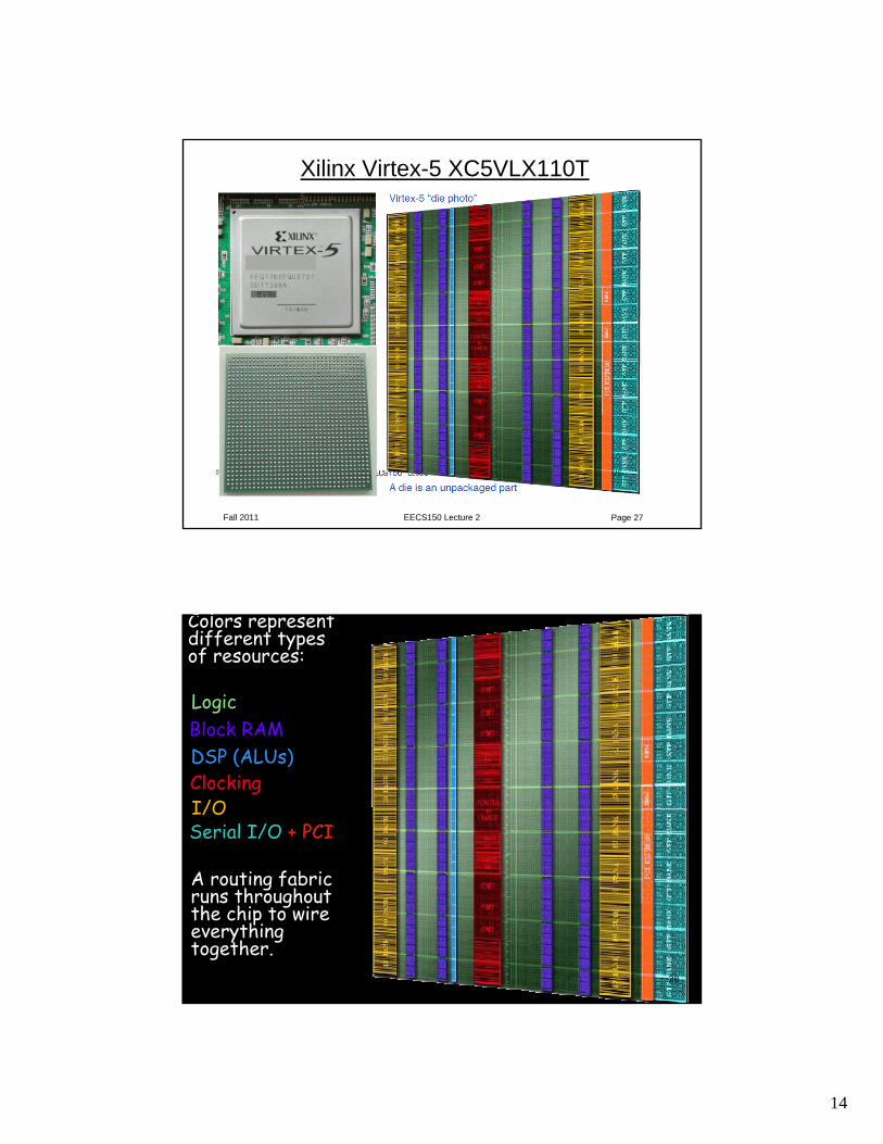
Xilinx Virtex-5 XC5VLX110T
Fall 2011 EECS150 Lecture 2 Page 28
Spring 2011 EECS150 - Lec03-FPGA Page
Colors represent different types of resources:
LogicBlock RAMDSP (ALUs)ClockingI/OSerial I/O + PCI
A routing fabric runs throughout the chip to wire everything together.
28
15
Fall 2011 EECS150 Lecture 2 Page 29
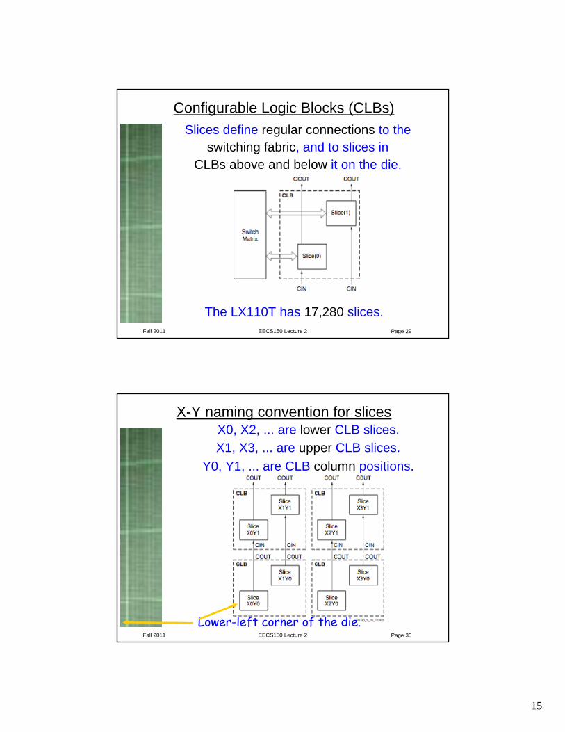
Configurable Logic Blocks (CLBs)Slices define regular connections to the
switching fabric, and to slices in CLBs above and below it on the die.
The LX110T has 17,280 slices.
Fall 2011 EECS150 Lecture 2 Page 30
X-Y naming convention for slices
Lower-left corner of the die.
X0, X2, ... are lower CLB slices.X1, X3, ... are upper CLB slices.
Y0, Y1, ... are CLB column positions.
16
Fall 2011 EECS150 Lecture 2 Page 31
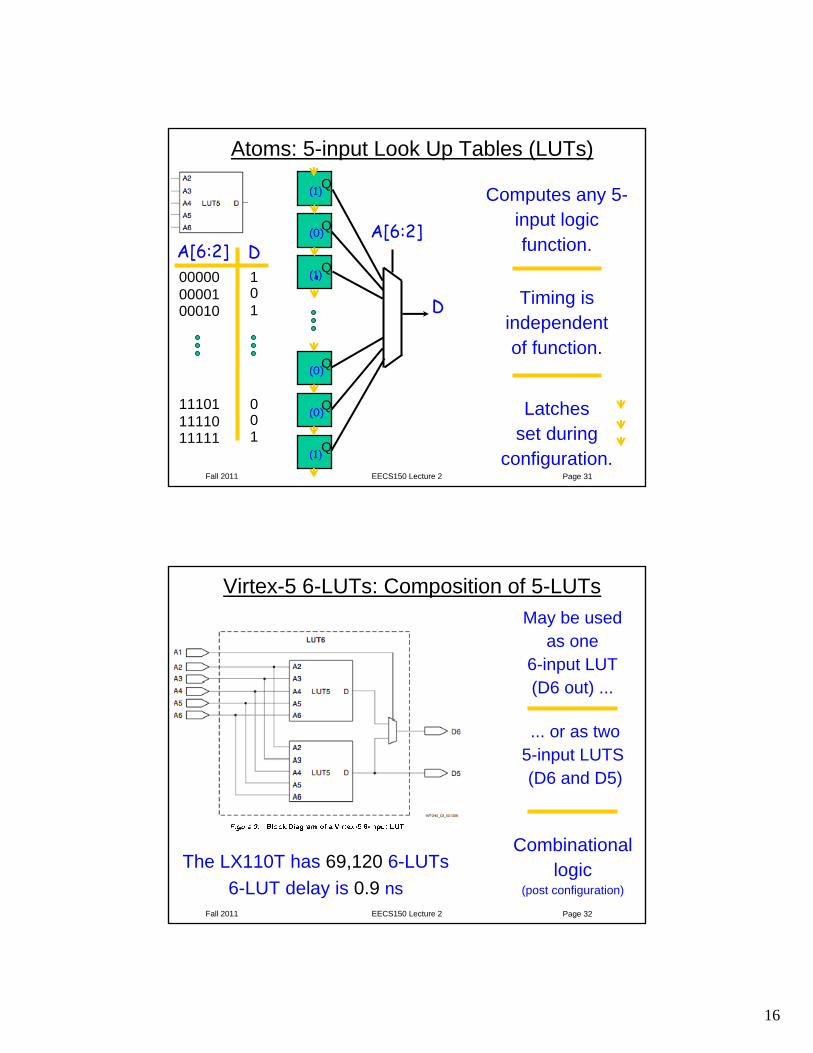
Atoms: 5-input Look Up Tables (LUTs)
A[6:2] D000000000100010
101
111011111011111
001
Q
Q
Q
Q
Q
Q
(1)
(1)
(1)
(0)
(0)
(0)
....D
A[6:2]
Computes any 5-input logic function.
Timing is independent of function.
Latchesset during
configuration.
Fall 2011 EECS150 Lecture 2 Page 32
Virtex-5 6-LUTs: Composition of 5-LUTsMay be used
as one 6-input LUT (D6 out) ...
Combinational logic
(post configuration)
... or as two 5-input LUTS(D6 and D5)
The LX110T has 69,120 6-LUTs6-LUT delay is 0.9 ns
17
Fall 2011 EECS150 Lecture 2 Page 33
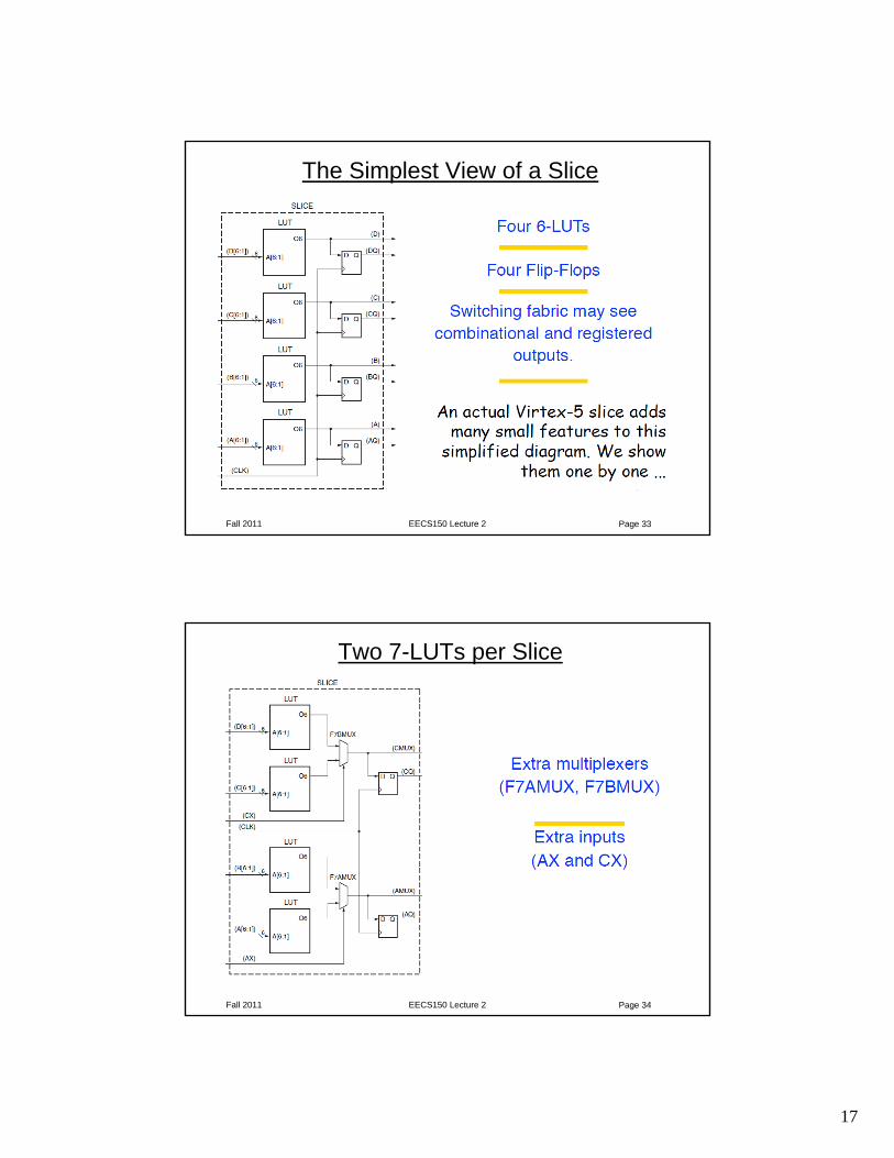
The Simplest View of a Slice
Fall 2011 EECS150 Lecture 2 Page 34
Two 7-LUTs per Slice
18
Fall 2011 EECS150 Lecture 2 Page 35
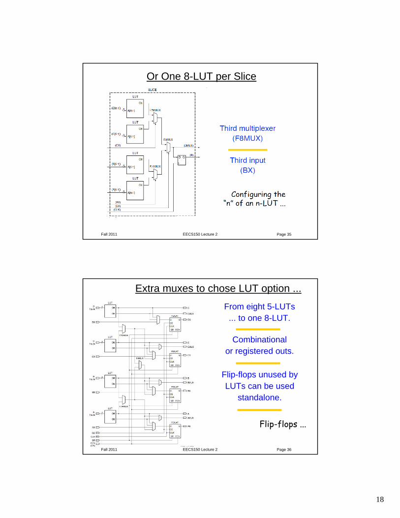
Or One 8-LUT per Slice
Fall 2011 EECS150 Lecture 2 Page 36
Extra muxes to chose LUT option ...
From eight 5-LUTs ... to one 8-LUT.
Combinational or registered outs.
Flip-flops unused by LUTs can be used
standalone.
Flip-flops ...
19
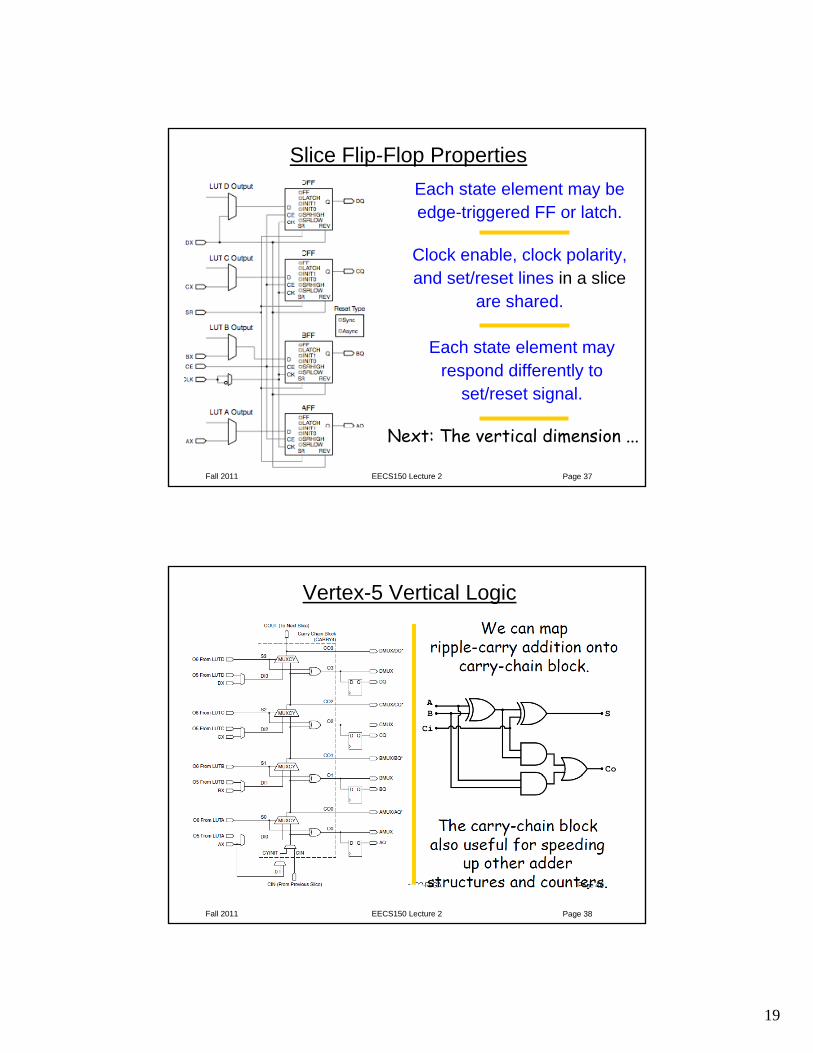
Fall 2011 EECS150 Lecture 2 Page 37
Slice Flip-Flop PropertiesEach state element may be edge-triggered FF or latch.
Each state element may respond differently to
set/reset signal.
Clock enable, clock polarity, and set/reset lines in a slice
are shared.
Next: The vertical dimension ...
Fall 2011 EECS150 Lecture 2 Page 38
Vertex-5 Vertical Logic
20
Fall 2011 EECS150 Lecture 2 Page 39
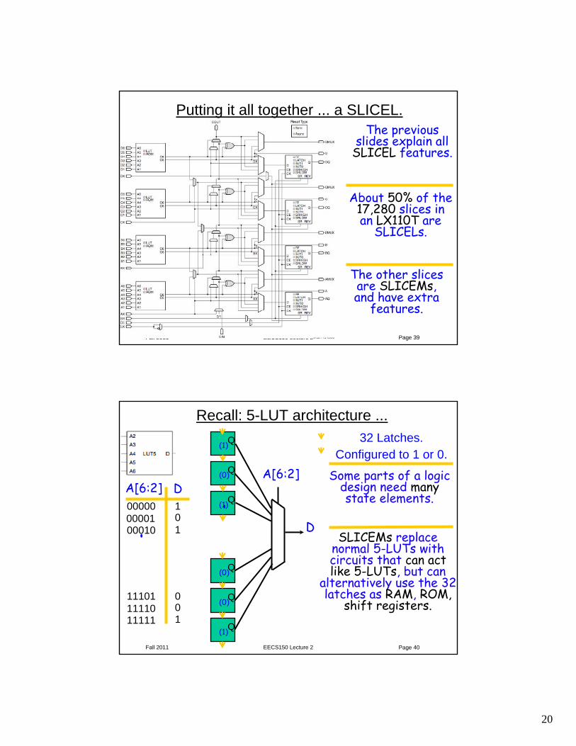
Putting it all together ... a SLICEL.The previous
slides explain all SLICEL features.
About 50% of the 17,280 slices in an LX110T are
SLICELs.
The other slices are SLICEMs, and have extra
features.
Fall 2011 EECS150 Lecture 2 Page 40
Recall: 5-LUT architecture ...
A[6:2] D000000000100010....
101
111011111011111
001
Q
Q
Q
Q
Q
Q
(1)
(1)
(1)
(0)
(0)
(0)
....D
A[6:2]
32 Latches. Configured to 1 or 0.
Some parts of a logic design need manystate elements.
SLICEMs replace normal 5-LUTs with circuits that can act like 5-LUTs, but can
alternatively use the 32 latches as RAM, ROM,
shift registers.
21
Fall 2011 EECS150 Lecture 2 Page 41
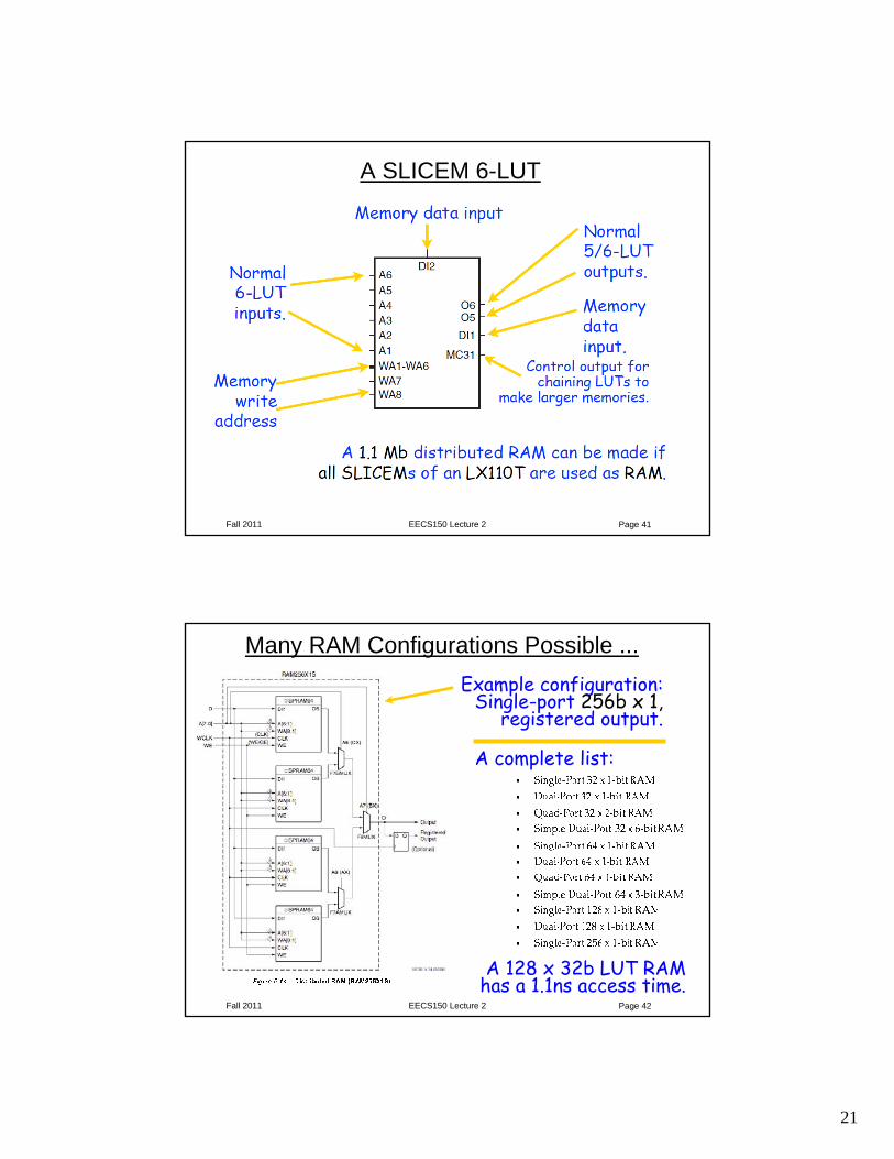
A SLICEM 6-LUT
Fall 2011 EECS150 Lecture 2 Page 42
Many RAM Configurations Possible ...Example configuration:
Single-port 256b x 1,registered output.
A complete list:
A 128 x 32b LUT RAM has a 1.1ns access time.
22
Fall 2011 EECS150 Lecture 2 Page 43
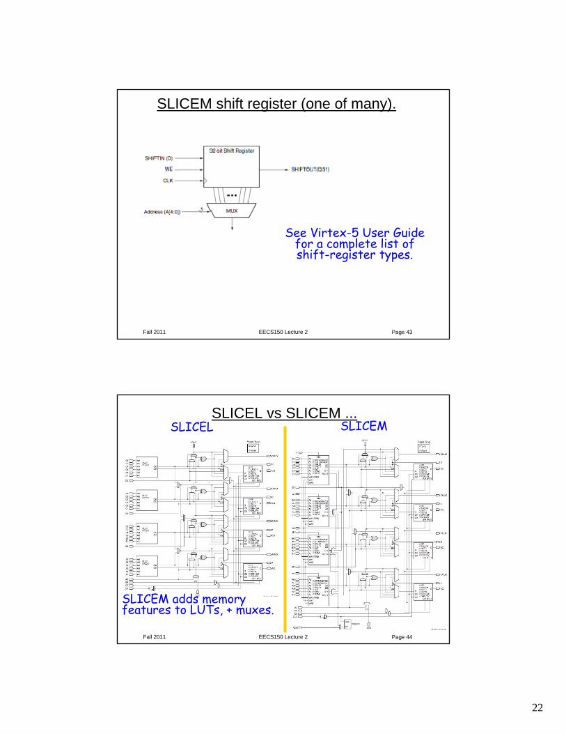
SLICEM shift register (one of many).
See Virtex-5 User Guide for a complete list of shift-register types.
Fall 2011 EECS150 Lecture 2 Page 44
SLICEL vs SLICEM ...SLICEMSLICEL
SLICEM adds memory features to LUTs, + muxes.
23
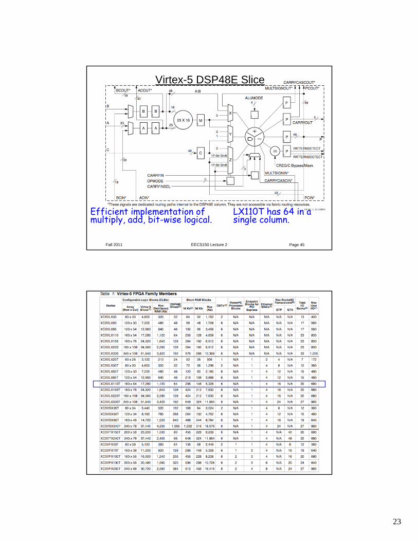
Fall 2011 EECS150 Lecture 2 Page 45
Virtex-5 DSP48E Slice
Efficient implementation of multiply, add, bit-wise logical.
LX110T has 64 in a single column.
Fall 2011 EECS150 Lecture 2 Page 46
24
Fall 2011 EECS150 Lecture 2 Page 47
Spring 2011 EECS150 - Lec03-FPGA Page
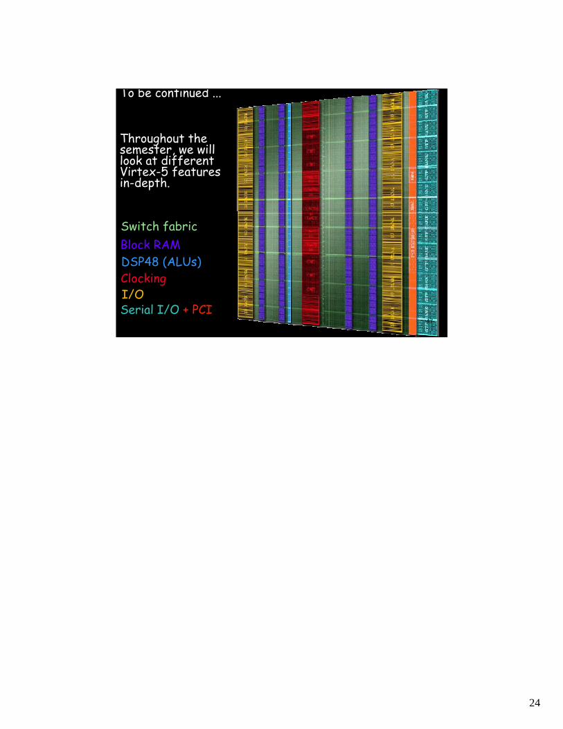
To be continued ...
Throughout the semester, we will look at different Virtex-5 features in-depth.
Switch fabricBlock RAMDSP48 (ALUs)ClockingI/OSerial I/O + PCI
47