Embed Size (px)
Citation preview

Spring 2003 EECS150 - Lec16-mem1 Page 1
EECS150 - Digital DesignLecture 16 – Memory 1
March 13, 2003John Wawrzynek

Spring 2003 EECS150 - Lec16-mem1 Page 2
Memory Basics• Uses:
Whenever a large collection of state elements is required.
– data & program storage – general purpose registers – buffering – table lookups – CL implementation
• Types:– RAM - random access memory – ROM - read only memory – EPROM, FLASH - electrically
programmable read only memory
• Example RAM: Register file from microprocessor
regid = register identifier (address of word in memory)sizeof(regid) = log2(# of reg) WE = write enable
clk

Spring 2003 EECS150 - Lec16-mem1 Page 3
Definitions
Memory Interfaces for Accessing Data• Asynchronous (unclocked):
A change in the address results in data appearing • Synchronous (clocked):
A change in address, followed by an edge on CLK results in data appearing or write operation occurring.
A common arrangement is to have synchronous write operations andasynchronous read operations.
• Volatile:Looses its state when the power goes off.
• Nonvolatile:Retains it state when power goes off.

Spring 2003 EECS150 - Lec16-mem1 Page 4
Register File Internals• For read operations,
functionally the regfile is equivalent to a 2-D array of flip-flops with tristateoutputs on each:
• Cell with added write logic:
How do we go from "regid" to "SEL"?
These circuits are just functional abstractions of the actual circuits used.

Spring 2003 EECS150 - Lec16-mem1 Page 5
Regid (address) Decoding
• The function of the address decoder is to generate a one-hot code word from the address.
• The output is use for row selection.• Many different circuits exist for this
function. A simple one is shown to the right.

Spring 2003 EECS150 - Lec16-mem1 Page 6
Standard Internal Memory Organization
• Special circuit tricks are used for the cell array to improve storage density. (We will look at these later)
• RAM/ROM naming convention: – examples: 32 X 8, "32 by 8" => 32 8-bit words – 1M X 1, "1 meg by 1" => 1M 1-bit words
2-D arrary of bit cells. Each cell stores one bit of data.

Spring 2003 EECS150 - Lec16-mem1 Page 7
Read Only Memory (ROM)• Simply for of memory. No write operation needed.• Functional Equivalence:
• Full tri-state buffers are not needed at each cell point.• In practice, single transistors are used to implement zero cells. Logic
one’s are derived through precharging or bit-line pullup transistor.
Connections to Vdd used to store a logic 1, connections to GND for storing logic 0.
address decoder bit-cell array

Spring 2003 EECS150 - Lec16-mem1 Page 8
Column MUX in ROMs and RAMs: • Controls physical aspect ratio
– Important for physical layout and to control delay on wires.• In DRAM, allows time-multiplexing of chip address pins

Spring 2003 EECS150 - Lec16-mem1 Page 9
Cascading Memory Modules (or chips) • Example: assemblage of 256 x 8
ROM using 256 x 4 modules:
• example: 1K x * ROM using 256 x 4 modules:
• each module has tri-state outputs:

Spring 2003 EECS150 - Lec16-mem1 Page 10
Memory Components Types:• Volatile:
– Random Access Memory (RAM): • DRAM "dynamic" • SRAM "static"
• Non-volatile:– Read Only Memory (ROM):
• Mask ROM "mask programmable" • EPROM "electrically programmable" • EEPROM "erasable electrically programmable" • FLASH memory - similar to EEPROM with programmer
integrated on chip

Spring 2003 EECS150 - Lec16-mem1 Page 11
Volatile Memory Comparison
• SRAM Cell
• Larger cell ⇒ lower density, higher cost/bit
• No refresh required
• Simple read ⇒ faster access • Standard IC process ⇒ natural for
integration with logic
• DRAM Cell
• Smaller cell ⇒ higher density, lower cost/bit
• Needs periodic refresh, and refresh after read
• Complex read ⇒ longer access time • Special IC process ⇒ difficult to
integrate with logic circuits
word line
bit line bit line
word line
bit line
The primary difference between different memory types is the bit cell.

Spring 2003 EECS150 - Lec16-mem1 Page 12
Multi-ported Memory• Motivation:
– Consider CPU core register file:• 1 read or write per cycle limits
processor performance.• Complicates pipelining. Difficult
for different instructions to simultaneously read or write regfile.
• Common arrangement in pipelined CPUs is 2 read ports and 1 write port.
databuffer
disk/network
CPU
• Motivation:– I/O data buffering:
• dual-porting allows both sides to simultaneously access memory at full bandwidth.
addradataaRWa
addrbdatabRWb
Dual-portMemorysela
selbselc
dataa
datab datac
Regfile
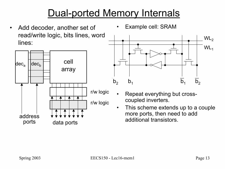
Spring 2003 EECS150 - Lec16-mem1 Page 13
Dual-ported Memory Internals• Add decoder, another set of
read/write logic, bits lines, word lines:
• Example cell: SRAM
• Repeat everything but cross-coupled inverters.
• This scheme extends up to a couple more ports, then need to add additional transistors.
deca decbcell
array
r/w logic
r/w logic
data portsaddress
ports
b2 b2b1 b1
WL2
WL1

Spring 2003 EECS150 - Lec16-mem1 Page 14
Memory in Desktop Computer Systems:
• SRAM (lower density, higher speed) used in CPU register file, on- and off-chip caches.
• DRAM (higher density, lower speed) used in main memory
Closing the GAP: 1. Caches are growing in size.2. Innovation targeted towards higher bandwidth for memory systems:
– SDRAM - synchronous DRAM – RDRAM - Rambus DRAM – EDORAM - extended data out SRAM – Three-dimensional RAM – hyper-page mode DRAM video RAM – multibank DRAM

Spring 2003 EECS150 - Lec16-mem1 Page 15
Important DRAM Examples:• EDO - extended data out (similar to fast-page mode)
– RAS cycle fetched rows of data from cell array blocks (long access time, around 100ns)
– Subsequent CAS cycles quickly access data from row buffers if within an address page (page is around 256 Bytes)
• SDRAM - synchronous DRAM– clocked interface – uses dual banks internally. Start access in one back then next, then
receive data from first then second. • DDR - Double data rate SDRAM
– Uses both rising (positive edge) and falling (negative) edge of clock for data transfer. (typical 100MHz clock with 200 MHz transfer).
• RDRAM - Rambus DRAM – Entire data blocks are access and transferred out on a highspeed bus-like
interface (500 MB/s, 1.6 GB/s) – Tricky system level design. More expensive memory chips.

Spring 2003 EECS150 - Lec16-mem1 Page 16
Non-volatile Memory
• Mask ROM – Used with logic circuits for tables etc.– Contents fixed at IC fab time (truly write once!)
• EPROM (erasable programmable)& FLASH – requires special IC process
(floating gate technology)
– writing is slower than RAM. EPROM uses special programming system to provide special voltages and timing.
– reading can be made fairly fast.– rewriting is very slow.
• erasure is first required , EPROM - UV light exposure, EEPROM –electrically erasable
Used to hold fixed code (ex. BIOS), tables of data (ex. FSM next state/output logic), slowly changing values (date/time on computer)

Spring 2003 EECS150 - Lec16-mem1 Page 17
FLASH Memory • Electrically erasable • In system programmability and erasability (no special system or
voltages needed) • On-chip circuitry (FSM) and voltage generators to control erasure and
programming (writing) • Erasure happens in variable sized "sectors" in a flash (16K - 64K
Bytes)
• Compact flash cards are based on this type of memory.
See: http://developer.intel.com/design/flash/for product descriptions, etc.

Spring 2003 EECS150 - Lec16-mem1 Page 18
Memory Specification in Verilog• Memory modeled by an array of registers:
reg[15:0] memword[0:1023]; // 1,024 registers of 16 bits each
//Example Memory Block Specification// Uses enable to control both write and read//-----------------------------//Read and write operations of memory.//Memory size is 64 words of 4 bits each. module memory (Enable,ReadWrite,Address,DataIn,DataOut);
input Enable,ReadWrite;input [3:0] DataIn;input [5:0] Address;output [3:0] DataOut;reg [3:0] DataOut;reg [3:0] Mem [0:63]; //64 x 4 memoryalways @ (Enable or ReadWrite)
if (Enable)if (ReadWrite)
DataOut = Mem[Address]; //Readelse
Mem[Address] = DataIn; //Writeelse DataOut = 4'bz; //High impedance state
endmodule

Spring 2003 EECS150 - Lec16-mem1 Page 19
Memory Blocks in FPGAs• LUTs can double as small RAM blocks:
– 4-LUT is really a 16x1 memory. Normally we think of the contents being written from the configuration bit stream, but Virtex architecture (and others) allow bits of LUT to be written and read from the general interconnect structure.
– achieves 16x density advantage over using CLB flip-flops.
– Furthermore, the two LUTs within a slice can be combined to create a 16 x 2-bit or 32 x 1-bit synchronous RAM, or a 16x1-bit dual-port synchronous RAM.
– The Virtex-E LUT can also provide a 16-bit shift register of adjustable length.
• Newer FPGA families include larger on-chip RAM blocks (usually dual ported):
– Called block selectRAMs in Xilinx Virtex series– 4k bits each
X4942
RAM16X1S
A2A3
A1A0
WCLK
WED
O
X8421
SRL16E_1
A2A3
A1A0
CLKCED Q
X4950
RAM16X1D
A2
DPRA3DPRA2DPRA1DPRA0
A3
A1A0
WCLK
WED
SPO
DPO
Synchronous write, asynchronous read
Length controlled by A0-A3
one read port,one write port

Spring 2003 EECS150 - Lec16-mem1 Page 20
Verilog Specification for Virtex LUT RAM
• Deeper and/or wider RAMs can be specified and the synthesis tool will do the job of wiring together multiple LUTs.
• How does the synthesis tool choose to implement your RAM as a collection of LUTs or as block RAMs?
module ram16x1(q, a, d, we, clk);output q;input d;input [3:0] a;input clk, we;reg mem [15:0];always @(posedge clk) begin
if(we)mem[a] <= d;
endassign q = mem[a];endmodule
X4942
RAM16X1S
A2A3
A1A0
WCLK
WED
O

Spring 2003 EECS150 - Lec16-mem1 Page 21
Virtex “Block RAMs”• Each block SelectRAM (block RAM)
is a fully synchronous (synchronous write and read) dual-ported (true dual port) 4096-bit RAM with independent control signals for each port. The data widths of the two ports can be configured independently, providing built-in bus-width conversion.
• CLKA and CLKB can be independent, providing an easy way to “cross clock bounders”.
• Around 160 of these on the 2000E. Multiples can be combined to implement, wider or deeper memories.
• See chapter 8 of Synplify reference manual on how to write Verilog for implied Block RAMs. Or instead, explicitly instantiate as primitive (project checkpoint will use this method).
Table 5: Block SelectRAM Port Aspect RatiosWidth Depth ADDR Bus Data Bus
1 4096 ADDR<11:0> DATA<0>
2 2048 ADDR<10:0> DATA<1:0>
4 1024 ADDR<9:0> DATA<3:0>
8 512 ADDR<8:0> DATA<7:0>
16 256 ADDR<7:0> DATA<15:0>
WEBENBRSTB CLKBADDRB[#:0]DIB[#:0]
WEAENARSTA CLKAADDRA[#:0]DIA[#:0]
DOA[#:0]
DOB[#:0]

Spring 2003 EECS150 - Lec16-mem1 Page 22
Relationship between Memory and CL• Memory blocks can be (and
often are) used to implement combinational logic functions:
• Examples:– LUTs in FPGAs– 1Mbit x 8 EPROM can
implement 8 independent functions each of log2(1M)=20 inputs.
• The decoder part of a memory block can be considered a “minterm generator”.
• The cell array part of a memory block can be considered an OR function over a subset of rows.
• The combination gives us a way to implement logic functions directly in sum of products form.
• Several variations on this theme exist in a set of devices called Programmable logic devices (PLDs)

Spring 2003 EECS150 - Lec16-mem1 Page 23
A ROM as AND/OR Logic Device

Spring 2003 EECS150 - Lec16-mem1 Page 24
PLD Summary

Spring 2003 EECS150 - Lec16-mem1 Page 25
PLA Example

Spring 2003 EECS150 - Lec16-mem1 Page 26
PAL Example


![1.[SP03-11 #9] This experiment probably was set up to determine —](https://img.pdfslide.us/doc/110x75/568165d6550346895dd8e4f0/1sp03-11-9-this-experiment-probably-was-set-up-to-determine-.jpg)