Embed Size (px)
Citation preview
EECS 242: MOS High Frequency Distortion
2 EECS 242: Prof. Ali M. Niknejad
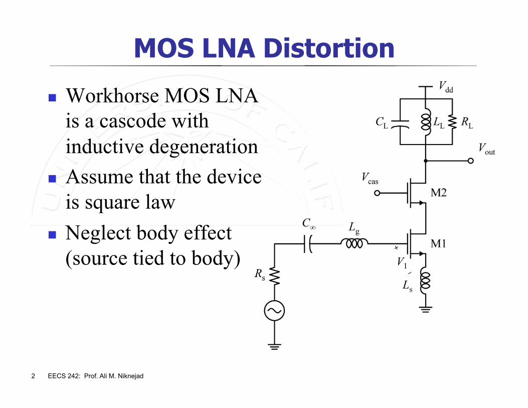
MOS LNA Distortion
Workhorse MOS LNA is a cascode with inductive degeneration
Assume that the device is square law
Neglect body effect (source tied to body)
3 EECS 242: Prof. Ali M. Niknejad
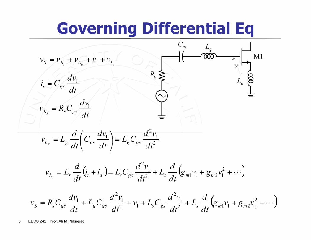
Governing Differential Eq
4 EECS 242: Prof. Ali M. Niknejad
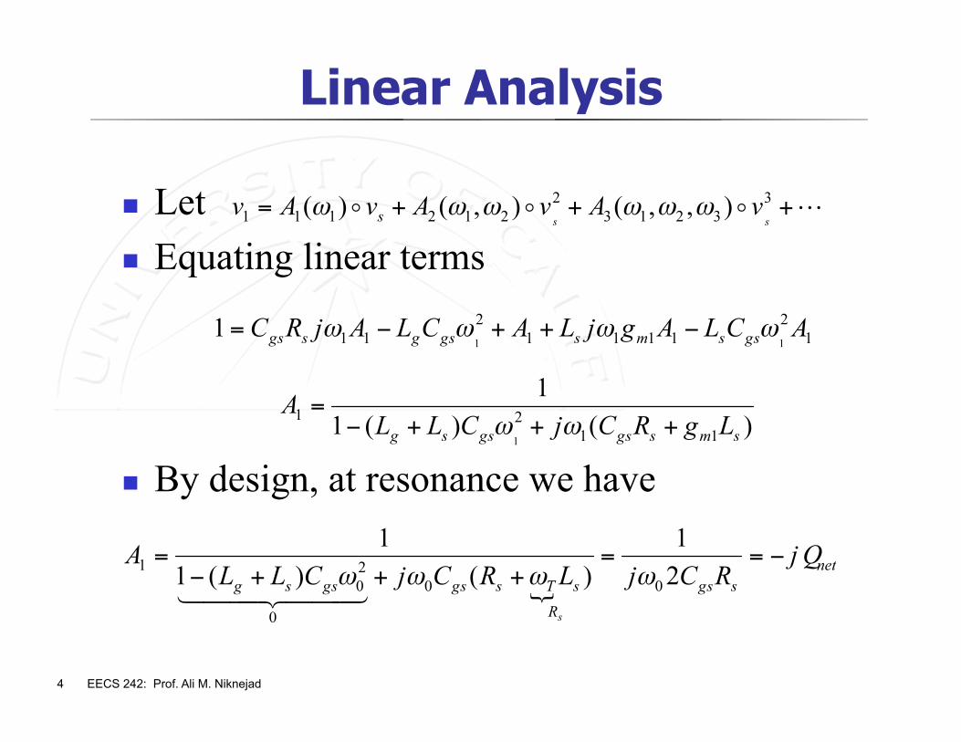
Linear Analysis
Let Equating linear terms
By design, at resonance we have
5 EECS 242: Prof. Ali M. Niknejad
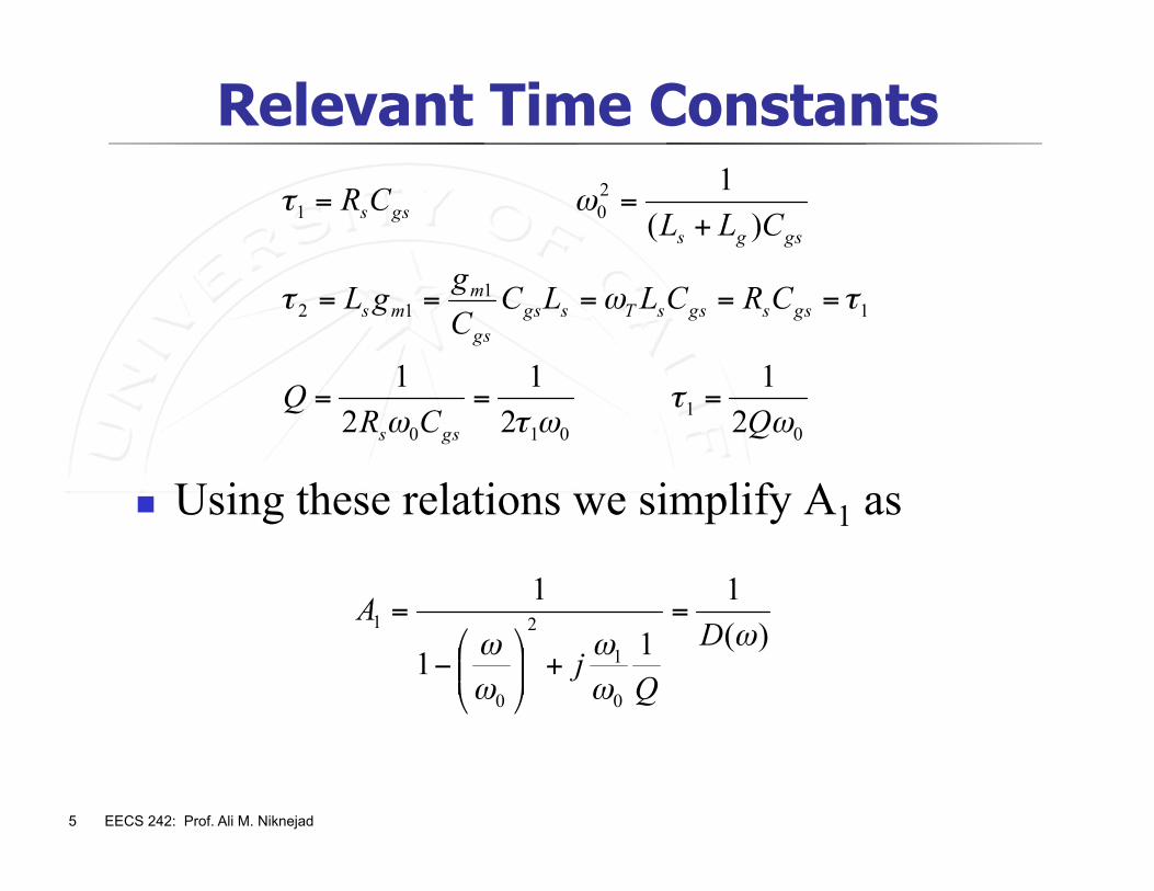
Relevant Time Constants
Using these relations we simplify A1 as
6 EECS 242: Prof. Ali M. Niknejad
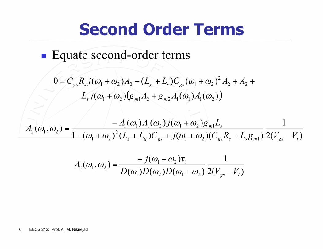
Second Order Terms Equate second-order terms
7 EECS 242: Prof. Ali M. Niknejad
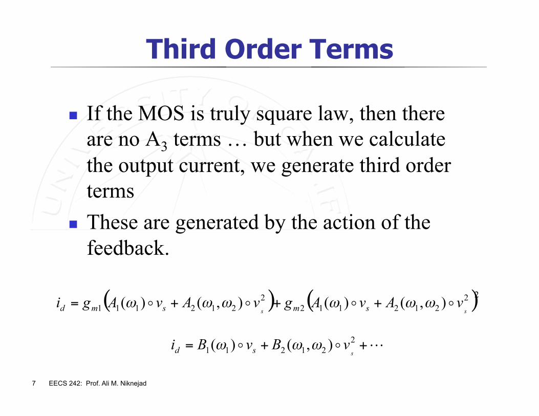
Third Order Terms
If the MOS is truly square law, then there are no A3 terms … but when we calculate the output current, we generate third order terms
These are generated by the action of the feedback.
8 EECS 242: Prof. Ali M. Niknejad
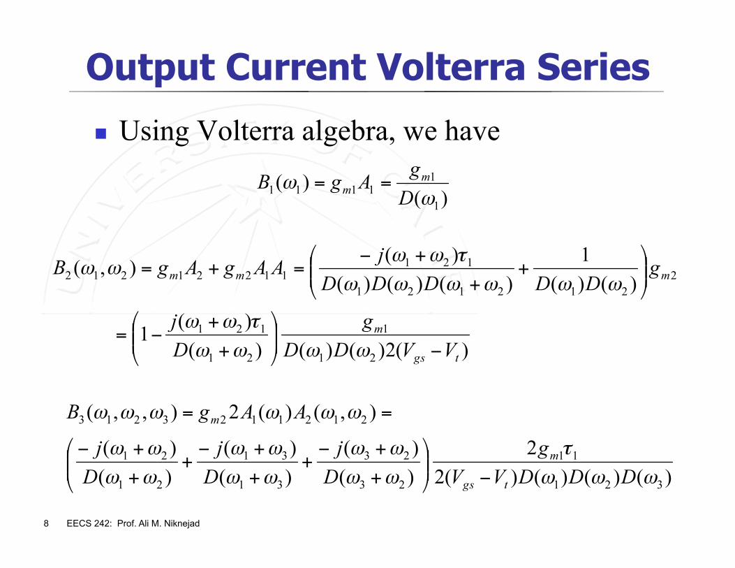
Output Current Volterra Series
Using Volterra algebra, we have
9 EECS 242: Prof. Ali M. Niknejad
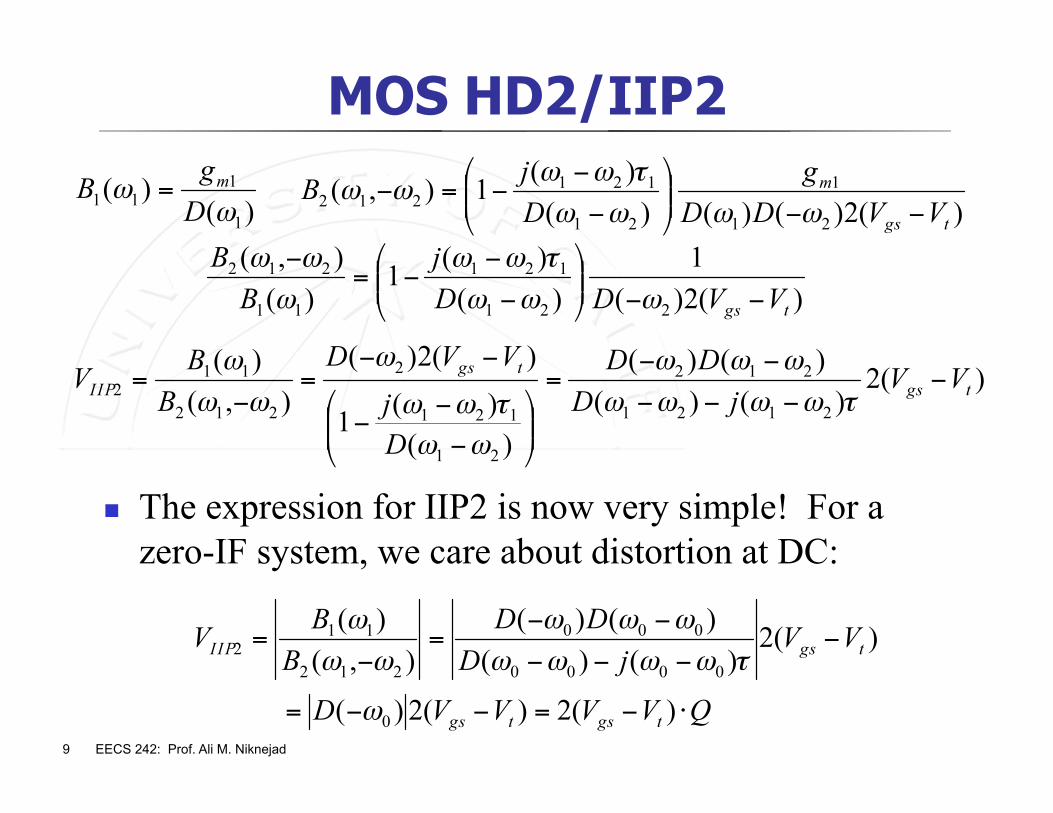
MOS HD2/IIP2
The expression for IIP2 is now very simple! For a zero-IF system, we care about distortion at DC:
10 EECS 242: Prof. Ali M. Niknejad
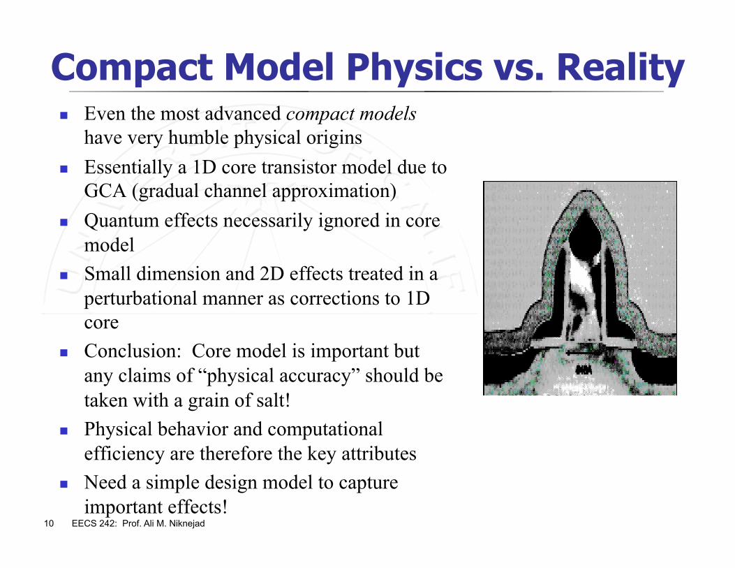
Compact Model Physics vs. Reality Even the most advanced compact models
have very humble physical origins Essentially a 1D core transistor model due to
GCA (gradual channel approximation) Quantum effects necessarily ignored in core
model Small dimension and 2D effects treated in a
perturbational manner as corrections to 1D core
Conclusion: Core model is important but any claims of “physical accuracy” should be taken with a grain of salt!
Physical behavior and computational efficiency are therefore the key attributes
Need a simple design model to capture important effects!
11 EECS 242: Prof. Ali M. Niknejad
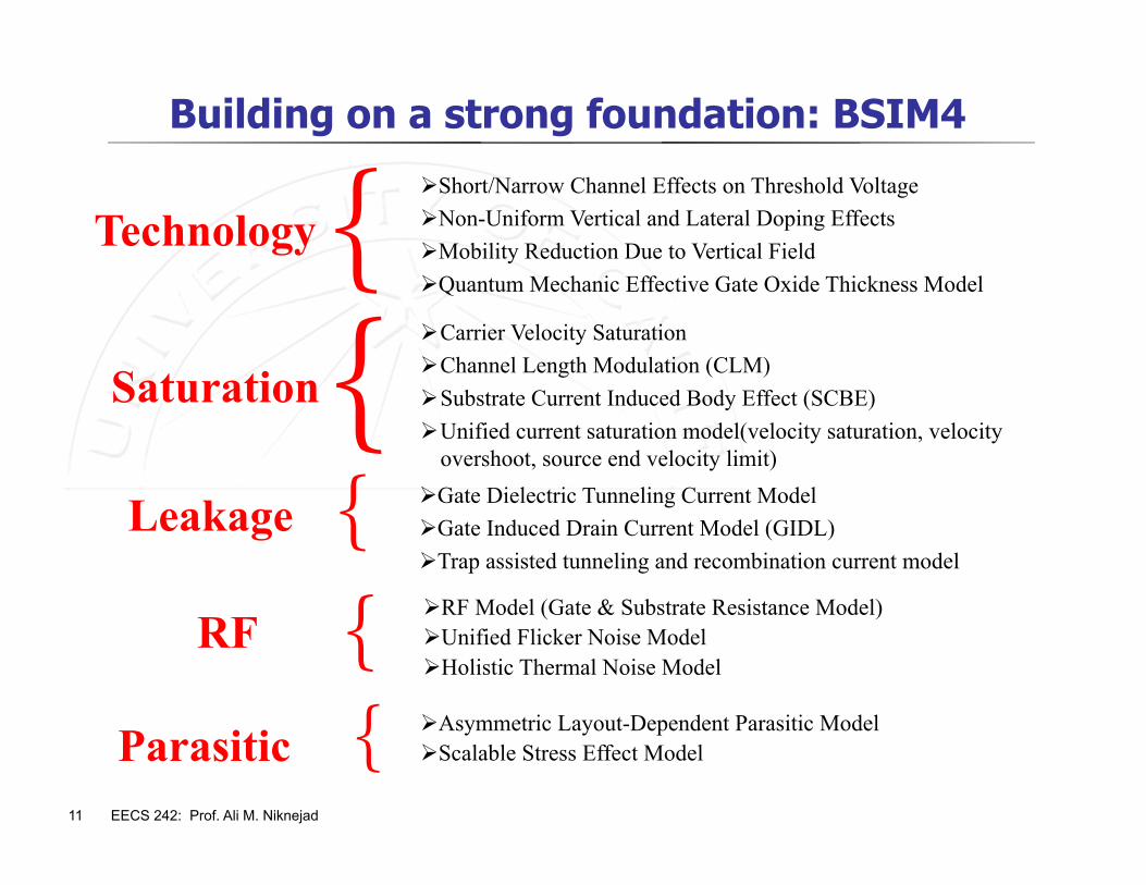
Parasitic { Asymmetric Layout-Dependent Parasitic Model Scalable Stress Effect Model
RF { RF Model (Gate & Substrate Resistance Model) Unified Flicker Noise Model Holistic Thermal Noise Model
Leakage { Gate Dielectric Tunneling Current Model Gate Induced Drain Current Model (GIDL) Trap assisted tunneling and recombination current model
Carrier Velocity Saturation Channel Length Modulation (CLM) Substrate Current Induced Body Effect (SCBE) Unified current saturation model(velocity saturation, velocity
overshoot, source end velocity limit)
Saturation {
Short/Narrow Channel Effects on Threshold Voltage Non-Uniform Vertical and Lateral Doping Effects Mobility Reduction Due to Vertical Field Quantum Mechanic Effective Gate Oxide Thickness Model
Technology {Building on a strong foundation: BSIM4
12 EECS 242: Prof. Ali M. Niknejad
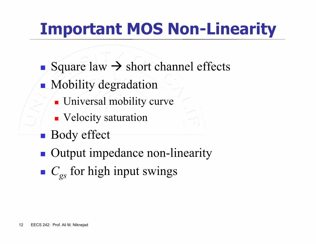
Important MOS Non-Linearity
Square law short channel effects Mobility degradation
Universal mobility curve Velocity saturation
Body effect Output impedance non-linearity Cgs for high input swings
13 EECS 242: Prof. Ali M. Niknejad
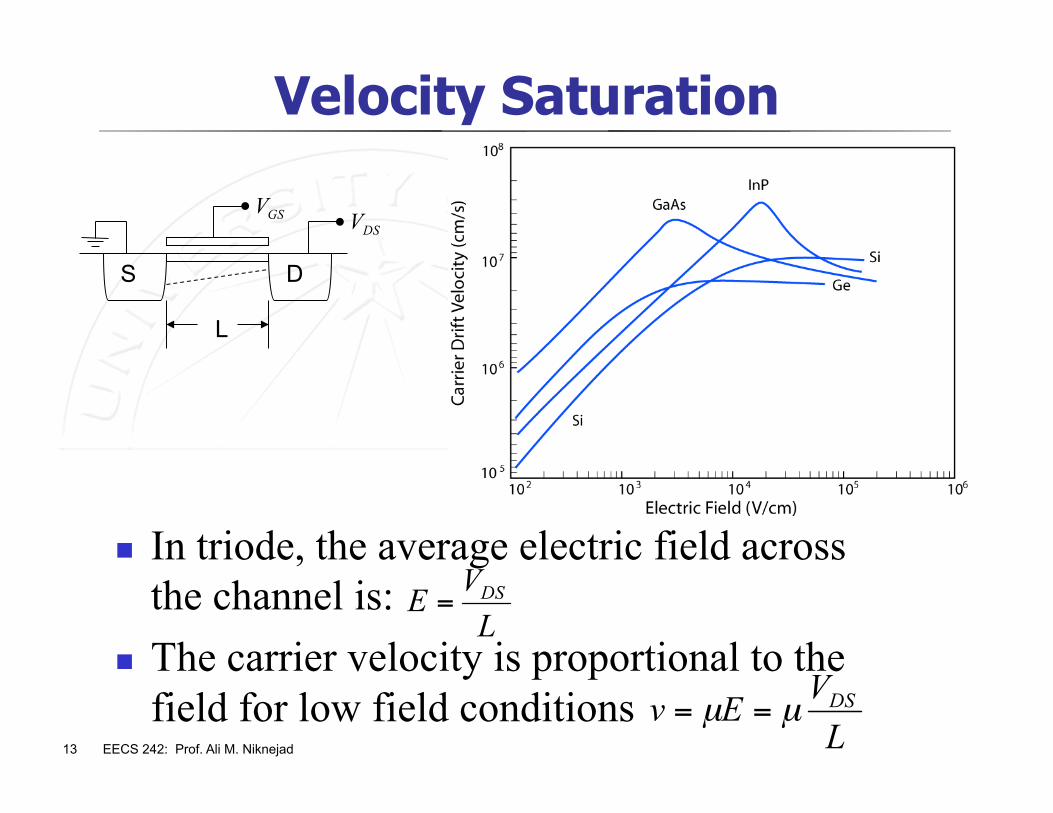
Velocity Saturation
In triode, the average electric field across the channel is:
The carrier velocity is proportional to the field for low field conditions
S D
L
14 EECS 242: Prof. Ali M. Niknejad
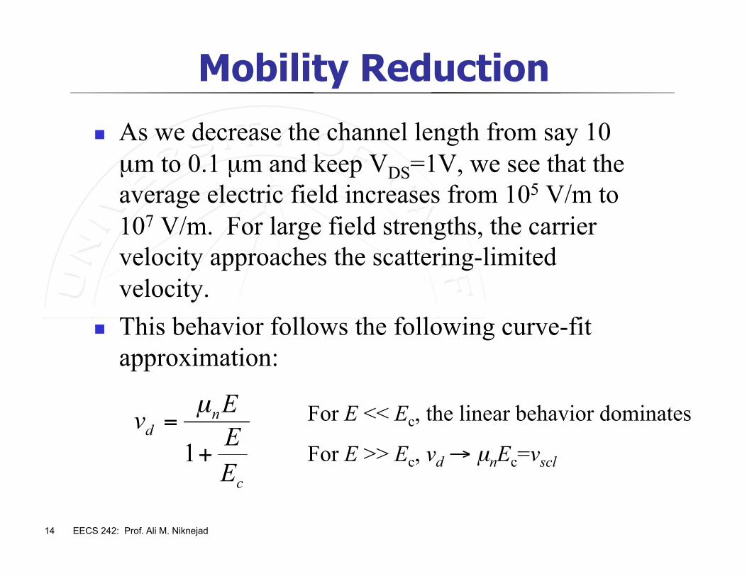
Mobility Reduction As we decrease the channel length from say 10 µm to 0.1 µm and keep VDS=1V, we see that the average electric field increases from 105 V/m to 107 V/m. For large field strengths, the carrier velocity approaches the scattering-limited velocity.
This behavior follows the following curve-fit approximation:
For E << Ec, the linear behavior dominates
For E >> Ec, vd → µnEc=vscl
15 EECS 242: Prof. Ali M. Niknejad
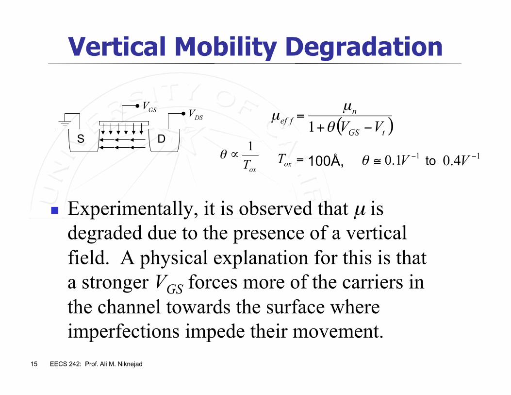
Vertical Mobility Degradation
Experimentally, it is observed that µ is degraded due to the presence of a vertical field. A physical explanation for this is that a stronger VGS forces more of the carriers in the channel towards the surface where imperfections impede their movement.
S D
100Å, to
16 EECS 242: Prof. Ali M. Niknejad
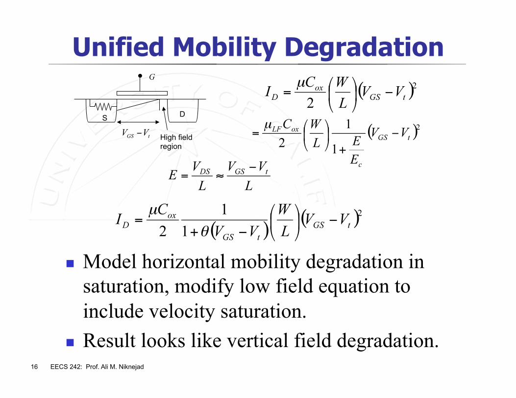
Unified Mobility Degradation
Model horizontal mobility degradation in saturation, modify low field equation to include velocity saturation.
Result looks like vertical field degradation.
S D
High field region
17 EECS 242: Prof. Ali M. Niknejad
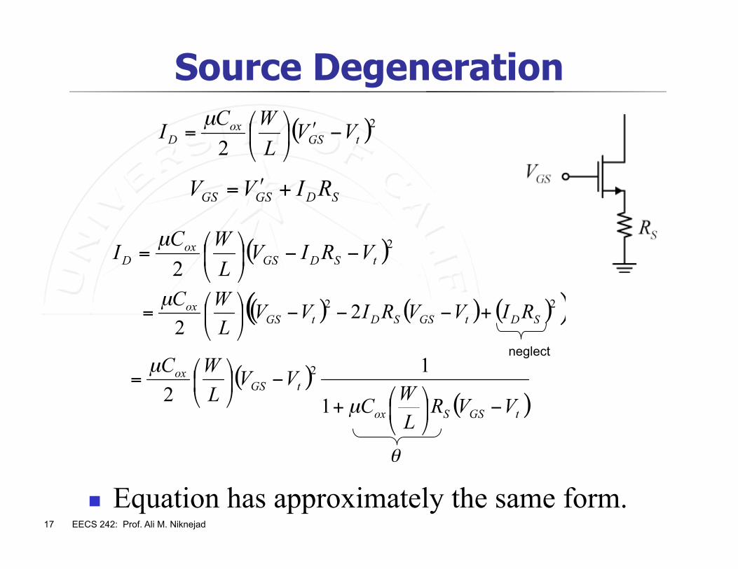
Source Degeneration
Equation has approximately the same form.
neglect
18 EECS 242: Prof. Ali M. Niknejad
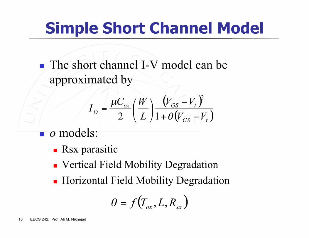
Simple Short Channel Model
The short channel I-V model can be approximated by
ɵ models: Rsx parasitic Vertical Field Mobility Degradation Horizontal Field Mobility Degradation
19 EECS 242: Prof. Ali M. Niknejad
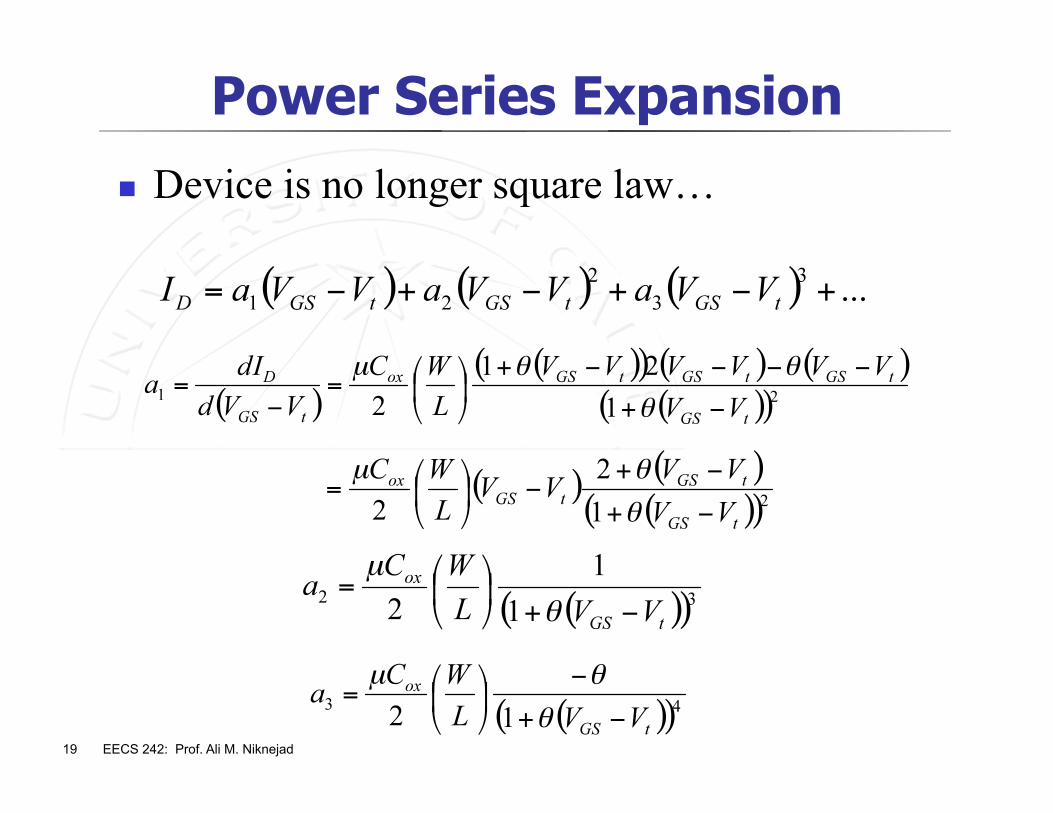
Power Series Expansion Device is no longer square law…
20 EECS 242: Prof. Ali M. Niknejad
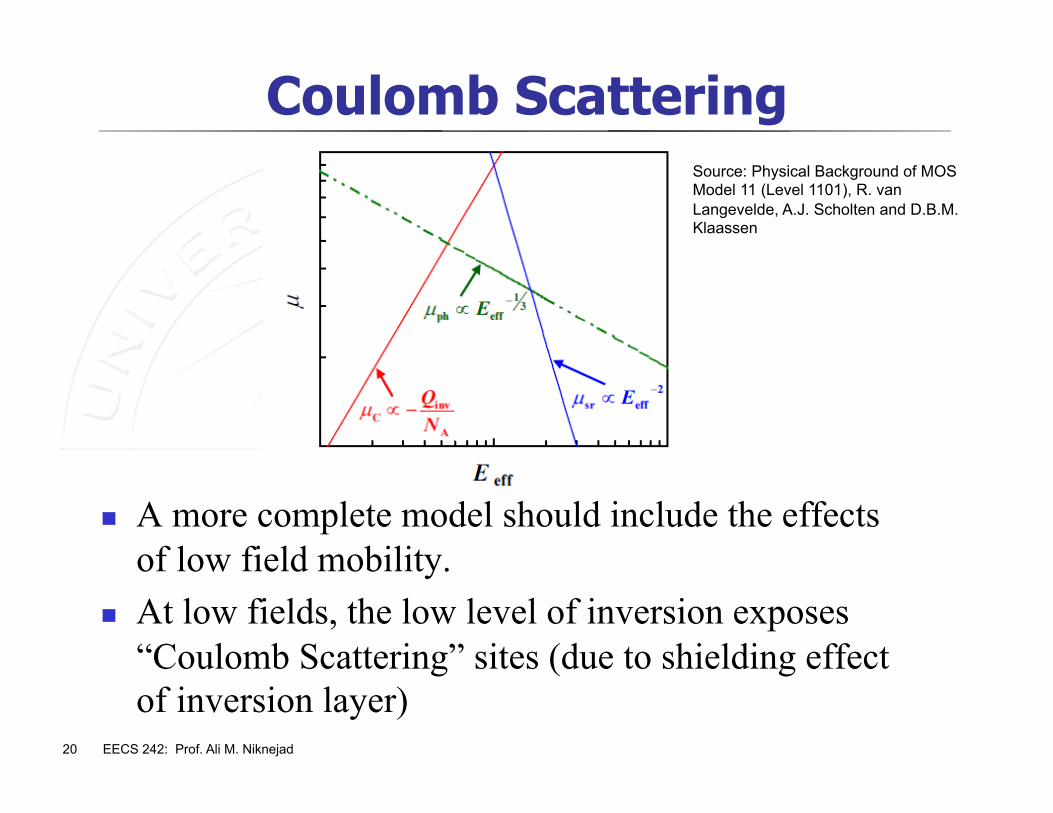
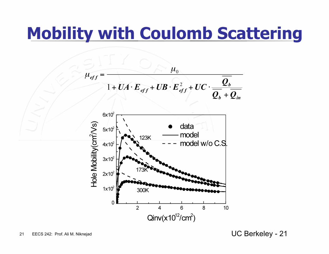
Coulomb Scattering
A more complete model should include the effects of low field mobility.
At low fields, the low level of inversion exposes “Coulomb Scattering” sites (due to shielding effect of inversion layer)
Source: Physical Background of MOS Model 11 (Level 1101), R. van Langevelde, A.J. Scholten and D.B.M. Klaassen
21 EECS 242: Prof. Ali M. Niknejad
Mobility with Coulomb Scattering
UC Berkeley - 21
22 EECS 242: Prof. Ali M. Niknejad
Need for Single Equation I-V
Our models up to now only include strong inversion. In many applications, we would like a model to capture the entire I-V range from weak inversion to moderate inversion to strong inversion Hard switching transistor Power amplifiers, mixers, VCOs
Surface potential models do this in a natural way but are implicit equations and more appropriate for numerical techniques
23 EECS 242: Prof. Ali M. Niknejad
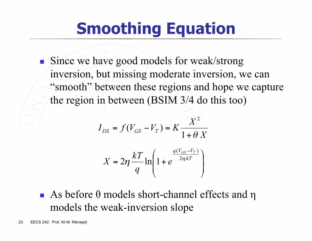
Smoothing Equation
Since we have good models for weak/strong inversion, but missing moderate inversion, we can “smooth” between these regions and hope we capture the region in between (BSIM 3/4 do this too)
As before θ models short-channel effects and η models the weak-inversion slope
24 EECS 242: Prof. Ali M. Niknejad
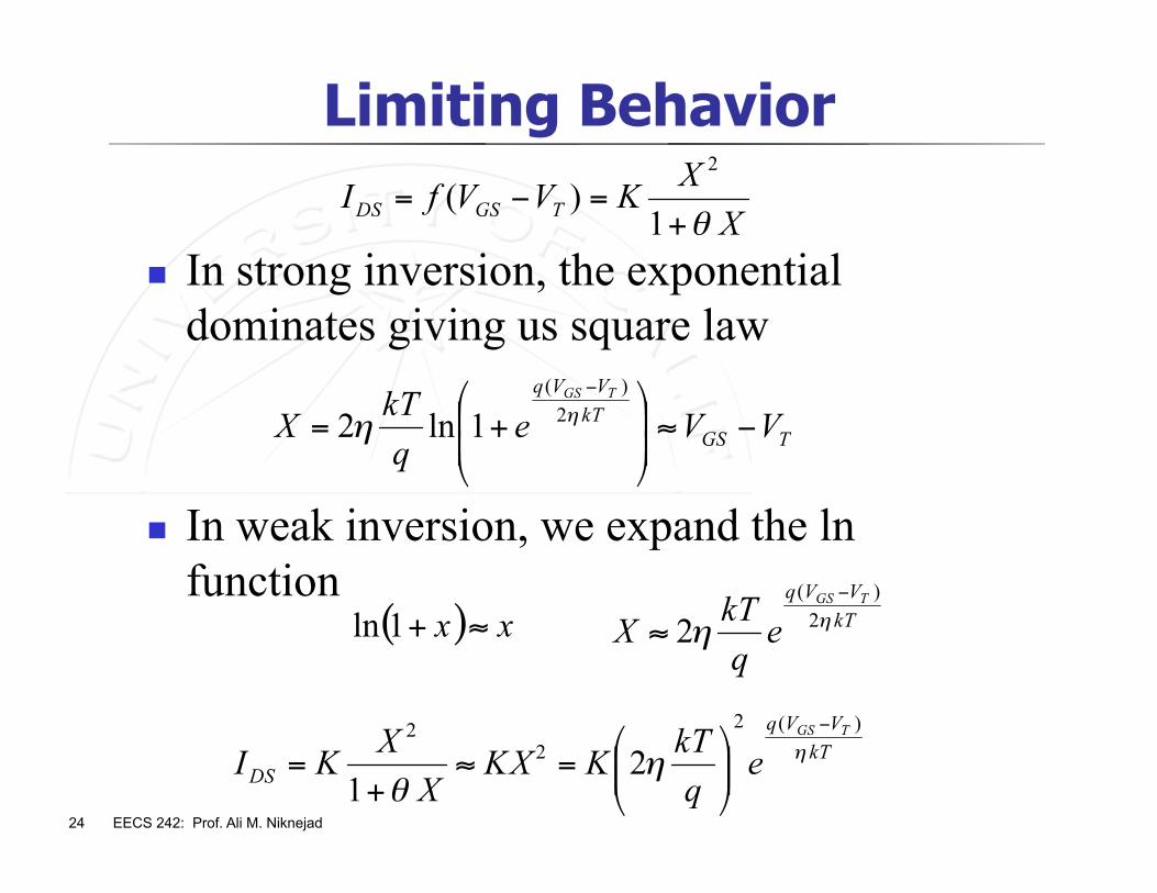
Limiting Behavior
In strong inversion, the exponential dominates giving us square law
In weak inversion, we expand the ln function
25 EECS 242: Prof. Ali M. Niknejad
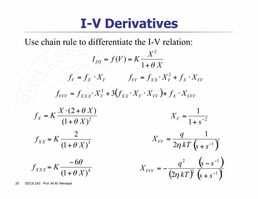
I-V Derivatives Use chain rule to differentiate the I-V relation:
26 EECS 242: Prof. Ali M. Niknejad
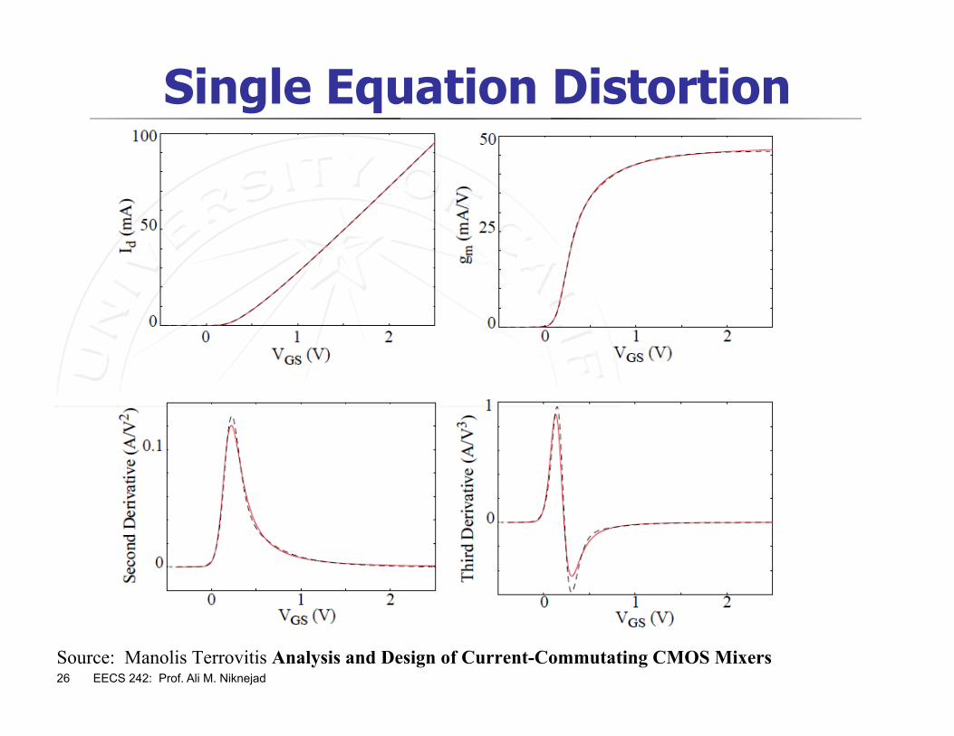
Single Equation Distortion
Source: Manolis Terrovitis Analysis and Design of Current-Commutating CMOS Mixers
27 EECS 242: Prof. Ali M. Niknejad
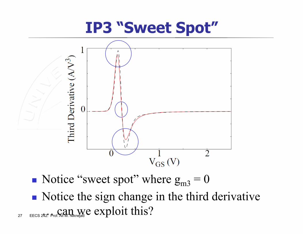
IP3 “Sweet Spot”
Notice “sweet spot” where gm3 = 0 Notice the sign change in the third derivative
… can we exploit this?
28 EECS 242: Prof. Ali M. Niknejad
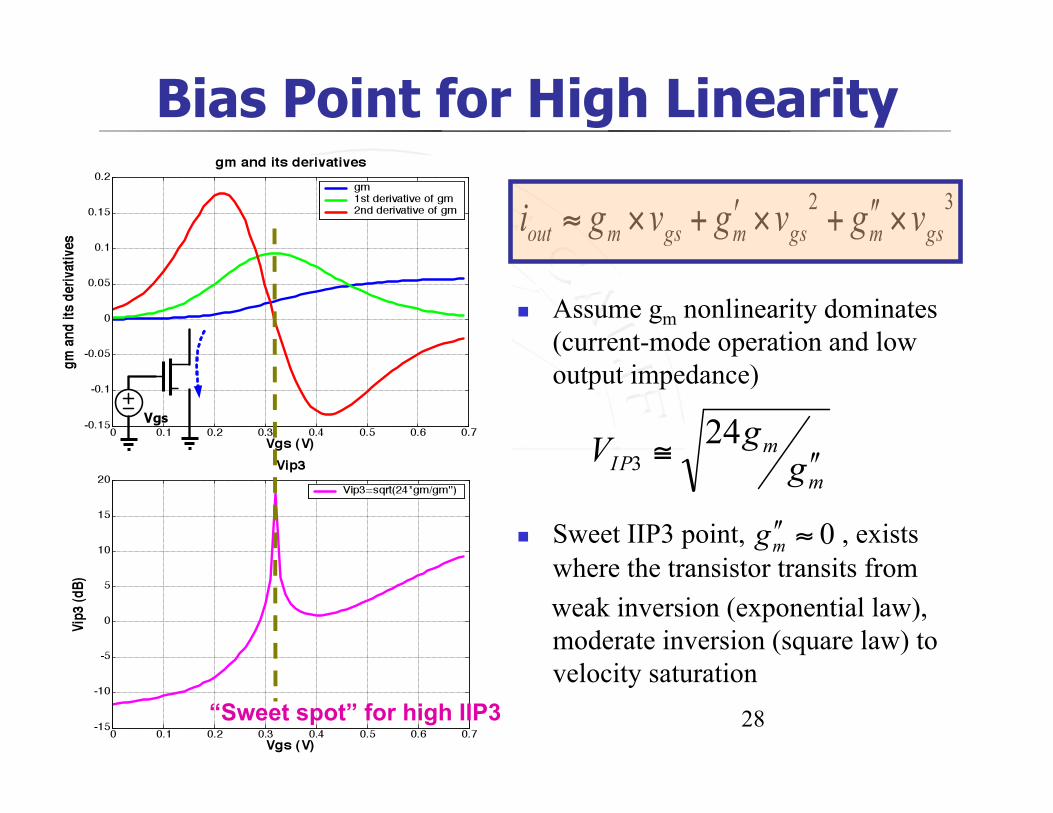
Bias Point for High Linearity
Assume gm nonlinearity dominates (current-mode operation and low output impedance)
Sweet IIP3 point, , exists where the transistor transits from
weak inversion (exponential law), moderate inversion (square law) to velocity saturation
“Sweet spot” for high IIP3 28
29 EECS 242: Prof. Ali M. Niknejad
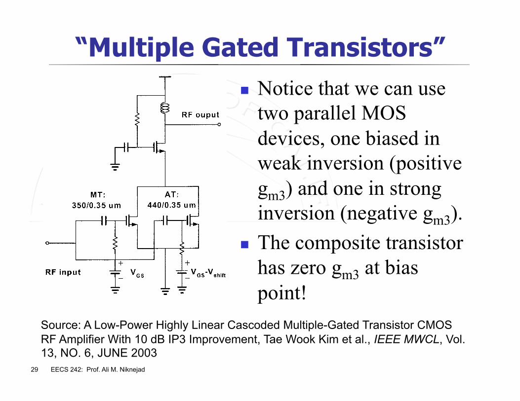
“Multiple Gated Transistors” Notice that we can use
two parallel MOS devices, one biased in weak inversion (positive gm3) and one in strong inversion (negative gm3).
The composite transistor has zero gm3 at bias point!
Source: A Low-Power Highly Linear Cascoded Multiple-Gated Transistor CMOS RF Amplifier With 10 dB IP3 Improvement, Tae Wook Kim et al., IEEE MWCL, Vol. 13, NO. 6, JUNE 2003
30 EECS 242: Prof. Ali M. Niknejad
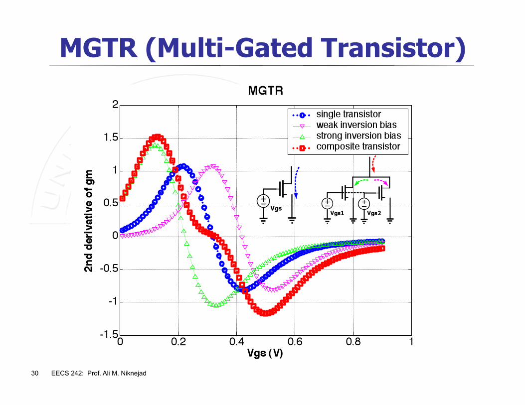
MGTR (Multi-Gated Transistor)
31 EECS 242: Prof. Ali M. Niknejad
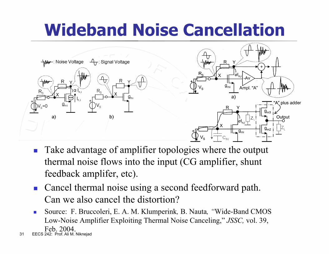
Wideband Noise Cancellation
Take advantage of amplifier topologies where the output thermal noise flows into the input (CG amplifier, shunt feedback amplifer, etc).
Cancel thermal noise using a second feedforward path. Can we also cancel the distortion?
Source: F. Bruccoleri, E. A. M. Klumperink, B. Nauta, “Wide-Band CMOS Low-Noise Amplifier Exploiting Thermal Noise Canceling,” JSSC, vol. 39, Feb. 2004.
32 EECS 242: Prof. Ali M. Niknejad
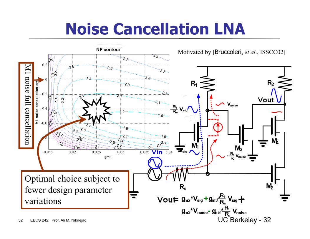
Noise Cancellation LNA Motivated by [Bruccoleri, et al., ISSCC02]
M1 noise full cancellation
Optimal choice subject to fewer design parameter variations
UC Berkeley - 32
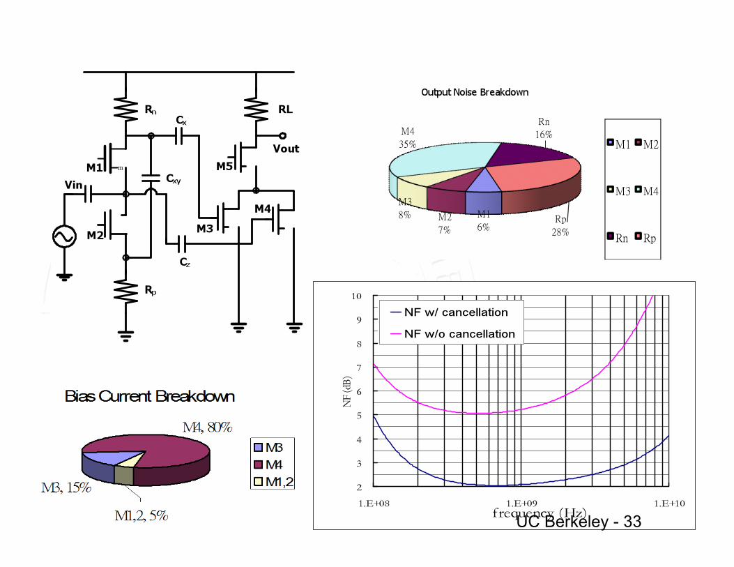
33 EECS 242: Prof. Ali M. Niknejad UC Berkeley - 33
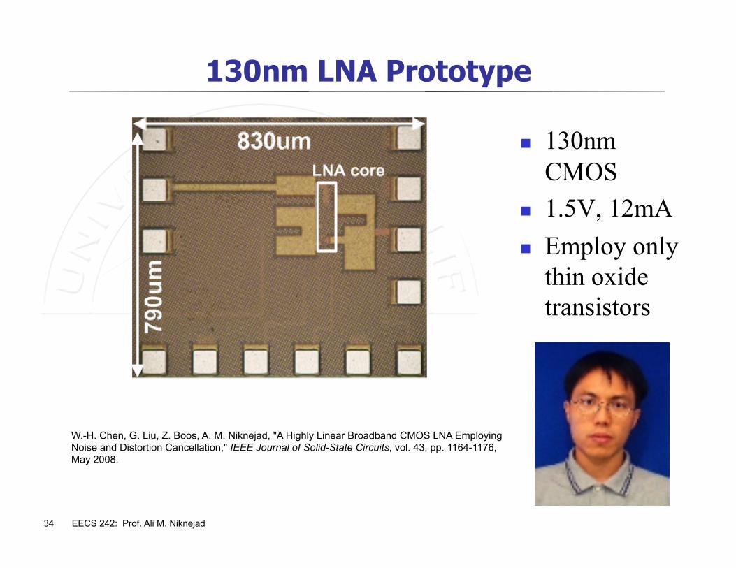
34 EECS 242: Prof. Ali M. Niknejad
130nm LNA Prototype
130nm CMOS
1.5V, 12mA Employ only
thin oxide transistors
W.-H. Chen, G. Liu, Z. Boos, A. M. Niknejad, "A Highly Linear Broadband CMOS LNA Employing Noise and Distortion Cancellation," IEEE Journal of Solid-State Circuits, vol. 43, pp. 1164-1176, May 2008.
35 EECS 242: Prof. Ali M. Niknejad
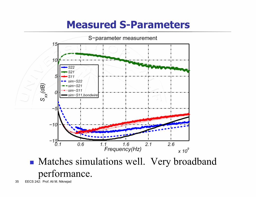
Measured S-Parameters
Matches simulations well. Very broadband performance.
36 EECS 242: Prof. Ali M. Niknejad
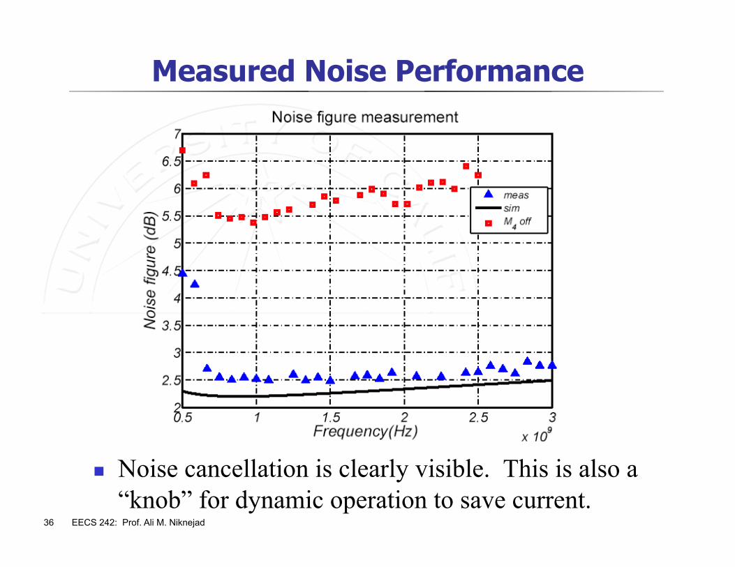
Measured Noise Performance
Noise cancellation is clearly visible. This is also a “knob” for dynamic operation to save current.
37 EECS 242: Prof. Ali M. Niknejad
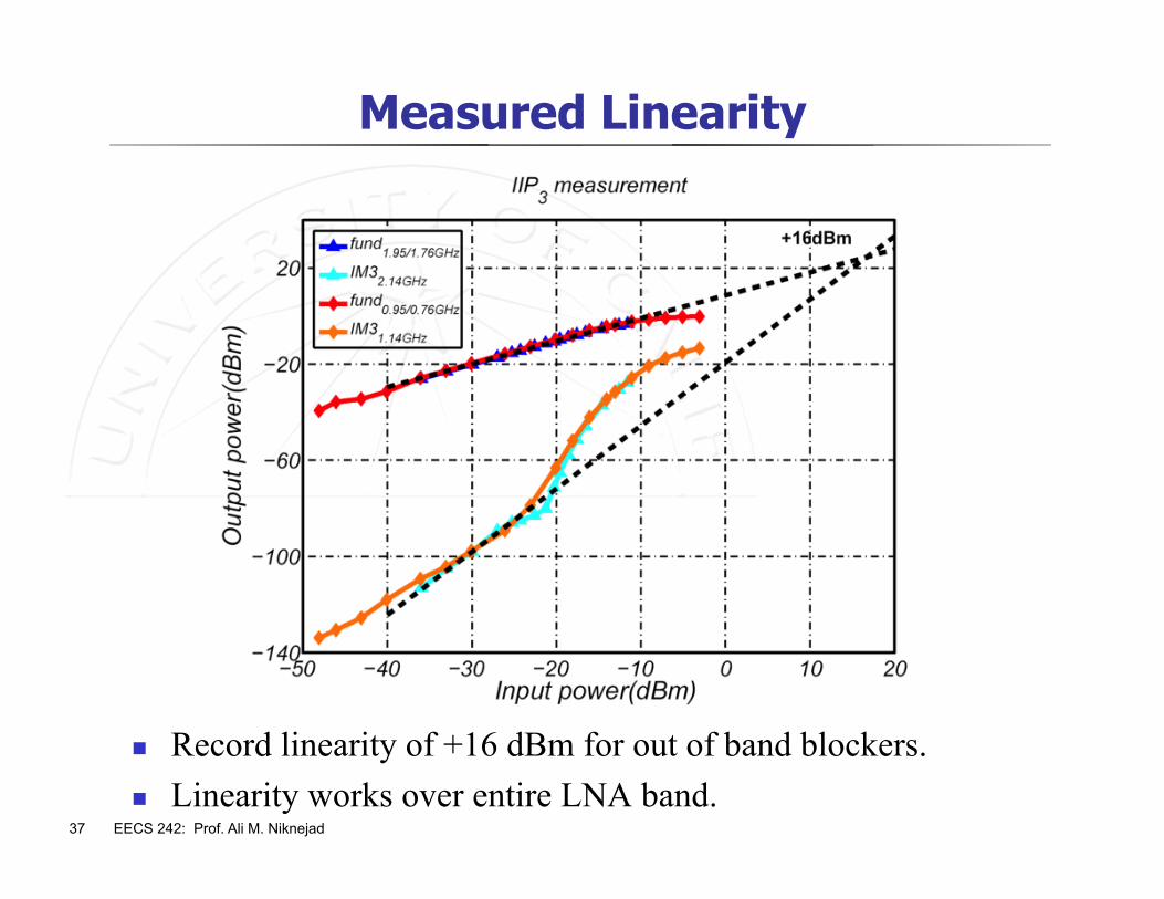
Measured Linearity
Record linearity of +16 dBm for out of band blockers. Linearity works over entire LNA band.
38 EECS 242: Prof. Ali M. Niknejad
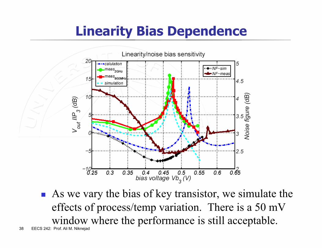
Linearity Bias Dependence
As we vary the bias of key transistor, we simulate the effects of process/temp variation. There is a 50 mV window where the performance is still acceptable.
39 EECS 242: Prof. Ali M. Niknejad
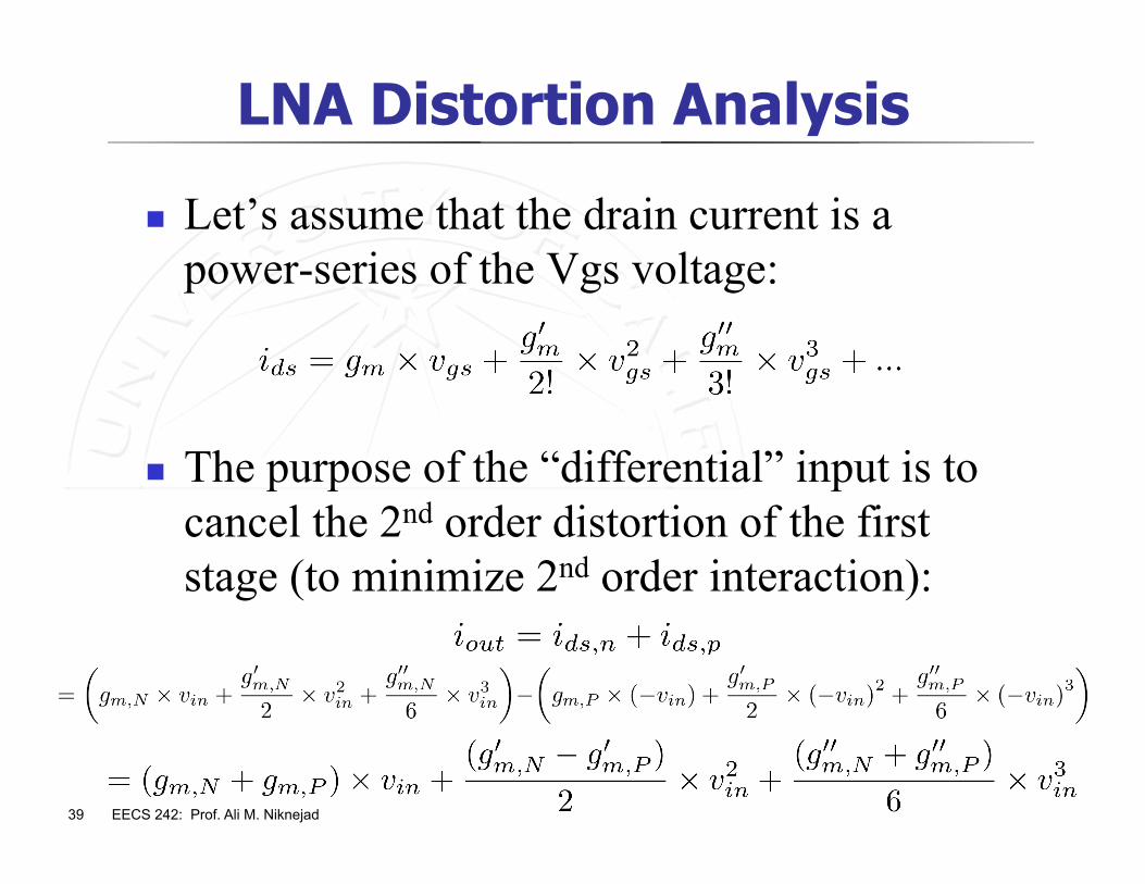
LNA Distortion Analysis
Let’s assume that the drain current is a power-series of the Vgs voltage:
The purpose of the “differential” input is to cancel the 2nd order distortion of the first stage (to minimize 2nd order interaction):
40 EECS 242: Prof. Ali M. Niknejad
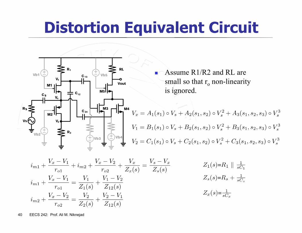
Distortion Equivalent Circuit
Assume R1/R2 and RL are small so that ro non-linearity is ignored.
41 EECS 242: Prof. Ali M. Niknejad
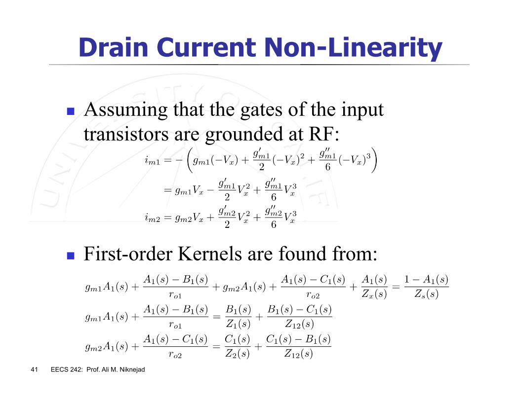
Drain Current Non-Linearity
Assuming that the gates of the input transistors are grounded at RF:
First-order Kernels are found from:
42 EECS 242: Prof. Ali M. Niknejad
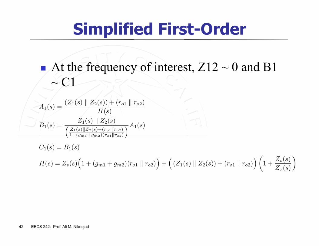
Simplified First-Order
At the frequency of interest, Z12 ~ 0 and B1 ~ C1
43 EECS 242: Prof. Ali M. Niknejad
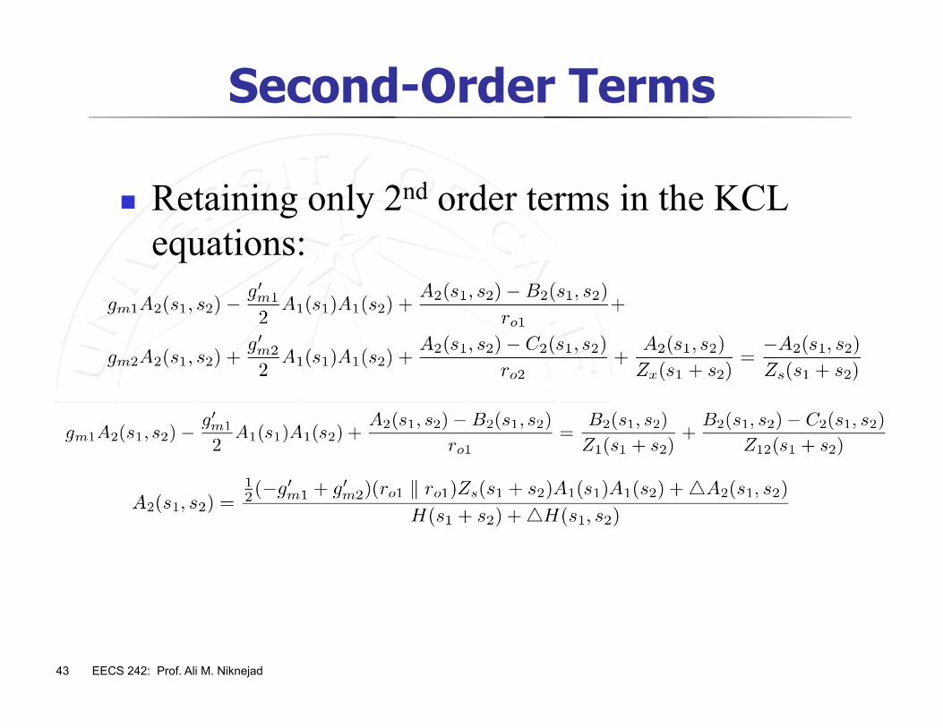
Second-Order Terms
Retaining only 2nd order terms in the KCL equations:
44 EECS 242: Prof. Ali M. Niknejad
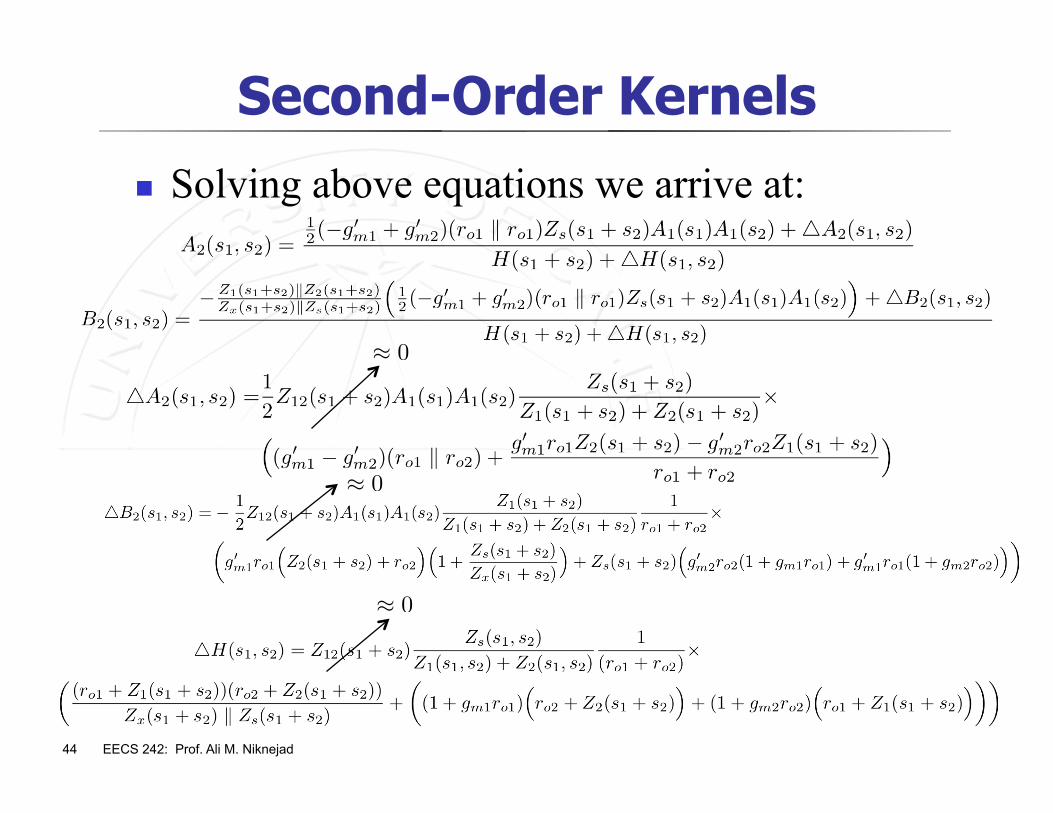
Second-Order Kernels Solving above equations we arrive at:
! 0
! 0
! 0
45 EECS 242: Prof. Ali M. Niknejad
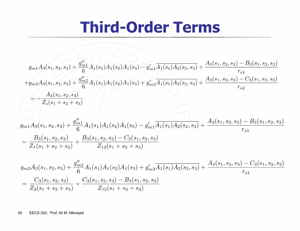
Third-Order Terms
46 EECS 242: Prof. Ali M. Niknejad
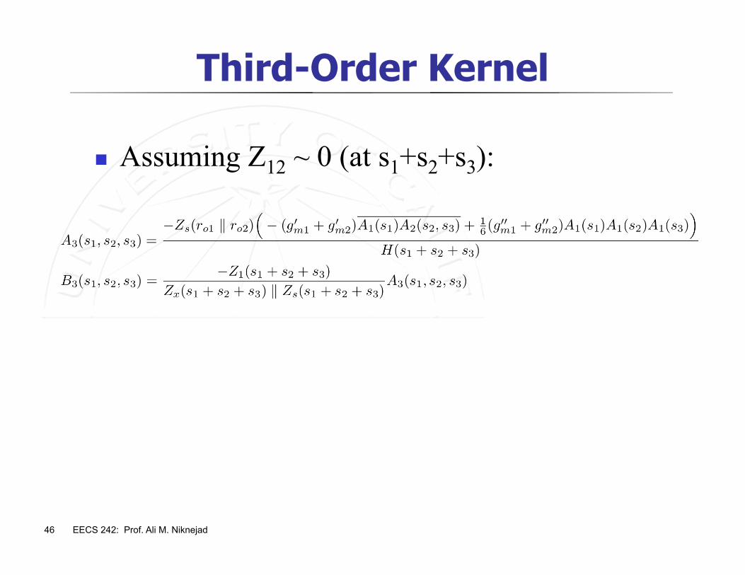
Third-Order Kernel
Assuming Z12 ~ 0 (at s1+s2+s3):
47 EECS 242: Prof. Ali M. Niknejad
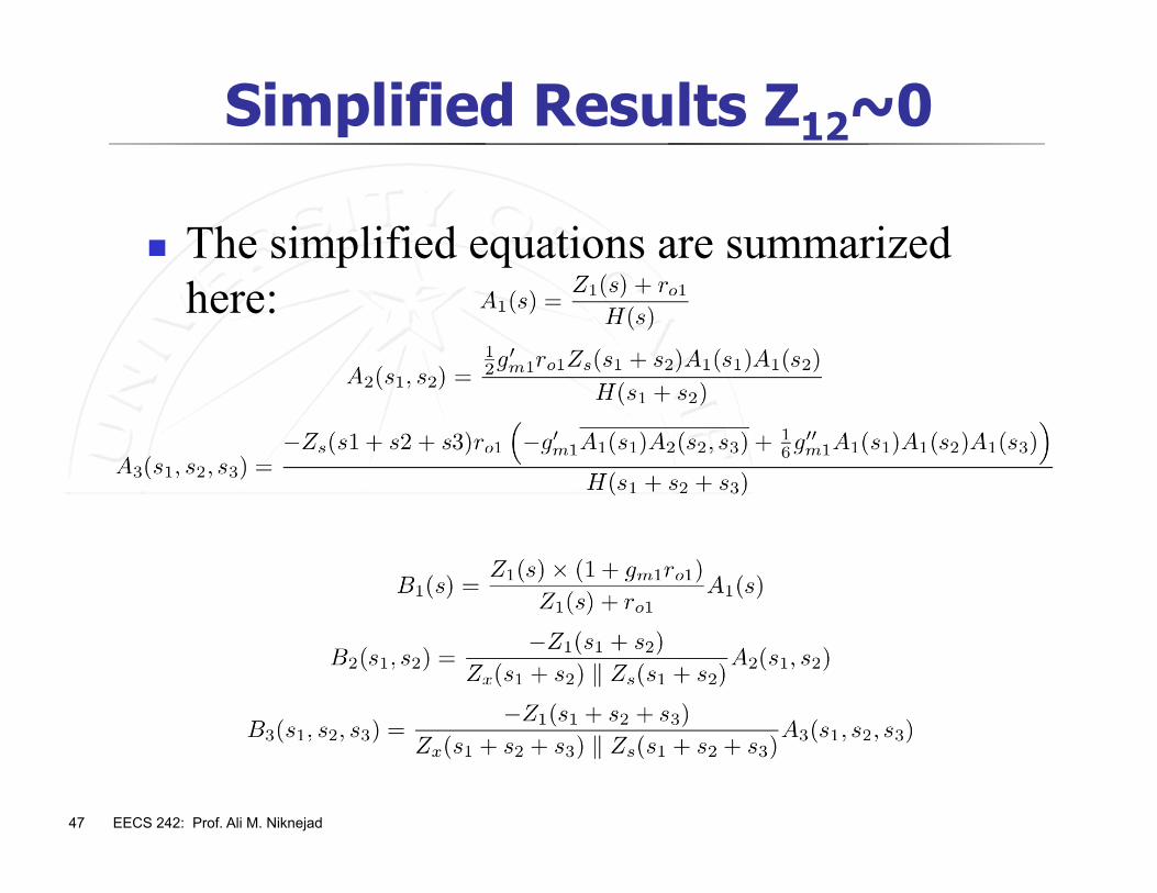
Simplified Results Z12~0
The simplified equations are summarized here:
48 EECS 242: Prof. Ali M. Niknejad
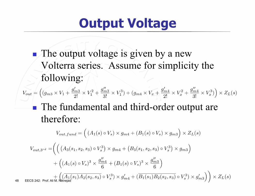
Output Voltage
The output voltage is given by a new Volterra series. Assume for simplicity the following:
The fundamental and third-order output are therefore:
49 EECS 242: Prof. Ali M. Niknejad
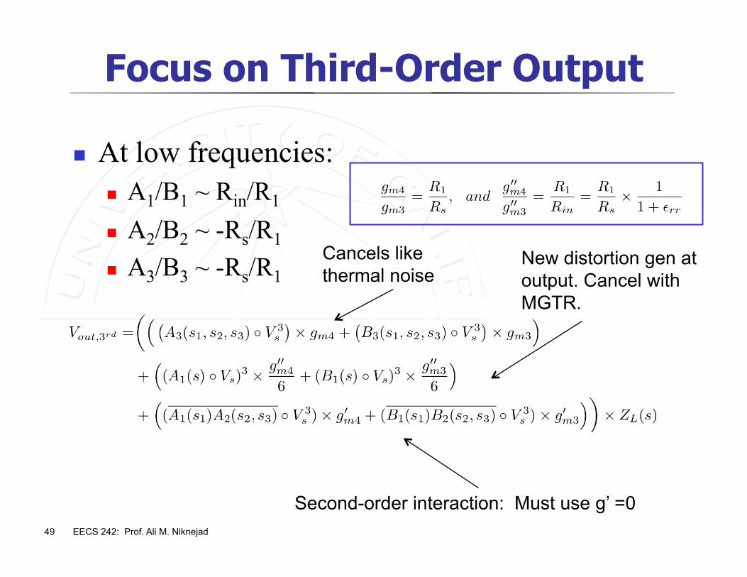
Focus on Third-Order Output
At low frequencies: A1/B1 ~ Rin/R1
A2/B2 ~ -Rs/R1
A3/B3 ~ -Rs/R1 Cancels like thermal noise
Second-order interaction: Must use g’ =0
New distortion gen at output. Cancel with MGTR.
50 EECS 242: Prof. Ali M. Niknejad
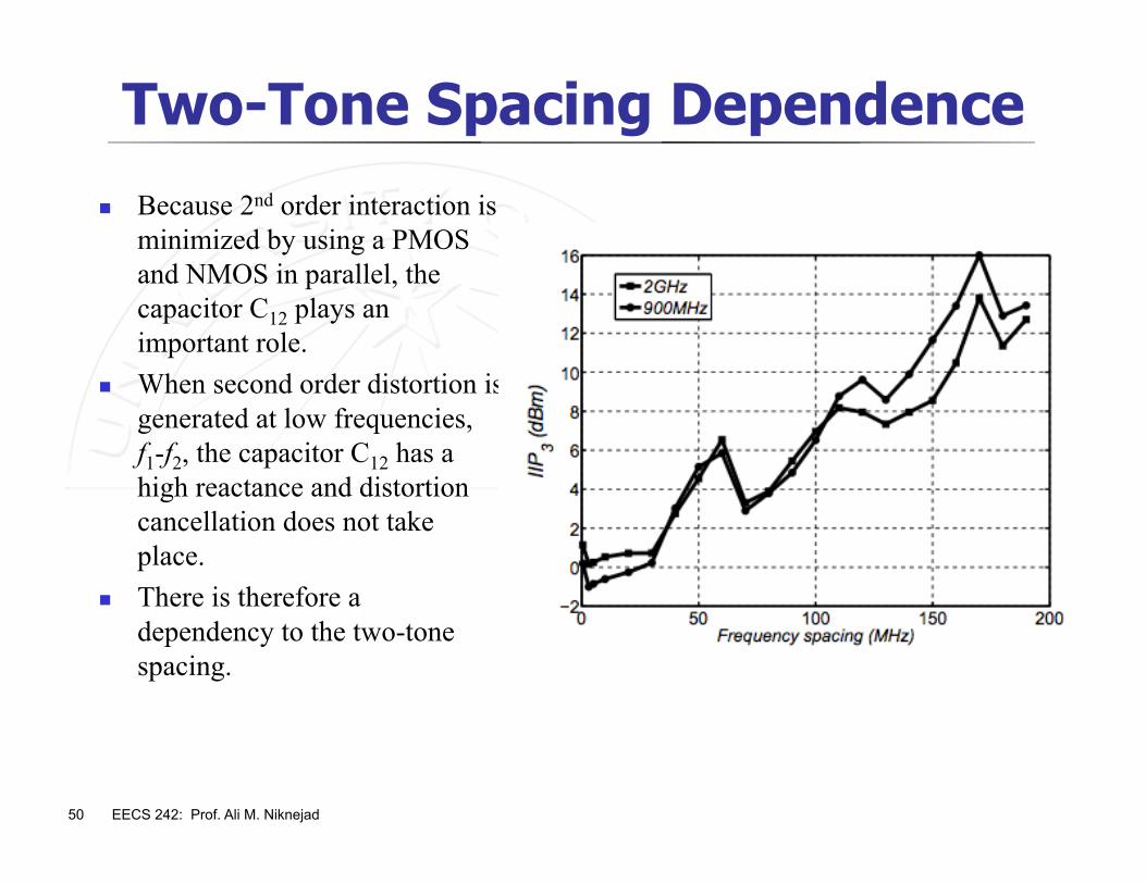
Two-Tone Spacing Dependence Because 2nd order interaction is
minimized by using a PMOS and NMOS in parallel, the capacitor C12 plays an important role.
When second order distortion is generated at low frequencies, f1-f2, the capacitor C12 has a high reactance and distortion cancellation does not take place.
There is therefore a dependency to the two-tone spacing.
51 EECS 242: Prof. Ali M. Niknejad
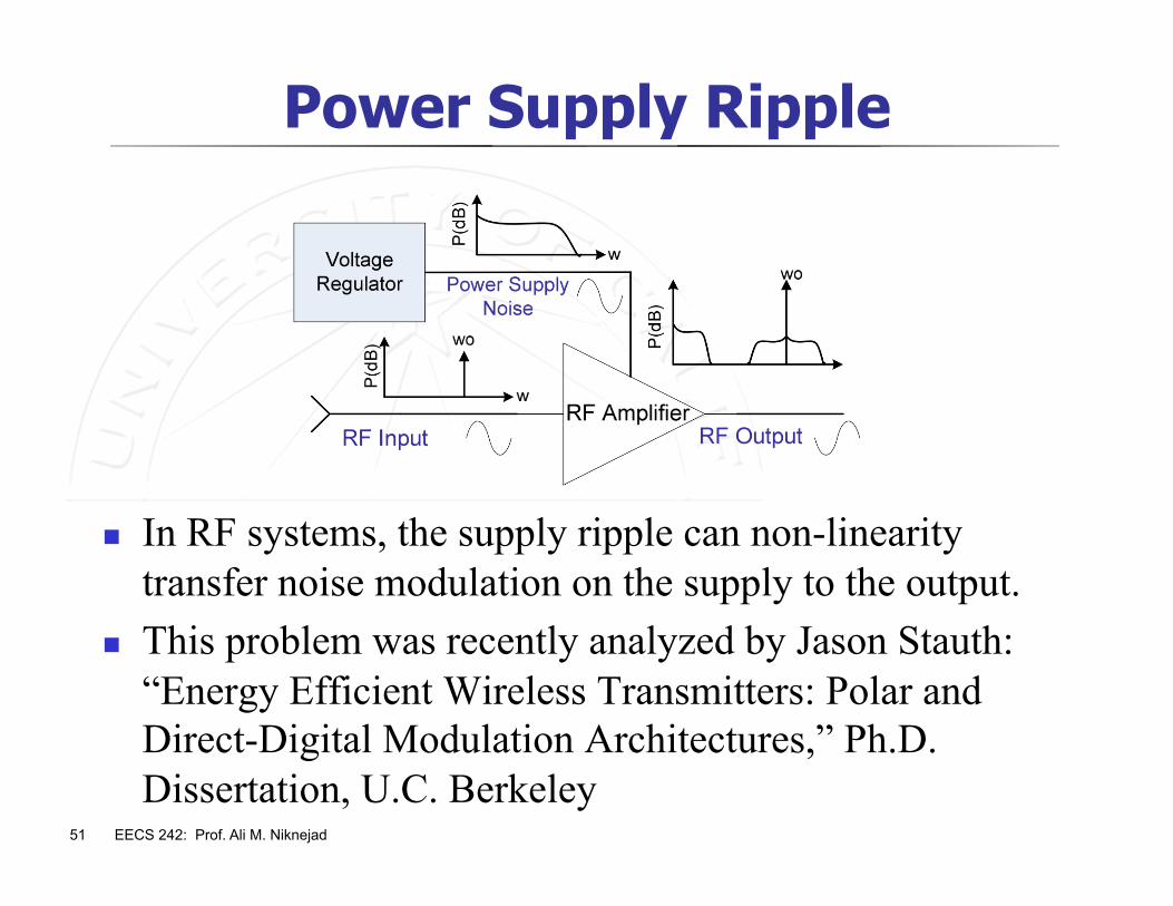
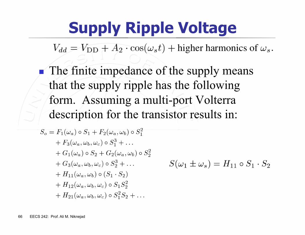
Power Supply Ripple
In RF systems, the supply ripple can non-linearity transfer noise modulation on the supply to the output.
This problem was recently analyzed by Jason Stauth: “Energy Efficient Wireless Transmitters: Polar and Direct-Digital Modulation Architectures,” Ph.D. Dissertation, U.C. Berkeley
52 EECS 242: Prof. Ali M. Niknejad
Supply Noise Sources
53 EECS 242: Prof. Ali M. Niknejad
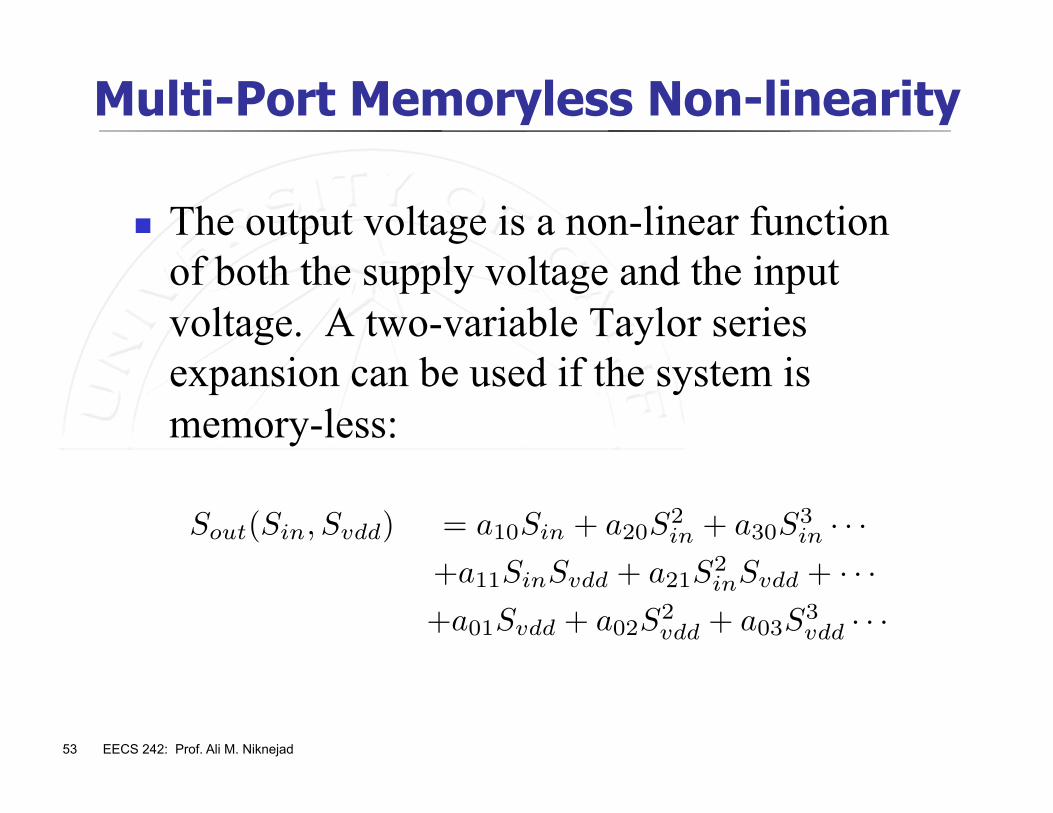
Multi-Port Memoryless Non-linearity
The output voltage is a non-linear function of both the supply voltage and the input voltage. A two-variable Taylor series expansion can be used if the system is memory-less:
Sout(Sin, Svdd) = a10Sin + a20S2in + a30S3
in · · ·+a11SinSvdd + a21S2
inSvdd + · · ·+a01Svdd + a02S2
vdd + a03S3vdd · · ·
54 EECS 242: Prof. Ali M. Niknejad
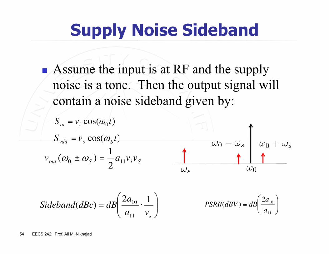
Supply Noise Sideband
Assume the input is at RF and the supply noise is a tone. Then the output signal will contain a noise sideband given by:
55 EECS 242: Prof. Ali M. Niknejad
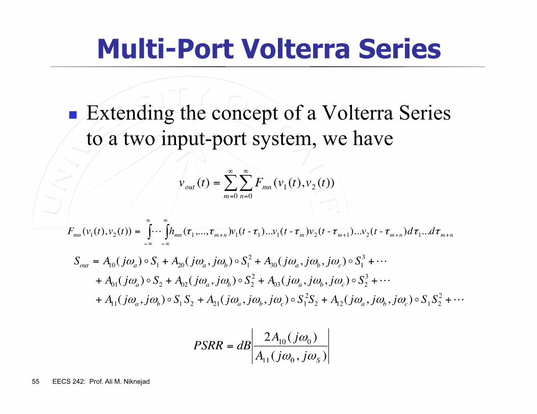
Multi-Port Volterra Series
Extending the concept of a Volterra Series to a two input-port system, we have
56 EECS 242: Prof. Ali M. Niknejad
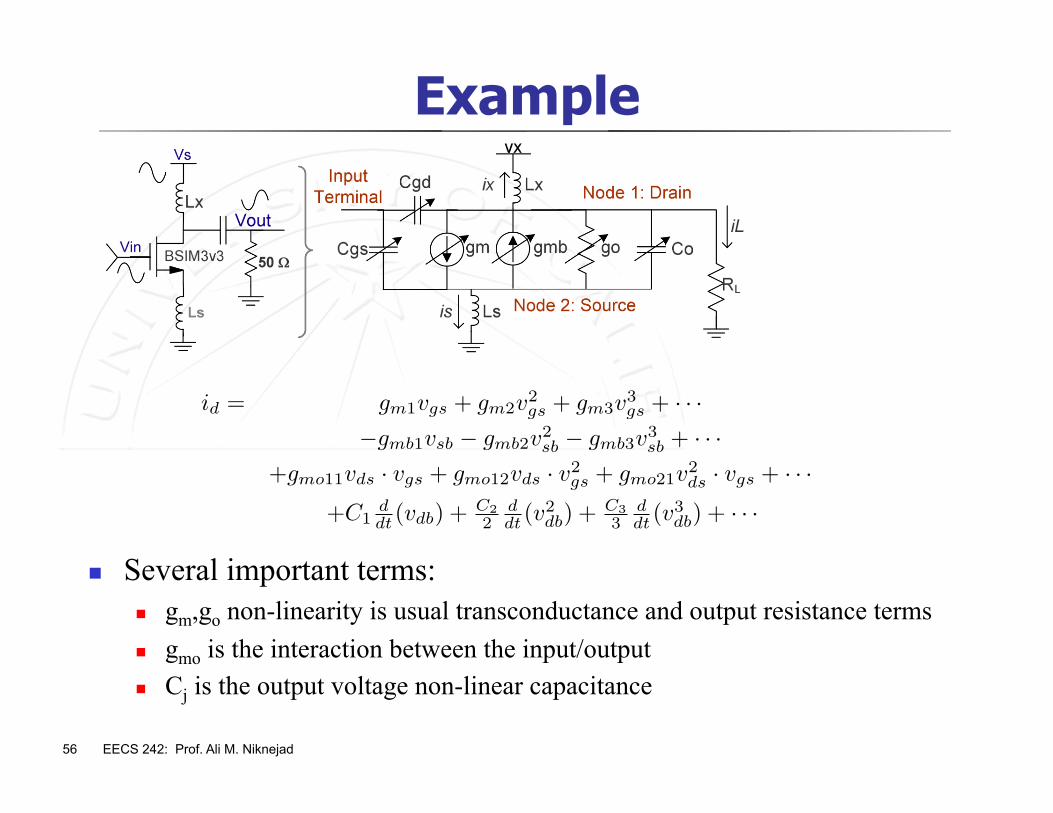
Example
Several important terms: gm,go non-linearity is usual transconductance and output resistance terms gmo is the interaction between the input/output Cj is the output voltage non-linear capacitance
id = gm1vgs + gm2v2gs + gm3v3
gs + · · ·!gmb1vsb ! gmb2v2
sb ! gmb3v3sb + · · ·
+gmo11vds · vgs + gmo12vds · v2gs + gmo21v2
ds · vgs + · · ·+C1
ddt (vdb) + C2
2ddt (v
2db) + C3
3ddt (v
3db) + · · ·
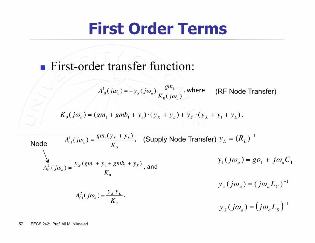
57 EECS 242: Prof. Ali M. Niknejad
First Order Terms
First-order transfer function:
Node (Supply Node Transfer)
(RF Node Transfer)
58 EECS 242: Prof. Ali M. Niknejad
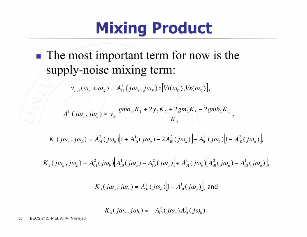
Mixing Product
The most important term for now is the supply-noise mixing term:
59 EECS 242: Prof. Ali M. Niknejad
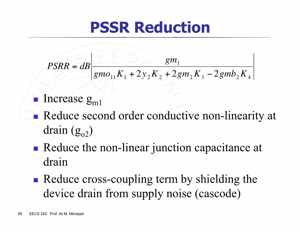
PSSR Reduction
Increase gm1
Reduce second order conductive non-linearity at drain (go2)
Reduce the non-linear junction capacitance at drain
Reduce cross-coupling term by shielding the device drain from supply noise (cascode)
60 EECS 242: Prof. Ali M. Niknejad
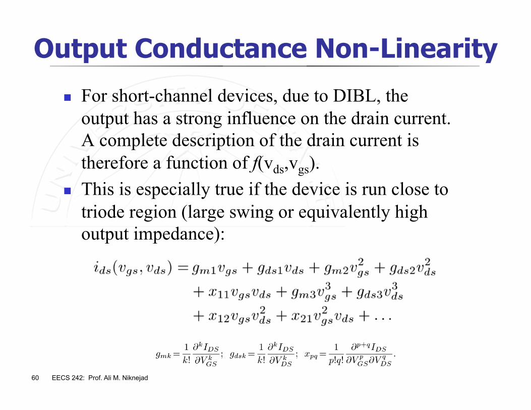
Output Conductance Non-Linearity
For short-channel devices, due to DIBL, the output has a strong influence on the drain current. A complete description of the drain current is therefore a function of f(vds,vgs).
This is especially true if the device is run close to triode region (large swing or equivalently high output impedance):
61 EECS 242: Prof. Ali M. Niknejad
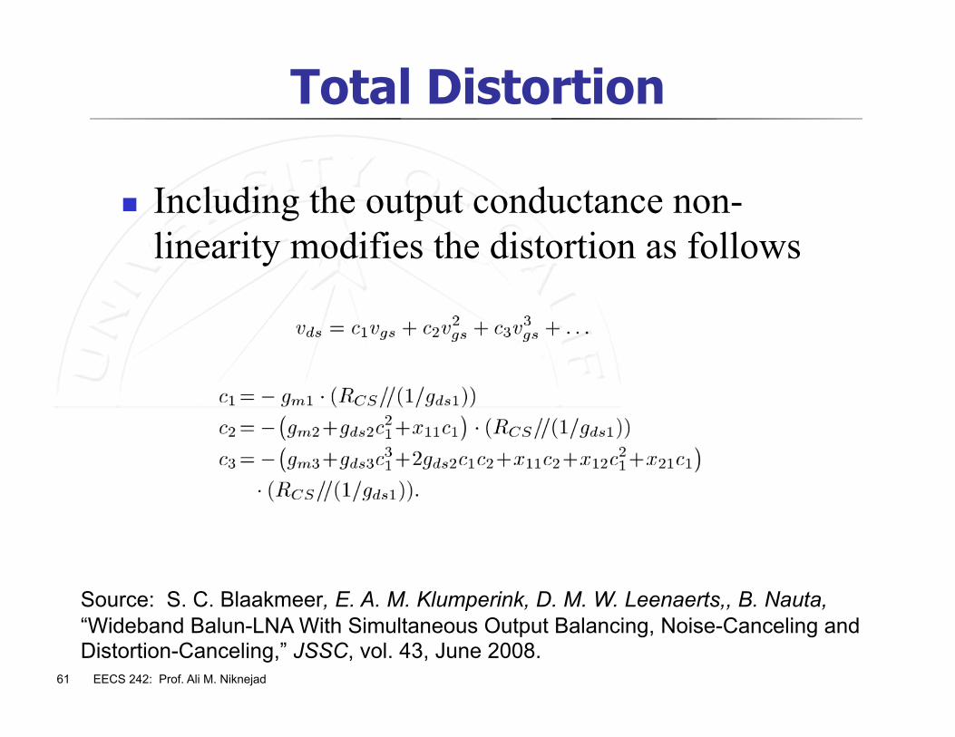
Total Distortion
Including the output conductance non-linearity modifies the distortion as follows
Source: S. C. Blaakmeer, E. A. M. Klumperink, D. M. W. Leenaerts,, B. Nauta, “Wideband Balun-LNA With Simultaneous Output Balancing, Noise-Canceling and Distortion-Canceling,” JSSC, vol. 43, June 2008.
62 EECS 242: Prof. Ali M. Niknejad
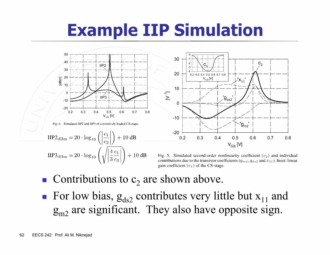
Example IIP Simulation
Contributions to c2 are shown above. For low bias, gds2 contributes very little but x11 and
gm2 are significant. They also have opposite sign.
63 EECS 242: Prof. Ali M. Niknejad
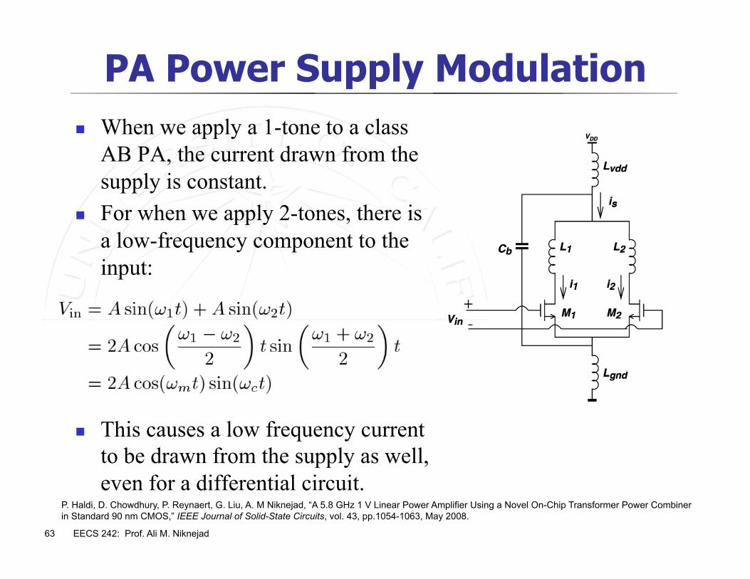
PA Power Supply Modulation When we apply a 1-tone to a class
AB PA, the current drawn from the supply is constant.
For when we apply 2-tones, there is a low-frequency component to the input:
This causes a low frequency current to be drawn from the supply as well, even for a differential circuit.
P. Haldi, D. Chowdhury, P. Reynaert, G. Liu, A. M Niknejad, “A 5.8 GHz 1 V Linear Power Amplifier Using a Novel On-Chip Transformer Power Combiner in Standard 90 nm CMOS,” IEEE Journal of Solid-State Circuits, vol. 43, pp.1054-1063, May 2008.
64 EECS 242: Prof. Ali M. Niknejad
Supply Current
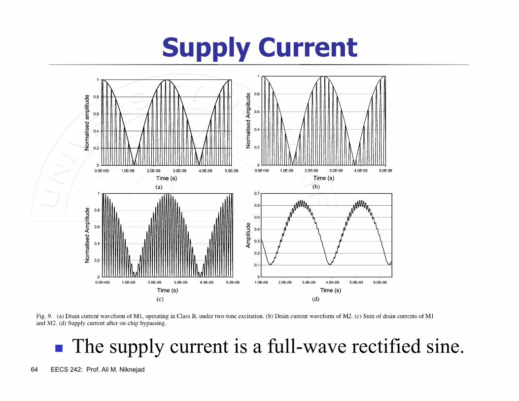
The supply current is a full-wave rectified sine.
65 EECS 242: Prof. Ali M. Niknejad
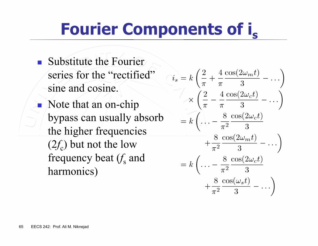
Fourier Components of is
Substitute the Fourier series for the “rectified” sine and cosine.
Note that an on-chip bypass can usually absorb the higher frequencies (2fc) but not the low frequency beat (fs and harmonics)
66 EECS 242: Prof. Ali M. Niknejad
Supply Ripple Voltage
The finite impedance of the supply means that the supply ripple has the following form. Assuming a multi-port Volterra description for the transistor results in:
67 EECS 242: Prof. Ali M. Niknejad
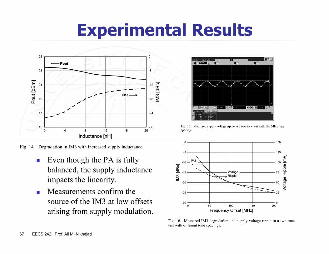
Experimental Results
Even though the PA is fully balanced, the supply inductance impacts the linearity.
Measurements confirm the source of the IM3 at low offsets arising from supply modulation.
68 EECS 242: Prof. Ali M. Niknejad
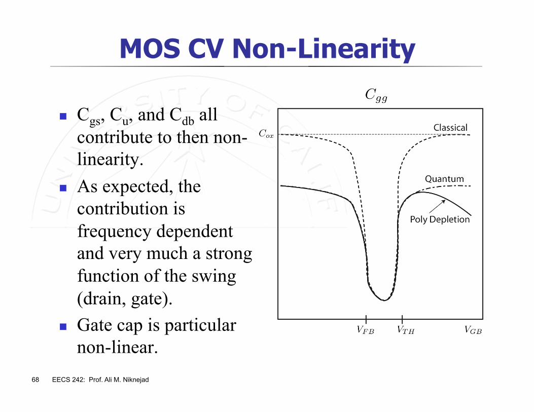
MOS CV Non-Linearity
Cgs, Cu, and Cdb all contribute to then non-linearity.
As expected, the contribution is frequency dependent and very much a strong function of the swing (drain, gate).
Gate cap is particular non-linear.
69 EECS 242: Prof. Ali M. Niknejad
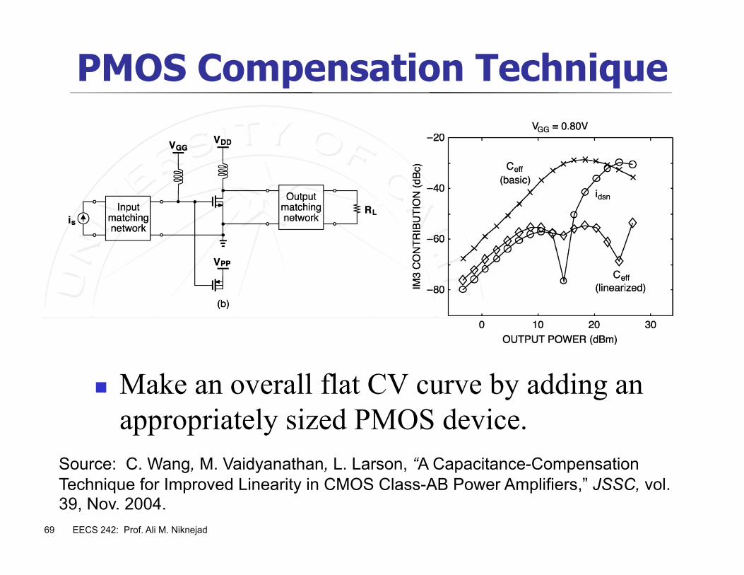
PMOS Compensation Technique
Make an overall flat CV curve by adding an appropriately sized PMOS device.
Source: C. Wang, M. Vaidyanathan, L. Larson, “A Capacitance-Compensation Technique for Improved Linearity in CMOS Class-AB Power Amplifiers,” JSSC, vol. 39, Nov. 2004.
70 EECS 242: Prof. Ali M. Niknejad
General References
Analysis and Design of Current-Commutating CMOS Mixers, Manolis Terrovitis Ph.D. dissertation, U.C. Berkeley 2001
Physical Background of MOS Model 11 (Level 1101), R. van Langevelde, A.J. Scholten and D.B.M. Klaassen, Philips Electronics N.V. 2003 (Unclassified Report)
UCB EECS 242 Class Notes, Ali M Niknejad, Spring 2002, Robert G. Meyer, Spring 1995.


![mlit.go.jp · 2019. 2. 1. · [235] [235) 123 [24.2] [240] [240] [24.3] [242 [242 [242] [242) [245 43] [242 (242 [242] [24.2] [ú.2] [242] [242 [240] [242] 27 087 087 [24.6] [24.6]](https://img.pdfslide.us/doc/110x75/613019b41ecc51586943e0fb/mlitgojp-2019-2-1-235-235-123-242-240-240-243-242-242-242.jpg)