Embed Size (px)
Citation preview
EE301 : Electronic Circuits
Unit 3 OPERATIONAL AMPLIFIERS
(OP-AMP) ( 08 : 06 )
LECTURER :
Engr. Muhammad muizz
COURSE LEARNING OUTCOME
• CLO2: explain correctly the basic principles of operational amplifier based on appropriate configurations.
Lecturer: engr. muhammad muizz bin mohd nawawi
3.1 Understand the general Op-Amp circuit Design
3.1.1 State the general design philosophy
3.1.2 Draw the symbol for Op-amp
3.1.3 Draw the block diagram an Op-Amp
a. Differential Amplifier
b. More stages Of Gain Amplifier
c. Push-Pull Amplifier
Lecturer: engr. muhammad muizz bin mohd nawawi
Operational Amplifier (Op-Amp)
• IC amplifier with very high gain. • It consists combination of many components
such as transistor, resistor in a silicone chip. • With a certain feedback, the op-amp can be used
to do multiplication, summation, subtraction, differentiation, integration and etc.
• An ideal amplifier has infinite Gain and Bandwidth when used in the Open-loop mode with typical d.c. gains of 100,000, or 100 dB.
• The basic Op-amp construction is of a 3-terminal device, 2-inputs and 1-output.
Lecturer: engr. muhammad muizz bin mohd nawawi

Op-Amp
• It operates from either a dual positive (+V) and an corresponding negative (-V) supply, or they can operate from a single DC supply voltage.
• The two main laws associated with the op- amp are that it has an infinite input impedance, (Zin =∞) resulting in "No current flowing into either of its two inputs" and zero input offset voltage "V1 = V2“.
Lecturer: engr. muhammad muizz bin mohd nawawi
Op-Amp
• An operational amplifier also has zero output impedance, (Z = 0).
• Op-amps sense the difference between the voltage signals applied to their two input terminals and then multiply it by some pre-determined Gain, (A).
• This Gain, (A) is often referred to as the amplifiers "Open-loop Gain".
Lecturer: engr. muhammad muizz bin mohd nawawi
Styled by : Sabariah Bt Bohanudin
Operational Amplifier
•It was originally adopted for a series of high performance DC amplifiers used in analog computers.
•It is used to perform mathematical operations applicable to analog computation such as summation, scaling, subtraction, integrating, etc. - essentially any feedback operation.
Lecturer: engr. muhammad muizz bin mohd nawawi
Styled by : Sabariah Bt Bohanudin
Operational Amplifier
• Its applications has become so widely diversified. •Op Amps are now used as a basic building block for; phase shifting, filtering, signal conditioning, multiplexing, detecting, etc.
Lecturer: engr. muhammad muizz bin mohd nawawi
Styled by : Sabariah Bt Bohanudin
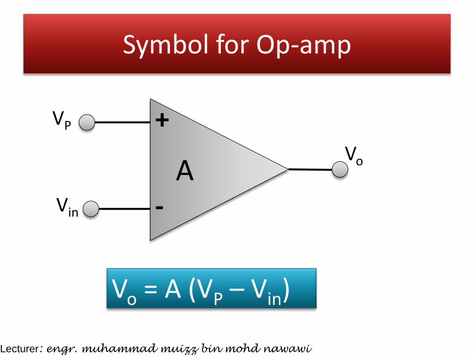
Symbol for Op-amp
Vo = A (VP – Vin)
Vo
VP
Vin
A
+
-
Lecturer: engr. muhammad muizz bin mohd nawawi
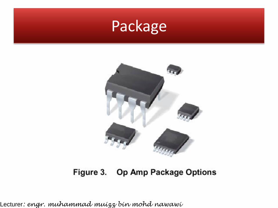
Package
Lecturer: engr. muhammad muizz bin mohd nawawi
Styled by : Sabariah Bt Bohanudin
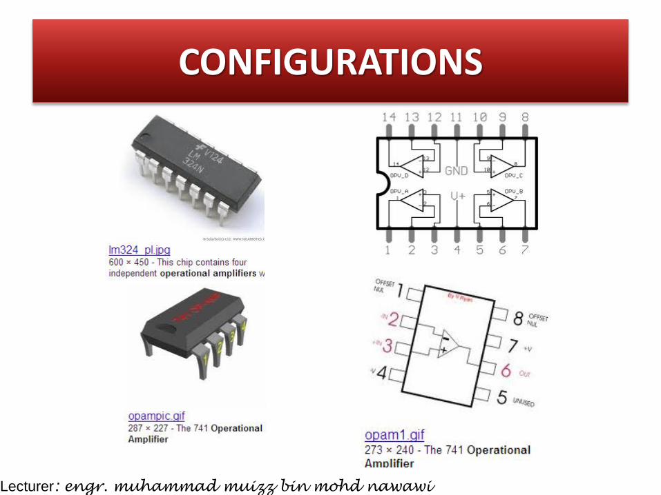
CONFIGURATIONS
Lecturer: engr. muhammad muizz bin mohd nawawi
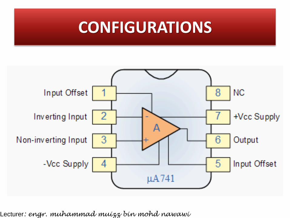
CONFIGURATIONS
Lecturer: engr. muhammad muizz bin mohd nawawi
3.2 Understand the Differential Amplifier
Explain a DC analysis of differential amplifier
Determine input bias current, input offset current and input offset voltage.
Define common-mode gain and common-mode rejection ratio
Lecturer: engr. muhammad muizz bin mohd nawawi
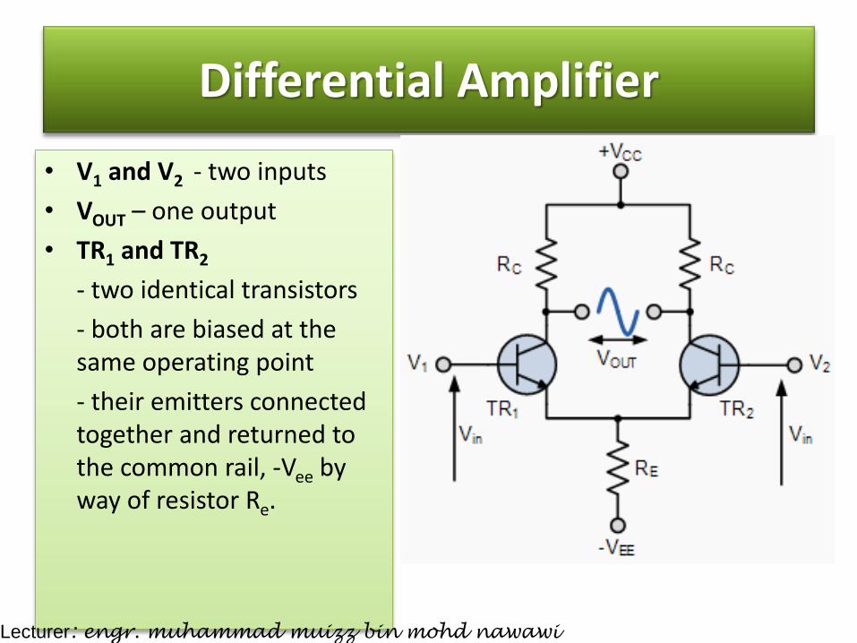
Differential Amplifier
• V1 and V2 - two inputs
• VOUT – one output
• TR1 and TR2
- two identical transistors
- both are biased at the same operating point
- their emitters connected together and returned to the common rail, -Vee by way of resistor Re.
Lecturer: engr. muhammad muizz bin mohd nawawi
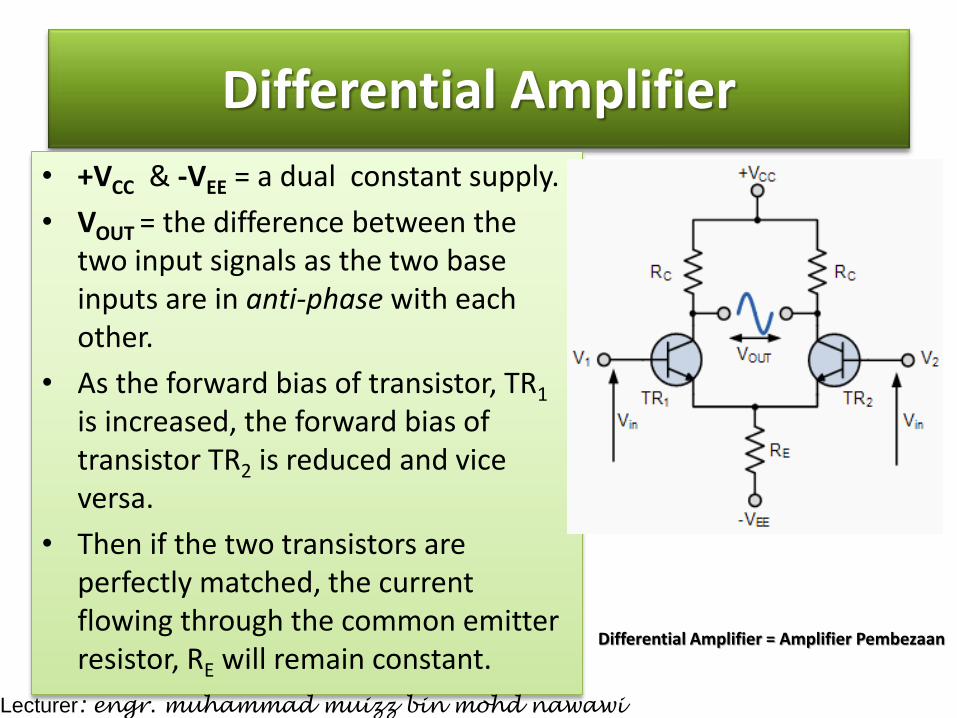
Differential Amplifier
• +VCC & -VEE = a dual constant supply.
• VOUT = the difference between the two input signals as the two base inputs are in anti-phase with each other.
• As the forward bias of transistor, TR1 is increased, the forward bias of transistor TR2 is reduced and vice versa.
• Then if the two transistors are perfectly matched, the current flowing through the common emitter resistor, RE will remain constant.
Differential Amplifier = Amplifier Pembezaan
Lecturer: engr. muhammad muizz bin mohd nawawi
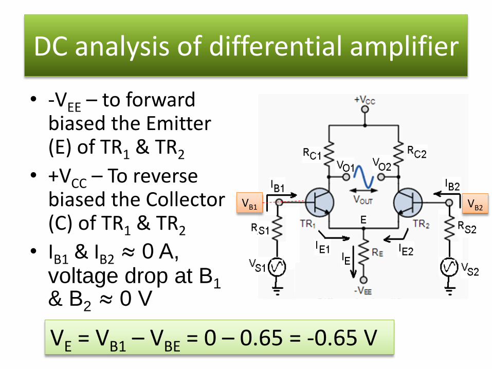
DC analysis of differential amplifier
• -VEE – to forward biased the Emitter (E) of TR1 & TR2
• +VCC – To reverse biased the Collector (C) of TR1 & TR2
• IB1 & IB2 ≈ 0 A, voltage drop at B1 & B2 ≈ 0 V
VE = VB1 – VBE = 0 – 0.65 = -0.65 V
VB1 VB2
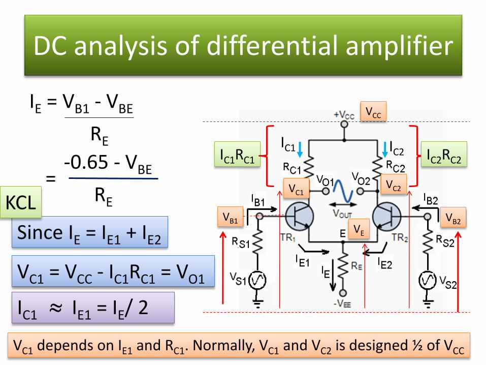
DC analysis of differential amplifier
IE = VB1 - VBE
RE
-0.65 - VBE =
RE
Since IE = IE1 + IE2
KCL VB1 VB2
VC1 VC2
VE
VCC
IC1 IC2 IC1RC1 IC2RC2
IC1 ≈ IE1 = IE/ 2
VC1 = VCC - IC1RC1 = VO1
VC1 depends on IE1 and RC1. Normally, VC1 and VC2 is designed ½ of VCC
DC offset voltage
• In ideal op-amp, when there is no input signal, Vout = 0 V.
• In practical, when power supply is given to the circuit, there is DC voltage exist at Vout even though Vin = 0 V. This condition is called DC offset.
• There are 3 factors cause DC offset voltage;
1. input bias current, IB
2. input offset current , Iio
3. input offset voltage.
Lecturer: engr. muhammad muizz bin mohd nawawi
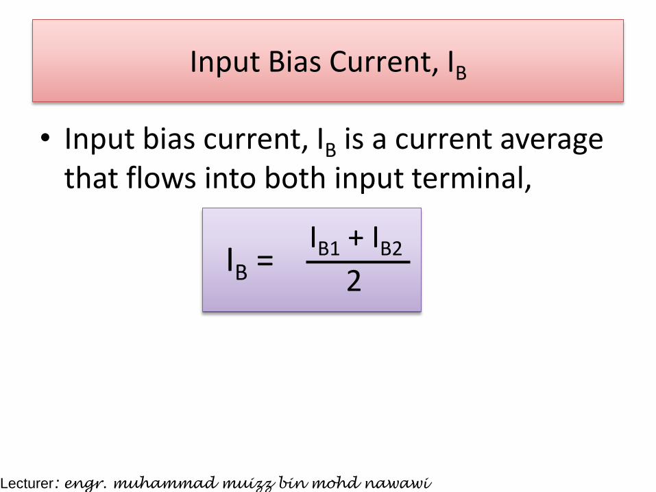
Input Bias Current, IB
• Input bias current, IB is a current average that flows into both input terminal,
IB1 + IB2
2 IB =
Lecturer: engr. muhammad muizz bin mohd nawawi
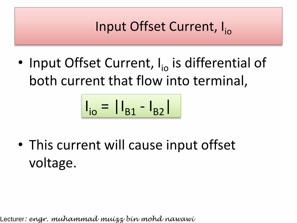
Input Offset Current, Iio
• Input Offset Current, Iio is differential of both current that flow into terminal,
• This current will cause input offset voltage.
Iio = |IB1 - IB2|
Lecturer: engr. muhammad muizz bin mohd nawawi
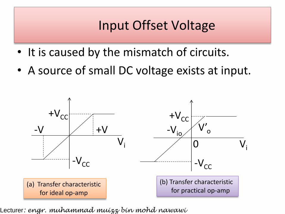
Input Offset Voltage
• It is caused by the mismatch of circuits.
• A source of small DC voltage exists at input.
+VCC
-VCC
+V Vi
-V
+VCC
-VCC
0 Vi
-Vio V’o
(a) Transfer characteristic for ideal op-amp
(b) Transfer characteristic for practical op-amp
Lecturer: engr. muhammad muizz bin mohd nawawi
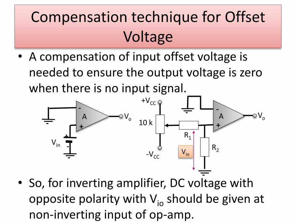
Compensation technique for Offset Voltage
• A compensation of input offset voltage is needed to ensure the output voltage is zero when there is no input signal.
• So, for inverting amplifier, DC voltage with opposite polarity with Vio should be given at non-inverting input of op-amp.
Vo
Vin
A -
+ + -
A Vo
-
+
R2
R1
10 k
+VCC
-VCC Vio
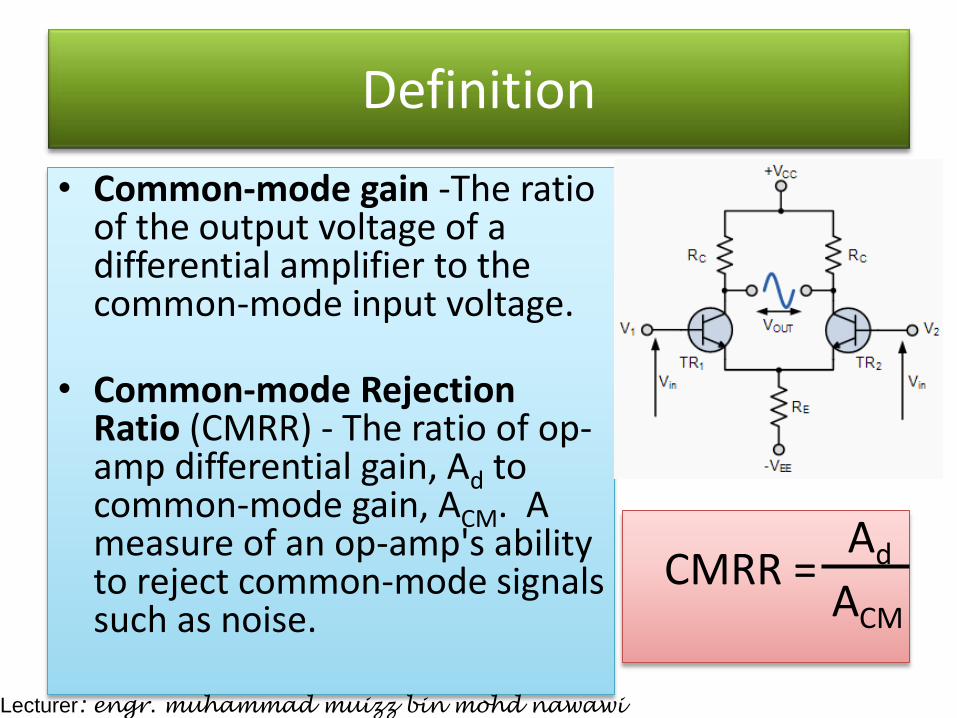
Definition
• Common-mode gain -The ratio of the output voltage of a differential amplifier to the common-mode input voltage.
• Common-mode Rejection Ratio (CMRR) - The ratio of op-amp differential gain, Ad to common-mode gain, ACM. A measure of an op-amp's ability to reject common-mode signals such as noise.
CMRR = Ad
ACM
Lecturer: engr. muhammad muizz bin mohd nawawi
Common Mode Rejection Ratio
• Ideal Op Amp - if an identical signal is applied to both the inverting and non-inverting inputs there should no change to the output.
• However, in real amplifiers there is always some variation and the ratio of the change to the output voltage with regards to the change in the common mode input voltage is called the Common Mode Rejection Ratio or CMRR.
Lecturer: engr. muhammad muizz bin mohd nawawi
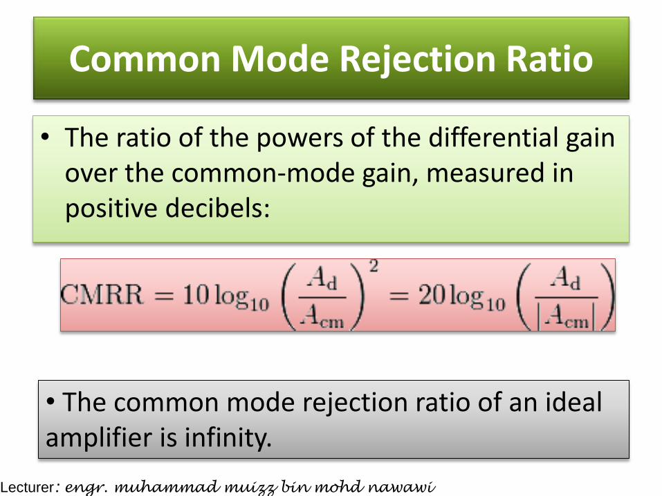
• The ratio of the powers of the differential gain over the common-mode gain, measured in positive decibels:
Common Mode Rejection Ratio
• The common mode rejection ratio of an ideal amplifier is infinity.
Lecturer: engr. muhammad muizz bin mohd nawawi
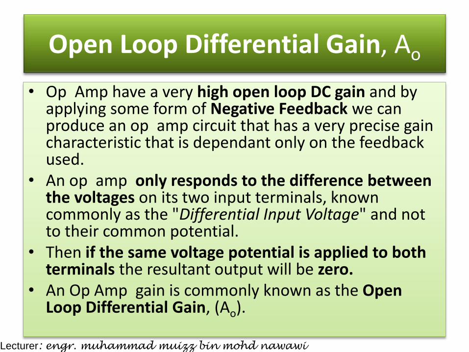
Open Loop Differential Gain, Ao
• Op Amp have a very high open loop DC gain and by applying some form of Negative Feedback we can produce an op amp circuit that has a very precise gain characteristic that is dependant only on the feedback used.
• An op amp only responds to the difference between the voltages on its two input terminals, known commonly as the "Differential Input Voltage" and not to their common potential.
• Then if the same voltage potential is applied to both terminals the resultant output will be zero.
• An Op Amp gain is commonly known as the Open Loop Differential Gain, (Ao).
Lecturer: engr. muhammad muizz bin mohd nawawi
3.3 Understand more stages of gain amplifier
• 3.3.1 Draw complimentary amplifier.
Lecturer: engr. muhammad muizz bin mohd nawawi
3.4 Understand the push-pull Amplifier
3.4.1 Draw push-pull amplifier circuit
3.4.2 Explain briefly the operation of push-pull amplifier.
Lecturer: engr. muhammad muizz bin mohd nawawi
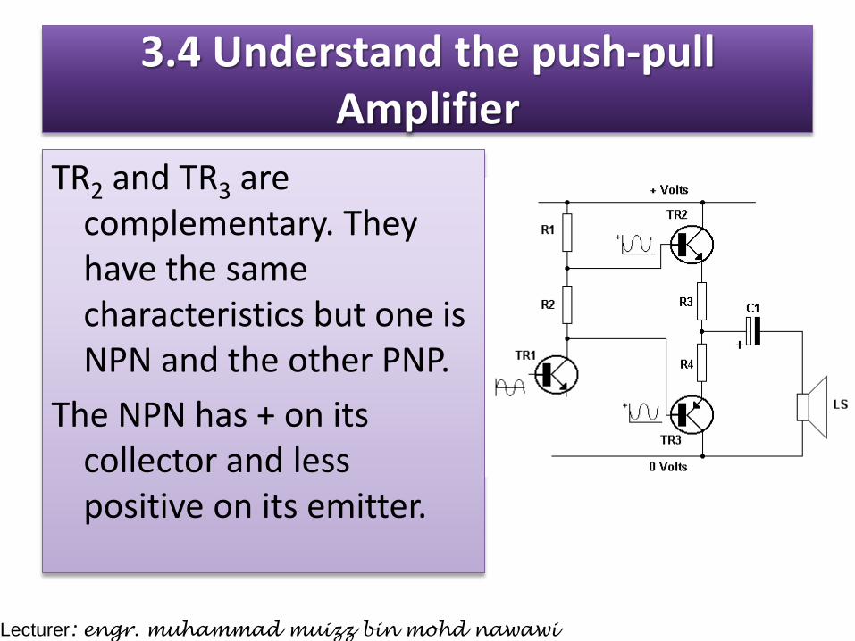
3.4 Understand the push-pull Amplifier
TR2 and TR3 are complementary. They have the same characteristics but one is NPN and the other PNP.
The NPN has + on its collector and less positive on its emitter.
Lecturer: engr. muhammad muizz bin mohd nawawi
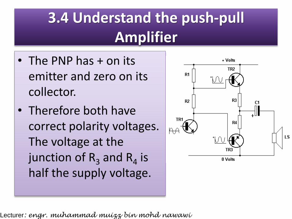
3.4 Understand the push-pull Amplifier
• The PNP has + on its emitter and zero on its collector.
• Therefore both have correct polarity voltages. The voltage at the junction of R3 and R4 is half the supply voltage.
Lecturer: engr. muhammad muizz bin mohd nawawi
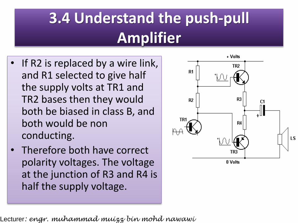
3.4 Understand the push-pull Amplifier
• If R2 is replaced by a wire link, and R1 selected to give half the supply volts at TR1 and TR2 bases then they would both be biased in class B, and both would be non conducting.
• Therefore both have correct polarity voltages. The voltage at the junction of R3 and R4 is half the supply voltage.
Lecturer: engr. muhammad muizz bin mohd nawawi

3.4 Understand the push-pull Amplifier
• 3.4.1 Draw push-pull amplifier circuit
• 3.4.2 Explain briefly the operation of push-pull amplifier.
Lecturer: engr. muhammad muizz bin mohd nawawi
3.4 Understand the push-pull Amplifier
• 3.4.1 Draw push-pull amplifier circuit
• 3.4.2 Explain briefly the operation of push-pull amplifier.
Lecturer: engr. muhammad muizz bin mohd nawawi
Ideal Operational Amplifier
Lecturer: engr. muhammad muizz bin mohd nawawi
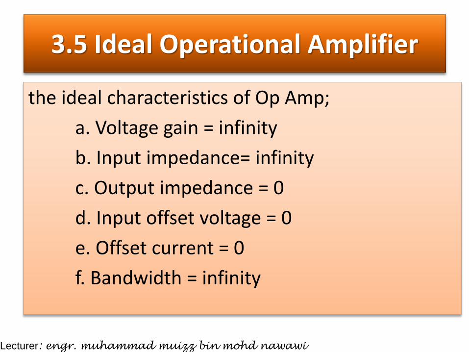
3.5 Ideal Operational Amplifier
the ideal characteristics of Op Amp;
a. Voltage gain = infinity
b. Input impedance= infinity
c. Output impedance = 0
d. Input offset voltage = 0
e. Offset current = 0
f. Bandwidth = infinity
Lecturer: engr. muhammad muizz bin mohd nawawi
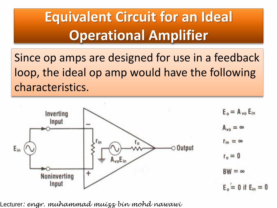
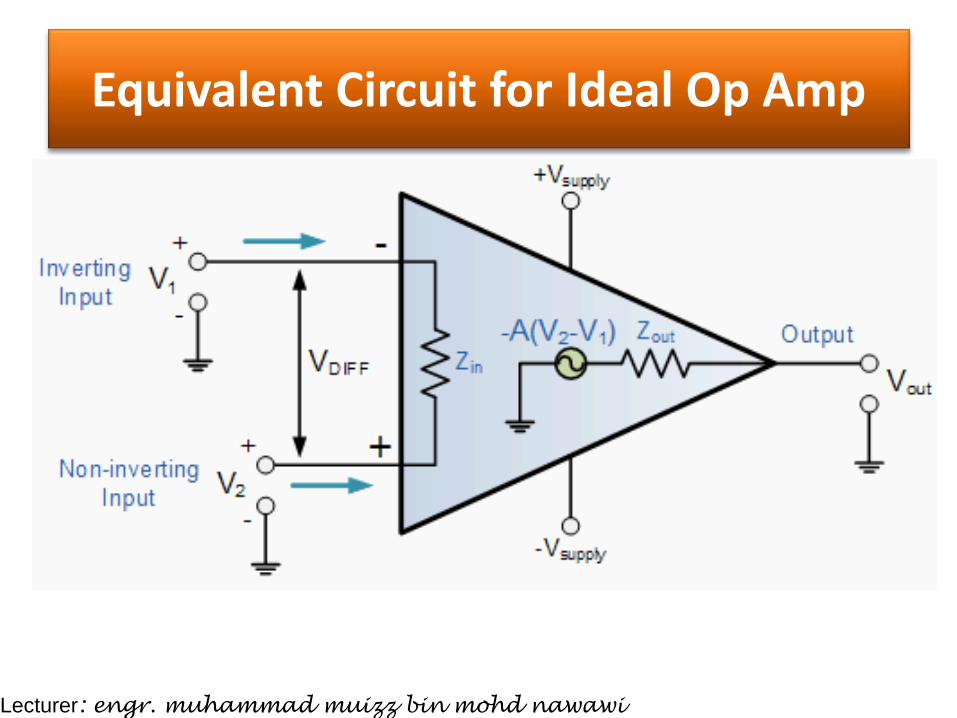
Equivalent Circuit for an Ideal Operational Amplifier
Since op amps are designed for use in a feedback loop, the ideal op amp would have the following characteristics.
Lecturer: engr. muhammad muizz bin mohd nawawi
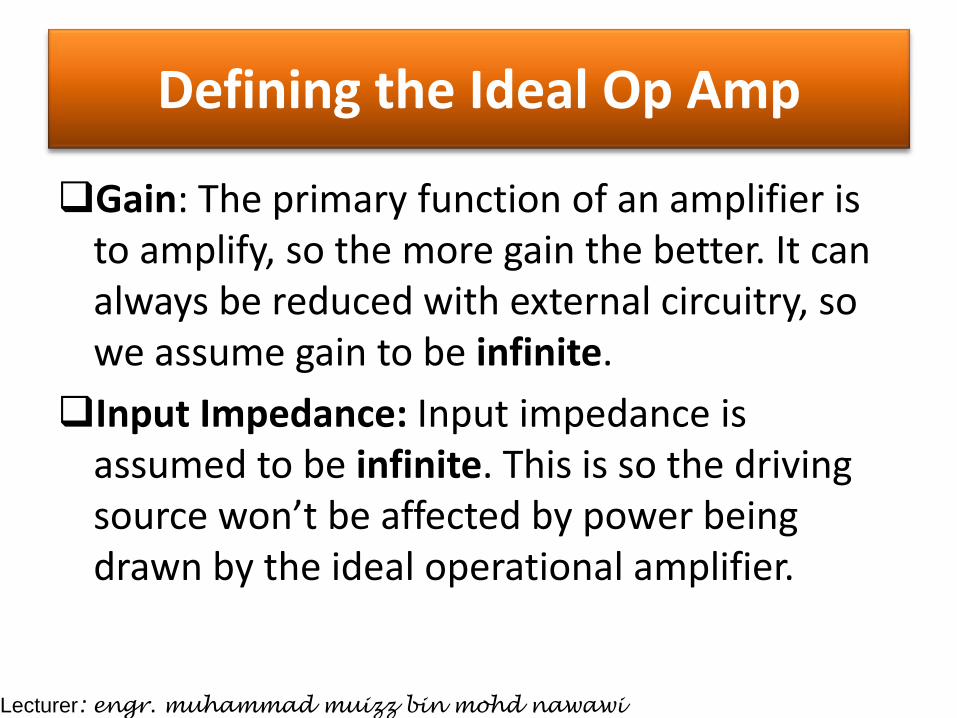
Defining the Ideal Op Amp
Gain: The primary function of an amplifier is to amplify, so the more gain the better. It can always be reduced with external circuitry, so we assume gain to be infinite.
Input Impedance: Input impedance is assumed to be infinite. This is so the driving source won’t be affected by power being drawn by the ideal operational amplifier.
Lecturer: engr. muhammad muizz bin mohd nawawi
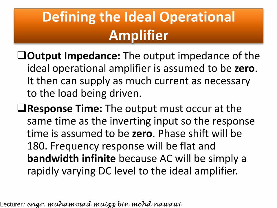
Defining the Ideal Operational Amplifier
Output Impedance: The output impedance of the ideal operational amplifier is assumed to be zero. It then can supply as much current as necessary to the load being driven.
Response Time: The output must occur at the same time as the inverting input so the response time is assumed to be zero. Phase shift will be 180. Frequency response will be flat and bandwidth infinite because AC will be simply a rapidly varying DC level to the ideal amplifier.
Lecturer: engr. muhammad muizz bin mohd nawawi
Defining the Ideal Operational Amplifier
Offset: The amplifier output will be zero when a zero signal appears between the inverting and non-inverting inputs.
Lecturer: engr. muhammad muizz bin mohd nawawi
Equivalent Circuit for Ideal Op Amp
Lecturer: engr. muhammad muizz bin mohd nawawi
AvVin
Vout Vin Zin= ∞
Av= ∞
Zout= 0
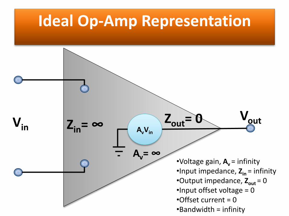
Ideal Op-Amp Representation
•Voltage gain, Av = infinity •Input impedance, Zin = infinity •Output impedance, Zout = 0 •Input offset voltage = 0 •Offset current = 0 •Bandwidth = infinity
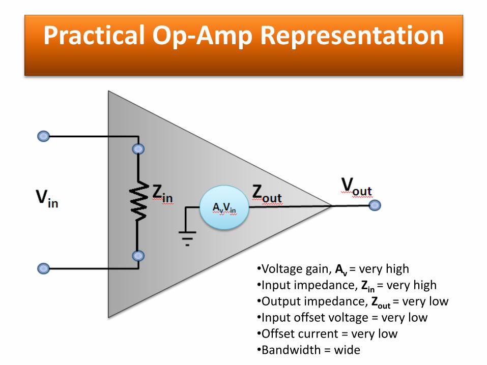
Practical Op-Amp Representation
•Voltage gain, Av = very high •Input impedance, Zin = very high •Output impedance, Zout = very low •Input offset voltage = very low •Offset current = very low •Bandwidth = wide
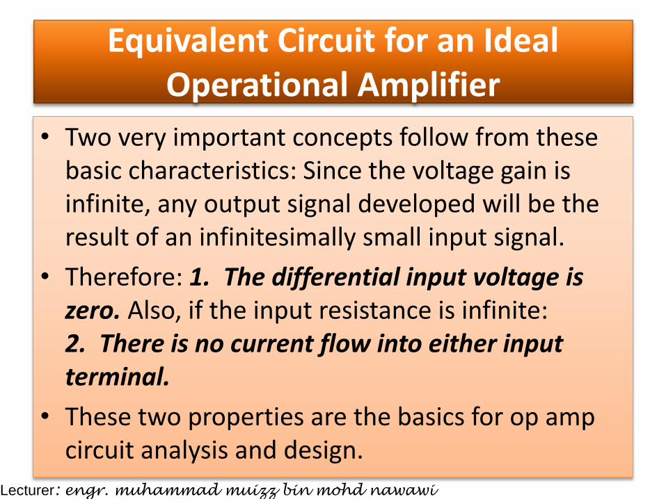
• Two very important concepts follow from these basic characteristics: Since the voltage gain is infinite, any output signal developed will be the result of an infinitesimally small input signal.
• Therefore: 1. The differential input voltage is zero. Also, if the input resistance is infinite: 2. There is no current flow into either input terminal.
• These two properties are the basics for op amp circuit analysis and design.
Equivalent Circuit for an Ideal Operational Amplifier
Lecturer: engr. muhammad muizz bin mohd nawawi
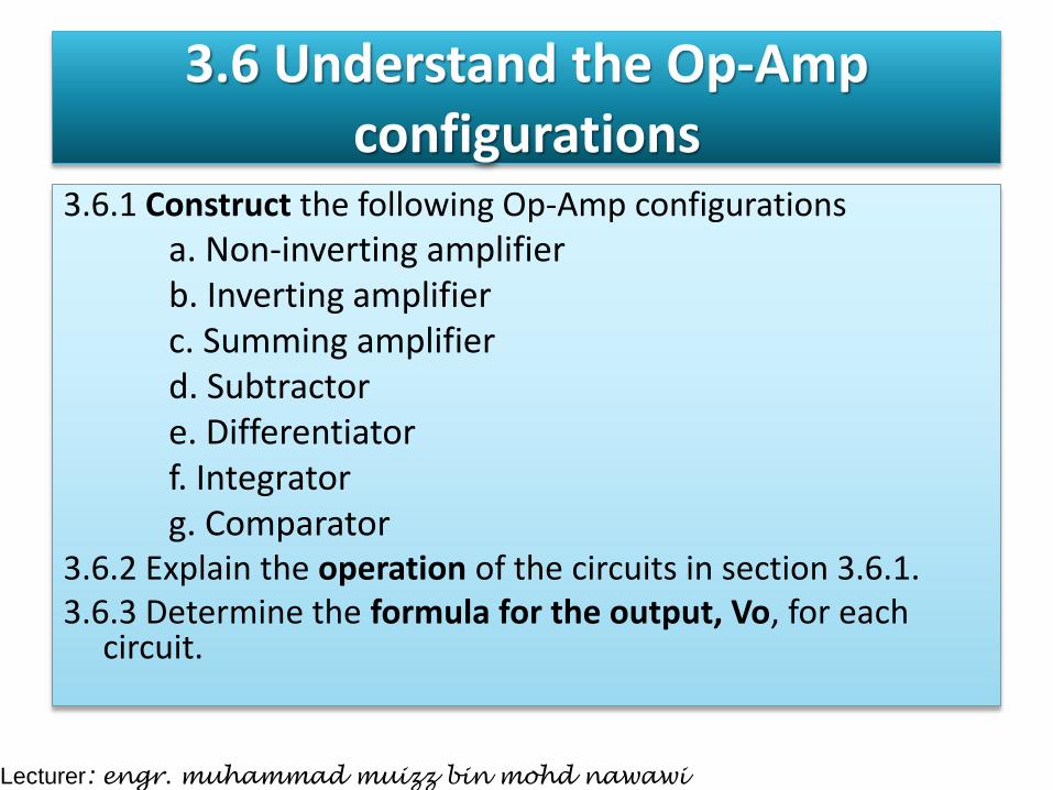
3.6 Understand the Op-Amp configurations
3.6.1 Construct the following Op-Amp configurations a. Non-inverting amplifier b. Inverting amplifier c. Summing amplifier d. Subtractor e. Differentiator f. Integrator g. Comparator
3.6.2 Explain the operation of the circuits in section 3.6.1. 3.6.3 Determine the formula for the output, Vo, for each
circuit.
Lecturer: engr. muhammad muizz bin mohd nawawi
Basic configuration
• Op-amps can be connected into two basic configurations, Inverting and Non-inverting.
Lecturer: engr. muhammad muizz bin mohd nawawi
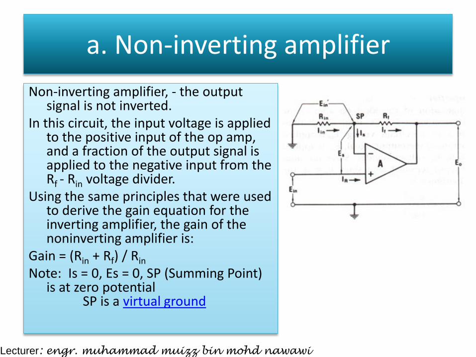
a. Non-inverting amplifier
Non-inverting amplifier, - the output signal is not inverted.
In this circuit, the input voltage is applied to the positive input of the op amp, and a fraction of the output signal is applied to the negative input from the Rf - Rin voltage divider.
Using the same principles that were used to derive the gain equation for the inverting amplifier, the gain of the noninverting amplifier is:
Gain = (Rin + Rf) / Rin
Note: Is = 0, Es = 0, SP (Summing Point) is at zero potential SP is a virtual ground
Lecturer: engr. muhammad muizz bin mohd nawawi
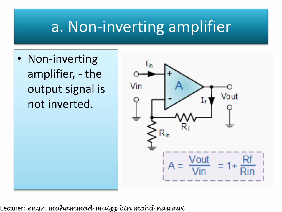
a. Non-inverting amplifier
• Non-inverting amplifier, - the output signal is not inverted.
Lecturer: engr. muhammad muizz bin mohd nawawi
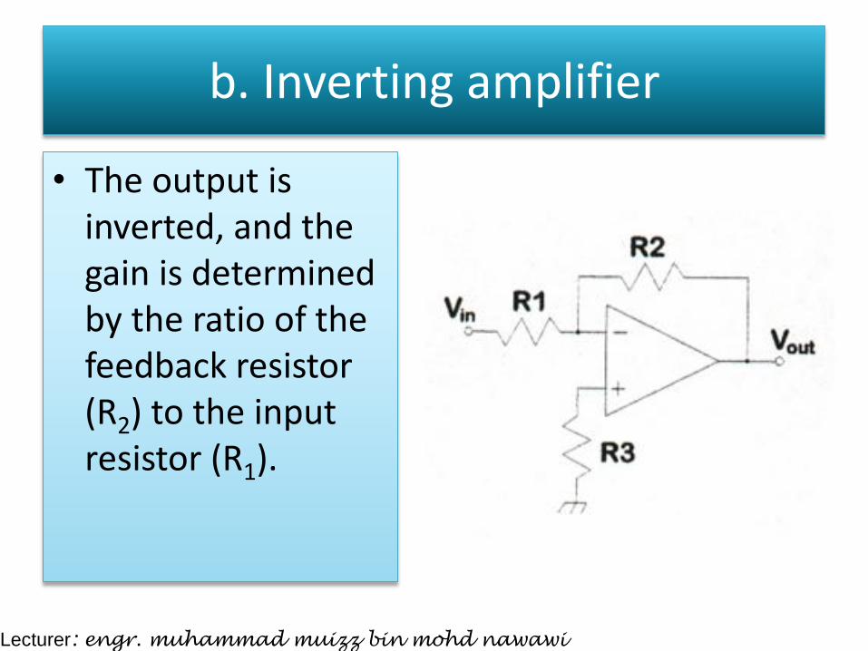
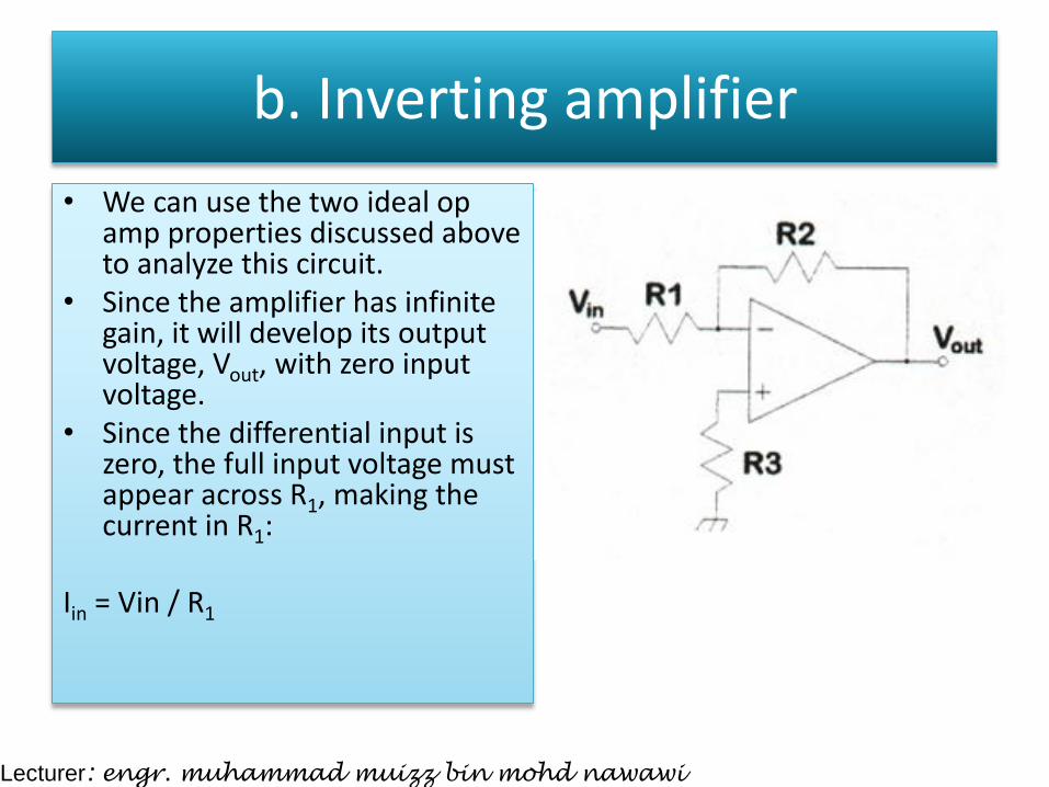
b. Inverting amplifier
• The output is inverted, and the gain is determined by the ratio of the feedback resistor (R2) to the input resistor (R1).
Lecturer: engr. muhammad muizz bin mohd nawawi
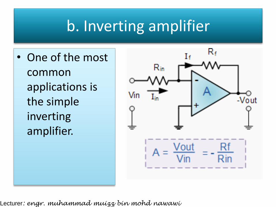
b. Inverting amplifier
• One of the most common applications is the simple inverting amplifier.
Lecturer: engr. muhammad muizz bin mohd nawawi
b. Inverting amplifier
• We can use the two ideal op amp properties discussed above to analyze this circuit.
• Since the amplifier has infinite gain, it will develop its output voltage, Vout, with zero input voltage.
• Since the differential input is zero, the full input voltage must appear across R1, making the current in R1:
Iin = Vin / R1
Lecturer: engr. muhammad muizz bin mohd nawawi
b. Inverting amplifier
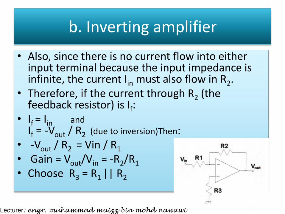
• Also, since there is no current flow into either input terminal because the input impedance is infinite, the current Iin must also flow in R2.
• Therefore, if the current through R2 (the feedback resistor) is If:
• If = Iin and If = -Vout / R2 (due to inversion)Then:
• -Vout / R2 = Vin / R1 • Gain = Vout/Vin = -R2/R1 • Choose R3 = R1 || R2
Lecturer: engr. muhammad muizz bin mohd nawawi
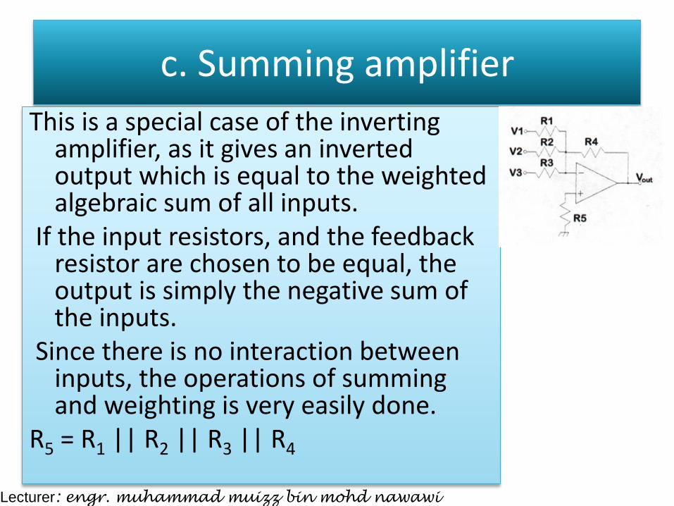
c. Summing amplifier
This is a special case of the inverting amplifier, as it gives an inverted output which is equal to the weighted algebraic sum of all inputs.
If the input resistors, and the feedback resistor are chosen to be equal, the output is simply the negative sum of the inputs.
Since there is no interaction between inputs, the operations of summing and weighting is very easily done.
R5 = R1 || R2 || R3 || R4
Lecturer: engr. muhammad muizz bin mohd nawawi
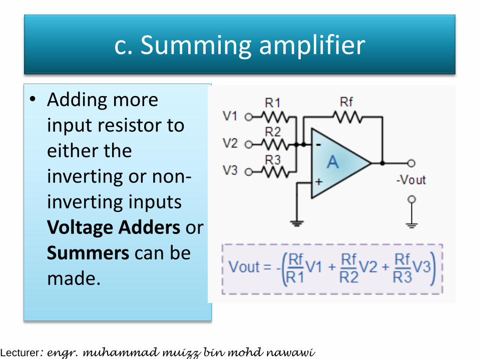
c. Summing amplifier
• Adding more input resistor to either the inverting or non-inverting inputs Voltage Adders or Summers can be made.
Lecturer: engr. muhammad muizz bin mohd nawawi
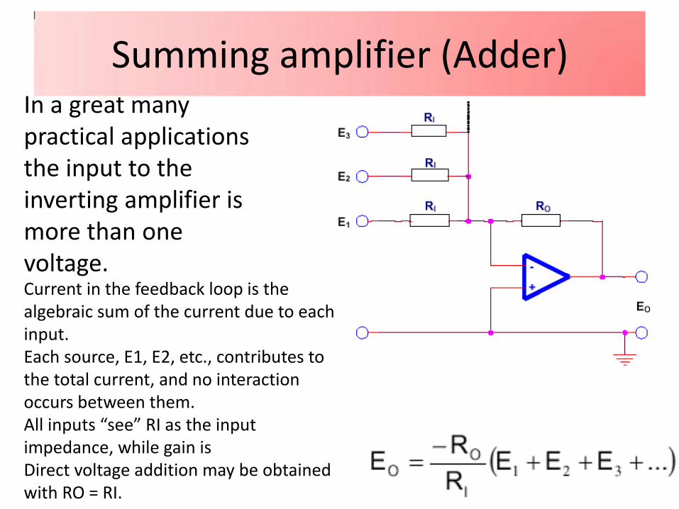
Summing amplifier (Adder) In a great many practical applications the input to the inverting amplifier is more than one voltage. Current in the feedback loop is the algebraic sum of the current due to each input. Each source, E1, E2, etc., contributes to the total current, and no interaction occurs between them. All inputs “see” RI as the input impedance, while gain is Direct voltage addition may be obtained with RO = RI.
e. Differentiator
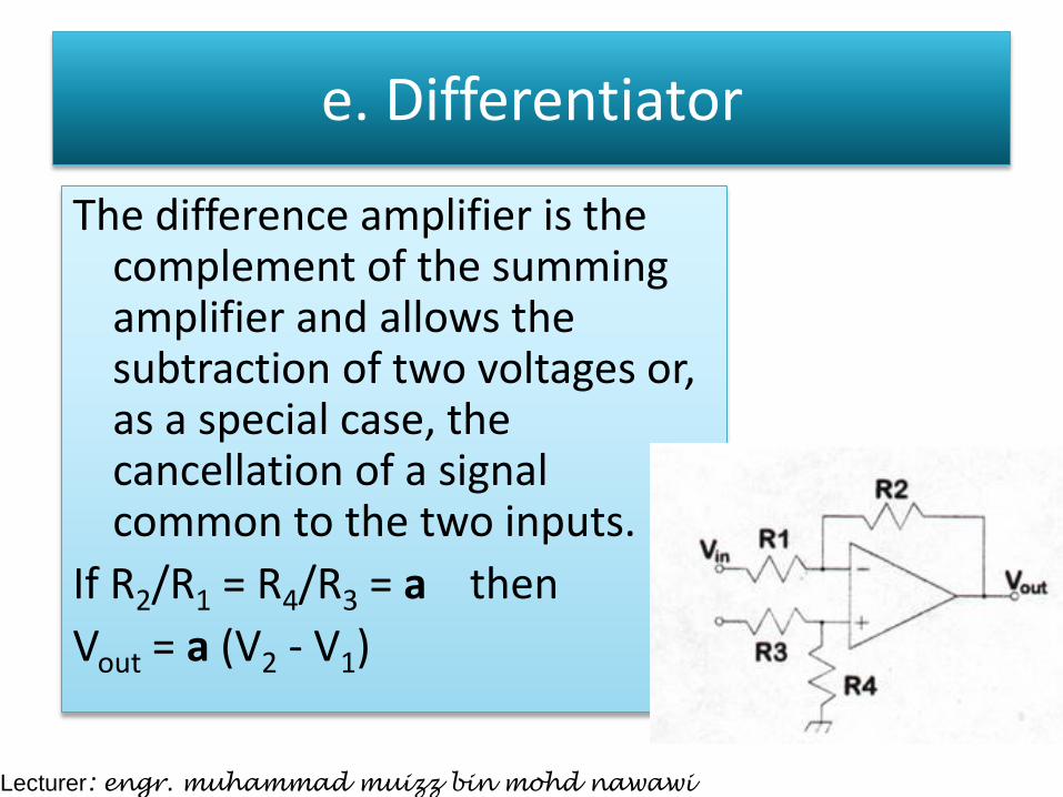
The difference amplifier is the complement of the summing amplifier and allows the subtraction of two voltages or, as a special case, the cancellation of a signal common to the two inputs.
If R2/R1 = R4/R3 = a then
Vout = a (V2 - V1)
Lecturer: engr. muhammad muizz bin mohd nawawi
e. Differential Op Amp
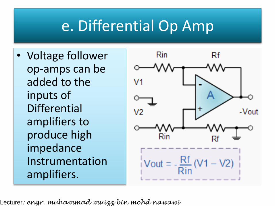
• Voltage follower op-amps can be added to the inputs of Differential amplifiers to produce high impedance Instrumentation amplifiers.
Lecturer: engr. muhammad muizz bin mohd nawawi
f. Integrator
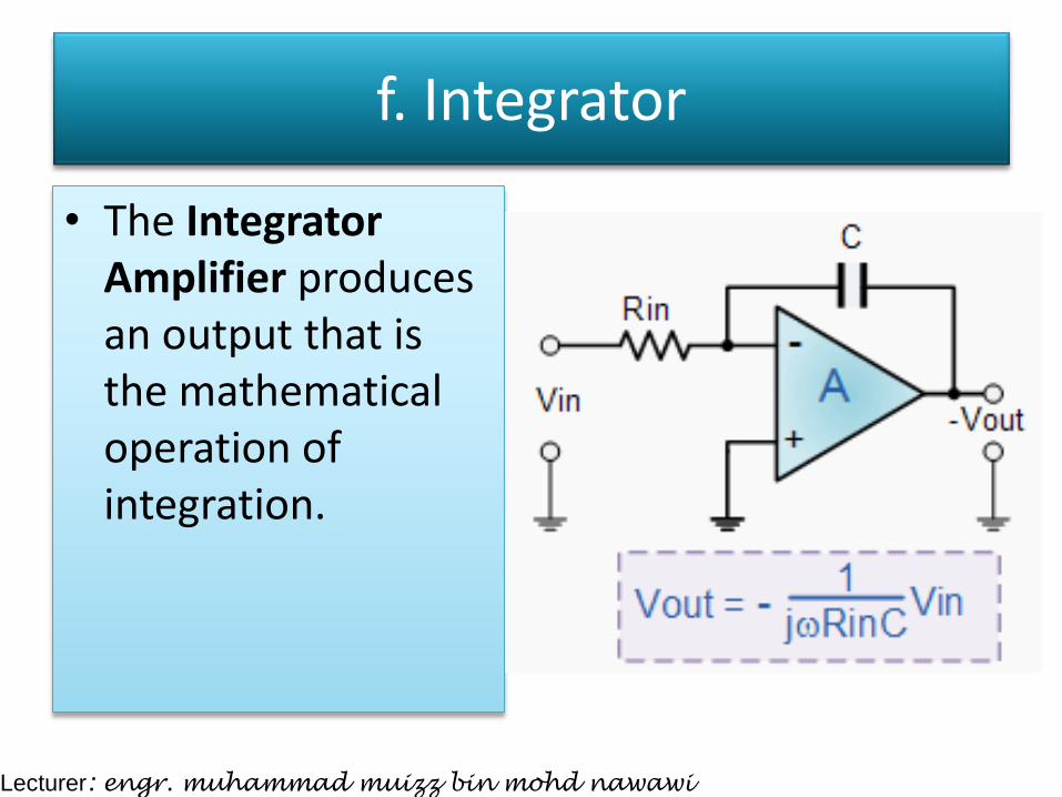
• The Integrator Amplifier produces an output that is the mathematical operation of integration.
Lecturer: engr. muhammad muizz bin mohd nawawi
Integrator and Differentiator Amplifiers - Disadvantages
• Both the Integrator and Differentiator Amplifiers have a resistor and capacitor connected across the op-amp and are affected by its RC time constant.
• In their basic form, Differentiator Amplifiers suffer from instability and noise but additional components can be added to reduce the overall closed-loop gain.
Lecturer: engr. muhammad muizz bin mohd nawawi
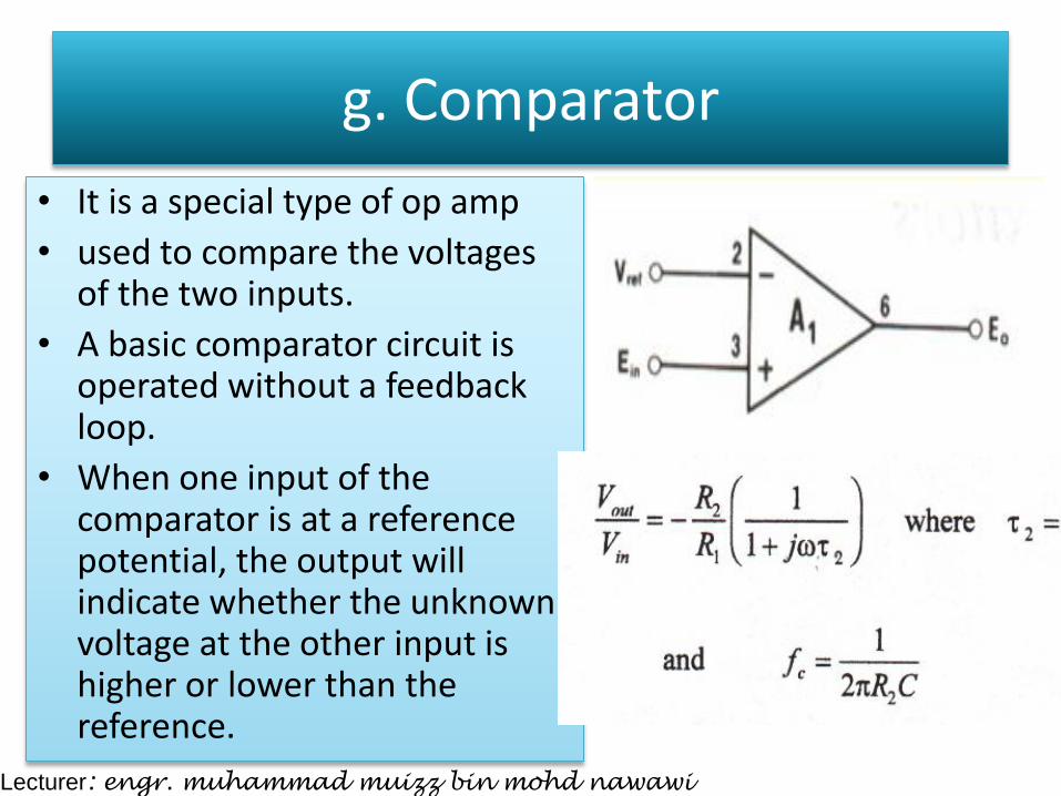
g. Comparator
• It is a special type of op amp
• used to compare the voltages of the two inputs.
• A basic comparator circuit is operated without a feedback loop.
• When one input of the comparator is at a reference potential, the output will indicate whether the unknown voltage at the other input is higher or lower than the reference.
Lecturer: engr. muhammad muizz bin mohd nawawi
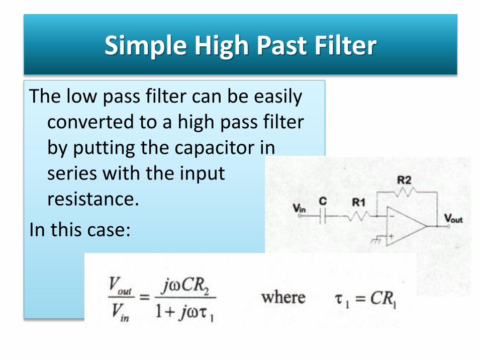
Simple High Past Filter
The low pass filter can be easily converted to a high pass filter by putting the capacitor in series with the input resistance.
In this case:
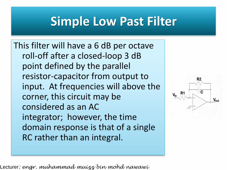
Simple Low Past Filter
This filter will have a 6 dB per octave roll-off after a closed-loop 3 dB point defined by the parallel resistor-capacitor from output to input. At frequencies will above the corner, this circuit may be considered as an AC integrator; however, the time domain response is that of a single RC rather than an integral.
Lecturer: engr. muhammad muizz bin mohd nawawi