Embed Size (px)
Citation preview
EECS 247 Lecture 15: Data Converters- DAC Design & Intro. to ADCs © 2010 Page 1
EE247
Lecture 15
• D/A converters– Practical aspects of current-switched DACs
(continued)
– Segmented current-switched DACs– DAC dynamic non-idealities
– DAC design considerations
– Self calibration techniques• Current copiers
• Dynamic element matching
– DAC reconstruction filter
• A/D converter introduction
EECS 247 Lecture 15: Data Converters- DAC Design & Intro. to ADCs © 2010 Page 2
Summary Last Lecture
D/A converter architectures:– Resistor string DAC
– Serial charge redistribution DAC
– Parallel charge scaling DAC
– Combination of resistor string (MSB) & binary weighted charge scaling (LSB)
– Current source DAC• Unit element
• Binary weighted
• Static performance
– Component matching-systematic & random errors• Component random variations Gaussian pdf
• INL for both unit-element & binary weight DAC: sINL= se x2B/2-1
• DNL for unit-element: sDNL= se
• DNL for binary-weighted sDNL= se x2B/2
EECS 247 Lecture 15: Data Converters- DAC Design & Intro. to ADCs © 2010 Page 3
INL & DNL for Binary Weighted DAC
• INL same as for unit
element DAC
• DNL depends on transition
–Example:
0 to 1sDNL2 = s(dI/I)
2
1 to 2 sDNL2 = 3s(dI/I)
2
• Consider MSB transition:
0111 … 1000 …
4 Iref Iref
Iout
2Iref2B-1 Iref
……………
EECS 247 Lecture 15: Data Converters- DAC Design & Intro. to ADCs © 2010 Page 4
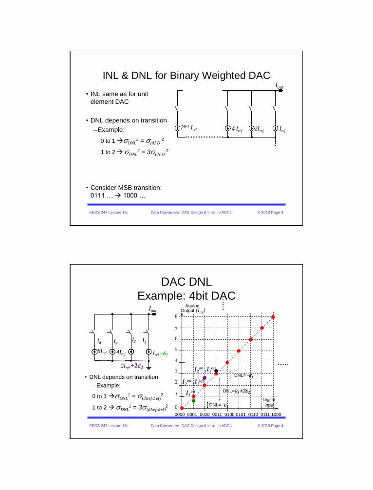
DAC DNL
Example: 4bit DAC
0000 0001 0010 0011 0100 0101 0110 0111 1000
Digital
Input
Analog Output [Iref]
8
7
6
5
4
3
2
1
0
4Iref Iref –e1
Iout
8Iref
I8 I4I2 I1
I2on ,I1
on
I2on ,I1
off
I1on
• DNL depends on transition
– Example:
0 to 1sDNL2 = s(dIref/Iref)
2
1 to 2 sDNL2 = 3s(dIref/Iref)
2
.....
.....
2Iref +2e2
DNL= -e1
DNL=e1+2e2
DNL= -e1
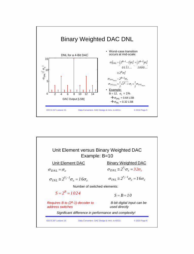
EECS 247 Lecture 15: Data Converters- DAC Design & Intro. to ADCs © 2010 Page 5
Binary Weighted DAC DNL
) )
DNLmax
BINL DNLmax max
2 B 1 2 B 1 2DNL
B 2
B / 2
1 12 1
2 2
2 1 2
0111... 1000...
2
2
e
e e
e
e
s s s
s
s s
s s s
+
• Worst-case transition occurs at mid-scale:
• Example:
B = 12, se = 1%
sDNL = 0.64 LSB
sINL = 0.32 LSB
2 4 6 8 10 12 140
5
10
15
DAC Output [LSB]
sD
NL
2/
se2
DNL for a 4-Bit DAC
EECS 247 Lecture 15: Data Converters- DAC Design & Intro. to ADCs © 2010 Page 6
Unit Element versus Binary Weighted DAC
Example: B=10
B2
DNL
1
B
INL 2 1
S 2 1 24
6
0
e
e e
s s
s s s
Significant difference in performance and complexity!
B2
B2
DNL
1INL
2 3
2 16
S B 10
2e
e e
es s
s s
s
s
Unit Element DAC Binary Weighted DAC
Number of switched elements:
Requires B to (2B-1) decoder to
address switches
B-bit digital input can be
used directly
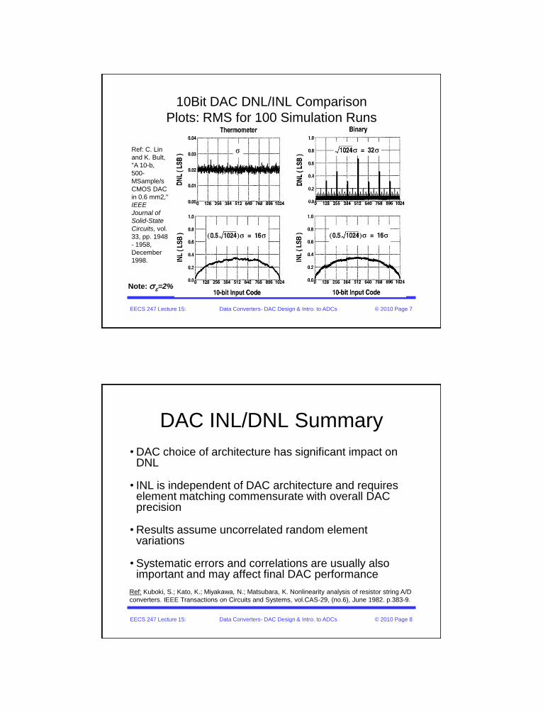
EECS 247 Lecture 15: Data Converters- DAC Design & Intro. to ADCs © 2010 Page 7
10Bit DAC DNL/INL Comparison
Plots: RMS for 100 Simulation Runs
Ref: C. Lin
and K. Bult,
"A 10-b,
500-
MSample/s
CMOS DAC
in 0.6 mm2,"
IEEE
Journal of
Solid-State
Circuits, vol.
33, pp. 1948
- 1958,
December
1998.
Note: se=2%
EECS 247 Lecture 15: Data Converters- DAC Design & Intro. to ADCs © 2010 Page 8
DAC INL/DNL Summary
• DAC choice of architecture has significant impact on DNL
• INL is independent of DAC architecture and requires element matching commensurate with overall DAC precision
• Results assume uncorrelated random element variations
• Systematic errors and correlations are usually also important and may affect final DAC performance
Ref: Kuboki, S.; Kato, K.; Miyakawa, N.; Matsubara, K. Nonlinearity analysis of resistor string A/D
converters. IEEE Transactions on Circuits and Systems, vol.CAS-29, (no.6), June 1982. p.383-9.
EECS 247 Lecture 15: Data Converters- DAC Design & Intro. to ADCs © 2010 Page 9
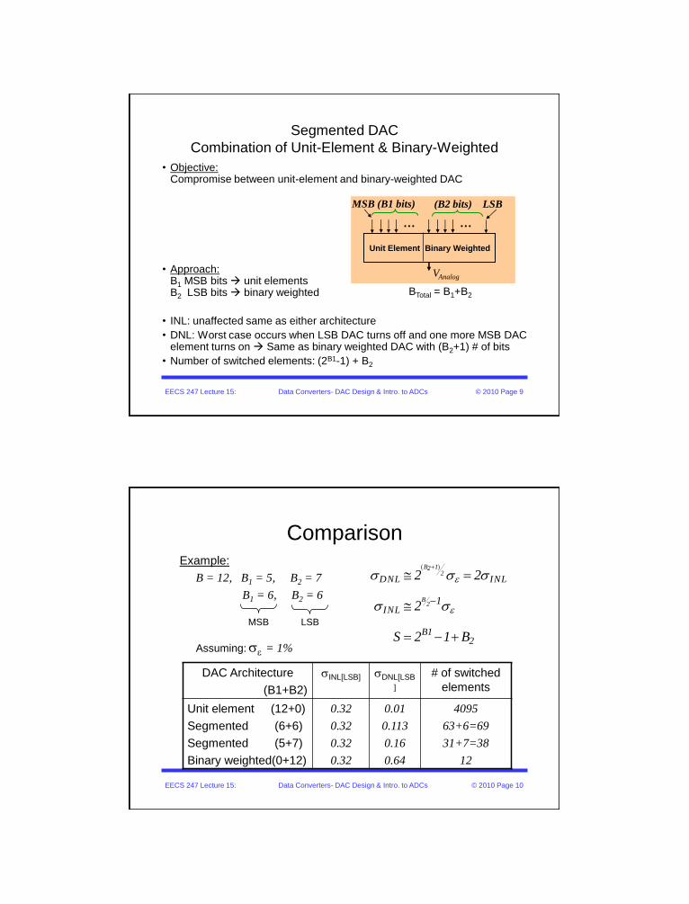
Segmented DAC
Combination of Unit-Element & Binary-Weighted
• Objective:Compromise between unit-element and binary-weighted DAC
• Approach:B1 MSB bits unit elementsB2 LSB bits binary weighted
• INL: unaffected same as either architecture
• DNL: Worst case occurs when LSB DAC turns off and one more MSB DAC element turns on Same as binary weighted DAC with (B2+1) # of bits
• Number of switched elements: (2B1-1) + B2
Unit Element Binary Weighted
VAnalog
MSB (B1 bits) (B2 bits) LSB
… …
BTotal = B1+B2
EECS 247 Lecture 15: Data Converters- DAC Design & Intro. to ADCs © 2010 Page 10
ComparisonExample:
B = 12, B1 = 5, B2 = 7
B1 = 6, B2 = 6
Assuming: se = 1%
)B 122
B2
DNL INL
INL
B12
1
2 2
2
S 2 1 B
e
e
s s s
s s
+
+
DAC Architecture
(B1+B2)
sINL[LSB] sDNL[LSB
]
# of switched
elements
Unit element (12+0)
Segmented (6+6)
Segmented (5+7)
Binary weighted(0+12)
0.32
0.32
0.32
0.32
0.01
0.113
0.16
0.64
4095
63+6=69
31+7=38
12
MSB LSB
EECS 247 Lecture 15: Data Converters- DAC Design & Intro. to ADCs © 2010 Page 11
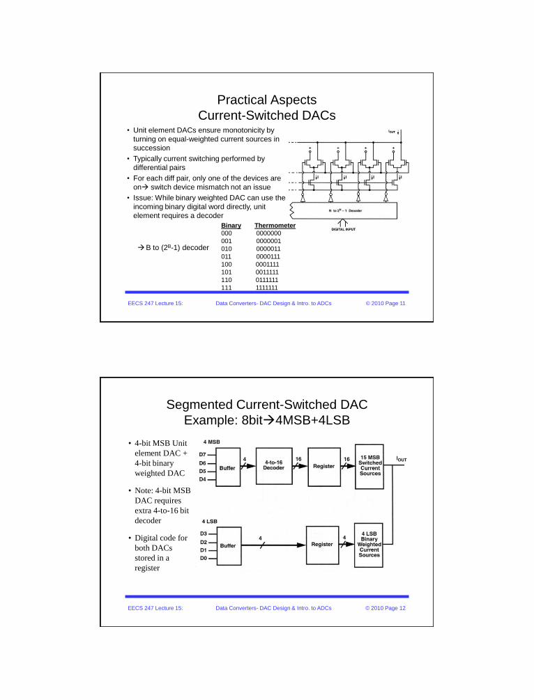
Practical Aspects
Current-Switched DACs
Binary Thermometer
000 0000000
001 0000001
010 0000011
011 0000111
100 0001111
101 0011111
110 0111111
111 1111111
• Unit element DACs ensure monotonicity by
turning on equal-weighted current sources in
succession
• Typically current switching performed by
differential pairs
• For each diff pair, only one of the devices are
on switch device mismatch not an issue
• Issue: While binary weighted DAC can use the
incoming binary digital word directly, unit
element requires a decoder
B to (2B-1) decoder
EECS 247 Lecture 15: Data Converters- DAC Design & Intro. to ADCs © 2010 Page 12
Segmented Current-Switched DAC
Example: 8bit4MSB+4LSB
• 4-bit MSB Unit
element DAC +
4-bit binary
weighted DAC
• Note: 4-bit MSB
DAC requires
extra 4-to-16 bit
decoder
• Digital code for
both DACs
stored in a
register

EECS 247 Lecture 15: Data Converters- DAC Design & Intro. to ADCs © 2010 Page 13
Segmented Current-Switched DAC
Cont’d
• 4-bit MSB Unit
element DAC + 4-
bit binary weighted
DAC
• Note: 4-bit MSB
DAC requires extra
4-to-16 bit decoder
• Digital code for
both DACs stored
in a register
EECS 247 Lecture 15: Data Converters- DAC Design & Intro. to ADCs © 2010 Page 14
Segmented Current-Switched DAC
Cont’d
• MSB Decoder
Domino logic
Example: D4,5,6,7=1 OUT=1
• Register
Latched NAND gate:
CTRL=1 OUT=INBRegister
Domino Logic
IN
EECS 247 Lecture 15: Data Converters- DAC Design & Intro. to ADCs © 2010 Page 15
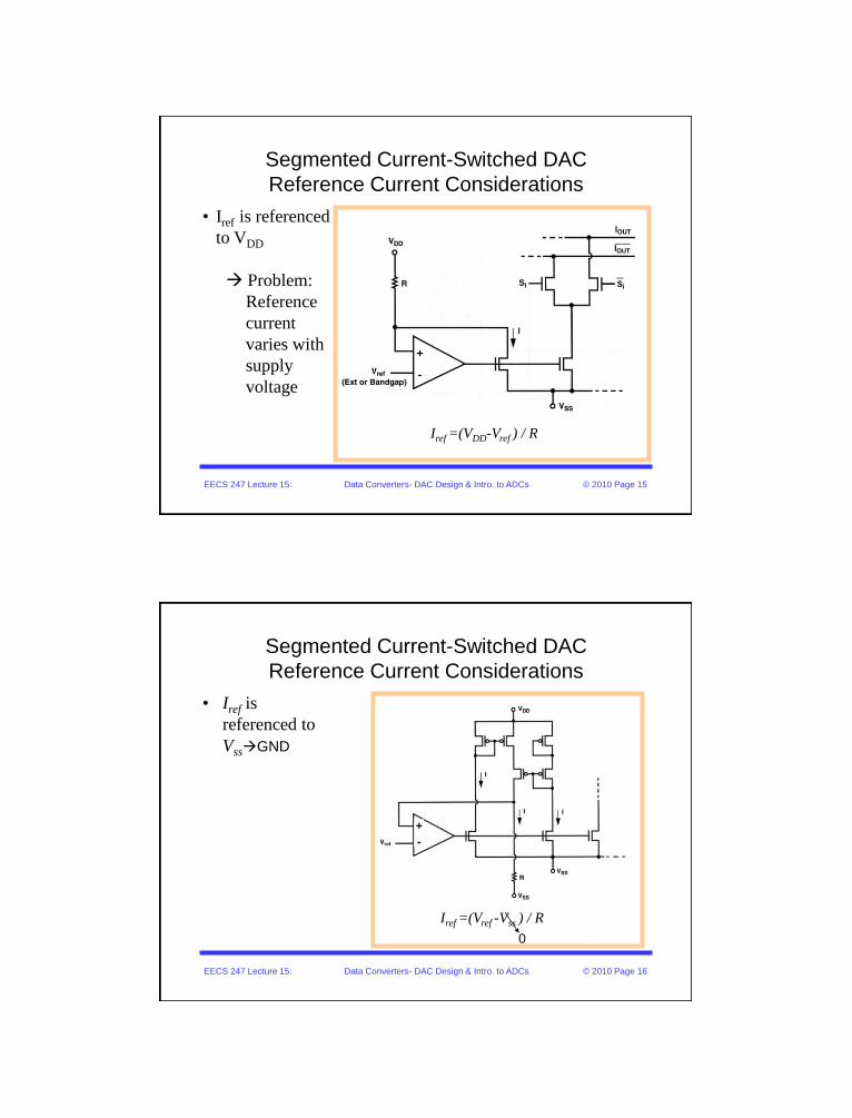
Segmented Current-Switched DAC
Reference Current Considerations
• Iref is referenced
to VDD
Problem:
Reference
current
varies with
supply
voltage
+
-
Iref =(VDD-Vref ) / R
EECS 247 Lecture 15: Data Converters- DAC Design & Intro. to ADCs © 2010 Page 16
Segmented Current-Switched DAC
Reference Current Considerations
• Iref is
referenced to
VssGND
+
-
Iref =(Vref -Vss ) / R
0
EECS 247 Lecture 15: Data Converters- DAC Design & Intro. to ADCs © 2010 Page 17
DAC Dynamic Non-Idealities
• Finite settling time– Linear settling issues: (e.g. RC time constants)
– Slew limited settling
• Spurious signal coupling– Coupling of clock/control signals to the output via
switches & switch charge injection
• Timing error related glitches– Control signal timing skew
EECS 247 Lecture 15: Data Converters- DAC Design & Intro. to ADCs © 2010 Page 18
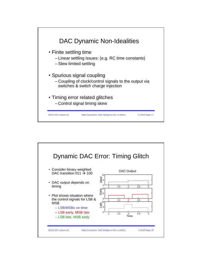
Dynamic DAC Error: Timing Glitch
• Consider binary weighted DAC transition 011 100
• DAC output depends on timing
• Plot shows situation where the control signals for LSB & MSB
– LSB/MSBs on time
– LSB early, MSB late
– LSB late, MSB early
1 1.5 2 2.5 30
5
10
Ideal
1 1.5 2 2.5 30
5
10
Ea
rly
1 1.5 2 2.5 30
5
10
Time
Late
DAC Output

EECS 247 Lecture 15: Data Converters- DAC Design & Intro. to ADCs © 2010 Page 19
Glitch Energy
• Glitch energy (worst case) proportional to: dt x 2B-1
• dt error in timing & 2B-1 associated with half of the switches changing
state
• LSB energy proportional to: T=1/fs
• Need dt x 2B-1 << T or dt << 2-B+1 T
• Examples:
Timing accuracy for logic circuitry associated with data converters much
more critical compared to digital circuitry e.g. DSP
fs [MHz] B dt [ps]
1
20
1000
12
16
12
<< 488
<< 1.5
<< 0.5
EECS 247 Lecture 15: Data Converters- DAC Design & Intro. to ADCs © 2010 Page 20
DAC Dynamic Errors
• To suppress effect of non-idealities:
– Retiming of current source control signals• Each current source has its own clocked latch
incorporated in the current cell
• Minimization of latch clock skew by careful layout ensuring simultaneous change of bits
– To minimize control and clock feed through to the output via G-D & G-S of the switches• Use of low-swing digital circuitry
EECS 247 Lecture 15: Data Converters- DAC Design & Intro. to ADCs © 2010 Page 21
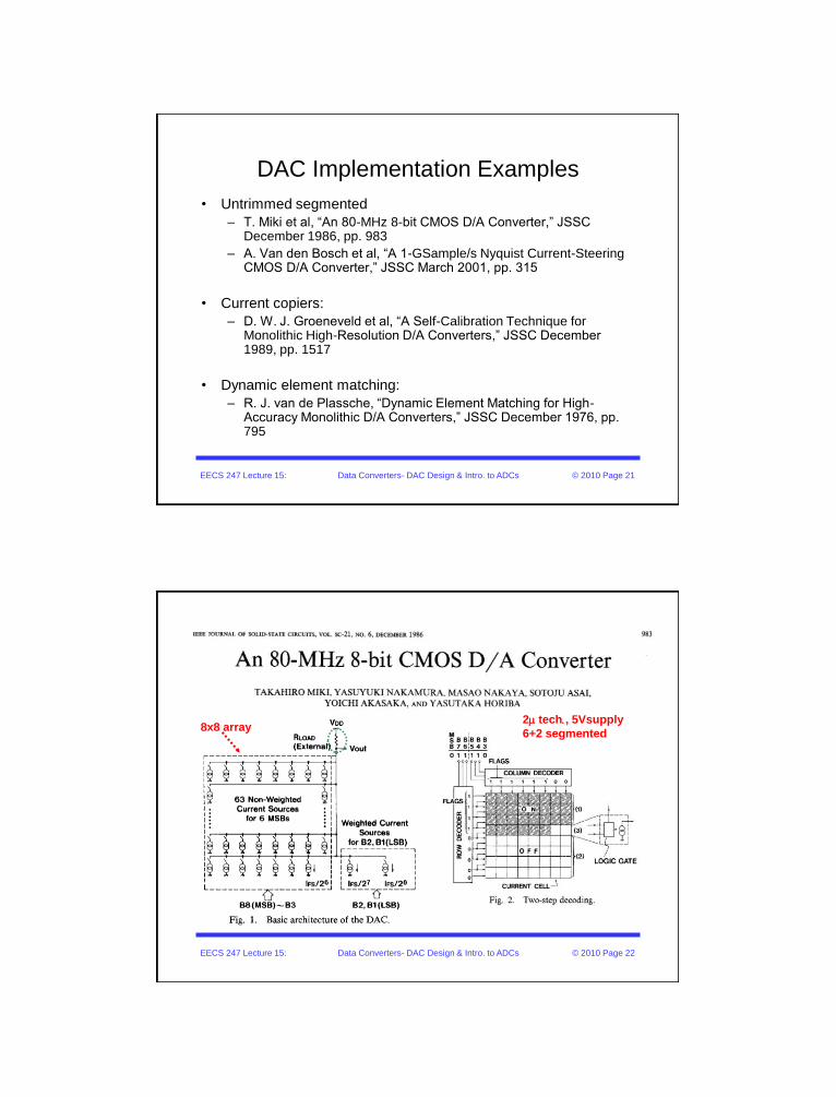
DAC Implementation Examples
• Untrimmed segmented
– T. Miki et al, “An 80-MHz 8-bit CMOS D/A Converter,” JSSC December 1986, pp. 983
– A. Van den Bosch et al, “A 1-GSample/s Nyquist Current-Steering CMOS D/A Converter,” JSSC March 2001, pp. 315
• Current copiers:
– D. W. J. Groeneveld et al, “A Self-Calibration Technique for Monolithic High-Resolution D/A Converters,” JSSC December 1989, pp. 1517
• Dynamic element matching:
– R. J. van de Plassche, “Dynamic Element Matching for High-Accuracy Monolithic D/A Converters,” JSSC December 1976, pp. 795
EECS 247 Lecture 15: Data Converters- DAC Design & Intro. to ADCs © 2010 Page 22
2m tech., 5Vsupply
6+2 segmented8x8 array
EECS 247 Lecture 15: Data Converters- DAC Design & Intro. to ADCs © 2010 Page 23
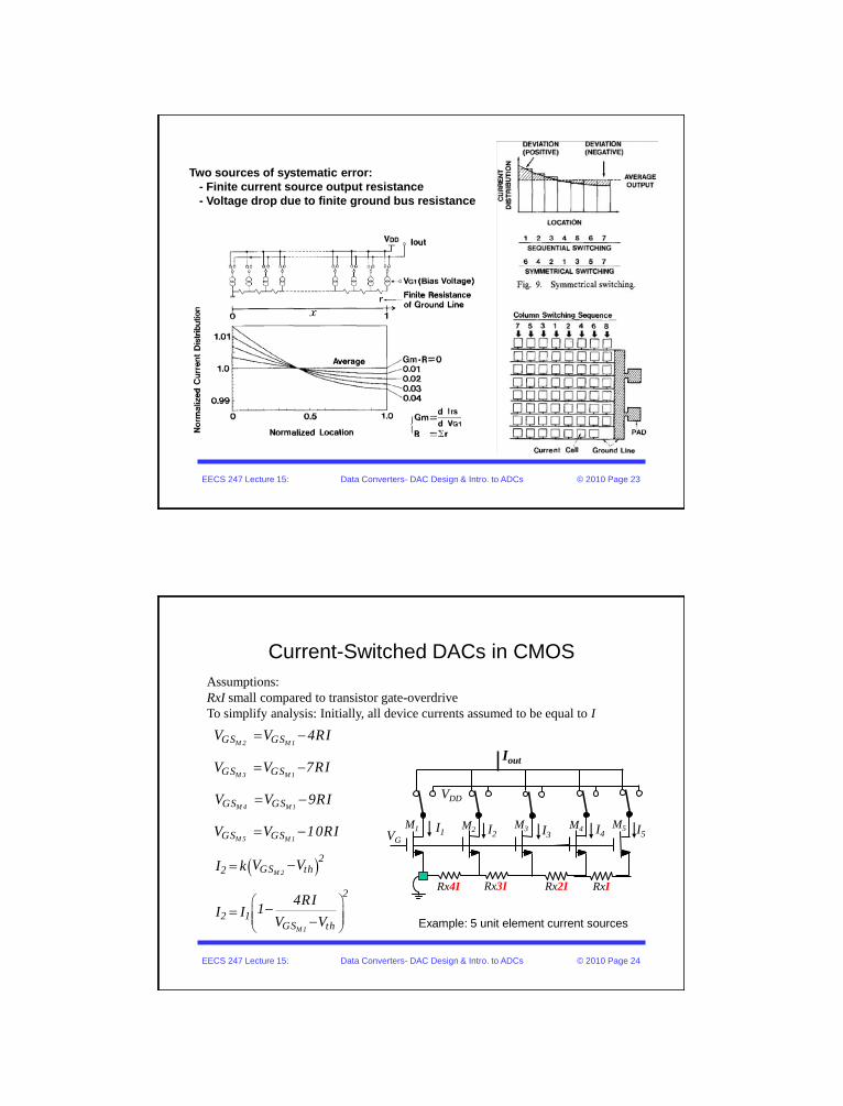
Two sources of systematic error:
- Finite current source output resistance
- Voltage drop due to finite ground bus resistance
EECS 247 Lecture 15: Data Converters- DAC Design & Intro. to ADCs © 2010 Page 24
Current-Switched DACs in CMOS
Iout
Example: 5 unit element current sources
VDD
I1 I2 I3 I4
Rx4I Rx3I Rx2I
M1 M2M3 M4 I5
M5
RxI
Assumptions:
RxI small compared to transistor gate-overdrive
To simplify analysis: Initially, all device currents assumed to be equal to I
)
M 2 M 1
M 3 M 1
M 4 M 1
M 5 M 1
M 2
M 1
GS GS
GS GS
GS GS
GS GS
2GS th2
2
2 1GS th
V V 4RI
V V 7RI
V V 9RI
V V 10RI
V VI k
4RI1I I
V V
VG

EECS 247 Lecture 15: Data Converters- DAC Design & Intro. to ADCs © 2010 Page 25
Current-Switched DACs in CMOS
Iout
Desirable to have gm small
Example: 5 unit element current sources
VDD
I1 I2 I3 I4
Rx4I Rx3I Rx2I
M1 M2M3 M4 I5
M5
RxI
)
)
)
)
)
M 2
M 1
M 1
M 1
M 1
M 1
M 1
M 1
M 1
M 1
M 1
M 1
2
2GS th2 1
GS th
1m
GS th2
m2 1 1 m
2
m3 1 1 m
2
m4 1 1 m
2
m5 1 1 m
4RI1V VI k I
V V
2Ig
V V
4RgI I I 1 4Rg1
2
7RgI I I 1 7Rg1
2
9RgI I I 1 9Rg1
2
10RgI I I 1 10Rg1
2
EECS 247 Lecture 15: Data Converters- DAC Design & Intro. to ADCs © 2010 Page 26
Two sources of systematic error:
- Finite current source output resistance
- Voltage drop due to finite ground bus resistance
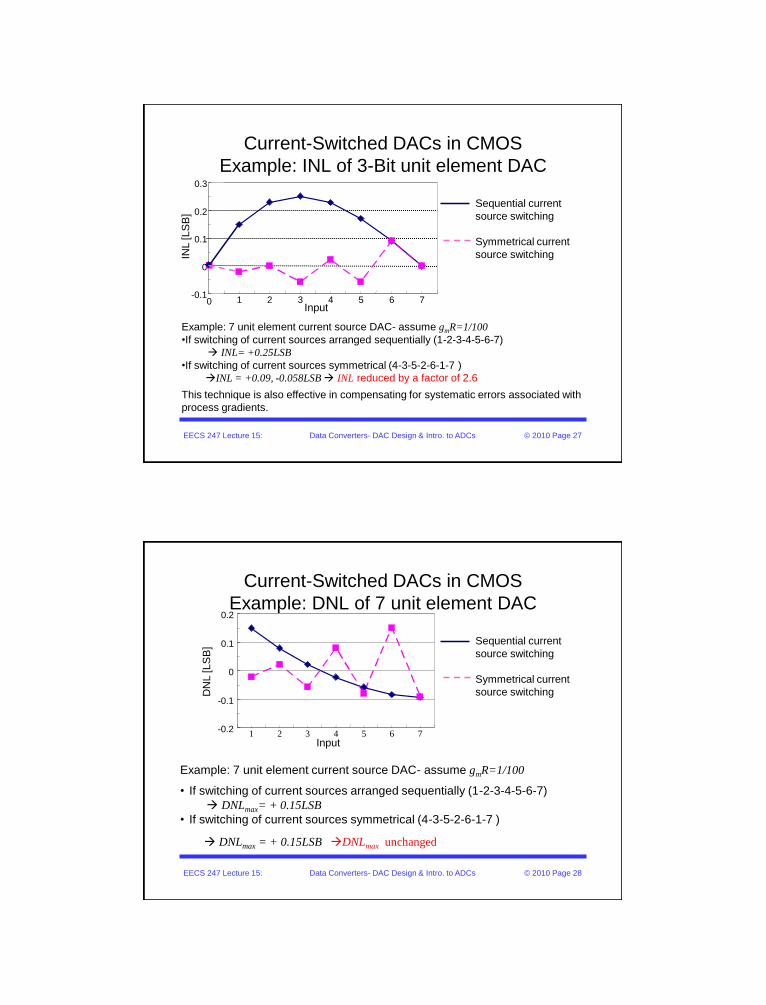
EECS 247 Lecture 15: Data Converters- DAC Design & Intro. to ADCs © 2010 Page 27
Current-Switched DACs in CMOS
Example: INL of 3-Bit unit element DAC
Input
INL [LS
B]
Example: 7 unit element current source DAC- assume gmR=1/100
•If switching of current sources arranged sequentially (1-2-3-4-5-6-7)
INL= +0.25LSB
•If switching of current sources symmetrical (4-3-5-2-6-1-7 )
INL = +0.09, -0.058LSB INL reduced by a factor of 2.6
This technique is also effective in compensating for systematic errors associated with
process gradients.
-0.1
0
0.1
0.2
0.3
1 2 3 4 5 6 70
Sequential current
source switching
Symmetrical current
source switching
EECS 247 Lecture 15: Data Converters- DAC Design & Intro. to ADCs © 2010 Page 28
Current-Switched DACs in CMOS
Example: DNL of 7 unit element DAC
Input
DN
L [LS
B]
Example: 7 unit element current source DAC- assume gmR=1/100
• If switching of current sources arranged sequentially (1-2-3-4-5-6-7)
DNLmax= + 0.15LSB
• If switching of current sources symmetrical (4-3-5-2-6-1-7 )
DNLmax = + 0.15LSB DNLmax unchanged
-0.2
-0.1
0
0.1
0.2
1 2 3 4 5 6 7
Sequential current
source switching
Symmetrical current
source switching
EECS 247 Lecture 15: Data Converters- DAC Design & Intro. to ADCs © 2010 Page 29
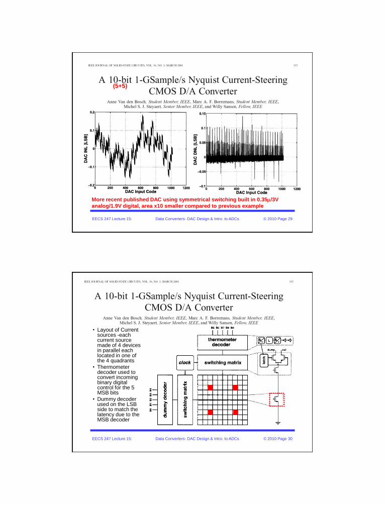
More recent published DAC using symmetrical switching built in 0.35m/3V
analog/1.9V digital, area x10 smaller compared to previous example
(5+5)
EECS 247 Lecture 15: Data Converters- DAC Design & Intro. to ADCs © 2010 Page 30
• Layout of Current sources -each current source made of 4 devices in parallel each located in one of the 4 quadrants
• Thermometer decoder used to convert incoming binary digital control for the 5 MSB bits
• Dummy decoder used on the LSB side to match the latency due to the MSB decoder
EECS 247 Lecture 15: Data Converters- DAC Design & Intro. to ADCs © 2010 Page 31
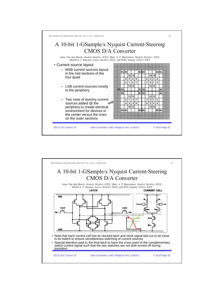
• Current source layout
– MSB current sources layout in the mid sections of the four quad
– LSB current sources mostly in the periphery
– Two rows of dummy current sources added @ the periphery to create identical environment for devices in the center versus the ones on the outer sections
EECS 247 Lecture 15: Data Converters- DAC Design & Intro. to ADCs © 2010 Page 32
• Note that each current cell has its clocked latch and clock signal laid out to be close to its switch to ensure simultaneous switching of current sources
• Special attention paid to the final latch to have the cross point of the complementary switch control signal such that the two switches are not both turned off during transition
t

EECS 247 Lecture 15: Data Converters- DAC Design & Intro. to ADCs © 2010 Page 33
• Measured DNL/INL with current associated with the current cells as variable
DNL/INL [LSB]
IFull-Scale [mA]
EECS 247 Lecture 15: Data Converters- DAC Design & Intro. to ADCs © 2010 Page 34
Called:
Current Copier
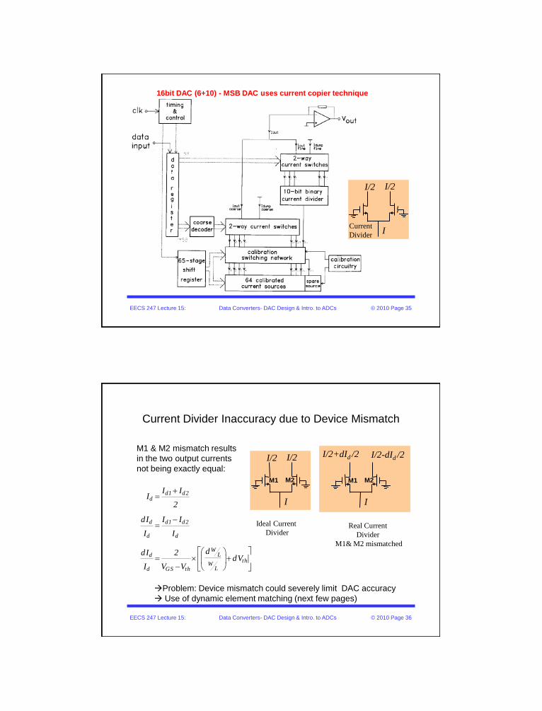
EECS 247 Lecture 15: Data Converters- DAC Design & Intro. to ADCs © 2010 Page 35
I
I/2 I/2
Current
Divider
16bit DAC (6+10) - MSB DAC uses current copier technique
EECS 247 Lecture 15: Data Converters- DAC Design & Intro. to ADCs © 2010 Page 36
I
I/2 I/2
Ideal Current
Divider
Current Divider Inaccuracy due to Device Mismatch
I
I/2+dId /2
Real Current
Divider
M1& M2 mismatched
I/2-dId /2
M1 M2M1 M2
Problem: Device mismatch could severely limit DAC accuracy
Use of dynamic element matching (next few pages)
M1 & M2 mismatch results
in the two output currents
not being exactly equal:
d1 d2d
d d1 d2
d d
WLd
thW
Ld GS th
I II
2
dI I I
I I
ddI 2dV
I V V
+
+
EECS 247 Lecture 15: Data Converters- DAC Design & Intro. to ADCs © 2010 Page 37
• Idea is:
o Even though the two
outputs of the diff pair
divider may not be
exactly equal (due to
device mismatch)
o The sum of the two
currents stays
constant
By using switching
tie both outputs to
sum of the two
EECS 247 Lecture 15: Data Converters- DAC Design & Intro. to ADCs © 2010 Page 38
Dynamic Element Matching
) )
(1) ( 2 )2 2
2
1 1o
o
I II
2
1 1I
2 2
I
2
+
+ +
)
)
(1) 1o 11 2
(1) 1o 12 2
I I 1
I I 1
+
/ 2 error 1
I1
During F1During F2
I2
fclk
Io
Io/2Io/2 )
)
( 2 ) 1o 11 2
( 2 ) 1o 12 2
I I 1
I I 1
+
Average of I2 :
Note: DAC frequency of operation < fclk
T=1/fclk

EECS 247 Lecture 15: Data Converters- DAC Design & Intro. to ADCs © 2010 Page 39
Dynamic Element Matching
) )
(1) ( 2 )2 2
2
1 1o
o
I II
2
1 1I
2 2
I
2
+
+ +
)
)
(1) 1o 11 2
(1) 1o 12 2
I I 1
I I 1
+
During F1During F2
)
)
( 2 ) 1o 11 2
( 2 ) 1o 12 2
I I 1
I I 1
+
Average of I2 :
Note: DAC frequency of operation < fclk
T=1/fclk
I1I2
fclk
Io/2+1 Io/2- 1
Io
EECS 247 Lecture 15: Data Converters- DAC Design & Intro. to ADCs © 2010 Page 40
Note:
For optimum current division accuracy clock
frequency is divided by two for each finer division
Problem: DAC frequency of operation drastically
reduced
Note: What if the same
clock frequency is used?
EECS 247 Lecture 15: Data Converters- DAC Design & Intro. to ADCs © 2010 Page 41
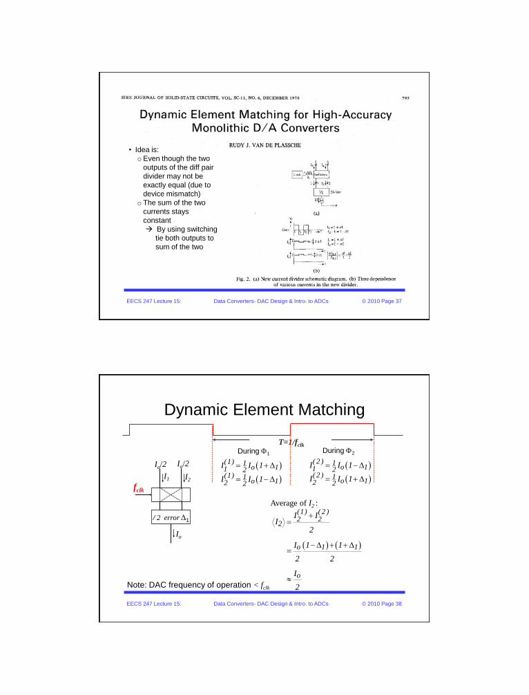
Dynamic Element Matching
)
)
)
) )2141
2
)1(
121)1(
3
121)1(
2
121)1(
1
11
1
1
1
++
+
+
o
o
o
I
II
II
II )
)
)
) )2141
2
)2(
121)2(
3
121)2(
2
121)2(
1
11
1
1
1
+
o
o
o
I
II
II
II
During F1During F2
) ) ) )
)21
2121
)2(
3
)1(
33
14
2
1111
4
2
+
+++
+
o
o
I
I
III
E.g. 1 = 2 = 1% matching error is (1%)2 = 0.01%
/ 2 error 1
I1
I2
fclk
Io
Io/2
/ 2 error 2
I3 I4
fclk
Io/4Io/4
EECS 247 Lecture 15: Data Converters- DAC Design & Intro. to ADCs © 2010 Page 42
• Bipolar 12-bit DAC using dynamic element matching built in 1976
• Element matching clock frequency 100kHz
• INL <0.25LSB!

EECS 247 Lecture 15: Data Converters- DAC Design & Intro. to ADCs © 2010 Page 43
Example: State-
of-the-Art current
steering DAC
Segmented:
6bit unit-element
8bit binary
EECS 247 Lecture 15: Data Converters- DAC Design & Intro. to ADCs © 2010 Page 44
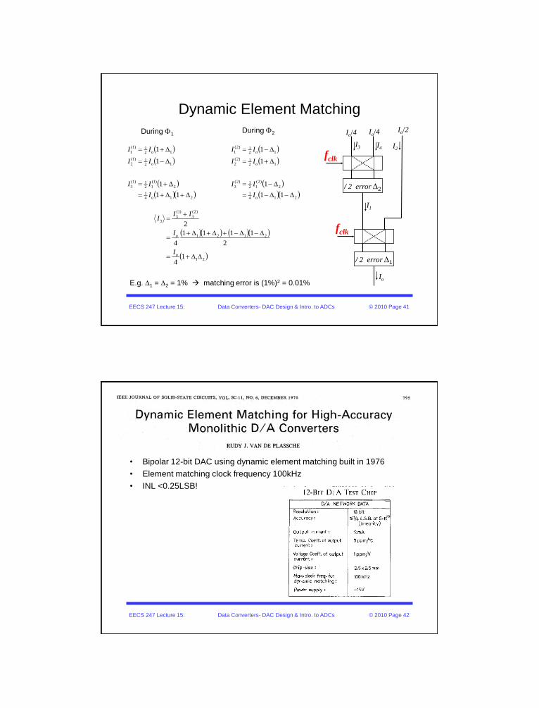
EECS 247 Lecture 15: Data Converters- DAC Design & Intro. to ADCs © 2010 Page 45
DAC In the Big Picture
• Learned to build DACs– Convert the
incoming digital signal to analog
• DAC output staircase form
• Some applications require filtering (smoothing) of DAC output
Reconstruction filter
Analog
Post processing
D/A
Conversion
DSP
A/D
Conversion
Analog
Preprocessing
Analog Input
Analog Output
000
...001...
110
Anti-Aliasing
Filter
Sampling
+Quantization
"Bits to
Staircase"
Reconstruction
Filter
EECS 247 Lecture 15: Data Converters- DAC Design & Intro. to ADCs © 2010 Page 46
DAC Reconstruction Filter
• Output of DAC:
– Frequency domain: DAC input
spectrum shaped by S/H sinc
function
– Time domain: Staircase shaped
waveform
• Tasks:
– Correct for sinc droop if needed
– Remove “aliases”
(stair-case approximation)
Reconstruction filter: Need and
requirements depend on
application
B fs/2
0 0.5 1 1.5 2 2.5 3
x 106
0
0.5
1
DA
C Input
0 0.5 1 1.5 2 2.5 3
x 106
0
0.5
1
sin
c
0 0.5 1 1.5 2 2.5 30
0.5
1
DA
C O
utp
ut
Normalized Frequency f/fs
EECS 247 Lecture 15: Data Converters- DAC Design & Intro. to ADCs © 2010 Page 47
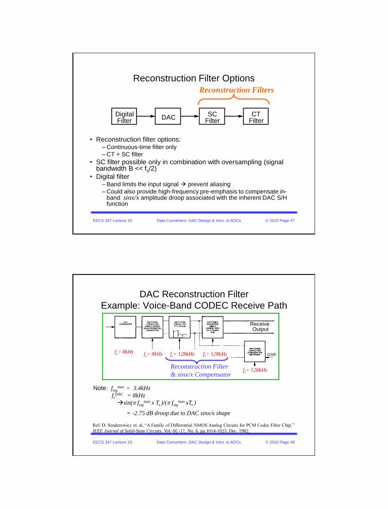
Reconstruction Filter Options
• Reconstruction filter options:– Continuous-time filter only
– CT + SC filter
• SC filter possible only in combination with oversampling (signal bandwidth B << fs/2)
• Digital filter– Band limits the input signal prevent aliasing
– Could also provide high-frequency pre-emphasis to compensate in-band sinx/x amplitude droop associated with the inherent DAC S/H function
DigitalFilter
DACSC
FilterCT
Filter
Reconstruction Filters
EECS 247 Lecture 15: Data Converters- DAC Design & Intro. to ADCs © 2010 Page 48
DAC Reconstruction Filter
Example: Voice-Band CODEC Receive Path
Ref: D. Senderowicz et. al, “A Family of Differential NMOS Analog Circuits for PCM Codec Filter Chip,”
IEEE Journal of Solid-State Circuits, Vol.-SC-17, No. 6, pp.1014-1023, Dec. 1982.
Note: fsigmax = 3.4kHz
fsDAC = 8kHz
sin(p fsigmax x Ts )/(p fsig
max xTs )
= -2.75 dB droop due to DAC sinx/x shape
Receive Output
fs= 8kHz fs= 128kHzfs= 8kHz fs= 128kHz
fs= 128kHz
GSR
Reconstruction Filter
& sinx/x Compensator
EECS 247 Lecture 15: Data Converters- DAC Design & Intro. to ADCs © 2010 Page 49
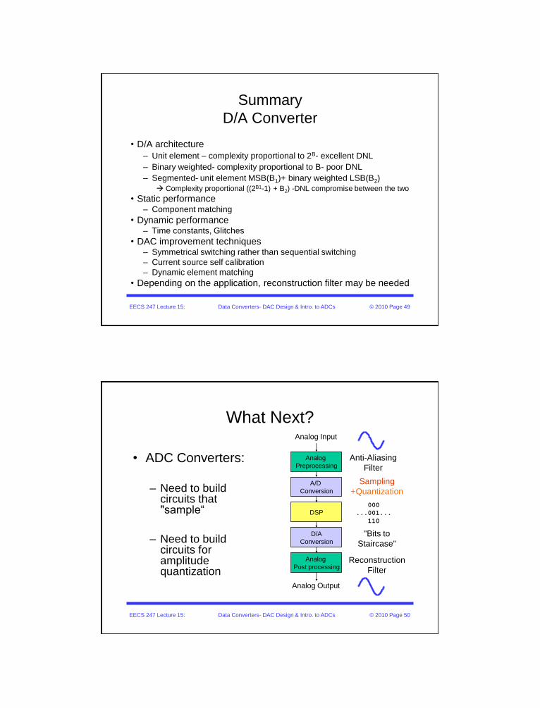
Summary
D/A Converter
• D/A architecture
– Unit element – complexity proportional to 2B- excellent DNL
– Binary weighted- complexity proportional to B- poor DNL
– Segmented- unit element MSB(B1)+ binary weighted LSB(B2)
Complexity proportional ((2B1-1) + B2) -DNL compromise between the two
• Static performance– Component matching
• Dynamic performance– Time constants, Glitches
• DAC improvement techniques – Symmetrical switching rather than sequential switching
– Current source self calibration
– Dynamic element matching
• Depending on the application, reconstruction filter may be needed
EECS 247 Lecture 15: Data Converters- DAC Design & Intro. to ADCs © 2010 Page 50
What Next?
• ADC Converters:
– Need to build circuits that "sample“
– Need to build circuits for amplitude quantization
Analog
Post processing
D/A
Conversion
DSP
A/D
Conversion
Analog
Preprocessing
Analog Input
Analog Output
000
...001...
110
Anti-Aliasing
Filter
Sampling
+Quantization
"Bits to
Staircase"
Reconstruction
Filter

EECS 247 Lecture 15: Data Converters- DAC Design & Intro. to ADCs © 2010 Page 51
Analog-to-Digital Converters
•Two categories:
– Nyquist rate ADCs fsigmax ~ 0.5xfsampling
• Maximum achievable signal bandwidth higher compared
to oversampled type
• Resolution limited to max. 14bits
– Oversampled ADCs fsigmax << 0.5xfsampling
• Maximum achievable signal bandwidth significantly lower
compared to nyquist
• Maximum achievable resolution high (18 to 20bits!)
EECS 247 Lecture 15: Data Converters- DAC Design & Intro. to ADCs © 2010 Page 52
MOS Sampling Circuits
EECS 247 Lecture 15: Data Converters- DAC Design & Intro. to ADCs © 2010 Page 53
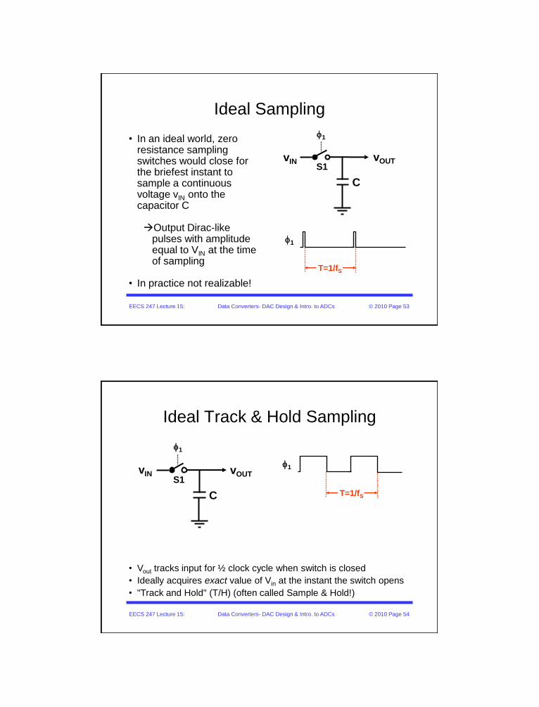
Ideal Sampling
• In an ideal world, zero resistance sampling switches would close for the briefest instant to sample a continuous voltage vIN onto the capacitor C
Output Dirac-like pulses with amplitude equal to VIN at the time of sampling
• In practice not realizable!
vIN vOUT
C
S1
1
1
T=1/fS
EECS 247 Lecture 15: Data Converters- DAC Design & Intro. to ADCs © 2010 Page 54
Ideal Track & Hold Sampling
vIN vOUT
C
S1
1
• Vout tracks input for ½ clock cycle when switch is closed
• Ideally acquires exact value of Vin at the instant the switch opens
• "Track and Hold" (T/H) (often called Sample & Hold!)
1
T=1/fS

EECS 247 Lecture 15: Data Converters- DAC Design & Intro. to ADCs © 2010 Page 55
Ideal T/H Sampling
Continuous
Time
T/H signal
(Sampled-Data
Signal)
Clock
Discrete-Time
Signal
time
Tra
ck
Ho
ld
EECS 247 Lecture 15: Data Converters- DAC Design & Intro. to ADCs © 2010 Page 56
Practical Sampling
Issues
vIN vOUT
C
M1
1
• Switch induced noise due to M1 finite channel resistance
• Clock jitter
• Finite Rsw limited bandwidth finite acquisition time
• Rsw = f(Vin) distortion
• Switch charge injection & clock feedthrough

EECS 247 Lecture 15: Data Converters- DAC Design & Intro. to ADCs © 2010 Page 57
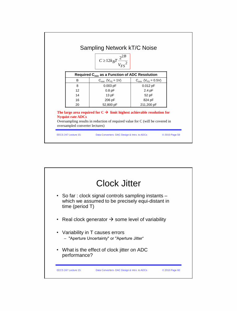
Sampling Circuit kT/C Noise
• Switch resistance & sampling capacitor form a low-pass filter
• Noise associated with the switch resistance results in Total noise
variance= kT/C @ the output (see noise analysis in Lecture 1)
• In high resolution ADCs kT/C noise at times dominates overall
minimum signal handling capability (power dissipation
considerations).
vINvOUT
C
S1RvIN vOUT
C
M1
1 4kTRf
EECS 247 Lecture 15: Data Converters- DAC Design & Intro. to ADCs © 2010 Page 58
Sampling Network kT/C Noise
For ADCs sampling capacitor size is usually chosen based on having thermal
noise smaller or equal or at times larger compared to quantization noise:
Assumption: Nyquist rate ADC
2
2
2
2
2
212
1212
12
noise Q than equal)(or less is level noise thermalsuch that C Choose
12 power noiseon quantizati Total :ADC rateNyquist aFor
FS
B
B
FS
B
B
B
VTkC
VTkC
C
Tk
EECS 247 Lecture 15: Data Converters- DAC Design & Intro. to ADCs © 2010 Page 59
Sampling Network kT/C Noise
Required Cmin as a Function of ADC Resolution
B Cmin (VFS = 1V) Cmin (VFS = 0.5V)
8
12
14
16
20
0.003 pF
0.8 pF
13 pF
206 pF
52,800 pF
0.012 pF
2.4 pF
52 pF
824 pF
211,200 pF
2
2212
FS
B
BV
TkC
The large area required for C limit highest achievable resolution for
Nyquist rate ADCs
Oversampling results in reduction of required value for C (will be covered in
oversampled converter lectures)
EECS 247 Lecture 15: Data Converters- DAC Design & Intro. to ADCs © 2010 Page 60
Clock Jitter
• So far : clock signal controls sampling instants –which we assumed to be precisely equi-distant in time (period T)
• Real clock generator some level of variability
• Variability in T causes errors– "Aperture Uncertainty" or "Aperture Jitter“
• What is the effect of clock jitter on ADC performance?
EECS 247 Lecture 15: Data Converters- DAC Design & Intro. to ADCs © 2010 Page 61
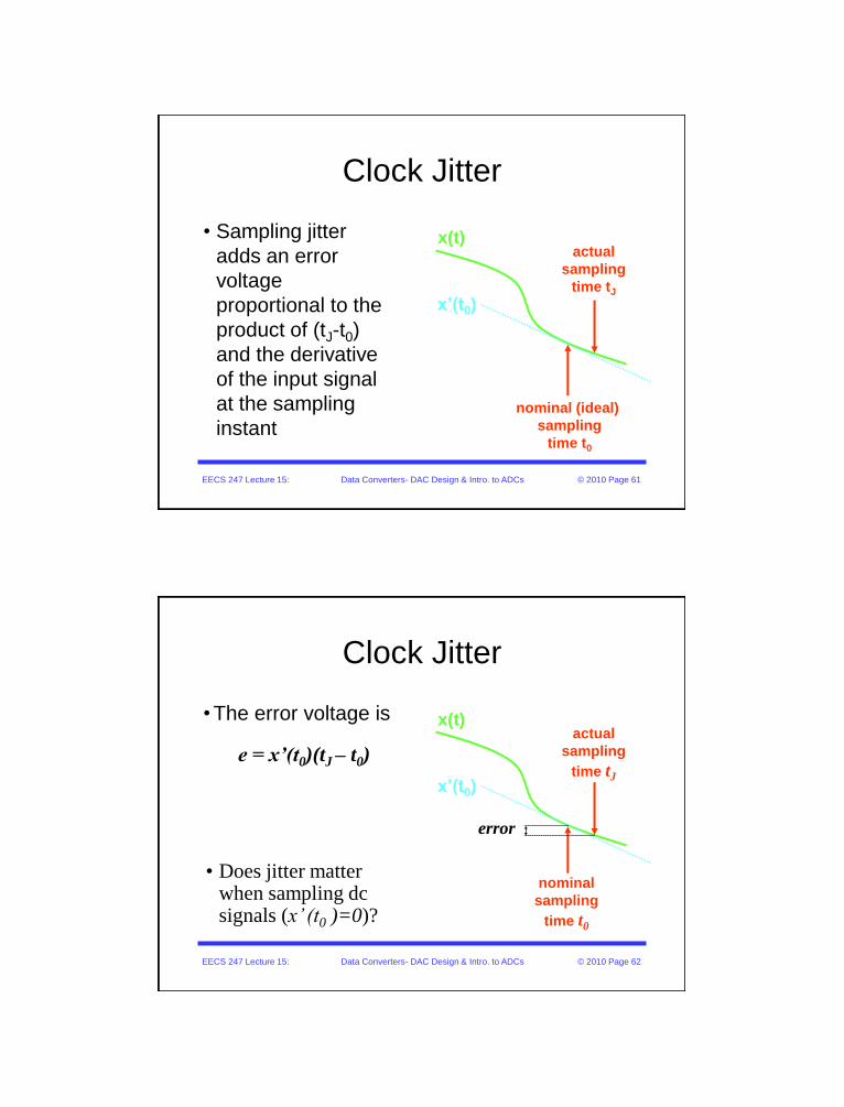
Clock Jitter
• Sampling jitter
adds an error
voltage
proportional to the
product of (tJ-t0)
and the derivative
of the input signal
at the sampling
instantnominal (ideal)
sampling
time t0
actual
sampling
time tJ
x(t)
x’(t0)
EECS 247 Lecture 15: Data Converters- DAC Design & Intro. to ADCs © 2010 Page 62
Clock Jitter
• The error voltage is
nominal
sampling
time t0
actual
sampling
time tJ
x(t)
x’(t0)
e = x’(t0)(tJ – t0)
error
• Does jitter matter when sampling dc signals (x’ (t0 )=0)?
EECS 247 Lecture 15: Data Converters- DAC Design & Intro. to ADCs © 2010 Page 63
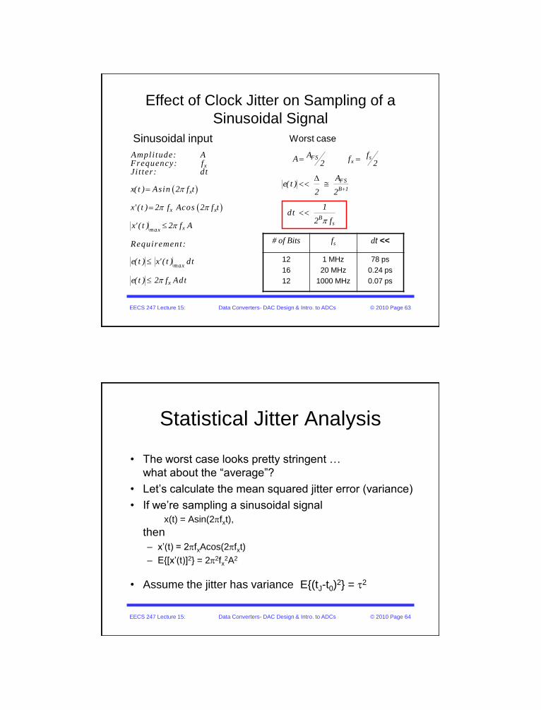
Effect of Clock Jitter on Sampling of a
Sinusoidal Signal
Sinusoidal input Worst case
# of Bits fs dt <<
12
16
12
1 MHz
20 MHz
1000 MHz
78 ps
0.24 ps
0.07 ps
sFSx
FS
B 1
Bs
fAA f
2 2
Ae( t )
2 2
1dt
2 fp
+
)
)
x
x
x x
xmax
max
x
Ampli tude: AFrequency: f Ji t ter: dt
x( t ) Asin 2 f t
x' ( t ) 2 f Acos 2 f t
x' ( t ) 2 f A
Requirement:
e( t ) x' ( t ) dt
e( t ) 2 f Adt
p
p p
p
p
EECS 247 Lecture 15: Data Converters- DAC Design & Intro. to ADCs © 2010 Page 64
Statistical Jitter Analysis
• The worst case looks pretty stringent …
what about the “average”?
• Let’s calculate the mean squared jitter error (variance)
• If we’re sampling a sinusoidal signal
x(t) = Asin(2pfxt),
then
– x’(t) = 2pfxAcos(2pfxt)
– E{[x’(t)]2} = 2p2fx2A2
• Assume the jitter has variance E{(tJ-t0)2} = 2
EECS 247 Lecture 15: Data Converters- DAC Design & Intro. to ADCs © 2010 Page 65
Statistical Jitter Analysis
• If x’(t) and the jitter are independent
– E{[x’(t)(tJ-t0)]2}= E{[x’(t)]2} E{(tJ-t0)
2}
• Hence, the jitter error power is
• If the jitter is uncorrelated from sample to sample, this “jitter noise” is white
E{e2} = 2p2fx2A22
EECS 247 Lecture 15: Data Converters- DAC Design & Intro. to ADCs © 2010 Page 66
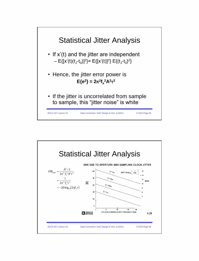
Statistical Jitter Analysis
)p
p
p
x
x
x
f
f
Af
ADR
2log20
2
1
2
2/
10
222
2222
2
jitter
EECS 247 Lecture 15: Data Converters- DAC Design & Intro. to ADCs © 2010 Page 67
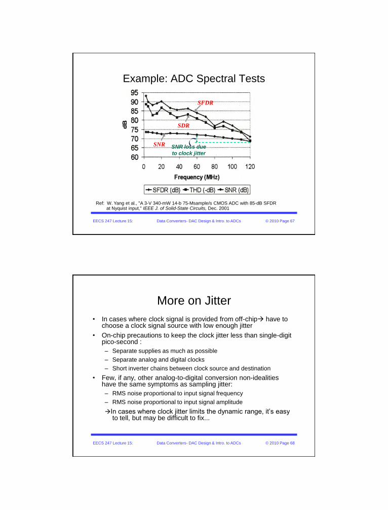
Example: ADC Spectral Tests
SFDR
SDR
SNR
Ref: W. Yang et al., "A 3-V 340-mW 14-b 75-Msample/s CMOS ADC with 85-dB SFDR at Nyquist input," IEEE J. of Solid-State Circuits, Dec. 2001
SNR loss due
to clock jitter
EECS 247 Lecture 15: Data Converters- DAC Design & Intro. to ADCs © 2010 Page 68
More on Jitter
• In cases where clock signal is provided from off-chip have to choose a clock signal source with low enough jitter
• On-chip precautions to keep the clock jitter less than single-digit pico-second :
– Separate supplies as much as possible
– Separate analog and digital clocks
– Short inverter chains between clock source and destination
• Few, if any, other analog-to-digital conversion non-idealities have the same symptoms as sampling jitter:
– RMS noise proportional to input signal frequency
– RMS noise proportional to input signal amplitude
In cases where clock jitter limits the dynamic range, it’s easy to tell, but may be difficult to fix...