Embed Size (px)
Citation preview
Ingram School of Engineering Digital Logic Texas State University
EE2420 Digital Logic
Laboratory Assignment
”Adder Design using Verilog HDL
Name:
Date Performed:
Partners:
Instructors: Dr. LarsonDr. Aslan
1
Ingram School of Engineering Digital Logic Texas State University
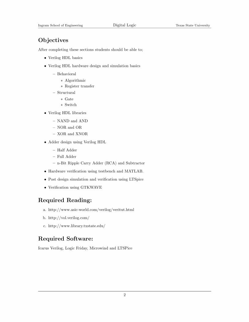
Objectives
After completing these sections students should be able to;
• Verilog HDL basics
• Verilog HDL hardware design and simulation basics
– Behavioral
∗ Algorithmic
∗ Register transfer
– Structural
∗ Gate
∗ Switch
• Verilog HDL libraries
– NAND and AND
– NOR and OR
– XOR and XNOR
• Adder design using Verilog HDL
– Half Adder
– Full Adder
– n-Bit Ripple Carry Adder (RCA) and Subtractor
• Hardware verification using testbench and MATLAB.
• Post design simulation and verification using LTSpice
• Verification using GTKWAVE
Required Reading:
a. http://www.asic-world.com/verilog/veritut.html
b. http://vol.verilog.com/
c. http://www.library.txstate.edu/
Required Software:
Icarus Verilog, Logic Friday, Microwind and LTSPice
2
Ingram School of Engineering Digital Logic Texas State University
Information [1]
Introduction to Verilog HDL [2]
Schematic Modeling
Digital
Simulation
Verilog
Extraction
SPICE
Extraction
DSCH
LTSpice
Verilog File
Verilog HDL(Design)
Verilog HDL(Verification)
Simulation
Compile Icarus Verilog
Logic Friday
Modelsim
Verilog
Compiler
nanoLambdaLayout Editor
Constraints
Technology
Place & Route
AnalysisDRC, ERC
Delay Analyzer
Crosstalk Analyzer
2D Cross Section
3D Analyzer
Layout
Extraction
ProTHUMBAdvanced post layout
simulator
Layout
Conversion
Spice, CIF MicrowindLTSpice
Tape Out
(FAB)
Synthesis
Floorplanning
Constraints
Technology
Place & Route Analysis
Programming
File
.bit or .ied
FPGA
Xilinx
(ISE)
Altera
(Quartus)
I/O CardsController
Display
Key Pad
Video/Audio/Image
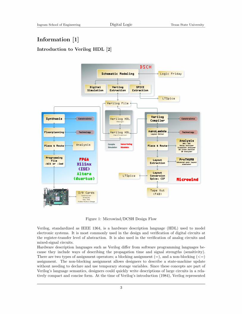
Figure 1: Microwind/DCSH Design Flow
Verilog, standardized as IEEE 1364, is a hardware description language (HDL) used to modelelectronic systems. It is most commonly used in the design and verification of digital circuits atthe register-transfer level of abstraction. It is also used in the verification of analog circuits andmixed-signal circuits.Hardware description languages such as Verilog differ from software programming languages be-cause they include ways of describing the propagation time and signal strengths (sensitivity).There are two types of assignment operators; a blocking assignment (=), and a non-blocking (<=)assignment. The non-blocking assignment allows designers to describe a state-machine updatewithout needing to declare and use temporary storage variables. Since these concepts are part ofVerilog’s language semantics, designers could quickly write descriptions of large circuits in a rela-tively compact and concise form. At the time of Verilog’s introduction (1984), Verilog represented
3
Ingram School of Engineering Digital Logic Texas State University
a tremendous productivity improvement for circuit designers who were already using graphicalschematic capture software and specially written software programs to document and simulateelectronic circuits.The designers of Verilog wanted a language with syntax similar to the C programming language,which was already widely used in engineering software development. Like C, Verilog is case-sensitive and has a basic preprocessor (though less sophisticated than that of ANSI C/C++. Itscontrol flow keywords (if/else, for, while, case, etc.) are equivalent, and its operator precedenceis compatible with C. Syntactic differences include: required bit-widths for variable declarations,demarcation of procedural blocks (Verilog uses begin/end instead of curly braces {}), and manyother minor differences. Verilog requires that variables be given a definite size. In C these sizesare assumed from the ’type’ of the variable (for instance an integer type may be 8 bits).
Structural Verilog Introduction
Throughout rest of this lab, you will design digital circuits using Verilog, a popular hardwaredescription language (HDL). You will learn structural Verilog (describe circuits in terms of wires,gates and modules) and verification using testbench.
Introduction to Verilog HDL [3]
Modules:
In Verilog, circuit components are designed inside a module. Modules can contain both structuraland behavioral statements. Structural statements represent circuit components like logic gates,counters, and microprocessors. Behavioral level statements are programming statements that haveno direct mapping to circuit components like loops, if-then statements, and stimulus vectors whichare used to exercise a circuit.
Create a Folder YourName Verilog in your U Drive
Exercise (1): - save your files as ”EE2420 E1.v” and ”EE2420 E1 tb.v”
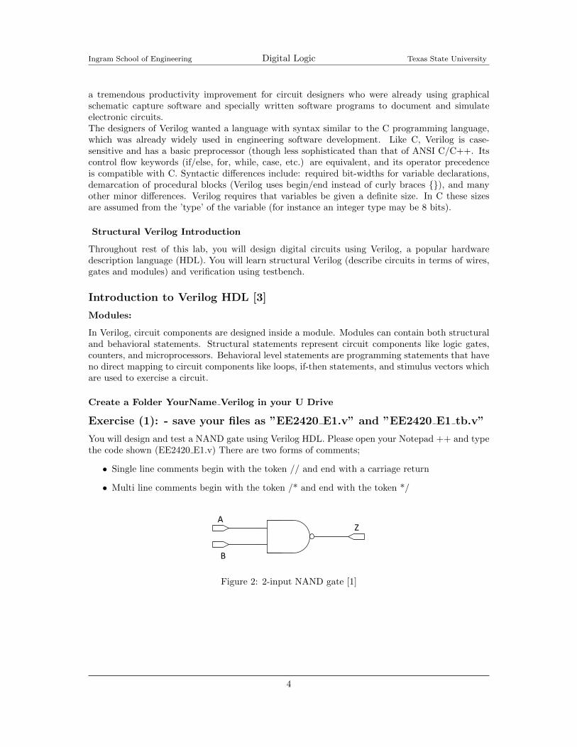
You will design and test a NAND gate using Verilog HDL. Please open your Notepad ++ and typethe code shown (EE2420 E1.v) There are two forms of comments;
• Single line comments begin with the token // and end with a carriage return
• Multi line comments begin with the token /* and end with the token */
A
B
Z
Figure 2: 2-input NAND gate [1]
4
Ingram School of Engineering Digital Logic Texas State University
/∗Name : Your NameF i l e : EE2420 E1 . vDesc r ip t i on : This i s a 2 input NAND Gate∗/
module EE2420_E1 ( z , a , b ) ; // de c l a r e module name and port l i s t
input a , b ; // de c l a r e port s i g n a l s − inputoutput z ; // de c l a r e port s i g n a l s − outputnand nand01 ( z , a , b ) ; // d e s c r i p t i o n o f NAND gate
endmodule
Before we start using this NAND gate we need to make sure it operates correctly. The verificationof the code will be done using a testbench file. Please open your Notepad ++ and type the codeshown (EE2420 E1 tb.v). More information please look at this tutorial [4].
/∗Name : Your NameF i l e : EE2420 E1 tb . vDesc r ip t i on : This i s a 2 input NAND Gate tes tbench∗/
module EE2420_E1_tb ;
reg A , B ; // Inputswire Z ; // OutputsEE2420_E1 dut01 ( Z , A , B ) ; // I n s t a n t i a t e the Design Under Test (UUT)
i n i t i a lbegin
$dumpfile ( ”EE2420 E1 test . vcd” ) ; // dump va r i ab l e changes to a f i l e$dumpvars (0 , dut01 ) ; // dumps a l l v a r i a b l e s in the des ign .$monitor ( ”%b %b %b” , A , B , Z ) ; // these va lues w i l l be d i sp layed#0 A = 1 ' b0 ; B = 1 ' b0 ; // s t a r t i n g time −> A=0 B= 0#50 A = 1 ' b0 ; B = 1 ' b1 ; // 50 uni t time l a t e r −> A=0 B= 1#50 A = 1 ' b1 ; B = 1 ' b0 ; // 50 uni t time l a t e r −> A=1 B= 0#50 A = 1 ' b1 ; B = 1 ' b1 ; // 50 uni t time l a t e r −> A=1 B= 1#50 $ f i n i s h ; // stop s imu la t i on
end
endmodule
After completing the file we need to compile EE2420 E1.v and EE2420 E1 tb.v.
5
Ingram School of Engineering Digital Logic Texas State University
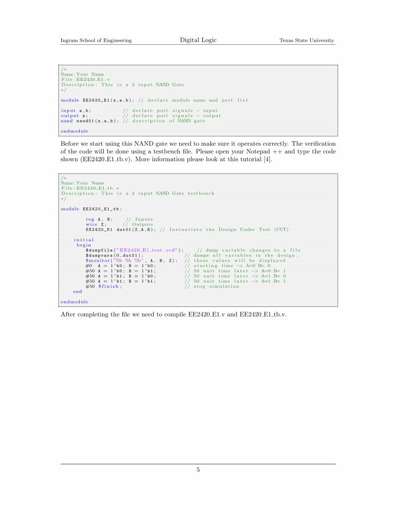
Open a command prompt window START Run cmd
Change directory u:
Go to your Lab folder where the files are located cd YourName Verilog
List the files ls or dir . You should see your files EE2420 E1.v and EE2420 E1.v
Compile the Verilog files iverilog EE2420 E1.v . No return display means NO ERROR.
Open your EE2420 E1.v file using Notepad and create a syntax error.
Compile the Verilog files again and record the error. All errors needs to be fixed.
Now you can compile your EE2420 E1 tb.v file iverilog EE2420 E1.v EE2420 E1 tb.v
If everything seems okay now we can test the design iverilog -o cool EE2420 E1.v EE2420 E1 tb.v
All the monitored values are dumped into file named ”cool”.
We need to see these values vvp cool
This will open the dumpfile EE2420 E1 test.vcd file and display the output.
Figure 3: Screenshot for the example 1
Using these values complete Table 1.
Table 1: NAND gate design verification
A B Z Zsim
0 0
0 1
1 0
1 1
If you want to see the GUI you may need to use GTKWave gtkwave EE2420 E1 test.vcd
6
Ingram School of Engineering Digital Logic Texas State University
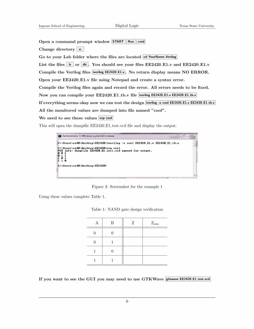
Figure 4: GTKWave Screenshot for the example 1
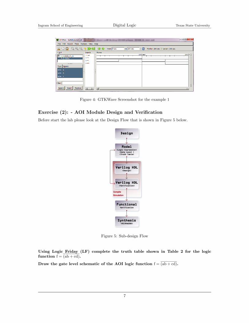
Exercise (2): - AOI Module Design and Verification
Before start the lab please look at the Design Flow that is shown in Figure 5 below.
Design
Model(Logic Expression)
(Gate Level )
(Truth Table)
Verilog HDL(Design)
Verilog HDL(Verification)
Simulation
Compile
Synthesis(MICROWIND)
FunctionalVerification
Figure 5: Sub-design Flow
Using Logic Friday (LF) complete the truth table shown in Table 2 for the logicfunction f = (ab + cd).
Draw the gate level schematic of the AOI logic function f = (ab + cd).
7
Ingram School of Engineering Digital Logic Texas State University
Table 2: Truth Table
a b c d f(LF) f(Verilog)
0 0 0 0
0 0 0 1
0 0 1 0
0 0 1 1
0 1 0 0
0 1 0 1
0 1 1 0
0 1 1 1
1 0 0 0
1 0 0 1
1 0 1 0
1 0 1 1
1 1 0 0
1 1 0 1
1 1 1 0
1 1 1 1
Copy and paste screenshot of Logic Friday truth table of your function in screen-shots.docx.
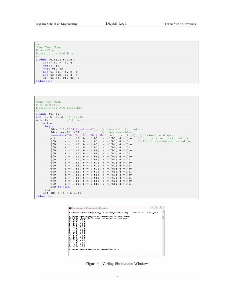
Using Notepad ++ create AOI.v and AOI tb.v files. Type the following Verilog codes,compile and simulate using iverilog and copy and paste screenshots of AOI.v andAOI tb.v, and simulation monitor output (Figure 6) files in screenshots.docx.
Label inputs, outputs, wires and gate labels (G1, G2, G3) in your AOI file schematicthat is described in subsection .
8
Ingram School of Engineering Digital Logic Texas State University
/∗Name : Your NameF i l e :AOI . vDesc r ip t i on : AOI F i l e∗/module AOI ( f , a , b , c , d ) ;
input a , b , c , d ;output f ;wire w1 , w2 ;and G1 ( w1 , a , b ) ;and G2 ( w2 , c , d ) ;or G3 ( f , w1 , w2 ) ;
endmodule
/∗Name : Your NameF i l e : AOI tb . vDesc r ip t i on : AOI testbench∗/module AOI_tb ;reg a , b , c , d ; // Inputswire f ; // Output
i n i t i a lbegin
$dumpfile ( ”AOI test . vcd” ) ; // Dump f i l e f o r va lues$dumpvars (0 , AOI_1 ) ; // Dump va r i a b l e s$monitor ( ”%b , %b , %b , %b | %b ” , a , b , c , d , f ) ; // va lues to d i sp l ay# 0 a = 1 ' b0 ; b = 1 ' b0 ; c =1 'b0 ; d =1 'b0 ; // inputs (Use truth tab l e )#50 a = 1 ' b0 ; b = 1 ' b0 ; c =1 'b0 ; d =1 'b1 ; // Use Notepad++ column ed i t o r#50 a = 1 ' b0 ; b = 1 ' b0 ; c =1 'b1 ; d =1 'b0 ;#50 a = 1 ' b0 ; b = 1 ' b0 ; c =1 'b1 ; d =1 'b1 ;#50 a = 1 ' b0 ; b = 1 ' b1 ; c =1 'b0 ; d =1 'b0 ;#50 a = 1 ' b0 ; b = 1 ' b1 ; c =1 'b0 ; d =1 'b1 ;#50 a = 1 ' b0 ; b = 1 ' b1 ; c =1 'b1 ; d =1 'b0 ;#50 a = 1 ' b0 ; b = 1 ' b1 ; c =1 'b1 ; d =1 'b1 ;#50 a = 1 ' b1 ; b = 1 ' b0 ; c =1 'b0 ; d =1 'b0 ;#50 a = 1 ' b1 ; b = 1 ' b0 ; c =1 'b0 ; d =1 'b1 ;#50 a = 1 ' b1 ; b = 1 ' b0 ; c =1 'b1 ; d =1 'b0 ;#50 a = 1 ' b1 ; b = 1 ' b0 ; c =1 'b1 ; d =1 'b1 ;#50 a = 1 ' b1 ; b = 1 ' b1 ; c =1 'b0 ; d =1 'b0 ;#50 a = 1 ' b1 ; b = 1 ' b1 ; c =1 'b0 ; d =1 'b1 ;#50 a = 1 ' b1 ; b = 1 ' b1 ; c =1 'b1 ; d =1 'b0 ;#50 a = 1 ' b1 ; b = 1 ' b1 ; c =1 'b1 ; d =1 'b1 ;#50 $ f i n i s h ;
endAOI AOI_1 ( f , a , b , c , d ) ;
endmodule
Figure 6: Verilog Simulation Window
9
Ingram School of Engineering Digital Logic Texas State University
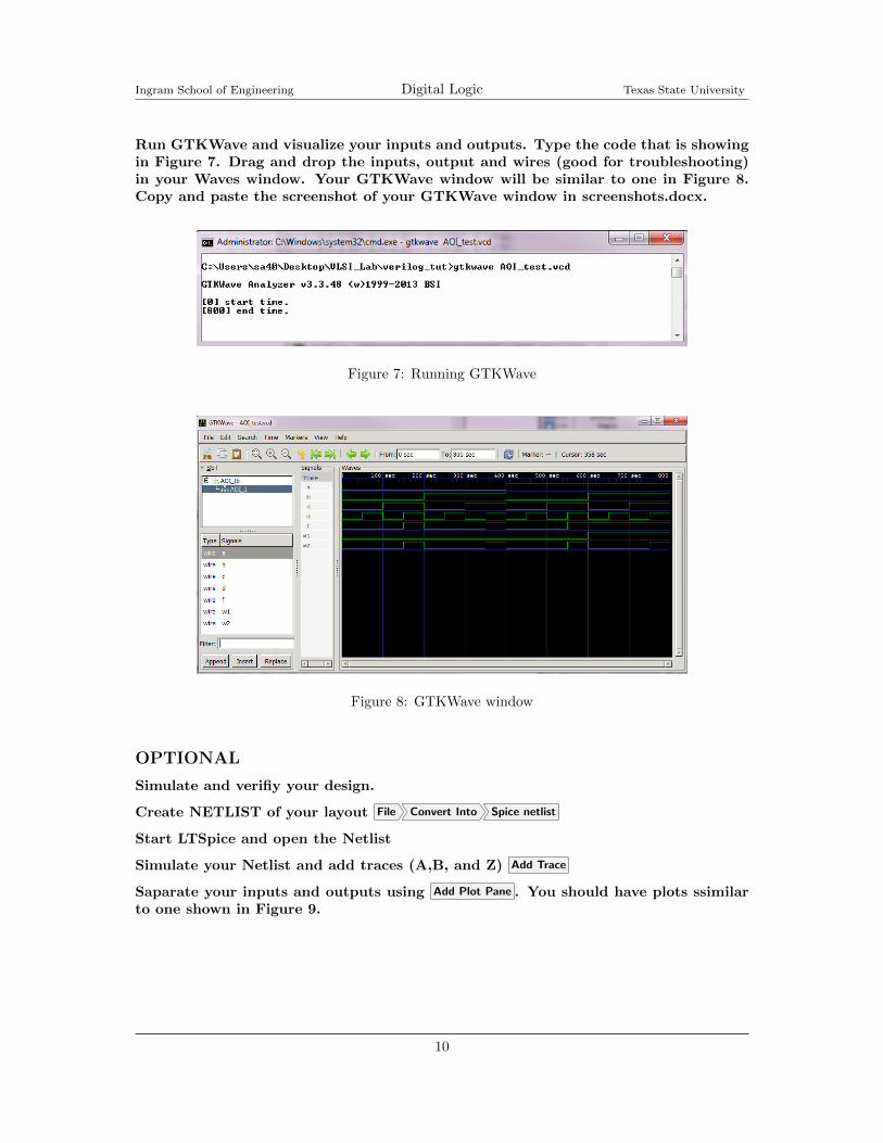
Run GTKWave and visualize your inputs and outputs. Type the code that is showingin Figure 7. Drag and drop the inputs, output and wires (good for troubleshooting)in your Waves window. Your GTKWave window will be similar to one in Figure 8.Copy and paste the screenshot of your GTKWave window in screenshots.docx.
Figure 7: Running GTKWave
Figure 8: GTKWave window
OPTIONAL
Simulate and verifiy your design.
Create NETLIST of your layout File Convert Into Spice netlist
Start LTSpice and open the Netlist
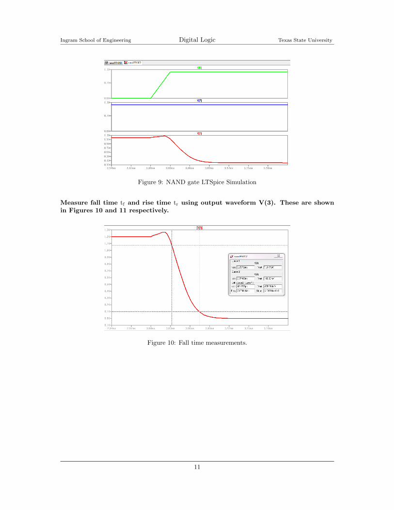
Simulate your Netlist and add traces (A,B, and Z) Add Trace
Saparate your inputs and outputs using Add Plot Pane . You should have plots ssimilarto one shown in Figure 9.
10
Ingram School of Engineering Digital Logic Texas State University
Figure 9: NAND gate LTSpice Simulation
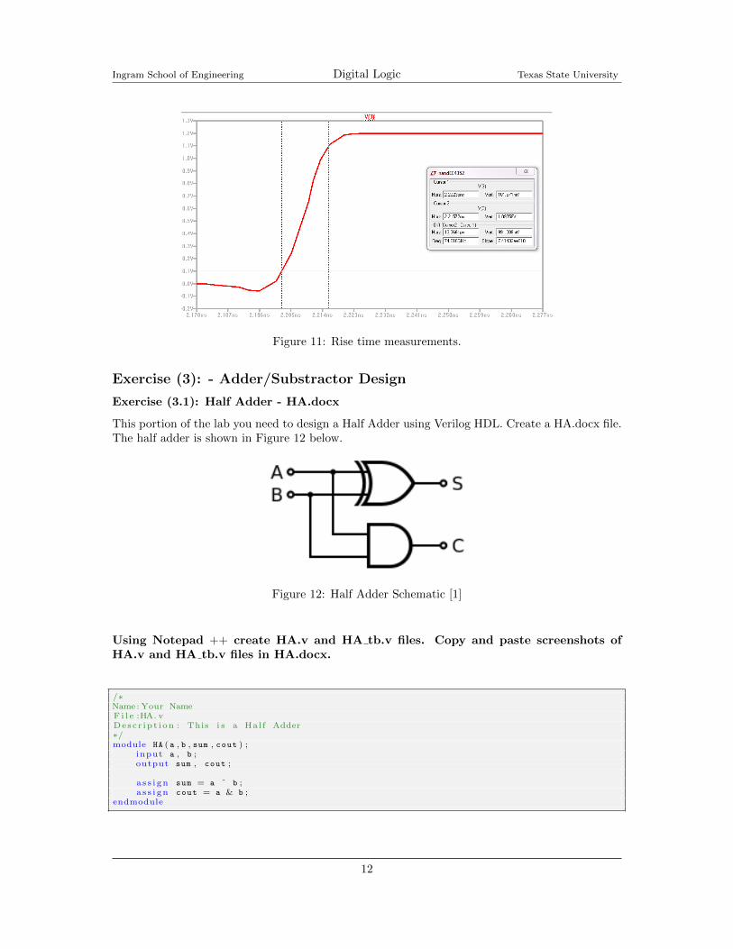
Measure fall time tf and rise time tr using output waveform V(3). These are shownin Figures 10 and 11 respectively.
Figure 10: Fall time measurements.
11
Ingram School of Engineering Digital Logic Texas State University
Figure 11: Rise time measurements.
Exercise (3): - Adder/Substractor Design
Exercise (3.1): Half Adder - HA.docx
This portion of the lab you need to design a Half Adder using Verilog HDL. Create a HA.docx file.The half adder is shown in Figure 12 below.
Figure 12: Half Adder Schematic [1]
Using Notepad ++ create HA.v and HA tb.v files. Copy and paste screenshots ofHA.v and HA tb.v files in HA.docx.
/∗Name : Your NameF i l e :HA. vDesc r ip t i on : This i s a Hal f Adder∗/module HA ( a , b , sum , cout ) ;
input a , b ;output sum , cout ;
a s s i gn sum = a ˆ b ;a s s i gn cout = a & b ;
endmodule
12
Ingram School of Engineering Digital Logic Texas State University
/∗Name : Your NameF i l e : HA tb . vDesc r ip t i on : This i s a Hal f Adder tes tbench∗/module HA_tb ;reg a , b ;wire sum , cout ;
i n i t i a lbegin
$dumpfile ( ”HA test . vcd” ) ;$dumpvars (0 , ha ) ;$monitor ( ”%b + %b = %b%b” , a , b , cout , sum ) ;#0 a = 1 ' b0 ; b = 1 ' b0 ;#50 a = 1 ' b0 ; b = 1 ' b1 ;#50 a = 1 ' b1 ; b = 1 ' b0 ;#50 a = 1 ' b1 ; b = 1 ' b1 ;#50 $ f i n i s h ;
endHA ha ( a , b , sum , cout ) ;
endmodule
Compile and Simulate your design as explained in Example 1. Copy and paste screen-shots of simulation window files in HA.docx.
Exercise (3.2): Full Adder - FA.docx
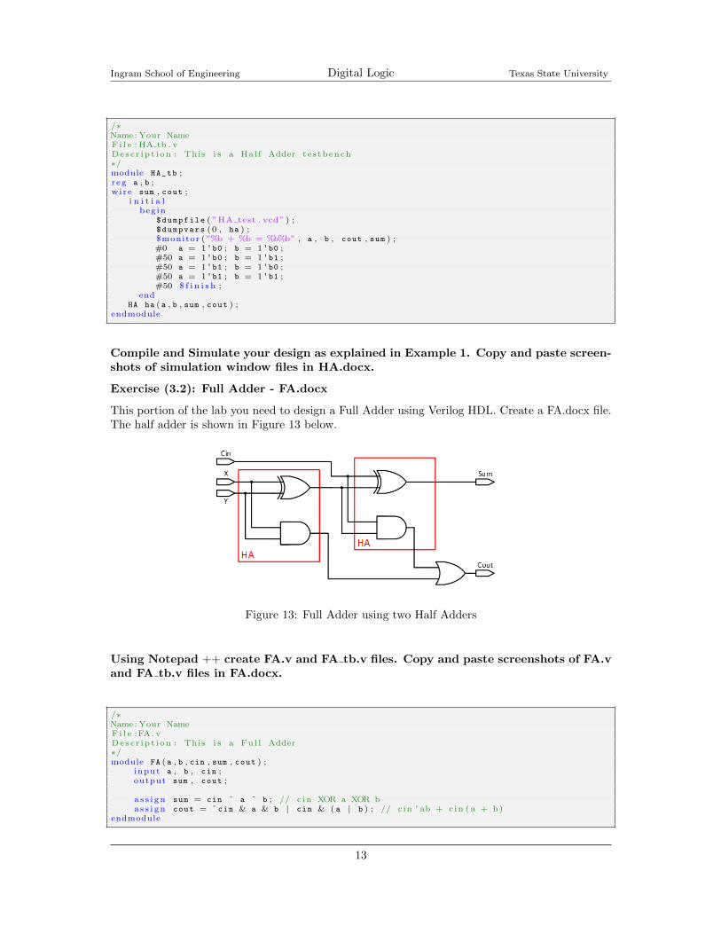
This portion of the lab you need to design a Full Adder using Verilog HDL. Create a FA.docx file.The half adder is shown in Figure 13 below.
Figure 13: Full Adder using two Half Adders
Using Notepad ++ create FA.v and FA tb.v files. Copy and paste screenshots of FA.vand FA tb.v files in FA.docx.
/∗Name : Your NameF i l e :FA. vDesc r ip t i on : This i s a Fu l l Adder∗/module FA ( a , b , cin , sum , cout ) ;
input a , b , cin ;output sum , cout ;
a s s i gn sum = cin ˆ a ˆ b ; // c in XOR a XOR bas s i gn cout = ˜ cin & a & b | cin & ( a | b ) ; // cin ' ab + c in ( a + b)
endmodule
13
Ingram School of Engineering Digital Logic Texas State University
/∗Name : Your NameF i l e : FA tb . vDesc r ip t i on : This i s a Fu l l Adder tes tbench∗/module FA_tb ;reg a , b , cin ;wire sum , cout ;
i n i t i a lbegin
$dumpfile ( ” s imple adder . vcd” ) ;$dumpvars (0 , fa ) ;$monitor ( ”%b + %b + %b = %b%b” , a , b , cin , cout , sum ) ;#0 a = 1 ' b0 ; b = 1 ' b0 ; cin = 1 ' b0 ; // c r ea t e the a l l p o s s i b l e t e s t va lues#50 a = 1 ' b0 ; b = 1 ' b0 ; cin = 1 ' b1 ;#50 $ f i n i s h ;
endFA fa01 ( a , b , cin , sum , cout ) ;
endmodule
Compile and Simulate your design as explained in Example 1. Copy and paste screen-shots of simulation window files in FA.docx.
Exercise (4): Four-Bit Ripple Carry Adder/Subtractor
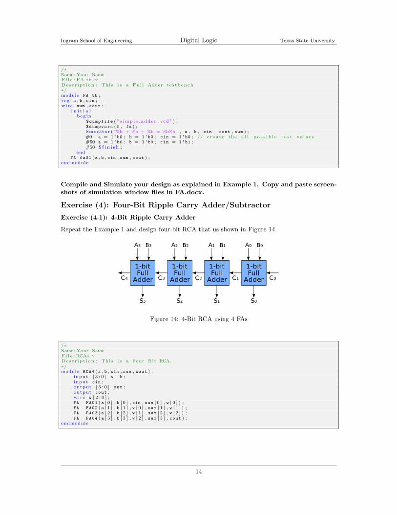
Exercise (4.1): 4-Bit Ripple Carry Adder
Repeat the Example 1 and design four-bit RCA that us shown in Figure 14.
Figure 14: 4-Bit RCA using 4 FAs
/∗Name : Your NameF i l e :RCA4. vDesc r ip t i on : This i s a Four Bit RCA.∗/module RCA4 ( a , b , cin , sum , cout ) ;
input [ 3 : 0 ] a , b ;input cin ;output [ 3 : 0 ] sum ;output cout ;wire w [ 2 : 0 ] ;FA FA01 ( a [ 0 ] , b [ 0 ] , cin , sum [ 0 ] , w [ 0 ] ) ;FA FA02 ( a [ 1 ] , b [ 1 ] , w [ 0 ] , sum [ 1 ] , w [ 1 ] ) ;FA FA03 ( a [ 2 ] , b [ 2 ] , w [ 1 ] , sum [ 2 ] , w [ 2 ] ) ;FA FA04 ( a [ 3 ] , b [ 3 ] , w [ 2 ] , sum [ 3 ] , cout ) ;
endmodule
14
Ingram School of Engineering Digital Logic Texas State University
/∗Name : Your NameF i l e : RCA4 tb . vDesc r ip t i on : This i s a Four−Bit RCA testbench∗/module RCA4_tb ;
reg [ 3 : 0 ] a , b ;reg cin ;wire [ 3 : 0 ] sum ;wire cout ;
i n i t i a lbegin
$dumpfile ( ”RCA test . vcd” ) ;$dumpvars (0 , RCA01 ) ;$monitor ( ”%d + %d + %d= %d%d” , a , b , cin , cout , sum ) ;#0 a = 4 ' d3 ; b = 4 ' b0000 ; cin = 1 ' b0 ;#50 a = 4 ' b0010 ; b = 4 ' b0100 ; cin = 1 ' b0 ;#50 a = 4 ' b0010 ; b = 4 ' b0100 ; cin = 1 ' b0 ; // Create more t e s t va lues#50 $ f i n i s h ;
end
RCA4 RCA01 ( a , b , cin , sum , cout ) ;
endmodule
Exercise (4.2): 4-Bit Ripple Carry Adder/Subtractor
Modify your RCA4.v file to RCA4 ADD SUB.v circuit.
References
[1] “Adder (electronics).” http://en.wikipedia.org/wiki/Adder. Accessed: 2014-10-30.
[2] “Verilog.” http://en.wikipedia.org/wiki/Verilog. Accessed: 2014-10-30.
[3] “Verilog primer.” http://www.verilogtutorial.info/. Accessed: 2014-10-30.
[4] “Asic world.” http://www.asic-world.com. Accessed: 2014-10-30.
15
Exercise (4.3): 16-Bit Ripple Carry Adder/Subtractor
Modify your RCA16.v file to RCA16 ADD SUB.v circuit.