Embed Size (px)
Citation preview
15.1
Unit 15
Common Hardware Components
15.2
Overview
• We will explore some common digital hardware components that are used to build larger devices such as a processor
• These components include:
– Multi-bit (wide) muxes
– Register with enables
– Counters
– Arithmetic and Logic Units
– Multipliers
15.3
WIDE MUXES
15.4
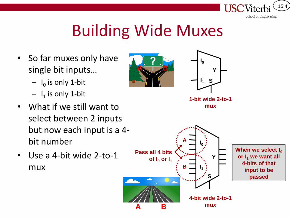
Building Wide Muxes
• So far muxes only have single bit inputs…– I0 is only 1-bit
– I1 is only 1-bit
• What if we still want to select between 2 inputs but now each input is a 4-bit number
• Use a 4-bit wide 2-to-1 mux I1
I0
S
Y
I0
I1
Y
S
Pass all 4 bits
of I0 or I1
When we select I0or I1 we want all
4-bits of that
input to be
passed
1-bit wide 2-to-1
mux
4-bit wide 2-to-1
mux
A
B
A B
A B
15.5
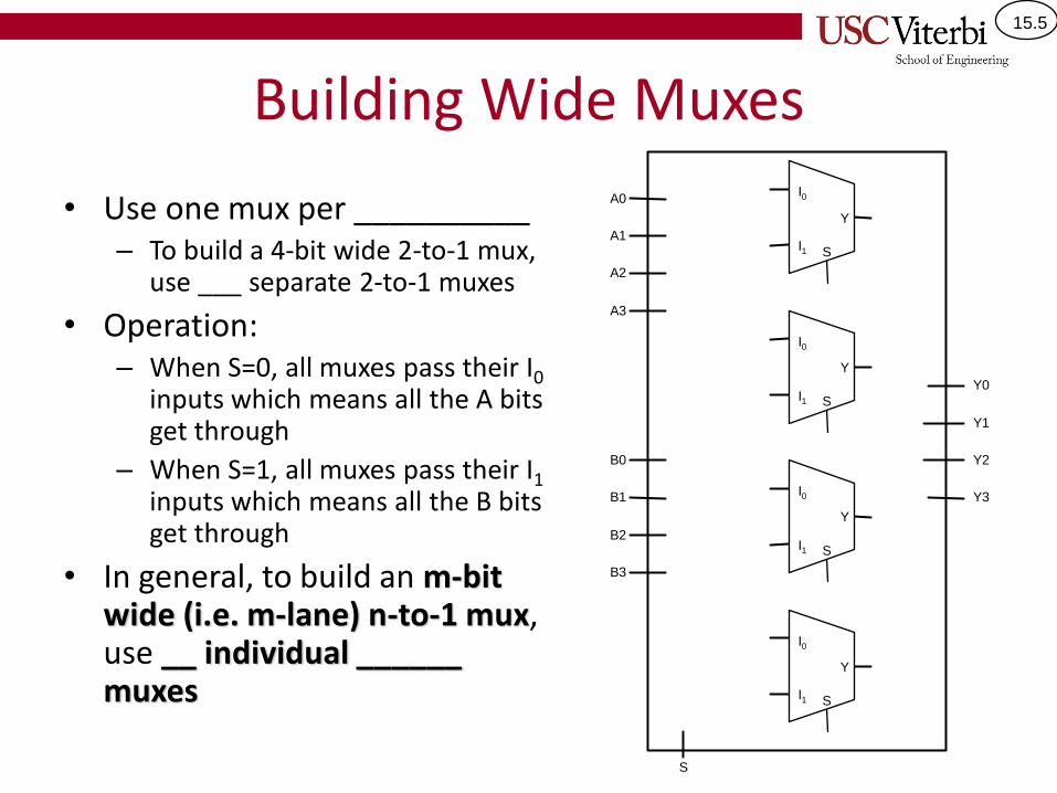
Building Wide Muxes
• Use one mux per __________– To build a 4-bit wide 2-to-1 mux,
use ___ separate 2-to-1 muxes
• Operation:– When S=0, all muxes pass their I0
inputs which means all the A bits get through
– When S=1, all muxes pass their I1
inputs which means all the B bits get through
• In general, to build an m-bit wide (i.e. m-lane) n-to-1 mux, use __ individual ______ muxes
I1
Y
S
I0
I1
Y
S
I0
I1
Y
S
I0
I1
Y
S
I0
B0
A0
A1
A2
A3
B1
B2
B3
S
Y0
Y1
Y2
Y3
15.6
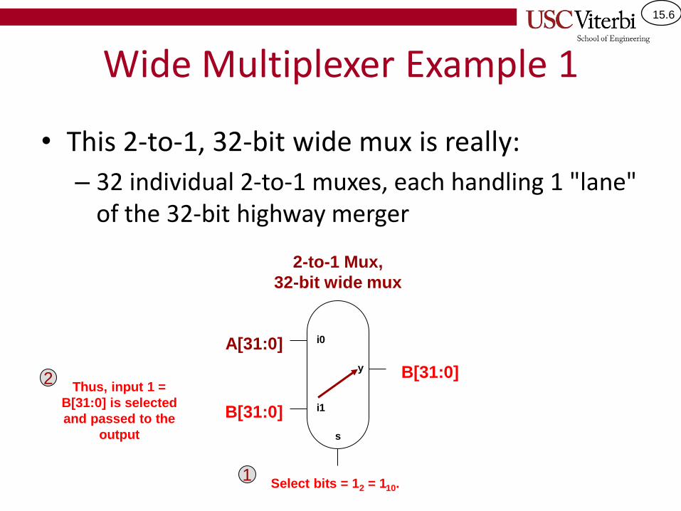
Wide Multiplexer Example 1
• This 2-to-1, 32-bit wide mux is really:
– 32 individual 2-to-1 muxes, each handling 1 "lane" of the 32-bit highway merger
A[31:0]
Thus, input 1 =
B[31:0] is selected
and passed to the
output
Select bits = 12 = 110.1
2
2-to-1 Mux,
32-bit wide mux
i0
i1
y
s
B[31:0]
B[31:0]
15.7
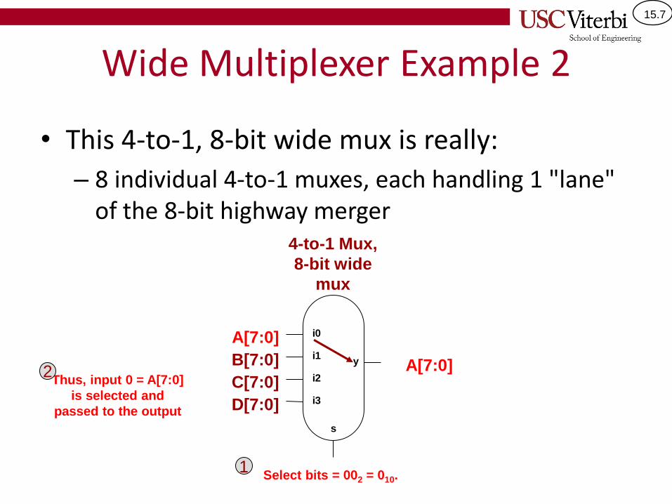
Wide Multiplexer Example 2
• This 4-to-1, 8-bit wide mux is really:
– 8 individual 4-to-1 muxes, each handling 1 "lane" of the 8-bit highway merger
A[7:0]
Thus, input 0 = A[7:0]
is selected and
passed to the output
Select bits = 002 = 010.1
2
4-to-1 Mux,
8-bit wide
mux
i0
i1
i2
i3
y
s
B[7:0]
C[7:0]
D[7:0]
A[7:0]
15.8
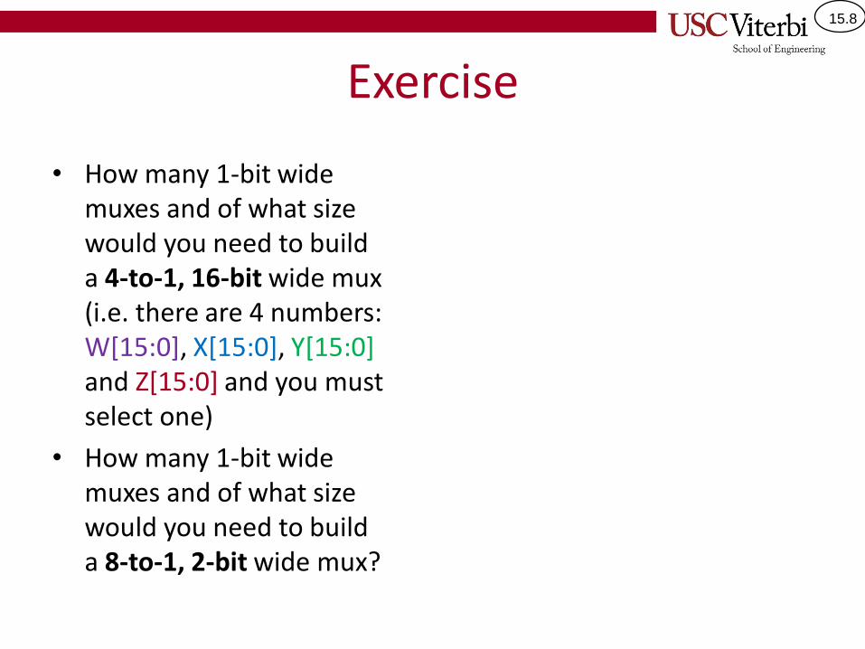
Exercise
• How many 1-bit wide muxes and of what size would you need to build a 4-to-1, 16-bit wide mux (i.e. there are 4 numbers: W[15:0], X[15:0], Y[15:0]and Z[15:0] and you must select one)
• How many 1-bit wide muxes and of what size would you need to build a 8-to-1, 2-bit wide mux?
15.9
REGISTER WITH ENABLESUsing muxes to control when register save data
15.10
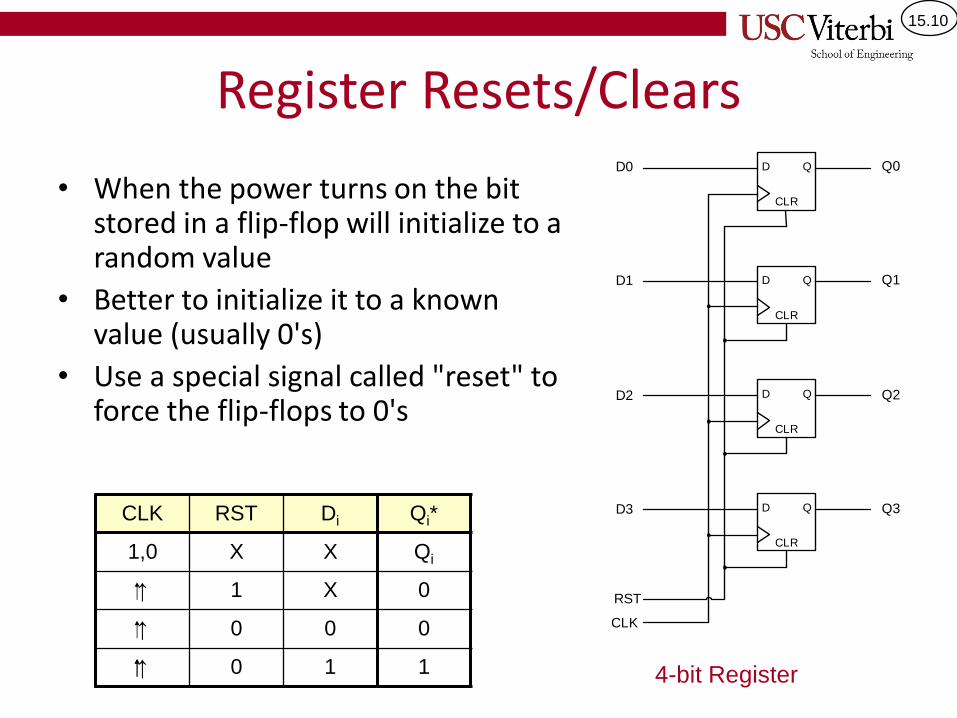
Register Resets/Clears
• When the power turns on the bit stored in a flip-flop will initialize to a random value
• Better to initialize it to a known value (usually 0's)
• Use a special signal called "reset" to force the flip-flops to 0's
CLK RST Di Qi*
1,0 X X Qi
↑ 1 X 0
↑ 0 0 0
↑ 0 1 1 4-bit Register
D Q
CLR
RST
D Q
CLR
D Q
CLR
D Q
CLR
CLK
D3
D2
D1
D0
Q3
Q2
Q1
Q0
15.11
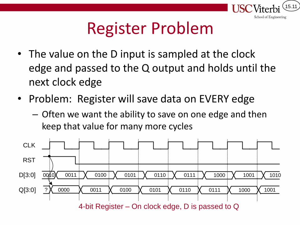
Register Problem
• The value on the D input is sampled at the clock edge and passed to the Q output and holds until the next clock edge
• Problem: Register will save data on EVERY edge
– Often we want the ability to save on one edge and then keep that value for many more cycles
4-bit Register – On clock edge, D is passed to Q
CLK
RST
D[3:0]
Q[3:0] 0000
0011 0100 0101 0110 0111 1000 1001 10100010
0011 0100 0101 0110 0111 1000 1001?
15.12
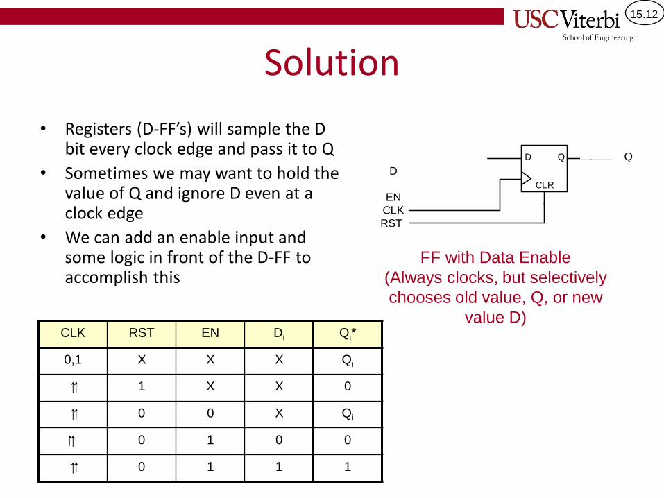
Solution
• Registers (D-FF’s) will sample the D bit every clock edge and pass it to Q
• Sometimes we may want to hold the value of Q and ignore D even at a clock edge
• We can add an enable input and some logic in front of the D-FF to accomplish this
CLK RST EN Di Qi*
0,1 X X X Qi
↑ 1 X X 0
↑ 0 0 X Qi
↑ 0 1 0 0
↑ 0 1 1 1
FF with Data Enable
(Always clocks, but selectively
chooses old value, Q, or new
value D)
D Q
CLR
D
Q0
1
Y
S
EN
CLK
RST
15.13
D Q
CLR
D
Q0
1
Y
S
EN
CLK
RST
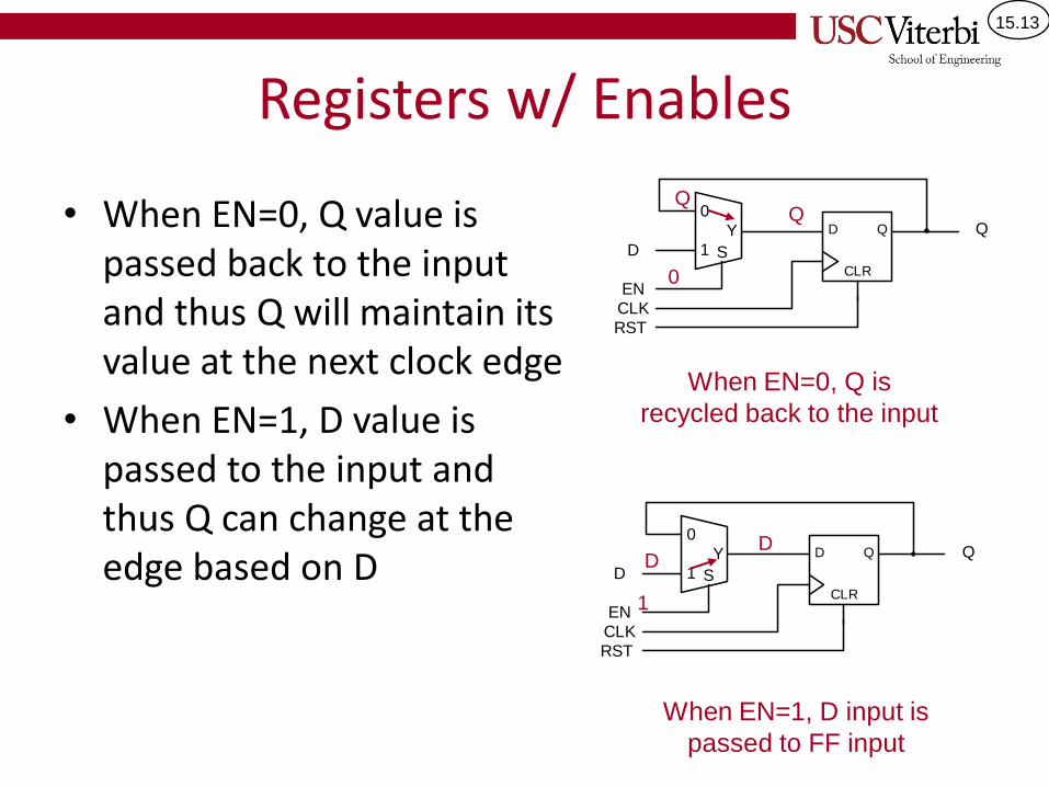
Registers w/ Enables
• When EN=0, Q value is passed back to the input and thus Q will maintain its value at the next clock edge
• When EN=1, D value is passed to the input and thus Q can change at the edge based on D
When EN=0, Q is
recycled back to the input
1
When EN=1, D input is
passed to FF input
DD
D Q
CLR
D
Q0
1
Y
S
EN
CLK
RST
0
15.14
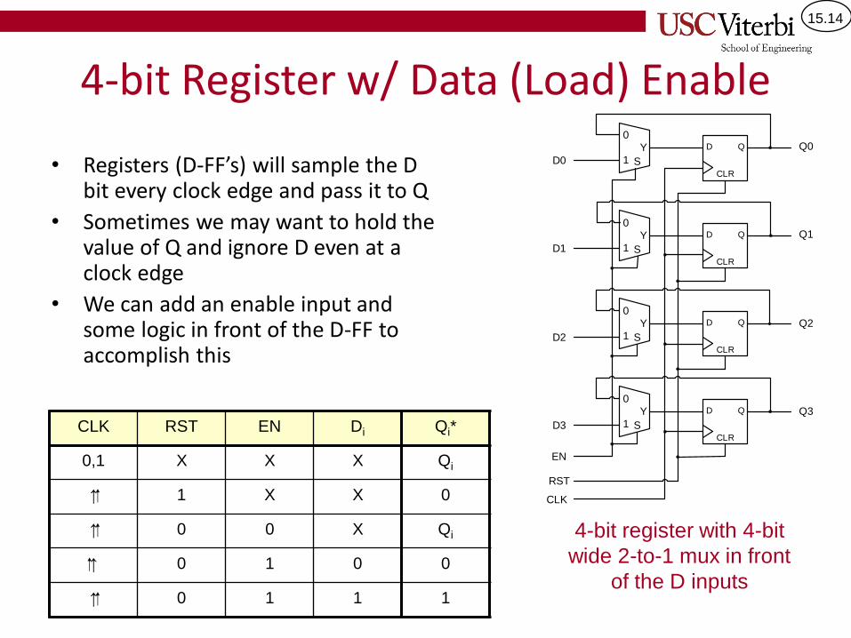
4-bit Register w/ Data (Load) Enable
• Registers (D-FF’s) will sample the D bit every clock edge and pass it to Q
• Sometimes we may want to hold the value of Q and ignore D even at a clock edge
• We can add an enable input and some logic in front of the D-FF to accomplish this
CLK RST EN Di Qi*
0,1 X X X Qi
↑ 1 X X 0
↑ 0 0 X Qi
↑ 0 1 0 0
↑ 0 1 1 1
4-bit register with 4-bit
wide 2-to-1 mux in front
of the D inputs
D Q
CLR
RST
D Q
CLR
D Q
CLR
D Q
CLR
CLK
D3
D2
D1
D0
Q3
Q2
Q1
Q00
1
Y
S
0
1
Y
S
0
1
Y
S
0
1
Y
S
EN
15.15
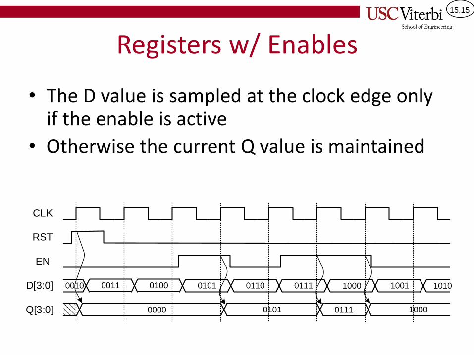
Registers w/ Enables
• The D value is sampled at the clock edge only if the enable is active
• Otherwise the current Q value is maintained
CLK
RST
EN
D[3:0]
Q[3:0] 0000 0101 0111 1000
0011 0100 0101 0110 0111 1000 1001 10100010

15.16
COUNTERS
15.17
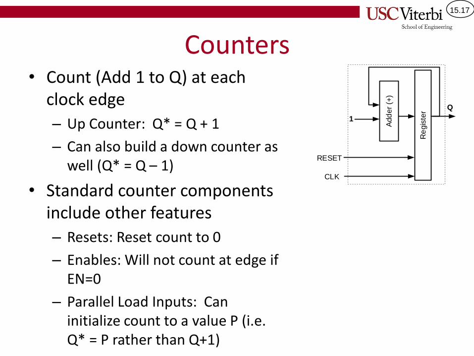
Counters• Count (Add 1 to Q) at each
clock edge
– Up Counter: Q* = Q + 1
– Can also build a down counter as well (Q* = Q – 1)
• Standard counter components include other features
– Resets: Reset count to 0
– Enables: Will not count at edge if EN=0
– Parallel Load Inputs: Can initialize count to a value P (i.e. Q* = P rather than Q+1)
Re
gis
ter
1
Add
er
(+)
Q
RESET
CLK
15.18
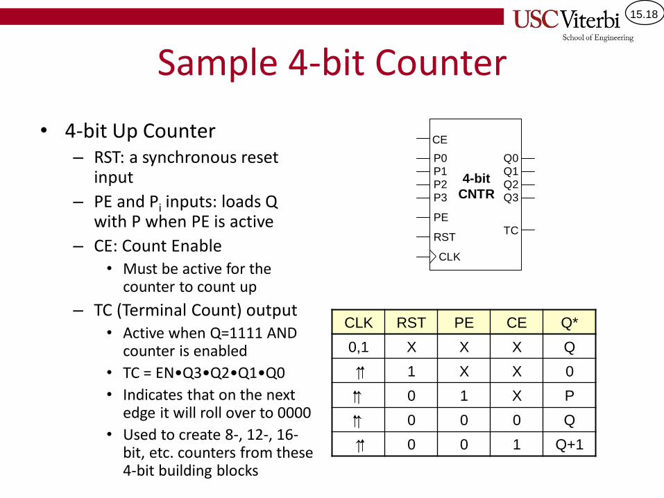
Sample 4-bit Counter
• 4-bit Up Counter– RST: a synchronous reset
input
– PE and Pi inputs: loads Q with P when PE is active
– CE: Count Enable • Must be active for the
counter to count up
– TC (Terminal Count) output • Active when Q=1111 AND
counter is enabled
• TC = EN•Q3•Q2•Q1•Q0
• Indicates that on the next edge it will roll over to 0000
• Used to create 8-, 12-, 16-bit, etc. counters from these 4-bit building blocks
CLK RST PE CE Q*
0,1 X X X Q
↑ 1 X X 0
↑ 0 1 X P
↑ 0 0 0 Q
↑ 0 0 1 Q+1
CLK
P0
P1
P2
P3
Q0
Q1
Q2
Q3
TC
PE
RST
4-bit
CNTR
CE
15.19
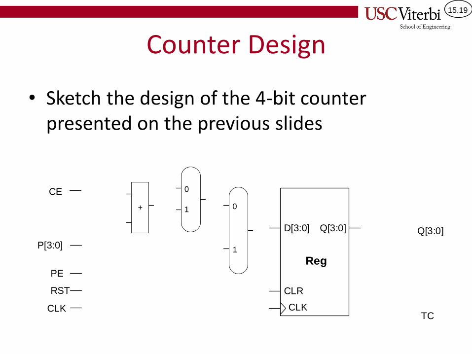
Counter Design
• Sketch the design of the 4-bit counter presented on the previous slides
CLK
D[3:0] Q[3:0]
Reg
CLR
P[3:0]
PE
RST
CE
CLK
Q[3:0]
TC
+
0
1 0
1
15.20
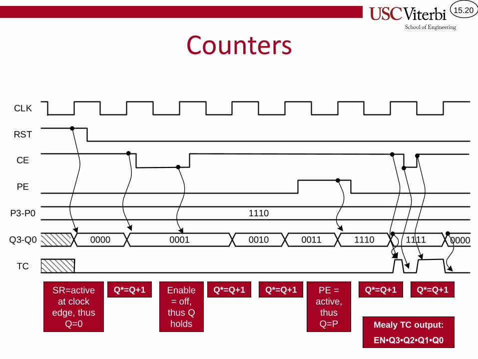
Counters
SR=active
at clock
edge, thus
Q=0
Q*=Q+1 Enable
= off,
thus Q
holds
PE =
active,
thus
Q=P
Q*=Q+1 Q*=Q+1 Q*=Q+1 Q*=Q+1
Mealy TC output:
EN•Q3•Q2•Q1•Q0
0000
CLK
RST
CE
PE
P3-P0
Q3-Q0 0001 0010 0011 1110 1111
TC
1110
1 0000
15.21
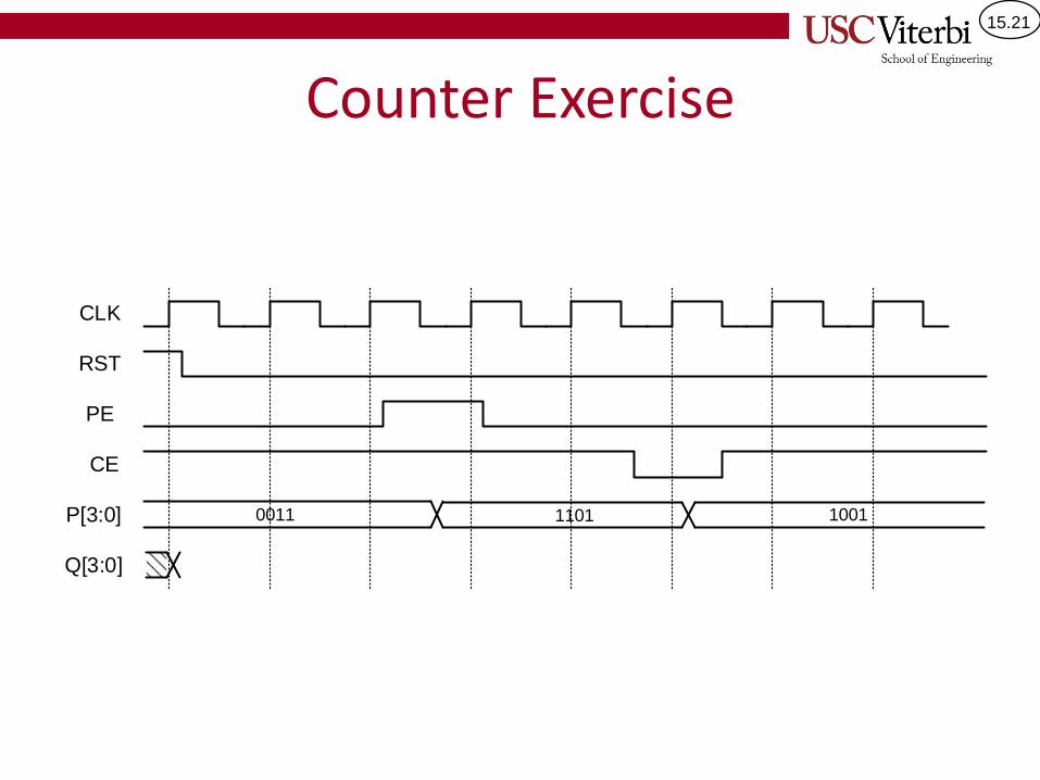
Counter Exercise
CLK
RST
PE
CE
P[3:0]
Q[3:0]
0011 1101 1001

15.22
ALUS
15.23
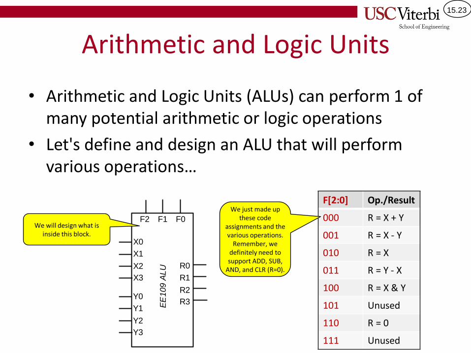
Arithmetic and Logic Units
• Arithmetic and Logic Units (ALUs) can perform 1 of many potential arithmetic or logic operations
• Let's define and design an ALU that will perform various operations…
X0
X1
X2
X3
Y0
Y1
Y2
Y3
EE
109 A
LU R0
R1
R2
R3
F2 F1 F0
F[2:0] Op./Result
000 R = X + Y
001 R = X - Y
010 R = X
011 R = Y - X
100 R = X & Y
101 Unused
110 R = 0
111 Unused
We will design what is inside this block.
We just made up these code
assignments and the various operations.
Remember, we definitely need to support ADD, SUB,
AND, and CLR (R=0).
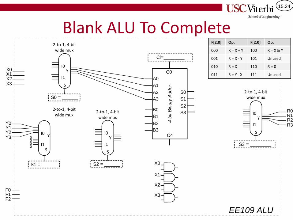
15.24
A0
A1
A2
A3
B0
B1
B2
B3
4-b
it B
inary
Add
er
C0
C4
S0
S1
S2
S3
S
I0 Y
I1
2-to-1, 4-bit wide mux
X0X1X2X3
Y0Y1Y2Y3
R0R1R2R3
F0F1F2
S
I0Y
I1
2-to-1, 4-bit wide mux
S
I0Y
I1
2-to-1, 4-bit wide mux
X0
X1
X2
X3
Ci=________
S1 = ______ S2 = ______
S3 = ________
0000
EE109 ALU
EE109 ALU
S
I0Y
I1
2-to-1, 4-bit wide mux
S0 = ______
Blank ALU To CompleteF[2:0] Op. F[2:0] Op.
000 R = X + Y 100 R = X & Y
001 R = X - Y 101 Unused
010 R = X 110 R = 0
011 R = Y - X 111 Unused
15.25
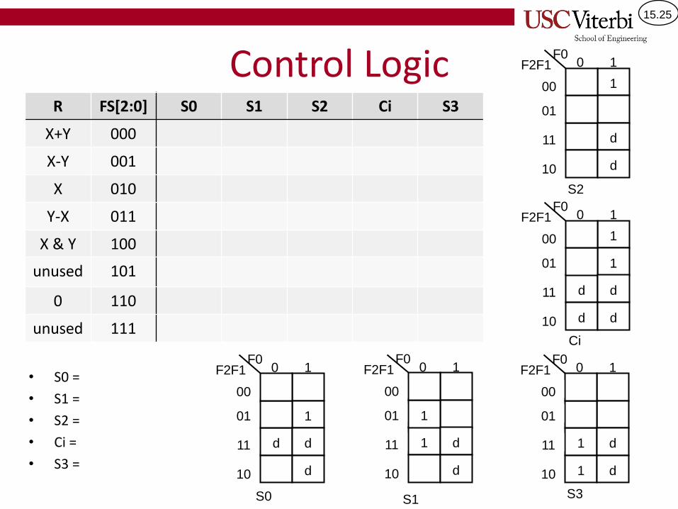
Control Logic
• S0 =
• S1 =
• S2 =
• Ci =
• S3 =
R FS[2:0] S0 S1 S2 Ci S3
X+Y 000
X-Y 001
X 010
Y-X 011
X & Y 100
unused 101
0 110
unused 111
100
01
11
10
0F0
F2F1
d
d
1
1
d
1
00
01
11
10
0F0
F2F1
d
d d
1
1
00
01
11
10
0F0
F2F1
d
1 d
1
d
1
00
01
11
10
0F0
F2F1
d
d
1
1
1
00
01
11
10
0F0
F2F1
d
d
1
S0 S1
S2
Ci
S3
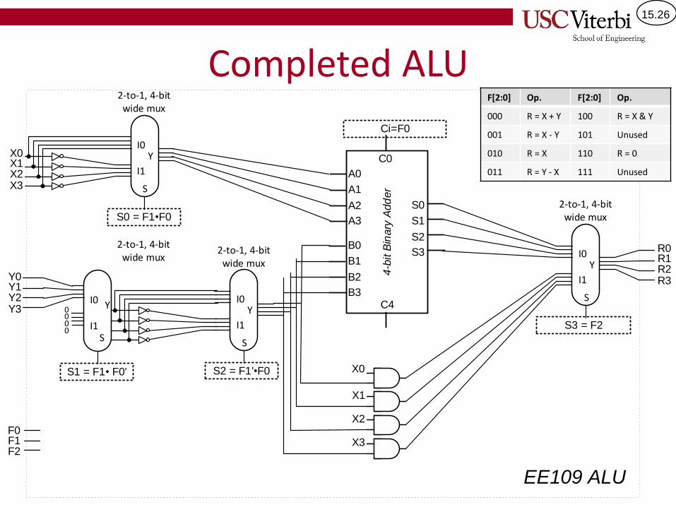
15.26
A0
A1
A2
A3
B0
B1
B2
B3
4-b
it B
inary
Add
er
C0
C4
S0
S1
S2
S3
S
I0 Y
I1
2-to-1, 4-bit wide mux
X0X1X2X3
Y0Y1Y2Y3
R0R1R2R3
F0F1F2
S
I0Y
I1
2-to-1, 4-bit wide mux
S
I0Y
I1
2-to-1, 4-bit wide mux
X0
X1
X2
X3
S1 = F1 F0' S2 = F1' F0
S3 = F2
0000
EE109 ALU
EE109 ALU
S
I0Y
I1
2-to-1, 4-bit wide mux
S0 = F1 F0
Ci=F0
Completed ALUF[2:0] Op. F[2:0] Op.
000 R = X + Y 100 R = X & Y
001 R = X - Y 101 Unused
010 R = X 110 R = 0
011 R = Y - X 111 Unused
15.27
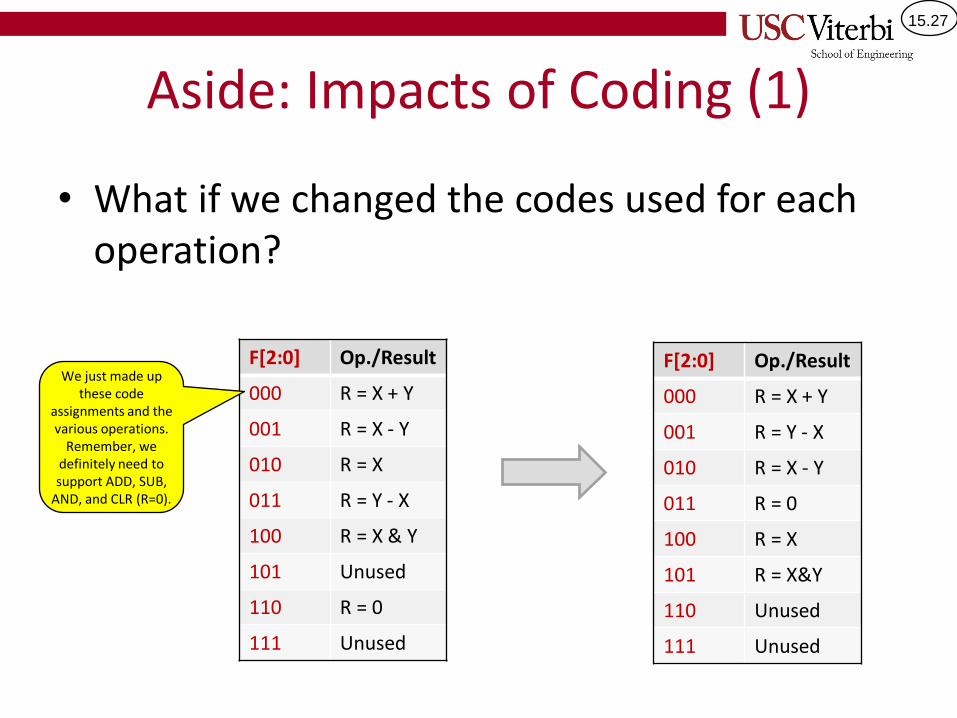
Aside: Impacts of Coding (1)
• What if we changed the codes used for each operation?
F[2:0] Op./Result
000 R = X + Y
001 R = X - Y
010 R = X
011 R = Y - X
100 R = X & Y
101 Unused
110 R = 0
111 Unused
We just made up these code
assignments and the various operations.
Remember, we definitely need to support ADD, SUB,
AND, and CLR (R=0).
F[2:0] Op./Result
000 R = X + Y
001 R = Y - X
010 R = X - Y
011 R = 0
100 R = X
101 R = X&Y
110 Unused
111 Unused
15.28
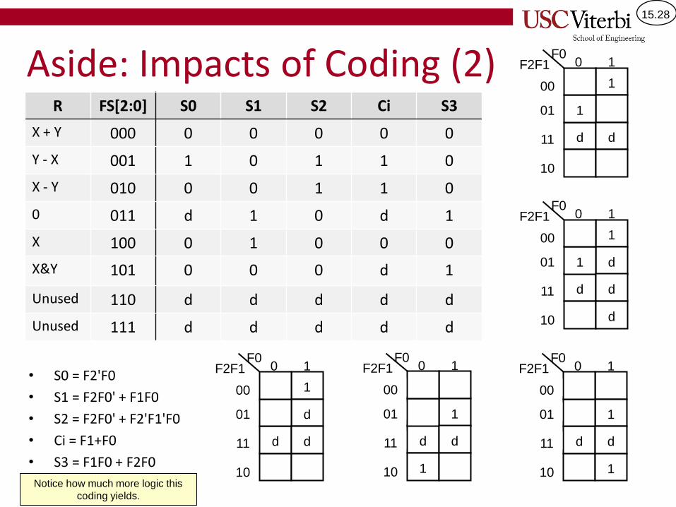
Aside: Impacts of Coding (2)
• S0 = F2'F0
• S1 = F2F0' + F1F0
• S2 = F2F0' + F2'F1'F0
• Ci = F1+F0
• S3 = F1F0 + F2F0
R FS[2:0] S0 S1 S2 Ci S3
X + Y 000 0 0 0 0 0
Y - X 001 1 0 1 1 0
X - Y 010 0 0 1 1 0
0 011 d 1 0 d 1
X 100 0 1 0 0 0
X&Y 101 0 0 0 d 1
Unused 110 d d d d d
Unused 111 d d d d d
1
d
1
00
01
11
10
0F0
F2F1
d
1
1
d
d1
00
01
11
10
0F0
F2F1
d
d
1
d
1
00
01
11
10
0F0
F2F1
d
1
1
1
d
d
00
01
11
10
0F0
F2F1
d
1
d
1
00
01
11
10
0F0
F2F1
d
1
1
Notice how much more logic this
coding yields.