Embed Size (px)
Citation preview

1
EE 551Linear Integrated Circuits
David W. GrahamWest Virginia University
Lane Department of Computer Science and Electrical Engineering© David W. Graham, 2009-2013
2
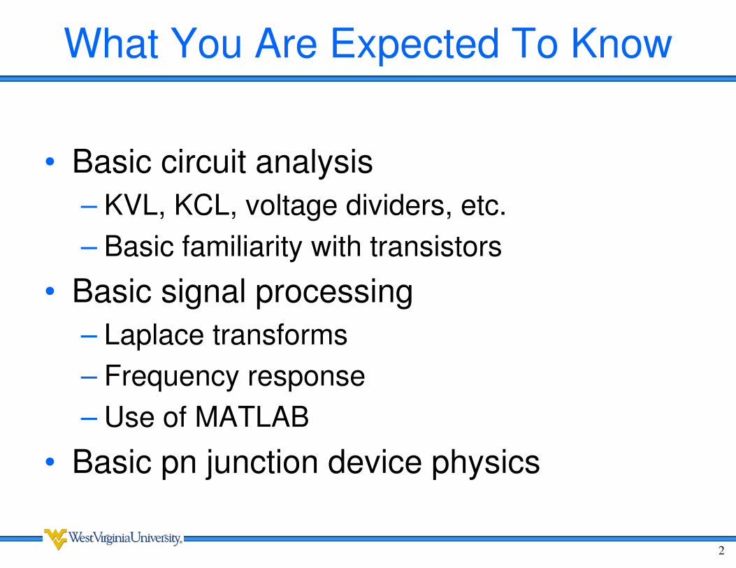
What You Are Expected To Know
• Basic circuit analysis
– KVL, KCL, voltage dividers, etc.
– Basic familiarity with transistors
• Basic signal processing
– Laplace transforms
– Frequency response
– Use of MATLAB
• Basic pn junction device physics

3
How To Do Well in EE 551
• Come to Class– Pay attention– Take good notes– If I talk about it in class, then it is probably important– Do whatever you have to do to stay awake
• Do the homework problems– Do them again– Do them yet again (These problems are typical of analog IC problems)– Hide the solutions when you do them– Write out every step– Do not assume that if you can follow the solutions you will be able to do
the problems at test time
• Start early on the projects– Do the individual parts as they are covered in class– Do not wait until the last minute
• If you do not understand, then ask questions– In class– In office hours

4
Analyze and Design
Vin+Vin-
Vout

5
What Design Really Looks Like

6
Why Analog?
• Can be much less power than digital
• Can perform many computations faster and more efficiently than digital
• Must be used to interface with outside world
• ~20% of IC market since 1970

7
Why This Class Is Important To You
“If you’re a 20- to 30-year-old analog engineer, you’re sitting pretty right now. It’s a buyer’s market for you.”
- Freescale Semiconductor
From IEEE Spectrum, Aug. 2008

8
Why This Class Is Important To You
Even if you have no plans of going into analog IC design, you will have a hard time not using analog ICs in your work. Understanding the guts of analog IC design will enable you to better evaluate their performance and choose the right parts.

9
The Future of Analog
“Analog chips enable computers to interact with the physical world – to see, listen, touch. . .the next ten years will see a shift in emphasis to analog technologies. . . In the coming years, look for analog –not digital – chips to attract the new talent and investment. . .”
- Red Herring Magazine, February 2003

10
Why Analog for Linear Systems?
Sensor /Transducer
µProcessor(Digital)
OutsideWorld
Interface(Analog)
Interface(Analog)
OutsideWorld
Amplifiers, Filters, Data Converters
The real world is analog, so if we need to interface with it, then we must have analog circuitry.

11
Why Integrated Circuits?
• Cheaper (and easier to mass produce)
• Smaller
• Reduces power
• Keeps everything contained– Reduces noise
– Reduces coupling from the environment
• Need a large number of transistors to perform real-world computations/tasks
• Allows a high density of circuit elements (therefore, VLSI reduces costs)

12
Difference Between Discrete and IC Design
Analog ICs Discrete Analog
Device Size and Values
Relatively Small
ex. Capacitors 10fF-100pF
Large
ex. Capacitors 100pF-100µF
ResistorsMostly bad
Very expensive (large real estate)
Easy to Use
Cheap
InductorsOnly feasible for very high frequencies
Extremely expensive
Use when needed
ParasiticsVery big concern
Seriously alter system performance
Exist, but rarely affect performance
(Large size of devices and currents)
Matching
Difficult to deal with
Major concern
Stuck with whatever was fabricated
ex. 50% mismatch is not uncommon
Concern
Can more easily match/replace
PowerEfficient
(Small currents pA-mA)
Use more power
(Large currents >mA)

13
Process Considerations
• What processes are…– A specific technology for producing integrated circuits– Typically specified by their
• Type (bipolar, CMOS, or BiCMOS)• Minimum device size (length) for CMOS (e.g. 0.5µm, 0.35µm)• Various other parameters (e.g. maximum/supply voltage, intended
disposition – digital or mixed-signal, etc.)
– Fabricated by a trusted foundry (e.g. AMS, TSMC, etc.)
• Everything is geared towards a digital process– Processes not designed with analog in mind– Easiest (best method / most flexible) to design with standard
process rules– Typically not able to construct many analog circuits in a brand
new process

14
Moore’s Law and Its Affect on CMOS Processes
• Moore’s Law (1965)– The number of transistors on an
integrated circuit doubles every (approximately) 18-24 months
• Processes vs. time– Introduction of a new process
approximately every two years• This shrinks the transistors, so more
can fit in a given space• Minimum transistor length decreases
over time• Most digital circuits are purely
[minimum-sized] transistors
– Greatly speeds up processing speeds– Greatly reduces power consumption– Intended to reduce cost, as well (but
new processes can be quite expensive)

15
Effect of Changing Processes
What changing processes mean (for design)• Supply voltages drop (big difference)
– e.g. 0.5µm Vdd = 3.3V; 0.18µm Vdd = 1.8V– New techniques for reduced operating range
• Device sizes– Transistor sizes decrease with every process– Capacitors may not
• Short channel effects– Traditional MOSFET models are a poor fit to small devices
• Varying design rules from process to process (submicron processes)– Must relearn “design rules” for each process– Specific rules to make sure nothing breaks

16
Process Type
Bipolar vs. CMOS
Pros for Bipolar• Work well for analog• High gain• High speed
Pros for CMOS• Cheap, cheap, cheap!• Scales nicely with Moore’s Law• Mixed-signal ICs (SOC)

17
System-On-A-Chip (SOC)
The real reason why CMOS dominates analog ICs – Systems on a chip
Analog Digital
Complete Integrated Circuit
Real designs include both analog and digital portions• Digital Portion
– Scales nicely with Moore’s Law– Straightforward design procedures– Uses mostly small transistors (can really pack them in) and very few
capacitors
• Analog Portion– Scaling mostly comes through ingenuity– No straightforward/automated design procedures– Uses often relatively large transistors and capacitors– Consumes a large amount of the chip real estate and design time
Easier, cheaper, and better to do a
complete design on a single chip.
18
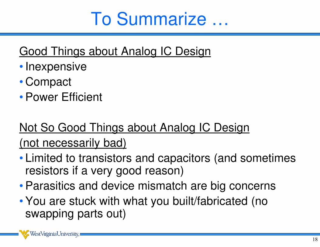
To Summarize …
Good Things about Analog IC Design
• Inexpensive
• Compact
• Power Efficient
Not So Good Things about Analog IC Design
(not necessarily bad)
• Limited to transistors and capacitors (and sometimes resistors if a very good reason)
• Parasitics and device mismatch are big concerns
• You are stuck with what you built/fabricated (no swapping parts out)
19
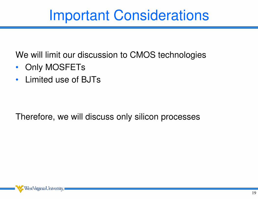
Important Considerations
We will limit our discussion to CMOS technologies
• Only MOSFETs
• Limited use of BJTs
Therefore, we will discuss only silicon processes

20
Linear Integrated Circuits
• Circuits and systems are linear only over a specific range• We will constantly talk about
– Large-signal operation• Nonlinear equations
• DC operating point, bias conditions
– Small-signal analysis• Linear equations
• Amplification region
• Every circuit must be analyzed with both the large- and small-signal analyses
Sensor /Transducer
µProcessor(Digital)
OutsideWorld
Interface(Analog)
Interface(Analog)
OutsideWorld
Amplifiers, Filters, Data Converters

21
Large-Signal vs. Small-Signal
Vout
Vin
Typical Amplifier Transfer Function
Linear, high-gain region (amplifier)
Nonlinear portions
Gain = Slope
• Must first do a large-signal analysis to get the amplifier into range– Bias in the amplification region– DC operating point (DC voltages and currents) from the large-signal operation
• Once in the amplification region, assume a small-signal input– Everything will stay within the linear region / linear range– Linear, time-invariant (LTI) analysis applies

22
Large-Signal vs. Small-Signal
Vout
Vin
Typical Amplifier Transfer Function
DC Operating Point
• Large signal (Biases / DC conditions)– Moves amplifier into range– Amplifier is now ready to perform amplification
• Small signal (AC inputs / outputs)– Small sinusoidal inputs makes bigger sinusoidal outputs
23
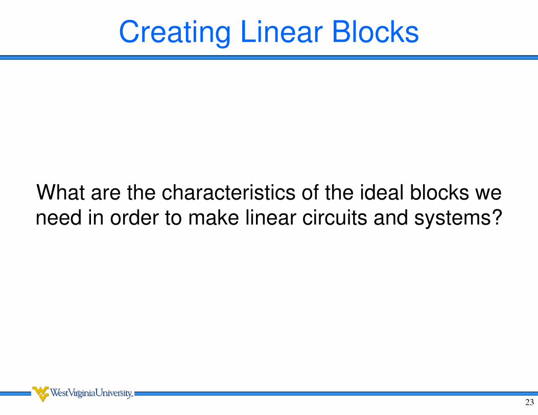
Creating Linear Blocks
What are the characteristics of the ideal blocks we need in order to make linear circuits and systems?

24
Input / Output Relationships
Device Zin Zout Reason
Independent Voltage
Source- 0Ω
0V output no voltage drop; no resistance
0V output replace with a short circuit
Independent Current
Source- ∞Ω
0A output no current flows; infinite resistance
0A output replace with an open circuit
Voltmeter ∞Ω -Minimizes loading effects
No resistance in parallel
Ammeter 0Ω -Minimizes loading effects
No resistance in series
Voltage-Controlled
Voltage Source (VCVS)∞Ω 0Ω
Voltage-Controlled
Current Source (VCCS)∞Ω ∞Ω
Current-Controlled
Voltage Source (CCVS)0Ω 0Ω
Current-Controlled
Current Source (CCCS)0Ω ∞Ω
25
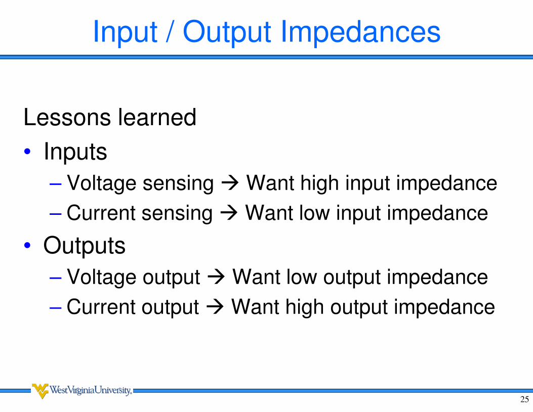
Input / Output Impedances
Lessons learned
• Inputs
– Voltage sensing Want high input impedance
– Current sensing Want low input impedance
• Outputs
– Voltage output Want low output impedance
– Current output Want high output impedance

26
Input Impedances
• Inputs
– Voltage sensing Desire high input impedance
– Current sensing Desire low input impedance
Voltage Sensing
senseNNsense RRIV ||=
∞→→ senseNNsense RasRIV
IN RN
Norton Equivalent
Rsense
Vsense
Norton and Thevenin equivalents represent the circuit we are sensing
Current Sensing
( )senseThThsense RRVI += /
0/ →≈ senseThThsense RasRVI
VTh
RTh
Thevenin Equivalent
Rsense
Isense
+-

27
Output Impedances
• Outputs– Voltage outputs Desire low output impedance– Current outputs Desire high output impedance
Voltage Output
Thin
inThout
RR
RVV
+=
0→≈ ThThout RasVV
Norton and Thevenin equivalents represent the circuit supplying voltage/current.
Rin represents the input impedance of the subsequent stage.
Current Output
VTh
RTh
Thevenin Equivalent
Rin
Vout
+- IN RN
Norton Equivalent
Rin
Iout
inN
NNout
RR
RII
+=
∞→≈ NNout RasII

28
Ideal Operational Amplifier
V+
V-Vout
i=0
i=0
Ideal Opamp Model
• Zero input current
– Infinite input impedance
• Zero output impedance
• Vout = A(V+ - V-)
• Gain is infinite
• If negative feedback, V+ = V-
VinVout
Example – Voltage Buffer
• Infinite input impedance
– No loading on previous circuit
• Zero output impedance
– No loading on following circuit
• Closed-loop gain = 1
– Looks like a VCVS
• Completely “buffers” a voltage
– Passes V from one circuit to another with no loading effects

29
Two-Port Models
• Most important parameter in an amplifier is gain
• Must determine how loading affects gain
• Two-port models simplifies this process
Two-PortEquivalent
+v1
-
+v2
-
i1
i1
i2
i2
• One parameter at each port is independent• The other port is dependent on both the first
port and the two-port network
Admittance Parameter Equations• Voltage is independent• Current is dependent• (Typical of most “voltage-mode” circuits) 2221212
2121111
vyvyi
vyvyi
+=
+=

30
Two-Port Model Admittance Parameters
Two-PortEquivalent
+v1
-
+v2
-
i1
i1
i2
i2
2221212
2121111
vyvyi
vyvyi
+=
+=
02
2
22
01
2
21
02
1
12
01
1
11
1
2
1
2
=
=
=
=
=
=
=
=
v
v
v
v
v
iy
v
iy
v
iy
v
iy Input admittance
Output short circuited
Reverse transconductanceInput short circuited
Forward transconductanceOutput short circuited
Output admittanceInput short circuited
+
-
v2y22y21v1
i2
+
-
v1 y12 y12v2
i1

31
Unilateral Two-Port Model
• Typically, there is no feedback y12 = 0• y21 is referred to as “transconductance” (Gm)• Convert admittances into impedances
– Zin = input impedance– Zout = output impedance
Gain
outm
i
v ZGv
va −==
=01
2
2
Unilateral Two-Port Model (Norton Output) Unilateral Two-Port Model (Thevenin Output)
+
-
v2ZoutGmv1
i2
+
-
v1 Zin
i1
+
-
v2
Zout
avv1
i2
+
-
v1 Zin
i1
+-

32
Connecting a Two-Port Network to a Circuit
( )( )Loutm
sin
in
Loutm
sin
in
in
in
out
inin
outv
RRGRR
R
RRv
vG
RR
R
v
v
v
v
v
v
v
va
−
+=
−
+=
⋅==
1
1
1
1
+
-
v2RoutGmv1
i2
+
-
v1 Rin
i1
Thevenin Source
+-vin
Rs
Two-Port Model
RL
+
-
vout
Thevenin Load
Assuming Rs and RL are fixed• av↑ as Rin↑
• av↑ as Rout↑
Therefore, need high output impedance for high gain
(But want low output impedance for opamps to reduce loading)
outmv ZGa −=

33
Typical Opamp Design
Differential Gain Stage
High-Gain Stage
Output Stage
Vin+
Vin-
Vout
High Zout
• Low Zout
• Drives large current• Only needed for resistive loads• If not included, called an
operational transconductance amplifier (OTA)

34
Complete Opamp Design
Differential Gain Stage
High-Gain Stage
Output Stage
Vout'Vout
Bias Circuitry
Compensation
Vin+
Vin-
One size does not fit all.
35
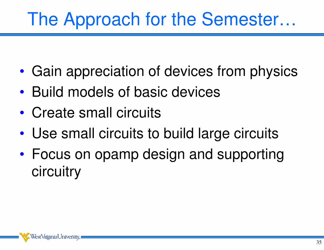
The Approach for the Semester…
• Gain appreciation of devices from physics
• Build models of basic devices
• Create small circuits
• Use small circuits to build large circuits
• Focus on opamp design and supporting circuitry