Embed Size (px)
Citation preview
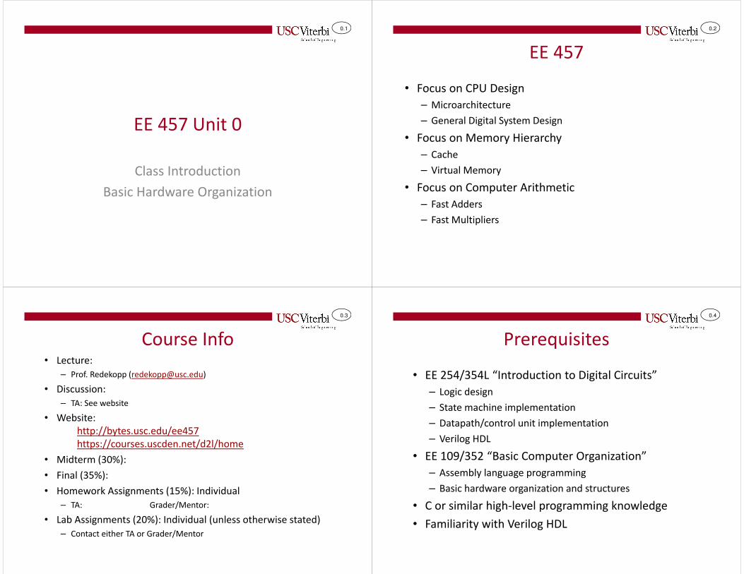
0.1
EE 457 Unit 0
Class Introduction
Basic Hardware Organization
0.2
EE 457
• Focus on CPU Design
– Microarchitecture
– General Digital System Design
• Focus on Memory Hierarchy
– Cache
– Virtual Memory
• Focus on Computer Arithmetic
– Fast Adders
– Fast Multipliers
0.3
Course Info• Lecture:
– Prof. Redekopp ([email protected])
• Discussion:
– TA: See website
• Website:
http://bytes.usc.edu/ee457
https://courses.uscden.net/d2l/home
• Midterm (30%):
• Final (35%):
• Homework Assignments (15%): Individual
– TA: Grader/Mentor:
• Lab Assignments (20%): Individual (unless otherwise stated)
– Contact either TA or Grader/Mentor
0.4
Prerequisites
• EE 254/354L “Introduction to Digital Circuits”
– Logic design
– State machine implementation
– Datapath/control unit implementation
– Verilog HDL
• EE 109/352 “Basic Computer Organization”
– Assembly language programming
– Basic hardware organization and structures
• C or similar high-level programming knowledge
• Familiarity with Verilog HDL
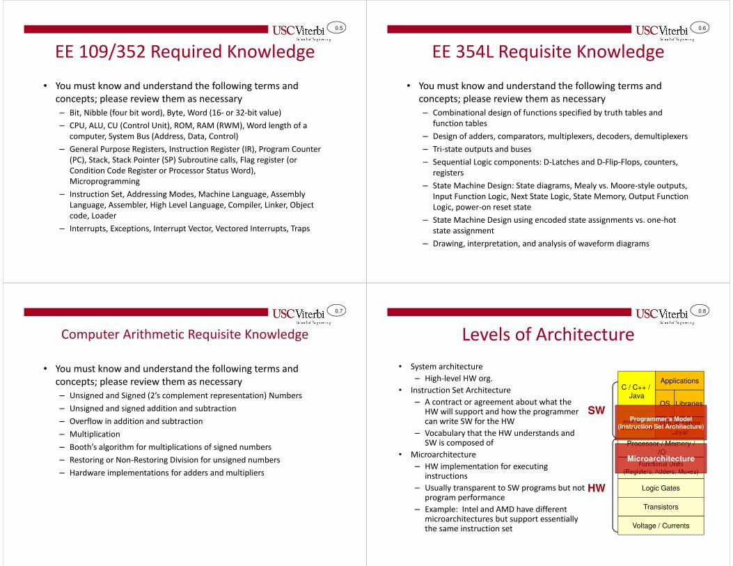
0.5
EE 109/352 Required Knowledge
• You must know and understand the following terms and
concepts; please review them as necessary
– Bit, Nibble (four bit word), Byte, Word (16- or 32-bit value)
– CPU, ALU, CU (Control Unit), ROM, RAM (RWM), Word length of a
computer, System Bus (Address, Data, Control)
– General Purpose Registers, Instruction Register (IR), Program Counter
(PC), Stack, Stack Pointer (SP) Subroutine calls, Flag register (or
Condition Code Register or Processor Status Word),
Microprogramming
– Instruction Set, Addressing Modes, Machine Language, Assembly
Language, Assembler, High Level Language, Compiler, Linker, Object
code, Loader
– Interrupts, Exceptions, Interrupt Vector, Vectored Interrupts, Traps
0.6
EE 354L Requisite Knowledge
• You must know and understand the following terms and
concepts; please review them as necessary
– Combinational design of functions specified by truth tables and
function tables
– Design of adders, comparators, multiplexers, decoders, demultiplexers
– Tri-state outputs and buses
– Sequential Logic components: D-Latches and D-Flip-Flops, counters,
registers
– State Machine Design: State diagrams, Mealy vs. Moore-style outputs,
Input Function Logic, Next State Logic, State Memory, Output Function
Logic, power-on reset state
– State Machine Design using encoded state assignments vs. one-hot
state assignment
– Drawing, interpretation, and analysis of waveform diagrams
0.7
Computer Arithmetic Requisite Knowledge
• You must know and understand the following terms and
concepts; please review them as necessary
– Unsigned and Signed (2’s complement representation) Numbers
– Unsigned and signed addition and subtraction
– Overflow in addition and subtraction
– Multiplication
– Booth’s algorithm for multiplications of signed numbers
– Restoring or Non-Restoring Division for unsigned numbers
– Hardware implementations for adders and multipliers
0.8
Levels of Architecture
• System architecture
– High-level HW org.
• Instruction Set Architecture
– A contract or agreement about what the HW will support and how the programmer can write SW for the HW
– Vocabulary that the HW understands and SW is composed of
• Microarchitecture
– HW implementation for executing instructions
– Usually transparent to SW programs but not program performance
– Example: Intel and AMD have different microarchitectures but support essentially the same instruction set
C / C++ /
Java
Logic Gates
Transistors
HW
SW
Voltage / Currents
Applications
LibrariesOS
Processor / Memory /
I/O
Functional Units(Registers, Adders, Muxes)
Assembly /
Machine Code
Microarchitecture
Virtualization
Layer
Programmer’s Model(Instruction Set Architecture)

0.9
Why is Architecture Important
• Enabling ever more capable computers
• Different systems require different architectures– PC’s
– Servers
– Embedded Systems• Simple control devices like ATM’s, toys, appliances
• Media systems like game consoles and MP3 players
• Robotics
0.10
Digital System Spectrum
• Key idea: Any “algorithm” can be implemented in HW or SW or some mixture of both
• A digital systems can be located anywhere in a spectrum of:
– ALL HW: (a.k.a. Application-Specific IC’s)
– ALL SW: An embedded computer system
• Advantages of application specific HW
– Faster, less power
• Advantages of an embedded computer system (i.e. general purpose HW for executing SW)
– Reprogrammable (i.e. make a mistake, fix it)
– Less expensive than a dedicated hardware system (single computer system can be used for multiple designs)
• MP3 Player: System-on-Chip (SoC) approach
– Some dedicated HW for intensive MP3 decoding operations
– Programmable processor for UI & other simple tasks
Co
mp
uti
ng
Syste
m
Sp
ectr
um
Application Specific Hardware
(no software)
General Purpose HW w/ Software
Fle
xib
ilit
y, D
es
ign
Tim
e
Pe
rfo
rma
nc
e
Co
st
http://d2rormqr1qwzpz.cloudfront.net/photos/2014/01/01/56914-moto_x.jpg
0.11
Computer Components
• Processor
– Executes the program and performs all the operations
• Main Memory
– Stores data and program(instructions)
– Different forms:
• RAM = read and write but volatile (lose values when power off)
• ROM = read-only but non-volatile (maintains values when power off)
– Significantly slower than the processor speeds
• Input / Output Devices
– Generate and consume data from the system
– MUCH, MUCH slower than the processor
Arithmetic + Logic + Control Circuitry
Program(Instructions)
Data(Operands)
Output
Devices
Input
Devices
Data
Software Program
Memory (RAM)
Processor
Combine 2c. Flour
Mix in 3 eggsInstructions
DataProcessor
(Reads instructions, operates on data)
Disk Drive
0.12
ARCHITECTURE OVERVIEW
Drivers and Trends
0.13
Architecture Issues
• Fundamentally, architecture is all about the different
ways of answering the question:
“What do we do with the ever-increasing number of
transistors available to us”
• Goal of a computer architect is to take increasing
transistor budgets of a chip (i.e. Moore’s Law) and
produce an equivalent increase in computational
ability
0.14
Moore’s Law, Computer Architecture & Real-
Estate Planning
• Moore’s Law = Number of
transistors able to be
fabricated on a chip grows
exponentially with time
• Computer architects decide,
“What should we do with all
of this capability?”
• Similarly real-estate
developers ask, “How do we
make best use of the land
area given to us?”USC University Park Development Master Plan
http://re.usc.edu/docs/University%20Park%20Development%20Project.pdf
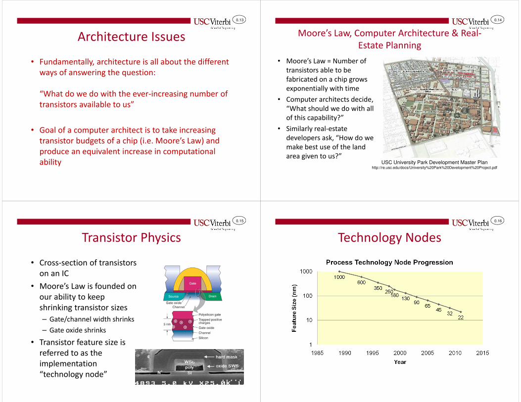
0.15
Transistor Physics
• Cross-section of transistors
on an IC
• Moore’s Law is founded on
our ability to keep
shrinking transistor sizes
– Gate/channel width shrinks
– Gate oxide shrinks
• Transistor feature size is
referred to as the
implementation
“technology node”
0.16
Technology Nodes
0.17
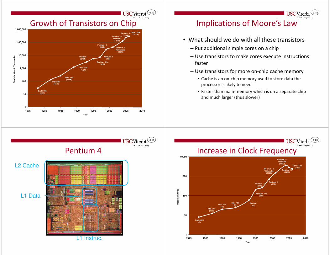
Growth of Transistors on Chip
1
10
100
1,000
10,000
100,000
1,000,000
1975 1980 1985 1990 1995 2000 2005 2010
Tra
nis
tor
Co
un
t (T
ho
usan
ds)
Year
Intel '486(1.2M)
Pentium(3.1M)
Pentium Pro(5.5M)
Pentium 3(28M) Pentium 4
Northwood(42M)
Pentium 2(7M)
Intel '386(275K)
Intel '286(134K)
Intel 8086(29K)
Pentium 4 Prescott(125M)
Pentium D(230M)
Core 2 Duo(291M)
0.18
Implications of Moore’s Law
• What should we do with all these transistors
– Put additional simple cores on a chip
– Use transistors to make cores execute instructions
faster
– Use transistors for more on-chip cache memory
• Cache is an on-chip memory used to store data the
processor is likely to need
• Faster than main-memory which is on a separate chip
and much larger (thus slower)
0.19
Pentium 4
L2 Cache
L1 Data
L1 Instruc.
0.20
Increase in Clock Frequency
1
10
100
1000
10000
1975 1980 1985 1990 1995 2000 2005 2010
Fre
qu
en
cy (
MH
z)
Year
Intel '486(25)
Pentium(60)
Pentium Pro(200)
Pentium 3(700)
Pentium 4 Willamette
(1500)
Pentium 2(266)
Intel '386(20)
Intel '286(12.5)
Intel 8086(8)
Pentium 4 Prescott (3600)
Pentium D (2800)
Core 2 Duo(2400)
0.21
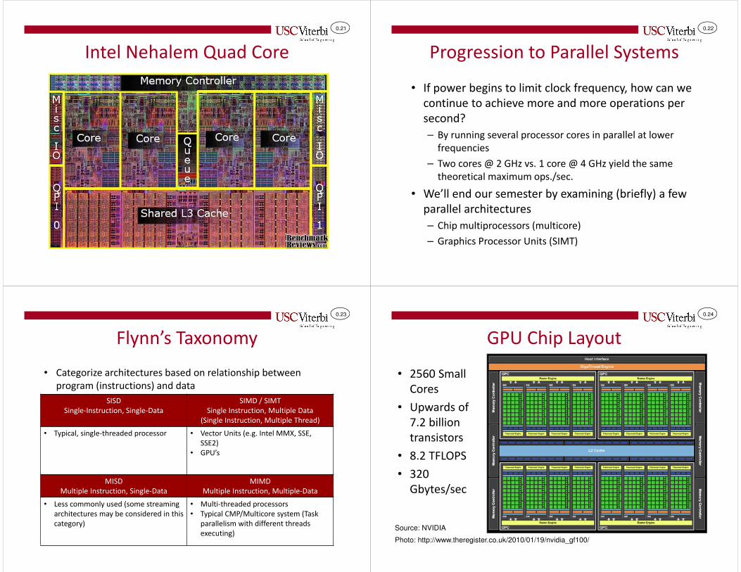
Intel Nehalem Quad Core
0.22
Progression to Parallel Systems
• If power begins to limit clock frequency, how can we
continue to achieve more and more operations per
second?
– By running several processor cores in parallel at lower
frequencies
– Two cores @ 2 GHz vs. 1 core @ 4 GHz yield the same
theoretical maximum ops./sec.
• We’ll end our semester by examining (briefly) a few
parallel architectures
– Chip multiprocessors (multicore)
– Graphics Processor Units (SIMT)
0.23
Flynn’s Taxonomy
• Categorize architectures based on relationship between
program (instructions) and data
SISD
Single-Instruction, Single-Data
SIMD / SIMT
Single Instruction, Multiple Data
(Single Instruction, Multiple Thread)
• Typical, single-threaded processor • Vector Units (e.g. Intel MMX, SSE,
SSE2)
• GPU’s
MISD
Multiple Instruction, Single-Data
MIMD
Multiple Instruction, Multiple-Data
• Less commonly used (some streaming
architectures may be considered in this
category)
• Multi-threaded processors
• Typical CMP/Multicore system (Task
parallelism with different threads
executing)
0.24
GPU Chip Layout
• 2560 Small
Cores
• Upwards of
7.2 billion
transistors
• 8.2 TFLOPS
• 320
Gbytes/sec
Photo: http://www.theregister.co.uk/2010/01/19/nvidia_gf100/
Source: NVIDIA
0.25
Intel Haswell Quad Core
0.26
COMPUTER SYSTEM TOUR
In case you need a review…Look these over on your own
0.27
Computer Systems Tour
• How does a SW program get mapped and executed on a computer
• What components make a computer system and what are their functions
• How does the architecture affect performance
C / C++ / Java
Logic Gates
Transistors
HW
SW
Voltage / Currents
Assembly /
Machine Code
Applications
LibrariesOS
Processor / Memory / I/O
Functional Units
(Registers, Adders, Muxes)
Start Here
0.28
Software Process
1110 0010 0101 10010110 1011 0000 11000100 1101 0111 11111010 1100 0010 10110001 0110 0011 1000
MOVE.W X,D0CMPI.W #0,D0BLE SKIPADD Y,D0SUB Z,D0
SKIP MUL …
Software Program
High Level Language
Description
Assembly (.asm/.s files)
Executable Binary Image
if (x > 0)x = x + y - z;
a = b*x;
MOVE.L X,D0CMPI #0,D0BLE SKIPADD Y,D0SUB Z,D0
SKIP MUL …
1110 0010 0101 10010110 1011 0000 11000100 1101 0111 11111010 1100 0010 10110001 0110 0011 1000
.c/.cpp files1110 0010 0101 10010110 1011 0000 11000100 1101 0111 11111010 1100 0010 10110001 0110 0011 1000
Object/Machine Code(.o files)
Compiler Assembler
LinkerLoader / OS
Program Executing
In EE 357 you will be able to perform all the tasks of the compiler…
A “compiler”(i.e. gcc, VisualC++,
etc.) includes the assembler & linker
0.29
Compiler Process
• A compiler such as ‘gcc’ performs 3 tasks:
– Compiler
• Converts HLL (high-level language) files to assembly
– Assembler
• Converts assembly to object (machine) code
– Static Linker
• Links multiple object files into a single executable resolving references between code in the separate files
– Output of a compiler is a binary image that can be loaded into memory and then executed.
• Loader/Dynamic Linker
– Loads the executable image into memory and resolves dynamic calls (to OS subroutines, libraries, etc.)
0.30
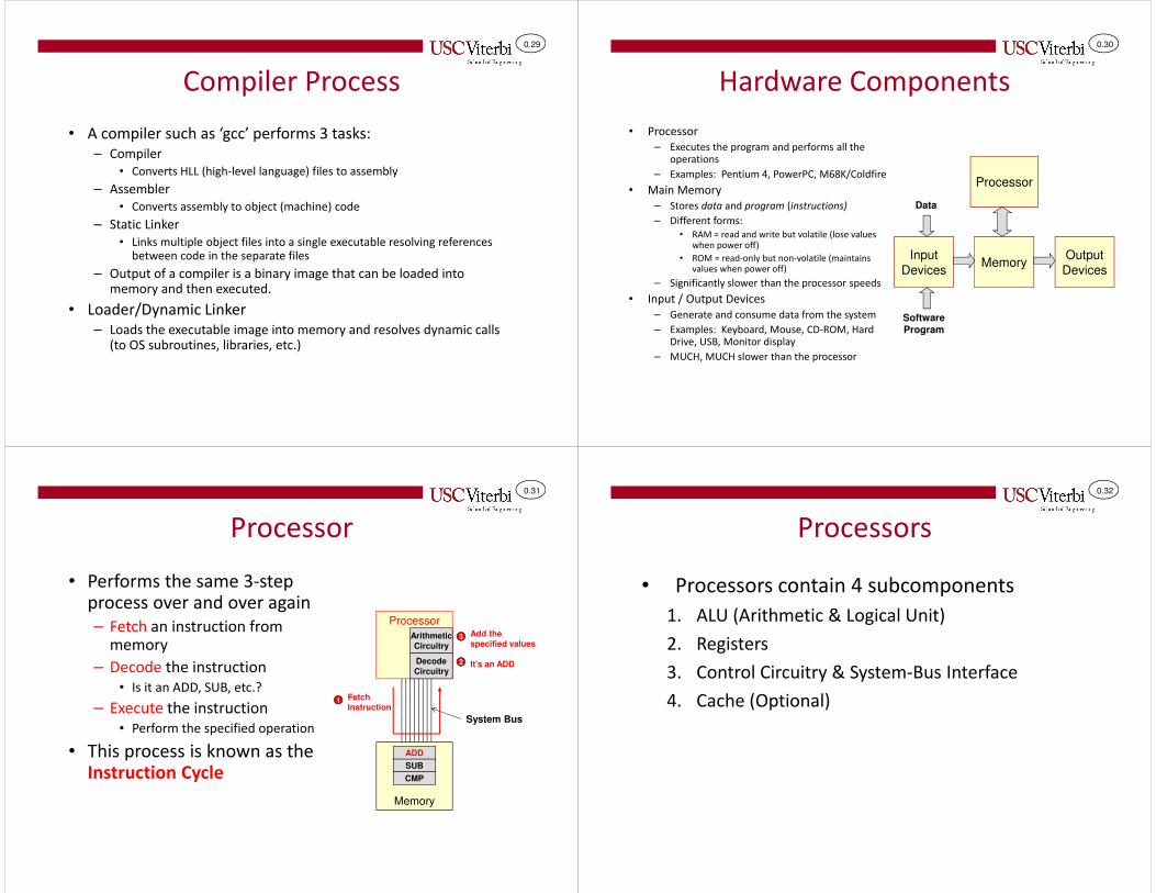
Hardware Components
• Processor
– Executes the program and performs all the operations
– Examples: Pentium 4, PowerPC, M68K/Coldfire
• Main Memory
– Stores data and program (instructions)
– Different forms:
• RAM = read and write but volatile (lose values when power off)
• ROM = read-only but non-volatile (maintains values when power off)
– Significantly slower than the processor speeds
• Input / Output Devices
– Generate and consume data from the system
– Examples: Keyboard, Mouse, CD-ROM, Hard Drive, USB, Monitor display
– MUCH, MUCH slower than the processor
Processor
MemoryOutput
Devices
Input
Devices
Software Program
Data
0.31
Processor
• Performs the same 3-step process over and over again
– Fetch an instruction from memory
– Decode the instruction
• Is it an ADD, SUB, etc.?
– Execute the instruction
• Perform the specified operation
• This process is known as the Instruction Cycle
Processor
Memory
ADD
SUB
CMP
ArithmeticCircuitry
DecodeCircuitry
1 Fetch Instruction
It’s an ADD
Add the specified values
2
3
System Bus
0.32
Processors
• Processors contain 4 subcomponents
1. ALU (Arithmetic & Logical Unit)
2. Registers
3. Control Circuitry & System-Bus Interface
4. Cache (Optional)

0.33
ALU
• Performs arithmetic and logical operations
• 2 inputs and 1 output value
• Control inputs to select operation (ADD, SUB, AND, OR…)
ALU
Control
Processor
0.34
Registers
• Provide temporary storage for data
• 2 categories of registers
– General Purpose Registers (GPR’s)
• for program data
• can be used by programmer as desired
• given names (e.g. D0-D7)
– Special Purpose Registers
• for internal processor operation (not for program data)
ALU
Control
Processor
MIPS Core
$0 - $31
32-bits
GPR’s
Special Purpose Registers
PC:
IR:
HI:
LO:
0.35
Registers
• GPR’s– Faster to access than main
memory
– Keep data you are working with in registers to speed up execution
• Special Purpose Reg’s.– Hold specific information that
the processor needs to operate correctly
– PC (Program Counter)• Pointer to (address of)
instruction in memory that will be executed next
– IR (Instruction Register)• Stores the instruction while it
is being executed
– SR (Status Register)• Stores status/control info
ALU
Control
Processor
MIPS Core
$0 - $31
32-bits
GPR’s
Special Purpose Registers
PC:
IR:
HI:
LO:
0.36
Control Circuitry
• Decodes each
instruction
• Selects appropriate
registers to use
• Selects ALU
operation
• And more…
Registers
ALU
Control
Control Circuitry
Processor
$0
…
$1
PC
IR
0.37
System Bus Interface
• System bus is the means of communication between the processor and other devices
– Address
• Specifies location of instruction or data
– Data
– ControlAddress
Data
Control
Registers
ALU
Control
Control Circuitry
Processor
$0
…
$1
PC
IR
0.38
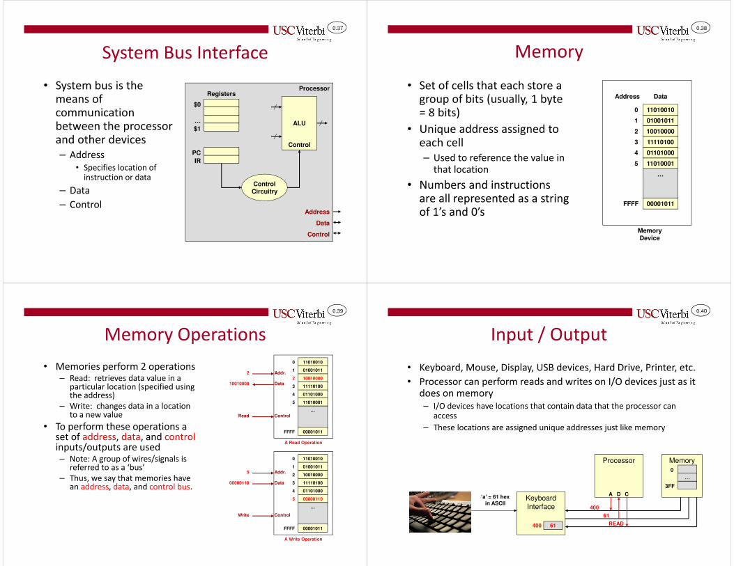
Memory
• Set of cells that each store a group of bits (usually, 1 byte = 8 bits)
• Unique address assigned to each cell
– Used to reference the value in that location
• Numbers and instructions are all represented as a string of 1’s and 0’s
11010010
01001011
10010000
11110100
01101000
11010001
…
00001011
0
1
2
3
4
5
FFFF
Address Data
Memory Device
0.39
Memory Operations
• Memories perform 2 operations– Read: retrieves data value in a
particular location (specified using the address)
– Write: changes data in a location to a new value
• To perform these operations a set of address, data, and controlinputs/outputs are used– Note: A group of wires/signals is
referred to as a ‘bus’
– Thus, we say that memories have an address, data, and control bus.
11010010
01001011
10010000
11110100
01101000
11010001
…
00001011
0
1
2
3
4
5
FFFF
11010010
01001011
10010000
11110100
01101000
00000110
…
00001011
0
1
2
3
4
5
FFFF
2
10010000
Read
Addr.
Data
Control
Addr.
Data
Control
5
00000110
Write
A Write Operation
A Read Operation
0.40
Input / Output
• Keyboard, Mouse, Display, USB devices, Hard Drive, Printer, etc.
• Processor can perform reads and writes on I/O devices just as it does on memory
– I/O devices have locations that contain data that the processor can access
– These locations are assigned unique addresses just like memory
Keyboard
Interface
‘a’ = 61 hex in ASCII
61400
Processor Memory
A D C
400
61
READ
…
0
3FF
0.41
Input / Output
• Writing a value to the video adapter can set a pixel on the screen
Video
InterfaceFE may signify a
white dot at a particular
location
…
800
Processor Memory
A D C
800
FE
WRITE
…
0
3FF
FE
01
Keyboard
Interface
61400
0.42
Computer Organization Issues
• Components run at different speeds– Processor can perform operations very quickly (~ 1 ns)
– Memory is much slower (~ 50 ns) due to how it is constructed & its shear size [i.e. it must select/look-up 1 location from millions]
• Speed is usually inversely proportional to size (i.e. larger memory => slower)
– I/O devices are much slower• Hard Drive (~ 1 ms)
– Intra-chip signals (signals w/in the same chip) run much faster than inter-chip signals
• Design HW and allocate HW resources to accommodate these inherent speed differences


![[Shinobi] Bleach 457](https://img.pdfslide.us/doc/110x75/568c0f8d1a28ab955a9484ea/shinobi-bleach-457.jpg)