Embed Size (px)
Citation preview

Atomistic Simulation of Nanodevices(Invited Paper)
Mathieu Luisier∗, Reto Rhyner†, Aron Szabo∗, and Andreas Pedersen∗∗Integrated Systems Laboratory, ETH Zurich, CH-8092 Zurich, Switzerland
† Synopsys Switzerland LLC, CH-8050 Zurich, Switzerland
Abstract—As the dimensions of electronic devices, especiallytransistors, are getting smaller and smaller, novel modelingapproaches must be developed to reveal the physics and predictthe performance of not-yet-fabricated ultra-scaled components.In this paper the basic requirements to simulate nanoscale devicesare first reviewed before introducing a hierarchical quantumtransport approach going from empirical to ab-initio models. It isillustrated with three examples, a Si nanowire transistor treatedwithin nearest-neighbor tight-binding (TB), a 2-D logic switchbased on transition metal dichalcogenides and investigated withan hybrid scheme combining the advantages of TB and density-functional theory, and finally a silver nano-filament explored atthe first-principles level. The importance of dissipative effectssuch as electron-phonon scattering is discussed in all applications.
I. INTRODUCTION
At the heart of laptops, tablets, or cell phones sit inte-grated circuits, lithium ion batteries, and memory cells thatensure the proper functionality of these modern electronicdevices. By further diving into these hardware components,one may find integrated circuits relying on nanoscale logicswitches, in most cases FinFETs, cathodes and anodes withhigh power and energy densities due to the presence of porousnano-particles, or ultra-short metal-insulator-metal junctionsenabling a non-volatile storage of digital information. Besidesreduced dimensions the mentioned nanostructures share otherpeculiar features: their active region is usually made of acountable number of atoms and their behavior is stronglyinfluenced by quantum mechanical effects. As a consequenceand contrary to the recent past, standard recipes, intuition, andextrapolation from previous generations might not be sufficientanymore to design novel nanoelectronic devices with enhancedperformance and higher complexity.
The experimental work can be greatly enhanced by addinga modeling activity to support the initial design process andshed light on the mechanisms that determine the properties offabricated samples. If a suitable technology computer aideddesign tool (TCAD) is available, less trial-and-error iterationsare needed before a successful prototype is demonstrated.This is particularly true at the nanoscale, where the costsof production are consequent and the manufacturing cyclesrelatively long. To be useful to a nano-device engineer, aTCAD tool should provide measurable data that can be directlycompared to experiments and give access to internal quantitieswhose knowledge is essential to understand the behavior of theconsidered systems. This includes for example insights into the
underlying atomic structure, the magnitude of the electron/holecurrents induced by the application of external voltages, thecarrier trajectories inside the active region, or the distributionof the lattice temperature. The right physical models shouldbe implemented in the chosen TCAD framework to make suchdetailed analyses possible.
Since (semi-)classical theories such as drift-diffusion or theBoltzmann Transport Equation fails at incorporating the atom-istic granularity of simulation domains as well as quantummechanical effects, they should be replaced by more advancedtechniques that offer the desired level of accuracy. At thenanometer scale a direct solution of the Schrodinger equationimposes itself to account for atomistic quantum transportphenomena. This can be achieved with the well-establishedNon-equilibrium Green’s Function (NEGF) formalism, whichwill be briefly summarized here in Section II and illustratedwith three different examples in Section III.
II. SIMULATION APPROACH
To determine the transport properties of nanoscale devices,open boundary conditions (OBCs) should be introduced intothe Schrodinger equation in order to enable the injection offermions and bosons into the simulated region. If this is donein the framework of NEGF [1] the generic equations forfermions are the following
(
𝐸 −𝐻(𝑘)− Σ𝑅(𝑘,𝐸)) ⋅𝐺𝑅(𝑘,𝐸) = 𝐼 (1)
𝐺≷(𝑘,𝐸) = 𝐺𝑅(𝑘,𝐸) ⋅ Σ≷(𝑘,𝐸) ⋅𝐺𝐴(𝑘,𝐸), (2)
Σ≷,𝑅(𝐸, 𝑘) = Σ≷,𝑅𝐵(𝐸, 𝑘) + Σ≷,𝑅𝑆(𝐸, 𝑘). (3)
Similar equations can be derived for phonons [2] and photons.In Eqs. (1) and (2), the unknowns are the retarded/advanced𝐺𝑅/𝐴(𝑘,𝐸) and lesser/greater 𝐺≷(𝑘,𝐸) Green’s functionsat energy 𝐸 and momentum 𝑘. They are full matrices ofsize 𝑁𝐴 × 𝑁𝐵 where 𝑁𝐴 is the number of discretizationpoints in the simulation domain and 𝑁𝐵 the number of basiscomponents describing each of them. The momentum (𝑘)dependence arises from the modeling of the directions thatare assumed periodic. The diagonal matrix 𝐸 contains theelectron/hole energy, the usually block tri-diagonal matrix𝐻(𝑘) is the device Hamiltonian, while the open boundaryconditions are cast into the self-energy matrices Σ𝑅,≷𝐵(𝑘,𝐸)and the scattering mechanisms into Σ𝑅,≷𝑆(𝑘,𝐸). The keyingredients in Eqs. (1) and (2) are the Hamiltonian 𝐻(𝑘) thatcan be expressed in various atomistic basis sets, as will bediscussed in Section III, and the choice of the interactionsthat are integrated into Σ≷,𝑅𝑆(𝑘,𝐸).978-1-5090-0818-6/16/$31.00 c⃝ 2016 IEEE
Simulation of Semiconductor Processes and Devices 2016Edited by E. Bär, J. Lorenz, and P. Pichler
281

−4
−2
0
2
4
6E
(eV)
L Γ X Γelectrons holes
1600
1200
800
400
mob
ility
(cm
2 /Vs
)
electronsholesexp.
(a)
(b) (c)10
110
210
3101
102
103
104
Temperature (K)
Ther
mal
Con
duct
ivity
(W/m
K)
ExperimentSimulation
Fig. 1. (a) Si bulk bandstructure as computed with the nearest-neighbor tight-binding parameters of Ref. [9]. (b) Electron and hole mobility of bulk Si. Thesquare and triangle refer to calculations performed with the “dR/dL” method [10] in the presence of electron-phonon scattering, the stars to experimental data.(c) Lattice thermal conductivity of bulk Si as obtained from phonon quantum transport simulations including anharmonic phonon phonon scattering (red linewith symbols) and from experiments (blue line) [11].
A. Ballistic Transport
The NEGF formalism is best-suited for transport situationswhere scattering should be accounted for. In the ballistic limit,Eq. (1) can be reformulated into a Wave Function problemknown as Quantum Transmitting Boundary Method (QTBM)that produces exactly the same results as NEGF, but fastersince it takes the form of a sparse linear system of equations“Ax=b” [3], [4]
(
𝐸 −𝐻(𝑘)− Σ𝑅𝐵(𝐸, 𝑘))
︸ ︷︷ ︸
𝐴
⋅𝐶(𝐸, 𝑘)︸ ︷︷ ︸
𝑥
= 𝐼𝑛𝑗(𝐸, 𝑘)︸ ︷︷ ︸
𝑏
. (4)
In Eq. (4) the injection vector 𝐼𝑛𝑗(𝐸, 𝑘) is also part ofthe OBCs and the unknowns are the expansion coefficients𝐶(𝐸, 𝑘). Direct sparse linear solvers, sequential or parallel,can be utilized to handle the “Ax=b” system in Eq. (4).
B. Dissipative Transport: Electron-Phonon Scattering
As soon as scattering is turned on, the NEGF formalismshould be used because it lends itself naturally to this kind ofphysical problems. In case of electron-phonon scattering, thelesser scattering self-energy can be formulated as
Σ<𝑆(𝑘,𝐸) ∝∑
𝜔
∫
𝑑𝑞
2𝜋𝑉 (𝜔, 𝑞)
∇𝐻(
𝑛𝜔𝐺<(𝑘 − 𝑞, 𝐸 + ℏ𝜔)+
(𝑛𝜔 + 1)𝐺<(𝑘 − 𝑞, 𝐸 − ℏ𝜔))∇𝐻 (5)
The expression for Σ>𝑆(𝑘,𝐸) and Σ𝑅𝑆(𝑘,𝐸) can be foundin Ref. [5]. The phonon frequencies 𝜔 and modes 𝜇 enter thisequation, either directly or through the form factor 𝑉 (𝜔, 𝑞)that is a function of both of them and through the phonondistribution function 𝑛𝜔 (Bose-Einstein). Here, it is assumedthat the phonon population remains in equilibrium with itsenvironment, but it can be driven out-of-equilibrium by solvingthe corresponding phonon Green’s functions and phonon-electron scattering self-energy [6]. This gives rise to self-heating effects and the formation of local hot spots.
Since Σ<𝑆(𝑘,𝐸) in Eq. (5) depends on the Green’s Func-tion and vice-versa, these quantities must be iteratively com-puted in the so-called self-consistent Born approximation tillconvergence is reached. It is very convenient to solve Eqs. (1)and (2) with a recursive Green’s Function (RGF) algorithm[7]. Finally, regardless of the transport regime, ballistic ordissipative, Eqs. (1) and (2) or Eq. (4) must be evaluatedat each possible 𝐸 and 𝑘 to obtain the current and chargedensity of the considered devices. The charge is then self-consistently coupled to the electrostatic potential throughPoisson’s equation expressed on a finite element grid.
III. RESULTS
Three applications have been selected to highlight the bene-fits of atomistic quantum transport simulations. Each of themrelies on a different device configuration (Si nanowire, 2-Dsemiconductor, Ag nano-filament) and on a different modelingapproach (tight-binding, Wannier functions, ab-initio basis).
A. Tight-Binding
Empirical nearest-neighbor tight-binding models, as pro-posed by Slater and Koster [8], allow to account for fullbandstructures at low computational costs, while still capturingevery single atom constituting the investigated device struc-tures. An example with bulk Si is given in Fig. 1(a), wherethe 𝑠𝑝3𝑑5𝑠∗ parameterization of Ref. [9] has been used. Byturning on electron-phonon scattering, the bulk electron andhole mobility of Si can be obtained, as shown in Fig. 1(b). Thisrequires either solving the linearized Boltzmann TransportEquation or applying the “dR/dL” method and extracting theresistance of samples with various lengths [10]. The results ofboth approaches agree very well with available experimentaldata, especially for electrons. However, with the chosen pa-rameters the hole mobility tends to be overestimated by about100 cm2/Vs, which remains acceptable in most applications.
The counterpart of tight-binding for phonons is the so-calledvalence-force-field (VFF) method that produces the oscillationfrequencies and amplitudes of a given crystal based on alimited number of input parameters, typically between 2 and
282 Simulation of Semiconductor Processes and Devices 2016Edited by E. Bär, J. Lorenz, and P. Pichler
0 0.1 0.2 0.3 0.4 0.5 0.6
10−1
100
101
102
103
Vgs
(V)
I d (μA
/μm
)
0
1000
2000
3000
4000
I(μ
A/μ
m)
Ballistice−ph (eq.)e−ph (non−eq.)
dCR1
CR2
diameter
tox
y
xz
Source
DrainLg
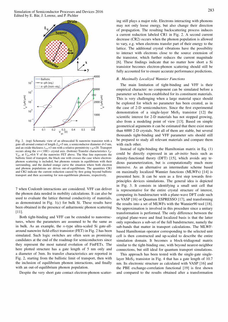
Fig. 2. (top) Schematic view of an ultrascaled Si nanowire transistor with agate-all-around contact of length 𝐿𝑔=5 nm, a semiconductor diameter 𝑑=3 nm,and an oxide thickness 𝑡𝑜𝑥=3 nm with a relative permittivity 𝜖𝑅=20. Transportoccurs along the 𝑥=<100> crystal axis. (bottom) Transfer characteristics 𝐼𝑑-𝑉𝑔𝑠 at 𝑉𝑑𝑠=0.6 V of the nanowire FET above. The blue line represents theballistic limit of transport, the black one with crosses the case where electron-phonon scattering is included, but phonons remain in equilibrium with theirsurrounding, and the dashed orange curve the situation where both electronand phonon populations are driven out-of-equilibrium. The quantities CR1and CR2 indicate the current reduction caused by first going beyond ballistictransport and then accounting for non-equilibrium phonons, respectively.
7 when Coulomb interactions are considered. VFF can deliverthe phonon data needed in mobility calculations. It can also beused to evaluate the lattice thermal conductivity of materials,as demonstrated in Fig. 1(c) for bulk Si. These results havebeen obtained in the presence of anharmonic phonon scattering[11].
Both tight-binding and VFF can be extended to nanostruc-tures, where the parameters are assumed to be the same asin bulk. As an example, the 𝑛-type ultra-scaled Si gate-all-around nanowire field-effect transistor (FET) in Fig. 2 has beensimulated. Such logic switches are often seen as promisingcandidates at the end of the roadmap for semiconductors sincethey represent the most natural evolution of FinFETs. Thehere plotted structure has a gate length of 5 nm only anda diameter of 3nm. Its transfer characteristics are reported inFig. 2, starting from the ballistic limit of transport, then withthe inclusion of equilibrium phonon interactions, and finallywith an out-of-equilibrium phonon population.
Despite the very short gate contact electron-phonon scatter-
ing still plays a major role. Electrons interacting with phononsmay not only loose energy, but also change their directionof propagation. The resulting backscattering process inducesa current reduction labeled CR1 in Fig. 2. A second currentdecrease (CR2) occurs when the phonon population is allowedto vary, e.g. when electrons transfer part of their energy to thelattice. The additional crystal vibrations have the possibilityto interact with electrons close to the source extension ofthe transistor, which further reduces the current magnitude[6]. These findings indicate that no matter how short a Sitransistor becomes electron-phonon scattering should still befully accounted for to ensure accurate performance predictions.
B. Maximally Localized Wannier Functions
The main limitation of tight-binding and VFF is theirempirical character: no component can be simulated before aparameter set has been established for its constituent materials.This is very challenging when a large material space shouldbe explored for which no parameter has been created, as inthe case of 2-D semiconductors. Since the first experimentaldemonstration of a single-layer MoS2 transistor [12] thescientific interest for 2-D materials has not stopped growing,also from a modeling point of view [13]. Based on simplegeometrical arguments it can be estimated that there exist morethan 6000 2-D crystals. Not all of them are stable, but severalthousands tight-binding and VFF parameter sets should stillbe prepared to study all relevant materials and compare themwith each other.
Instead of tight-binding the Hamiltonian matrix in Eq. (1)could be directly expressed in an ab-initio basis such asdensity-functional theory (DFT) [15], which avoids any te-dious parameterization, but is computationally much moreintensive. As an alternative an intermediate scheme basedon maximally localized Wannier functions (MLWFs) [14] ispresented here. It can be seen as a first step towards first-principles devices simulations. The general idea is depictedin Fig. 3. It consists in identifying a small unit cell thatis representative for the entire crystal structure of interest,computing its bandstructure with a plane-wave DFT code suchas VASP [16] or Quantum ESPRESSO [17], and transformingthe results into a set of MLWFs with the Wannier90 tool [18].No approximation is involved in this procedure since a unitarytransformation is performed. The only difference between theoriginal plane-wave and final localized basis is that the latteronly reproduces a sub-set of the full bandstructure, namely thesub-bands that matter in transport calculations. The MLWF-based Hamiltonian operator corresponding to the selected unitcell is then constructed and up-scaled to describe the entiresimulation domain. It becomes a block-tridiagonal matrixsimilar to the tight-binding one, with beyond nearest-neighborconnections, but still ideal for quantum transport simulations.
This approach has been tested with the single-gate single-layer MoS2 transistor in Fig. 4 that has a gate length of 10.7nm. Its electronic structure as calculated with VASP [16] andthe PBE exchange-correlation functional [19] is first shownand compared to the results obtained after a transformation
Simulation of Semiconductor Processes and Devices 2016Edited by E. Bär, J. Lorenz, and P. Pichler
283

Ab-ini�o electronic structure calcula�on
Conversion to maximally-localized Wannier func�on basis
Quantum transport with �ght-binding-like Hamiltonian
Fig. 3. Coupling scheme between density-functional theory, e.g. VASP [16] or Quantum ESPRESSO [17] and quantum transport calculations through thetransformation of the produced plane-wave outputs into a set of maximally localized Wannier functions. The Wannier90 tool is used for that purpose [18].This process results in a tight-binding-like Hamiltonian matrix with beyond nearest-neighbor connections.
Lg
Single-layerMoS2
K Γ M
Elec
tron
Ene
rgy
(eV)
DFTMLWFsE g
K 0
10
20
30
40
50
60
Γ K M Γ
Phon
on E
nerg
y (m
eV)
x
y
−4
−3
−2
−1
0
1
Fig. 4. (left) Schematic view of a single-gate transistor with a monolayer of MoS2 as active region, 𝐿𝑔=10.7 nm, and an equivalent oxide thickness EOT=0.58nm. (center) Comparison between the bandstructure of single-layer MoS2 as calculated with a plane-wave DFT tool [16] and PBE functional [19] (solid bluelines) and with a quantum transport solver after a unitary transformation into MLWFs (red dots). (right) Phonon bandstructure of single-layer MoS2 based ondensity-functional perturbation theory (DFPT) [21] .
0 0.2 0.4 0.610
−3
10−2
10−1
100
101
102
103
Vgs
(V)
I d (μA
/μm
)
Vds
=0.05 V
Vds
=0.68 V
0
500
1000
I d (μA
/μm
)(a)
0 0.2 0.4 0.610
−3
10−2
10−1
100
101
102
103
Vgs
(V)
Vds
=0.05 V
Vds
=0.68 V
0
500
1000
I d (μA
/μm
)
x (nm)
Ener
gy (e
V)
CB Edge
phonon emission
0 10 20 30−0.6
−0.55
−0.5
−0.45
−0.4
40
(b)(c)
Fig. 5. (a) Ballistic transfer characteristics of the single-layer MoS2 transistor in Fig. 4 at 𝑉𝑑𝑠=0.05 V (solid blue line) and 0.68 V (dashed red line). (b)Same as (a), but in the presence of electron-phonon scattering. (c) Spectral current of the same transistor as before showing the band coupling induced byphonon emission. Red indicates high current concentrations, green no current, the dashed blue line refers to the conduction band edge.
into a MLWF basis with five 𝑑-like (three 𝑝-like) orbitalsper Mo (S) atom. A very good agreement can be observed,although small discrepancies originating from the truncationof long-range interactions are present.
The ballistic transfer characteristics 𝐼𝑑-𝑉𝑔𝑠 of this device at𝑉𝑑𝑠=0.05 and 0.68 V are presented in Fig. 5(a). A negativedifferential resistance (NDR) behavior can be noticed, i.e. the
current at high 𝑉𝑑𝑠 is smaller than at low 𝑉𝑑𝑠. It can be demon-strated that this is an artifact of the ballistic limit of transportwhere sub-bands with a limited energy width cannot betransmitted from source to drain [20]. By turning on electron-phonon scattering as in Eq. (5) the NDR disappears becausephonon emissions and absorptions connect independent sub-bands that would otherwise not contribute to transport. This
284 Simulation of Semiconductor Processes and Devices 2016Edited by E. Bär, J. Lorenz, and P. Pichler

(c)
Fig. 6. (a) Realistic nano-filament structure composed of 4714 atoms. The gray dots refer to Ag atoms, the transparent yellow ones to Si. The latter form anamorphous Si (aSi) layer. The nano-filament is embedded between two metallic plates. (b) Transmission probability through the metal-aSi-metal structure in(a) with (dashed red line) and without (blue line) the Ag nano-filament inbetween. The position of the equilibrium Fermi level is indicated. A fully ab-initioquantum transport approach has been used to compute these curves. (c) Simulated (dashed blue curves) and measured (solid red line) conductance through anAg nano-filament in terms of the conductance quantum 𝐺0=7.74e-5 S as a function of the applied voltage [23]. The insets represent the atomic configurationcorresponding to each conductance level, starting from the OFF-state (𝐺=1e-5 𝐺0).
is confirmed in Fig. 5(b-c). Note that solving Eq. (5) in thepresent case requires the derivatives of the Hamiltonian matrix𝐻(𝑘) in the MLWF basis with respect to the atom coordinatesand the phonon modes and frequencies. While the formercan be produced by Wannier90, the latter result from density-functional perturbation theory calculations [21]. The phononbandstructure of single-layer MoS2 is reported in Fig. 4.
C. Ab-initio Model
The last application deals with a memristor cell [22] basedon the conductive bridging (CB) technology where an Agnano-filament grows between two metallic plates, either con-necting them (low resistance state: logic 1) or keeping themseparated (high resistance state: logic 0). The CB memristorconcept is illustrated in Fig. 6(a). Such a structure has beenrecently placed in the middle of a plasmonic cavity to forman optical switch [23]. The transition from the high to the lowresistance state of the central memristor usually depends onthe displacement of few Ag atoms, but at first it was not clearhow many. This is exactly the kind of questions that atomisticdevice simulations can address.
The schemes that have been proposed so far, nearest-neighbor tight-binding and maximally localized Wannier func-tions, are not suitable to simulate metallic nano-filamentscomposed of several thousands atoms as in Fig. 6(a). First,the strong localization of the Lowding orbitals in tight-bindingare not really compatible with the presence of delocalizedstates as in metals. Secondly, the transformation from plane-waves to MLWFs is limited to relatively small atomic systemsand becomes computationally too intensive when the atomcount exceeds several thousands. As a consequence, a fullDFT quantum transport approach is needed to take care ofthe structure in Fig. 6(a) [24].
This can be done by coupling a DFT package workingwith a localized basis, e.g. SIESTA and its linear combinationof atomic orbitals [25] or CP2K and its contracted Gaussian
Fig. 7. Coupling scheme between a DFT solver relying on a non-orthogonal,but localized basis set, e.g. SIESTA [25] or CP2K [26] and a quantumtransport tool importing the prepared Hamiltonian 𝐻 and overlap 𝑆 matricesand performing device simulations with them.
orbitals [26], and a NEGF solver. Here, it has been decidedto transfer the Hamiltonian and overall matrices producedby CP2K to our in-house quantum transport code [4]. Thedeveloped work flow is shown in Fig. 7 and explained in greatdetails in Ref. [27]. Basically, the same simulation frameworkas for tight-binding and MLWF can be used, except that morepowerful numerical algorithms must be implemented to keepthe computational burden manageable.
Simulation results can be found in Fig. 7(b-c). In the firstsub-plot, the energy-resolved transmission probability betweentwo metallic plates separated by an amorphous Si matrixis shown, once without any nano-filament and once with it.The largest difference between both curves occurs around theequilibrium Fermi level of the structure. In the second sub-plot,the quantum conductance computed with DFT+NEGF in the
Simulation of Semiconductor Processes and Devices 2016Edited by E. Bär, J. Lorenz, and P. Pichler
285

linear theory approximation is compared with the experimentaldata of Ref. [23]. It has been discovered that each time a singleatom is added to the growing nano-filament, its conductanceabruptly changes from one plateau to another. However, thesteps are not equal to the conductance quantum 𝐺0=7.748e-5S, but to a fraction of it since electrons must tunnel throughthe filament head to reach the opposite metallic plate. Dueto the extremely narrow cross section of the filament andthe resulting high current densities self-heating effects areexpected to be important. They have not been studied so farbecause of the difficulty to properly include Eq. (5) into aDFT+NEGF solver and combine it with phonon transport.
IV. CONCLUSION
This paper has presented three applications of atomisticdevice simulations where the modeling approach has beenadapted to the characteristics of each studied configura-tion. Generally, it can be stated that in well-known and -parameterized materials empirical tight-binding models offera satisfactory level of accuracy and enable the inclusion ofdissipative scattering mechanisms. In cases where a small andrepresentative unit cell can be identified from the device struc-ture a plane-wave DFT calculation combined with a unitarytransformation into a maximally localized Wannier functionbasis appears as a very convenient solution. Going beyond theballistic limit of transport is possible in this framework too.Finally, in complex geometries with metals, unconventionalmaterials, or complex heterojunctions it is recommended toadopt a DFT+NEGF solver, which is very often restrictedto ballistic simulations. Including electron-phonon scatteringin large systems treated with DFT+NEGF still representsone of the greatest challenges in the field, together withmodeling electron-electron interactions or coupled electron-phonon-photon phenomena.
ACKNOWLEDGMENT
This work was supported by SNF Grant No.PP00P2 159314, by the European Research Council underGrant Agreement No 335684-E-MOBILE, by the EU FP7DEEPEN project, and by a grant from the Swiss NationalSupercomputing Centre under Project No. s662.
REFERENCES
[1] S. Datta, “Electronic Transport in Mesoscopic Systems”, CambridgeUniversity Press, Cambridge (1995).
[2] N. Mingo and L. Yang, “Phonon transport in nanowires coated withan amorphous material: An atomistic Greens function approach”,Phys. Rev. B 68, 245406 (2003).
[3] C. S. Lent and D. J. Kirkner, “The quantum transmitting boundarymethod”, J. Appl. Phys. 67, 6353 (1990).
[4] M. Luisier et al., “Atomistic Simulation of Nanowires in the 𝑠𝑝3𝑑5𝑠∗Tight-Binding Formalism: from Boundary Conditions to Strain Calcula-tions, Phys. Rev. B, 74, 205323 (2006).
[5] M. Luisier and G. Klimeck, “Atomistic full-band simulations of siliconnanowire transistors: Effects of electron-phonon scattering”, Phys. Rev. B80, 155430 (2009).
[6] R. Rhyner and M. Luisier, “Atomistic modeling of coupled electron-phonon transport in nanowire transistors”, Phys. Rev. B 89, 235311(2014).
[7] R. Lake, G. Klimeck, R. C. Bowen, and D. Jovanovic, “Single andmultiband modeling of quantum electron transport through layered semi-conductor devices”, J. Appl. Phys. 81, 7845 (1997).
[8] J. C. Slater and G. F. Koster, “Simplified LCAO Method for the PeriodicPotential Problem”, Phys. Rev. 94, 1498 (1954).
[9] T. B. Boykin, G. Klimeck, and F. Oyafuso, “Valence band effective-massexpressions in the sp3d5s∗ empirical tight-binding model applied to a Siand Ge parametrization”, Phys. Rev. B 69, 115201 (2004).
[10] R. Rhyner and M. Luisier, “Phonon-limited low-field mobility in sili-con: Quantum transport vs. linearized Boltzmann Transport Equation”,J. Appl. Phys. 114, 223708 (2013).
[11] M. Luisier, “Atomistic modeling of anharmonic phonon-phonon scatter-ing in nanowires”, Phys. Rev. B 86, 245407 (2012).
[12] B. Radisavljevic, A. Radenovic, J. Brivio, V. Giacometti, and A. Kis,“Single-layer MoS2 transistors”, Nat. Nanotech. 6, 147 (2011).
[13] Y. Yoon et al., “How Good Can Monolayer MoS2 Transistors Be?”,Nano Letters 11, pp 3768-3773 (2011).
[14] N. Marzari and D. Vanderbilt, “Maximally localized generalized Wan-nier functions for composite energy bands”, Phys. Rev. B 56, 12847(1997).
[15] W. Kohn and L. J. Sham, “Self-Consistent Equations Including Ex-change and Correlation Effects”, Phys. Rev. 140, A1133 (1965).
[16] G. Kresse and J. Furthmuller, “Efficiency of ab-initio total energycalculations for metals and semiconductors using a plane-wave basis set”,Comput. Mat. Sci. 6, 15 (1996).
[17] P. Giannozzi et al., “QUANTUM ESPRESSO: a modular and open-source software project for quantum simulations of materials”, J. Phys.:Cond. Matt. 39, 395502 (2009).
[18] A. A. Mostofi, J. R. Yates, Y.-S. Lee, I. Souza, D. Vanderbilt, andN. Marzari, “Wannier90: A Tool for Obtaining Maximally-LocalisedWannier Functions”, Comput. Phys. Commun. 178, 685 (2008).
[19] J. P. Perdew, K. Burke, and M. Ernzerhof, “Generalized GradientApproximation Made Simple”, Phys. Rev. Lett. 77, 3865 (1997).
[20] A. Szabo, R. Rhyner, and M. Luisier, “Ab initio simulation of single-and few-layer MoS2 transistors: Effect of electron-phonon scattering,Phys. Rev. B 92, 035435 (2015).
[21] A. Togo, F. Oba, and I. Tanaka, “First-principles calculations of theferroelastic transition between rutile-type and CaCl2-type SiO2 at highpressures”, Phys. Rev. B 78, 134106 (2008).
[22] L. O. Chua, “Memristor - The Missing Circuit Element”, IEEE Trans.Circ. Theory 18, 507 (1971).
[23] A. Emboras et al., “Atomic Scale Plasmonic Switch”, Nano Lett. 16,709-714 (2016).
[24] M. Brandbyge, J. L. Mozos, P. Ordejon, J. Taylor, and K. Stok-bro, “Density-functional method for nonequilibrium electron transport”,Phys. Rev. B 74, 165401 (2002).
[25] J. Izquierdo et al., “Systematic ab initio study of the electronic and mag-netic properties of different pure and mixed iron systems”, Phys. Rev. B61, 13639 (2000).
[26] J. VandeVondele et al., “Quickstep: fast and accurate density func-tional calculations using a mixed Gaussian and plane waves approach”,Comp. Phys. Comm. 167, 103-128 (2005).
[27] M. Calderara et al., “Pushing back the limit of ab-initio quantum trans-port simulations on hybrid supercomputers”, SC’15 Proceedings of theInternational Conference for High Performance Computing, Networking,Storage and Analysis, Article No. 3 (2015).
286 Simulation of Semiconductor Processes and Devices 2016Edited by E. Bär, J. Lorenz, and P. Pichler