Embed Size (px)
Citation preview

ECT 466: Microprocessor System Design
MicroBlaze Hardware Development Using Xilinx EDK and the Atlys
Development Board
1) Create a “C:\ECT_STUDENT\ECT466\LAB2” folder and copy the contents of the
“C:\ECT_STUDENT\ECT466\LAB1” folder into this new folder.
2) Launch the Xilinx Platform Studio (XPS) by selecting Start All Programs Xilinx ISE
Design Suite 12.4 EDK Xilinx Platform Studio.
a. You can also start XPS by selecting it from the “ECT_STUDENT” folder pinned to the
task bar ( ).
3) Cancel the BSB Wizard and select to Open a recent project. Click OK and browse to the
copied project file named “C:\ECT_STUDENT\ECT466\LAB2\system.xmp” .
4) Add two instances of an XPS GPIO Peripheral from the IP catalog to the processor
system via the System Assembly View. a. Select the “IP Catalog” tab in the left window and click on plus sign next to General
Purpose IO entry to view the available cores under it as shown in Figure 1.
b. Select the “XPS General Purpose IO” core twice to add two instances to the System
Assembly View, each time clicking OK to accept the default configuration (changes to
the configuration settings can be made later).
c. Change the instance names of the peripherals to dip and push, by selecting the peripheral
in the “Name” column and typing the new name for it. The resulting System Assembly
View should resemble the one shown in Figure 2.
Figure 1: IP Catalog
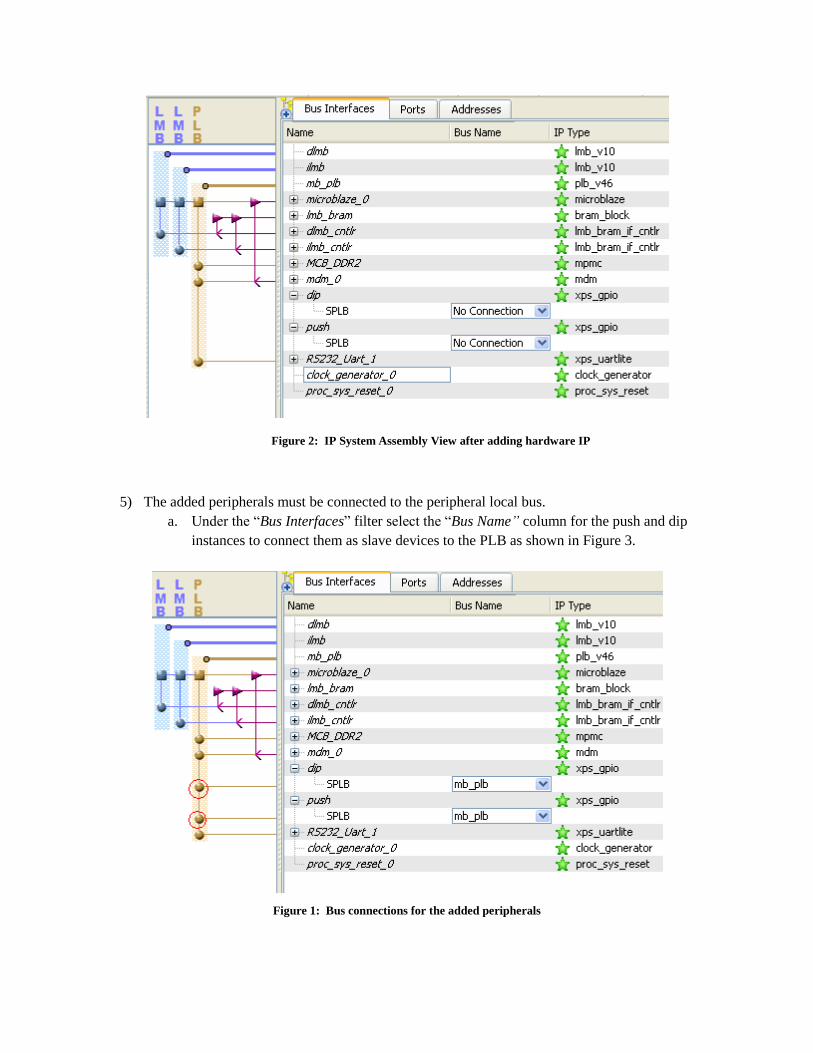
Figure 2: IP System Assembly View after adding hardware IP
5) The added peripherals must be connected to the peripheral local bus.
a. Under the “Bus Interfaces” filter select the “Bus Name” column for the push and dip
instances to connect them as slave devices to the PLB as shown in Figure 3.
Figure 1: Bus connections for the added peripherals
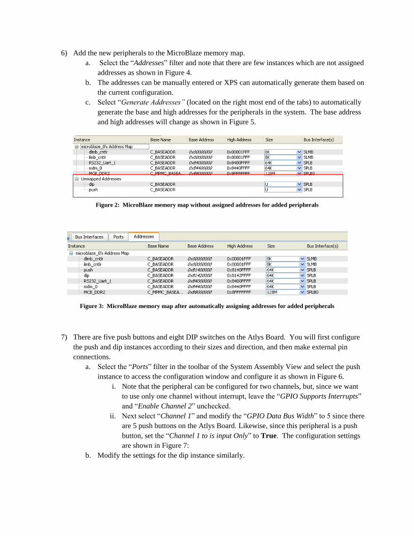
6) Add the new peripherals to the MicroBlaze memory map.
a. Select the “Addresses” filter and note that there are few instances which are not assigned
addresses as shown in Figure 4.
b. The addresses can be manually entered or XPS can automatically generate them based on
the current configuration.
c. Select “Generate Addresses” (located on the right most end of the tabs) to automatically
generate the base and high addresses for the peripherals in the system. The base address
and high addresses will change as shown in Figure 5.
Figure 2: MicroBlaze memory map without assigned addresses for added peripherals
Figure 3: MicroBlaze memory map after automatically assigning addresses for added peripherals
7) There are five push buttons and eight DIP switches on the Atlys Board. You will first configure
the push and dip instances according to their sizes and direction, and then make external pin
connections.
a. Select the “Ports” filter in the toolbar of the System Assembly View and select the push
instance to access the configuration window and configure it as shown in Figure 6.
i. Note that the peripheral can be configured for two channels, but, since we want
to use only one channel without interrupt, leave the “GPIO Supports Interrupts”
and “Enable Channel 2” unchecked.
ii. Next select “Channel 1” and modify the “GPIO Data Bus Width” to 5 since there
are 5 push buttons on the Atlys Board. Likewise, since this peripheral is a push
button, set the “Channel 1 to is input Only” to True. The configuration settings
are shown in Figure 7:
b. Modify the settings for the dip instance similarly.
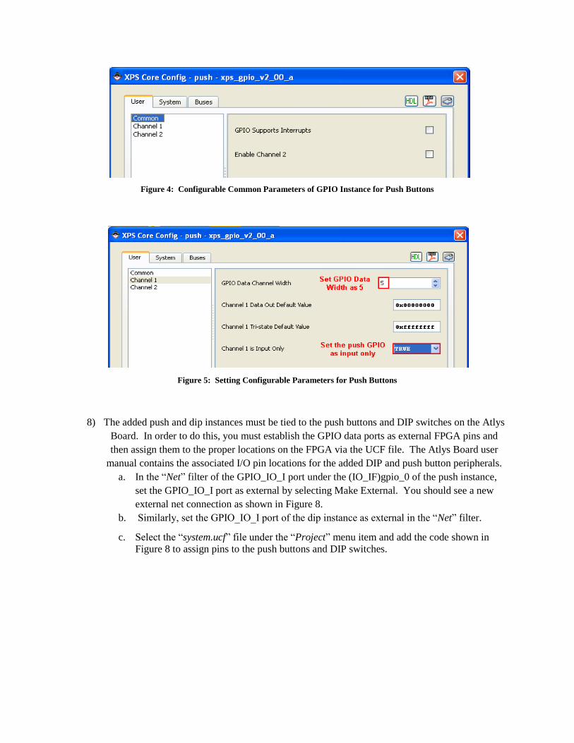
Figure 4: Configurable Common Parameters of GPIO Instance for Push Buttons
Figure 5: Setting Configurable Parameters for Push Buttons
8) The added push and dip instances must be tied to the push buttons and DIP switches on the Atlys
Board. In order to do this, you must establish the GPIO data ports as external FPGA pins and
then assign them to the proper locations on the FPGA via the UCF file. The Atlys Board user
manual contains the associated I/O pin locations for the added DIP and push button peripherals.
a. In the “Net” filter of the GPIO_IO_I port under the (IO_IF)gpio_0 of the push instance,
set the GPIO_IO_I port as external by selecting Make External. You should see a new
external net connection as shown in Figure 8.
b. Similarly, set the GPIO_IO_I port of the dip instance as external in the “Net” filter.
c. Select the “system.ucf” file under the “Project” menu item and add the code shown in
Figure 8 to assign pins to the push buttons and DIP switches.
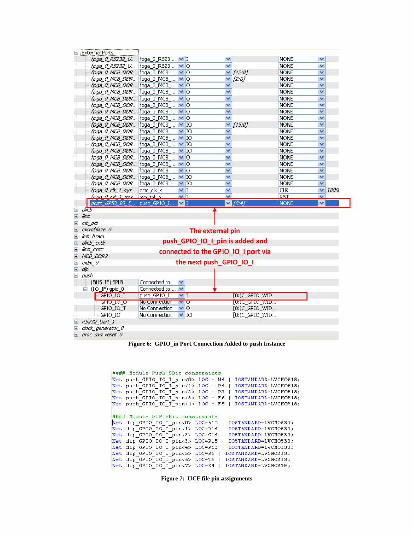
Figure 6: GPIO_in Port Connection Added to push Instance
Figure 7: UCF file pin assignments
The external pin
push_GPIO_IO_I_pin is added and
connected to the GPIO_IO_I port via
the next push_GPIO_IO_I
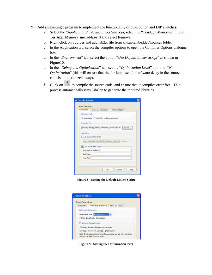
9) Add an existing c program to implement the functionality of push button and DIP switches.
a. Select the “Applications” tab and under Sources, select the “TestApp_Memory.c” file in
TestApp_Memory_microblaze_0 and select Remove.
b. Right click on Sources and add lab2.c file from c:\xup\embedded\sources folder
c. In the Application tab, select the compiler options to open the Compiler Options dialogue
box.
d. In the “Environment” tab, select the option “Use Default Linker Script” as shown in
Figure10.
e. In the “Debug and Optimization” tab, set the “Optimization Level” option to “No
Optimization” (this will ensure that the for loop used for software delay in the source
code is not optimized away).
f. Click on to compile the source code and ensure that it compiles error free. This
process automatically runs LibGen to generate the required libraries.
Figure 8: Setting the Default Linker Script
Figure 9: Setting the Optimization level

10) Download the bitstream to the Atlys Board to verify system operations.
a. Connect the Atlys board to the computer and then power it up.
b. Open a HyperTerminal session from Start All Programs Accessories
HyperTerminal and configure the serial connection for the COM port as shown in
Figure 13 (note that the Atlys board connection is likely COM3 or COM5).
c. Select the “Update Bitstream” option under the “Device Configuration” menu item.
i. This process will take several minutes to synthesize, implement, and generate the
bitstream.
d. Download the bitstream by selecting the “Download Bitstream” option under the “Device
Configuration” menu item.
e. Once the bitstream is downloaded, the DONE LED should be illuminated and the
message shown in Figure 14 should be displayed in the HyperTerminal window.
f. After pressing the push buttons or toggling the switches on the Atlys board, the output
displayed within the HyperTerminal window should change respectively.
Figure 10: HyperTerminal COM port setting to communicate with Atlys board
Figure 11: Response from Atlys board over HyperTerminal upon successful configuration of MicroBlaze system
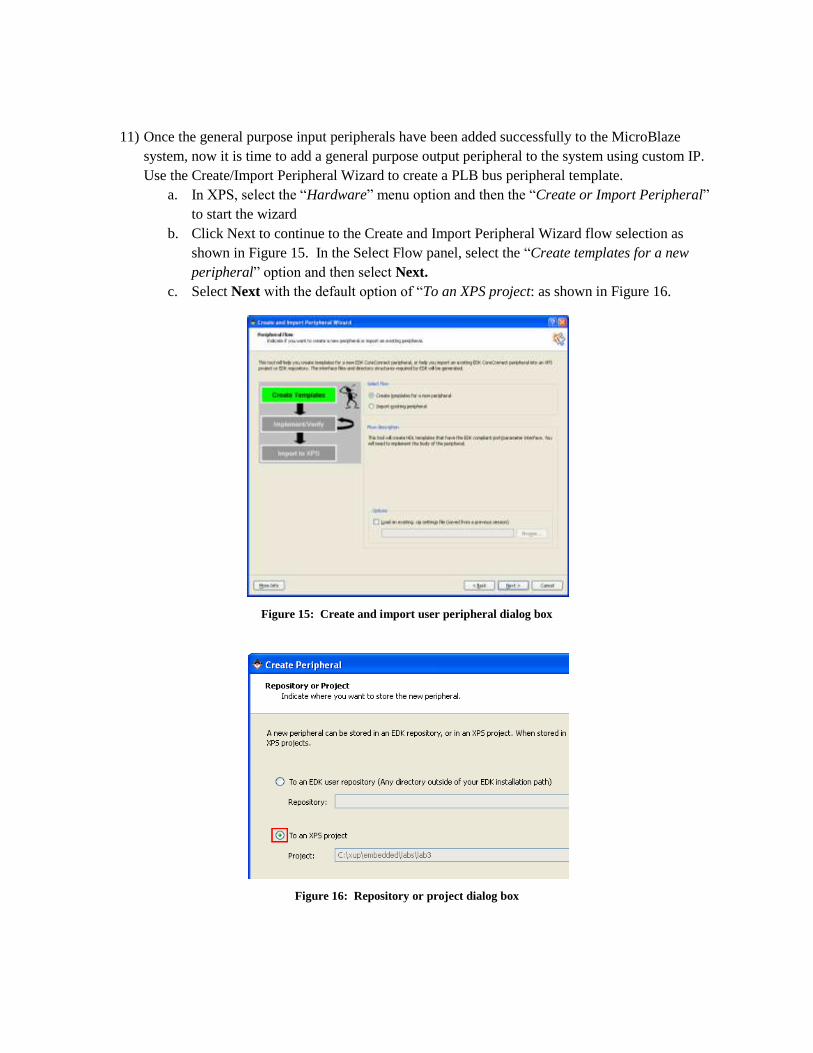
11) Once the general purpose input peripherals have been added successfully to the MicroBlaze
system, now it is time to add a general purpose output peripheral to the system using custom IP.
Use the Create/Import Peripheral Wizard to create a PLB bus peripheral template.
a. In XPS, select the “Hardware” menu option and then the “Create or Import Peripheral”
to start the wizard
b. Click Next to continue to the Create and Import Peripheral Wizard flow selection as
shown in Figure 15. In the Select Flow panel, select the “Create templates for a new
peripheral” option and then select Next.
c. Select Next with the default option of “To an XPS project: as shown in Figure 16.
Figure 15: Create and import user peripheral dialog box
Figure 16: Repository or project dialog box
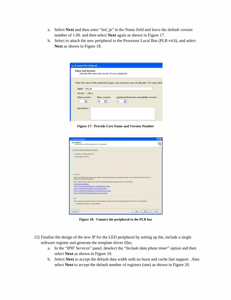
a. Select Next and then enter “led_ip” in the Name field and leave the default version
number of 1.00. and then select Next again as shown in Figure 17.
b. Select to attach the new peripheral to the Processor Local Bus (PLB v4.6), and select
Next as shown in Figure 18.
Figure 17: Provide Core Name and Version Number
Figure 18: Connect the peripheral to the PLB bus
12) Finalize the design of the new IP for the LED peripheral by setting up the, include a single
software register and generate the template driver files.
a. In the “IPIF Services” panel, deselect the “Include data phase timer” option and then
select Next as shown in Figure 19.
b. Select Next to accept the default data width with no burst and cache line support. Also
select Next to accept the default number of registers (one) as shown in Figure 20.
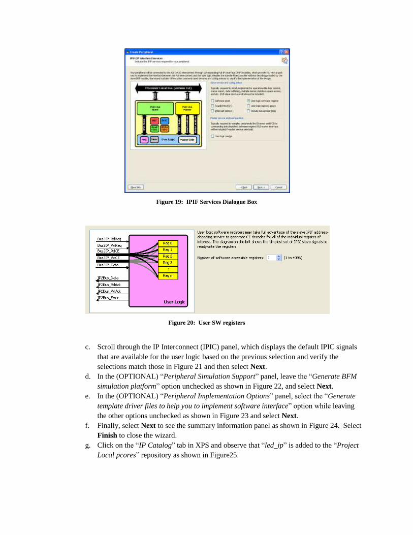
Figure 19: IPIF Services Dialogue Box
Figure 20: User SW registers
c. Scroll through the IP Interconnect (IPIC) panel, which displays the default IPIC signals
that are available for the user logic based on the previous selection and verify the
selections match those in Figure 21 and then select Next.
d. In the (OPTIONAL) “Peripheral Simulation Support” panel, leave the “Generate BFM
simulation platform” option unchecked as shown in Figure 22, and select Next.
e. In the (OPTIONAL) “Peripheral Implementation Options” panel, select the “Generate
template driver files to help you to implement software interface” option while leaving
the other options unchecked as shown in Figure 23 and select Next.
f. Finally, select Next to see the summary information panel as shown in Figure 24. Select
Finish to close the wizard.
g. Click on the “IP Catalog” tab in XPS and observe that “led_ip” is added to the “Project
Local pcores” repository as shown in Figure25.
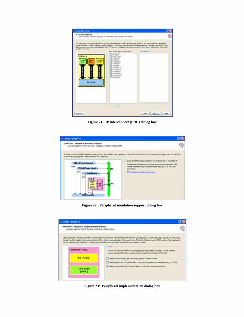
Figure 21: IP interconnect (IPIC) dialog box
Figure 22: Peripheral simulation support dialog box
Figure 23: Peripheral implementation dialog box
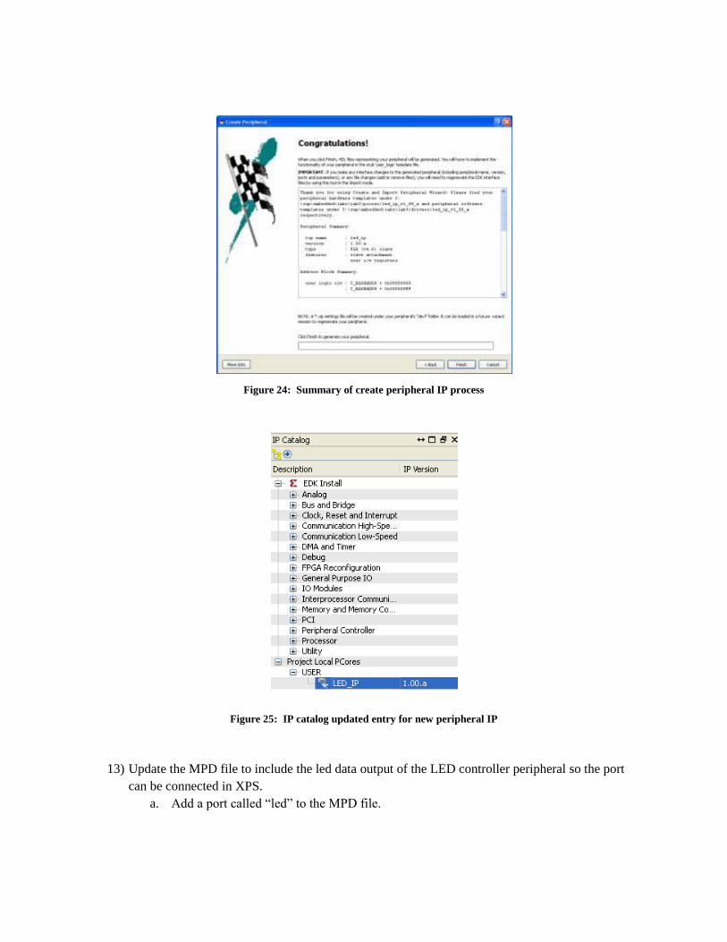
Figure 24: Summary of create peripheral IP process
Figure 25: IP catalog updated entry for new peripheral IP
13) Update the MPD file to include the led data output of the LED controller peripheral so the port
can be connected in XPS.
a. Add a port called “led” to the MPD file.
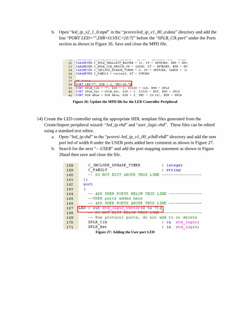
b. Open “led_ip_v2_1_0.mpd” in the “pcores\led_ip_v1_00_a\data” directory and add the
line “PORT LED="",DIR=O,VEC=[0:7]” before the “SPLB_Clk port” under the Ports
section as shown in Figure 26. Save and close the MPD file.
Figure 26: Update the MPD file for the LED Controller Peripheral
14) Create the LED controller using the appropriate HDL template files generated from the
Create/Import peripheral wizard: “led_ip.vhd” and “user_logic.vhd”. These files can be edited
using a standard text editor.
a. Open “led_ip.vhd” in the “pcores\ led_ip_v1_00_a\hdl\vhdl” directory and add the user
port led of width 8 under the USER ports added here comment as shown in Figure 27.
b. Search for the next “—USER” and add the port mapping statement as shown in Figure
28and then save and close the file.
Figure 27: Adding the User port LED
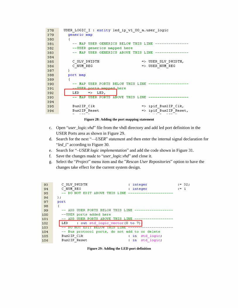
Figure 28: Adding the port mapping statement
c. Open “user_logic.vhd” file from the vhdl directory and add led port definition in the
USER Ports area as shown in Figure 29.
d. Search for the next “—USER” statement and then enter the internal signal declaration for
“led_i” according to Figure 30.
e. Search for “–USER logic implementation” and add the code shown in Figure 31.
f. Save the changes made to “user_logic.vhd” and close it.
g. Select the “Project” menu item and the ”Rescan User Repositories” option to have the
changes take effect for the current system design.
Figure 29: Adding the LED port definition
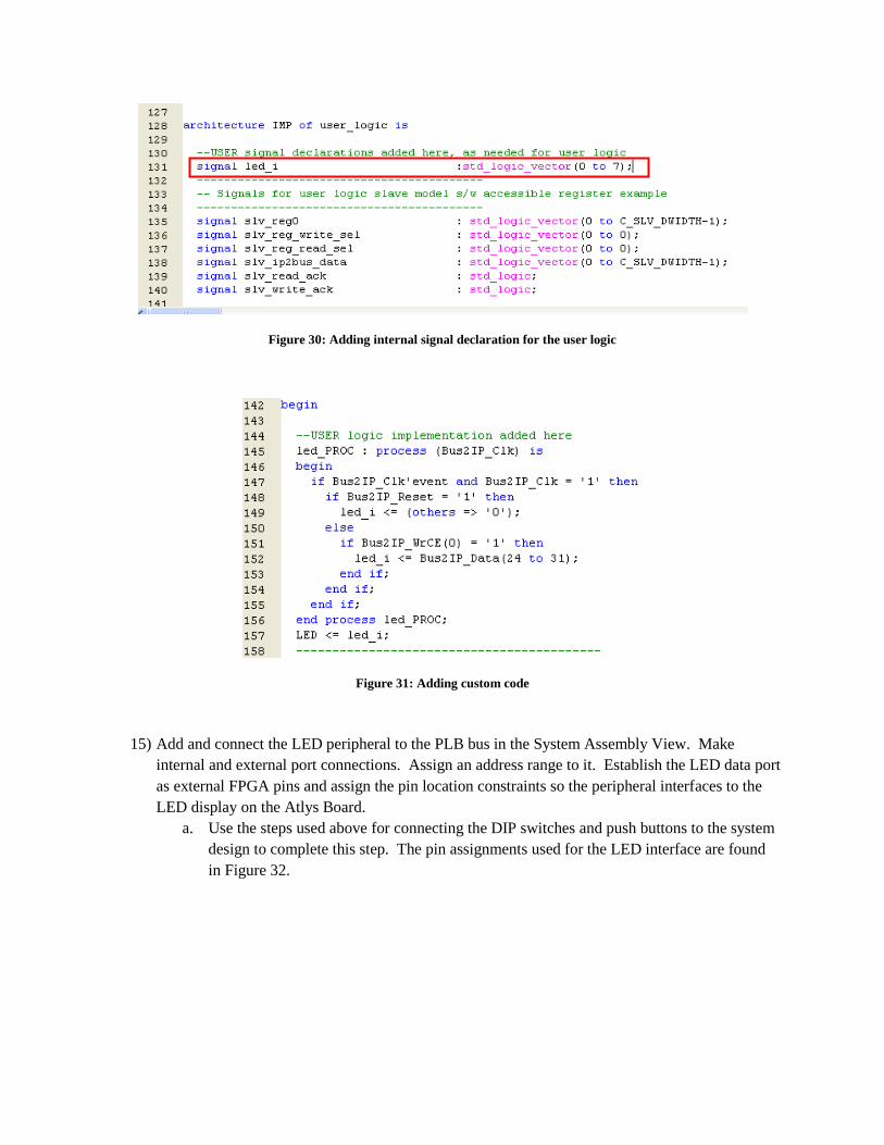
Figure 30: Adding internal signal declaration for the user logic
Figure 31: Adding custom code
15) Add and connect the LED peripheral to the PLB bus in the System Assembly View. Make
internal and external port connections. Assign an address range to it. Establish the LED data port
as external FPGA pins and assign the pin location constraints so the peripheral interfaces to the
LED display on the Atlys Board.
a. Use the steps used above for connecting the DIP switches and push buttons to the system
design to complete this step. The pin assignments used for the LED interface are found
in Figure 32.
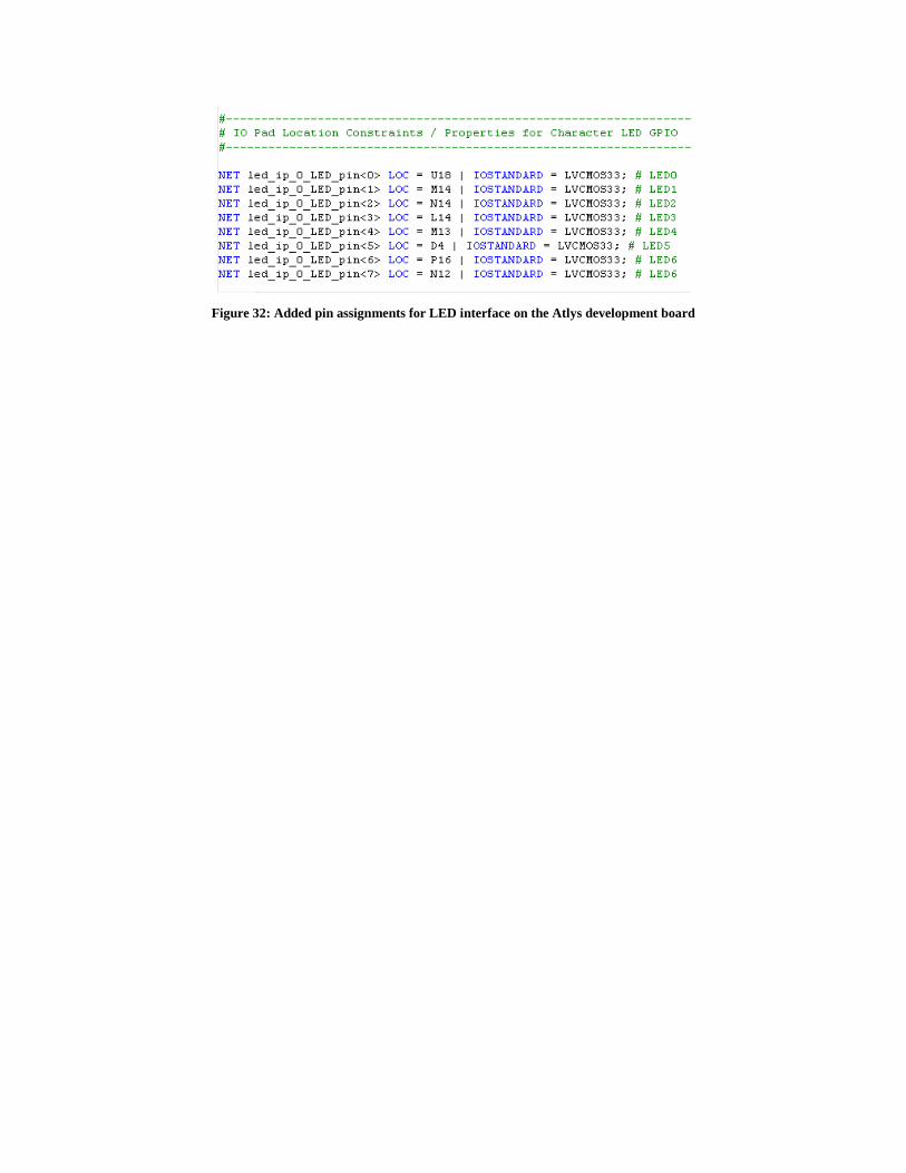
Figure 32: Added pin assignments for LED interface on the Atlys development board