Embed Size (px)
Citation preview
ÉCOLE DE TECHNOLOGIE SUPÉRIEURE UNIVERSITÉ DU QUÉBEC
THESIS PRESENTED TO ÉCOLE DE TECHNOLOGIE SUPÉRIEURE
IN PARTIAL FULFILLMENT OF THE REQUIREMENTS FOR THE DEGREE OF DOCTOR OF PHILOSOPHY
Ph.D.
BY Sabeur LAFI
A NEW HARDWARE ABSTRACTION-BASED RADIOFREQUENCY DESIGN METHODOLOGY: FOUNDATIONS AND CASE STUDIES
MONTREAL, NOVEMBER 15, 2016
© Copyright Sabeur Lafi, 2016 All rights reserved

© Copyright
Reproduction, saving or sharing of the content of this document, in whole or in part, is prohibited. A reader
who wishes to print this document or save it on any medium must first obtain the author’s permission.
BOARD OF EXAMINERS
THIS THESIS HAS BEEN EVALUATED
BY THE FOLLOWING BOARD OF EXAMINERS Mr. Ammar Kouki, Thesis Supervisor Département de Génie Électrique at École de technologie supérieure Mr. Jean Belzile, Thesis Co-supervisor Département de Génie Électrique at École de technologie supérieure Mr. Roger Champagne, Chair, Board of Examiners Département de Génie Logiciel at École de technologie supérieure Mr. Claude Thibeault, Member of the jury Département de Génie Électrique at École de technologie supérieure Mr. Roni Khazaka, External Evaluator Electrical and Computer Engineering Department at McGill University
THIS THESIS WAS PRESENTED AND DEFENDED
IN THE PRESENCE OF A BOARD OF EXAMINERS AND THE PUBLIC
SEPTEMBER 16, 2016
AT ÉCOLE DE TECHNOLOGIE SUPÉRIEURE


ACKNOWLEDGMENTS
First and foremost, I would like to express my sincerest and deepest gratitude to my supervisor
Prof. Ammar Kouki for his continuous and generous support of my PhD studies and research.
I immensely appreciate his understanding, motivation and patience as well as his efforts for
providing me with the required resources and an excellent atmosphere for doing my research.
I also acknowledge his vast expertise, and immense knowledge, which added considerably to
my graduate experience. His valuable guidance and advices helped me in all my research
activities and throughout the writing process of this thesis.
Besides my advisor, I would like to thank my co-supervisor Prof. Jean Belzile for his constant
encouragement, insightful guidance, and continuous support all over my graduate studies and
research. I particularly appreciate his significant contribution to this research work and his
focused comments that enhanced the quality of my text.
I extend my gratitude to the rest of my thesis committee: Prof. Roger Champagne, Prof. Claude
Thibeault, and Prof. Roni Khazaka, for their encouragement, insightful comments, and kind
acceptance to evaluate my PhD work.
My sincere thanks goes also to Mr. Frank Ditore, Mr. Rulon Vandyke, and all the Alpharetta-
based team of Keysight Technologies Inc., for offering me an extended summer internship in
2012 and leading my work on diverse exciting projects.
I also acknowledge the generous financial support of LACIME (Laboratoire de
Communications et d’Intégration de la Microélectronique), the BREM (Bureau du
Recrutement Étudiant et de la Mobilité de l'ÉTS), and CREER (Centre de Recherche En
Électronique Radiofréquence) in conjunction with FQRNT (Fonds de Recherche du Québec –
Nature et Technologies).
Last but not the least, I thank all my fellow labmates at LACIME and in particular, Ahmed
Elzayet, for his valuable comments and remarks. I am also grateful to LACIME staff for
providing an excellent work atmosphere.

VI
Finally, I would like to thank my parents and family for their faithful encouragement,
unceasing support and best wishes and in particular, I must acknowledge the role of my wife
and best friend, Fatma, without whose love, devotion and understanding, I would not have
finished this thesis.
NOUVELLE MÉTHODOLOGIE BASÉE SUR L’ABSTRACTION MATÉRIELLE POUR LA CONCEPTION RADIOFRÉQUENCE: BASES ET ÉTUDES DE CAS
Sabeur LAFI
RÉSUMÉ
Les dispositifs de communication sans fils connaissent une croissance soutenue due au succès et à la popularité des téléphones portables auprès du grand public. De plus, l’émergence d’applications et services mobiles semble accroître les attentes du consommateur concernant les performances et les fonctionnalités des prochaines générations d’appareils sans fils. En outre, la multitude des normes de télécommunications, l’encombrement du spectre électromagnétique et les interférences complexifient la conception des systèmes radios. Pour réduire cette complexité, des avancées ont été enregistrées au niveau des technologies, des outils et des processus de conception de la partie numérique de la radio. Toutefois, bien que plusieurs technologies prometteuses soient en cours de mise au point au niveau de la partie radiofréquence, les améliorations des approches de conception et des outils qui y sont associés reçoivent beaucoup moins d’attention. Ce travail vise à pallier à ce déficit en s’attaquant particulièrement aux problématiques de productivité et de collaboration entre concepteurs des systèmes radiofréquences ainsi qu’à l’automatisation des tâches de conception. Pour atteindre cet objectif, nous cherchons à explorer une approche de conception réduisant la dépendance aux détails physiques et élevant le niveau d’abstraction de manière à découpler la fonctionnalité à concevoir de la technologie d’implémentation. De ce fait, nous proposons dans cette thèse une nouvelle approche de conception des circuits et systèmes radiofréquences se basant sur l’abstraction matérielle. Dans un premier lieu, nous présentons une revue critique des approches actuelles. Ensuite, nous détaillons les concepts de l’approche proposée, notamment son cycle de conception, la stratégie d’abstraction matérielle qui lui est associée et la matrice Q. Puis, nous finissons ce travail par des études de cas où nous essayons de valider les concepts susmentionnées. Mots-clés: méthodologie de conception radiofréquence, abstraction matérielle, matrice Q, modélisation en SysML, vérification de cohérence, transformation de modèles

A NEW HARDWARE ABSTRACTION-BASED RADIOFREQUENCY DESIGN METHODOLOGY: FOUNDATIONS AND CASE STUDIES
Sabeur LAFI
ABSTRACT
The need for radio systems is in growth due to the particular success of cellular and wireless devices. On the one hand, the emergence of new applications and services raises consumer expectations regarding future radio systems’ performance. On the other hand, radio design is becoming more challenging due to multi-standard functionality, spectrum crowdedness and harsh operating environments. In order to keep pace with the emerging requirements, notable advances have taken place in digital design either in implementation technologies or in design approaches and tools. On the radiofrequency side, many promising technologies are being developed to enhance radio systems capability but little interest is dedicated to the improvement of design approaches and tools. To bridge this gap, several design challenges should be addressed especially in terms of productivity, design collaboration, automation and reuse as well as ensuring better technology insertion. To tackle all these challenges, it is necessary to ameliorate the design approaches, overcome technology-dependence and raise the abstraction level in today’s radiofrequency design practice in order to decouple the radio functionality from the underlying technology. In the light of this observation, we dedicate this thesis to the elaboration of a new radiofrequency design methodology based on hardware abstraction. Its first section investigates the limitations of current RF design tools and approaches. The following one presents an alternative framework that tackles the issues of automation, design collaboration and reuse. The proposed framework is based on a comprehensive abstraction strategy that combines intensive modeling activity and handful abstraction mechanisms to enable higher design automation and agility. The last section is dedicated to the validation of the proposed framework through selected case studies. Keywords: RF design methodology, hardware abstraction, Q-matrix, functional description, SysML modeling, coherence verification, model-to-model transformation

TABLE OF CONTENTS
Page
INTRODUCTION .....................................................................................................................1
CHAPTER 1 BACKGROUND .........................................................................................9 1.1 Introduction ....................................................................................................................9 1.2 Back to the Beginnings of Wireless and Mobile Communications .............................10
1.2.1 Historical Perspective ............................................................................... 10 1.2.2 Evolution of Wireless and Mobile Communications ................................ 11
1.3 Future Trends in Wireless and Mobile Communications and Subsequent Impact on Technology and Design Approaches and Tools .........................................17 1.3.1 Trends in Wireless and Mobile Communications ..................................... 17 1.3.2 Impact on Technology and Design Approaches and Tools ...................... 20
1.4 Challenges in Wireless and Mobile Radio Design ......................................................29 1.5 Conclusion ...................................................................................................................38
CHAPTER 2 COMPARATIVE STUDY OF COMMON DESIGN APPROACHES ....43 2.1 Introduction ..................................................................................................................43 2.2 Common Design Approaches and Future Requirements in Design Tools ..................44
2.2.1 Common Design Approches ..................................................................... 44 2.2.2 Future Requirements in Design Tools ...................................................... 47
2.3 Lessons to be learned from Current Design Practice ...................................................48 2.3.1 Digital Design ........................................................................................... 49 2.3.2 Analog and Mixed-Signal Design ............................................................. 56 2.3.3 RF and Microwave Design ....................................................................... 60
2.4 Comparative Study of Design Practice through Domains ...........................................72 2.5 Conclusion ...................................................................................................................77
CHAPTER 3 THE PROPOSED FRAMEWORK FOR RF AND MICROWAVE DESIGN ...........................................................................79
3.1 Introduction ..................................................................................................................79 3.2 Scope and Objectives ...................................................................................................80 3.3 Proposal of a New Framework to Bridge Existing Design Gaps.................................81
3.3.1 A Five-Step Design Scheme ..................................................................... 82 3.3.2 Functional Description .............................................................................. 82 3.3.3 Analysis..................................................................................................... 90 3.3.4 Synthesis ................................................................................................... 96 3.3.5 Q-matrix .................................................................................................. 104 3.3.6 Summary View of the Proposed Design Flow ........................................ 122
3.4 Mapping Framework Provisions to Designated Design Challenges ..........................124 3.5 Conclusion .................................................................................................................127
XII
CHAPTER 4 HARDWARE ABSTRACTION-BASED STRATEGY FOR RF AND MICROWAVE DESIGN .........................................................129
4.1 Introduction ................................................................................................................129 4.2 Hardware Abstraction in Various Domains ...............................................................130
4.2.1 Definition and Advantages ..................................................................... 130 4.2.2 Hardware Abstraction in Digital and Mixed-Signal Design ................... 133 4.2.3 Hardware Abstraction in Computer Engineering ................................... 148 4.2.4 Hardware Abstraction in Software Engineering ..................................... 153 4.2.5 Hardware Abstraction in Other Domains ............................................... 178
4.3 Proposed RF and Microwave Hardware Abstraction Strategy ..................................180 4.3.1 Scope and Objectives .............................................................................. 180 4.3.2 Basic Definitions ..................................................................................... 181 4.3.3 Functional Description of RF and Microwave Systems:
Black-Box Model .................................................................................... 182 4.3.4 Abstraction Levels, Viewpoints and Views ............................................ 196 4.3.5 Transition between Abstraction Levels .................................................. 210
4.4 Application to RF and Microwave Design ................................................................229 4.5 SysML Profile for RF Devices ..................................................................................233
4.5.1 RF Stereotypes ........................................................................................ 234 4.5.2 Coherence Rules and Requirements ....................................................... 240 4.5.3 Profile Extension and Usage ................................................................... 248
4.6 Integration of RF and Microwave Hardware Abstraction Strategy in the Proposed Design Framework ...............................................................................251
4.7 Provision of the RF and Microwave Hardware Abstraction Strategy within the Proposed Design Framework ....................................................................254
4.8 Conclusion .................................................................................................................258
CHAPTER 5 VALIDATION OF THE PROPOSED FRAMEWORK THROUGH SELECTED CASE STUDIES .................................................................261
5.1 Introduction ................................................................................................................261 5.2 Practical Implementation of the Proposed Framework ..............................................262 5.3 Case Studies ...............................................................................................................267
5.3.1 Frequency Selection Device ................................................................... 267 5.3.2 Power Attenuation Device ...................................................................... 361 5.3.3 Frequency Translation Device ................................................................ 392
5.4 Conclusion .................................................................................................................423
CONCLUSION ......................................................................................................................425
APPENDIX I HISTORY AND ADVANTAGES OF MODERN ELECTRONIC DESIGN AUTOMATION TOOLS .........................................................433
APPENDIX II OVERVIEW OF SYSTEMS MODELING LANGUAGE......................439
APPENDIX III SUMMARY OF EQUATIONS AND FORMULAS USED IN CASE STUDIES ......................................................................................451

XIII
LIST OF REFERENCES .......................................................................................................461

LIST OF TABLES
Page Table 1.1 Strengths and weaknesses in digital, analog/mixed-signal and
RF/microwave design .......................................................................................40
Table 1.2 Strengths and weaknesses in digital, analog/mixed-signal and RF/microwave design (Table 1.1 cont’d) .........................................................41
Table 2.1 Comparison between bottom-up and top-down design approaches .................47
Table 2.2 Comparison of some characteristics of digital, analog/mixed-signal and RF/microwave domains ....................................................................................74
Table 2.3 Comparison of digital, analog/mixed-signal and RF/microwave design practice ..................................................................................................78
Table 3.1 Summary of the properties that the intended RF design framework is expected to support ...........................................................................................81
Table 3.2 An example of XML structure to capture the SysML model of Figure 3.4 .....89
Table 3.3 Relationships between bandpass filter parameters given in Figure 3.6 ...........94
Table 3.4 An example of coherence rules to validate a typical RF filter functional description .......................................................................................94
Table 3.5 A selection of RF filter integrity control rules .................................................94
Table 3.6 Overview of the Q-matrix XML data structure ..............................................111
Table 3.7 How the proposed framework addressed the requirements expressed in Table 3.1 ....................................................................................126
Table 4.1 Views are associated to viewpoints and models ............................................172
Table 4.2 RF systems can be viewed as black-boxes with inputs and outputs ..............185
Table 4.3 RF and microwave systems can be modeled using response functions .........188
Table 4.4 Atomic components’ layer is composed of atomic components (i.e., RF indivisible devices) ...........................................................................201
Table 4.5 Examples of equation-based transformations for T- and π-pad attenuators design ...........................................................................................215
XVI
Table 4.6 Variable weights are estimated based on property constraints .................224
Table 4.7 Performance details of two candidate design solutions for the GPS bandpass filter of Figure 3.4 ..................................................................226
Table 4.8 Calculation of the objective function for each candidate design solution ......227
Table 4.9 Comparison between the proposed abstraction strategy for RF/microwave design and those adopted for MDE/MDA, digital, analog and mixed-signal design .....................................................................256
Table 4.10 How the proposed hardware abstraction helps the framework in tackling the requirements given in Table 3.1 .................................................257
Table 5.1 List of case studies .........................................................................................270
Table 5.2 Typical bandpass filter requirements for a 450-MHz satellite radio ..............275
Table 5.3 List of bandpass filter value properties as presented in the bdds of Figure 5.10 and 5.11 .......................................................................................282
Table 5.4 List of bandpass filter port value properties as presented in the bdd of Figure 5.10 .................................................................................................283
Table 5.5 Relationships between bandpass filter parameters given in Figure 5.24 .......297
Table 5.6 Main filter electrical consistence rules ...........................................................297
Table 5.7 Bandpass filter PIM-level design constraints rules ........................................299
Table 5.8 Bandpass filter integrity control rules ............................................................299
Table 5.9 Black-box model: performance summary of the four filter prototypes .........305
Table 5.10 Constant weights and property constraints for each decision variable ..........307
Table 5.11 Objective function calculations for each filter prototype ...............................310
Table 5.12 PIM-to-PSM transformation (target platform: LC/distributed lines) .............311
Table 5.13 Overview of the intra-view transformation for granularity refinement .........316
Table 5.14 Electrical models for non-ideal inductors and capacitors ..............................319
Table 5.15 List of inductors found in the technology library during automated technology mapping .......................................................................................326
XVII
Table 5.16 List of capacitors found in the technology library during automated technology mapping .......................................................................................327
Table 5.17 Comparison of PCB areas required to hold the generated platform models ..............................................................................................333
Table 5.18 Lowpass filter specifications ..........................................................................343
Table 5.19 List of lowpass filter value properties (port value properties are not considered) ...............................................................................................346
Table 5.20 Relationships between lowpass filter value properties given in Figure 5.54 .....................................................................................................349
Table 5.21 A PIM to PSM transformation for stepped-impedance lowpass filters .........352
Table 5.22 A PIM-to-PSM transformation based on open-end circuit stubs ...................353
Table 5.23 Calculations resulting from the stepped-impedance-based (PIM-to-PSM) transformation ........................................................................354
Table 5.24 Main properties of the RO3006 substrate ......................................................354
Table 5.25 Lowpass stepped-impedance filter PM form factor .......................................355
Table 5.26 Calculations resulting from the open-end stub-based transformation ............359
Table 5.27 Lowpass open-end stub-based filter PM form factor .....................................360
Table 5.28 Typical specifications of a 3-dB RF attenuator ..............................................362
Table 5.29 List of values of « Attenuator » block ............................................................367
Table 5.30 List of values of each « Port » block ..............................................................368
Table 5.31 Relationships between attenuator parameters given in Figure 5.71 ...............372
Table 5.32 Attenuator integrity control rules ...................................................................372
Table 5.33 PIM-to-PSM transformation for T and Π resistive attenuators ......................375
Table 5.34 Values of resistors for T and Π attenuators ....................................................375
Table 5.35 T attenuator initial resistors ............................................................................384
Table 5.36 Π attenuator initial resistors ...........................................................................384
Table 5.37 T attenuator alternative resistors ....................................................................385
XVIII
Table 5.38 Π attenuator alternative resistors. ...................................................................386
Table 5.39 Form factor of initial and refined PIMs for both T and Π attenuators ...........387
Table 5.40 Intra-view transformation used for the attenuators’ PSM granularity refinement ....................................................................................388
Table 5.41 Mixer specifications .......................................................................................392
Table 5.42 List of mixer value properties as presented in the corresponding bdds .........396
Table 5.43 List of mixer port value properties as enumerated in the SysML models ......397
Table 5.44 Mixer PIM-level design constraints rules ......................................................401
Table 5.45 Common relationships between mixer parameters given in Figure 5.87 .......403
Table 5.46 Mixer integrity control rules ..........................................................................403
Table 5.47 Passive diode mixer PIM-to-PSM transformation .........................................407
Table 5.48 Rat-race Mixer PIM to PSM transformation ..................................................407
Table 5.49 Generated PSMs: Summary of both mixer PSMs performance characteristics ............................................................................413
Table 5.50 Generated PSMs: Objective function calculations for each filter prototype ................................................................................................413
Table 5.51 Properties of the synthesized rat-race microstrip sections (RO3006 substrate) ........................................................................................414
Table 5.52 List of suitable diode parts found in the technology library ..........................415
Table 5.53 List of inductor parts found in the technology library during automated technology mapping .......................................................................................417
Table 5.54 List of capacitor parts found in the technology library during automated technology mapping .......................................................................................417
Table 5.55 Comparison of the performance of the three PSM prototypes .......................418
Table 5.56 Technology mapped PSM: Objective function calculations for each rat-race mixer prototype .................................................................................419
LIST OF FIGURES
Page
Figure 1.1 A non-exhaustive list of milestones in telecommunications history ................12
Figure 1.2 A comparison between the first handheld mobile phone and a recent smartphone ............................................................................................14
Figure 1.3 Evolution of wireless and mobile standards .....................................................16
Figure 1.4 User expectations can be derived into technology and design requirements ..........................................................................................21
Figure 1.5 Radio-communication technology is evolving at a growing pace ...................28
Figure 1.6 A typical multimode, multi-band handset block diagram ................................29
Figure 1.7 iPhone 4 PCB Layout: (a) Front Panel: Front-End components (b) Back Panel: Baseband components ............................................................30
Figure 1.8 A typical multi-standard multi-mode multi-band baseband chip: Qualcomm MDM9615M baseband modem used in iPhone 5 .........................31
Figure 1.9 Interaction between design constraints, methodologies and abstraction levels ..............................................................................................31
Figure 1.10 Design domains ................................................................................................32
Figure 1.11 Challenges in RF design can be fully or partially related to either the design flows or tools in use ........................................................................37
Figure 2.1 An overview of EDA history ...........................................................................49
Figure 2.2 Typical design flow for digital circuits ............................................................53
Figure 2.3 Typical analog design flow using Cadence commercial package ....................57
Figure 2.4 Typical analog and mixed-signal design cycle including common EDA tools in use ..............................................................................................59
Figure 2.5 Main disciplines related to RF design ..............................................................61
Figure 2.6 Overview of some technologies of which typical components in a direct-conversion transceiver are made ............................................................63
XX
Figure 2.7 Intermodulation and nonlinearity: (a) Output power compression and intermodulation distortion in RF amplifier (b) RF mixer spurious products ..............................................................................................64
Figure 2.8 Multiple antagonistic parameters are tuned in RF design ................................65
Figure 2.9 Common trade-offs encountered in RF passives design ..................................66
Figure 2.10 The traditional RF design space is subdivided into two domains (i.e., electrical and physical) with two corresponding representations (i.e., system and circuit) ...................................................................................67
Figure 2.11 Typical RF design scheme and some EDA tools in use for each design stage ..............................................................................................68
Figure 2.12 EDA tools from Agilent Technologies .............................................................70
Figure 2.13 EDA tools from Applied Wave Research ........................................................71
Figure 3.1 The design flow consists of five distinct design stages ....................................83
Figure 3.2 A filter can be modeled in a variety of ways ....................................................85
Figure 3.3 Typical specifications of a GPS L1 RF filter ...................................................87
Figure 3.4 An example of SysML model for a RF filter: (a) the package diagram (b) the value types package (c) the block definition diagram of the filter (d) the requirements diagram ...........................................................................88
Figure 3.5 Functional description is based on high-level modeling ..................................90
Figure 3.6 Parameters relationships graph corresponding to the GPS bandpass filter of Figure 3.4 ............................................................................................93
Figure 3.7 Example of coherence rules to validate a RF filter functional description: (a) A warning results from a rule that detects a minor consistency issue, while (b) an error indicates a major incoherence that makes the design not feasible .......................................................................................................95
Figure 3.8 Example of system-level analyses related to the GPS L1 bandpass filter (considering a 3-dB ripple): (a) ideal filter network (b) transmission and reflection magnitude, (c) phase and (d) group delay ........................................97
Figure 3.9 “Analysis” step includes “Coherence Verification” and system-level “Performance Simulation” ...............................................................................98
XXI
Figure 3.10 Illustration of the granularity refinement concept: (a) and (b) RF amplifier structures, (c) and (d) RF duplexer structures ..................................99
Figure 3.11 Granularity concept applied to the GPS L1 bandpass filter: (a) four lumped-component elements or (b) two resonators .......................................100
Figure 3.12 Some technology parameters required for (a) lumped-component (b) microstrip and (c) coaxial-cable circuits’ implementation .......................102
Figure 3.13 The layout corresponding to microstrip coupled-line realization of the GPS L1 bandpass filter: (a) microstrip physical dimensions (considering a FR-4 substrate), (b) the layout produced using Agilent ADS and (c) its performance simulation using Momentum ..........................................103
Figure 3.14 Synthesis allows nested granularity refinement and technology mapping in order to build ready-for-manufacturing implementations from an elaborated functional description ...................................................................104
Figure 3.15 Linking the different design stages with the Q-matrix to handle data exchange .................................................................................................107
Figure 3.16 Conventions used in a typical two-port RF network where 1 ≠ 2 ..........108
Figure 3.17 Generalized Q-matrix is a function of frequency, power, temperature and time ......................................................................................110
Figure 3.18 The file consists of various data blocks composing data of different sources .............................................................................................112
Figure 3.19 Q-matrix data blocks from different data sources ..........................................112
Figure 3.20 Hierarchical structure of a data block ............................................................113
Figure 3.21 Examples of data blocks usage and possibilities of metadata extensibility ...114
Figure 3.22 A usage example showing how the Q-matrix XML structure captures passive device’s linear response: (a) RF filter model, (b) its corresponding Q-matrix and (c) data representation ..........................116
Figure 3.23 VCO’s Q-matrix XML structure: (a) A voltage-controlled oscillator model, (b) its formal Q-matrix, (c) an example of a VCO circuit ..................117
Figure 3.24 VCO’s Q-matrix XML structure (cont’d): (a) the configuration section and (b) the data section (limited to only two points of control and output voltages) ..............................................................................................118
XXII
Figure 3.25 Q-matrix XML structure is also able to capture amplifier I-V data: (a) Amplifier model, (b) its corresponding Q-matrix and (c) an example of an amplifier circuit ............................................................120
Figure 3.26 Q-matrix XML structure is also able to capture amplifier I-V data: The data file corresponding to the amplifier model of Figure 3.25 ...............121
Figure 3.27 The proposed framework for RF and microwave design ...............................123
Figure 4.1 Every abstraction level corresponds to a new representation (i.e., model) ....134
Figure 4.2 The five abstraction levels in digital circuit design correspond to five abstraction views subdivided into three distinct design domains ..................137
Figure 4.3 The three-domain five-abstraction-level Gajski-Kuhn’s Y-chart ..................138
Figure 4.4 A digital functionality design changes its representation when it gradually goes through the behavioral, structural and physical domains ......141
Figure 4.5 A top-down design flow mapped to the abstraction levels and design domains of Gajski-Kuhn’s Y-chart results in a back and forth top-down process ............................................................................................142
Figure 4.6 Raising the abstraction levels allowed more complex device models ...........142
Figure 4.7 Design automation tools, IC technologies and design methodologies in microelectronics have evolved jointly with abstraction levels .......................143
Figure 4.8 Higher abstraction levels enable the design of more complex chips .............143
Figure 4.9 Notable differences between abstraction levels in digital and analog/mixed-signal design ............................................................................145
Figure 4.10 A specific simulation type corresponds to each abstraction levels in analog/mixed-signal design ............................................................................146
Figure 4.11 An example of how abstraction levels are applied to analog/mixed-signal design: A differential operational amplifier design starts as HDL description at functional level and ends with a useful layout at circuit level ................................................................147
Figure 4.12 Each abstraction level corresponds to simulation type that is more time-consuming but accurate from higher to lower levels .....................................148
Figure 4.13 The hardware abstraction layer plays a mediation role between the operating system (and user applications) and the physical hardware .....150
XXIII
Figure 4.14 Modern networks were built upon a layered architecture based on OSI and TCP/IP networking models .....................................................................151
Figure 4.15 Modern databases use at least three abstraction levels to manage the stored data and control the interaction of users with them .......................152
Figure 4.16 Evolution of abstraction levels in programming languages ...........................156
Figure 4.17 Impact of abstraction level rise on productivity and code reuse: (a) from one source for one system architecture to one model to multiple hardware/software platforms (b) Source code reuse started with functions and evolved towards domain models .....................................158
Figure 4.18 The modular programming paradigm subdivides a software system into independent, shared and reusable components ..............................................159
Figure 4.19 Abstraction through objects and classes: (a) real-world objects and (b) how they are modeled using a UML class diagram ..................................162
Figure 4.20 MDE enables the use of automated model-to-model transformation tools to enhance the automation of design steps ............................................167
Figure 4.21 The model-driven architecture defines two types of models at different abstraction levels ............................................................................................169
Figure 4.22 In MDE/MDA, a meta-model abstracts a model which itself abstracts a real-world reality .........................................................................................171
Figure 4.23 Automation process in MDE/MDA framework encompasses four abstraction levels and three model-to-model transformations ................175
Figure 4.24 Model-to-Model transformation in MDE/MDA ............................................175
Figure 4.25 Model-to-Model transformation: (a) PIM to PSM transformation and (b) transformation bridges ..............................................................................176
Figure 4.26 An example of PIM to PSM mapping: (a) UML to C# Transformation (b) The same PIM (i.e., UML models) is transformed into three PSMs (corresponding to three different source code representations) given the relevant platform specifications .....................................................................177
Figure 4.27 An excerpt of the UML profile for software radios: a logical-physical channel stereotype abstracts devices that provide analog communications (e.g., RF) .............................................................................179
Figure 4.28 A black-box view considers a RF system as an entity which is defined by its inputs/outputs and its response function ...............................................183
XXIV
Figure 4.29 SysML black-box model of a RF system .......................................................192
Figure 4.30 The block diagram of a UMTS FDD transceiver ...........................................193
Figure 4.31 SysML allows the expression of different aspects in RF systems: (a) package diagram (b) the transceiver’s associated block definition diagram ..........................................................................................194
Figure 4.32 SysML allows the expression of different aspects in RF systems (cont’d): (a) the receiver’s internal block diagram (b) the duplex filter specifications (c) the duplex filter requirements diagram ..............................195
Figure 4.33 Four abstraction levels are considered in the proposed RF hardware abstraction strategy: System, module, circuit and atomic components ..........200
Figure 4.34 The atomic layer is composed of "leaf" electrical devices whose functions are not indivisible ...........................................................................201
Figure 4.35 An example of how the different abstraction levels are considered in a typical RF system ....................................................................................205
Figure 4.36 A viewpoint corresponds to an abstract design perspective while a view specifies a representation (i.e., model) which complies with that design perspective ..........................................................................................207
Figure 4.37 Four abstraction views are associated to four abstraction viewpoints and four abstraction levels ..............................................................................209
Figure 4.38 Two transformations are defined to move from system requirements throughout implementation ............................................................................210
Figure 4.39 Cross- and intra-view transformations ...........................................................214
Figure 4.40 Granularity is all about the level of detail within an abstraction view: (a) the system is composed of seven blocks (b) one of these seven blocks can be broken up into eight other parts ...............................................216
Figure 4.41 A system-level model of a direct-conversion receiver can be partitioned in modules in different ways of different granularity levels ..........................217
Figure 4.42 Two examples of granularity level expressed using SysML block definition diagram: (a) An amplifier is considered as whole [Granularity level = 1] (b) An amplifier is considered as an assembly of amplification, matching, and biasing networks [Granularity level = 4] .........219
Figure 4.43 Reversible platform-specific model for resistive attenuators .........................220
XXV
Figure 4.44 Granularity refinement: (a) Unbalanced to balanced T and (b) π attenuator transformations .....................................................................222
Figure 4.45 An example of overriding a default constraint property using a new equation for the calculation of variable weights .....................................225
Figure 4.46 The four abstraction views can be mapped to traditional passive RF filters design steps ....................................................................................229
Figure 4.47 An example of transformation scheme for operational amplifier design .......232
Figure 4.48 The proposed profile extends SysML standard (version 1.4) with specific constructs that are intended for RF domain ......................................234
Figure 4.49 The package diagram describing the structure of and the relationships within the proposed SysML profile ................................................................236
Figure 4.50 The stereotype of a RF device is a basic SysML block having specific compartments for RF modeling ......................................................................237
Figure 4.51 At the functional level, RF stereotypes are hierarchically structured ............241
Figure 4.52 A SysML bdd depicting a generic view of RF stereotypes ............................242
Figure 4.53 N-port network stereotype ..............................................................................243
Figure 4.54 Value properties of linear devices ..................................................................244
Figure 4.55 Value properties of nonlinear devices ............................................................245
Figure 4.56 Common units and dimensions used in RF design are part of the Value Types package to avoid ambiguity ......................................................246
Figure 4.57 Common requirements and testcases required for RF devices design ...........247
Figure 4.58 The constructs of the proposed SysML profile are subject to extension and modification ............................................................................249
Figure 4.59 An active bandpass filter block extends and reuses “Low-noise Amplifier” and “BandpassBandstop” stereotypes ..........................................250
Figure 4.60 A tunable bandpass filter extends and reuses the block “BandpassBandstop” ......................................................................................251
Figure 4.61 Streamlining the proposed design framework with the RF/microwave abstraction strategy .........................................................................................254
XXVI
Figure 4.62 Introducing granularity refinement at PIM-level to enhance design space exploration and at PSM-level to improve physical implementation ..............254
Figure 4.63 Streamlining the proposed design framework with the RF/microwave abstraction strategy .........................................................................................255
Figure 5.1 Detailed flowchart of the proposed design framework ..................................268
Figure 5.2 A detailed filter design flowchart extracted from the design framework ......269
Figure 5.3 This package diagram gives an overview of the filter's SysML RM/PIM models .............................................................................................272
Figure 5.4 The filter’s PSM consists of an ideal resonators’ network .............................272
Figure 5.5 A distributed-line layout artwork is a potential filter PM model ...................272
Figure 5.6 Model-to-model transformations convert RM/PIM to PSMs and PSMs into PMs ...............................................................................................273
Figure 5.7 The main parameters of a RF bandpass filter .................................................274
Figure 5.8 An overview of filter RM/PIM models developed in SysML ........................277
Figure 5.9 A filter is a two-port linear device .................................................................278
Figure 5.10 Linear device detailed block definition diagram ............................................279
Figure 5.11 Generic filter detailed block definition diagram ............................................280
Figure 5.12 Value types captured in a bdd for the filter's RM/PIM models ......................281
Figure 5.13 Detailed filter requirements diagram ..............................................................281
Figure 5.14 The bandpass filter might be explicitly associated to its requirements and testcases .............................................................................282
Figure 5.15 The bandpass filter coherence rules package consists of four interrelated sub-packages ...............................................................................285
Figure 5.16 Electrical consistence rules illustrated in a parametric diagram ....................286
Figure 5.17 Integrity control rules captured using in a parametric diagram .....................287
Figure 5.18 Parametric diagram has multiple uses (a) PIM-level design constraints, (b) Mapping of equations’ parameters ...........................................................288
Figure 5.19 Overview of the RM/PIM’s XML description file .........................................289
XXVII
Figure 5.20 The XML description corresponding to the “Filter Definition” package ......290
Figure 5.21 The XML description corresponding to the “Filter Requirements” package ......................................................................291
Figure 5.22 The XML description corresponding to the “Value Types” package ............292
Figure 5.23 The XML description corresponding to the “Coherence Rules” package .....293
Figure 5.24 A snippet from the created Q-matrix showing initial electrical data item at 420 MHz .............................................................................................294
Figure 5.25 Bandpass filter parameters relationships graph ..............................................298
Figure 5.26 Bandpass filter coherence verification report .................................................300
Figure 5.27 PIM analysis: Attenuation and group delay for Butterworth prototype .........302
Figure 5.28 PIM analysis: Attenuation and group delay for Chebyshev type I prototype ..............................................................................................303
Figure 5.29 PIM analysis: Attenuation and group delay for Bessel prototype ..................304
Figure 5.30 PIM analysis: Attenuation and group delay for Elliptic prototype ................305
Figure 5.31 Transformation (step 2): (a) the LC model and its (b) frequency response ...312
Figure 5.32 Generation of lumped-component filter circuit topology: (a) series and (b) parallel resonators ..............................................................................313
Figure 5.33 PSM evolution: (a) transformation output ( = 5) (b) refined ( = 6) and (c) technology-mapped ( = 6) ..............................................................314
Figure 5.34 The frequency response of the PSM resulting from step 3 of the PIM-to-PSM transformation ( = 5) ............................................................315
Figure 5.35 Granularity refinement: transformation of (a) series and (b) parallel resonators .....................................................................................317
Figure 5.36 The frequency response of the optimized design solution after PSM granularity refinement ....................................................................................318
Figure 5.37 Technology files: (a) Lumped components (b) Microstrip substrate .............320
Figure 5.38 Technology mapping report: (a) Inductors (b) Capacitors .............................322
Figure 5. 39 Technology mapping report: Transmission lines synthesis ...........................323
XXVIII
Figure 5.40 The PSM’s frequency response after technology mapping ............................328
Figure 5.41 First candidate solution (optimization round 1) .............................................329
Figure 5.42 First candidate solution (optimization round 2) .............................................330
Figure 5.43 Platform model (first optimized PSM): (a) 2D layout (b) 3D layout top and (c) bottom views ................................................................................331
Figure 5.44 Platform model (second optimized PSM): (a) 2D layout (b) 3D layout top and (c) bottom views ................................................................................332
Figure 5.45 Frequency response of the PM model (PSM-to-PM transformation output) ....................................................................................334
Figure 5.46 Overview of the QBlocks added to the Q-matrix throughout the filter’s design process ................................................................................................335
Figure 5.47 The Q-matrix centralizes design data, which allows for example to make performance comparisons throughout the design process ..............................336
Figure 5.48 An overview of Q-matrix QBlocks evolution throughout the design cycle ....................................................................................................339
Figure 5.49 The evolution of the filter models throughout the design cycle .....................340
Figure 5.50 Simulation techniques versus filter models and design viewpoints ...............341
Figure 5.51 Using two cross-view transformations, the same lowpass filter PSM is derived into two separate platform models ....................................................342
Figure 5.52 Typical parameters of a lowpass filter ...........................................................345
Figure 5.53 The requirements diagram of the lowpass filter .............................................346
Figure 5.54 Lowpass filter parameters relationships graph ...............................................348
Figure 5.55 Lowpass filter coherence verification report ..................................................350
Figure 5.56 Black-box model frequency response: Chebyshev Type I approximation ....351
Figure 5.57 First PSM: The stepped-impedance lowpass filter .........................................354
Figure 5.58 First PSM after technology mapping .............................................................355
Figure 5.59 Lowpass filter stepped-impedance platform model: (a) transformed, (b) first- and (c) second-round optimizations .................................................356
XXIX
Figure 5.60 Frequency response of the stepped-impedance lowpass prototype in key design steps ..........................................................................................357
Figure 5.61 Second PSM: The open-end stub lowpass filter .............................................358
Figure 5.62 Second PSM after technology mapping .........................................................358
Figure 5.63 Lowpass filter open-end stub-based platform model: (a) transformed, (b) best optimization round ............................................................................360
Figure 5.64 Frequency response of the open-end stubs lowpass prototype in key design steps ....................................................................................................361
Figure 5.65 Overview of the Qblocks added to the filter’s Q-matrix through the design cycle ....................................................................................................362
Figure 5.66 Comparison between the performance of the stepped-impedance and open-end stub-based filter prototypes in different design stages ...................363
Figure 5.67 Attenuator functional description overview: RM/PIM packages ...................365
Figure 5.68 The detailed attenuator’s block definition diagram ........................................366
Figure 5.69 The main attenuator requirements depicted in the associated SysML diagram ..............................................................................................369
Figure 5.70 Value Types package .....................................................................................370
Figure 5.71 Attenuator's parameters relationships graph ..................................................371
Figure 5.72 Attenuator coherence verification report ........................................................374
Figure 5.73 Attenuator black-box model frequency response ...........................................374
Figure 5.74 A comparison between the T and Π attenuators in terms of frequency response and noise levels (at the end of step 1 of the PIM-to-PSM transformation) .........................................................................377
Figure 5.75 PIM-to-PSM transformation: (a) T and (b) Π attenuators ..............................378
Figure 5.76 Technology mapping: (a) T and (b) Π attenuators .........................................379
Figure 5.77 A comparison between the T and Π attenuators in terms of frequency response and noise levels (at the end of step 2 of the PIM-to-PSM transformation) .........................................................................380
Figure 5.78 A comparison between the T and Π attenuators in terms of frequency response and noise levels (initial technology mapping) .................................381
XXX
Figure 5.79 Intra-view transformation: (a) series (b) shunt ...............................................382
Figure 5.80 A comparison between the T and Π attenuators in terms of frequency response and noise levels (after granularity refinement) ...............................383
Figure 5.81 Resulting PM: (a) T and (b) Π attenuator layouts ..........................................385
Figure 5.82 Resulting PM after granularity refinement: (a) T and (b) Π attenuator layouts ..................................................................................386
Figure 5.83 A comparison between the T and Π attenuators in terms of frequency response and noise levels (Final PM 1) ..........................................................389
Figure 5.84 A comparison between the T and Π attenuators in terms of frequency response and noise levels (final PM after granularity refinement) ................390
Figure 5.85 Noise data is supported in the Qmatrix through metadata .............................391
Figure 5.86 A mixer makes a frequency translation ..........................................................392
Figure 5.87 Mixer package diagram ..................................................................................393
Figure 5.88 Three-port network detailed block definition diagram ..................................394
Figure 5.89 Mixer is a nonlinear frequency conversion device (Figure 5.88 cont’d) .......395
Figure 5.90 Summary of mixer requirements ....................................................................398
Figure 5.91 Coherence rules: PIM-level design rules .......................................................399
Figure 5.92 Mixer value types package .............................................................................401
Figure 5.93 Mixer parameters relationships graph ............................................................402
Figure 5.94 Mixer coherence verification report ...............................................................405
Figure 5.95 Black-box model frequency response ............................................................406
Figure 5.96 PSM topology: passive (a) single-ended diode and (b) rat-race mixer ..........408
Figure 5.97 Voltage waves: (a) Single-ended and (b) rat-race diode mixer ......................409
Figure 5.98 (a) Output versus input power and (b) conversion gain of both mixers .........410
Figure 5.99 Output Spectrum: (a) Single-ended and (b) rat-race diode mixer ..................411
Figure 5.100 Output Third-Intercept Point: (a) Single-ended and (b) rat-race diode mixer ..................................................................................412
XXXI
Figure 5.101 Technology mapping results for (a) capacitor and (b) inductor elements ......416
Figure 5.102 Conversion gain of the generated PSMs after technology mapping ..............419
Figure 5.103 Platform Model: Layout of the final rat-race mixer .......................................420
Figure 5.104 The Q-matrix stores both linear and nonlinear data .......................................421
Figure 5.105 The Q-matrix stores data that can be interpreted in different ways ...............422

LIST OF ABREVIATIONS
3D Three-Dimensional
3GPP Third-Generation Partnership Project
AC Alternate Current
ADC Analog-to-Digital Converter
ADS Advanced Design System
AMS Analog-Mixed Signal
API Application Programming Interface
ASIC Application-Specific Integrated Circuit
AWR Applied Wave Research
BAW Bulk Acoustic Wave
BGA Ball Grid Array
CAGR Compound Annual Growth Rate
CANCER Computer Analysis of Nonlinear Circuits, Excluding Radiation
CMOS Complementary Metal-Oxide Semiconductor
CR Cognitive Radio
DAC Digital-to-Analog Converter
DC Direct Current
EDA Electronic Design Automation
EDGE Enhanced Data Rates for GSM Evolution
ESL Electronic System-Level
FSM Finite-State Machine
GDSII Graphic Database System II
GPP General-Purpose Processor
GPRS General Packet Radio Service
GPS Global Positioning System
GSM Global System for Mobile Communications
HDL Hardware Description Language
HSPA High-Speed Packet Access
HTCC High-Temperature Co-fired Ceramic
XXXIV
IC Integrated Circuit
ICT Information and Communication Technology
IEEE Institute of Electrical and Electronics Engineers
IF Intermediate Frequency
IP Internet Protocol
IPs Intellectual Properties
ITU International Telecommunication Union
LAN Local Area Network
LEF Library Exchange Format
LNA Low-Noise Amplifier
LTCC Low-Temperature Co-fired Ceramic
LTE Long-Term Evolution
LVS Layout versus Schematic
M2M Machine-to-Machine
MCM Multi-chip Module
MIMO Multiple-Input Multiple Output
MMIC Monolithic Microwave Integrated Circuits
MOSIS Metal-Oxide Semiconductor Implementation Service
MTTF Mean Time To Failure
NGN Next-Generation Network
NI National Instruments
OASIS Open Artwork System Interchange Standard
OEM Original Equipment Manufacturer
OFDM Orthogonal Frequency Division Multiplexing
OMG Object Management Group
PA Power Amplifier
PAN Personal-Area Network
PCB Printed-Circuit Board
PGA Pin Grid Array
PIM Platform-Independent Model

XXXV
PM Platform Model
PSM Platform-Specific Model
QoS Quality of Service
RAM Random Access Memory
RAN Radio Access Network
RF Radiofrequency
RFFE RF Front-End
RFIC RF Integrated Circuit
SAW Surface Acoustic Wave
SDR Software-Defined Radio
SiP System in Package
SOI Silicon-On-Insulator
SPICE Simulation Program with Integrated Circuit Emphasis
SPP Single-Purpose Processor
SWaP Size, Weight and Power
SysML Systems Modeling Language
TCAD Technology Computer-Aided Design
TTM Time-to-Market
UMA Unlicensed Mobile Access
UMB Ultra-Mobile Broadband
VHDL Very High-Speed Integrated Circuits Hardware-Description Language
VNA Vector Network Analyzer
VNI Visual Networking Index
VoIP Voice-over-IP
WIF Wireless Innovation Forum
WiMAX Worldwide Interoperability for Microwave Access
WLAN Wireless Local Area Network
XML Extensible Markup Language

INTRODUCTION
The need for radio systems is growing due to the particular success of consumer
communication services. The wide adoption of cellular and wireless systems in the last decades
is particularly driving the Information and Communication Technology (ICT) market, giving
birth to new applications and services (e.g., machine-to-machine, over-the-top services, etc.)
and fueling the increasing convergence between fixed- and mobile-broadband communications
(ITU, 2013). Naturally, end-user expectations in terms of quality of service are evolving. At
affordable costs, it is expected that future radio systems provide higher data rates and lower
power consumption in increasingly harsher radio environments where spectrum is getting more
crowded and regulations are becoming tougher (Costa-Perez et al., 2013; Nortel, 2008).
In order to keep pace with the emerging requirements, the challenges that should be addressed
are related to implementation technology and radio design flows. On technology level, most
future radios will be built with multi-standard, multi-band and multimode transceivers to
provide a seamless connectivity to various mobile and wireless networks (Chia et al., 2008).
This requires higher processing capability for baseband stages and more robust radiofrequency
(RF) front-ends in order to support multiple communication standards and accommodate
various radio transmission scenarios. Higher levels of miniaturization and integration are also
needed to keep the form factor within an acceptable range for consumers. In addition, all this
should have a very low-energy-consumption profile. Remarkable efforts are being deployed in
both industry and academia in order to come up with relevant solutions that effectively address
these issues. However, is this enough to leverage the encountered challenges? While several
new technologies are being developed to enhance radio systems capability (i.e., the “what-to-
do”), less interest is dedicated to design approaches and tools (i.e., the “how-to-do”)
improvement.
On radio design level, there are particularly tangible disparities between digital baseband and
RF front-end design cycles. In digital design, it is possible to integrate very complex circuits
during a reasonable timeframe. Digital designers have adopted a structured design approach
that is backed by a set of tools allowing the automation of most design steps from concept to
2
prototype (Rabaey, Chandrakasan et Nikolic, 2002). This approach builds up the circuit
hierarchically: it is considered as a collection of modules. Each module is a collection of cells
and each cell is composed of some transistors and lumped components. Each module or cell
implements a logical functionality and can be reused as much as required. Thus, the design
effort is reduced. The main concept behind this useful representation is hardware abstraction.
Every component is used as black-box model. At each abstraction level, the designer deals
only with the models available at that level. Given enough data about their functionality, the
designer can use these models without knowing their internal structure. The characteristics of
their underlying components are virtually masked. Complexity is thus reduced and mastered.
These paradigms led to the implementation of mature digital design tools, which played a key
role in rising design productivity via modeling and automation (Rabaey, Chandrakasan et
Nikolic, 2002).
On the contrary, the classic RF design scheme still starts at circuit level, and is mostly manual
and very technology-dependent (Warwick et Mulligan, 2005). It presents various
discontinuities between design stages and lacks formal communication rules between the
different developers involved in the same RF design project. Consequently, the exchange of
data and collaboration abilities are still limited (Viklund, 2005). Actually, the conventional
design flow is too costly, long and not amenable for easy technology insertion. Design reuse
is also limited. The changes and corrections of the design according to new specifications are
often expensive and time-consuming. Final system integration is tedious, risky and slow
particularly when different technologies are involved in the system architecture. Despite recent
notable advances, most RF tools are not specialized enough to handle multi-technology and
multi-domain issues. There is a lack of tools able to carry out system-level analyses, tackle
growing design complexity, support multiple technologies, allow cost-effective co-design
especially in mixed-signal context, and ensure reliable formal verification at the different
design stages (Dunham et al., 2003; Gielen, 2007). This said, the absence of clear abstraction
levels and coherent functional modeling leveraging technology-dependence and enabling
automation, is a major hindrance to current RF design practice.
3
Research Positioning
To sum up, a major problem is that modern RF design practice does not keep pace with the
rising functional, economic and technological demands in wireless communications due to:
• The lack of a clear and efficient abstraction strategy
Despite the fact that the major Electronic Design Automation (EDA) players continue to
upgrade their toolchains for RF and microwave design, the abstraction effort remains modest
compared to what was achieved in both digital and mixed-signal/analog domains. The
dependence from technology is still very prevalent. In addition to the issue of design reuse, the
impact of the tools on automation and productivity is concrete. Very little automation is
available for designers except for few traditional devices (e.g., filters synthesis). Furthermore,
it becomes harder to integrate the RF and microwave design into a bigger multi-disciplinary
system design.
• The lack of modern end-to-end design flows
Nowadays, the design of a complete RF/microwave front-end requires often more than one
tool. The design is generally fragmented throughout the different system-, circuit- and
physical-level tools. The transition between these tools is frequently carried out using industry
de facto and proprietary data file formats. There is regularly loss of accuracy and design details
due to the incompatibilities between and the lacks of these tools. Moreover, the project
management is difficult since there is little coherent ways to communicate between the various
involved designers and teams. Specifications changes and design corrections are not reflected
immediately, which often causes inconsistencies. Additionally, significant portions of design
are handcrafted. Technology insertion is difficult. The creation of custom models (either high-
or low-level) is very limited. The interaction with simulation tools, mostly proprietary, is often
inadequate. APIs enabling co-simulation and multi-domain simulations are often limited.
Accordingly, the design and simulation of an entire communication system (including
baseband parts) is difficult due to the absence of necessary mappings between both domains
(e.g., frequency vs. time, DC/AC vs. wave, discrete vs. continuous, etc.).
4
In addition to RF design issues, there are growing claims particularly from huge system
integrators (e.g., aeronautical industry) about RF and microwave system modeling. For
instance, aeronautical companies would prefer to be able to trace back all the components of
communication systems used onboard of the aircrafts they deliver (not only for safety nor
maintainability reasons but also for better design management). In fact, these constructors use
modern modeling languages to store all the data about various aircraft systems (e.g.,
mechanical, hydraulic, etc.). Adding communication systems parts to their database would
enable them to enhance their system design and integration practices. For RF and microwave
businesses, altering the currently predominant design thinking towards more flexibility,
adaptability, reusability and automation will help them to reduce design costs and come up
with adequate and rapid solutions for the next-generation communication systems. With a
unified design cycle providing higher abstraction levels, EDA vendors would be able to
propose integrated design environments enabling multi-domain and multi-disciplinary design.
In the light of these observations, the research dilemma covered in our research work tackles
the weaknesses and challenges of today’s design practice in RF and microwave domains. The
question to which we attempt to answer is: how to establish a flexible design approach that
improves productivity, better collaboration and design reuse, and rises the abstraction level to
reduce technology dependence and master design complexity?
Getting inspired by the positive impact of hardware abstraction in various engineering
domains, we propose in this thesis a new design methodology for RF design that is based on
hardware abstraction. The proposed framework tackles primarily the issues of automation,
design collaboration and reuse. It consists mainly of a design cycle along with a comprehensive
RF hardware abstraction strategy. Being a model-centric framework, it captures every RF
system using an appropriate model that corresponds to a given abstraction level and expresses
a certain design perspective. It also defines a set of mechanisms for the transition between the
models defined at different abstraction levels, which contributes to higher automation
throughout the design process.
5
Nevertheless, this thesis does not aim to provide a complete set of tools or an integrated design
environment neither to immediately resolve all the lacks and drawbacks of the existent design
approaches and tools. Our primary goal is to propose the foundations of a new framework that
serves as a preliminary basis for future developments. For this reason, the main steps of our
research methodology are limited to the following:
− Investigate the existent design approaches and techniques used in design domains related
to modern radio design (including digital, analog/mixed-signal and RF/microwave);
− Outline the major weaknesses and shortcomings in modern RF design practice;
− Propose a new design methodology for RF/microwave devices that addresses primarily the
issues of automation, design collaboration and reuse;
− Propose concepts and mechanisms to raise the abstraction level in RF design;
− Integrate the proposed concepts in a coherent framework; and
− Validate the proposed framework using selected design case studies from real applications.
Thesis Layout
This thesis counts five chapters that can be subdivided into three main sections. The first one
investigates the general context to which the current RF design practice belongs. It covers two
chapters. The first chapter entitled “Background”, presents a historical overview of wireless
and cellular mobile communications. Then, it outlines the key trends driving the wireless
market as well as the major environmental and technological challenges facing modern radio
design. The second, namely “Comparative Study of Common Design Approaches”, presents a
comprehensive review of today’s design practice. Then, it summarizes the common design
approaches in use in RF domain. It also highlights the disparities between the domains related
to radio design (i.e., digital, analog/mixed-signal and RF/microwave). Finally, it presents a
comparative study of the design practice in these domains.
Composed of two chapters, the second section attempts to tackle the design challenges
discussed previously through the detailed presentation of the proposed design framework.
Accordingly, the thesis third chapter entitled “The Proposed Framework for RF/Microwave
Design”, introduces the foundations of a new design cycle for RF devices and systems that is
6
built around a new data structure (called Q-matrix). New concepts such as functional
description, granularity refinement and technology mapping are thoroughly detailed and
discussed. In the fourth chapter “Hardware Abstraction-based Strategy for RF/Microwave
Design”, we elaborate a hardware abstraction strategy for RF and microwave domains in order
to define effective and practical ways for raising the abstraction level in RF design practice.
We begin this chapter by reviewing the contributions of hardware abstraction in various
engineering areas (including digital and mixed-signal design). At this regard, we particularly
focus on the abstraction mechanisms used to enhance automation and productivity. Then, we
propose the basics of our hardware abstraction strategy. This includes the abstraction levels
considered for RF domain, the transition mechanisms between these abstraction levels and
high-level modeling artefacts. This chapter ends with the streamlining of the proposed
abstraction strategy and the design cycle of the previous chapter in a complete design
framework.
The third section is dedicated to case studies which aim to validate the proposed framework.
It covers the fifth chapter entitled “Validation of the Proposed Framework through Selected
Case Studies”. In this regard, the first case study details the design of a bandpass filter. Other
radiofrequency functionalities are also presented.
In addition, three appendices complete the five chapters with additional information about
specific aspects related to key concepts and notions outlined in this thesis.
Papers and Communications
Lafi, Sabeur, Kouki, Ammar, et Belzile, Jean. 2016a. « A SysML Profile for RF Devices ». IEEE Systems Journal.
Lafi, Sabeur, Kouki, Ammar, et Belzile, Jean. 2016b. « On the Role of Hardware Abstraction
in Modern Radio Design ». Circuits and Systems Magazine. Lafi, Sabeur, Kouki, Ammar, et Belzile, Jean. 2016c. Implementation Details of a Hardware Abstraction-Based Design Methodology for Radiofrequency Circuits – Examples of Linear Devices.
7
Lafi, Sabeur, Kouki, Ammar, et Belzile, Jean. 2016d. Implementation Details of a Hardware Abstraction-Based Design Methodology for Radiofrequency Circuits – Examples of Nonlinear Devices. Lafi, Sabeur, Kouki, Ammar, et Belzile, Jean. 2014. « Enhancing Automation in RF Design
Using Hardware Abstraction ». In Computational Intelligence in Analog and Mixed-Signal (AMS) and Radio-Frequency (RF) Circuit Design, sous la dir. de Springer. Vol. II, pp. 439-469. Germany: Springer.
Lafi, Sabeur , Ammar Kouki et Jean Belzile. 2011. « A New Hardware Abstraction-Based Framework to Cope with Analog Design Challenges ». In IEEE 23rd International Conference on Microelectronics. (Tunisia, December 2011).
Lafi, Sabeur, Elzayat, Ahmed, Kouki, Ammar, et Belzile, Jean. 2011. « A RF Hardware
Abstraction-Based Methodology for Front-End Design in Sofwatre-Defined Radios ». In European Conference on Communications Technologies and Software-Defined Radios. (Brussels, June 2011).
Lafi, Sabeur, Champagne, Roger, Kouki, Ammar, et Belzile, Jean. 2008b. « Modeling
Radiofrequency Front-End Using SysML: a Case Study of a UMTS Transceiver ». In First International Workshop on Model-Based Architecting and Construction of Embedded Systems. (Toulouse, September 2008).
Lafi, Sabeur, Kouki, Ammar, et Belzile, Jean. 2008a. « A Hardware Abstraction Framework
for Bridging RF Front-Ends Design Issues in Open Wireless Architectures ». In World Wireless Congress. (California, May 2008).
Other Papers and Contributions
Lafi, Sabeur, Ditore, Frank, et Vandyke, Rulon. 2013. « System-Level Design of an LTE TDD Tri-band Receiver ». In Electronic Design Innovation Conference. (China, March 2013).
Lafi, Sabeur, Kouki, Ammar, Belzile, Jean, et Ghazel, Adel 2007b. « Towards a Coherent
Framework for Automated RF Front-Ends Design Using Hardware Abstraction ». In IEEE IST Mobile and Wireless Communications Summit. (Budapest, July 2007).
Lafi, Sabeur, Kouki, Ammar, Belzile, Jean, et Ghazel, Adel 2007a. « A Framework for
Coherent Functional Description and Hardware Abstraction in RF Front-Ends ». In Software-Based Components Workshop. (Washington DC, March 2007).

CHAPTER 1
BACKGROUND
1.1 Introduction
Telecommunication systems have seen a tremendous evolution during the last two centuries.
This is particularly true for radio-based technologies such as wireless and mobile
communications. In addition to architectures and fabrication technologies, the way wireless
and mobile radios are designed has also evolved. Furthermore, the advent of digital signal
processing had significantly improved radio technologies. It opened the door for many new
applications. However, it did not really mark the end of the analog era since wireless and
mobile devices still need to use radio waves. On the contrary, signal processing has contributed
to the mitigation of some radiofrequency impairments.
Compared to the other parts of the radio (such as baseband), the RF front-end represents a
relatively small part in a modern radio. Paradoxically, its design process is often longer and
tougher. This is mainly due to the slow evolution of the way its components are designed which
does not allow designing them at the same pace as their digital counterparts. This double-paced
reality exhibits itself on different levels such as tools, design yield and time. Given these
observations and the focus of this thesis on RF and microwave radio design approaches, this
first chapter reviews the general background of radio communications, investigates the current
trends in wireless and mobile market and discusses the resulting challenges in radio design
with a specific focus on RF front-ends. Thus, this study aims at showing how radio design has
evolved and what factors have affected both technologies and design tools during the last
decades. Therefore, we start by presenting a historical perspective of radio design. Then, we
give an overview of the current and future trends in wireless and mobile communications.
Next, we outline the some outstanding challenges facing radio design with an emphasis on RF
front-ends. Finally, we attempt to put the spotlight on the shortcomings of existing design tools
and approaches with the purpose of understanding what changes should be made in order to
make future radio design more efficient.
10
1.2 Back to the Beginnings of Wireless and Mobile Communications
Modern wireless and mobile devices such as tablets and smartphones are built upon traditional
radio technologies. In fact, a wireless device consists of two main blocks. The first is called
‘modem’. It consists of the baseband circuitry in charge of digital signal processing. This block
is commonly assembled with additional digital processing capabilities that are dedicated for
user applications such as power management and data storage. The second is the
radiofrequency front-end (also called radio air interface). It is composed of analog circuitry
allowing over-the-air communication using radio waves. Despite the fact that most modern
wireless and mobile devices are digital, the first radios were fully analog. In this first section,
we go back to the early years of radio communications in order to highlight the evolution of
technologies, standards and mechanisms that make up today’s communication frameworks.
1.2.1 Historical Perspective
In 1888, the German physicist Heinrich Rudolf Hertz proved empirically the existence of radio
waves. He conducted for the first time an experiment, which concluded that Maxwell’s
equations are founded. A few years later, Guglielmo Marconi made the first radio transmission.
This achievement opened the way for radio and TV broadcast in 1906 and 1925 respectively.
Radio technology at that time was actually primitive. Power amplifiers were cumbersome
vacuum tubes. Transmitters radiated tremendous amounts of power in the air while receivers
used huge antennas. This was particularly visible in radar systems developed in the early
1940s.
The invention of the transistor in 1947 had a significant impact on radio technologies. In the
1950s, most efforts were deployed to investigate different transistor structures and develop
robust fabrication processes. Consequently, transistors contributed to the miniaturization of
communication systems and enabled satellite and aerospace applications that emerged in the
1960s. The 1970s were marked by notable advances in computer networking and the
emergence of digital integrated circuits (e.g., microprocessors and memory). In the 1980s,
several operators around the world launched commercial mobile phone services. The
11
emergence of Internet in the 1990s was accompanied by the first digital mobile communication
and wireless networking standards. The widespread adoption of these technologies was
followed during the first decade of the 2000s by a sustained convergence of Internet services,
mobile communication and wireless networking. Nowadays, fixed and mobile communication
infrastructure is evolving towards a global network providing more services and mobility for
users. Recent achievements in miniaturization and integration offers consumers various multi-
standard handheld wireless and mobile devices (e.g., tablets and smartphones).
In summary, today’s consumer wireless devices are the fruit of more than a century of
continuous progress in radio-communication technologies. It seems founded to consider that
three major breakthroughs have significantly boosted radio technologies: the Marconi
transmitter, the transistor and the Nyquist-Shannon sampling theorem. To outline the various
developments that took place in between, Figure 1.1 shows some outstanding milestones in the
history of telecommunications.
1.2.2 Evolution of Wireless and Mobile Communications
Since the 1960s, a myriad of radio applications have been emerging to provide communication
services for numerous domains (e.g., military, aerospace, consumer, industry, transportation,
etc.) with different requirements (especially in terms of battery life, quality of service, SWaP1
and security). This remarkable evolution was mostly application-oriented. As new application
emerge, new communication standards are drafted and new spectrum is allocated for it.
Nevertheless, most efforts are usually dedicated for the development of new technologies to
accommodate the emerging application. Subsequent technology challenges are mainly
addressed by three major players: (i) designers in both industry and academia who are
continuously experimenting new ideas to leverage increasingly tougher specifications, (ii)
semiconductor foundries who develop new fabrication processes to implement new
1 SWaP stands for Size, Weight and Power.
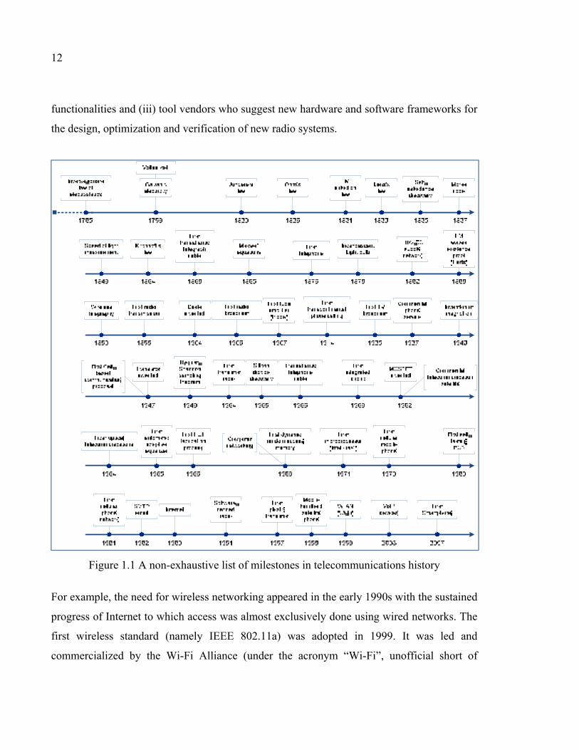
12
functionalities and (iii) tool vendors who suggest new hardware and software frameworks for
the design, optimization and verification of new radio systems.
Figure 1.1 A non-exhaustive list of milestones in telecommunications history
For example, the need for wireless networking appeared in the early 1990s with the sustained
progress of Internet to which access was almost exclusively done using wired networks. The
first wireless standard (namely IEEE 802.11a) was adopted in 1999. It was led and
commercialized by the Wi-Fi Alliance (under the acronym “Wi-Fi”, unofficial short of
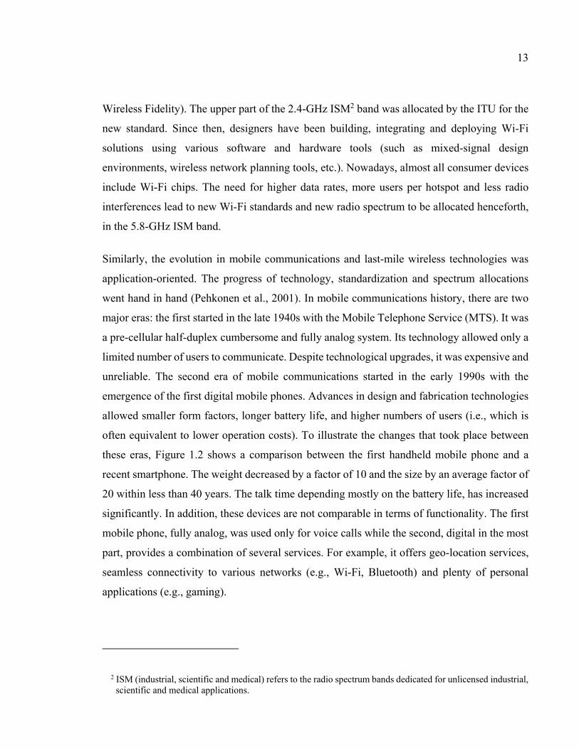
13
Wireless Fidelity). The upper part of the 2.4-GHz ISM2 band was allocated by the ITU for the
new standard. Since then, designers have been building, integrating and deploying Wi-Fi
solutions using various software and hardware tools (such as mixed-signal design
environments, wireless network planning tools, etc.). Nowadays, almost all consumer devices
include Wi-Fi chips. The need for higher data rates, more users per hotspot and less radio
interferences lead to new Wi-Fi standards and new radio spectrum to be allocated henceforth,
in the 5.8-GHz ISM band.
Similarly, the evolution in mobile communications and last-mile wireless technologies was
application-oriented. The progress of technology, standardization and spectrum allocations
went hand in hand (Pehkonen et al., 2001). In mobile communications history, there are two
major eras: the first started in the late 1940s with the Mobile Telephone Service (MTS). It was
a pre-cellular half-duplex cumbersome and fully analog system. Its technology allowed only a
limited number of users to communicate. Despite technological upgrades, it was expensive and
unreliable. The second era of mobile communications started in the early 1990s with the
emergence of the first digital mobile phones. Advances in design and fabrication technologies
allowed smaller form factors, longer battery life, and higher numbers of users (i.e., which is
often equivalent to lower operation costs). To illustrate the changes that took place between
these eras, Figure 1.2 shows a comparison between the first handheld mobile phone and a
recent smartphone. The weight decreased by a factor of 10 and the size by an average factor of
20 within less than 40 years. The talk time depending mostly on the battery life, has increased
significantly. In addition, these devices are not comparable in terms of functionality. The first
mobile phone, fully analog, was used only for voice calls while the second, digital in the most
part, provides a combination of several services. For example, it offers geo-location services,
seamless connectivity to various networks (e.g., Wi-Fi, Bluetooth) and plenty of personal
applications (e.g., gaming).
2 ISM (industrial, scientific and medical) refers to the radio spectrum bands dedicated for unlicensed industrial, scientific and medical applications.
14
This remarkable evolution results from advances in circuit design, fabrication processes,
components miniaturization, power management techniques, etc. The transition from fully
analog to mixed-signal design (i.e., cohabitation between digital and analog/RF circuitry) has
allowed more flexibility and interoperability since digital integrated circuits can be controlled
by software. Several analog functionalities were moved to the digital domain which provided
valuable gains in area and power. However, despite this progress, the analog/RF part in a
mobile phone remains the most challenging.
Figure 1.2 A comparison between the first handheld mobile phone and a recent smartphone
Besides the technological advances in mobile radios, cellular-communication standards have
known a remarkable progress. This evolution was commonly subdivided into “generations”.
After the primitive mobile networks (also called 0G) and the first generation of analog mobile
15
networks in the 1980s, the second generation of mobile standards came with digital cell
phones. The Global System for Mobile Communications (GSM) is the most globally deployed
standards. At its beginnings, it allowed an average data rate of 13 kbps which was roughly
enough for a decent voice call. This standard was later augmented by successive upgrades to
enhance its quality of service (e.g., GPRS3, EDGE4). By the early 2000s, the third generation
of cellular-communication standards had emerged (e.g., the Universal Mobile
Telecommunications System, UMTS for short) offering better data rates (around 2 Mbps). This
was followed by several upgrades and extensions to enhance the data rate and provide IP-over-
the-air services (e.g., HSPA5, LTE6). The fourth generation brings with LTE-A (i.e., LTE
Advanced) higher downlink peak data rates that may reach 1 Gbps. In roughly two decades,
cellular-communication standards multiplied useful data rates by a factor of 105. This was
possible due to growing spectrum allocation. It is also due to adaptive signal processing and
robust digital design. Despite the fact that techniques such as diversity, amplifier linearization
and dynamic power control have contributed to make RF front-ends more suitable for higher
data rates, this part of the cell-phone remains the most refractory for progress due to multiple
reasons that will be detailed in the following sections.
Likewise, microwave backhaul systems as well as wireless last-mile and wireless local
networks have evolved on many levels. Technically speaking, they took part in the same
technologies either digital or RF/microwave used for cellular communications. New spectrum
3 GPRS (General Packet Radio Service) is an upgrade of GSM networks providing typical bit rates around 80 kbps.
4 EDGE (Enhanced Data Rates for GSM Evolution) is an upgrade of GSM networks which allowed bit rates up to 400 kbps depending on the used modulation.
5 HSPA (High-Speed Packet Access) is an extension of 3G mobile communication networks allowing bit rates up to 42 Mbps. It was followed by HSPA+ providing peak data rates up to 168 Mbps.
6 LTE (Long-Term Evolution) is a standard for high-speed data mobile communications.
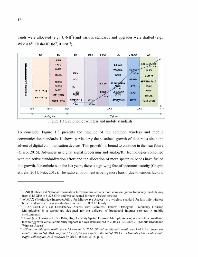
16
bands were allocated (e.g., U-NII7) and various standards and upgrades were drafted (e.g.,
WiMAX8, Flash-OFDM9, iBurst10).
Figure 1.3 Evolution of wireless and mobile standards
To conclude, Figure 1.3 presents the timeline of the common wireless and mobile
communication standards. It shows particularly the sustained growth of data rates since the
advent of digital communication devices. This growth11 is bound to continue in the near future
(Cisco, 2015). Advances in digital signal processing and analog/RF technologies combined
with the active standardization effort and the allocation of more spectrum bands have fueled
this growth. Nevertheless, in the last years, there is a growing fear of spectrum scarcity (Chapin
et Lehr, 2011; Petz, 2012). The radio environment is being more harsh (due to various factors:
7 U-NII (Unlicensed National Information Infrastructure) covers three non-contiguous frequency bands laying from 5.15 GHz to 5.825 GHz and was allocated for new wireless services.
8 WiMAX (Worldwide Interoperability for Microwave Access) is a wireless standard for last-mile wireless broadband access. It was standardized in the IEEE 802.16 family.
9 FLASH-OFDM (Fast Low-latency Access with Seamless Handoff Orthogonal Frequency Division Multiplexing) is a technology designed for the delivery of broadband Internet services in mobile environments.
10 iBurst (also known as HC-SDMA, High Capacity Spatial Division Multiple Access) is a wireless broadband technology with vehicular mobility support and was standardized in 2006 as IEEE 802.20 (Mobile Broadband Wireless Access).
11 “Global mobile data traffic grew 69 percent in 2014. Global mobile data traffic reached 2.5 exabytes per month at the end of 2014, up from 1.5 exabytes per month at the end of 2013. (…) Monthly global mobile data traffic will surpass 24.3 exabytes by 2019.” (Cisco, 2015, p. 1)
17
propagation conditions, growing interferences, etc.) which leads to tougher radio
specifications. In the light of these remarks, it becomes obvious that continuing this growth in
wireless and mobile communications will require the industry to face multiple challenges.
Consequently, what are the major trends in today’s industry and what solutions would be
adopted (on both technology and design levels) to tackle these challenges?
1.3 Future Trends in Wireless and Mobile Communications and Subsequent
Impact on Technology and Design Approaches and Tools
According to ITU, the Information and Communication Technology (ICT) market (including
mobile and wireless industry) is one of the most vibrant and dynamic markets worldwide (ITU,
2013). The prior success of wireless and mobile communications marked particularly by a
sustained growth of infrastructure and subscriptions is the key driver of this market. However,
this success may turn out to a major constraint since that the consumer is expecting higher
quality of service and better user experience at lower costs. It seems obvious that the key of
success in this field remains a good matching of market trends with relevant enabling
technologies in shorter timeframes. In this section, we attempt to examine this topic by
highlighting the trends in wireless and mobile communications and modestly assessing their
impact on technology and design approaches.
1.3.1 Trends in Wireless and Mobile Communications
The emergence of new applications and services has been a key driver of wireless and mobile
industry for decades. For instance, first mobile phones allowed voice calls only. Then, digital
technologies brought data services in addition to voice. The growing capabilities of digital
processing enabled multimedia applications and the progress of data rates allowed mobile
Internet. This evolution is bound to continue (Cisco, 2015). We discuss hereafter the future
trends in wireless and mobile communications from three different angles: user demands,
regulatory and standardization frameworks and enabling technologies.
18
a) User-driven trends and market shift
Network operators are working to provide consumers with better user experience (Nortel,
2008). This includes the provision of higher data rates, enhanced mobility, improved security
and better support of diverse application and traffic types (Costa-Perez et al., 2013). This effort
results in increased number of subscriptions and a market shift. In fact, ITU estimates that the
mobile-broadband subscriptions increased by 21% between 2010 and 2013. It also expects the
cellular subscriptions to reach 6.84 billion by the end of 2013 (ITU, 2013). The increase in
mobile broadband subscriptions is expected to continue. The availability of broadband services
has led to the emergence of new services, applications and paradigms (e.g., machine-to-
machine communications, converged services, cloud services, over-the-top services like VoIP,
cooperative intelligent systems, etc.) (Costa-Perez et al., 2013; ITU, 2013). This evolution
outlines a market shift that requires the wireless and mobile industry to adapt its products to a
constantly changing operation environment at affordable costs. In this regard, one can
particularly think about the underlying technology issues related for example, to RF front-end
design and operation.
b) Regulatory, spectrum management and standardization trends
The growth of fixed and mobile broadband services requires more frequency bands but is
facing regulatory challenges. Most current spectrum management policies are administrative-
oriented (ITU, 2013). Being an increasingly scarce commodity, regulatory organizations
should change their policies for more efficient use of RF resources (ITU, 2013; Petz, 2012).
The spectrum should be market-oriented and its fragmentation should be minimized in order
to accommodate more mobile and wireless services. There is a tendency to foster this
standpoint (e.g., allocation of U-NII bands for wireless services, use of TV white spaces to
locally take part of spectrum fragmentation, etc.). Technically, the implementation of such
approaches requires advanced spectrum sensing and radio awareness techniques (e.g.,
cognitive radio). However, such techniques are still at infancy because of RF design limitations
19
especially in complex radio environments (e.g., Dynamic Frequency Selection12 for U-NII
bands in some countries) (Petz, 2012; Steenkiste et al., 2009).
Furthermore, regulatory issues become more challenging when it comes to global effort. Inter-
organization cooperation to ensure network / service convergence is required but not always
easy to concretize (Costa-Perez et al., 2013; MobileInfo; Nokia Siemens Networks, 2011). The
effort is mostly focus on the development of new standards. However, this does not fully
resolve all the issues.
c) Core technology and network infrastructure trends
During the last few years, consumers are moving to use mobile from fixed networks (Roman
Friedrich, 2006). The Cisco Visual Networking Index expects that mobile data traffic will grow
at a 66% CAGR13 from 2012–2017 which is three times faster than the growth of global IP
fixed traffic during the same period (Cisco, 2013). With this sustained increase of fixed and
mobile data traffic, communication networks will continue to grow in terms of infrastructure
and capacity (Costa-Perez et al., 2013). Furthermore, the emergence of new applications and
the growth of mobile traffic are imposing two major trends. The first is the convergence of
different technologies and services. It aims to provide end users with a complementary set of
services independently from the network. For example, one can use seamlessly a fixed
wired/wireless, a mobile network or both for a voice call (e.g., the Unlicensed Mobile
Access14). The second trend is the migration to all-IP networks (Markova, 2009; Nortel, 2008).
To face this sustained growth and remarkable changes in networks, the wireless and mobile
industry is facing at least two challenges. The first is related to the core technology
12 Dynamic Frequency Selection (DFS) is a mechanism elaborated to allow unlicensed radios to use the 5-GHz frequency bands initially allocated for some radar systems. To avoid interference, DFS imposes to unlicensed radios the sensing of radio environment and the detection of radar presence before actually starting to communicate. Briggs, Mark. 2010. « Dynamic Frequency Selection (DFS) and the 5-GHz Unlicensed Band ».
13 CAGR (Compound Annual Growth Rate) is the geometric mean of year-over-year growth rate. 14 The Unlicensed Mobile Access (UMA) is a technology that allows seamless access to GSM, GPRS and
EDGE mobile services using unlicensed spectrum technologies such as Wi-Fi and Bluetooth. Yan Zhang, Laurence T. Yang, Jianhua Ma. 2008. Unlicensed Mobile Access Technology: Protocols, Architectures, Security, Standards and Applications. CRC Press.
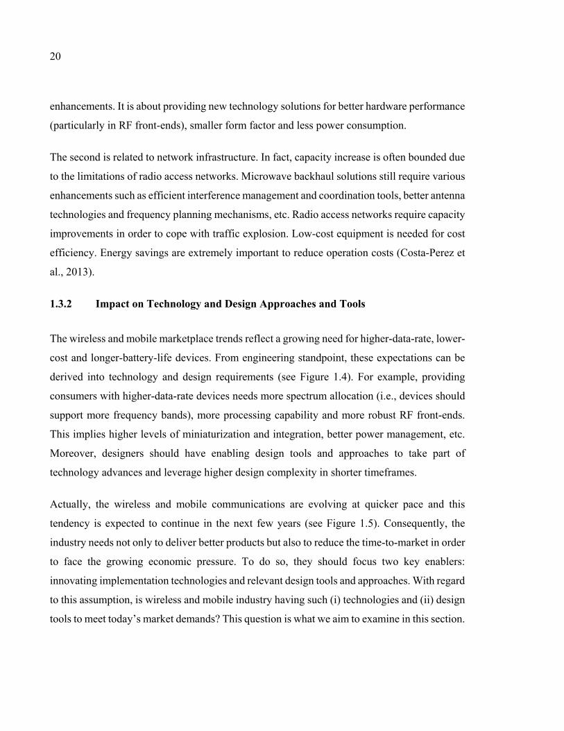
20
enhancements. It is about providing new technology solutions for better hardware performance
(particularly in RF front-ends), smaller form factor and less power consumption.
The second is related to network infrastructure. In fact, capacity increase is often bounded due
to the limitations of radio access networks. Microwave backhaul solutions still require various
enhancements such as efficient interference management and coordination tools, better antenna
technologies and frequency planning mechanisms, etc. Radio access networks require capacity
improvements in order to cope with traffic explosion. Low-cost equipment is needed for cost
efficiency. Energy savings are extremely important to reduce operation costs (Costa-Perez et
al., 2013).
1.3.2 Impact on Technology and Design Approaches and Tools
The wireless and mobile marketplace trends reflect a growing need for higher-data-rate, lower-
cost and longer-battery-life devices. From engineering standpoint, these expectations can be
derived into technology and design requirements (see Figure 1.4). For example, providing
consumers with higher-data-rate devices needs more spectrum allocation (i.e., devices should
support more frequency bands), more processing capability and more robust RF front-ends.
This implies higher levels of miniaturization and integration, better power management, etc.
Moreover, designers should have enabling design tools and approaches to take part of
technology advances and leverage higher design complexity in shorter timeframes.
Actually, the wireless and mobile communications are evolving at quicker pace and this
tendency is expected to continue in the next few years (see Figure 1.5). Consequently, the
industry needs not only to deliver better products but also to reduce the time-to-market in order
to face the growing economic pressure. To do so, they should focus two key enablers:
innovating implementation technologies and relevant design tools and approaches. With regard
to this assumption, is wireless and mobile industry having such (i) technologies and (ii) design
tools to meet today’s market demands? This question is what we aim to examine in this section.
21
a) Technology
Nowadays, most modern consumer wireless devices (and mobile phones) provide connectivity
to various communication networks. They are implemented as multi-standard, multi-band and
multi-mode transceivers. A similar handset is composed of three main parts (see Figure 1.6
and Figure 1.7). The first is the baseband block which consists of various application-specific
integrated circuit (ASIC) in charge of baseband signal processing. The second is the RF front-
end which is composed of a set of RF devices (e.g., filters, amplifiers, oscillators, etc.) used
for radio communications. In addition to all these components, generic processors, memory
chips and dedicated components (e.g., sensors, cameras, etc.) are dedicated for user
applications (e.g., video capture, gaming, etc.) and system management (e.g., operating system,
power control, data storage, etc.).
Figure 1.4 User expectations can be derived into technology and design requirements
If the wireless and mobile industry is currently able to deliver relatively satisfactory handsets,
there are however various challenges to address at different levels in order to cope with the
emerging demands:
22
1. Hardware performance
Hardware performance (in terms of either baseband processing capability or RF/analog
robustness) is becoming more critical than ever. In addition to user applications, increasingly
harsh radio environment (e.g., multipath, fading and interferers), spectrum crowdedness and
inherent radio impairments (e.g., nonlinearities) require more signal processing capability and
RF front-end reliability. Furthermore, to ensure good hardware performance, the handset
should have an excellent sensitivity in reception while in transmission, it should be able to
select the best configuration that maximizes the quality of service and optimizes the usage of
its resources (especially battery charge). Current radio systems suffer from various
shortcomings particularly at the RF front-end level. For instance, LTE smartphones are
hampered by fundamental limitations in the RF front-end that cannot be overcome with
traditional RF technology (Gianesello, 2012; Mobile Europe, 2012). Power amplification is
typically an outstanding issue in such handsets. Apple iPhone 5 does not support all frequency
bands because there is neither sufficient transmission power nor enough board space to
accommodate all the required power amplifiers (Gianesello, 2012; Mobile Europe, 2012).
To address all these issues, some innovative techniques are emerging. Efficient CMOS as well
as switched-mode power amplifiers may be suitable for chip integration and low-consumption
handsets (Andrew, 2011; Gianesello, 2012; Mobile Europe, 2012). Cognitive radio addresses
the issues related to the shortages/crowdedness of the spectrum. To increase the data rate,
diversity techniques may also help (e.g., Multi-Input/Multi-Output or MIMO).
2. Device’s complexity and form factor
At system level, the count of functional blocks in a typical handset is relatively limited
compared to devices in use few decades ago. In fact, the number of components on a mobile
phone board was about 300 in 1999 and around 100 in 2002 (Pulsford, 2002). Over the years,
this continuous reduction of components’ count (especially discrete passives) has contributed
to significantly reduce devices’ form factor (see Figure 1.5). Nevertheless, in the last years, the
form factor of wireless and mobile devices is slightly growing after it reached a minimum at
the early 2000s. There are two reasons for this. On the one hand, the emergence of mobile
23
Internet and gaming requires handsets with larger screens and better resolutions15. On the other
hand, serious limitations in the RF front-end (e.g., no broadband antennas) caused the
duplication of RF circuitry. In most cases, each supported communication standard has its
dedicated baseband and RF/microwave circuitry (this is depicted in Figure 1.6 and Figure 1.7).
On the baseband level, the reduction of the form factor comes at the cost of higher complexity.
But this is possible due to sophisticated design tools and technology maturity. For instance,
Figure 1.8 shows an ASIC chip that implements five communication standards. This chip
recently used in Apple iPhone 5 replaces at least three chips that were previously integrated
within Apple iPhone 4. In RF and microwave side, reducing the form factor of RF/microwave
components is difficult because it is limited by the laws of physics (e.g., electrical length).
However, numerous promising solutions are being tested. Among them, the use of Micro-
electromechanical Systems (MEMS) seems encouraging for both miniaturization and
reconfigurability. In addition, broadband and compact antennas can be achieved using
advanced tunable antennas. There is also a tendency to export bandwidth problems from RF to
digital domains. In this regard, software-defined radio is a good candidate particularly with the
notable advances in analog-to-digital and digital-to-analog converters.
3. Miniaturization and integration
A baseband integrated circuit (IC) contains hundreds of millions of devices combined in a very
small silicon area. The component count increases while the fabrication process minimum
feature size continues to decrease (see Figure 1.5). Nevertheless, a typical RF board contains
few dozens of components that are often cumbersome and power consuming. Paradoxically, it
is easier to integrate millions of digital components rather than a handful of RF/microwave
devices.
15 Between 2000 and 2010, the average display size of a handset has increased by approximately 60%. Korhonen, Kaisa. 2011. « Predicting Mobile Device Battery Life ». Aalto University, Finland.

24
There are various reasons behind this situation:
− Digital ICs are integrated using the same technology (i.e., CMOS16) while RF designers
use a mix of technologies (some RF devices such as duplexers, switches and power
amplifiers are off-chip and cannot be integrated within the same substrate (Hansen, 2003));
− Digital fabrication processes shrink down faster than it occurs in the analog and
RF/microwave side;
− Passive and discrete components represent more than 80% of the chip area (Pulsford,
2002). The use of passives is cheap and provides good performance but these components
are difficult to miniaturize and integrate. Reducing the subsequent area penalty is a
significant headache for designers.
Achieving more integration allows the implementation of more functionalities but is often
related to the increase of noise, parasitic effects and cross-talks. This is particularly true in the
case of mixed-signal design where digital and analog circuitry is combined in the same chip
(Ferragina et al., 2005; Masoumi et al., 2001). Digital circuits typically create noise that
interferes with analog circuitry performances. Packaging is another challenge to cope with due
to the heat dissipation issues that occurs due to higher density.
Hopefully, new integration techniques are emerging to tackle these issues. For example,
technologies such as High-Temperature/Low-Temperature Co-fired Ceramic (HTCC/LTCC)
allow effective multi-layer integration. System-on-Chip (SoC) is considered an efficient
solution for heat dissipation and may be prevalent in the design of future radios (Nokia Siemens
Networks, 2011). The Post-Silicon Tuning (PST) was thought to enhance the reliability and
robustness of ICs by minimizing the mismatches and parasitic effects due to process scaling
(Li et al., 2007).
16 CMOS (Complementary Metal-Oxide-Semiconductor) is a technology for the implementation of both digital and analog integrated circuits. Its major advantages are the low-static power consumption and good immunity to noise.
25
4. Power consumption and energy efficiency
Transmitting less power in wireless and mobile communications means longer battery life for
handheld devices, less inband blockers for other users and less power consumption for base-
stations. At the side of end-user, a significant proportion of the battery charge is consumed by
the RF front-end (and especially the power amplifier). Approximately, 30 to 40% of the battery
charge is consumed by the RF front-end against 20% by the baseband processors (Irmer et
Chia, 2009). According to (Hubbard, 2012), the average consumption of baseband processors
in smartphones has doubled between 2009 and 2011 while the RF front-end consumes 11%
more energy in 2011 than it was in 2009. Referring to the number of devices in a baseband
processor and a RF front-end, the power consumption per device has grown less in the former
than the latter.
Besides, the duplication of RF components in current multi-standard handsets does not only
increase the device’s form factor (i.e., the required board area increases) but also raises its
power consumption and degrades its performance (i.e., isolation, insertion loss, noise and heat
dissipation become critical design issues). Furthermore, the battery charge capacity did not
grow significantly in the last decades. For instance, the charge of Lithium-ion batteries (i.e.,
the most used battery type in modern handsets) increased by a factor of three in 15 years (see
Figure 1.5) while the average handset power consumption almost doubled in only two years
(Hubbard, 2012). The gap between the amount of energy required for a handset and the
available battery charge has been growing (Korhonen, 2011; Micallef, 2013).
At the operator side, cellular networks represent over 90% of ICT sector energy consumption.
Specifically, the power consumption of base-stations accounts for around 75% of the overall
network energy consumption (Guo, 2011). In addition to its environmental effects17, the
17 The estimates indicate that the ICT sector is responsible for 2 to 4% of the global carbon emissions. The power consumption related to network and equipment operation counts for 40 to 60% of this volume, which is bound to double by 2020. Vereecken, W., W. Van Heddeghem, M. Deruyck, B. Puype, B. Lannoo, W. Joseph, D. Colle, L. Martens et P. Demeester. 2011. « Power Consumption in Telecommunication Networks: Overview and Reduction Strategies ». Ieee Communications Magazine, vol. 49, no 6, p. 62-69.
26
subsequent economic impact18 is significant. For operators, the least power the network
consumes the least money they pay for the energy bill19 (Micallef, 2013).
Accordingly, reducing power consumption and developing more energy-efficient RF front-
ends allow an extended talk time for battery-powered handsets and lower operation costs for
network operators. To achieve that goal, most of efforts were focalized on improving power
amplifiers efficiency. This technique has proven until recently substantial gains. In recent
smartphones, a rule of thumb indicates that a 1% improvement in power amplifier’s efficiency
results in approximately 35 mAh gain in battery charge and around 50mm2 reduction in the
device’s form factor (Hubbard, 2012). At this regard, recent low-consumption reduced-noise
technologies (e.g., high-voltage GaAs HBT20 and GaN substrates) may be used to fabricate not
only power amplifier but also other energy-hungry RF components (e.g., oscillator, switch,
etc.) (Andrew, 2011; Ashbaugh, 2009; Lidow, 2013).
b) Design Approaches and Tools
Keeping pace with the market demands includes the enhancement of not only technologies but
also the design process of wireless and mobile handsets. This process covers various design
tasks such as analysis, implementation, integration and verification of both baseband and
analog/RF blocks. In each step of the design process, designers use software and/or hardware
tools in order to achieve various design tasks.
For analysis, designers need system-level tools to enhance design space exploration. This
implies the availability of high-level models for all involved components. Implementation
requires continuous update of technology libraries. It needs also tools for effective system
partitioning in order to easily derive the specifications of the functionalities to be designed and
18 The energy cost incurred by fixed and mobile network operators are 30% and 90% respectively. Koutitas, George, et Panagiotis Demestichas. 2010. « A review of energy efficiency in telecommunication networks ». Telfor journal, vol. 2, no 1, p. 2-7.
19 Emerging technologies allow energy cost savings up to 20%. Lange, C., D. Kosiankowski, A. Betker, H. Simon, N. Bayer, D. von Hugo, H. Lehmann et A. Gladisch. 2014. « Energy Efficiency of Load-Adaptively Operated Telecommunication Networks ». Journal of Lightwave Technology, vol. 32, no 4, p. 571-590.
20 HBT stands for “Hetero-junction Bipolar Transistor” which is a type of bipolar junction transistor. It can handle signals with frequencies up to several hundreds of GHz.
27
implemented separately. In addition to yield and performance optimization tools currently in
use, designers need at this step new tools for power estimation and form factor optimization.
Next, system integration allows the assembly of the various digital, analog and RF subsystems.
In this step, designers need a myriad of tools for floorplanning, placement and routing.
Finally, verification is an important step in the product design cycle. It aims to ensure that the
wireless and mobile device meets the initial specifications and delivers the intended
performance. Designers use numerous software and hardware tools to carry out design
verification and performance assessment. Regarding software tools, high-level and automated
tools assist digital designers with this time-consuming task (Wang, Chang et Cheng, 2009).
However, available tools for analog/RF designers are often limited (Berkley Design
Automation, 2009).
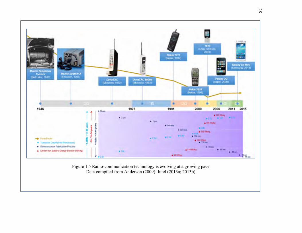
Figure 1.5 Radio-communication technology is evolving at a growing pace Data compiled from Anderson (2009); Intel (2013a; 2013b)
28
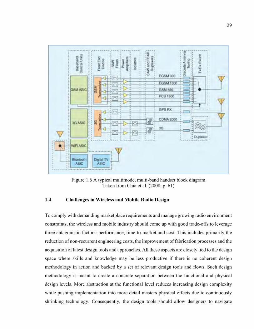
29
Figure 1.6 A typical multimode, multi-band handset block diagram Taken from Chia et al. (2008, p. 61)
1.4 Challenges in Wireless and Mobile Radio Design
To comply with demanding marketplace requirements and manage growing radio environment
constraints, the wireless and mobile industry should come up with good trade-offs to leverage
three antagonistic factors: performance, time-to-market and cost. This includes primarily the
reduction of non-recurrent engineering costs, the improvement of fabrication processes and the
acquisition of latest design tools and approaches. All these aspects are closely tied to the design
space where skills and knowledge may be less productive if there is no coherent design
methodology in action and backed by a set of relevant design tools and flows. Such design
methodology is meant to create a concrete separation between the functional and physical
design levels. More abstraction at the functional level reduces increasing design complexity
while pushing implementation into more detail masters physical effects due to continuously
shrinking technology. Consequently, the design tools should allow designers to navigate
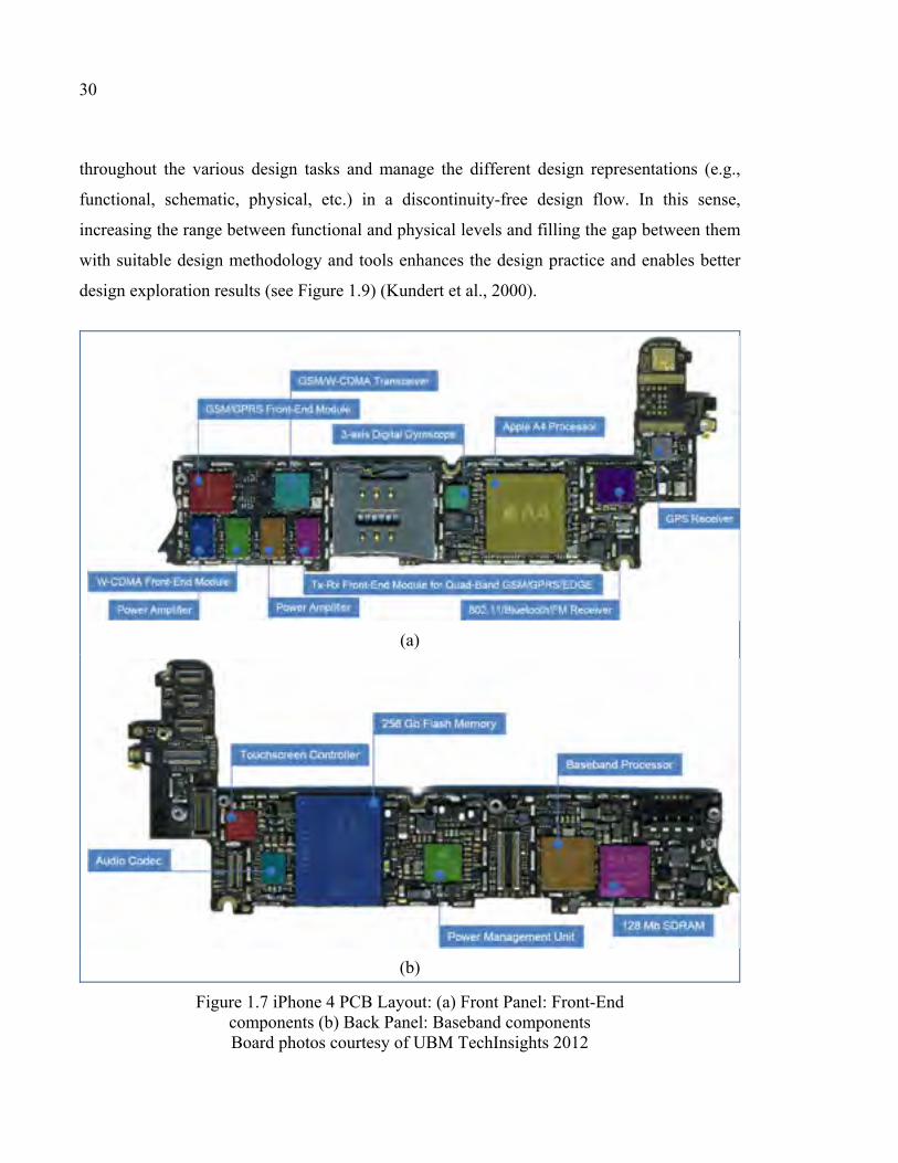
30
throughout the various design tasks and manage the different design representations (e.g.,
functional, schematic, physical, etc.) in a discontinuity-free design flow. In this sense,
increasing the range between functional and physical levels and filling the gap between them
with suitable design methodology and tools enhances the design practice and enables better
design exploration results (see Figure 1.9) (Kundert et al., 2000).
(a)
(b)
Figure 1.7 iPhone 4 PCB Layout: (a) Front Panel: Front-End components (b) Back Panel: Baseband components Board photos courtesy of UBM TechInsights 2012
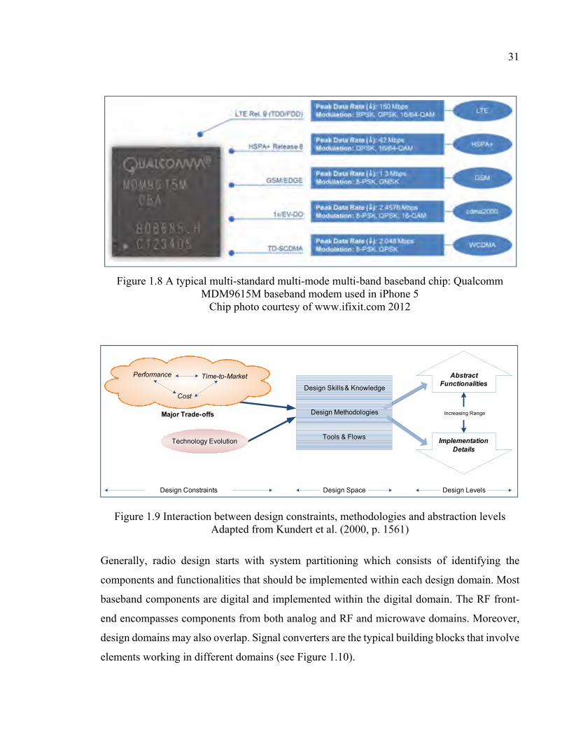
31
Figure 1.8 A typical multi-standard multi-mode multi-band baseband chip: Qualcomm MDM9615M baseband modem used in iPhone 5
Chip photo courtesy of www.ifixit.com 2012
Major Trade-offs
Technology Evolution
Performance
Cost
Time-to-Market
Design Skills & Knowledge
Design Methodologies
Tools & Flows Implementation Details
Abstract Functionalities
Increasing Range
Design LevelsDesign SpaceDesign Constraints
Figure 1.9 Interaction between design constraints, methodologies and abstraction levels Adapted from Kundert et al. (2000, p. 1561)
Generally, radio design starts with system partitioning which consists of identifying the
components and functionalities that should be implemented within each design domain. Most
baseband components are digital and implemented within the digital domain. The RF front-
end encompasses components from both analog and RF and microwave domains. Moreover,
design domains may also overlap. Signal converters are the typical building blocks that involve
elements working in different domains (see Figure 1.10).
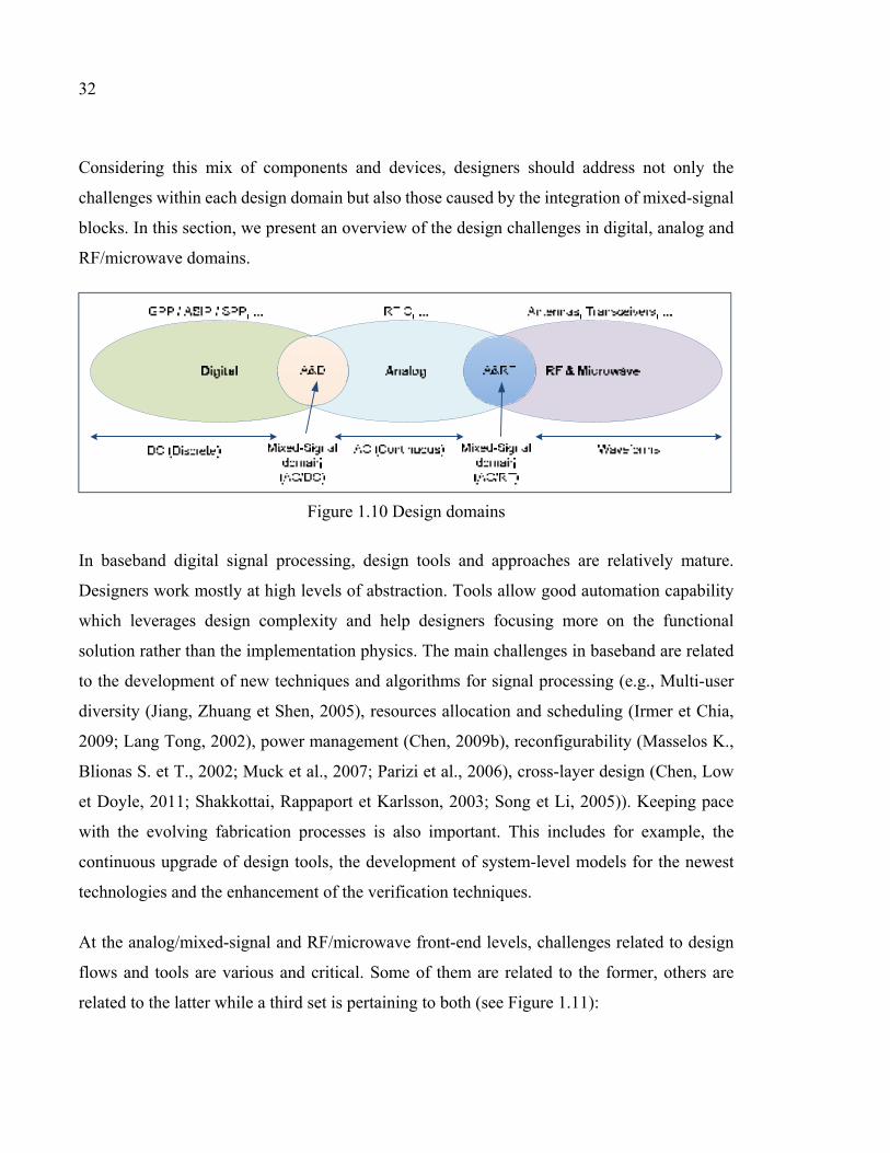
32
Considering this mix of components and devices, designers should address not only the
challenges within each design domain but also those caused by the integration of mixed-signal
blocks. In this section, we present an overview of the design challenges in digital, analog and
RF/microwave domains.
Figure 1.10 Design domains
In baseband digital signal processing, design tools and approaches are relatively mature.
Designers work mostly at high levels of abstraction. Tools allow good automation capability
which leverages design complexity and help designers focusing more on the functional
solution rather than the implementation physics. The main challenges in baseband are related
to the development of new techniques and algorithms for signal processing (e.g., Multi-user
diversity (Jiang, Zhuang et Shen, 2005), resources allocation and scheduling (Irmer et Chia,
2009; Lang Tong, 2002), power management (Chen, 2009b), reconfigurability (Masselos K.,
Blionas S. et T., 2002; Muck et al., 2007; Parizi et al., 2006), cross-layer design (Chen, Low
et Doyle, 2011; Shakkottai, Rappaport et Karlsson, 2003; Song et Li, 2005)). Keeping pace
with the evolving fabrication processes is also important. This includes for example, the
continuous upgrade of design tools, the development of system-level models for the newest
technologies and the enhancement of the verification techniques.
At the analog/mixed-signal and RF/microwave front-end levels, challenges related to design
flows and tools are various and critical. Some of them are related to the former, others are
related to the latter while a third set is pertaining to both (see Figure 1.11):
33
a) Design flows
Analog/mixed-signal and RF/microwave technologies have significantly evolved during the
last decades. However, most designers still start building RF front-ends at the circuit level.
This traditional approach was effective in the past because RF circuits and technologies were
relatively simple. However, today there is a common consensus that RF designers lack
effective design flows to overcome the growing complexity of RF circuits (Chang et Kundert,
2007; Iniewski, 2007). At this regard, various issues should be resolved:
− Technology dependence: RF designers deal with high frequencies. This requires multiple
design skills and exposure to a wide variety of different technologies at the same time. The
absence of effective system-level models pushes designers to work with circuit-level
models that makes technology the actual guide for the design. This absence of higher levels
of abstraction hinders the effort of design space exploration, reduces automation capability
and limits design reuse;
− Completeness: There is a lack of complete design flows for numerous RF/microwave
fabrication processes (e.g., SiP integration). This incompleteness is marked especially by
the absence of relevant design tools to accomplish various design tasks;
− Design concurrency: Most of RF/microwave designers still start building their systems at
the circuit level. That is a bottom-up design approach where tasks are carried out serially.
In this approach, the design time cannot be reduced by applying design concurrency.
Furthermore, there are no formal techniques or specialized tools to interface between
design stages. This is commonly done manually which increases design flaws and errors
that may be prohibitively expensive in time and money (particularly at the end of the design
cycle);
− Design collaboration: Starting design at the circuit level causes discontinuities in the design
cycle. In addition, designers tend to work in isolation from each other and communication
is generally poor. This may cause design flaws that are time-consuming and expensive to
correct;
− Co-design: According to (Wang, Stroud et Touba, 2008), 80% of digital chips contain
analog/RF circuitry. Digital and analog/RF circuits are built and tested in different domains
(time and frequency domains respectively). There is a lack in co-design approaches that
34
allow the simultaneous interaction between digital and analog/RF designers (i.e., mixed-
signal design and verification);
− Cost and TTM: Poor communication between designers, manual interfacing between
design stages, absence of design and verification tools and limited design concurrency
cause design re-spins to correct errors. On the contrary to digital circuits which succeed a
first pass test, RF circuits require multiple passes which raises design costs and increase
time-to-market (Hansen, 2003).
b) Tools
Design tools are the cornerstone of every design process. Designers use these tools for the
implementation, verification and performance assessment of wireless and mobile systems.
Despite recent advances (Cheng et al., 2010), design tools currently in use in RF/microwave
design suffer from various lacks and limitations:
− Multi-technology support: RF designers require tools that support different process
technologies at different levels. These tools should provide the feature of simulating a mix
of technologies at system-level (Park, Hartung et Dudek, 2007);
− Specifications validation: On the contrary, to digital design, tools used in RF domain do
not include the feature of specifications validation due to the lack of executable models
(Warwick et Mulligan, 2005);
− Modeling accuracy: Most tools (especially those used in RFIC design) suffer from the lack
in modeling accuracy, which affects the design quality. For example, models used for
passives and substrates are poor because they do not include parasitic effects (Dunham et
al., 2003). Another example is MOSFET21 circuit simulation which still suffers from
linearity issues and noise inaccuracies due to the inappropriate modeling of MOS devices
(Andriana Voulkidou, Stylianos Siskos et Noulis, 2012);
− Functional and physical verification: This aims to detect any design defects and errors.
Functional-level verification attempts to test the conformity of the design to the initial
21 MOSFET (Metal-oxide-semiconductor field-effect transistor) denotes a family of transistors used for switching and power amplification.
35
specifications at system level while physical-level verification checks if there are any
circuit-level defects, violation to design rules, etc. Some studies state that more than the
half of the development time is nowadays dedicated to verification. Additionally, as
technology shrinks verification time increases (Foster, 2012). However, most analog/RF
tools lack features for functional-level verification while physical-level one depends
generally on tools and available technology libraries;
− Tool specialization: Due to the complexity of RF design, tools do what they are best at.
Specific technologies (e.g., Silicon-on-Insulator) require specialized tools rather than
generic solutions lacking enough accuracy and dedicated features for particular
technologies (McMahon, 2009);
− Simulation issues: Most tools suffer from three main problems: (i) lack of high-level
simulation of digital and RF blocks to determine the circuit specifications (ii) poor circuit-
level simulation accuracy of nonlinear circuits and (iii) lack of accurate computation of
some devices parameters (e.g., oscillator phase noise) (Leenaerts, Gielen et Rutenbar,
2001; Wambacq et al., 2001). For the first problem, the analysis of complex modulation
schemes at system level is still difficult to do and most simulation tools do not provide fast
and correct performance data (Leenaerts, Gielen et Rutenbar, 2001). Furthermore, RF
simulators work well with individual blocks but still work poorly on algorithmic-based
blocks and heterogeneous systems (e.g., digital, analog and RF) (Kundert, 2005). For the
second issue, the simulation of nonlinear devices (particularly in large-signal domain) in a
reasonable time and with enough accuracy is still a major challenge in RF design (Dutton,
1997; Hartin et Yu, 2006; Zhiping et al., 1999). Regarding the third issue, most simulation
tools provide little accurate estimates of some system-critical parameters such as phase
noise (Bizzarri, Brambilla et Gajani, 2011; Wambacq et al., 2001). In addition, simulation
tools capability is often surpassed. The multi-domain simulation is often done by co-
simulation where two or more tools are used to evaluate the design performance. For
instance, the integration of power amplifiers and voltage-controlled oscillators require co-
simulation in order to estimate the performance in both electric and electro-magnetic levels.
Co-simulation is often error-prone and time-consuming;
36
− Automation: RF design is costly and time-consuming for not only the frequent design spins
needed to complete a design but also because most design steps are manual. Little RF tools
provide automated design support;
− Tools interaction and design data: Most tools lack the ability to interact with other tools
particularly those providing a different type of analysis (e.g., electromagnetic filed solvers,
noise and cross-coupling analyzers) (Dunham et al., 2003). The ability of exchanging
models and design data between different tools of different vendors is generally limited.
Old file formats (often limited and not uniformly supported by all the tools) are in use to
export data and layouts;
− Versioning and design reuse: The lack of an incremental top-down design approach makes
versioning and design reuse very difficult to do (Saleh et al., 2003). This is particularly true
for RF domain where most tools do not include such ability.
In addition to software tools used in radio design, hardware tools are used to test the
manufactured system and measure its physical performance parameters. This step aims also to
validate its electrical behavior and unveil any malfunctions. Various test instruments are
available for digital and analog/RF designers. However, many challenges are still present with
in this area. In fact, correlation between digital/analog and RF signals is challenging and
critical for correct radio operation (Akretch, 2012). Although mixing RF circuitry and
digital/analog devices causes signal integrity issues, verification still takes place separately in
time-domain for digital designs and frequency-domain for analog/RF ones. In this regard, there
is a lack of cross-domain test and measurement tools that can be used for mixed-signal designs.
But, some advances have emerged in the last years (e.g., mixed-domain oscilloscope (Akretch,
2012)). Furthermore, the performance of test instruments should exceed the unit under test.
The accuracy requisites have increased because performance requirements of wireless and
mobile systems have significantly increased (Poole, 2013). This has led to the emergence of
small-form-factor, multi-application and high-speed test instruments. The use of
reconfigurable hardware, software-defined radio and new test techniques (I/Q
modulators/demodulators, direct-conversion receivers, etc.) as well as the massive use of
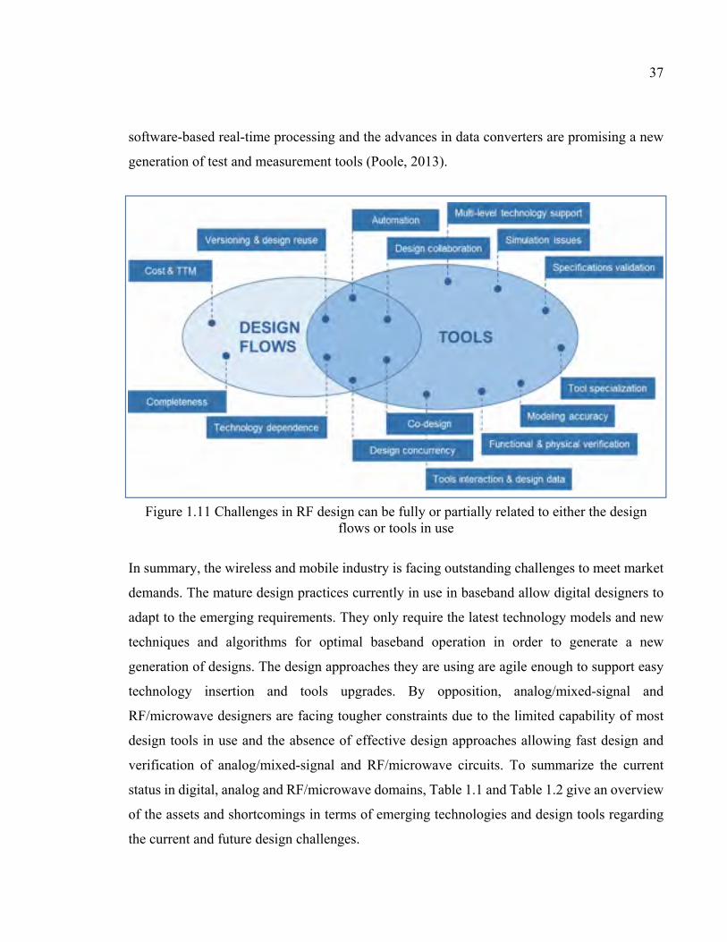
37
software-based real-time processing and the advances in data converters are promising a new
generation of test and measurement tools (Poole, 2013).
Figure 1.11 Challenges in RF design can be fully or partially related to either the design flows or tools in use
In summary, the wireless and mobile industry is facing outstanding challenges to meet market
demands. The mature design practices currently in use in baseband allow digital designers to
adapt to the emerging requirements. They only require the latest technology models and new
techniques and algorithms for optimal baseband operation in order to generate a new
generation of designs. The design approaches they are using are agile enough to support easy
technology insertion and tools upgrades. By opposition, analog/mixed-signal and
RF/microwave designers are facing tougher constraints due to the limited capability of most
design tools in use and the absence of effective design approaches allowing fast design and
verification of analog/mixed-signal and RF/microwave circuits. To summarize the current
status in digital, analog and RF/microwave domains, Table 1.1 and Table 1.2 give an overview
of the assets and shortcomings in terms of emerging technologies and design tools regarding
the current and future design challenges.
38
1.5 Conclusion
Radio communications have seen a tremendous evolution during the last two centuries. The
pace of this evolution was accelerated in the recent years due to the notable progress in
communication standards, advances in semiconductors as well as the advent of new design and
fabrication technologies. In this first chapter, we presented a historical perspective of this
evolution. We outlined the fact that technological developments, standardization efforts and
spectrum allocations were the basic mechanics that allowed the early radio communications to
evolve towards today’s wireless and mobile systems. Then, we presented the main trends
driving this evolution on the levels of market, technology and regulations. We concluded that
the success of wireless and mobile devices during the last decades is fueling the emerging
demands, especially in terms of QoS, cost and battery life. Next, we discussed the readiness of
the wireless and mobile industry and the impact of the increasingly tougher market demands
on current technologies and design tools.
In summary, this background review results in the following observations:
− Facing the emerging demands is not only bound to the evolution of technologies and
fabrication processes, it is also tied to the design approaches and tools in use;
− There is a clear and increasing gap between digital and analog/RF design, especially in
terms of tools and design flows;
− Even if the tools and design approaches currently used by digital designers are mature, this
may be difficult to maintain in the near future because of the convergence between digital
circuitry and analog/RF circuitry in the same device. Mixed-signal design tools either
hardware or software are not as advanced however;
− It becomes obvious that RF and microwave domains are lacking effective design
approaches and tools that are required to keep pace with market demands.
Most actors in both industry and academia focus on technological issues in their attempt to
meet the requirements of the next-generation wireless and mobile devices. Many efforts are
deployed to enhance power amplifiers efficiency, to broaden antenna bandwidth and reduce
nonlinearities, etc. The emphasis is mostly set on “what to do” but little interest is dedicated to

39
“how to do”. This first chapter highlighted the importance of radio design issues as well as the
need to address them along with emerging technology issues. The second chapter will look
closer and deeper at design methodologies and tools. The main purpose is to establish a
comparative study of the various design domains and summarize the pros and cons pertaining
to design practice within each of them.
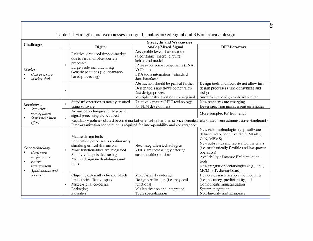
Table 1.1 Strengths and weaknesses in digital, analog/mixed-signal and RF/microwave design
Challenges Strengths and Weaknesses
Digital Analog/Mixed-Signal RF/Microwave
Market: Cost pressure Market shift
+
Relatively reduced time-to-market due to fast and robust design processes Large-scale manufacturing Generic solutions (i.e., software-based processing)
Acceptable level of abstraction (algorithmic, macro, circuit) + behavioral models IP reuse for some components (LNA, VCO, …) EDA tools integration + standard data interfaces
-
Abstraction should be pushed further Design tools and flows do not allow fast design process Multiple costly iterations are required
Design tools and flows do not allow fast design processes (time-consuming and risky) System-level design tools are limited
Regulatory: Spectrum
management Standardization
effort
+ Standard operation is mostly ensured using software
Relatively mature RFIC technology for FEM development
New standards are emerging Better spectrum management techniques
-
Advanced techniques for baseband signal processing are required
More complex RF front-ends
Regulatory policies should become market-oriented rather than service-oriented (elaborated from administrative standpoint) Inter-organization cooperation is required for interoperability and convergence
Core technology: Hardware
performance Power
management Applications and
services
+
Mature design tools Fabrication processes is continuously shrinking critical dimensions More functionalities are integrated Supply voltage is decreasing Mature design methodologies and tools
New integration technologies RFICs are increasingly offering customizable solutions
New radio technologies (e.g., software-defined radio, cognitive radio, MIMO, GaN, MEMS) New substrates and fabrication materials (i.e. mechanically flexible and low-power operation) Availability of mature EM simulation tools New integration technologies (e.g., SoC, MCM, SiP, die-on-board)
-
Chips are externally clocked which limits their effective speed Mixed-signal co-design Packaging Parasitics
Mixed-signal co-design Design verification (i.e., physical, functional) Miniaturization and integration Tools specialization
Devices characterization and modeling (i.e., accuracy, predictability, …) Components miniaturization System integration Non-linearity and harmonics
40
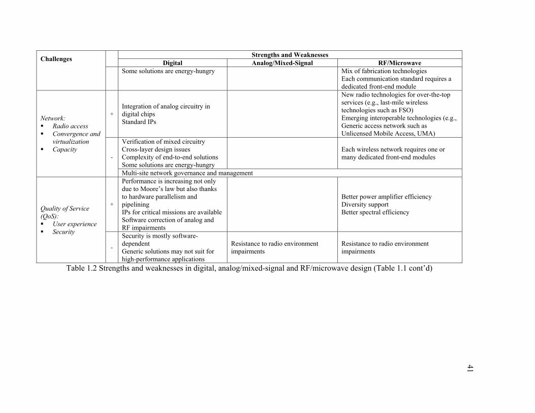
41
Challenges Strengths and Weaknesses
Digital Analog/Mixed-Signal RF/Microwave Some solutions are energy-hungry Mix of fabrication technologies
Each communication standard requires a dedicated front-end module
Network: Radio access Convergence and
virtualization Capacity
+ Integration of analog circuitry in digital chips Standard IPs
New radio technologies for over-the-top services (e.g., last-mile wireless technologies such as FSO) Emerging interoperable technologies (e.g., Generic access network such as Unlicensed Mobile Access, UMA)
-
Verification of mixed circuitry Cross-layer design issues Complexity of end-to-end solutions Some solutions are energy-hungry
Each wireless network requires one or many dedicated front-end modules
Multi-site network governance and management
Quality of Service (QoS): User experience Security
+
Performance is increasing not only due to Moore’s law but also thanks to hardware parallelism and pipelining IPs for critical missions are available Software correction of analog and RF impairments
Better power amplifier efficiency Diversity support Better spectral efficiency
-
Security is mostly software-dependent Generic solutions may not suit for high-performance applications
Resistance to radio environment impairments
Resistance to radio environment impairments
Table 1.2 Strengths and weaknesses in digital, analog/mixed-signal and RF/microwave design (Table 1.1 cont’d)
41

CHAPTER 2
COMPARATIVE STUDY OF COMMON DESIGN APPROACHES
2.1 Introduction
The growing success of wireless and mobile services resulted in the emergence of various radio
design challenges. To address them, new implementation and manufacturing technologies are
being developed. However, little interest is dedicated to how these technologies are put
together. Most designers focus more on technology solutions (i.e., “what-to-do”) rather than
which approaches and tools may be used to assemble these technologies (i.e., “how-to-do”) in
an optimal timeframe. This is particularly true in analog/RF design.
As discussed in the previous chapter, this tendency resulted in an increasing gap between
digital and analog/RF design practices. Added to the emerging need for relevant mixed-design
tools and approaches, the evolution of radio design depends henceforth not only on
technologies but also on available design frameworks. Consequently, the improvement of
design methodologies and tools becomes as important as the enhancement of implementation
technologies for future radio design.
The third chapter of this thesis presents a proposal of a new design framework for
RF/microwave circuits. Before doing so, we look closer and deeper at current design
approaches in the different domains related to radio design. Due to the relatively limited
literature documenting design methodologies particularly in RF/microwave domain, this
review aims to establish a strong understanding of design frameworks in use in the different
design domains. It also aims to elaborate a comparative study of these design approaches. The
goal is to identify and retain the best design practices as well as to identify their major
shortcomings.
We start this chapter by highlighting the traditional design approaches and the future
requirements in terms of design tools. Then, we review the design practice in digital,
44
analog/mixed-signal and RF/microwave domains. Finally, we present a comparative study of
their strength and weakness going forward.
2.2 Common Design Approaches and Future Requirements in Design Tools
Throughout the design process of a radio system, various digital, analog and RF/microwave
blocks are individually designed and tested. Depending on the available tools and the
fabrication technologies in use, designers may use diverse approaches to implement each radio
subsystem. Every approach is characterized by a given design flow. A design flow is a
combination of steps and tasks through which the radio system goes at each design stages (e.g.,
specifications, analysis, synthesis, validation, performance simulation, implementation,
verification and test, etc.). This design flow also determines the sequence in which these steps
are carried out as well as the design tools used in each stage. We present, in the following, an
overview of the common design approaches. We also highlight the tools requirements related
to future design practice.
2.2.1 Common Design Approches
Traditionally, there are two prevalent design approaches: bottom-up and top-down design
methodologies. Other approaches were also derived from one or both of them (e.g.,
performance/constraint-driven design).
a) Bottom-up design flow
The bottom-up design flow starts with the design of individual blocks that are assembled to
form a more complex block. These blocks are gradually combined to form the final system. In
practice, each individual block is implemented all the way to the lowest available abstraction
level (e.g., transistor-level in analog ICs) according to a set of specifications. Next, the block
is tested and verified separately. Finally, all blocks are gathered, assembled and verified
together. The entire system ends up generally with the lowest abstraction level representation
(Kundert, 2006). The bottom-up design flow is effective for small designs. However, as design
size increases, some integration and performance problems also appear (Kundert et Chang,
2005):
45
− After assembly, verification process is hard because simulations are time-consuming.
Errors found at system assembly are too difficult and expensive to fix. This situation may
cause delays in the project and requires several prototyping spins;
− Errors in communication between different designers may be critical once the system is
assembled;
− Expensive steps such as the system-level verification and test are performed serially. This
is coupled to a poor communication strategy between designers increases significantly the
design cost and time.
b) Top-down design flow
The top-down design flow starts with the whole system concept and then recursively breaks it
down into smaller pieces, easy to implement, test and validate. The design level at which this
approach starts is referred to as the system level (Frevert et al., 2006). At top-level, the
architecture is defined as a block diagram that is refined and optimized to meet the
specifications. The specifications of the underlying blocks are then derived from system-level
architecture simulation. Once all blocks and sub-blocks are individually designed and verified,
the overall system is assembled and verified against the original requirements.
This said; top-down design emerged to address the issue of performance degradation caused
by bottom-up design flows. It allows an architectural exploration step that figures out most
potential system solutions. However, it does not include efficient verification schemes. This
issue may stretch the design time and increase its cost due to unwanted but mandatory multiple
iterations. Furthermore, while top-down design enhances productivity by easing team work
and communication from upper to lower levels, this design approach may add discontinuities
in the design flow leading to blocks implementations that are incompatible with the system-
level architecture (Kundert et Chang, 2005). To address these issues, various changes were
proposed to improve the design approach. For instance, (Kundert, 2006) proposed a top-down
design and verification flow that systematically proceeds from the highest level (e.g., system-
level architecture) to the lowest-level (e.g., transistor-level representation) to a full verification
of each design level before moving upward or downward. This aims to reduce any design flaws
46
or incompatibilities and to improve the communication between designers, particularly those
located at different sites.
c) Comparison between bottom-up and top-down design flows
The bottom-up design methodology is mostly adopted by analog and RF/microwave designers
because they still start their design at the circuit level. On the contrary, the top-down design
approach is frequently adopted by digital designers because it is a hierarchical methodology
based on the “divide and conquer” concept. Each of the design approaches has its own
advantages and limitations. The main advantage of the bottom-up design approach is accuracy
of device characterization while its major shortcoming is complexity management. Similarly,
the top-down design approach is characterized by the effectiveness of design space exploration
while it generally suffers from verification process efficiency. Table 2.1 presents a comparison
between the two design approaches.
To take advantage of the strengths of both approaches, various mixes were proposed. For
example, (Frevert et al., 2006) proposed a hybrid design flow commonly known as the “V”
diagram, which combines a top-down design flow with a bottom-up verification process. The
top-down flow proceeds with the design from the system-level through the transistor-level
while the bottom-up verification process starts at the layout level and proceeds up to the highest
levels.
For performance-critical applications, the performance-driven design22 was proposed (Gielen
et Rutenbar, 2000). This approach consists of the alternation of a top-down flow, used in
design, and a bottom-up flow, used in verification at all design stages. At each level, the system
is subdivided into sub-blocks to be implemented (i.e., topology selection). These sub-blocks
are sized, optimized and verified against the performance specifications (i.e., specification
translation). Once the sub-blocks are assembled at the same level, the new assembly is verified
(i.e., layout generation and extraction). This approach ensures that the designed sub-blocks
meet always the performance constraints before going further in the design flow.
22 It is also called constraint-driven design approach.
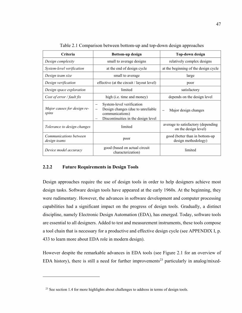
47
Table 2.1 Comparison between bottom-up and top-down design approaches
Criteria Bottom-up design Top-down design
Design complexity small to average designs relatively complex designs
System-level verification at the end of design cycle at the beginning of the design cycle
Design team size small to average large
Design verification effective (at the circuit / layout level) poor
Design space exploration limited satisfactory
Cost of error / fault fix high (i.e. time and money) depends on the design level
Major causes for design re-spins
− System-level verification − Design changes (due to unreliable
communications) − Discontinuities in the design level
− Major design changes
Tolerance to design changes limited average to satisfactory (depending
on the design level)
Communications between design teams
poor good (better than in bottom-up
design methodology)
Device model accuracy good (based on actual circuit
characterization) limited
2.2.2 Future Requirements in Design Tools
Design approaches require the use of design tools in order to help designers achieve most
design tasks. Software design tools have appeared at the early 1960s. At the beginning, they
were rudimentary. However, the advances in software development and computer processing
capabilities had a significant impact on the progress of design tools. Gradually, a distinct
discipline, namely Electronic Design Automation (EDA), has emerged. Today, software tools
are essential to all designers. Added to test and measurement instruments, these tools compose
a tool chain that is necessary for a productive and effective design cycle (see APPENDIX I, p.
433 to learn more about EDA role in modern design).
However despite the remarkable advances in EDA tools (see Figure 2.1 for an overview of
EDA history), there is still a need for further improvements23 particularly in analog/mixed-
23 See section 1.4 for more highlights about challenges to address in terms of design tools.
48
signal and RF/microwave design tools. The emerging challenges in radio design require a
robust and highly productive design tool chain. Accordingly, (Sangiovanni-Vincentelli, 2003)
estimates that future EDA tools should:
− Support design representations with rigorous semantics,
− Be able to tackle complex designs where various trade-offs should be considered,
− Concentrate multi-discipline engineering skills (e.g., microelectronic, RF, mechanical,
micro-electromechanical, environmental, etc.),
− Allow efficient collaboration between different design teams,
− Include more robust automated design validation/verification methods,
− Provide a central database that can handle design and manufacturing data throughout the
design cycle, and
− Provide more clear abstraction levels with flawless distinction between them (e.g. each
layer has its critical parameters) and define an efficient way to move from a layer to
another.
In summary, each design domain has its own needs in terms of tool requirements. Tools used
by digital designers are more mature than those used by their analog/RF counterparts. If digital
design tools should keep the same pace with the advances in technology, tools used in analog,
mixed-signal and RF/microwave design are expected to live major changes in order to be able
to alleviate various issues (e.g., design complexity, technology insertion, design automation,
etc.).
2.3 Lessons to be learned from Current Design Practice
The radio design involves the implementation, fabrication and testing of different blocks. Some
of them are digital (e.g., baseband processors), others are analog (e.g., signal converters) and
the remaining are RF/microwave (e.g., signal amplifiers). Most of these blocks are
implemented and verified separately before being integrated and tested in the phase of final
radio assembly. Different design approaches and tools are used to design and manufacture each
of these blocks. This reflects the differences between design practices in each design domains.
With the increasing need for smaller form factors along with more integrated functionalities,
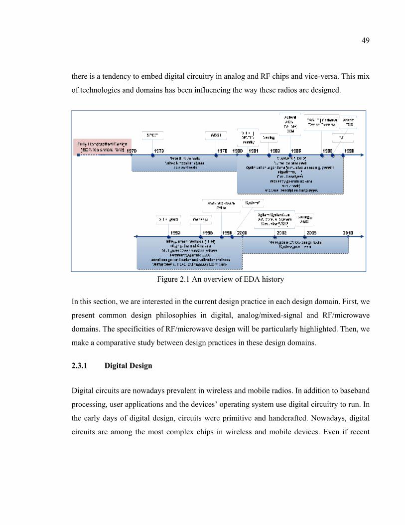
49
there is a tendency to embed digital circuitry in analog and RF chips and vice-versa. This mix
of technologies and domains has been influencing the way these radios are designed.
Figure 2.1 An overview of EDA history
In this section, we are interested in the current design practice in each design domain. First, we
present common design philosophies in digital, analog/mixed-signal and RF/microwave
domains. The specificities of RF/microwave design will be particularly highlighted. Then, we
make a comparative study between design practices in these design domains.
2.3.1 Digital Design
Digital circuits are nowadays prevalent in wireless and mobile radios. In addition to baseband
processing, user applications and the devices’ operating system use digital circuitry to run. In
the early days of digital design, circuits were primitive and handcrafted. Nowadays, digital
circuits are among the most complex chips in wireless and mobile devices. Even if recent
50
studies (e.g., (Chien et Karamcheti, 2013)) claim that the Moore’s law24 is reaching its limit, it
is expected that digital chips complexity will continue to rise in the next few years. Besides,
digital designers can leverage growing complexity thanks to the hierarchical design approach
they use and tool’s support of high abstraction levels.
A typical digital design flow consists of various design stages that start with specifications and
end with the packaged chip. The nomenclature of each step and the tasks to be undertaken in
each of them may vary in the industry due to different factors (e.g., tool vendors, involved
technologies, etc.). Hereafter, we present the common design stages (see Figure 2.2) to give a
global perspective of the top-down design approach used in digital design (Sherwani, 2012):
1. System Specification: the design process of a digital device/system starts with the
elaboration of its specifications. It represents the design entry. It gathers the requirements
and constraints that should be met by the final product. Specifications often include
performance indicators (e.g., speed), functionality details, and SWaP requirements.
Technology considerations (e.g., fabrication, design techniques) may be also defined in
specifications;
2. Functional/Architectural Design: depending on the system’s complexity, this step may be
subdivided into two consecutive design stages: architectural and functional. In the first one,
the basic architecture of the system is defined along with the corresponding specifications
(e.g., performance, SWaP, etc.). The resulting architecture presents the subsystems’ blocks
and how they are interconnected and/or meant to interact. The purpose of the functional
design is to identify the system’s functional units. Individual blocks specifications and their
interconnections to its environment are also defined. In both designs, a special attention is
given to the system’s behavioral aspects (in terms of architecture, inputs, outputs and
timing related to each unit). Behavioral models are used to provide a full description of the
system without specifying the internal structure of each unit or its implementation
24 Moore’s law is an empirical observation stated by Gordon E. Moore (Intel co-founder) in 1965 and expects the number of transistors on integrated circuits to double approximately every 12 months. Moore, Gordon E. 2006. « Cramming more components onto integrated circuits, Reprinted from Electronics, volume 38, number 8, April 19, 1965, pp. 114 ». IEEE Solid-State Circuits Newsletter, vol. 3, no 20, p. 33-35. This observation was later extended to other devices (e.g., memory).
51
technology. These models allow an early estimation of the system’s performance and the
detection of any structural/functional defects;
3. Logic Design: In this step, the internal structure and operation of each functional unit is
derived and tested. For example, the control flow, arithmetic and logic operations are
particularly verified. Hardware description languages (HDL) are commonly used to
provide a thorough description of each unit using Boolean expressions and relevant timing
information. The logic is simulated and verified to avoid design errors and ensure its
conformity to the functional design. Boolean optimizations can take place in order to
achieve smaller design. High-level synthesis tools may be used to automatically derive
design logic directly from behavioral models (i.e., functional/architectural levels);
4. Circuit Design: In this step, logic gates and Boolean expressions are converted into circuits.
Electrical components are carefully selected to meet performance and SWaP requirements.
Intensive circuit simulation is used to validate the timing response of circuits and ensure
the correctness of the design. The output of this step is a detailed diagram including all the
electrical elements (e.g., cells, transistors, lumped components, etc.) and the way they are
interconnected (i.e., netlist). Some EDA tools provide the capability of automatically
generating a circuit-level representation (including the schematic and the netlist) from the
logic description. This is commonly called logic synthesis;
5. Physical Design: the physical layout is generated from the circuit design in this step. The
netlist and the circuit components are converted into geometric shapes and represented
according to the process design rules. The geometric patterns express how exactly elements
should be physically implemented and interconnected. Fabrication materials and layers are
commonly color-coded. In physical design, designers focus particularly on how to place
the different functional blocks while minimizing the physical area (i.e., floorplanning).
They should take into account how these blocks should be interconnected without violating
design rules neither degrading the overall performance (i.e., place and route). Once these
tasks are accomplished, an operation called “Layout versus Schematic” (LVS) begins. It
consists of extracting a new schematic from the implemented layout and comparing it to
the original one to ensure design correctness. This operation takes place jointly with
another one, namely “Design Rule Check” (DCR), which checks whether the physical
52
layout meets the process design guidelines (e.g., maximum allowed spacing between
objects, etc.). Physical design is a very complex and labor-intensive stage. It encompasses
various validation and verification tasks to ensure that the layout is correct. Some EDA
tools enable either automated or semi-automated generation of the layout directly from
logic (i.e., Layout synthesis). The productivity gain from automation is generally acquired
at the price of some penalties (e.g., additional silicon area and performance degradation).
Thus, performance and area-sensitive designs are mostly manually optimized to address
the automatic layout synthesis limitations;
6. Fabrication: after layout optimization and verification, the design is exported as a data file
(e.g., Gerber25, GDSII26, etc.) and used to generate a photolithographic mask for each
physical layer of the chip. These masks are used during the fabrication process to identify
which materials should be deposited on the wafer and what areas should be etched. The
fabrication process requires sophisticated tools and skills to produce defect-void chips.
Before launching large-scale chip production, some prototypes are manufactured and
carefully tested;
7. Packaging: the design is manufactured on a wafer of several chips. The chips are then
separated and tested to ensure that they meet the initial specifications. Finally, chips
intended to be used on PCBs are packaged using various mounting technologies (e.g., Pin
Grid Array (PGA) and Ball Grid Array (BGA)). However, those used in multi-chip
modules (MCMs) are not packaged.
25 Gerber is an open file format used as a de facto industry standard for the description and exchange of PCB structures.
26 GDSII (short of Graphic Design System II) is a database file format used to exchange integrated circuits artworks.
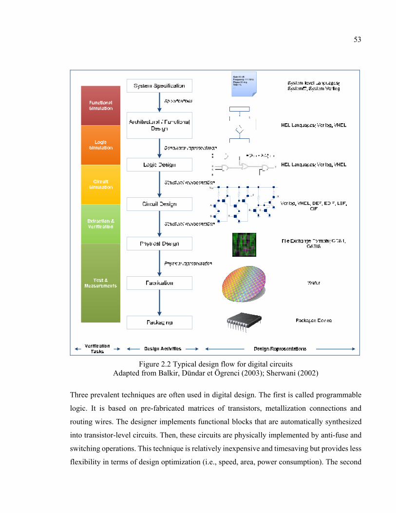
53
Gain 60 dBFrequency 111 MHzPhase 60 deg.THD 1%…
VDD
A
B X
CB
XF
Figure 2.2 Typical design flow for digital circuits Adapted from Balkir, Dündar et Ögrenci (2003); Sherwani (2002)
Three prevalent techniques are often used in digital design. The first is called programmable
logic. It is based on pre-fabricated matrices of transistors, metallization connections and
routing wires. The designer implements functional blocks that are automatically synthesized
into transistor-level circuits. Then, these circuits are physically implemented by anti-fuse and
switching operations. This technique is relatively inexpensive and timesaving but provides less
flexibility in terms of design optimization (i.e., speed, area, power consumption). The second
54
technique is called full-custom design. It consists of designing all the functionalities from the
scratch. This results in a highly optimized performance and reduced area device but also a
costly, labor-intensive and time-consuming design cycle. To accommodate moderate-
requirement applications, a third technique, namely semicustom design, is used. It consists of
using ready-to-use well-designed functional blocks (i.e., standard cells) and focus on building
efficient interconnections between them instead of building all the functionalities from the
ground up. This reduces design time and cost and provides devices with good performance
(Chen, 2009a).
Digital designers have succeeded in handling increasing design complexity due to the design
approach they adopted during the last decades. This approach, namely hierarchical design, is
an incremental “divide and conquer” process that is amenable for automation. In this approach,
a circuit is considered as a collection of modules. Each module is a collection of sub-blocks
(commonly designated as cells). Each sub-block implements a given functionality that can be
reused as much as required. Thus, the design effort is reduced. This design fashion is enabled
by a core concept in digital design: hardware abstraction27(Rabaey, Chandrakasan et Nikolic,
2002). To understand how important this concept, let us go back to the circuit-level where
designers deal almost exclusively with electrical models of components. It is all about a
physical representation of the device. In very complex designs, one cannot manage the
parameters of millions of transistors at the same time. To avoid this issue, logical blocks were
created to represent collections of circuits. The functionality of each logical block is defined
using Boolean equations. That is a structural representation. However, with the sustained
increase of design complexity, this representation became limited. For this reason, behavioral
representation was presented. It consists of a high-level description of both device’s structure
and behavior. The device’s structure consists of defining the immediate composing modules
(e.g., interfaces) while the behavioral description defines the interaction between them (e.g.,
timing, operations schedule, etc.). Hardware description languages (e.g., VHDL, Verilog) are
used to carry out this high-level description (see Figure 2.2). Thus, increasing the abstraction
27 The concept of “hardware abstraction” is developed in section 4.2 of chapter 4.
55
level masks the complexity of the underlying blocks without sacrificing the accuracy of their
actual response.
In summary, the main advantages of this hierarchy of abstraction levels are complexity
reduction, design automation and reuse (Rabaey, Chandrakasan et Nikolic, 2002). In fact, at
each abstraction level, the designer deals only with the models available at that level. Given
enough data about their functionality, the designer can use these models without knowing their
internal structure. The characteristics of their underlying components are virtually masked.
Complexity is thus reduced and mastered. Moreover, logical functionalities can be easily
derived from behavioral models. Similarly, they can also be transformed easily into physical
circuits (given relevant technology inputs). Then, it is possible to automate the transition
between all these abstraction levels. In addition, hardware abstraction results in modular
functionalities, arranged as simple as possible. They are thought to encompass fine
characterization at local level and provide a regular behavior and modular structure at system
level. All this enables the easy reuse of them in future designs without significant changes.
This said, digital designers face various challenges particularly in full-custom designs where a
relatively considerable workforce is involved. For example, design partitioning which consists
in breaking up the chip into small units that can be implemented separately by different teams
is sometimes a major design management issue. If this partitioning is successful, it results in
substantial time and cost reduction. Nevertheless, if it fails, this may enlarge the design
process. The management of specifications and design changes especially during the latest
phases of design cycle is also challenging. The exchange of design data throughout the
different design stages is also important. Fortunately, the hierarchical design approach enabled
the development of mature design tools that can reduce the impact of these issues. Modern
tools were also developed to enhance design space exploration, automate most design tasks
and enable a repetitive validation process.
56
2.3.2 Analog and Mixed-Signal Design
By opposition to their digital counterparts, analog circuits handle continuous analog signals
whose frequency ranging from DC up to few hundreds of megahertz. Phase-locked loops
(PLL), operational amplifiers, active filters and some radiofrequency integrated circuits
(RFICs28) are examples of typical analog circuits.
Pure analog designs often use technologies where behavioral models are absent. Then,
designers start at circuit level. Specifications are commonly so generic, which makes the design
space exploration an important phase. Designers should make various trade-offs in order to
come up with an initial solution that may be optimized later. Next, it is derived into a circuit
whose topology is captured in a schematic (i.e., schematic capture). At this step, the designer
interconnects elementary elements (e.g., transistors, resistors, etc.) to build up the selected
topology. For each individual element in the schematic, its properties are specified (e.g.,
transistor width-to-length ratio). To reduce circuit complexity and make the circuit topology
more understandable for teammates, designers identify a bench of components that can build
individual functionalities and create a new symbol for them. This new symbol (i.e., module) is
a sort of “artificial black-box” having a number of inputs and outputs and virtually hiding the
underlying circuit details. This task is often repeated recursively. Nevertheless, higher levels
simulators unfold these “black boxes” in order to carry out a variety of simulations.
In the following, Figure 2.3 presents some key steps of the previously mentioned design
philosophy. This example depicts a bottom-up design flow using a commercial EDA
framework for analog and mixed-signal design (namely Cadence29). As shown in Figure 2.3,
the design starts with specifications describing the functionality and the requirements that the
final product should meet (e.g., area, power, delay, etc.). Then, the designer selects an initial
circuit topology that is captured in a schematic.
28 The term “radiofrequency (RF)” in RFIC indicates that this category of circuits is used in RF applications and commonly integrated on RF boards.
29 Cadence refers to a suite of EDA tools for analog and mixed-signal design that are developed and maintained by Cadence Design Systems Inc.
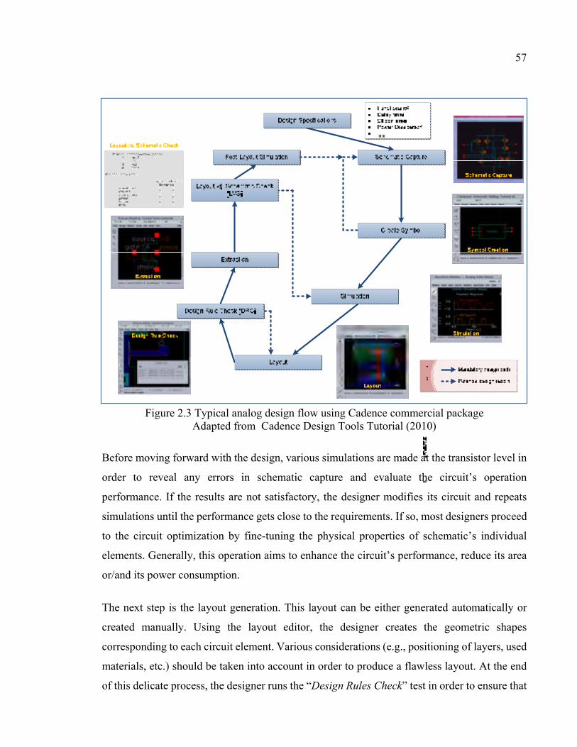
57
Figure 2.3 Typical analog design flow using Cadence commercial package Adapted from Cadence Design Tools Tutorial (2010)
Before moving forward with the design, various simulations are made at the transistor level in
order to reveal any errors in schematic capture and evaluate the circuit’s operation
performance. If the results are not satisfactory, the designer modifies its circuit and repeats
simulations until the performance gets close to the requirements. If so, most designers proceed
to the circuit optimization by fine-tuning the physical properties of schematic’s individual
elements. Generally, this operation aims to enhance the circuit’s performance, reduce its area
or/and its power consumption.
The next step is the layout generation. This layout can be either generated automatically or
created manually. Using the layout editor, the designer creates the geometric shapes
corresponding to each circuit element. Various considerations (e.g., positioning of layers, used
materials, etc.) should be taken into account in order to produce a flawless layout. At the end
of this delicate process, the designer runs the “Design Rules Check” test in order to ensure that
58
the layout does not violate the fabrication process guidelines. Cadence reports the eventual
errors to the designer who should modify the layout in order to resolve the detected issues.
Once the layout is completed, the designer uses a netlist extraction tool to obtain a realistic
representation of the device that takes into account the parasitic effects and other technology
considerations. Based on this netlist, the circuit simulation gives a good approximation of the
final device’s performance. This netlist is also used in the “Layout-versus-Schematic” test in
order to check if the extracted and the original netlists are equivalent. If so, the designer is
confident that the device’s layout matches with the schematic. However, this is not a guarantee
that the intended device’s performance is met. For this reason, the last step before
manufacturing is the post-layout simulation. It uses the generated layout and the extracted
netlist in order to assess the real performance of the device. This assessment takes into account
the parasitics and points out any critical glitches in the device.
As indicated in Figure 2.3 (see dashed lines), these steps are carried out iteratively in order to
correct design errors and optimize the device’s performance. The design is exported for
prototype manufacturing. After fabrication, the device is tested in realistic conditions to
evaluate its actual performance and whether it presents any defects.
Since the early 2000s, embedding analog circuitry in digital chips became an overwhelming
tendency. According to (Cadence Design Systems, 2002), it was expected that 40% of
developed wafers in 2002 were analog/mixed-signal. In 2006, (Rutenbar, 2006) states that 75%
of digital chips included analog content. Joining analog and digital circuitry on the same chip
has multiple advantages such as the integration of more functionality in reduced area and lower
costs.
The development of mixed-signal circuits has been carried out using silicon-based
technologies (e.g., BiCMOS, Bipolar, etc.) since digital and analog circuitry are integrated on
the same substrate. Silicon technologies allow good scaling capabilities which enabled the use
of digital-like design flows to develop embedded analog parts. Nonetheless, the difference in
nature between digital and analog circuits (e.g., digital blocks are noise-immune while analog
ones are very noise-sensitive) affected the abstraction hierarchy used for analog circuitry. For
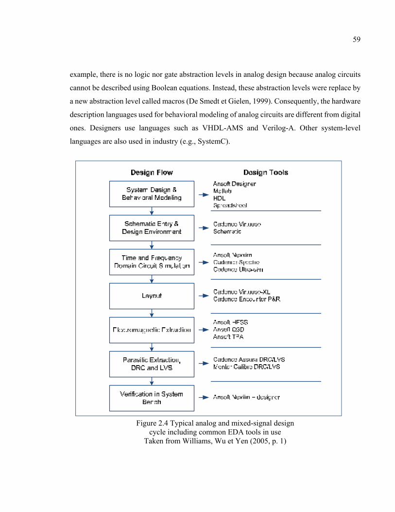
59
example, there is no logic nor gate abstraction levels in analog design because analog circuits
cannot be described using Boolean equations. Instead, these abstraction levels were replace by
a new abstraction level called macros (De Smedt et Gielen, 1999). Consequently, the hardware
description languages used for behavioral modeling of analog circuits are different from digital
ones. Designers use languages such as VHDL-AMS and Verilog-A. Other system-level
languages are also used in industry (e.g., SystemC).
Figure 2.4 Typical analog and mixed-signal design cycle including common EDA tools in use
Taken from Williams, Wu et Yen (2005, p. 1)
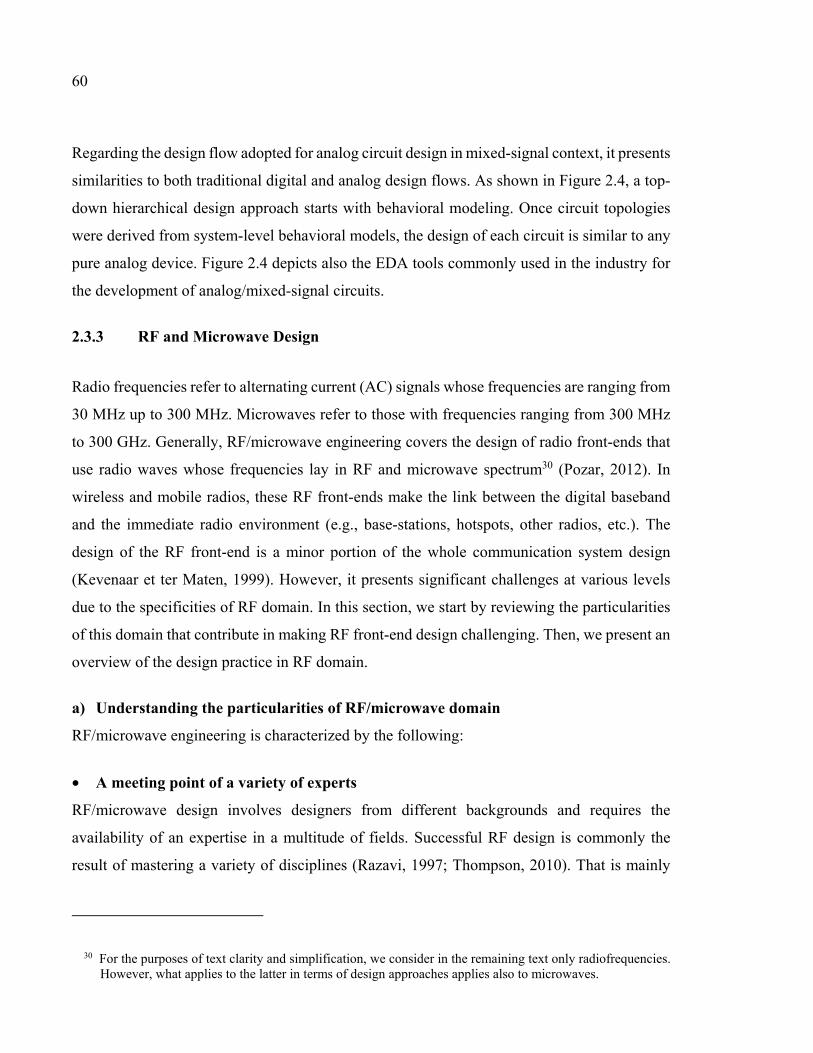
60
Regarding the design flow adopted for analog circuit design in mixed-signal context, it presents
similarities to both traditional digital and analog design flows. As shown in Figure 2.4, a top-
down hierarchical design approach starts with behavioral modeling. Once circuit topologies
were derived from system-level behavioral models, the design of each circuit is similar to any
pure analog device. Figure 2.4 depicts also the EDA tools commonly used in the industry for
the development of analog/mixed-signal circuits.
2.3.3 RF and Microwave Design
Radio frequencies refer to alternating current (AC) signals whose frequencies are ranging from
30 MHz up to 300 MHz. Microwaves refer to those with frequencies ranging from 300 MHz
to 300 GHz. Generally, RF/microwave engineering covers the design of radio front-ends that
use radio waves whose frequencies lay in RF and microwave spectrum30 (Pozar, 2012). In
wireless and mobile radios, these RF front-ends make the link between the digital baseband
and the immediate radio environment (e.g., base-stations, hotspots, other radios, etc.). The
design of the RF front-end is a minor portion of the whole communication system design
(Kevenaar et ter Maten, 1999). However, it presents significant challenges at various levels
due to the specificities of RF domain. In this section, we start by reviewing the particularities
of this domain that contribute in making RF front-end design challenging. Then, we present an
overview of the design practice in RF domain.
a) Understanding the particularities of RF/microwave domain
RF/microwave engineering is characterized by the following:
• A meeting point of a variety of experts
RF/microwave design involves designers from different backgrounds and requires the
availability of an expertise in a multitude of fields. Successful RF design is commonly the
result of mastering a variety of disciplines (Razavi, 1997; Thompson, 2010). That is mainly
30 For the purposes of text clarity and simplification, we consider in the remaining text only radiofrequencies. However, what applies to the latter in terms of design approaches applies also to microwaves.
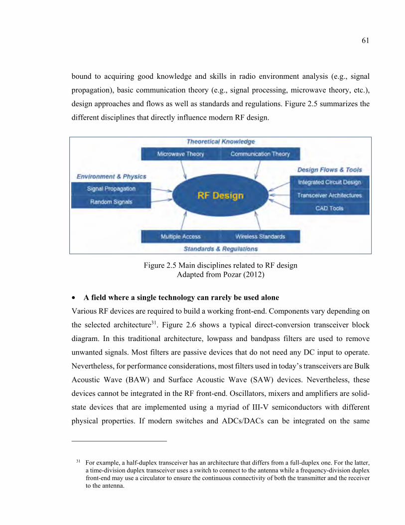
61
bound to acquiring good knowledge and skills in radio environment analysis (e.g., signal
propagation), basic communication theory (e.g., signal processing, microwave theory, etc.),
design approaches and flows as well as standards and regulations. Figure 2.5 summarizes the
different disciplines that directly influence modern RF design.
Figure 2.5 Main disciplines related to RF design Adapted from Pozar (2012)
• A field where a single technology can rarely be used alone
Various RF devices are required to build a working front-end. Components vary depending on
the selected architecture31. Figure 2.6 shows a typical direct-conversion transceiver block
diagram. In this traditional architecture, lowpass and bandpass filters are used to remove
unwanted signals. Most filters are passive devices that do not need any DC input to operate.
Nevertheless, for performance considerations, most filters used in today’s transceivers are Bulk
Acoustic Wave (BAW) and Surface Acoustic Wave (SAW) devices. Nevertheless, these
devices cannot be integrated in the RF front-end. Oscillators, mixers and amplifiers are solid-
state devices that are implemented using a myriad of III-V semiconductors with different
physical properties. If modern switches and ADCs/DACs can be integrated on the same
31 For example, a half-duplex transceiver has an architecture that differs from a full-duplex one. For the latter, a time-division duplex transceiver uses a switch to connect to the antenna while a frequency-division duplex front-end may use a circulator to ensure the continuous connectivity of both the transmitter and the receiver to the antenna.
62
substrate on which the baseband circuitry is implemented, ferrite-based components (e.g.,
isolators, circulators) cannot. In most wireless and mobile devices, antennas are passive but
cumbersome structures which are hardly integrated in the RF front-end due to their physical
dimensions (Robertson et Lucyszyn, 2009; Sorrentino et Bianchi, 2010). This mix of
technologies is challenging for a number of reasons (e.g., integration, heat dissipation, etc.)
especially when a small form-factor is required.
• A domain highly sensitive to impairments and nonlinearities
By opposition to digital circuitry, RF devices are very sensitive to noise, signal distortion and
inherent radio impairments. Each RF component adds an amount of noise to the signal. The
cumulative value of added noise depends on the way the RF components are mounted. It
reduces the transceiver’s signal-to-noise ratio, which influences negatively the data rate. Signal
distortion occurs due to the imperfections and the nonlinearity of RF devices. For example, a
power amplifier crops a signal when its input power lies above its compression point (see
Figure 2.7.a). In the presence of multiple tones, nonlinearity of active devices (e.g., mixer,
amplifier) produces intermodulation products. These harmonics are unwanted signals that
appear in multiple sum and difference frequencies of the original tones (see Figure 2.7.b). In
transmission, these unwanted signals pollute the spectrum and interferes with other radios. In
reception, some of these harmonics may interfere with desired signals. Poor isolation in
transceivers as well as adjacent channel signals are common sources of strong signals that mix
with local signals and cause severe inband interferers. Reducing the impact of noise and
mitigating the effect of inherent radio impairments is a major challenge in RF design.
• A discipline of compromises and trade-offs
RF design is governed by a set of antagonistic system-level parameters. Figure 2.8 shows the
“RF Design Hexagon”, an assembly of six mutually-dependent variables, having a significant
impact on RF design (i.e., frequency, power, DC supply voltage, gain, noise and linearity)
(Razavi, 1998). The change of one of them affects the others. For example, increasing input
power requires more supply voltage. Depending on frequency, it changes linearity. If linearity
changes, the corresponding gain changes too. In addition, more power means increasing noise.
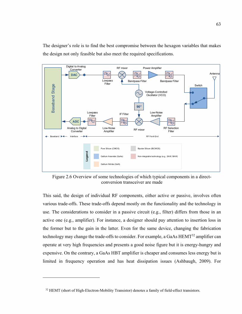
63
The designer’s role is to find the best compromise between the hexagon variables that makes
the design not only feasible but also meet the required specifications.
DAC
Bas
eba
nd S
tage
Lowpass Filter
Voltage-Controlled Oscillator (VCO)
Digital to Analog Converter
RF mixer Power Amplifier
Bandpass Filter
Switch
Antenna
90°
RF Selection Filter
Low-Noise Amplifier
RF mixer
IF Filter
Low-Noise Amplifier
Lowpass Filter
ADC
Analog to Digital Converter
Bandpass Filter
RF Front-End
Pure Silicon (CMOS)
Gallium Arsenide (GaAs)
Gallium Nitride (GaN)
InterfaceBaseband
Bipolar Silicon (BiCMOS)
Non-integrable technology (e.g., SAW, BAW)
Figure 2.6 Overview of some technologies of which typical components in a direct-conversion transceiver are made
This said, the design of individual RF components, either active or passive, involves often
various trade-offs. These trade-offs depend mostly on the functionality and the technology in
use. The considerations to consider in a passive circuit (e.g., filter) differs from those in an
active one (e.g., amplifier). For instance, a designer should pay attention to insertion loss in
the former but to the gain in the latter. Even for the same device, changing the fabrication
technology may change the trade-offs to consider. For example, a GaAs HEMT32 amplifier can
operate at very high frequencies and presents a good noise figure but it is energy-hungry and
expensive. On the contrary, a GaAs HBT amplifier is cheaper and consumes less energy but is
limited in frequency operation and has heat dissipation issues (Ashbaugh, 2009). For
32 HEMT (short of High-Electron-Mobility Transistor) denotes a family of field-effect transistors.
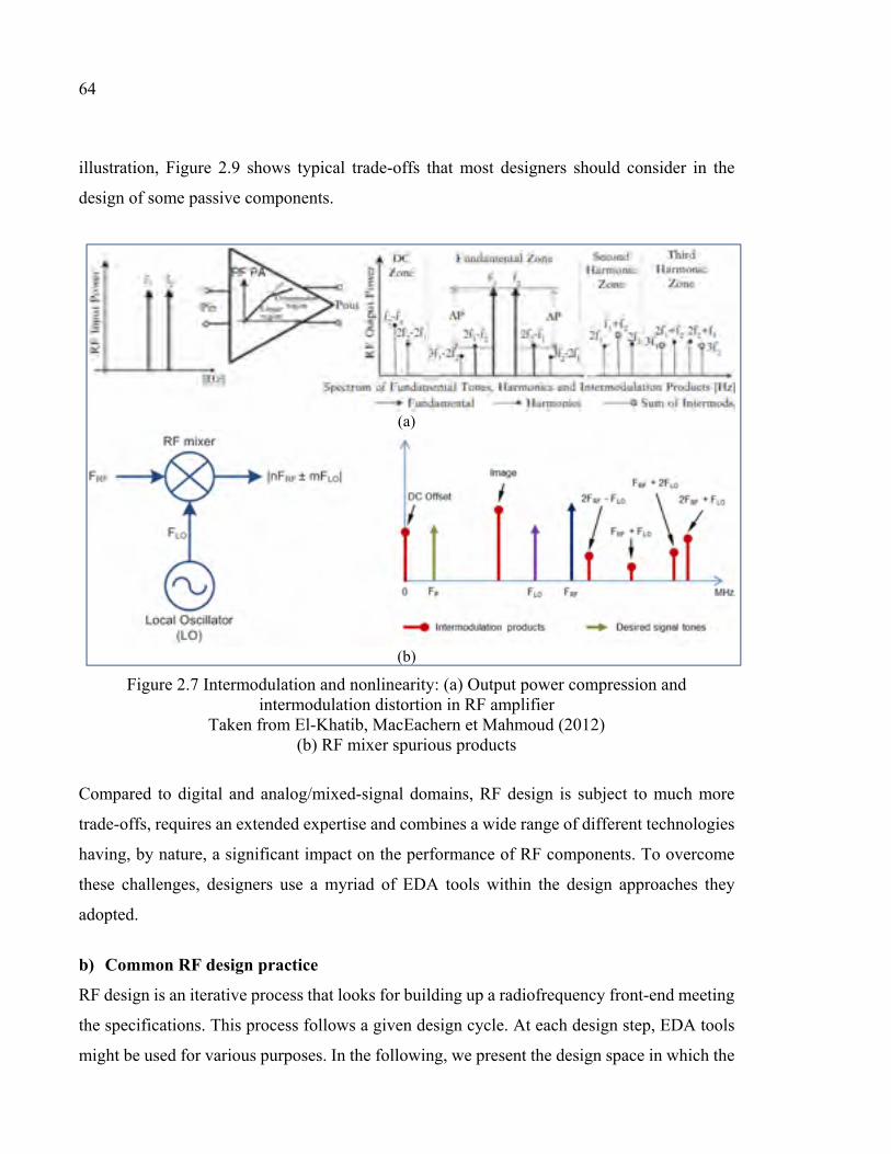
64
illustration, Figure 2.9 shows typical trade-offs that most designers should consider in the
design of some passive components.
(a)
(b)
Figure 2.7 Intermodulation and nonlinearity: (a) Output power compression and intermodulation distortion in RF amplifier
Taken from El-Khatib, MacEachern et Mahmoud (2012) (b) RF mixer spurious products
Compared to digital and analog/mixed-signal domains, RF design is subject to much more
trade-offs, requires an extended expertise and combines a wide range of different technologies
having, by nature, a significant impact on the performance of RF components. To overcome
these challenges, designers use a myriad of EDA tools within the design approaches they
adopted.
b) Common RF design practice
RF design is an iterative process that looks for building up a radiofrequency front-end meeting
the specifications. This process follows a given design cycle. At each design step, EDA tools
might be used for various purposes. In the following, we present the design space in which the
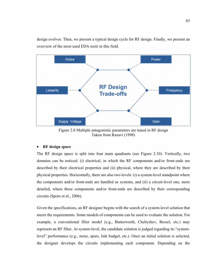
65
design evolves. Then, we present a typical design cycle for RF design. Finally, we present an
overview of the most used EDA tools in this field.
Figure 2.8 Multiple antagonistic parameters are tuned in RF design Taken from Razavi (1998)
• RF design space
The RF design space is split into four main quadrants (see Figure 2.10). Vertically, two
domains can be noticed: (i) electrical, in which the RF components and/or front-ends are
described by their electrical properties and (ii) physical, where they are described by their
physical properties. Horizontally, there are also two levels: (i) a system-level standpoint where
the components and/or front-ends are handled as systems, and (ii) a circuit-level one, more
detailed, where these components and/or front-ends are described by their corresponding
circuits (Spoto et al., 2006).
Given the specifications, an RF designer begins with the search of a system-level solution that
meets the requirements. Some models of components can be used to evaluate the solution. For
example, a conventional filter model (e.g., Butterworth, Chebyshev, Bessel, etc.) may
represent an RF filter. At system-level, the candidate solution is judged regarding its “system-
level” performance (e.g., noise, spurs, link budget, etc.). Once an initial solution is selected,
the designer develops the circuits implementing each component. Depending on the
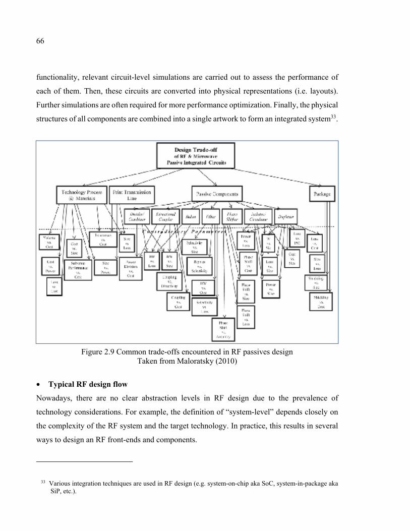
66
functionality, relevant circuit-level simulations are carried out to assess the performance of
each of them. Then, these circuits are converted into physical representations (i.e. layouts).
Further simulations are often required for more performance optimization. Finally, the physical
structures of all components are combined into a single artwork to form an integrated system33.
Figure 2.9 Common trade-offs encountered in RF passives design Taken from Maloratsky (2010)
• Typical RF design flow
Nowadays, there are no clear abstraction levels in RF design due to the prevalence of
technology considerations. For example, the definition of “system-level” depends closely on
the complexity of the RF system and the target technology. In practice, this results in several
ways to design an RF front-ends and components.
33 Various integration techniques are used in RF design (e.g. system-on-chip aka SoC, system-in-package aka SiP, etc.).
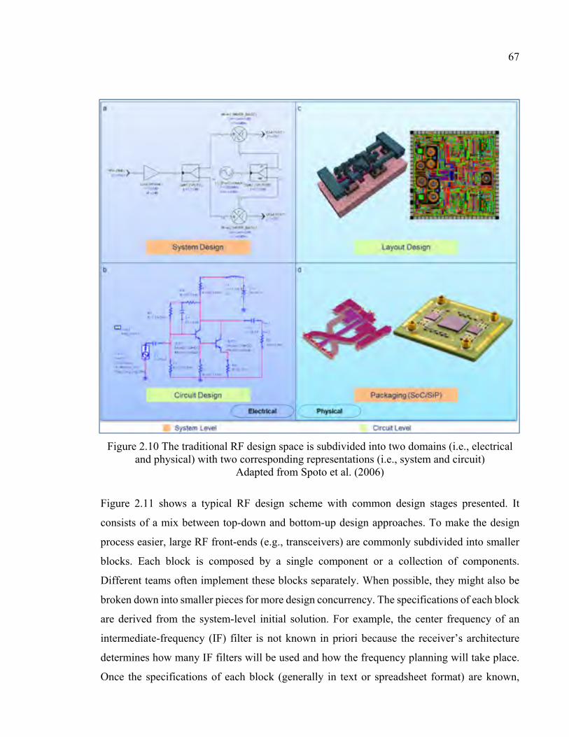
67
Figure 2.10 The traditional RF design space is subdivided into two domains (i.e., electrical and physical) with two corresponding representations (i.e., system and circuit)
Adapted from Spoto et al. (2006)
Figure 2.11 shows a typical RF design scheme with common design stages presented. It
consists of a mix between top-down and bottom-up design approaches. To make the design
process easier, large RF front-ends (e.g., transceivers) are commonly subdivided into smaller
blocks. Each block is composed by a single component or a collection of components.
Different teams often implement these blocks separately. When possible, they might also be
broken down into smaller pieces for more design concurrency. The specifications of each block
are derived from the system-level initial solution. For example, the center frequency of an
intermediate-frequency (IF) filter is not known in priori because the receiver’s architecture
determines how many IF filters will be used and how the frequency planning will take place.
Once the specifications of each block (generally in text or spreadsheet format) are known,
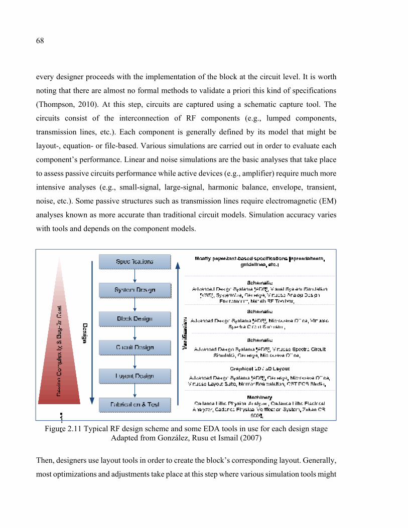
68
every designer proceeds with the implementation of the block at the circuit level. It is worth
noting that there are almost no formal methods to validate a priori this kind of specifications
(Thompson, 2010). At this step, circuits are captured using a schematic capture tool. The
circuits consist of the interconnection of RF components (e.g., lumped components,
transmission lines, etc.). Each component is generally defined by its model that might be
layout-, equation- or file-based. Various simulations are carried out in order to evaluate each
component’s performance. Linear and noise simulations are the basic analyses that take place
to assess passive circuits performance while active devices (e.g., amplifier) require much more
intensive analyses (e.g., small-signal, large-signal, harmonic balance, envelope, transient,
noise, etc.). Some passive structures such as transmission lines require electromagnetic (EM)
analyses known as more accurate than traditional circuit models. Simulation accuracy varies
with tools and depends on the component models.
Figure 2.11 Typical RF design scheme and some EDA tools in use for each design stage Adapted from González, Rusu et Ismail (2007)
Then, designers use layout tools in order to create the block’s corresponding layout. Generally,
most optimizations and adjustments take place at this step where various simulation tools might
69
be used to verify the final design performance (e.g., signal reflection, gain, noise, shielding
properties, radiation, etc.).
The next step consists of prototype manufacturing and testing. Sometimes final integration
takes place before manufacturing. This happens commonly with passive structures where all
components are combined and manufactured together. In other cases, individual components
might be entirely developed and tested separately before their integration into the final solution
(e.g., SAW filters). Simulated and measured performances rarely match due the inaccuracies
in device modeling and simulation tools as well as the variability of fabrication processes. For
this reason, most designers consider a margin to compensate any eventual degradation
particularly in critical-performance applications. Furthermore, the verification process is
iterative. Once an error is detected, the previous step is revisited. These re-spins are time-
consuming. The cost of error correction may be prohibitively expensive particularly at
advanced design stages such as final integration (Thompson, 2010).
• EDA tools for RF design
RF EDA tools have seen remarkable progress during the last two decades. As discussed in
(Cheng et al., 2010), existent tools provide designers with valuable features such as:
− Optimization algorithms and tuning options,
− Statistical design options: yield, sensitivity, etc.,
− Support of industry standard file formats (e.g., Touchstone, P2D, GDSII, Gerber, etc.),
− 2D and 3D EM analysis technology,
− Connectivity with test and measurement platforms (e.g., vector network analyzers,
waveform generators, etc.),
− Component vendor libraries,
− Wireless standards test benches and design libraries,
− Various design guides and synthesis tools (e.g., filters, oscillators),
− Support of file- and equation-based models,
− Tools for budget, spurs and intermodulation analysis.
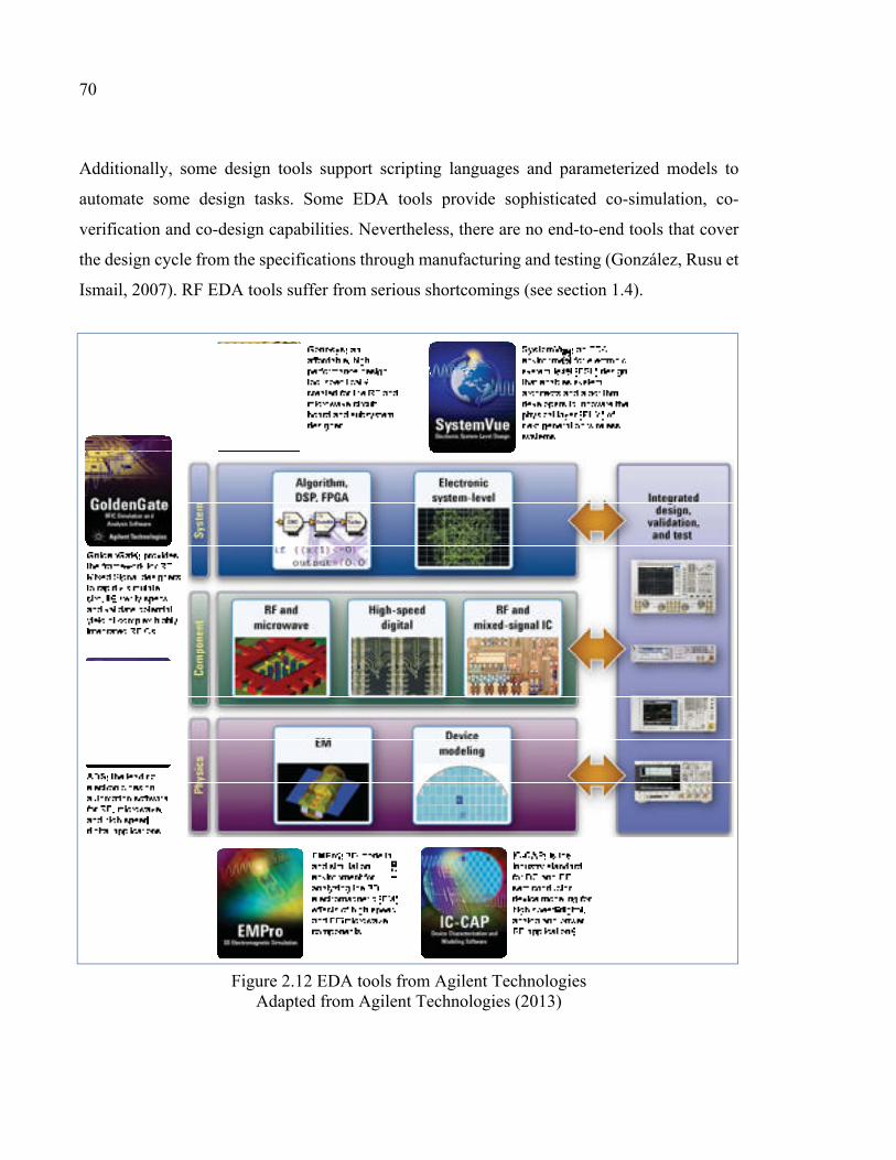
70
Additionally, some design tools support scripting languages and parameterized models to
automate some design tasks. Some EDA tools provide sophisticated co-simulation, co-
verification and co-design capabilities. Nevertheless, there are no end-to-end tools that cover
the design cycle from the specifications through manufacturing and testing (González, Rusu et
Ismail, 2007). RF EDA tools suffer from serious shortcomings (see section 1.4).
Figure 2.12 EDA tools from Agilent Technologies Adapted from Agilent Technologies (2013)
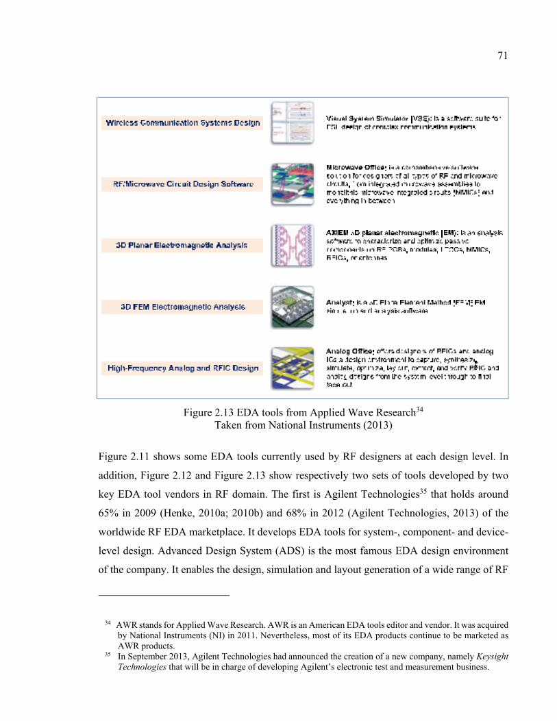
71
Figure 2.13 EDA tools from Applied Wave Research34 Taken from National Instruments (2013)
Figure 2.11 shows some EDA tools currently used by RF designers at each design level. In
addition, Figure 2.12 and Figure 2.13 show respectively two sets of tools developed by two
key EDA tool vendors in RF domain. The first is Agilent Technologies35 that holds around
65% in 2009 (Henke, 2010a; 2010b) and 68% in 2012 (Agilent Technologies, 2013) of the
worldwide RF EDA marketplace. It develops EDA tools for system-, component- and device-
level design. Advanced Design System (ADS) is the most famous EDA design environment
of the company. It enables the design, simulation and layout generation of a wide range of RF
34 AWR stands for Applied Wave Research. AWR is an American EDA tools editor and vendor. It was acquired by National Instruments (NI) in 2011. Nevertheless, most of its EDA products continue to be marketed as AWR products.
35 In September 2013, Agilent Technologies had announced the creation of a new company, namely Keysight Technologies that will be in charge of developing Agilent’s electronic test and measurement business.
72
devices and systems. It includes various types of linear and nonlinear, time- and frequency-
domain simulators (Agilent Technologies, 2013). The second is Applied Wave Research,
which is one of the major competitors of Agilent. The company develops Microwave Office,
an integrated RF and microwave design software, a competitor product of ADS. Both
companies also develop system-level cross-domain design tools (i.e., SystemVue of Agilent
and Visual System Simulator of AWR). In addition, they developed various EM analysis and
simulation products (e.g., EMPro of Agilent, AXIEM 3D and Analyst of AWR) (Agilent
Technologies, 2013; National Instruments, 2013).
2.4 Comparative Study of Design Practice through Domains
As depicted in the previous section, there are various differences between digital,
analog/mixed-signal and RF/microwave domains. There are also some disparities regarding
the design practice in each of these domains. In this section, we attempt to compare the design
practices in terms of design approaches and with the subsequent technology impact.
• Technology impact through design domains
Digital chips contain millions of transistors. Analog ones are composed of few hundreds (up
to few thousands) of them while RF circuits are composed of only few (tens of) transistors
(Grant, 2012). Analog circuits use larger area and are less dense than digital ones (Lavagno,
Martin et Scheffer, 2006). This is also true for RF circuits. Hierarchical design approach and
mature EDA tools allow digital designers to handle complex chips. However, EDA tools are
not fast enough to deal with large analog and RF circuits (Blyler, 2006). Digital designers look
for more performance with the smallest possible area and power consumption. On the contrary,
their analog counterparts focus more on accuracy while the RF designers are struggling only
to get things working properly (Grant, 2012). If digital chips are often implemented using a
single technology (i.e., silicon-based), analog (and RF) circuits can be implemented using a
variety of fabrication technologies (e.g., Gallium Arsenide aka GaAs, Gallium Nitride aka
GaN, etc.). In digital design, a standard design process exists. However, there is a need for
integrated tools and design processes that suits better for this mix of technologies in both
73
analog and RF domains (Viklund, 2005). The required multi-technology support includes the
simulation of different technologies at system-level (Park, Hartung et Dudek, 2007).
In addition, moving from a technology process to another in digital design is relatively easy
while it is difficult and not cost-effective for both analog and RF domains. One of the reasons
behind this situation is the maturity of digital design tools while those used in analog and RF
domain are still in their infancy (Hansen, 2003). Furthermore, CMOS scaling36 brings higher
integration and less power consumption in digital domain while it causes significant reduction
in dynamic range37 for both analog and RF circuits (Hansen, 2003). Thus, it is important to
provide RF designers with tools to address these issues (Gielen, 2007). Table 2.2 summarizes
some characteristics of the three domains from a technological standpoint.
• Abstraction, Modeling and Device Characterization
In digital design, there are five abstraction levels that were adopted (i.e., device, circuit, gate,
module and system) (Rabaey, Chandrakasan et Nikolic, 2002). It is also common to consider
three abstraction levels (i.e. device, circuit/macro, system) for silicon-based analog/mixed-
signal designs (Allen et Holberg, 2002). Nevertheless, there are no clear abstraction levels in
RF domain. This absence of abstraction contributes to at least two issues: (i) there is no formal
way to model components and systems, and (ii) it is not possible to automate the transition
between the different abstraction levels.
In fact, if device models are relatively easy to create, use and export in digital design and
partially available for silicon-based analog/mixed-signal processes, it is not the same in RF
domain. The absence of formal modeling in this domain causes, for example:
− Serious limitations in system-level modeling which hinders early design verification
(Dunham et al., 2003),
36 CMOS scaling allows higher speed via the increase of transistor current and smaller area via the increase of the chip’s density Hu, Chenming. 1993. « Future CMOS scaling and reliability ». Proceedings of the IEEE, vol. 81, no 5, p. 682-689.
37 The reduction of supply voltage by 20% decreases the dynamic range by almost 1.6 dB. Hansen, K. 2003. « Wireless RF design challenges ». 2003 Ieee Radio Frequency Integrated Circuits (Rfic) Symposium, Digest of Papers, p. 3-7.
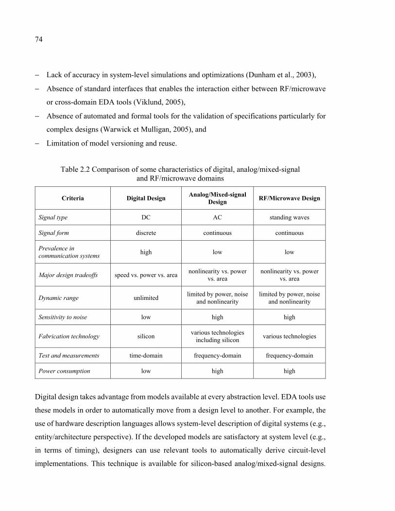
74
− Lack of accuracy in system-level simulations and optimizations (Dunham et al., 2003),
− Absence of standard interfaces that enables the interaction either between RF/microwave
or cross-domain EDA tools (Viklund, 2005),
− Absence of automated and formal tools for the validation of specifications particularly for
complex designs (Warwick et Mulligan, 2005), and
− Limitation of model versioning and reuse.
Table 2.2 Comparison of some characteristics of digital, analog/mixed-signal and RF/microwave domains
Criteria Digital Design Analog/Mixed-signal
Design RF/Microwave Design
Signal type DC AC standing waves
Signal form discrete continuous continuous
Prevalence in communication systems
high low low
Major design tradeoffs speed vs. power vs. area nonlinearity vs. power
vs. area nonlinearity vs. power
vs. area
Dynamic range unlimited limited by power, noise
and nonlinearity limited by power, noise
and nonlinearity
Sensitivity to noise low high high
Fabrication technology silicon various technologies
including silicon various technologies
Test and measurements time-domain frequency-domain frequency-domain
Power consumption low high high
Digital design takes advantage from models available at every abstraction level. EDA tools use
these models in order to automatically move from a design level to another. For example, the
use of hardware description languages allows system-level description of digital systems (e.g.,
entity/architecture perspective). If the developed models are satisfactory at system level (e.g.,
in terms of timing), designers can use relevant tools to automatically derive circuit-level
implementations. This technique is available for silicon-based analog/mixed-signal designs.
75
Analog designers use mostly either dedicated hardware description languages such as VHDL-
AMS/Verilog-A or conventional programming languages (e.g., SystemC). However, this
technique cannot be used in RF design, which limits automation capability in this domain.
This said, technology insertion is valuable for radio design. Digital designers use standard
libraries for the simulation of digital circuits. This also happens with analog/mixed-signal and
RF designs. However, these libraries are less accurate and more complex than their digital
counterparts (Dunham et al., 2003). Technology libraries used for the latter should provide
accurate device models (McMahon, 2009). In addition, these libraries should provide complete
analog/RF device characterization including its response to the various effects and parasitics
(Dunham et al., 2003). All this should take place in a context of technology mix.
• Readiness for Mixed-Signal Co-Design
Most Recent radio chips are mixed-signal. (Rutenbar, 2006) estimates that 3 out of 4 digital
chips include analog content. (Allen et Holberg, 2002) claims that digital circuitry covers 80%
of a typical mixed-signal chip area while the remaining 20% are dedicated for analog circuitry.
Furthermore, (Akretch, 2012) argues that mixing RF circuits with their digital and analog
counterparts causes signal integrity38 problems. First, digital circuits are tested in time-domain
while analog and RF ones are tested in frequency domain. There is a lack in tools for the
correlation between digital and analog/RF signals (Akretch, 2012). Then, a part of the problem
is the absence of relevant interfaces across domains (Dunham et al., 2003). This leads to
various shortcomings not only in RF/microwave but also in digital and analog domains. In
digital design, RF circuits are treated as black boxes where underlying circuits are not detailed
and their response is often represented by inaccurate models. Moreover, both digital and analog
EDA tools lack the ability of simulating RF circuits. On the one hand, there is a lack of tool
integration in these domains (Dunham et al., 2003). On the other hand, specialized RF tools
are not the only solution for better mixed-signal design (Viklund, 2005). A schematic-driven
38 Digital circuits are noise-immune while they generate an abundance of noise. Analog and RF circuits are very sensitive to that noise. Blyler, John. 2006. « Analog-RF IP Integration Challenges SoC Designers ». Chip Design Magazine. < http://chipdesignmag.com/display.php?articleId=435 >. Consulté le 26 February 2014.
76
flow is also not always optimal neither purely layout-driven design is feasible due to RF
integration issues (Viklund, 2005). To increase the capability for better mixed-signal design
through the different domains, standard interfaces should be developed to enhance mutual
understanding between the various design disciplines. An integrated design environment for
functional, performance and closed-loop verification across domains and across multiple
technologies empowered by comprehensive simulation solutions at different abstraction levels
is required (Park, Hartung et Dudek, 2007).
• Productivity
The RF front-end is the smallest part in wireless and mobile radios. However, it mobilizes the
most of design time and effort. One of the reasons behind this situation is the multiple re-spins
and iterations for a first success in both analog/mixed-signal and RF designs (Hansen, 2003;
Maloratsky, 2010; Zhang et al., 2004). In fact, complex digital chips can be designed correctly
on the first attempt and in only few months while a complex analog chip requires 3 to 4
iterations and up to 18 months (Kundert et al., 2000). More recently, it is assumed to spend 2
to 3 passes for a defect-free analog chip against only one pass for a digital one (Allen et
Holberg, 2002). Designers spend 3 to 7 times more effort per transistor in analog than in digital
design (Kundert et al., 2000). RF designs require also multiple passes to complete a circuit
(Hansen, 2003). Then, it becomes obvious that productivity in digital design is greater than in
analog/mixed-signal and RF domain. At this regard, (Kundert et al., 2000) argues that
automation and design reuse are among the basic factors to increase design productivity.
In digital domain, a significant portion of design is automated due to the availability of highly
specialized set of tools. However, RF design in a traditional design environment is mostly
manual (Viklund, 2005). By nature, RF design is highly sensitive to a variety of effects (e.g.,
parasitics, substrate, packaging, etc.). There are no tools to satisfy all these analyses and at a
decent speed (Hansen, 2003). Current tools do what are they best at. Additionally, some errors
are caused by the misinterpretation of specifications (frequently due to the use of ambiguous
language) (Park, Hartung et Dudek, 2007). The effect of this ambiguity might increase in
mixed-signal design because design collaboration is mostly manual or even non-existent at all
(Park, Hartung et Dudek, 2007). For all these reasons, there is a growing need in enhancing
77
automation especially in analog/mixed-signal and RF design (Viklund, 2005) where providing
designers with fast and highly-specialized EDA tools is also essential (Blyler, 2006;
McMahon, 2009).
Digital designers rely on modeling to reuse designs. IP blocks enable them to produce several
versions of their designs and use them for the development of other systems. In analog/mixed-
signal domain, IP blocks can also be used (e.g., low-noise amplifiers) (Dunham et al., 2003).
However, versioning and reuse is very limited in RF designs.
In summary, digital design is relatively the most developed discipline in radio design. This is
due to the well-developed design practice that is particularly empowered by mature tools. The
design practice in analog/mixed-signal design evolved during the last years especially for
silicon-based technologies where some digital-like concepts were applied. In RF domain, tools
have significantly evolved but the design practice has still more room to evolve. There is a
growing need for more efforts to be deployed in order to enhance productivity, bring more
automation and open this expert-domain for non-expert designers. To conclude, Table 2.3
presents a comparative of design practice in digital, analog/mixed-signal and RF/microwave
domains.
2.5 Conclusion
The design practice has significantly evolved in radio design. In this second chapter, we aimed
at developing a better understanding of this practice in the different domains pertaining to radio
design. Therefore, we started with presenting an overview of design common design
approaches used in radio design as well as the future requirements of EDA tools to be used
within these approaches. Then, we discussed with some detail the modern design practice in
digital, analog/mixed-signal and RF and microwave domains. We concluded the chapter with
a comparative study of the design practice within these three domains.
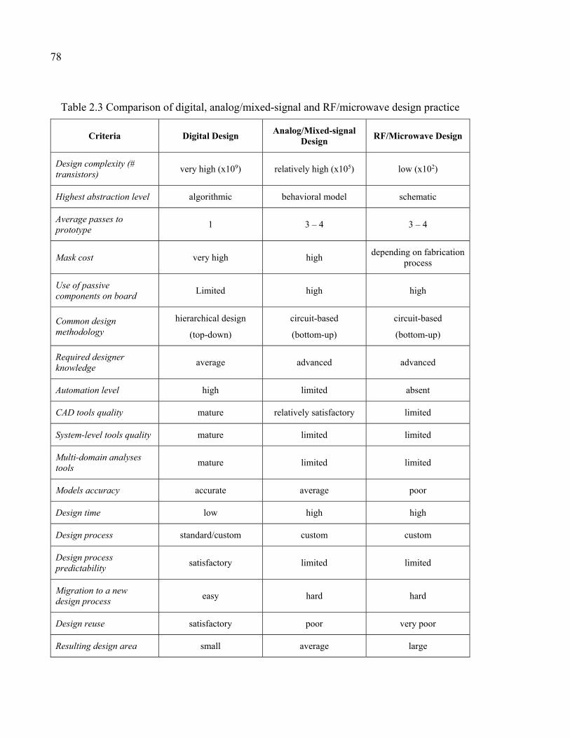
78
Table 2.3 Comparison of digital, analog/mixed-signal and RF/microwave design practice
Criteria Digital Design Analog/Mixed-signal
Design RF/Microwave Design
Design complexity (# transistors)
very high (x109) relatively high (x105) low (x102)
Highest abstraction level algorithmic behavioral model schematic
Average passes to prototype
1 3 – 4 3 – 4
Mask cost very high high depending on fabrication
process
Use of passive components on board
Limited high high
Common design methodology
hierarchical design
(top-down)
circuit-based
(bottom-up)
circuit-based
(bottom-up)
Required designer knowledge
average advanced advanced
Automation level high limited absent
CAD tools quality mature relatively satisfactory limited
System-level tools quality mature limited limited
Multi-domain analyses tools
mature limited limited
Models accuracy accurate average poor
Design time low high high
Design process standard/custom custom custom
Design process predictability
satisfactory limited limited
Migration to a new design process
easy hard hard
Design reuse satisfactory poor very poor
Resulting design area small average large
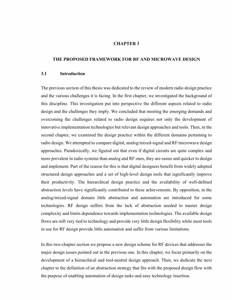
CHAPTER 3
THE PROPOSED FRAMEWORK FOR RF AND MICROWAVE DESIGN
3.1 Introduction
The previous section of this thesis was dedicated to the review of modern radio design practice
and the various challenges it is facing. In the first chapter, we investigated the background of
this discipline. This investigation put into perspective the different aspects related to radio
design and the challenges they imply. We concluded that meeting the emerging demands and
overcoming the challenges related to radio design requires not only the development of
innovative implementation technologies but relevant design approaches and tools. Then, in the
second chapter, we examined the design practice within the different domains pertaining to
radio design. We attempted to compare digital, analog/mixed-signal and RF/microwave design
approaches. Paradoxically, we figured out that even if digital circuits are quite complex and
more prevalent in radio systems than analog and RF ones, they are easier and quicker to design
and implement. Part of the reason for this is that digital designers benefit from widely adopted
structured design approaches and a set of high-level design tools that significantly improve
their productivity. The hierarchical design practice and the availability of well-defined
abstraction levels have significantly contributed to these achievements. By opposition, in the
analog/mixed-signal domain little abstraction and automation are introduced for some
technologies. RF design suffers from the lack of abstraction needed to master design
complexity and limits dependence towards implementation technologies. The available design
flows are still very tied to technology and provide very little design flexibility while most tools
in use for RF design provide little automation and suffer from various limitations.
In this two-chapter section we propose a new design scheme for RF devices that addresses the
major design issues pointed out in the previous one. In this chapter, we focus primarily on the
development of a hierarchical and tool-neutral design approach. Then, we dedicate the next
chapter to the definition of an abstraction strategy that fits with the proposed design flow with
the purpose of enabling automation of design tasks and easy technology insertion.

80
3.2 Scope and Objectives
In section 1.4, we enumerated some of current challenges and issues related to both design
flows and tools used in modern RF domain. These challenges can be roughly classified into
five major categories:
1. Productivity: it relates to techniques and mechanisms used in order to minimize the
required effort, time and money to get a successful design (e.g., design concurrency,
automation, etc.);
2. Design collaboration: it is interested in methods used to improve the communication
between different designers (and also the interaction between design tools) and enhance
collaborative work within the design cycle (e.g., tools interaction, design data exchange,
team collaboration, etc.);
3. Design flexibility: it relates to techniques enabling the reuse of the same design in multiple
contexts (e.g., versioning and design reuse);
4. Design accuracy: it is interested in the performance of design tools in terms of precision
and correctness (e.g., simulation accuracy, tool specialization, modeling accuracy, etc.);
5. Technology support: it focuses on the mechanisms enabling the management of technology
details (e.g., multi-technology support).
The development of future RF front-ends requires these issues to be addressed. We estimate
that an effective solution can be an end-to-end integrated design flow that allows hierarchical
and collaborative design. In addition, such design flow should define coherent mechanisms
enabling handy technology insertion and allowing non-expert designers to easily implement
their front-ends. It should also include automation and design concurrency processes for
productivity enhancement.
Accordingly, our objective in the following is the development of a new design framework,
which is built around a refurbished design flow for the development of RF components. We
are particularly interested in the development of the relevant mechanisms and processes that
empower the intended design framework with the properties summarized in Table 3.1.
81
Table 3.1 Summary of the properties that the intended RF design framework is expected to support
Code Property Description
P1 Automation The ability of (semi-)automatically conducting one or many design tasks within the design flow.
P2 Data exchange
The ability of exchanging design data (e.g., models, simulation data, technology information, etc.) in a fully comprehensive manner between the different design steps (with respect to both designers and tools).
P3 Design collaboration The ability of easing communication, knowledge flow and mutual understanding between teammates in the perspective of endorsing the overall team productivity.
P4 Design concurrency The capacity of enabling concurrent design tasks where different jobs can be carried out in parallel.
P5 Design consistency The ability of ensuring the coherency and the correctness of the design.
P6 Design reuse The capability of using the same design, either in part or in whole, in a new design with minor or no changes.
P7 Technology insertion The ability of using new technology data and models in design with no or very limited upgrades of the tools in use.
P8 Tools interaction The capacity of tools to interact, automatically or with minor human assistance, in order to cooperatively carry out intended design tasks.
3.3 Proposal of a New Framework to Bridge Existing Design Gaps
Unlike the typical RF design scheme where handling technology often starts at the early design
steps (see Figure 2.11), we propose in this section a hierarchical design flow that virtually
pushes physical details to the latest design stages. For better illustration, the design flow is
presented hereafter incrementally in order to thoroughly describe the different mechanisms and
artefacts that are meant to support properties enumerated in Table 3.1.
82
3.3.1 A Five-Step Design Scheme
The proposed design flow consists of five main design steps (see Figure 3.1). The design starts
with the component’s specifications. These specifications are then analyzed and validated in
the “Analysis” step. In this phase, the designer carries out a design space exploration seeking
for a design solution that meets the given specifications. If an initial solution is found, it is
investigated, optimized and implemented in the “Synthesis” step considering the relevant
technology input. “Synthesis” is meant to be automated as much as possible. It results in a
ready-to-manufacture design that is fabricated in the next step, namely “Manufacturing”. Once
fabricated, the prototype is submitted for final verification in the last design step, namely “Tests
and Measurements”.
This said, which mechanisms and artefacts might be adopted in order to enable higher
automation and design collaboration and alleviate the various previously mentioned
challenges?
3.3.2 Functional Description
In traditional RF design, specifications are text-based and cannot be validated using specialized
tools. This explains in part why designers start by tweaking the physical details of their circuits
looking for a suitable design solution. This mostly manual task may take a valuable time with
no satisfactory results because the specifications could be neither coherent nor realistic. In this
regard, we propose a new concept namely “Functional Description”. The idea behind this is
first, to uncouple the component’s function from its underlying physical structure. Then, our
ultimate goal is to establish an “executable specifications” process that helps to validate
specifications at the early phases of design and figure out any inconsistencies and errors. It is
worth noting that the paradigm of executable specifications was introduced in software
engineering domain (Cardinal, 2013). Particularly, it was used in agile software development
to enable test-driven development where the implementation is constantly checked against the
evolving requirements. This concept has been expanding to other engineering fields. For
instance, it was used in digital design not only to capture design requirements and constraints
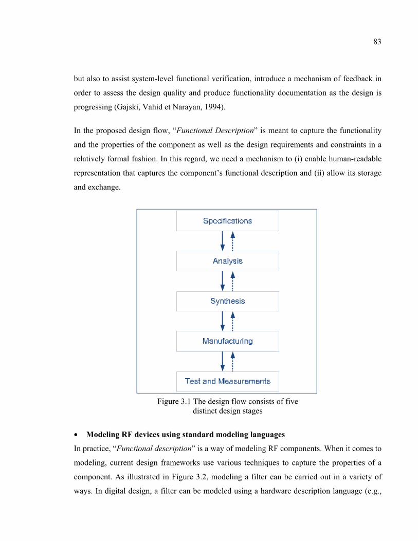
83
but also to assist system-level functional verification, introduce a mechanism of feedback in
order to assess the design quality and produce functionality documentation as the design is
progressing (Gajski, Vahid et Narayan, 1994).
In the proposed design flow, “Functional Description” is meant to capture the functionality
and the properties of the component as well as the design requirements and constraints in a
relatively formal fashion. In this regard, we need a mechanism to (i) enable human-readable
representation that captures the component’s functional description and (ii) allow its storage
and exchange.
Figure 3.1 The design flow consists of five distinct design stages
• Modeling RF devices using standard modeling languages
In practice, “Functional description” is a way of modeling RF components. When it comes to
modeling, current design frameworks use various techniques to capture the properties of a
component. As illustrated in Figure 3.2, modeling a filter can be carried out in a variety of
ways. In digital design, a filter can be modeled using a hardware description language (e.g.,
84
VHDL). Either traditional programming languages (e.g., C++) or custom ones (e.g., SystemC)
can also be used to model an analog filter. RF tools use graphical blocks to capture the
parameters of a filter at system level (e.g., ADS, SystemVue). All these representations are
good to capture the properties of the intended filter. Nevertheless, they may be limited in
flexibility. For example, system-level blocks used within ADS and SystemVue are predefined.
They cannot be directly altered which may limit the accuracy of the filter model. In addition,
the model readability may become limited as the complexity of the filter model grows. It is the
case of algorithmic models. Additionally, both representations (either algorithm- or block-
based) captures poorly the related requirements (especially text-based).
In 2007, the Object Management Group39 (OMG) had published the “UML Profile for
Software Radio” (OMG, 2007) in which it presented a new way to model baseband, IF and RF
components. The OMG uses a general-purpose modeling language, namely the Unified
Modeling Language (UML), for the modeling of the different components. UML allows
capturing not only the device’s parameters but also its architecture (e.g., hierarchy) and
behavior as well as any related business processes and data structures. It provides an intuitive
visual representation of the modeled device. Initially, UML was developed for software
engineering domain to leverage the issue of specifications complexity in software systems. The
idea was to provide engineers with a language allowing specification capture, hierarchical
construction, visualization, simulation and documentation (Chonoles et Schardt, 2011). The
subsequent benefits of this modeling methodology are significant: easier abstraction of real-
world objects, better communication and higher productivity (Chonoles et Schardt, 2011).
Various frameworks were built around UML to provide concrete automation (e.g.,
Executable40 UML (Fowler, 2004; Starr, 2002)).
39 The Object Management Group is “an international, open membership, not-for-profit technology standards consortium” that was founded in 1989. For instance, “OMG’s modeling standards, including the Unified Modeling Language (UML) and Model Driven Architecture (MDA), enable powerful visual design, execution and maintenance of software and other processes”. OMG. 1997. « About OMG ». < http://www.omg.org/gettingstarted/gettingstartedindex.htm >. Consulté le 24 March 2014.
40 Executable UML is a software development framework that “combines a subset of the UML graphical notation with executable semantics and timing rules” to develop UML models which “can be run, tested, debugged, and measured for performance.” Starr, Leon. 2002. Executable UML: How to Build Class Models. Prentice-Hall.
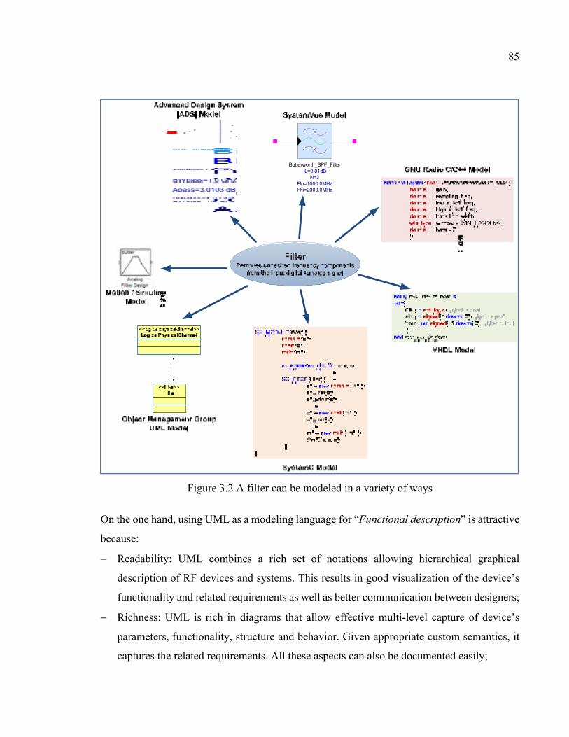
85
Fhi=2000.0MHzFlo=1000.0MHz
N=3IL=0.01dB
Butterworth_BPF_Filter
Figure 3.2 A filter can be modeled in a variety of ways
On the one hand, using UML as a modeling language for “Functional description” is attractive
because:
− Readability: UML combines a rich set of notations allowing hierarchical graphical
description of RF devices and systems. This results in good visualization of the device’s
functionality and related requirements as well as better communication between designers;
− Richness: UML is rich in diagrams that allow effective multi-level capture of device’s
parameters, functionality, structure and behavior. Given appropriate custom semantics, it
captures the related requirements. All these aspects can also be documented easily;
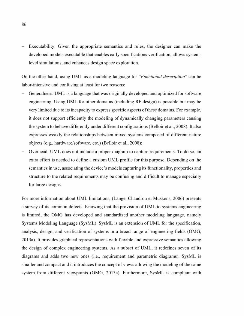
86
− Executability: Given the appropriate semantics and rules, the designer can make the
developed models executable that enables early specifications verification, allows system-
level simulations, and enhances design space exploration.
On the other hand, using UML as a modeling language for “Functional description” can be
labor-intensive and confusing at least for two reasons:
− Generalness: UML is a language that was originally developed and optimized for software
engineering. Using UML for other domains (including RF design) is possible but may be
very limited due to its incapacity to express specific aspects of these domains. For example,
it does not support efficiently the modeling of dynamically changing parameters causing
the system to behave differently under different configurations (Belloir et al., 2008). It also
expresses weakly the relationships between mixed systems composed of different-nature
objects (e.g., hardware/software, etc.) (Belloir et al., 2008);
− Overhead: UML does not include a proper diagram to capture requirements. To do so, an
extra effort is needed to define a custom UML profile for this purpose. Depending on the
semantics in use, associating the device’s models capturing its functionality, properties and
structure to the related requirements may be confusing and difficult to manage especially
for large designs.
For more information about UML limitations, (Lange, Chaudron et Muskens, 2006) presents
a survey of its common defects. Knowing that the provision of UML to systems engineering
is limited, the OMG has developed and standardized another modeling language, namely
Systems Modeling Language (SysML). SysML is an extension of UML for the specification,
analysis, design, and verification of systems in a broad range of engineering fields (OMG,
2013a). It provides graphical representations with flexible and expressive semantics allowing
the design of complex engineering systems. As a subset of UML, it redefines seven of its
diagrams and adds two new ones (i.e., requirement and parametric diagrams). SysML is
smaller and compact and it introduces the concept of views allowing the modeling of the same
system from different viewpoints (OMG, 2013a). Furthermore, SysML is compliant with
87
various standardized data interchange formats (e.g., XML41, XMI42, AP-23343, etc.) which
makes models, data and metadata exchange easy (OMG, 2013a).
Figure 3.3 Typical specifications of a GPS L1 RF filter
Considering the provision of SysML, we attempted in (Lafi et al., 2008) to model a UMTS
transceiver using the different diagrams and concepts provided within the language. This case
study allowed us to conclude that SysML is a more suitable modeling language for “Functional
Description” than UML.
For illustration purposes only, the RF filter whose specifications are given in Figure 3.3, can
be described by the SysML model in Figure 3.4. This example is not exhaustive. A complete
bandpass filter model is presented in chapter 5.
41 The Extensible Markup Language (XML) is a markup language that was standardized by the World Wide Web Consortium (W3C).
42 The XML Metadata Interchange (XMI) is an XML-based OMG standard for metadata exchange. 43 AP-233 (also known as STEP AP-233) is an ISO standard for systems engineering data representation.
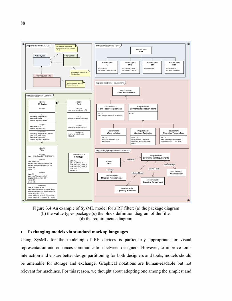
88
pkg RF Filter Model (v. 1.0)
Value Types Filter Definition
Filter Requirements
bdd [package] Filter Definition
«default»
«values»operatingTemperature: C bandwidth: MHzcenterFrequency: MHz
«weights»bandwidth: 5.0centerFrequency: 5.0
«default»referenceImpedance = 50
«values»referenceImpedance: Ohm
«weights»referenceImpedance: 2.0
«default»type = FilterType.BUTTERWORTH
«values»type: FilterType«array» passbandAttenuation: dB«array» stopbandAttenuation: dBripp le: dBorder: int
«weights»type: 1.0passbandAttenuation: 5.0stopbandAttenuation: 5.0ripp le: 3.0order: 4.0
req [package] Requirements Satisfaction
«requirement»Structure Requirements
«requirement»Environmental Requirements
«block»Filter
«satisfy»
«satisfy»
1 2
This package contains the filter requirements
This package contains the filter definit ion
This package contains the definition of units and common values
req [package] Filter Requirements
«requirement»Filter Requirements
id=”1.1”text=”smallest possible form factor”
«requirement»Water Isolation
id=”1.2.1”text=”the filter should be waterproof”
«requirement»Lightning Protection
id=”1.2.2”text=”the filter should be protected against lightn ing effects”
«requirement»Operating Temperature
id=”1.2.3”text=”operation temperature ranges from -40°C and 80°C”
«block»Port
«block»Filter
id=”1.2”
(a) (b)
(c) (d)
«unit»dimension =
«valueType»C
bdd [package] Value Types
«valueType»Real
«unit»dimension =
«valueType»MHz
«unit»dimension =
«valueType»dB
«unit»dimension =
«valueType»dBm
unit= Celsiusdimension= Temperature
unit= Milliwattdimension= Power
unit= Decibelunit= Mega_Hertzdimension= Frequency
«unit»dimension =
«enumeration»FilterType
BESSELBUTTERWORTHCHEBYSHEV_TYPE_ICHEBYSHEV_TYPE_IICUSTOMELLEPTIC
«block»RF Device
«requirement»Water Isolation
«requirement»Operating Temperature
«requirement»Lightning Protection
«derive Reqt»
«derive Reqt»
«derive Reqt»
«requirement»Environmental Requirements
«requirement»Form Factor Requirements
«constraints»operatingTemperature: Interva l [min: -5%, max: +5%] bandwidth: AbsolutecenterFrequency: Absolute
«constraints»type: Enumeration listpassbandAttenuation: Relative [±5%] stopbandAttenuation: Maximize [±5%]ripp le: Minimize [+5%]order: Minimize [max: 7] Eq: weight = order_max/order – order/order_max
«constraints»referenceImpedance: Absolute
Figure 3.4 An example of SysML model for a RF filter: (a) the package diagram (b) the value types package (c) the block definition diagram of the filter
(d) the requirements diagram
• Exchanging models via standard markup languages
Using SysML for the modeling of RF devices is particularly appropriate for visual
representation and enhances communication between designers. However, to improve tools
interaction and ensure better design partitioning for both designers and tools, models should
be amenable for storage and exchange. Graphical notations are human-readable but not
relevant for machines. For this reason, we thought about adopting one among the simplest and
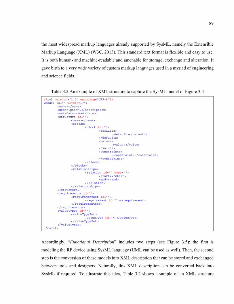
89
the most widespread markup languages already supported by SysML, namely the Extensible
Markup Language (XML) (W3C, 2013). This standard text format is flexible and easy to use.
It is both human- and machine-readable and amenable for storage, exchange and alteration. It
gave birth to a very wide variety of custom markup languages used in a myriad of engineering
and science fields.
Table 3.2 An example of XML structure to capture the SysML model of Figure 3.4
<?xml version="1.0" encoding="UTF-8"?> <model id="" version=""> <name></name> <description></description> <metadata></metadata> <structure id=""> <name></name> <blocks> <block id=""> <defaults> <default></default> </defaults> <values> <value></value> </values> <constraints> <constraint></constraint> </constraints> </block> </blocks> <relationships> <relation id="" type=""> <start></start> <end></end> </relation> </relationships> </structure> <requirements id=""> <requirementSet id=""> <requirement id=""></requirement> </requirementSet> </requirements> <valueTypes id=""> <valueTypeSet> <valueType id=""></valueType> </valueTypeSet> </valueTypes> </model>
Accordingly, “Functional Description” includes two steps (see Figure 3.5): the first is
modeling the RF device using SysML language (UML can be used as well). Then, the second
step is the conversion of these models into XML description that can be stored and exchanged
between tools and designers. Naturally, this XML description can be converted back into
SysML if required. To illustrate this idea, Table 3.2 shows a sample of an XML structure
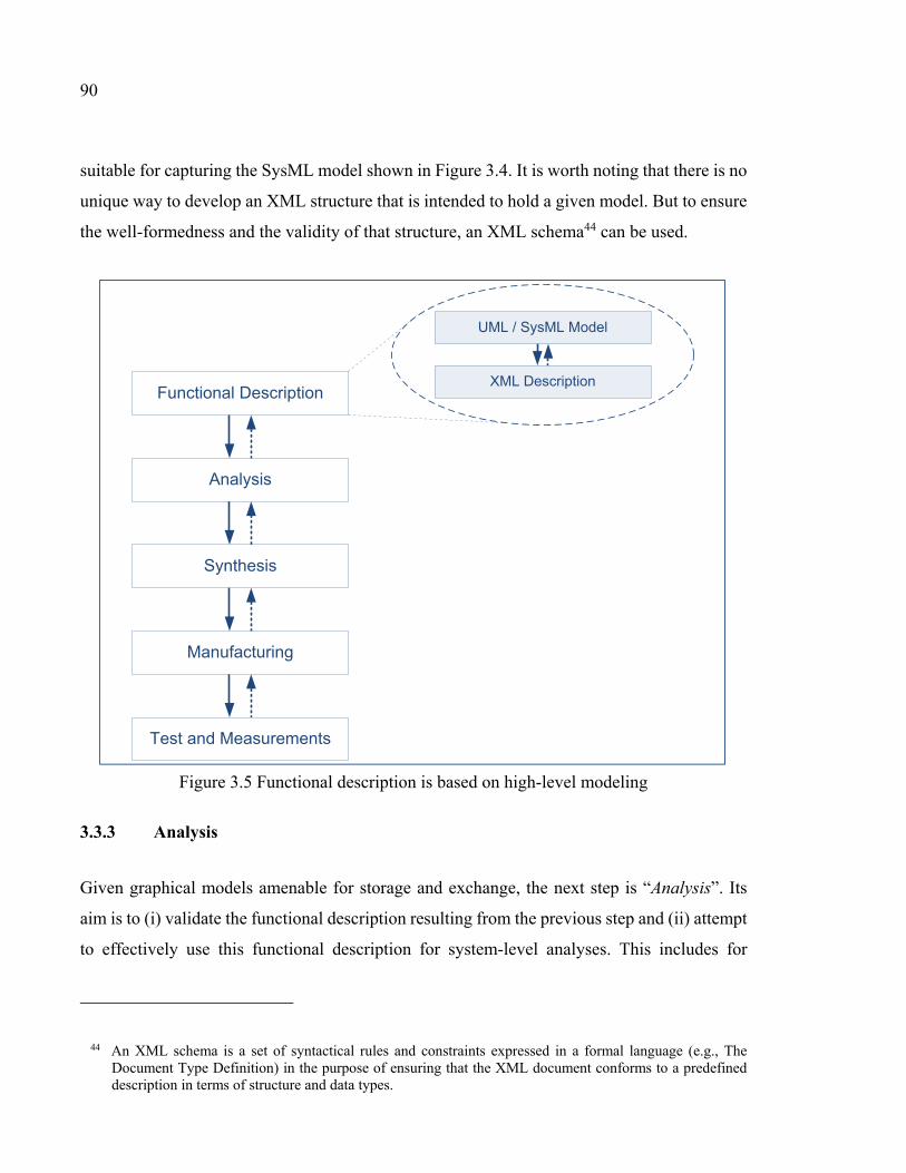
90
suitable for capturing the SysML model shown in Figure 3.4. It is worth noting that there is no
unique way to develop an XML structure that is intended to hold a given model. But to ensure
the well-formedness and the validity of that structure, an XML schema44 can be used.
Functional Description
Analysis
Synthesis
Manufacturing
Test and Measurements
XML Description
UML / SysML Model
Figure 3.5 Functional description is based on high-level modeling
3.3.3 Analysis
Given graphical models amenable for storage and exchange, the next step is “Analysis”. Its
aim is to (i) validate the functional description resulting from the previous step and (ii) attempt
to effectively use this functional description for system-level analyses. This includes for
44 An XML schema is a set of syntactical rules and constraints expressed in a formal language (e.g., The Document Type Definition) in the purpose of ensuring that the XML document conforms to a predefined description in terms of structure and data types.
91
example, the search of an initial implementation solution that matches, in part or in whole,
with the initial functional description.
• Validating the specifications through “Coherence Verification”
The process of “Coherence Verification” is based on a set of coherence rules that are used to
validate the consistency of the functional description. These rules may be embedded within the
SysML model or provided as a separate input. It aims to check out the consistency of functional
description models (including the associated XML description) and detect any eventual errors
at early design stages.
In general, the coherence rules can be subdivided into three main categories:
− Electrical consistence rules: these rules verify the relationships between the different
blocks’ values and default values45 within the SysML models (which express the various
parameters of system being designed). If two electrical parameters are assigned to
contradictory values, an error is reported. For example, this happens for filters when the
ripple value does not correspond to the specified passband attenuation (which makes the
filter not feasible because the filter’s ripple should correspond to the minimum required
passband attenuation, see detailed explanation in Figure 3.7). To easily figure out the
mathematical relationship between the various models’ parameters, we propose to map
them using a graph where every couple of parameters are related using an arrow if there is
a relationship (i.e., electrical/mathematical) linking them. This mapping results in the
Parameters’ Relationships Graph (PRG);
− Functional-level design constraints: these rules are related to the design considerations to
make at functional level in order to prevent non-feasible or poor design solutions. For
example, a Chebyshev or Elliptic filter with an even order might be refused in a 50-ohm
system because it results in an unmatched output that requires an additional matching
network to work properly (see Figure 3.7);
45 A value property in SysML semantics represents a quantity parameter that can be assigned a type and a value. Delligatti, Lenny (304). 2013. SysML Distilled: A Brief Guide to the Systems Modeling Language, First. Addison-Wesley Professional.

92
− Integrity control rules: these rules are all about the control of the definition domain,
acceptable range and type of each parameter (value property or attribute in SysML models).
For example, a power value cannot be negative. If it is assigned to a value of 100 dBW, a
warning is reported because that value is very huge and unrealistic.
In addition, we defined two levels of consistency checks in order to quantify any potential
inconsistence level:
− Warnings: this level indicates that a coherence rule has detected a minor issue within the
provided functional description that can eventually influence the design consistency at later
stages;
− Errors: a coherence rule results in an error when it detects a major inconsistency that makes
the design practically impossible to implement.
For illustration, the coherence rules corresponding to GPS filter SysML model given in Figure
3.4 are summarized in Tables 3.3, 3.4 – 3.5. Considering the following notations, the electrical
consistence rules are elaborated in the PRG shown in Figure 3.6. The corresponding
mathematical equations are given in Table 3.3.
Filter order
Bandwidth
Central Frequency
Cutoff Frequency
Stopband Edge Frequency
Ripple factor
Passband Attenuation
Stopband Attenuation
Filter Selectivity or Rejection
Reference Impedance
As shown in Figure 3.6, a subset of arrows and graph nodes express a relationship between a
subset of value properties (i.e., parameters). For example, the filter’s rejection equation (row
1 in Table 3.3) expresses the difference between the stopband attenuation and the passband
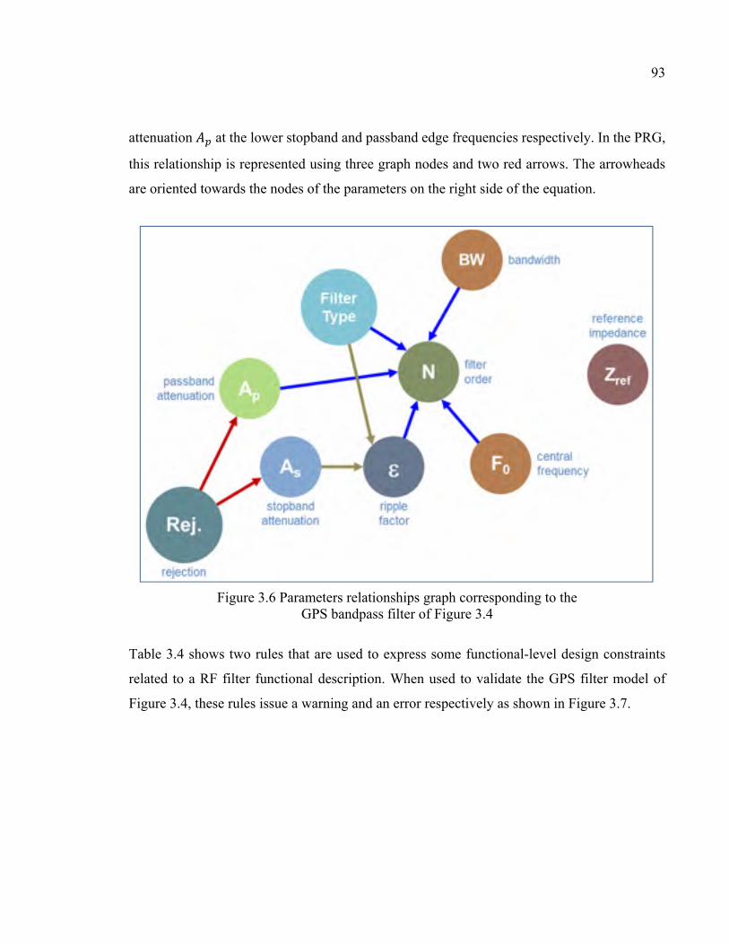
93
attenuation at the lower stopband and passband edge frequencies respectively. In the PRG,
this relationship is represented using three graph nodes and two red arrows. The arrowheads
are oriented towards the nodes of the parameters on the right side of the equation.
Figure 3.6 Parameters relationships graph corresponding to the GPS bandpass filter of Figure 3.4
Table 3.4 shows two rules that are used to express some functional-level design constraints
related to a RF filter functional description. When used to validate the GPS filter model of
Figure 3.4, these rules issue a warning and an error respectively as shown in Figure 3.7.
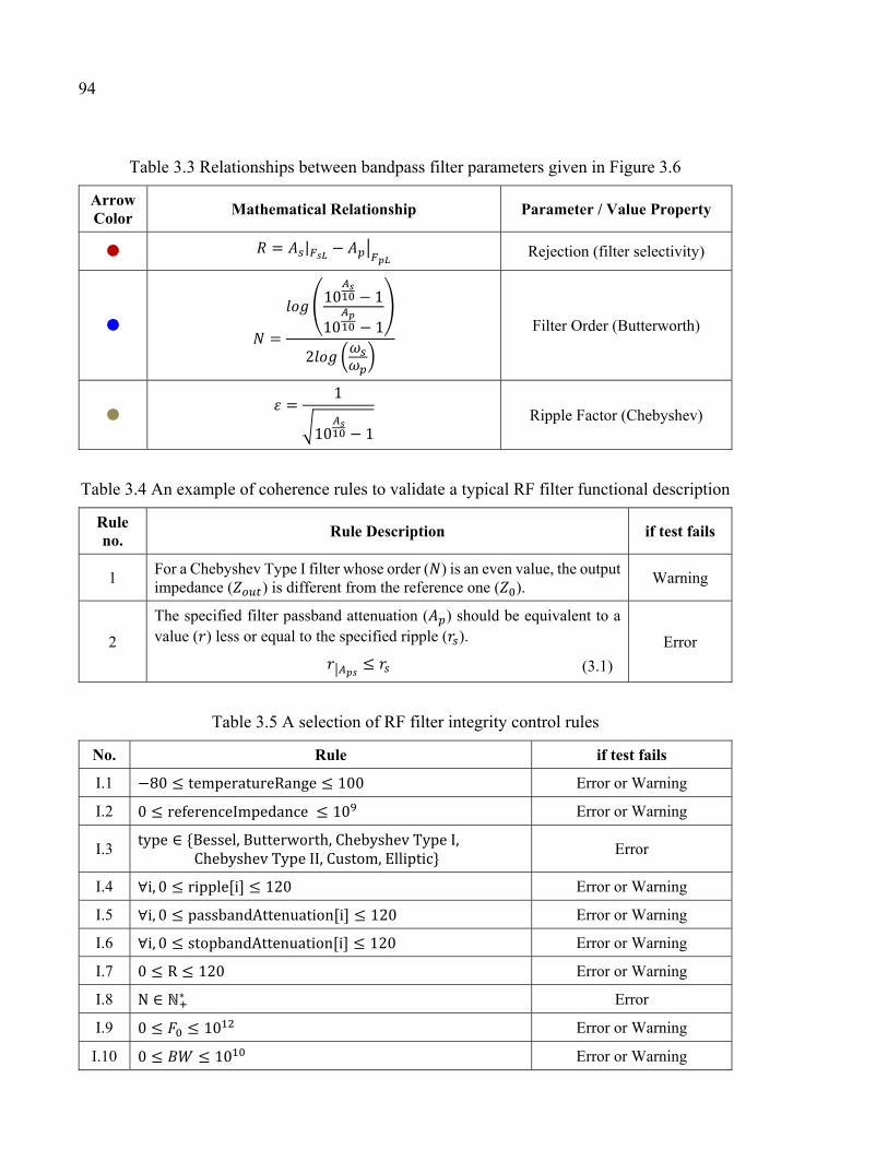
94
Table 3.3 Relationships between bandpass filter parameters given in Figure 3.6
Arrow Color
Mathematical Relationship Parameter / Value Property
= | − Rejection (filter selectivity)
= 10 − 110 − 12 Filter Order (Butterworth)
= 110 − 1
Ripple Factor (Chebyshev)
Table 3.4 An example of coherence rules to validate a typical RF filter functional description
Rule no.
Rule Description if test fails
1 For a Chebyshev Type I filter whose order ( ) is an even value, the output impedance ( ) is different from the reference one ( ).
Warning
2
The specified filter passband attenuation ( ) should be equivalent to a value ( ) less or equal to the specified ripple ( ). ≤ (3.1)
Error
Table 3.5 A selection of RF filter integrity control rules
No. Rule if test fails
I.1 −80 ≤ temperatureRange ≤ 100 Error or Warning
I.2 0 ≤ referenceImpedance ≤ 10 Error or Warning
I.3 type ∈ Bessel,Butterworth,ChebyshevTypeI,ChebyshevTypeII,Custom,Elliptic Error
I.4 ∀i, 0 ≤ ripple[i] ≤ 120 Error or Warning
I.5 ∀i, 0 ≤ passbandAttenuation[i] ≤ 120 Error or Warning
I.6 ∀i, 0 ≤ stopbandAttenuation[i] ≤ 120 Error or Warning
I.7 0 ≤ R ≤ 120 Error or Warning
I.8 N ∈ ℕ∗ Error
I.9 0 ≤ ≤ 10 Error or Warning
I.10 0 ≤ ≤ 10 Error or Warning

95
Finally, the integrity control rules defining the range of values accepted for each value
parameter of the SysML model are enumerated in Table 3.4.
Figure 3.7 Example of coherence rules to validate a RF filter functional description: (a)46 A warning results from a rule that detects a minor consistency issue, while (b)47 an error indicates a major incoherence
that makes the design not feasible
• Enhancing system-level analysis
One of the goals of functional description is to enhance design space exploration by enabling
effective system-level analyses. Given the appropriate tools and depending on the intended
functionality, the functional description previously checked for coherence can be immediately
46 and denote the passband and stopband attenuation respectively. denotes the filter’s order and denotes the output impedance.
47 and denote the ripple factor and the specified ripple respectively while and denote the insertion loss and passband attenuation respectively.
96
used to carry out a number of analyses that result in an initial design solution. This solution
can be a good entry to the following design stages (especially “Synthesis”. Nevertheless, at this
early step, it should be independent from technology in order to allow more flexibility in the
remaining design process.
To illustrate this concept, Figure 3.8.a shows the schematic of an ideal lumped-component
(LC) circuit that implements the previously functional description. This LC network is ideal
and independent from technology. Figure 3.8.b, c and d show various simulations that can be
carried out in order to evaluate its performance. The designer can tune and adjust this solution
for an optimized response. It can also be used in the following “Synthesis” step in order to take
into account more considerations (e.g., technology properties).
In summary, the “Analysis” step encompasses two sub-steps as shown in Figure 3.9:
“Coherence Verification” that validates the functional description and “Performance
Simulation” that uses the verified functional description to look for a technology-independent
design solution.
3.3.4 Synthesis
After the validation of specifications and the selection of an initial (i.e., most likely system-
level) solution, the designer can undertake the development of a more elaborated
implementation that takes into account physical details such as the technology information and
constraints (e.g., design rules). This includes the incremental refinement and optimization of
the solution as well as the assessment of its performance. To do so, we propose a design stage,
namely “Synthesis” that is subdivided into three consecutive sub-steps: “Granularity
Refinement”, “Technology Mapping” and “Performance Simulation” respectively.
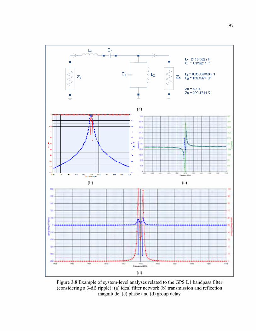
97
(a)
(b) (c)
(d)
Figure 3.8 Example of system-level analyses related to the GPS L1 bandpass filter (considering a 3-dB ripple): (a) ideal filter network (b) transmission and reflection
magnitude, (c) phase and (d) group delay
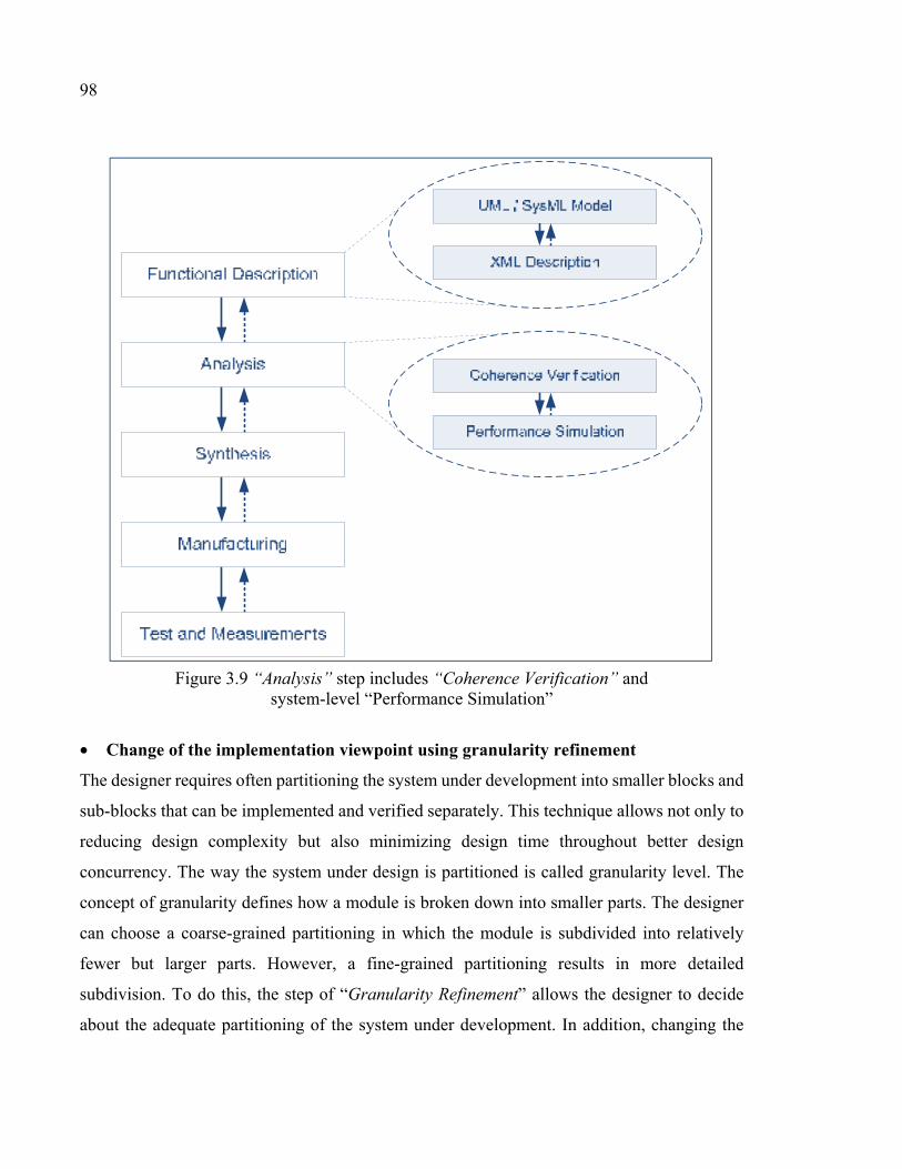
98
Figure 3.9 “Analysis” step includes “Coherence Verification” and system-level “Performance Simulation”
• Change of the implementation viewpoint using granularity refinement
The designer requires often partitioning the system under development into smaller blocks and
sub-blocks that can be implemented and verified separately. This technique allows not only to
reducing design complexity but also minimizing design time throughout better design
concurrency. The way the system under design is partitioned is called granularity level. The
concept of granularity defines how a module is broken down into smaller parts. The designer
can choose a coarse-grained partitioning in which the module is subdivided into relatively
fewer but larger parts. However, a fine-grained partitioning results in more detailed
subdivision. To do this, the step of “Granularity Refinement” allows the designer to decide
about the adequate partitioning of the system under development. In addition, changing the
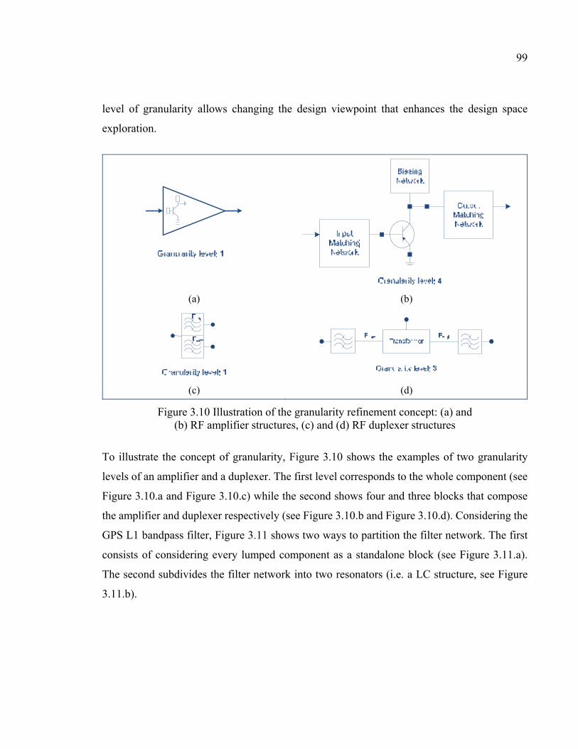
99
level of granularity allows changing the design viewpoint that enhances the design space
exploration.
(a) (b)
(c) (d)
Figure 3.10 Illustration of the granularity refinement concept: (a) and (b) RF amplifier structures, (c) and (d) RF duplexer structures
To illustrate the concept of granularity, Figure 3.10 shows the examples of two granularity
levels of an amplifier and a duplexer. The first level corresponds to the whole component (see
Figure 3.10.a and Figure 3.10.c) while the second shows four and three blocks that compose
the amplifier and duplexer respectively (see Figure 3.10.b and Figure 3.10.d). Considering the
GPS L1 bandpass filter, Figure 3.11 shows two ways to partition the filter network. The first
consists of considering every lumped component as a standalone block (see Figure 3.11.a).
The second subdivides the filter network into two resonators (i.e. a LC structure, see Figure
3.11.b).
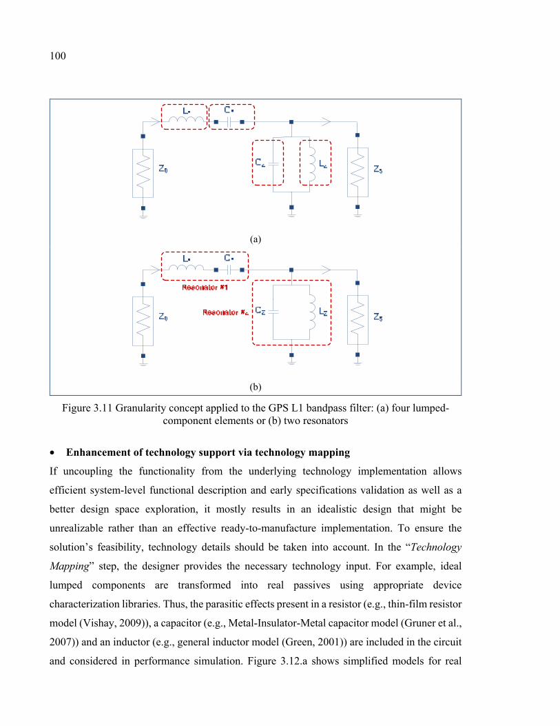
100
(a)
(b)
Figure 3.11 Granularity concept applied to the GPS L1 bandpass filter: (a) four lumped-component elements or (b) two resonators
• Enhancement of technology support via technology mapping
If uncoupling the functionality from the underlying technology implementation allows
efficient system-level functional description and early specifications validation as well as a
better design space exploration, it mostly results in an idealistic design that might be
unrealizable rather than an effective ready-to-manufacture implementation. To ensure the
solution’s feasibility, technology details should be taken into account. In the “Technology
Mapping” step, the designer provides the necessary technology input. For example, ideal
lumped components are transformed into real passives using appropriate device
characterization libraries. Thus, the parasitic effects present in a resistor (e.g., thin-film resistor
model (Vishay, 2009)), a capacitor (e.g., Metal-Insulator-Metal capacitor model (Gruner et al.,
2007)) and an inductor (e.g., general inductor model (Green, 2001)) are included in the circuit
and considered in performance simulation. Figure 3.12.a shows simplified models for real
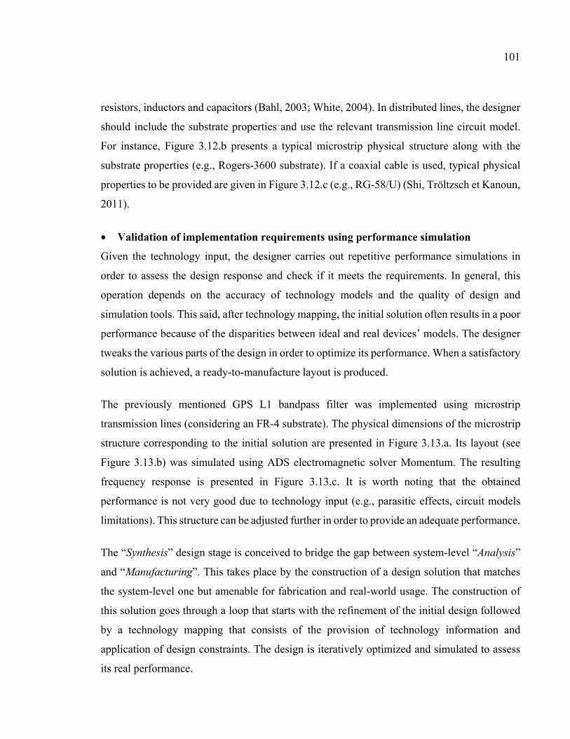
101
resistors, inductors and capacitors (Bahl, 2003; White, 2004). In distributed lines, the designer
should include the substrate properties and use the relevant transmission line circuit model.
For instance, Figure 3.12.b presents a typical microstrip physical structure along with the
substrate properties (e.g., Rogers-3600 substrate). If a coaxial cable is used, typical physical
properties to be provided are given in Figure 3.12.c (e.g., RG-58/U) (Shi, Tröltzsch et Kanoun,
2011).
• Validation of implementation requirements using performance simulation
Given the technology input, the designer carries out repetitive performance simulations in
order to assess the design response and check if it meets the requirements. In general, this
operation depends on the accuracy of technology models and the quality of design and
simulation tools. This said, after technology mapping, the initial solution often results in a poor
performance because of the disparities between ideal and real devices’ models. The designer
tweaks the various parts of the design in order to optimize its performance. When a satisfactory
solution is achieved, a ready-to-manufacture layout is produced.
The previously mentioned GPS L1 bandpass filter was implemented using microstrip
transmission lines (considering an FR-4 substrate). The physical dimensions of the microstrip
structure corresponding to the initial solution are presented in Figure 3.13.a. Its layout (see
Figure 3.13.b) was simulated using ADS electromagnetic solver Momentum. The resulting
frequency response is presented in Figure 3.13.c. It is worth noting that the obtained
performance is not very good due to technology input (e.g., parasitic effects, circuit models
limitations). This structure can be adjusted further in order to provide an adequate performance.
The “Synthesis” design stage is conceived to bridge the gap between system-level “Analysis”
and “Manufacturing”. This takes place by the construction of a design solution that matches
the system-level one but amenable for fabrication and real-world usage. The construction of
this solution goes through a loop that starts with the refinement of the initial design followed
by a technology mapping that consists of the provision of technology information and
application of design constraints. The design is iteratively optimized and simulated to assess
its real performance.
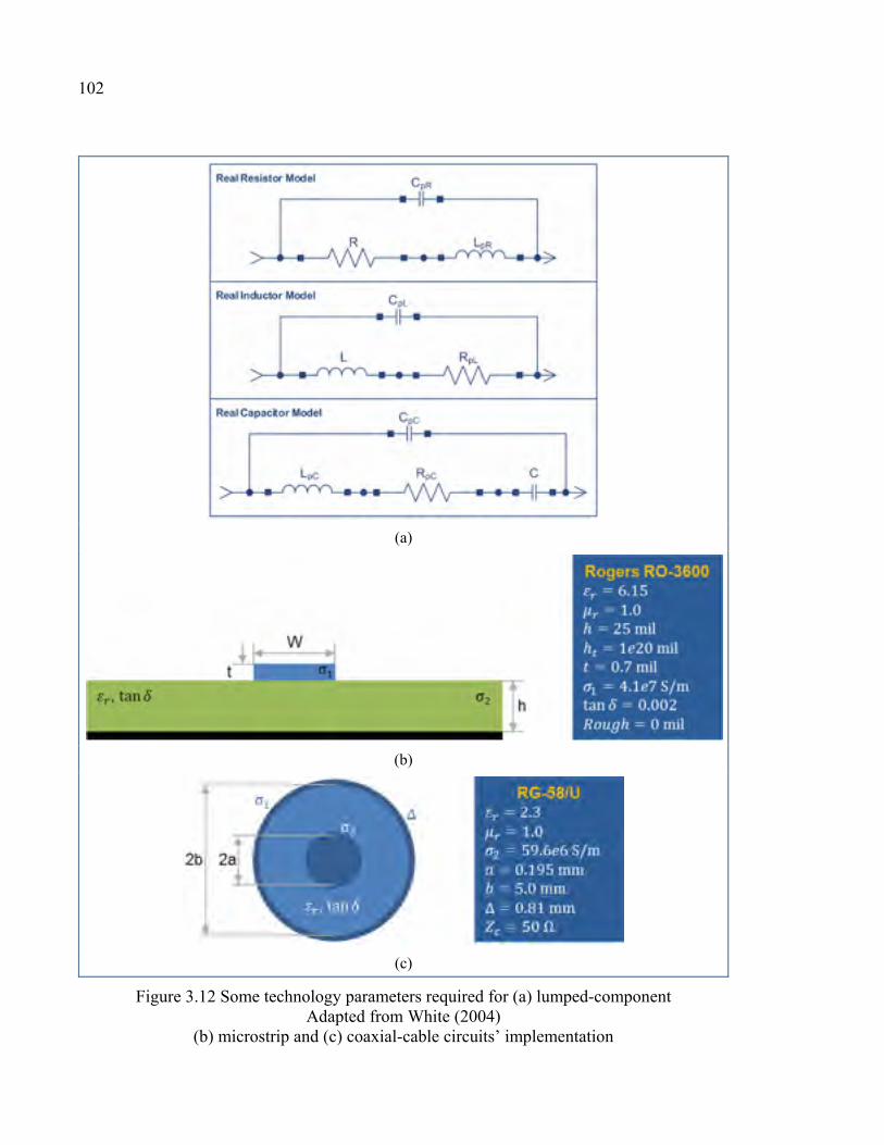
102
(a)
(b)
(c)
Figure 3.12 Some technology parameters required for (a) lumped-component Adapted from White (2004)
(b) microstrip and (c) coaxial-cable circuits’ implementation
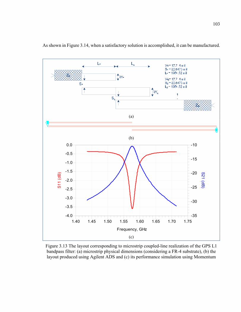
103
As shown in Figure 3.14, when a satisfactory solution is accomplished, it can be manufactured.
(a)
(b)
(c)
Figure 3.13 The layout corresponding to microstrip coupled-line realization of the GPS L1 bandpass filter: (a) microstrip physical dimensions (considering a FR-4 substrate), (b) the layout produced using Agilent ADS and (c) its performance simulation using Momentum
1.45 1.50 1.55 1.60 1.65 1.701.40 1.75
-3.5
-3.0
-2.5
-2.0
-1.5
-1.0
-0.5
-4.0
0.0
-30
-25
-20
-15
-35
-10
Frequency, GHz
S1
1 (
dB
) S2
1 (d
B)
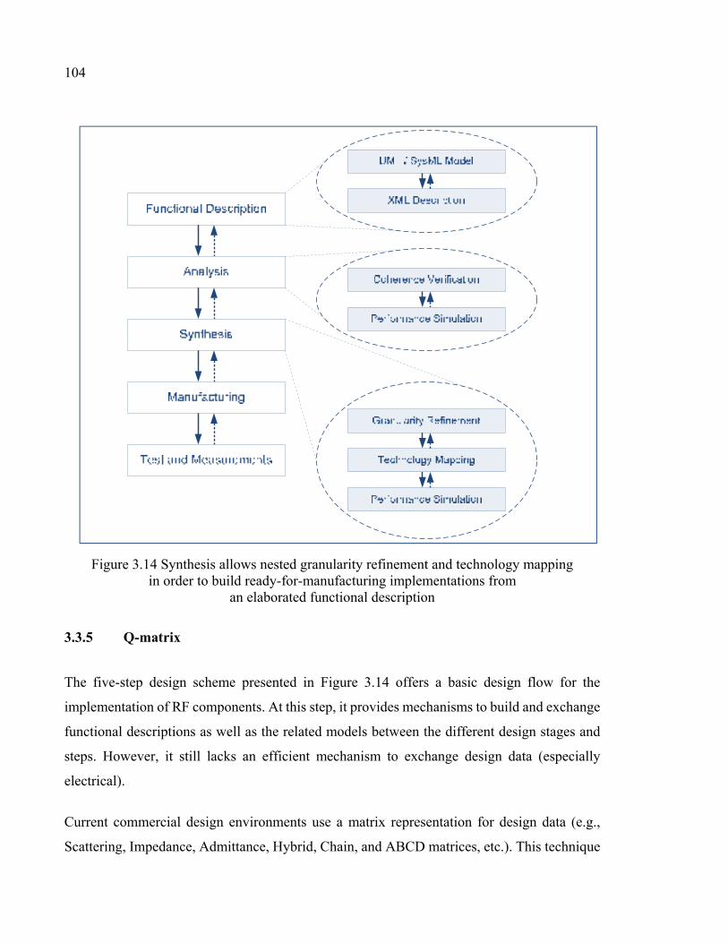
104
Figure 3.14 Synthesis allows nested granularity refinement and technology mapping in order to build ready-for-manufacturing implementations from
an elaborated functional description
3.3.5 Q-matrix
The five-step design scheme presented in Figure 3.14 offers a basic design flow for the
implementation of RF components. At this step, it provides mechanisms to build and exchange
functional descriptions as well as the related models between the different design stages and
steps. However, it still lacks an efficient mechanism to exchange design data (especially
electrical).
Current commercial design environments use a matrix representation for design data (e.g.,
Scattering, Impedance, Admittance, Hybrid, Chain, and ABCD matrices, etc.). This technique
105
is widely adopted in electrical engineering and used not only in EDA tools but also by hardware
test and measurement instrumentation. Nevertheless, it suffers from a number of limitations:
− Absence of representation uniformity: Since RF components are of different natures (e.g.,
linear/nonlinear, passive/active, etc.), there is no unique matrix form to capture the
behavior of all of them in a uniform way. For instance, to capture the DC operating points
of an amplifier, I-V curves48 are used while its small-signal transfer parameters (e.g.,
voltage and current gain, linear noise, etc.) are captured using different types of matrices
(including scattering parameters). However, its nonlinear response (e.g., intermodulation
products, gain compression, etc.) is captured using various tabular representations;
− Limited representation scope: The matrix representation (especially scattering parameters,
aka S-matrix) is limited to the same frequency at all ports. As such components such as
mixers are not characterized by S-matrix but rather a mix of reflection, conversion and
leakage coefficients. Similarly, sources and oscillators which include DC ports are difficult
to capture their response using this technique given that S-matrix is defined only for RF
ports;
− A myriad of data file formats: The design of a RF component requires numerous
simulations. Most types of simulations are captured in different ways. To exchange this
data, a myriad of file formats are used by commercial RF design packages. Some of them
are proprietary. Others are standardized. For example, AWR Microwave Office uses DC-
IV format files to import and export DC simulation data (National Instruments, 2014).
Agilent ADS uses its own TIM files for time-domain data and PDF format for user-defined,
piece-wise uncorrelated linear probability density function data (Agilent, 2005). It uses
also IMT files for mixer intermodulation product tables, and P2D ones for two-port large-
signal power-independent parameters (Agilent, 2005). In addition, both software
environments use standardized formats such as Touchstone49 (for scattering parameters),
48 An I-V curve is a current-voltage characteristic relationship between the electric current and the corresponding voltage respectively measured through and at the edges of an electrical device (e.g. transistor).
49 Touchstone (aka SnP files) is a standard file format for the storage and exchange of n-port network parameters (e.g., S/H/Z/Y) and two-port linear noise.
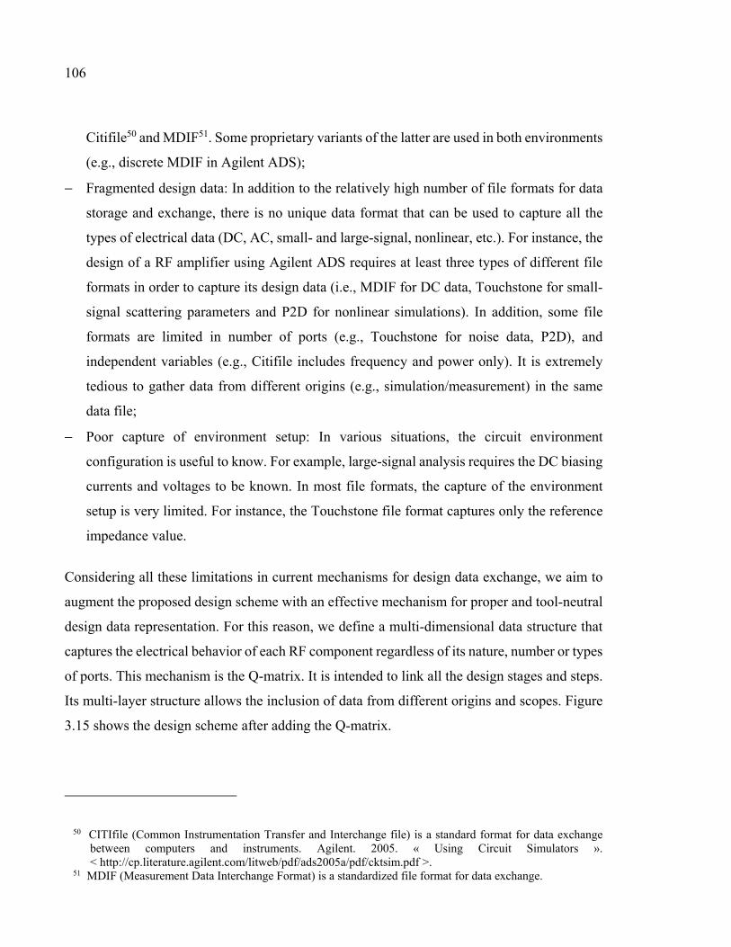
106
Citifile50 and MDIF51. Some proprietary variants of the latter are used in both environments
(e.g., discrete MDIF in Agilent ADS);
− Fragmented design data: In addition to the relatively high number of file formats for data
storage and exchange, there is no unique data format that can be used to capture all the
types of electrical data (DC, AC, small- and large-signal, nonlinear, etc.). For instance, the
design of a RF amplifier using Agilent ADS requires at least three types of different file
formats in order to capture its design data (i.e., MDIF for DC data, Touchstone for small-
signal scattering parameters and P2D for nonlinear simulations). In addition, some file
formats are limited in number of ports (e.g., Touchstone for noise data, P2D), and
independent variables (e.g., Citifile includes frequency and power only). It is extremely
tedious to gather data from different origins (e.g., simulation/measurement) in the same
data file;
− Poor capture of environment setup: In various situations, the circuit environment
configuration is useful to know. For example, large-signal analysis requires the DC biasing
currents and voltages to be known. In most file formats, the capture of the environment
setup is very limited. For instance, the Touchstone file format captures only the reference
impedance value.
Considering all these limitations in current mechanisms for design data exchange, we aim to
augment the proposed design scheme with an effective mechanism for proper and tool-neutral
design data representation. For this reason, we define a multi-dimensional data structure that
captures the electrical behavior of each RF component regardless of its nature, number or types
of ports. This mechanism is the Q-matrix. It is intended to link all the design stages and steps.
Its multi-layer structure allows the inclusion of data from different origins and scopes. Figure
3.15 shows the design scheme after adding the Q-matrix.
50 CITIfile (Common Instrumentation Transfer and Interchange file) is a standard format for data exchange between computers and instruments. Agilent. 2005. « Using Circuit Simulators ». < http://cp.literature.agilent.com/litweb/pdf/ads2005a/pdf/cktsim.pdf >.
51 MDIF (Measurement Data Interchange Format) is a standardized file format for data exchange.
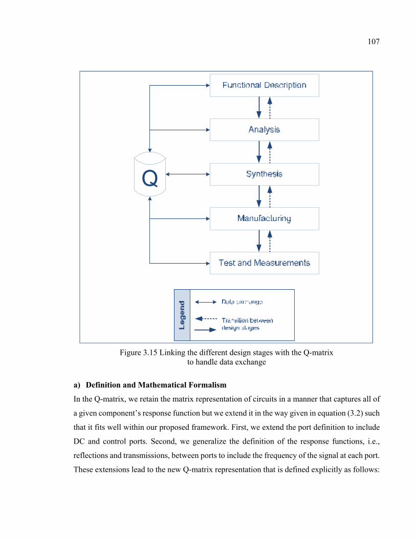
107
Figure 3.15 Linking the different design stages with the Q-matrix to handle data exchange
a) Definition and Mathematical Formalism
In the Q-matrix, we retain the matrix representation of circuits in a manner that captures all of
a given component’s response function but we extend it in the way given in equation (3.2) such
that it fits well within our proposed framework. First, we extend the port definition to include
DC and control ports. Second, we generalize the definition of the response functions, i.e.,
reflections and transmissions, between ports to include the frequency of the signal at each port.
These extensions lead to the new Q-matrix representation that is defined explicitly as follows:
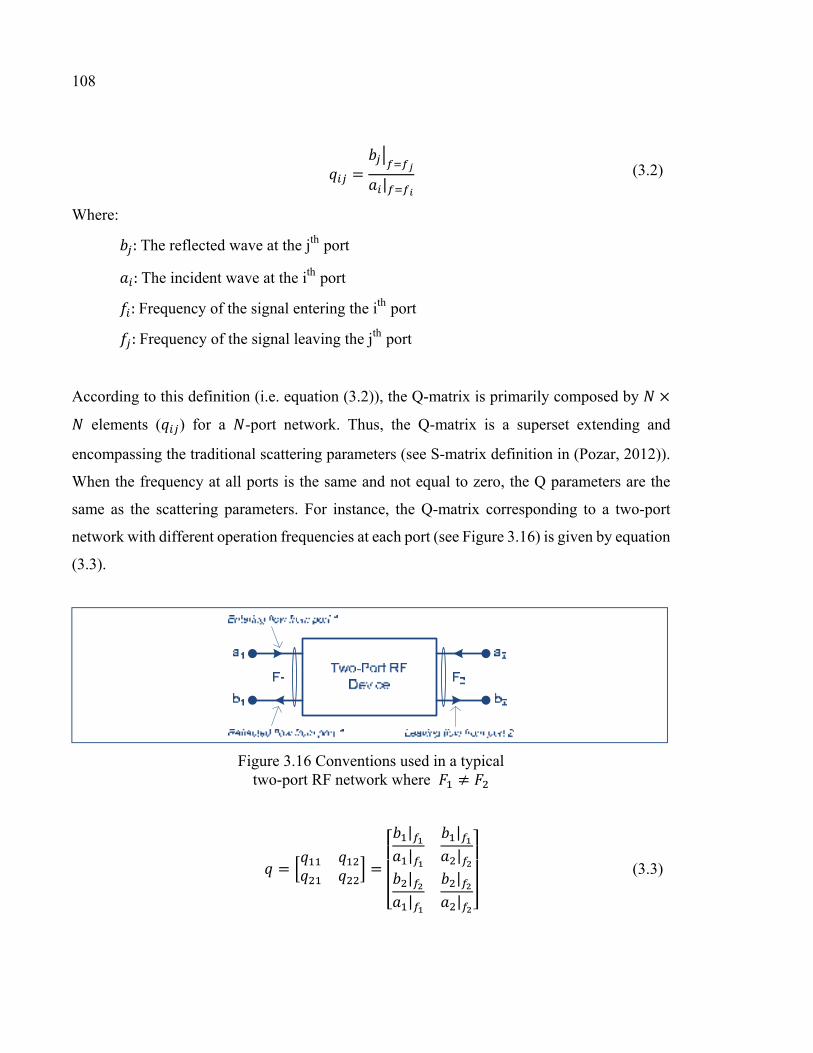
108
= | (3.2)
Where: :The reflected wave at the jth port :The incident wave at the ith port :Frequency of the signal entering the ith port :Frequency of the signal leaving the jth port
According to this definition (i.e. equation (3.2)), the Q-matrix is primarily composed by × elements ( ) for a -port network. Thus, the Q-matrix is a superset extending and
encompassing the traditional scattering parameters (see S-matrix definition in (Pozar, 2012)).
When the frequency at all ports is the same and not equal to zero, the Q parameters are the
same as the scattering parameters. For instance, the Q-matrix corresponding to a two-port
network with different operation frequencies at each port (see Figure 3.16) is given by equation
(3.3).
Figure 3.16 Conventions used in a typical two-port RF network where ≠
= = || |||| || (3.3)
109
The definition given in equations (3.2) and (3.3) generalizes the traditional incident and
reflected wave ratios regardless of the operating frequency at each port. However, this is not
enough to cover more than one independent variable. For this reason, we introduce a broader
definition, that is , , ,
, given in equation (3.4). It is a sparse matrix that includes the Q-
matrix’s basic elements in function of four independent variables (i.e. frequency, power,
temperature and aging time). As shown in Figure 3.17, the extended data structure , , ,
is
construction that is able to hold this multidimensional data.
, , , = × × × × (3.4)
Where: :time (aging):Temperature:Power:Frequency:Total number of ports :Number of time steps:Number of temperature points:Number of power points:Number of frequency points
b) Data File Format
Given the generalized data structure , , ,
, the next step is to define a data file format that
holds the design electrical data and allows the storage and exchange of a minimum set of
environment setup information. For this reason, we have selected again XML to develop that
structure. In addition to the reasons we presented in section 3.3.2 to justify the choice of XML,
we note that this language is being gradually introduced in state-of-the-art commercial design
packages for RF and microwave circuits for data and/or circuit topology exchange (e.g.,
Agilent Genesys (Agilent, 2010a) and SystemVue (Agilent, 2010b)).
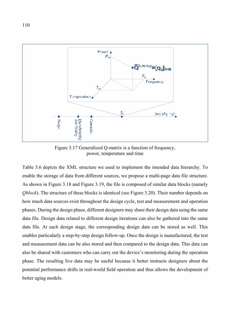
110
Figure 3.17 Generalized Q-matrix is a function of frequency, power, temperature and time
Table 3.6 depicts the XML structure we used to implement the intended data hierarchy. To
enable the storage of data from different sources, we propose a multi-page data file structure.
As shown in Figure 3.18 and Figure 3.19, the file is composed of similar data blocks (namely
Qblock). The structure of these blocks is identical (see Figure 3.20). Their number depends on
how much data sources exist throughout the design cycle, test and measurement and operation
phases. During the design phase, different designers may share their design data using the same
data file. Design data related to different design iterations can also be gathered into the same
data file. At each design stage, the corresponding design data can be stored as well. This
enables particularly a step-by-step design follow-up. Once the design is manufactured, the test
and measurement data can be also stored and then compared to the design data. This data can
also be shared with customers who can carry out the device’s monitoring during the operation
phase. The resulting live data may be useful because it better instructs designers about the
potential performance drifts in real-world field operation and thus allows the development of
better aging models.
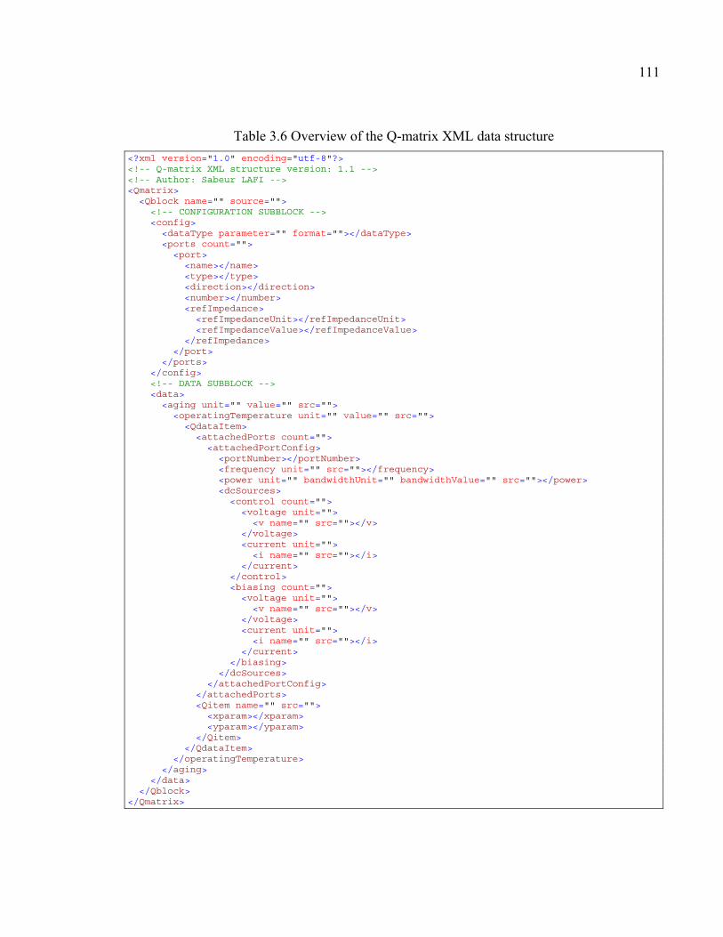
111
Table 3.6 Overview of the Q-matrix XML data structure
<?xml version="1.0" encoding="utf-8"?> <!-- Q-matrix XML structure version: 1.1 --> <!-- Author: Sabeur LAFI --> <Qmatrix> <Qblock name="" source=""> <!-- CONFIGURATION SUBBLOCK --> <config> <dataType parameter="" format=""></dataType> <ports count=""> <port> <name></name> <type></type> <direction></direction> <number></number> <refImpedance> <refImpedanceUnit></refImpedanceUnit> <refImpedanceValue></refImpedanceValue> </refImpedance> </port> </ports> </config> <!-- DATA SUBBLOCK --> <data> <aging unit="" value="" src=""> <operatingTemperature unit="" value="" src=""> <QdataItem> <attachedPorts count=""> <attachedPortConfig> <portNumber></portNumber> <frequency unit="" src=""></frequency> <power unit="" bandwidthUnit="" bandwidthValue="" src=""></power> <dcSources> <control count=""> <voltage unit=""> <v name="" src=""></v> </voltage> <current unit=""> <i name="" src=""></i> </current> </control> <biasing count=""> <voltage unit=""> <v name="" src=""></v> </voltage> <current unit=""> <i name="" src=""></i> </current> </biasing> </dcSources> </attachedPortConfig> </attachedPorts> <Qitem name="" src=""> <xparam></xparam> <yparam></yparam> </Qitem> </QdataItem> </operatingTemperature> </aging> </data> </Qblock> </Qmatrix>
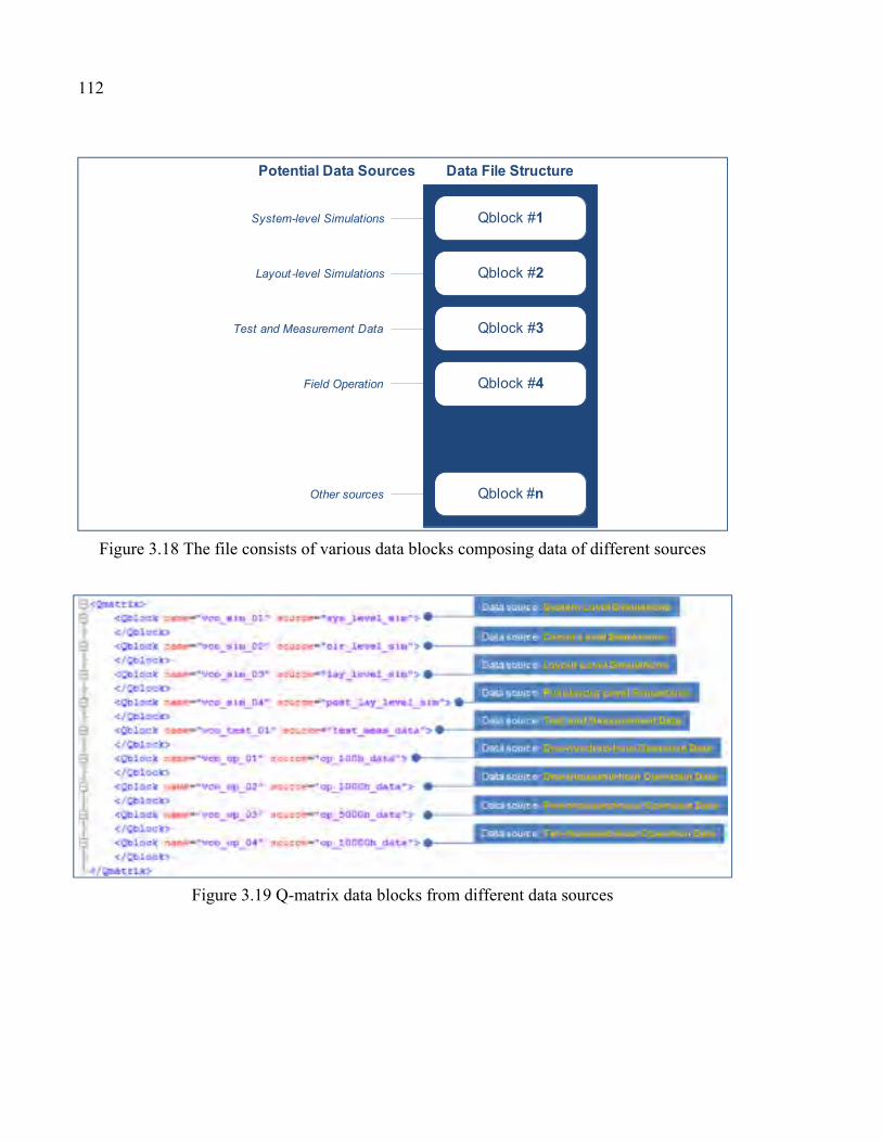
112
Qblock #1
Qblock #2
Qblock #3
Qblock #4
Qblock #n
.
.
.
System-level Simulations
Layout-level Simulations
Test and Measurement Data
Field Operation
Data File StructurePotential Data Sources
Other sources
Figure 3.18 The file consists of various data blocks composing data of different sources
Figure 3.19 Q-matrix data blocks from different data sources
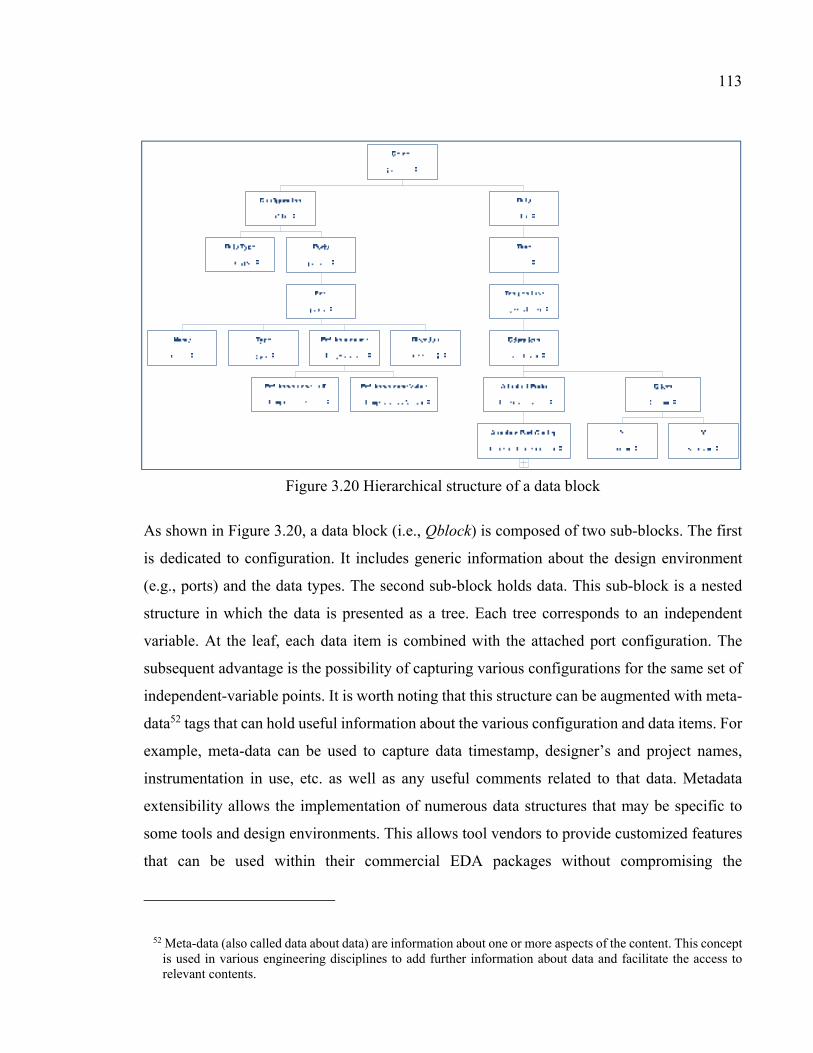
113
Figure 3.20 Hierarchical structure of a data block
As shown in Figure 3.20, a data block (i.e., Qblock) is composed of two sub-blocks. The first
is dedicated to configuration. It includes generic information about the design environment
(e.g., ports) and the data types. The second sub-block holds data. This sub-block is a nested
structure in which the data is presented as a tree. Each tree corresponds to an independent
variable. At the leaf, each data item is combined with the attached port configuration. The
subsequent advantage is the possibility of capturing various configurations for the same set of
independent-variable points. It is worth noting that this structure can be augmented with meta-
data52 tags that can hold useful information about the various configuration and data items. For
example, meta-data can be used to capture data timestamp, designer’s and project names,
instrumentation in use, etc. as well as any useful comments related to that data. Metadata
extensibility allows the implementation of numerous data structures that may be specific to
some tools and design environments. This allows tool vendors to provide customized features
that can be used within their commercial EDA packages without compromising the
52 Meta-data (also called data about data) are information about one or more aspects of the content. This concept is used in various engineering disciplines to add further information about data and facilitate the access to relevant contents.
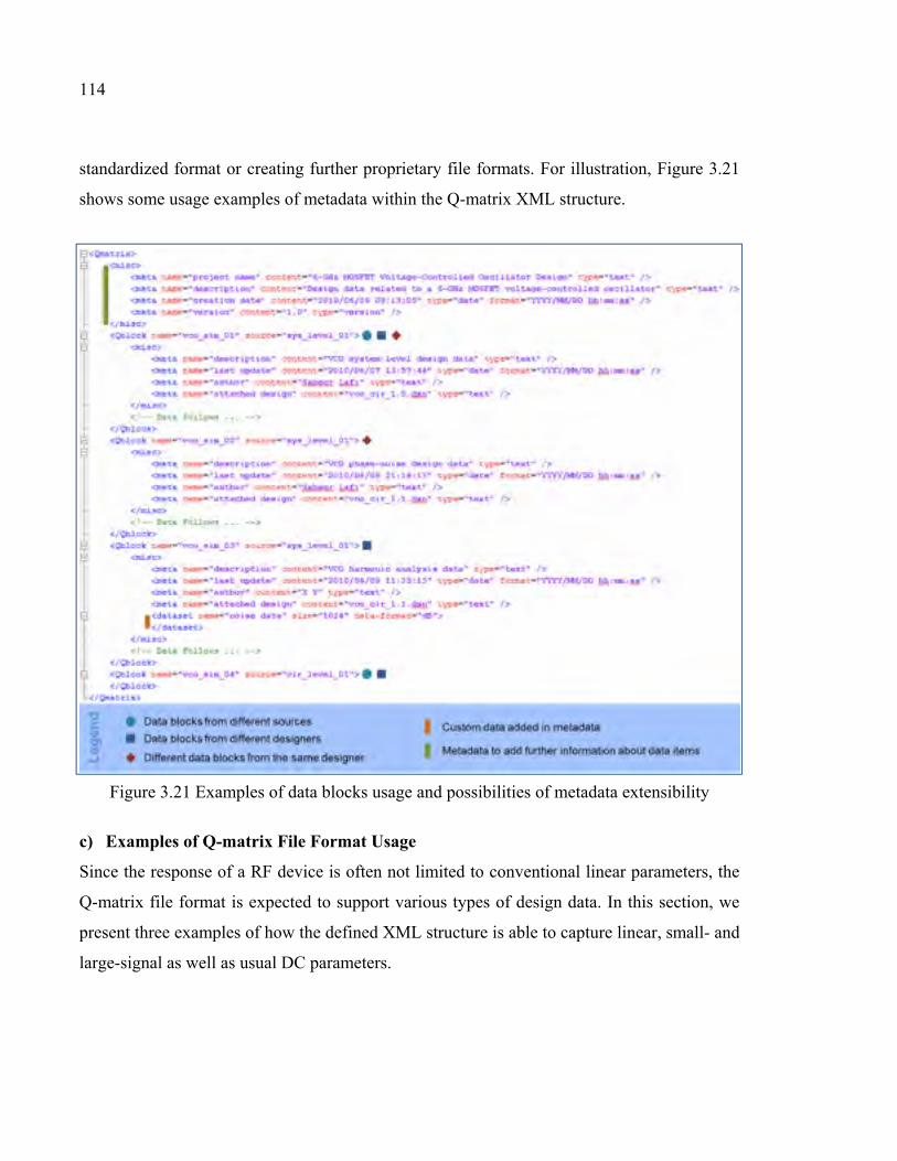
114
standardized format or creating further proprietary file formats. For illustration, Figure 3.21
shows some usage examples of metadata within the Q-matrix XML structure.
Figure 3.21 Examples of data blocks usage and possibilities of metadata extensibility
c) Examples of Q-matrix File Format Usage
Since the response of a RF device is often not limited to conventional linear parameters, the
Q-matrix file format is expected to support various types of design data. In this section, we
present three examples of how the defined XML structure is able to capture linear, small- and
large-signal as well as usual DC parameters.
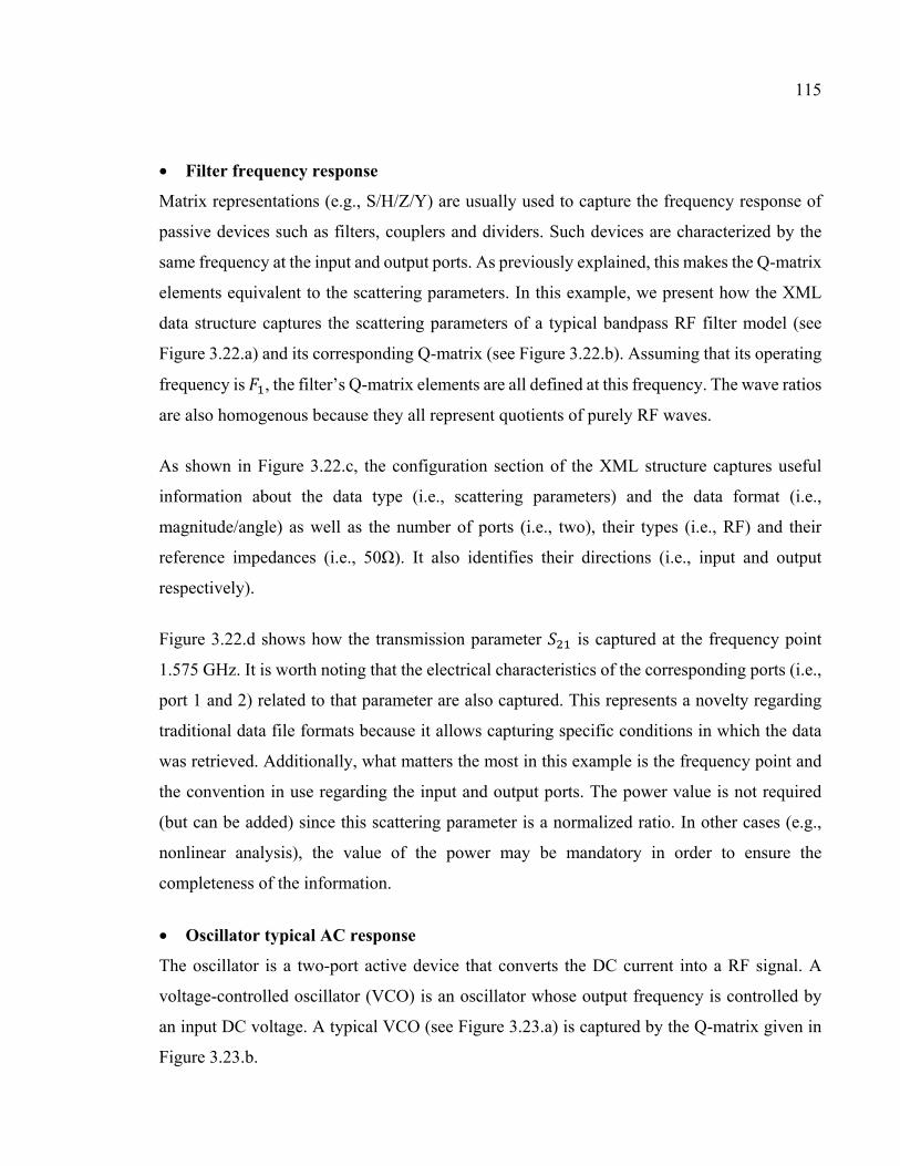
115
• Filter frequency response
Matrix representations (e.g., S/H/Z/Y) are usually used to capture the frequency response of
passive devices such as filters, couplers and dividers. Such devices are characterized by the
same frequency at the input and output ports. As previously explained, this makes the Q-matrix
elements equivalent to the scattering parameters. In this example, we present how the XML
data structure captures the scattering parameters of a typical bandpass RF filter model (see
Figure 3.22.a) and its corresponding Q-matrix (see Figure 3.22.b). Assuming that its operating
frequency is , the filter’s Q-matrix elements are all defined at this frequency. The wave ratios
are also homogenous because they all represent quotients of purely RF waves.
As shown in Figure 3.22.c, the configuration section of the XML structure captures useful
information about the data type (i.e., scattering parameters) and the data format (i.e.,
magnitude/angle) as well as the number of ports (i.e., two), their types (i.e., RF) and their
reference impedances (i.e., 50Ω). It also identifies their directions (i.e., input and output
respectively).
Figure 3.22.d shows how the transmission parameter is captured at the frequency point
1.575 GHz. It is worth noting that the electrical characteristics of the corresponding ports (i.e.,
port 1 and 2) related to that parameter are also captured. This represents a novelty regarding
traditional data file formats because it allows capturing specific conditions in which the data
was retrieved. Additionally, what matters the most in this example is the frequency point and
the convention in use regarding the input and output ports. The power value is not required
(but can be added) since this scattering parameter is a normalized ratio. In other cases (e.g.,
nonlinear analysis), the value of the power may be mandatory in order to ensure the
completeness of the information.
• Oscillator typical AC response
The oscillator is a two-port active device that converts the DC current into a RF signal. A
voltage-controlled oscillator (VCO) is an oscillator whose output frequency is controlled by
an input DC voltage. A typical VCO (see Figure 3.23.a) is captured by the Q-matrix given in
Figure 3.23.b.
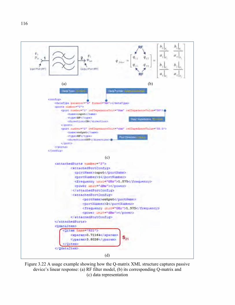
116
(a) (b)
(c)
(d)
Figure 3.22 A usage example showing how the Q-matrix XML structure captures passive device’s linear response: (a) RF filter model, (b) its corresponding Q-matrix and
(c) data representation
117
Unlike the filter’s, the presence of an input DC port results in a 2 × 2 Q-matrix where only
is purely RF. represents a quotient of locally measured DC voltage magnitudes rather than
pure waves ratio. Nevertheless, and are ratios of pure RF wave and DC voltage. These
two coefficients can be interpreted as leakage coefficients from DC to RF and RF to DC
respectively. This said, Figure 3.23.c shows an example of voltage-controlled circuit based on
a BJT53 transistor (type NPN). The VCO generates an analog signal represented by the voltage ( ) = . This output voltage depends on the input small-signal signal as well
as the constant biasing voltage .
(a) (b)
(c)
Figure 3.23 VCO’s Q-matrix XML structure: (a) A voltage-controlled oscillator model, (b) its formal Q-matrix, (c) an example of a VCO circuit
53 A Bipolar Junction Transistor (BJT) denotes a family of transistors that operates due to the interaction between three layers of two semiconductor types, one is positively-doped (i.e., P) and the other is negatively-doped (i.e., N).
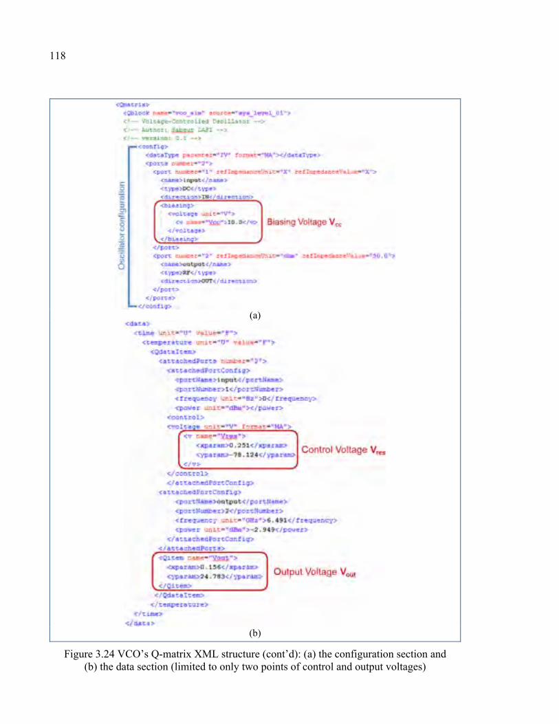
118
(a)
(b)
Figure 3.24 VCO’s Q-matrix XML structure (cont’d): (a) the configuration section and (b) the data section (limited to only two points of control and output voltages)
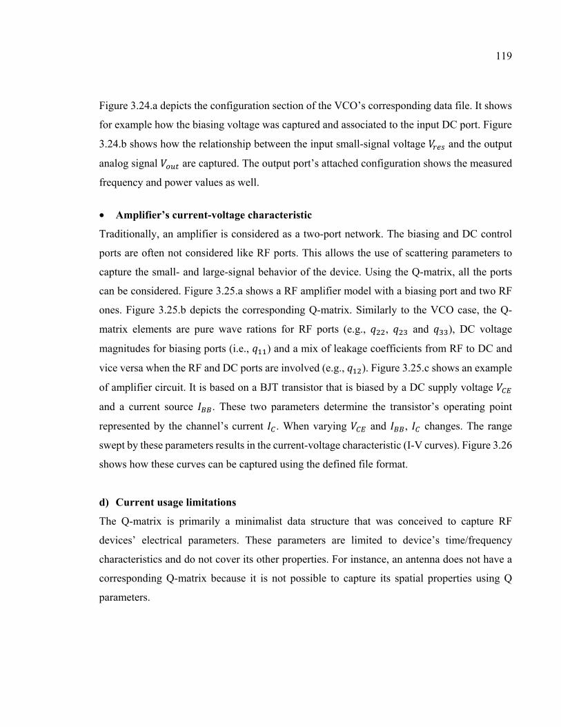
119
Figure 3.24.a depicts the configuration section of the VCO’s corresponding data file. It shows
for example how the biasing voltage was captured and associated to the input DC port. Figure
3.24.b shows how the relationship between the input small-signal voltage and the output
analog signal are captured. The output port’s attached configuration shows the measured
frequency and power values as well.
• Amplifier’s current-voltage characteristic
Traditionally, an amplifier is considered as a two-port network. The biasing and DC control
ports are often not considered like RF ports. This allows the use of scattering parameters to
capture the small- and large-signal behavior of the device. Using the Q-matrix, all the ports
can be considered. Figure 3.25.a shows a RF amplifier model with a biasing port and two RF
ones. Figure 3.25.b depicts the corresponding Q-matrix. Similarly to the VCO case, the Q-
matrix elements are pure wave rations for RF ports (e.g., , and ), DC voltage
magnitudes for biasing ports (i.e., ) and a mix of leakage coefficients from RF to DC and
vice versa when the RF and DC ports are involved (e.g., ). Figure 3.25.c shows an example
of amplifier circuit. It is based on a BJT transistor that is biased by a DC supply voltage
and a current source . These two parameters determine the transistor’s operating point
represented by the channel’s current . When varying and , changes. The range
swept by these parameters results in the current-voltage characteristic (I-V curves). Figure 3.26
shows how these curves can be captured using the defined file format.
d) Current usage limitations
The Q-matrix is primarily a minimalist data structure that was conceived to capture RF
devices’ electrical parameters. These parameters are limited to device’s time/frequency
characteristics and do not cover its other properties. For instance, an antenna does not have a
corresponding Q-matrix because it is not possible to capture its spatial properties using Q
parameters.
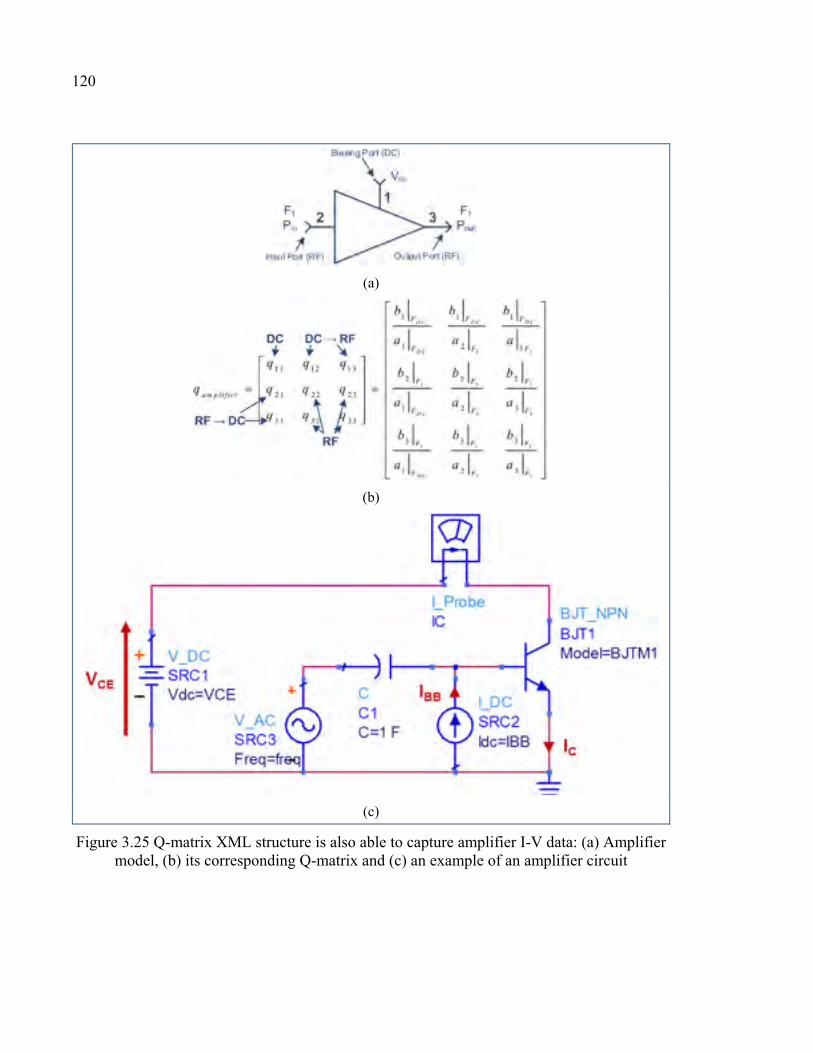
120
(a)
(b)
(c)
Figure 3.25 Q-matrix XML structure is also able to capture amplifier I-V data: (a) Amplifier model, (b) its corresponding Q-matrix and (c) an example of an amplifier circuit
121
Figure 3.26 Q-matrix XML structure is also able to capture amplifier I-V data: The data file corresponding to the amplifier model of Figure 3.25
This said, various challenges should be addressed in order to make the Q-matrix effective and
useful. The first is the need to develop tools that implement the corresponding formalism. The
second is a wide adoption by the current RF commercial design frameworks and instruments.
The adoption of the Q-matrix remains limited because most design frameworks and
measurement instruments carry out linear and nonlinear simulations and tests separately. Then,
it becomes difficult to consider Q-matrix elements in a mix of DC and RF ports at the same
time. This is in fact a limitation of the current Q-matrix paradigm. To resolve this issue, the Q-
matrix mathematical formalism should be extended further to derive useful relationships that
can be easily and directly used to calculate the Q-matrix elements. Such formalism will be
similar to those used in the derivation of the traditional scattering parameters as well as the
122
newly-introduced X parameters54 (i.e., nonlinear scattering parameters) which gave birth not
only to numerous EDA tools but also to measurement instruments (e.g., Vector Network
Analyzer for S parameters and Power Network Analyzer X for X parameters). The derivation
of an extended and complete Q-matrix mathematical formalism that could enable its immediate
adoption by the industry requires an effort that falls beyond the scope of this thesis. It is an
outstanding future work.
3.3.6 Summary View of the Proposed Design Flow
In order to address the various design challenges of paragraph 3.2, we have so far defined two
main elements:
− A five-step design flow: it consists of a succession of five design stages that start with
device’s functional description. This allows to capture device’s specifications using high-
level modeling languages such as SysML/UML and to exchange them using XML. Then,
this functional description can be validated in the analysis step where various system-level
analyses may take place in the purpose of identifying an initial design solution to begin
with. This design solution is used in the synthesis step for further optimization. Design
partitioning is leveraged using granularity refinement. Implementation technology and
physical details are considered using technology mapping. Once the final solution is
optimized, it then can be manufactured and tested;
− The Q-matrix: it is a minimalist data structure for device’s electrical properties that allows
to store, share and compare design data from the early design stages throughout the
device’s operation phase. For this purpose, it is associated to a XML-based file data format
that can embody any useful design, test or operation relevant information in addition to the
Q parameters.
54 X parameters denote a mathematical superset of S-parameters for nonlinear network analysis that is applicable for both small- and large-signal configurations. Verspecht, Jan. 2005. « Large-signal network analysis ». Microwave Magazine, IEEE, vol. 6, no 4, p. 82-92., Verspecht, Jan, et David E Root. 2006. « Polyharmonic distortion modeling ». Ibid., vol. 7, no 3, p. 44-57.
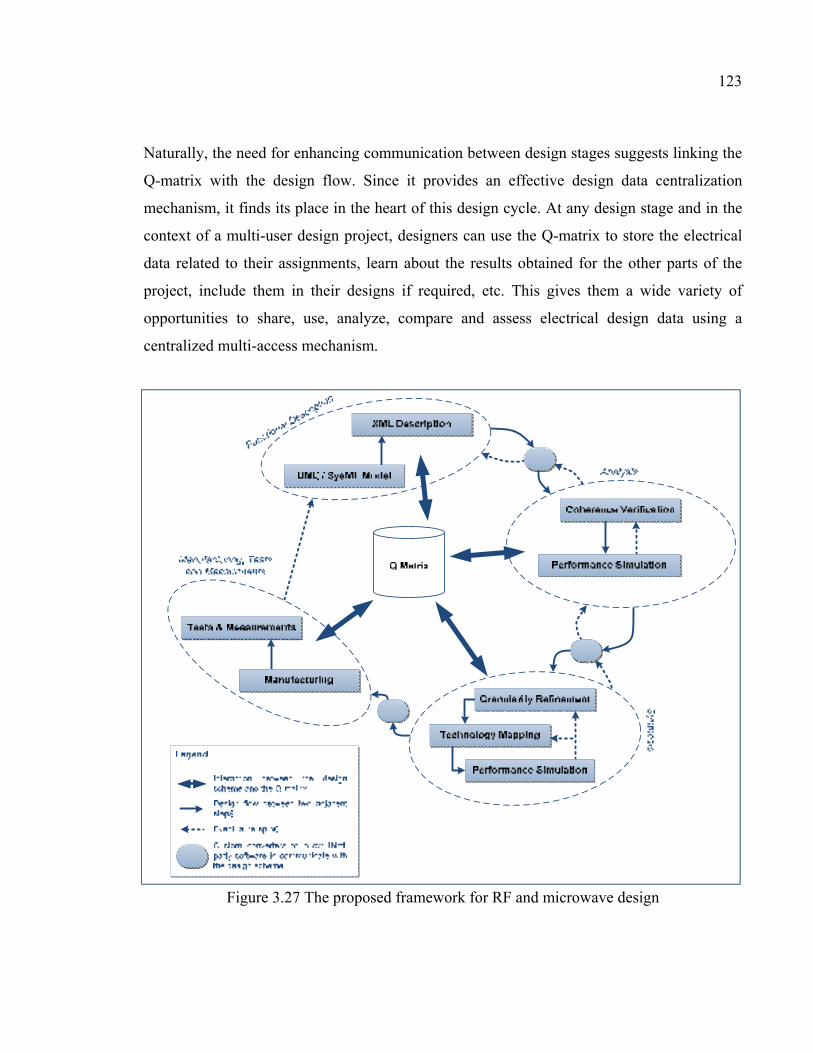
123
Naturally, the need for enhancing communication between design stages suggests linking the
Q-matrix with the design flow. Since it provides an effective design data centralization
mechanism, it finds its place in the heart of this design cycle. At any design stage and in the
context of a multi-user design project, designers can use the Q-matrix to store the electrical
data related to their assignments, learn about the results obtained for the other parts of the
project, include them in their designs if required, etc. This gives them a wide variety of
opportunities to share, use, analyze, compare and assess electrical design data using a
centralized multi-access mechanism.
Figure 3.27 The proposed framework for RF and microwave design
124
As shown in Figure 3.27, the marriage between the design flow and the Q-matrix establishes a
tool-neutral end-to-end design framework for RF devices. However, the fundamental changes
in design concepts that are proposed in this framework may be incompatible with the current
design tools and environments. For this reason, this framework has added specific converters
between the different design stages in order to accommodate the various EDA tools currently
in use. In fact, these converters allow the support of various data file formats and
communication channels (e.g., co-simulation pipes) in order to reduce the incompatibility
influence and allow the adoption of a wide range of existent simulation and design tools.
3.4 Mapping Framework Provisions to Designated Design Challenges
The design framework was first proposed to address the design challenges enumerated in Table
3.1. As detailed in Table 3.7, the various mechanisms adopted in this framework are expected
to bring contributions at different levels:
− Design flow: it was conceived to link the different design stages and streamline the design
effort. Separate design stages and steps allow effective design partitioning and improve
significantly collaboration between designers (A, P3) as well as enhancing design
concurrency (A, P4). Given relevant design tools, the design flow allows effective design
exchange (A, P2), reuse (A, P6) and technology insertion (A, P7) because design models,
data and technology information can be provided at the appropriate design step and for the
suitable design purpose;
− Functional Description: it is among the major contributions of the proposed design
framework. By focusing on high-level modeling and XML storage, collaboration (B, P3),
exchange (B, P2) and design reuse (B, P6) become easier because models are expected to
be comprehensive and amenable for automation. Being model-centered, functional
description brings a higher level of abstraction which allows the use of automated
verification approaches for better design consistency (B, P5). However, this step does not
influence technology insertion (B, P7) because it is not expected to deal with;
− Analysis: this step significantly enhances design consistency (C, P5). Using the models
resulting from the functional description, it uses an approach of coherence verification and
125
system-level analysis in order to check if these models are consistent. The use of models
and relevant tools at this step allows also for better automation (C, P1);
− Synthesis: it is a concept that was conceived to address two main issues: automation and
technology insertion. At this regard, this step embodies two mechanisms for enhancing
automation. First, granularity refinement allows the search of the best design solution.
Then, automated (or/semi-automated) design-to-manufacture procedures and tools are
used for the implementation of this solution. Technology mapping is an intermediate step
that is expected to include the relevant technology information;
− Q-matrix: if design information are provided and exchanged using models, design data are
centralized using the Q-matrix. This centralization provides simultaneous access for
various designers and tools which enhances design concurrency and collaboration. The
storage of multi-source and multi-purpose design data contributes to better design
consistency. The XML data structure and metadata provides practical tools for data
exchange and reuse. Tools interacts better through the Q-matrix. In addition, the interaction
with the Q-matrix is tool-based which improves design automation.
The proposed design framework has brought new concepts in addressing major RF design
issues. If analysis (including coherence verification and system-level analysis) and synthesis
(including granularity refinement and technology mapping) are amenable for automation due
to the algorithms and tools that can be developed to handle the design, these mechanisms use
a basic ingredient: models that are developed during the functional description step. The
absence of comprehensive and usable models compromises these steps. By opposition to other
domains (i.e., digital design, software development, etc.) where the use of models is a habit,
high-level modeling is not common in RF design. For this purpose, two issues should be
resolved at this regard: effective models development and use. In addition, modeling activity
should guarantee design independence from technology (particularly at higher levels of
design). At this regard, we propose to deepen our research in hardware abstraction for
augmenting the current framework (especially functional description) with mechanisms and
concepts that contribute to resolve these issues.
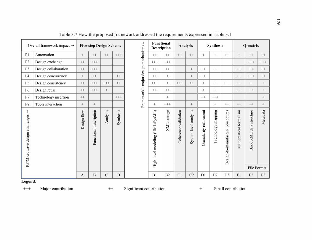
Table 3.7 How the proposed framework addressed the requirements expressed in Table 3.1
Overall framework impact Five-step Design Scheme
Fra
mew
ork’
s m
ajor
des
ign
mec
hani
sms Functional
Description Analysis Synthesis Q-matrix
P1 Automation + ++ ++ +++ ++ ++ ++ ++ + + ++ + ++ ++
P2 Design exchange ++ +++ +++ +++ +++ +++
P3 Design collaboration ++ +++ ++ ++ + ++ + ++ ++ ++
P4 Design concurrency + ++ ++ ++ + + ++ ++ +++ ++
P5 Design consistency ++ +++ +++ ++ +++ + +++ ++ + + +++ ++ + +
P6 Design reuse ++ +++ + ++ ++ + + ++ ++ +
P7 Technology insertion ++ +++ + ++ +++ +
P8 Tools interaction + + + +++ + + ++ ++ ++ +
RF
/Mic
row
ave
desi
gn c
halle
nges
Des
ign
flow
Fun
ctio
nal d
escr
iptio
n
Ana
lysi
s
Syn
thes
is
Hig
h-le
vel m
odel
ing
(UM
L/S
ysM
L)
XM
L s
tora
ge
Coh
eren
ce v
alid
atio
n
Sys
tem
-lev
el a
naly
sis
Gra
nula
rity
ref
inem
ent
Tec
hnol
ogy
map
ping
Des
ign-
to-m
anuf
actu
re p
roce
dure
s
Mat
hem
atic
al f
orm
alis
m
Bas
ic X
ML
dat
a st
ruct
ure
Met
adat
a
File Format
A B C D B1 B2 C1 C2 D1 D2 D3 E1 E2 E3
Legend:
+++ Major contribution ++ Significant contribution + Small contribution
126
127
3.5 Conclusion
In this chapter, we presented a five-step design scheme that redefines the main steps required
for RF front-ends’ design. The first step, namely “Functional Description”, aims to uncouple
the RF functionality from physical-level details. To do so, it captures the specifications using
expressive modeling languages (e.g., SysML). The next step, namely “Analysis”, allows
validating the developed models using a mechanism of coherence verification. If the models
are error-free, various system-level analyses may take place to figure out a suitable initial
design solution that meets the specifications. This initial solution is used in the third design
step, namely “Synthesis”, to implement the final solution. This takes place through three sub-
steps: The first optimizes the design solution by iterative granularity refinement. The second
includes physical considerations in the design. Then, the resulting design is optimized and
validated through performance simulations. The step of “Synthesis” is meant to provide a
ready-to-manufacture design solution to fabricated and tested in the following design steps
(i.e., manufacturing and test and measurements). It is aimed to make the design process as
much automated as possible. In the heart of the proposed design cycle, we defined a multi-
dimensional data structure, namely Q-matrix, which holds all the electrical design data. On the
contrary of existent data structures, the Q-matrix is not only accessible at all the design stages
but also accompanies the manufactured design during the operation phase.
Each stage of the proposed design framework includes mechanisms that address some of the
shortcomings and drawbacks encountered in today’s design practice. By making design model-
centric, this framework aims to raise the abstraction level, which allows better design space
exploration and higher automation. However, it poses two significant challenges to designers:
model development and usage. From practical point of view, designers should be able to
develop models at different levels of abstraction and easily use them to derive design solutions.
To overcome this practical issue with the proposed design framework, a clear abstraction
strategy should be elaborated. Clear abstraction levels for RF circuits should be defined. For
each of them, specific models are also dedicated. The next chapter attempts to discuss and
resolve this issue.

CHAPTER 4
HARDWARE ABSTRACTION-BASED STRATEGY FOR RF AND MICROWAVE DESIGN
4.1 Introduction
In the previous chapter, we presented the foundations of a new design methodology for
RF/microwave devices. It consists of a five-step design scheme that starts with functional
description. This first stage uses high-level modeling languages to capture the intended
system’s specifications. The corresponding models are then validated in the following step,
namely analysis, which ensures the coherence of the captured specifications and enables the
identification of an initial design solution, ideally in a technology-independent manner. This
solution is then refined and optimized in the following design stage, namely synthesis, to
develop a ready-to-manufacture solution. Various considerations are introduced in this step.
For instance, technology details are included via technology mapping. Accordingly, the final
layout is produced and verified. Once ready, manufacturing and test tasks can take place. All
these design steps are built around the Q-matrix, a centralized tool-neutral data structure that
captures the design electrical data throughout all design stages. Added to functional
description, the modular Q-matrix enables better design productivity through enhancing design
collaboration, concurrency and empowering tools interaction.
As previously mentioned, the proposed design methodology introduced several mechanisms
in order to alleviate the main challenges facing modern RF design. In particular, functional
description allows for a higher-level of abstraction, which contributes to productivity
enhancement and automation improvement. Despite the fact that using high-level modeling for
functional description enables the access to higher levels of abstraction, the development and
mainly the use of the corresponding models impose significant challenges. First, clear
abstraction levels are needed in order to unify the view of RF devices. Then, moving from an
abstraction level to another requires formal mechanisms. Finally, the interference of
technology considerations within each design stage should be better controlled in order to
130
avoid premature design loops and maintain an efficient design space exploration. To do so, we
propose in this chapter to investigate further the existing strategies of hardware abstraction in
the aim of elaborating a coherent abstraction strategy to streamline with the proposed design
framework. In the first section of this chapter, we review the abstraction concepts in different
engineering domains ranging from digital and mixed-signal design to other engineering
domains such as software development. In the light of this review, we propose in the second
section a hardware abstraction strategy for RF design. Then, we propose the “SysML profile
for RF devices” which provides a modeling template in accordance to the abstraction strategy
in order to help designers developing functional descriptions for RF devices and systems.
Finally, we streamline the abstraction strategy with the design scheme of chapter 3 within a
complete design framework.
4.2 Hardware Abstraction in Various Domains
Hardware abstraction is a concept that has proven its usefulness in various engineering
domains. In this first section, we present this concept in some detail. Then, we review the
hardware abstraction strategy in use in domains close to RF design, namely digital and mixed-
signal design. We extend this review to include other successful experiences such as hardware
abstraction strategies used in computer engineering and software development.
4.2.1 Definition and Advantages
Abstraction is defined by Dictionary.com55 as “the act of considering something as a general
quality or characteristic, apart from concrete realities, specific objects, or actual instances”.
The psychologists Goldstone and Barsalou assert in (Goldstone et Barsalou, 1998) that “to
abstract is to distill the essence from its superficial trappings”. The sixth edition of Oxford
Dictionary of Computing56 defines abstraction as “the principle of ignoring those aspects of a
55 Dictionary.com (whose website is www.dictionary.com) is a company that presents itself as a provider of online “reliable access to millions of English definitions, synonyms, audio pronunciations, example sentences, translations and spelling help through [its] services”.
56 The Oxford Dictionary of Computing is a computer science dictionary that is published by the Oxford University Press.
131
subject that are not relevant to the current purpose in order to concentrate more fully on those
that are” (Rozenberg et Vaandrager, 1998). Therefore, all these definitions suggest that
abstraction is the act of uncoupling the fundamental characteristics of an object from the details
of its construction. Thus, its main purpose is presenting a simplified view of a complex reality
by hiding its unnecessary attributes and aspects. This is why abstractions can be of various
types due to real world complexity. For example, an abstraction may be mathematical in a way
that only the equations describing the fundamental characteristics of an object are considered.
It can also be physical that the fundamental nature of that object is considered without any
other specific attributes (Saitta et Zucker, 2013). In a myriad of disciplines (e.g., art, cognition,
vision, etc.), abstraction is often informal because it uses “lossy” mechanisms (e.g.,
generalization, approximation, etc.) in order to hide irrelevant aspects of a real-world object.
The resulting object’s representation is often deprived of useful information. However,
rigorous domains, particularly related to engineering (e.g., computer science, artificial
intelligence, digital design, etc.) use formal models to make abstraction of objects, systems and
programs (Saitta et Zucker, 2013). Modeling introduces the concept of abstraction level that
allows recovering the discarded information when required. In this regard, an appropriate
model for abstraction should satisfy at least two properties (Saitta et Zucker, 2013):
1. Reasonability: the conceptualization must produce results understandable by and close to
those produced by human reasoning, and
2. Automation and usability: the model can be derived into appropriate implementations using
suitable tools.
As explicitly presented in (Saitta et Zucker, 2013), the major benefits of abstraction can be
summarized as following:
− Simplicity: abstraction reduces complexity by producing an object view as simple as
possible;
− Relevance and information control: abstraction is meant to capture only the relevant
aspects of an object. This includes the control of the information amount needed to describe
that object at a given level of abstraction;
132
− Granularity: an object can be described at different levels of detail. Consequently,
capturing fewer details results in more abstract representations and vice-versa;
− Uncoupling abstract from concrete views: object abstraction provides a distance with its
concrete status. The most the concrete status is hidden, the highest the abstraction level is;
− Naming: at a given abstraction level, the object name becomes the synonym of the object
properties and attributes accessible at that level of abstraction. This strong semantics allow
easier understandability of a complex system;
− Reformulation: an abstraction is not unique which makes it easy to reformulate the same
object properties in different formal ways that can be suitable for different scenarios.
In summary, the major benefit of abstraction remains its ability to manage complexity and
simplify complicated systems. For this reason, some computer architects consider that
“abstraction is probably the most powerful tool available to managing complexity” (Archer,
Head et Yuan, 1996). This said, most engineering literature uses frequently the term
“Hardware Abstraction Layer” (HAL) rather than “Abstraction” and “Hardware Abstraction”
(e.g., sensor networks (Handziski et al., 2005), System-on-Chip (Yoo et Jerraya, 2003), etc.)
to refer to the adopted abstraction strategies. This is typically related to the layered nature of
the systems using this HALs. For instance, HAL is well known and predominant in computer
systems because it serves as a logical division that makes the link between software and
hardware layers.
As far as the RF design is concerned, we define “Hardware Abstraction” in this thesis as “the
concept of masking physical details of hardware, allowing the designer to focus on the RF
functionality rather than the details of its implementation”. Thus, it is a way to describe the
functionality without considering the physical implementation details of a communication
system. We also use the term “Hardware Abstraction” instead of “Abstraction” to express the
predominant technology-dependent aspects of RF design.
133
4.2.2 Hardware Abstraction in Digital and Mixed-Signal Design
As mentioned in chapter 1, adding more functionality while reducing chip area and power
consumption leads to growing complexity. Managing that complexity is a major challenge in
both digital and mixed-signal design. For decades, digital designers have been successful in
alleviating their design’s complexity due to the hierarchical design approach they adopted for
this purpose (Gerez, 1999; Rabaey, Chandrakasan et Nikolic, 2002; Rubin, 1987). That design
approach consists of partitioning a complex system into several subparts which are arranged
in a given hierarchy. Each level of this hierarchy is arranged in a way that it fully characterizes
a given perspective of the design. The details of the lower levels are not needed to functionally
describe that perspective. At this regard, hardware abstraction has played an important role for
two main reasons. First, it enabled a coherent mechanism to hide the underlying details without
losing them. In fact, the characteristics of each component (e.g., structure and behavior) are
captured by a black-box view (i.e., commonly called model). The model represents a given
functionality and presents all the information required to deal with the component at the next
level of hierarchy (Rabaey, Chandrakasan et Nikolic, 2002). Second, it enabled an effective
divide-and-conquer process that carefully beaks up the design into smaller pieces making them
easier to implement and verify. Each piece corresponds to a model that abstracts the lower
levels by creating a new representation of them. This representation is able to fully describe
the characteristics of the underlying structure without recalling its composition details (e.g.,
physical, circuit, logical, etc.). Accordingly, design complexity is then substantially reduced
(Rabaey, Chandrakasan et Nikolic, 2002).
a) Abstraction levels
To raise the abstraction level in digital design, a new representation (i.e., is associated) should
be created for each design viewpoint. In this regard, the nature of digital design (i.e., discrete
and linear) and the implementation technologies (i.e., silicon-based) were of great value to
designers. First, the physical properties of devices were captured by electrical circuits. Since
the digital signals are mainly discrete, these circuits were gathered to create logical gates that
can be fully characterized using Boolean equations. Then, these gates can be arranged to build
more complex logical functionalities (e.g., multiplexers, adders, multipliers, etc.). These
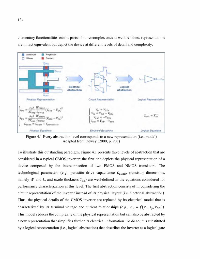
134
elementary functionalities can be parts of more complex ones as well. All these representations
are in fact equivalent but depict the device at different levels of detail and complexity.
Figure 4.1 Every abstraction level corresponds to a new representation (i.e., model) Adapted from Dewey (2000, p. 908)
To illustrate this outstanding paradigm, Figure 4.1 presents three levels of abstraction that are
considered in a typical CMOS inverter: the first one depicts the physical representation of a
device composed by the interconnection of two PMOS and NMOS transistors. The
technological parameters (e.g., parasitic drive capacitance , transistor dimensions,
namely and , and oxide thickness ) are well-defined in the equations considered for
performance characterization at this level. The first abstraction consists of in considering the
circuit representation of the inverter instead of its physical layout (i.e. electrical abstraction).
Thus, the physical details of the CMOS inverter are replaced by its electrical model that is
characterized by its terminal voltage and current relationships (e.g., = , , ).
This model reduces the complexity of the physical representation but can also be abstracted by
a new representation that simplifies further its electrical information. To do so, it is substituted
by a logical representation (i.e., logical abstraction) that describes the inverter as a logical gate
135
(i.e., in this case a NOT gate). This logical model can be formally characterized using Boolean
algebra equations and the related characterizations such as truth tables (Dewey, 2000).
In practice, this paradigm gave birth to five57 distinct levels of abstraction which are commonly
defined as following (see Figure 4.2) (Rabaey, Chandrakasan et Nikolic, 2002):
1. Device: it is the lowest level of abstraction. It gathers the physical components that cannot
be conceptually broken further. They are generally considered as the leaves of the design
hierarchy. Among the components defined at this level, we count transistors, capacitors
and resistors;
2. Circuit: it is the level where devices are assembled in and represented by a block based on
their electrical characteristics (e.g., voltage, current). The corresponding abstraction is
electrical;
3. Gate: this level abstracts circuits into logical elements that can be defined by Boolean
algebra equations and related truth tables. The logical abstraction veils all the underlying
physical and electrical information. Signals at this level are no longer continuous. The
interaction with the gate is made via discrete-time signals following a given rhythm (i.e.,
generally controlled by a reference clock) through designated input and output ports;
4. Module: a module is a collection of gates implementing a given functionality (e.g., add,
multiply, select, etc.). The corresponding abstraction is functional;
5. System: a system is a collection of modules that should meet given specifications. It is
commonly considered as the highest abstraction level since a system can be defined as a
“system of systems”. Designers focus mostly on the system’s architecture. The
architectural view describes how the underlying modules are interconnected, configured
and should interact. High-level algorithms, modeling languages and paradigms are
frequently used to describe the system’s architecture (e.g., VHDL, Verilog, Petri nets).
57 In some references (e.g., Xiu, Liming. 2007. VLSI circuit design methodology demystified: a conceptual taxonomy. John Wiley & Sons.), only four abstraction levels are considered. The circuit and gate levels are considered as a unique abstraction level that is referred to as “cell level”.
136
In fact, abstraction levels are practically useful when considered in the context of a design
flow. The abstraction levels of Figure 4.2 result into three distinct design domains (see Figure
4.3) (Gerez, 1999):
1. The behavioral domain: in this domain, the design relies on behavioral models. A
behavioral model is a black-box view of the part (or collection of parts) under design. It
does not make any reference to technology nor needs any physical details as prerequisite
to work. This type of models is based on mathematical formalisms, algorithms and/or
sequential interaction diagrams (e.g., state machines) in order to define how the modeled
part or system works. Its structure defines a set of input and output parameters. The input
parameters can be used to provide data (e.g., stimulus, measurements, etc.) to the model
and the output parameters make it possible to evaluate the model’s response. The accuracy
of the model depends on its formal definition and the quality of data that is provided (Arabi
et Ali, 2008; Gerez, 1999). Behavioral modeling can be typically used at all abstraction
levels. At the physical level, a device can be described by its intrinsic physical parameters.
For example, a transistor can be defined by the relationship between its channel current
and its gate, drain and source voltages. At circuit level, the relationships between the
various voltages and currents can define how a given circuit works. At a logical level,
Boolean algebra equations are enough to describe how gates and logic units operate. At
higher abstraction levels, algorithms and paradigms can describe the behavior of a system
or a collection of subsystems (Gerez, 1999);
2. The structural domain: what matters the most in this domain is the system’s (or
subsystem’s, device’s) structure. It is almost exclusively interested in the description of the
subsystems (or sub-circuits) composing the system and how they are interconnected
together. This structure is commonly represented by algorithms (e.g., “ENTITY” in VHDL
and “SC_MODULE” in SystemC) at the higher abstraction levels (i.e., functional and
architectural) or captured in a graphical schematic at the other levels. Generally, a circuit
can have one or more behavioral descriptions associated to its structure representation
(Gerez, 1999);
3. The physical domain: it is also called the layout domain. Since the final output should be a
physical implementation of the system, this domain is interested on how the parts and
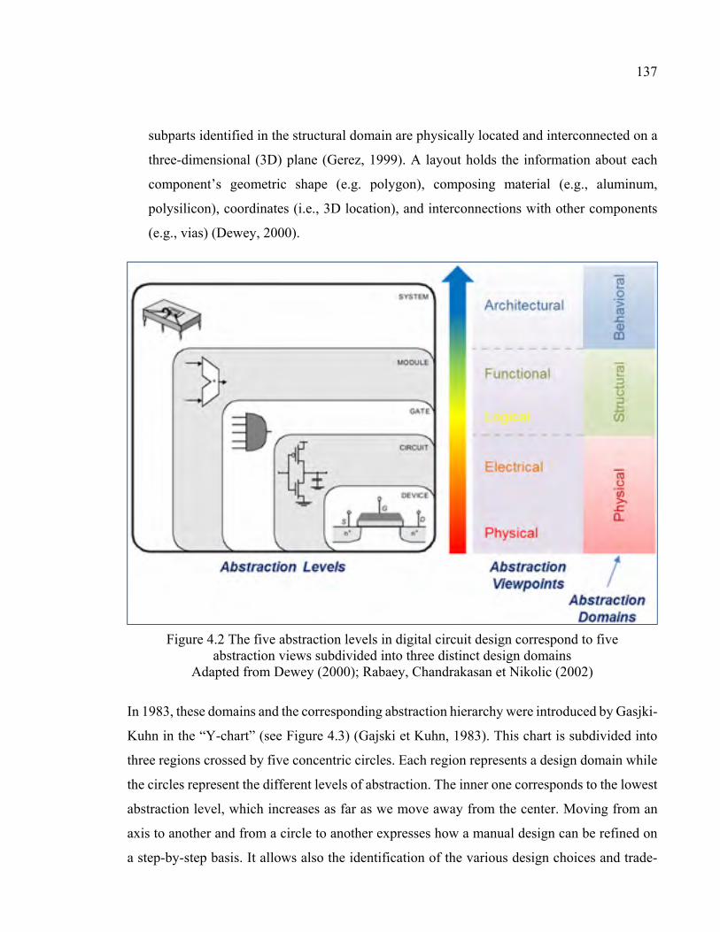
137
subparts identified in the structural domain are physically located and interconnected on a
three-dimensional (3D) plane (Gerez, 1999). A layout holds the information about each
component’s geometric shape (e.g. polygon), composing material (e.g., aluminum,
polysilicon), coordinates (i.e., 3D location), and interconnections with other components
(e.g., vias) (Dewey, 2000).
Figure 4.2 The five abstraction levels in digital circuit design correspond to five abstraction views subdivided into three distinct design domains
Adapted from Dewey (2000); Rabaey, Chandrakasan et Nikolic (2002)
In 1983, these domains and the corresponding abstraction hierarchy were introduced by Gasjki-
Kuhn in the “Y-chart” (see Figure 4.3) (Gajski et Kuhn, 1983). This chart is subdivided into
three regions crossed by five concentric circles. Each region represents a design domain while
the circles represent the different levels of abstraction. The inner one corresponds to the lowest
abstraction level, which increases as far as we move away from the center. Moving from an
axis to another and from a circle to another expresses how a manual design can be refined on
a step-by-step basis. It allows also the identification of the various design choices and trade-
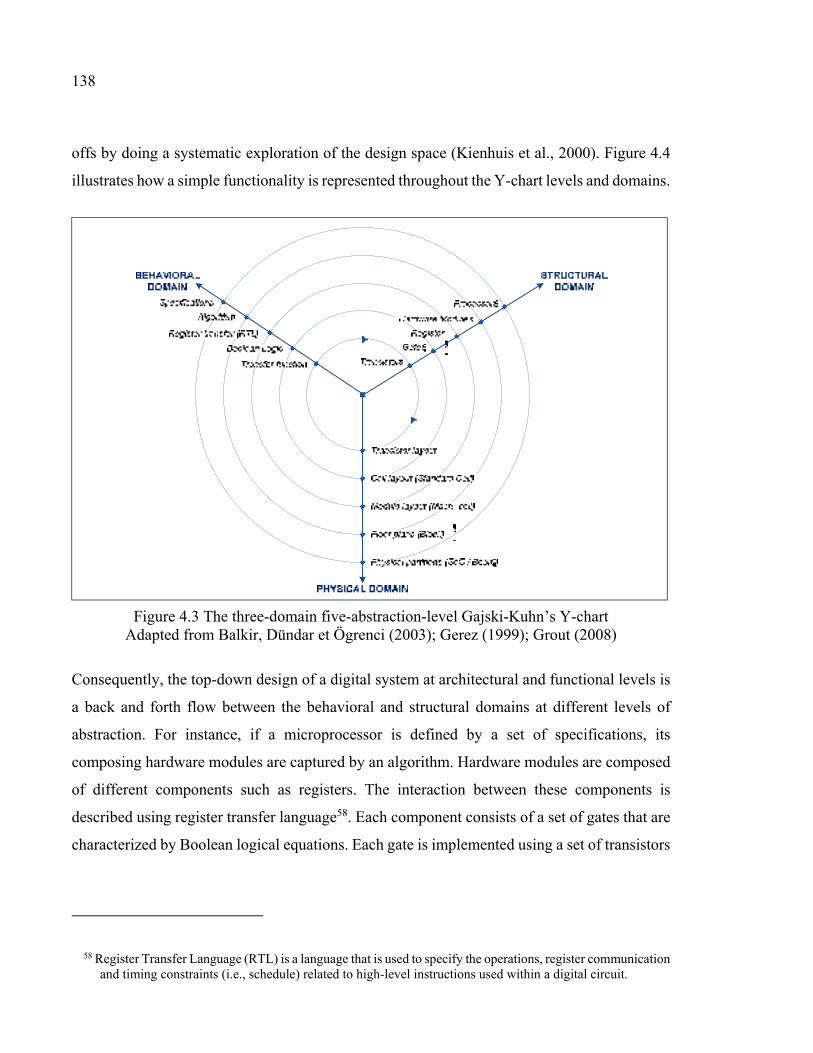
138
offs by doing a systematic exploration of the design space (Kienhuis et al., 2000). Figure 4.4
illustrates how a simple functionality is represented throughout the Y-chart levels and domains.
Figure 4.3 The three-domain five-abstraction-level Gajski-Kuhn’s Y-chart Adapted from Balkir, Dündar et Ögrenci (2003); Gerez (1999); Grout (2008)
Consequently, the top-down design of a digital system at architectural and functional levels is
a back and forth flow between the behavioral and structural domains at different levels of
abstraction. For instance, if a microprocessor is defined by a set of specifications, its
composing hardware modules are captured by an algorithm. Hardware modules are composed
of different components such as registers. The interaction between these components is
described using register transfer language58. Each component consists of a set of gates that are
characterized by Boolean logical equations. Each gate is implemented using a set of transistors
58 Register Transfer Language (RTL) is a language that is used to specify the operations, register communication and timing constraints (i.e., schedule) related to high-level instructions used within a digital circuit.
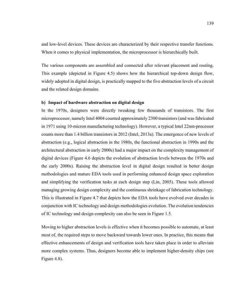
139
and low-level devices. These devices are characterized by their respective transfer functions.
When it comes to physical implementation, the microprocessor is hierarchically built.
The various components are assembled and connected after relevant placement and routing.
This example (depicted in Figure 4.5) shows how the hierarchical top-down design flow,
widely adopted in digital design, is practically mapped to the five abstraction levels of a circuit
and the related design domains.
b) Impact of hardware abstraction on digital design
In the 1970s, designers were directly tweaking few thousands of transistors. The first
microprocessor, namely Intel 4004 counted approximately 2300 transistors (and was fabricated
in 1971 using 10-micron manufacturing technology). However, a typical Intel 22nm-processor
counts more than 1.4 billion transistors in 2012 (Intel, 2013a). The emergence of new levels of
abstraction (e.g., logical abstraction in the 1980s, the functional abstraction in 1990s and the
architectural abstraction in early 2000s) had a major impact on the complexity management of
digital devices (Figure 4.6 depicts the evolution of abstraction levels between the 1970s and
the early 2000s). Raising the abstraction level in digital design resulted in better design
methodologies and mature EDA tools used in performing enhanced design space exploration
and simplifying the verification tasks at each design step (Lin, 2005). These tools allowed
managing growing design complexity and the continuous shrinkage of fabrication technology.
This is illustrated in Figure 4.7 that depicts how the EDA tools have evolved over decades in
conjunction with IC technology and design methodologies evolution. The evolution tendencies
of IC technology and design complexity can also be seen in Figure 1.5.
Moving to higher abstraction levels is effective when it becomes possible to automate, at least
most of, the required steps to move backward towards lower ones. In practice, this means that
effective enhancements of design and verification tools have taken place in order to alleviate
more complex systems. Thus, designers become able to implement higher-density chips (see
Figure 4.8).
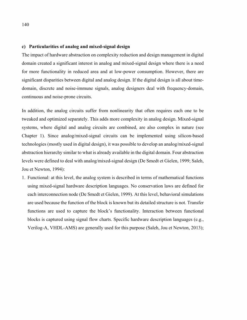
140
c) Particularities of analog and mixed-signal design
The impact of hardware abstraction on complexity reduction and design management in digital
domain created a significant interest in analog and mixed-signal design where there is a need
for more functionality in reduced area and at low-power consumption. However, there are
significant disparities between digital and analog design. If the digital design is all about time-
domain, discrete and noise-immune signals, analog designers deal with frequency-domain,
continuous and noise-prone circuits.
In addition, the analog circuits suffer from nonlinearity that often requires each one to be
tweaked and optimized separately. This adds more complexity in analog design. Mixed-signal
systems, where digital and analog circuits are combined, are also complex in nature (see
Chapter 1). Since analog/mixed-signal circuits can be implemented using silicon-based
technologies (mostly used in digital design), it was possible to develop an analog/mixed-signal
abstraction hierarchy similar to what is already available in the digital domain. Four abstraction
levels were defined to deal with analog/mixed-signal design (De Smedt et Gielen, 1999; Saleh,
Jou et Newton, 1994):
1. Functional: at this level, the analog system is described in terms of mathematical functions
using mixed-signal hardware description languages. No conservation laws are defined for
each interconnection node (De Smedt et Gielen, 1999). At this level, behavioral simulations
are used because the function of the block is known but its detailed structure is not. Transfer
functions are used to capture the block’s functionality. Interaction between functional
blocks is captured using signal flow charts. Specific hardware description languages (e.g.,
Verilog-A, VHDL-AMS) are generally used for this purpose (Saleh, Jou et Newton, 2013);
141
0 0 0 1 0 1
0 0 1 0 0 0
0 1 0 1 0 1
0 1 1 0 0 0
1 0 0 1 0 1
1 0 1 0 0 0
1 1 0 1 1 1
1 1 1 0 1 1
Figure 4.4 A digital functionality design changes its representation when it gradually goes through the behavioral, structural and physical domains
142
Figure 4.5 A top-down design flow mapped to the abstraction levels and design domains of Gajski-Kuhn’s Y-chart results in a back and forth top-down process
Taken from Gerez (1999, p. 7)
Figure 4.6 Raising the abstraction levels allowed more complex device models Taken from Sangiovanni-Vincentelli (2003, p. 67)
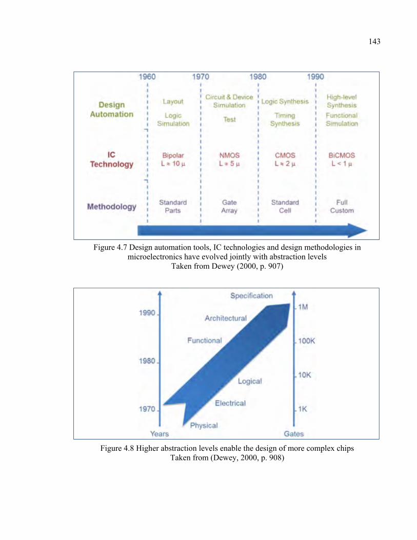
143
Figure 4.7 Design automation tools, IC technologies and design methodologies in microelectronics have evolved jointly with abstraction levels
Taken from Dewey (2000, p. 907)
Figure 4.8 Higher abstraction levels enable the design of more complex chips Taken from (Dewey, 2000, p. 908)
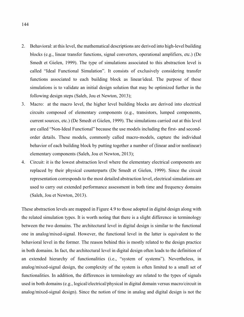
144
2. Behavioral: at this level, the mathematical descriptions are derived into high-level building
blocks (e.g., linear transfer functions, signal converters, operational amplifiers, etc.) (De
Smedt et Gielen, 1999). The type of simulations associated to this abstraction level is
called “Ideal Functional Simulation”. It consists of exclusively considering transfer
functions associated to each building block as linear/ideal. The purpose of these
simulations is to validate an initial design solution that may be optimized further in the
following design steps (Saleh, Jou et Newton, 2013);
3. Macro: at the macro level, the higher level building blocks are derived into electrical
circuits composed of elementary components (e.g., transistors, lumped components,
current sources, etc.) (De Smedt et Gielen, 1999). The simulations carried out at this level
are called “Non-Ideal Functional” because the use models including the first- and second-
order details. These models, commonly called macro-models, capture the individual
behavior of each building block by putting together a number of (linear and/or nonlinear)
elementary components (Saleh, Jou et Newton, 2013);
4. Circuit: it is the lowest abstraction level where the elementary electrical components are
replaced by their physical counterparts (De Smedt et Gielen, 1999). Since the circuit
representation corresponds to the most detailed abstraction level, electrical simulations are
used to carry out extended performance assessment in both time and frequency domains
(Saleh, Jou et Newton, 2013).
These abstraction levels are mapped in Figure 4.9 to those adopted in digital design along with
the related simulation types. It is worth noting that there is a slight difference in terminology
between the two domains. The architectural level in digital design is similar to the functional
one in analog/mixed-signal. However, the functional level in the latter is equivalent to the
behavioral level in the former. The reason behind this is mostly related to the design practice
in both domains. In fact, the architectural level in digital design often leads to the definition of
an extended hierarchy of functionalities (i.e., “system of systems”). Nevertheless, in
analog/mixed-signal design, the complexity of the system is often limited to a small set of
functionalities. In addition, the differences in terminology are related to the types of signals
used in both domains (e.g., logical/electrical/physical in digital domain versus macro/circuit in
analog/mixed-signal design). Since the notion of time in analog and digital design is not the
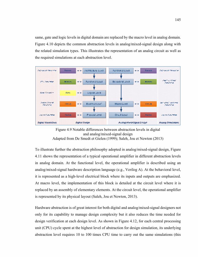
145
same, gate and logic levels in digital domain are replaced by the macro level in analog domain.
Figure 4.10 depicts the common abstraction levels in analog/mixed-signal design along with
the related simulation types. This illustrates the representation of an analog circuit as well as
the required simulations at each abstraction level.
Figure 4.9 Notable differences between abstraction levels in digital and analog/mixed-signal design
Adapted from De Smedt et Gielen (1999); Saleh, Jou et Newton (2013)
To illustrate further the abstraction philosophy adopted in analog/mixed-signal design, Figure
4.11 shows the representation of a typical operational amplifier in different abstraction levels
in analog domain. At the functional level, the operational amplifier is described using an
analog/mixed-signal hardware description language (e.g., Verilog A). At the behavioral level,
it is represented as a high-level electrical block where its inputs and outputs are emphasized.
At macro level, the implementation of this block is detailed at the circuit level where it is
replaced by an assembly of elementary elements. At the circuit level, the operational amplifier
is represented by its physical layout (Saleh, Jou et Newton, 2013).
Hardware abstraction is of great interest for both digital and analog/mixed-signal designers not
only for its capability to manage design complexity but it also reduces the time needed for
design verification at each design level. As shown in Figure 4.12, for each central processing
unit (CPU) cycle spent at the highest level of abstraction for design simulation, its underlying
abstraction level requires 10 to 100 times CPU time to carry out the same simulations (this
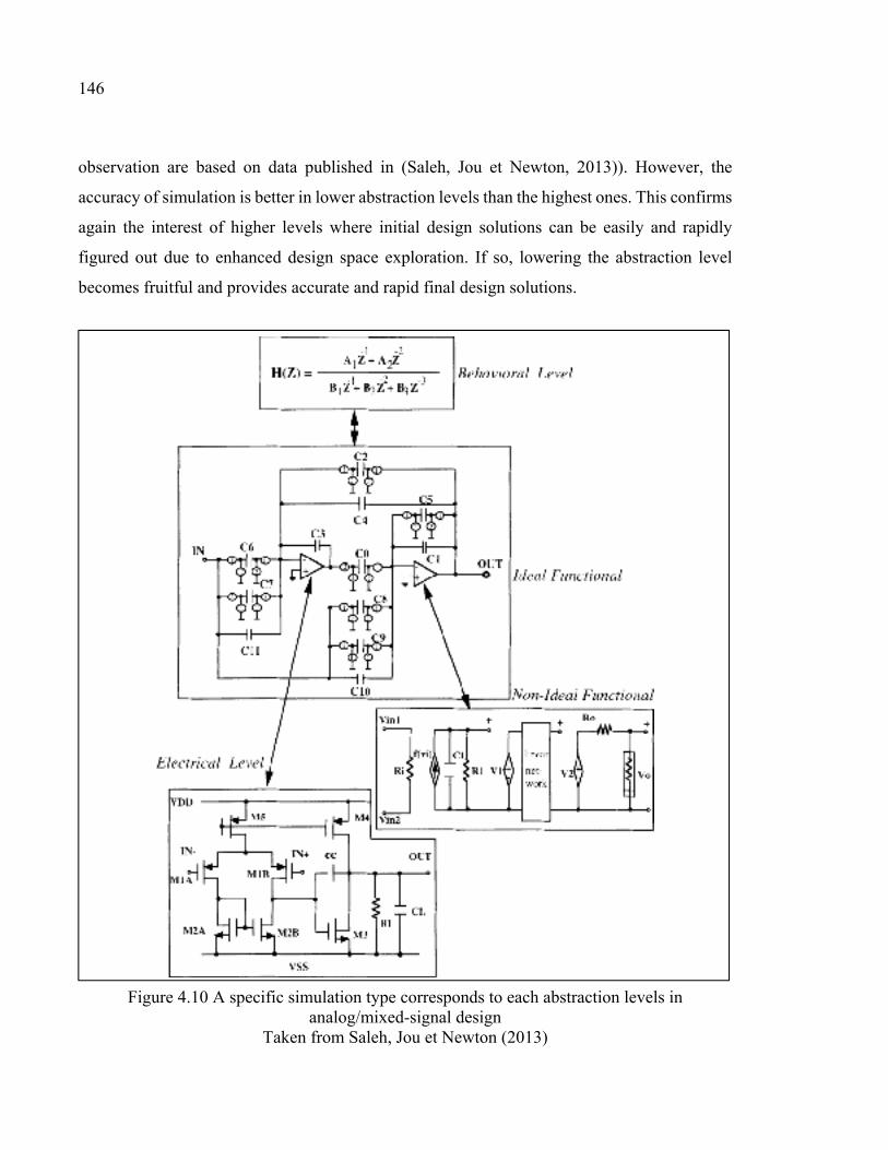
146
observation are based on data published in (Saleh, Jou et Newton, 2013)). However, the
accuracy of simulation is better in lower abstraction levels than the highest ones. This confirms
again the interest of higher levels where initial design solutions can be easily and rapidly
figured out due to enhanced design space exploration. If so, lowering the abstraction level
becomes fruitful and provides accurate and rapid final design solutions.
Figure 4.10 A specific simulation type corresponds to each abstraction levels in analog/mixed-signal design
Taken from Saleh, Jou et Newton (2013)
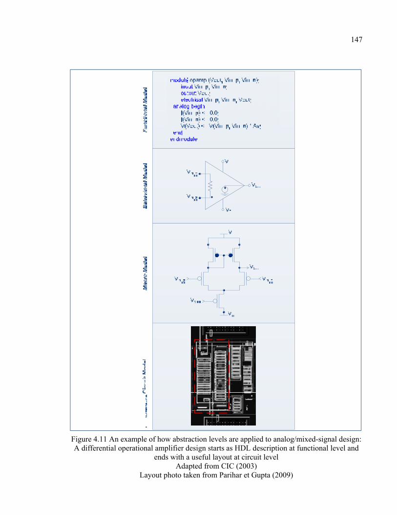
147
Figure 4.11 An example of how abstraction levels are applied to analog/mixed-signal design: A differential operational amplifier design starts as HDL description at functional level and
ends with a useful layout at circuit level Adapted from CIC (2003)
Layout photo taken from Parihar et Gupta (2009)
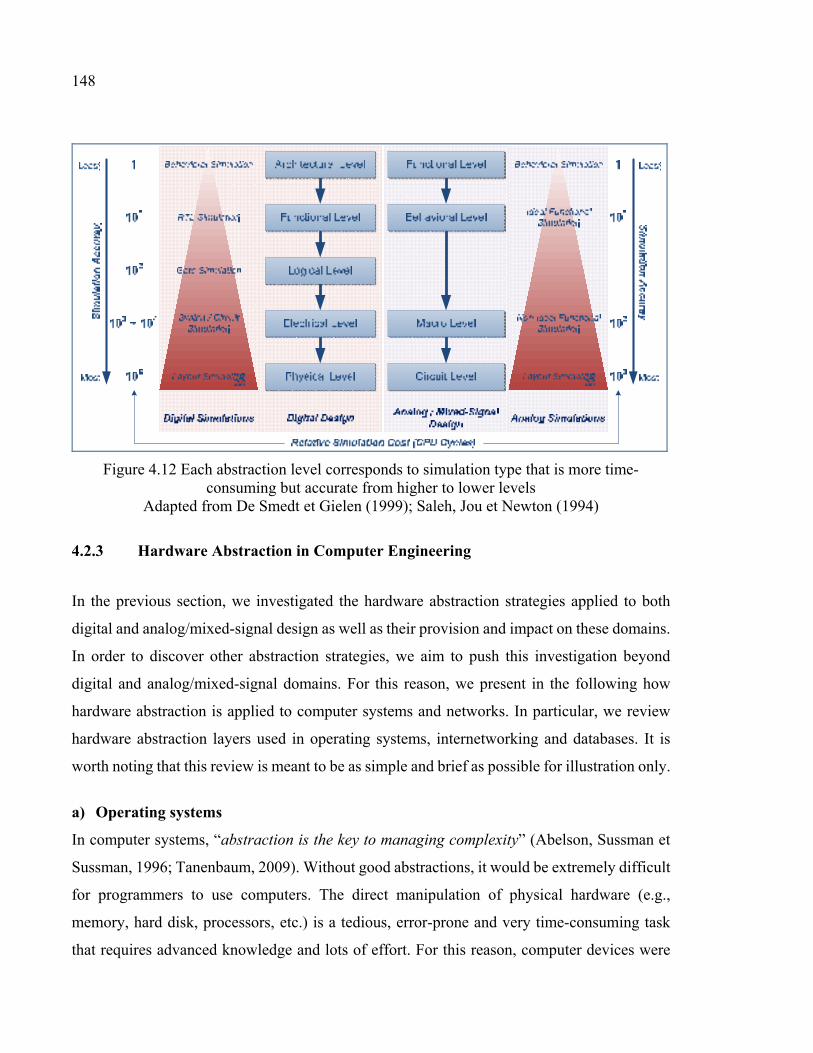
148
Figure 4.12 Each abstraction level corresponds to simulation type that is more time-consuming but accurate from higher to lower levels
Adapted from De Smedt et Gielen (1999); Saleh, Jou et Newton (1994)
4.2.3 Hardware Abstraction in Computer Engineering
In the previous section, we investigated the hardware abstraction strategies applied to both
digital and analog/mixed-signal design as well as their provision and impact on these domains.
In order to discover other abstraction strategies, we aim to push this investigation beyond
digital and analog/mixed-signal domains. For this reason, we present in the following how
hardware abstraction is applied to computer systems and networks. In particular, we review
hardware abstraction layers used in operating systems, internetworking and databases. It is
worth noting that this review is meant to be as simple and brief as possible for illustration only.
a) Operating systems
In computer systems, “abstraction is the key to managing complexity” (Abelson, Sussman et
Sussman, 1996; Tanenbaum, 2009). Without good abstractions, it would be extremely difficult
for programmers to use computers. The direct manipulation of physical hardware (e.g.,
memory, hard disk, processors, etc.) is a tedious, error-prone and very time-consuming task
that requires advanced knowledge and lots of effort. For this reason, computer devices were
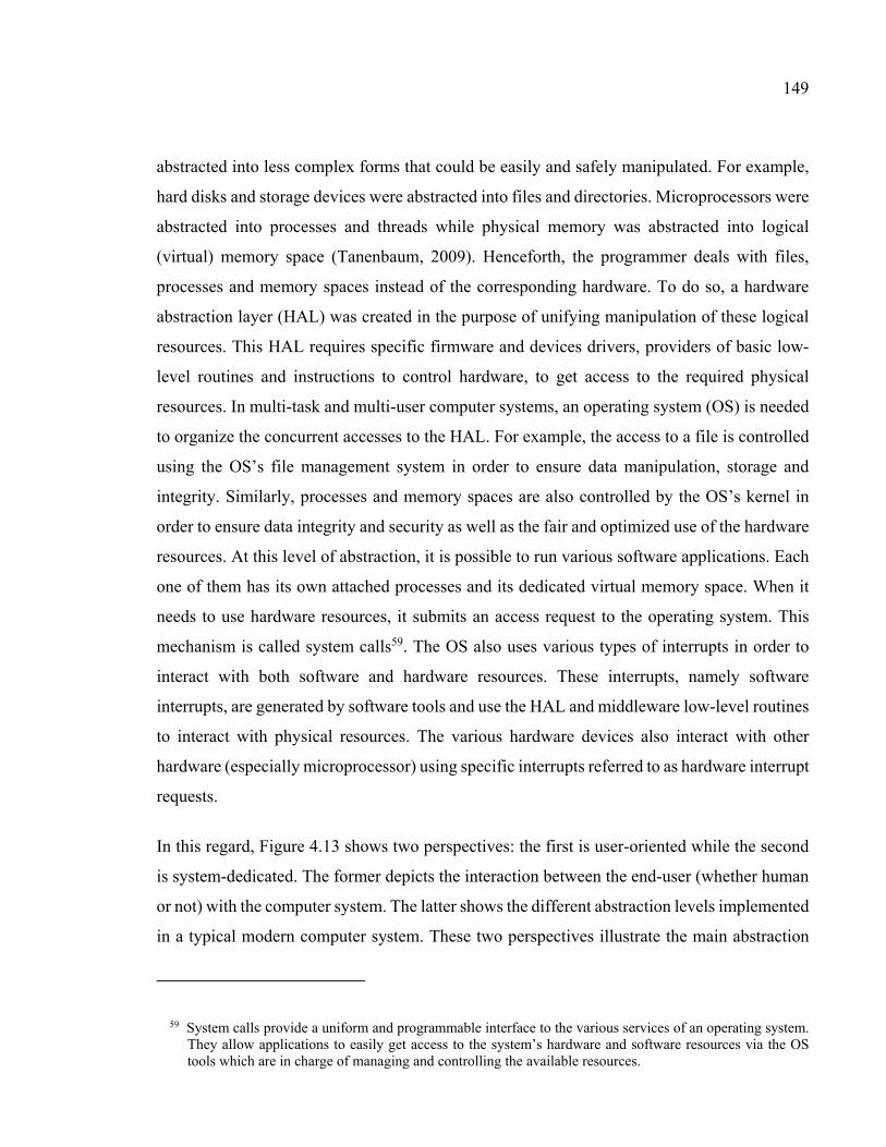
149
abstracted into less complex forms that could be easily and safely manipulated. For example,
hard disks and storage devices were abstracted into files and directories. Microprocessors were
abstracted into processes and threads while physical memory was abstracted into logical
(virtual) memory space (Tanenbaum, 2009). Henceforth, the programmer deals with files,
processes and memory spaces instead of the corresponding hardware. To do so, a hardware
abstraction layer (HAL) was created in the purpose of unifying manipulation of these logical
resources. This HAL requires specific firmware and devices drivers, providers of basic low-
level routines and instructions to control hardware, to get access to the required physical
resources. In multi-task and multi-user computer systems, an operating system (OS) is needed
to organize the concurrent accesses to the HAL. For example, the access to a file is controlled
using the OS’s file management system in order to ensure data manipulation, storage and
integrity. Similarly, processes and memory spaces are also controlled by the OS’s kernel in
order to ensure data integrity and security as well as the fair and optimized use of the hardware
resources. At this level of abstraction, it is possible to run various software applications. Each
one of them has its own attached processes and its dedicated virtual memory space. When it
needs to use hardware resources, it submits an access request to the operating system. This
mechanism is called system calls59. The OS also uses various types of interrupts in order to
interact with both software and hardware resources. These interrupts, namely software
interrupts, are generated by software tools and use the HAL and middleware low-level routines
to interact with physical resources. The various hardware devices also interact with other
hardware (especially microprocessor) using specific interrupts referred to as hardware interrupt
requests.
In this regard, Figure 4.13 shows two perspectives: the first is user-oriented while the second
is system-dedicated. The former depicts the interaction between the end-user (whether human
or not) with the computer system. The latter shows the different abstraction levels implemented
in a typical modern computer system. These two perspectives illustrate the main abstraction
59 System calls provide a uniform and programmable interface to the various services of an operating system. They allow applications to easily get access to the system’s hardware and software resources via the OS tools which are in charge of managing and controlling the available resources.
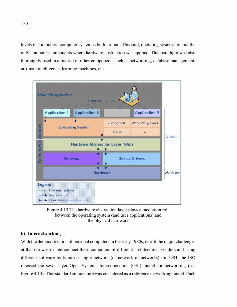
150
levels that a modern computer system is built around. This said, operating systems are not the
only computer components where hardware abstraction was applied. This paradigm was also
thoroughly used in a myriad of other components such as networking, database management,
artificial intelligence, learning machines, etc.
Figure 4.13 The hardware abstraction layer plays a mediation role between the operating system (and user applications) and
the physical hardware
b) Internetworking
With the democratization of personal computers in the early 1980s, one of the major challenges
at that era was to interconnect these computers of different architectures, vendors and using
different software tools into a single network (or network of networks). In 1984, the ISO
released the seven-layer Open Systems Interconnection (OSI) model for networking (see
Figure 4.14). This standard architecture was considered as a reference networking model. Each
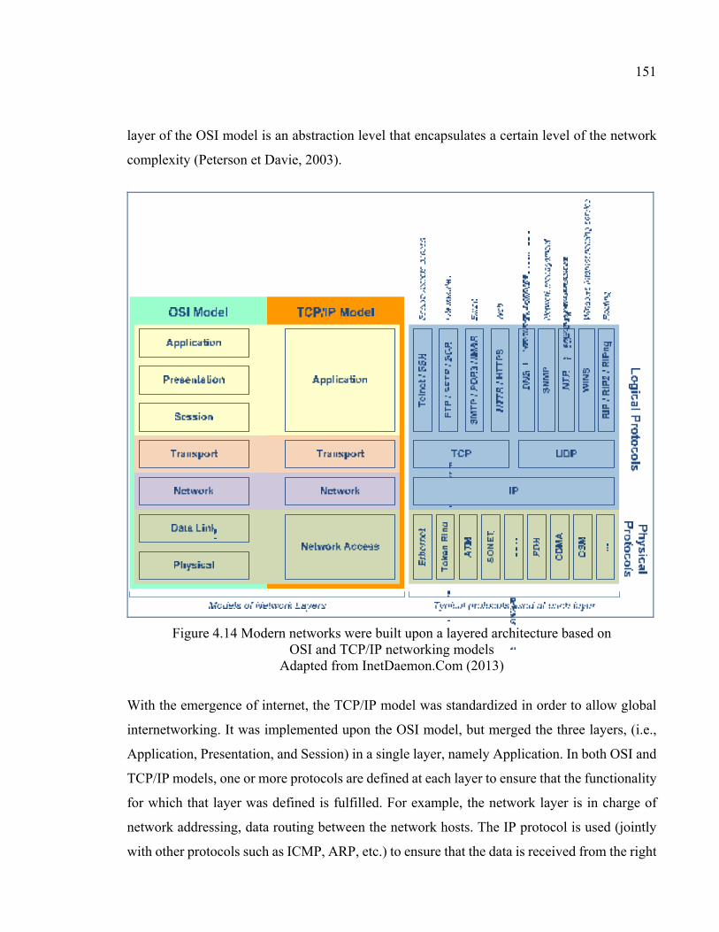
151
layer of the OSI model is an abstraction level that encapsulates a certain level of the network
complexity (Peterson et Davie, 2003).
Figure 4.14 Modern networks were built upon a layered architecture based on OSI and TCP/IP networking models
Adapted from InetDaemon.Com (2013)
With the emergence of internet, the TCP/IP model was standardized in order to allow global
internetworking. It was implemented upon the OSI model, but merged the three layers, (i.e.,
Application, Presentation, and Session) in a single layer, namely Application. In both OSI and
TCP/IP models, one or more protocols are defined at each layer to ensure that the functionality
for which that layer was defined is fulfilled. For example, the network layer is in charge of
network addressing, data routing between the network hosts. The IP protocol is used (jointly
with other protocols such as ICMP, ARP, etc.) to ensure that the data is received from the right
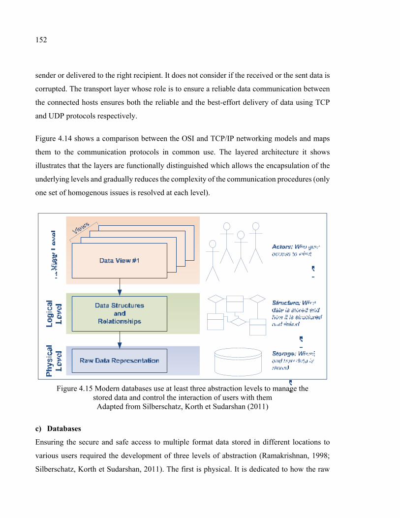
152
sender or delivered to the right recipient. It does not consider if the received or the sent data is
corrupted. The transport layer whose role is to ensure a reliable data communication between
the connected hosts ensures both the reliable and the best-effort delivery of data using TCP
and UDP protocols respectively.
Figure 4.14 shows a comparison between the OSI and TCP/IP networking models and maps
them to the communication protocols in common use. The layered architecture it shows
illustrates that the layers are functionally distinguished which allows the encapsulation of the
underlying levels and gradually reduces the complexity of the communication procedures (only
one set of homogenous issues is resolved at each level).
Figure 4.15 Modern databases use at least three abstraction levels to manage the stored data and control the interaction of users with them Adapted from Silberschatz, Korth et Sudarshan (2011)
c) Databases
Ensuring the secure and safe access to multiple format data stored in different locations to
various users required the development of three levels of abstraction (Ramakrishnan, 1998;
Silberschatz, Korth et Sudarshan, 2011). The first is physical. It is dedicated to how the raw
153
data is stored, where and how it can be retrieved. At this level, very complex low-level data
structures are used to describe the stored data in detail. The second layer is logical. It is less
complex than the physical one. It is all about what data is stored in the database and how it is
organized. This level uses human-readable and simplified data structures to capture the data
entities and the relationships between them. The third abstraction level, namely view level, is
the highest. It captures the interaction between the users and the database using the mechanism
of view. A view is a set of rules that defines which data structures are accessible by a given
user and which operations (e.g., read / write / delete) this user is authorized to conduct. All
these abstraction levels are captured in Figure 4.15.
4.2.4 Hardware Abstraction in Software Engineering
For decades, computer programming has been gradually evolving from hard coding towards
higher-level languages. Abstraction has played a key role in this evolution that enabled the
development of complex software systems. As shown in Figure 4.16, raising the abstraction
level resulted in the emergence of five generations of programming languages:
− Machine Code: The first generation was marked by machine coding using binary language.
It was platform-dependent, very tedious, time-consuming and extremely limited in terms
of productivity and outcome;
− Assembly Language: The second generation has seen the advent of assembly languages.
They are constructed of mnemonic codes which designate the basic processing commands
(e.g., ADD for addition operation) of a given machine. The resulting program is converted
into binary code using a tool called assembler. This language is easier to learn and use than
machine coding but it is not amenable for complex systems development. The developer is
in charge of all operations related to the hardware use (e.g., memory access, CPU registers
assignment, etc.);
− Structured Languages: To enhance productivity and enable better software portability, the
third generation, commonly designated as high-level languages generation, had introduced
a new level of abstraction based on data and control structures (Pierce, 2002; Sebesta,
2012). For data abstraction, the concepts of structure and data types allowed the
programmer to use both pre- and user-defined data structures to handle information. These
154
two concepts were merged into a new one: the object. Its major advantage is the possibility
of information hiding via encapsulation. For control abstraction, iterative and conditional
control flows were introduced. They served to automate controls and minimize code
duplication (Pierce, 2002). These abstraction principles enabled new development
paradigms that were defined as guidelines for software engineering (e.g., procedural,
object-oriented and extreme programming). Specialized tools such as compilers and
interpreters were used to transform programs’ source code into a platform-specific
executable binary code. In addition, depending on the programming language, these tools
may allow very useful advanced features such as automated code optimization, garbage
collection (i.e., automated dynamic memory management), managed and safe-mode code
execution, etc. All these features alleviate the developer tasks and allow the focus more on
the program than on the management of the hardware resources;
− Declarative Languages: The declarative programming languages announced the advent of
a fourth generation. These languages are intended to describe engineering systems in a way
that is similar to the structure of human language. The paradigm behind the declarative
languages aims to define computational models from which data structures and control
flows can be derived using code generation tools. This additional abstraction level
enhances models neutrality and independence from platform specificities. Declarative
languages included graphical representations (e.g., using modeling languages such as
UML) which can be transformed into source code using relevant tools;
− Problem-Solving Languages: The fifth generation of programming languages are problem
solving oriented. It provides advanced capability in using visual and graphical
representations to capture the system’s behavior, its structure and requirements, etc. The
fifth-generation programming languages were designed to fulfill a main goal: the developer
identifies problems and the computer solves them. This enables people to build relatively
complex systems without having advanced knowledge in programming. In addition, this
level of abstraction makes this generation of programming languages suitable for a broader
range of fields beyond software engineering. That is why this category of languages is
nowadays used in a myriad of other engineering systems (e.g., artificial intelligence, voice
recognition, robotics, etc.).
155
Modern software engineering addresses four major issues: (i) productivity, (ii) portability60,
(iii) interoperability61, and (iv) source code maintenance and reuse (Kleppe, Warmer et Bast,
2003; Mellor et al., 2004). The abstraction principles that have been adopted throughout the
various generations of programming languages had a significant impact on software
development:
− Hiding platform architecture to enable better portability and interoperability: Raising the
abstraction level in programming allowed to gradually separating the software from the
platform-specific attributes (e.g., architecture, instructions set, etc.). This did not only
enhanced the capability of developers to rapidly and easily implement complex software
systems without or with minor focus on hardware details but, it allowed to enhance the
portability of programs between different hardware (and/or software) platforms. In
addition, data/control abstraction support (and later modeling-centred paradigms) allowed
better interaction and interoperability between software systems regardless of hardware
and/or software differences;
− Enabling automation for better productivity: The gradual masking of hardware (and
software) environments details allowed the use of various automated tools (e.g., assembler,
compiler/interpreter, code generator, etc.) which concretely enhanced the productivity of
common software development processes. At this regard, Figure 4.17.a shows how
assemblers were designed to produce machine code for a single hardware platform while
it is nowadays possible to use the same software models to produce executable programs
for multiple hardware (and/or software) platforms. Furthermore, developers take advantage
of various automated optimization tools (e.g., memory footprint, execution time, etc.) to
enhance the quality of software systems. This progress, mainly due to the rise of abstraction
levels, saves time and money during the software development process;
60 Portability denotes the ability of using the same software system in different hardware and/or software environments. Hardware commonly involves different computer architectures while software involves generally different operating systems (or even versions of the same operating system).
61 Interoperability denotes the ability of software systems, eventually of different origins, to co-exist, interact and cooperate with other existing systems. Kleppe, Anneke G., Jos Warmer et Wim Bast. 2003. MDA Explained - The Model-driven Architecture: Practice and Promise. Addison-Wesley Longman Publishing Co., Inc., Boston, MA.
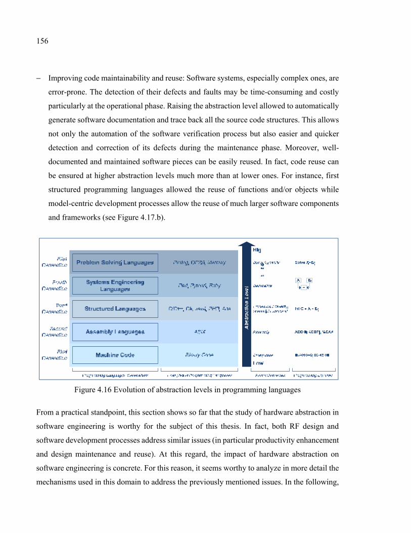
156
− Improving code maintainability and reuse: Software systems, especially complex ones, are
error-prone. The detection of their defects and faults may be time-consuming and costly
particularly at the operational phase. Raising the abstraction level allowed to automatically
generate software documentation and trace back all the source code structures. This allows
not only the automation of the software verification process but also easier and quicker
detection and correction of its defects during the maintenance phase. Moreover, well-
documented and maintained software pieces can be easily reused. In fact, code reuse can
be ensured at higher abstraction levels much more than at lower ones. For instance, first
structured programming languages allowed the reuse of functions and/or objects while
model-centric development processes allow the reuse of much larger software components
and frameworks (see Figure 4.17.b).
Figure 4.16 Evolution of abstraction levels in programming languages
From a practical standpoint, this section shows so far that the study of hardware abstraction in
software engineering is worthy for the subject of this thesis. In fact, both RF design and
software development processes address similar issues (in particular productivity enhancement
and design maintenance and reuse). At this regard, the impact of hardware abstraction on
software engineering is concrete. For this reason, it seems worthy to analyze in more detail the
mechanisms used in this domain to address the previously mentioned issues. In the following,
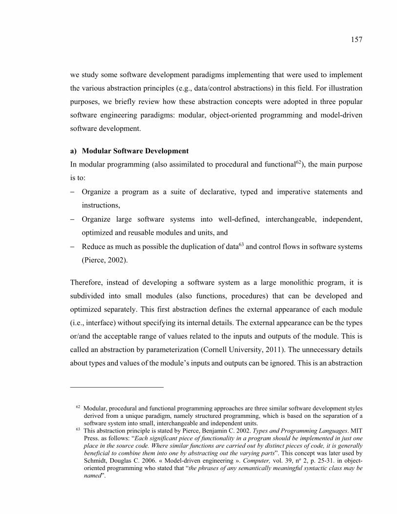
157
we study some software development paradigms implementing that were used to implement
the various abstraction principles (e.g., data/control abstractions) in this field. For illustration
purposes, we briefly review how these abstraction concepts were adopted in three popular
software engineering paradigms: modular, object-oriented programming and model-driven
software development.
a) Modular Software Development
In modular programming (also assimilated to procedural and functional62), the main purpose
is to:
− Organize a program as a suite of declarative, typed and imperative statements and
instructions,
− Organize large software systems into well-defined, interchangeable, independent,
optimized and reusable modules and units, and
− Reduce as much as possible the duplication of data63 and control flows in software systems
(Pierce, 2002).
Therefore, instead of developing a software system as a large monolithic program, it is
subdivided into small modules (also functions, procedures) that can be developed and
optimized separately. This first abstraction defines the external appearance of each module
(i.e., interface) without specifying its internal details. The external appearance can be the types
or/and the acceptable range of values related to the inputs and outputs of the module. This is
called an abstraction by parameterization (Cornell University, 2011). The unnecessary details
about types and values of the module’s inputs and outputs can be ignored. This is an abstraction
62 Modular, procedural and functional programming approaches are three similar software development styles derived from a unique paradigm, namely structured programming, which is based on the separation of a software system into small, interchangeable and independent units.
63 This abstraction principle is stated by Pierce, Benjamin C. 2002. Types and Programming Languages. MIT Press. as follows: “Each significant piece of functionality in a program should be implemented in just one place in the source code. Where similar functions are carried out by distinct pieces of code, it is generally beneficial to combine them into one by abstracting out the varying parts”. This concept was later used by Schmidt, Douglas C. 2006. « Model-driven engineering ». Computer, vol. 39, no 2, p. 25-31. in object-oriented programming who stated that “the phrases of any semantically meaningful syntactic class may be named”.
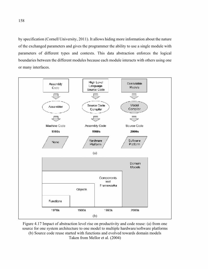
158
by specification (Cornell University, 2011). It allows hiding more information about the nature
of the exchanged parameters and gives the programmer the ability to use a single module with
parameters of different types and contexts. This data abstraction enforces the logical
boundaries between the different modules because each module interacts with others using one
or many interfaces.
(a)
(b)
Figure 4.17 Impact of abstraction level rise on productivity and code reuse: (a) from one source for one system architecture to one model to multiple hardware/software platforms
(b) Source code reuse started with functions and evolved towards domain models Taken from Mellor et al. (2004)
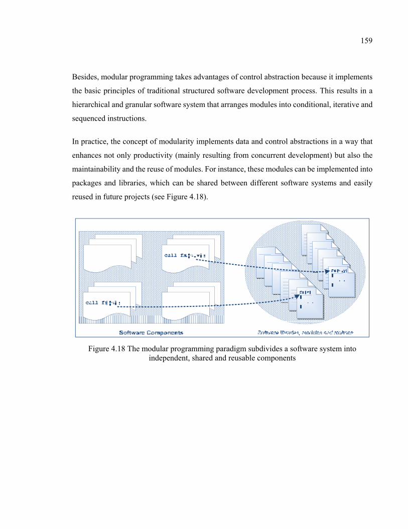
159
Besides, modular programming takes advantages of control abstraction because it implements
the basic principles of traditional structured software development process. This results in a
hierarchical and granular software system that arranges modules into conditional, iterative and
sequenced instructions.
In practice, the concept of modularity implements data and control abstractions in a way that
enhances not only productivity (mainly resulting from concurrent development) but also the
maintainability and the reuse of modules. For instance, these modules can be implemented into
packages and libraries, which can be shared between different software systems and easily
reused in future projects (see Figure 4.18).
Figure 4.18 The modular programming paradigm subdivides a software system into independent, shared and reusable components
160
b) Object-Oriented Programming64
The object-oriented approach was introduced as an extension of traditional programming
paradigms (e.g., modular programming). On the one hand, it aimed to reduce the coupling65
between and improve the cohesion66 within modules in these conventional approaches
(Schach, 2002). On the other hand, it was meant to bring more abstraction in order to enhance
the maintainability67 and reusability of large software systems (Kendal, 2011).
To do so, the object-oriented programming approach has defined a fundamental concept,
namely object (i.e., practically an instantiation of a class) which is a model that describes the
properties (and attributes) of a real-world entity and the operations (and actions) that can be
performed on or by that entity (Koffman et Wolfgang, 2006). An object is not only meant to
keep the real-world entity relevant features, properties and functions and discard those
irrelevant ones but it also allows to control their visibility and their scope as well as the
relationships (and the interactions) that the object may have with other objects. To make this
concept effective, various abstraction techniques were defined:
• Data Abstraction: Inheritance, Generalization and Specialization
An object is an abstraction of a real-world entity. It captures both its intrinsic attributes and
behavior. This representation ignores the irrelevant entity details and focuses only on its main
characteristics. An object can inherit the properties and operations of one or many other
objects. The inherited object (i.e., parent class) is a generalization of the inheriting one (i.e.,
child class). Generalization allows defining generic objects that have common properties
64 For extensive information about object-oriented programming principles, the reader may refer to Baldwin, Douglas, et Greg W. Scragg. 2004. The Object Primer. Cambridge University Press. and Klump, R. 2001. « Understanding Object-Oriented Programming Concepts ». In IEEE Power Engineering Society Summer Meeting. (Vancouver, 15 Jul 2001-19 Jul 2001 ). Vol. 2, p. 1070-1074. < http://ieeexplore.ieee.org/ielx5/7659/20923/00970207.pdf?tp=&arnumber=970207&isnumber=20923 >.
65 The concept of coupling refers to the degree of interdependence of a software module with other modules. Schach, Stephen R. 2002. Object-oriented and Classical Software Engineering, 6. McGraw-Hill New York.
66 The concept of cohesion characterizes the degree of interdependence between the elements of the same module. High cohesion results in better software robustness, reliability and reusability ibid.. High cohesion often correlates with low coupling and vice versa.
67 Maintainability is a crucial property in software development because 70% of the cost is incurred during the software usage phase Kendal, Simon. 2011. Object Oriented Programming Using C#. Simon Kendal & Ventus Publishing.

161
(Kendal, 2011). On the contrary, the inheriting object is a specialization of the inherited one.
Specialization enables the creation of objects with specific properties from generic ones. In
practice, it takes place using the inheritance mechanism and extending the attributes and the
behavior of the object. Thus, inheritance removes data and code redundancy. It enables the
extensibility and the reusability of objects. In addition, it is possible to define various types of
relationships between objects (e.g., generalization, composition, association68, dependency69,
etc.). The semantic of each relationship is determined by the logical link tying the objects in
the real world. For instance, generalization translates an “is a” relationship (which roughly
means that the child object is a “copy” of the parent one).
To illustrate these, Figure 4.19.a shows entities from the real world. In Figure 4.19.b, the
properties, operations and relationships linking these objects are captured in a class diagram70.
In this example, a bus, a car or a truck is a vehicle. That is a generalization relationship between
the bus, the car and the truck objects at one side and the vehicle object at the other one. A
vehicle has a given number of tires. This is a composition relationship between the vehicle and
the tire objects. In addition, speed, weight and color are some of the attributes of a vehicle.
Parking, moving forward and backward are some of its operations. These attributes and
operations are naturally inherited by the car, the bus and the truck. However, loading and
unloading passengers and cargo are specific to the bus and the truck respectively. The
transmission type is specific to the car. These additional specificities make the car, the bus and
the truck objects a specialization of the vehicle one.
68 Association defines a relationship in which an object A uses an object B as part of its behavior Wong, Stephen, et Dung Nguyen. 2008. Principles of Object-Oriented Programming. Connexions (Rice University).
69 Dependency defines a relationship in which an object A depends on an object B ibid. 70 A Class Diagram is a UML structural diagram that captures the attributes, operations and relationships
between objects.
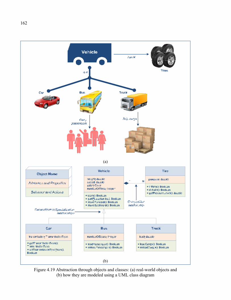
162
(a)
(b)
Figure 4.19 Abstraction through objects and classes: (a) real-world objects and (b) how they are modeled using a UML class diagram
163
• Control Abstraction (aka Procedural Abstraction): Encapsulation and Polymorphism
The object-oriented programming approach adopts the principle of separation between what
should be achieved by an object (or its attributes/operations) and how it should be achieved
(Koffman et Wolfgang, 2006). This principle is implemented through the mechanism of
encapsulation (Kendal, 2011). This mechanism consists of hiding both object data (i.e.,
attributes) and implementation (i.e., operations) and providing an appropriate interface for it.
This interface defines which attributes and/or operations are accessible and how they can be
used (using access modifiers71 such as private, protected and public, etc.). Thus, the interaction
with the object takes place using its interface that reduces the implementation complexity.
Another important mechanism in control abstraction is polymorphism, which denotes the
ability of using an object regardless of its specificities. In practice, this means that the object
has more than one type and can be used in multiple contexts without any code duplication. It
is defined as an object with abstract attributes and operations to which a specific type is
associated during usage. Abstract data types72 are an example of what can be achieved using
the mechanism of polymorphism.
In summary, the concept of object modeling added to the various mechanisms of hierarchy,
encapsulation, and polymorphism brought abstraction to a higher level in object-oriented
software development processes. The impact of this rise of abstraction level on the various
software metrics (especially maintainability and reusability) is concrete. At this regard, it is
proven that object-oriented approach results in more maintainable and reusable software
systems than the traditional structured software approaches (e.g., modular) (Henry et Lattanzi,
1994; Lee et Chang, 2000).
71 An access modifier sets the accessibility level for object attributes and operations. For example, a “private” modifier (minus “-” sign in UML class) grants access only to the attributes and operations while a “public” modifier (plus “+” sign in UML class) allows all objects to access that attribute/operation.
72 An Abstract Data Type (ADT) is a data structure whose type is not explicitly defined. It takes the type of the operation performed in a given context.
164
c) Model-Driven Engineering (MDE)
The third-generation programming languages (particularly modular and object-oriented) have
raised the level of abstraction of the programming environment which allowed the use of
automated tools (such as assemblers, compilers and preprocessors) to automate the generation
of executable routines (e.g., machine code) from relatively high-level programming software
constructs (e.g., source code, UML diagrams) (Frankel, 2003; Mellor, Balcer et Foreword By-
Jacoboson, 2002; Schmidt, 2006). This is also due to operating systems which have raised the
level of abstraction of the computing platform and hided unnecessary hardware details
(Frankel, 2003). Then, compilers do not generate all the required machine code but should
henceforth rely on the OS73 services and routines to partly do this. In addition, special
middleware components (e.g., application virtual machines74, run-time systems) came into
play to enhance code portability between platforms (i.e., using CPU- and OS-independent
intermediate code). Over time, the complexity of the underlying software platforms (especially
OS services and middleware) has rapidly grown. This, combined to a slow evolution of
general-purpose languages towards an effective capture of platform-specific artifacts and
expression of specialized domain concepts, has increased the difficulty of porting source code
between different (/versions of the same) software platforms. At this regard, modern platforms’
complexity reached a ceiling at which the development of large software systems became
costly and time-consuming, especially due to the manual code porting, integration and
maintenance (Schmidt, 2006). So, if hardware-platform independence was ensured mostly
using relevant OS and middleware to enable code execution on various hardware platforms
with almost no changes, new paradigms with higher abstraction levels are required to enable
the execution of the same source code on different software platforms with no or at least minor
changes (i.e., software-platform independence) (Mellor et al., 2004). This new abstraction level
is not only expected to mask the growing complexity of existent and emerging software
platforms but should also enable the development of expressive software models that can be
73 Paragraph 4.2.3.a explains how software applications use the OS and middleware resources through the mechanism of system calls.
74 Application Virtual Machines (and run-time systems) are software components that create a (hardware and/or software) platform-independent programming environment to enable the interpretation (or just-in-time compilation) and execution of intermediate code.
165
mapped at the same time to different environments with no changes. Thus, applications
intended for CORBA75, client-server relational databases or web platforms are expected to be
derived from the same high-level software models (Mellor et al., 2004).
To bridge the gap between the increasing complexity of software (/hardware) platforms and
the limitations of third-generation programming paradigms, a new software development
methodology, namely Model-Driven Engineering76 (MDE), has emerged in the early 2000s.
MDE is all “about the use of relevant abstractions that help people focus on key details of a
complex problem or solution combined with automation to support the analysis of both the
problem and solution (…)” (Blackburn, 2008, p. 7). To raise further the abstraction level in
software engineering, MDE focuses on the creation of models which are close to the problem
domain and using more abstract and expressive concepts (Milicev, 2009). It is worth noting
that, in MDE, abstraction and modeling are interrelated. On the one hand, MDE considers
abstraction as the capability of finding out the commonality in many different observations
(i.e., viewpoints) (Brambilla, Cabot et Wimmer, 2012). This implies the ability of generalizing
specific features of real-world objects, the classification of these objects into coherent groups
and clusters and the aggregation of these them into more complex ones (Brambilla, Cabot et
Wimmer, 2012). On the other hand, modeling is the process of representing real-world entities
as simplified and understandable representations. At this regard, abstraction helps making the
good decisions about what should be captured and what should be removed in a model
(Fernandes). From this viewpoint, MDE considers a model as an abstraction of a reality. It is
an entity that hides some aspects of this reality while it stresses other ones.
75 CORBA stands for Common Object Request Broker Architecture which is an OMG standard that is intended to facilitate the communication, collaboration and interaction between different platforms regardless of their hardware and software architectures.
76 Model-Driven Engineering is sometimes referred to as Model-Driven Development (MDD) Teppola, S., P. Parviainen et J. Takalo. 2009. « Challenges in the Deployment of Model Driven Development ». In Fourth International Conference on Software Engineering Advances. (Porto 20-25 Sept. 2009 ), p. 15-20. <http://ieeexplore.ieee.org/ielx5/5298192/5298193/05298434.pdf?tp=&arnumber=5298434&isnumber=5298193 >. In fact, most terms with the prefix “model-driven” designate software development approaches based on intensive modeling activity Embley, David W., et Bernhard Thalheim. 2011. Handbook of Conceptual Modeling: Theory, Practice, and Research Challenges. Springer.
166
Since MDE addresses a broad range of problems, it considers that “everything is a model”
(Bézivin, 2005). This definition suggests that not only the problem can be modeled but also its
solution. In practice, every abstraction level and each design step (e.g., specifications, design,
implementation, etc.) can be associated to one or many models. To change the abstraction level
or move from a design step to another, new models should be derived from those defined at
the previous abstraction level (respectively design step). This standpoint is interesting in a
sense that a complex system can be developed starting by very-low complexity models which
can be gradually refined to include more details through the design cycle. In addition, this does
not only help mastering the system’s complexity but also enhances productivity if automated
model-to-model transformation is possible. For instance, when MDE is applied to software
development, the typical lifecycle illustrated in Figure 4.20, emphasizes the use of automation
tools in order to derive the appropriate models required at each design step.
From the beginning, MDE was thought as a generic design approach that is not limited only to
software engineering. It defines key abstraction and automation concepts that are amenable for
use in various engineering fields. What fueled this tendency is the fact that software systems
are increasingly being developed in multi-disciplinary projects. Moreover, this approach is
being already used in different areas (e.g., software-defined radio (Trask et al., 2006), voice
recognition (Briand, 2005), embedded and real-time systems (David et Nielsen, 2008; Hsiung
et al., 2009)). In software engineering, MDE is gaining growing interest. For instance, at least
three major initiatives were proposed as guidelines for the practical implementation of model-
driven engineering concepts:
1. Model-Driven Architecture (MDA)77,
2. Model-Driven Software Development (MDSD)78, and
77 For detailed presentation of MDA, the reader may refer to Kleppe, Anneke G., Jos Warmer et Wim Bast. 2003. MDA Explained - The Model-driven Architecture: Practice and Promise. Addison-Wesley Longman Publishing Co., Inc., Boston, MA., Frankel, David S. 2003. Model Driven Architecture: Applying MDA to Enterprise Computing. John Wiley and Sons. and Poole, John D. 2001. « Model-Driven Architecture: Vision, Standards and Emerging Tools ». In Workshop on Metamodeling and Adaptive Object Models. < http://www.omg.org/mda/mda_files/Model-Driven_Architecture.pdf >.
78 For more information about MDSD, the reader may refer to Völter, Markus, Thomas Stahl, Jorn Bettin, Arno Haase et Simon Helsen. 2006. Model-Driven Software Development: Technology, Engineering,
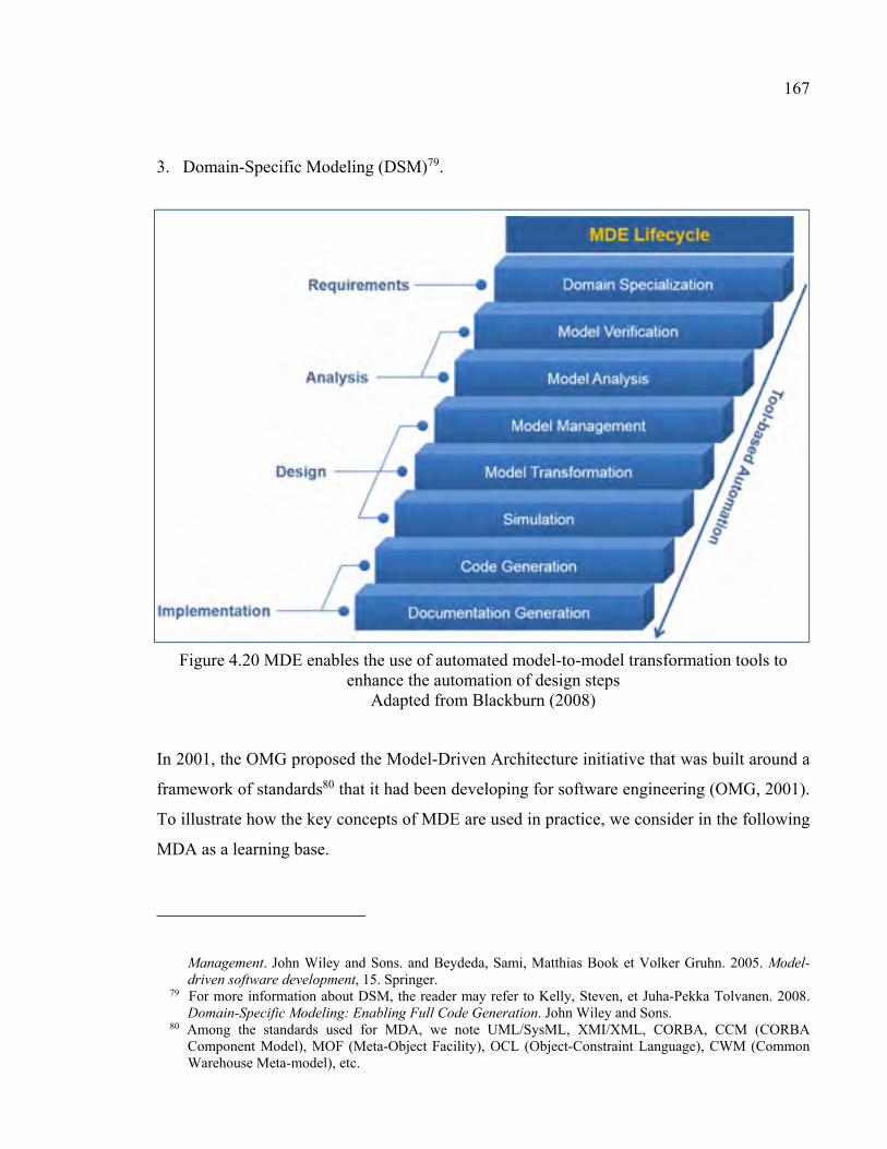
167
3. Domain-Specific Modeling (DSM)79.
Figure 4.20 MDE enables the use of automated model-to-model transformation tools to enhance the automation of design steps
Adapted from Blackburn (2008)
In 2001, the OMG proposed the Model-Driven Architecture initiative that was built around a
framework of standards80 that it had been developing for software engineering (OMG, 2001).
To illustrate how the key concepts of MDE are used in practice, we consider in the following
MDA as a learning base.
Management. John Wiley and Sons. and Beydeda, Sami, Matthias Book et Volker Gruhn. 2005. Model-driven software development, 15. Springer.
79 For more information about DSM, the reader may refer to Kelly, Steven, et Juha-Pekka Tolvanen. 2008. Domain-Specific Modeling: Enabling Full Code Generation. John Wiley and Sons.
80 Among the standards used for MDA, we note UML/SysML, XMI/XML, CORBA, CCM (CORBA Component Model), MOF (Meta-Object Facility), OCL (Object-Constraint Language), CWM (Common Warehouse Meta-model), etc.
168
• Models and Meta-Models
In MDA, models are the masterpieces in software design cycle. They are used to capture not
only the system’s structure and behavior but also timing constraints and environment resources
(Blackburn, 2008). To represent all these system aspects with respect to abstraction and
consistency requirements, models can be (Fernandes):
− Horizontal: if they capture different system aspects which are considered at the same level
of abstraction, or
− Vertical: if they describe system aspects that are considered at different levels of
abstraction.
From system standpoint, models can be classified into various types (Fernandes):
− State-oriented: to capture the system’s dynamic behavior,
− Activity-oriented: to describe the system as a sequence of activities,
− Structure-oriented: to characterize the system’s physical structure (including interfaces and
ports),
− Data-oriented: to describe the system as a collection of data that is related by their attributes
and classifications,
− Heterogeneous: to incorporate a mix of the previous four characteristics.
From platform standpoint, models can be classified into (Frankel, 2003):
− Business/Domain-specific: describes the domain-specific aspects regardless of automation
ability,
− System: captures the aspects that can be used to automate domain-specific elements,
− Logical: describes the system’s logic including its behavioral and structural aspects,
− Physical: captures the system’s physical artifacts and its related environment resources,
− Requirements: captures the same attributes as the logical model but in a computation-
independent manner (i.e., no technology aspects are considered),
− Computational: augments to the logical model with additional domain-specific technical
information,
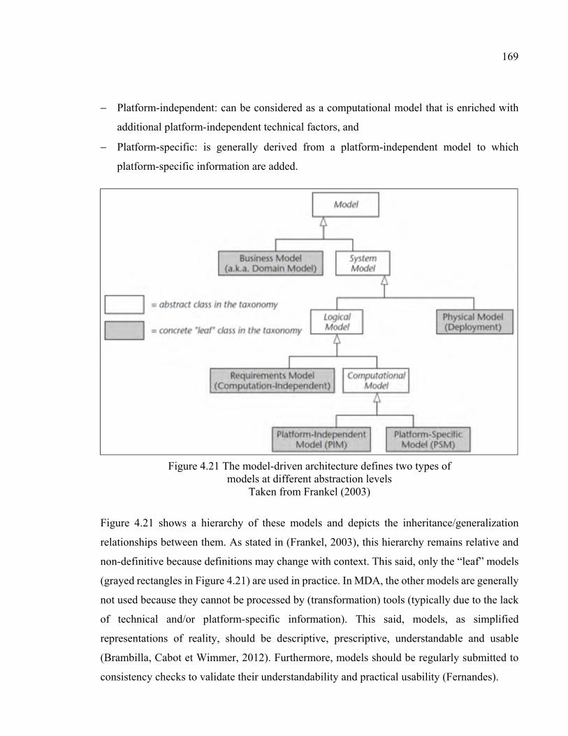
169
− Platform-independent: can be considered as a computational model that is enriched with
additional platform-independent technical factors, and
− Platform-specific: is generally derived from a platform-independent model to which
platform-specific information are added.
Figure 4.21 The model-driven architecture defines two types of models at different abstraction levels
Taken from Frankel (2003)
Figure 4.21 shows a hierarchy of these models and depicts the inheritance/generalization
relationships between them. As stated in (Frankel, 2003), this hierarchy remains relative and
non-definitive because definitions may change with context. This said, only the “leaf” models
(grayed rectangles in Figure 4.21) are used in practice. In MDA, the other models are generally
not used because they cannot be processed by (transformation) tools (typically due to the lack
of technical and/or platform-specific information). This said, models, as simplified
representations of reality, should be descriptive, prescriptive, understandable and usable
(Brambilla, Cabot et Wimmer, 2012). Furthermore, models should be regularly submitted to
consistency checks to validate their understandability and practical usability (Fernandes).
170
To ensure that models yield a common understanding between all the involved parties (either
human- or computer-based), they should comply with common semantics and rules (Mellor et
al., 2004). The “language” in which a model is defined is called meta-model. In fact, it is simply
a “model that defines the structure, semantics, and constraints for a family of models” (Mellor
et al., 2004, p. 14). It is a “model of models”.
From an abstraction standpoint, if models are constructed as previously mentioned using the
mechanisms of classification, generalization and aggregation, in a way that produces a simple
but expressive representation of reality, meta-models that define the guideline semantics of
models are themselves another abstraction layer. The example illustrated in Figure 4.22 shows
how these concepts can be applied in practice. An immediate (i.e., “first-order”) abstraction of
the represented pets is the capture of their individual attributes (e.g., name, species, weight). A
more elaborate abstraction of this is the capture of the common attributes among the different
first-order representation. This results in a classification of these pets (i.e., captured in a typical
class model). So, how to ensure that this class model is understood by everyone in the same
way? For this purpose, a meta-model was created to define the relationships between a “class”
and a “property” (e.g., generalization, association, etc.). The subsequent interpretation to this
hierarchy of abstractions enables everyone to easily understand that a cat “is a” pet (i.e.,
“class”) that “has a” given “property” which distinguishes it from the other pets. The reader
may note here the same taxonomy we have already presented in Figure 4.19.
In MDA, models can be developed using UML. However, the developer can use any other
modeling language for modeling. For instance, domain-specific languages (DSL) are used to
capture domain-specific artifacts and particularities that UML cannot explicitly express (Van
Deursen, Klint et Visser, 2000). Meta-models are commonly defined using meta-modeling
languages (e.g. OMG’s Meta-Object Facility81, Query/Views/Transformations82).
81 Meta-Object Facility (MOF) is an OMG standard for the creation, manipulation and exchange of interoperable meta-models.
82 Query/Views/Transformations (QVT) is an OMG standard set of languages for creating query models, views and transformations.
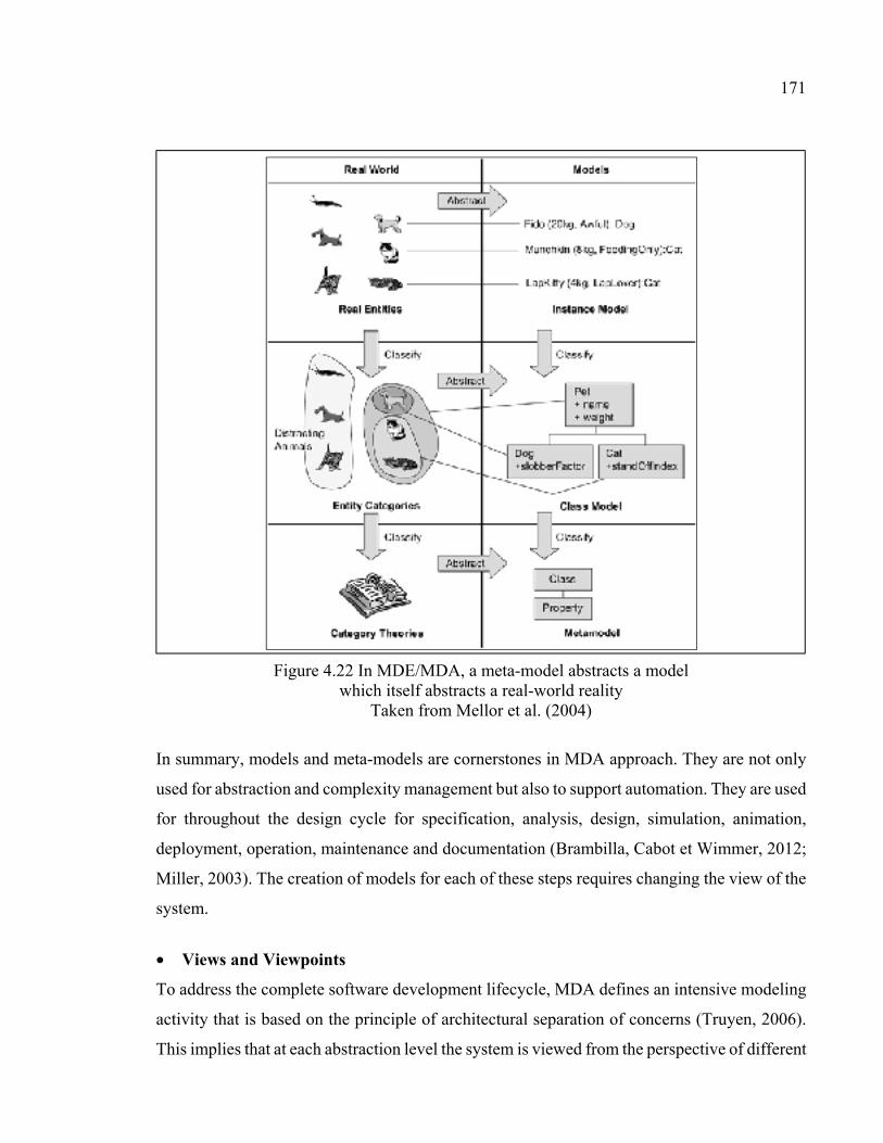
171
Figure 4.22 In MDE/MDA, a meta-model abstracts a model which itself abstracts a real-world reality
Taken from Mellor et al. (2004)
In summary, models and meta-models are cornerstones in MDA approach. They are not only
used for abstraction and complexity management but also to support automation. They are used
for throughout the design cycle for specification, analysis, design, simulation, animation,
deployment, operation, maintenance and documentation (Brambilla, Cabot et Wimmer, 2012;
Miller, 2003). The creation of models for each of these steps requires changing the view of the
system.
• Views and Viewpoints
To address the complete software development lifecycle, MDA defines an intensive modeling
activity that is based on the principle of architectural separation of concerns (Truyen, 2006).
This implies that at each abstraction level the system is viewed from the perspective of different
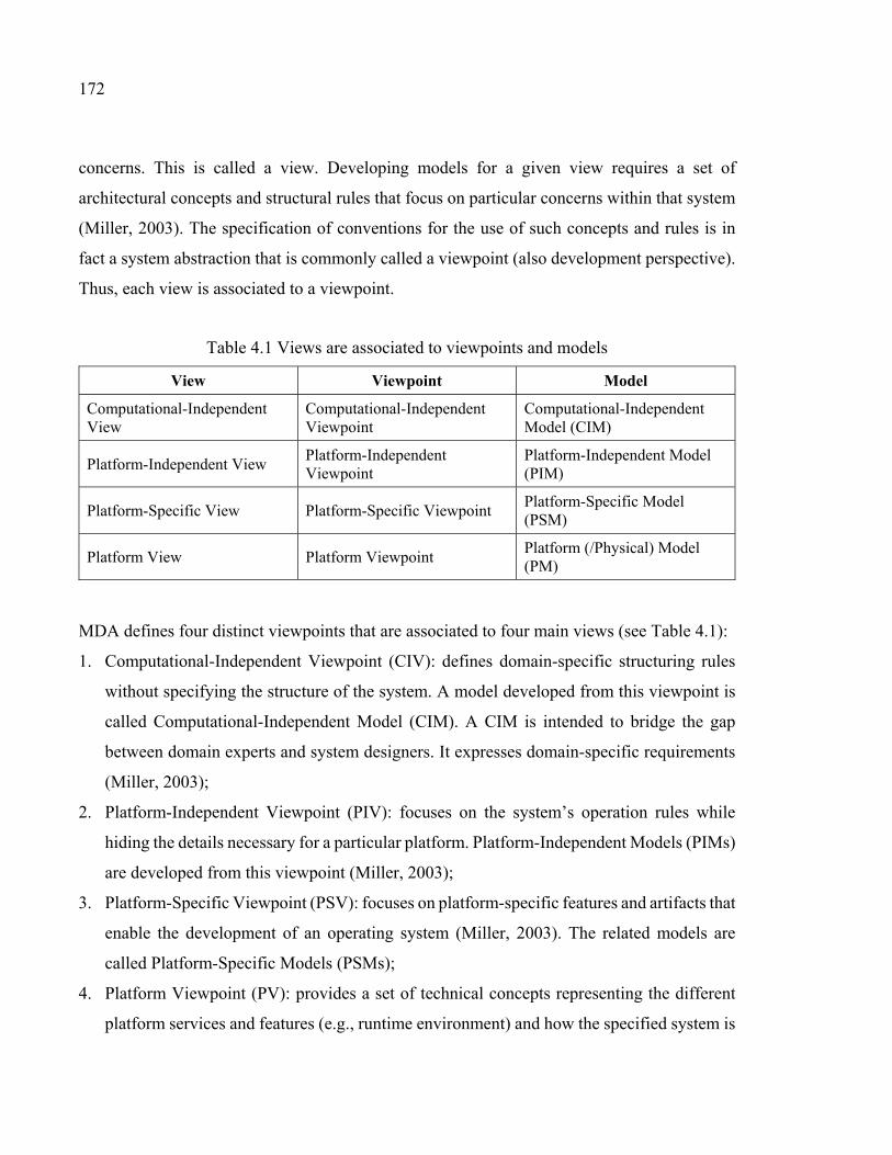
172
concerns. This is called a view. Developing models for a given view requires a set of
architectural concepts and structural rules that focus on particular concerns within that system
(Miller, 2003). The specification of conventions for the use of such concepts and rules is in
fact a system abstraction that is commonly called a viewpoint (also development perspective).
Thus, each view is associated to a viewpoint.
Table 4.1 Views are associated to viewpoints and models
View Viewpoint Model
Computational-Independent View
Computational-Independent Viewpoint
Computational-Independent Model (CIM)
Platform-Independent View Platform-Independent Viewpoint
Platform-Independent Model (PIM)
Platform-Specific View Platform-Specific Viewpoint Platform-Specific Model (PSM)
Platform View Platform Viewpoint Platform (/Physical) Model (PM)
MDA defines four distinct viewpoints that are associated to four main views (see Table 4.1):
1. Computational-Independent Viewpoint (CIV): defines domain-specific structuring rules
without specifying the structure of the system. A model developed from this viewpoint is
called Computational-Independent Model (CIM). A CIM is intended to bridge the gap
between domain experts and system designers. It expresses domain-specific requirements
(Miller, 2003);
2. Platform-Independent Viewpoint (PIV): focuses on the system’s operation rules while
hiding the details necessary for a particular platform. Platform-Independent Models (PIMs)
are developed from this viewpoint (Miller, 2003);
3. Platform-Specific Viewpoint (PSV): focuses on platform-specific features and artifacts that
enable the development of an operating system (Miller, 2003). The related models are
called Platform-Specific Models (PSMs);
4. Platform Viewpoint (PV): provides a set of technical concepts representing the different
platform services and features (e.g., runtime environment) and how the specified system is
173
connected to them (Miller, 2003). The related models are called platform (also physical)
models.
Views and viewpoints are interrelated. However, to be effective, they require some notions to
be defined (mostly depending on the context). For example, we cite:
− Independence: it is defined, in the context of MDA, as the “quality that the model does not
call for the support of a platform of a particular type [or relying on particular features]”
(Miller, 2003, p. 31);
− Platform: in MDA, the notion of platform is the most floating due to the existence of myriad
different frameworks that can be considered as such. That is why according to (Miller,
2003), the OMG did not include a deliberate definition of platform in MDA standard.
However, there were a number of attempts to define the term such as (Beydeda, Book et
Gruhn, 2005) who considers a platform as “a set of subsystems and technologies that
provide the capabilities needed to support the execution of a software application” (p.
121);
− System: it is often defined as “a set of parts, connected and interrelated, forming a complex
whole” (Miller, 2003, p. 12). In software domain, a system may be defined as one or many
applications supported by one or many (hardware and/or software) platforms.
As previously mentioned, the four MDA views/viewpoints result in four key models that
represent the fundamental ingredients of the software design approach:
1. Computational-Independent Model (CIM): it expresses business-/domain-specific
concerns and often uses an expert vocabulary to express the system’s specifications without
any reference to platform and technology information (Almeida, 2008). It is considered as
a contractual reference that is elaborated to capture high-level client requirements
(Almeida, 2008; Baudry, Nebut et Le Traon, 2007);
2. Platform-Independent Model (PIM): it deals with the constraints that a system requires to
be properly implemented. The PIM remains independent from the underlying technology
(e.g., OS, programming frameworks, middleware, etc.) (Almeida, 2008);
174
3. Platform-Specific Model (PSM): it describes the system with regard to platform- and
language-specific elements (e.g., class model, schema model, interface code model,
database model, etc.) (Almeida, 2008);
4. Platform Model (PM): it is also called physical model. It provides physical artifacts and
resources used during runtime (e.g., source code, executable, libraries, etc.) (Frankel,
2003).
As shown in Figure 4.23, these four models correspond to four distinct abstraction levels. The
CIM and PM are considered respectively as the highest and lowest levels of abstraction. For
each CIM (i.e., requirements/domain-specific model), a PIM is defined. From each PIM,
multiple PSMs and PMs (i.e., implementations) can be derived. MDA considers the automated
generation of models at a given abstraction level from the upper (and/or lower) ones using a
mechanism of model-to-model transformation. Relevant tools use this mechanism to automate
as much as possible the software development process.
• Transformations and Mappings
As explained in the previous section, MDA divides software development process into two
main areas: (i) platform-independent, including CIM and PIM where models are meant to be
independent from technology information and (ii) platform-specific, including PSMs and PMs,
where models target specific execution platforms and runtime environments. MDA uses
model-to-model transformations to enable the transition between the various types of models
and thus move the system design from one abstraction level to another (i.e., from specification
to implementation) (Fernandes).
A model-to-model transformation is the process of converting a source model conforming to a
given meta-model to a target model conforming to a given meta-model as well, either at the
same abstraction level or at a different one (Miller, 2003). This process relies on a
transformation mechanism composed of two main elements (Pastor et Molina, 2007):
1. Mappings: establish relationships between elements in the source model and their
counterparts in the target model. Their goal is to characterize how elements in the latter
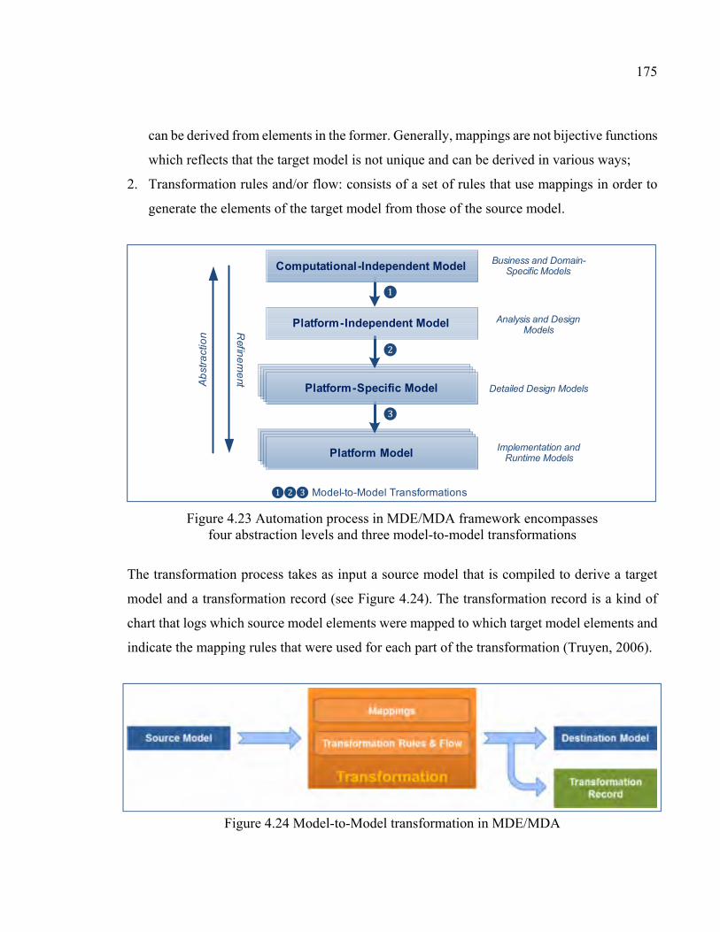
175
can be derived from elements in the former. Generally, mappings are not bijective functions
which reflects that the target model is not unique and can be derived in various ways;
2. Transformation rules and/or flow: consists of a set of rules that use mappings in order to
generate the elements of the target model from those of the source model.
Business and Domain-Specific Models
Platform Model
Platform-Specific Model
Platform-Independent Model
Computational-Independent Model
Ab
stra
ctio
n
Refin
em
ent
❶❷❸
❶❷❸ Model-to-Model Transformations
Analysis and Design Models
Detailed Design Models
Implementation and Runtime Models
Figure 4.23 Automation process in MDE/MDA framework encompasses four abstraction levels and three model-to-model transformations
The transformation process takes as input a source model that is compiled to derive a target
model and a transformation record (see Figure 4.24). The transformation record is a kind of
chart that logs which source model elements were mapped to which target model elements and
indicate the mapping rules that were used for each part of the transformation (Truyen, 2006).
Figure 4.24 Model-to-Model transformation in MDE/MDA
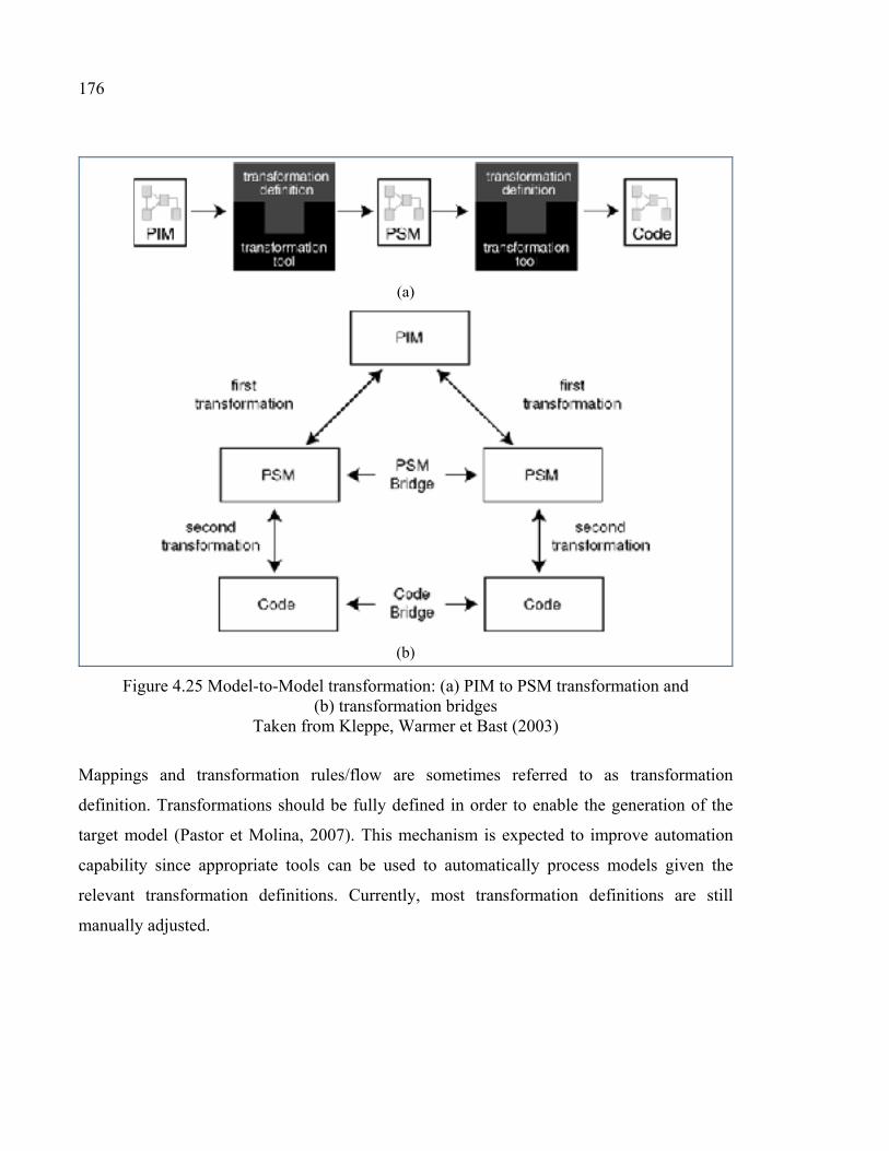
176
(a)
(b)
Figure 4.25 Model-to-Model transformation: (a) PIM to PSM transformation and (b) transformation bridges
Taken from Kleppe, Warmer et Bast (2003)
Mappings and transformation rules/flow are sometimes referred to as transformation
definition. Transformations should be fully defined in order to enable the generation of the
target model (Pastor et Molina, 2007). This mechanism is expected to improve automation
capability since appropriate tools can be used to automatically process models given the
relevant transformation definitions. Currently, most transformation definitions are still
manually adjusted.
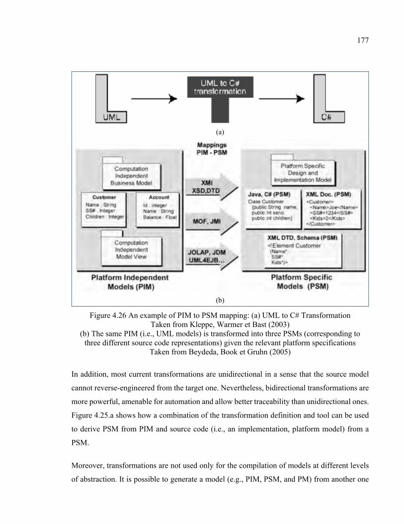
177
(a)
(b)
Figure 4.26 An example of PIM to PSM mapping: (a) UML to C# Transformation Taken from Kleppe, Warmer et Bast (2003)
(b) The same PIM (i.e., UML models) is transformed into three PSMs (corresponding to three different source code representations) given the relevant platform specifications
Taken from Beydeda, Book et Gruhn (2005)
In addition, most current transformations are unidirectional in a sense that the source model
cannot reverse-engineered from the target one. Nevertheless, bidirectional transformations are
more powerful, amenable for automation and allow better traceability than unidirectional ones.
Figure 4.25.a shows how a combination of the transformation definition and tool can be used
to derive PSM from PIM and source code (i.e., an implementation, platform model) from a
PSM.
Moreover, transformations are not used only for the compilation of models at different levels
of abstraction. It is possible to generate a model (e.g., PIM, PSM, and PM) from another one
178
which often serves for the refinement of that model (Fernandes). The transformation used for
this purpose is commonly called a “bridge” (Kleppe, Warmer et Bast, 2003). Transformation
bridges (see Figure 4.25.b) enable interoperability (i.e., a major goal of MDA) because they
allow the creation of multiple PSMs (respectively PMs) for different platforms from a single
PIM (respectively PSM) (Kleppe, Warmer et Bast, 2003).
4.2.5 Hardware Abstraction in Other Domains
We have studied so far how hardware abstraction applies to digital and analog/mixed-signal
design, some computer-based systems (e.g., operating systems, databases, networking) and
software engineering. It is worth noting that this concept was not limited to these domains but
was adopted in a myriad of other domains. In the following, we briefly present two examples
of recent hardware abstraction strategies that were used for the development of software-
defined radios systems and applications.
a) Software Communication Architecture (SCA) and its Modem Hardware Abstraction
Layer (MHAL)
The Software Communication Architecture (SCA) is a core framework that was developed by
the Joint Tactical Radio System83 (JTRS) to standardize the development of software-defined
radios for both military and civil applications (Aguayo Gonzalez, Portelinha et Reed, 2007). It
was designed to provide standard application-layer interfaces and services that allow
waveforms to run on different hardware platforms (Lind et Littke, 2004). It particularly
implements CORBA-based services in order to enable the portability of software code among
hardware platforms and the interoperability between heterogeneous systems. In fact, hardware
platforms addressed by SCA are mostly limited to GPPs and does not extend this service to
digital signal processing platforms (such as DSP and FPGA) (Dackenberg, 2010). For this
reason, it was augmented with a special abstraction layer, namely Modem Hardware
Abstraction Layer (MHAL) (JTRS, 2010), which implements a standard messaging structure
83 The Joint Tactical Radio System is a US defense program for the development and acquisition of next-generation voice-and-data radio for military use.
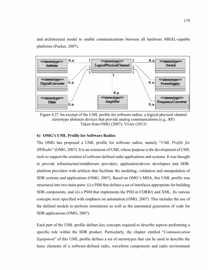
179
and architectural model to enable communications between all hardware MHAL-capable
platforms (Pucker, 2007).
Figure 4.27 An excerpt of the UML profile for software radios: a logical-physical channel stereotype abstracts devices that provide analog communications (e.g., RF)
Taken from OMG (2007); Vivier (2013)
b) OMG’s UML Profile for Software Radios
The OMG has proposed a UML profile for software radios, namely “UML Profile for
SWRadio” (OMG, 2007). It is an extension of UML whose purpose is the development of UML
tools to support the creation of software-defined radio applications and systems. It was thought
to provide infrastructure/middleware providers, application/device developers and SDR-
platform providers with artifacts that facilitate the modeling, validation and manipulation of
SDR systems and applications (OMG, 2007). Based on OMG’s MDA, this UML profile was
structured into two main parts: (i) a PIM that defines a set of interfaces appropriate for building
SDR components, and (ii) a PSM that implements the PIM in CORBA and XML. Its various
concepts were specified with emphasis on automation (OMG, 2007). This includes the use of
the defined models to perform simulations as well as the automated generation of code for
SDR applications (OMG, 2007).
Each part of the UML profile defines key concepts required to describe aspects performing a
specific role within the SDR product. Particularly, the chapter entitled “Communication
Equipment” of this UML profile defines a set of stereotypes that can be used to describe the
basic elements of a software-defined radio, waveform components and radio environment
180
(Vivier, 2013). It allows for example the description of the SDR building blocks and the
relationships between them (OMG, 2007; Vivier, 2013). For instance, RF devices are modeled
using stereotypes such as the LogicalPhysicalChannel (see Figure 4.27).
The UML profile for software radios was developed with intent to be independent from the
underlying middleware and platform technologies in order to enable its use in other domains
besides SDR design (OMG, 2007).
4.3 Proposed RF and Microwave Hardware Abstraction Strategy
We presented in the previous section a comprehensive overview of outstanding hardware
abstraction strategies that were adopted in some engineering domains. We have particularly
outlined the issues that led to the adoption of these abstraction strategies. We have also
emphasized their respective contributions to the resolution of these issues and particularly their
impact on complexity management and automation enhancement. In the light of this study, we
propose in this section a hardware abstraction strategy for RF systems that aims primarily at
simplifying their representations and enabling better manipulation of these representations. We
focus particularly on basics of the RF functionality modeling, the definition of related
abstraction levels and viewpoints as well as the transition process between the different models
and representations.
4.3.1 Scope and Objectives
The abstraction strategy depicted henceforth applies to RF systems. The objectives of this
abstraction strategy are:
1. Identification of an effective modeling manner of RF systems,
2. Definition of a hierarchy of abstraction levels and corresponding design perspectives
applicable to RF systems, and
3. Definition of adequate mechanisms for the manipulation of models and transition between
the different abstraction levels.
181
4.3.2 Basic Definitions
To foster better understanding of the proposed abstraction strategy, these alphabetically
ordered terms and definitions apply in the following:
• Abstraction: the process of representing a RF system at a given level of detail and with
respect to a given design viewpoint.
• Abstraction View: an extent in which models result from an association of an abstraction
level and an abstraction viewpoint.
− Examples: Requirements, platform-independent, platform-specific, and platform
models.
• Abstraction level: a reasonable characterization related to the complexity and details in a
representation of a RF system.
− Examples: Component, circuit, module, and system.
• Abstraction viewpoint: a representation of a RF system from a design perspective that
focuses on particular concerns within that system.
− Examples: Functional, architectural, structural, electrical, and physical.
• Coherence: the quality of a model, a specification or a functionality of being composed of
mutually consistent and non-contradictory elements (and/or attributes).
• Formal model: a model that is semantically consistent in a sense that it complies with the
semantic rules of a given modeling language.
• Functionality: a field of operation related to a RF system which can be modeled using a
given response function (or/and physical or logical description).
• Granularity: a specification that characterizes the number of parts composing a
RF/microwave system with the guarantee that each part among them represents a coherent
functionality.
• Independence: the quality of a model of being usable without specifying any technology
information or platform-related attributes.
• Model: a formal representation of the functionality, structure, behavior or/and physics of a
RF system.
182
• Platform: a set of radiofrequency/microwave technologies (or physical infrastructure) that
is either required or can be used to implement a given functionality.
− Examples: FR-4 microstrip lines, thin-film resistors, etc.
• Platform-independent model: a RF system model that does not specify any technology
information or platform-related attributes.
• Platform-specific model: a RF system model that includes technology information or
platform-related attributes to be utilized in the implementation of that system.
• Platform model (implementation): a RF system model that describes the physics and/or the
detailed implementation of that system.
• Refinement: the process of adding more details to an existing model.
• System: a RF entity that is characterized by a coherent (i.e., deterministic) and identifiable
functionality and a set of ports (or interfaces) enabling the interaction with its environment.
− Examples: Component (i.e., device), circuit, building block (i.e., subsystem, module),
system, system of systems, etc.
• Technology mapping: the process of associating a physical platform (i.e., technology data
or information) to a platform-specific RF system model.
• Transformation: a process that translates a source model to another one given eventually a
set of specifications, rules, flows, specific data or tools.
4.3.3 Functional Description of RF and Microwave Systems: Black-Box Model
As previously detailed, modeling is the art of representing a complex reality while abstraction
is the art of simplifying the resulting representation. Since abstraction and modeling are
interrelated, the first question to answer is how to uniformly model RF systems? It is worth
noting that the term “RF system” is generic in a sense that characterizes any RF coherent and
identifiable functionality (with no predetermined viewpoint). Thus, we require a unified
(ideally simple and expressive) representation that captures the different RF systems’
functionalities. In addition, this representation should be amenable for formal expression
meaning that it can be expressed using semantically consistent languages (i.e., modeling
languages, DSL, etc.).
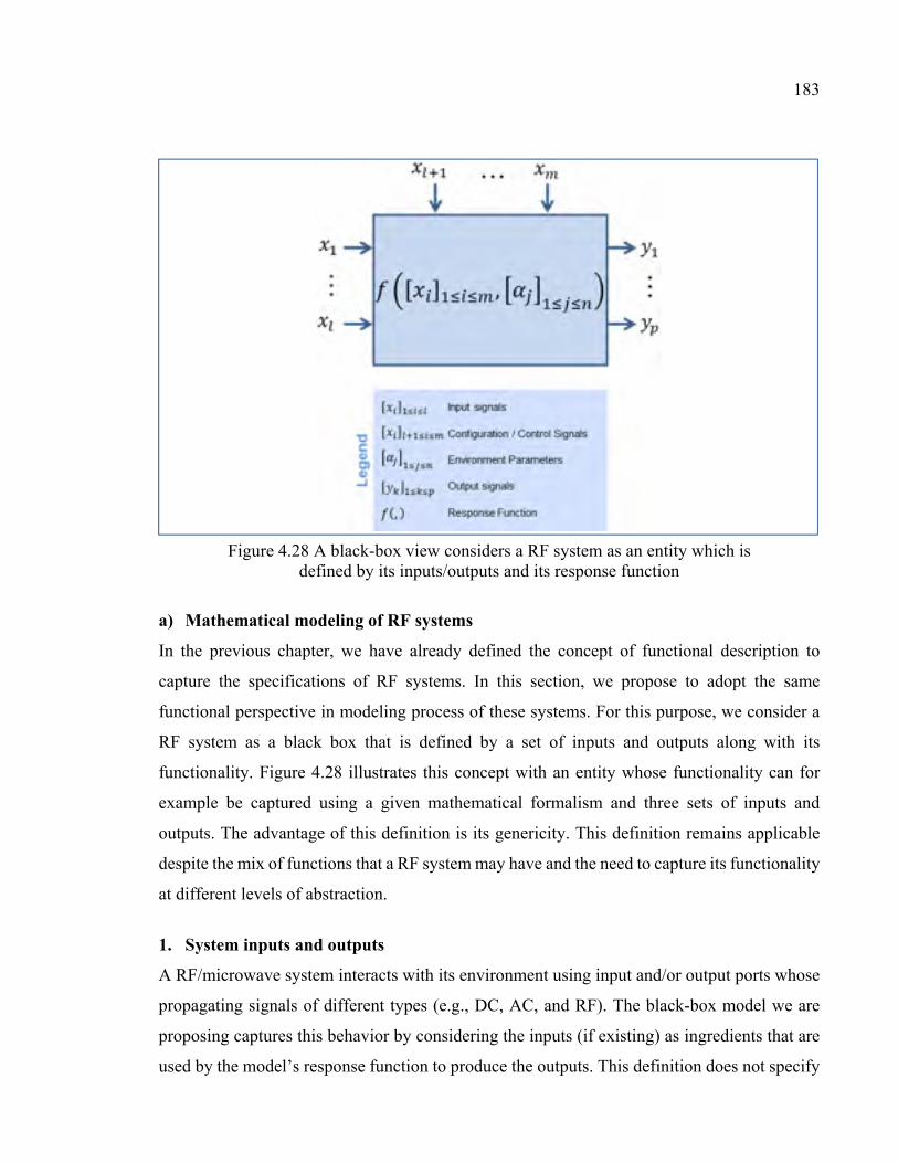
183
Figure 4.28 A black-box view considers a RF system as an entity which is defined by its inputs/outputs and its response function
a) Mathematical modeling of RF systems
In the previous chapter, we have already defined the concept of functional description to
capture the specifications of RF systems. In this section, we propose to adopt the same
functional perspective in modeling process of these systems. For this purpose, we consider a
RF system as a black box that is defined by a set of inputs and outputs along with its
functionality. Figure 4.28 illustrates this concept with an entity whose functionality can for
example be captured using a given mathematical formalism and three sets of inputs and
outputs. The advantage of this definition is its genericity. This definition remains applicable
despite the mix of functions that a RF system may have and the need to capture its functionality
at different levels of abstraction.
1. System inputs and outputs
A RF/microwave system interacts with its environment using input and/or output ports whose
propagating signals of different types (e.g., DC, AC, and RF). The black-box model we are
proposing captures this behavior by considering the inputs (if existing) as ingredients that are
used by the model’s response function to produce the outputs. This definition does not specify
184
in prior the directionality of ports which allows to describe situations were inputs and outputs
may interchange their roles during system’s operation. At this regard, we define two types of
inputs:
− Regular inputs: (designated by and in Table 4.2) represent a typical AC or RF
signal, and
− Control inputs: (designated by _ in Table 4.2) represent a signal (typically DC) that is
used to drive the RF/microwave system (e.g., input voltage in a voltage-controlled
oscillator and an automatic-gain control);
− Environment parameters: (designated by in Figure 4.28) represent variables that are not
regular signal inputs to the system but characterize the environment and the context of
operation (e.g. time, temperature, frequency, reference impedance, etc.).
This said, it might be sometimes useful, from abstraction perspective, to ignore some inputs
(respectively outputs) in the modeling of some RF systems. In this case, there is generally a
“hidden” input (respectively output) that is not considered in the model. For instance, biasing
input voltages may be ignored in oscillators and amplifiers. The reflected RF signal is generally
neglected in a termination device. These cases are represented in Table 4.2 by a void symbol
(∅).
As shown in Figure 4.28, the model’s response function takes as input two vectors of and
elements (i.e., signal and environment inputs respectively) and produces a vector of elements
(i.e., outputs). The examples of Table 4.2 suggest that input and output signals (i.e., , _
and ) are assumed to be single voltage or power magnitudes. This is true for this case. But
in general, a regular input (respectively output ) can be a list of parameters characterizing
different measurements and/or constants related to a given port (e.g., power, frequency,
impedance, etc.) and this is regardless of environment inputs. In this case, (respectively
output ) is represented as ( , , , … ) (respectively ( , , , … )).
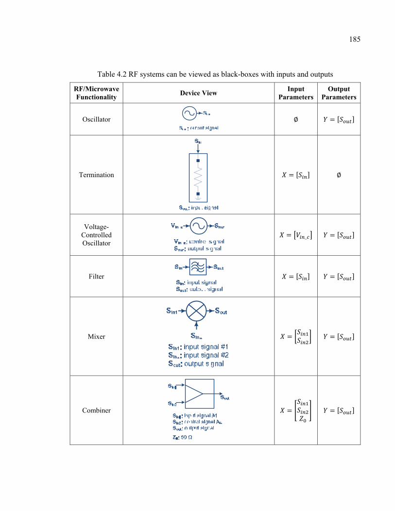
185
Table 4.2 RF systems can be viewed as black-boxes with inputs and outputs
RF/Microwave Functionality
Device View Input
Parameters Output
Parameters
Oscillator
∅ = [ ]
Termination
= [ ] ∅
Voltage-Controlled Oscillator
= _ = [ ] Filter
= [ ] = [ ]
Mixer
= = [ ]
Combiner
= = [ ]
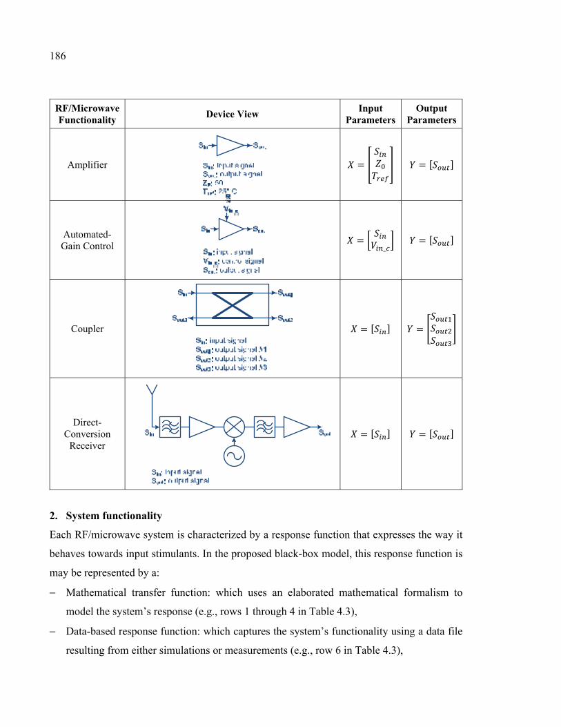
186
RF/Microwave Functionality
Device View Input
Parameters Output
Parameters
Amplifier
= = [ ] Automated-Gain Control
= _ = [ ]
Coupler
= [ ] =
Direct-Conversion
Receiver = [ ] = [ ]
2. System functionality
Each RF/microwave system is characterized by a response function that expresses the way it
behaves towards input stimulants. In the proposed black-box model, this response function is
may be represented by a:
− Mathematical transfer function: which uses an elaborated mathematical formalism to
model the system’s response (e.g., rows 1 through 4 in Table 4.3),
− Data-based response function: which captures the system’s functionality using a data file
resulting from either simulations or measurements (e.g., row 6 in Table 4.3),
187
− Expression-based response function: which uses mathematical equations along with
datasets to characterize the system’s functionality (e.g., rows 5 in Table 4.3), and
− Hybrid response function: that uses a mix of the previous types to characterize the system’s
functionality.
In the first four rows of Table 4.3, “first-order” mathematical functions (i.e., equations (4.1)
through (4.4)) where defined to model the frequency response of four RF building blocks (i.e.,
Class-A amplifier, bandpass filter, mixer and oscillator). These examples of response functions
are intended only to illustrate how a system’s functionality can be mathematically described.
In fact, the mathematical modeling of RF systems is more complex than what is presented in
these trivial examples. For instance, it should characterize the device’s response in different
operation scenarios (e.g., large vs. small signal) and domains (e.g., frequency vs. time domain).
The last two rows of Table 4.3 present the response function of a switch and a typical linear
file-based component. The first one is defined by a table that gives the switch states every 10
milliseconds (i.e., switching speed). The second is captured using a Touchstone file (i.e.,
scattering parameters). It is worth noting that the response function is not unique. Therefore, a
RF system can be modeled for example using two response functions: one is mathematical and
the other is file-based. It is for instance the case of a bandpass RF filter which is also a linear
device. Then, its response function can be either as given in equation (4.2) or as presented in
row 6 of Table 4.3. This said, the major advantage of all these response function representations
is their independence from technology that makes them good candidates for high-level
abstraction in RF domain.
b) Formal modeling of RF systems
Since the black-box model allows to capturing individual RF system in terms of functionality
and inputs/outputs (i.e., interfaces), we need to extend the usability of this definition in order
to: (i) describe complex systems (i.e., composed of multiple parts and building blocks) and (ii)
capture the different aspects pertaining to the composition, the interaction and the attributes of
these complex systems as well as the various relationships that may exist between them.
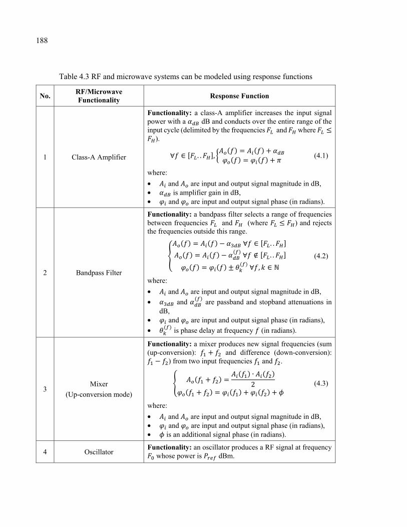
188
Table 4.3 RF and microwave systems can be modeled using response functions
No. RF/Microwave Functionality
Response Function
1 Class-A Amplifier
Functionality: a class-A amplifier increases the input signal power with a dB and conducts over the entire range of the input cycle (delimited by the frequencies and where ≤
). ∀ ∈ [ . . ], ( ) = ( ) +( ) = ( ) + (4.1)
where:
• and are input and output signal magnitude in dB, • is amplifier gain in dB, • and are input and output signal phase (in radians).
2 Bandpass Filter
Functionality: a bandpass filter selects a range of frequencies between frequencies and (where ≤ ) and rejects the frequencies outside this range. ( ) = ( ) − ∀ ∈ [ . . ]( ) = ( ) − ( ) ∀ ∉ [ . . ]( ) = ( ) ± ( ) ∀ , ∈ ℕ (4.2)
where:
• and are input and output signal magnitude in dB,
• and ( ) are passband and stopband attenuations in dB,
• and are input and output signal phase (in radians),
• ( ) is phase delay at frequency (in radians).
3 Mixer
(Up-conversion mode)
Functionality: a mixer produces new signal frequencies (sum (up-conversion): + and difference (down-conversion): − ) from two input frequencies and . ( + ) = ( ) ∙ ( )2( + ) = ( ) + ( ) + (4.3)
where:
• and are input and output signal magnitude in dB, • and are input and output signal phase (in radians), • is an additional signal phase (in radians).
4 Oscillator Functionality: an oscillator produces a RF signal at frequency
whose power is dBm.
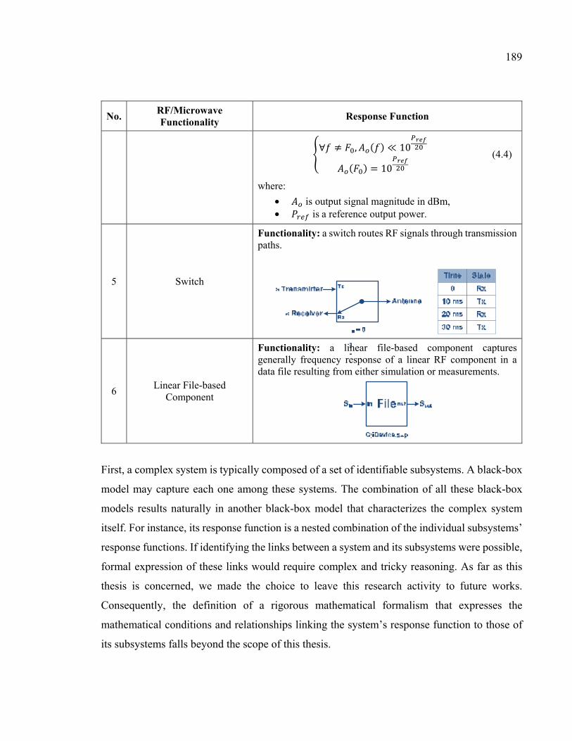
189
No. RF/Microwave Functionality
Response Function
∀ ≠ , ( ) ≪ 10( ) = 10 (4.4)
where:
• is output signal magnitude in dBm, • is a reference output power.
5 Switch
Functionality: a switch routes RF signals through transmission paths.
6 Linear File-based
Component
Functionality: a linear file-based component captures generally frequency response of a linear RF component in a data file resulting from either simulation or measurements.
First, a complex system is typically composed of a set of identifiable subsystems. A black-box
model may capture each one among these systems. The combination of all these black-box
models results naturally in another black-box model that characterizes the complex system
itself. For instance, its response function is a nested combination of the individual subsystems’
response functions. If identifying the links between a system and its subsystems were possible,
formal expression of these links would require complex and tricky reasoning. As far as this
thesis is concerned, we made the choice to leave this research activity to future works.
Consequently, the definition of a rigorous mathematical formalism that expresses the
mathematical conditions and relationships linking the system’s response function to those of
its subsystems falls beyond the scope of this thesis.

190
Moreover, the black-box model was proposed mainly to simplify as much as possible the
representation of a RF system. That is why all the details related to the internal building blocks
(e.g., composition, organization, interactions, etc.) were removed. Thus, this model is capable
to describe an individual or a set of interrelated RF systems in terms of response function and
inputs/outputs. Nevertheless, it delivers little information about how these subsystems are
organized (i.e., structure) and interact (i.e., behavior). To capture these aspects, a mechanism
of strong semantics is required. We have already faced this issue in the previous chapter when
we had to define mechanisms for functional description of RF systems. The solution we have
proposed is the use of a modeling language (i.e., SysML84) in order to express not only the
design structural and behavioral aspects but also capturing its requirements and specifications.
Therefore, we will make use again of modeling languages in order to “formally” express the
requirements, structural and behavioral aspects of RF systems. It is worth to note that the word
“formal” used in this context does not denote rigorous mathematical construction but rather
compliance with semantic rules and constraints of a given modeling language.
Regarding SysML, it dedicates three main types of diagrams for the structural description of a
system:
− Block definition diagram (bdd): it is used for the description of system’s components and
hierarchy,
− Internal definition diagram (ibd): it is used for the depiction of internal structure of the
system and its components, and
− Package diagram (pkg): it gathers system models in logical collections whose describing a
given view of the system.
SysML dedicates four additional types of diagrams for the description of system’s dynamic
behavior:
− Activity diagram (act): it is used to captures the evolution of the system in terms of
activities,
84 The reader may refer to APPENDIX II (p. 439) for more detailed overview of SysML.
191
− Sequence diagram (sd): it describes the flow of messages and interactions between the
different system components,
− State machine diagram (stm): it describe the system status at each state and its transitions
between two different states, and
− Use case diagram (uc): it captures how external actors use the system and how it is expected
to react towards external actions.
In addition, SysML has introduced two new diagrams to help designers expressing domain-
specific artefacts:
− Requirements diagram (req): it is used for the definition of constraints and rules (including
mathematical formulas, physical laws, mechanical constraints, etc.) that are associated to
the system properties of to those related to its building blocks. Thus, it helps integrating
system models with relevant engineering tools to carry out various system analyses and
simulations (e.g., performance, reliability, etc.), and
− Parametric diagram (par): it provides modeling constructs to capture text-based
requirements into graphical, tabular or tree structure format and associate them with the
system’s structural and/or behavioral model elements using predefined relationships.
The structure of a black-box model of a RF system (as depicted in Figure 4.28) can be captured
using a block definition diagram (bdd) as shown in Figure 4.29. The system is described by a
block, namely RF system, whose environment parameters are captured in the section “values”
and its response function is captured in the section “constraints”. This block is composed of
blocks, namely input ports (respectively blocks, namely output ports). The environment
parameters related to each port can be captured in the section “values”.
In general, real-world RF systems (e.g. receivers, transmitters, etc.) are not described as single
blocks. Designers need to architect the internals of such systems at different levels of
granularity (depending on the adopted topology) and from different design perspectives (e.g.
electrical, mechanical, thermal, etc.). Then, is it possible to use SysML to capture the internal
architecture and behavior of such complex systems?
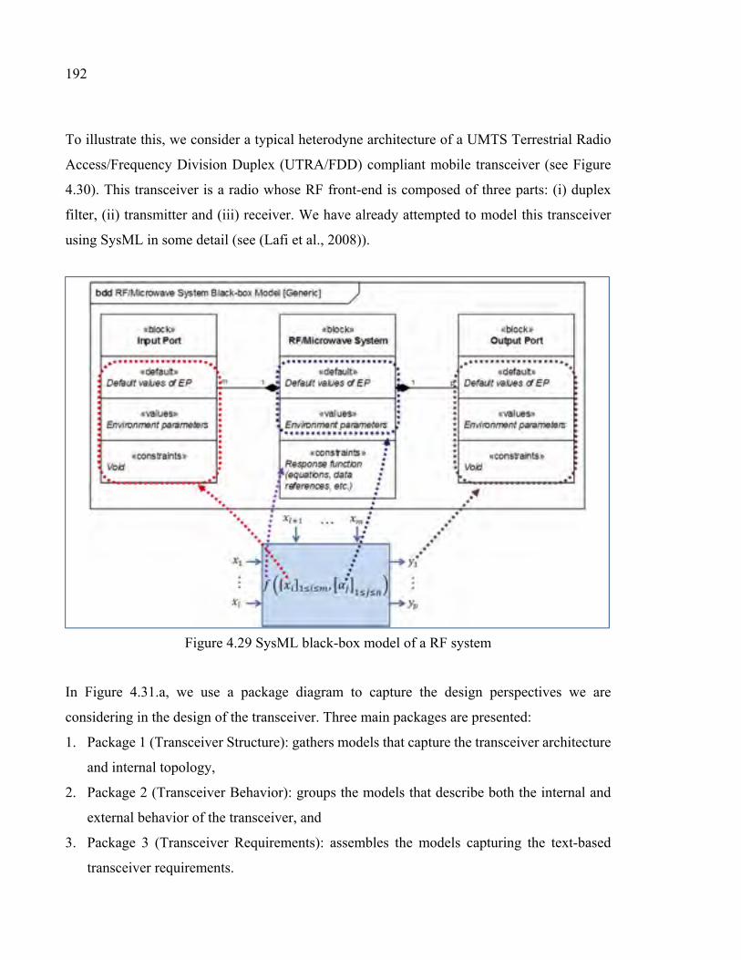
192
To illustrate this, we consider a typical heterodyne architecture of a UMTS Terrestrial Radio
Access/Frequency Division Duplex (UTRA/FDD) compliant mobile transceiver (see Figure
4.30). This transceiver is a radio whose RF front-end is composed of three parts: (i) duplex
filter, (ii) transmitter and (iii) receiver. We have already attempted to model this transceiver
using SysML in some detail (see (Lafi et al., 2008)).
Figure 4.29 SysML black-box model of a RF system
In Figure 4.31.a, we use a package diagram to capture the design perspectives we are
considering in the design of the transceiver. Three main packages are presented:
1. Package 1 (Transceiver Structure): gathers models that capture the transceiver architecture
and internal topology,
2. Package 2 (Transceiver Behavior): groups the models that describe both the internal and
external behavior of the transceiver, and
3. Package 3 (Transceiver Requirements): assembles the models capturing the text-based
transceiver requirements.
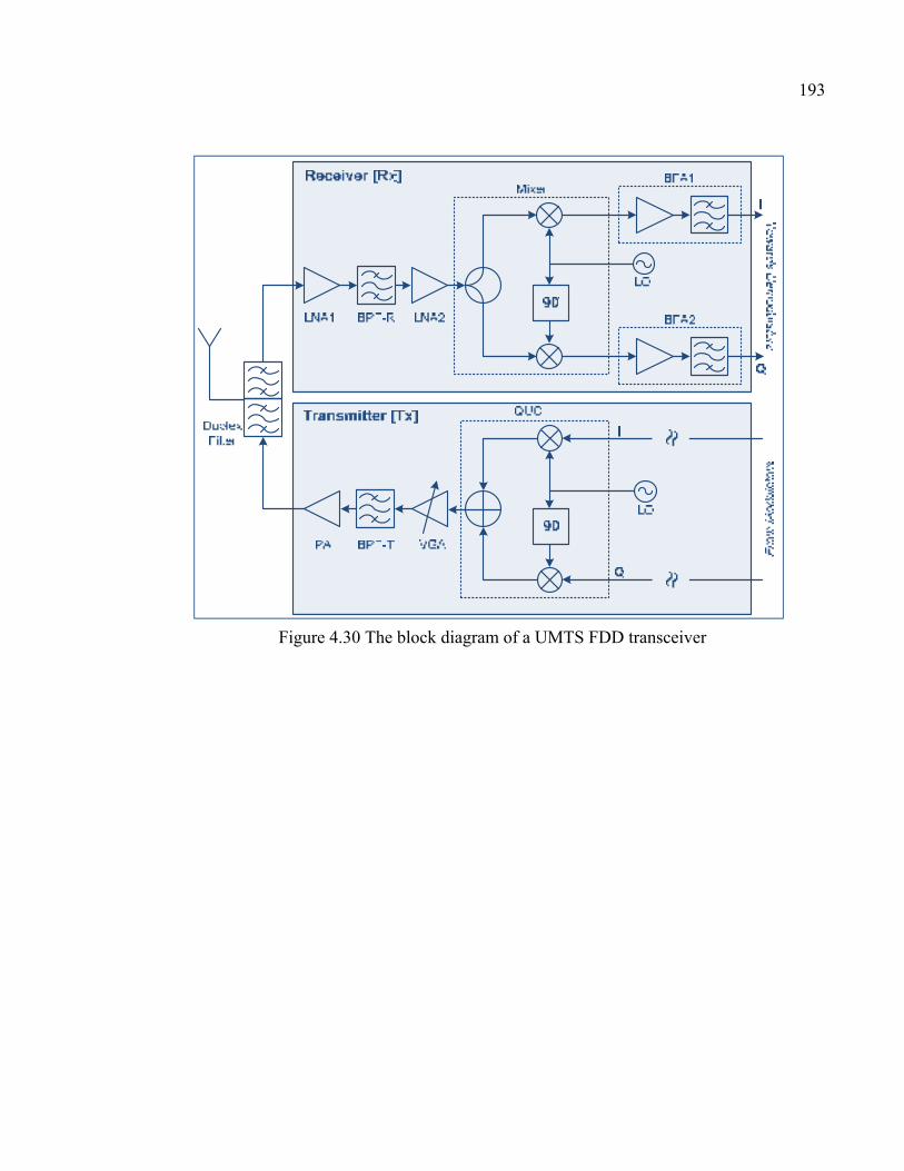
193
Figure 4.30 The block diagram of a UMTS FDD transceiver
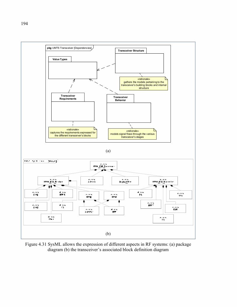
194
pkg UMTS Transceiver [Dependencies]
Value Types
Transceiver Requirements
Transceiver Structure
Transceiver Behavior
«rationale»captures the requirements expressed for
the different transceiver’s blocks
«rationale»models signal flows through the various
transceiver’s stages
«rationale»gathers the models pertaining to the
transceiver’s building blocks and internal structure
(a)
(b)
Figure 4.31 SysML allows the expression of different aspects in RF systems: (a) package diagram (b) the transceiver’s associated block definition diagram
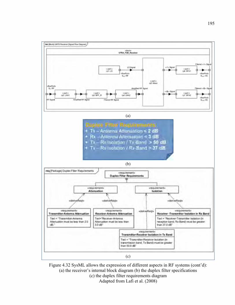
195
(a)
(b)
(c)
Figure 4.32 SysML allows the expression of different aspects in RF systems (cont’d): (a) the receiver’s internal block diagram (b) the duplex filter specifications
(c) the duplex filter requirements diagram Adapted from Lafi et al. (2008)
196
All three packages are associated to a fourth package, namely “values types” (using a
“dependency” relationship). In this package, we capture the measurements units (e.g.,
[Frequency, MHz], [Chip rate, Mcps], [bit rate, Kbps], etc.) and dimensions that characterize
the signals and flows travelling through the different transceiver blocks and parts. The package
diagram of Figure 4.31.a shows the highest abstraction level we have considered in (Lafi et al.,
2008).
The block definition diagram (bdd) of Figure 4.31.b and the internal block definition diagram
of Figure 4.32.a are among of the models contained in package 1. The former depicts the
internal hierarchy of the transceiver while the latter shows the flow of signals within the
receiver. In addition, Figure 4.32.b depicts a piece from the written specifications of the duplex
filter composing the UMTS transceiver. We used a requirement diagram to capture these
specifications (as presented Figure 4.32.c). It is always possible to associate these requirements
to the structure and behavior models in which the duplex filter is depicted either for the purpose
of design verification and validation or for improving traceability. In this case, the models we
have developed are only for illustrative purposes and small enough to be easily understood.
4.3.4 Abstraction Levels, Viewpoints and Views
In the previous section, we elaborated a general model for a RF system that is a black box
described only by its functionality and its input/output parameters. We also established that
this assumption remains applicable when considering a RF system as a combination of other
RF “sub-”systems whose functionalities and inputs/outputs are fully identifiable. Then, we
learned how to use a modeling language (i.e., SysML) to capture, particularly the black-box
model associated to a RF system as well as the common design aspects (i.e., structure, behavior
and requirements) of a complex system.
In this section, we address three main abstraction issues pertaining to common design aspects
of a RF system:
1. Which abstraction levels can be considered for the description of RF systems? and how are
they tied each to others?
197
2. How a RF/microwave system can be described from different design perspectives (i.e.,
viewpoints)?
3. Which modeling views can be derived to describe a RF system from each design
perspective (i.e., viewpoint)?
a) Abstraction Levels
The UMTS transceiver of Figure 4.30 is a RF system that can be subdivided into three main
subsystems: (i) transmitter, (ii) receiver and (iii) duplex filter. The transmitter and the receiver
are also RF systems that can be subdivided into a number of building blocks (e.g., amplifier,
quadrature up-converter, filter, etc.) while the duplex filter can be derived into a network of
electrical elements. Each building block of the transmitter (respectively the receiver) is similar
to the duplex filter in a sense that it can also be derived into a network of electrical elements.
In general, each of these elements is conceptually represented by an electrical component (e.g.,
transistor, diode, lumped component, distributed line, etc.) that is intended to perform a basic
(i.e., low-level) functionality. This conceptual representation was meant to abstract the
physical structure required to accomplish that functionality. Three observations may be
concluded from the analysis of this example:
1. It is possible to subdivide a given RF system into groupings that characterize not only an
identifiable functionality but also a level of complexity,
2. The number of these groupings is limited because each one of them corresponds to a unique
aspect of the RF system, and
3. If the level of complexity changes from different neutral standpoints while the functionality
and the inputs/outputs remain the same, it is not possible to define a new grouping because
only the granularity of the original grouping is changing.
Generalizing these observations to all RF systems may be successful if (i) a grouping is defined
as an “abstraction level” and (ii) the aspects to be considered are design-dependent. From the
RF designer’s point of view, a RF system can be considered as a physical implementation, a
conceptual circuit, a modular topology, and an architecture of individual functionalities. For
each design perspective, the number of elements composing the RF system may differ
depending on how the designer subdivides it for the purpose of a solution. This characteristic,
198
related to the number of elements in a RF system at a given abstraction level, is called
“granularity”. The change of granularity level alters the solution domain (i.e., how the solution
is constructed) but does not impact the abstraction level. Considering these assumptions, we
can define four distinct abstraction levels in RF systems (see Figure 4.33):
1. Atomic Layer: On the contrary to digital design where the lowest abstraction level (i.e.,
physical) is represented by a “device” (i.e., typically a silicon-based transistor),
RF/microwave systems physical implementation cannot be represented by a single device
due to the predominant mix of technologies85. For this reason, we consider the lowest
abstraction level in RF system (that is conceptually representing the physical design
perspective) as a “layer” of atomic components. The term “layer” denotes that many
individual devices may represent the physical design perspective of RF systems. The term
“atomic” indicates that each component of this layer cannot be subdivided further from RF
design perspective. Otherwise, it can no longer be subdivided into elements that might be
captured using a black-box model. For instance, we have identified four groups of atomic
components that can be considered as parts of the atomic layer: transmission lines, lumped
components, nonlinear devices and sources (see examples in Table 4.4 and Figure 4.34).
Obviously, if a RF system is represented as a tree hierarchy, these atomic components lie
down at the “leaf” level;
2. Circuit: Traditionally, atomic components are assembled to build a physical
implementation. This assembly can also be regarded from the electrical viewpoint. If so,
the physical details are ignored while the electrical properties are emphasized. This new
design perspective defines a higher level of abstraction, namely “circuit”. A circuit is
simply a network composed of electrical elements that are connected by a media through
which electrical signals flow (e.g., current, wave). At the circuit level, it is obvious that the
atomic components loose virtually their physical properties. They become represented by
electrical functions (that may be described for example by mathematical formulas) as well
as their respective input/output flows (e.g., current, voltage, etc.);
85 The topic of technology predominance in RF systems and its impact on design was thoroughly detailed in section 1.4 of chapter 1 and section 2.3.3 of chapter 2.
199
3. Module: One or many circuits can be assembled in a given topology to construct a self-
contained entity. The design perspective is no longer electrical but structural. The
corresponding abstraction level is “module”. This entity can be defined as an individual,
independent and interchangeable unit that can be used to build more complex structures.
At this level of abstraction, the internal electrical properties of a module are hidden. It is
defined by its functionality and inputs/outputs;
4. System: As interchangeable units, modules can be used to construct complex structures.
From this design viewpoint, the internal structure of each module is not the primary
concern of the designer who focuses more on how to organize the modules to achieve a
specified functionality regardless of how the internals of each module were structured.
Thus, the design perspective is more architectural/functional rather than structural. This
new abstraction level, namely “system”, is all about arranging individual subsystems (i.e.,
modules) into an architecture that accomplishes a predefined functionality. A system is
trivially an assembly of interconnected modules to form a complex and unitary whole
achieving a given functionality.
The four abstraction levels are arranged as shown in Figure 4.33. The atomic layer (i.e.,
composed of atomic components) is the lowest abstraction level. The circuit level lies on the
top of the atomic layer while the module level lies between the former and the system level.
This makes the system is the highest abstraction level. When moving up from a lower to higher
abstraction level, this is called “abstraction”. Inversely, moving down from a higher to a lower
abstraction level is “refinement”.
Since a RF system can be regarded from different viewpoints, it is always possible to change
the abstraction level. The action of lowering or raising the abstraction level implies:
1. An increase or a decrease in the level of detail (i.e., complexity),
2. A change in the design perspective (i.e., viewpoint), and
3. The nature of at least one among the functionality and the inputs/outputs changes.
In general, the number of atomic components is limited (i.e., countable) because it depends on
the available technologies. However, it is virtually possible to build an infinite number of
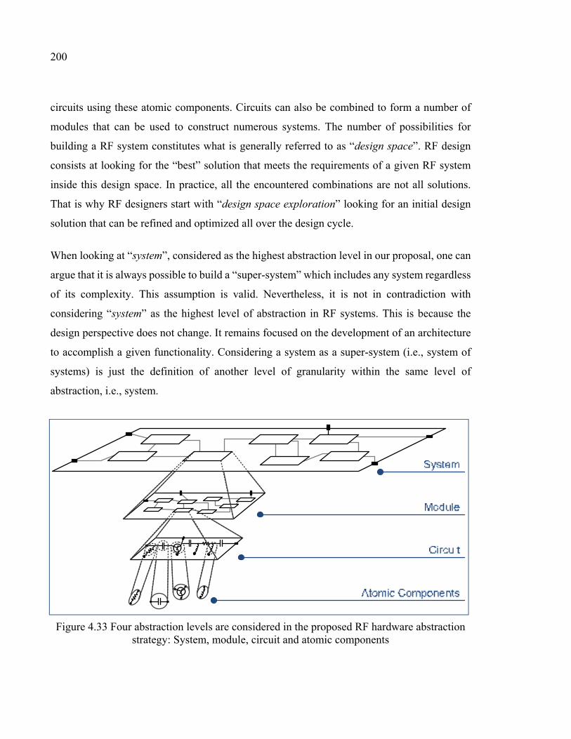
200
circuits using these atomic components. Circuits can also be combined to form a number of
modules that can be used to construct numerous systems. The number of possibilities for
building a RF system constitutes what is generally referred to as “design space”. RF design
consists at looking for the “best” solution that meets the requirements of a given RF system
inside this design space. In practice, all the encountered combinations are not all solutions.
That is why RF designers start with “design space exploration” looking for an initial design
solution that can be refined and optimized all over the design cycle.
When looking at “system”, considered as the highest abstraction level in our proposal, one can
argue that it is always possible to build a “super-system” which includes any system regardless
of its complexity. This assumption is valid. Nevertheless, it is not in contradiction with
considering “system” as the highest level of abstraction in RF systems. This is because the
design perspective does not change. It remains focused on the development of an architecture
to accomplish a given functionality. Considering a system as a super-system (i.e., system of
systems) is just the definition of another level of granularity within the same level of
abstraction, i.e., system.
Figure 4.33 Four abstraction levels are considered in the proposed RF hardware abstraction
strategy: System, module, circuit and atomic components
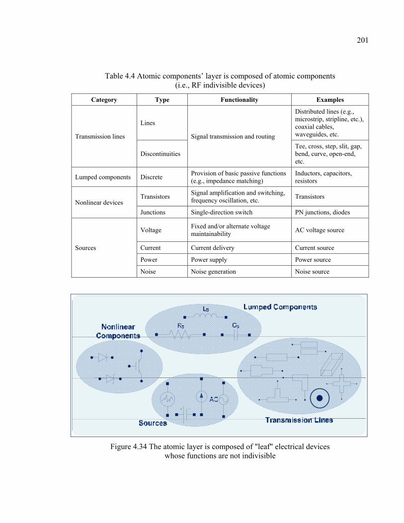
201
Table 4.4 Atomic components’ layer is composed of atomic components (i.e., RF indivisible devices)
Category Type Functionality Examples
Transmission lines
Lines
Signal transmission and routing
Distributed lines (e.g., microstrip, stripline, etc.), coaxial cables, waveguides, etc.
Discontinuities Tee, cross, step, slit, gap, bend, curve, open-end, etc.
Lumped components Discrete Provision of basic passive functions (e.g., impedance matching)
Inductors, capacitors, resistors
Nonlinear devices Transistors
Signal amplification and switching, frequency oscillation, etc.
Transistors
Junctions Single-direction switch PN junctions, diodes
Sources
Voltage Fixed and/or alternate voltage maintainability
AC voltage source
Current Current delivery Current source
Power Power supply Power source
Noise Noise generation Noise source
Figure 4.34 The atomic layer is composed of "leaf" electrical devices whose functions are not indivisible
202
In summary, the four abstraction levels (i.e., atomic layer, circuit, module and system)
proposed in this section are meant to describe the level of complexity of a RF system from a
given design perspective (i.e., viewpoint). For illustration, Figure 4.35 shows a typical
architecture of a direct-conversion receiver RF front-end. At system level, the receiver is
perceived as a unitary whole. It receives all radio spectrum signals and outputs a specific signal
that corresponds to one or many radio channels. At module level, the level of complexity
increases. It can be decomposed for example into seven individual building blocks (i.e.,
modules). Each one of these building blocks is in charge of a given functionality. For example,
the antenna receives the RF signals and routes them to the filter which selects the desired radio
channel(s). The resulting output signal is amplified using a low-noise amplifier (LNA). The
amplified signal is then merged with the signal produced by the local oscillator using the mixer.
The following filter selects the down-converted signal and removes its up-converted
counterpart as well as the subsequent intermodulation products. Finally, an amplifier amplifies
the resulting signal before it is delivered to the demodulator (i.e., in digital stage). At circuit
level, each building block is described by an electrical circuit. For example, the LNA may be
derived into a typical Class-C amplifier while the oscillator is implemented using a Colpitts86
architecture. It is obvious that the complexity at this abstraction level is greater than the upper
one. At the lowest abstraction level (i.e., atomic-component layer), the individual components
which are abstracted in each circuit by their electrical parameters (including their schematic)
are handled at the physical level. For instance, a PNP transistor is not represented at this level
by its electrical schematic but rather its physical layout (i.e., composed of different metal and
insulator layers).
b) Abstraction Viewpoints
An effective way to design a complex system is to separately focus on a particular set of similar
aspects within that system at each design step. This is the concept of separation of concerns.
86 Colpitts oscillator was invented by Edwin H. Colpitts in 1918. It uses a combination of inductors and capacitors to form a feedback loop to the active device (i.e., typically a transistor). The oscillation frequency
is determined by = || .
203
For example, the designer focuses only on tuning the electrical parameters of an amplifier
circuit before figuring out which physical dimensions the transistors should have to get the
same frequency response. Focusing on the electrical and the physical aspects separately gives
better results than searching a design space considering both electrical and physical parameters
at the same time. The concept of separation of concerns is an abstraction mechanism that
defines clear, separate and complementary design perspectives. Each of them embodies from
the designer’s point of view (i.e., viewpoint), a specific set of issues to address within the
system in order to figure out a potential solution. A design perspective corresponds to a
designer viewpoint. A viewpoint is a neutral observation position of a RF system where only
particular design concerns are highlighted. In simple words, an abstraction viewpoint is like a
camera that films the system from a specific direction. As shown in Figure 4.36, several aspects
can be emphasized in a typical RF system. For example, it can be described as black box where
the functionally is defined by a set of user-defined requirements. It can also be observed as a
circuit where only the electrical properties are underlined. In addition, it can be viewed as a
physical structure where its intrinsic physical attributes are highlighted.
In this thesis, we consider five abstraction viewpoints from which RF systems can be observed
and described:
1. Physical: from this viewpoint, the system is described exclusively by its physical attributes.
For example, a simple device such as a transistor is described by its dimensions (e.g.,
length, width), the number of layers as well as the type of materials and substrates used for
its implementation, etc. When a whole system is involved, other physical information may
be added to this description (e.g., the system’s layout, devices placement, devices wiring
and signals routing, etc.);
2. Electrical: the system is regarded from this point of view as a circuit that is exclusively
specified by its electrical characteristics. For instance, a device (e.g., resistor) is defined by
the electrical voltage between its ends, the current flowing through it and its characteristic
impedance. In addition to devices electrical characteristics, a system is specified by a
circuit that allows the application of electrical laws (e.g., Kirchhoff law, superposition law,
etc.). This implies the existence of a connectivity plan (e.g., netlist) that defines how
devices are wired as well as reference nodes (e.g., ground, sources, loads, etc.);

204
3. Structural: from this viewpoint, the designer’s interest is neither physical nor electrical.
The focus is on how to arrange basic parts (e.g., circuits, devices, etc.) in order to build a
system’s topology. These parts may or may not be self-contained and interchangeable. For
example, a phase-locked loop is structured from this point of view as control system where
phase detectors, filters, dividers, voltage-controlled oscillators and other parts are arranged
in the main and the loop paths. It is worth noting that the structural viewpoint is not purely
mechanical, as the term may suggest, but denotes especially system assembly and
integration aspects;
4. Architectural: from this viewpoint, the designer is interested in how a system is structured
using self-contained and interchangeable parts. This viewpoint expresses generally a
contractual architecture that is predefined by the high-level specifications. For example, a
radio system (e.g., receiver) may be architected in compliance to a given reference
architecture (e.g., homodyne, super-heterodyne, etc.). In some cases, this viewpoint is not
considered because the system’s complexity is reduced in a way that the structural
viewpoint is enough to characterize its structure;
5. Functional: this viewpoint is mostly interested in the system’s functionality and operation.
It aims to define the purpose of a RF system and how it is expected to work. Thus, it defines
for example its operation constraints as well as the specific role of each actor or building
part within that system (if a given reference architecture is already contracted).
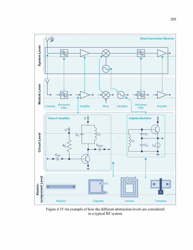
205
Sys
tem
Le
vel
Amplifier AmplifierOscillatorMixerBandpass
FilterAntenna
Mo
du
le L
eve
l
Bandpass Filter
Cir
cuit
Lev
elA
tom
ic-
com
po
nen
t L
evel
Direct-Conversion Receiver
Colpitts-OscillatorClass-C Amplifier
Resistor Capacitor TransistorInductor
...L||C||
R|| CSout
CSin
V+
V-
L||
C1
C2 IC
...
Figure 4.35 An example of how the different abstraction levels are considered in a typical RF system
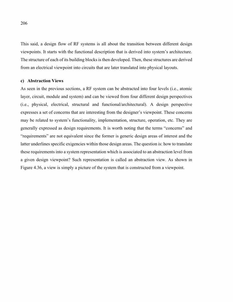
206
This said, a design flow of RF systems is all about the transition between different design
viewpoints. It starts with the functional description that is derived into system’s architecture.
The structure of each of its building blocks is then developed. Then, these structures are derived
from an electrical viewpoint into circuits that are later translated into physical layouts.
c) Abstraction Views
As seen in the previous sections, a RF system can be abstracted into four levels (i.e., atomic
layer, circuit, module and system) and can be viewed from four different design perspectives
(i.e., physical, electrical, structural and functional/architectural). A design perspective
expresses a set of concerns that are interesting from the designer’s viewpoint. These concerns
may be related to system’s functionality, implementation, structure, operation, etc. They are
generally expressed as design requirements. It is worth noting that the terms “concerns” and
“requirements” are not equivalent since the former is generic design areas of interest and the
latter underlines specific exigencies within those design areas. The question is: how to translate
these requirements into a system representation which is associated to an abstraction level from
a given design viewpoint? Such representation is called an abstraction view. As shown in
Figure 4.36, a view is simply a picture of the system that is constructed from a viewpoint.
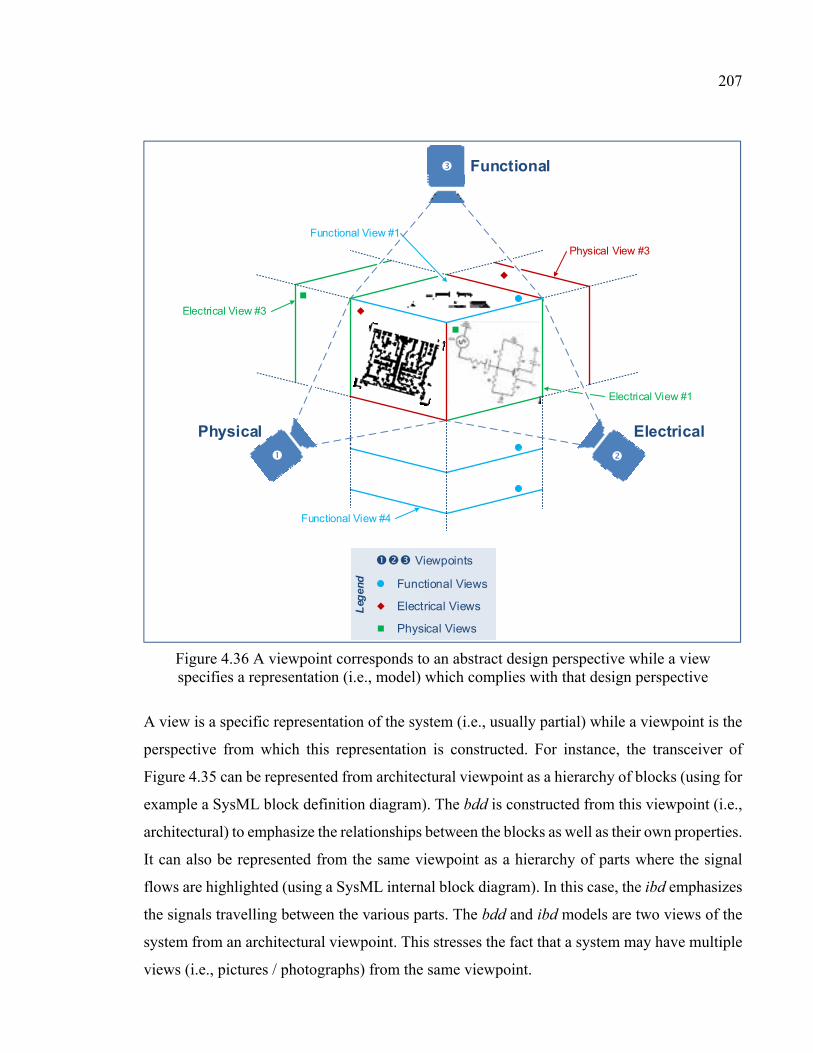
207
Lege
nd
Electrical
Viewpoints
Physical
Functional
Functional View #4
Functional Views
Electrical Views
Physical Views
Functional View #1
Electrical View #3
Physical View #3
Electrical View #1
Figure 4.36 A viewpoint corresponds to an abstract design perspective while a view specifies a representation (i.e., model) which complies with that design perspective
A view is a specific representation of the system (i.e., usually partial) while a viewpoint is the
perspective from which this representation is constructed. For instance, the transceiver of
Figure 4.35 can be represented from architectural viewpoint as a hierarchy of blocks (using for
example a SysML block definition diagram). The bdd is constructed from this viewpoint (i.e.,
architectural) to emphasize the relationships between the blocks as well as their own properties.
It can also be represented from the same viewpoint as a hierarchy of parts where the signal
flows are highlighted (using a SysML internal block diagram). In this case, the ibd emphasizes
the signals travelling between the various parts. The bdd and ibd models are two views of the
system from an architectural viewpoint. This stresses the fact that a system may have multiple
views (i.e., pictures / photographs) from the same viewpoint.
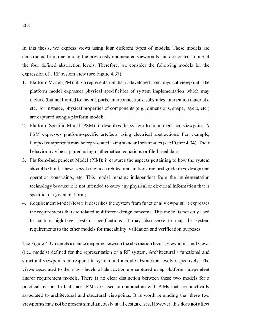
208
In this thesis, we express views using four different types of models. These models are
constructed from one among the previously-enumerated viewpoints and associated to one of
the four defined abstraction levels. Therefore, we consider the following models for the
expression of a RF system view (see Figure 4.37):
1. Platform Model (PM): it is a representation that is developed from physical viewpoint. The
platform model expresses physical specificities of system implementation which may
include (but not limited to) layout, ports, interconnections, substrates, fabrication materials,
etc. For instance, physical properties of components (e.g., dimensions, shape, layers, etc.)
are captured using a platform model;
2. Platform-Specific Model (PSM): it describes the system from an electrical viewpoint. A
PSM expresses platform-specific artefacts using electrical abstractions. For example,
lumped components may be represented using standard schematics (see Figure 4.34). Their
behavior may be captured using mathematical equations or file-based data;
3. Platform-Independent Model (PIM): it captures the aspects pertaining to how the system
should be built. These aspects include architectural and/or structural guidelines, design and
operation constraints, etc. This model remains independent from the implementation
technology because it is not intended to carry any physical or electrical information that is
specific to a given platform;
4. Requirement Model (RM): it describes the system from functional viewpoint. It expresses
the requirements that are related to different design concerns. This model is not only used
to capture high-level system specifications. It may also serve to map the system
requirements to the other models for traceability, validation and verification purposes.
The Figure 4.37 depicts a coarse mapping between the abstraction levels, viewpoints and views
(i.e., models) defined for the representation of a RF system. Architectural / functional and
structural viewpoints correspond to system and module abstraction levels respectively. The
views associated to these two levels of abstraction are captured using platform-independent
and/or requirement models. There is no clear distinction between these two models for a
practical reason. In fact, most RMs are used in conjunction with PIMs that are practically
associated to architectural and structural viewpoints. It is worth reminding that these two
viewpoints may not be present simultaneously in all design cases. However, this does not affect
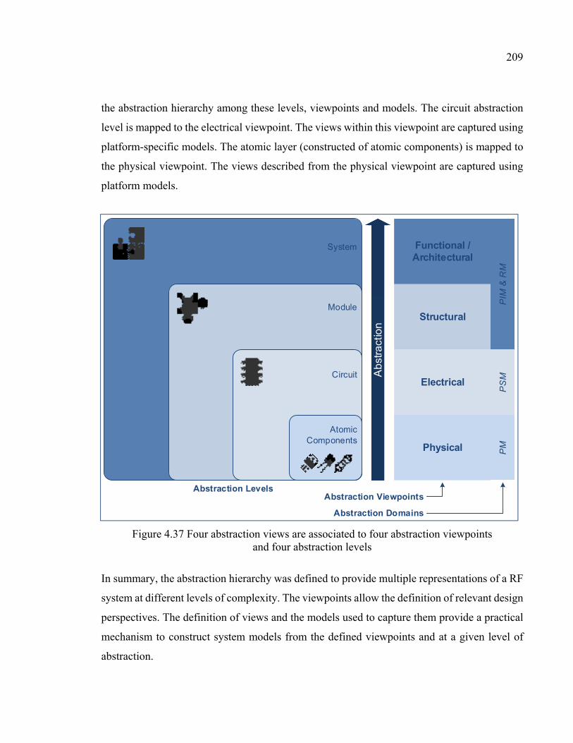
209
the abstraction hierarchy among these levels, viewpoints and models. The circuit abstraction
level is mapped to the electrical viewpoint. The views within this viewpoint are captured using
platform-specific models. The atomic layer (constructed of atomic components) is mapped to
the physical viewpoint. The views described from the physical viewpoint are captured using
platform models.
Ab
stra
ctio
n
Physical
Electrical
Structural
Functional / Architectural
PM
PS
MP
IM &
RM
Abstraction LevelsAbstraction Viewpoints
Abstraction Domains
System
Module
Circuit
AtomicComponents
Figure 4.37 Four abstraction views are associated to four abstraction viewpoints and four abstraction levels
In summary, the abstraction hierarchy was defined to provide multiple representations of a RF
system at different levels of complexity. The viewpoints allow the definition of relevant design
perspectives. The definition of views and the models used to capture them provide a practical
mechanism to construct system models from the defined viewpoints and at a given level of
abstraction.
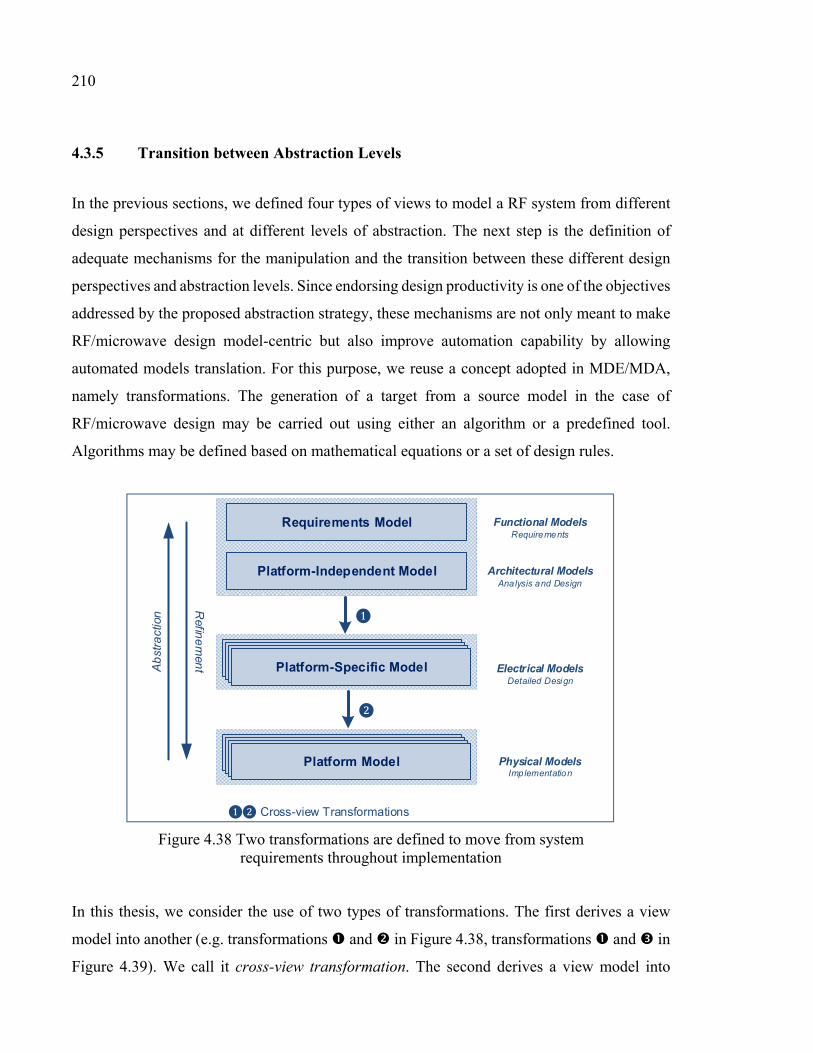
210
4.3.5 Transition between Abstraction Levels
In the previous sections, we defined four types of views to model a RF system from different
design perspectives and at different levels of abstraction. The next step is the definition of
adequate mechanisms for the manipulation and the transition between these different design
perspectives and abstraction levels. Since endorsing design productivity is one of the objectives
addressed by the proposed abstraction strategy, these mechanisms are not only meant to make
RF/microwave design model-centric but also improve automation capability by allowing
automated models translation. For this purpose, we reuse a concept adopted in MDE/MDA,
namely transformations. The generation of a target from a source model in the case of
RF/microwave design may be carried out using either an algorithm or a predefined tool.
Algorithms may be defined based on mathematical equations or a set of design rules.
Functional Models
Platform Model
Platform-Specific Model
Platform-Independent Model
Requirements Model
Ab
stra
ctio
n
Refin
em
ent
❶❷ Cross-view Transformations
Architectural Models
Electrical Models
Physical Models
❶
❷
Analysis and Design
Detailed Design
Implementation
Requirements
Figure 4.38 Two transformations are defined to move from system requirements throughout implementation
In this thesis, we consider the use of two types of transformations. The first derives a view
model into another (e.g. transformations and in Figure 4.38, transformations and in
Figure 4.39). We call it cross-view transformation. The second derives a view model into
211
another of the same type (e.g., transformations and in Figure 4.39). We name it intra-
view transformation.
a) Cross-view transformations
A cross-view transformation converts a view model (i.e., RM, PIM, PSM and PM) to another.
It is similar to model-to-model transformations adopted in MDE/MDA. In the following, we
will use only two cross-view transformations. The first translates RMs and/or PIM into one or
many PSMs. The second translates a PSM into one or many platform models. For simplicity,
we will not consider a transformation that translates a requirements model into a platform-
independent model despite the fact that the former is defined at a higher level of abstraction
than the latter. The main reason behind this is purely practical: as it will be discussed in the
next sections, we use requirement models in RF/microwave design as part of the functional
description process, which is completed by the definition of a PIM (i.e., often manually
constructed). The main interest behind the RMs is particularly addressing the concerns of
specifications capture and visualization, validation and verification as well as traceability
within the RF/microwave design cycle. Consequently, there is a close relationship between
RMs and PIM, which makes the construction of both models, interrelated. This said, it is
always possible (theoretically speaking) to consider a transformation that converts a RM to a
PIM.
To distinguish the cross-view transformations shown in Figure 4.38, we consider:
1. The high-level cross-view transformation (no. )
It derives functional and/or architectural models into one or many electrical models. The
former models are expressed using SysML diagrams and semantics. The latter are represented
using electrical schematics and abstractions. This transformation generates platform-specific
information from functional and architectural artefacts without specifying any physical
information about the target platform. In Figure 4.39, the requirements model (i.e., Req SysML
diagram) captures some requirements pertaining to an attenuator while the PIM defines that
attenuator’s structure and properties (using a SysML bdd diagram). The transformation (no.
) converts these models into two electrical models (represented using two circuits). The first
212
implements a T-pad attenuator circuit while the second implements a π-pad. In both cases, the
platform-specific information includes the circuits’ topologies and the values of the resistive
elements used within these circuits. A typical transformation to derive the T-pad (respectively
π-pad) attenuator network may be based on the algorithm and mathematical formalism
presented in Table 4.5. In addition to the possibility of deriving multiple PSMs for multiple
platforms, this example shows that a transformation can also derive more than one PSM for
the same platform;
2. The low-level cross-view transformation (no. )
It generates one or many physical models from the electrical ones. The physical models may
be captured using a ready-to-manufacture layout. This transformation uses technology input
pertaining to the target platform in order to derive the physical models. It acts into steps: (i)
technology mapping that consists of associating each PSM element with the relevant
technology information, and (ii) physical model generation which derives the corresponding
implementation (e.g., layout). As depicted in Figure 3.12, technology input may include
substrate and material characteristics, real lumped-component realizations, etc. In the example
of Figure 4.39, the T-pad (respectively π-pad) attenuator physical model is represented by its
subsequent layout. The layout shows the resistive discrete elements (i.e., thin-film resistors)
which are linked using distributed transmission lines. The transformation of the electrical to
physical models may be carried out using appropriate tools. For example, a commercial design
package such ADS may be used to derive the PSMs of Figure 4.39 into layouts.
In addition, a cross-view transformation may be reversible. In this case, it is composed of two
sub-transformations: one is direct which converts model A into model B, and the other is
reverse which performs the opposite conversion. Reversible transformations are difficult to
develop because they require a rigorous mapping between the artefacts of both source and
target models. However, automated reversible transformations are powerful because they
allow fast design re-spins.
213
b) Intra-view transformations
The second type of transformations converts a model to another model of the same kind. This
means that both the source and target models share the same level of abstraction and are
developed from the same abstraction viewpoint. Then, it is possible to convert a functional
(respectively architectural, structural, electrical and physical) model to another one. For
example, a T-pad attenuator PSM can be converted into a π-pad attenuator PSM (see
transformation in Figure 4.39). A T-pad attenuator PM can be converted to a π-pad
attenuator platform model (see transformation in Figure 4.39).
Depending on the granularity level within the considered abstraction view, intra-view
transformations may be classified into two main categories: (i) view-model bridges and (ii)
granularity refinement transformations. The former transforms a source to a target model
without changing the granularity level of the original one while the latter one does. Before
presenting these two categories of transformations, we first review the concept of granularity
refinement (already presented in section 3.3.3 of chapter 3) in the light of the proposed
abstraction strategy.
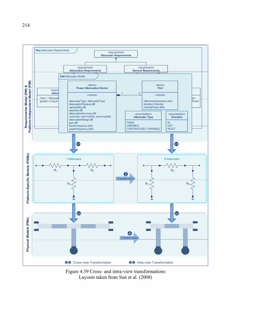
214
Req Attenuator Requirements
«requirement»Attenuator Requirements
Text=”Attenuation covers a bandwidth between lowerFrequency and upperFrequency”
«requirement»Bandwidth
«requirement»Attenuation Requirements
«requirement»General Requirements
«deriveReqt»
Text = “Attenuation must be greater or equal to abs(gain) dB.”
«requirement»Attenuation
«deriveReqt»
Text = “Reference impedance at each port must be equal to referenceImpedance ohms”
«requirement»Reference Impedance
«deriveReqt»
Text = “Maximum operating power at each port must be greater or equal to maxOpPower dBm”
«requirement»Operating Power
«deriveReqt»
Pla
tfo
rm-S
pec
ific
Mo
de
ls (
PS
Ms
)
Π Attenuator
R1 R3
R2
T Attenuator
R2
R1 R3
Req
uir
em
en
ts M
od
el (
RM
) &
Pla
tfo
rm-I
nd
epen
de
nt
Mo
de
l (P
IM)
Ph
ysic
al M
od
els
(P
Ms
)
Transform
ation
Transform
ation
Transformation
Transformation
Transform
ation
Transform
ation
bdd Attenuator Model
«block»Power Attenuation Device
«values»
attenuatorType: AttenuatorTypeattenuationFlatness:dBrepeatibility:dBstepSize:dBattenuationAccuracy:dB«interval» min=minAtt, max=maxAtt attenuationRange:dBgain:dBlowerFrequency:GHzupperFrequency:GHz
«block»Port
«values»
referenceImpedance:ohmdirection:DirectionmaxOpPower:dBm
1 2
«enumeration»Attenuator Type
FIXEDVARIABLECONTINUOUSLY VARIABLE
«enumeration»Direction
INOUTINOUT
Cross-view Transformation Intra-view Transformation
Figure 4.39 Cross- and intra-view transformations Layouts taken from Sun et al. (2008)
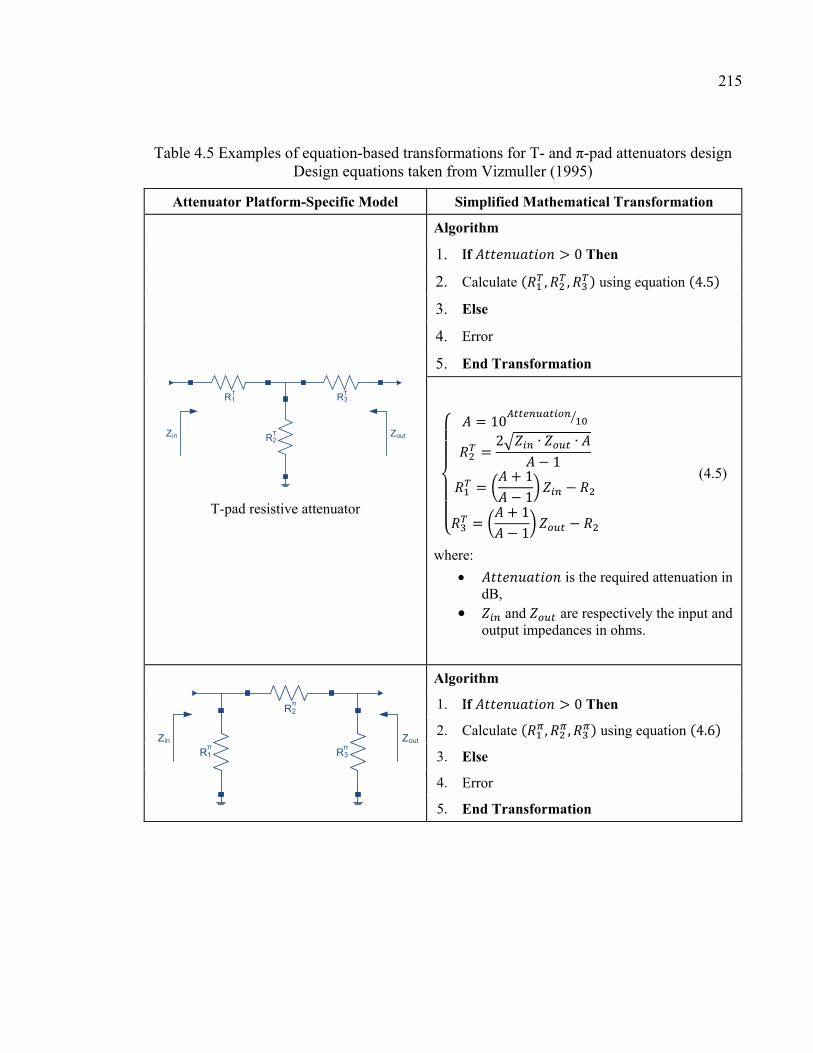
215
Table 4.5 Examples of equation-based transformations for T- and π-pad attenuators design Design equations taken from Vizmuller (1995)
Attenuator Platform-Specific Model Simplified Mathematical Transformation
R2
R1 R3
ZoutZin
T
T
T
T-pad resistive attenuator
Algorithm
1. If > 0 Then
2. Calculate ( , , ) using equation (4.5) 3. Else
4. Error
5. End Transformation
= 10= 2 ∙ ∙− 1= + 1− 1 −= + 1− 1 − (4.5)
where:
• is the required attenuation in dB,
• and are respectively the input and output impedances in ohms.
R1 R3
R2
Zin Zoutπ
π
π
Algorithm
1. If > 0 Then
2. Calculate ( , , ) using equation (4.6) 3. Else
4. Error
5. End Transformation
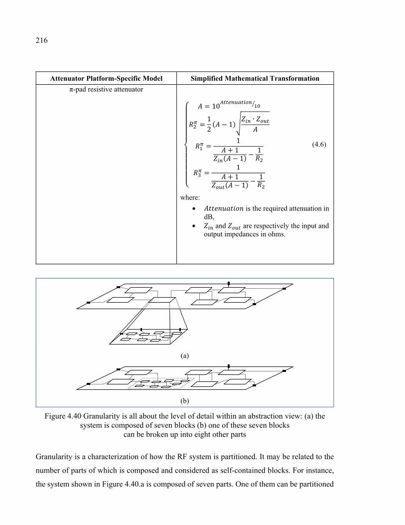
216
Attenuator Platform-Specific Model Simplified Mathematical Transformation
π-pad resistive attenuator = 10= 12 ( − 1) ∙= 1+ 1( − 1) − 1= 1+ 1( − 1) − 1
(4.6)
where:
• is the required attenuation in dB,
• and are respectively the input and output impedances in ohms.
(a)
(b)
Figure 4.40 Granularity is all about the level of detail within an abstraction view: (a) the system is composed of seven blocks (b) one of these seven blocks
can be broken up into eight other parts
Granularity is a characterization of how the RF system is partitioned. It may be related to the
number of parts of which is composed and considered as self-contained blocks. For instance,
the system shown in Figure 4.40.a is composed of seven parts. One of them can be partitioned
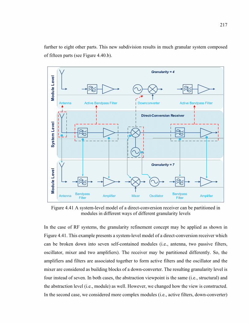
217
further to eight other parts. This new subdivision results in much granular system composed
of fifteen parts (see Figure 4.40.b).
Sys
tem
Le
vel
Amplifier AmplifierOscillatorMixerBandpass
FilterAntenna
Mo
du
le L
eve
l
Bandpass Filter
Direct-Conversion Receiver
DownconverterActive Bandpass FilterAntenna Active Bandpass Filter
Mo
du
le L
eve
l
Granularity = 7
Granularity = 4
Figure 4.41 A system-level model of a direct-conversion receiver can be partitioned in modules in different ways of different granularity levels
In the case of RF systems, the granularity refinement concept may be applied as shown in
Figure 4.41. This example presents a system-level model of a direct-conversion receiver which
can be broken down into seven self-contained modules (i.e., antenna, two passive filters,
oscillator, mixer and two amplifiers). The receiver may be partitioned differently. So, the
amplifiers and filters are associated together to form active filters and the oscillator and the
mixer are considered as building blocks of a down-converter. The resulting granularity level is
four instead of seven. In both cases, the abstraction viewpoint is the same (i.e., structural) and
the abstraction level (i.e., module) as well. However, we changed how the view is constructed.
In the second case, we considered more complex modules (i.e., active filters, down-converter)
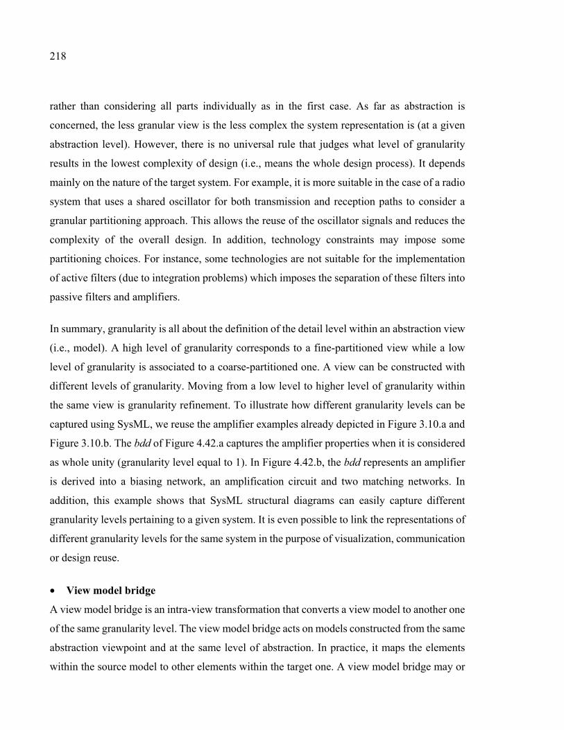
218
rather than considering all parts individually as in the first case. As far as abstraction is
concerned, the less granular view is the less complex the system representation is (at a given
abstraction level). However, there is no universal rule that judges what level of granularity
results in the lowest complexity of design (i.e., means the whole design process). It depends
mainly on the nature of the target system. For example, it is more suitable in the case of a radio
system that uses a shared oscillator for both transmission and reception paths to consider a
granular partitioning approach. This allows the reuse of the oscillator signals and reduces the
complexity of the overall design. In addition, technology constraints may impose some
partitioning choices. For instance, some technologies are not suitable for the implementation
of active filters (due to integration problems) which imposes the separation of these filters into
passive filters and amplifiers.
In summary, granularity is all about the definition of the detail level within an abstraction view
(i.e., model). A high level of granularity corresponds to a fine-partitioned view while a low
level of granularity is associated to a coarse-partitioned one. A view can be constructed with
different levels of granularity. Moving from a low level to higher level of granularity within
the same view is granularity refinement. To illustrate how different granularity levels can be
captured using SysML, we reuse the amplifier examples already depicted in Figure 3.10.a and
Figure 3.10.b. The bdd of Figure 4.42.a captures the amplifier properties when it is considered
as whole unity (granularity level equal to 1). In Figure 4.42.b, the bdd represents an amplifier
is derived into a biasing network, an amplification circuit and two matching networks. In
addition, this example shows that SysML structural diagrams can easily capture different
granularity levels pertaining to a given system. It is even possible to link the representations of
different granularity levels for the same system in the purpose of visualization, communication
or design reuse.
• View model bridge
A view model bridge is an intra-view transformation that converts a view model to another one
of the same granularity level. The view model bridge acts on models constructed from the same
abstraction viewpoint and at the same level of abstraction. In practice, it maps the elements
within the source model to other elements within the target one. A view model bridge may or
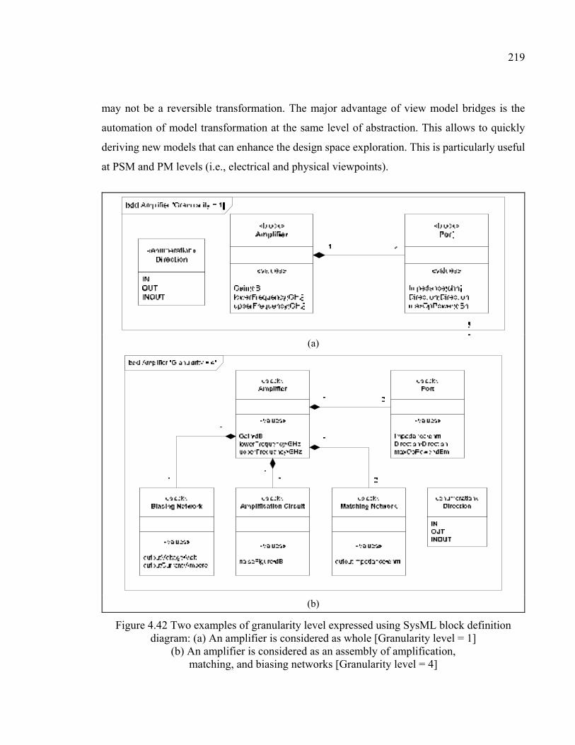
219
may not be a reversible transformation. The major advantage of view model bridges is the
automation of model transformation at the same level of abstraction. This allows to quickly
deriving new models that can enhance the design space exploration. This is particularly useful
at PSM and PM levels (i.e., electrical and physical viewpoints).
(a)
(b)
Figure 4.42 Two examples of granularity level expressed using SysML block definition diagram: (a) An amplifier is considered as whole [Granularity level = 1]
(b) An amplifier is considered as an assembly of amplification, matching, and biasing networks [Granularity level = 4]
220
PSM bridge
Π Attenuator
R1 R3
R2
T Attenuator
R2
R1 R3
π
π
π
TT
T
Figure 4.43 Reversible platform-specific model for resistive attenuators
In RF design, this concept is particularly useful when PIM, PSM and PM models are involved.
For example, an attenuator PSM implemented using a T-pad network may be converted to an
equivalent π-pad network using a PSM bridge (as illustrated in Figure 4.43). This PSM bridge
makes an association between the resistive elements of T- and π-pad networks respectively.
The elements of the latter may be derived from those of the former using the equation (4.7).
Inversely, the elements of the T-pad network may be derived from those of π-pad network
using the equation (4.8). The combination of these two equations results in a reversible PSM
bridge that can be used to transform a T-pad to π-pad resistive attenuator network and vice-
versa.
= + += + += + + (4.7)
= + += + += + + (4.8)
221
• Granularity refinement transformation
Granularity refinement transformation converts a source view model into another one of
different granularity level. By opposition to model bridges, this type of transformations does
not necessarily map each element in the source model to another one in the target model.
However, an element within the source model (respectively the target model) might be mapped
to one or many elements within the target model (respectively source model). To illustrate this
concept, a traditional unbalanced T-pad attenuator network may be converted into a balanced
one as shown in Figure 4.44.a. In this case, the source model has a granularity level equal to
three while the target model has a granularity level equal to five. The input and output resistors
in the unbalanced attenuator were respectively derived into two resistors elements in the
balanced attenuator. Similarly, a balanced π-pad attenuator may be derived from an unbalanced
configuration. The granularity level changes from three in the latter to four in the former (see
Figure 4.44.b). Based on the equations (4.9) and (4.10), relevant granularity refinement
transformations can be implemented to derive both balanced T- and π-pad attenuator circuits
from unbalanced structures.
= = 2== = 2 (4.9)
== = 2= (4.10)
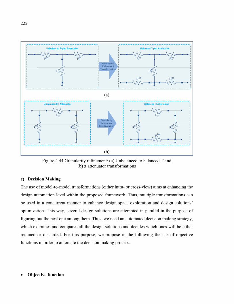
222
UT
UT UT
Unbalanced T-pad Attenuator
R2
R1 R3
Granularity Refinement
Transformation
Balanced T-pad Attenuator
R2
R1 R3
BT
BT BT
R4 R5BT BT
(a)
Unbalanced Π Attenuator
R1 R3
R2
Uπ
Uπ
Uπ
Balanced Π Attenuator
R1 R3
R2
Bπ
Bπ
Bπ
R4Bπ
Granularity Refinement
Transformation
(b)
Figure 4.44 Granularity refinement: (a) Unbalanced to balanced T and (b) π attenuator transformations
c) Decision Making
The use of model-to-model transformations (either intra- or cross-view) aims at enhancing the
design automation level within the proposed framework. Thus, multiple transformations can
be used in a concurrent manner to enhance design space exploration and design solutions’
optimization. This way, several design solutions are attempted in parallel in the purpose of
figuring out the best one among them. Thus, we need an automated decision making strategy,
which examines and compares all the design solutions and decides which ones will be either
retained or discarded. For this purpose, we propose in the following the use of objective
functions in order to automate the decision making process.
• Objective function
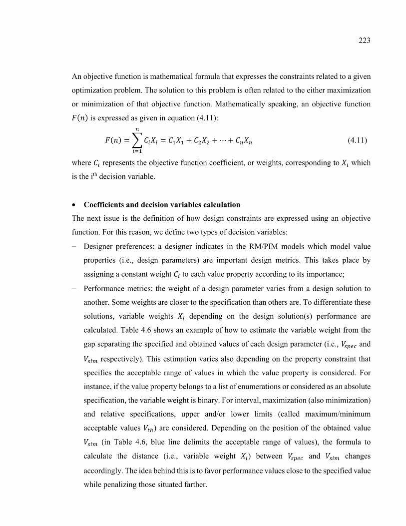
223
An objective function is mathematical formula that expresses the constraints related to a given
optimization problem. The solution to this problem is often related to the either maximization
or minimization of that objective function. Mathematically speaking, an objective function ( ) is expressed as given in equation (4.11):
( ) = = + +⋯+ (4.11)
where represents the objective function coefficient, or weights, corresponding to which
is the ith decision variable.
• Coefficients and decision variables calculation
The next issue is the definition of how design constraints are expressed using an objective
function. For this reason, we define two types of decision variables:
− Designer preferences: a designer indicates in the RM/PIM models which model value
properties (i.e., design parameters) are important design metrics. This takes place by
assigning a constant weight to each value property according to its importance;
− Performance metrics: the weight of a design parameter varies from a design solution to
another. Some weights are closer to the specification than others are. To differentiate these
solutions, variable weights depending on the design solution(s) performance are
calculated. Table 4.6 shows an example of how to estimate the variable weight from the
gap separating the specified and obtained values of each design parameter (i.e., and
respectively). This estimation varies also depending on the property constraint that
specifies the acceptable range of values in which the value property is considered. For
instance, if the value property belongs to a list of enumerations or considered as an absolute
specification, the variable weight is binary. For interval, maximization (also minimization)
and relative specifications, upper and/or lower limits (called maximum/minimum
acceptable values ) are considered. Depending on the position of the obtained value
(in Table 4.6, blue line delimits the acceptable range of values), the formula to
calculate the distance (i.e., variable weight ) between and changes
accordingly. The idea behind this is to favor performance values close to the specified value
while penalizing those situated farther.
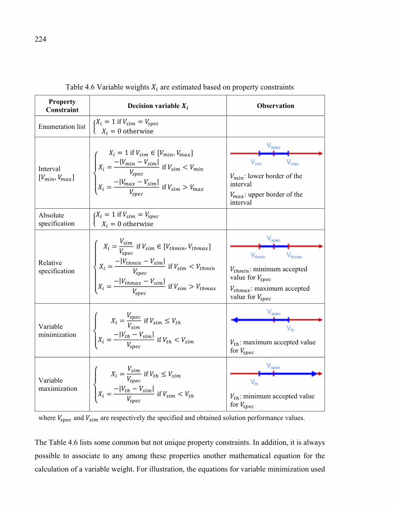
224
Table 4.6 Variable weights are estimated based on property constraints
Property Constraint
Decision variable Observation
Enumeration list = 1if == 0otherwise
Interval [ , ] = 1if ∈ [ , ]= −| − | if <
= −| − | if > : lower border of the interval
: upper border of the interval
Absolute specification
= 1if == 0otherwise
Relative specification
= if ∈ [ , ]= −| − | if <= −| − | if > : minimum accepted
value for
: maximum accepted value for
Variable minimization
= if ≤= −| − | if <
: maximum accepted value for
Variable maximization
= if ≤= −| − | if <
: minimum accepted value for
where and are respectively the specified and obtained solution performance values.
The Table 4.6 lists some common but not unique property constraints. In addition, it is always
possible to associate to any among these properties another mathematical equation for the
calculation of a variable weight. For illustration, the equations for variable minimization used
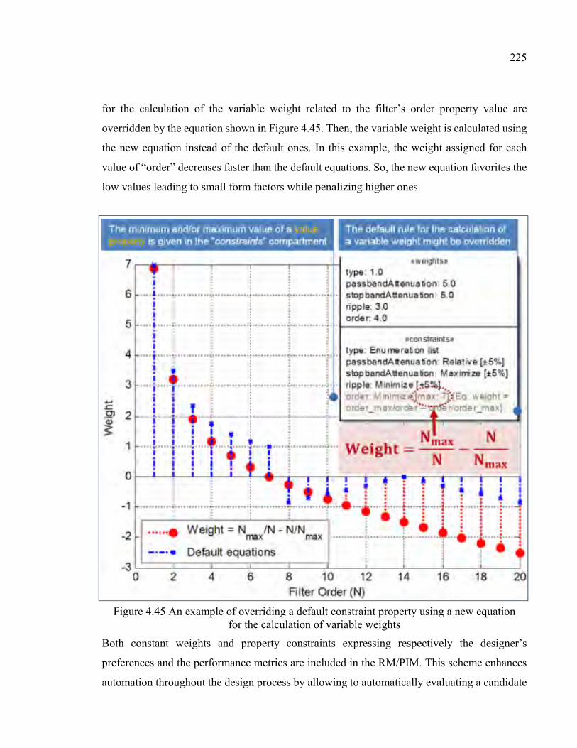
225
for the calculation of the variable weight related to the filter’s order property value are
overridden by the equation shown in Figure 4.45. Then, the variable weight is calculated using
the new equation instead of the default ones. In this example, the weight assigned for each
value of “order” decreases faster than the default equations. So, the new equation favorites the
low values leading to small form factors while penalizing higher ones.
Figure 4.45 An example of overriding a default constraint property using a new equation for the calculation of variable weights
Both constant weights and property constraints expressing respectively the designer’s
preferences and the performance metrics are included in the RM/PIM. This scheme enhances
automation throughout the design process by allowing to automatically evaluating a candidate
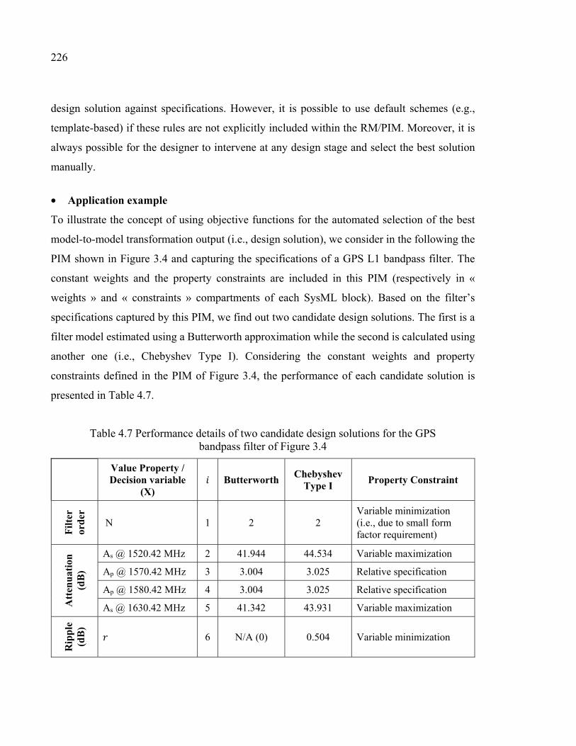
226
design solution against specifications. However, it is possible to use default schemes (e.g.,
template-based) if these rules are not explicitly included within the RM/PIM. Moreover, it is
always possible for the designer to intervene at any design stage and select the best solution
manually.
• Application example
To illustrate the concept of using objective functions for the automated selection of the best
model-to-model transformation output (i.e., design solution), we consider in the following the
PIM shown in Figure 3.4 and capturing the specifications of a GPS L1 bandpass filter. The
constant weights and the property constraints are included in this PIM (respectively in «
weights » and « constraints » compartments of each SysML block). Based on the filter’s
specifications captured by this PIM, we find out two candidate design solutions. The first is a
filter model estimated using a Butterworth approximation while the second is calculated using
another one (i.e., Chebyshev Type I). Considering the constant weights and property
constraints defined in the PIM of Figure 3.4, the performance of each candidate solution is
presented in Table 4.7.
Table 4.7 Performance details of two candidate design solutions for the GPS bandpass filter of Figure 3.4
Value Property / Decision variable
(X) Butterworth
Chebyshev Type I
Property Constraint
Fil
ter
ord
er
N 1 2 2 Variable minimization (i.e., due to small form factor requirement)
Att
enu
atio
n
(dB
)
As @ 1520.42 MHz 2 41.944 44.534 Variable maximization
Ap @ 1570.42 MHz 3 3.004 3.025 Relative specification
Ap @ 1580.42 MHz 4 3.004 3.025 Relative specification
As @ 1630.42 MHz 5 41.342 43.931 Variable maximization
Rip
ple
(d
B)
6 N/A (0) 0.504 Variable minimization
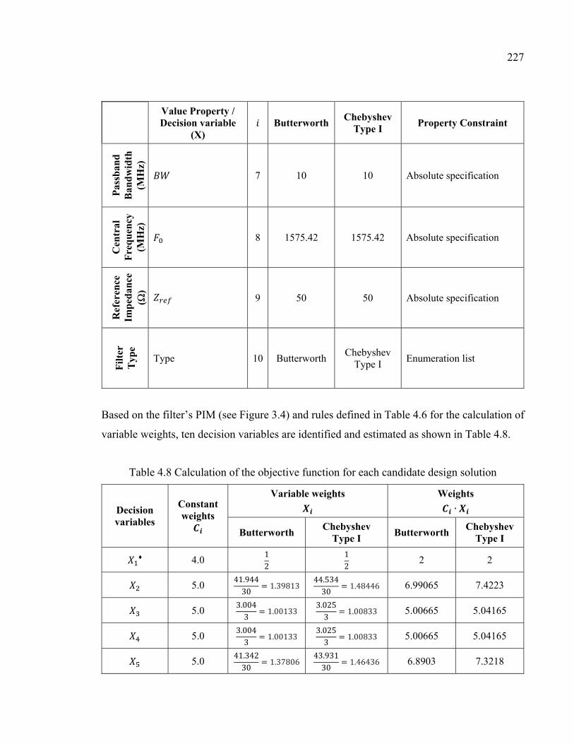
227
Value Property / Decision variable
(X) Butterworth
Chebyshev Type I
Property Constraint P
assb
and
B
and
wid
th
(MH
z)
7 10 10 Absolute specification
Cen
tral
F
req
uen
cy
(MH
z)
8 1575.42 1575.42 Absolute specification
Ref
eren
ce
Imp
edan
ce
(Ω)
9 50 50 Absolute specification
Fil
ter
Typ
e
Type 10 Butterworth Chebyshev
Type I Enumeration list
Based on the filter’s PIM (see Figure 3.4) and rules defined in Table 4.6 for the calculation of
variable weights, ten decision variables are identified and estimated as shown in Table 4.8.
Table 4.8 Calculation of the objective function for each candidate design solution
Decision variables
Constant weights
Variable weights
Weights ∙
Butterworth Chebyshev
Type I Butterworth
Chebyshev Type I
♦ 4.0 12
12 2 2
5.0 41.94430 = 1.39813
44.53430 = 1.48446 6.99065 7.4223
5.0 3.0043 = 1.00133
3.0253 = 1.00833 5.00665 5.04165
5.0 3.0043 = 1.00133
3.0253 = 1.00833 5.00665 5.04165
5.0 41.34230 = 1.37806
43.93130 = 1.46436 6.8903 7.3218
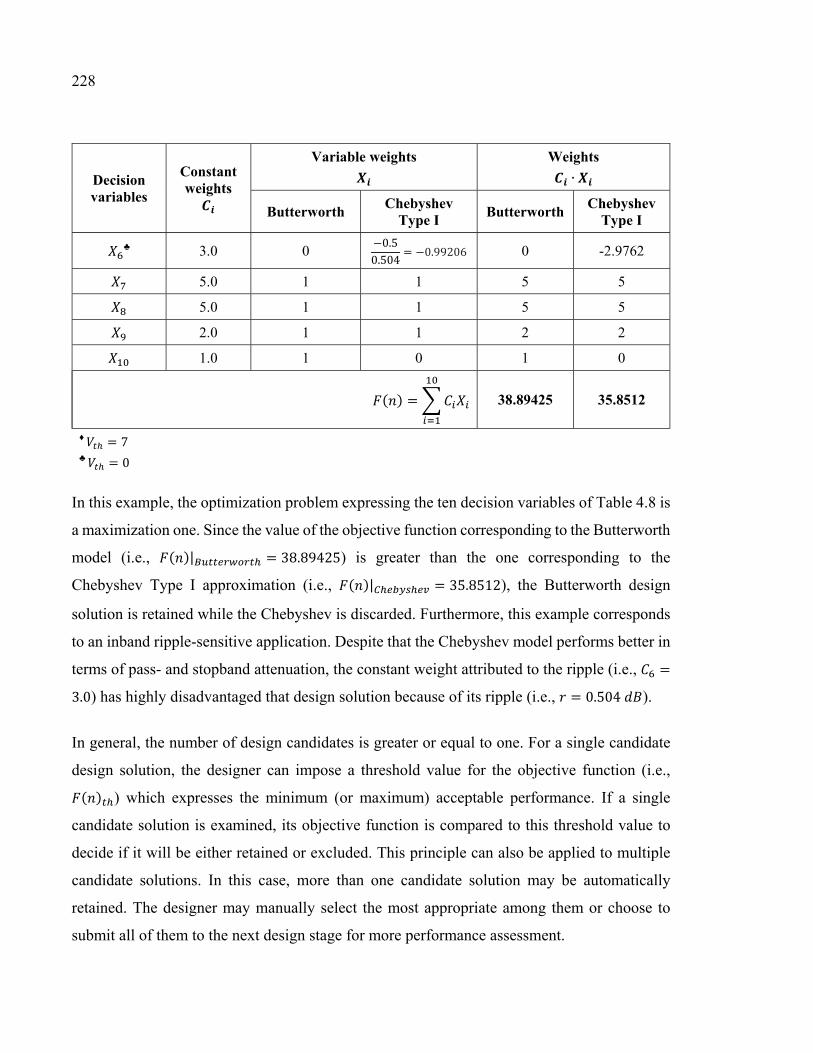
228
Decision variables
Constant weights
Variable weights
Weights ∙
Butterworth Chebyshev
Type I Butterworth
Chebyshev Type I
♣ 3.0 0 −0.50.504 = −0.99206 0 -2.9762
5.0 1 1 5 5
5.0 1 1 5 5
2.0 1 1 2 2
1.0 1 0 1 0
( ) = 38.89425 35.8512
♦ = 7 ♣ = 0
In this example, the optimization problem expressing the ten decision variables of Table 4.8 is
a maximization one. Since the value of the objective function corresponding to the Butterworth
model (i.e., ( )| = 38.89425) is greater than the one corresponding to the
Chebyshev Type I approximation (i.e., ( )| = 35.8512), the Butterworth design
solution is retained while the Chebyshev is discarded. Furthermore, this example corresponds
to an inband ripple-sensitive application. Despite that the Chebyshev model performs better in
terms of pass- and stopband attenuation, the constant weight attributed to the ripple (i.e., =3.0) has highly disadvantaged that design solution because of its ripple (i.e., = 0.504 ).
In general, the number of design candidates is greater or equal to one. For a single candidate
design solution, the designer can impose a threshold value for the objective function (i.e., ( ) ) which expresses the minimum (or maximum) acceptable performance. If a single
candidate solution is examined, its objective function is compared to this threshold value to
decide if it will be either retained or excluded. This principle can also be applied to multiple
candidate solutions. In this case, more than one candidate solution may be automatically
retained. The designer may manually select the most appropriate among them or choose to
submit all of them to the next design stage for more performance assessment.
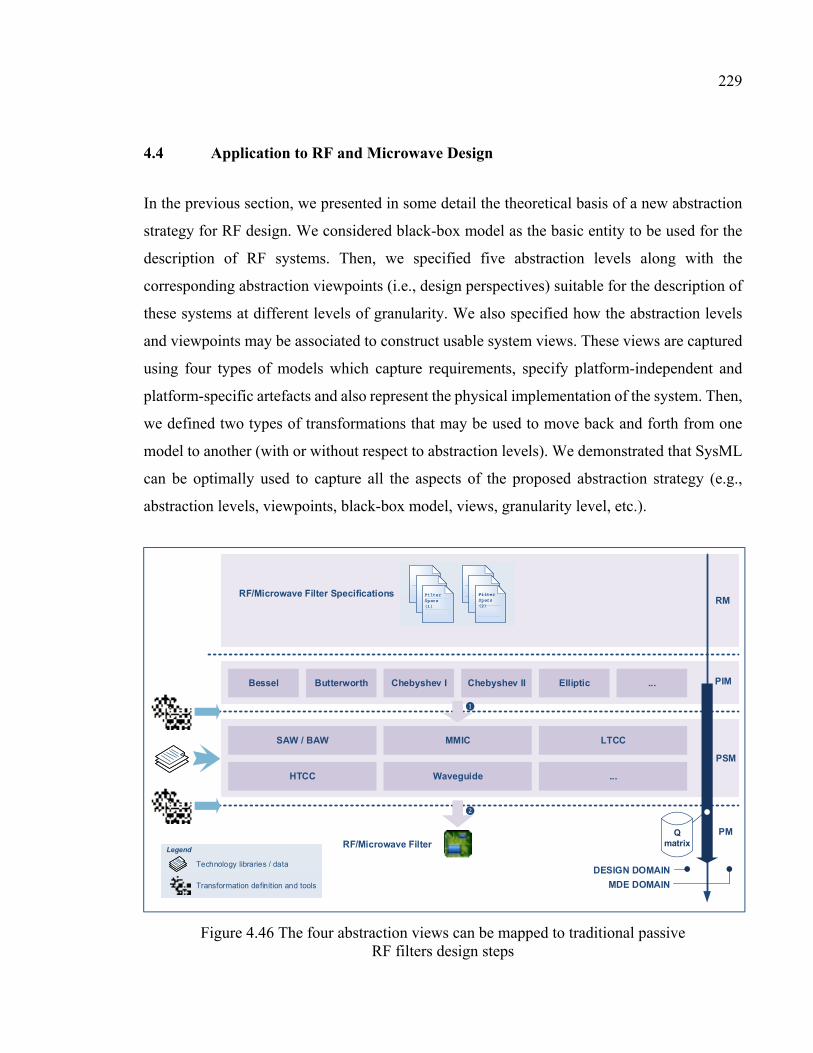
229
4.4 Application to RF and Microwave Design
In the previous section, we presented in some detail the theoretical basis of a new abstraction
strategy for RF design. We considered black-box model as the basic entity to be used for the
description of RF systems. Then, we specified five abstraction levels along with the
corresponding abstraction viewpoints (i.e., design perspectives) suitable for the description of
these systems at different levels of granularity. We also specified how the abstraction levels
and viewpoints may be associated to construct usable system views. These views are captured
using four types of models which capture requirements, specify platform-independent and
platform-specific artefacts and also represent the physical implementation of the system. Then,
we defined two types of transformations that may be used to move back and forth from one
model to another (with or without respect to abstraction levels). We demonstrated that SysML
can be optimally used to capture all the aspects of the proposed abstraction strategy (e.g.,
abstraction levels, viewpoints, black-box model, views, granularity level, etc.).
Chebyshev I
MDE DOMAIN
RF/Microwave Filter Specifications
ButterworthBessel Elliptic ...
LTCCMMICSAW / BAW
HTCC Waveguide ...
Chebyshev II
RF/Microwave FilterQ
matrix
PIM
PSM
PM
DESIGN DOMAIN
Transformation definition and tools
Legend
Technology libraries / data
Filter Specs (2)
FilterSpecs (1)
RM
❶
❷
Figure 4.46 The four abstraction views can be mapped to traditional passive RF filters design steps
230
In this section, we briefly investigate how the key concepts of the proposed abstraction strategy
may be applied to real RF systems. Two examples will be examined: passive filters and
operational amplifiers. It is worth noting that detailed case studies will be presented in chapter
5 for the purpose of validating the proposed approach.
a) RF passive filters
The traditional design approach for RF passive filters starts with specifications. Several models
of filters (e.g., Chebyshev, maximally flat, elliptic and Bessel) are thoroughly detailed in
literature. In general, these models are endorsed by appropriate mathematical formalisms that
allow the design of ideal filter prototypes which meet the initial specifications. Then, the ideal
filter elements are converted into real implementations in different technologies (i.e.,
waveguides, lumped components, LTCC, distributed lines, etc.).
As shown in Figure 4.46, the filter specifications may be captured using requirements models
(RMs). Since the ideal filter prototypes are equation-based and deliver ideal LC networks, they
can be considered as platform-independent models. If the specifications cannot be met by the
traditional filter models, a custom filter network (even approximate) may be constructed and
considered as a PIM. Given technology information, the resulting platform-independent model
may be converted into a platform-specific model using an appropriate transformation. Ideal
LC elements are replaced by real lumped-component electrical models or derived into
equivalent distributed lines. Finally, the final filter implementation (e.g., layout) is derived
from the PSM using a relevant tool or transformation. This results in a platform model that can
be manufactured and tested. Figure 4.46 maps the traditional design scheme with the different
abstraction views. It depicts also the regions where transformation rules and tools are required
as well as the technology input.
b) Operational Amplifiers
If we consider the design of a typical CMOS device such as an operational amplifier (OpAmp),
the main models to be developed using the proposed abstraction strategy are as follows:
− OpAmp Requirement and Platform-independent models: expressed in SysML, The
resulting models capture not only the functional parameters of an OpAmp but also can
231
include its specific requirements, constraints, behavior and internal structure. The top part
of Figure 4.47 shows various SysML diagrams describing the OpAmp specifications. For
example, the top diagram is the block definition diagram (bdd) and captures some key
parameters of the OpAmp such as the open loop gain and slew rate;
− OpAmp Platform-specific model: as mentioned above, the OpAmp PSM includes
technology considerations. For this case study, we chose CMOS as a reference technology.
This PSM, represented by a circuit schematic in which transistors are MOS devices
generated using the proper transformation from the OpAmp PIM is a proper technology-
dependent model (see middle part of Figure 4.47). One of the advantages of this
representation is the immediate use of available CAD tools, e.g., Cadence with a proper
technology file, to simulate and validate the PSM’s performance;
− OpAmp Implementation (i.e., platform model): an implementation of the OpAmp is a
ready-to-manufacture design. It is generally captured using a conventional layout that
captures all the relevant information needed for the fabrication of the OpAmp (see bottom
part of Figure 4.47). It can be subject of various performance assessments and
optimizations before it is submitted to fabrication process for final device manufacturing.
As shown in Figure 4.47, two transformations may be defined to move from PIM to PSM
and PSM to implementation respectively:
− PIM to PSM Transformation: as previously discussed, a transformation may be a set of
design rules, an algorithm or a tool that is able to interpret the PIM and then generate a
PSM that relates to a given fabrication technology. One of the reasons to choose the
OpAmp as an application example in this section is the abundance of OpAmp design
tutorials and procedures in the literature. For example, an OpAmp can be designed on the
basis of a differential folded cascode structure (Bako, Butkovic et Baric, 2010). A custom
CMOS OpAmp design methodology is presented in (Khare, Khare et Sethiya, 2008).
Detailed step-by step design tutorials of CMOS OpAmps are also thoroughly presented in
(Comer, 1985; Kao, Wei et Kuo, 2001). Accordingly, such a transformation can be
developed based on the existing body of literature and the OpAmp’s PIM description;
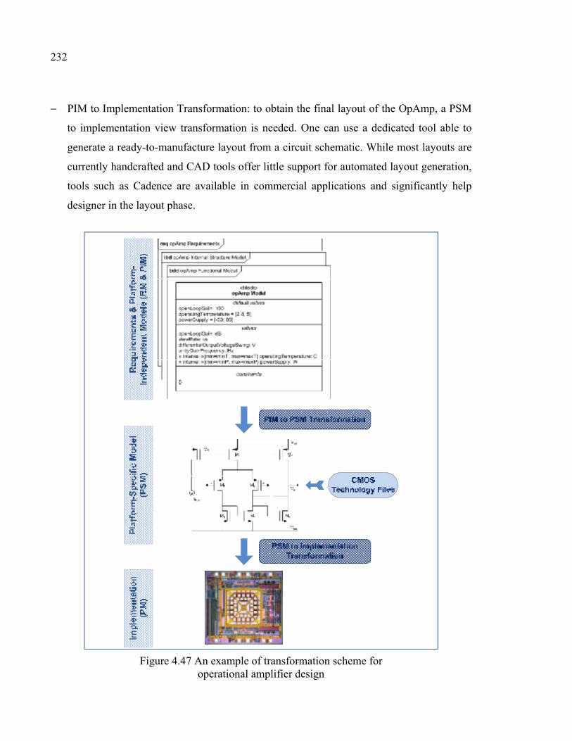
232
− PIM to Implementation Transformation: to obtain the final layout of the OpAmp, a PSM
to implementation view transformation is needed. One can use a dedicated tool able to
generate a ready-to-manufacture layout from a circuit schematic. While most layouts are
currently handcrafted and CAD tools offer little support for automated layout generation,
tools such as Cadence are available in commercial applications and significantly help
designer in the layout phase.
Figure 4.47 An example of transformation scheme for operational amplifier design
233
The examples of passive filters and operational amplifiers presented in this section show that
the main aspects of the proposed abstraction strategy are applicable to RF design. However,
we still need to streamline the developed abstraction concepts with the design scheme already
discussed in chapter 3. The ultimate goal is obtaining a relatively complete design framework
to endorse modern design practice of RF systems.
4.5 SysML Profile for RF Devices
In the previous sections (e.g., 4.3.3) we illustrated how SysML could be used for the modeling
of RF devices and the elaboration of high-level functional description. In this section, we
develop comprehensive constructs to facilitate such tasks. As shown in Figure 4.48, we use the
mechanism of profiling87 to extend the SysML standard with constructs adapted for the RF
domain. The elaboration of a “SysML Profile for RF Devices” aims at providing a basic
modeling infrastructure that can serve as a generic template for the development of SysML
models for RF devices and systems.
The proposed SysML profile uses the constructs (e.g., blocks, parts and relationships),
notations, semantics and diagrams in order to define a new meta-model which allows to model
the various aspects of RF devices and systems. As shown in the package diagram of Figure
4.49, the proposed SysML profile consists of four main meta-models:
− RF stereotypes: in modeling languages, a stereotype is construct that allows extending the
languages vocabulary by adding new modeling elements derived from existing ones but
having their own properties, attributes and constraints. The package « RF stereotypes »
defines specific blocks capturing the properties, structure and particularities of RF devices;
− Requirements: the package « Requirements » uses SysML requirement diagram and
constructs in order to capture common RF requirements in a set of template models;
87 “Profile” is an extension mechanism used to extend a reference meta-model (such as a modeling language, e.g., UML) with custom constructs that are specific to a particular domain.
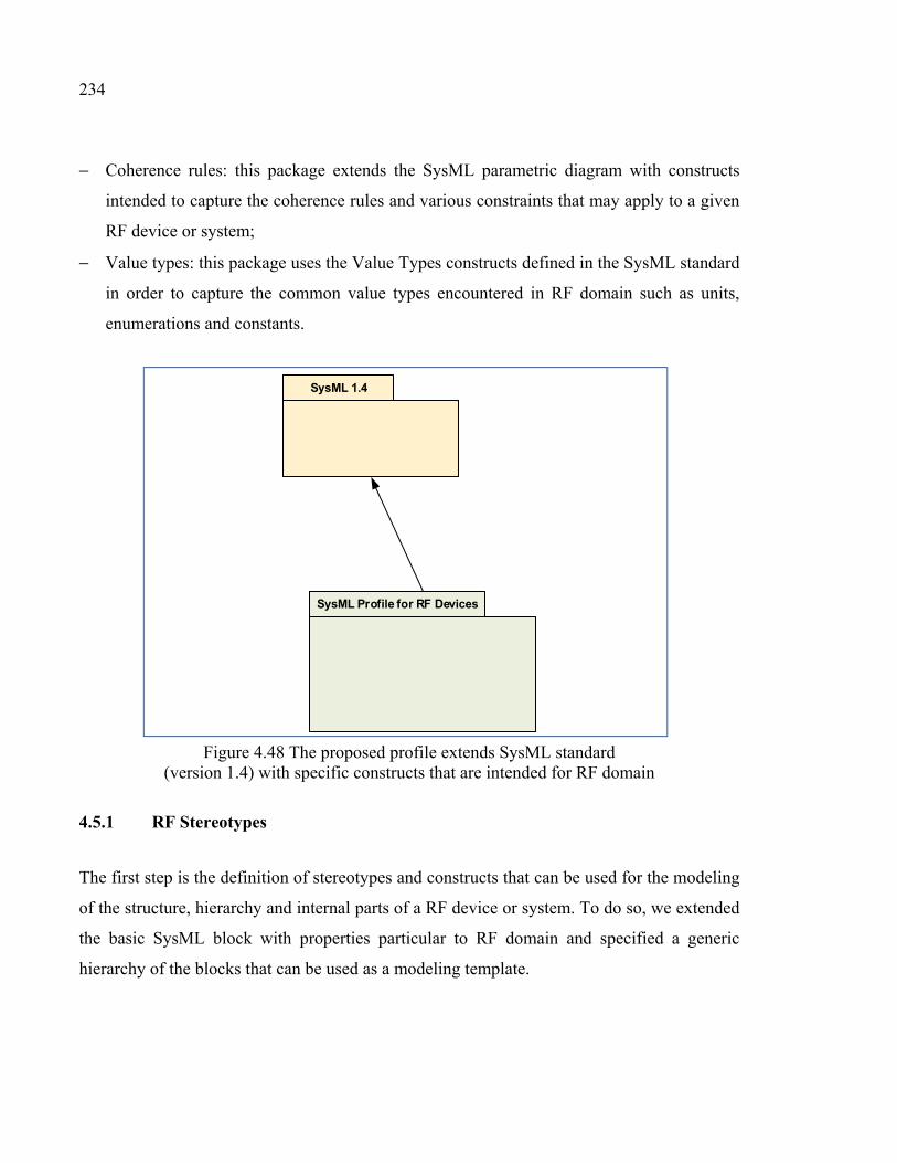
234
− Coherence rules: this package extends the SysML parametric diagram with constructs
intended to capture the coherence rules and various constraints that may apply to a given
RF device or system;
− Value types: this package uses the Value Types constructs defined in the SysML standard
in order to capture the common value types encountered in RF domain such as units,
enumerations and constants.
SysML 1.4
SysML Profile for RF Devices
Figure 4.48 The proposed profile extends SysML standard (version 1.4) with specific constructs that are intended for RF domain
4.5.1 RF Stereotypes
The first step is the definition of stereotypes and constructs that can be used for the modeling
of the structure, hierarchy and internal parts of a RF device or system. To do so, we extended
the basic SysML block with properties particular to RF domain and specified a generic
hierarchy of the blocks that can be used as a modeling template.
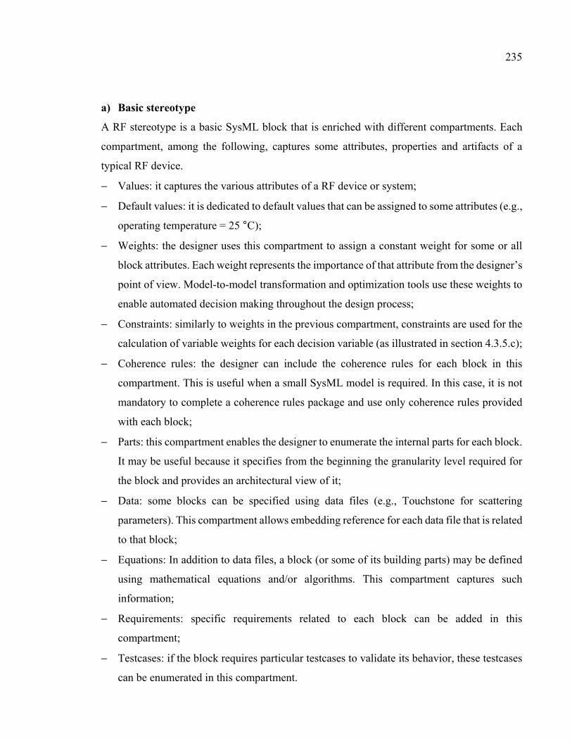
235
a) Basic stereotype
A RF stereotype is a basic SysML block that is enriched with different compartments. Each
compartment, among the following, captures some attributes, properties and artifacts of a
typical RF device.
− Values: it captures the various attributes of a RF device or system;
− Default values: it is dedicated to default values that can be assigned to some attributes (e.g.,
operating temperature = 25 °C);
− Weights: the designer uses this compartment to assign a constant weight for some or all
block attributes. Each weight represents the importance of that attribute from the designer’s
point of view. Model-to-model transformation and optimization tools use these weights to
enable automated decision making throughout the design process;
− Constraints: similarly to weights in the previous compartment, constraints are used for the
calculation of variable weights for each decision variable (as illustrated in section 4.3.5.c);
− Coherence rules: the designer can include the coherence rules for each block in this
compartment. This is useful when a small SysML model is required. In this case, it is not
mandatory to complete a coherence rules package and use only coherence rules provided
with each block;
− Parts: this compartment enables the designer to enumerate the internal parts for each block.
It may be useful because it specifies from the beginning the granularity level required for
the block and provides an architectural view of it;
− Data: some blocks can be specified using data files (e.g., Touchstone for scattering
parameters). This compartment allows embedding reference for each data file that is related
to that block;
− Equations: In addition to data files, a block (or some of its building parts) may be defined
using mathematical equations and/or algorithms. This compartment captures such
information;
− Requirements: specific requirements related to each block can be added in this
compartment;
− Testcases: if the block requires particular testcases to validate its behavior, these testcases
can be enumerated in this compartment.
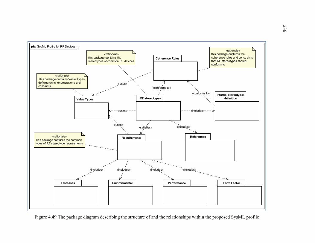
Value Types
pkg SysML Profile for RF Devices
«rationale»this package contains the stereotypes of common RF devices
RF stereotypes
«uses»
«rationale»This package contains Value Types defining units, enumerations and constants
References
«includes»
Coherence Rules
Requirements
Environmental Performance Form Factor
«includes»«includes»«includes»
«uses»
«uses»
Testcases
«includes»
Internal stereotypes definition
«includes»
«satisfies»
«conforms to»
«conforms to»
«rationale»This package captures the common types of RF stereotype requirements
«rationale»this package captures the coherence rules and constraints that RF stereotypes should conform to
Figure 4.49 The package diagram describing the structure of and the relationships within the proposed SysML profile
236
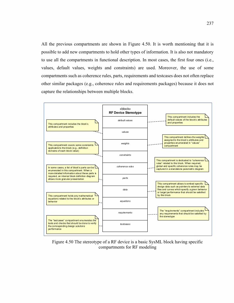
237
All the previous compartments are shown in Figure 4.50. It is worth mentioning that it is
possible to add new compartments to hold other types of information. It is also not mandatory
to use all the compartments in functional description. In most cases, the first four ones (i.e.,
values, default values, weights and constraints) are used. Moreover, the use of some
compartments such as coherence rules, parts, requirements and testcases does not often replace
other similar packages (e.g., coherence rules and requirements packages) because it does not
capture the relationships between multiple blocks.
«block»RF Device Stereotype
default values
values
weights
constraints
coherence rules
data
equations
requirements
This compartment includes the default values of the block’s attributes and properties
parts
This compartment defines the weights assigned to the block’s attributes and properties enumerated in “values” compartment
This compartment includes the block’s at tributes and properties
This compartment covers some constraints applicable to the block (e.g., definition domains of each block value)
This compartment is dedicated to “coherence rules” related to this block. When required, global and specific coherence rules may be captured in a standalone parametric diagram
In some cases, a list of block’s parts can be enumerated in this compartment. When a more detailed informat ion about these parts is required, an internal block def inition diagram allows more granular presentation
This compartment allows to embed specific design data such as pointers to external data files and curves which specify a given behavior or target performance that should be satisfied by this blockThis compartment holds any mathematical
equations related to the block’s attributes or behavior
The “requirements” compartment includes any requirements that should be satisfied by the stereotype
testcases
The “testcases” compartment enumerates the tests and checks that should be done to verify the corresponding design solutions performance
Figure 4.50 The stereotype of a RF device is a basic SysML block having specific compartments for RF modeling
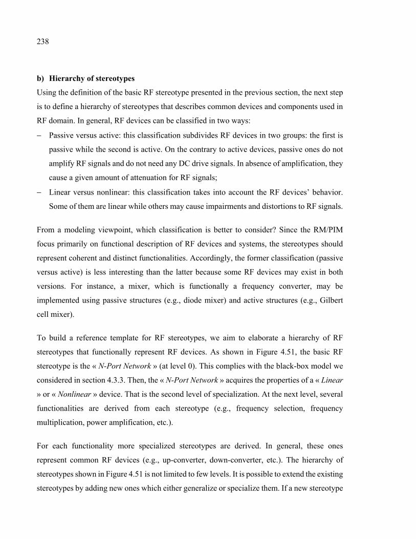
238
b) Hierarchy of stereotypes
Using the definition of the basic RF stereotype presented in the previous section, the next step
is to define a hierarchy of stereotypes that describes common devices and components used in
RF domain. In general, RF devices can be classified in two ways:
− Passive versus active: this classification subdivides RF devices in two groups: the first is
passive while the second is active. On the contrary to active devices, passive ones do not
amplify RF signals and do not need any DC drive signals. In absence of amplification, they
cause a given amount of attenuation for RF signals;
− Linear versus nonlinear: this classification takes into account the RF devices’ behavior.
Some of them are linear while others may cause impairments and distortions to RF signals.
From a modeling viewpoint, which classification is better to consider? Since the RM/PIM
focus primarily on functional description of RF devices and systems, the stereotypes should
represent coherent and distinct functionalities. Accordingly, the former classification (passive
versus active) is less interesting than the latter because some RF devices may exist in both
versions. For instance, a mixer, which is functionally a frequency converter, may be
implemented using passive structures (e.g., diode mixer) and active structures (e.g., Gilbert
cell mixer).
To build a reference template for RF stereotypes, we aim to elaborate a hierarchy of RF
stereotypes that functionally represent RF devices. As shown in Figure 4.51, the basic RF
stereotype is the « N-Port Network » (at level 0). This complies with the black-box model we
considered in section 4.3.3. Then, the « N-Port Network » acquires the properties of a « Linear
» or « Nonlinear » device. That is the second level of specialization. At the next level, several
functionalities are derived from each stereotype (e.g., frequency selection, frequency
multiplication, power amplification, etc.).
For each functionality more specialized stereotypes are derived. In general, these ones
represent common RF devices (e.g., up-converter, down-converter, etc.). The hierarchy of
stereotypes shown in Figure 4.51 is not limited to few levels. It is possible to extend the existing
stereotypes by adding new ones which either generalize or specialize them. If a new stereotype
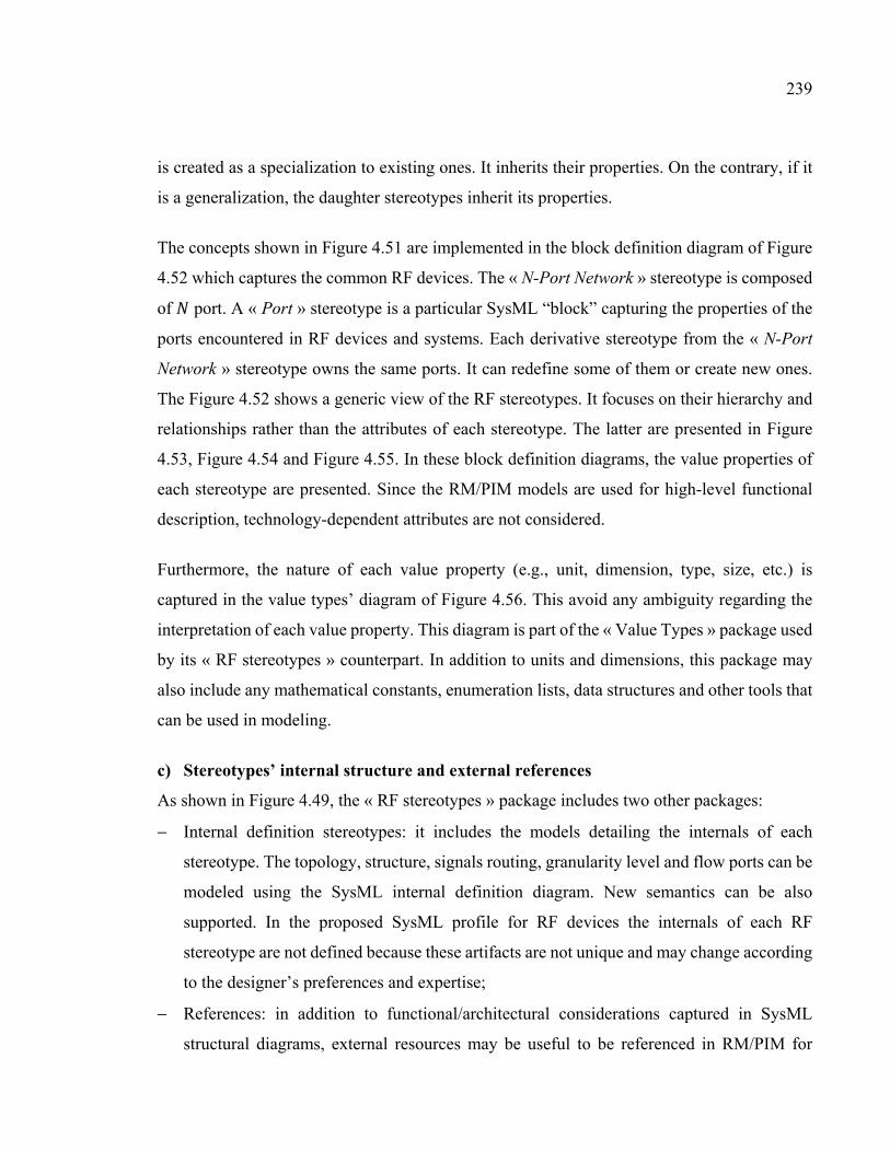
239
is created as a specialization to existing ones. It inherits their properties. On the contrary, if it
is a generalization, the daughter stereotypes inherit its properties.
The concepts shown in Figure 4.51 are implemented in the block definition diagram of Figure
4.52 which captures the common RF devices. The « N-Port Network » stereotype is composed
of port. A « Port » stereotype is a particular SysML “block” capturing the properties of the
ports encountered in RF devices and systems. Each derivative stereotype from the « N-Port
Network » stereotype owns the same ports. It can redefine some of them or create new ones.
The Figure 4.52 shows a generic view of the RF stereotypes. It focuses on their hierarchy and
relationships rather than the attributes of each stereotype. The latter are presented in Figure
4.53, Figure 4.54 and Figure 4.55. In these block definition diagrams, the value properties of
each stereotype are presented. Since the RM/PIM models are used for high-level functional
description, technology-dependent attributes are not considered.
Furthermore, the nature of each value property (e.g., unit, dimension, type, size, etc.) is
captured in the value types’ diagram of Figure 4.56. This avoid any ambiguity regarding the
interpretation of each value property. This diagram is part of the « Value Types » package used
by its « RF stereotypes » counterpart. In addition to units and dimensions, this package may
also include any mathematical constants, enumeration lists, data structures and other tools that
can be used in modeling.
c) Stereotypes’ internal structure and external references
As shown in Figure 4.49, the « RF stereotypes » package includes two other packages:
− Internal definition stereotypes: it includes the models detailing the internals of each
stereotype. The topology, structure, signals routing, granularity level and flow ports can be
modeled using the SysML internal definition diagram. New semantics can be also
supported. In the proposed SysML profile for RF devices the internals of each RF
stereotype are not defined because these artifacts are not unique and may change according
to the designer’s preferences and expertise;
− References: in addition to functional/architectural considerations captured in SysML
structural diagrams, external resources may be useful to be referenced in RM/PIM for
240
better traceability. These external resources include but not limited to design data, tools
and specific files (e.g., schematics, workspaces, etc.). The « References » package does not
compromise the highest level of abstraction required for a RM/PIM. It links this abstract
functional description to resources that are useful for throughout the design cycle.
4.5.2 Coherence Rules and Requirements
To capture the text requirements, the structural packages (i.e., the « RF stereotypes » and its
included packages) are accompanied with the « Requirements » package. If these packages
should satisfy certain preset rules, the « Coherence rules » package provides constructs to
capture them. Both packages are depicted in Figure 4.49.
a) Coherence rules
The « Coherence rules » package reuses the SysML parametric diagram to capture the
coherence rules used in the validation process of the functional description (including
structural diagrams and requirements). These rules (commonly mathematical) are not only
limited to RF stereotypes but can also be extended to their relationships and their internal parts.
In addition, this package includes any design constraints expressed in the specifications.
b) Requirements
The « Requirement » package is intended to provide an infrastructure that allows capturing the
common requirements related to RF design. This package makes use of the various SysML
requirements constructs (e.g., the requirement diagram) in order to meet this goal. In the
proposed SysML profile, we suggest an infrastructure composed of three main composite
requirement constructs:
− Performance: this construct holds the requirements related to RF device’s performance. At
this regard, we consider requirements in terms of linear, nonlinear and noise performance.
For each category, we also consider appropriate testcases;
− Form factor: this construct captures the requirements related to the device’s physical and
mechanical aspects and appearance (e.g., size, weight, shape, etc.).
N-Port Network
Non-Linear Device Linear Device New N-Port Network Device
Detection DevicePower Amplifier
Device
Frequency Multiplication Device
New Non-Linear Device…
…
Power Isolation and Circulation Device
Port Transformation Device
Generic Two-Port Device
New Linear Device…
…Power Attenuation
Device
Frequency Selection Device
New Generic Two-Port Device…
Phase Shifting Device
Lowpass-HighpassFilter Device
Bandpass-BandstopFilter Device
New Frequency Selection Device
……
Up-Conversion DeviceDown-Conversion
Device
New Frequency Multiplication Device
…
New Device
Level 0
Level 1
Level 2
Level 3
Level 4
Level N
• Level 0: the highest abstraction level• The level i is a specialization of the level i-1• New Device stereotype allows the extension of
the model by the creation of new devices models• Level N: there is no practical limit to extensions
Figure 4.51 At the functional level, RF stereotypes are hierarchically structured 241
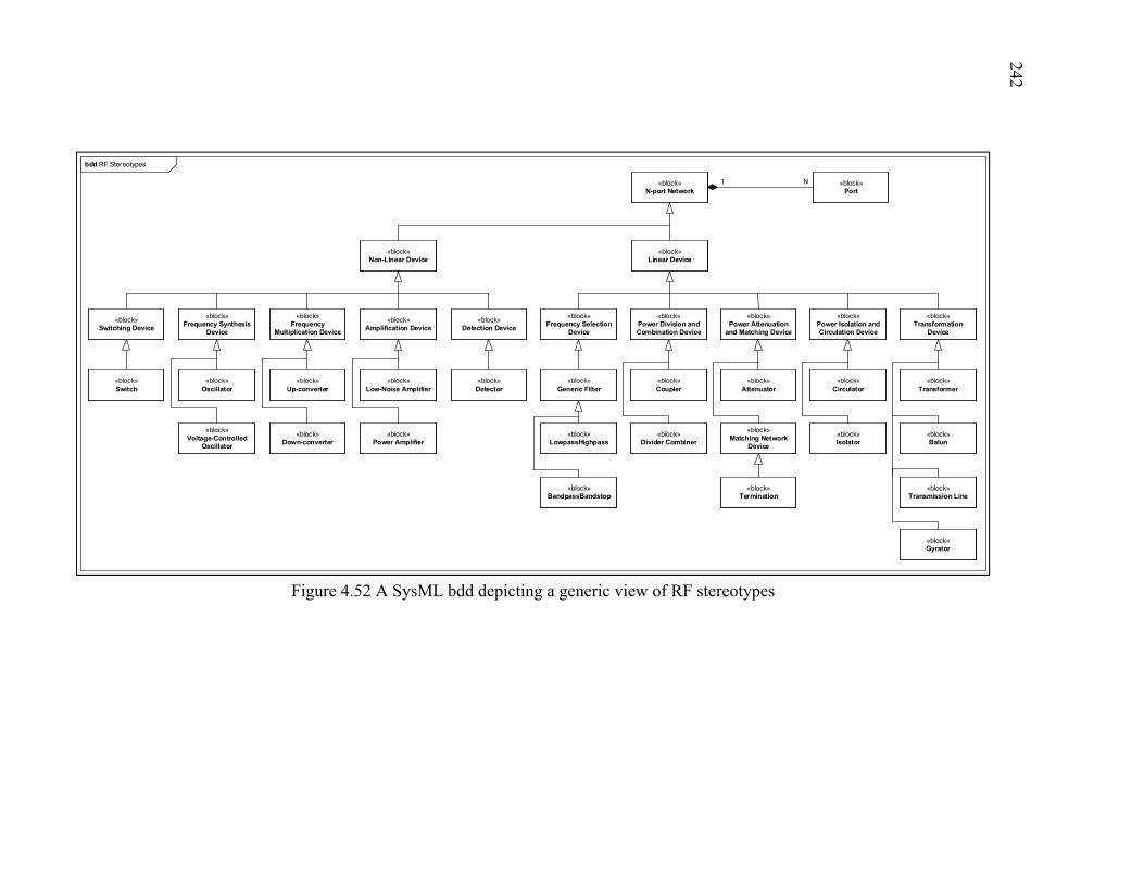
242
bdd RF Stereotypes
«block»N-port Network
«block»Non-Linear Device
«block»Linear Device
«block»Port
1 N
«block»Amplification Device
«block»Detection Device
«block»Frequency
Multiplication Device
«block»Frequency Synthesis
Device
«block»Switching Device
«block»Power Amplifier
«block»Voltage-Controlled
Oscillator
«block»Down-converter
«block»Frequency Selection
Device
«block»Power Attenuation
and Matching Device
«block»Power Isolation and Circulation Device
«block»Transformation
Device
«block»BandpassBandstop
«block»Divider Combiner
«block»Termination
«block»Isolator
«block»Balun
«block»Transmission Line
«block»Gyrator
«block»Matching Network
Device
«block»LowpassHighpass
«block»Switch
«block»Low-Noise Amplifier
«block»Detector
«block»Oscillator
«block»Up-converter
«block»Generic Filter
«block»Coupler
«block»Attenuator
«block»Circulator
«block»Transformer
«block»Power Division and Combination Device
Figure 4.52 A SysML bdd depicting a generic view of RF stereotypes
242
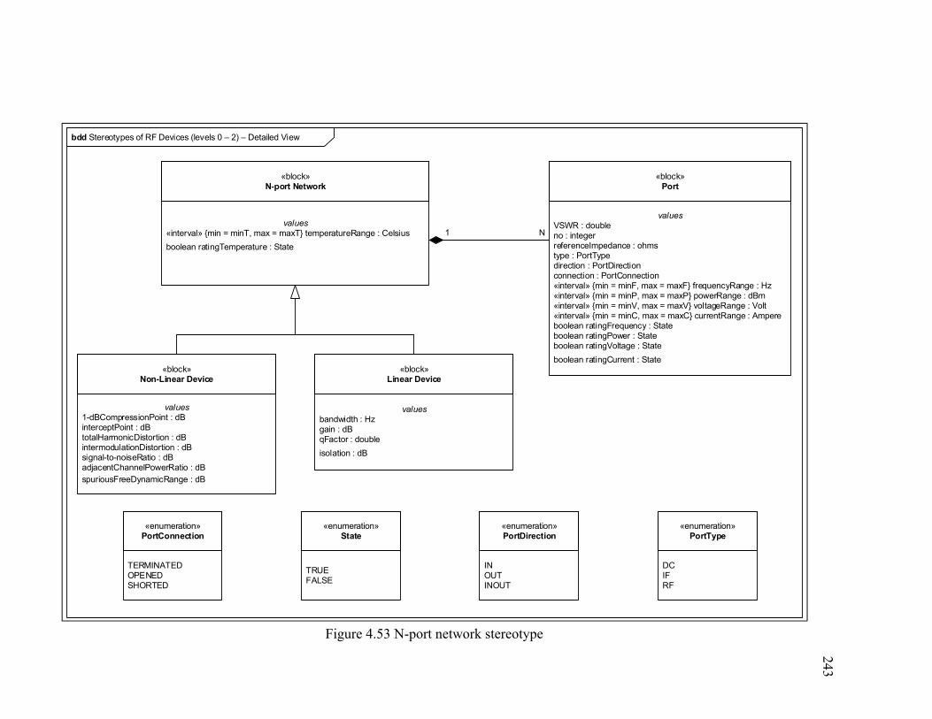
243
bdd Stereotypes of RF Devices (levels 0 – 2) – Detailed View
«block»N-port Network
«block»Non-Linear Device
«block»Linear Device
«block»Port
1 Nvalues
«interval» min = minT, max = maxT temperatureRange : Celsius
boolean ratingTemperature : State
valuesVSWR : doubleno : integerreferenceImpedance : ohmstype : PortTypedirection : PortDirectionconnection : PortConnection«interval» min = minF, max = maxF frequencyRange : Hz«interval» min = minP, max = maxP powerRange : dBm«interval» min = minV, max = maxV voltageRange : Volt«interval» min = minC, max = maxC currentRange : Ampereboolean ratingFrequency : Stateboolean ratingPower : Stateboolean ratingVoltage : State
boolean ratingCurrent : State
valuesbandwidth : Hzgain : dBqFactor : double
isolation : dB
values1-dBCompressionPoint : dBinterceptPoint : dBtotalHarmonicDistortion : dBintermodulationDistortion : dBsignal-to-noiseRatio : dBadjacentChannelPowerRatio : dBspuriousFreeDynamicRange : dB
«enumeration»PortConnection
TERMINATEDOPENEDSHORTED
«enumeration»State
TRUEFALSE
«enumeration»PortDirection
INOUTINOUT
«enumeration»PortType
DCIFRF
Figure 4.53 N-port network stereotype
243
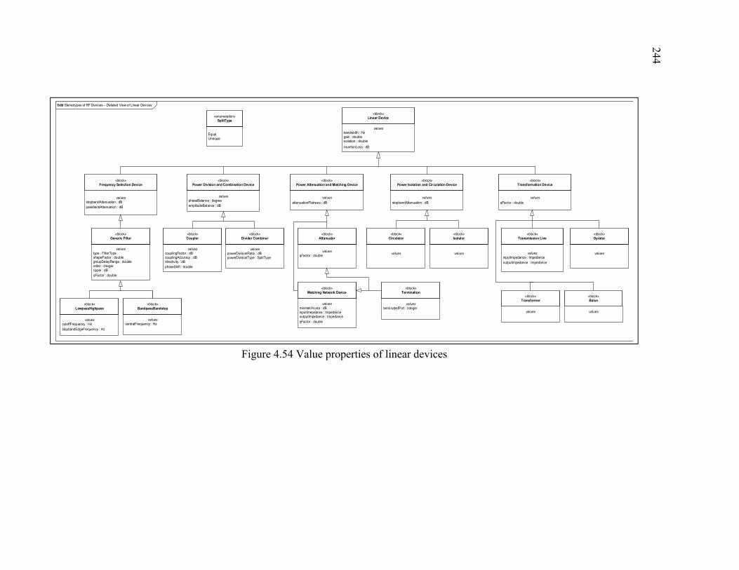
244
bdd Stereotypes of RF Devices – Detailed View of Linear Devices
valuesstopbandAttenuation : dBpassbandAttenuation : dB
«block»Frequency Selection Device
«block»Power Division and Combination Device
valuesphaseBalance : degreeamplitudeBalance : dB
«block»Power Attenuation and Matching Device
valuesattenuationFlatness : dB
«block»Transformation Device
valuesqFactor : double
valuestype : FilterTypeshapeFactor : doublegroupDelayRange : doubleorder : integerripple : dBqFactor : double
«block»Generic Filter
valuescouplingFactor : dBcouplingAccuracy : dBdirectivity : dBphaseShift : double
«block»Coupler
valuespowerDivisionRatio : dBpowerDivisionType : SplitType
«block»Divider Combiner
valuesqFactor : double
«block»Attenuator
values
«block»Circulator
values
«block»Isolator
«block»Power Isolation and Circulation Device
valuesstopbandAttenuation : dB
valuesinputImpedance : ImpedanceoutputImpedance : Impedance
«block»Transmission Line
values
«block»Gyrator
values
«block»Transformer
values
«block»Balun
valuesmismatchLoss : dBinputImepdance : ImpedanceoutputImpedance : ImpedanceqFactor : double
«block»Matching Network Device
valuescutoffFrequency : HzstopbandEdgeFrequency : Hz
valuescentralFrequency : Hz
«block»LowpassHighpass
«block»BandpassBandstop
«enumeration»SplitType
EqualUnequal
valuesbandwidth : Hzgain : doubleisolation : double
insertionLoss : dB
«block»Linear Device
valuesterminatedPort : integer
«block»Termination
Figure 4.54 Value properties of linear devices
244
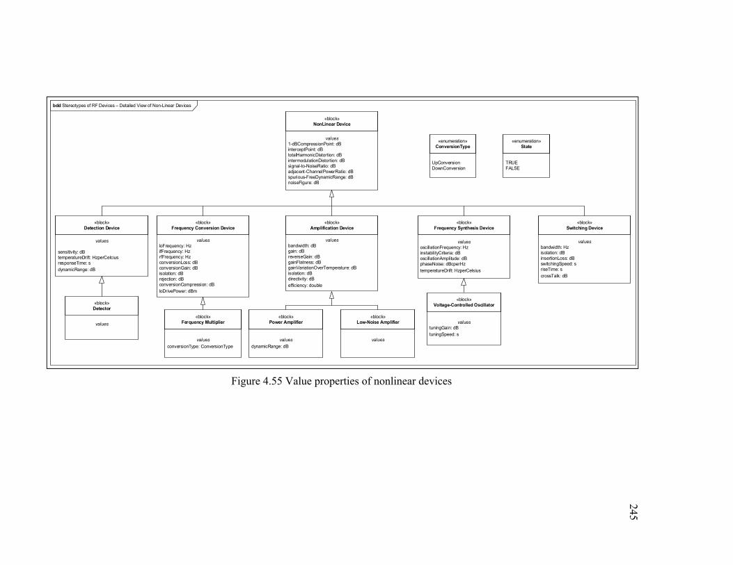
245
bdd Stereotypes of RF Devices – Detailed View of Non-Linear Devices
«block»Detection Device
«block»NonLinear Device
values1-dBCompressionPoint: dBinterceptPoint: dBtotalHarmonicDistortion: dBintermodulationDistortion: dBsignal-to-NoiseRatio: dBadjacent-ChannelPowerRatio: dBspurious-FreeDynamicRange: dBnoiseFigure: dB
values
sensitivity: dBtemperatureDrift: HzperCelciusresponseTime: sdynamicRange: dB
«block»Frequency Conversion Device
valuesloFrequency: HzifFrequency: HzrfFrequency: HzconversionLoss: dBconversionGain: dBisolation: dBrejection: dBconversionCompression: dBloDrivePower: dBm
«block»Amplification Device
valuesbandwidth: dBgain: dBreverseGain: dBgainFlatness: dBgainVariationOverTemperature: dBisolation: dBdirectivity: dBefficiency: double
«block»Switching Device
valuesbandwidth: Hzisolation: dBinsertionLoss: dBswitchingSpeed: sriseTime: scrossTalk: dB
values
«block»Detector
valuestuningGain: dBtuningSpeed: s
«enumeration»ConversionType
UpConversionDownConversion
«enumeration»State
TRUEFALSE
«block»Frequency Synthesis Device
valuesoscillationFrequency: HzinstabilityCriteria: dBoscillationAmplitude: dBphaseNoise: dBcperHztemperatureDrift: HzperCelsius
valuesdynamicRange: dB
«block»Power Amplifier
values
«block»Low-Noise Amplifier
valuesconversionType: ConversionType
«block»Ferquency Multiplier
«block»Voltage-Controlled Oscillator
Figure 4.55 Value properties of nonlinear devices
245
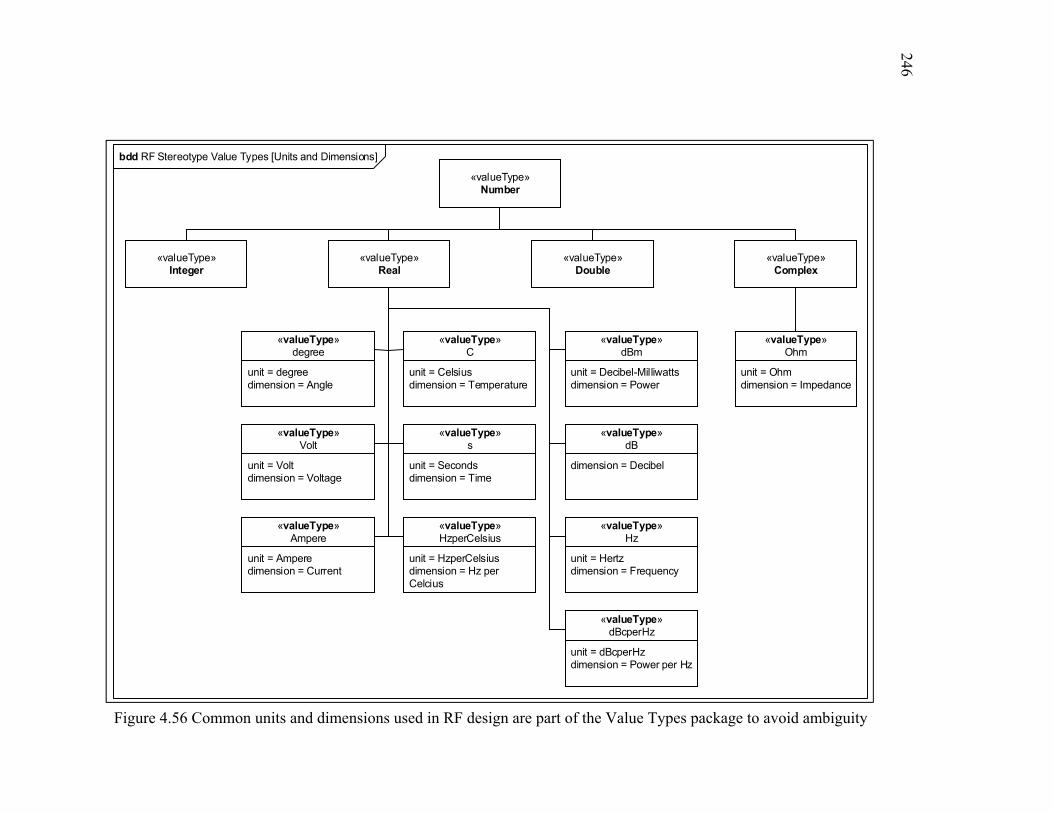
246
bdd RF Stereotype Value Types [Units and Dimensions]
«valueType»Complex
unit = Ohmdimension = Impedance
«valueType»Ohm
«valueType»Integer
«valueType»Double
«valueType»Number
«valueType»Real
unit = Celsiusdimension = Temperature
«valueType»C
unit = Secondsdimension = Time
«valueType»s
unit = HzperCelsiusdimension = Hz per Celcius
«valueType»HzperCelsius
unit = Voltdimension = Voltage
«valueType»Volt
unit = degreedimension = Angle
«valueType»degree
unit = Amperedimension = Current
«valueType»Ampere
unit = Decibel-Milliwattsdimension = Power
«valueType»dBm
dimension = Decibel
«valueType»dB
unit = Hertzdimension = Frequency
«valueType»Hz
unit = dBcperHzdimension = Power per Hz
«valueType»dBcperHz
Figure 4.56 Common units and dimensions used in RF design are part of the Value Types package to avoid ambiguity
246
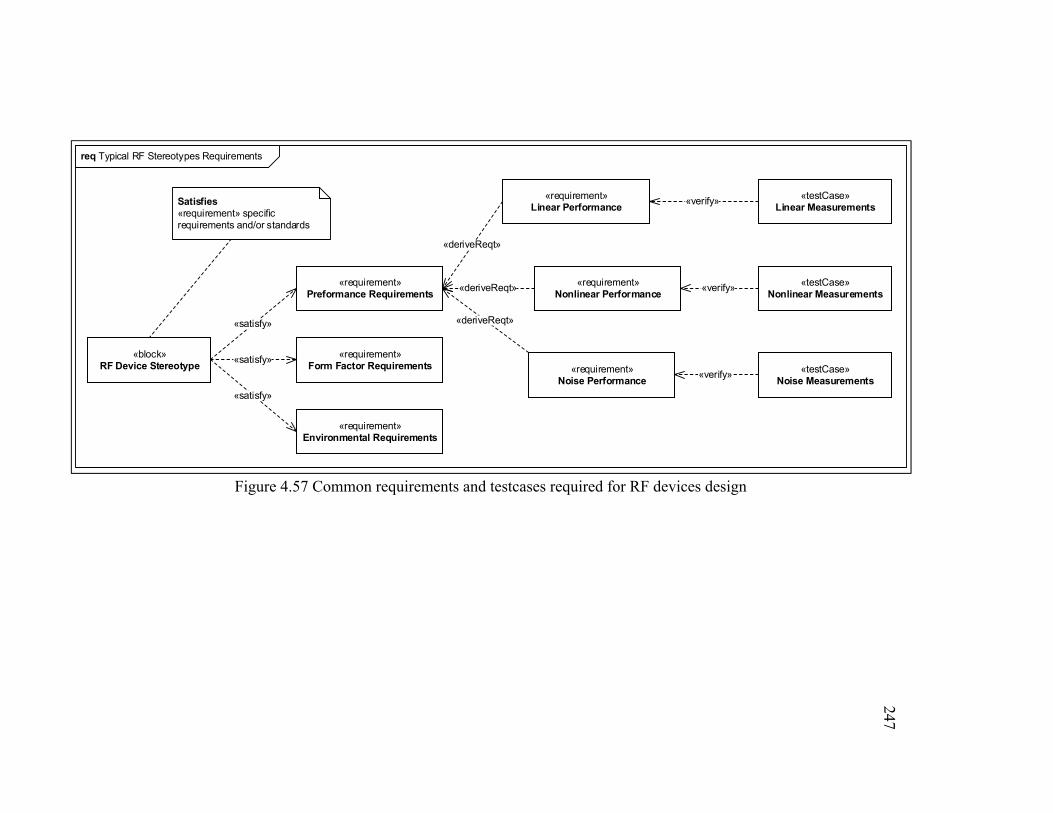
247
req Typical RF Stereotypes Requirements
«satisfy»
«block»RF Device Stereotype
«requirement»Preformance Requirements
«requirement»Form Factor Requirements
«satisfy»
«requirement»Environmental Requirements
«satisfy»
«testCase»Linear Measurements
«verify»Satisfies«requirement» specific requirements and/or standards
«requirement»Noise Performance
«deriveReqt»
«requirement»Linear Performance
«deriveReqt»
«requirement»Nonlinear Performance
«deriveReqt» «testCase»Nonlinear Measurements
«testCase»Noise Measurements
«verify»
«verify»
Figure 4.57 Common requirements and testcases required for RF devices design
247
248
− Environmental: the environmental requirements include radiation, shielding and other
metrics measuring the device’s effect on its environment. This type of requirements is
captured using the environmental requirement construct.
The Figure 4.57 depicts the previous requirement constructs and their related testcases.
4.5.3 Profile Extension and Usage
The proposed SysML profile aims at enabling a design template to help beginners coping with
functional description of RF devices and systems using the Systems Modeling Language. For
this reason, it intentionally provides simple constructs and reuses the same semantics of
SysML. That is why it does not cover necessarily all the existing RF devices. The proposed
packages (including stereotypes attributes and relationships) are not exhaustive. Nevertheless,
it is always possible to enrich this profile with new design constructs to model more
complicated RF devices and systems.
a) Altering the proposed constructs
Using SysML constructs (such as blocks, parts and diagrams), it is always possible to modify
the proposed profile. These modifications include the alteration of the attributes, relationships
and semantics related to each construct (e.g., adding or removing attributes form an existing
RF stereotype). It also includes the redefinition, deletion or replacement of existing ones (e.g.,
adding or removing stereotypes or packages). Existing constructs can also be rearranged.
To illustrate these principles, we altered the RF stereotypes of Figure 4.52 as depicted in Figure
4.58 in order to model linear two-port devices. For this purpose, we first created a new
stereotype named « Generic Two-Port Device » (red-colored in Figure 4.58). The new
stereotype is a generalization of existing ones (i.e., « Transformation Device », « Power
Attenuation and Matching Device » and « Frequency Selection Device »). Since all the
daughter stereotypes of the « Transformation Device » one (e.g., transformers and baluns) are
not two-port devices, we rearranged the remaining stereotypes in a new hierarchy (as depicted
in the green rectangle of Figure 4.58). The retained stereotypes (i.e., « Transmission Line »
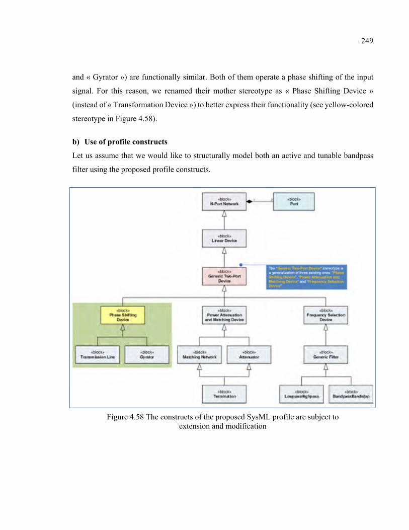
249
and « Gyrator ») are functionally similar. Both of them operate a phase shifting of the input
signal. For this reason, we renamed their mother stereotype as « Phase Shifting Device »
(instead of « Transformation Device ») to better express their functionality (see yellow-colored
stereotype in Figure 4.58).
b) Use of profile constructs
Let us assume that we would like to structurally model both an active and tunable bandpass
filter using the proposed profile constructs.
Figure 4.58 The constructs of the proposed SysML profile are subject to extension and modification
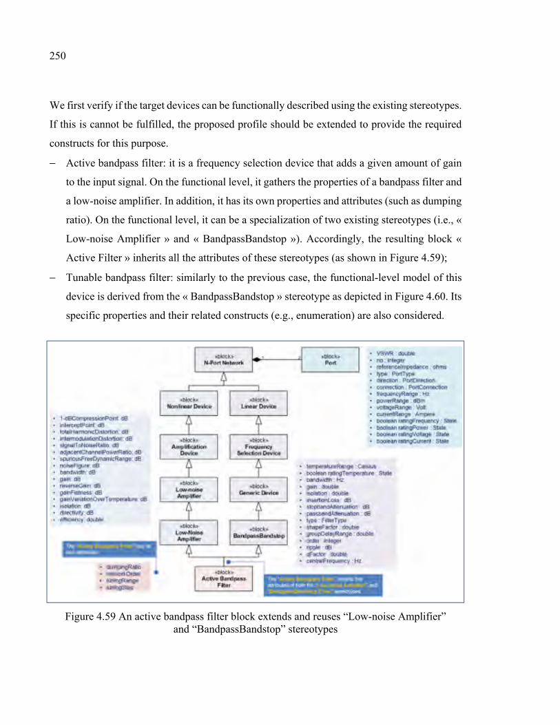
250
We first verify if the target devices can be functionally described using the existing stereotypes.
If this is cannot be fulfilled, the proposed profile should be extended to provide the required
constructs for this purpose.
− Active bandpass filter: it is a frequency selection device that adds a given amount of gain
to the input signal. On the functional level, it gathers the properties of a bandpass filter and
a low-noise amplifier. In addition, it has its own properties and attributes (such as dumping
ratio). On the functional level, it can be a specialization of two existing stereotypes (i.e., «
Low-noise Amplifier » and « BandpassBandstop »). Accordingly, the resulting block «
Active Filter » inherits all the attributes of these stereotypes (as shown in Figure 4.59);
− Tunable bandpass filter: similarly to the previous case, the functional-level model of this
device is derived from the « BandpassBandstop » stereotype as depicted in Figure 4.60. Its
specific properties and their related constructs (e.g., enumeration) are also considered.
Figure 4.59 An active bandpass filter block extends and reuses “Low-noise Amplifier” and “BandpassBandstop” stereotypes
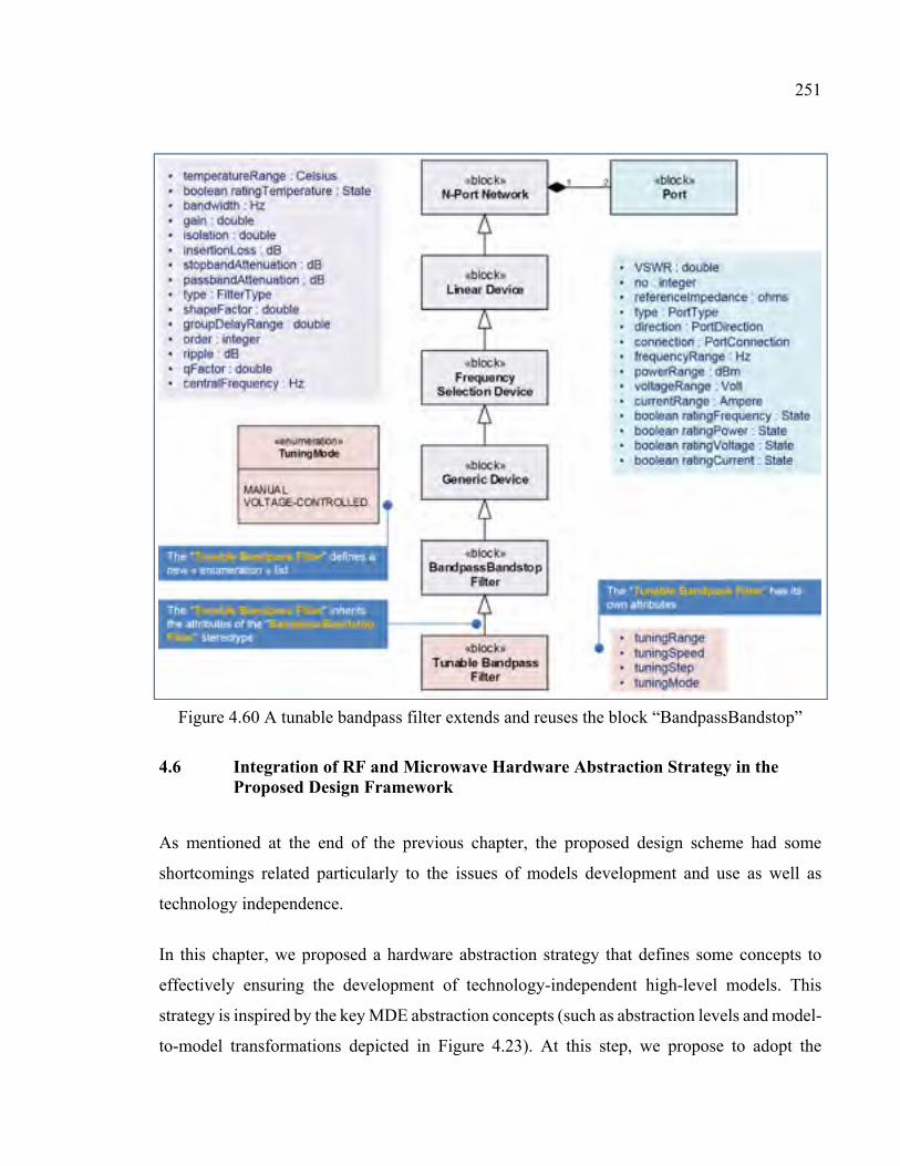
251
Figure 4.60 A tunable bandpass filter extends and reuses the block “BandpassBandstop”
4.6 Integration of RF and Microwave Hardware Abstraction Strategy in the
Proposed Design Framework
As mentioned at the end of the previous chapter, the proposed design scheme had some
shortcomings related particularly to the issues of models development and use as well as
technology independence.
In this chapter, we proposed a hardware abstraction strategy that defines some concepts to
effectively ensuring the development of technology-independent high-level models. This
strategy is inspired by the key MDE abstraction concepts (such as abstraction levels and model-
to-model transformations depicted in Figure 4.23). At this step, we propose to adopt the
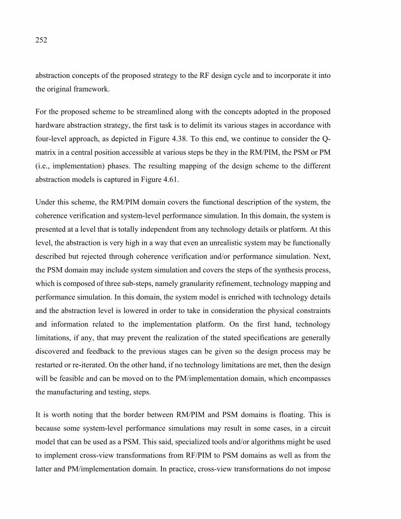
252
abstraction concepts of the proposed strategy to the RF design cycle and to incorporate it into
the original framework.
For the proposed scheme to be streamlined along with the concepts adopted in the proposed
hardware abstraction strategy, the first task is to delimit its various stages in accordance with
four-level approach, as depicted in Figure 4.38. To this end, we continue to consider the Q-
matrix in a central position accessible at various steps be they in the RM/PIM, the PSM or PM
(i.e., implementation) phases. The resulting mapping of the design scheme to the different
abstraction models is captured in Figure 4.61.
Under this scheme, the RM/PIM domain covers the functional description of the system, the
coherence verification and system-level performance simulation. In this domain, the system is
presented at a level that is totally independent from any technology details or platform. At this
level, the abstraction is very high in a way that even an unrealistic system may be functionally
described but rejected through coherence verification and/or performance simulation. Next,
the PSM domain may include system simulation and covers the steps of the synthesis process,
which is composed of three sub-steps, namely granularity refinement, technology mapping and
performance simulation. In this domain, the system model is enriched with technology details
and the abstraction level is lowered in order to take in consideration the physical constraints
and information related to the implementation platform. On the first hand, technology
limitations, if any, that may prevent the realization of the stated specifications are generally
discovered and feedback to the previous stages can be given so the design process may be
restarted or re-iterated. On the other hand, if no technology limitations are met, then the design
will be feasible and can be moved on to the PM/implementation domain, which encompasses
the manufacturing and testing, steps.
It is worth noting that the border between RM/PIM and PSM domains is floating. This is
because some system-level performance simulations may result in some cases, in a circuit
model that can be used as a PSM. This said, specialized tools and/or algorithms might be used
to implement cross-view transformations from RF/PIM to PSM domains as well as from the
latter and PM/implementation domain. In practice, cross-view transformations do not impose
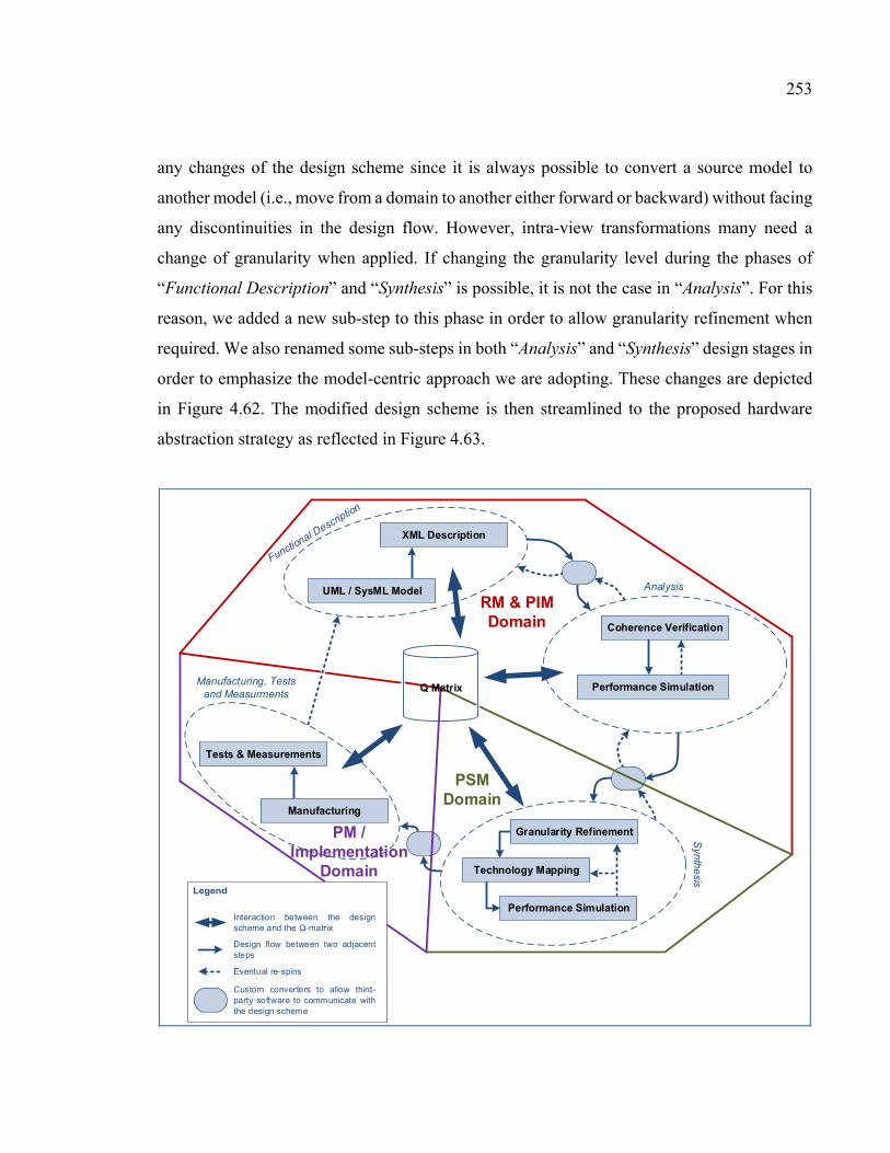
253
any changes of the design scheme since it is always possible to convert a source model to
another model (i.e., move from a domain to another either forward or backward) without facing
any discontinuities in the design flow. However, intra-view transformations many need a
change of granularity when applied. If changing the granularity level during the phases of
“Functional Description” and “Synthesis” is possible, it is not the case in “Analysis”. For this
reason, we added a new sub-step to this phase in order to allow granularity refinement when
required. We also renamed some sub-steps in both “Analysis” and “Synthesis” design stages in
order to emphasize the model-centric approach we are adopting. These changes are depicted
in Figure 4.62. The modified design scheme is then streamlined to the proposed hardware
abstraction strategy as reflected in Figure 4.63.
XML Description
Manufacturing
Tests & Measurements
UML / SysML Model Analysis
Syn
the
sis
Manufacturing, Tests and Measurments
Interaction between the design scheme and the Q-matrix
Design flow between two adjacent steps
Custom converters to allow third-party software to communicate with the design scheme
Technology Mapping
Granularity Refinement
Performance Simulation
Performance Simulation
Coherence Verification
Eventual re-spins
RM & PIM Domain
PM / Implementation
Domain
PSM Domain
Q Matrix
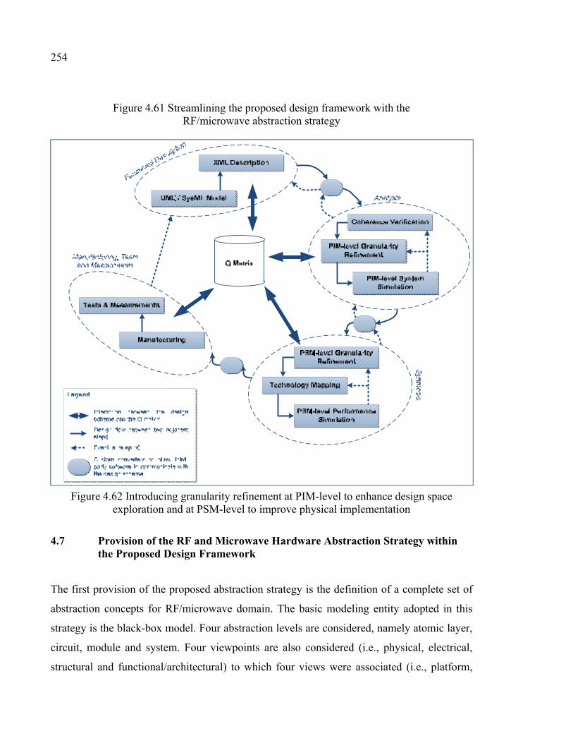
254
Figure 4.61 Streamlining the proposed design framework with the RF/microwave abstraction strategy
Figure 4.62 Introducing granularity refinement at PIM-level to enhance design space exploration and at PSM-level to improve physical implementation
4.7 Provision of the RF and Microwave Hardware Abstraction Strategy within
the Proposed Design Framework
The first provision of the proposed abstraction strategy is the definition of a complete set of
abstraction concepts for RF/microwave domain. The basic modeling entity adopted in this
strategy is the black-box model. Four abstraction levels are considered, namely atomic layer,
circuit, module and system. Four viewpoints are also considered (i.e., physical, electrical,
structural and functional/architectural) to which four views were associated (i.e., platform,
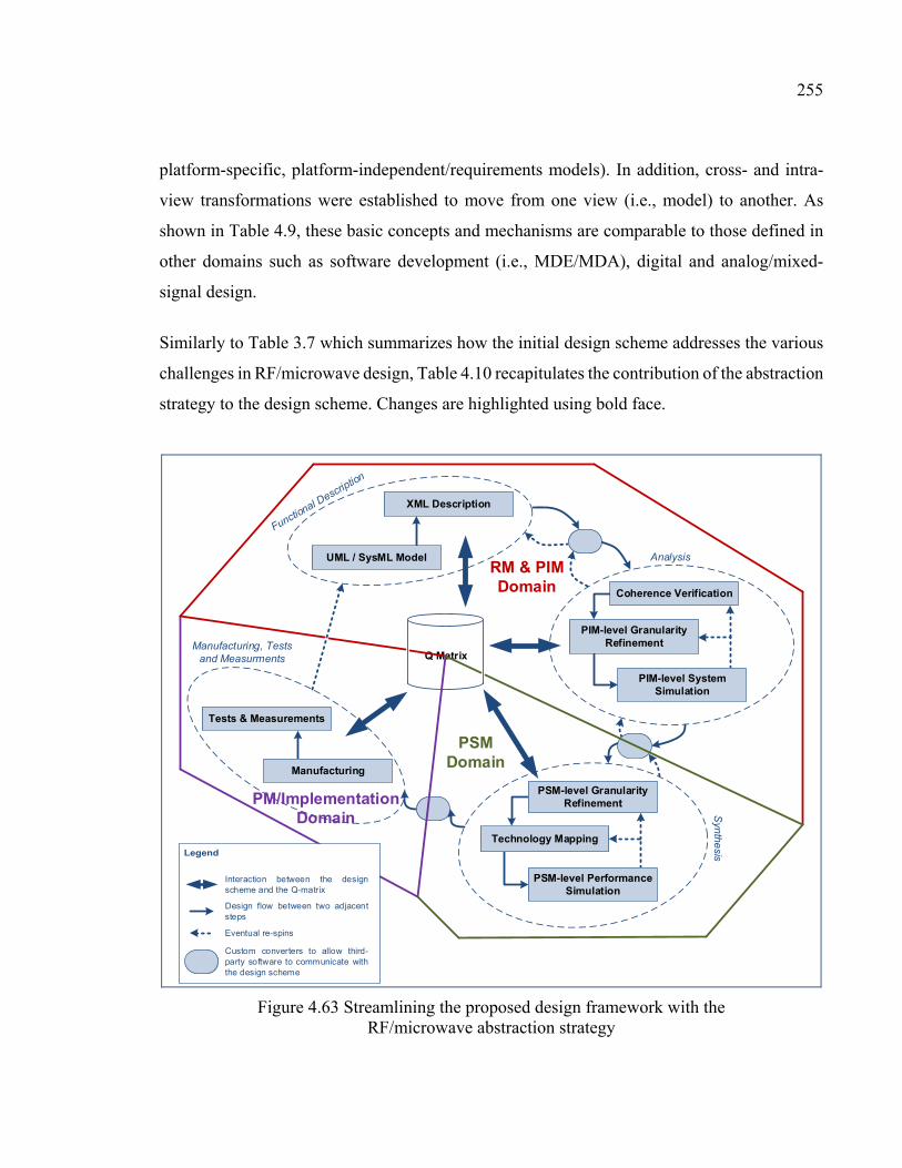
255
platform-specific, platform-independent/requirements models). In addition, cross- and intra-
view transformations were established to move from one view (i.e., model) to another. As
shown in Table 4.9, these basic concepts and mechanisms are comparable to those defined in
other domains such as software development (i.e., MDE/MDA), digital and analog/mixed-
signal design.
Similarly to Table 3.7 which summarizes how the initial design scheme addresses the various
challenges in RF/microwave design, Table 4.10 recapitulates the contribution of the abstraction
strategy to the design scheme. Changes are highlighted using bold face.
XML Description
PIM-level Granularity Refinement
Coherence Verification
Q Matrix
Manufacturing
Technology Mapping
PSM-level Granularity Refinement
Tests & Measurements
UML / SysML Model Analysis
Syn
thesis
Manufacturing, Tests and Measurments
PSM-level Performance Simulation
PIM-level System Simulation
RM & PIM Domain
PSM Domain
PM/Implementation Domain
Interaction between the design scheme and the Q-matrix
Design flow between two adjacent steps
Custom converters to allow third-party software to communicate with the design scheme
Eventual re-spins
Figure 4.63 Streamlining the proposed design framework with the RF/microwave abstraction strategy
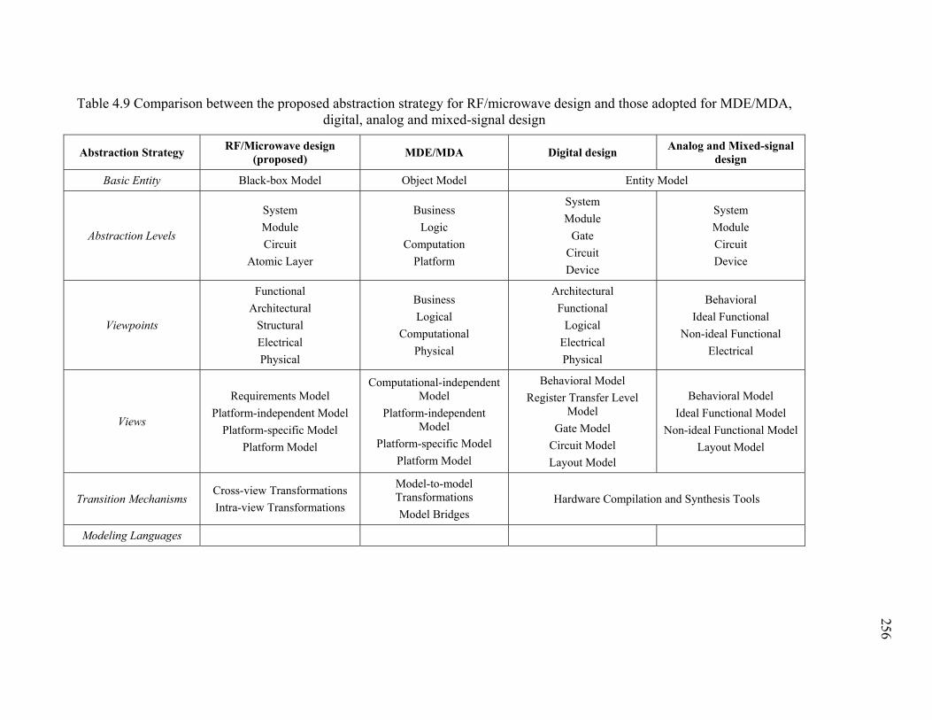
Table 4.9 Comparison between the proposed abstraction strategy for RF/microwave design and those adopted for MDE/MDA, digital, analog and mixed-signal design
Abstraction Strategy RF/Microwave design
(proposed) MDE/MDA Digital design
Analog and Mixed-signal design
Basic Entity Black-box Model Object Model Entity Model
Abstraction Levels
System
Module
Circuit
Atomic Layer
Business
Logic
Computation
Platform
System
Module
Gate
Circuit
Device
System
Module
Circuit
Device
Viewpoints
Functional
Architectural
Structural
Electrical
Physical
Business
Logical
Computational
Physical
Architectural
Functional
Logical
Electrical
Physical
Behavioral
Ideal Functional
Non-ideal Functional
Electrical
Views
Requirements Model
Platform-independent Model
Platform-specific Model
Platform Model
Computational-independent Model
Platform-independent Model
Platform-specific Model
Platform Model
Behavioral Model
Register Transfer Level Model
Gate Model
Circuit Model
Layout Model
Behavioral Model
Ideal Functional Model
Non-ideal Functional Model
Layout Model
Transition Mechanisms Cross-view Transformations
Intra-view Transformations
Model-to-model Transformations
Model Bridges Hardware Compilation and Synthesis Tools
Modeling Languages
256
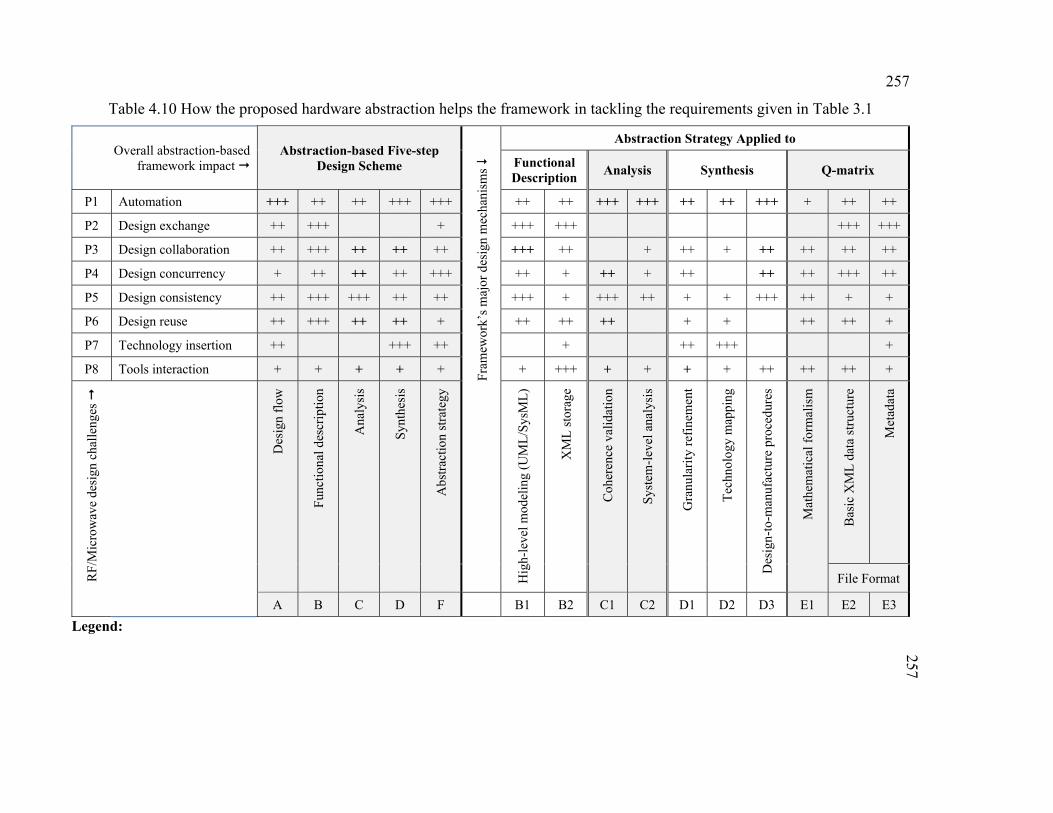
257
Table 4.10 How the proposed hardware abstraction helps the framework in tackling the requirements given in Table 3.1
Overall abstraction-based framework impact
Abstraction-based Five-step Design Scheme
Abstraction Strategy Applied to
Fra
mew
ork’
s m
ajor
des
ign
mec
hani
sms Functional
Description Analysis Synthesis Q-matrix
P1 Automation +++ ++ ++ +++ +++ ++ ++ +++ +++ ++ ++ +++ + ++ ++
P2 Design exchange ++ +++ + +++ +++ +++ +++
P3 Design collaboration ++ +++ ++ ++ ++ +++ ++ + ++ + ++ ++ ++ ++
P4 Design concurrency + ++ ++ ++ +++ ++ + ++ + ++ ++ ++ +++ ++
P5 Design consistency ++ +++ +++ ++ ++ +++ + +++ ++ + + +++ ++ + +
P6 Design reuse ++ +++ ++ ++ + ++ ++ ++ + + ++ ++ +
P7 Technology insertion ++ +++ ++ + ++ +++ +
P8 Tools interaction + + + + + + +++ + + + + ++ ++ ++ +
RF
/Mic
row
ave
desi
gn c
halle
nges
Des
ign
flow
Fun
ctio
nal d
escr
iptio
n
Ana
lysi
s
Syn
thes
is
Abs
trac
tion
str
ateg
y
Hig
h-le
vel m
odel
ing
(UM
L/S
ysM
L)
XM
L s
tora
ge
Coh
eren
ce v
alid
atio
n
Sys
tem
-lev
el a
naly
sis
Gra
nula
rity
ref
inem
ent
Tec
hnol
ogy
map
ping
Des
ign-
to-m
anuf
actu
re p
roce
dure
s
Mat
hem
atic
al f
orm
alis
m
Bas
ic X
ML
dat
a st
ruct
ure
Met
adat
a
File Format
A B C D F B1 B2 C1 C2 D1 D2 D3 E1 E2 E3
Legend:
257
258
The model-to-model transformations concept adopted in the proposed hardware abstraction
strategy paves the way for increasing automation. Given the appropriate tools and/or
algorithms, the conversion of models becomes highly automated (or at least semi-automated,
especially if the designer wants to have more control of the design process). Better automation
comes also with better design concurrency because models can always be used in various
contexts (e.g., co-design, distributed computation tools, etc.). Being model-centric, tools
interaction improves gradually as well. Tasks such as coherence verification, system-level
analysis and synthesis take part of growing automation which significantly enhances designer
productivity. In addition, the control of abstraction levels associated to the Q-matrix
contributes to better productivity. This is because the design and simulation effort required at
high levels is smaller than at lower ones. Since the Q-matrix is always able to hold data design
related to different contexts, the designer can have access to data of different abstraction levels.
This gives the designer the ability of comparing the design performance at different levels of
complexity. This data may also serve for future designs as initial design solutions.
The definition of views and viewpoints allows for easier design collaboration since models
become more comprehensive and traceable. At this regard, design reuse is also enhanced
particularly at “Analysis” and “Synthesis” design stages.
4.8 Conclusion
The fourth chapter of this thesis begins with an overview of the strategies of hardware
abstraction in use in different engineering domains. We started with the abstraction concepts
applied in digital and analog/mixed-signal design. At this regard, we focused on abstraction
levels and concepts and how they fit within the design approaches in use in these domains.
Then, we broaden our survey of existing hardware abstraction strategies in other engineering
domains (e.g., software engineering). We learned from this survey which abstraction concepts
to elaborate for an effective abstraction strategy as well as how to implement and use models
at different abstraction levels and from various design standpoints. These observations helped
us in the elaboration of a hardware abstraction strategy for RF devices and systems.
259
The proposed abstraction strategy defines a set of abstraction mechanisms. First, it defines a
basic entity, namely black-box model, which serves as a generic model functionally
characterizing RF/microwave devices and circuits. Then, we define five abstraction levels,
viewpoints and views, which enable the designer to develop models from different design
perspectives and at various levels of abstraction. Next, we define the transition mechanisms
(i.e., intra- and cross-view transformations) that allow deriving a target model from another
one. These transformations are not only intended to provide practical ways to move from an
abstraction level to another (or changing the design viewpoint within the same abstraction
level) but also to automate that transition. We completed the proposed abstraction strategy with
a SysML profile for RF devices, a modeling infrastructure enabling designers to use SysML
for the functional description of RF devices and systems. This SysML extension adapting the
constructs of SysML to RF domain does not only support the key abstraction mechanisms (e.g.,
viewpoints, abstraction levels, granularity, etc.) but also provides visual diagrams for the
expression of design requirements and constraints. Finally, we streamlined the proposed
hardware abstraction strategy with the design cycle proposed in the previous chapter. The
combination of both resulted in a design framework that provides model-centric design stages
and a set of mechanisms to validate, optimize and automate the design solution search and
implementation.
This chapter concludes the second section of this thesis. The next chapter focuses on the
practical usage of the design framework. Through selected case studies, the various design
concepts and mechanisms are questioned in the purpose of validating the proposed design
framework.

CHAPTER 5
VALIDATION OF THE PROPOSED FRAMEWORK THROUGH SELECTED CASE STUDIES
5.1 Introduction
In the previous section, we proposed a new design framework for RF and microwave devices.
This framework consists of a five-step design cycle along with an adapted hardware abstraction
strategy. We introduced in this proposal diverse concepts to address the major challenges
(especially those related to productivity, collaboration and technology insertion) facing today’s
design practice. Since we have been so far limited to examples illustrating how the presented
mechanisms and concepts work, we aim in this chapter to validate the framework’s
applicability and coherence. Unfortunately, the formal validation of this framework falls
beyond the scope of this thesis for two main reasons. First, the originality of the framework
made it very difficult to develop appropriate tools for an end-to-end design process. That is
why we attempted to adapt some existing design packages and use them in our case studies.
Then, formal validation of the framework requires the elaboration of rigorous mathematical
models for each concept in order to validate the overall framework’s construction. This task
requires a huge effort and a focused expertise that is worth providing in future phases of the
framework development (e.g., eventual adoption in commercial applications).
The validation method we choose to adopt in this chapter is through selected design case
studies of both linear and nonlinear RF devices. We start with a reminder of the framework’s
design stages and concepts. Then, we present three design case studies. The first is a detailed
step-by-step design tutorial of RF bandpass filters using the proposed framework. The second
shows how to use multiple model-to-model transformations in PSM generation. The third
demonstrates concurrent design of attenuators. Additional but less detailed case studies of
nonlinear devices and system-level systems are presented at the end of the chapter. For each
case study, the role of the Q-matrix is underlined. Finally, we summarize the advances
provided by the framework in the light of the current design practice.
262
5.2 Practical Implementation of the Proposed Framework
As shown in Figure 4.59, the proposed framework consists of five-stage design scheme that is
built around the Q-matrix. This design scheme is streamlined with a hardware abstraction
strategy that defines three modeling views: Requirements and Platform-Independent Models,
Platform-Specific Models and Platform Models (see Figure 4.60). Each view expresses a given
design viewpoint that can be associated to a given abstraction level. These theoretical concepts
need to be implemented from a practical standpoint in a set of comprehensive steps where
inputs and outputs of each step are clear. Figure 5.1 depicts a flat representation of the design
framework from the designer’s perspective. The design process goes step-by-step through the
five-stage design cycle as illustrated in the flowchart of Figure 5.2:
a) UML/SysML Models
This step starts the design process. It requires a mandatory input, namely specifications. These
specifications may be in text format, spreadsheets, etc. The designer uses a model creation tool
to capture these specifications in SysML models (other standard modeling languages can also
be used). The models can be created from scratch or using existing modeling templates (e.g.,
modeling profiles). If the latter solution is adopted, the designer’s derives the required
functionality from the existing constructs (e.g., describing predefined functionalities).
Depending on that functionality, default parameters’ values are used to define the device’s
models. It is worth noting that both requirements and platform-independent models are
produced in this step. As SysML/UML standard languages are concerned, there is a number of
commercial software packages that can be used to capture specifications and produce visual
RM/PIM models. Most of these software tools are standalone packages that were mainly
optimized to be used in software engineering. Thus, they require some modifications to be used
in RF design. Ideally, any integrated design environment that is intended to make this
framework effective requires a dedicated software tool or plugin that is fully optimized for RF
modeling using standard modeling languages. At the end of UML/SysML modeling, the output
of this step is a set of files which holds the visual UML/SysML models representing the
device’s RM/PIM models.
263
b) XML Description
The RM/PIM models produced in the previous step are used at this level to generate
corresponding XML description. For this purpose, the designer uses a XML generation tool to
convert visual models into XML markup language files that can be automatically processed,
updated and exchanged between different tools, designers and design environments. Similarly
to modeling packages, there are currently existing tools mostly originating from software
engineering domain that fulfill this task. They can be adapted to RF design as well. The
generation of XML files is accompanied with the creation of the Q-matrix. At this level, it is
populated only with a subset of the data captured in RM/PIM models. Since these models are
not yet verified, they may contain errors and incoherencies and subsequently contaminate the
Q-matrix.
c) Coherence Verification
In this step, the RM/PIM models and XML files along with the associated Q-matrix are
validated to ensure the coherence of the models’ parameters and data. To this end, the designer
uses a model validation tool that checks the RM/PIM models based on a set of coherence
verification rules which are provided also as input. The tool produces a validation report where
any potential inconsistencies and validation errors are outlined. If errors reported, the designer
proceeds to the revision and correction of the RM/PIM models before it attempts to generate
again the corresponding XML description and Q-matrix and carry out another coherence
verification test. If all models and the related Q-matrix are proven to be coherent, the designer
can proceed to the next step where a design solution can be searched and optimized.
Unfortunately, there are no existing tools that can be used with no or at least minor
modifications to carry out the task of coherence verification. To overcome this weakness, we
used scripting languages to accomplish this process. Some specialized software libraries can
also be used for the same purpose (e.g., analog filter libraries).
d) PIM-level Granularity Refinement
Based on the RM/PIM models, the designer undertakes a space exploration process to look for
a solution that satisfies the initial requirements. If a promising design solution is found, this
step may be skipped. If no satisfactory solution is found, the designer proceeds to the
264
refinement of the PIM models in order to relax the design constraints. For example, if there are
any parameters that are overestimated, they might be given more reasonable values. If any key
design parameters were assigned to default values (particularly when design templates are
used), these defaults may be subject to review in order to make design solution search more
efficient. In all these cases, another coherence verification test is mandatory to keep the
RM/PIM models consistent and be sure that the new modifications did not compromise their
coherence. Having done this and no satisfactory design solution is found, the next action is
PIM-level granularity refinement that consists of changing the design view without changing
neither the abstraction level nor the design viewpoint. This is practically demonstrated by the
derivation of additional information within the models in the purpose of reducing the design
space search area. For every granularity refinement iteration, a new QBlock is added to the Q-
matrix to hold the data related to the RM/PIM models corresponding to that iteration. To
succeed the granularity refinement process, the designer uses jointly two main tools: a model
refiner and a model optimizer. Among the existing design tools, we noticed that scripting
languages may be used as refinement (and optimization) tools at a reasonable time and effort
cost. Some specialized commercial packages might also be used for the optimization of certain
models (often with significant overhead). In fact, an effort of manual models conversion should
be carried out in order to transform them into an acceptable input to these tools.
e) PIM-level Simulation
In this step, the designer carries out different simulations in order to ensure that the design
solution meets the requirements expressed by the RM/PIM models. Generally, it consists of
iterative performance evaluations (based on metrics mostly depending on the selected
functionality) and optimizations. Designers can use scripting and programming languages as
well as available APIs to carry out the required simulations for performance assessment. Most
system-level tools can be used but require an overhead due to manual adaptation of RM/PIM
models to the target design environment. During the PIM-level simulations, the Q-matrix is
regularly updated. At every iteration, one or many new QBlocks can also be added. Feeding
continuously the Q-matrix with data is useful for various purposes (e.g., conducting a
performance comparison between multiple candidate design solutions). Using a relevant
model-to-model transformation, one or many PSMs are synthesized from the best PIM-level
265
candidate design solution. Therefore, the output of this step is one or many platform-specific
design solutions (i.e., PSM). In addition, an up-to-date Q-matrix which holds the history of the
design process so far is also obtained. The original models (especially RMs often used for
validation and traceability) are frequently attached to the resulting PSMs for the next design
steps.
f) PSM-level Granularity Refinement
It is the first step in the synthesis design stage. The platform-specific design solution (i.e.,
PSM) already created using a PIM-to-PSM transformation is augmented with platform-specific
information only (e.g., target implementation technology such as distributed lines).
Nevertheless, it does not necessary encompass detailed platform information (e.g., substrate
data, technology constraints, etc.). That is why technology input is required to complete the
model information. Before technology mapping, the PSM is assessed against the requirements.
If the PSM does not satisfy the requirements, granularity refinement attempts to enhance the
quality of that design solution. For example, a new QBlock is added to the Q-matrix in order
to capture the corresponding design data.
g) Technology Mapping
At this step, the resulting PSM is augmented with detailed technology information. In practice,
this means that each PSM element is enriched with corresponding technology features and
items (e.g., substrate, physical characteristics and constraints, physical shapes and dimensions,
etc.). Technology information may be provided using component libraries, electrical models
or some existing tools (such as ADS LineCalc) that can be used to synthesize the physical
properties of each PSM element. Ideally, this process is fully automated which implies the use
of specialized tools that can automatically map each PSM component to the corresponding
technology details. For the following case studies, we used scripting and programming
languages for this purpose.
h) PSM-level Performance Simulation
Given a PSM with detailed technology information, the designer conducts at this level several
performance simulations in order to evaluate the PSM’s response against the requirements. At
266
this step, the performance assessment of the PSM is more accurate than its predecessor (i.e.,
PIM) due to the availability of technology platform information. If the PSM’s performance is
judged not satisfactory, several optimization iterations might be conducted in order to enhance
the PSM’s quality. Once the requirements are met, the PSM can be converted using a PSM-to-
PM transformation into a platform model. In practice, this consists to accurately replace PSM
elements by their detailed physical artwork artifacts (e.g., layers, materials, physical
connections, etc.). The resulting layout is submitted after verification to the manufacturing
step. Tools such as layout editors, design rules checkers and layout versus schematic tools can
be used to ensure the absence of defects and design constraints violations in the final PM model
(i.e., layout).
i) Manufacturing
Given the final PM, the RF circuit is manufactured, packaged and integrated using the suitable
machinery.
j) Tests and Measurements
The fabricated circuit is then submitted to several tests and measurements in order to validate
its actual performance. This takes place using commercial software and hardware tools (such
as VNAs). All the measurements are reported and stored in the Q-matrix.
As shown in Figure 5.1, the Q-matrix lifecycle starts at the end of the functional description.
Following its initial validation, the Q-matrix can be queried and modified at any design step
by several parties (including involved designers and tools). This makes the Q-matrix a central
piece of the framework that centralizes design data and allows an effective use of it (not only
during the design process but also even after manufacturing).
Currently, the practical use of the framework is hindered by the lack of appropriate tools as
well as the limitations of the existent commercial design packages. In fact, the latter has almost
no support for standard modeling languages. Some of them support poorly few markup
languages (e.g., SystemVue and Genesys have limited support to XML). Most of the
predominant design environments use proprietary tools and file formats. Their support to
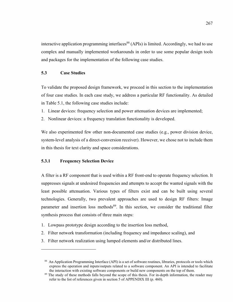
267
interactive application programming interfaces88 (APIs) is limited. Accordingly, we had to use
complex and manually implemented workarounds in order to use some popular design tools
and packages for the implementation of the following case studies.
5.3 Case Studies
To validate the proposed design framework, we proceed in this section to the implementation
of four case studies. In each case study, we address a particular RF functionality. As detailed
in Table 5.1, the following case studies include:
1. Linear devices: frequency selection and power attenuation devices are implemented;
2. Nonlinear devices: a frequency translation functionality is developed.
We also experimented few other non-documented case studies (e.g., power division device,
system-level analysis of a direct-conversion receiver). However, we chose not to include them
in this thesis for text clarity and space considerations.
5.3.1 Frequency Selection Device
A filter is a RF component that is used within a RF front-end to operate frequency selection. It
suppresses signals at undesired frequencies and attempts to accept the wanted signals with the
least possible attenuation. Various types of filters exist and can be built using several
technologies. Generally, two prevalent approaches are used to design RF filters: Image
parameter and insertion loss methods89. In this section, we consider the traditional filter
synthesis process that consists of three main steps:
1. Lowpass prototype design according to the insertion loss method,
2. Filter network transformation (including frequency and impedance scaling), and
3. Filter network realization using lumped elements and/or distributed lines.
88 An Application Programming Interface (API) is a set of software routines, libraries, protocols or tools which express the operation and inputs/outputs related to a software component. An API is intended to facilitate the interaction with existing software components or build new components on the top of them.
89 The study of these methods falls beyond the scope of this thesis. For in-depth information, the reader may refer to the list of references given in section 5 of APPENDIX III (p. 460).
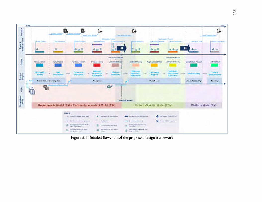
Figure 5.1 Detailed flowchart of the proposed design framework
268
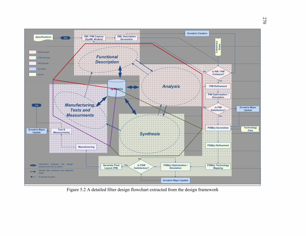
269
Q-Matrix
Functional Description
Analysis
Synthesis
Manufacturing, Tests and
Measurments
startSpecifications RM / PIM Capture(SysML Models)
XML Description Generation
PIM Refinement
Yes
No
Q-matrix Creation
PIM Optimization / Simulation
Yes
No
Technology Data
Q-matrix Major Update
is PIM Satisfactory?
PSM(s) Refinement
PSM(s) Technology Mapping
PSM(s) Optimization / Simulation
YesGenerate Final Layout (PM)
Manufacturing
Test & Measurements
is PSM Satisfactory?
No
Q-matrix Major Update
Q-matrix Major Update
Co
her
enc
e R
ule
s
PSM(s) Generation
end
is RM / PIM Coherent?
PIM Domain
PSM Domain
PM Domain
Q-matrix
Interaction between the design scheme and the Q-matrix
Design flow between two adjacent steps
Eventual re-spins
Inputs
Figure 5.2 A detailed filter design flowchart extracted from the design framework
270
270
Table 5.1 List of case studies
Case Study Objective PSM Abstraction
Level PM Target Technology
Q-matrix
RF Bandpass Filter
Presentation of a step-by-step tutorial demonstrating the major aspects of the framework including:
− Functional description − Coherence verification − System-level analyses − Model-to-model transformation − Granularity change − Automated decision making − Automated technology mapping
Circuit LC/Microstrip Q-matrix creation and evolution throughout the design cycle
RF Lowpass Filter Presentation of the framework’s capability of using multiple PIM-to-PSM transformations in order to create many PSMs from the PIM
Circuit Microstrip Q-matrix support for noise data
RF Attenuator Presentation of the framework’s concurrent design capability
Circuit LC/Microstrip Q-matrix support for concurrent design data
RF Passive Mixer Summary of a passive mixer design using the design framework from two design perspectives
Circuit / Module PSM only Q-matrix support for nonlinear design data
269
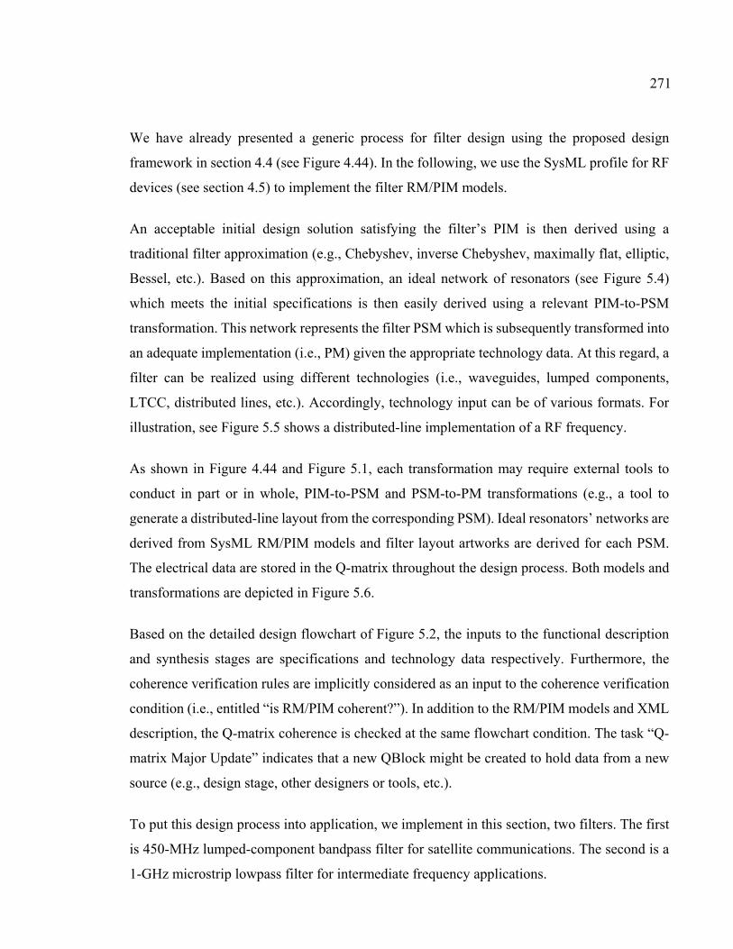
We have already presented a generic process for filter design using the proposed design
framework in section 4.4 (see Figure 4.44). In the following, we use the SysML profile for RF
devices (see section 4.5) to implement the filter RM/PIM models.
An acceptable initial design solution satisfying the filter’s PIM is then derived using a
traditional filter approximation (e.g., Chebyshev, inverse Chebyshev, maximally flat, elliptic,
Bessel, etc.). Based on this approximation, an ideal network of resonators (see Figure 5.4)
which meets the initial specifications is then easily derived using a relevant PIM-to-PSM
transformation. This network represents the filter PSM which is subsequently transformed into
an adequate implementation (i.e., PM) given the appropriate technology data. At this regard, a
filter can be realized using different technologies (i.e., waveguides, lumped components,
LTCC, distributed lines, etc.). Accordingly, technology input can be of various formats. For
illustration, see Figure 5.5 shows a distributed-line implementation of a RF frequency.
As shown in Figure 4.44 and Figure 5.1, each transformation may require external tools to
conduct in part or in whole, PIM-to-PSM and PSM-to-PM transformations (e.g., a tool to
generate a distributed-line layout from the corresponding PSM). Ideal resonators’ networks are
derived from SysML RM/PIM models and filter layout artworks are derived for each PSM.
The electrical data are stored in the Q-matrix throughout the design process. Both models and
transformations are depicted in Figure 5.6.
Based on the detailed design flowchart of Figure 5.2, the inputs to the functional description
and synthesis stages are specifications and technology data respectively. Furthermore, the
coherence verification rules are implicitly considered as an input to the coherence verification
condition (i.e., entitled “is RM/PIM coherent?”). In addition to the RM/PIM models and XML
description, the Q-matrix coherence is checked at the same flowchart condition. The task “Q-
matrix Major Update” indicates that a new QBlock might be created to hold data from a new
source (e.g., design stage, other designers or tools, etc.).
To put this design process into application, we implement in this section, two filters. The first
is 450-MHz lumped-component bandpass filter for satellite communications. The second is a
1-GHz microstrip lowpass filter for intermediate frequency applications.
271
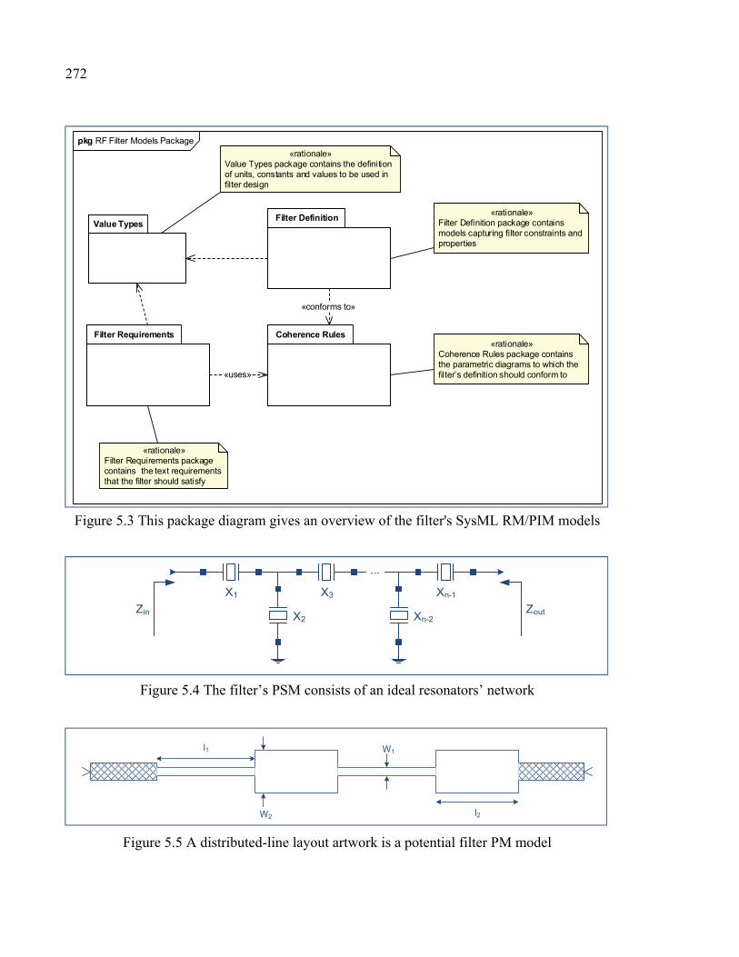
272
Value Types
pkg RF Filter Models Package
«rationale»Filter Definition package contains models capturing filter constraints and properties
Filter Definition
Filter Requirements
«rationale»Filter Requirements package contains the text requirements that the filter should satisfy
«rationale»Value Types package contains the definition of units, constants and values to be used in filter design
«rationale»Coherence Rules package contains the parametric diagrams to which the filter’s definition should conform to
Coherence Rules
«conforms to»
«uses»
Figure 5.3 This package diagram gives an overview of the filter's SysML RM/PIM models
...
Zin Zout
X1 X3 Xn-1
X2 Xn-2
Figure 5.4 The filter’s PSM consists of an ideal resonators’ network
l1
W2 l2
W1
Figure 5.5 A distributed-line layout artwork is a potential filter PM model
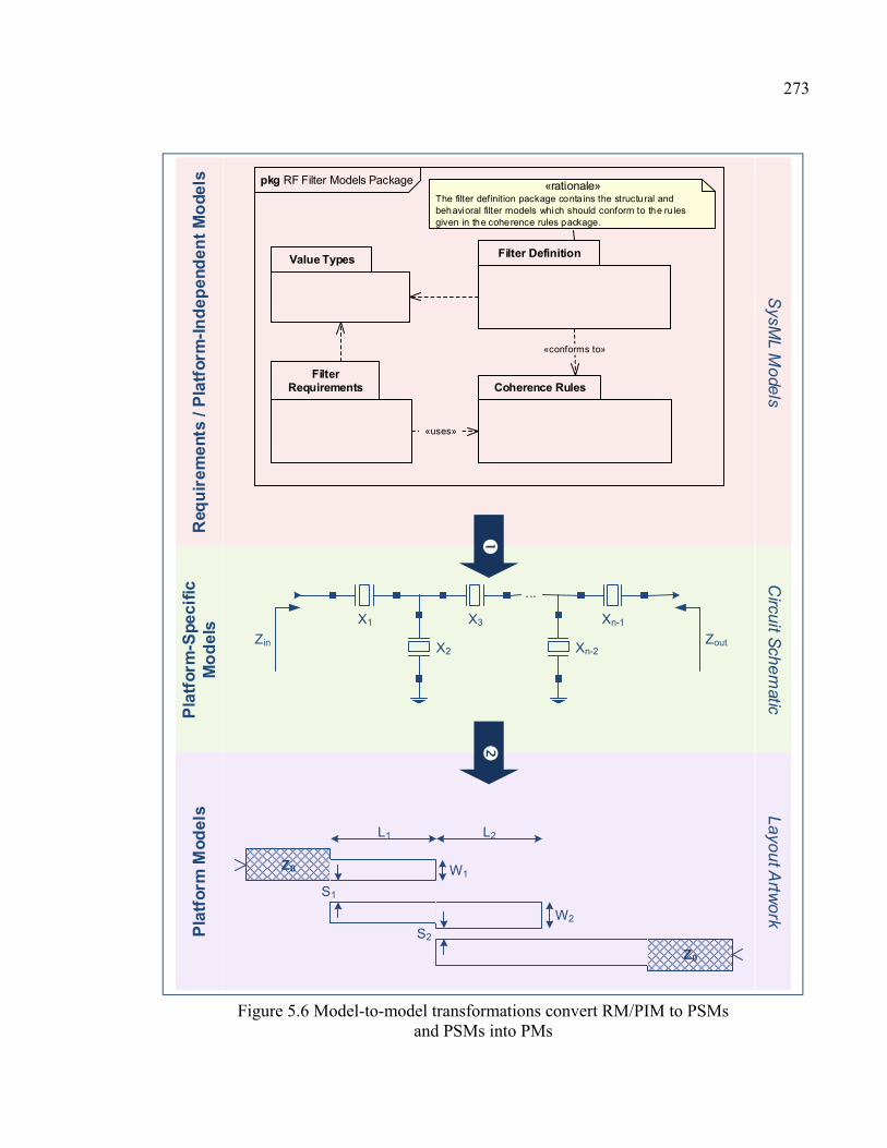
273
Value Types
pkg RF Filter Models Package
Filter Definition
Filter Requirements
«rationale»The filter definition package conta ins the structural and behavioral filter models which should conform to the ru les given in the coherence rules package.
L1 L2
W1
W2
S1
S2
Z0
Z0
Req
uir
em
en
ts /
Pla
tfo
rm-I
nd
ep
en
de
nt
Mo
del
sP
latf
orm
-Sp
ecif
ic
Mo
del
sP
latf
orm
Mo
del
s Layou
t Artw
ork
Circuit S
che
matic
SysM
L Mo
dels
...
Zin Zout
X1 X3 Xn-1
X2 Xn-2
Coherence Rules
«conforms to»
«uses»
Figure 5.6 Model-to-model transformations convert RM/PIM to PSMs and PSMs into PMs
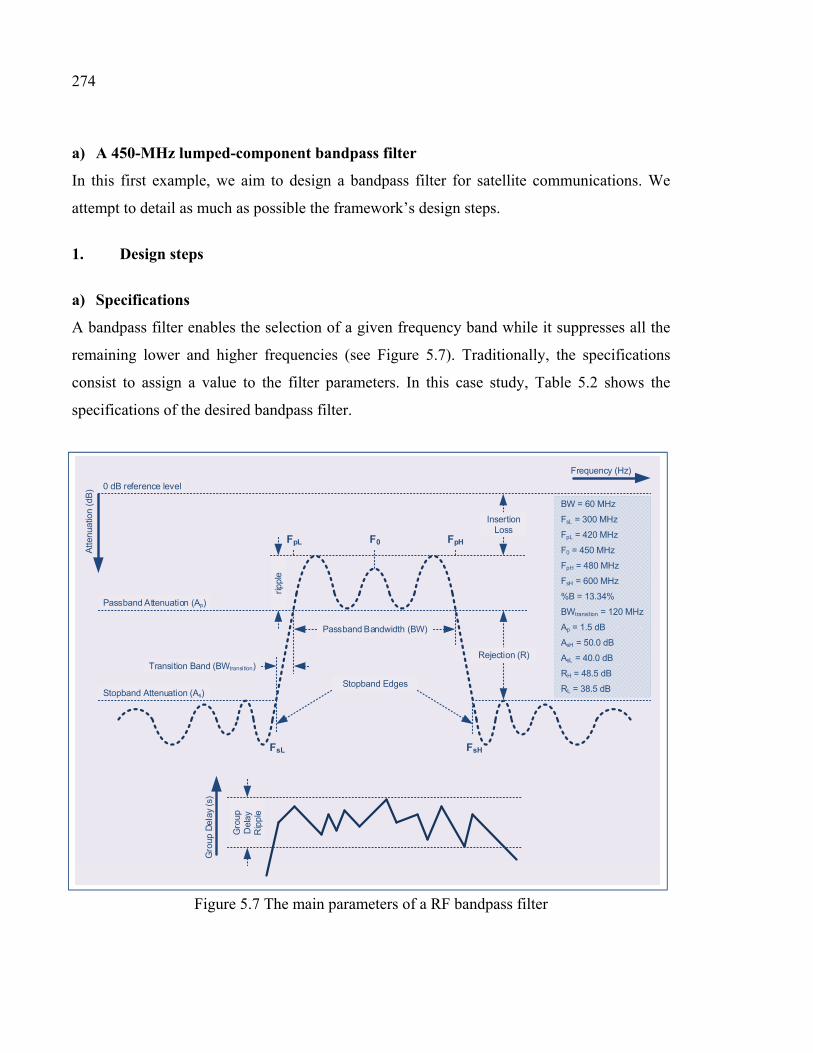
274
a) A 450-MHz lumped-component bandpass filter
In this first example, we aim to design a bandpass filter for satellite communications. We
attempt to detail as much as possible the framework’s design steps.
1. Design steps
a) Specifications
A bandpass filter enables the selection of a given frequency band while it suppresses all the
remaining lower and higher frequencies (see Figure 5.7). Traditionally, the specifications
consist to assign a value to the filter parameters. In this case study, Table 5.2 shows the
specifications of the desired bandpass filter.
Gro
up
Del
ay
Rip
ple
Stopband Attenuation (As)
Passband Attenuation (Ap)
0 dB reference level
rippl
e
F0
Insertion Loss
Rejection (R)
Passband Bandwidth (BW)
Stopband Edges
FsL FsH
FpL FpH
Transition Band (BWtransition)
Atte
nuat
ion
(dB
)
Frequency (Hz)
BW = 60 MHz
FsL = 300 MHz
FpL = 420 MHz
F0 = 450 MHz
FpH = 480 MHz
FsH = 600 MHz
%B = 13.34%
BWtransition = 120 MHz
Ap = 1.5 dB
AsH = 50.0 dB
AsL = 40.0 dB
RH = 48.5 dB
Gro
up D
elay
(s)
RL = 38.5 dB
Figure 5.7 The main parameters of a RF bandpass filter
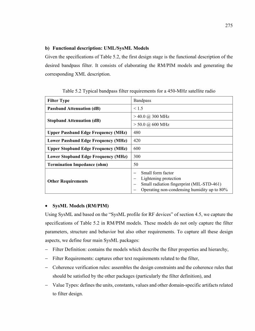
275
b) Functional description: UML/SysML Models
Given the specifications of Table 5.2, the first design stage is the functional description of the
desired bandpass filter. It consists of elaborating the RM/PIM models and generating the
corresponding XML description.
Table 5.2 Typical bandpass filter requirements for a 450-MHz satellite radio
Filter Type Bandpass
Passband Attenuation (dB) < 1.5
Stopband Attenuation (dB) > 40.0 @ 300 MHz
> 50.0 @ 600 MHz
Upper Passband Edge Frequency (MHz) 480
Lower Passband Edge Frequency (MHz) 420
Upper Stopband Edge Frequency (MHz) 600
Lower Stopband Edge Frequency (MHz) 300
Termination Impedance (ohm) 50
Other Requirements
− Small form factor − Lightening protection − Small radiation fingerprint (MIL-STD-461) − Operating non-condensing humidity up to 80%
• SysML Models (RM/PIM)
Using SysML and based on the “SysML profile for RF devices” of section 4.5, we capture the
specifications of Table 5.2 in RM/PIM models. These models do not only capture the filter
parameters, structure and behavior but also other requirements. To capture all these design
aspects, we define four main SysML packages:
− Filter Definition: contains the models which describe the filter properties and hierarchy,
− Filter Requirements: captures other text requirements related to the filter,
− Coherence verification rules: assembles the design constraints and the coherence rules that
should be satisfied by the other packages (particularly the filter definition), and
− Value Types: defines the units, constants, values and other domain-specific artifacts related
to filter design.
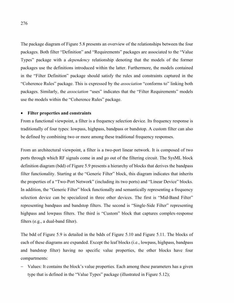
276
The package diagram of Figure 5.8 presents an overview of the relationships between the four
packages. Both filter “Definition” and “Requirements” packages are associated to the “Value
Types” package with a dependency relationship denoting that the models of the former
packages use the definitions introduced within the latter. Furthermore, the models contained
in the “Filter Definition” package should satisfy the rules and constraints captured in the
“Coherence Rules” package. This is expressed by the association “conforms to” linking both
packages. Similarly, the association “uses” indicates that the “Filter Requirements” models
use the models within the “Coherence Rules” package.
• Filter properties and constraints
From a functional viewpoint, a filter is a frequency selection device. Its frequency response is
traditionally of four types: lowpass, highpass, bandpass or bandstop. A custom filter can also
be defined by combining two or more among these traditional frequency responses.
From an architectural viewpoint, a filter is a two-port linear network. It is composed of two
ports through which RF signals come in and go out of the filtering circuit. The SysML block
definition diagram (bdd) of Figure 5.9 presents a hierarchy of blocks that derives the bandpass
filter functionality. Starting at the “Generic Filter” block, this diagram indicates that inherits
the properties of a “Two-Port Network” (including its two ports) and “Linear Device” blocks.
In addition, the “Generic Filter” block functionally and semantically representing a frequency
selection device can be specialized in three other devices. The first is “Mid-Band Filter”
representing bandpass and bandstop filters. The second is “Single-Side Filter” representing
highpass and lowpass filters. The third is “Custom” block that captures complex-response
filters (e.g., a dual-band filter).
The bdd of Figure 5.9 is detailed in the bdds of Figure 5.10 and Figure 5.11. The blocks of
each of these diagrams are expanded. Except the leaf blocks (i.e., lowpass, highpass, bandpass
and bandstop filter) having no specific value properties, the other blocks have four
compartments:
− Values: It contains the block’s value properties. Each among these parameters has a given
type that is defined in the “Value Types” package (illustrated in Figure 5.12);
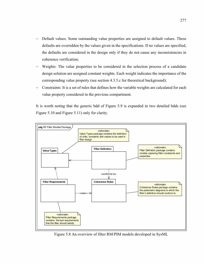
277
− Default values: Some outstanding value properties are assigned to default values. These
defaults are overridden by the values given in the specifications. If no values are specified,
the defaults are considered in the design only if they do not cause any inconsistencies in
coherence verification;
− Weights: The value properties to be considered in the selection process of a candidate
design solution are assigned constant weights. Each weight indicates the importance of the
corresponding value property (see section 4.3.5.c for theoretical background);
− Constraints: It is a set of rules that defines how the variable weights are calculated for each
value property considered in the previous compartment.
It is worth noting that the generic bdd of Figure 5.9 is expanded in two detailed bdds (see
Figure 5.10 and Figure 5.11) only for clarity.
Value Types
pkg RF Filter Models Package
«rationale»Filter Definition package contains models capturing filter constraints and properties
Filter Definition
Filter Requirements
«rationale»Filter Requirements package contains the text requirements that the filter should satisfy
«rationale»Value Types package contains the definition of units, constants and values to be used in filter design
«rationale»Coherence Rules package contains the parametric diagrams to which the filter’s definition should conform to
Coherence Rules
«conforms to»
«uses»
Figure 5.8 An overview of filter RM/PIM models developed in SysML
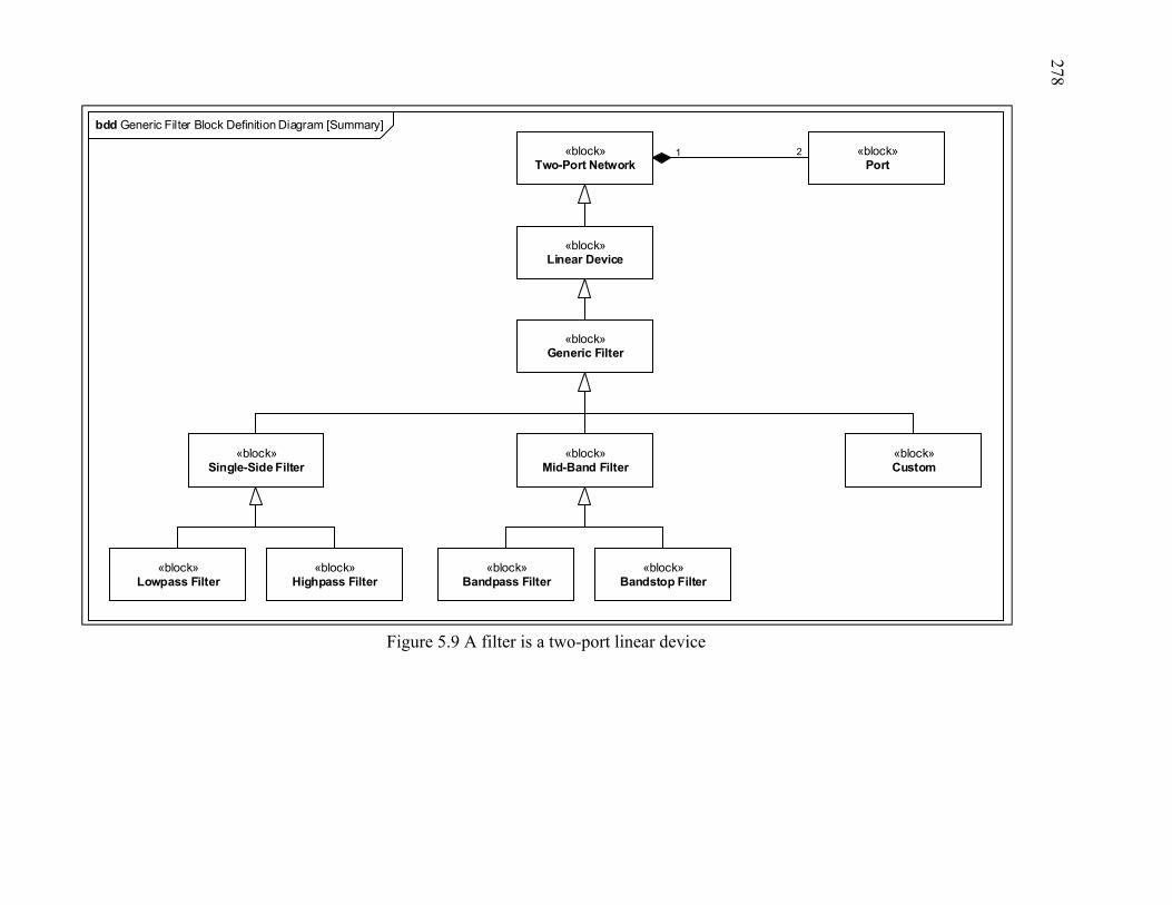
bdd Generic Filter Block Definition Diagram [Summary]
«block»Bandpass Filter
«block»Bandstop Filter
«block»Highpass Filter
«block»Lowpass Filter
1 2«block»Two-Port Network
«block»Port
«block»Generic Filter
«block»Mid-Band Filter
«block»Single-Side Filter
«block»Custom
«block»Linear Device
Figure 5.9 A filter is a two-port linear device
278
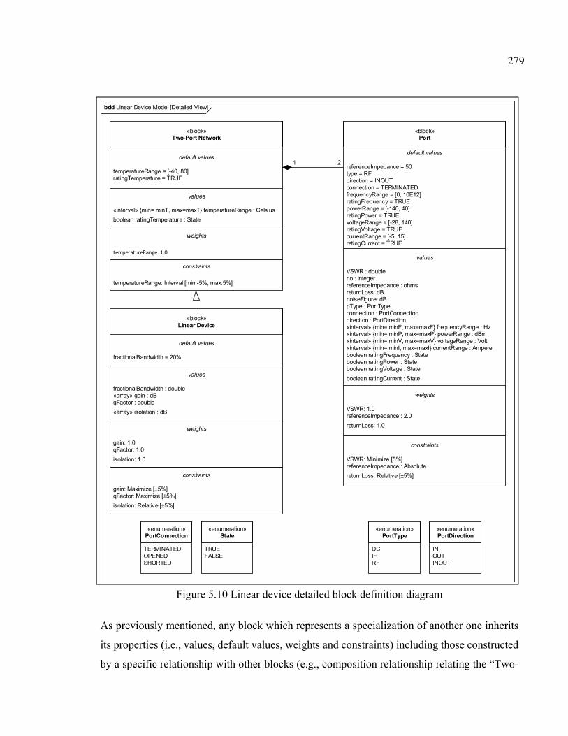
bdd Linear Device Model [Detailed View]
«block»Two-Port Network
default values
temperatureRange = [-40, 80]ratingTemperature = TRUE
«block»Port
values
«interval» min= minT, max=maxT temperatureRange : Celsius
boolean ratingTemperature : State
weights
temperatureRange: 1.0
1 2
default values
referenceImpedance = 50type = RFdirection = INOUTconnection = TERMINATEDfrequencyRange = [0, 10E12]ratingFrequency = TRUEpowerRange = [-140, 40]ratingPower = TRUEvoltageRange = [-28, 140]ratingVoltage = TRUEcurrentRange = [-5, 15]ratingCurrent = TRUE
values
VSWR : doubleno : integerreferenceImpedance : ohmsreturnLoss: dBnoiseFigure: dBpType : PortTypeconnection : PortConnectiondirection : PortDirection«interval» min= minF, max=maxF frequencyRange : Hz«interval» min= minP, max=maxP powerRange : dBm«interval» min= minV, max=maxV voltageRange : Volt«interval» min= minI, max=maxI currentRange : Ampereboolean ratingFrequency : Stateboolean ratingPower : Stateboolean ratingVoltage : State
boolean ratingCurrent : State
weights
VSWR: 1.0referenceImpedance : 2.0
returnLoss: 1.0
default values
fractionalBandwidth = 20%
values
fractionalBandwidth : double«array» gain : dBqFactor : double
«array» isolation : dB
weights
gain: 1.0qFactor: 1.0
isolation: 1.0
constraints
VSWR: Minimize [5%]referenceImpedance : Absolute
returnLoss: Relative [±5%]constraints
gain: Maximize [±5%]qFactor: Maximize [±5%]
isolation: Relative [±5%]
constraints
temperatureRange: Interval [min:-5%, max:5%]
«enumeration»PortType
DCIFRF
«enumeration»PortDirection
INOUTINOUT
«enumeration»State
TRUEFALSE
«enumeration»PortConnection
TERMINATEDOPENEDSHORTED
«block»Linear Device
Figure 5.10 Linear device detailed block definition diagram
As previously mentioned, any block which represents a specialization of another one inherits
its properties (i.e., values, default values, weights and constraints) including those constructed
by a specific relationship with other blocks (e.g., composition relationship relating the “Two-
279
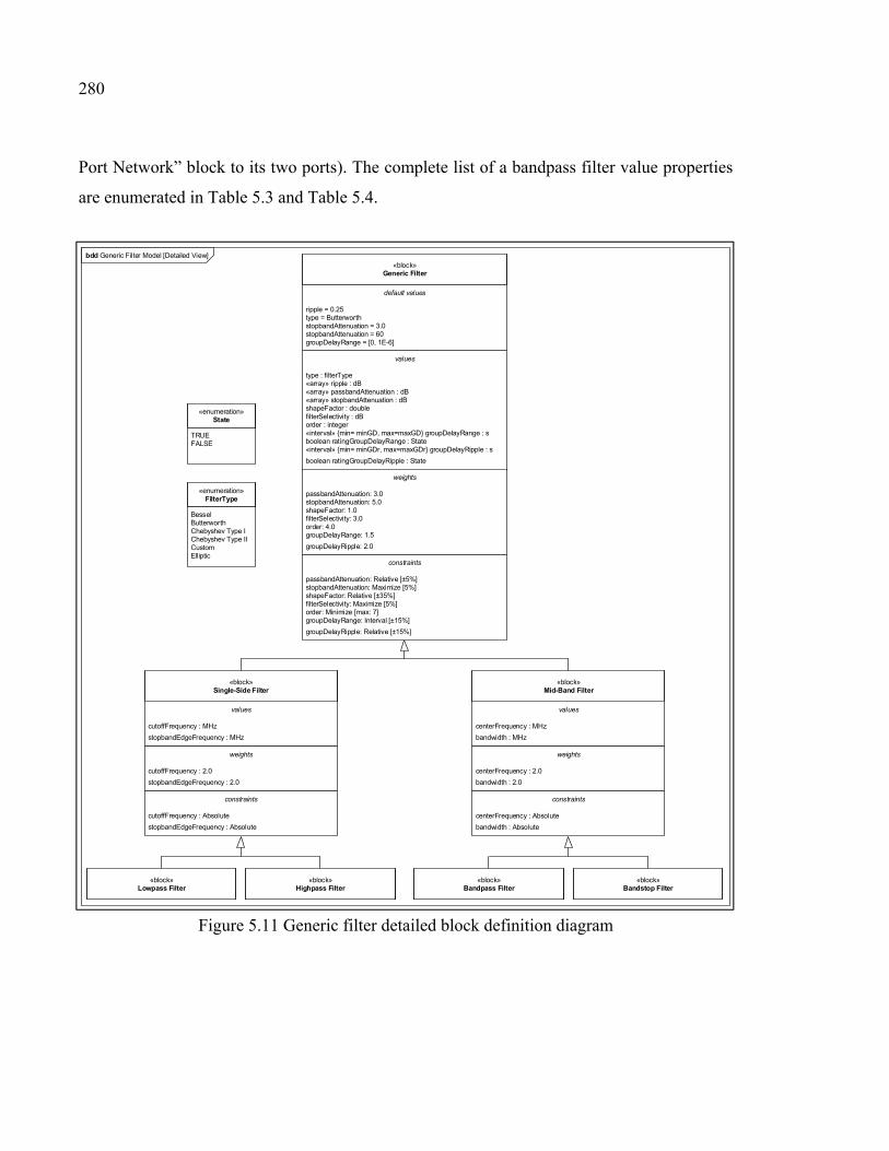
280
Port Network” block to its two ports). The complete list of a bandpass filter value properties
are enumerated in Table 5.3 and Table 5.4.
bdd Generic Filter Model [Detailed View]«block»
Generic Filter
«enumeration»FilterType
default values
ripple = 0.25type = ButterworthstopbandAttenuation = 3.0stopbandAttenuation = 60groupDelayRange = [0, 1E-6]
«enumeration»State
BesselButterworthChebyshev Type IChebyshev Type IICustomElliptic
TRUEFALSE
values
type : filterType«array» ripple : dB«array» passbandAttenuation : dB«array» stopbandAttenuation : dBshapeFactor : doublefilterSelectivity : dBorder : integer«interval» min= minGD, max=maxGD groupDelayRange : sboolean ratingGroupDelayRange : State«interval» min= minGDr, max=maxGDr groupDelayRipple : s
boolean ratingGroupDelayRipple : State
weights
passbandAttenuation: 3.0stopbandAttenuation: 5.0shapeFactor: 1.0filterSelectivity: 3.0order: 4.0groupDelayRange: 1.5
groupDelayRipple: 2.0
values
cutoffFrequency : MHz
stopbandEdgeFrequency : MHz
values
centerFrequency : MHz
bandwidth : MHz
«block»Lowpass Filter
«block»Highpass Filter
«block»Single-Side Filter
«block»Mid-Band Filter
«block»Bandpass Filter
«block»Bandstop Filter
weights
cutoffFrequency : 2.0
stopbandEdgeFrequency : 2.0
weights
centerFrequency : 2.0
bandwidth : 2.0
constraints
passbandAttenuation: Relative [±5%]stopbandAttenuation: Maximize [5%]shapeFactor: Relative [±35%]filterSelectivity: Maximize [5%]order: Minimize [max: 7]groupDelayRange: Interval [±15%]
groupDelayRipple: Relative [±15%]
constraints
cutoffFrequency : Absolute
stopbandEdgeFrequency : Absolute
constraints
centerFrequency : Absolute
bandwidth : Absolute
Figure 5.11 Generic filter detailed block definition diagram
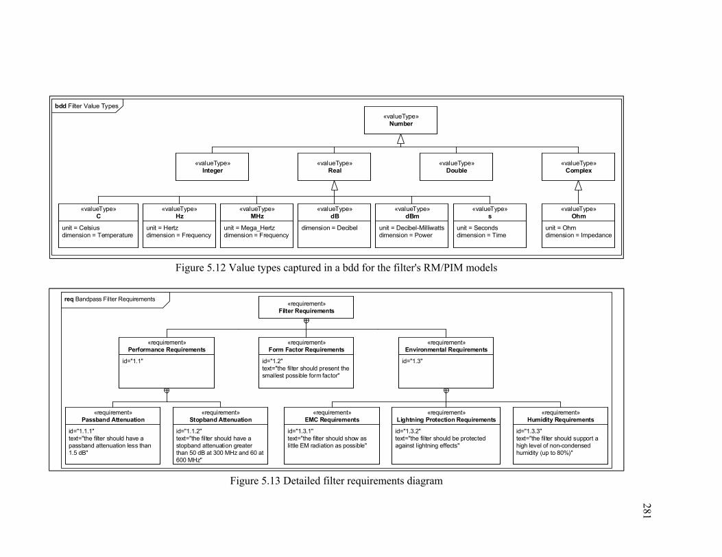
bdd Filter Value Types
«valueType»Real
unit = Hertzdimension = Frequency
«valueType»Hz
unit = Mega_Hertzdimension = Frequency
«valueType»MHz
dimension = Decibel
«valueType»dB
unit = Decibel-Milliwattsdimension = Power
«valueType»dBm
unit = Secondsdimension = Time
«valueType»s
«valueType»Double
«valueType»Integer
«valueType»Complex
«valueType»Number
unit = Ohmdimension = Impedance
«valueType»Ohm
unit = Celsiusdimension = Temperature
«valueType»C
Figure 5.12 Value types captured in a bdd for the filter's RM/PIM models
req Bandpass Filter Requirements
«requirement»Filter Requirements
id="1.2"text="the filter should present the smallest possible form factor"
«requirement»Form Factor Requirements
id="1.3"
«requirement»Environmental Requirements
id="1.3.1"text="the filter should show as little EM radiation as possible"
«requirement»EMC Requirements
id="1.3.2"text="the filter should be protected against lightning effects"
«requirement»Lightning Protection Requirements
id="1.3.3"text="the filter should support a high level of non-condensed humidity (up to 80%)"
«requirement»Humidity Requirements
id="1.1"
«requirement»Performance Requirements
id="1.1.1"text="the filter should have a passband attenuation less than 1.5 dB"
«requirement»Passband Attenuation
id="1.1.2"text="the filter should have a stopband attenuation greater than 50 dB at 300 MHz and 60 at 600 MHz"
«requirement»Stopband Attenuation
Figure 5.13 Detailed filter requirements diagram
281
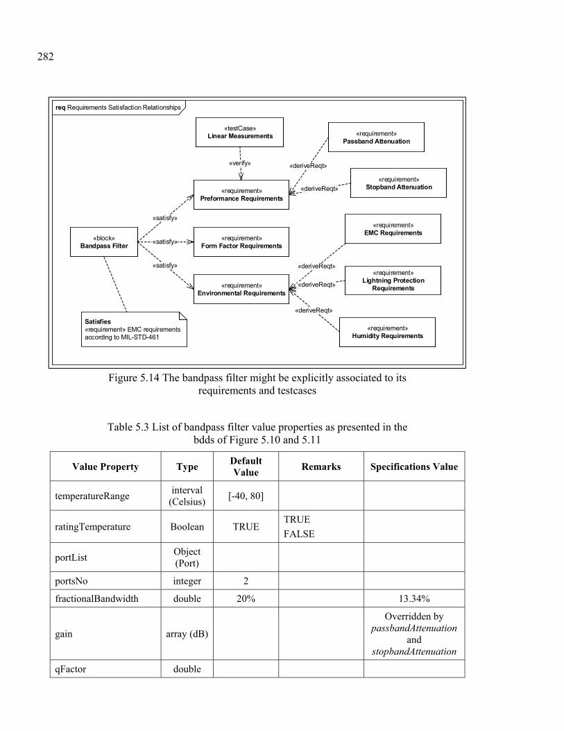
req Requirements Satisfaction Relationships
«satisfy»
«block»Bandpass Filter
«requirement»Preformance Requirements
«requirement»Form Factor Requirements
«satisfy»
«requirement»Environmental Requirements
«satisfy»
«testCase»Linear Measurements
«verify»
Satisfies«requirement» EMC requirements according to MIL-STD-461
«requirement»Lightning Protection
Requirements
«requirement»EMC Requirements
«requirement»Humidity Requirements
«deriveReqt»
«deriveReqt»
«deriveReqt»
«requirement»Passband Attenuation
«deriveReqt»
«requirement»Stopband Attenuation«deriveReqt»
Figure 5.14 The bandpass filter might be explicitly associated to its requirements and testcases
Table 5.3 List of bandpass filter value properties as presented in the bdds of Figure 5.10 and 5.11
Value Property Type Default Value
Remarks Specifications Value
temperatureRange interval
(Celsius) [-40, 80]
ratingTemperature Boolean TRUE TRUE
FALSE
portList Object (Port)
portsNo integer 2
fractionalBandwidth double 20% 13.34%
gain array (dB)
Overridden by passbandAttenuation
and stopbandAttenuation
qFactor double
282
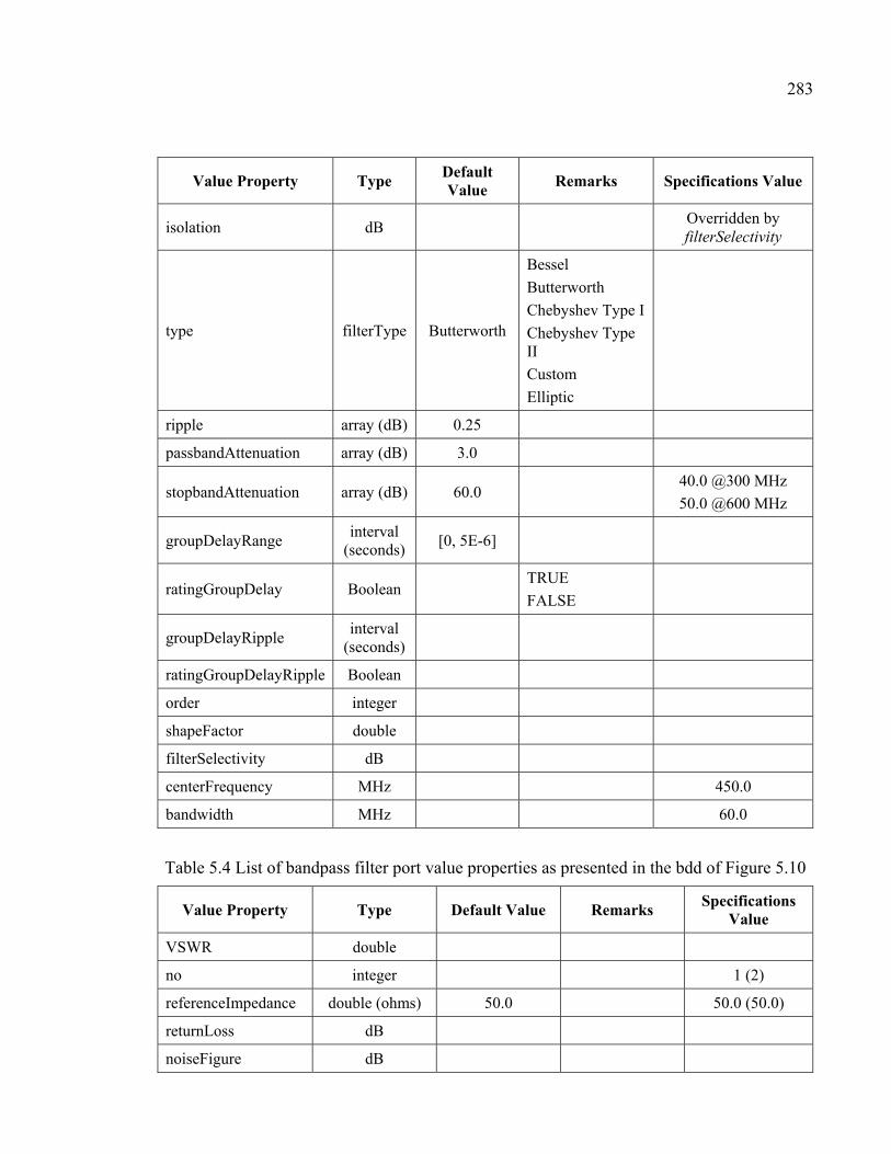
283
Value Property Type Default Value
Remarks Specifications Value
isolation dB Overridden by filterSelectivity
type filterType Butterworth
Bessel
Butterworth
Chebyshev Type I
Chebyshev Type II
Custom
Elliptic
ripple array (dB) 0.25
passbandAttenuation array (dB) 3.0
stopbandAttenuation array (dB) 60.0 40.0 @300 MHz
50.0 @600 MHz
groupDelayRange interval
(seconds) [0, 5E-6]
ratingGroupDelay Boolean TRUE
FALSE
groupDelayRipple interval
(seconds)
ratingGroupDelayRipple Boolean
order integer
shapeFactor double
filterSelectivity dB
centerFrequency MHz 450.0
bandwidth MHz 60.0
Table 5.4 List of bandpass filter port value properties as presented in the bdd of Figure 5.10
Value Property Type Default Value Remarks Specifications
Value
VSWR double
no integer 1 (2)
referenceImpedance double (ohms) 50.0 50.0 (50.0)
returnLoss dB
noiseFigure dB
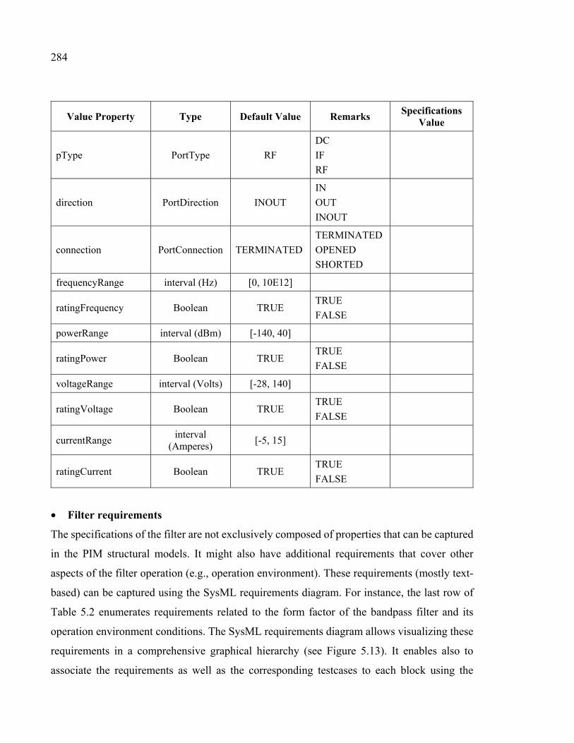
284
Value Property Type Default Value Remarks Specifications
Value
pType PortType RF
DC
IF
RF
direction PortDirection INOUT
IN
OUT
INOUT
connection PortConnection TERMINATED
TERMINATED
OPENED
SHORTED
frequencyRange interval (Hz) [0, 10E12]
ratingFrequency Boolean TRUE TRUE
FALSE
powerRange interval (dBm) [-140, 40]
ratingPower Boolean TRUE TRUE
FALSE
voltageRange interval (Volts) [-28, 140]
ratingVoltage Boolean TRUE TRUE
FALSE
currentRange interval
(Amperes) [-5, 15]
ratingCurrent Boolean TRUE TRUE
FALSE
• Filter requirements
The specifications of the filter are not exclusively composed of properties that can be captured
in the PIM structural models. It might also have additional requirements that cover other
aspects of the filter operation (e.g., operation environment). These requirements (mostly text-
based) can be captured using the SysML requirements diagram. For instance, the last row of
Table 5.2 enumerates requirements related to the form factor of the bandpass filter and its
operation environment conditions. The SysML requirements diagram allows visualizing these
requirements in a comprehensive graphical hierarchy (see Figure 5.13). It enables also to
associate the requirements as well as the corresponding testcases to each block using the
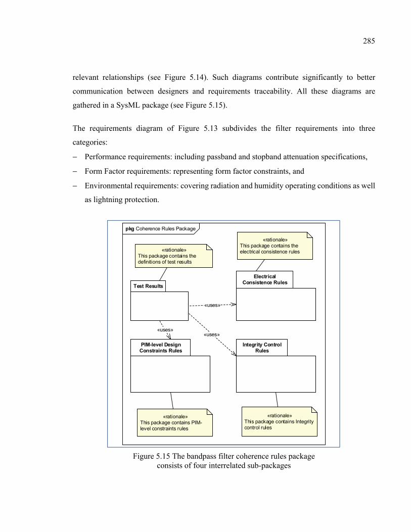
285
relevant relationships (see Figure 5.14). Such diagrams contribute significantly to better
communication between designers and requirements traceability. All these diagrams are
gathered in a SysML package (see Figure 5.15).
The requirements diagram of Figure 5.13 subdivides the filter requirements into three
categories:
− Performance requirements: including passband and stopband attenuation specifications,
− Form Factor requirements: representing form factor constraints, and
− Environmental requirements: covering radiation and humidity operating conditions as well
as lightning protection.
Test Results
pkg Coherence Rules Package
«rationale»This package contains the electrical consistence rules
Electrical Consistence Rules
PIM-level Design Constraints Rules
«uses»
«uses»
«rationale»This package contains PIM-level constraints rules
«rationale»This package contains the definitions of test results
«rationale»This package contains Integrity control rules
Integrity Control Rules
«uses»
Figure 5.15 The bandpass filter coherence rules package consists of four interrelated sub-packages
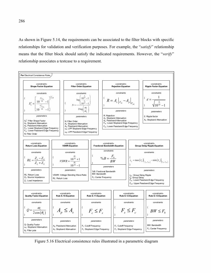
286
As shown in Figure 5.14, the requirements can be associated to the filter blocks with specific
relationships for validation and verification purposes. For example, the “satisfy” relationship
means that the filter block should satisfy the indicated requirements. However, the “verify”
relationship associates a testcase to a requirement.
Par Electrical Consistence Rules
«constraint»Rule E.13:Equation
constraints
0BW F≤
parameters
BW: Bandwidth
F0: Center Frequency
«constraint»Rule E.10:Equation
constraints
p sA A≤
parameters
Ap: Passband Attenuation
As: Stopband Attenuation
«constraint»Rule E.11:Equation
constraints
c sF F≤
parameters
Fc: Cutoff Frequency
Fs: Stopband Edge Frequency
«constraint»Rule E.12:Equation
constraints
s cF F≤
parameters
Fc: Cutoff Frequency
Fs: Stopband Edge Frequency
«constraint»Group Delay Ripple:Equation
constraints
parameters
rζg : Group Delay Rippleζg: Group DelayFpL: Lower Passband Edge Frequency
FpH: Upper Passband Edge Frequency
( ) ( ), ,
max ming
pL pH pL pHg g
F F F Frτ τ τ
= −
«constraint»Rejection:Equation
constraints
sL
pLs F p F
R A A= −
parameters
R: RejectionAs: Stopband AttenuationAp: Passband AttenuationFsL: Lower Stopband Edge Frequency
FpL: Lower Passband Edge Frequency
«constraint»Shape Factor:Equation
constraints
parameters
Sab: Filter Shape Factor
As: Stopband AttenuationAp: Passband AttenuationFsL: Lower Stopband Edge FrequencyFpL: Lower Passband Edge Frequency
N: Filter Order
12
10
10
10 1
10 1
s FsL
p FpL
NA
ba A
S
−=
−
«constraint»Return Loss:Equation
constraints
L S
L S
Z ZRL
Z Z
−=+
parameters
RL: Return LossZS: Source Impedance
ZL: Load Impedance
«constraint»VSWR:Equation
constraints
20
20
10 1
10 1
RL
RLVSWR+=−
parameters
VSWR: Voltage Standing Wave Ratio
RL: Return Loss
«constraint»Ripple Factor:Equation
constraints
parameters
Ɛ: Ripple factor
As: Stopband Attenuation
10
1
10 1sA
ε =
−
«constraint»Quality Factor:Equation
constraints
( )2cosc
k
Qω
θ=
parameters
Q: Quality Factorωc: Stopband Attenuation
θk: Filter pole
«constraint»Filter Order:Equation
constraints
parameters
N: Filter OrderAs: Stopband AttenuationAp: Passband Attenuationωs: LPP Stopband Edge Frequency
ωp: LPP Passband Edge Frequency
10
10
10 1log
10 1
2log
s
p
A
A
s
p
Nωω
−
− =
«constraint»Fractional Bandwidth:Equation
constraints
parameters
%B: Fractional BandwidthBW: Bandwidth
F0: Center Frequency
0%F
BBW
=
Figure 5.16 Electrical consistence rules illustrated in a parametric diagram
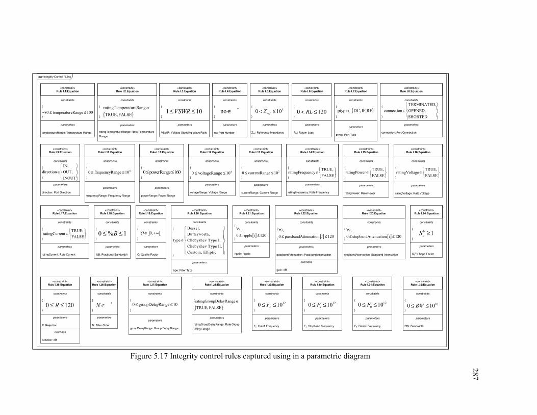
par Integrity Control Rules
«constraint»Rule I.1:Equation
constraints
parameters
temperatureRange: Temperature Range
80 temperatureRange 100− ≤ ≤
«constraint»Rule I.2:Equation
constraints
ratingTemperatureRange
TRUE,FALSE
∈
parameters
ratingTemperatureRange: Rate Temperature
Range
«constraint»Rule I.3:Equation
constraints
parameters
VSWR: Voltage Standing Wave Ratio
1 10VSWR≤ ≤
«constraint»Rule I.4:Equation
constraints
*no ∈
parameters
no: Port Number
«constraint»Rule I.5:Equation
constraints
parameters
Zref: Reference Impedance
410refZ0 < ≤
«constraint»Rule I.6:Equation
constraints
parameters
RL: Return Loss
120RL0 < ≤
«constraint»Rule I.7:Equation
constraints
ptype DC, IF,RF∈
parameters
ptype: Port Type
«constraint»Rule I.8:Equation
constraints
TERMINATED,
connection OPENED,
SHORTED
∈
parameters
connection: Port Connection
«constraint»Rule I.10:Equation
constraints
120 frequencyRange 10≤ ≤
parameters
frequencyRange: Frequency Range
«constraint»Rule I.9:Equation
constraints
IN,
direction OUT,
INOUT
∈
parameters
direction: Port Direction
«constraint»Rule I.11:Equation
constraints
parameters
powerRange: Power Range
0 powerRange 160≤ ≤
«constraint»Rule I.12:Equation
constraints
parameters
voltageRange: Voltage Range
40 voltageRange 10≤ ≤
«constraint»Rule I.14:Equation
constraints
TRUE,ratingFrequency
FALSE
∈
parameters
ratingFrequency: Rate Frequency
«constraint»Rule I.13:Equation
constraints
parameters
currentRange: Current Range
20 currentRange 10≤ ≤
«constraint»Rule I.19:Equation
constraints
] [0,Q ∈ +∞
parameters
Q: Quality Factor
«constraint»Rule I.18:Equation
constraints
0 % 1B≤ ≤
parameters
%B: Fractional Bandwidth
«constraint»Rule I.17:Equation
constraints
TRUE,ratingCurrent
FALSE
∈
parameters
ratingCurrent: Rate Current
«constraint»Rule I.16:Equation
constraints
TRUE,ratingVoltage
FALSE
∈
parameters
ratingVoltage: Rate Voltage
«constraint»Rule I.15:Equation
constraints
TRUE,ratingPower
FALSE
∈
parameters
ratingPower: Rate Power
«constraint»Rule I.22:Equation
constraints
[ ]
,
0 passbandAttenuation 120
i
i
∀≤ ≤
parameters
passbandAttenuation: Passband Attenuation
overrides
gain: dB
«constraint»Rule I.23:Equation
constraints
[ ]
,
0 stopbandAttenuation 120
i
i
∀≤ ≤
parameters
stopbandAttenuation: Stopband Attenuation
«constraint»Rule I.24:Equation
constraints
1baS ≥
parameters
Sab: Shape Factor
«constraint»Rule I.25:Equation
constraints
0 120R≤ ≤
parameters
R: Rejection
overrides
isolation: dB
«constraint»Rule I.26:Equation
constraints
*N ∈
parameters
N: Filter Order
«constraint»Rule I.27:Equation
constraints
0 groupDelayRange 10≤ ≤
parameters
groupDelayRange: Group Delay Range
«constraint»Rule I.28:Equation
constraints
ratingGroupDelayRange
TRUE, FALSE
∈
parameters
ratingGroupDelayRange: Rate Group
Delay Range
«constraint»Rule I.29:Equation
constraints
parameters
Fc: Cutoff Frequency
120 10cF≤ ≤
«constraint»Rule I.30:Equation
constraints
parameters
Fs: Stopband Frequency
120 10sF≤ ≤
«constraint»Rule I.31:Equation
constraints
parameters
F0: Center Frequency
1200 10F≤ ≤
«constraint»Rule I.32:Equation
constraints
parameters
BW: Bandwidth
100 10BW≤ ≤
«constraint»Rule I.20:Equation
constraints
parameters
type: Filter Type
Bessel,
Butterworth,
type Chebyshev Type I,
Chebyshev Type II,
Custom, Elliptic
∈
«constraint»Rule I.21:Equation
constraints
[ ]
,
0 ripple 120
i
i
∀≤ ≤
parameters
ripple: Ripple
Figure 5.17 Integrity control rules captured using in a parametric diagram
287
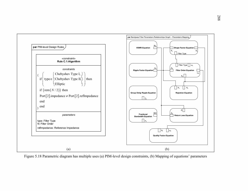
288
par PIM-level Design Rules
«constraint»Rule C.1:Algorithm
constraints
parameters
type: Filter TypeN: Filter Order
refImpedance: Reference Impedance
( )( )[ ] [ ]
Chebyshev Type I,
if type Chebyshev Type II, then
Elliptic
if rem / 2 then
Port 2 .impedance Port 2 .refImpedance
end
end
N
∈
≠
par Bandpass Filter Parameters Relationships Graph – Parameters Mapping
VSWR:Equation
Ripple Factor:Equation
Group Delay Ripple:Equation
Filter Order:Equation
Rejection:Equation
Fractional Bandwidth:Equation
Return Loss:Equation
Quality Factor:Equation
Shape Factor:Equation
Filter Type
As
ωs
ωp
Ap
As
As
Filter Type
Ap
ZS
ZL
θk ωp
BW
ζg
F0
RL
As Ap
(a) (b)
Figure 5.18 Parametric diagram has multiple uses (a) PIM-level design constraints, (b) Mapping of equations’ parameters
288
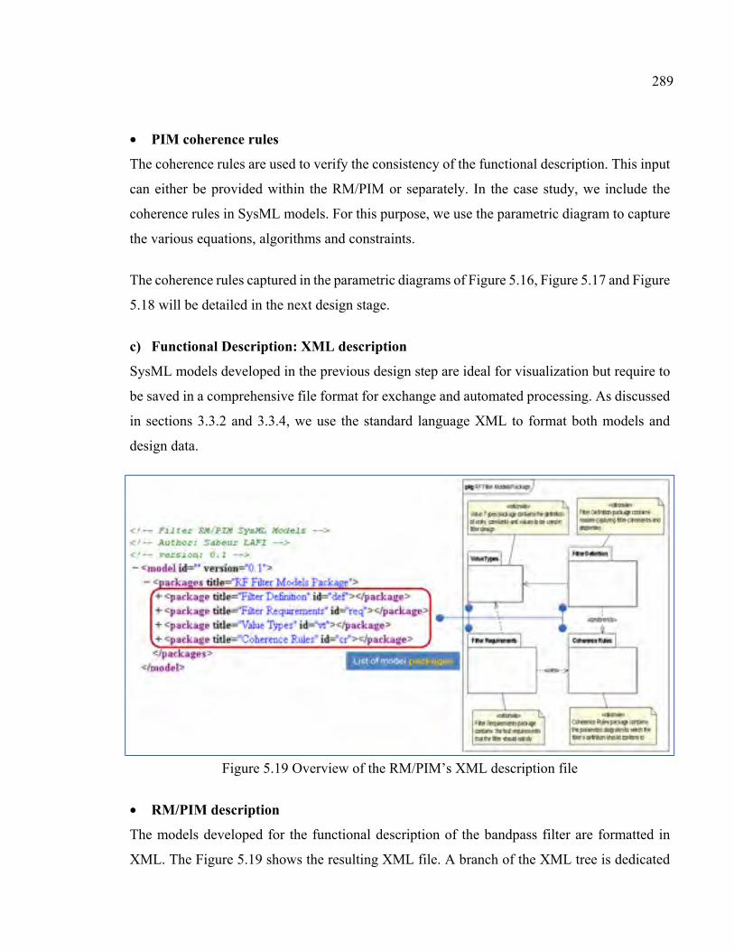
• PIM coherence rules
The coherence rules are used to verify the consistency of the functional description. This input
can either be provided within the RM/PIM or separately. In the case study, we include the
coherence rules in SysML models. For this purpose, we use the parametric diagram to capture
the various equations, algorithms and constraints.
The coherence rules captured in the parametric diagrams of Figure 5.16, Figure 5.17 and Figure
5.18 will be detailed in the next design stage.
c) Functional Description: XML description
SysML models developed in the previous design step are ideal for visualization but require to
be saved in a comprehensive file format for exchange and automated processing. As discussed
in sections 3.3.2 and 3.3.4, we use the standard language XML to format both models and
design data.
Figure 5.19 Overview of the RM/PIM’s XML description file
• RM/PIM description
The models developed for the functional description of the bandpass filter are formatted in
XML. The Figure 5.19 shows the resulting XML file. A branch of the XML tree is dedicated
289
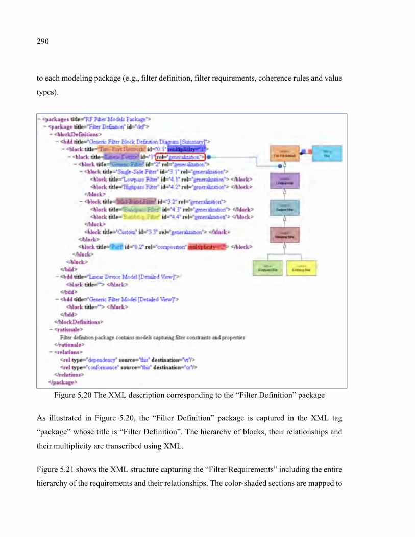
290
to each modeling package (e.g., filter definition, filter requirements, coherence rules and value
types).
Figure 5.20 The XML description corresponding to the “Filter Definition” package
As illustrated in Figure 5.20, the “Filter Definition” package is captured in the XML tag
“package” whose title is “Filter Definition”. The hierarchy of blocks, their relationships and
their multiplicity are transcribed using XML.
Figure 5.21 shows the XML structure capturing the “Filter Requirements” including the entire
hierarchy of the requirements and their relationships. The color-shaded sections are mapped to
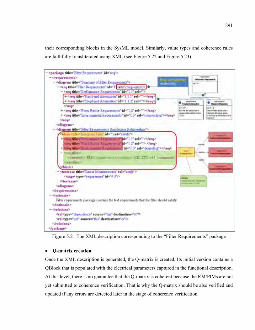
291
their corresponding blocks in the SysML model. Similarly, value types and coherence rules
are faithfully transliterated using XML (see Figure 5.22 and Figure 5.23).
Figure 5.21 The XML description corresponding to the “Filter Requirements” package
• Q-matrix creation
Once the XML description is generated, the Q-matrix is created. Its initial version contains a
QBlock that is populated with the electrical parameters captured in the functional description.
At this level, there is no guarantee that the Q-matrix is coherent because the RM/PIMs are not
yet submitted to coherence verification. That is why the Q-matrix should be also verified and
updated if any errors are detected later in the stage of coherence verification.
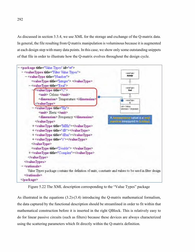
292
As discussed in section 3.3.4, we use XML for the storage and exchange of the Q-matrix data.
In general, the file resulting from Q matrix manipulation is voluminous because it is augmented
at each design step with many data points. In this case, we show only some outstanding snippets
of that file in order to illustrate how the Q-matrix evolves throughout the design cycle.
Figure 5.22 The XML description corresponding to the “Value Types” package
As illustrated in the equations (3.2)-(3.4) introducing the Q-matrix mathematical formalism,
the data captured by the functional description should be streamlined in order to fit within that
mathematical construction before it is inserted in the right QBlock. This is relatively easy to
do for linear passive circuits (such as filters) because these devices are always characterized
using the scattering parameters which fit directly within the Q-matrix definition.
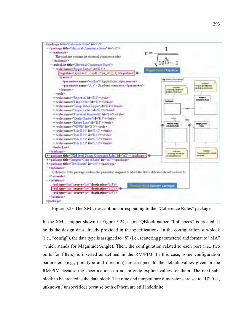
293
Figure 5.23 The XML description corresponding to the “Coherence Rules” package
In the XML snippet shown in Figure 5.24, a first QBlock named “bpf_specs” is created. It
holds the design data already provided in the specifications. In the configuration sub-block
(i.e., “config”), the data type is assigned to “S” (i.e., scattering parameters) and format to “MA”
(which stands for Magnitude/Angle). Then, the configuration related to each port (i.e., two
ports for filters) is inserted as defined in the RM/PIM. In this case, some configuration
parameters (e.g., port type and direction) are assigned to the default values given in the
RM/PIM because the specifications do not provide explicit values for them. The next sub-
block to be created is the data block. The time and temperature dimensions are set to “U” (i.e.,
unknown / unspecified) because both of them are still indefinite.
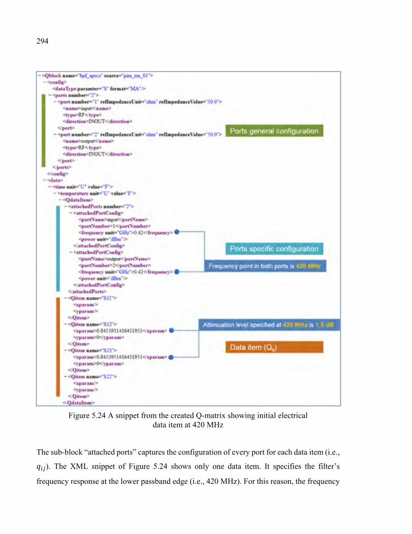
294
Figure 5.24 A snippet from the created Q-matrix showing initial electrical data item at 420 MHz
The sub-block “attached ports” captures the configuration of every port for each data item (i.e.,
). The XML snippet of Figure 5.24 shows only one data item. It specifies the filter’s
frequency response at the lower passband edge (i.e., 420 MHz). For this reason, the frequency
295
parameter of input and output ports is set to 0.42 GHz. No power level was specified in the
RM/PIM at this frequency for both ports, which explains why this parameter is void.
The attenuation level required at 420 MHz corresponds to the passband attenuation (i.e., equal
to 1.5 dB90). That is why the transmission coefficients and (named “S12” and “S21”
respectively) have a value equal to (0.841395, 0). The first refers to the magnitude while the
second is the angle. Since the value of the required attenuation is real, the imaginary part of
both coefficients is set zero. However, the reflection coefficients and (i.e., “S11” and
“S22”) are void because there is no data specified for them. In case of the return loss value
property in the port block is specified or assigned to a default value, it becomes mandatory to
calculate and at this step.
This initial Q-matrix reflects only the electrical data already captured by the functional
description (i.e., RIM/PIM). At this step, the Q-matrix is not complete and may be not coherent.
It is mandatory to review the Q-matrix at the coherence verification step in order to avoid any
errors. In the following design steps and stages, the Q-matrix continues to be populated with
additional data from various sources.
d) Analysis: Coherence verification
The functional description and the Q-matrix have not been submitted so far to any kind of
verification. Before starting the analysis step in order to find out an initial design solution
meeting the requirements, a coherence verification test should take place. This process uses a
set of coherence rules that are used to validate the consistency of the functional description. In
this case study, these rules are part of the RM/PIM and not provided as a separate input. We
used SysML parametric diagram to capture three types of coherence rules.
Let us first consider the following notations:
Filter order
Bandwidth
90 Mathematically speaking, an attenuation of 1.5 dB corresponds to a gain equal to -1.5 dB.
296
% Fractional Bandwidth
Central Frequency
Cutoff Frequency
Stopband Edge Frequency
Shape Factor
ripple
Group Delay
Passband Attenuation
Stopband Attenuation
Filter Selectivity or Rejection
Reference Impedance
Quality Factor
Return Loss
Noise Figure
• Electrical consistence rules
The electrical consistence rules check out the validity of the specified values regarding the
relationships linking them. For the bandpass filter, we developed the parameters relationships
graph (PRG) of Figure 5.25 in order to determine the links between its value properties. The
equations of Table 5.5 illustrate these links. The parametric diagram of Figure 5.18.b illustrates
how to map the same parameters in different equations for each rule. Such mapping avoids
ambiguity when complex mathematical formalisms are involved. It is worth noting that the
relationships given in Table 5. 5 are not exhaustive. We enumerate the remaining ones in Table
5.6. The SysML parametric diagram of Figure 5.16 captures all these rules.
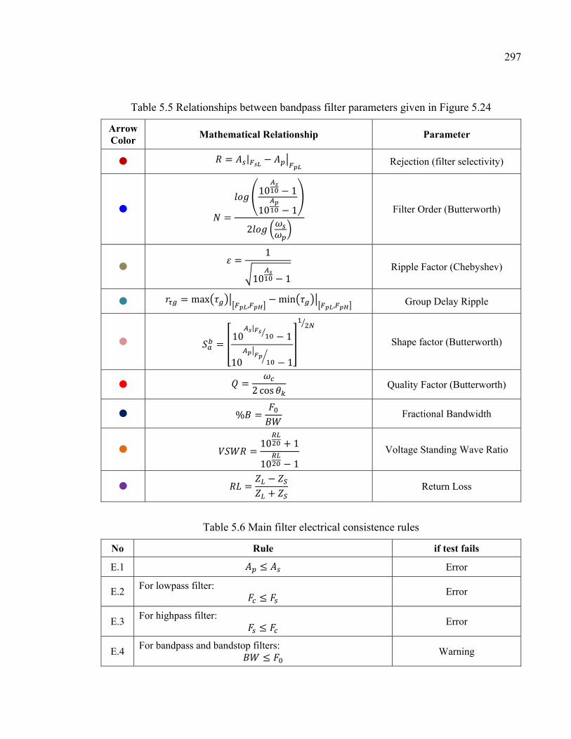
297
Table 5.5 Relationships between bandpass filter parameters given in Figure 5.24
Arrow Color
Mathematical Relationship Parameter
= | − Rejection (filter selectivity)
= 10 − 110 − 12 Filter Order (Butterworth)
= 110 − 1
Ripple Factor (Chebyshev)
= max , − min , Group Delay Ripple
= 10 | − 110 − 1 Shape factor (Butterworth)
= 2 cos Quality Factor (Butterworth)
% = Fractional Bandwidth
= 10 + 110 − 1 Voltage Standing Wave Ratio
= −+ Return Loss
Table 5.6 Main filter electrical consistence rules
No Rule if test fails
E.1 ≤ Error
E.2 For lowpass filter: ≤
Error
E.3 For highpass filter: ≤ Error
E.4 For bandpass and bandstop filters: ≤
Warning
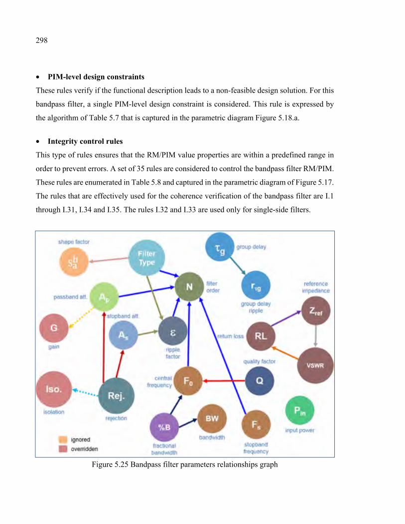
298
• PIM-level design constraints
These rules verify if the functional description leads to a non-feasible design solution. For this
bandpass filter, a single PIM-level design constraint is considered. This rule is expressed by
the algorithm of Table 5.7 that is captured in the parametric diagram Figure 5.18.a.
• Integrity control rules
This type of rules ensures that the RM/PIM value properties are within a predefined range in
order to prevent errors. A set of 35 rules are considered to control the bandpass filter RM/PIM.
These rules are enumerated in Table 5.8 and captured in the parametric diagram of Figure 5.17.
The rules that are effectively used for the coherence verification of the bandpass filter are I.1
through I.31, I.34 and I.35. The rules I.32 and I.33 are used only for single-side filters.
Figure 5.25 Bandpass filter parameters relationships graph
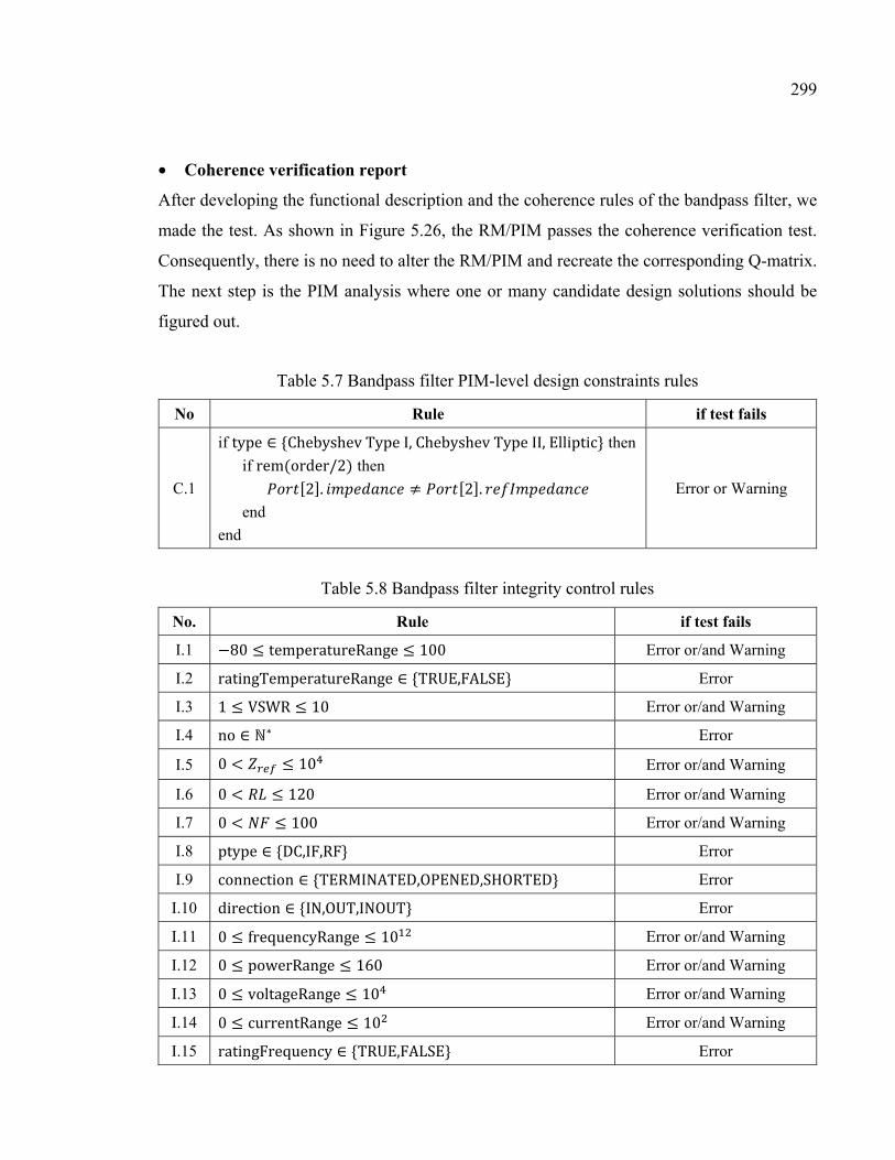
299
• Coherence verification report
After developing the functional description and the coherence rules of the bandpass filter, we
made the test. As shown in Figure 5.26, the RM/PIM passes the coherence verification test.
Consequently, there is no need to alter the RM/PIM and recreate the corresponding Q-matrix.
The next step is the PIM analysis where one or many candidate design solutions should be
figured out.
Table 5.7 Bandpass filter PIM-level design constraints rules
No Rule if test fails
C.1
if type ∈ ChebyshevTypeI,ChebyshevTypeII,Elliptic then
if rem(order/2) then [2]. ≠ [2].
end
end
Error or Warning
Table 5.8 Bandpass filter integrity control rules
No. Rule if test fails
I.1 −80 ≤ temperatureRange ≤ 100 Error or/and Warning
I.2 ratingTemperatureRange ∈ TRUE,FALSE Error
I.3 1 ≤ VSWR ≤ 10 Error or/and Warning
I.4 no ∈ ℕ∗ Error
I.5 0 < ≤ 10 Error or/and Warning
I.6 0 < ≤ 120 Error or/and Warning
I.7 0 < ≤ 100 Error or/and Warning
I.8 ptype ∈ DC,IF,RF Error
I.9 connection ∈ TERMINATED,OPENED,SHORTED Error
I.10 direction ∈ IN,OUT,INOUT Error
I.11 0 ≤ frequencyRange ≤ 10 Error or/and Warning
I.12 0 ≤ powerRange ≤ 160 Error or/and Warning
I.13 0 ≤ voltageRange ≤ 10 Error or/and Warning
I.14 0 ≤ currentRange ≤ 10 Error or/and Warning
I.15 ratingFrequency ∈ TRUE,FALSE Error
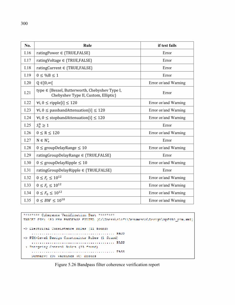
300
No. Rule if test fails
I.16 ratingPower ∈ TRUE,FALSE Error
I.17 ratingVoltage ∈ TRUE,FALSE Error
I.18 ratingCurrent ∈ TRUE,FALSE Error
I.19 0 ≤ %B ≤ 1 Error
I.20 Q ∈]0,∞[ Error or/and Warning
I.21 type ∈ Bessel,Butterworth,ChebyshevTypeI,ChebyshevTypeII,Custom,Elliptic Error
I.22 ∀i, 0 ≤ ripple[i] ≤ 120 Error or/and Warning
I.23 ∀i, 0 ≤ passbandAttenuation[i] ≤ 120 Error or/and Warning
I.24 ∀i, 0 ≤ stopbandAttenuation[i] ≤ 120 Error or/and Warning
I.25 ≥ 1 Error
I.26 0 ≤ R ≤ 120 Error or/and Warning
I.27 N ∈ ℕ∗ Error
I.28 0 ≤ groupDelayRange ≤ 10 Error or/and Warning
I.29 ratingGroupDelayRange ∈ TRUE,FALSE Error
I.30 0 ≤ groupDelayRipple ≤ 10 Error or/and Warning
I.31 ratingGroupDelayRipple ∈ TRUE,FALSE Error
I.32 0 ≤ ≤ 10 Error or/and Warning
I.33 0 ≤ ≤ 10 Error or/and Warning
I.34 0 ≤ ≤ 10 Error or/and Warning
I.35 0 ≤ ≤ 10 Error or/and Warning
Figure 5.26 Bandpass filter coherence verification report
301
e) Analysis: PIM-level granularity refinement and simulation
At this step, the functional description passed the coherence verification test. We need to find
out design solutions that meet the requirements of that functional description.
• Design space exploration
To figure out a candidate design solution that fits with the filter’s functional description, we
associate a black-box model to it (see section 4.3.3). This black-box model is mathematically
defined by the equation (A III-1, p. 451) in APPENDIX III. Hence, the functional description
provides an abstract representation of the filter functionality while the black-box model
provides a theoretical realization of that functionality. From this viewpoint, the relationship
between the functional description and the associated black-box model is similar (but not
identical) to the relationship between a class and an object (i.e., an instantiation of that class)
in object-oriented programming91.
We consider four traditional approximations for the filter transfer function on which the black-
box model is based. These approximations are:
− Butterworth,
− Chebyshev Type I,
− Elliptic (aka Cauer), and
− Bessel.
The equations (A III-5, p. 452) and (A III-8, p. 452) in APPENDIX III give the transfer
functions related to Butterworth and Chebyshev Type I approximations. The reader can refer
to (Wanhammar, 2009) for a thorough dissertation about the mathematical background of all
these approximations.
Based on the PIM, the analysis of the black-model (i.e., four filter prototypes) gives the
frequency and group delay responses shown in Figure 5.27. The Table 5.9 shows a detailed
comparison between the performances of these prototypes. This comparison is based on the
91 See section 4.2.4.b.
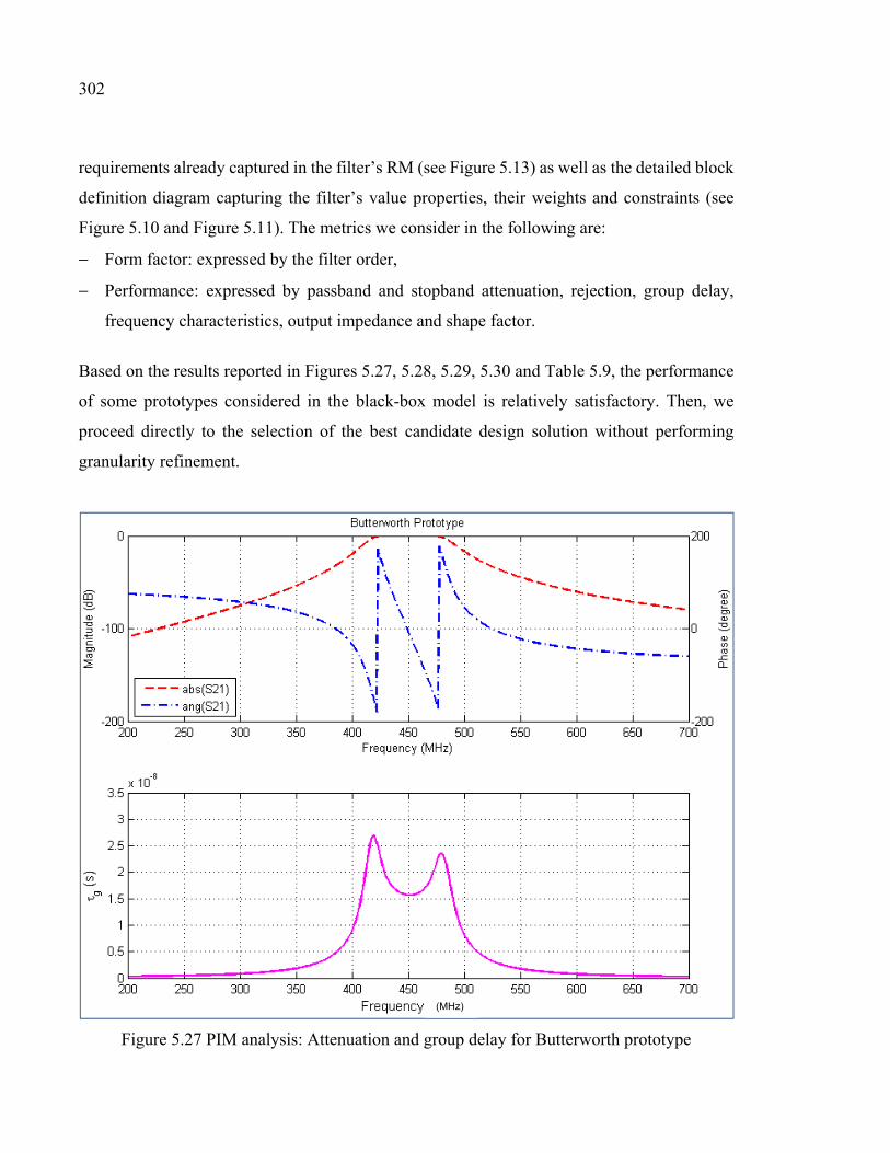
302
requirements already captured in the filter’s RM (see Figure 5.13) as well as the detailed block
definition diagram capturing the filter’s value properties, their weights and constraints (see
Figure 5.10 and Figure 5.11). The metrics we consider in the following are:
− Form factor: expressed by the filter order,
− Performance: expressed by passband and stopband attenuation, rejection, group delay,
frequency characteristics, output impedance and shape factor.
Based on the results reported in Figures 5.27, 5.28, 5.29, 5.30 and Table 5.9, the performance
of some prototypes considered in the black-box model is relatively satisfactory. Then, we
proceed directly to the selection of the best candidate design solution without performing
granularity refinement.
Figure 5.27 PIM analysis: Attenuation and group delay for Butterworth prototype
(MHz)
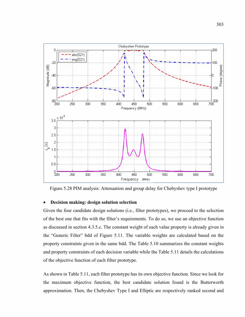
303
Figure 5.28 PIM analysis: Attenuation and group delay for Chebyshev type I prototype
• Decision making: design solution selection
Given the four candidate design solutions (i.e., filter prototypes), we proceed to the selection
of the best one that fits with the filter’s requirements. To do so, we use an objective function
as discussed in section 4.3.5.c. The constant weight of each value property is already given in
the “Generic Filter” bdd of Figure 5.11. The variable weights are calculated based on the
property constraints given in the same bdd. The Table 5.10 summarizes the constant weights
and property constraints of each decision variable while the Table 5.11 details the calculations
of the objective function of each filter prototype.
As shown in Table 5.11, each filter prototype has its own objective function. Since we look for
the maximum objective function, the best candidate solution found is the Butterworth
approximation. Then, the Chebyshev Type I and Elliptic are respectively ranked second and
(MHz)
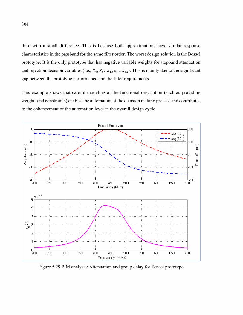
304
third with a small difference. This is because both approximations have similar response
characteristics in the passband for the same filter order. The worst design solution is the Bessel
prototype. It is the only prototype that has negative variable weights for stopband attenuation
and rejection decision variables (i.e., , , and ). This is mainly due to the significant
gap between the prototype performance and the filter requirements.
This example shows that careful modeling of the functional description (such as providing
weights and constraints) enables the automation of the decision making process and contributes
to the enhancement of the automation level in the overall design cycle.
Figure 5.29 PIM analysis: Attenuation and group delay for Bessel prototype
(MHz)
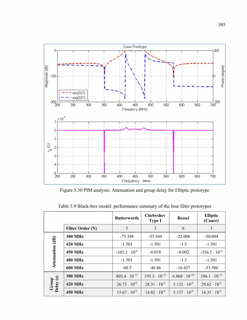
305
Figure 5.30 PIM analysis: Attenuation and group delay for Elliptic prototype
Table 5.9 Black-box model: performance summary of the four filter prototypes
Butterworth Chebyshev
Type I Bessel
Elliptic (Cauer)
Filter Order (N) 5 3 6 3
Att
enu
atio
n (
dB
) 300 MHz -75.394 -55.569 -22.006 -50.004
420 MHz -1.501 -1.501 -1.5 -1.501
450 MHz -385.2 ⋅ 10-6 -0.018 -0.002 -356.5 ⋅ 10-6
480 MHz -1.501 -1.501 -1.5 -1.501
600 MHz -60.5 -46.46 -16.437 -53.586
Gro
up
D
elay
(s)
300 MHz 805.4 ⋅ 10-12 195.3 ⋅ 10-12 6.868 ⋅ 10-10 194.1 ⋅ 10-12
420 MHz 26.73 ⋅ 10-9 28.31 ⋅ 10-9 5.132 ⋅ 10-9 29.62 ⋅ 10-9
450 MHz 15.67 ⋅ 10-9 14.82 ⋅ 10-9 5.137 ⋅ 10-9 14.35 ⋅ 10-9
(MHz)
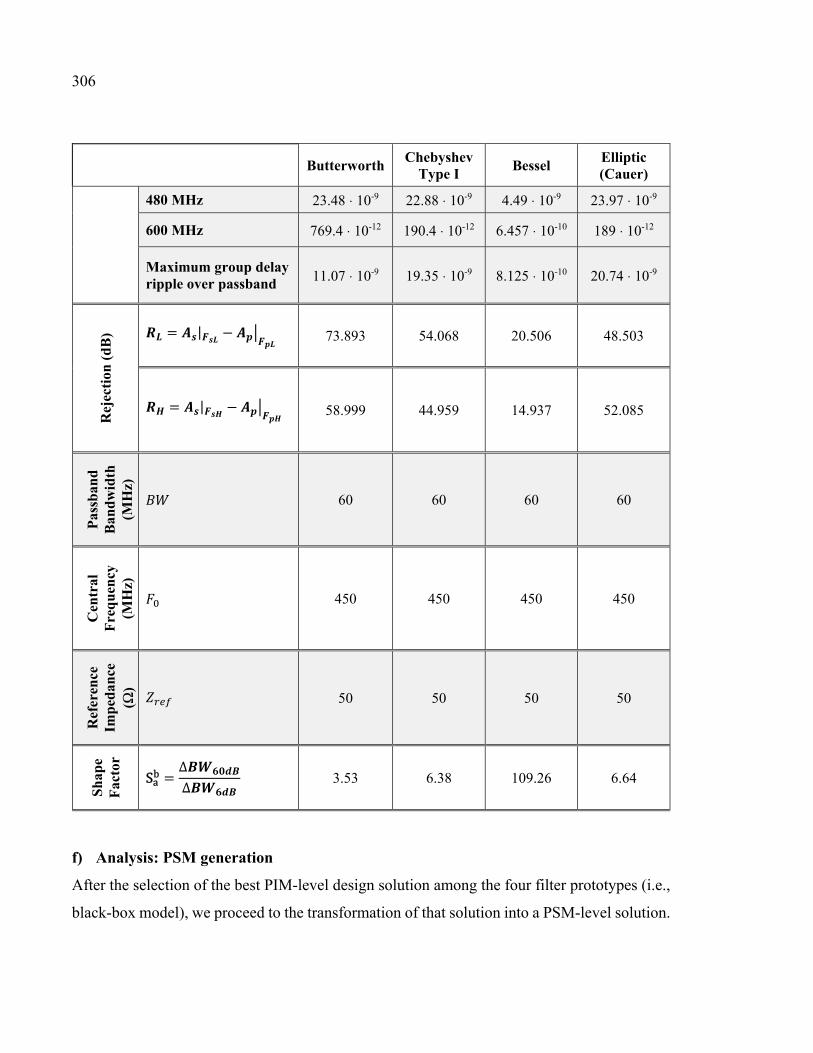
306
Butterworth Chebyshev
Type I Bessel
Elliptic (Cauer)
480 MHz 23.48 ⋅ 10-9 22.88 ⋅ 10-9 4.49 ⋅ 10-9 23.97 ⋅ 10-9
600 MHz 769.4 ⋅ 10-12 190.4 ⋅ 10-12 6.457 ⋅ 10-10 189 ⋅ 10-12
Maximum group delay ripple over passband 11.07 ⋅ 10-9 19.35 ⋅ 10-9 8.125 ⋅ 10-10 20.74 ⋅ 10-9
Rej
ecti
on (
dB
) = | − 73.893 54.068 20.506 48.503
= | − 58.999 44.959 14.937 52.085
Pas
sban
d
Ban
dw
idth
(M
Hz)
60 60 60 60
Cen
tral
F
req
uen
cy
(MH
z)
450 450 450 450
Ref
eren
ce
Imp
edan
ce
(Ω)
50 50 50 50
Sh
ape
Fac
tor Sab = ∆∆ 3.53 6.38 109.26 6.64
f) Analysis: PSM generation
After the selection of the best PIM-level design solution among the four filter prototypes (i.e.,
black-box model), we proceed to the transformation of that solution into a PSM-level solution.
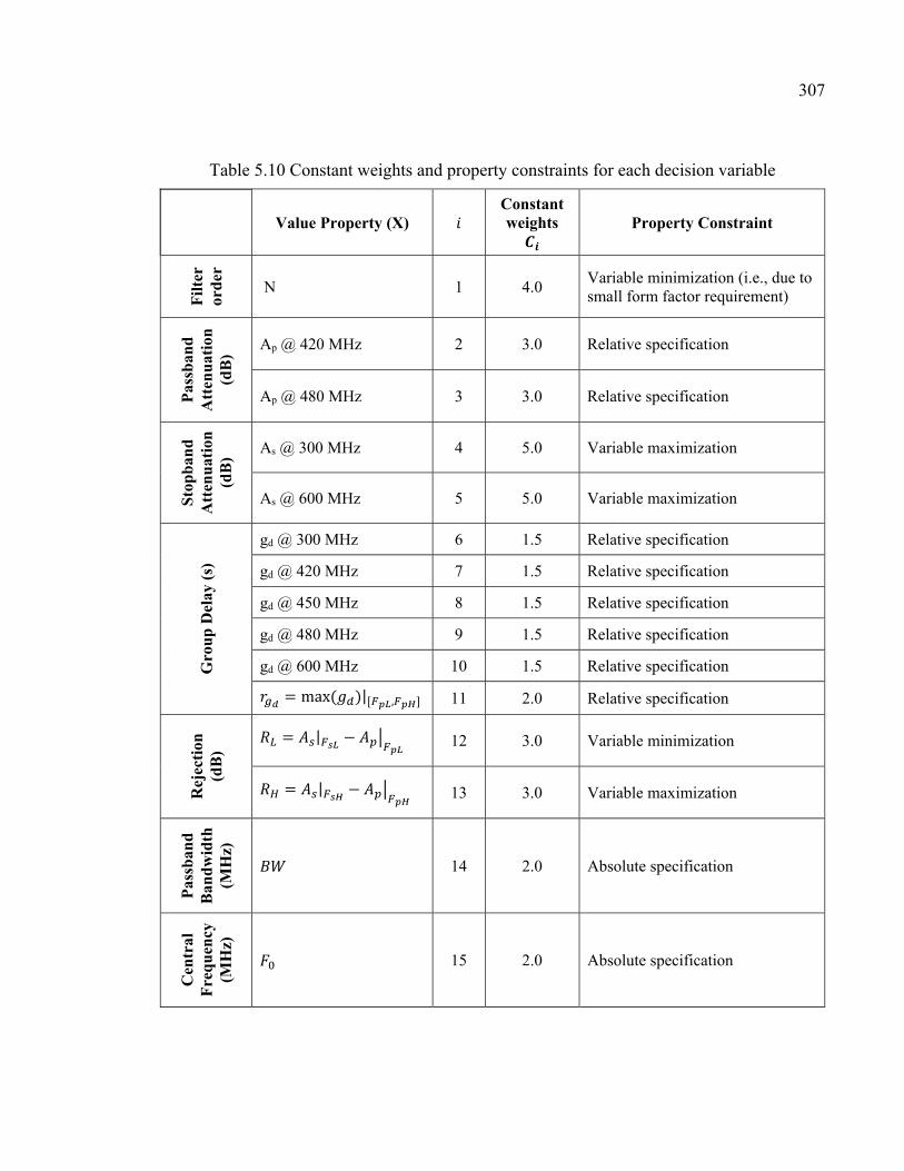
307
Table 5.10 Constant weights and property constraints for each decision variable
Value Property (X) Constant weights
Property Constraint
Fil
ter
ord
er
N 1 4.0 Variable minimization (i.e., due to small form factor requirement)
Pas
sban
d
Att
enu
atio
n
(dB
)
Ap @ 420 MHz 2 3.0 Relative specification
Ap @ 480 MHz 3 3.0 Relative specification
Sto
pb
and
A
tten
uat
ion
(d
B)
As @ 300 MHz 4 5.0 Variable maximization
As @ 600 MHz 5 5.0 Variable maximization
Gro
up
Del
ay (
s)
gd @ 300 MHz 6 1.5 Relative specification
gd @ 420 MHz 7 1.5 Relative specification
gd @ 450 MHz 8 1.5 Relative specification
gd @ 480 MHz 9 1.5 Relative specification
gd @ 600 MHz 10 1.5 Relative specification = max( )|[ , ] 11 2.0 Relative specification
Rej
ecti
on
(dB
)
= | − 12 3.0 Variable minimization
= | − 13 3.0 Variable maximization
Pas
sban
d
Ban
dw
idth
(M
Hz)
14 2.0 Absolute specification
Cen
tral
F
req
uen
cy
(MH
z)
15 2.0 Absolute specification
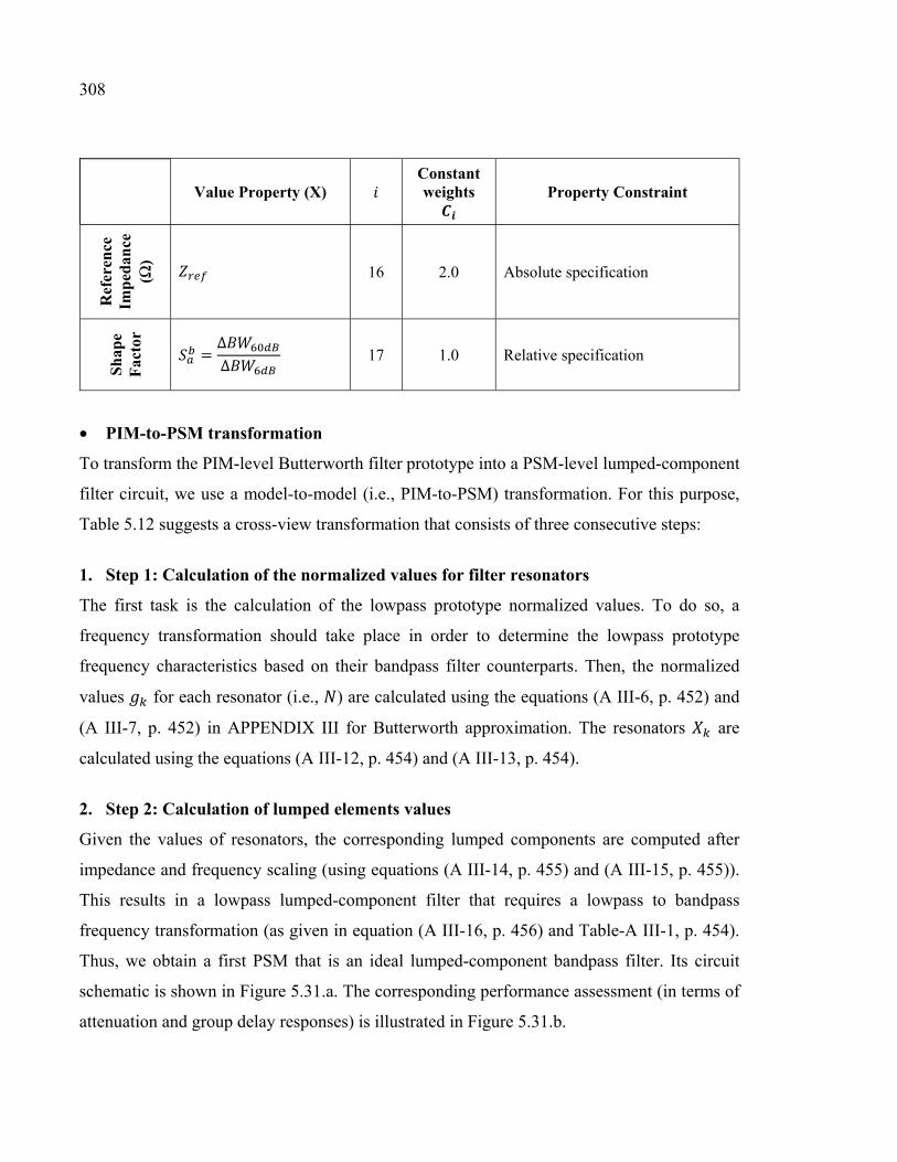
308
Value Property (X) Constant weights
Property Constraint
Ref
eren
ce
Imp
edan
ce
(Ω)
16 2.0 Absolute specification
Sh
ape
Fac
tor = ∆∆ 17 1.0 Relative specification
• PIM-to-PSM transformation
To transform the PIM-level Butterworth filter prototype into a PSM-level lumped-component
filter circuit, we use a model-to-model (i.e., PIM-to-PSM) transformation. For this purpose,
Table 5.12 suggests a cross-view transformation that consists of three consecutive steps:
1. Step 1: Calculation of the normalized values for filter resonators
The first task is the calculation of the lowpass prototype normalized values. To do so, a
frequency transformation should take place in order to determine the lowpass prototype
frequency characteristics based on their bandpass filter counterparts. Then, the normalized
values for each resonator (i.e., ) are calculated using the equations (A III-6, p. 452) and
(A III-7, p. 452) in APPENDIX III for Butterworth approximation. The resonators are
calculated using the equations (A III-12, p. 454) and (A III-13, p. 454).
2. Step 2: Calculation of lumped elements values
Given the values of resonators, the corresponding lumped components are computed after
impedance and frequency scaling (using equations (A III-14, p. 455) and (A III-15, p. 455)).
This results in a lowpass lumped-component filter that requires a lowpass to bandpass
frequency transformation (as given in equation (A III-16, p. 456) and Table-A III-1, p. 454).
Thus, we obtain a first PSM that is an ideal lumped-component bandpass filter. Its circuit
schematic is shown in Figure 5.31.a. The corresponding performance assessment (in terms of
attenuation and group delay responses) is illustrated in Figure 5.31.b.

309
3. Step 3: Synthesis of transmission lines and circuit topology
The PSM generated in step 2 satisfies the requirements of the functional description. However,
it is still not practically realizable because there are no physical connections between the
lumped components. In step 3 of the PIM-to-PSM transformation, we alter the topology of
each resonator (as illustrated in Figure 5.32.a and Figure 5.32.b) in order to physically connect
each lumped component to the others. This takes place by adding several sections of planar
transmission lines. The final PSM circuit is shown in Figure 5.33.
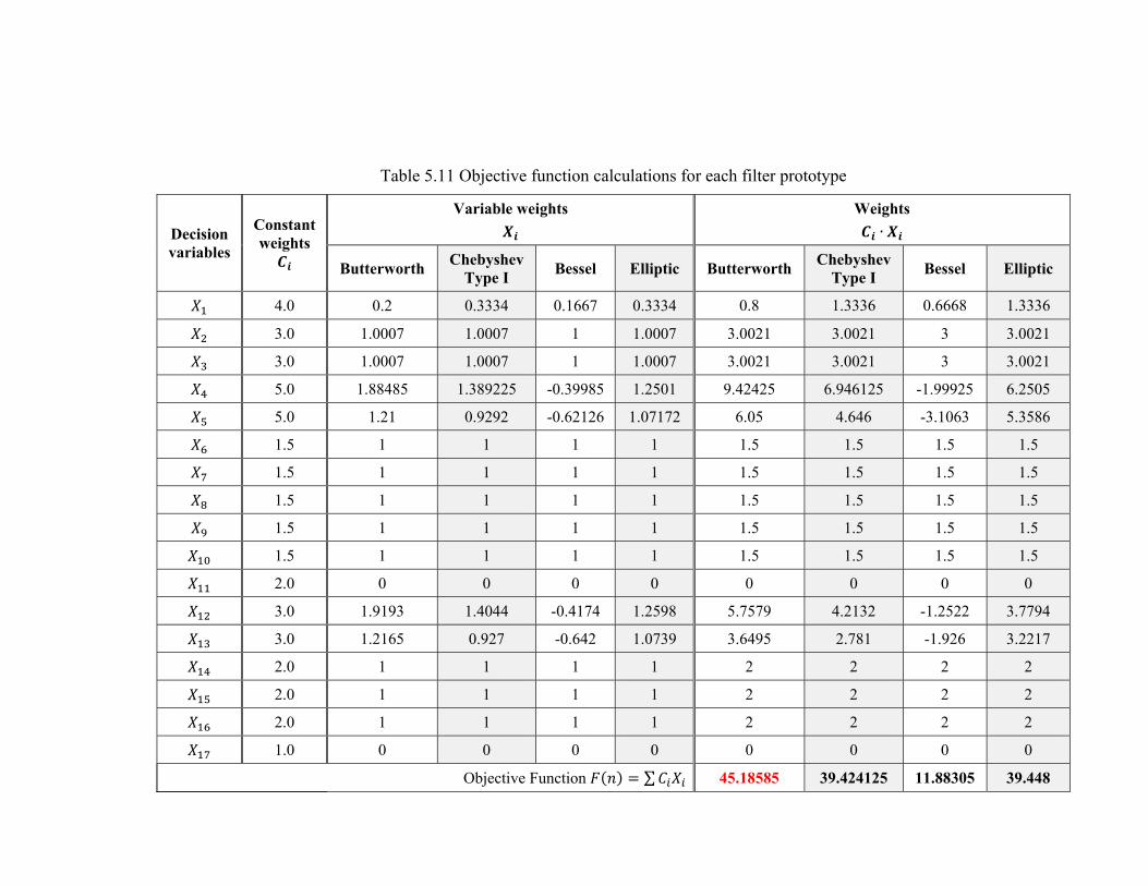
Table 5.11 Objective function calculations for each filter prototype
Decision variables
Constant weights
Variable weights
Weights ∙
Butterworth Chebyshev
Type I Bessel Elliptic Butterworth
Chebyshev Type I
Bessel Elliptic
4.0 0.2 0.3334 0.1667 0.3334 0.8 1.3336 0.6668 1.3336
3.0 1.0007 1.0007 1 1.0007 3.0021 3.0021 3 3.0021
3.0 1.0007 1.0007 1 1.0007 3.0021 3.0021 3 3.0021
5.0 1.88485 1.389225 -0.39985 1.2501 9.42425 6.946125 -1.99925 6.2505
5.0 1.21 0.9292 -0.62126 1.07172 6.05 4.646 -3.1063 5.3586
1.5 1 1 1 1 1.5 1.5 1.5 1.5
1.5 1 1 1 1 1.5 1.5 1.5 1.5
1.5 1 1 1 1 1.5 1.5 1.5 1.5
1.5 1 1 1 1 1.5 1.5 1.5 1.5
1.5 1 1 1 1 1.5 1.5 1.5 1.5
2.0 0 0 0 0 0 0 0 0
3.0 1.9193 1.4044 -0.4174 1.2598 5.7579 4.2132 -1.2522 3.7794
3.0 1.2165 0.927 -0.642 1.0739 3.6495 2.781 -1.926 3.2217
2.0 1 1 1 1 2 2 2 2
2.0 1 1 1 1 2 2 2 2
2.0 1 1 1 1 2 2 2 2
1.0 0 0 0 0 0 0 0 0
Objective Function ( ) = ∑ 45.18585 39.424125 11.88305 39.448
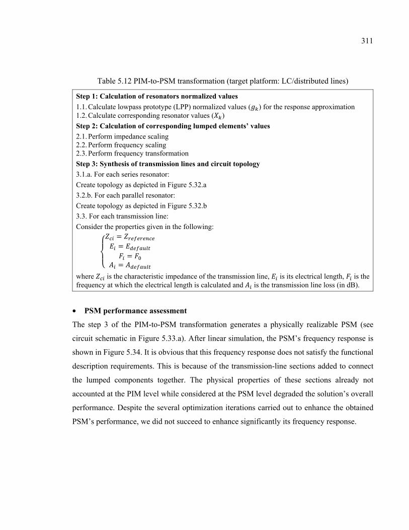
311
Table 5.12 PIM-to-PSM transformation (target platform: LC/distributed lines)
Step 1: Calculation of resonators normalized values
1.1. Calculate lowpass prototype (LPP) normalized values ( ) for the response approximation 1.2. Calculate corresponding resonator values ( )
Step 2: Calculation of corresponding lumped elements’ values
2.1. Perform impedance scaling 2.2. Perform frequency scaling 2.3. Perform frequency transformation
Step 3: Synthesis of transmission lines and circuit topology
3.1.a. For each series resonator:
Create topology as depicted in Figure 5.32.a
3.2.b. For each parallel resonator:
Create topology as depicted in Figure 5.32.b
3.3. For each transmission line:
Consider the properties given in the following: == ==
where is the characteristic impedance of the transmission line, is its electrical length, is the frequency at which the electrical length is calculated and is the transmission line loss (in dB).
• PSM performance assessment
The step 3 of the PIM-to-PSM transformation generates a physically realizable PSM (see
circuit schematic in Figure 5.33.a). After linear simulation, the PSM’s frequency response is
shown in Figure 5.34. It is obvious that this frequency response does not satisfy the functional
description requirements. This is because of the transmission-line sections added to connect
the lumped components together. The physical properties of these sections already not
accounted at the PIM level while considered at the PSM level degraded the solution’s overall
performance. Despite the several optimization iterations carried out to enhance the obtained
PSM’s performance, we did not succeed to enhance significantly its frequency response.
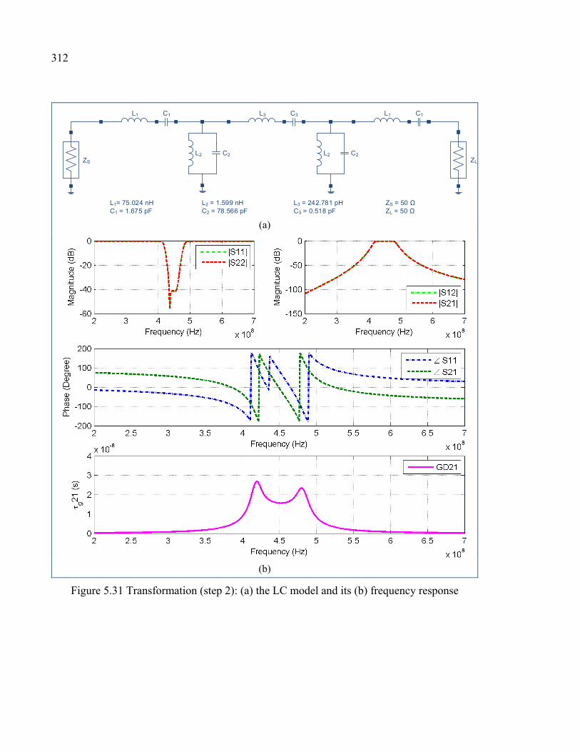
312
ZS
C1L1
C2
C3L3 C1L1
C2ZL
L2L2
L1= 75.024 nHC1 = 1.675 pF
L2 = 1.599 nHC2 = 78.566 pF
ZS = 50 Ω ZL = 50 Ω
L3 = 242.781 pHC3 = 0.518 pF
(a)
(b)
Figure 5.31 Transformation (step 2): (a) the LC model and its (b) frequency response
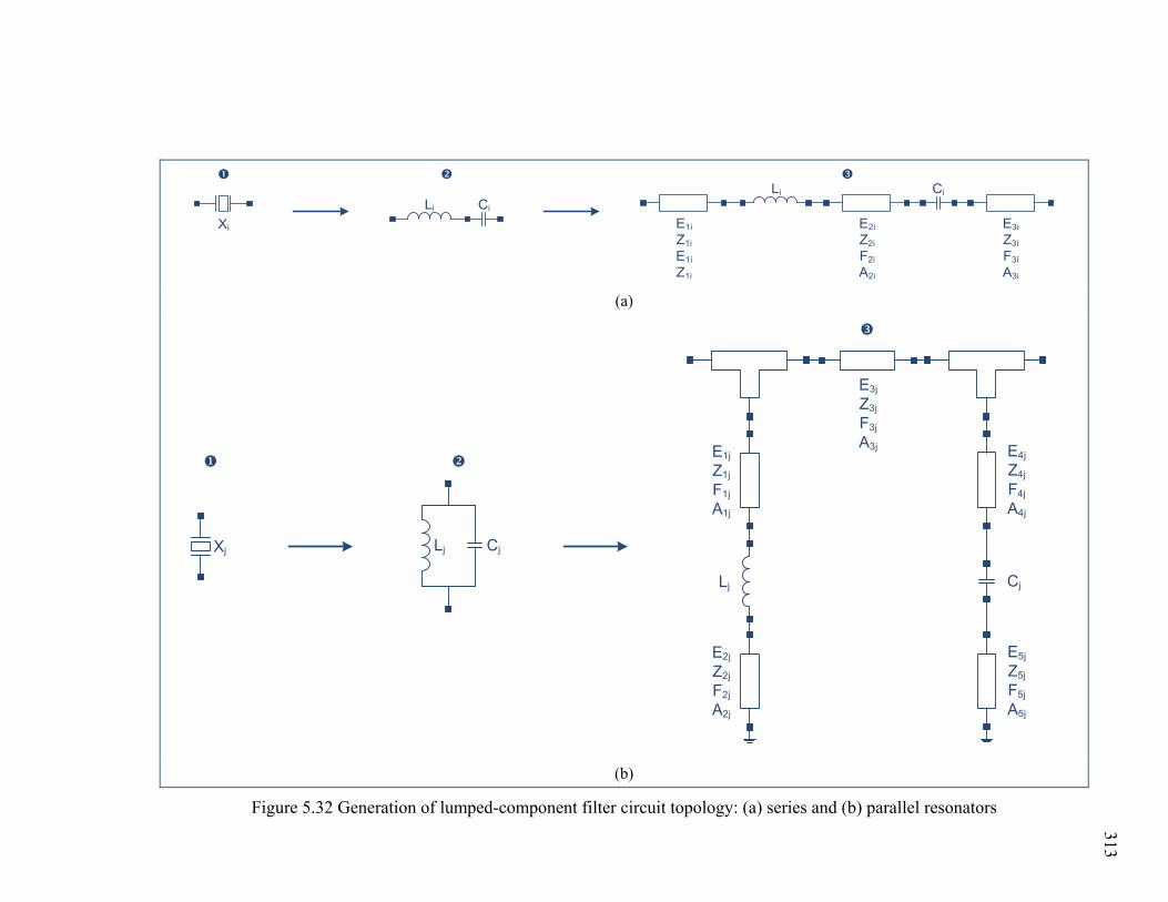
CiLi
CiLi
E1i
Z1i
E1i
Z1i
E2i
Z2i
F2i
A2i
E3i
Z3i
F3i
A3i
Xi
(a)
Xj CjLj
CjLj
E1j
Z1j
F1j
A1j
E3j
Z3j
F3j
A3j E4j
Z4j
F4j
A4j
E2j
Z2j
F2j
A2j
E5j
Z5j
F5j
A5j
(b)
Figure 5.32 Generation of lumped-component filter circuit topology: (a) series and (b) parallel resonators
313
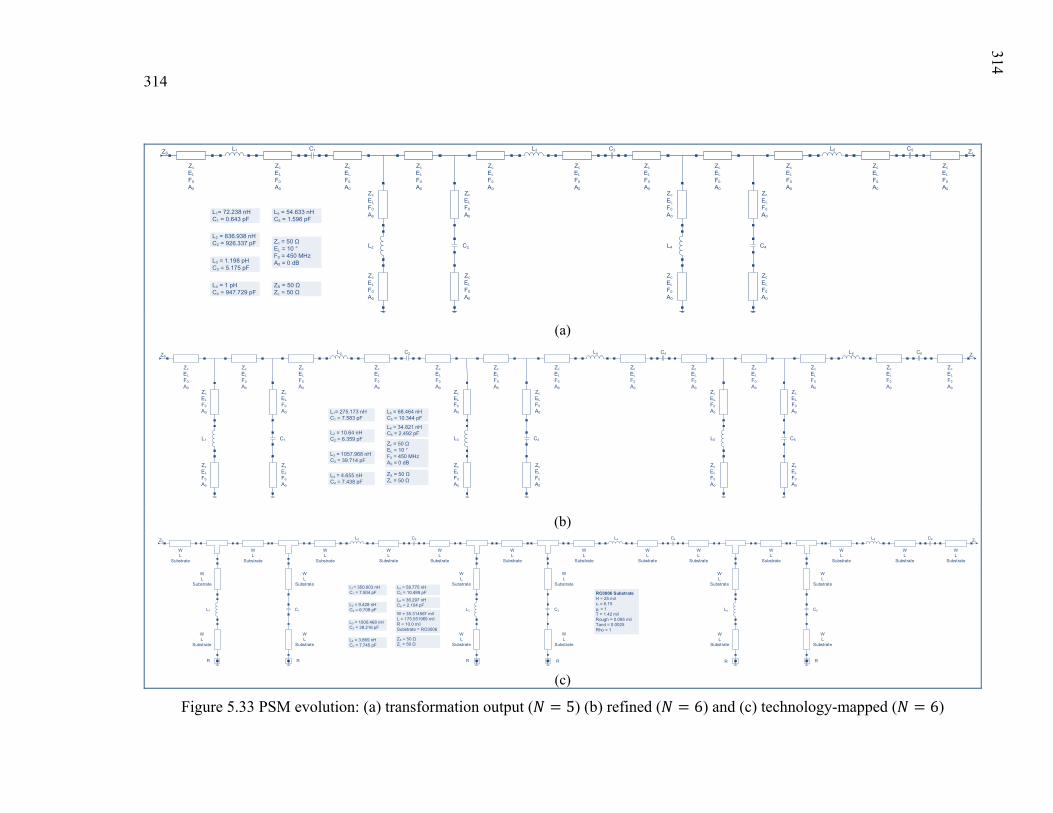
314
C1L1 C3L3 C5L5
C2L2 L4 C4
Zc
EL
F0
A0
Zc
EL
F0
A0
Zc
EL
F0
A0
Zc
EL
F0
A0
Zc
EL
F0
A0
Zc
EL
F0
A0
Zc
EL
F0
A0
Zc
EL
F0
A0
Zc
EL
F0
A0
Zc
EL
F0
A0
Zc
EL
F0
A0
Zc
EL
F0
A0
Zc
EL
F0
A0
Zc
EL
F0
A0
Zc
EL
F0
A0
Zc
EL
F0
A0
Zc
EL
F0
A0
Zc
EL
F0
A0
Zc
EL
F0
A0
L1= 72.238 nHC1 = 0.643 pF
L2 = 836.938 nHC2 = 926.337 pF Zc = 50 Ω
EL = 10 °F0 = 450 MHzA0 = 0 dBL3 = 1.198 pH
C3 = 5.175 pF
L4 = 1 pHC4 = 947.729 pF
ZS = 50 Ω ZL = 50 Ω
L5 = 54.633 nHC5 = 1.596 pF
ZS ZL
(a) C2L2 C4L4 C6L6
C3L3 L5 C5
Zc
EL
F0
A0
Zc
EL
F0
A0
Zc
EL
F0
A0
Zc
EL
F0
A0
Zc
EL
F0
A0
Zc
EL
F0
A0
Zc
EL
F0
A0
Zc
EL
F0
A0
Zc
EL
F0
A0
Zc
EL
F0
A0
Zc
EL
F0
A0
Zc
EL
F0
A0
Zc
EL
F0
A0
Zc
EL
F0
A0
Zc
EL
F0
A0
Zc
EL
F0
A0
Zc
EL
F0
A0
Zc
EL
F0
A0
Zc
EL
F0
A0
L1= 275.173 nHC1 = 7.583 pF
L2 = 10.64 nHC2 = 6.359 pF
Zc = 50 Ω EL = 10 °F0 = 450 MHzA0 = 0 dB
L3 = 1057.968 nHC3 = 39.714 pF
L4 = 4.655 nHC4 = 7.438 pF
ZS = 50 Ω ZL = 50 Ω
L5 = 68.464 nHC5 = 10.344 pF
L6 = 34.821 nHC6 = 2.492 pF
C1L1
Zc
EL
F0
A0
Zc
EL
F0
A0
Zc
EL
F0
A0
Zc
EL
F0
A0
Zc
EL
F0
A0
Zc
EL
F0
A0
ZS ZL
(b) C2L2 C4L4 C6L6
C3L3 L5 C5
WL
Substrate
WL
Substrate
WL
Substrate
WL
Substrate
WL
Substrate
WL
Substrate
WL
Substrate
WL
Substrate
WL
Substrate
WL
Substrate
WL
Substrate
WL
Substrate
WL
Substrate
WL
Substrate
WL
Substrate
WL
Substrate
WL
Substrate
WL
Substrate
WL
Substrate
L1= 350.003 nHC1 = 7.504 pF
L2 = 9.428 nHC2 = 6.709 pF
W = 35.314567 mil L = 175.551969 milR = 10.0 milSubstrate = RO3006
L3 = 1000.468 nHC3 = 39.216 pF
L4 = 3.869 nHC4 = 7.745 pF
ZS = 50 Ω ZL = 50 Ω
L5 = 58.775 nHC5 = 10.489 pF
L6 = 36.297 nHC6 = 2.104 pF
C1L1
WL
Substrate
WL
Substrate
WL
Substrate
WL
Substrate
WL
Substrate
WL
Substrate
ZS ZL
R R R R R R
RO3006 SubstrateH = 25 milεr = 6.15 μr = 1 T = 1.42 milRough = 0.095 milTand = 0.0025Rho = 1
(c)
Figure 5.33 PSM evolution: (a) transformation output ( = 5) (b) refined ( = 6) and (c) technology-mapped ( = 6)
314
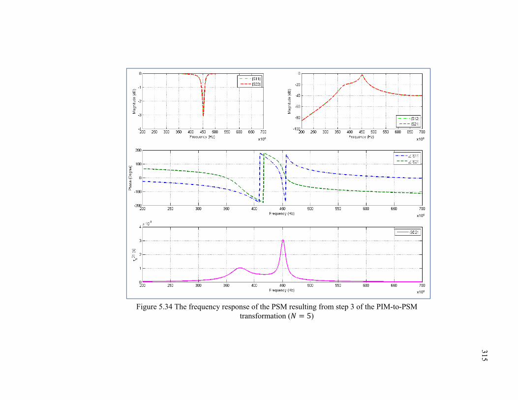
315
Figure 5.34 The frequency response of the PSM resulting from step 3 of the PIM-to-PSM transformation ( = 5)
315
x106
x106
x106 x106
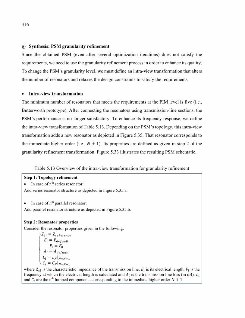
316
g) Synthesis: PSM granularity refinement
Since the obtained PSM (even after several optimization iterations) does not satisfy the
requirements, we need to use the granularity refinement process in order to enhance its quality.
To change the PSM’s granularity level, we must define an intra-view transformation that alters
the number of resonators and relaxes the design constraints to satisfy the requirements.
• Intra-view transformation
The minimum number of resonators that meets the requirements at the PIM level is five (i.e.,
Butterworth prototype). After connecting the resonators using transmission-line sections, the
PSM’s performance is no longer satisfactory. To enhance its frequency response, we define
the intra-view transformation of Table 5.13. Depending on the PSM’s topology, this intra-view
transformation adds a new resonator as depicted in Figure 5.35. That resonator corresponds to
the immediate higher order (i.e., + 1). Its properties are defined as given in step 2 of the
granularity refinement transformation. Figure 5.33 illustrates the resulting PSM schematic.
Table 5.13 Overview of the intra-view transformation for granularity refinement
Step 1: Topology refinement
• In case of nth series resonator:
Add series resonator structure as depicted in Figure 5.35.a.
• In case of nth parallel resonator:
Add parallel resonator structure as depicted in Figure 5.35.b.
Step 2: Resonator properties
Consider the resonator properties given in the following: == === |= |
where is the characteristic impedance of the transmission line, is its electrical length, is the frequency at which the electrical length is calculated and is the transmission line loss (in dB). and are the nth lumped components corresponding to the immediate higher order + 1.
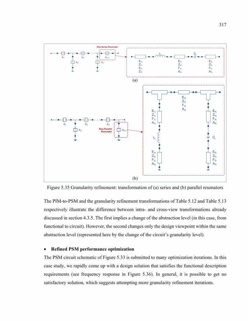
317
CiLi
E1i
Z1i
E1i
Z1i
E2i
Z2i
F2i
A2i
E3i
Z3i
F3i
A3i
...
X1 X3 Xn+1
X2 Xn
New Series Resonator
(a)
CjLj
E1j
Z1j
F1j
A1j
E3j
Z3j
F3j
A3j E4j
Z4j
F4j
A4j
E2j
Z2j
F2j
A2j
E5j
Z5j
F5j
A5j
...
X1 X3 Xn
X2 Xn+1New Parallel
Resonator
(b)
Figure 5.35 Granularity refinement: transformation of (a) series and (b) parallel resonators
The PIM-to-PSM and the granularity refinement transformations of Table 5.12 and Table 5.13
respectively illustrate the difference between intra- and cross-view transformations already
discussed in section 4.3.5. The first implies a change of the abstraction level (in this case, from
functional to circuit). However, the second changes only the design viewpoint within the same
abstraction level (represented here by the change of the circuit’s granularity level).
• Refined PSM performance optimization
The PSM circuit schematic of Figure 5.33 is submitted to many optimization iterations. In this
case study, we rapidly come up with a design solution that satisfies the functional description
requirements (see frequency response in Figure 5.36). In general, it is possible to get no
satisfactory solution, which suggests attempting more granularity refinement iterations.
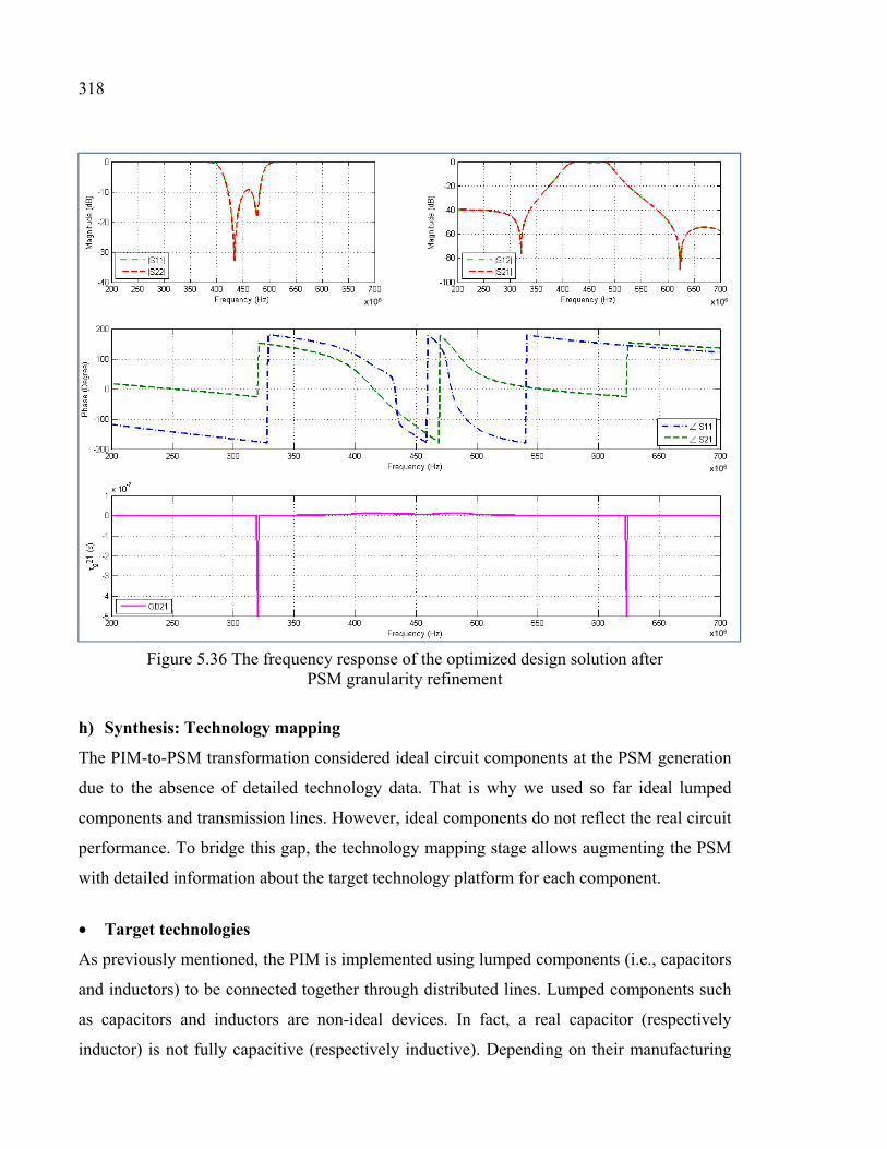
318
Figure 5.36 The frequency response of the optimized design solution after PSM granularity refinement
h) Synthesis: Technology mapping
The PIM-to-PSM transformation considered ideal circuit components at the PSM generation
due to the absence of detailed technology data. That is why we used so far ideal lumped
components and transmission lines. However, ideal components do not reflect the real circuit
performance. To bridge this gap, the technology mapping stage allows augmenting the PSM
with detailed information about the target technology platform for each component.
• Target technologies
As previously mentioned, the PIM is implemented using lumped components (i.e., capacitors
and inductors) to be connected together through distributed lines. Lumped components such
as capacitors and inductors are non-ideal devices. In fact, a real capacitor (respectively
inductor) is not fully capacitive (respectively inductive). Depending on their manufacturing
x106 x106
x106
x106
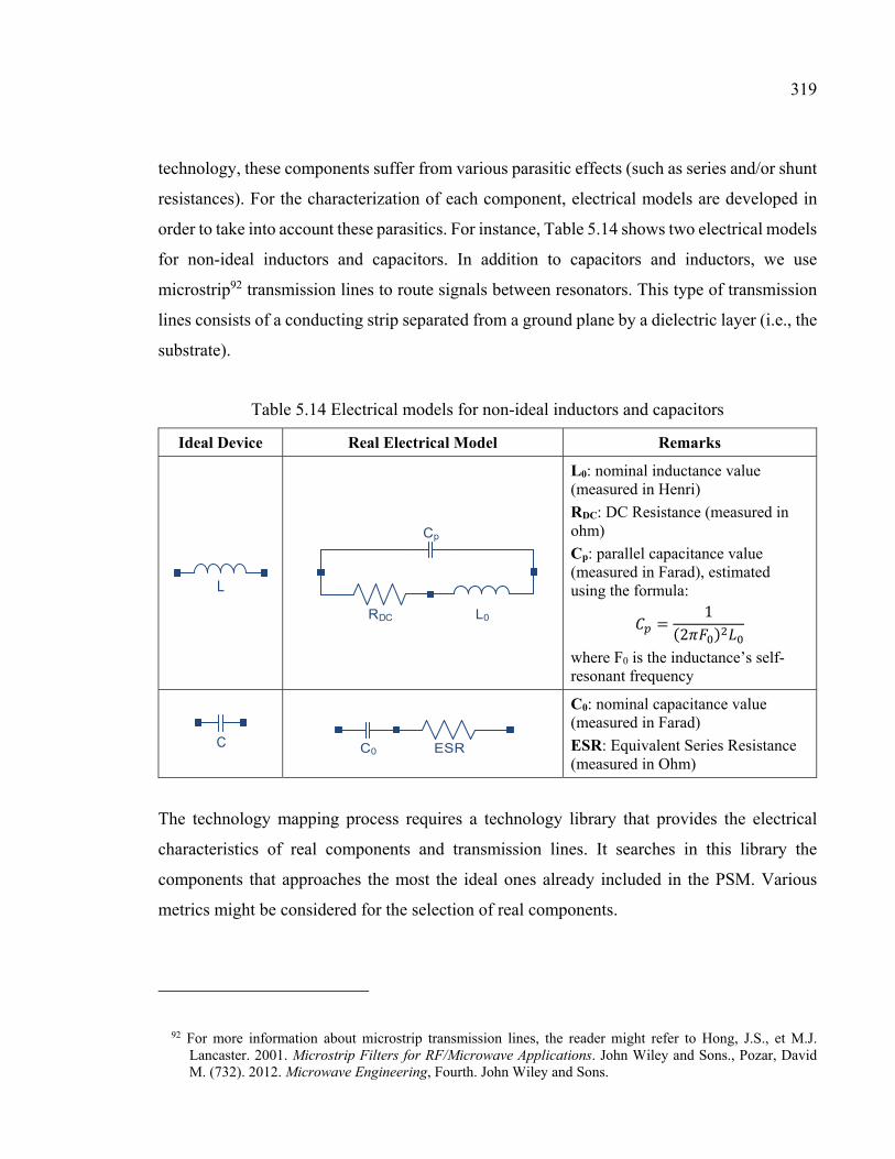
319
technology, these components suffer from various parasitic effects (such as series and/or shunt
resistances). For the characterization of each component, electrical models are developed in
order to take into account these parasitics. For instance, Table 5.14 shows two electrical models
for non-ideal inductors and capacitors. In addition to capacitors and inductors, we use
microstrip92 transmission lines to route signals between resonators. This type of transmission
lines consists of a conducting strip separated from a ground plane by a dielectric layer (i.e., the
substrate).
Table 5.14 Electrical models for non-ideal inductors and capacitors
Ideal Device Real Electrical Model Remarks
L
RDC
Cp
L0
L0: nominal inductance value (measured in Henri)
RDC: DC Resistance (measured in ohm)
Cp: parallel capacitance value (measured in Farad), estimated using the formula: = 1(2 )
where F0 is the inductance’s self-resonant frequency
C ESRC0
C0: nominal capacitance value (measured in Farad)
ESR: Equivalent Series Resistance (measured in Ohm)
The technology mapping process requires a technology library that provides the electrical
characteristics of real components and transmission lines. It searches in this library the
components that approaches the most the ideal ones already included in the PSM. Various
metrics might be considered for the selection of real components.
92 For more information about microstrip transmission lines, the reader might refer to Hong, J.S., et M.J. Lancaster. 2001. Microstrip Filters for RF/Microwave Applications. John Wiley and Sons., Pozar, David M. (732). 2012. Microwave Engineering, Fourth. John Wiley and Sons.
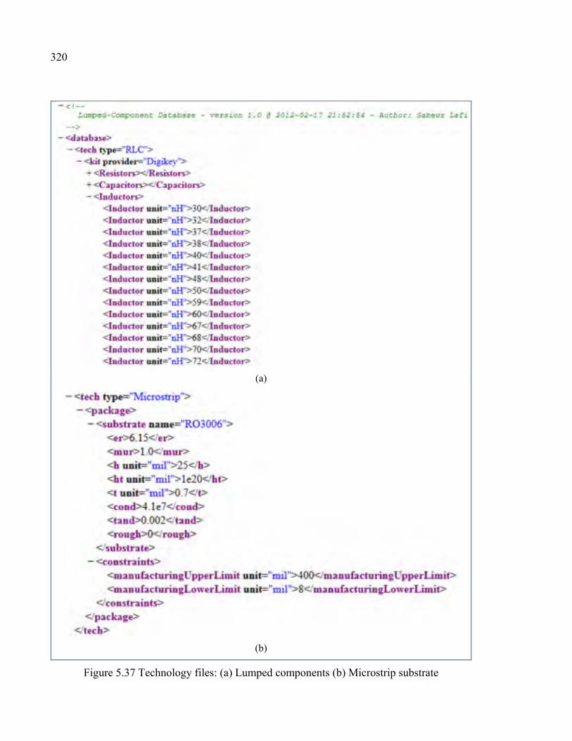
320
(a)
(b)
Figure 5.37 Technology files: (a) Lumped components (b) Microstrip substrate
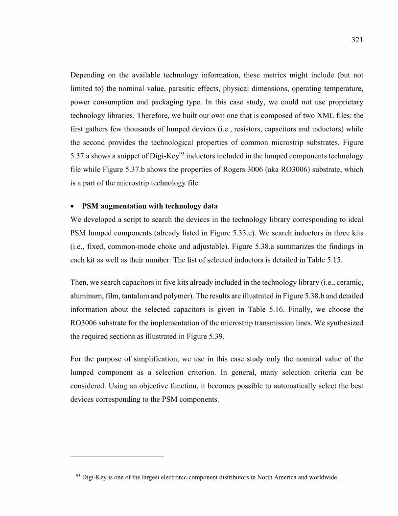
321
Depending on the available technology information, these metrics might include (but not
limited to) the nominal value, parasitic effects, physical dimensions, operating temperature,
power consumption and packaging type. In this case study, we could not use proprietary
technology libraries. Therefore, we built our own one that is composed of two XML files: the
first gathers few thousands of lumped devices (i.e., resistors, capacitors and inductors) while
the second provides the technological properties of common microstrip substrates. Figure
5.37.a shows a snippet of Digi-Key93 inductors included in the lumped components technology
file while Figure 5.37.b shows the properties of Rogers 3006 (aka RO3006) substrate, which
is a part of the microstrip technology file.
• PSM augmentation with technology data
We developed a script to search the devices in the technology library corresponding to ideal
PSM lumped components (already listed in Figure 5.33.c). We search inductors in three kits
(i.e., fixed, common-mode choke and adjustable). Figure 5.38.a summarizes the findings in
each kit as well as their number. The list of selected inductors is detailed in Table 5.15.
Then, we search capacitors in five kits already included in the technology library (i.e., ceramic,
aluminum, film, tantalum and polymer). The results are illustrated in Figure 5.38.b and detailed
information about the selected capacitors is given in Table 5.16. Finally, we choose the
RO3006 substrate for the implementation of the microstrip transmission lines. We synthesized
the required sections as illustrated in Figure 5.39.
For the purpose of simplification, we use in this case study only the nominal value of the
lumped component as a selection criterion. In general, many selection criteria can be
considered. Using an objective function, it becomes possible to automatically select the best
devices corresponding to the PSM components.
93 Digi-Key is one of the largest electronic-component distributors in North America and worldwide.
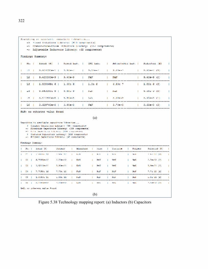
322
(a)
(b)
Figure 5.38 Technology mapping report: (a) Inductors (b) Capacitors
323
Figure 5. 39 Technology mapping report: Transmission lines synthesis
If quite detailed and complete technology libraries are available, the technology mapping
process contributes significantly to the automation of the design scheme. Concretely, this
process allows to:
− Bridge a gap in existent design tools: most popular commercial design packages do not
provide the automated selection of technology devices. Some design environments allow
the automated synthesis of distributed lines for limited number of circuits (e.g., planar
filters in Genesys and Microwave Office);
− Enable fully automated multi-criteria devices selection: given detailed characterization of
technology elements, objective functions can be used to select the best components fitting
to the PSM circuit;
324
− Operate in multi-technology design environment: the selection process does not only work
with lumped components. It is also possible to automatically synthesize complex planar
transmission lines, coaxial cables and multi-layer structures. Specialized tools can be used
to handle multi-technology issues (e.g., packaging, connections, discontinuities, etc.);
− Open the door for new types of analyses: the availability of detailed technology data
covering not only the electrical but also mechanical, environmental aspects, etc., which
enables to carry out different analyses uncommon at this abstraction level. In addition to
area estimation, other analyses such as power consumption, carbon fingerprint, and heat
dissipation can take place.
In addition, the use of standard formats (such as XML) for technology libraries instead of the
prevalent proprietary file formats is another provision that enhances data exchange and
communication between concurrent design environments.
i) Synthesis: PSM performance assessment and optimization
During technology mapping, we choose the real capacitors and inductors to replace ideal PSM
lumped components (see the row entitled “selected?” in Table 5.15 and Table 5.16). We have
also synthesized the microstrip sections to connect the lumped devices as well as the suitable
via holes to ensure ground connectivity. The resulting circuit PSM schematic is shown in
Figure 5.33.c.
After linear simulation, we illustrate its frequency response in Figure 5.40. It is obvious that
the PSM’s overall performance has decreased if compared to the ideal PSM frequency response
of Figure 5.36. The reason behind this performance degradation is not only due to the small
difference in nominal values between ideal and non-ideal lumped devices but also caused by
their parasitic effects as well as the imperfections of microstrip sections (e.g., the effect of
discontinuities, fringing fields, via holes, substrate, etc.).
To meet the requirements, we carried out several optimization iterations in order to minimize
the effects due to the imperfections of lumped devices and microstrip sections. We succeed to
find out two PSM configurations that meet the requirements. The first is characterized by a
relatively constant group delay over a wide range of frequencies but it suffers from a disturbed

325
roll-off in the upper transition band (see Figure 5.41). The second design solution shows
interesting reflection and transmission characteristics (see Figure 5.42). We use both candidate
solutions to generate two distinct PMs in the next design stage.
It is worth noting that if the optimization effort fails at this step in the search of a PSM that
meets the initial requirements, a design re-spin becomes inevitable. Thus, the design will restart
at the step of PSM granularity refinement in the purpose of figuring out a new design solution.
The new PSM is submitted again to technology mapping and performance assessment
respectively.
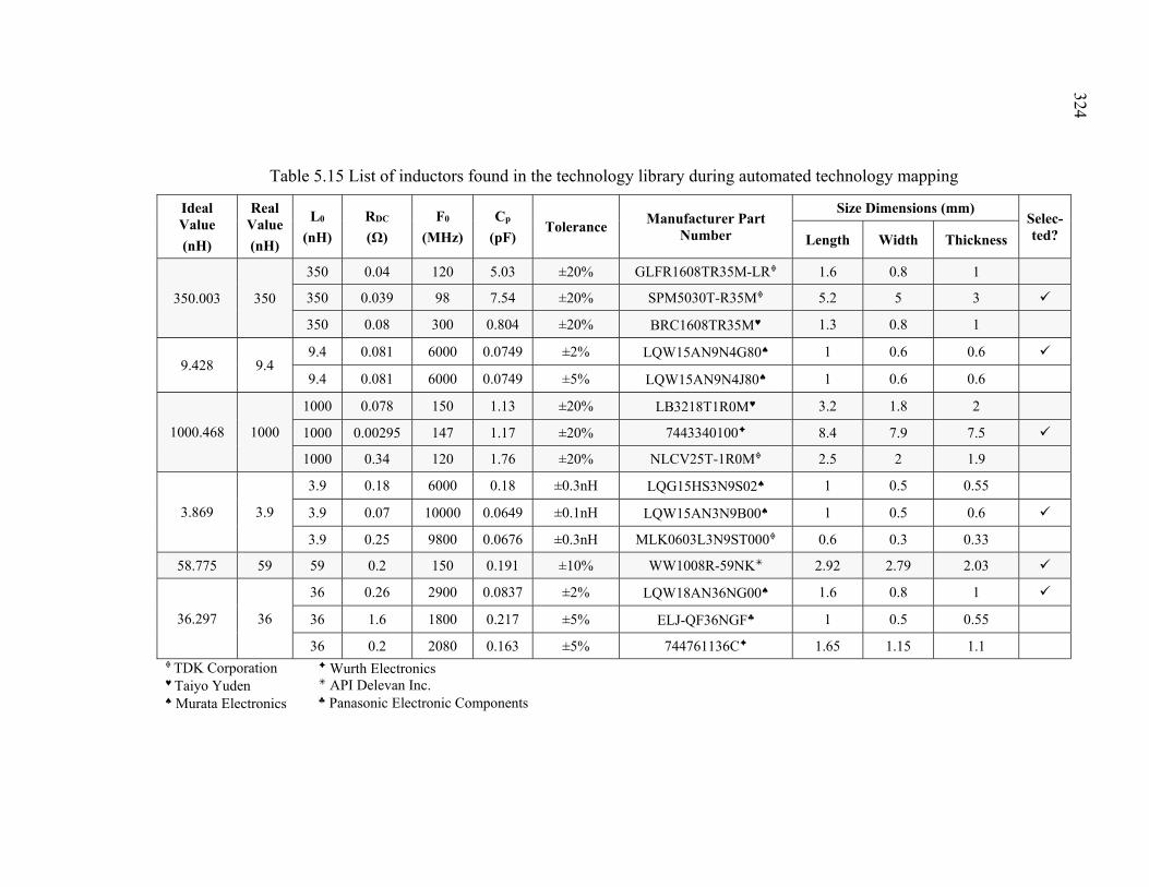
Table 5.15 List of inductors found in the technology library during automated technology mapping
Ideal Value
(nH)
Real Value
(nH)
L0
(nH)
RDC
(Ω)
F0
(MHz)
Cp
(pF) Tolerance
Manufacturer Part Number
Size Dimensions (mm) Selec-ted? Length Width Thickness
350.003 350
350 0.04 120 5.03 ±20% GLFR1608TR35M-LR 1.6 0.8 1
350 0.039 98 7.54 ±20% SPM5030T-R35M 5.2 5 3
350 0.08 300 0.804 ±20% BRC1608TR35M♥ 1.3 0.8 1
9.428 9.4 9.4 0.081 6000 0.0749 ±2% LQW15AN9N4G80♠ 1 0.6 0.6
9.4 0.081 6000 0.0749 ±5% LQW15AN9N4J80♠ 1 0.6 0.6
1000.468 1000
1000 0.078 150 1.13 ±20% LB3218T1R0M♥ 3.2 1.8 2
1000 0.00295 147 1.17 ±20% 7443340100 8.4 7.9 7.5
1000 0.34 120 1.76 ±20% NLCV25T-1R0M 2.5 2 1.9
3.869 3.9
3.9 0.18 6000 0.18 ±0.3nH LQG15HS3N9S02♠ 1 0.5 0.55
3.9 0.07 10000 0.0649 ±0.1nH LQW15AN3N9B00♠ 1 0.5 0.6
3.9 0.25 9800 0.0676 ±0.3nH MLK0603L3N9ST000 0.6 0.3 0.33
58.775 59 59 0.2 150 0.191 ±10% WW1008R-59NK 2.92 2.79 2.03
36.297 36
36 0.26 2900 0.0837 ±2% LQW18AN36NG00♠ 1.6 0.8 1
36 1.6 1800 0.217 ±5% ELJ-QF36NGF♣ 1 0.5 0.55
36 0.2 2080 0.163 ±5% 744761136C 1.65 1.15 1.1 TDK Corporation ♥ Taiyo Yuden ♠ Murata Electronics
Wurth Electronics API Delevan Inc. ♣ Panasonic Electronic Components
324
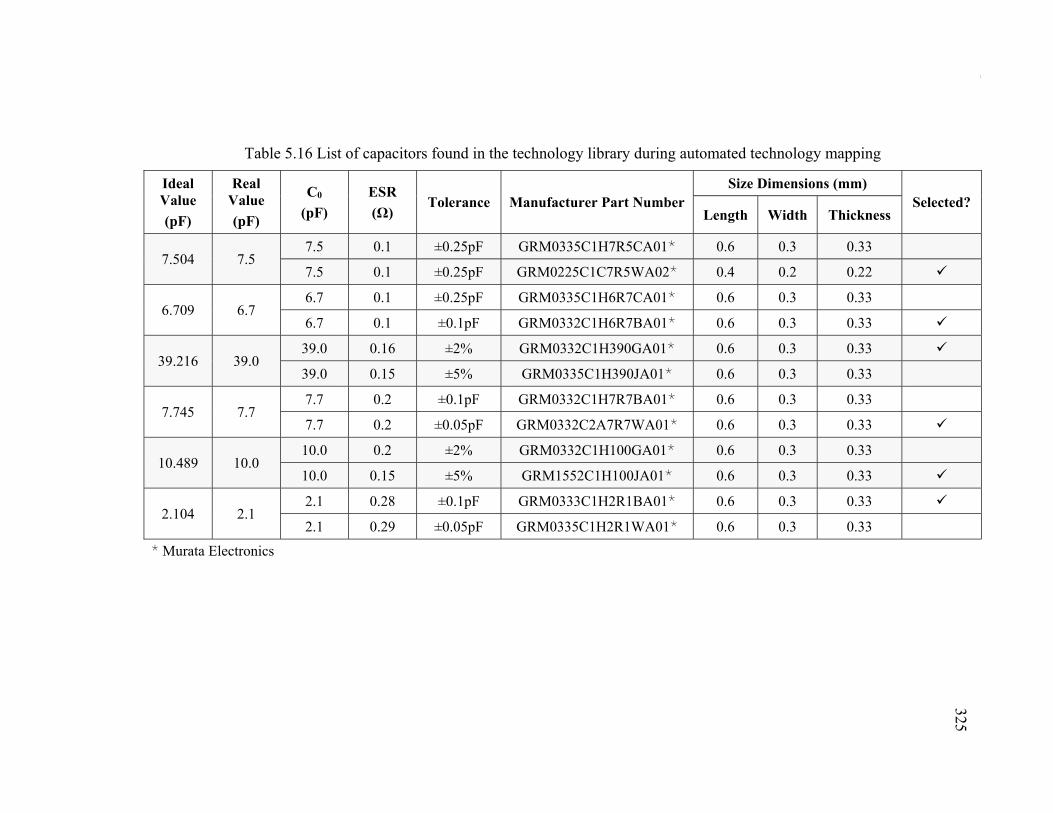
327
Table 5.16 List of capacitors found in the technology library during automated technology mapping
Ideal Value
(pF)
Real Value
(pF)
C0
(pF)
ESR
(Ω) Tolerance Manufacturer Part Number
Size Dimensions (mm) Selected?
Length Width Thickness
7.504 7.5 7.5 0.1 ±0.25pF GRM0335C1H7R5CA01 0.6 0.3 0.33
7.5 0.1 ±0.25pF GRM0225C1C7R5WA02 0.4 0.2 0.22
6.709 6.7 6.7 0.1 ±0.25pF GRM0335C1H6R7CA01 0.6 0.3 0.33
6.7 0.1 ±0.1pF GRM0332C1H6R7BA01 0.6 0.3 0.33
39.216 39.0 39.0 0.16 ±2% GRM0332C1H390GA01 0.6 0.3 0.33
39.0 0.15 ±5% GRM0335C1H390JA01 0.6 0.3 0.33
7.745 7.7 7.7 0.2 ±0.1pF GRM0332C1H7R7BA01 0.6 0.3 0.33
7.7 0.2 ±0.05pF GRM0332C2A7R7WA01 0.6 0.3 0.33
10.489 10.0 10.0 0.2 ±2% GRM0332C1H100GA01 0.6 0.3 0.33
10.0 0.15 ±5% GRM1552C1H100JA01 0.6 0.3 0.33
2.104 2.1 2.1 0.28 ±0.1pF GRM0333C1H2R1BA01 0.6 0.3 0.33
2.1 0.29 ±0.05pF GRM0335C1H2R1WA01 0.6 0.3 0.33 Murata Electronics
325
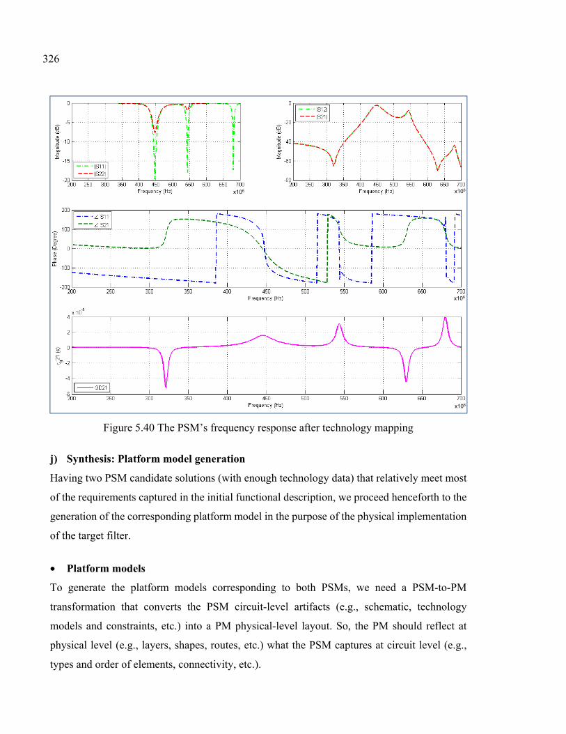
Figure 5.40 The PSM’s frequency response after technology mapping
j) Synthesis: Platform model generation
Having two PSM candidate solutions (with enough technology data) that relatively meet most
of the requirements captured in the initial functional description, we proceed henceforth to the
generation of the corresponding platform model in the purpose of the physical implementation
of the target filter.
• Platform models
To generate the platform models corresponding to both PSMs, we need a PSM-to-PM
transformation that converts the PSM circuit-level artifacts (e.g., schematic, technology
models and constraints, etc.) into a PM physical-level layout. So, the PM should reflect at
physical level (e.g., layers, shapes, routes, etc.) what the PSM captures at circuit level (e.g.,
types and order of elements, connectivity, etc.).
326
x106 x106
x106
x106
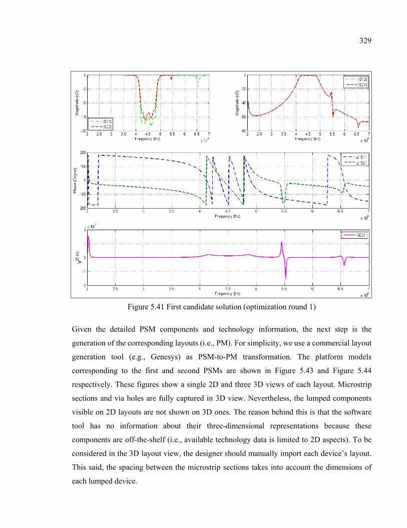
329
Figure 5.41 First candidate solution (optimization round 1)
Given the detailed PSM components and technology information, the next step is the
generation of the corresponding layouts (i.e., PM). For simplicity, we use a commercial layout
generation tool (e.g., Genesys) as PSM-to-PM transformation. The platform models
corresponding to the first and second PSMs are shown in Figure 5.43 and Figure 5.44
respectively. These figures show a single 2D and three 3D views of each layout. Microstrip
sections and via holes are fully captured in 3D view. Nevertheless, the lumped components
visible on 2D layouts are not shown on 3D ones. The reason behind this is that the software
tool has no information about their three-dimensional representations because these
components are off-the-shelf (i.e., available technology data is limited to 2D aspects). To be
considered in the 3D layout view, the designer should manually import each device’s layout.
This said, the spacing between the microstrip sections takes into account the dimensions of
each lumped device.
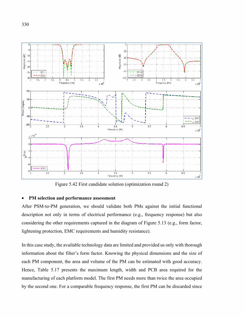
330
Figure 5.42 First candidate solution (optimization round 2)
• PM selection and performance assessment
After PSM-to-PM generation, we should validate both PMs against the initial functional
description not only in terms of electrical performance (e.g., frequency response) but also
considering the other requirements captured in the diagram of Figure 5.13 (e.g., form factor,
lightening protection, EMC requirements and humidity resistance).
In this case study, the available technology data are limited and provided us only with thorough
information about the filter’s form factor. Knowing the physical dimensions and the size of
each PM component, the area and volume of the PM can be estimated with good accuracy.
Hence, Table 5.17 presents the maximum length, width and PCB area required for the
manufacturing of each platform model. The first PM needs more than twice the area occupied
by the second one. For a comparable frequency response, the first PM can be discarded since
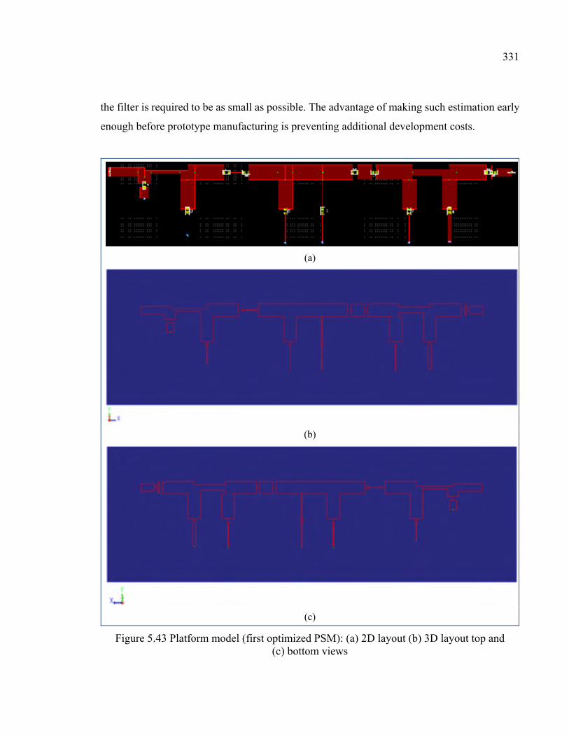
331
the filter is required to be as small as possible. The advantage of making such estimation early
enough before prototype manufacturing is preventing additional development costs.
(a)
(b)
(c)
Figure 5.43 Platform model (first optimized PSM): (a) 2D layout (b) 3D layout top and (c) bottom views
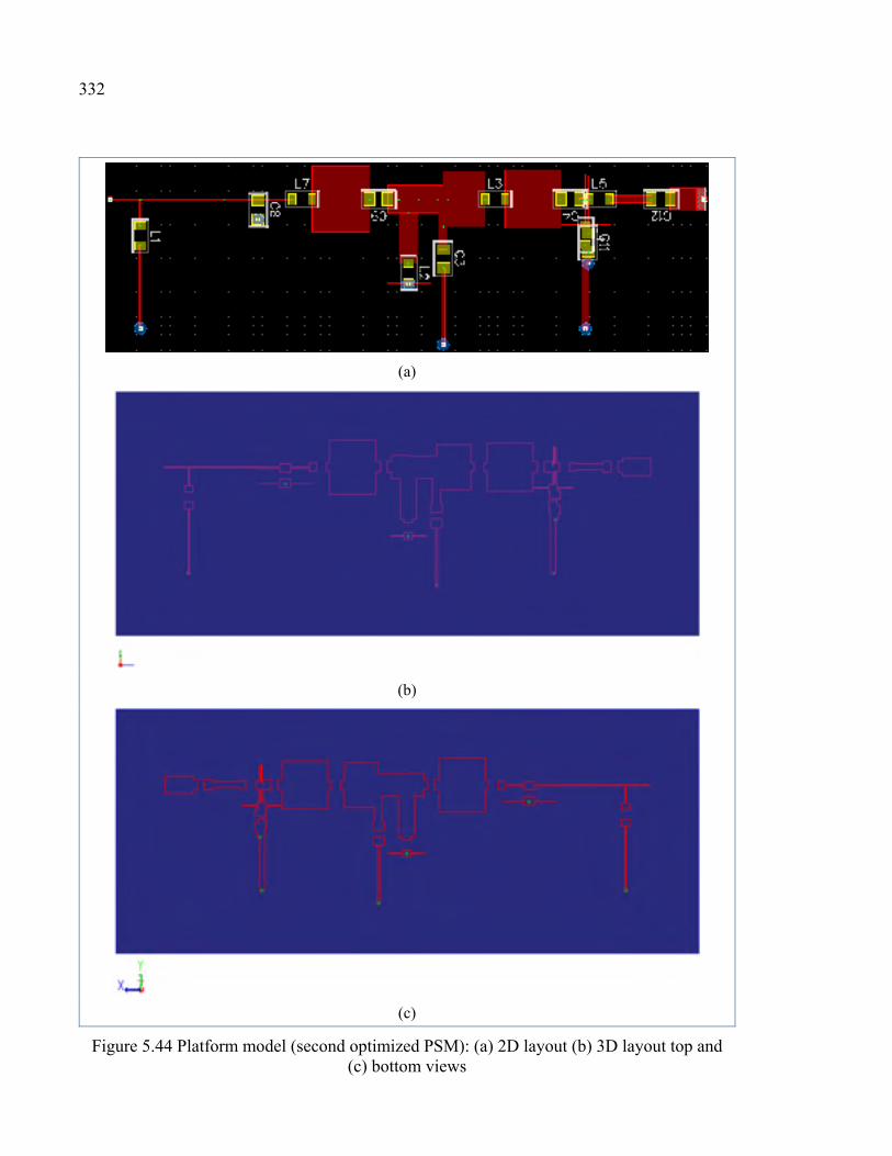
332
(a)
(b)
(c)
Figure 5.44 Platform model (second optimized PSM): (a) 2D layout (b) 3D layout top and (c) bottom views
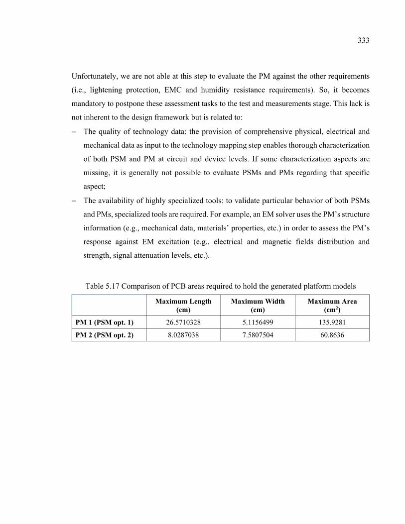
333
Unfortunately, we are not able at this step to evaluate the PM against the other requirements
(i.e., lightening protection, EMC and humidity resistance requirements). So, it becomes
mandatory to postpone these assessment tasks to the test and measurements stage. This lack is
not inherent to the design framework but is related to:
− The quality of technology data: the provision of comprehensive physical, electrical and
mechanical data as input to the technology mapping step enables thorough characterization
of both PSM and PM at circuit and device levels. If some characterization aspects are
missing, it is generally not possible to evaluate PSMs and PMs regarding that specific
aspect;
− The availability of highly specialized tools: to validate particular behavior of both PSMs
and PMs, specialized tools are required. For example, an EM solver uses the PM’s structure
information (e.g., mechanical data, materials’ properties, etc.) in order to assess the PM’s
response against EM excitation (e.g., electrical and magnetic fields distribution and
strength, signal attenuation levels, etc.).
Table 5.17 Comparison of PCB areas required to hold the generated platform models
Maximum Length
(cm) Maximum Width
(cm) Maximum Area
(cm2)
PM 1 (PSM opt. 1) 26.5710328 5.1156499 135.9281
PM 2 (PSM opt. 2) 8.0287038 7.5807504 60.8636
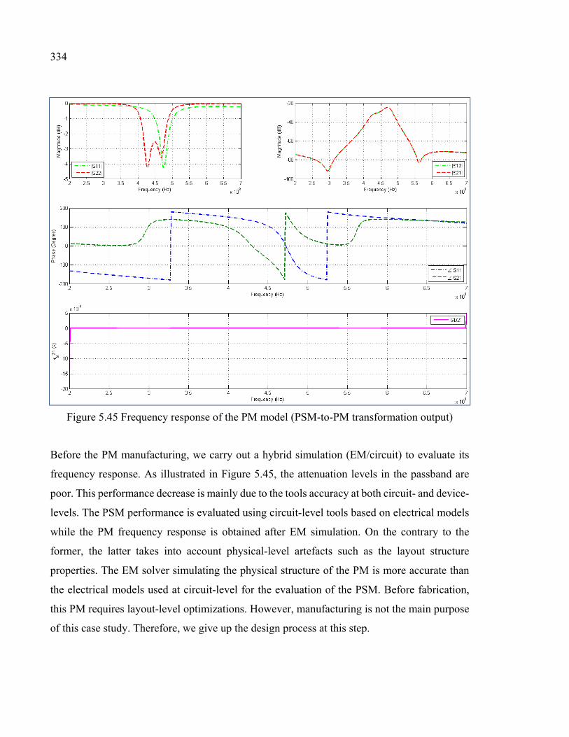
334
Figure 5.45 Frequency response of the PM model (PSM-to-PM transformation output)
Before the PM manufacturing, we carry out a hybrid simulation (EM/circuit) to evaluate its
frequency response. As illustrated in Figure 5.45, the attenuation levels in the passband are
poor. This performance decrease is mainly due to the tools accuracy at both circuit- and device-
levels. The PSM performance is evaluated using circuit-level tools based on electrical models
while the PM frequency response is obtained after EM simulation. On the contrary to the
former, the latter takes into account physical-level artefacts such as the layout structure
properties. The EM solver simulating the physical structure of the PM is more accurate than
the electrical models used at circuit-level for the evaluation of the PSM. Before fabrication,
this PM requires layout-level optimizations. However, manufacturing is not the main purpose
of this case study. Therefore, we give up the design process at this step.
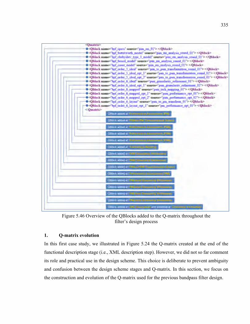
335
Figure 5.46 Overview of the QBlocks added to the Q-matrix throughout the filter’s design process
1. Q-matrix evolution
In this first case study, we illustrated in Figure 5.24 the Q-matrix created at the end of the
functional description stage (i.e., XML description step). However, we did not so far comment
its role and practical use in the design scheme. This choice is deliberate to prevent ambiguity
and confusion between the design scheme stages and Q-matrix. In this section, we focus on
the construction and evolution of the Q-matrix used for the previous bandpass filter design.
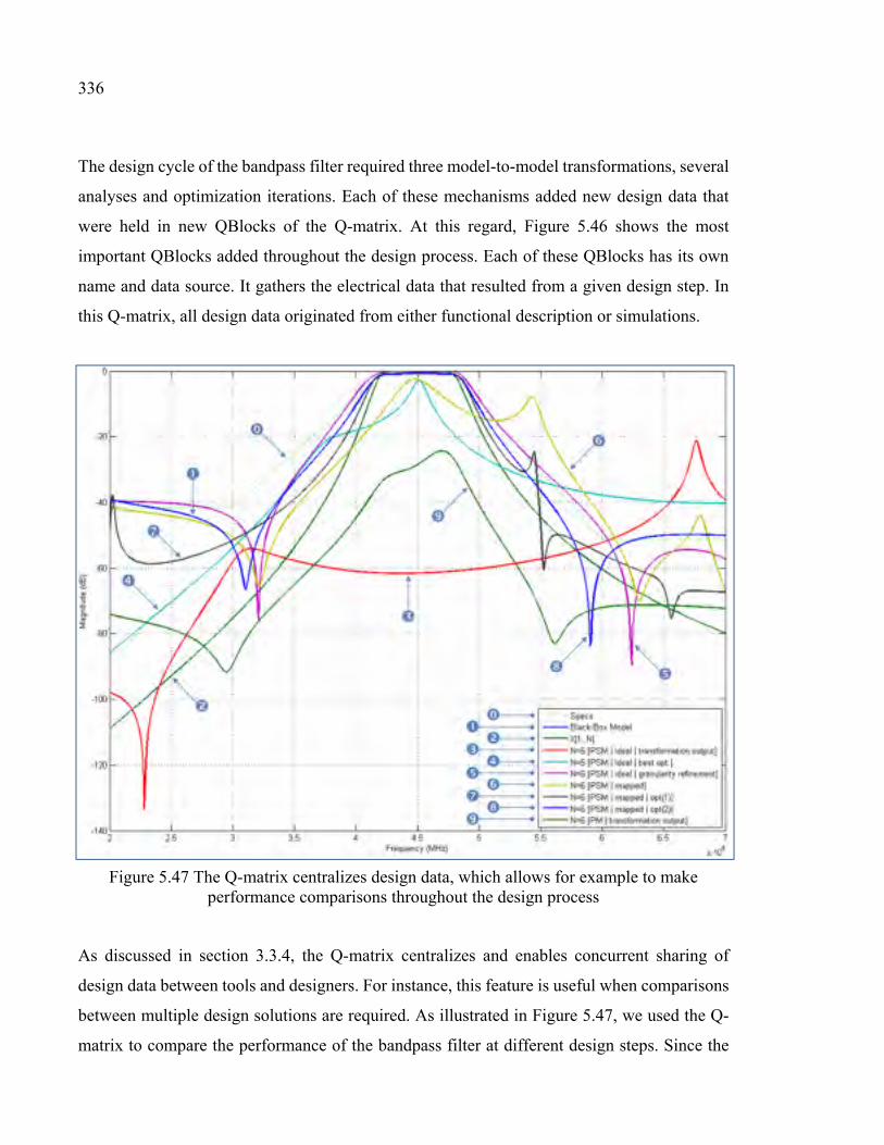
336
The design cycle of the bandpass filter required three model-to-model transformations, several
analyses and optimization iterations. Each of these mechanisms added new design data that
were held in new QBlocks of the Q-matrix. At this regard, Figure 5.46 shows the most
important QBlocks added throughout the design process. Each of these QBlocks has its own
name and data source. It gathers the electrical data that resulted from a given design step. In
this Q-matrix, all design data originated from either functional description or simulations.
Figure 5.47 The Q-matrix centralizes design data, which allows for example to make performance comparisons throughout the design process
As discussed in section 3.3.4, the Q-matrix centralizes and enables concurrent sharing of
design data between tools and designers. For instance, this feature is useful when comparisons
between multiple design solutions are required. As illustrated in Figure 5.47, we used the Q-
matrix to compare the performance of the bandpass filter at different design steps. Since the
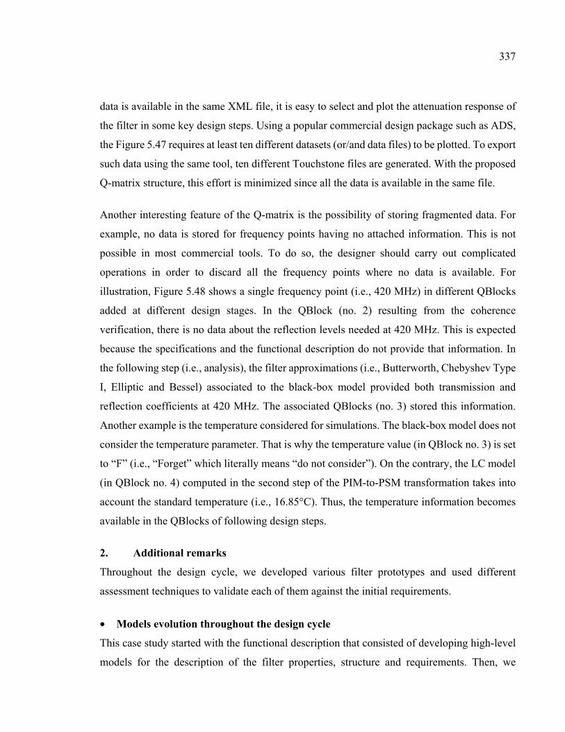
337
data is available in the same XML file, it is easy to select and plot the attenuation response of
the filter in some key design steps. Using a popular commercial design package such as ADS,
the Figure 5.47 requires at least ten different datasets (or/and data files) to be plotted. To export
such data using the same tool, ten different Touchstone files are generated. With the proposed
Q-matrix structure, this effort is minimized since all the data is available in the same file.
Another interesting feature of the Q-matrix is the possibility of storing fragmented data. For
example, no data is stored for frequency points having no attached information. This is not
possible in most commercial tools. To do so, the designer should carry out complicated
operations in order to discard all the frequency points where no data is available. For
illustration, Figure 5.48 shows a single frequency point (i.e., 420 MHz) in different QBlocks
added at different design stages. In the QBlock (no. 2) resulting from the coherence
verification, there is no data about the reflection levels needed at 420 MHz. This is expected
because the specifications and the functional description do not provide that information. In
the following step (i.e., analysis), the filter approximations (i.e., Butterworth, Chebyshev Type
I, Elliptic and Bessel) associated to the black-box model provided both transmission and
reflection coefficients at 420 MHz. The associated QBlocks (no. 3) stored this information.
Another example is the temperature considered for simulations. The black-box model does not
consider the temperature parameter. That is why the temperature value (in QBlock no. 3) is set
to “F” (i.e., “Forget” which literally means “do not consider”). On the contrary, the LC model
(in QBlock no. 4) computed in the second step of the PIM-to-PSM transformation takes into
account the standard temperature (i.e., 16.85°C). Thus, the temperature information becomes
available in the QBlocks of following design steps.
2. Additional remarks
Throughout the design cycle, we developed various filter prototypes and used different
assessment techniques to validate each of them against the initial requirements.
• Models evolution throughout the design cycle
This case study started with the functional description that consisted of developing high-level
models for the description of the filter properties, structure and requirements. Then, we
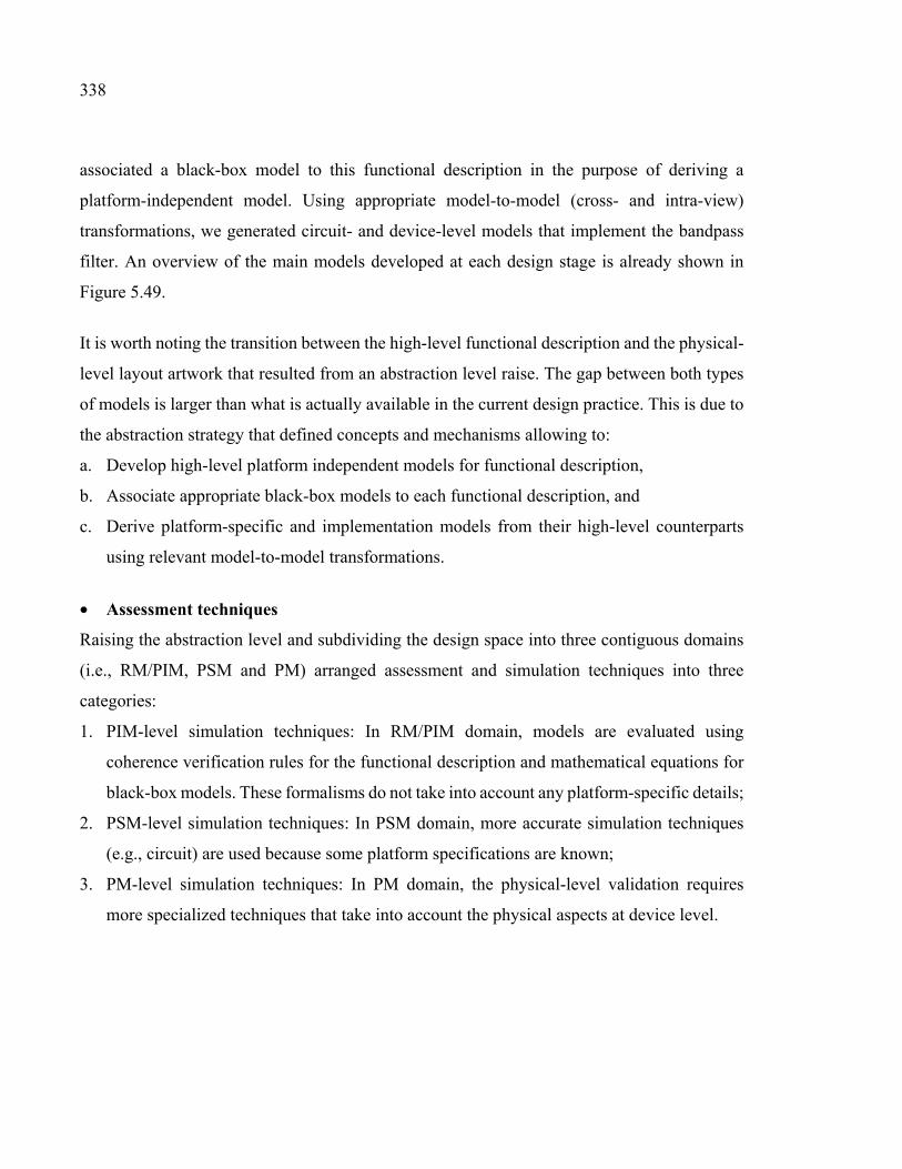
338
associated a black-box model to this functional description in the purpose of deriving a
platform-independent model. Using appropriate model-to-model (cross- and intra-view)
transformations, we generated circuit- and device-level models that implement the bandpass
filter. An overview of the main models developed at each design stage is already shown in
Figure 5.49.
It is worth noting the transition between the high-level functional description and the physical-
level layout artwork that resulted from an abstraction level raise. The gap between both types
of models is larger than what is actually available in the current design practice. This is due to
the abstraction strategy that defined concepts and mechanisms allowing to:
a. Develop high-level platform independent models for functional description,
b. Associate appropriate black-box models to each functional description, and
c. Derive platform-specific and implementation models from their high-level counterparts
using relevant model-to-model transformations.
• Assessment techniques
Raising the abstraction level and subdividing the design space into three contiguous domains
(i.e., RM/PIM, PSM and PM) arranged assessment and simulation techniques into three
categories:
1. PIM-level simulation techniques: In RM/PIM domain, models are evaluated using
coherence verification rules for the functional description and mathematical equations for
black-box models. These formalisms do not take into account any platform-specific details;
2. PSM-level simulation techniques: In PSM domain, more accurate simulation techniques
(e.g., circuit) are used because some platform specifications are known;
3. PM-level simulation techniques: In PM domain, the physical-level validation requires
more specialized techniques that take into account the physical aspects at device level.
Figure 5.48 An overview of Q-matrix QBlocks evolution throughout the design cycle
339
340
Figure 5.49 The evolution of the filter models throughout the design cycle
340
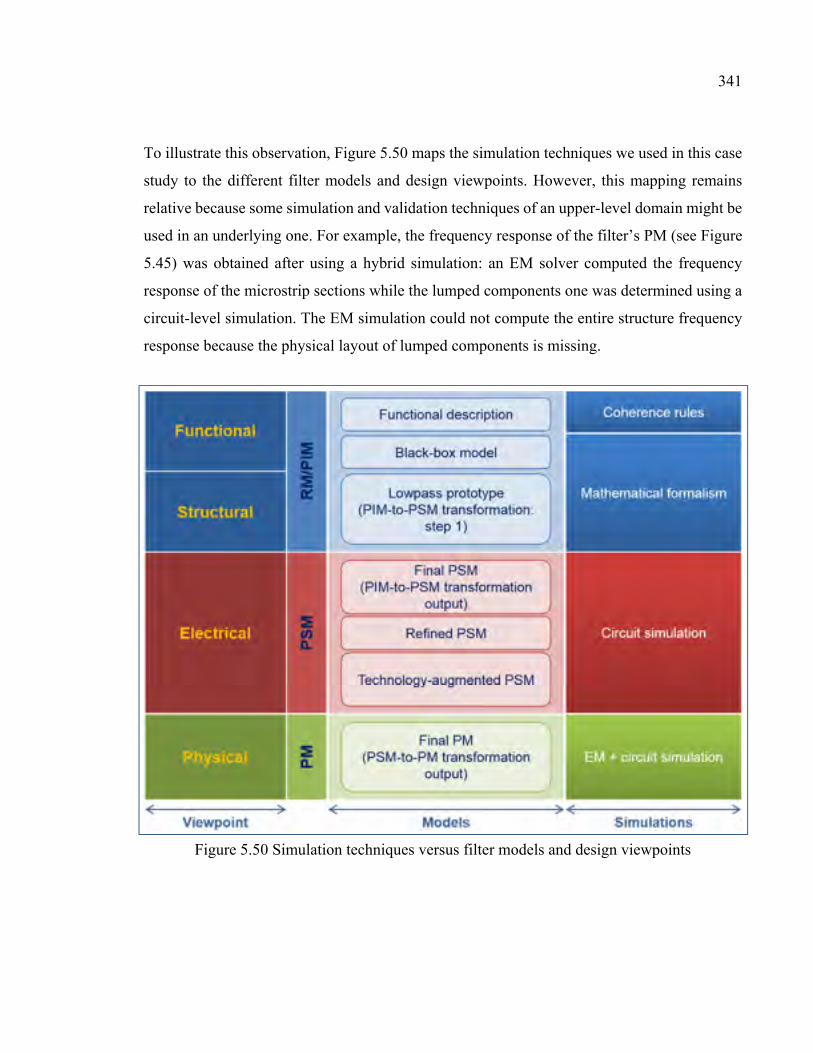
341
To illustrate this observation, Figure 5.50 maps the simulation techniques we used in this case
study to the different filter models and design viewpoints. However, this mapping remains
relative because some simulation and validation techniques of an upper-level domain might be
used in an underlying one. For example, the frequency response of the filter’s PM (see Figure
5.45) was obtained after using a hybrid simulation: an EM solver computed the frequency
response of the microstrip sections while the lumped components one was determined using a
circuit-level simulation. The EM simulation could not compute the entire structure frequency
response because the physical layout of lumped components is missing.
Figure 5.50 Simulation techniques versus filter models and design viewpoints
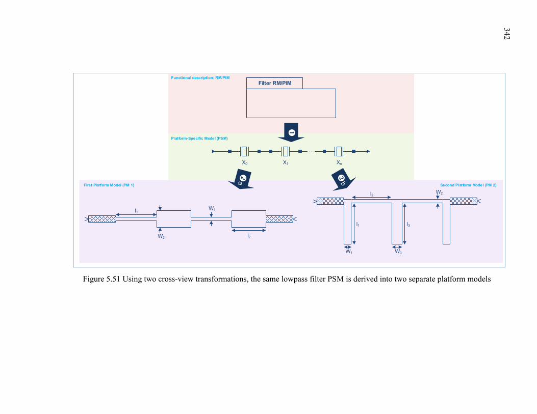
l1
W2 l2
W1
Filter RM/PIM
...
X0 X1 Xn
Functional description: RM/PIM
First Platform Model (PM 1) Second Platform Model (PM 2)
Platform-Specific Model (PSM)
l2 W2
W3
l1 l3
W1
Figure 5.51 Using two cross-view transformations, the same lowpass filter PSM is derived into two separate platform models
342
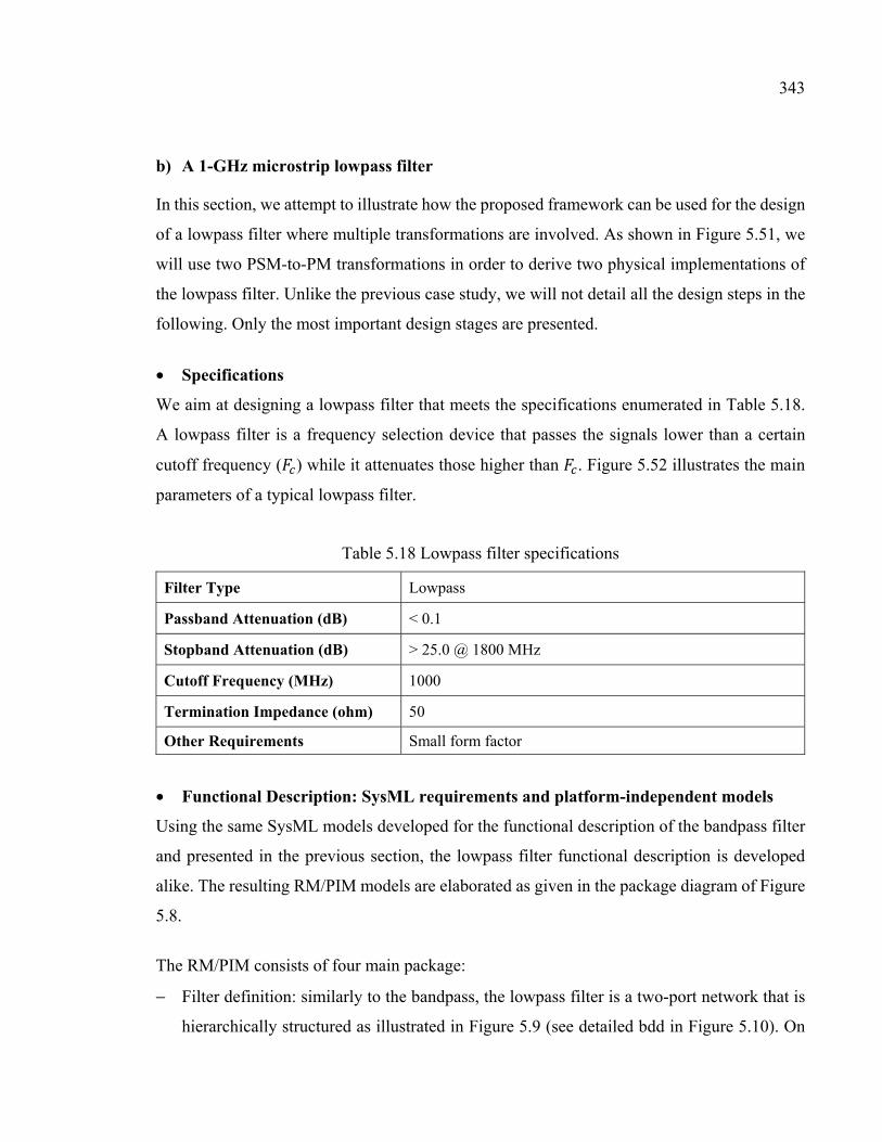
343
b) A 1-GHz microstrip lowpass filter
In this section, we attempt to illustrate how the proposed framework can be used for the design
of a lowpass filter where multiple transformations are involved. As shown in Figure 5.51, we
will use two PSM-to-PM transformations in order to derive two physical implementations of
the lowpass filter. Unlike the previous case study, we will not detail all the design steps in the
following. Only the most important design stages are presented.
• Specifications
We aim at designing a lowpass filter that meets the specifications enumerated in Table 5.18.
A lowpass filter is a frequency selection device that passes the signals lower than a certain
cutoff frequency ( ) while it attenuates those higher than . Figure 5.52 illustrates the main
parameters of a typical lowpass filter.
Table 5.18 Lowpass filter specifications
Filter Type Lowpass
Passband Attenuation (dB) < 0.1
Stopband Attenuation (dB) > 25.0 @ 1800 MHz
Cutoff Frequency (MHz) 1000
Termination Impedance (ohm) 50
Other Requirements Small form factor
• Functional Description: SysML requirements and platform-independent models
Using the same SysML models developed for the functional description of the bandpass filter
and presented in the previous section, the lowpass filter functional description is developed
alike. The resulting RM/PIM models are elaborated as given in the package diagram of Figure
5.8.
The RM/PIM consists of four main package:
− Filter definition: similarly to the bandpass, the lowpass filter is a two-port network that is
hierarchically structured as illustrated in Figure 5.9 (see detailed bdd in Figure 5.10). On
344
the contrary to the bandpass, the lowpass device is a single-side filter. Thus, it inherits the
properties of a single-side instead of a mid-band filter (see Figure 5.11). This difference is
illustrated in Table 5.19 where the properties “centerFrequency” and “bandwidth” are
replaced by their counterparts “cutoffFrequency” and “stopbandEdgeFrequency” (see
gray-colored rows in Table 5.19). In addition, the value property belonging to the bandpass
bdd, namely “fractionalBandwidth” is ignored in the lowpass case because it is has no
definition;
− Filter requirements: the lowpass requirements include performance and form factor
specifications (see requirement diagram of Figure 5.49);
− Filter coherence rules: the lowpass coherent rules consist of the PIM-level design
constraints, the electrical consistence rules, and the integrity control rules. The first rules
are the same as for the bandpass filter while the second and the third ones are slightly
different.
• Analysis: Coherence verification
As previously mentioned, the lowpass filter functional description include three types of
coherence rules:
1. PIM-level design constraints: are the same as in Table 5.7;
2. Electrical consistence rules: include two sets of rules. The first is represented in the
parameters relationships graph of Figure 5.54 and the corresponding equations are
enumerated in Table 5.20. The second set consists of equations E.1 and E.2 of Table 5.6;
3. Integrity control rules: include the rules I.1 through I.32 of Table 5.8. The rules I.34 and
I.35 are used only with mid-band (such as bandpass filters).
The functional description elaborated in the previous steps is checked using the coherence
verification rules. The resulting coherence verification report is given in Figure 5.55.
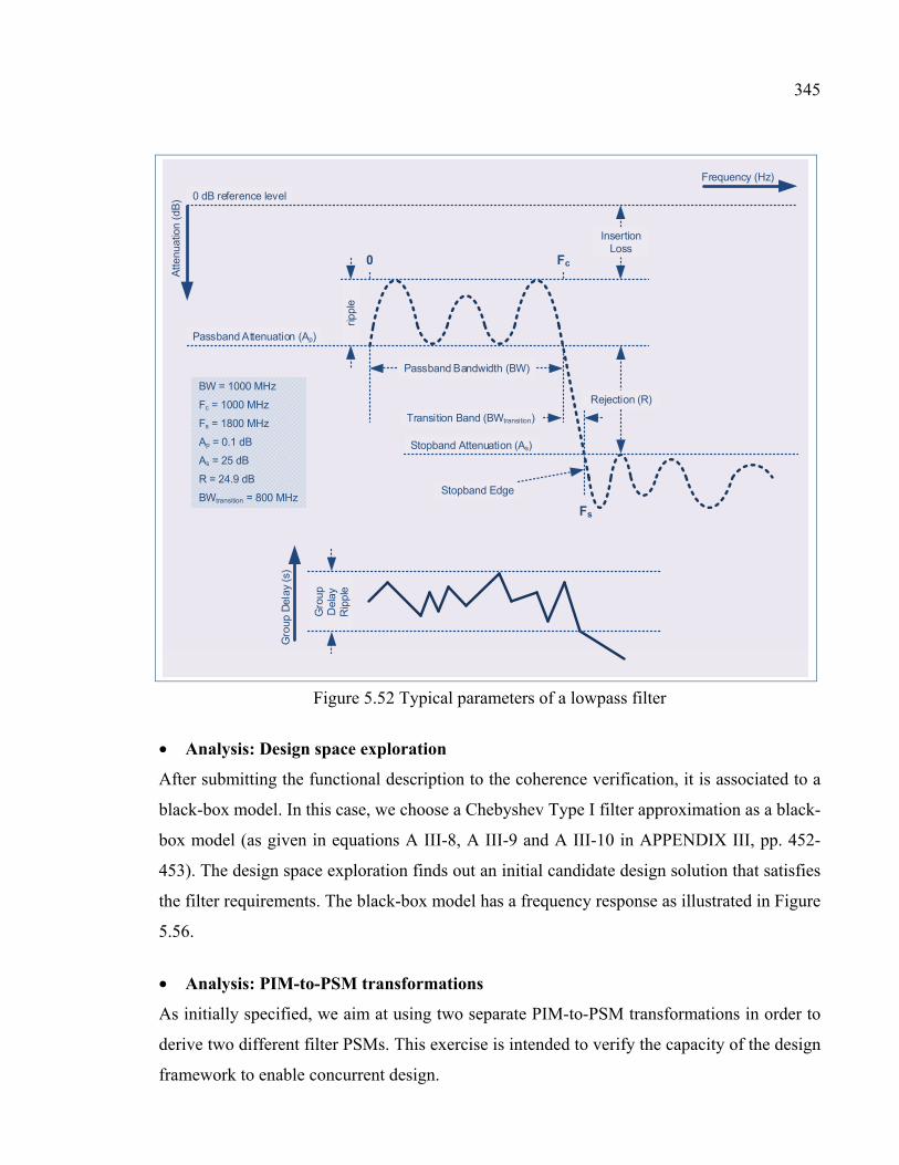
345
Gro
up
Del
ay
Rip
ple
Stopband Attenuation (As)
Passband Attenuation (Ap)
0 dB reference level
rippl
e
Insertion Loss
Rejection (R)
Passband Bandwidth (BW)
Stopband Edge
Fs
0 Fc
Transition Band (BWtransition)
Atte
nuat
ion
(dB
)Frequency (Hz)
BW = 1000 MHz
Fc = 1000 MHz
Fs = 1800 MHz
Ap = 0.1 dB
As = 25 dB
R = 24.9 dB
BWtransition = 800 MHz
Gro
up D
elay
(s)
Figure 5.52 Typical parameters of a lowpass filter
• Analysis: Design space exploration
After submitting the functional description to the coherence verification, it is associated to a
black-box model. In this case, we choose a Chebyshev Type I filter approximation as a black-
box model (as given in equations A III-8, A III-9 and A III-10 in APPENDIX III, pp. 452-
453). The design space exploration finds out an initial candidate design solution that satisfies
the filter requirements. The black-box model has a frequency response as illustrated in Figure
5.56.
• Analysis: PIM-to-PSM transformations
As initially specified, we aim at using two separate PIM-to-PSM transformations in order to
derive two different filter PSMs. This exercise is intended to verify the capacity of the design
framework to enable concurrent design.
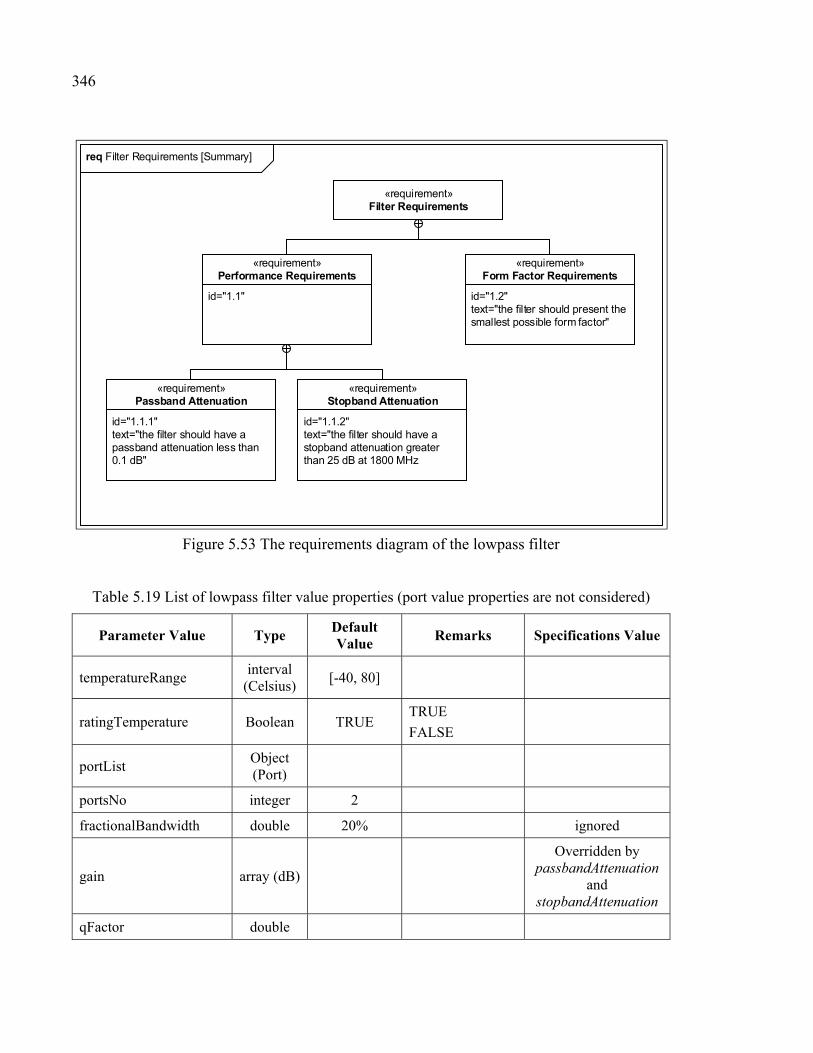
346
req Filter Requirements [Summary]
«requirement»Filter Requirements
id="1.2"text="the filter should present the smallest possible form factor"
«requirement»Form Factor Requirements
id="1.1.1"text="the filter should have a passband attenuation less than 0.1 dB"
«requirement»Passband Attenuation
id="1.1.2"text="the filter should have a stopband attenuation greater than 25 dB at 1800 MHz
«requirement»Stopband Attenuation
id="1.1"
«requirement»Performance Requirements
Figure 5.53 The requirements diagram of the lowpass filter
Table 5.19 List of lowpass filter value properties (port value properties are not considered)
Parameter Value Type Default Value
Remarks Specifications Value
temperatureRange interval
(Celsius) [-40, 80]
ratingTemperature Boolean TRUE TRUE
FALSE
portList Object (Port)
portsNo integer 2
fractionalBandwidth double 20% ignored
gain array (dB)
Overridden by passbandAttenuation
and stopbandAttenuation
qFactor double
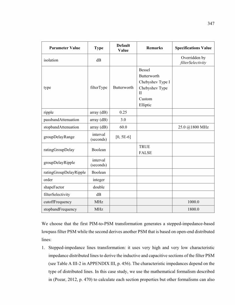
347
Parameter Value Type Default Value
Remarks Specifications Value
isolation dB Overridden by filterSelectivity
type filterType Butterworth
Bessel
Butterworth
Chebyshev Type I
Chebyshev Type II
Custom
Elliptic
ripple array (dB) 0.25
passbandAttenuation array (dB) 3.0
stopbandAttenuation array (dB) 60.0 25.0 @1800 MHz
groupDelayRange interval
(seconds) [0, 5E-6]
ratingGroupDelay Boolean TRUE
FALSE
groupDelayRipple interval
(seconds)
ratingGroupDelayRipple Boolean
order integer
shapeFactor double
filterSelectivity dB
cutoffFrequency MHz 1000.0
stopbandFrequency MHz 1800.0
We choose that the first PIM-to-PSM transformation generates a stepped-impedance-based
lowpass filter PSM while the second derives another PSM that is based on open-end distributed
lines:
1. Stepped-impedance lines transformation: it uses very high and very low characteristic
impedance distributed lines to derive the inductive and capacitive sections of the filter PSM
(see Table A III-2 in APPENDIX III, p. 456). The characteristic impedances depend on the
type of distributed lines. In this case study, we use the mathematical formalism described
in (Pozar, 2012, p. 470) to calculate each section properties but other formalisms can also
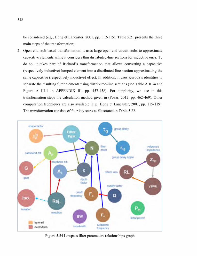
348
be considered (e.g., Hong et Lancaster, 2001, pp. 112-115). Table 5.21 presents the three
main steps of the transformation;
2. Open-end stub-based transformation: it uses large open-end circuit stubs to approximate
capacitive elements while it considers thin distributed-line sections for inductive ones. To
do so, it takes part of Richard’s transformation that allows converting a capacitive
(respectively inductive) lumped element into a distributed-line section approximating the
same capacitive (respectively inductive) effect. In addition, it uses Kuroda’s identities to
separate the resulting filter elements using distributed-line sections (see Table A III-4 and
Figure A III-1 in APPENDIX III, pp. 457-458). For simplicity, we use in this
transformation steps the calculation method given in (Pozar, 2012, pp. 462-469). Other
computation techniques are also available (e.g., Hong et Lancaster, 2001, pp. 115-119).
The transformation consists of four key steps as illustrated in Table 5.22.
Figure 5.54 Lowpass filter parameters relationships graph
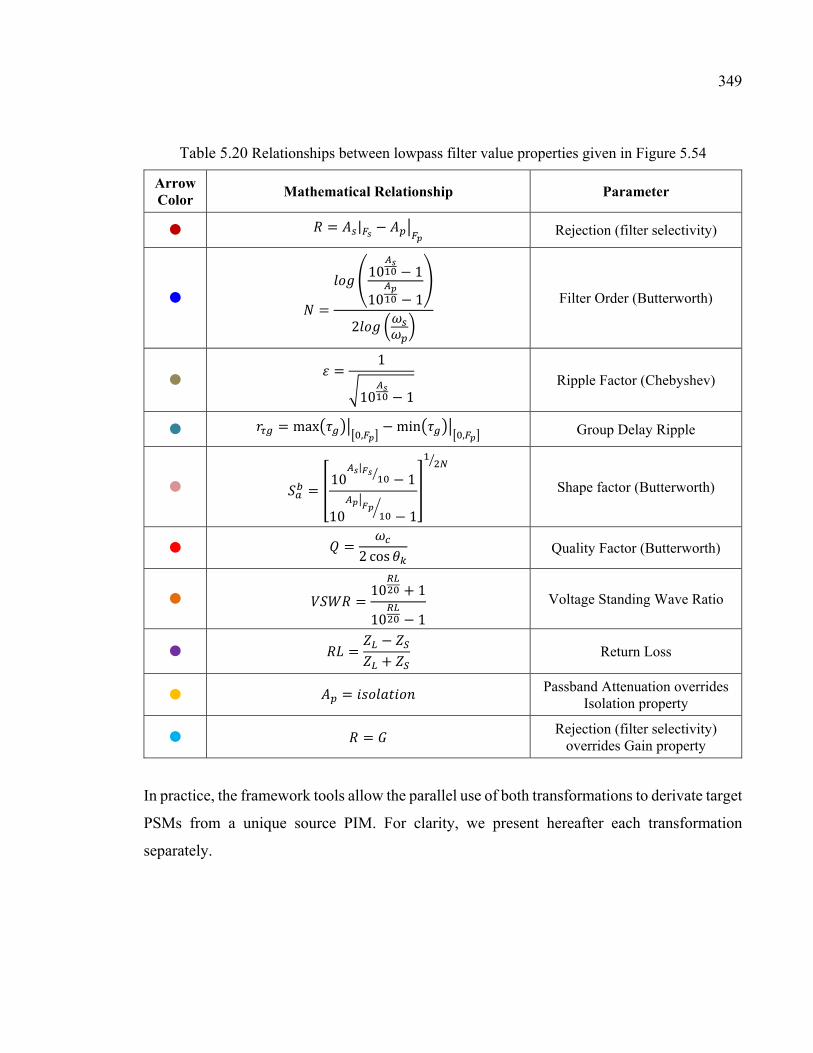
349
Table 5.20 Relationships between lowpass filter value properties given in Figure 5.54
Arrow Color
Mathematical Relationship Parameter
= | − Rejection (filter selectivity)
= 10 − 110 − 12 Filter Order (Butterworth)
= 110 − 1
Ripple Factor (Chebyshev)
= max , − min , Group Delay Ripple
= 10 | − 110 − 1 Shape factor (Butterworth)
= 2 cos Quality Factor (Butterworth)
= 10 + 110 − 1 Voltage Standing Wave Ratio
= −+ Return Loss
= Passband Attenuation overrides Isolation property
= Rejection (filter selectivity)
overrides Gain property
In practice, the framework tools allow the parallel use of both transformations to derivate target
PSMs from a unique source PIM. For clarity, we present hereafter each transformation
separately.
350
Figure 5.55 Lowpass filter coherence verification report
a) Stepped-impedance lines transformation
• Analysis: PSM generation The first transformation composed of three steps derives distributed-line sections to
approximate capacitive and inductive components.
1. Step 1: Determination of high and low characteristic impedances depending on target
distributed lines
The low and high characteristic impedances for capacitive and inductive line sections are
chosen at this step with respect to the following considerations (already enumerated in Hong
et Lancaster, 2001, p. 113):
− System reference impedance: The reference impedance (commonly = 50Ω) is higher
(respectively lower) than the low (respectively high) characteristic impedance (i.e., << ).
− Feasible dimensions of capacitive sections: The lowest is, the better the lumped-
element capacitor approximation is. The lowest is, the largest the corresponding line
width is. However, is limited by causing transverse resonance to occur at
operation frequencies.
− Feasible dimensions of inductive sections: The highest is, the better the lumped-
element inductor approximation is. The highest is, the thinnest the corresponding
line width is. The practical implementation of the line section becomes dependent on
the smallest feasible line width .
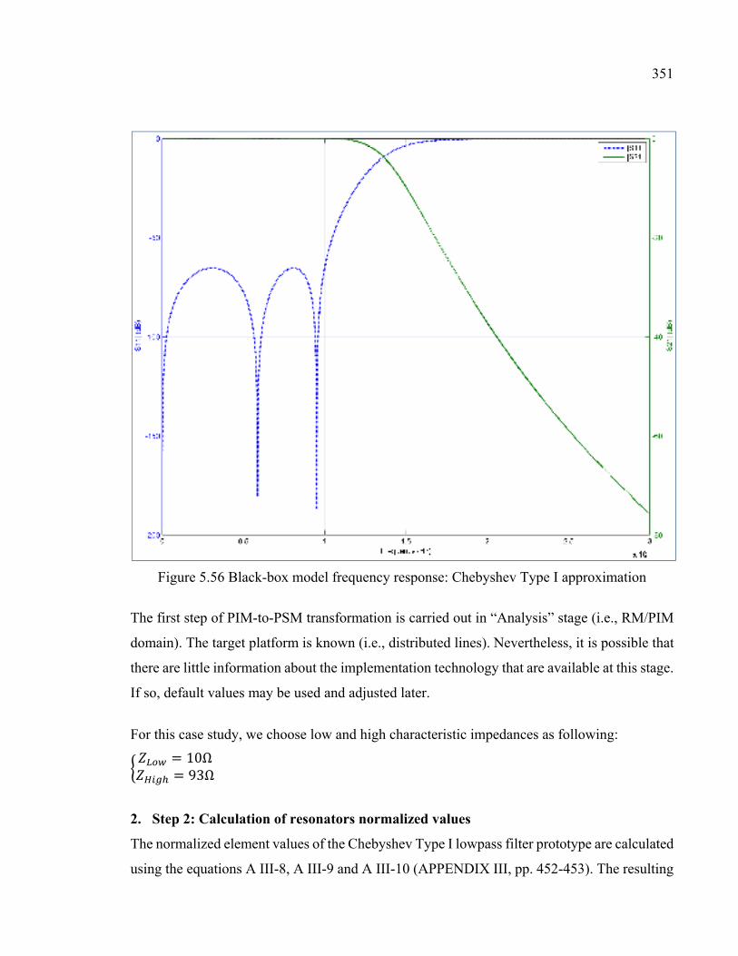
351
Figure 5.56 Black-box model frequency response: Chebyshev Type I approximation
The first step of PIM-to-PSM transformation is carried out in “Analysis” stage (i.e., RM/PIM
domain). The target platform is known (i.e., distributed lines). Nevertheless, it is possible that
there are little information about the implementation technology that are available at this stage.
If so, default values may be used and adjusted later.
For this case study, we choose low and high characteristic impedances as following: = 10Ω= 93Ω
2. Step 2: Calculation of resonators normalized values
The normalized element values of the Chebyshev Type I lowpass filter prototype are calculated
using the equations A III-8, A III-9 and A III-10 (APPENDIX III, pp. 452-453). The resulting
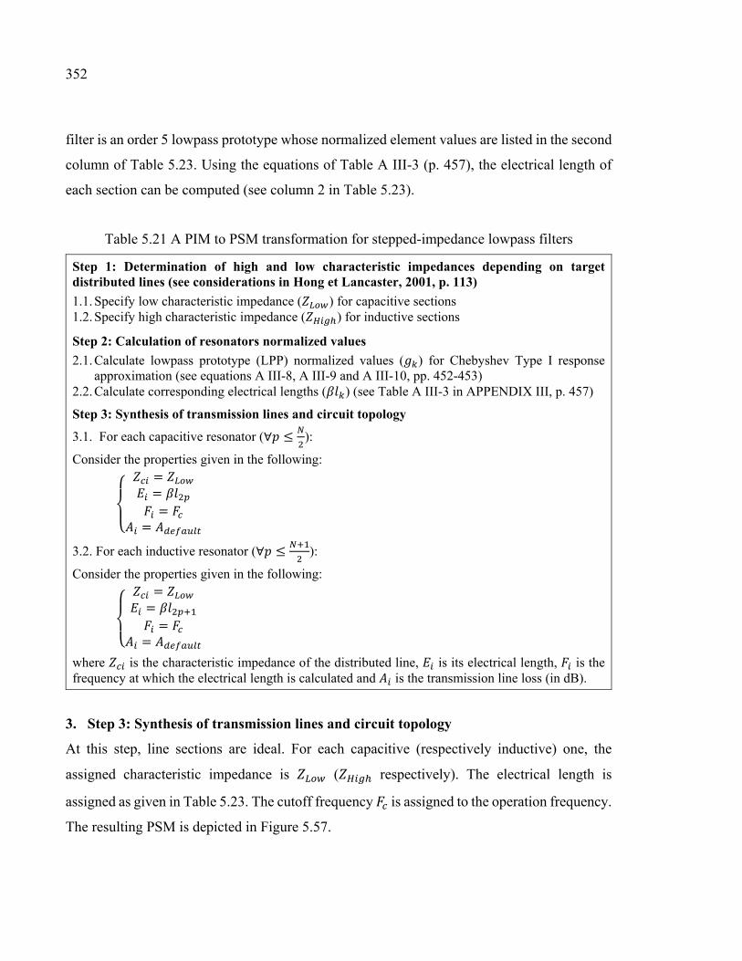
352
filter is an order 5 lowpass prototype whose normalized element values are listed in the second
column of Table 5.23. Using the equations of Table A III-3 (p. 457), the electrical length of
each section can be computed (see column 2 in Table 5.23).
Table 5.21 A PIM to PSM transformation for stepped-impedance lowpass filters
Step 1: Determination of high and low characteristic impedances depending on target distributed lines (see considerations in Hong et Lancaster, 2001, p. 113)
1.1. Specify low characteristic impedance ( ) for capacitive sections 1.2. Specify high characteristic impedance ( ) for inductive sections
Step 2: Calculation of resonators normalized values
2.1. Calculate lowpass prototype (LPP) normalized values ( ) for Chebyshev Type I response approximation (see equations A III-8, A III-9 and A III-10, pp. 452-453)
2.2. Calculate corresponding electrical lengths ( ) (see Table A III-3 in APPENDIX III, p. 457)
Step 3: Synthesis of transmission lines and circuit topology
3.1. For each capacitive resonator (∀ ≤ ):
Consider the properties given in the following: ====
3.2. For each inductive resonator (∀ ≤ ):
Consider the properties given in the following: ====
where is the characteristic impedance of the distributed line, is its electrical length, is the frequency at which the electrical length is calculated and is the transmission line loss (in dB).
3. Step 3: Synthesis of transmission lines and circuit topology
At this step, line sections are ideal. For each capacitive (respectively inductive) one, the
assigned characteristic impedance is ( respectively). The electrical length is
assigned as given in Table 5.23. The cutoff frequency is assigned to the operation frequency.
The resulting PSM is depicted in Figure 5.57.
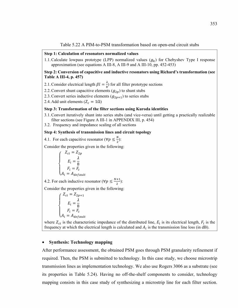
353
Table 5.22 A PIM-to-PSM transformation based on open-end circuit stubs
Step 1: Calculation of resonators normalized values
1.1. Calculate lowpass prototype (LPP) normalized values ( ) for Chebyshev Type I response approximation (see equations A III-8, A III-9 and A III-10, pp. 452-453)
Step 2: Conversion of capacitive and inductive resonators using Richard’s transformation (see Table A III-4, p. 457)
2.1. Consider electrical length = ) for all filter prototype sections
2.2. Convert shunt capacitive elements ( ) to shunt stubs 2.3. Convert series inductive elements ( ) to series stubs 2.4. Add unit elements ( = 1Ω)
Step 3: Transformation of the filter sections using Kuroda identities
3.1. Convert iteratively shunt into series stubs (and vice-versa) until getting a practically realizable filter sections (see Figure A III-1 in APPENDIX III, p. 454)
3.2. Frequency and impedance scaling of all sections
Step 4: Synthesis of transmission lines and circuit topology
4.1. For each capacitive resonator (∀ ≤ ):
Consider the properties given in the following: == 8==
4.2. For each inductive resonator (∀ ≤ ):
Consider the properties given in the following: == 8==
where is the characteristic impedance of the distributed line, is its electrical length, is the frequency at which the electrical length is calculated and is the transmission line loss (in dB).
• Synthesis: Technology mapping
After performance assessment, the obtained PSM goes through PSM granularity refinement if
required. Then, the PSM is submitted to technology. In this case study, we choose microstrip
transmission lines as implementation technology. We also use Rogers 3006 as a substrate (see
its properties in Table 5.24). Having no off-the-shelf components to consider, technology
mapping consists in this case study of synthesizing a microstrip line for each filter section.
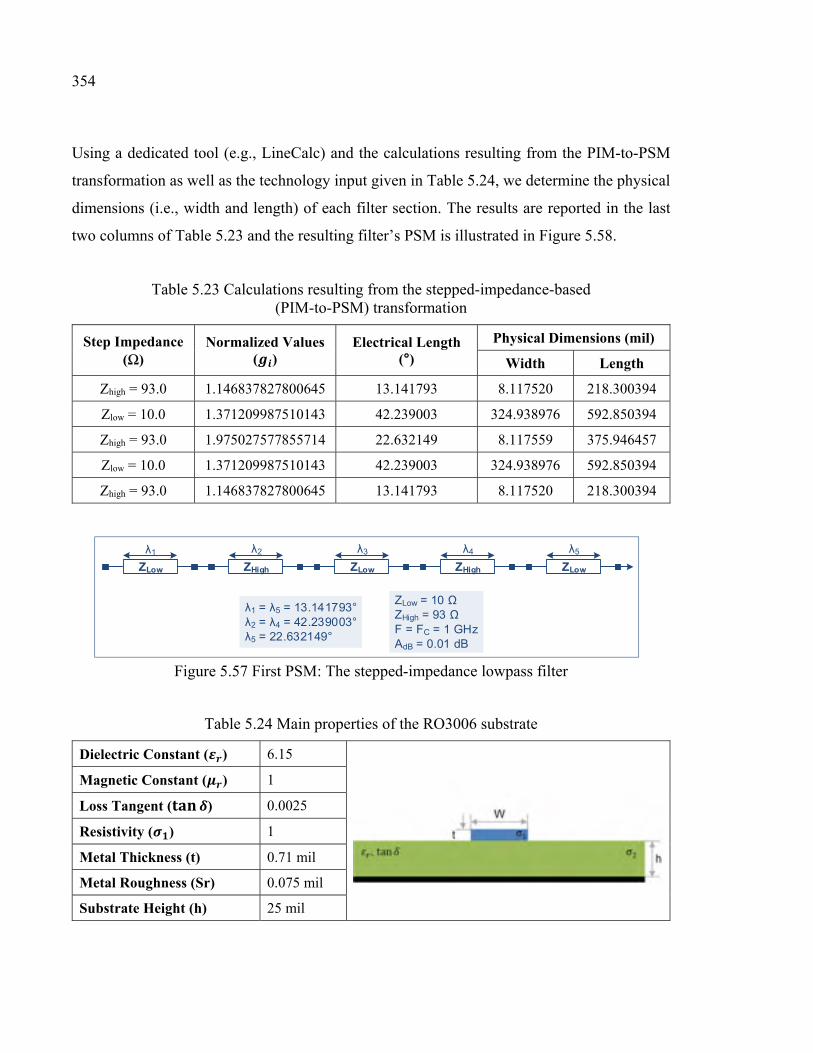
354
Using a dedicated tool (e.g., LineCalc) and the calculations resulting from the PIM-to-PSM
transformation as well as the technology input given in Table 5.24, we determine the physical
dimensions (i.e., width and length) of each filter section. The results are reported in the last
two columns of Table 5.23 and the resulting filter’s PSM is illustrated in Figure 5.58.
Table 5.23 Calculations resulting from the stepped-impedance-based (PIM-to-PSM) transformation
Step Impedance (Ω)
Normalized Values ( )
Electrical Length (°)
Physical Dimensions (mil)
Width Length
Zhigh = 93.0 1.146837827800645 13.141793 8.117520 218.300394
Zlow = 10.0 1.371209987510143 42.239003 324.938976 592.850394
Zhigh = 93.0 1.975027577855714 22.632149 8.117559 375.946457
Zlow = 10.0 1.371209987510143 42.239003 324.938976 592.850394
Zhigh = 93.0 1.146837827800645 13.141793 8.117520 218.300394
ZHighZLow ZLow ZHigh ZLow
λ1 λ2 λ3 λ4 λ5
λ1 = λ5 = 13.141793° λ2 = λ4 = 42.239003°λ5 = 22.632149°
ZLow = 10 Ω ZHigh = 93 ΩF = FC = 1 GHzAdB = 0.01 dB
Figure 5.57 First PSM: The stepped-impedance lowpass filter
Table 5.24 Main properties of the RO3006 substrate
Dielectric Constant ( ) 6.15
Magnetic Constant ( ) 1
Loss Tangent ( ) 0.0025
Resistivity ( ) 1
Metal Thickness (t) 0.71 mil
Metal Roughness (Sr) 0.075 mil
Substrate Height (h) 25 mil
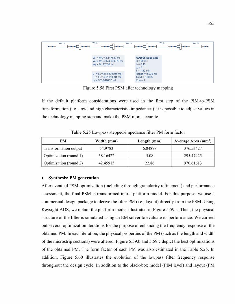
355
W1, L1
W1 = W5 = 8.117520 mil W2 = W4 = 324.938976 milW5 = 8.117559 mil
W2, L2 W3, L3 W4, L4 W5, L5
L1 = L5 = 218.300394 mil L2 = L4 = 592.850394 milL5 = 375.946457 mil
RO3006 SubstrateH = 25 milεr = 6.15 μr = 1 T = 1.42 milRough = 0.095 milTand = 0.0025Rho = 1
Figure 5.58 First PSM after technology mapping
If the default platform considerations were used in the first step of the PIM-to-PSM
transformation (i.e., low and high characteristic impedances), it is possible to adjust values in
the technology mapping step and make the PSM more accurate.
Table 5.25 Lowpass stepped-impedance filter PM form factor
PM Width (mm) Length (mm) Average Area (mm2)
Transformation output 54.9783 6.84878 376.53427
Optimization (round 1) 58.16422 5.08 295.47425
Optimization (round 2) 42.45915 22.86 970.61613
• Synthesis: PM generation
After eventual PSM optimization (including through granularity refinement) and performance
assessment, the final PSM is transformed into a platform model. For this purpose, we use a
commercial design package to derive the filter PM (i.e., layout) directly from the PSM. Using
Keysight ADS, we obtain the platform model illustrated in Figure 5.59.a. Then, the physical
structure of the filter is simulated using an EM solver to evaluate its performance. We carried
out several optimization iterations for the purpose of enhancing the frequency response of the
obtained PM. In each iteration, the physical properties of the PM (such as the length and width
of the microstrip sections) were altered. Figure 5.59.b and 5.59.c depict the best optimizations
of the obtained PM. The form factor of each PM was also estimated in the Table 5.25. In
addition, Figure 5.60 illustrates the evolution of the lowpass filter frequency response
throughout the design cycle. In addition to the black-box model (PIM level) and layout (PM
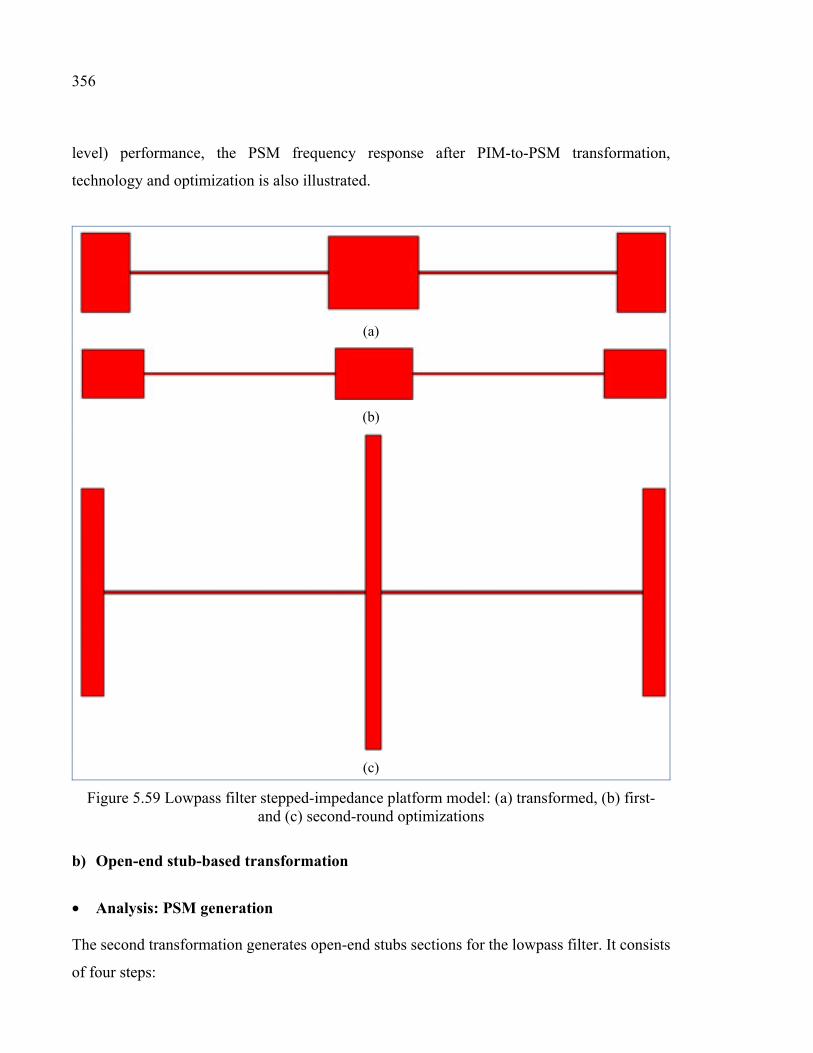
356
level) performance, the PSM frequency response after PIM-to-PSM transformation,
technology and optimization is also illustrated.
(a)
(b)
(c)
Figure 5.59 Lowpass filter stepped-impedance platform model: (a) transformed, (b) first- and (c) second-round optimizations
b) Open-end stub-based transformation
• Analysis: PSM generation The second transformation generates open-end stubs sections for the lowpass filter. It consists
of four steps:
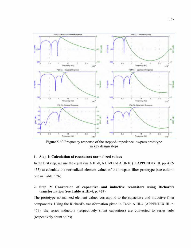
357
Figure 5.60 Frequency response of the stepped-impedance lowpass prototype in key design steps
1. Step 1: Calculation of resonators normalized values
In the first step, we use the equations A III-8, A III-9 and A III-10 (in APPENDIX III, pp. 452-
453) to calculate the normalized element values of the lowpass filter prototype (see column
one in Table 5.26).
2. Step 2: Conversion of capacitive and inductive resonators using Richard’s
transformation (see Table A III-4, p. 457)
The prototype normalized element values correspond to the capacitive and inductive filter
components. Using the Richard’s transformation given in Table A III-4 (APPENDIX III, p.
457), the series inductors (respectively shunt capacitors) are converted to series subs
(respectively shunt stubs).
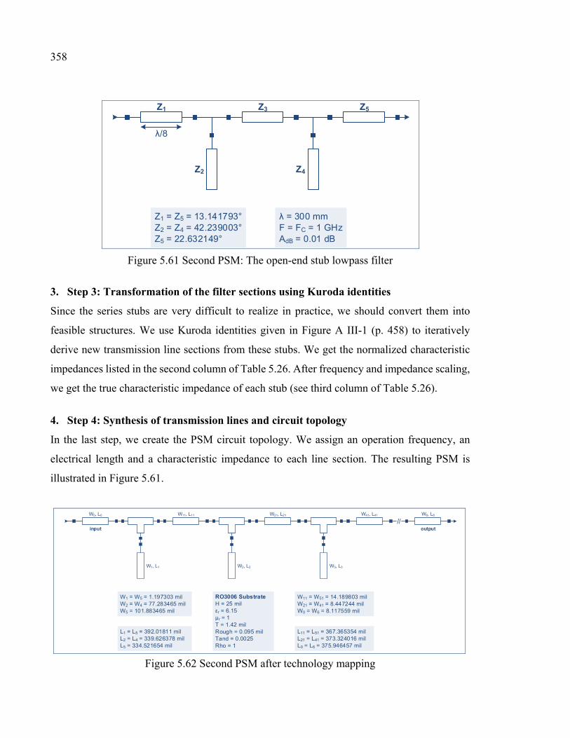
358
Z1 Z3
Z2
Z5
Z4
Z1 = Z5 = 13.141793° Z2 = Z4 = 42.239003°Z5 = 22.632149°
λ = 300 mm F = FC = 1 GHzAdB = 0.01 dB
λ/8
Figure 5.61 Second PSM: The open-end stub lowpass filter
3. Step 3: Transformation of the filter sections using Kuroda identities
Since the series stubs are very difficult to realize in practice, we should convert them into
feasible structures. We use Kuroda identities given in Figure A III-1 (p. 458) to iteratively
derive new transmission line sections from these stubs. We get the normalized characteristic
impedances listed in the second column of Table 5.26. After frequency and impedance scaling,
we get the true characteristic impedance of each stub (see third column of Table 5.26).
4. Step 4: Synthesis of transmission lines and circuit topology
In the last step, we create the PSM circuit topology. We assign an operation frequency, an
electrical length and a characteristic impedance to each line section. The resulting PSM is
illustrated in Figure 5.61.
//W0, L0 W11, L11 W21, L21 W41, L41 W6, L6
W1, L1 W2, L2 W3, L3
W1 = W5 = 1.197303 mil W2 = W4 = 77.283465 milW5 = 101.883465 mil
L1 = L5 = 392.01811 mil L2 = L4 = 339.626378 milL5 = 334.521654 mil
RO3006 SubstrateH = 25 milεr = 6.15 μr = 1 T = 1.42 milRough = 0.095 milTand = 0.0025Rho = 1
W11 = W51 = 14.189803 mil W21 = W41 = 8.447244 milW0 = W6 = 8.117559 mil
L11 = L51 = 367.365354 mil L21 = L41 = 373.324016 milL0 = L6 = 375.946457 mil
input output
Figure 5.62 Second PSM after technology mapping
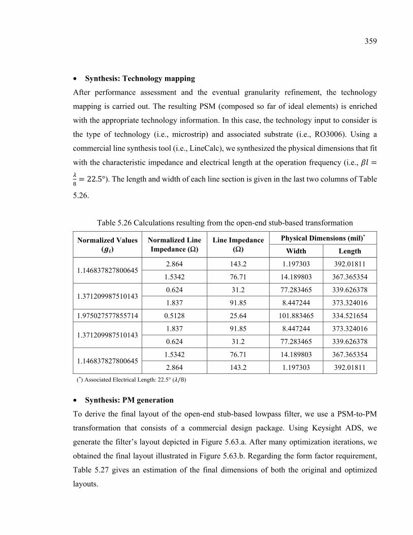
359
• Synthesis: Technology mapping
After performance assessment and the eventual granularity refinement, the technology
mapping is carried out. The resulting PSM (composed so far of ideal elements) is enriched
with the appropriate technology information. In this case, the technology input to consider is
the type of technology (i.e., microstrip) and associated substrate (i.e., RO3006). Using a
commercial line synthesis tool (i.e., LineCalc), we synthesized the physical dimensions that fit
with the characteristic impedance and electrical length at the operation frequency (i.e., == 22.5°). The length and width of each line section is given in the last two columns of Table
5.26.
Table 5.26 Calculations resulting from the open-end stub-based transformation
Normalized Values ( )
Normalized Line Impedance (Ω)
Line Impedance (Ω)
Physical Dimensions (mil)*
Width Length
1.146837827800645 2.864 143.2 1.197303 392.01811
1.5342 76.71 14.189803 367.365354
1.371209987510143 0.624 31.2 77.283465 339.626378
1.837 91.85 8.447244 373.324016
1.975027577855714 0.5128 25.64 101.883465 334.521654
1.371209987510143 1.837 91.85 8.447244 373.324016
0.624 31.2 77.283465 339.626378
1.146837827800645 1.5342 76.71 14.189803 367.365354
2.864 143.2 1.197303 392.01811
(*) Associated Electrical Length: 22.5° ( /8)
• Synthesis: PM generation
To derive the final layout of the open-end stub-based lowpass filter, we use a PSM-to-PM
transformation that consists of a commercial design package. Using Keysight ADS, we
generate the filter’s layout depicted in Figure 5.63.a. After many optimization iterations, we
obtained the final layout illustrated in Figure 5.63.b. Regarding the form factor requirement,
Table 5.27 gives an estimation of the final dimensions of both the original and optimized
layouts.
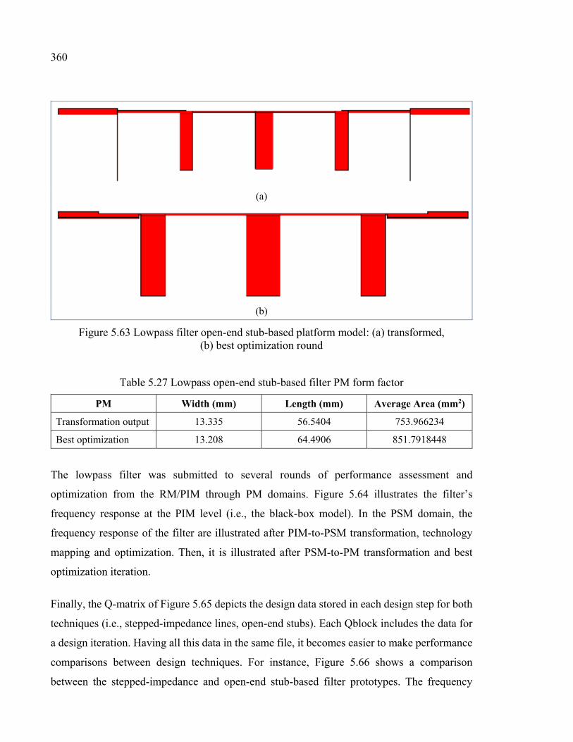
360
(a)
(b)
Figure 5.63 Lowpass filter open-end stub-based platform model: (a) transformed, (b) best optimization round
Table 5.27 Lowpass open-end stub-based filter PM form factor
PM Width (mm) Length (mm) Average Area (mm2)
Transformation output 13.335 56.5404 753.966234
Best optimization 13.208 64.4906 851.7918448
The lowpass filter was submitted to several rounds of performance assessment and
optimization from the RM/PIM through PM domains. Figure 5.64 illustrates the filter’s
frequency response at the PIM level (i.e., the black-box model). In the PSM domain, the
frequency response of the filter are illustrated after PIM-to-PSM transformation, technology
mapping and optimization. Then, it is illustrated after PSM-to-PM transformation and best
optimization iteration.
Finally, the Q-matrix of Figure 5.65 depicts the design data stored in each design step for both
techniques (i.e., stepped-impedance lines, open-end stubs). Each Qblock includes the data for
a design iteration. Having all this data in the same file, it becomes easier to make performance
comparisons between design techniques. For instance, Figure 5.66 shows a comparison
between the stepped-impedance and open-end stub-based filter prototypes. The frequency

361
response (particularly within the transition band) of the latter is better than the former. This
result is expected because the coarse approximations involved in the stepped-impedance filter
degrade the overall performance (Pozar, 2012, p. 470).
Figure 5.64 Frequency response of the open-end stubs lowpass prototype in key design steps
5.3.2 Power Attenuation Device
In this case study, we attempt to use the proposed framework for concurrent design. We
undertake the design of a power attenuation device, an attenuator. We develop in parallel two
prototypes that are optimized, validated and compared throughout the design cycle.
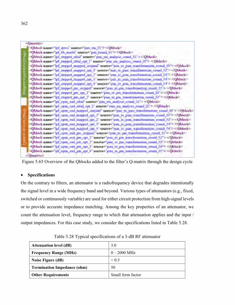
362
Figure 5.65 Overview of the Qblocks added to the filter’s Q-matrix through the design cycle
• Specifications
On the contrary to filters, an attenuator is a radiofrequency device that degrades intentionally
the signal level in a wide frequency band and beyond. Various types of attenuators (e.g., fixed,
switched or continuously variable) are used for either circuit protection from high-signal levels
or to provide accurate impedance matching. Among the key properties of an attenuator, we
count the attenuation level, frequency range to which that attenuation applies and the input /
output impedances. For this case study, we consider the specifications listed in Table 5.28.
Table 5.28 Typical specifications of a 3-dB RF attenuator
Attenuation level (dB) 3.0
Frequency Range (MHz) 0 – 2000 MHz
Noise Figure (dB) < 0.5
Termination Impedance (ohm) 50
Other Requirements Small form factor
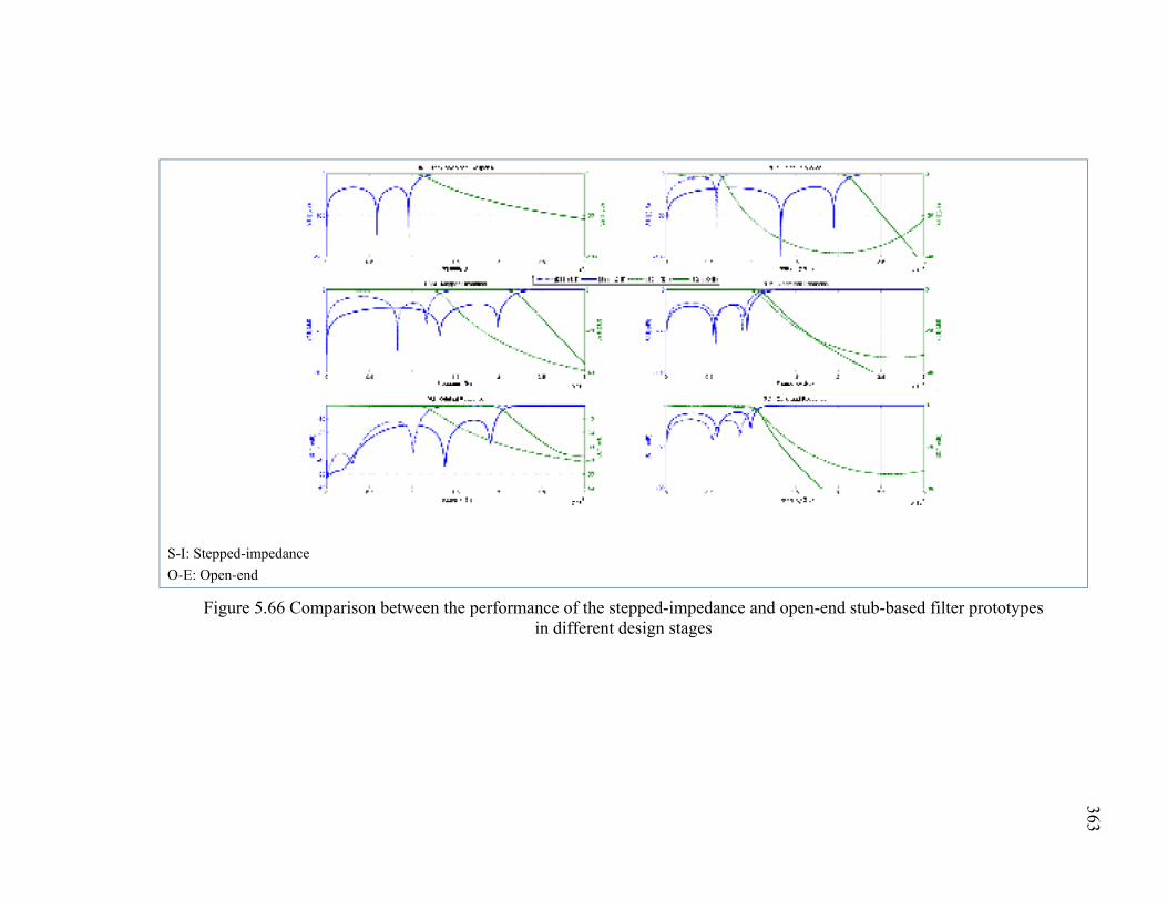
S-I: Stepped-impedance
O-E: Open-end
Figure 5.66 Comparison between the performance of the stepped-impedance and open-end stub-based filter prototypes in different design stages
363
364
• Functional Description: SysML requirements and platform-independent models
The SysML diagrams used for the attenuator’s functional description are similar to those
elaborated for bandpass and lowpass filters. The package diagram of Figure 5.67 depicts the
main constituents of the functional description:
− Attenuator definition: this package defines the functional and structural aspects of the
attenuator. Its general organization is inspired from the RF stereotypes bdd illustrated in
Figure 4.50. For example, the bdd of Figure 5.68 shows the properties of the attenuator
block as well as the hierarchy of blocks related to it. Thus, an attenuator inherits the
properties of the « Power Attenuation and Matching Device », which is itself a linear two-
port network. The complete list of attenuator values are given in Table 5.29. The values of
« Port » block are provided separately in Table 5.30;
− Attenuator requirements: as shown in Figure 5.69, the requirements related to the
attenuator design are similar to those depicted in Figure 4.55. In this case, the attenuator
requirements can be subdivided into two major categories: performance and form factor.
The first includes the required attenuation level and its associated frequency range. The
second summarizes the requirements related to the form and size of the device;
− Attenuator coherence rules: the functional description of the attenuator is submitted in the
next design stage, namely « Analysis ». The related rules are assembled in « Coherence
Rules » package (see Figure 5.67) that is detailed in the next design stage;
− Value types: this package defines the units, constants and other modeling artifacts used in
the other packages. As illustrated in Figure 5.70, the units used in attenuator definition bdds
to define values’ types are reported.
It is worth noting that the SysML diagrams shown in this section are part of the attenuator
functional description but not exhaustive and presented for illustration purposes only.
• Analysis: Coherence verification
The attenuator’s functional description should be submitted to coherence verification at this
step in order to figure out any eventual errors. The set of rules used for this process is composed
of electrical consistence and integrity controls rules. No PIM-level design constraints’ rules
are defined for this case study.
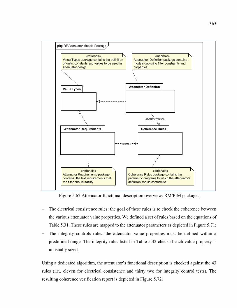
365
Value Types
pkg RF Attenuator Models Package
«rationale»Attenuator Definition package contains models capturing filter constraints and properties
Attenuator Definition
Attenuator Requirements
«rationale»Attenuator Requirements package contains the text requirements that the filter should satisfy
«rationale»Value Types package contains the definition of units, constants and values to be used in attenuator design
«rationale»Coherence Rules package contains the parametric diagrams to which the attenuator’s definition should conform to
Coherence Rules
«conforms to»
«uses»
Figure 5.67 Attenuator functional description overview: RM/PIM packages
− The electrical consistence rules: the goal of these rules is to check the coherence between
the various attenuator value properties. We defined a set of rules based on the equations of
Table 5.31. These rules are mapped to the attenuator parameters as depicted in Figure 5.71;
− The integrity controls rules: the attenuator value properties must be defined within a
predefined range. The integrity rules listed in Table 5.32 check if each value property is
unusually sized.
Using a dedicated algorithm, the attenuator’s functional description is checked against the 43
rules (i.e., eleven for electrical consistence and thirty two for integrity control tests). The
resulting coherence verification report is depicted in Figure 5.72.
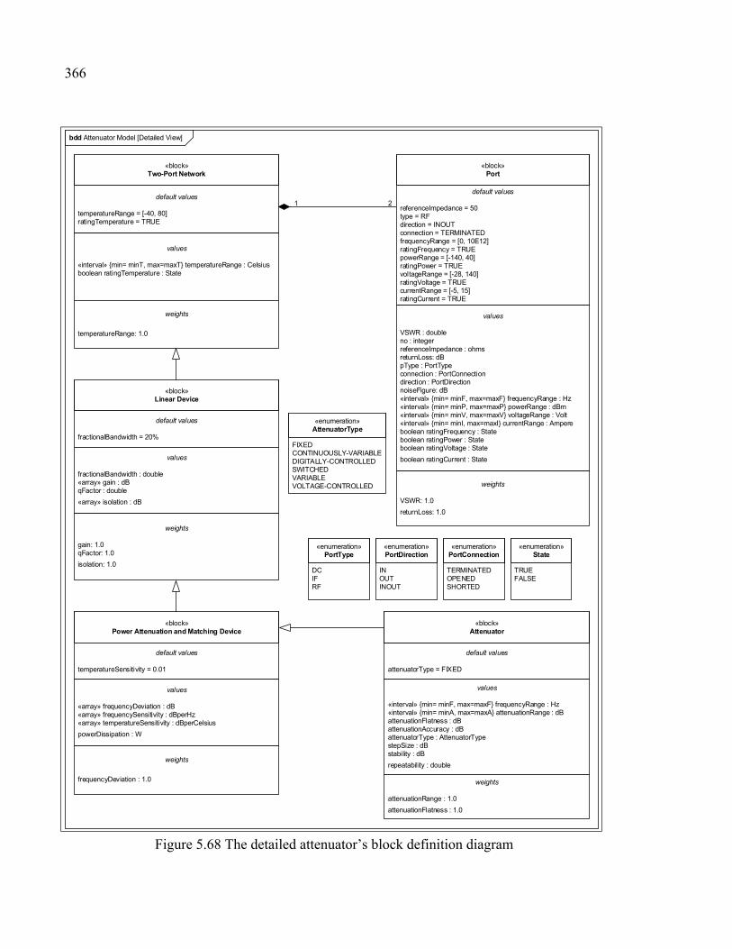
366
bdd Attenuator Model [Detailed View]
«block»Two-Port Network
default values
temperatureRange = [-40, 80]ratingTemperature = TRUE
«block»Port
values
«interval» min= minT, max=maxT temperatureRange : Celsiusboolean ratingTemperature : State
weights
temperatureRange: 1.0
1 2
default values
referenceImpedance = 50type = RFdirection = INOUTconnection = TERMINATEDfrequencyRange = [0, 10E12]ratingFrequency = TRUEpowerRange = [-140, 40]ratingPower = TRUEvoltageRange = [-28, 140]ratingVoltage = TRUEcurrentRange = [-5, 15]ratingCurrent = TRUE
values
VSWR : doubleno : integerreferenceImpedance : ohmsreturnLoss: dBpType : PortTypeconnection : PortConnectiondirection : PortDirectionnoiseFigure: dB«interval» min= minF, max=maxF frequencyRange : Hz«interval» min= minP, max=maxP powerRange : dBm«interval» min= minV, max=maxV voltageRange : Volt«interval» min= minI, max=maxI currentRange : Ampereboolean ratingFrequency : Stateboolean ratingPower : Stateboolean ratingVoltage : State
boolean ratingCurrent : State
weights
VSWR: 1.0
returnLoss: 1.0
«block»Linear Device
default values
fractionalBandwidth = 20%
values
fractionalBandwidth : double«array» gain : dBqFactor : double
«array» isolation : dB
weights
gain: 1.0qFactor: 1.0
isolation: 1.0
«enumeration»PortConnection
TERMINATEDOPENEDSHORTED
«enumeration»State
TRUEFALSE
«enumeration»PortType
DCIFRF
«enumeration»PortDirection
INOUTINOUT
«block»Power Attenuation and Matching Device
default values
temperatureSensitivity = 0.01
values
«array» frequencyDeviation : dB«array» frequencySensitivity : dBperHz«array» temperatureSensitivity : dBperCelsius
powerDissipation : W
weights
frequencyDeviation : 1.0
default values
attenuatorType = FIXED
values
«interval» min= minF, max=maxF frequencyRange : Hz«interval» min= minA, max=maxA attenuationRange : dBattenuationFlatness : dBattenuationAccuracy : dBattenuatorType : AttenuatorTypestepSize : dBstability : dB
repeatability : double
weights
attenuationRange : 1.0
attenuationFlatness : 1.0
«block»Attenuator
«enumeration»AttenuatorType
FIXEDCONTINUOUSLY-VARIABLEDIGITALLY-CONTROLLEDSWITCHEDVARIABLEVOLTAGE-CONTROLLED
Figure 5.68 The detailed attenuator’s block definition diagram
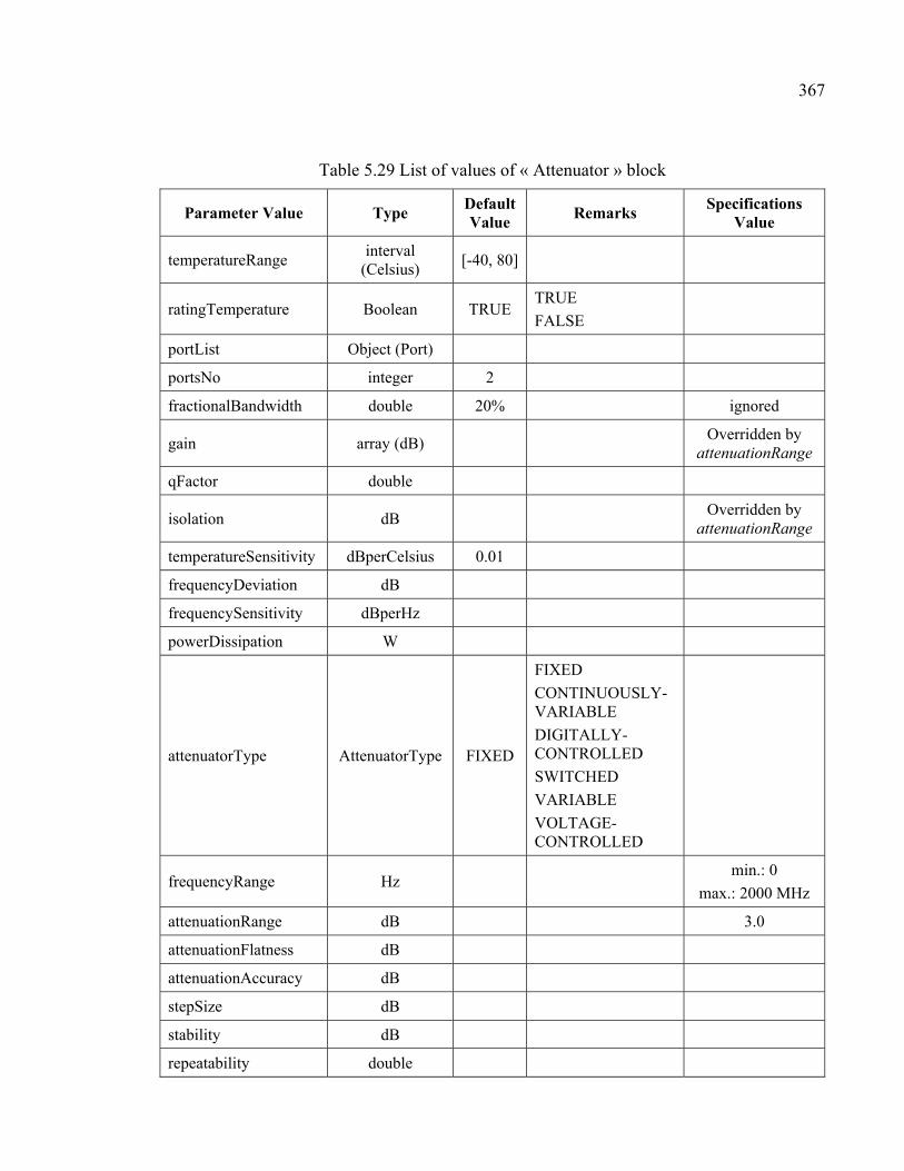
367
Table 5.29 List of values of « Attenuator » block
Parameter Value Type Default Value
Remarks Specifications
Value
temperatureRange interval
(Celsius) [-40, 80]
ratingTemperature Boolean TRUE TRUE
FALSE
portList Object (Port)
portsNo integer 2
fractionalBandwidth double 20% ignored
gain array (dB) Overridden by
attenuationRange
qFactor double
isolation dB Overridden by
attenuationRange
temperatureSensitivity dBperCelsius 0.01
frequencyDeviation dB
frequencySensitivity dBperHz
powerDissipation W
attenuatorType AttenuatorType FIXED
FIXED
CONTINUOUSLY-VARIABLE
DIGITALLY-CONTROLLED
SWITCHED
VARIABLE
VOLTAGE-CONTROLLED
frequencyRange Hz min.: 0
max.: 2000 MHz
attenuationRange dB 3.0
attenuationFlatness dB
attenuationAccuracy dB
stepSize dB
stability dB
repeatability double
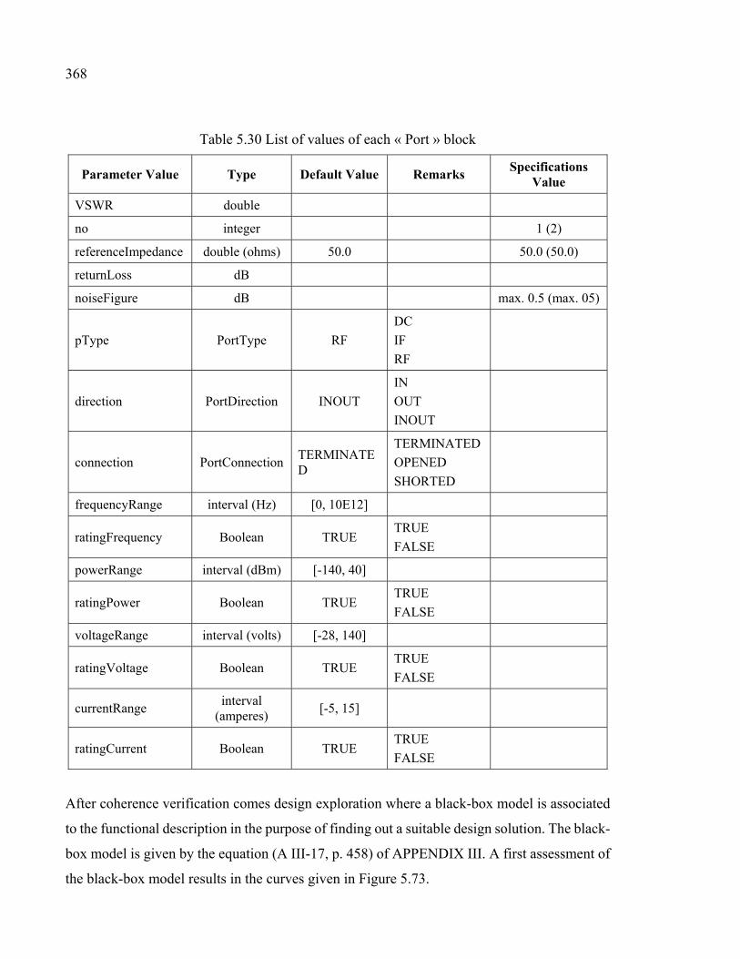
368
Table 5.30 List of values of each « Port » block
Parameter Value Type Default Value Remarks Specifications
Value
VSWR double
no integer 1 (2)
referenceImpedance double (ohms) 50.0 50.0 (50.0)
returnLoss dB
noiseFigure dB max. 0.5 (max. 05)
pType PortType RF
DC
IF
RF
direction PortDirection INOUT
IN
OUT
INOUT
connection PortConnection TERMINATED
TERMINATED
OPENED
SHORTED
frequencyRange interval (Hz) [0, 10E12]
ratingFrequency Boolean TRUE TRUE
FALSE
powerRange interval (dBm) [-140, 40]
ratingPower Boolean TRUE TRUE
FALSE
voltageRange interval (volts) [-28, 140]
ratingVoltage Boolean TRUE TRUE
FALSE
currentRange interval
(amperes) [-5, 15]
ratingCurrent Boolean TRUE TRUE
FALSE
After coherence verification comes design exploration where a black-box model is associated
to the functional description in the purpose of finding out a suitable design solution. The black-
box model is given by the equation (A III-17, p. 458) of APPENDIX III. A first assessment of
the black-box model results in the curves given in Figure 5.73.
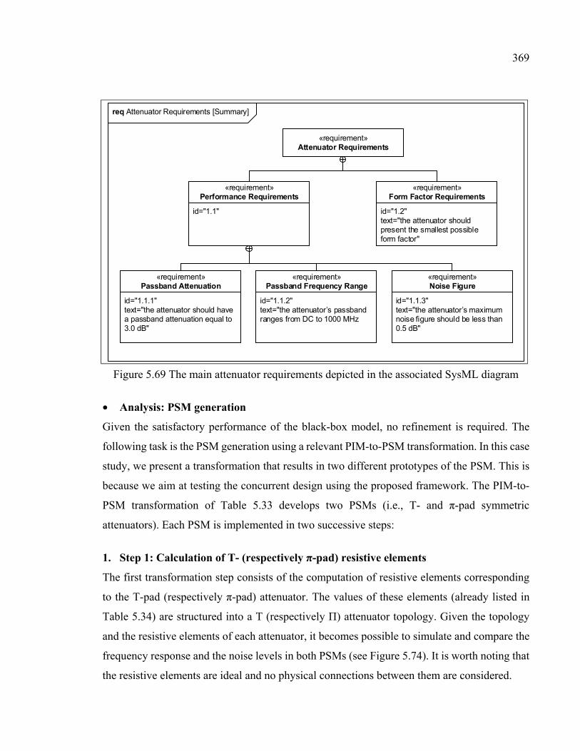
369
req Attenuator Requirements [Summary]
«requirement»Attenuator Requirements
id="1.2"text="the attenuator should present the smallest possible form factor"
«requirement»Form Factor Requirements
id="1.1.1"text="the attenuator should have a passband attenuation equal to 3.0 dB"
«requirement»Passband Attenuation
id="1.1.2"text="the attenuator’s passband ranges from DC to 1000 MHz
«requirement»Passband Frequency Range
id="1.1"
«requirement»Performance Requirements
id="1.1.3"text="the attenuator’s maximum noise figure should be less than 0.5 dB"
«requirement»Noise Figure
Figure 5.69 The main attenuator requirements depicted in the associated SysML diagram
• Analysis: PSM generation
Given the satisfactory performance of the black-box model, no refinement is required. The
following task is the PSM generation using a relevant PIM-to-PSM transformation. In this case
study, we present a transformation that results in two different prototypes of the PSM. This is
because we aim at testing the concurrent design using the proposed framework. The PIM-to-
PSM transformation of Table 5.33 develops two PSMs (i.e., T- and π-pad symmetric
attenuators). Each PSM is implemented in two successive steps:
1. Step 1: Calculation of T- (respectively π-pad) resistive elements
The first transformation step consists of the computation of resistive elements corresponding
to the T-pad (respectively π-pad) attenuator. The values of these elements (already listed in
Table 5.34) are structured into a T (respectively Π) attenuator topology. Given the topology
and the resistive elements of each attenuator, it becomes possible to simulate and compare the
frequency response and the noise levels in both PSMs (see Figure 5.74). It is worth noting that
the resistive elements are ideal and no physical connections between them are considered.
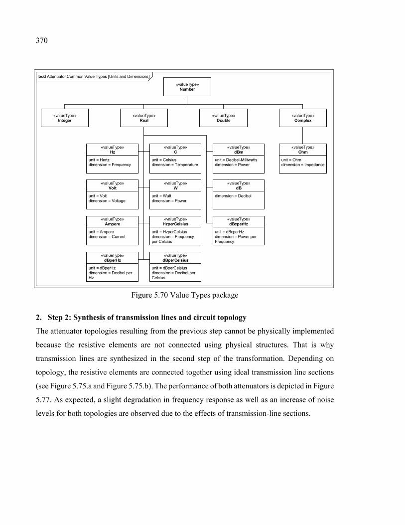
370
bdd Attenuator Common Value Types [Units and Dimensions]
«valueType»Complex
unit = Ohmdimension = Impedance
«valueType»Ohm
«valueType»Integer
«valueType»Double
«valueType»Number
«valueType»Real
unit = Celsiusdimension = Temperature
«valueType»C
unit = Wattdimension = Power
«valueType»W
unit = HzperCelsiusdimension = Frequency per Celcius
«valueType»HzperCelsius
unit = Voltdimension = Voltage
«valueType»Volt
unit = Hertzdimension = Frequency
«valueType»Hz
unit = Amperedimension = Current
«valueType»Ampere
unit = Decibel-Milliwattsdimension = Power
«valueType»dBm
dimension = Decibel
«valueType»dB
unit = dBcperHzdimension = Power per Frequency
«valueType»dBcperHz
unit = dBperCelsiusdimension = Decibel per Celcius
«valueType»dBperCelsius
unit = dBperHzdimension = Decibel per Hz
«valueType»dBperHz
Figure 5.70 Value Types package
2. Step 2: Synthesis of transmission lines and circuit topology
The attenuator topologies resulting from the previous step cannot be physically implemented
because the resistive elements are not connected using physical structures. That is why
transmission lines are synthesized in the second step of the transformation. Depending on
topology, the resistive elements are connected together using ideal transmission line sections
(see Figure 5.75.a and Figure 5.75.b). The performance of both attenuators is depicted in Figure
5.77. As expected, a slight degradation in frequency response as well as an increase of noise
levels for both topologies are observed due to the effects of transmission-line sections.
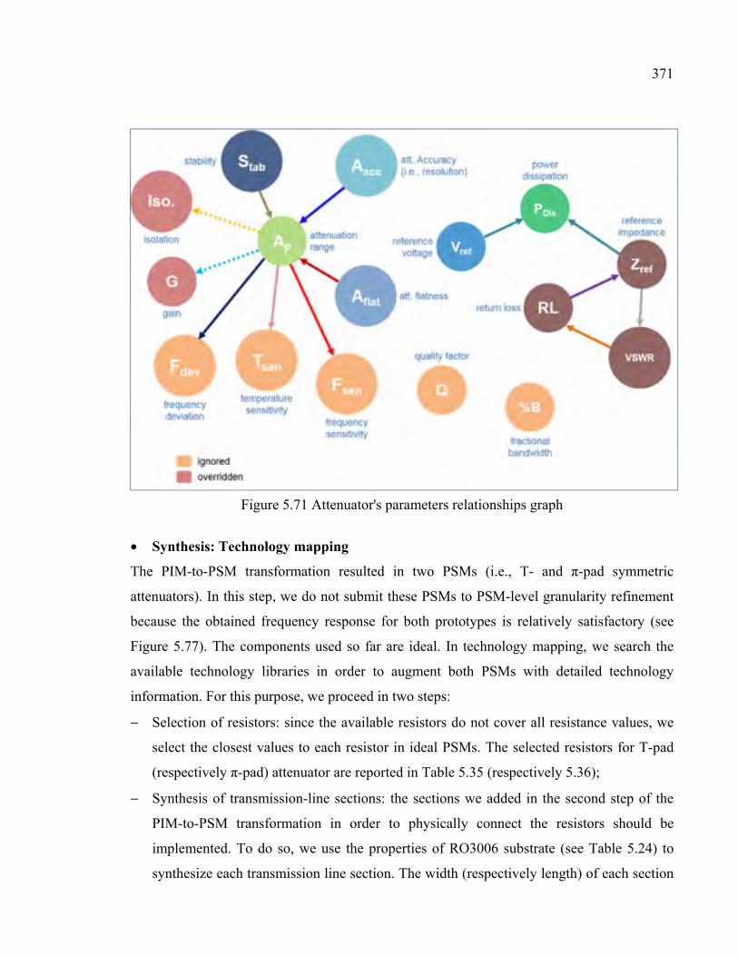
371
Figure 5.71 Attenuator's parameters relationships graph
• Synthesis: Technology mapping
The PIM-to-PSM transformation resulted in two PSMs (i.e., T- and π-pad symmetric
attenuators). In this step, we do not submit these PSMs to PSM-level granularity refinement
because the obtained frequency response for both prototypes is relatively satisfactory (see
Figure 5.77). The components used so far are ideal. In technology mapping, we search the
available technology libraries in order to augment both PSMs with detailed technology
information. For this purpose, we proceed in two steps:
− Selection of resistors: since the available resistors do not cover all resistance values, we
select the closest values to each resistor in ideal PSMs. The selected resistors for T-pad
(respectively π-pad) attenuator are reported in Table 5.35 (respectively 5.36);
− Synthesis of transmission-line sections: the sections we added in the second step of the
PIM-to-PSM transformation in order to physically connect the resistors should be
implemented. To do so, we use the properties of RO3006 substrate (see Table 5.24) to
synthesize each transmission line section. The width (respectively length) of each section
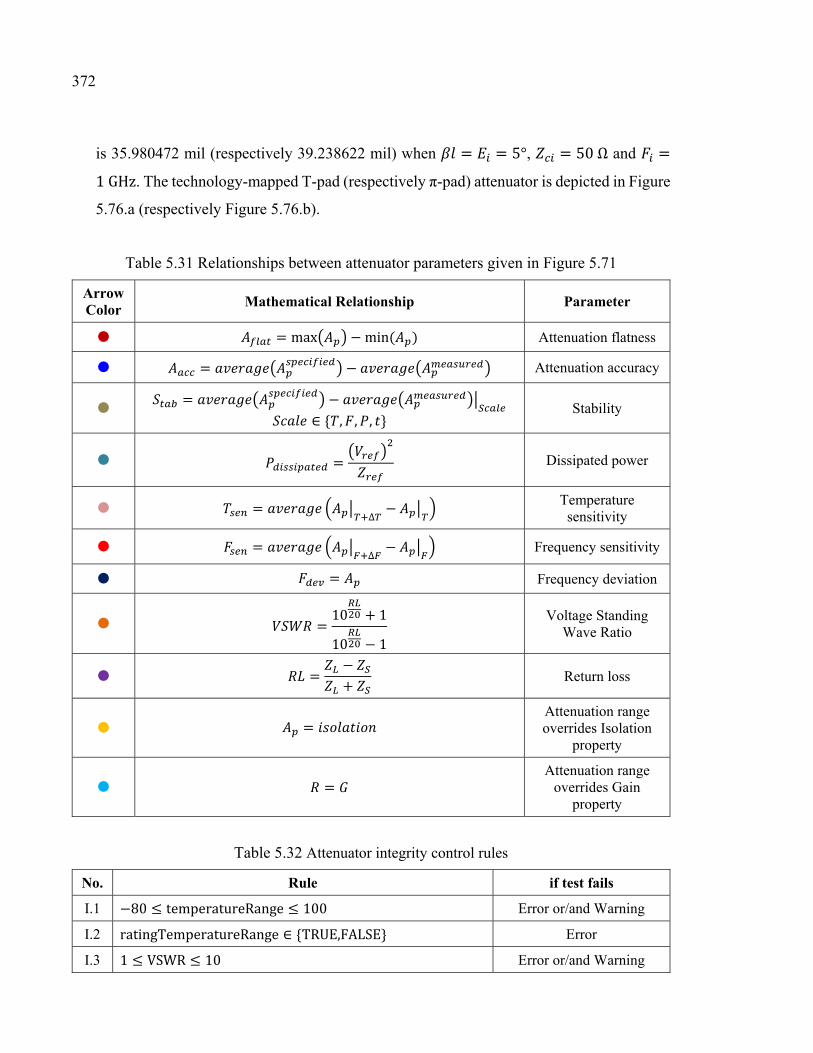
372
is 35.980472 mil (respectively 39.238622 mil) when = = 5°, = 50Ω and =1GHz. The technology-mapped T-pad (respectively π-pad) attenuator is depicted in Figure
5.76.a (respectively Figure 5.76.b).
Table 5.31 Relationships between attenuator parameters given in Figure 5.71
Arrow Color
Mathematical Relationship Parameter
= max − min( ) Attenuation flatness
= − Attenuation accuracy
= −∈ , , , Stability
= Dissipated power
= ∆ − Temperature sensitivity
= ∆ − Frequency sensitivity
= Frequency deviation
= 10 + 110 − 1 Voltage Standing
Wave Ratio
= −+ Return loss
= Attenuation range overrides Isolation
property
= Attenuation range
overrides Gain property
Table 5.32 Attenuator integrity control rules
No. Rule if test fails
I.1 −80 ≤ temperatureRange ≤ 100 Error or/and Warning
I.2 ratingTemperatureRange ∈ TRUE,FALSE Error
I.3 1 ≤ VSWR ≤ 10 Error or/and Warning
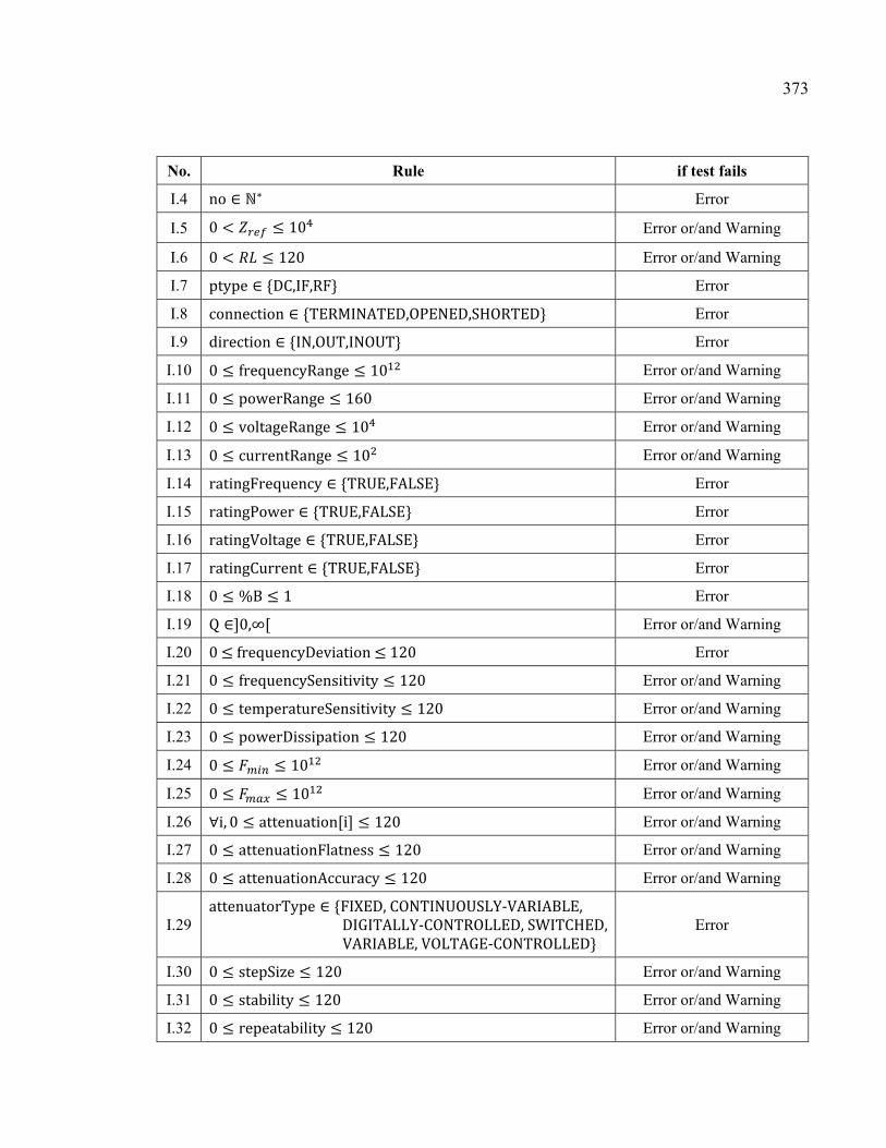
373
No. Rule if test fails
I.4 no ∈ ℕ∗ Error
I.5 0 < ≤ 10 Error or/and Warning
I.6 0 < ≤ 120 Error or/and Warning
I.7 ptype ∈ DC,IF,RF Error
I.8 connection ∈ TERMINATED,OPENED,SHORTED Error
I.9 direction ∈ IN,OUT,INOUT Error
I.10 0 ≤ frequencyRange ≤ 10 Error or/and Warning
I.11 0 ≤ powerRange ≤ 160 Error or/and Warning
I.12 0 ≤ voltageRange ≤ 10 Error or/and Warning
I.13 0 ≤ currentRange ≤ 10 Error or/and Warning
I.14 ratingFrequency ∈ TRUE,FALSE Error
I.15 ratingPower ∈ TRUE,FALSE Error
I.16 ratingVoltage ∈ TRUE,FALSE Error
I.17 ratingCurrent ∈ TRUE,FALSE Error
I.18 0 ≤ %B ≤ 1 Error
I.19 Q ∈]0,∞[ Error or/and Warning
I.20 0≤frequencyDeviation≤120 Error
I.21 0 ≤ frequencySensitivity ≤ 120 Error or/and Warning
I.22 0 ≤ temperatureSensitivity ≤ 120 Error or/and Warning
I.23 0 ≤ powerDissipation ≤ 120 Error or/and Warning
I.24 0 ≤ ≤ 10 Error or/and Warning
I.25 0 ≤ ≤ 10 Error or/and Warning
I.26 ∀i, 0 ≤ attenuation[i] ≤ 120 Error or/and Warning
I.27 0 ≤ attenuationFlatness ≤ 120 Error or/and Warning
I.28 0 ≤ attenuationAccuracy ≤ 120 Error or/and Warning
I.29 attenuatorType ∈ FIXED,CONTINUOUSLY-VARIABLE,DIGITALLY-CONTROLLED,SWITCHED,VARIABLE,VOLTAGE-CONTROLLED Error
I.30 0 ≤ stepSize ≤ 120 Error or/and Warning
I.31 0 ≤ stability ≤ 120 Error or/and Warning
I.32 0 ≤ repeatability ≤ 120 Error or/and Warning
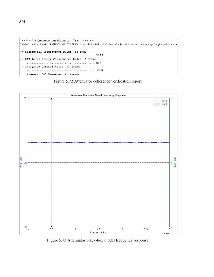
374
Figure 5.72 Attenuator coherence verification report
Figure 5.73 Attenuator black-box model frequency response
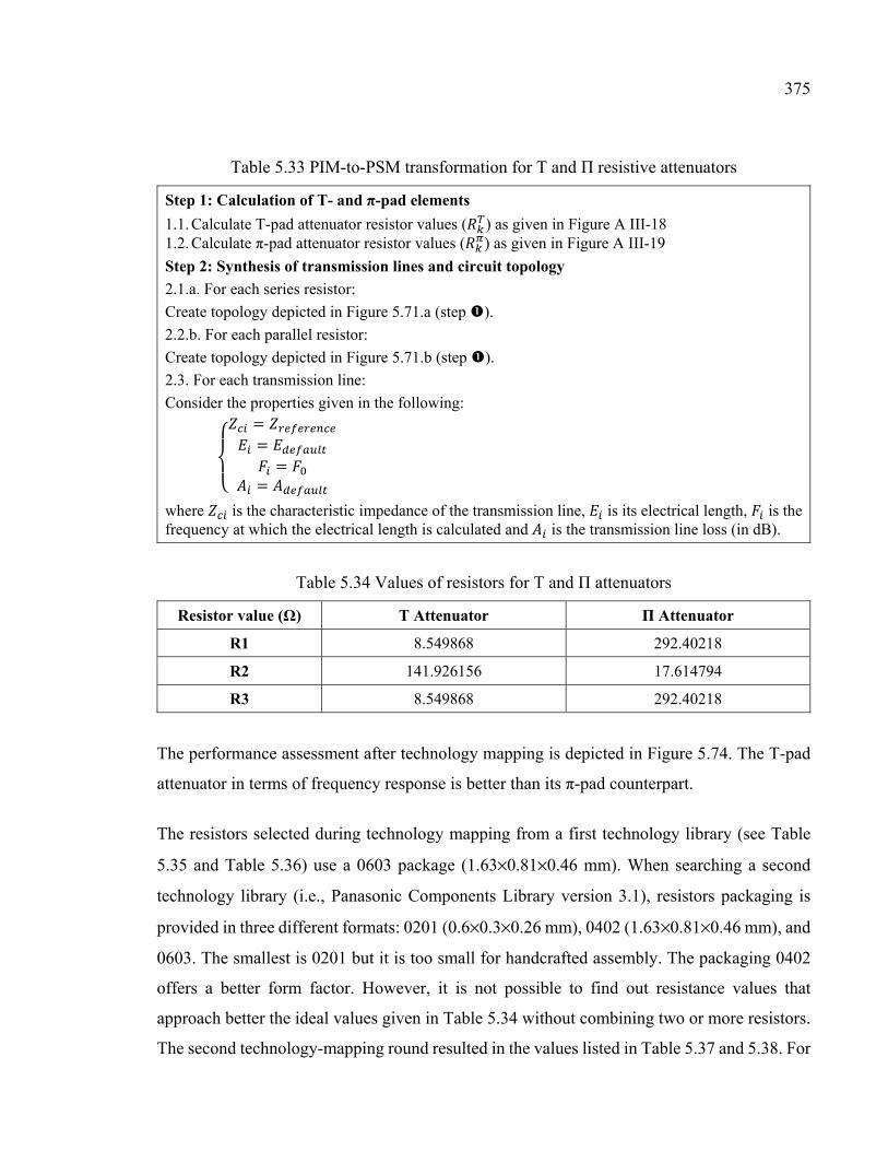
375
Table 5.33 PIM-to-PSM transformation for T and Π resistive attenuators
Step 1: Calculation of T- and π-pad elements
1.1. Calculate T-pad attenuator resistor values ( ) as given in Figure A III-18 1.2. Calculate π-pad attenuator resistor values ( ) as given in Figure A III-19
Step 2: Synthesis of transmission lines and circuit topology
2.1.a. For each series resistor:
Create topology depicted in Figure 5.71.a (step ).
2.2.b. For each parallel resistor:
Create topology depicted in Figure 5.71.b (step ).
2.3. For each transmission line:
Consider the properties given in the following: == ==
where is the characteristic impedance of the transmission line, is its electrical length, is the frequency at which the electrical length is calculated and is the transmission line loss (in dB).
Table 5.34 Values of resistors for T and Π attenuators
Resistor value (Ω) T Attenuator Π Attenuator
R1 8.549868 292.40218
R2 141.926156 17.614794
R3 8.549868 292.40218
The performance assessment after technology mapping is depicted in Figure 5.74. The T-pad
attenuator in terms of frequency response is better than its π-pad counterpart.
The resistors selected during technology mapping from a first technology library (see Table
5.35 and Table 5.36) use a 0603 package (1.63×0.81×0.46 mm). When searching a second
technology library (i.e., Panasonic Components Library version 3.1), resistors packaging is
provided in three different formats: 0201 (0.6×0.3×0.26 mm), 0402 (1.63×0.81×0.46 mm), and
0603. The smallest is 0201 but it is too small for handcrafted assembly. The packaging 0402
offers a better form factor. However, it is not possible to find out resistance values that
approach better the ideal values given in Table 5.34 without combining two or more resistors.
The second technology-mapping round resulted in the values listed in Table 5.37 and 5.38. For
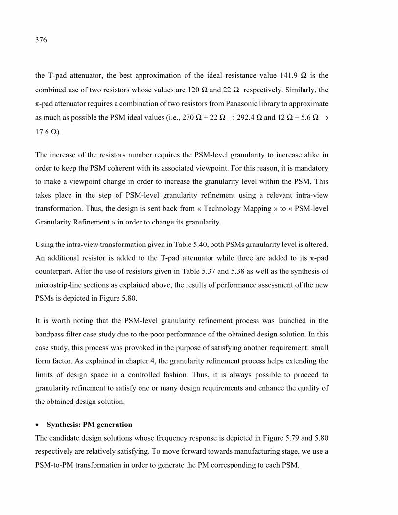
376
the T-pad attenuator, the best approximation of the ideal resistance value 141.9 Ω is the
combined use of two resistors whose values are 120 Ω and 22 Ω respectively. Similarly, the
π-pad attenuator requires a combination of two resistors from Panasonic library to approximate
as much as possible the PSM ideal values (i.e., 270 Ω + 22 Ω → 292.4 Ω and 12 Ω + 5.6 Ω →
17.6 Ω).
The increase of the resistors number requires the PSM-level granularity to increase alike in
order to keep the PSM coherent with its associated viewpoint. For this reason, it is mandatory
to make a viewpoint change in order to increase the granularity level within the PSM. This
takes place in the step of PSM-level granularity refinement using a relevant intra-view
transformation. Thus, the design is sent back from « Technology Mapping » to « PSM-level
Granularity Refinement » in order to change its granularity.
Using the intra-view transformation given in Table 5.40, both PSMs granularity level is altered.
An additional resistor is added to the T-pad attenuator while three are added to its π-pad
counterpart. After the use of resistors given in Table 5.37 and 5.38 as well as the synthesis of
microstrip-line sections as explained above, the results of performance assessment of the new
PSMs is depicted in Figure 5.80.
It is worth noting that the PSM-level granularity refinement process was launched in the
bandpass filter case study due to the poor performance of the obtained design solution. In this
case study, this process was provoked in the purpose of satisfying another requirement: small
form factor. As explained in chapter 4, the granularity refinement process helps extending the
limits of design space in a controlled fashion. Thus, it is always possible to proceed to
granularity refinement to satisfy one or many design requirements and enhance the quality of
the obtained design solution.
• Synthesis: PM generation
The candidate design solutions whose frequency response is depicted in Figure 5.79 and 5.80
respectively are relatively satisfying. To move forward towards manufacturing stage, we use a
PSM-to-PM transformation in order to generate the PM corresponding to each PSM.
377
Figure 5.74 A comparison between the T and Π attenuators in terms of frequency response and noise levels (at the end of step 1 of the PIM-to-PSM transformation)
Using a commercial design package (i.e., ADS), we transform both PSMs into physical
layouts. The PM corresponding to the PSM resulting from the initial technology mapping is
illustrated in Figure 5.81. The PM corresponding to the PSM resulting from granularity
refinement is depicted in Figure 5.82. It is trivial to note the effect of PSM-level granularity
refinement between both PMs. For instance, an additional resistor (green colored) and an extra
microstrip section (red colored) are observed in the T-pad attenuator of Figure 5.82.a which
brings the total number of resistors to four (against three in the original attenuator PM
illustrated in Figure 5.81.a). This observation is also valid to the π-pad attenuator PMs (Figure
5.82.b versus Figure 5.81.b). In addition, the frequency response of the generated PMs is
illustrated in Figure 5.83 (original PSM) and 5.84 (PSM resulting from granularity refinement).
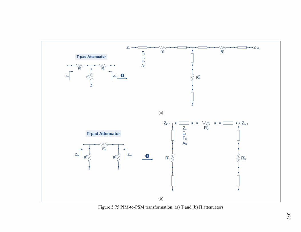
T-pad Attenuator
R2
R1 R3
ZoutZin
T
T
T
Zin Zout
R1 R3
R2
T
T
TZc
EL
F0
A0
(a)
R1 R3
R2
Zin Zoutπ
π
π
Π-pad Attenuator
Zin Zout
R1 R3
R2Zc
EL
F0
A0
π
π
π
(b)
Figure 5.75 PIM-to-PSM transformation: (a) T and (b) Π attenuators
377
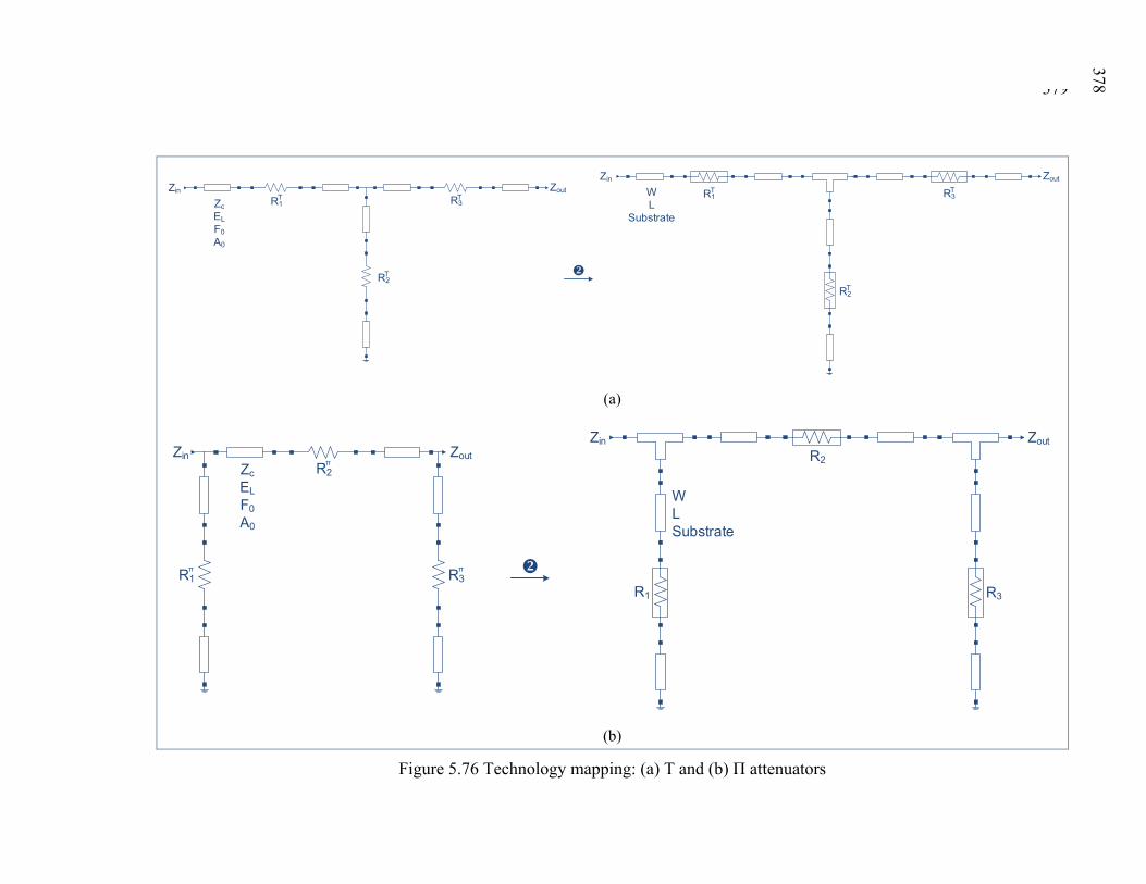
379
Zin Zout
R1 R3
R2
T
T
TZc
EL
F0
A0
Zin Zout
R1 R3
R2
T
T
TWL
Substrate
(a)
Zin Zout
R1 R3
R2Zc
EL
F0
A0
π
π
π
Zin Zout
R1 R3
R2
WLSubstrate
(b)
Figure 5.76 Technology mapping: (a) T and (b) Π attenuators
378
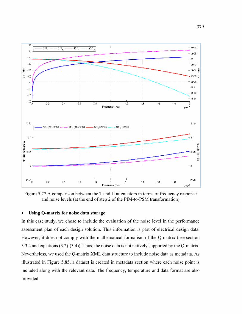
Figure 5.77 A comparison between the T and Π attenuators in terms of frequency response and noise levels (at the end of step 2 of the PIM-to-PSM transformation)
• Using Q-matrix for noise data storage
In this case study, we chose to include the evaluation of the noise level in the performance
assessment plan of each design solution. This information is part of electrical design data.
However, it does not comply with the mathematical formalism of the Q-matrix (see section
3.3.4 and equations (3.2)-(3.4)). Thus, the noise data is not natively supported by the Q-matrix.
Nevertheless, we used the Q-matrix XML data structure to include noise data as metadata. As
illustrated in Figure 5.85, a dataset is created in metadata section where each noise point is
included along with the relevant data. The frequency, temperature and data format are also
provided.
379
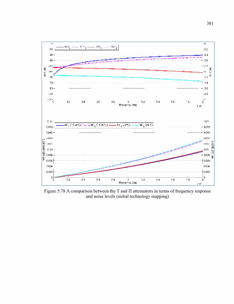
381
Figure 5.78 A comparison between the T and Π attenuators in terms of frequency response and noise levels (initial technology mapping)
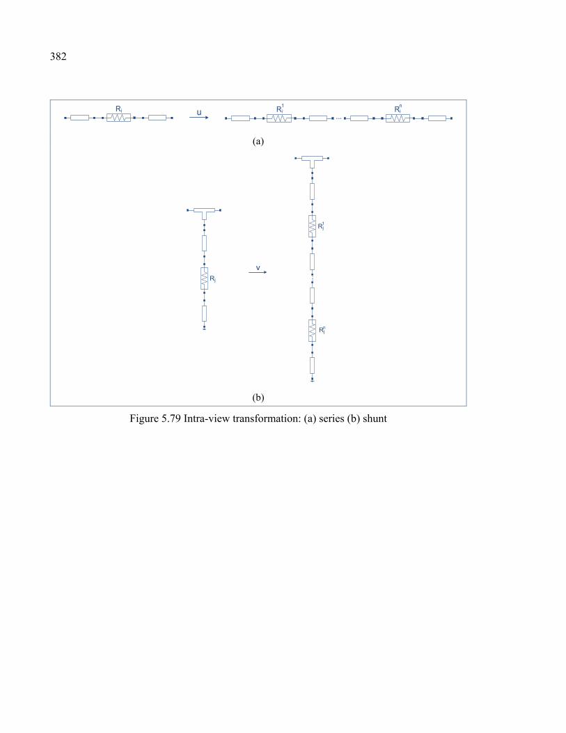
382
u ...Ri Ri
1 nRi
(a)
1
...
Rj
Rjn
Rj
v
(b)
Figure 5.79 Intra-view transformation: (a) series (b) shunt
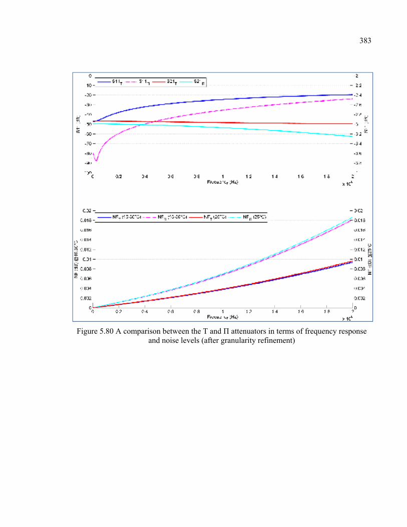
383
Figure 5.80 A comparison between the T and Π attenuators in terms of frequency response and noise levels (after granularity refinement)
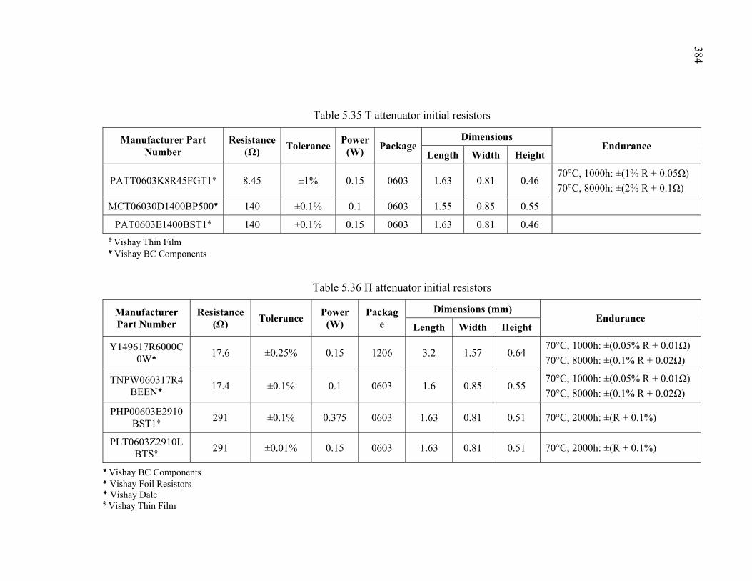
Table 5.35 T attenuator initial resistors
Manufacturer Part Number
Resistance (Ω)
TolerancePower
(W) Package
Dimensions Endurance
Length Width Height
PATT0603K8R45FGT1 8.45 ±1% 0.15 0603 1.63 0.81 0.46 70°C, 1000h: ±(1% R + 0.05Ω)
70°C, 8000h: ±(2% R + 0.1Ω)
MCT06030D1400BP500♥ 140 ±0.1% 0.1 0603 1.55 0.85 0.55
PAT0603E1400BST1 140 ±0.1% 0.15 0603 1.63 0.81 0.46 Vishay Thin Film ♥ Vishay BC Components
Table 5.36 Π attenuator initial resistors
Manufacturer Part Number
Resistance (Ω)
Tolerance Power
(W) Packag
e
Dimensions (mm) Endurance
Length Width Height
Y149617R6000C0W♠
17.6 ±0.25% 0.15 1206 3.2 1.57 0.64 70°C, 1000h: ±(0.05% R + 0.01Ω)
70°C, 8000h: ±(0.1% R + 0.02Ω)
TNPW060317R4BEEN
17.4 ±0.1% 0.1 0603 1.6 0.85 0.55 70°C, 1000h: ±(0.05% R + 0.01Ω)
70°C, 8000h: ±(0.1% R + 0.02Ω)
PHP00603E2910BST1
291 ±0.1% 0.375 0603 1.63 0.81 0.51 70°C, 2000h: ±(R + 0.1%)
PLT0603Z2910LBTS
291 ±0.01% 0.15 0603 1.63 0.81 0.51 70°C, 2000h: ±(R + 0.1%)
♥ Vishay BC Components ♠ Vishay Foil Resistors Vishay Dale Vishay Thin Film
384
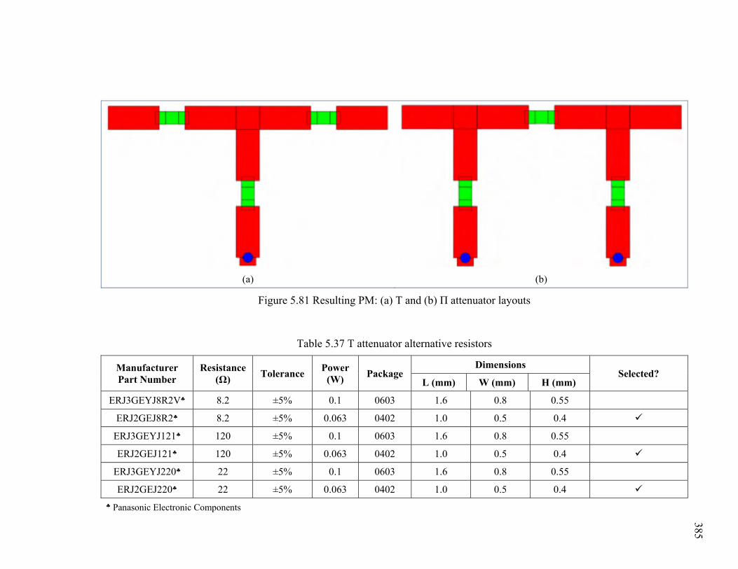
385
(a) (b)
Figure 5.81 Resulting PM: (a) T and (b) Π attenuator layouts
Table 5.37 T attenuator alternative resistors
Manufacturer Part Number
Resistance (Ω)
Tolerance Power
(W) Package
Dimensions Selected?
L (mm) W (mm) H (mm)
ERJ3GEYJ8R2V♣ 8.2 ±5% 0.1 0603 1.6 0.8 0.55
ERJ2GEJ8R2♣ 8.2 ±5% 0.063 0402 1.0 0.5 0.4
ERJ3GEYJ121♣ 120 ±5% 0.1 0603 1.6 0.8 0.55
ERJ2GEJ121♣ 120 ±5% 0.063 0402 1.0 0.5 0.4
ERJ3GEYJ220♣ 22 ±5% 0.1 0603 1.6 0.8 0.55
ERJ2GEJ220♣ 22 ±5% 0.063 0402 1.0 0.5 0.4
♣ Panasonic Electronic Components
385
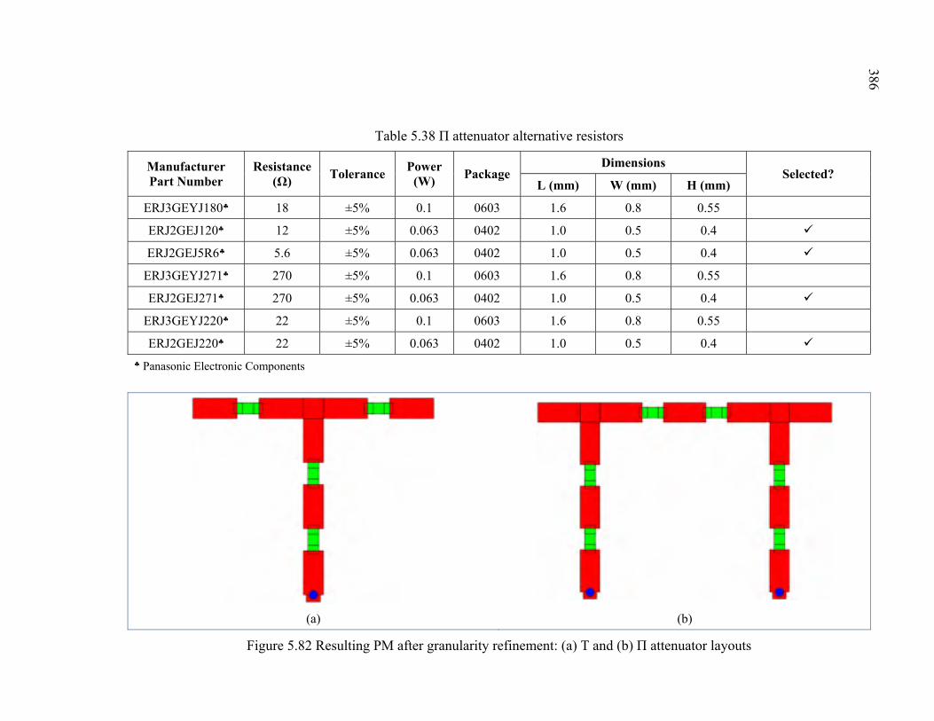
386
Table 5.38 Π attenuator alternative resistors
Manufacturer Part Number
Resistance (Ω)
Tolerance Power
(W) Package
Dimensions Selected?
L (mm) W (mm) H (mm)
ERJ3GEYJ180♣ 18 ±5% 0.1 0603 1.6 0.8 0.55
ERJ2GEJ120♣ 12 ±5% 0.063 0402 1.0 0.5 0.4
ERJ2GEJ5R6♣ 5.6 ±5% 0.063 0402 1.0 0.5 0.4
ERJ3GEYJ271♣ 270 ±5% 0.1 0603 1.6 0.8 0.55
ERJ2GEJ271♣ 270 ±5% 0.063 0402 1.0 0.5 0.4
ERJ3GEYJ220♣ 22 ±5% 0.1 0603 1.6 0.8 0.55
ERJ2GEJ220♣ 22 ±5% 0.063 0402 1.0 0.5 0.4
♣ Panasonic Electronic Components
(a) (b)
Figure 5.82 Resulting PM after granularity refinement: (a) T and (b) Π attenuator layouts
386
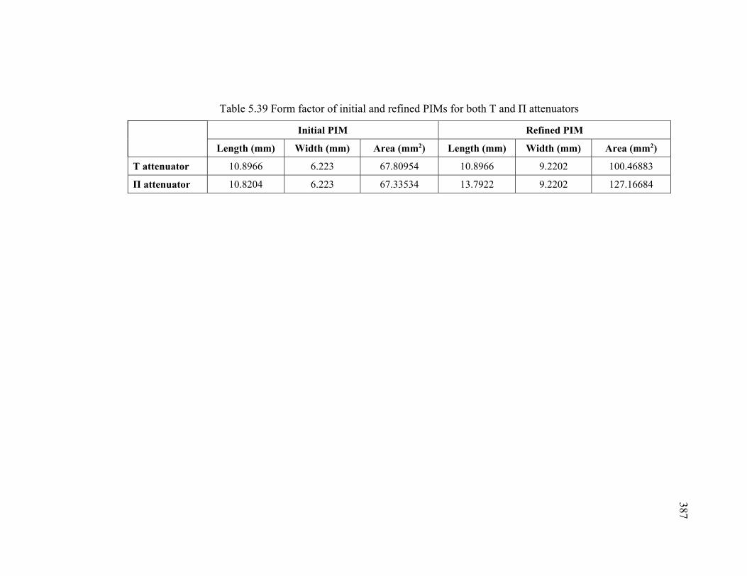
387
Table 5.39 Form factor of initial and refined PIMs for both T and Π attenuators
Initial PIM Refined PIM
Length (mm) Width (mm) Area (mm2) Length (mm) Width (mm) Area (mm2)
T attenuator 10.8966 6.223 67.80954 10.8966 9.2202 100.46883
Π attenuator 10.8204 6.223 67.33534 13.7922 9.2202 127.16684
387
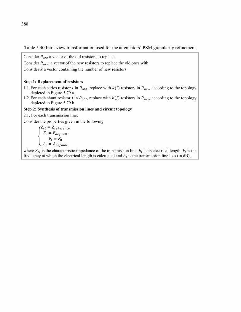
388
Table 5.40 Intra-view transformation used for the attenuators’ PSM granularity refinement
Consider a vector of the old resistors to replace
Consider a vector of the new resistors to replace the old ones with
Consider a vector containing the number of new resistors
Step 1: Replacement of resistors
1.1. For each series resistor in , replace with ( ) resistors in according to the topology depicted in Figure 5.79.a
1.2. For each shunt resistor in , replace with ( ) resistors in according to the topology depicted in Figure 5.79.b
Step 2: Synthesis of transmission lines and circuit topology
2.1. For each transmission line:
Consider the properties given in the following: == ==
where is the characteristic impedance of the transmission line, is its electrical length, is the frequency at which the electrical length is calculated and is the transmission line loss (in dB).
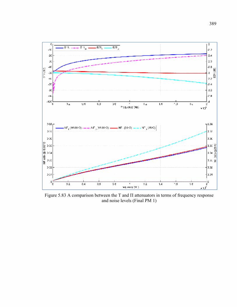
389
Figure 5.83 A comparison between the T and Π attenuators in terms of frequency response and noise levels (Final PM 1)
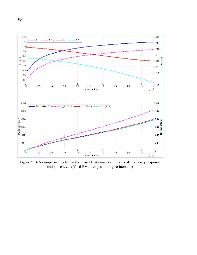
390
Figure 5.84 A comparison between the T and Π attenuators in terms of frequency response and noise levels (final PM after granularity refinement)
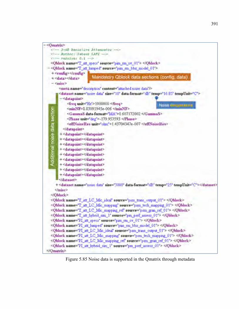
391
Figure 5.85 Noise data is supported in the Qmatrix through metadata
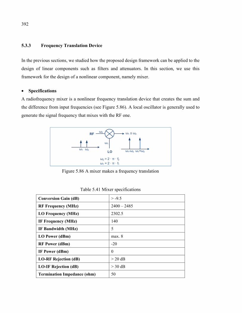
392
5.3.3 Frequency Translation Device
In the previous sections, we studied how the proposed design framework can be applied to the
design of linear components such as filters and attenuators. In this section, we use this
framework for the design of a nonlinear component, namely mixer.
• Specifications
A radiofrequency mixer is a nonlinear frequency translation device that creates the sum and
the difference from input frequencies (see Figure 5.86). A local oscillator is generally used to
generate the signal frequency that mixes with the RF one.
ω1 = 2 · π · f1
ω2 = 2 · π · f2
LO
RFω2
ω1
ω1 ± ω2
ω2ω1 ω1+ω2ω1-ω2
Figure 5.86 A mixer makes a frequency translation
Table 5.41 Mixer specifications
Conversion Gain (dB) > -9.5
RF Frequency (MHz) 2400 – 2485
LO Frequency (MHz) 2302.5
IF Frequency (MHz) 140
IF Bandwidth (MHz) 5
LO Power (dBm) max. 8
RF Power (dBm) -20
IF Power (dBm) 0
LO-RF Rejection (dB) > 20 dB
LO-IF Rejection (dB) > 30 dB
Termination Impedance (ohm) 50
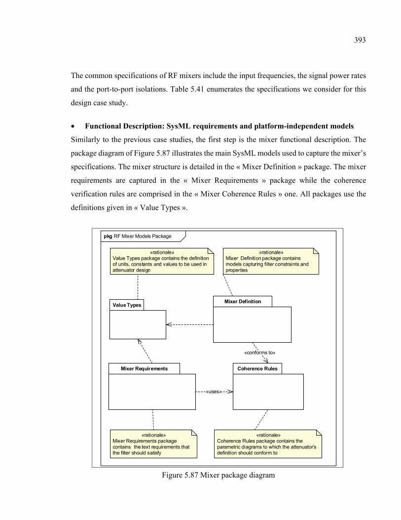
393
The common specifications of RF mixers include the input frequencies, the signal power rates
and the port-to-port isolations. Table 5.41 enumerates the specifications we consider for this
design case study.
• Functional Description: SysML requirements and platform-independent models
Similarly to the previous case studies, the first step is the mixer functional description. The
package diagram of Figure 5.87 illustrates the main SysML models used to capture the mixer’s
specifications. The mixer structure is detailed in the « Mixer Definition » package. The mixer
requirements are captured in the « Mixer Requirements » package while the coherence
verification rules are comprised in the « Mixer Coherence Rules » one. All packages use the
definitions given in « Value Types ».
Value Types
pkg RF Mixer Models Package
«rationale»Mixer Definition package contains models capturing filter constraints and properties
Mixer Definition
Mixer Requirements
«rationale»Mixer Requirements package contains the text requirements that the filter should satisfy
«rationale»Value Types package contains the definition of units, constants and values to be used in attenuator design
«rationale»Coherence Rules package contains the parametric diagrams to which the attenuator’s definition should conform to
Coherence Rules
«conforms to»
«uses»
Figure 5.87 Mixer package diagram
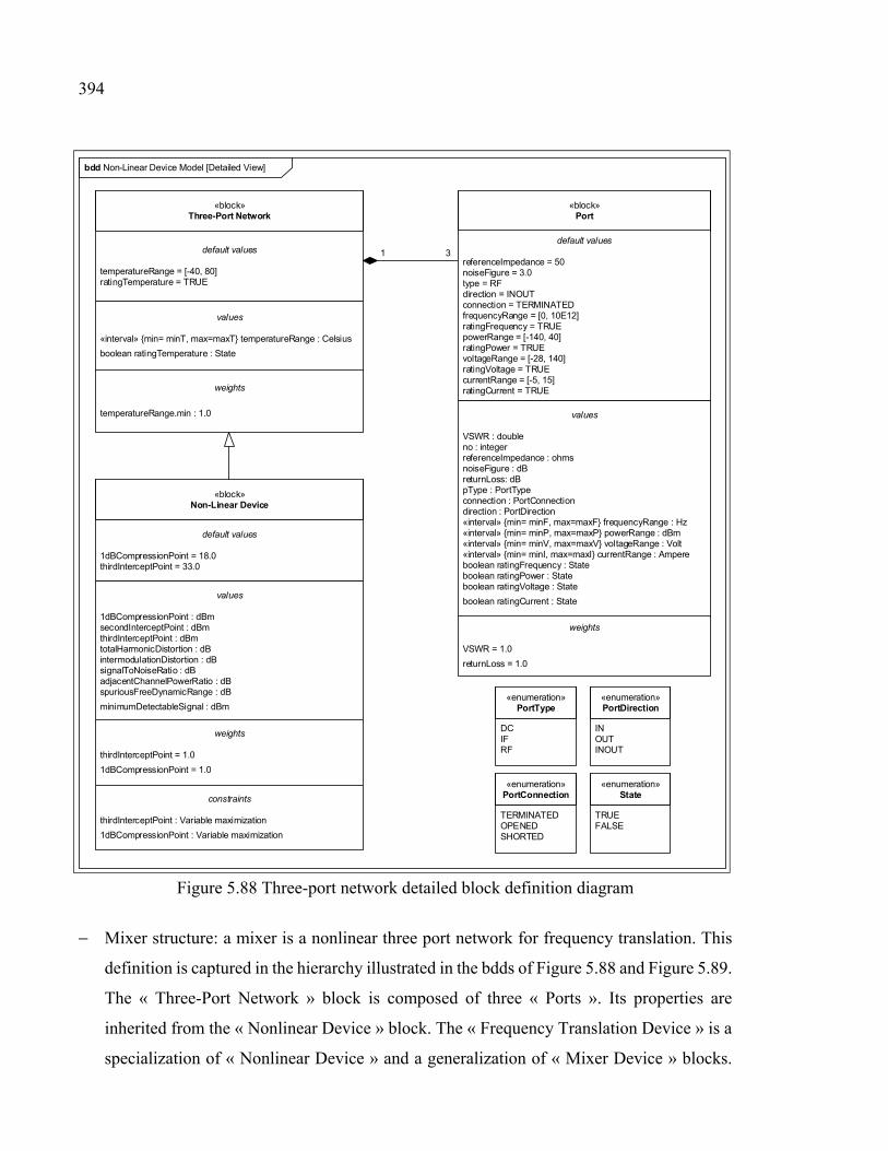
394
bdd Non-Linear Device Model [Detailed View]
«block»Three-Port Network
«enumeration»PortType
default values
temperatureRange = [-40, 80]ratingTemperature = TRUE
«block»Port
«enumeration»PortDirection
«enumeration»PortConnection
«enumeration»State
DCIFRF
INOUTINOUT
TERMINATEDOPENEDSHORTED
TRUEFALSE
values
«interval» min= minT, max=maxT temperatureRange : Celsius
boolean ratingTemperature : State
weights
temperatureRange.min : 1.0
1 3default values
referenceImpedance = 50noiseFigure = 3.0type = RFdirection = INOUTconnection = TERMINATEDfrequencyRange = [0, 10E12]ratingFrequency = TRUEpowerRange = [-140, 40]ratingPower = TRUEvoltageRange = [-28, 140]ratingVoltage = TRUEcurrentRange = [-5, 15]ratingCurrent = TRUE
values
VSWR : doubleno : integerreferenceImpedance : ohmsnoiseFigure : dBreturnLoss: dBpType : PortTypeconnection : PortConnectiondirection : PortDirection«interval» min= minF, max=maxF frequencyRange : Hz«interval» min= minP, max=maxP powerRange : dBm«interval» min= minV, max=maxV voltageRange : Volt«interval» min= minI, max=maxI currentRange : Ampereboolean ratingFrequency : Stateboolean ratingPower : Stateboolean ratingVoltage : State
boolean ratingCurrent : State
weights
VSWR = 1.0
returnLoss = 1.0
«block»Non-Linear Device
default values
1dBCompressionPoint = 18.0thirdInterceptPoint = 33.0
values
1dBCompressionPoint : dBmsecondInterceptPoint : dBmthirdInterceptPoint : dBmtotalHarmonicDistortion : dBintermodulationDistortion : dBsignalToNoiseRatio : dBadjacentChannelPowerRatio : dBspuriousFreeDynamicRange : dB
minimumDetectableSignal : dBm
weights
thirdInterceptPoint = 1.0
1dBCompressionPoint = 1.0
constraints
thirdInterceptPoint : Variable maximization
1dBCompressionPoint : Variable maximization
Figure 5.88 Three-port network detailed block definition diagram
− Mixer structure: a mixer is a nonlinear three port network for frequency translation. This
definition is captured in the hierarchy illustrated in the bdds of Figure 5.88 and Figure 5.89.
The « Three-Port Network » block is composed of three « Ports ». Its properties are
inherited from the « Nonlinear Device » block. The « Frequency Translation Device » is a
specialization of « Nonlinear Device » and a generalization of « Mixer Device » blocks.
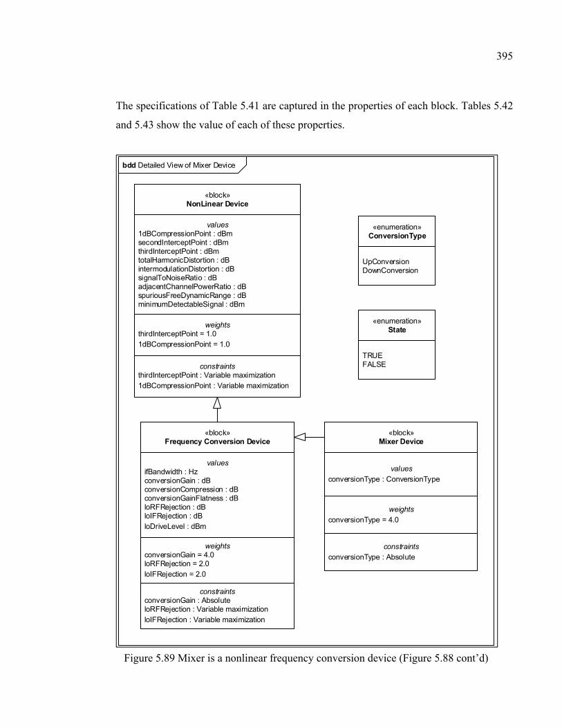
395
The specifications of Table 5.41 are captured in the properties of each block. Tables 5.42
and 5.43 show the value of each of these properties.
bdd Detailed View of Mixer Device
«block»NonLinear Device
values1dBCompressionPoint : dBmsecondInterceptPoint : dBmthirdInterceptPoint : dBmtotalHarmonicDistortion : dBintermodulationDistortion : dBsignalToNoiseRatio : dBadjacentChannelPowerRatio : dBspuriousFreeDynamicRange : dBminimumDetectableSignal : dBm
«block»Mixer Device
valuesconversionType : ConversionType
«block»Frequency Conversion Device
valuesifBandwidth : HzconversionGain : dBconversionCompression : dBconversionGainFlatness : dBloRFRejection : dBloIFRejection : dBloDriveLevel : dBm
«enumeration»ConversionType
UpConversionDownConversion
«enumeration»State
TRUEFALSE
weightsthirdInterceptPoint = 1.01dBCompressionPoint = 1.0
constraintsthirdInterceptPoint : Variable maximization1dBCompressionPoint : Variable maximization
weightsconversionGain = 4.0loRFRejection = 2.0loIFRejection = 2.0
constraintsconversionGain : AbsoluteloRFRejection : Variable maximization loIFRejection : Variable maximization
weightsconversionType = 4.0
constraintsconversionType : Absolute
Figure 5.89 Mixer is a nonlinear frequency conversion device (Figure 5.88 cont’d)
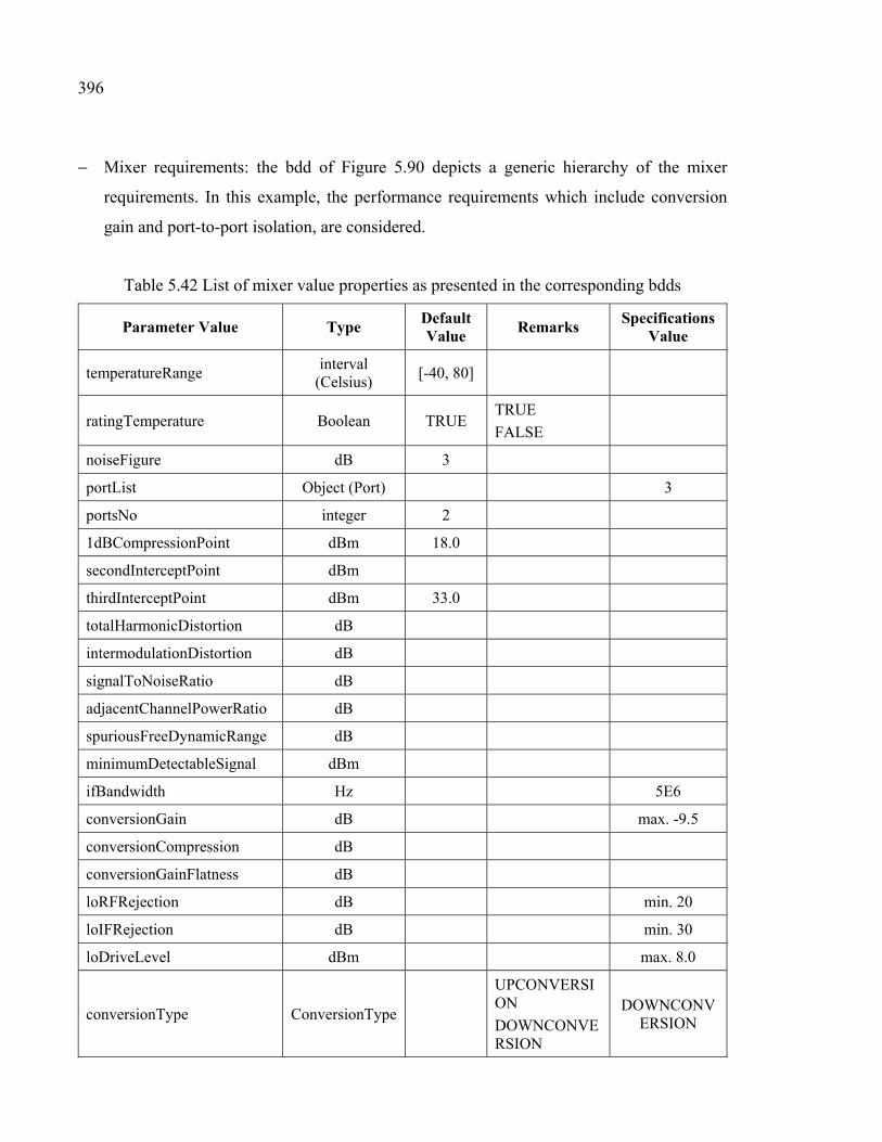
396
− Mixer requirements: the bdd of Figure 5.90 depicts a generic hierarchy of the mixer
requirements. In this example, the performance requirements which include conversion
gain and port-to-port isolation, are considered.
Table 5.42 List of mixer value properties as presented in the corresponding bdds
Parameter Value Type Default Value
Remarks Specifications
Value
temperatureRange interval
(Celsius) [-40, 80]
ratingTemperature Boolean TRUE TRUE
FALSE
noiseFigure dB 3
portList Object (Port) 3
portsNo integer 2
1dBCompressionPoint dBm 18.0
secondInterceptPoint dBm
thirdInterceptPoint dBm 33.0
totalHarmonicDistortion dB
intermodulationDistortion dB
signalToNoiseRatio dB
adjacentChannelPowerRatio dB
spuriousFreeDynamicRange dB
minimumDetectableSignal dBm
ifBandwidth Hz 5E6
conversionGain dB max. -9.5
conversionCompression dB
conversionGainFlatness dB
loRFRejection dB min. 20
loIFRejection dB min. 30
loDriveLevel dBm max. 8.0
conversionType ConversionType
UPCONVERSION
DOWNCONVERSION
DOWNCONVERSION
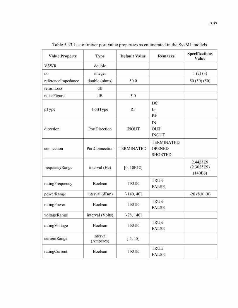
397
Table 5.43 List of mixer port value properties as enumerated in the SysML models
Value Property Type Default Value Remarks Specifications
Value
VSWR double
no integer 1 (2) (3)
referenceImpedance double (ohms) 50.0 50 (50) (50)
returnLoss dB
noiseFigure dB 3.0
pType PortType RF
DC
IF
RF
direction PortDirection INOUT
IN
OUT
INOUT
connection PortConnection TERMINATED
TERMINATED
OPENED
SHORTED
frequencyRange interval (Hz) [0, 10E12] 2.4425E9
(2.3025E9)
(140E6)
ratingFrequency Boolean TRUE TRUE
FALSE
powerRange interval (dBm) [-140, 40] -20 (8.0) (0)
ratingPower Boolean TRUE TRUE
FALSE
voltageRange interval (Volts) [-28, 140]
ratingVoltage Boolean TRUE TRUE
FALSE
currentRange interval
(Amperes) [-5, 15]
ratingCurrent Boolean TRUE TRUE
FALSE
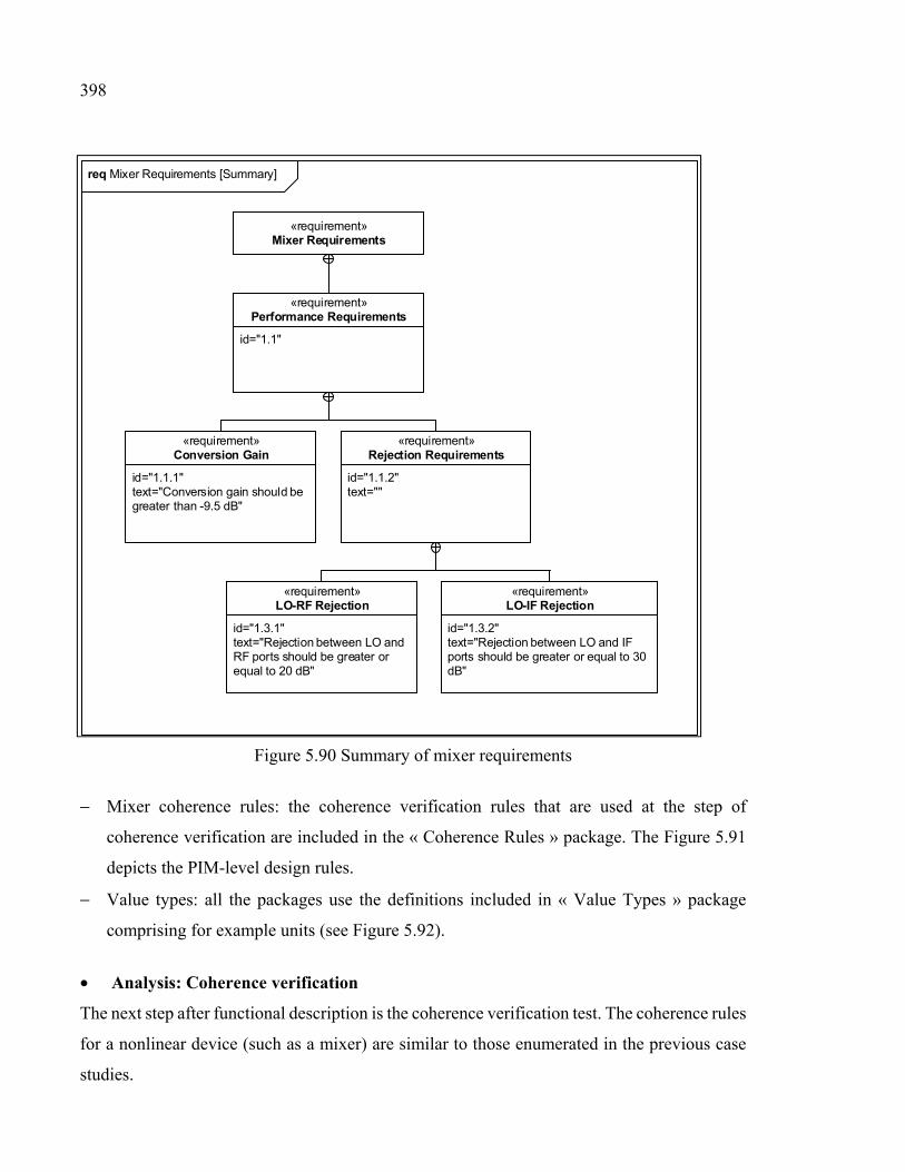
398
req Mixer Requirements [Summary]
«requirement»Mixer Requirements
id="1.3.1"text="Rejection between LO and RF ports should be greater or equal to 20 dB"
«requirement»LO-RF Rejection
id="1.3.2"text="Rejection between LO and IF ports should be greater or equal to 30 dB"
«requirement»LO-IF Rejection
id="1.1"
«requirement»Performance Requirements
id="1.1.1"text="Conversion gain should be greater than -9.5 dB"
«requirement»Conversion Gain
id="1.1.2"text=""
«requirement»Rejection Requirements
Figure 5.90 Summary of mixer requirements
− Mixer coherence rules: the coherence verification rules that are used at the step of
coherence verification are included in the « Coherence Rules » package. The Figure 5.91
depicts the PIM-level design rules.
− Value types: all the packages use the definitions included in « Value Types » package
comprising for example units (see Figure 5.92).
• Analysis: Coherence verification
The next step after functional description is the coherence verification test. The coherence rules
for a nonlinear device (such as a mixer) are similar to those enumerated in the previous case
studies.
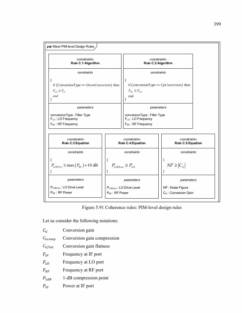
399
par Mixer PIM-level Design Rules
«constraint»Rule C.1:Algorithm
constraints
parameters
conversionType : Filter TypeFLO : LO Frequency
FRF : RF Frequency
«constraint»Rule C.2:Algorithm
constraints
parameters
conversionType : Filter TypeFLO : LO Frequency
FRF : RF Frequency
«constraint»Rule C.3:Equation
constraints
parameters
PLODrive : LO Drive Level
PRF : RF Power
«constraint»Rule C.4:Equation
constraints
parameters
PLODrive : LO Drive Level
PRF : RF Power
«constraint»Rule C.5:Equation
constraints
parameters
NF : Noise Figure
CG : Conversion Gain
( )if ConversionType then
LO IF
DownConversion
F F
end
==≤
( )if conversionType then
endRF LO
UpConversion
F F
==≤
( )max 10 dBLODrive RFP P≥ + LODrive LOP P≥ GNF C≥
Figure 5.91 Coherence rules: PIM-level design rules
Let us consider the following notations:
Conversion gain
Conversion gain compression
Conversion gain flatness
Frequency at IF port
Frequency at LO port
Frequency at RF port
1-dB compression point
Power at IF port
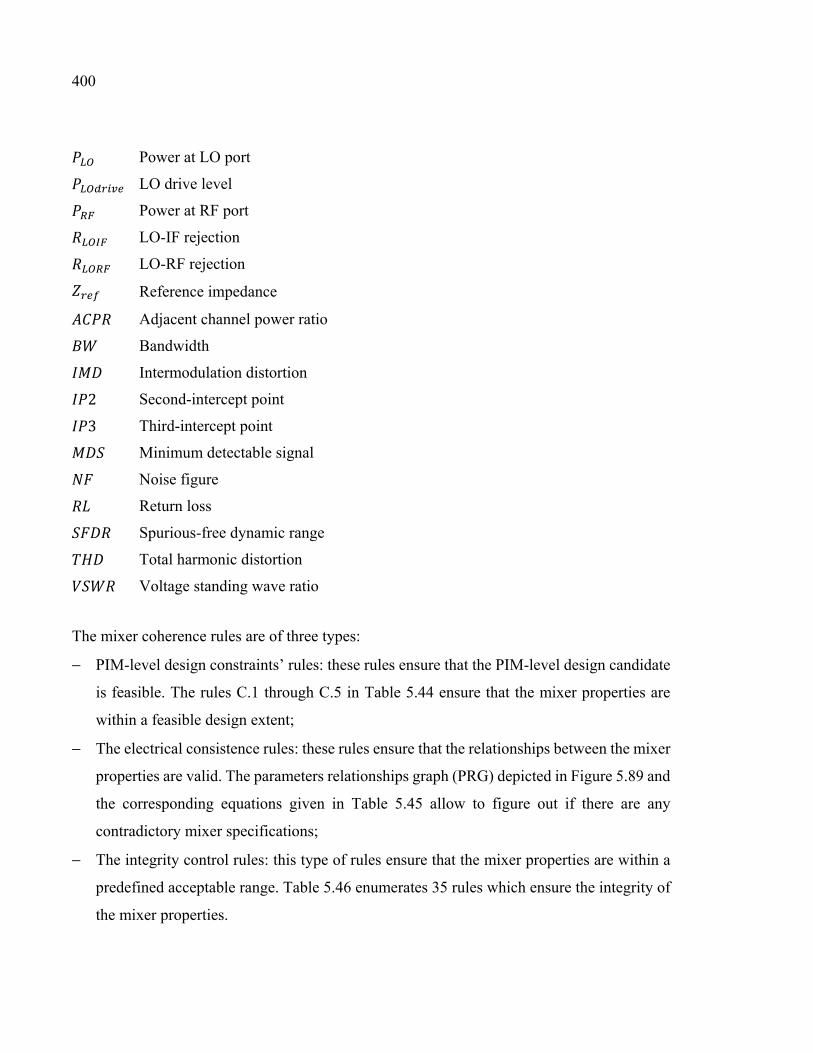
400
Power at LO port
LO drive level
Power at RF port
LO-IF rejection
LO-RF rejection
Reference impedance
Adjacent channel power ratio
Bandwidth
Intermodulation distortion 2 Second-intercept point 3 Third-intercept point
Minimum detectable signal
Noise figure
Return loss
Spurious-free dynamic range
Total harmonic distortion
Voltage standing wave ratio
The mixer coherence rules are of three types:
− PIM-level design constraints’ rules: these rules ensure that the PIM-level design candidate
is feasible. The rules C.1 through C.5 in Table 5.44 ensure that the mixer properties are
within a feasible design extent;
− The electrical consistence rules: these rules ensure that the relationships between the mixer
properties are valid. The parameters relationships graph (PRG) depicted in Figure 5.89 and
the corresponding equations given in Table 5.45 allow to figure out if there are any
contradictory mixer specifications;
− The integrity control rules: this type of rules ensure that the mixer properties are within a
predefined acceptable range. Table 5.46 enumerates 35 rules which ensure the integrity of
the mixer properties.
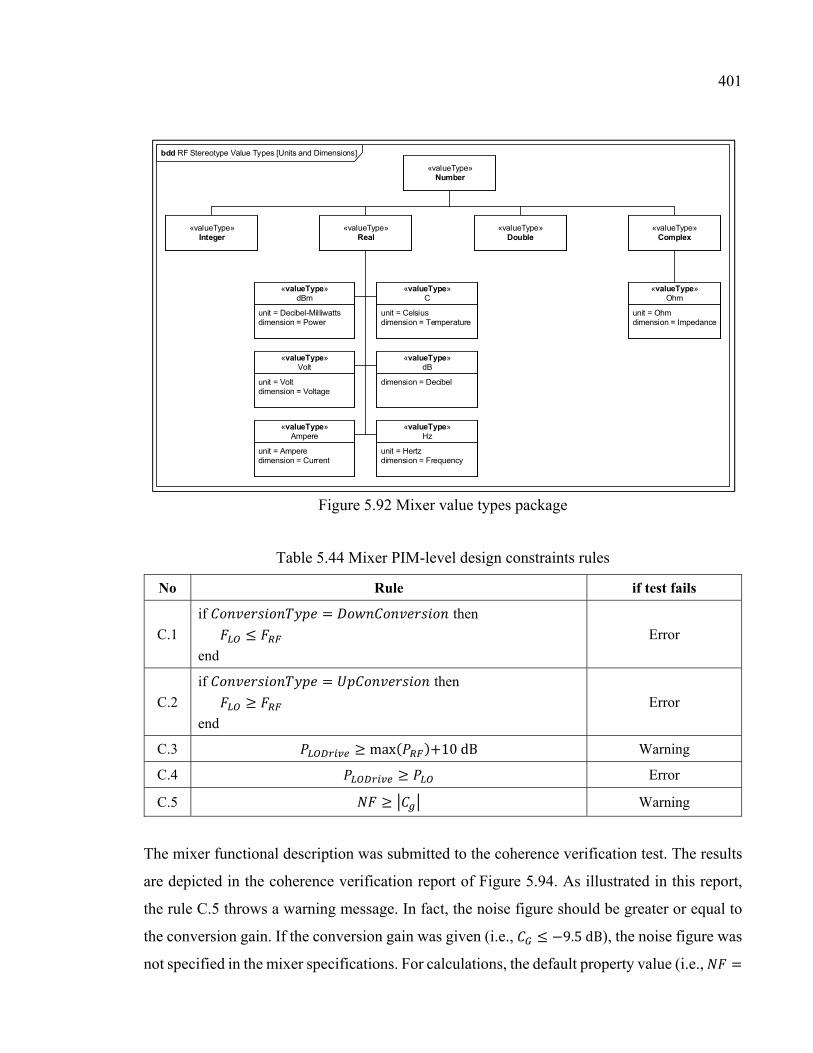
401
bdd RF Stereotype Value Types [Units and Dimensions]
«valueType»Complex
unit = Ohmdimension = Impedance
«valueType»Ohm
«valueType»Integer
«valueType»Double
«valueType»Number
«valueType»Real
unit = Celsiusdimension = Temperature
«valueType»C
dimension = Decibel
«valueType»dB
unit = Hertzdimension = Frequency
«valueType»Hz
unit = Voltdimension = Voltage
«valueType»Volt
unit = Decibel-Milliwattsdimension = Power
«valueType»dBm
unit = Amperedimension = Current
«valueType»Ampere
Figure 5.92 Mixer value types package
Table 5.44 Mixer PIM-level design constraints rules
No Rule if test fails
C.1 if = then
≤ end
Error
C.2
if = then
≥ end
Error
C.3 ≥ max( )+10dB Warning
C.4 ≥ Error
C.5 ≥ Warning
The mixer functional description was submitted to the coherence verification test. The results
are depicted in the coherence verification report of Figure 5.94. As illustrated in this report,
the rule C.5 throws a warning message. In fact, the noise figure should be greater or equal to
the conversion gain. If the conversion gain was given (i.e., ≤ −9.5dB), the noise figure was
not specified in the mixer specifications. For calculations, the default property value (i.e., =
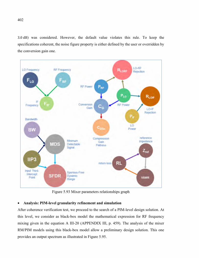
402
3.0dB) was considered. However, the default value violates this rule. To keep the
specifications coherent, the noise figure property is either defined by the user or overridden by
the conversion gain one.
Figure 5.93 Mixer parameters relationships graph
• Analysis: PIM-level granularity refinement and simulation
After coherence verification test, we proceed to the search of a PIM-level design solution. At
this level, we consider as black-box model the mathematical expression for RF frequency
mixing given in the equation A III-20 (APPENDIX III, p. 459). The analysis of the mixer
RM/PIM models using this black-box model allow a preliminary design solution. This one
provides an output spectrum as illustrated in Figure 5.95.
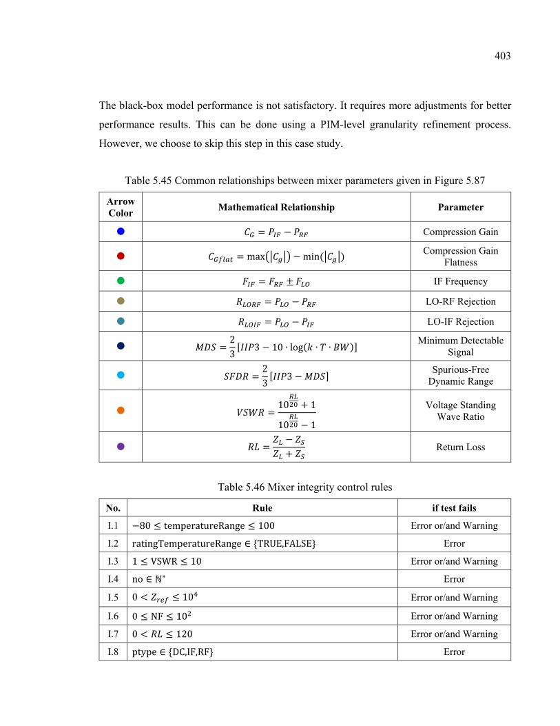
403
The black-box model performance is not satisfactory. It requires more adjustments for better
performance results. This can be done using a PIM-level granularity refinement process.
However, we choose to skip this step in this case study.
Table 5.45 Common relationships between mixer parameters given in Figure 5.87
Arrow Color
Mathematical Relationship Parameter
= − Compression Gain
= max −min( ) Compression Gain Flatness
= ± IF Frequency
= − LO-RF Rejection
= − LO-IF Rejection
= 23 [ 3 − 10 ∙ log( ∙ ∙ )] Minimum Detectable Signal
= 23 [ 3 − ] Spurious-Free Dynamic Range
= 10 + 110 − 1 Voltage Standing
Wave Ratio
= −+ Return Loss
Table 5.46 Mixer integrity control rules
No. Rule if test fails
I.1 −80 ≤ temperatureRange ≤ 100 Error or/and Warning
I.2 ratingTemperatureRange ∈ TRUE,FALSE Error
I.3 1 ≤ VSWR ≤ 10 Error or/and Warning
I.4 no ∈ ℕ∗ Error
I.5 0 < ≤ 10 Error or/and Warning
I.6 0 ≤ NF ≤ 10 Error or/and Warning
I.7 0 < ≤ 120 Error or/and Warning
I.8 ptype ∈ DC,IF,RF Error
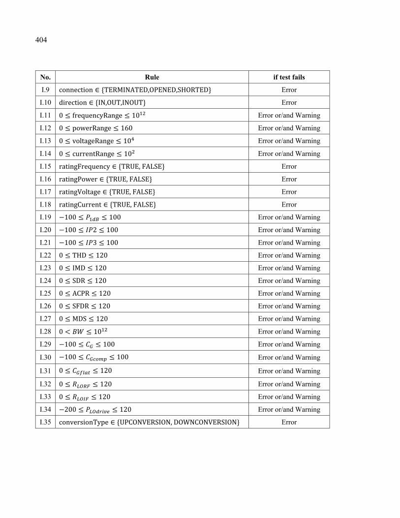
404
No. Rule if test fails
I.9 connection ∈ TERMINATED,OPENED,SHORTED Error
I.10 direction ∈ IN,OUT,INOUT Error
I.11 0 ≤ frequencyRange ≤ 10 Error or/and Warning
I.12 0 ≤ powerRange ≤ 160 Error or/and Warning
I.13 0 ≤ voltageRange ≤ 10 Error or/and Warning
I.14 0 ≤ currentRange ≤ 10 Error or/and Warning
I.15 ratingFrequency ∈ TRUE,FALSE Error
I.16 ratingPower ∈ TRUE,FALSE Error
I.17 ratingVoltage ∈ TRUE,FALSE Error
I.18 ratingCurrent ∈ TRUE,FALSE Error
I.19 −100 ≤ ≤ 100 Error or/and Warning
I.20 −100 ≤ 2 ≤ 100 Error or/and Warning
I.21 −100 ≤ 3 ≤ 100 Error or/and Warning
I.22 0 ≤ THD ≤ 120 Error or/and Warning
I.23 0 ≤ IMD ≤ 120 Error or/and Warning
I.24 0 ≤ SDR ≤ 120 Error or/and Warning
I.25 0 ≤ ACPR ≤ 120 Error or/and Warning
I.26 0 ≤ SFDR ≤ 120 Error or/and Warning
I.27 0 ≤ MDS ≤ 120 Error or/and Warning
I.28 0 < ≤ 10 Error or/and Warning
I.29 −100 ≤ ≤ 100 Error or/and Warning
I.30 −100 ≤ ≤ 100 Error or/and Warning
I.31 0 ≤ ≤ 120 Error or/and Warning
I.32 0 ≤ ≤ 120 Error or/and Warning
I.33 0 ≤ ≤ 120 Error or/and Warning
I.34 −200 ≤ ≤ 120 Error or/and Warning
I.35 conversionType ∈ UPCONVERSION,DOWNCONVERSION Error
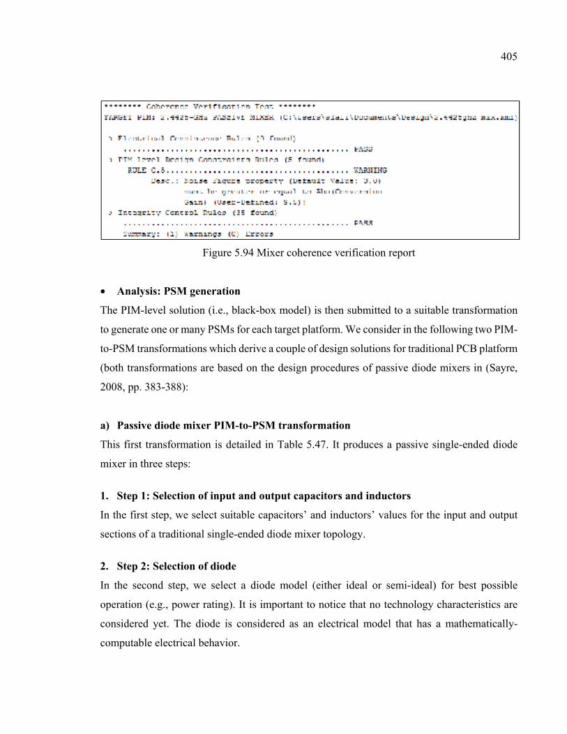
405
Figure 5.94 Mixer coherence verification report
• Analysis: PSM generation
The PIM-level solution (i.e., black-box model) is then submitted to a suitable transformation
to generate one or many PSMs for each target platform. We consider in the following two PIM-
to-PSM transformations which derive a couple of design solutions for traditional PCB platform
(both transformations are based on the design procedures of passive diode mixers in (Sayre,
2008, pp. 383-388):
a) Passive diode mixer PIM-to-PSM transformation
This first transformation is detailed in Table 5.47. It produces a passive single-ended diode
mixer in three steps:
1. Step 1: Selection of input and output capacitors and inductors
In the first step, we select suitable capacitors’ and inductors’ values for the input and output
sections of a traditional single-ended diode mixer topology.
2. Step 2: Selection of diode
In the second step, we select a diode model (either ideal or semi-ideal) for best possible
operation (e.g., power rating). It is important to notice that no technology characteristics are
considered yet. The diode is considered as an electrical model that has a mathematically-
computable electrical behavior.
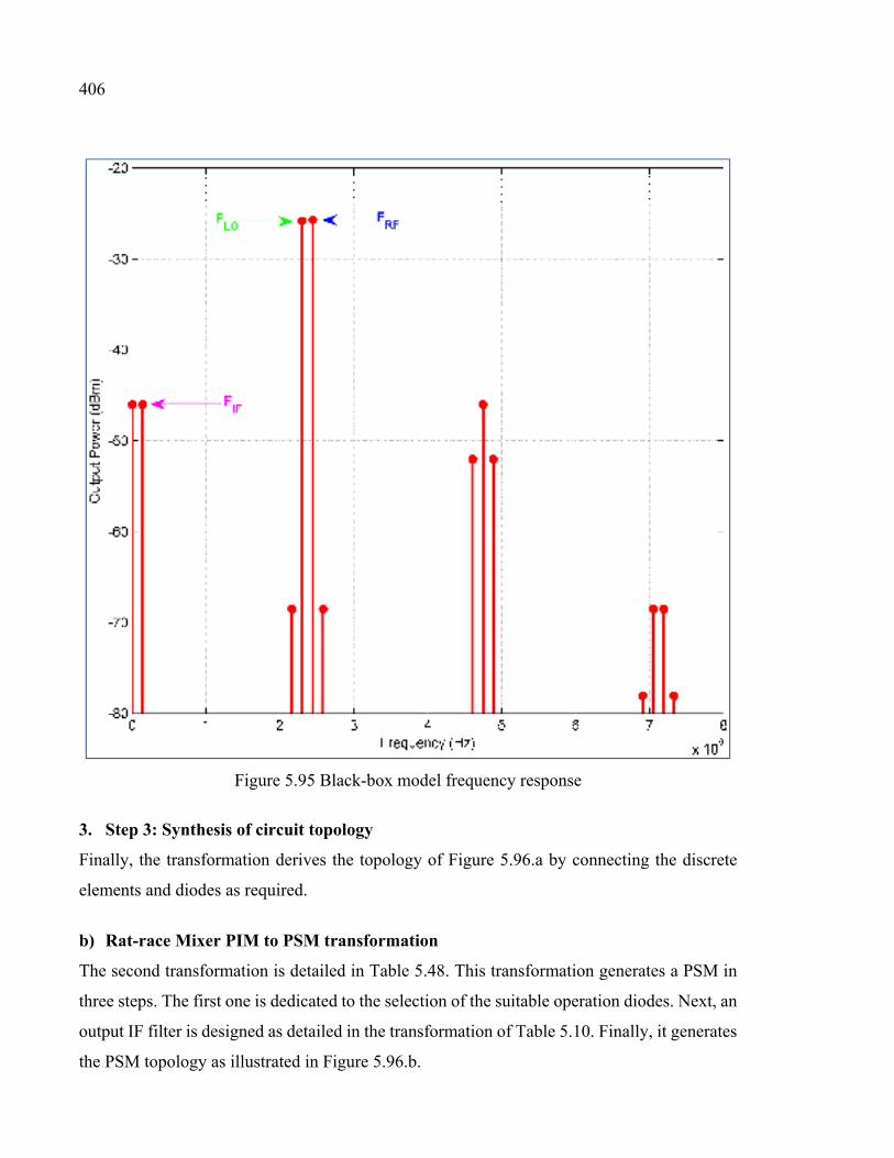
406
Figure 5.95 Black-box model frequency response
3. Step 3: Synthesis of circuit topology
Finally, the transformation derives the topology of Figure 5.96.a by connecting the discrete
elements and diodes as required.
b) Rat-race Mixer PIM to PSM transformation
The second transformation is detailed in Table 5.48. This transformation generates a PSM in
three steps. The first one is dedicated to the selection of the suitable operation diodes. Next, an
output IF filter is designed as detailed in the transformation of Table 5.10. Finally, it generates
the PSM topology as illustrated in Figure 5.96.b.
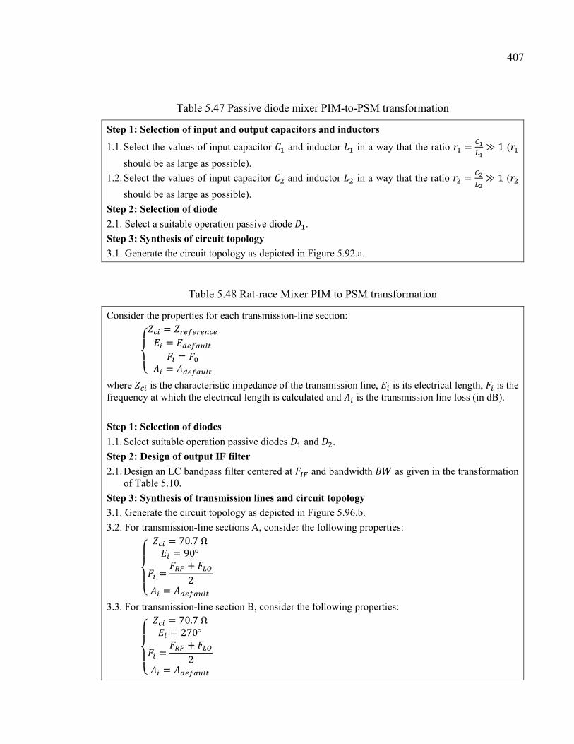
407
Table 5.47 Passive diode mixer PIM-to-PSM transformation
Step 1: Selection of input and output capacitors and inductors
1.1. Select the values of input capacitor and inductor in a way that the ratio = ≫ 1 (
should be as large as possible).
1.2. Select the values of input capacitor and inductor in a way that the ratio = ≫ 1 (
should be as large as possible).
Step 2: Selection of diode
2.1. Select a suitable operation passive diode .
Step 3: Synthesis of circuit topology
3.1. Generate the circuit topology as depicted in Figure 5.92.a.
Table 5.48 Rat-race Mixer PIM to PSM transformation
Consider the properties for each transmission-line section: == ==
where is the characteristic impedance of the transmission line, is its electrical length, is the frequency at which the electrical length is calculated and is the transmission line loss (in dB).
Step 1: Selection of diodes
1.1. Select suitable operation passive diodes and .
Step 2: Design of output IF filter
2.1. Design an LC bandpass filter centered at and bandwidth as given in the transformation of Table 5.10.
Step 3: Synthesis of transmission lines and circuit topology
3.1. Generate the circuit topology as depicted in Figure 5.96.b.
3.2. For transmission-line sections A, consider the following properties: = 70.7Ω= 90= +2=
3.3. For transmission-line section B, consider the following properties: = 70.7Ω= 270= +2=
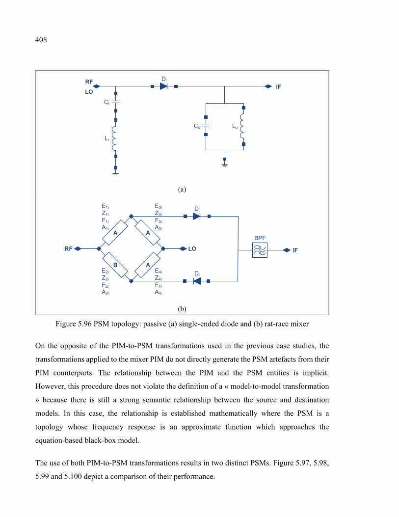
408
Lo
Di
Co
Li
Ci
RF
LOIF
(a)
Di
Di
BPF
E1i
Z1i
F1i
A1i
E2i
Z2i
F2i
A2i
E3i
Z3i
F3i
A3i
E4i
Z4i
F4i
A4i
A
A
A
B
RF LO IF
(b)
Figure 5.96 PSM topology: passive (a) single-ended diode and (b) rat-race mixer
On the opposite of the PIM-to-PSM transformations used in the previous case studies, the
transformations applied to the mixer PIM do not directly generate the PSM artefacts from their
PIM counterparts. The relationship between the PIM and the PSM entities is implicit.
However, this procedure does not violate the definition of a « model-to-model transformation
» because there is still a strong semantic relationship between the source and destination
models. In this case, the relationship is established mathematically where the PSM is a
topology whose frequency response is an approximate function which approaches the
equation-based black-box model.
The use of both PIM-to-PSM transformations results in two distinct PSMs. Figure 5.97, 5.98,
5.99 and 5.100 depict a comparison of their performance.
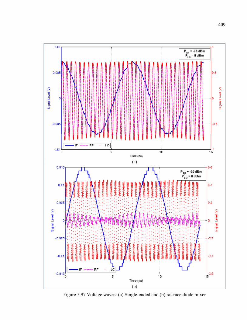
409
(a)
(b)
Figure 5.97 Voltage waves: (a) Single-ended and (b) rat-race diode mixer
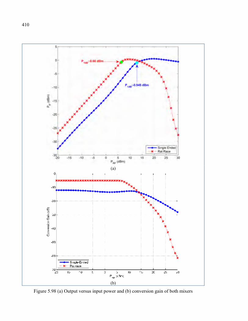
410
(a)
(b)
Figure 5.98 (a) Output versus input power and (b) conversion gain of both mixers
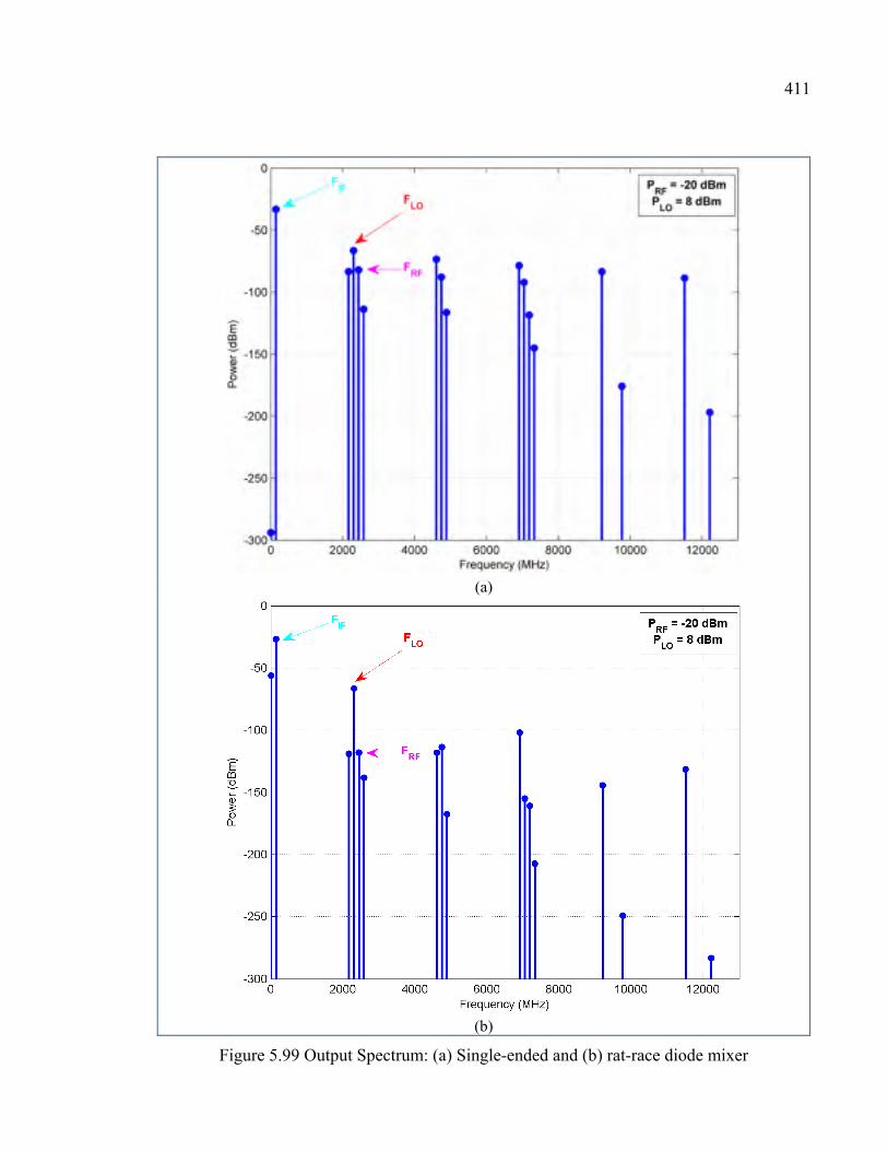
411
(a)
(b)
Figure 5.99 Output Spectrum: (a) Single-ended and (b) rat-race diode mixer
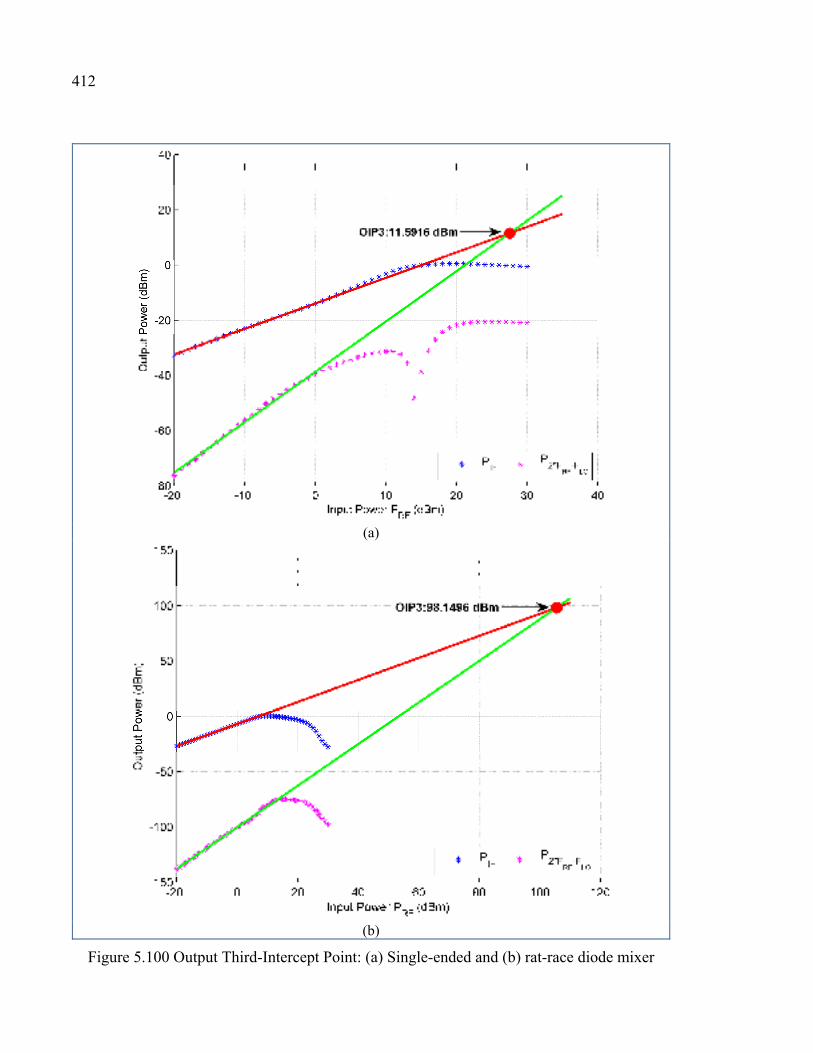
412
(a)
(b)
Figure 5.100 Output Third-Intercept Point: (a) Single-ended and (b) rat-race diode mixer
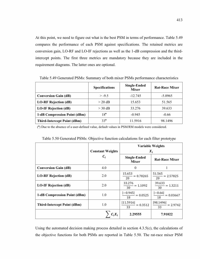
413
At this point, we need to figure out what is the best PSM in terms of performance. Table 5.49
compares the performance of each PSM against specifications. The retained metrics are
conversion gain, LO-RF and LO-IF rejections as well as the 1-dB compression and the third-
intercept points. The first three metrics are mandatory because they are included in the
requirement diagrams. The latter ones are optional.
Table 5.49 Generated PSMs: Summary of both mixer PSMs performance characteristics
Specifications Single-Ended
Mixer Rat-Race Mixer
Conversion Gain (dB) > -9.5 -12.745 -5.0965
LO-RF Rejection (dB) > 20 dB 15.653 51.565
LO-IF Rejection (dB) > 30 dB 33.276 39.633
1-dB Compression Point (dBm) 18♦ -0.945 -0.66
Third-Intercept Point (dBm) 33♦ 11.5916 98.1496
(♦) Due to the absence of a user-defined value, default values in PSM/RM models were considered.
Table 5.50 Generated PSMs: Objective function calculations for each filter prototype
Constant Weights
Variable Weights
Single-Ended Mixer
Rat-Race Mixer
Conversion Gain (dB) 4.0 0 1
LO-RF Rejection (dB) 2.0 15.65320 = 0.78265
51.56520 = 2.57825
LO-IF Rejection (dB) 2.0 33.27630 = 1.1092
39.63330 = 1.3211
1-dB Compression Point (dBm) 1.0 |−0.945|18 = 0.0525
|−0.66|18 = 0.03667
Third-Intercept Point (dBm) 1.0 |11.5916|33 = 0.3512
|98.1496|33 = 2.9742
2.29555 7.91022
Using the automated decision making process detailed in section 4.3.5(c), the calculations of
the objective functions for both PSMs are reported in Table 5.50. The rat-race mixer PSM
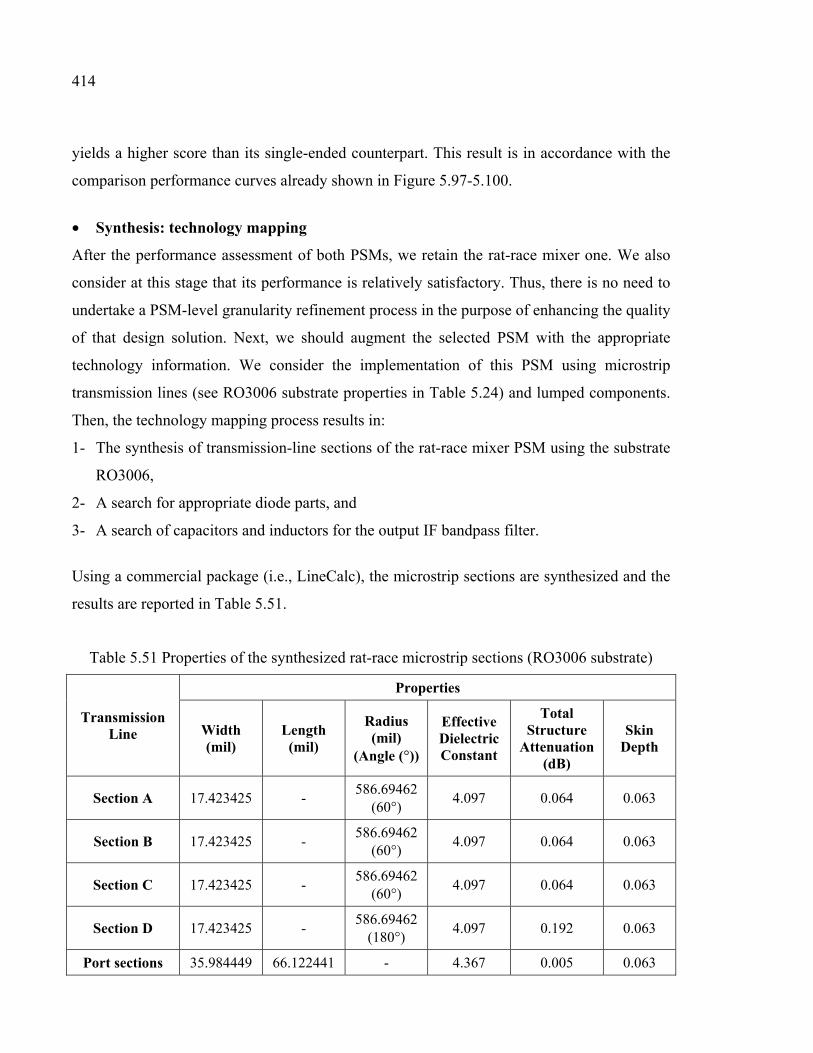
414
yields a higher score than its single-ended counterpart. This result is in accordance with the
comparison performance curves already shown in Figure 5.97-5.100.
• Synthesis: technology mapping
After the performance assessment of both PSMs, we retain the rat-race mixer one. We also
consider at this stage that its performance is relatively satisfactory. Thus, there is no need to
undertake a PSM-level granularity refinement process in the purpose of enhancing the quality
of that design solution. Next, we should augment the selected PSM with the appropriate
technology information. We consider the implementation of this PSM using microstrip
transmission lines (see RO3006 substrate properties in Table 5.24) and lumped components.
Then, the technology mapping process results in:
1- The synthesis of transmission-line sections of the rat-race mixer PSM using the substrate
RO3006,
2- A search for appropriate diode parts, and
3- A search of capacitors and inductors for the output IF bandpass filter.
Using a commercial package (i.e., LineCalc), the microstrip sections are synthesized and the
results are reported in Table 5.51.
Table 5.51 Properties of the synthesized rat-race microstrip sections (RO3006 substrate)
Transmission Line
Properties
Width (mil)
Length (mil)
Radius (mil)
(Angle (°))
Effective Dielectric Constant
Total Structure
Attenuation (dB)
Skin Depth
Section A 17.423425 - 586.69462
(60°) 4.097 0.064 0.063
Section B 17.423425 - 586.69462
(60°) 4.097 0.064 0.063
Section C 17.423425 - 586.69462
(60°) 4.097 0.064 0.063
Section D 17.423425 - 586.69462
(180°) 4.097 0.192 0.063
Port sections 35.984449 66.122441 - 4.367 0.005 0.063
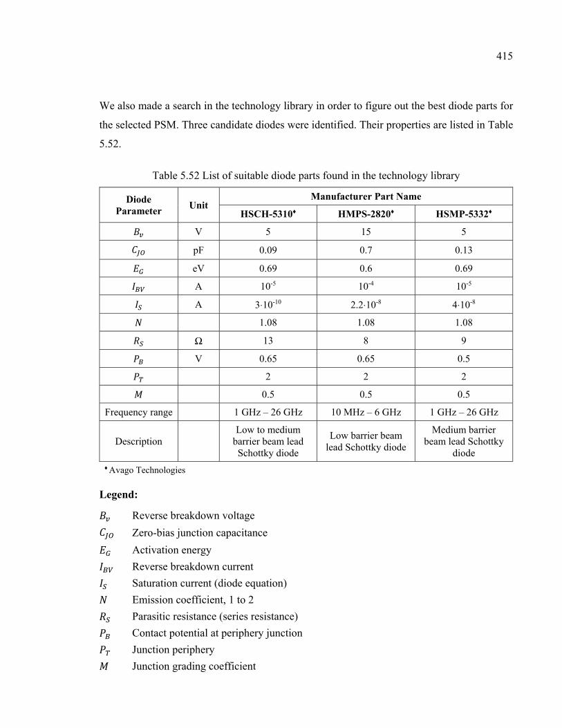
415
We also made a search in the technology library in order to figure out the best diode parts for
the selected PSM. Three candidate diodes were identified. Their properties are listed in Table
5.52.
Table 5.52 List of suitable diode parts found in the technology library
Diode Parameter
Unit Manufacturer Part Name
HSCH-5310♦ HMPS-2820♦ HSMP-5332♦
V 5 15 5
pF 0.09 0.7 0.13
eV 0.69 0.6 0.69
A 10-5 10-4 10-5
A 3⋅10-10 2.2⋅10-8 4⋅10-8
1.08 1.08 1.08
Ω 13 8 9
V 0.65 0.65 0.5
2 2 2
0.5 0.5 0.5
Frequency range 1 GHz – 26 GHz 10 MHz – 6 GHz 1 GHz – 26 GHz
Description Low to medium
barrier beam lead Schottky diode
Low barrier beam lead Schottky diode
Medium barrier beam lead Schottky
diode ♦ Avago Technologies
Legend:
Reverse breakdown voltage
Zero-bias junction capacitance
Activation energy
Reverse breakdown current
Saturation current (diode equation)
Emission coefficient, 1 to 2
Parasitic resistance (series resistance)
Contact potential at periphery junction
Junction periphery
Junction grading coefficient
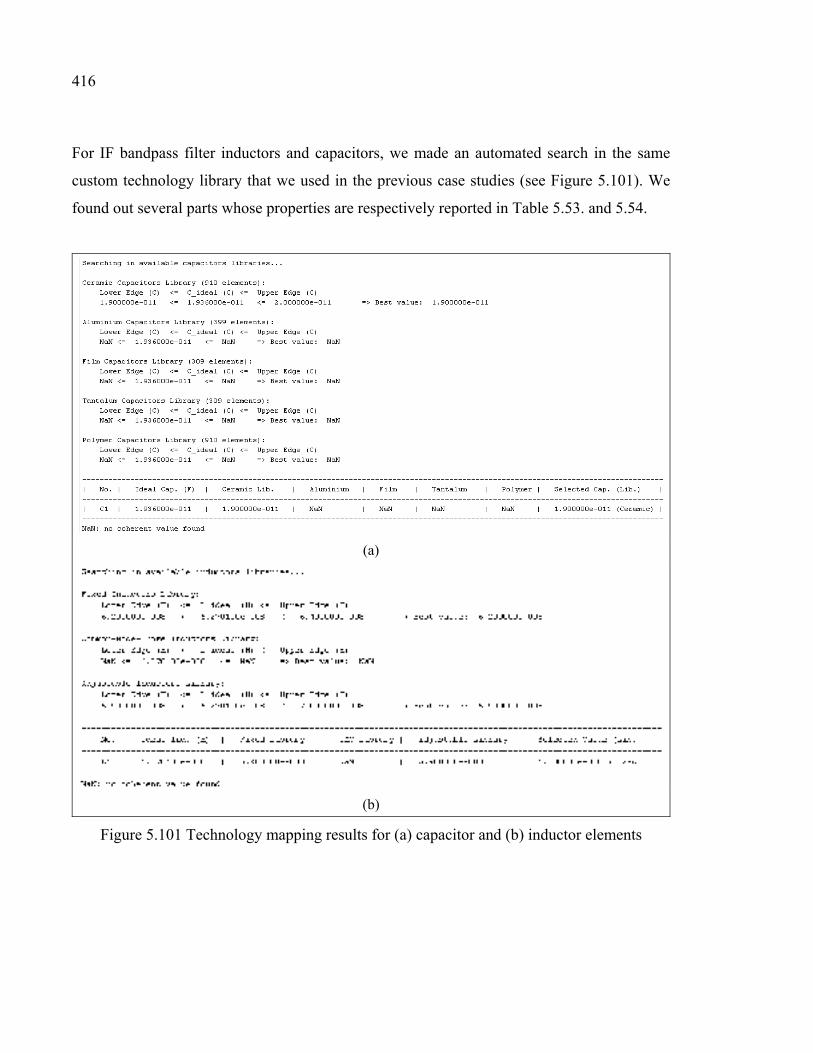
416
For IF bandpass filter inductors and capacitors, we made an automated search in the same
custom technology library that we used in the previous case studies (see Figure 5.101). We
found out several parts whose properties are respectively reported in Table 5.53. and 5.54.
(a)
(b)
Figure 5.101 Technology mapping results for (a) capacitor and (b) inductor elements
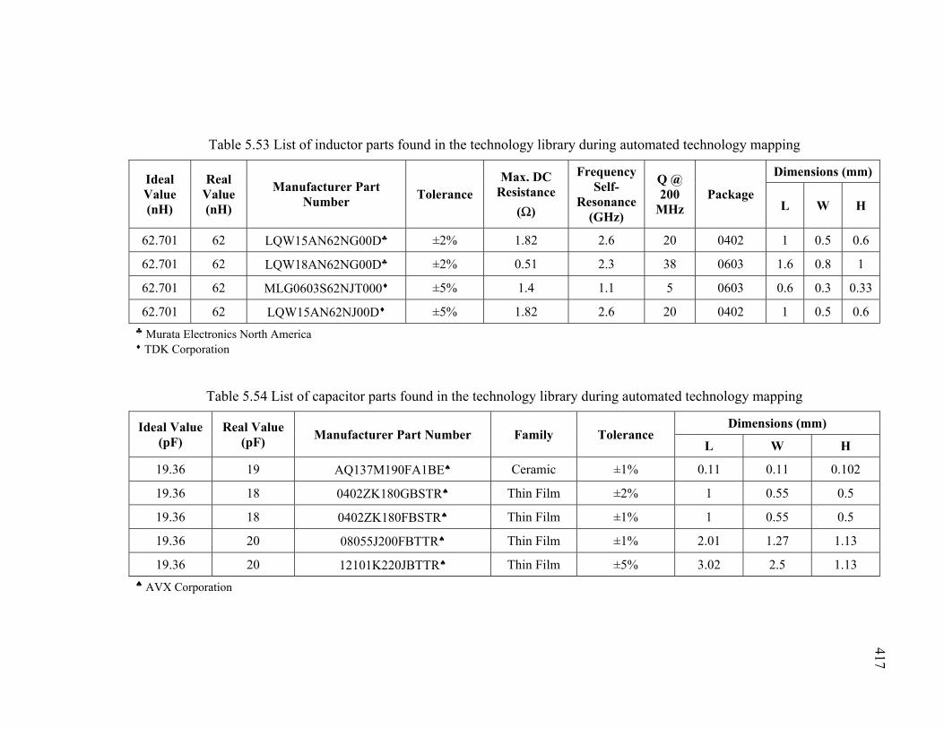
Table 5.53 List of inductor parts found in the technology library during automated technology mapping
Ideal Value (nH)
Real Value (nH)
Manufacturer Part Number
Tolerance Max. DC
Resistance
(Ω)
Frequency Self-
Resonance (GHz)
Q @ 200
MHz Package
Dimensions (mm)
L W H
62.701 62 LQW15AN62NG00D♣ ±2% 1.82 2.6 20 0402 1 0.5 0.6
62.701 62 LQW18AN62NG00D♣ ±2% 0.51 2.3 38 0603 1.6 0.8 1
62.701 62 MLG0603S62NJT000♦ ±5% 1.4 1.1 5 0603 0.6 0.3 0.33
62.701 62 LQW15AN62NJ00D♦ ±5% 1.82 2.6 20 0402 1 0.5 0.6 ♣ Murata Electronics North America ♦ TDK Corporation
Table 5.54 List of capacitor parts found in the technology library during automated technology mapping
Ideal Value (pF)
Real Value (pF)
Manufacturer Part Number Family Tolerance Dimensions (mm)
L W H
19.36 19 AQ137M190FA1BE♠ Ceramic ±1% 0.11 0.11 0.102
19.36 18 0402ZK180GBSTR♠ Thin Film ±2% 1 0.55 0.5
19.36 18 0402ZK180FBSTR♠ Thin Film ±1% 1 0.55 0.5
19.36 20 08055J200FBTTR♠ Thin Film ±1% 2.01 1.27 1.13
19.36 20 12101K220JBTTR♠ Thin Film ±5% 3.02 2.5 1.13 ♠ AVX Corporation
417
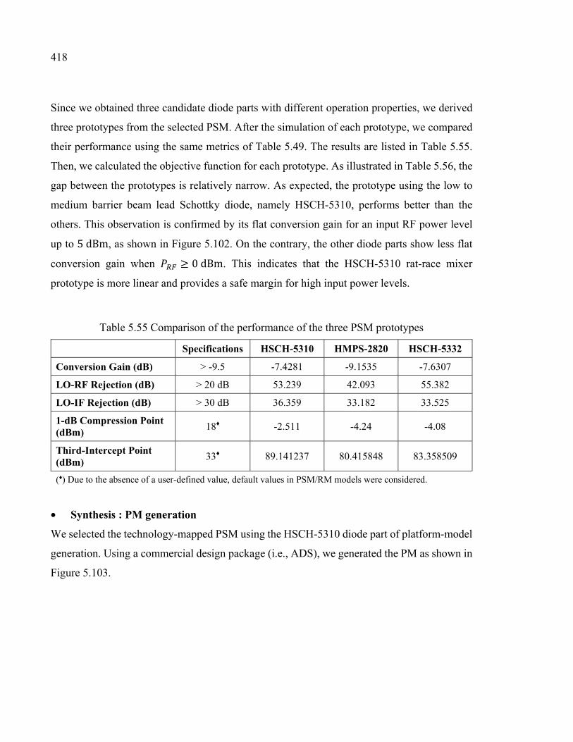
418
Since we obtained three candidate diode parts with different operation properties, we derived
three prototypes from the selected PSM. After the simulation of each prototype, we compared
their performance using the same metrics of Table 5.49. The results are listed in Table 5.55.
Then, we calculated the objective function for each prototype. As illustrated in Table 5.56, the
gap between the prototypes is relatively narrow. As expected, the prototype using the low to
medium barrier beam lead Schottky diode, namely HSCH-5310, performs better than the
others. This observation is confirmed by its flat conversion gain for an input RF power level
up to 5dBm, as shown in Figure 5.102. On the contrary, the other diode parts show less flat
conversion gain when ≥ 0dBm. This indicates that the HSCH-5310 rat-race mixer
prototype is more linear and provides a safe margin for high input power levels.
Table 5.55 Comparison of the performance of the three PSM prototypes
Specifications HSCH-5310 HMPS-2820 HSCH-5332
Conversion Gain (dB) > -9.5 -7.4281 -9.1535 -7.6307
LO-RF Rejection (dB) > 20 dB 53.239 42.093 55.382
LO-IF Rejection (dB) > 30 dB 36.359 33.182 33.525
1-dB Compression Point (dBm)
18♦ -2.511 -4.24 -4.08
Third-Intercept Point (dBm)
33♦ 89.141237 80.415848 83.358509
(♦) Due to the absence of a user-defined value, default values in PSM/RM models were considered.
• Synthesis : PM generation
We selected the technology-mapped PSM using the HSCH-5310 diode part of platform-model
generation. Using a commercial design package (i.e., ADS), we generated the PM as shown in
Figure 5.103.
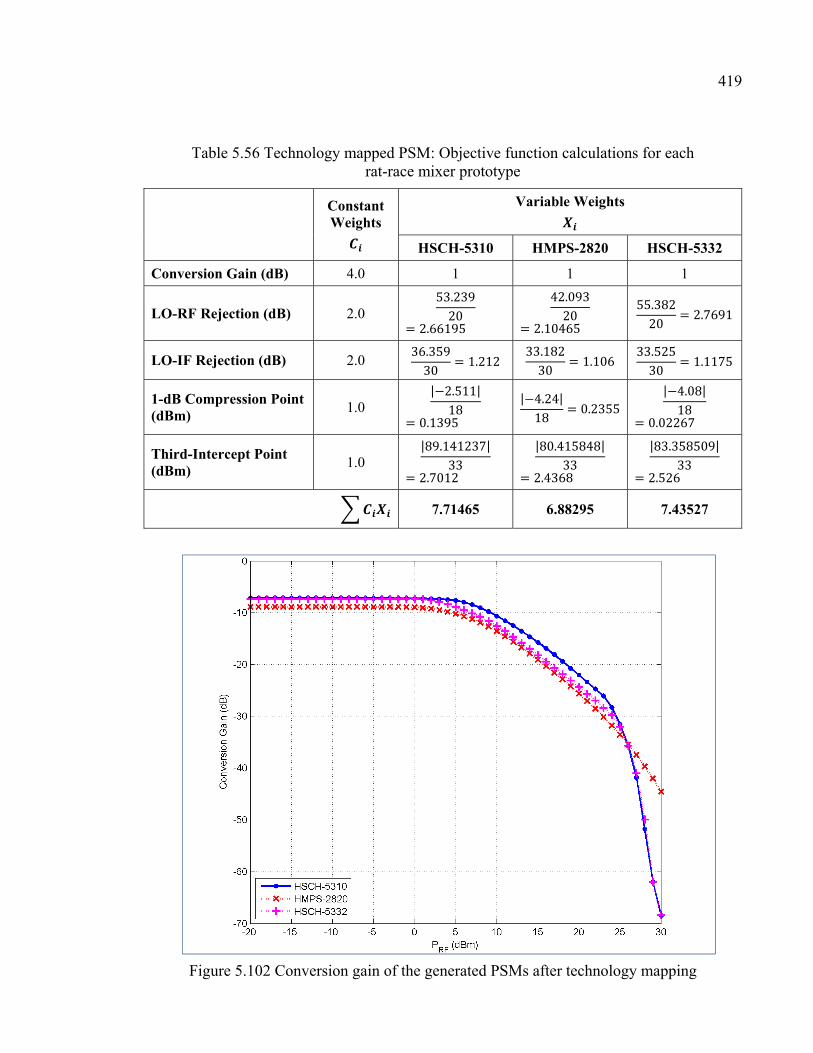
419
Table 5.56 Technology mapped PSM: Objective function calculations for each rat-race mixer prototype
Constant Weights
Variable Weights
HSCH-5310 HMPS-2820 HSCH-5332
Conversion Gain (dB) 4.0 1 1 1
LO-RF Rejection (dB) 2.0 53.23920= 2.66195
42.09320= 2.10465
55.38220 = 2.7691
LO-IF Rejection (dB) 2.0 36.35930 = 1.212
33.18230 = 1.106 33.52530 = 1.1175
1-dB Compression Point (dBm)
1.0 |−2.511|18= 0.1395
|−4.24|18 = 0.2355 |−4.08|18= 0.02267
Third-Intercept Point (dBm)
1.0 |89.141237|33= 2.7012
|80.415848|33= 2.4368
|83.358509|33= 2.526
7.71465 6.88295 7.43527
Figure 5.102 Conversion gain of the generated PSMs after technology mapping
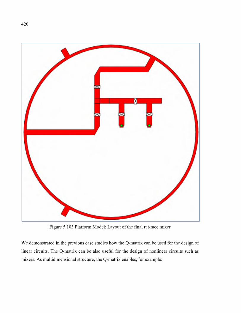
420
Figure 5.103 Platform Model: Layout of the final rat-race mixer
We demonstrated in the previous case studies how the Q-matrix can be used for the design of
linear circuits. The Q-matrix can be also useful for the design of nonlinear circuits such as
mixers. As multidimensional structure, the Q-matrix enables, for example:
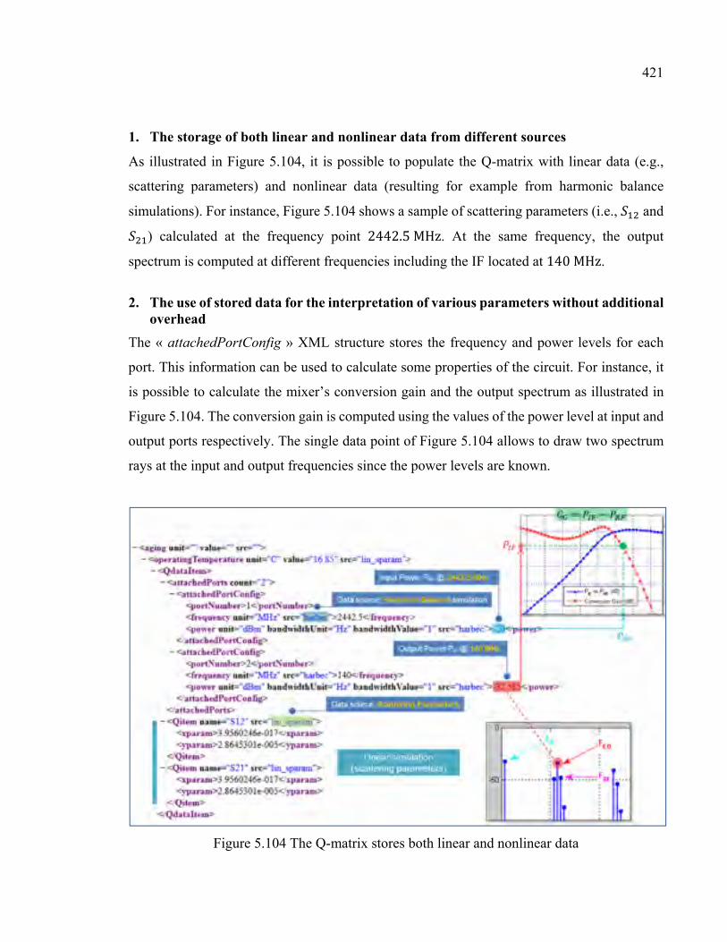
421
1. The storage of both linear and nonlinear data from different sources
As illustrated in Figure 5.104, it is possible to populate the Q-matrix with linear data (e.g.,
scattering parameters) and nonlinear data (resulting for example from harmonic balance
simulations). For instance, Figure 5.104 shows a sample of scattering parameters (i.e., and
) calculated at the frequency point 2442.5MHz. At the same frequency, the output
spectrum is computed at different frequencies including the IF located at 140MHz. 2. The use of stored data for the interpretation of various parameters without additional
overhead
The « attachedPortConfig » XML structure stores the frequency and power levels for each
port. This information can be used to calculate some properties of the circuit. For instance, it
is possible to calculate the mixer’s conversion gain and the output spectrum as illustrated in
Figure 5.104. The conversion gain is computed using the values of the power level at input and
output ports respectively. The single data point of Figure 5.104 allows to draw two spectrum
rays at the input and output frequencies since the power levels are known.
Figure 5.104 The Q-matrix stores both linear and nonlinear data
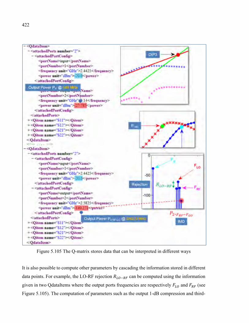
422
Figure 5.105 The Q-matrix stores data that can be interpreted in different ways
It is also possible to compute other parameters by cascading the information stored in different
data points. For example, the LO-RF rejection can be computed using the information
given in two QdataItems where the output ports frequencies are respectively and (see
Figure 5.105). The computation of parameters such as the output 1-dB compression and third-
423
intercept points require relatively more complex computations of several cascaded data points
(i.e., QdataItem).
5.4 Conclusion
In this chapter, we attempted to validate the design framework already detailed in the previous
two chapters. For this purpose, we started by reminding the basics of the design framework
which we attempted to simplify in the form of a flowchart. Then, we selected five case studies
that consisted of linear, nonlinear and system-level devices. In linear case studies, we detailed
the design process of a lumped-component bandpass filter. Then, we showed how multiple
transformations can be used to design a microstrip lowpass filter. We also demonstrated the
concurrent design of a RF attenuator using the proposed framework. In nonlinear and system-
level case studies, we designed a RF mixer and a direct-conversion receiver. For the mixer, we
presented how the framework supports nonlinear design. In direct-conversion receiver, we
showed that the framework enables the system-level analysis and design of complex front ends
using PIM-level granularity refinement. We attempted in all the previous case studies to
underline the role of the Q-matrix and how it supports linear, nonlinear and system-level design
data.
In summary, the selected case studies showed that the proposed design framework provides:
− A complete end-to-end design flow enabling concurrent design,
− A set of concepts and mechanisms that address the key design issues hampering
productivity and enhancing automation and tools interaction, and
− Foundations of an integrated design environment suitable for highly specialized tools
(electrical and beyond).
Nevertheless, there are certain gaps in tools that should be bridged in order to make the
proposed framework deployable. The required tools address various design issues:
− Functional description: intuitive tools for high-level models development (e.g., using
SysML) and visualization as well as XML generation are needed.
424
− Coherence verification: tools to handle the functional description, the definition and the
use of coherence rules are required.
− Black-box analyses: each functional description is associated in the PIM domain to one or
many black-box models. Appropriate tools are required for the definition and use of black-
box models for each functional description.
− Model-to-model transformations: the transition between models (either cross-domains or
within the same domain) is carried out using model-to-model transformations. This
requires specialized tools or/and APIs that enable the definition of transformation rules and
derive target models from source ones. The granularity refinement requires also similar
tools in both PIM and PSM domains.
− Technology mapping: the selection of technology artifacts for each model element requires
not only technology input but also automated tools to accomplish the mapping operation.
In addition to tools used for the automation of design tasks, the framework relies on the quality
of technology input required especially in PSM and PM domains. The current technology
libraries are limited and underused. The proposed framework requires technology input that
surpasses the performance and physical characterization of devices and circuits. It requires
additional data about each technology component (e.g., 3D layouts, mechanical information,
heat dissipation, power consumption and radiation profiles, etc.) in order to enable the use of
advanced techniques of assessment and specialized analysis/synthesis tools.
The selected case studies have shown that the proposed design framework is useful and
coherent. The abstraction concepts and the design mechanisms introduced by this framework
contribute to the enhancement of the RF design practice (especially in terms of productivity
and collaboration). To assure a wide adoption of this design framework, the future works
should focus on:
− The definition of an integrated design environment that implements the foundations of this
framework (especially in terms of abstraction strategy, design scheme, Q-matrix, etc.),
− The definition of a profile for the required technology input,
− The enumeration and integration of specialized tools to be used at each design step, and
− The formal validation of the Q-matrix.
CONCLUSION
This thesis is the result of a research work conducted in the context of « Intelligent RF Project
». It aimed at the exploration of new methodologies for RF circuits design. In the light of the
research activity results, this thesis intended to investigate the existing design approaches in
digital, analog/mixed-signal and RF/microwave domains. The objective was to figure out the
weaknesses and shortcomings of RF design practice considering the advances observed in
similar design domains (mainly digital and analog). Following this critical review, the
objective was to propose a new design methodology for RF devices that addresses primarily
the issues and limitations of the current design methodologies. Next, suitable mechanisms and
concepts to raise the abstraction level in RF design were proposed as well as they were
integrated within a coherent framework. Finally, the final step was the validation of the
proposed framework using selected design case studies for real applications.
In the purpose of achieving the objectives presented in the previous paragraph, this thesis was
structured into five chapters. In the first one, we focused on the background of modern RF
design practice. Thus, we briefly highlighted the evolution of wireless and mobile
communications from both historical and economic perspectives. Then, we discussed the
future trends in that domain and their expected impact on both manufacturing technologies and
design approaches. Accordingly, we investigated the challenges in both fields and discussed
the efforts being deployed to address them. We concluded that most attention of both industry
and academia is dedicated to resolving technological issues rather than contributing to enhance
RF/microwave design approaches and reducing the disparities between the design practice in
this domain and other domains (i.e., digital and mixed-signal).
In the second chapter, we focused on the review of common design approaches used for mobile
and wireless communications design. We elaborated a comparative study of common design
approaches currently in use throughout three main domains: digital, analog/mixed-signal and
RF/microwave. This comparative study resulted in the following main observations:
− The technology homogeneity and hierarchical design observed in digital (and to some
extent, analog) domain allowed affordable design of complex chips. However, the
426
technology mix made it difficult to RF designers to come up with comparable achievements
within the same timeframe;
− While the abstraction level in digital (and to some extent, analog/mixed-signal) domain is
continuously raising, no clear abstraction levels are established in RF/microwave domain;
− Per transistor, RF designers spend several times more time than their digital counterparts.
The time-to-market and the cost of RF devices remains higher than digital chips despite
their reduced complexity.
We concluded that the disparities between digital (and analog/mixed-signal) and
RF/microwave design in terms of tools sophistication, productivity and design reuse are mostly
due to the absence of enough design abstraction in the latter.
In the third chapter, we proposed a five-step design scheme built around a multi-dimensional
data structure, namely the Q-matrix, to address the major issues we noted in the previous
chapters. This design scheme introduces new design stages such as functional description, in
the purpose of raising the abstraction level in RF design. However, the proposed design scheme
does not yet provide a complete abstraction strategy.
Consequently, we investigated in the fourth chapter the hardware abstraction strategies adopted
in various domains ranging from digital/analog design to computer systems and software
engineering. For each abstraction strategy, we particularly highlighted the impact of
abstraction on automation and complexity management. Especially, we have outlined the main
abstraction concepts recently adopted in model-driven engineering. Then, we proposed the
abstraction strategy we elaborated for RF domain. Therefore, we started with the black-box
model that we adopted for functional description. We showed that common RF devices and
systems can be modeled as black-boxes whose inputs, outputs and functionality are only
known. We demonstrated also that the black-box model can be captured using high-level
modeling languages such as SysML. Next, we introduced four distinct abstraction levels (i.e.,
atomic layer, circuit, module and system) along with five different viewpoints (i.e., physical,
electrical, structural and functional). The abstraction levels and design viewpoints are
expressed using four abstraction views (called also domains). Each view is represented by a
427
distinct model (i.e., platform, platform-specific, platform-independent and requirement
models). Each model represents the RF system at a given level of detail (abstraction level) and
from a given design viewpoint (which is a design perspective expressing a set of design
considerations).
In the following step, we focused on the mechanisms allowing the transition between the
different design views. At this regard, we introduced the concept of model-to-model
transformation (i.e., inspired from MDE) to convert a source model into another one. A model-
to-model transformation can be either cross- or intra-view depending on whether the
abstraction level is changing in the destination model or not. In addition, we defined particular
types of intra-view transformations (e.g., model bridge, granularity refinement transformation)
to enable the change of the design view without changing the design viewpoint neither the
abstraction level. The advantage of such transformations is their ability to globally enhancing
the design space exploration process without altering the abstraction level. Furthermore, we
proposed a decision making process which takes part of view model artifacts in order to
automate as much as possible the selection of the « best » design solution at each abstraction
level. Finally, we presented the SysML profile for RF devices which is a set of specialized
SysML constructs dedicated to RF design. These constructs are meant to help the designer
using SysML for functional description of RF devices and systems.
In the fifth and last chapter, we attempted to demonstrate the applicability of the theoretical
concepts presented in the third and fourth chapters. Due to the absence of formal ways for the
validation of the proposed design framework, we selected four design case studies covering
both linear and nonlinear devices. We started with recalling the main design stages of the
proposed framework and sketching a step-by-step design flowchart in order to ease the
understanding of the design process. Then, we presented the design case studies of two linear
(i.e., frequency selection and attenuation) and nonlinear (i.e., frequency translation) devices.
In each design case study, we focused particularly on the key concepts of the framework such
as functional description, coherence verification, granularity refinement and technology
mapping. The role of the Q-matrix was also underlined.
428
At the end of this thesis, it seems important to underline the following observations:
− The methodology we used to conduct this research work brings proven concepts and
techniques used in other engineering disciplines (e.g., software development) to the RF
domain. Unlike the limited proposals found in literature about the abstraction of RF devices
and already discussed in the fourth chapter, the construction of the proposed RF abstraction
strategy is original because it mixed in part, concepts from software domain with others
already adopted in digital and analog design. The subsequent challenge is to show that this
mix does not hinder the practical usability and the usefulness of the overall design
framework;
− In practice, the main limitation that faced the proposed framework remains the lack of
appropriate design tools;
− In addition to the case studies presented in this thesis, we tested the proposed framework
in other design scenarios (e.g., power division and combination device). The results are
encouraging and meet our expectations. However, we cannot definitely establish that this
methodology is fully functional in all design scenarios since our validation approach was
not formal.
Contributions
The conducted research work and this thesis contributed in various ways to the academic effort
looking at making RF design faster and easier:
− We made a recent critical review of the modern RF design practice and a comparative study
with digital, analog/mixed-signal domains. Thus, we could assess the weaknesses and
shortcomings of RF domain by putting into perspective the design practice in all these
design domains. Such up-to-date review might complete the few outdated and limited
literature reviews dealing with this topic;
− The absence of comprehensive literature review of hardware abstraction not only in RF
domain but also in other engineering domains was one of the major difficulties that we
faced in this research work. We elaborated a documented review of abstraction strategies
in various domains. This effort might be useful for any future studies in this topic;
429
− We proposed a new design scheme that reproduces the main design stages found in modern
RF design practice but raises also the design abstraction levels higher than what exists in
both industry and academia. This proposal might be a first and modest contribution to the
next-generation RF design environments;
− We built an abstraction strategy for RF hardware which includes a clear subdivision
between abstraction levels, design perspectives and representations as well as the
appropriate mechanisms to manage complexity (i.e., detail level) and moving from a source
to a destination model without compromising the design coherence. We also augmented
this strategy with a modeling platform allowing to express each aspect and a decision
making process to enhance the automation of all the design steps;
− The proposed design framework allowed to redefine RF devices and systems with respect
to their functionality, inputs and outputs. This definition allowed to categorize components
in a new fashion. The immediate advantage of this new classification is the ability to cover
almost all existing devices and systems, even those in the border between RF and other
domains;
− We introduced the Q-matrix as a multi-dimensional structure which captures electrical data
from various sources throughout different dimensions (i.e., power, frequency, temperature
and aging). The Q-matrix might be a serious candidate to replace famous data standards
such as Touchstone, citifile and P2D files;
− From practical standpoint, the proposed design framework is tool- and environment-
independent. For instance, it is possible to use any structured modeling language for
functional description. However, the efficiency of modeling activity depends on that choice
since modeling languages (either general-purpose or domain-specific) do not define
necessarily all the constructs required to capture all the aspects of RF devices. In our
approach, we chose to use open and widespread standard languages such as XML and
SysML in the aim of not only enhancing the interoperability with other environments
supporting the same languages but also to allow the integration of the framework within a
super-system design environment (e.g., in aerospace systems design, radio-communication
devices are considered as small parts of a larger system). Hence, the proposed design
430
framework may be useful to bridge the gap between RF designers and their counterparts
from other disciplines;
− The proposed framework opened the door to the automation of useful design features. For
instance, the technology mapping process allows the automated selection of devices
considering non electrical parameters (e.g., physical dimensions) to evaluate non electrical
requirements (e.g.; form factor). The availability of detailed technology information
enables the assessment of various interesting aspects (e.g., EMC, form factor, etc.) of the
design in addition to its traditional electrical performance.
Future Work
This thesis presented a preliminary work in the purpose of building a new flexible design
methodology for RF and microwave systems. We particularly highlighted the proposed design
framework’s foundations from both theoretical and practical standpoints. However, there are
still numerous enhancements that can take place. There are also several concepts that require
in-depth study in future works. We enumerate hereafter a non-exhaustive list of some
outstanding research and development topics that would be accomplished in order to bring the
proposed framework to real-world design practice:
− Extended validation work: As previously mentioned, the case studies we carried out are
probably not sufficient to prove the completeness and the suitability of the framework to
all design scenarios. Thus, there is still a need to evaluate the framework mechanisms in
more complex and varied design cases. The framework gains more maturity with more
validation effort because each of the case studies we carried out has unveiled some
weaknesses in the framework and helped us to gradually fix them. Among the case studies
that would be developed, we count multi-level analysis of complete transceiver front-ends;
− Q-matrix mathematical formalism enhancement: As illustrated in the third chapter, the Q-
matrix is a super dataset that is intended to be a compact and coherent structure to hold the
design data during and after design activity. It is based on a broad mathematical definition
that extended for instance, the definition of ports to DC domain. Currently, this definition
causes some holes in the multi-dimensional matrix (e.g., existing design tools do not
compute the signal ratio between some mixed ports such as RF and DC). The Q-matrix
431
mathematical formalism should evolve in such a way that it becomes easier to define such
ratios and fill out the existing holes. The Q-matrix requires also to be interfaced to existing
measurement instruments;
− Elaboration of an experimental design environment: Among the major challenges that
faced the elaboration of the design framework is the lack of suitable tools. We estimate that
the proposed framework cannot be fully effective unless a suitable set of tools is
implemented to give thorough guidelines to designers and support the development effort
of the entire framework. In fact, the framework requires tools for high-level modeling,
coherence rules capture and analysis, model-to-model transformation elaboration and
execution, technology mapping, decision making, data import, export and conversion, etc.
In addition, a new technology library should be architected to support the new features
such multi-criteria component search and mapping. The Q-matrix requires also a set of
tools for data interpretation and capture from concurrent design sources. All these tools
should be combined in a modern, interactive and easy-to-use integrated design
environment;
− Investigation of domain-specific modeling: We elaborated the “SysML profile for RF
devices” to introduce guidelines for high-level modeling of RF systems and devices using
SysML. The latter is a generic modeling language that was conceived for the modeling of
engineering systems. It was not exclusively dedicated to electrical systems. It would be
interesting to build up a new domain-specific modeling language that is fully dedicated to
RF and microwave systems. Such language should be lightweight, straightforward and may
be based on some salient modeling constructs already defined in SysML and other existing
languages;
− Support of non-electrical design features: We showed in the fifth chapter that the new
framework not only allows the evaluation of electrical performance of the candidate design
solutions but also other non-electrical features (e.g., form factor, EMC, etc.). A future study
may investigate which tools and which non-electrical assessments could be included in the
framework. For example, is it possible to evaluate the carbon footprint of the system under
design? Naturally, this requires the development of a specific tool that calculates the circuit
carbon footprint based on its electrical performance.

APPENDIX I
HISTORY AND ADVANTAGES OF MODERN ELECTRONIC DESIGN AUTOMATION TOOLS
I.1 Introduction
EDA tools have been evolving during decades. Today, these tools become essential for almost
all designers. In this appendix, we briefly review EDA tools history and summarize their salient
advantages in modern radio design practice.
I.2 EDA History
Historically, the EDA era started in the early 1960s by the emergence of the Design
Automation Conference in 1964. It aimed to unite industry and academia efforts for the
creation of new tools to speed up the design process (Wang, Chang et Cheng, 2009). EDA
history can be subdivided to three main eras:
1. The first generation (1964 – 1978): Until the mid-1970s, electronic design was handcrafted.
However, during this decade significant research results were published. Advances covered
various topics including circuit simulation, logic simulation and testing, wire routing, etc.
The first EDA companies appeared at the late 1960s and early 1970s (e.g., Applicon in
1969, Calma in 1970 and Computervision in 1972) (Sangiovanni-Vincentelli, 2003; Wang,
Chang et Cheng, 2009). The Electronics Research Laboratory of the University of
California, Berkeley released in 1973 an analog electronic circuit simulator called SPICE
(Simulation Program with Integrated Circuit Emphasis). The first release namely SPICE1,
was derived from a less-famous simulator called CANCER (Computer Analysis of
Nonlinear Circuits, Excluding Radiation). SPICE1 included modified nodal analysis
technique and inspired several commercial circuit simulators (e.g., PSPICE of Cadence
Design Systems);
2. The second generation (1979 – 1993): During this period, the EDA domain has known a
remarkable growth. Prominent research results covered verification and testing, layout
434
manipulation and artwork edition, logic synthesis, high-level design and hardware
description languages (HDL), etc. On the business side, many EDA companies were
founded (e.g., Daisy, Mentor and Valid in 1980-1981, Cadence in 1988) (Chen, 2009b;
Sangiovanni-Vincentelli, 2003). The first public foundry, namely MOSIS (Metal Oxide
Semiconductor Implementation Service) was created in 1981. It processed since then more
than 50000 chip designs for both industry and academia (MOSIS, 2010). The hardware
description languages VHDL (Very High-Speed Integrated Circuits Hardware Description
Language) and Verilog were respectively standardized94 in 1987 and 1995. The most
famous EDA tools emerged during the 1980s. For instance, Agilent ADS, Cadence and
Ansoft HFSS were introduced in 1985, 1988 and 1989 respectively;
3. The third generation (since 1993): From 1993, the EDA tools are being progressively
mature (Sangiovanni-Vincentelli, 2003). Tools became more efficient and ergonomic. The
design flows started to be collaborative and modular. By opposition to the first- and second-
generation tools which were respectively running on mainframes and dedicated
workstations, the third-generation EDA tools are mostly intended for individual desktop
computers. Technically, behavioral-level techniques were enhanced and system-level
design techniques were introduced. For instance, System-C emerged and C++ became
attractive for system-level designers. The mixed-signal domain has seen Verilog-AMS and
VHDL-AMS standardized in 1993 and 2005 respectively.
I.3 Key EDA Advantages
EDA tools and methodologies have been of prime importance for designers since the late
1960s. Nowadays, the circuit design and manufacturing industry (either digital, analog,
RF/microwave or mixed-signal) takes advantage of the various EDA benefits. Depending on
the design domain, these benefits include:
94 VHDL and Verilog were introduced for the first time in 1981 and 1983 respectively.
435
− Completeness: EDA tools cover almost all design stages including specification, modeling,
computer-aided design (TCAD), performance simulation, layout, fabrication, integration,
packaging, test and validation (Lin et Tong, 2011);
− Automated synthesis: High-level modeling in some domains (e.g., digital) allow automated
synthesis and verification of large-scale designs with growing complexity and mix of
technologies;
− Availability of libraries: Most design tools include technology libraries and device models
that are regularly updated and enhanced allowing designers to keep up with the progress of
fabrication processes;
− Availability of multiple simulation techniques: Some EDA tools include multi-aspect
simulation features. For example, modern radiofrequency design environments (such as
Keysight Advanced Design Systems, ADS and AWR95 Microwave Office) include
electromagnetic solvers, various time- and frequency-domain simulators for small- and
large-signal analyses, intermodulation and nonlinearities study as well as noise evaluation.
This set of tools provides the designer with valuable capabilities to easily and rapidly come
up with a design meeting the initial requirements;
− Advances in system-level design: EDA tools supporting system-level design provide good
abstraction levels allowing the masking of technology details and physical complexity.
This is useful for designers who can model and analyze several architectures and potential
design solutions and rapidly figure out if they are good candidates for a final
implementation;
− Enhanced co-simulation: Whether the design platform is the same or different, some EDA
tools can actively collaborate on real-time basis. So, a tool can be used to capture the circuit
schematic while other tools for example, co-simulate its EM behavior based on its
mechanical structure. This enables the leveraging of more circuit aspects and rapidly find
out reasonable design trade-offs. For instance, ADS can be combined with the Mathworks
95 AWR stands for Applied Wave Research. AWR is an American EDA tools editor and vendor. It was acquired by National Instruments (NI) in 2011. Nevertheless, most of its EDA products continue to be marketed as AWR products.
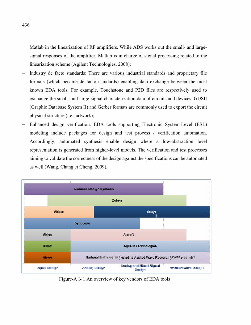
436
Matlab in the linearization of RF amplifiers. While ADS works out the small- and large-
signal responses of the amplifier, Matlab is in charge of signal processing related to the
linearization scheme (Agilent Technologies, 2008);
− Industry de facto standards: There are various industrial standards and proprietary file
formats (which became de facto standards) enabling data exchange between the most
known EDA tools. For example, Touchstone and P2D files are respectively used to
exchange the small- and large-signal characterization data of circuits and devices. GDSII
(Graphic Database System II) and Gerber formats are commonly used to export the circuit
physical structure (i.e., artwork);
− Enhanced design verification: EDA tools supporting Electronic System-Level (ESL)
modeling include packages for design and test process / verification automation.
Accordingly, automated synthesis enable design where a low-abstraction level
representation is generated from higher-level models. The verification and test processes
aiming to validate the correctness of the design against the specifications can be automated
as well (Wang, Chang et Cheng, 2009).
Figure-A I- 1 An overview of key vendors of EDA tools

437
All these benefits make EDA an essential and necessary investment, required to improve
designers’ productivity, reduce non-recurrent engineering efforts (especially in terms of time
and cost) and manage large design projects with limited human and technical resources.
I.3 Common EDA Tool Vendors
Figure-A I-1 depicts the common EDA tool vendors for digital, analog/mixed-signal and
RF/microwave design.

APPENDIX II
OVERVIEW OF SYSTEMS MODELING LANGUAGE
II.1 Introduction
With the wide adoption of the Unified Modeling Language (UML) as a standard modeling
language for software engineering, an increasing interest has emerged for the adoption of a
UML-based general-purpose modeling language dedicated to systems engineering. In 2001,
the International Council on Systems Engineering (INCOSE) formed with the OMG a special
workgroup, namely the Systems Engineering Domains Special Interest Group (SE DSIG). The
aim of SE DSIG was drafting a proposal for a new UML profile that becomes “a standard
modeling language for systems engineering to analyze, specify, design, and verify complex
systems” (OMG, 2013b). The new modeling language “is intended to enhance systems quality,
improve the ability to exchange systems engineering information amongst tools, and help
bridge the semantic gap between systems, software, and other engineering disciplines” (OMG,
2013b). The SE DSIG has rapidly seen the involvement of members from industry (e.g.,
aerospace and aeronautics, defense, communications, etc.), modeling and design tool vendors,
and academia who were interested in the definition of the new language. In 2006, the new
UML profile, namely Systems Modeling Language (SysML), was officially adopted by OMG.
Then, its version 1.0 was released in 2007. As of 2012, the OMG has released version 1.3.
II.2 SysML Paradigms
SysML, defined as an UML profile, is a graphical general-purpose modeling language. It is
not a methodology, neither a process nor a tool. To support system specification, analysis,
design, verification and validation, it was expected to alleviate the software-centric properties
of UML and provide strong semantics to express multidisciplinary engineering artefacts. At
this regard, it provided several improvements to UML paradigms:
− Strong semantics and engineering-oriented notations: SysML introduces more flexible and
expressive semantics than UML as well as new diagrams to capture requirements and
440
express system’s parametrics. This does not only allow modeling a wide range of hybrid
systems (including hardware, software, data, facilities, etc.) but also can be used for
performance analysis and simulation;
− Engineering-oriented vocabulary: As a subset of UML, SysML is a smaller language that
is easier to learn and use. It redefines most UML constructs to adapt to systems engineering.
For instance, it introduces the notion of blocks instead of classes. This kind of vocabulary,
more generic and thus more suitable for systems engineering, remains accessible to
software designers;
− Enhanced support of requirements and allocations: SysML extends the UML inherited
capability of allocations through the support of new allocation formats (e.g., tabular,
graphical, tree view, etc.). This does not only empower the capability of requirement,
functional and structural allocations but also facilitates the automation of verification and
validation processes;
− Enhanced support of domain-specific concerns: Through the adoption of the separation of
concerns concept, SysML supports models, views and viewpoints. This capability enables
the designers to address specific concerns and focus on particular system aspects that are
important from their viewpoint;
− Standard models interchange: In addition to separation of concerns and hierarchical
modeling support, SysML allows standardized data and model interchange via its
compliance with XMI and AP233 standards.
SysML was developed to enable model-based systems engineering. It was intended to provide
designers from different engineering domains with a modeling capability to create static and
dynamic models of engineering systems. It covers four main functional areas related to systems
engineering:
1. Requirements: allows not only to capture system requirements (in a contractual manner)
for different viewpoints but also to use them for verification and validation (V&V)
purposes, particularly through automated traceability and allocation mechanisms;
2. Structure: provides thorough constructs for the description of internal and external
architecture, parts and blocks of an engineering system;
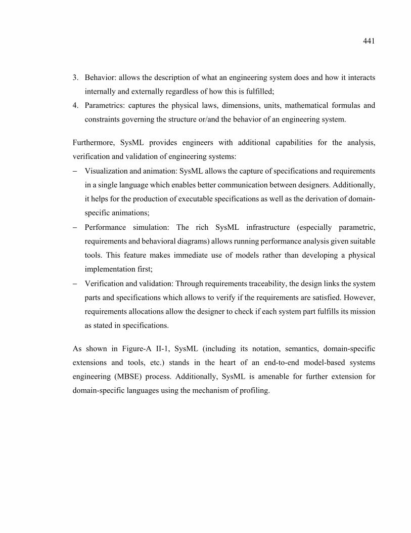
441
3. Behavior: allows the description of what an engineering system does and how it interacts
internally and externally regardless of how this is fulfilled;
4. Parametrics: captures the physical laws, dimensions, units, mathematical formulas and
constraints governing the structure or/and the behavior of an engineering system.
Furthermore, SysML provides engineers with additional capabilities for the analysis,
verification and validation of engineering systems:
− Visualization and animation: SysML allows the capture of specifications and requirements
in a single language which enables better communication between designers. Additionally,
it helps for the production of executable specifications as well as the derivation of domain-
specific animations;
− Performance simulation: The rich SysML infrastructure (especially parametric,
requirements and behavioral diagrams) allows running performance analysis given suitable
tools. This feature makes immediate use of models rather than developing a physical
implementation first;
− Verification and validation: Through requirements traceability, the design links the system
parts and specifications which allows to verify if the requirements are satisfied. However,
requirements allocations allow the designer to check if each system part fulfills its mission
as stated in specifications.
As shown in Figure-A II-1, SysML (including its notation, semantics, domain-specific
extensions and tools, etc.) stands in the heart of an end-to-end model-based systems
engineering (MBSE) process. Additionally, SysML is amenable for further extension for
domain-specific languages using the mechanism of profiling.
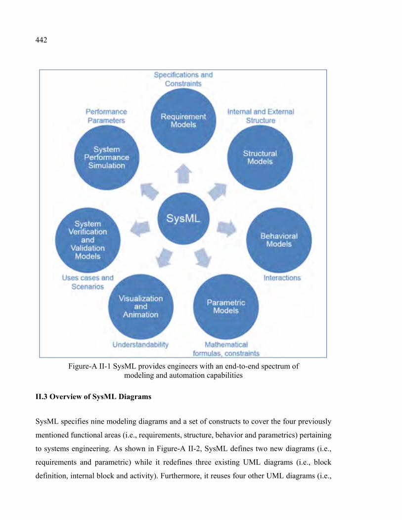
442
Figure-A II-1 SysML provides engineers with an end-to-end spectrum of modeling and automation capabilities
II.3 Overview of SysML Diagrams
SysML specifies nine modeling diagrams and a set of constructs to cover the four previously
mentioned functional areas (i.e., requirements, structure, behavior and parametrics) pertaining
to systems engineering. As shown in Figure-A II-2, SysML defines two new diagrams (i.e.,
requirements and parametric) while it redefines three existing UML diagrams (i.e., block
definition, internal block and activity). Furthermore, it reuses four other UML diagrams (i.e.,
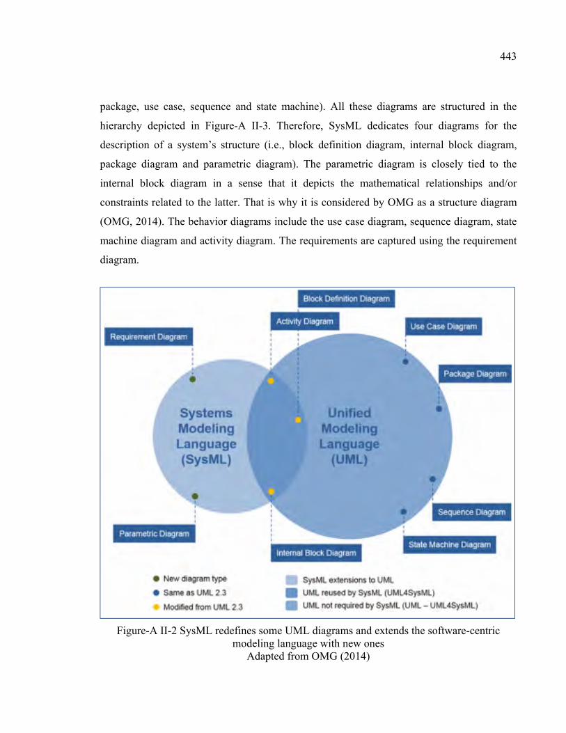
443
package, use case, sequence and state machine). All these diagrams are structured in the
hierarchy depicted in Figure-A II-3. Therefore, SysML dedicates four diagrams for the
description of a system’s structure (i.e., block definition diagram, internal block diagram,
package diagram and parametric diagram). The parametric diagram is closely tied to the
internal block diagram in a sense that it depicts the mathematical relationships and/or
constraints related to the latter. That is why it is considered by OMG as a structure diagram
(OMG, 2014). The behavior diagrams include the use case diagram, sequence diagram, state
machine diagram and activity diagram. The requirements are captured using the requirement
diagram.
Figure-A II-2 SysML redefines some UML diagrams and extends the software-centric modeling language with new ones
Adapted from OMG (2014)
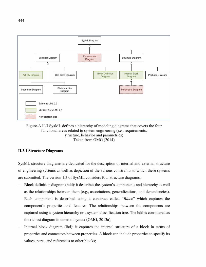
444
Same as UML 2.3
Modified from UML 2.3
New diagram type
Requirement Diagram
Block Definition Diagram
SysML Diagram
Behavior Diagram Structure Diagram
Internal Block Diagram
Package Diagram
Parametric Diagram
Activity Diagram
Sequence DiagramState Machine
Diagram
Use Case Diagram
Figure-A II-3 SysML defines a hierarchy of modeling diagrams that covers the four functional areas related to system engineering (i.e., requirements,
structure, behavior and parametrics) Taken from OMG (2014)
II.3.1 Structure Diagrams
SysML structure diagrams are dedicated for the description of internal and external structure
of engineering systems as well as depiction of the various constraints to which these systems
are submitted. The version 1.3 of SysML considers four structure diagrams:
− Block definition diagram (bdd): it describes the system’s components and hierarchy as well
as the relationships between them (e.g., associations, generalizations, and dependencies).
Each component is described using a construct called “Block” which captures the
component’s properties and features. The relationships between the components are
captured using a system hierarchy or a system classification tree. The bdd is considered as
the richest diagram in terms of syntax (OMG, 2013a);
− Internal block diagram (ibd): it captures the internal structure of a block in terms of
properties and connectors between properties. A block can include properties to specify its
values, parts, and references to other blocks;
445
− Package Diagram (pkg): it is a collection of diagram elements. The package diagram is
used to organize the system models by partitioning the model elements into (sub-)packages
and views and establishing dependencies between them (OMG, 2013a).
II.3.2 Behavior Diagrams
In SysML, behavior diagrams are used for the description of dynamic and behavioral artefacts
of an engineering system including the interactions between its components themselves or with
their environment. The version 1.3 of SysML considers four behavior diagrams:
− Activity diagram (act): it depicts the control and inputs/outputs (e.g., data, energy, material,
etc.) flow among actions and operations (i.e., activities) (OMG, 2013a);
− Sequence diagram (sd): it describes the flow of messages and interactions between
collaborating entities (including system parts or blocks and external actors);
− State machine diagram (stm): it describes the state transitions and actions that a system or
its blocks/parts should carry out in response to given events;
− Use case diagram (uc): it provides a high-level description of how the system (and its
blocks/parts) is being used by its environment actors to accomplish functionality. It is also
used to model system usage and context requirements (OMG, 2013a). In practice, it
represents the highest-level of abstraction in SysML (Holt et Perry, 2008).
II.3.3 Requirement and Parametric Diagrams
SysML has introduced two new types of diagrams (i.e., parametric and requirement diagrams)
to provide designers with mechanisms not only to express domain-specific artefacts but also
to facilitate analysis of engineering models.
− Parametric diagram (par): it is used for the definition of constraints and rules associated to
the properties of the system blocks/parts. It is also used to integrate both structure and
behavior models with engineering tools to carry out various system analyses and
simulations (e.g., performance, reliability, etc.) (OMG, 2013a) (The reader may refer to
(Peak et al., 2007a; 2007b) to learn more about how parametric diagram can be used in
real-world complex engineering systems);
446
− Requirement diagram (req): it provides modeling constructs to capture text-based
requirements into graphical, tabular or tree structure format and associate them with the
system’s structural and/or behavioral model elements using predefined relationships
(Roques, 2015).
Figure-A II-4 illustrates the nine diagrams of SysML. For an in-depth study of SysML
diagrams and constructs as well as their definition and usage, the reader may refer to
(Delligatti, 2013; Friedenthal, Moore et Steiner, 2008; Holt et Perry, 2008; OMG, 2013a;
Weilkiens, 2008).
II.3.4 Views and Viewpoints
SysML has extended the concepts of “view” and “viewpoint” from UML to support the
paradigm of concerns separation.
− View: it is a representation of a whole system (or subsystem) from the perspective of a set
of concerns (The Open Group, 2006);
− Viewpoint: it defines the perspective from which a view is taken. It is a specification of the
conventions and rules for constructing and using a view for the purpose of addressing a set
of stakeholder concerns (OMG, 2013a). For example, the selection of the information to
appear in a view is a viewpoint.
The concepts of “view” and “viewpoint” are interrelated. A view is what a stakeholder sees. A
viewpoint is the direction in which he is looking. Viewpoints are generic but views are specific.
Both concepts are important because they help partitioning the system models.
II.4 Basic Language Constructs
SysML provides a set of constructs for the modeling of engineering systems. These constructs
are used within SysML diagrams in order to describe various system aspects such as structure,
behavior, requirements, allocations and constraints. For illustration, we briefly present in the
following structural, behavioral and some crosscutting constructs.
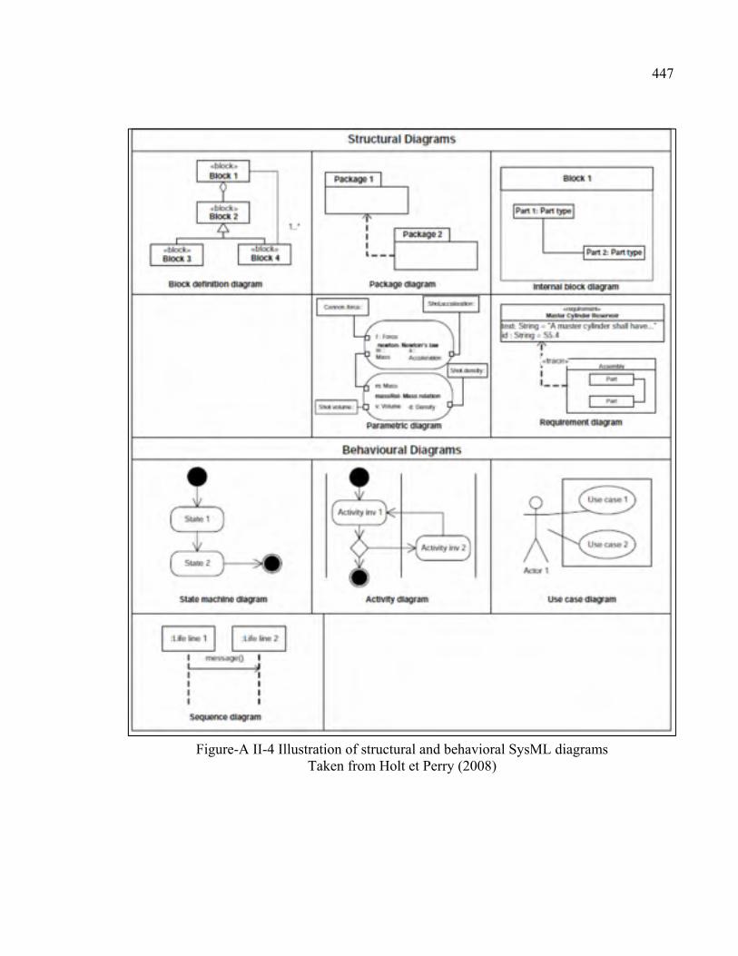
447
Figure-A II-4 Illustration of structural and behavioral SysML diagrams Taken from Holt et Perry (2008)
448
II.4.1 Structural Constructs
This type of constructs defines the static and structural elements typically used in structural
diagrams (i.e., package, block definition, internal block and parametric diagrams).
a. Model elements: are general-purpose constructs to express various types of dependencies
(e.g., import, refine, access, etc.), constraints and comments;
b. Blocks: are the basic structure entities used in SysML. Blocks can be used for either the
logical or the physical decomposition of a system, and can represent software, hardware,
human or any other system element. Each block defines a collection of both structural and
behavioral features to describe the system properties (e.g., properties, operations, etc.);
c. Ports and flows: Ports are interfacing points that an external block uses to connect with
owning block. SysML defines two main types of ports: proxy and full ports. Flows specify
the kinds of items that a block might exchange with its environment;
d. Constraint blocks: is a particular type of blocks that was introduced to allow the integration
of engineering analysis models. It is used to specify constraints (e.g., mathematical
formulas) to which the block properties should conform. Constraint blocks are intended to
be used in multiple contexts.
II.4.2 Behavioral Constructs
This type of constructs defines the dynamic behavioral constructs that are used mainly within
behavioral diagrams (i.e., activity, sequence, state machine, and use case diagrams):
a. Activities: are behavior units commonly attached to a process (can also be defined as
execution units that take time and can be interrupted);
b. Interactions: define constructs for describing message-based interactions between entities;
c. State machines: describe the constructs used to specify state-based behavior (e.g., system
states, transitions between states). A state characterizes the status of a system before
making a transition. A transition is a sequence of actions to be carried out when a condition
is satisfied or when an event takes place;
d. Use cases: describe at high level how the system (i.e., subject) is used by its actors (i.e.,
environment) to achieve a goal or accomplish a mission.
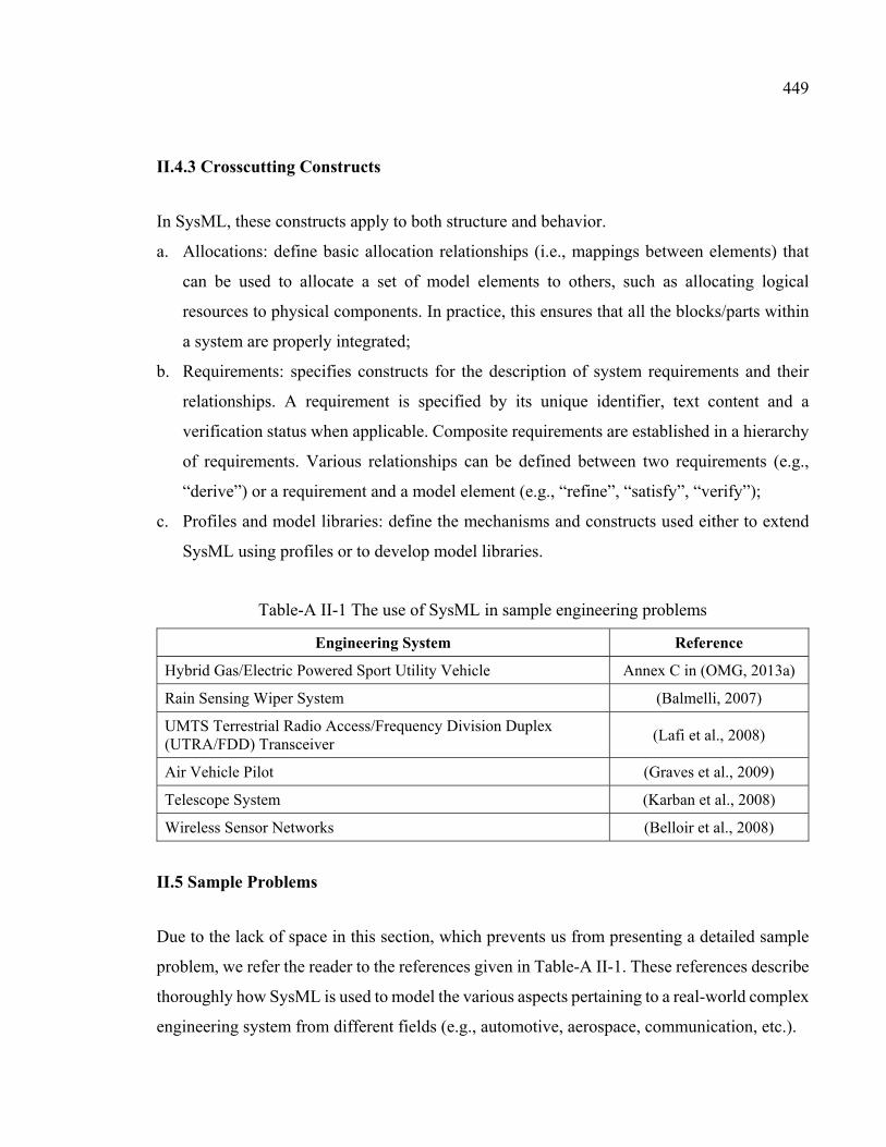
449
II.4.3 Crosscutting Constructs
In SysML, these constructs apply to both structure and behavior.
a. Allocations: define basic allocation relationships (i.e., mappings between elements) that
can be used to allocate a set of model elements to others, such as allocating logical
resources to physical components. In practice, this ensures that all the blocks/parts within
a system are properly integrated;
b. Requirements: specifies constructs for the description of system requirements and their
relationships. A requirement is specified by its unique identifier, text content and a
verification status when applicable. Composite requirements are established in a hierarchy
of requirements. Various relationships can be defined between two requirements (e.g.,
“derive”) or a requirement and a model element (e.g., “refine”, “satisfy”, “verify”);
c. Profiles and model libraries: define the mechanisms and constructs used either to extend
SysML using profiles or to develop model libraries.
Table-A II-1 The use of SysML in sample engineering problems
Engineering System Reference
Hybrid Gas/Electric Powered Sport Utility Vehicle Annex C in (OMG, 2013a)
Rain Sensing Wiper System (Balmelli, 2007)
UMTS Terrestrial Radio Access/Frequency Division Duplex (UTRA/FDD) Transceiver
(Lafi et al., 2008)
Air Vehicle Pilot (Graves et al., 2009)
Telescope System (Karban et al., 2008)
Wireless Sensor Networks (Belloir et al., 2008)
II.5 Sample Problems
Due to the lack of space in this section, which prevents us from presenting a detailed sample
problem, we refer the reader to the references given in Table-A II-1. These references describe
thoroughly how SysML is used to model the various aspects pertaining to a real-world complex
engineering system from different fields (e.g., automotive, aerospace, communication, etc.).

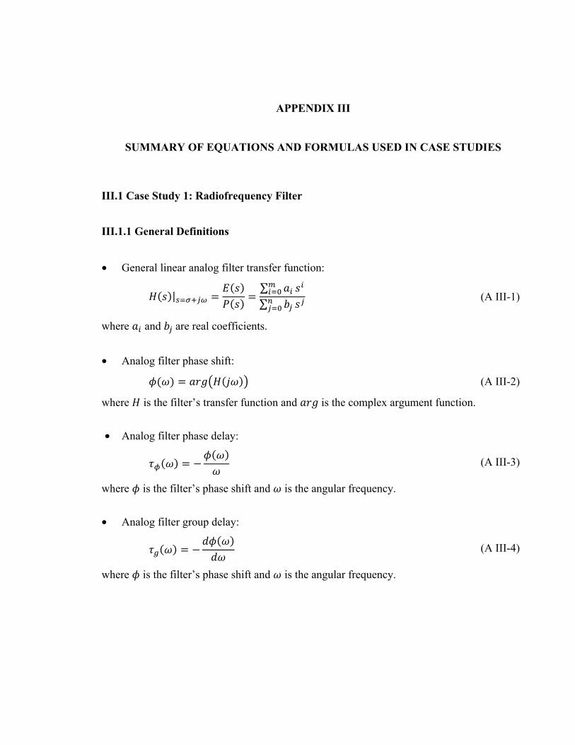
APPENDIX III
SUMMARY OF EQUATIONS AND FORMULAS USED IN CASE STUDIES
III.1 Case Study 1: Radiofrequency Filter
III.1.1 General Definitions
• General linear analog filter transfer function:
( )| = ( )( ) = ∑∑ (A III-1)
where and are real coefficients.
• Analog filter phase shift:
( ) = ( ) (A III-2)
where is the filter’s transfer function and is the complex argument function.
• Analog filter phase delay:
( ) = − ( ) (A III-3)
where is the filter’s phase shift and is the angular frequency.
• Analog filter group delay:
( ) = − ( ) (A III-4)
where is the filter’s phase shift and is the angular frequency.

452
III.1.2 Examples of Filter Approximations
III.1.2.1 Butterworth Filter Approximation
• Butterworth model transfer function:
= | ( )| = 1 + (A III-5)
where is the stopband edge angular frequency and is the filter order.
• Butterworth filter order:
= log 10 − 110 − 12log (A III-6)
where is the maximum attenuation (in dB) in the passband (0 ≤ ≤ ), is the
minimum attenuation (in dB) in the stopband ( ≤ ≤ +∞), is the passband edge angular
frequency and is the stopband edge angular frequency.
• Butterworth lowpass prototype normalized elements:
= = 1= 2 sin (2 − 1)2 , = 1,2, … , (A III-7)
where is the filter order.
III.1.2.2 Chebyshev Type I Filter Approximation
• Chebyshev Type I model transfer function:
= | ( )| = 1 + (A III-8)

453
where is the stopband edge angular frequency, is a measure of the passband ripple and ( ) is the Chebyshev function defined as follows:
( ) = cos[ ∙ cos ( )], 0 ≤ ≤ 1( ) = cosh[ ∙ arccosh( )], > 1 (A III-9)
• Chebyshev Type I filter order:
= arccosh 1 10 − 1arccosh (A III-10)
where is the maximum attenuation (in dB) in the passband (0 ≤ ≤ ), is a measure
of the passband ripple (in dB), is the passband edge angular frequency and is the
stopband edge angular frequency.
• Chebyshev Type I lowpass prototype normalized elements:
= 1= 1,tanh 4 , = 2= 4 , = 2,3, … ,= sin (2 − 1)2 , = 1,2, … ,= + sin , = 1,2, … ,= ln coth 17.32= 10 log( + 1)= sinh 2
(A III-11)
where is the filter order.
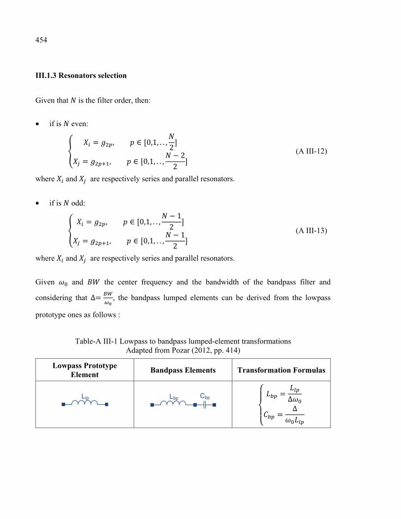
454
III.1.3 Resonators selection
Given that is the filter order, then:
• if is even:
= , ∈ [0,1, . . , 2]= , ∈ [0,1, . . , − 22 ] (A III-12)
where and are respectively series and parallel resonators.
• if is odd:
= , ∈ [0,1, . . , − 12 ]= , ∈ [0,1, . . , − 12 ] (A III-13)
where and are respectively series and parallel resonators.
Given and the center frequency and the bandwidth of the bandpass filter and
considering that ∆= , the bandpass lumped elements can be derived from the lowpass
prototype ones as follows :
Table-A III-1 Lowpass to bandpass lumped-element transformations Adapted from Pozar (2012, pp. 414)
Lowpass Prototype Element
Bandpass Elements Transformation Formulas
Llp
CbpLbp
= ∆= ∆
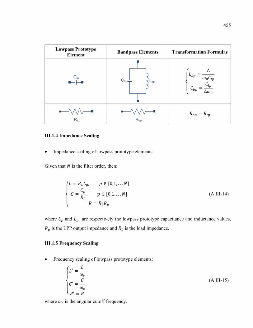
455
Lowpass Prototype Element
Bandpass Elements Transformation Formulas
Clp
LbpCbp
= ∆= ∆
Rlp Rbp
=
III.1.4 Impedance Scaling
• Impedance scaling of lowpass prototype elements:
Given that is the filter order, then:
= , ∈ [0,1, . . , ]= , ∈ [0,1, . . , ]= (A III-14)
where and are respectively the lowpass prototype capacitance and inductance values,
is the LPP output impedance and is the load impedance.
III.1.5 Frequency Scaling
• Frequency scaling of lowpass prototype elements:
′ =′ =′ = (A III-15)
where is the angular cutoff frequency.
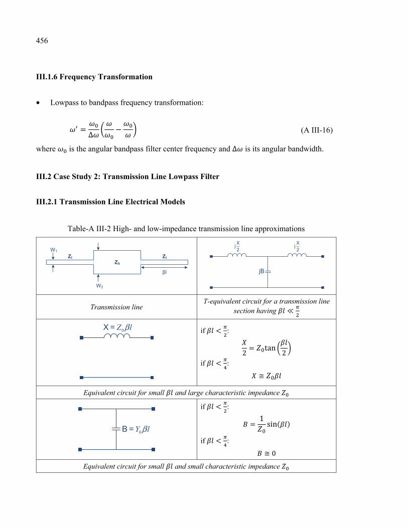
456
III.1.6 Frequency Transformation
• Lowpass to bandpass frequency transformation:
= ∆ − (A III-16)
where is the angular bandpass filter center frequency and ∆ is its angular bandwidth.
III.2 Case Study 2: Transmission Line Lowpass Filter
III.2.1 Transmission Line Electrical Models
Table-A III-2 High- and low-impedance transmission line approximations
W2
βl
W1
Zh
Zl Zl
jB
Xj2
Xj2
Transmission line T-equivalent circuit for a transmission line
section having ≪
0Z lβX =
if < :
2 = 0tan 2
if < : ≅ 0
Equivalent circuit for small and large characteristic impedance
0Y lβB =
if < : = 10 sin( ) if < : ≅ 0
Equivalent circuit for small and small characteristic impedance
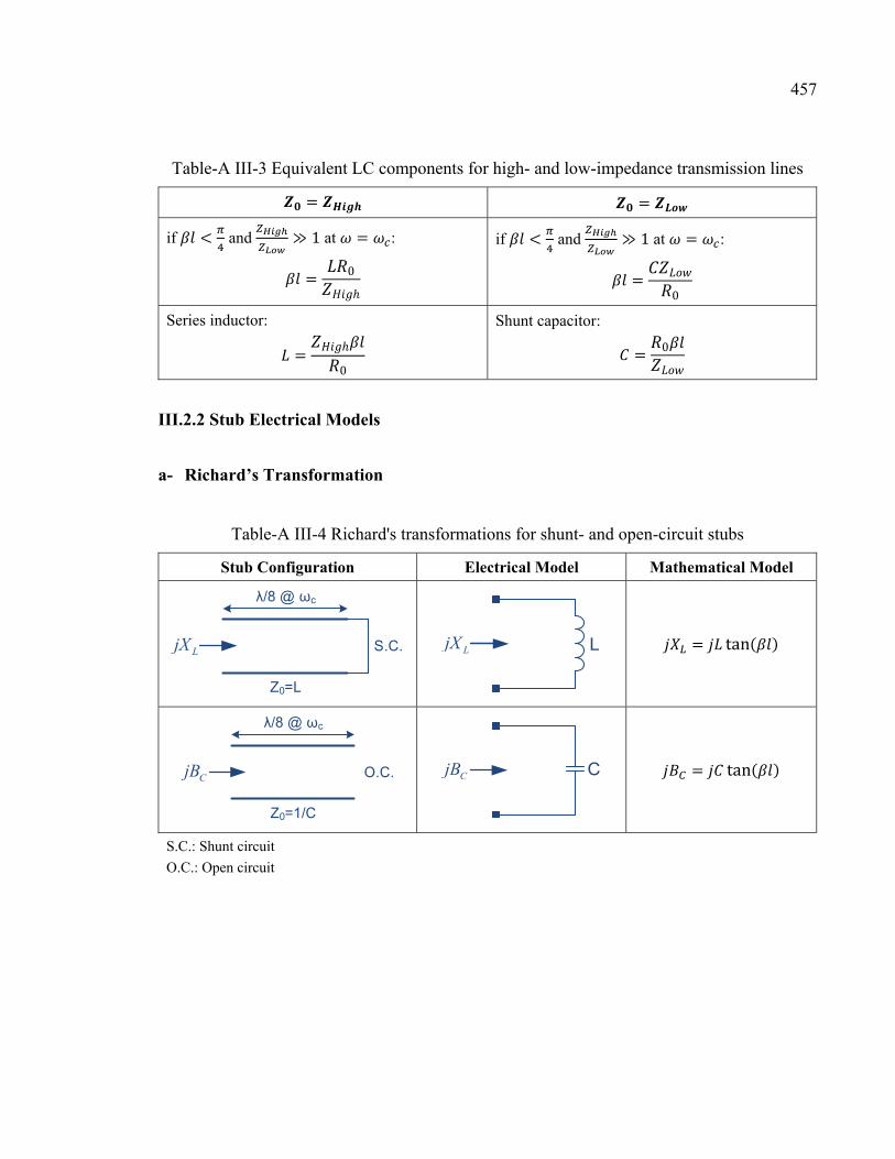
457
Table-A III-3 Equivalent LC components for high- and low-impedance transmission lines = =
if < and ≫ 1 at = : = 0ℎ
if < and ≫ 1 at = : = 0
Series inductor: = ℎ0
Shunt capacitor: = 0
III.2.2 Stub Electrical Models
a- Richard’s Transformation
Table-A III-4 Richard's transformations for shunt- and open-circuit stubs
Stub Configuration Electrical Model Mathematical Model
S.C.
λ/8 @ ωc
Z0=L
LjX LLjX
= tan( )
O.C.
λ/8 @ ωc
Z0=1/C
CjB
CCjB
= tan( ) S.C.: Shunt circuit
O.C.: Open circuit
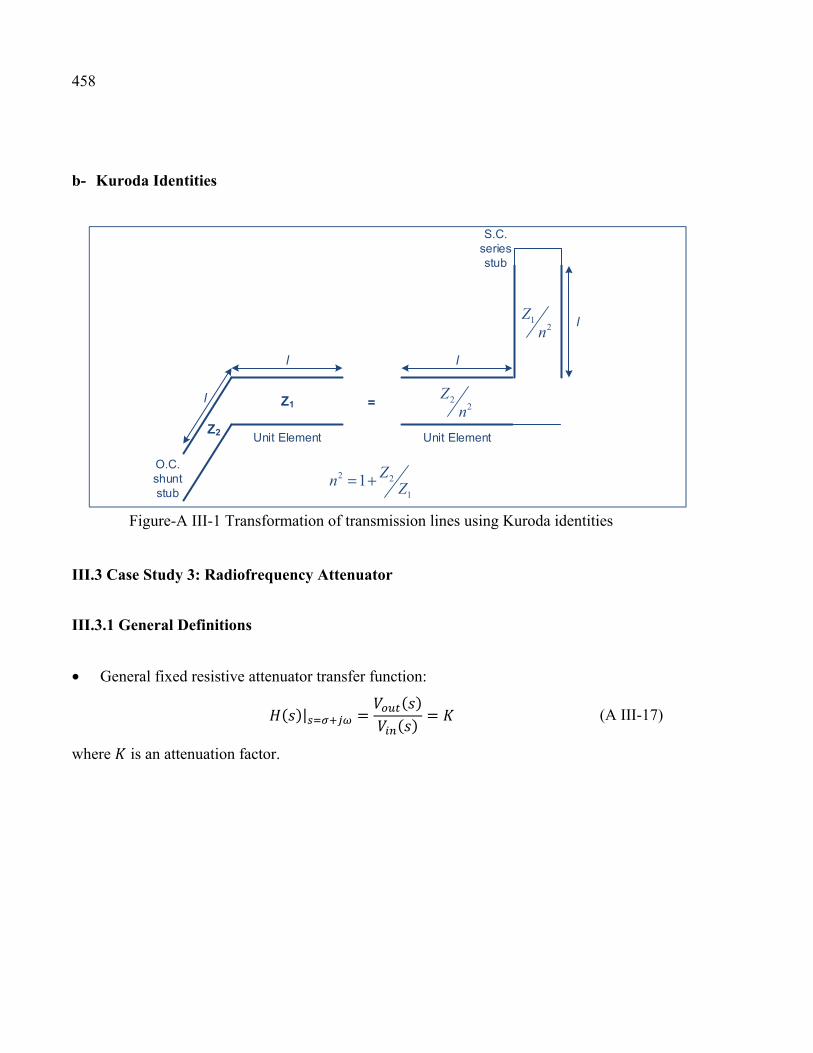
458
b- Kuroda Identities
O.C.shunt stub
l
Z1 22
Zn
l
Unit ElementZ2
=
l
Unit Element
S.C. series stub
12
Zn
2 2
11 Zn Z= +
l
Figure-A III-1 Transformation of transmission lines using Kuroda identities
III.3 Case Study 3: Radiofrequency Attenuator
III.3.1 General Definitions
• General fixed resistive attenuator transfer function:
( )| = ( )( ) = (A III-17)
where is an attenuation factor.
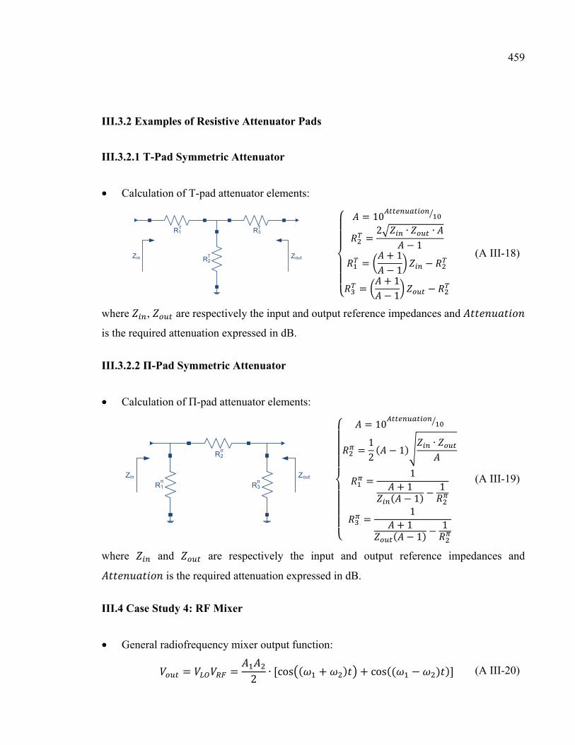
459
III.3.2 Examples of Resistive Attenuator Pads
III.3.2.1 T-Pad Symmetric Attenuator
• Calculation of T-pad attenuator elements:
R2
R1 R3
ZoutZin
T
T
T
= 10= 2 ∙ ∙− 1= + 1− 1 −= + 1− 1 − (A III-18)
where , are respectively the input and output reference impedances and
is the required attenuation expressed in dB.
III.3.2.2 Π-Pad Symmetric Attenuator
• Calculation of Π-pad attenuator elements:
R1 R3
R2
Zin Zoutπ
π
π
= 10= 12 ( − 1) ∙= 1+ 1( − 1) − 1= 1+ 1( − 1) − 1
(A III-19)
where and are respectively the input and output reference impedances and
is the required attenuation expressed in dB.
III.4 Case Study 4: RF Mixer
• General radiofrequency mixer output function:
= = 2 ∙ [cos ( + ) + cos(( − ) )] (A III-20)
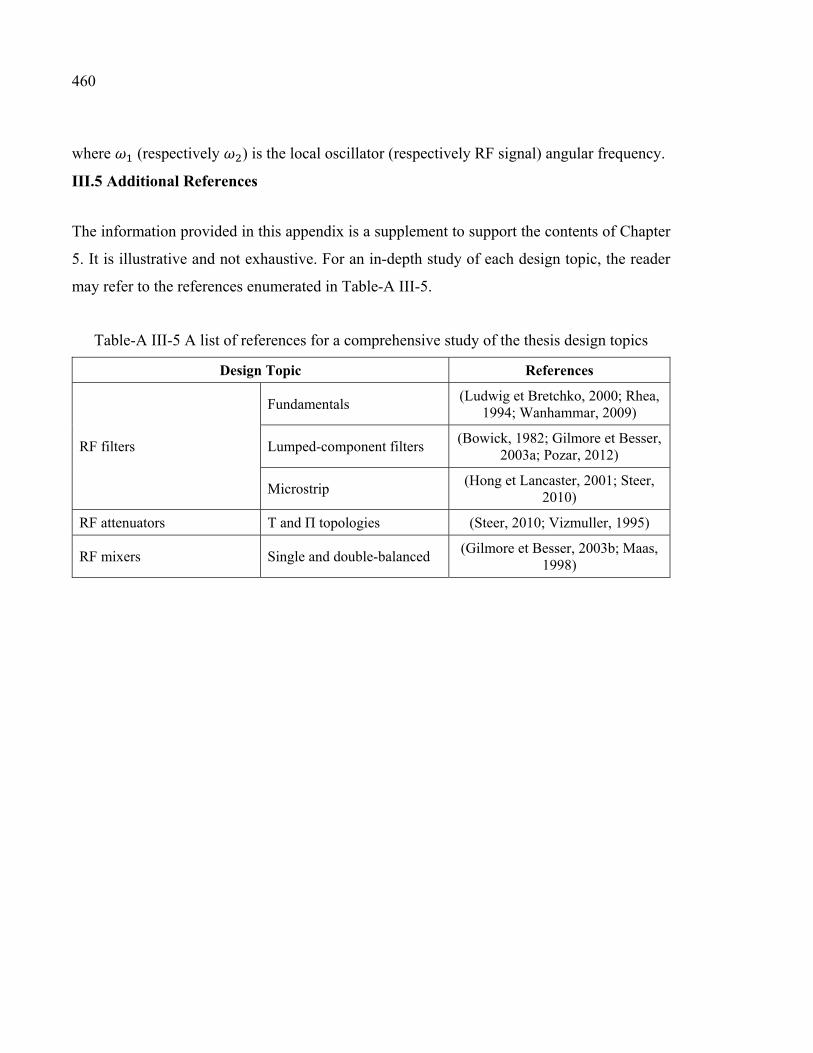
460
where (respectively ) is the local oscillator (respectively RF signal) angular frequency.
III.5 Additional References
The information provided in this appendix is a supplement to support the contents of Chapter
5. It is illustrative and not exhaustive. For an in-depth study of each design topic, the reader
may refer to the references enumerated in Table-A III-5.
Table-A III-5 A list of references for a comprehensive study of the thesis design topics
Design Topic References
RF filters
Fundamentals (Ludwig et Bretchko, 2000; Rhea,
1994; Wanhammar, 2009)
Lumped-component filters (Bowick, 1982; Gilmore et Besser,
2003a; Pozar, 2012)
Microstrip (Hong et Lancaster, 2001; Steer,
2010)
RF attenuators T and Π topologies (Steer, 2010; Vizmuller, 1995)
RF mixers Single and double-balanced (Gilmore et Besser, 2003b; Maas,
1998)
461
LIST OF REFERENCES
Abelson, Harold, Gerald Jay Sussman et Julie Sussman. 1996. Structure and Interpretation of Computer Programs, Second. MIT Press.
Agilent. 2005. « Using Circuit Simulators »
< http://cp.literature.agilent.com/litweb/pdf/ads2005a/pdf/cktsim.pdf >. Agilent. 2010a. « Exporting Files Using Genesys ».
<http://edocs.soco.agilent.com/display/genesys2010/Exporting+Data+Files+Using+Genesys >. Consulté le 17 April 2014.
Agilent. 2010b. « Importing Data Files Using SystemVue ».
<http://edocs.soco.agilent.com/display/sv201007/Importing+Data+Files+Using+SystemVue#ImportingDataFilesUsingSystemVue-XMLFileImport >. Consulté le 17 April 2014.
Agilent Technologies, Inc. 2008. « ADS Ptolemy Simulation ».
< http://cp.literature.agilent.com/litweb/pdf/ads2008/pdf/ptolemy.pdf >. Agilent Technologies, Inc. 2013. « Agilent EEsof EDA: Product Overview ».
< http://literature.cdn.keysight.com/litweb/pdf/5991-3154EN.pdf?cmpid=zzfindeesof-catalog >. Consulté le 5 September 2013.
Aguayo Gonzalez, Carlos R., Francisco M. Portelinha et Jeffery H. Reed. 2007. « Part 1:
Design and Implementation of an SCA Core Framework for a DSP Platform ». Military Embedded Systems Magazine.
Akretch, Faride. 2012. « Where RF meets analog and digital—the new embedded reality ».
<http://www.edn.com/electronics-blogs/scope-guru-on-signal-integrity/4395965/Where-RF-meets-analog-and-digital-the-new-embedded-reality >. Consulté le January 2014.
Allen, Phillip E., et Douglas R. Holberg. 2002. CMOS Analog Circuit Design, Second Oxford
University Press. Almeida, Pedro De. 2008. « Model-Driven Architecture – Improving Software Development
in Large-Scale Enterprise Applications ». University of Fribourg, Switzerland. Anderson, David L. 2009. « An evaluation of current and future costs for lithium-ion batteries
for use in electrified vehicle powertrains ». Duke University. Andrew, Rufus. 2011. « 2020: The Ubiquitous Heterogeneous Network - Beyond 4G ».
< http://www.itu.int/dms_pub/itu-t/oth/29/05/T29050000130001PDFE.pdf >.
462
Andriana Voulkidou, Stylianos Siskos et Thomas Noulis. 2012. « Simulation Inaccuracies in Analog/RF Integrated Circuit Design in CMOS Process ». In Second Pan-Hellenic Conference on Electronics and Telecommunications.
Arabi, Eyad, et Sadiq Ali. 2008. « Behavioral Modeling of RF front end devices in Simulink
». Chalmers University of Technology, Sweden. Archer, Norman P, Milena M Head et Yufei Yuan. 1996. « Patterns in information search for
decision making: the effects of information abstraction ». International Journal of Human-Computer Studies, vol. 45, no 5, p. 599-616.
Ashbaugh, Floyd. 2009. « Meeting the Challenges of RF Wireless Design ».
<http://www.electronicproducts.com/Analog_Mixed_Signal_ICs/Sensors/Meeting_the_challenges_of_RF_wireless_design.aspx >. Consulté le 5 January 2014.
Bahl, Inder Jit. 2003. Lumped elements for RF and microwave circuits. Artech house. Bako, Niko, Zeljko Butkovic et Adrijan Baric. 2010. « Design of Fully Differential Folded
Cascode Operational Amplifier by the gm/ID Methodology ». In Proceedings of the 33rd International Convention. (Opatija, 24-28 May 2010 ), p. 89-94. IEEE.
Baldwin, Douglas, et Greg W. Scragg. 2004. The Object Primer. Cambridge University Press. Balkir, Sina, Günhan Dündar et A Selcuk Ögrenci. 2003. Analog VLSI Design Automation.
CRC Press. Balmelli, Laurent. 2007. « An Overview of the Systems Modeling Language for Products and
Systems Development ». Journal of Object Technology, vol. 6, no 6. Baudry, Benoit, Clementine Nebut et Yves Le Traon. 2007. « Model-driven engineering for
requirements analysis ». In Enterprise Distributed Object Computing Conference, 2007. EDOC 2007. 11th IEEE International. p. 459-459. IEEE.
Belloir, Nicolas, Jean-Michel Bruel, Natacha Hoang et Congduc Pham. 2008. « Utilisation de
SysML pour la modélisation des réseaux de capteurs ». In 14éme Colloque International sur les Langages et Modèles à Objets. (Montréal), p. 169-184.
Berkley Design Automation. 2009. « Big Analog/RF Automation: Complex-Block
Characterization and Full-Circuit Performance Simulation ». Beydeda, Sami, Matthias Book et Volker Gruhn. 2005. Model-driven software development,
15. Springer. Bézivin, Jean. 2005. « On the unification power of models ». Software & Systems Modeling,
vol. 4, no 2, p. 171-188.
463
Bizzarri, Federico, Angelo Brambilla et Giancarlo Storti Gajani. 2011. « Phase Noise Simulation in Analog Mixed Signal Circuits: An Application to Pulse Energy Oscillators ». Ieee Transactions on Circuits and Systems Ii-Express Briefs, vol. 58, no 3, p. 154-158.
Blackburn, Mark R. 2008. What’s Model Driven Engineering (MDE) and how can it impact
process, people, tools and productivity. Tech. Rep. Systems and Software Consortium, Inc.
Blyler, John. 2006. « Analog-RF IP Integration Challenges SoC Designers ». Chip Design
Magazine. < http://chipdesignmag.com/display.php?articleId=435 >. Consulté le 26 February 2014.
Bowick, Chris 1982. RF Circuit Design. Newnes. Brambilla, Marco, Jordi Cabot et Manuel Wimmer. 2012. « Model-driven software
engineering in practice ». Synthesis Lectures on Software Engineering, vol. 1, no 1, p. 1-182.
Briand, Lionel, Williams, Clay. 2005. « Model Driven Engineering Languages and Systems ».
In 8th International Conference, MoDELS 2005. (Montego Bay, Jamaica), p. October 2-7, 2005.
Briggs, Mark. 2010. « Dynamic Frequency Selection (DFS) and the 5-GHz Unlicensed
Band ». Cadence Design Systems, Inc. 2002. « The Rise of Digital/Mixed-signal Semiconductors and
Systems-on-a-Chip ». « Cadence Design Tools Tutorial ». 2010.
< http://lsmwww.epfl.ch/Education/CadenceTutorial/flow.html >. Consulté le 1 September 2013.
Cardinal, Mario. 2013. Executable Specifications with Scrum: A Practical Guide to Agile
Requirements Discovery. Addison-Wesley. Chang, Henry, et Ken Kundert. 2007. « Verification of complex analog and RF IC designs ».
Proceedings of the IEEE, vol. 95, no 3, p. 622-639. Chapin, John, et William Lehr. 2011. « Mobile broadband growth, spectrum scarcity, and
sustainable competition ». In. TPRC. Chen, Deming. 2009a. « Design automation for microelectronics ». In Springer Handbook of
Automation. p. 653-670. Springer.
464
Chen, Deming. 2009b. « Springer Handbook of Automation ». In Design Automation for Microelectronics, sous la dir. de Nof, Shimon Y., p. 653-667. Springer.
Chen, Lijun J., Steven H. Low et John C. Doyle. 2011. « Cross-layer design in multihop
wireless networks ». Computer Networks, vol. 55, no 2, p. 480-496. Cheng, Qingsha S., John W. Bandler, Slawomir Koziel, Mohamed H. Bakr et Stanislav
Ogurtsov. 2010. « The state of the art of microwave CAD: EM-based optimization and modeling ». International Journal of RF and Microwave Computer-Aided Engineering, vol. 20, no 5, p. 475-491.
Chia, Stanley, Trevor Gill, L. Ibbetson, D. Lister, A. Pollard, R. Irmer, D. Almodovar, N.
Holmes et S. Pike. 2008. « 3G evolution ». Ieee Microwave Magazine, vol. 9, no 4, p. 52-63.
Chien, Andrew A., et Vijay Karamcheti. 2013. « Moore's Law: The first ending and a new
beginning ». Computer, no 12, p. 48-53. Chonoles, Michael Jesse, et James A Schardt. 2011. UML 2 for Dummies. John Wiley & Sons. CIC. 2003. « Mixed-Signal IC Design Kit Training Manual ». p. 157. < http://www2.ece.ohio-
state.edu/~bibyk/ece822/MSDK_July_2003.pdf >. Consulté le 6 May 2014. Cisco. 2013. « Cisco Visual Networking Index: Global Mobile Data Traffic Forecast 2012–
2017 ». <http://www.cisco.com/en/US/solutions/collateral/ns341/ns525/ns537/ns705/ns827/VNI-Forecast_QA.pdf >. Consulté le 22 March 2013.
Cisco. 2015. « Cisco Visual Networking Index: Global Mobile Data Traffic Forecast Update,
2014–2019 ». < http://www.cisco.com/c/en/us/solutions/collateral/service-provider/visual-networking-index-vni/white_paper_c11-520862.pdf >. Consulté le 15 July 2015.
Comer, David J. 1985. « A theoretical basis for practical amplifier design using cascaded
operational amplifiers ». In IEE Proceedings G (Electronic Circuits and Systems). Vol. 132, p. 161-164. IET.
Cornell University, Lectures. 2011. « Modular Programming: Modules and Signatures ».
<https://www.cs.cornell.edu/courses/cs3110/2011sp/lectures/lec07-modules/modules.htm >. Consulté le 19 May 2014.
Costa-Perez, Xavier, Andreas Festag, Hans-Joerg Kolbe, Juergen Quittek, Stefan Schmid,
Martin Stiemerling, Joerg Swetina et Hans van der Veen. 2013. « Latest Trends in Telecommunication Standards ». Acm Sigcomm Computer Communication Review, vol. 43, no 2, p. 64-71.
465
Dackenberg, Jens. 2010. « Software Communication Architecture-Waveform Distribution with MHAL ».
David, Alexandre, et Brian Nielsen. 2008. « Model-Driven Development of Embedded Real-
Time Systems ». ERCIM News, vol. 2008, no 75. De Smedt, Bart, et Georges Gielen. 1999. « Models for systematic design and verification of
frequency synthesizers ». Circuits and Systems II: Analog and Digital Signal Processing, IEEE Transactions on, vol. 46, no 10, p. 1301-1308.
Delligatti, Lenny (304). 2013. SysML Distilled: A Brief Guide to the Systems Modeling
Language, First. Addison-Wesley Professional. Dewey, Allen. 2000. « Digital and Analog Electronic Design Automation ». In The Electrical
Engineering Handbook, sous la dir. de Dorf, Richard C.: CRC Press LLC. Dunham, William, Rich Kirkham, Doug Stolarz et Juergen Hartung. 2003. « RF Module
Design: Requirements and Issues ». RF Design Magazine. Dutton, Robert W. 1997. « Device Simulation for RF Applications ». In International Electron
Devices Meeting Technical Digest. p. 301-304. El-Khatib, Ziad, Leonard MacEachern et Samy A Mahmoud. 2012. Distributed CMOS
Bidirectional Amplifiers: Broadbanding and Linearization Techniques. Springer Science & Business Media.
Embley, David W., et Bernhard Thalheim. 2011. Handbook of Conceptual Modeling: Theory,
Practice, and Research Challenges. Springer. Fernandes, João. « Principles of Model-Driven Software Engineering ». no 6 June 2014, p. 49.
< http://alba.di.uminho.pt/por/content/download/2667/14015/file/unit7-mdse.pdf >. Ferragina, Vincenzo, Nicola Ghittori, Guide Torelli, Giorgio Boselli, Gabriella Trucco et
Valentino Liberali. 2005. « Analysis of Crosstalk Effects on Mixed-Signal CMOS ICs with Different Mounting Technologies ». In Instrumentation and Measurement Technology Conference, 2005. IMTC 2005. Proceedings of the IEEE. Vol. 3, p. 1979-1984. IEEE.
Foster, Harry. 2012. « The 2012 Wilson Research Group Functional Verification Study ».
<http://www.mentor.com/products/fv/multimedia/the-2012-wilson-research-group-functional-verification-studyview >. Consulté le June 3, 2013.
Fowler, Martin. 2004. UML distilled: a brief guide to the standard object modeling language.
Addison-Wesley Professional.
466
Frankel, David S. 2003. Model Driven Architecture: Applying MDA to Enterprise Computing. John Wiley and Sons.
Frevert, Ronny, Joachim Haase, Roland Jancke, Uwe Knochel, Peter Schwarz, Ralf Kakerow
et Mohsen Darianian. 2006. Modeling and Simulation for RF System Design. Springer Science & Business Media.
Friedenthal, Sanford, Alan Moore et Rick Steiner. 2008. A Practical Guide to SysML: The
Systems Modeling Language. Morgan Kaufmann. Gajski, Daniel D., et Robert H. Kuhn. 1983. « New VLSI Tools ». Computer. Vol. 16, no 12,
p. 11-14. Gajski, Daniel D., Frank Vahid et Sanjiv Narayan. 1994. « A System-Design Methodology:
Executable-Specification Refinement ». In The European Conference on Design Automation. (Paris, 28 Feb-3 Mar 1994 ), p. 458-463. IEEE. <http://ieeexplore.ieee.org/ielx2/946/7755/00326836.pdf?tp=&arnumber=326836&isnumber=7755 >.
Gerez, Sabih H. 1999. Algorithms for VLSI design automation, 8. Wiley New York. Gianesello, Fred. 2012. « Analog and RF Requirements for Advanced CMOS Nodes: The SOI
Perspective ». In Lund Circuit Design Workshop. (October 3, 2012). < http://cdworkshop.eit.lth.se/fileadmin/eit/group/71/2012/STM-Gianesello.pdf >.
Gielen, Georges G.E., et Rob A. Rutenbar. 2000. « Computer-Aided Design of Analog and
Mixed-Signal Integrated Circuits ». In IEEE Proceedings. Vol. 88, p. 1825-1852. <http://ieeexplore.ieee.org/ielx5/5/19471/00899053.pdf?tp=&arnumber=899053&isnumber=19471 >.
Gielen, Georges G.E. 2007. « Design tool solutions for mixed-signal/RF circuit design in
CMOS nanometer technologies ». In Proceedings of the 2007 Asia and South Pacific Design Automation Conference. p. 432-437. IEEE Computer Society.
Gilmore, Rowan, et Less Besser. 2003a. Practical RF Circuit Design for Modern Wireless
Systems: Volume I – Passive Circuits and Systems. Artech House. Gilmore, Rowan, et Less Besser. 2003b. Practical RF Circuit Design for Modern Wireless
Systems: Volume II – Active Circuits and Systems. Artech House. Goldstone, Robert L., et Lawrence W. Barsalou. 1998. « Reuniting perception and
conception ». Cognition, vol. 65, no 2, p. 231-262.
467
González, Delia Rodríguez de Llera, Ana Rusu et Mohammed Ismail. 2007. « EDA for RF and analog front-ends in the 4G Era: Challenges and solutions ». In Circuit Theory and Design, 2007. ECCTD 2007. 18th European Conference on. p. 24-27. IEEE.
Grant, Doug. 2012. « RF, meet Analog; and his friend Digital ».
< http://www.eetimes.com/author.asp?section_id=36&doc_id=1285742 >. Consulté le 26 February 2014.
Graves, Henson, Stephen Guest, Jeff Vermette et Yvonne Bijan. 2009. « Air Vehicle Model-
Based Design and Simulation Pilot ». In Simulation Interoperability Workshop (SIW). <http://www.omgwiki.org/MBSE/lib/exe/fetch.php?media=mbse:09s-siw-056_mbds.pdf >.
Green, Leslie. 2001. « RF-inductor Modeling for the 21st Century ». EDN Magazine, vol. 46,
no 22, p. 67-74. Grout, Ian. 2008. Digital Systems Design with FPGAs and CPLDs. Newnes. Gruner, Daniel, Zihui Zhang, Viswanathan Subramanian, Falk Korndoerfer et Georg Boeck.
2007. « Lumped Element MIM capacitor model for Si-RFICs ». In Microwave and Optoelectronics Conference, 2007. IMOC 2007. SBMO/IEEE MTT-S International. p. 149-152. IEEE.
Guo, Weisi OFarrell, Tim. 2011. « Reducing Energy Consumption of Wireless
Communications ». In United Kingdom Council Conference on Digital Engagement. Handziski, Vlado, Joseph Polastre, Jan-Hinrich Hauer, Cory Sharp, Adam Wolisz et David
Culler. 2005. « Flexible hardware abstraction for wireless sensor networks ». In Wireless Sensor Networks, 2005. Proceeedings of the Second European Workshop on. p. 145-157. IEEE.
Hansen, K. 2003. « Wireless RF design challenges ». 2003 Ieee Radio Frequency Integrated
Circuits (Rfic) Symposium, Digest of Papers, p. 3-7. Hartin, OL, et Evan Yu. 2006. « RF Physical Device Simulation for Wireless Applications ».
In 2006 16th Biennial University/Government/Industry Microelectronics Symposium. Henke, Russ. 2010a. « Agilent EEsof EDA – Part I ».
<http://www10.edacafe.com/nbc/articles/view_weekly.php?section=Magazine&articleid=782353 >. Consulté le 5 January 2013.
Henke, Russ. 2010b. « Agilent EEsof EDA – Part II ».
<http://www10.edacafe.com/nbc/articles/view_article.php?articleid=803282&page_no=1 >. Consulté le 5 January 2013.
468
Henry, Sallie M, et Mark Lattanzi. 1994. « Measurement of Software Maintainability and Reusability in the Object Oriented Paradigm ».
Holt, Jon, et Simon Perry. 2008. SysML for Systems Engineering. The Institution of
Engineering and Technology. Hong, Jia-Sheng, et M.J. Lancaster. 2001. Microstrip Filters for RF/Microwave Applications.
John Wiley and Sons. Hsiung, Pao-Ann, Shang-Wei Lin, Yean-Ru Chen, Nien-Lin Hsueh, Chih-Hung Chang, Chih-
Hsiong Shih, Chorng-Shiuh Koong, Chao-Sheng Lin, Chun-Hsien Lu et Sheng-Ya Tong. 2009. « Model-driven development of multi-core embedded software ». In Multicore Software Engineering, 2009. IWMSE'09. ICSE Workshop on. p. 9-16. IEEE.
Hu, Chenming. 1993. « Future CMOS scaling and reliability ». Proceedings of the IEEE, vol.
81, no 5, p. 682-689. Hubbard, Mathew 2012. « Taming the Smartphone Power Consumption Vicious Cycle ».
Microwave Journal, vol. 55, no 11, p. 92-96. InetDaemon.Com. 2013. « A Comparison of Network Models ».
<http://www.inetdaemon.com/tutorials/basic_concepts/network_models/comparison.shtml >. Consulté le 28 April 2013.
Iniewski, Krzysztof. 2007. Wireless technologies: circuits, systems, and devices. CRC press. Intel. 2013a. « Intel Chips Timeline ».
<http://www.intel.com/content/www/us/en/history/history-intel-chips-timeline-poster.html >.
Intel. 2013b. « Transistors to Transformations: From Sand to Circuits - How Intel Makes
Chips ». < http://exploreintel.com/assets/pdf/aloha/museum-transistors-to-transformations-brochure.pdf >.
Irmer, R., et S. Chia. 2009. « Signal Processing Challenges for Future Wireless
Communications ». 2009 Ieee International Conference on Acoustics, Speech, and Signal Processing, Vols 1- 8, Proceedings, p. 3625-3628.
ITU. 2013. « Trends in Telecommunication Reform 2013: Transnational Aspects of Regulation
in a Networked Society ». < http://www.itu.int/dms_pub/itu-d/opb/reg/D-REG-TTR.14-2013-SUM-PDF-E.pdf >. Consulté le 30 may 2013.
Jiang, Hai, Weihua H. Zhuang et Xuemin M. Shen. 2005. « Cross-layer design for resource
allocation in 3G wireless networks and beyond ». Ieee Communications Magazine, vol. 43, no 12, p. 120-126.
469
JTRS. 2010. Joint Tactical Radio System (JTRS) Standard Modem Hardware Abstraction Layer Application Program Interface (API). Joint Program Executive Office. < http://jtnc.mil/sca/Documents/SCA_APIs/API_3.0_20131002_Mhal.pdf >.
Kao, Chia-Hsiung, Yin-Fang Wei et Huan-Chou Kuo. 2001. « A rail-to-rail CMOS operational
amplifier design for low voltage systems ». Proc. AMPC, vol. 1, p. 276-279. Karban, Robert, Michele Zamparelli, Bertrand Bauvir, Bertrand Koehler, Lothar Noethe et A.
Balestra. 2008. « Exploring Model Based Engineering for Large Telescopes - Getting Started with Descriptive Models ». SPIE Astronomical Telescopes and Instrumentation.
Kelly, Steven, et Juha-Pekka Tolvanen. 2008. Domain-Specific Modeling: Enabling Full Code
Generation. John Wiley and Sons. Kendal, Simon. 2011. Object Oriented Programming Using C#. Simon Kendal & Ventus
Publishing. Kevenaar, Tom A.M., et E.J.W. ter Maten. 1999. « RF IC Simulation: State-of-the-art and
Future Trends ». In International Conference on Simulation of Semiconductor Processes and Devices. (Kyoto, 06 Sep 1999-08 Sep 1999 ), p. 7-10. <http://ieeexplore.ieee.org/ielx5/6469/17293/00799246.pdf?tp=&arnumber=799246&isnumber=17293 >.
Khare, Kavita, Nilay Khare et Pawan Kumar Sethiya. 2008. « Analysis of low voltage rail-to-
rail CMOS operational amplifier design ». In Electronic Design, 2008. ICED 2008. International Conference on. p. 1-4. IEEE.
Kienhuis, Bart, Ed Deprettere, Kees Vissers, Pieter Van der Wolf, Paul Lieverse et Edward
Lee. 2000. « Y-chart Methodology and Models of Computation and Architecture ». In 37th Design Automation Conference.
Kleppe, Anneke G., Jos Warmer et Wim Bast. 2003. MDA Explained - The Model-driven
Architecture: Practice and Promise. Addison-Wesley Longman Publishing Co., Inc., Boston, MA.
Klump, Raymond P. 2001. « Understanding Object-Oriented Programming Concepts ». In
IEEE Power Engineering Society Summer Meeting. (Vancouver, 15 Jul 2001-19 Jul 2001 ). Vol. 2, p. 1070-1074. <http://ieeexplore.ieee.org/ielx5/7659/20923/00970207.pdf?tp=&arnumber=970207&isnumber=20923 >.
Koffman, Elliot B., et Paul A.T. Wolfgang. 2006. Objects, Abstraction, Data Structures and
Design Using C++. John Wiley and Sons.
470
Korhonen, Kaisa. 2011. « Predicting Mobile Device Battery Life ». Aalto University, Finland. Koutitas, George, et Panagiotis Demestichas. 2010. « A review of energy efficiency in
telecommunication networks ». Telfor journal, vol. 2, no 1, p. 2-7. Kundert, Ken, et Henry Chang. 2005. « Top-Down Design and Verification of Mixed-Signal
Integrated Circuits ». p. 1-8. Kundert, Ken, Henry Chang, David Jefferies, G. Lamant, Enrico Malavasi et F. Sendig. 2000.
« Design of mixed-signal systems-on-a-chip ». Ieee Transactions on Computer-Aided Design of Integrated Circuits and Systems, vol. 19, no 12, p. 1561-1571.
Kundert, Ken. 2005. « Challenges in RF Simulation ». In RF IC Symposium. Kundert, Ken. 2006. « Principles of Top-Down Mixed-Signal Design ». p. 1-31. Lafi, Sabeur, Roger Champagne, Ammar B. Kouki et Jean Belzile. 2008. « Modeling radio-
frequency front-ends using sysml: A case study of a umts transceiver ». ACESMB 2008, p. 115.
Lang Tong, et al. 2002. « Future Challenges of Signal Processing and Communications in
Wireless Networks ». In NSF/ONR/ARL Workshop on Future Directions in Signal Processing and Wireless Networking.
Lange, Christoph, Dirk Kosiankowski, A. Betker, H. Simon, Nico Bayer, Dirk von Hugo, H.
Lehmann et Andreas Gladisch. 2014. « Energy Efficiency of Load-Adaptively Operated Telecommunication Networks ». Journal of Lightwave Technology, vol. 32, no 4, p. 571-590.
Lange, Christian F.J., Michel R.V. Chaudron et Johan Muskens. 2006. « In practice: UML
software architecture and design description ». Software, IEEE, vol. 23, no 2, p. 40-46. Lavagno, Luciano, Grant Martin et Louis Scheffer. 2006. Electronic Design Automation for
Integrated Circuits Handbook-2 Volume Set. CRC Press, Inc. Lee, Young, et Kai H Chang. 2000. « Reusability and maintainability metrics for object-
oriented software ». In Proceedings of the 38th annual on Southeast regional conference. p. 88-94. ACM.
Leenaerts, Domine; Georges G.E. ; Gielen et Rob A. Rutenbar. 2001. « CAD Solutions and
Outstanding Challenges for Mixed-Signal and RF IC Design ». In IEEE/ACM International Conference on Computer-Aided Design. (4-8 Nov. 2001 ), p. 270-277. <http://ieeexplore.ieee.org/ielx5/7652/20895/00968633.pdf?tp=&arnumber=968633&isnumber=20895 >.
471
Li, Xin, B. Taylor, Yu Tsun Chien et Lawrence T. Pileggi. 2007. « Adaptive post-silicon tuning for analog circuits: Concept, analysis and optimization ». Ieee/Acm International Conference on Computer-Aided Design Digest of Technical Papers, Vols 1 and 2, p. 450-457.
Lidow, Alex, et Strydom, Johan. 2013. « GaN Transistors for Efficient Power Conversion ».
Power Electronics Europe Magazine, no 3, p. 38-40. Lin, Jin, et Zhao Tong. 2011. « EDA Technology and its Implementation in Modern Electronic
Technology ». In International Conference on Business Management and Electronic Information. (Guangzhou, 13-15 May 2011 ). Vol. 2, p. 816-819. IEEE. <http://ieeexplore.ieee.org/ielx5/5871804/5917827/05920355.pdf?tp=&arnumber=5920355&isnumber=5917827 >.
Lin, Rung-Bin. 2005. « Electronic Design Automation: Evolution, Education and
Profession ». <http://vlsi.cse.yzu.edu.tw/%E6%96%87%E7%AB%A0/Electronic%20Design%20Automation.pdf >.
Lind, Gregg, et Cameron Littke. 2004. « Software Communication Architecture (SCA) for
above 2 GHz Satcom ». In Proceeding of the SDR 04 Technical Conference and Product Exposition.
Ludwig, Reinhold, et P. Bretchko (241-253). 2000. RF Circuit Design: Theory and
Application. Prentice Hall. Maas, Stephen A. 1998. The RF and Microwave Circuit Design Cookbook. Artech House. Maloratsky, Leo G. 2010. « Design and Technology Tradeoffs in Passive RF and Microwave
Integrated Circuits ». High Frequency Electronics, p. 40-54. Markova, Ekaterina. 2009. « Liberalization and Regulation of the Telecommunications Sector
in Transition Countries: The Case of Russia ». Masoumi, Nasser, M. I. Elmasry, S. Safavi-Naeini et S. J. Kovacic. 2001. « Substrate-coupling
noise analysis of a mixed-signal RF IC using an efficient technique for substrate parasitic extraction ». In Proc. Int. Conference on Circuits, Systems, Communications and Computers. p. 328-334.
Masselos K., Blionas S. et Rautio T. 2002. « Reconfigurability Requirements of Wireless
Communication Systems ». In IEEE Workshop on Heterogeneous Reconfigurable Systems on Chip, Chances, Application, Trends.
McMahon, Jim. 2009. « Design Tools, Flows and Methodologies for RF and Mixed-Signal
ICs ». In SOI Industry Consortium Design Clinic.
472
Mellor, Stephen, Kendall Scott, Axel Uhl et Dirk Weise. 2004. MDA Distilled: Principles of Model-Driven Architecture. Addison-Wesley.
Mellor, Stephen J., Marc Balcer et Ivar Foreword By-Jacoboson. 2002. Executable UML: A
foundation for model-driven architectures. Addison-Wesley Longman Publishing Co., Inc.
Micallef, Gilbert. 2013. « Energy Efficient Evolution of Mobile Broadband Networks ».
Aalborg University, Denmark. Milicev, Dragan. 2009. Model-Driven Development with Executable UML. John Wiley and
Sons. Miller, Joaquin. 2003. « Model-Driven Architecture Tutorial ».
< http://www.joaquin.net/MDA/Model_Driven_Architecture_Tutorial.pdf >. Consulté le 2 June 2014.
Mobile Europe, Blog. 2012. « How the iPhone 5 illustrates the RF complexity facing device
vendors ». < http://www.mobileeurope.co.uk/magazine/blog/how-the-iphone-5-illustrates-rf-complexity-for-device-vendors >.
MobileInfo. « 4G - Beyond 2.5G and 3G Wireless Networks ».
< http://www.mobileinfo.com/3G/4GVision&Technologies.htm >. Consulté le January 3, 2014.
Moore, Gordon E. 2006. « Cramming more components onto integrated circuits, Reprinted
from Electronics, volume 38, number 8, April 19, 1965, pp. 114 ». IEEE Solid-State Circuits Newsletter, vol. 3, no 20, p. 33-35.
MOSIS. 2010. « What is MOSIS? ». < https://www.mosis.com/what-is-mosis >. Muck, M., S. ; Buljore, D. ; Bourse, P. ; Martigne, A. ; Lilis, E. ; Patouni, M. ;
Stamatelatos, K. ; Tsagkaris et P. Demestichas. 2007. « Reconfigurable Wireless Communication Systems Applying Distributed Decision-Making in a Heterogeneous Radio Environment ». In 16th IST Mobile and Wireless Communications Summit Conference Proceedings. (1-5 July 2007). 1-5. <http://ieeexplore.ieee.org/ielx5/4299028/4299029/04299280.pdf?tp=&arnumber=4299280&isnumber=4299029 >.
National Instruments, Inc. 2013. « Product Overview ». < http://www.awrcorp.com/product-
overview >. Consulté le 5 September 2013. National Instruments, Inc. 2014. « AWR Design User Guide ».
< https://awrcorp.com/download/faq/english/docs/Users_Guide/data_files.html >. Consulté le 13 April 2014.
473
Nokia Siemens Networks, Corporation. 2011. « 2020 - Beyond 4G Networks Radio Evolution for the Gigabit Experience ». Consulté le January 3, 2014.
Nortel. 2008. Long-Term Evolution (LTE): The vision beyond 3G. Nortel Networks. OMG. 1997. « About OMG ». < http://www.omg.org/gettingstarted/gettingstartedindex.htm>.
Consulté le 24 March 2014. OMG. 2001. « Model-Driven Architecture: A Technical Perspective ».
< http://www.omg.org/cgi-bin/doc?ormsc/01-07-01.pdf >. OMG. 2007. PIM and PSM Specification for Software Radio Components. Object
Management Group. < http://www.omg.org/spec/SDRP/1.0/ >. OMG. 2013a. OMG Systems Modeling Language Specifications.
< http://www.omg.org/spec/SysML/1.3/PDF/ >. OMG. 2013b. « The Systems Engineering DSIG Info ».
< http://syseng.omg.org/syseng_info.htm >. OMG. 2014. « OMG Systems Modeling Language ». < http://www.omgsysml.org/ >. Parihar, Rajkumar S., et Anu Gupta. 2009. « Design of a Fully Differential Two-Stage CMOS
Op-Amp for High-gain, High Bandwidth Applications ». IEEE Journal of Microchip Technology, p. 32-38.
Parizi, Hooman; Ashfin ; Niktash, Amir Hosein ; Kamalizad et Nader Bagherzadeh. 2006.
« A Reconfigurable Architecture for Wireless Communication Systems ». In Proceedings of the Third International Conference on Information Technology: New Generations. (10-12 April 2006 ), p. 250-255. <http://ieeexplore.ieee.org/ielx5/10728/33849/01611602.pdf?tp=&arnumber=1611602&isnumber=33849 >.
Park, J., J. ; Hartung et H. Dudek. 2007. « Complete Front-to-back RF SiP Design
Implementation Flow ». In Proceedings of 57th Electronic Components and Technology Conference. (May 29 2007-June 1 2007), p. 986-991. <http://ieeexplore.ieee.org/ielx5/4249837/4249838/04250003.pdf?tp=&arnumber=4250003&isnumber=4249838 >.
Pastor, Oscar, et Juan Carlos Molina. 2007. Model-driven architecture in practice: a software
production environment based on conceptual modeling. Springer Science & Business Media.
474
Peak, Russell S., Roger M. Burkhart, Sanford A. Friedenthal, Miyako W. Wilson, Manas Bajaj et Injoong Kim. 2007a. « Simulation-Based Design Using SysML Part 1: A Parametrics Primer ». In INCOSE International Symposium.
Peak, Russell S., Roger M. Burkhart, Sanford A. Friedenthal, Miyako W. Wilson, Manas Bajaj
et Injoong Kim. 2007b. « Simulation-Based Design Using SysML Part 2: Celebrating Diversity by Example ». In INCOSE International Symposium.
Pehkonen, K., S. Uskela, K. Kalliojarvi, L. Oksanen et K. Rikkinen. 2001. « Key technologies
and concepts for beyond-3G networks ». Apoc 2001: Asia-Pacific Optical and Wireless Communications: Wireless and Mobile Communications, vol. 4586, p. 43-57.
Peterson, Larry L., et Bruce S. Davie. 2003. Computer Networks: A Systems Approach.
Morgan Kaufmann Publishers. Petz, Kathy. 2012. « Overcoming Spectrum Scarcity ».
< http://theinstitute.ieee.org/technology-focus/technology-topic/overcoming-spectrum-scarcity >.
Pierce, Benjamin C. 2002. Types and Programming Languages. MIT Press. Poole, Ian. 2013. « Challenges of Designing RF Test Equipment ». < http://www.radio-
electronics.com/articles/test-measurement/challenges-of-designing-rf-test-equipment-94 >. Consulté le January 2014.
Poole, John D. 2001. « Model-Driven Architecture: Vision, Standards and Emerging Tools ».
In Workshop on Metamodeling and Adaptive Object Models. < http://www.omg.org/mda/mda_files/Model-Driven_Architecture.pdf >.
Pozar, David M. (732). 2012. Microwave Engineering, Fourth. John Wiley and Sons. Pucker, Lee. 2007. « Trends in DSP ». Communications Magazine, IEEE, vol. 45, no 9, p. 40-
42. Pulsford, Nick. 2002. « Passive integration technology: Targeting small, accurate RF parts ».
RF design, vol. 25, no 11, p. 40-48. Rabaey, Jan M., Anantha Chandrakasan et Borivoje Nikolic. 2002. Digital Integrated Circuits:
a Design Perspective. Prentice Hall. Ramakrishnan, Raghu. 1998. Database Management Systems. McGraw-Hill. Razavi, Behzad. 1997. RF Microelectronics, Second Prentice Hall. Razavi, Behzad. 1998. RF microelectronics, 1. Prentice Hall New Jersey.

475
Rhea, R.W. 1994. HF Filter Design and Computer Simulation. Noble Publishing Corporation. Robertson, I. D. , et S. Lucyszyn. 2009. RFIC and MMIC Design and Technology. Circuits,
Devices and Systems Series. The Institution of Engineering and Technology Roman Friedrich, Gregor Harter, Barry Jeruzelski, Edward Tse. 2006. A Dozen Trends in
Telecommunications: Perspective Paper. Booz & Company Whitepaper. Roques, Pascal. 2015. « How modeling can be useful to better define and trace
requirements ». < http://re-magazine.ireb.org/issues/2015-2-bridging-the-impossible/modeling-requirements-with-sysml/ >.
Rozenberg, Grzegorz , et Frits Vaandrager. 1998. Lectures on Embedded Systems. Springer. Rubin, Steven M. 1987. Computer aids for VLSI design. Addison-Wesley Reading,
Massachusetts, USA. Rutenbar, Rob A. 2006. « Design automation for analog: the next generation of tool challenges
». In Proceedings of the 2006 IEEE/ACM international conference on Computer-aided design. p. 458-460. ACM.
Saitta, Lorenza, et Jean-Daniel Zucker. 2013. Abstraction in artificial intelligence and complex
systems. Springer. Saleh, R., S. ; Wilton, Mirabbasi, A. ; S. ; Hu, M. ; Greenstreet, G. ; Lemieux, P.P. ;
Pande, C. ; Grecu et A. Ivanov. 2003. « System-on-Chip: Reuse and Integration ». In Proceedings of the IEEE. Vol. 94, p. 1050-1069. <http://ieeexplore.ieee.org/ielx5/5/34642/01652898.pdf?tp=&arnumber=1652898&isnumber=34642 >.
Saleh, Resve A., Shyh-Jye Jou et A. Richard Newton. 1994. Mixed-Mode Simulation and
Analog Multilevel Simulation. Springer. Saleh, Resve A., Shyh-Jye Jou et A. Richard Newton. 2013. Mixed-mode simulation and
analog multilevel simulation, 279. Springer Science & Business Media. Sangiovanni-Vincentelli, Alberto. 2003. « The Tides of EDA ». In IEEE Design on Test of
Computers. Vol. 20, p. 59-75. <http://ieeexplore.ieee.org/ielx5/54/27925/01246165.pdf?tp=&arnumber=1246165&isnumber=27925 >.
Sayre, Cotter W. (719). 2008. Complete Wireless Design, Second Edition. McGraw Hill. Schach, Stephen R. 2002. Object-oriented and Classical Software Engineering, 6. McGraw-
Hill New York.
476
Schmidt, Douglas C. 2006. « Model-driven engineering ». Computer, vol. 39, no 2, p. 25-31.
Sebesta, Robert W. (816). 2012. Concepts of Programming Languages, Tenth. Pearson Education.
Shakkottai, Sanjay, Theodore S. Rappaport et Peter C. Karlsson. 2003. « Cross-layer design
for wireless networks ». Communications Magazine, IEEE, vol. 41, no 10, p. 74-80. Sherwani, Naveed. 2002. Algorithms for VLSI Physical Design Automation, Third. Kluwer
Academic Publishers. Sherwani, Naveed A. 2012. Algorithms for VLSI physical design automation. Springer Science
& Business Media. Shi, Qinghai, Uwe Tröltzsch et Olfa Kanoun. 2011. « Analysis of the parameters of a lossy
coaxial cable for cable fault location ». In Systems, Signals and Devices (SSD), 2011 8th International Multi-Conference on. p. 1-6. IEEE.
Silberschatz, Abraham, Henry F. Korth et S. Sudarshan. 2011. Database System Concepts,
Sixth. McGraw-Hill. Song, Guocong, et Ye Li. 2005. « Cross-layer optimization for OFDM wireless networks - Part
I: Theoretical framework ». Ieee Transactions on Wireless Communications, vol. 4, no 2, p. 614-624.
Sorrentino, Roberto, et Giovanni Bianchi. 2010. Microwave and RF Engineering. John Wiley
and Sons. Spoto, James, George Chrisikos, Michael Heimlich et Steve Maas. 2006. « The importance
and challenges of comprehending circuit and physical phenomena in RF system design and integration ». In Solid-State and Integrated Circuit Technology, 2006. ICSICT'06. 8th International Conference on. p. 1825-1828. IEEE.
Starr, Leon. 2002. Executable UML: How to Build Class Models. Prentice-Hall. Steenkiste, Peter, Douglas Sicker, Gary Minden et Dipankar Raychaudhuri. 2009. « Future
directions in cognitive radio network research ». In NSF workshop report. Vol. 4, p. 1-2.
Steer, Micheal. 2010. Microwave and RF Design: A Systems Approach. Scitech Publishing. Sun, Yiqin, Lei Li, Han Lin, Zhiyuan Yu, Mian Huang et Lixi Wan. 2008. « Attenuators using
thin film resistors for RF application ». In 2008 International Conference on Electronic Packaging Technology & High Density Packaging. p. 1-3.
477
Tanenbaum, Andrew S. 2009. Modern Operating Systems, Third Prentice Hall.
Teppola, S., P. Parviainen et J. Takalo. 2009. « Challenges in the Deployment of Model Driven Development ». In Fourth International Conference on Software Engineering Advances. (Porto 20-25 Sept. 2009 ), p. 15-20. <http://ieeexplore.ieee.org/ielx5/5298192/5298193/05298434.pdf?tp=&arnumber=5298434&isnumber=5298193 >.
The Open Group, Inc. 2006. « Developing Architecture Views ».
< http://pubs.opengroup.org/architecture/togaf8-doc/arch/chap31.html >. Thompson, Marc T. 2010. Intuitive Analog Circuit Design. Newnes. Trask, Bruce, Dominick Paniscotti, Angel Roman et Vikram Bhanot. 2006. « Using model-
driven engineering to complement software product line engineering in developing software defined radio components and applications ». In Companion to the 21st ACM SIGPLAN symposium on Object-oriented programming systems, languages, and applications. p. 846-853. ACM.
Truyen, Frank. 2006. « The Fast Guide to Model Driven Architecture The Basics of Model
Driven Architecture ». Cephas Consulting Corp. Van Deursen, Arie, Paul Klint et Joost Visser. 2000. « Domain-Specific Languages: An
Annotated Bibliography ». Sigplan Notices, vol. 35, no 6, p. 26-36. Vereecken, W., W. Van Heddeghem, M. Deruyck, B. Puype, B. Lannoo, W. Joseph, D. Colle,
L. Martens et P. Demeester. 2011. « Power Consumption in Telecommunication Networks: Overview and Reduction Strategies ». Ieee Communications Magazine, vol. 49, no 6, p. 62-69.
Verspecht, Jan. 2005. « Large-signal network analysis ». Microwave Magazine, IEEE, vol. 6,
no 4, p. 82-92. Verspecht, Jan, et David E Root. 2006. « Polyharmonic distortion modeling ». Microwave
Magazine, IEEE, vol. 7, no 3, p. 44-57. Viklund, Per. 2005. « Managing the Challenges in RF/Microwave Designs ». Printed Circuit
Design & Manufacture, vol. 22, no 11. Vishay. 2009. « Frequency Response of Thin Film Chip Resistors ».
< http://www.vishay.com/docs/60107/freqresp.pdf >. Vivier, Guillaume. 2013. Reconfigurable Mobile Radio Systems: A Snapshot of Key Aspects
Related to Reconfigurability in Wireless Systems. John Wiley & Sons.
478
Vizmuller, Peter. 1995. RF design guide: systems, circuits, and equations, 1. Artech House. Völter, Markus, Thomas Stahl, Jorn Bettin, Arno Haase et Simon Helsen. 2006. Model-Driven
Software Development: Technology, Engineering, Management. John Wiley and Sons. W3C. 2013. « Extensible Markup Language (XML) ». < http://www.w3.org/XML/ >. Consulté
le 25 March 2014. Wambacq, P.;, Gerd ; Vandersteen, J. ; Phillips, J. ; Roychowdhury, W. ; Eberle, Baolin
Yang ;, D. ; Long et A. Demir. 2001. « CAD for RF Circuits ». In Proceedings of Design, Automation and Test in Europe. (13 Mar 2001-16 Mar 2001), p. 520-527. <http://ieeexplore.ieee.org/ielx5/7307/19761/00915073.pdf?tp=&arnumber=915073&isnumber=19761 >.
Wang, Laung-Terng, Yao-Wen Chang et Kwang-Ting Tim Cheng. 2009. Electronic design
automation: synthesis, verification, and test. Morgan Kaufmann. Wang, Laung-Terng, Charles E. Stroud et Nur A. Touba (893). 2008. System-on-Chip Test
Architectures: Nanometer Design for Testability. Coll. « The Morgan Kaufmann Series in Systems on Silicon ». Morgan Kaufmann Publishers.
Wanhammar, L. 2009. Analog Filters Using Matlab. Springer Science. Warwick, Colin, et Mike Mulligan. 2005. « Using behavioral models to drive RF design and
verify system performance ». RF Design, March. Weilkiens, Tim. 2008. Systems Engineering with SysML/UML: Modeling, Analysis, Design.
Morgan Kaufmann. White, Joseph F. 2004. High frequency techniques: an introduction to RF and microwave
engineering. John Wiley & Sons. Williams, Lawrence, Daniel Wu et Albert Yen. 2005. « Advanced Simulation Eases UWB
RFIC Design Flow ». Electrical Engineering Times. < http://www.eetimes.com/document.asp?doc_id=1273402 >.
Wong, Stephen, et Dung Nguyen. 2008. Principles of Object-Oriented Programming.
Connexions (Rice University). Xiu, Liming. 2007. VLSI circuit design methodology demystified: a conceptual taxonomy. John
Wiley & Sons. Yan Zhang, Laurence T. Yang, Jianhua Ma. 2008. Unlicensed Mobile Access Technology:
Protocols, Architectures, Security, Standards and Applications. CRC Press.
479
Yoo, Sungjoo, et Ahmed A Jerraya. 2003. « Introduction to hardware abstraction layers for SoC ». In Embedded Software for SoC. p. 179-186. Springer.
Zhang, Gang, Aykut Dengi, Ronald A Rohrer, Rob A Rutenbar et L Richard Carley. 2004. « A synthesis flow toward fast parasitic closure for radio-frequency integrated circuits ». In Proceedings of the 41st annual design automation conference. p. 155-158. ACM.
Zhiping, Yu, Robert W Dutton, Boris Troyanosky et Sato-Iwanaga Junko. 1999. « Large signal
analysis of RF circuits in device simulation ». IEICE transactions on electronics, vol. 82, no 6, p. 908-916.