Embed Size (px)
Citation preview
CMOS Scaling
Two motivations to scale down
Faster transistors, both digital and analog
To pack more functionality per area.
Lower the cost!

(which makes (some) physical sense)
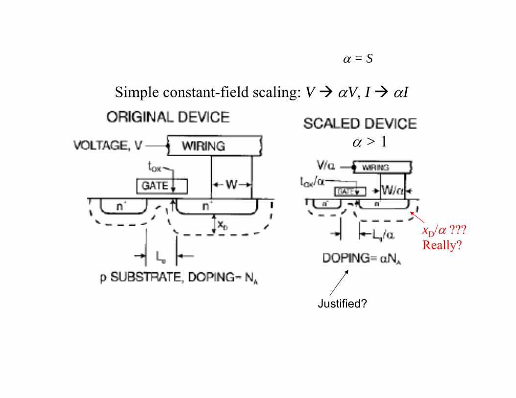
(S > 1)
Scale all dimensions and voltages by the same factor, so the field does not change, and the device physics will be about the same. Makes sense at the first glance.
Will talk about these later

Constant filed constant current density
W’ = W/S ID’ = ID/S
(holds for every instant)
Device resistance R = V/ILoad capacitance C = CoxWL. C’ = C/S
Switch delay time ~ RC. ’ = /S
fT (VG Vth)/L2 or fT vsat/L How’s fT doing?
Why? And why not so true?
(A/cm)
(S > 1)

(to make some economic sense by being compatible)
Switching delay time 1/S2
(S > 1)
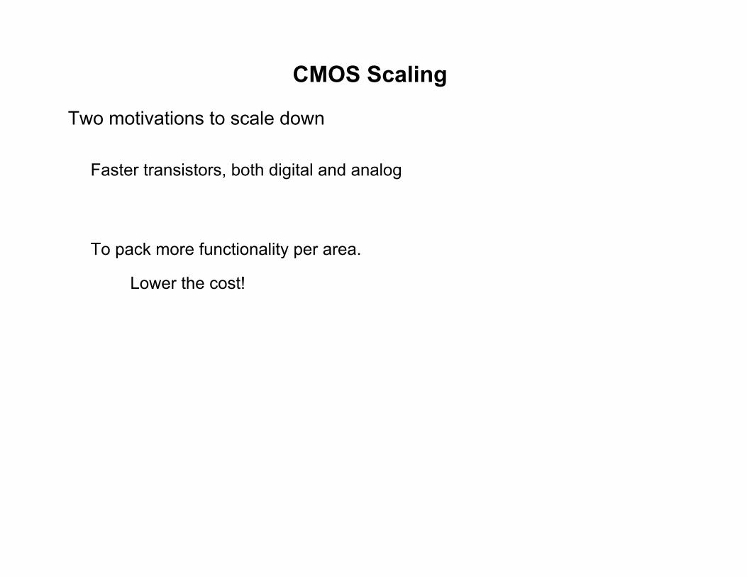
Moore’s Law
• Gordon E. Moore (born 1929), a co-founder of Intel
• Moore's Law is the empirical observation made in 1965 that the number of transistors on an integrated circuit for minimum component cost doubles every 24 months (sometimes quoted as 18 months).
• Moore's law is not about just the density of transistors that can be achieved, but about the density of transistors at which the cost per transistor is the lowest.
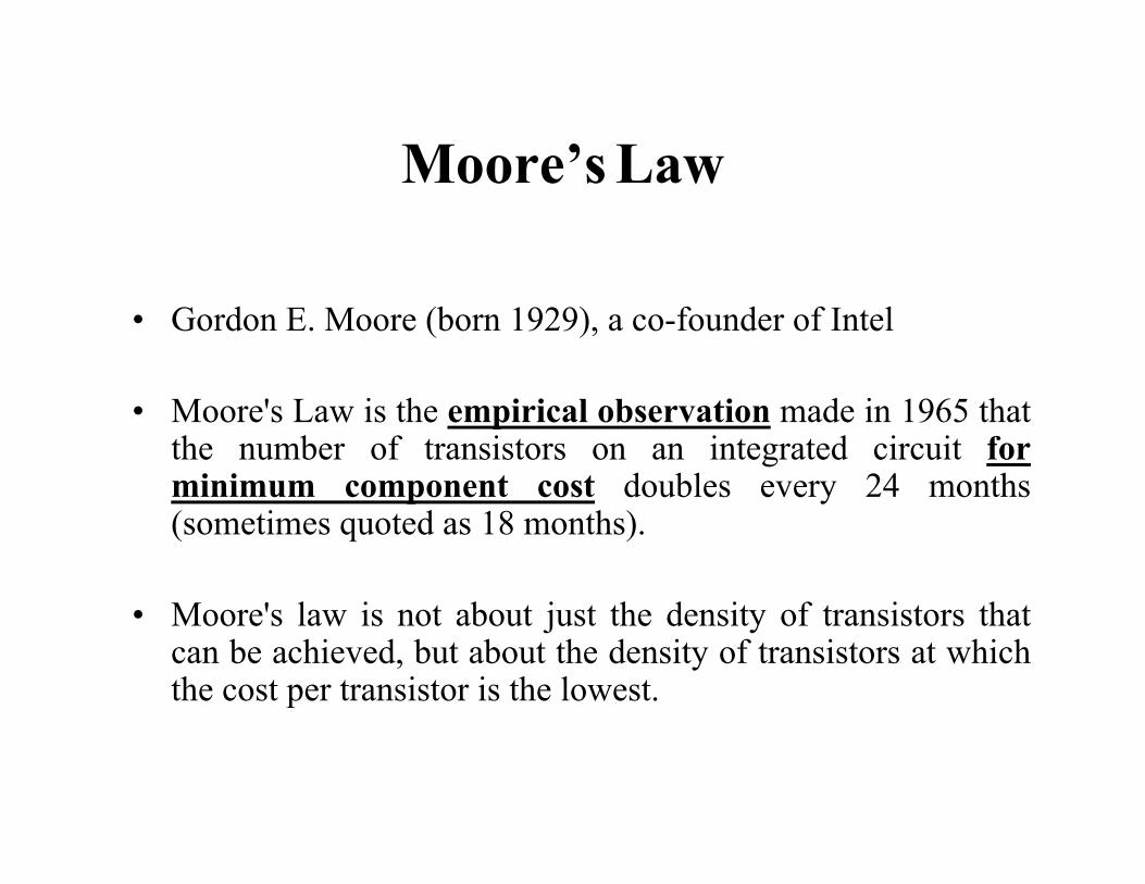
Why Small (if they are already so small that we can’t make them better)? • To pack more functionality into each unit area
- With feature size shrinking and wafer size growing, more and better products each wafer – better economics
Transistor radio!1965: $1/transistor
2006: 1 “microdolar”/transistor

2017, ~10 nm
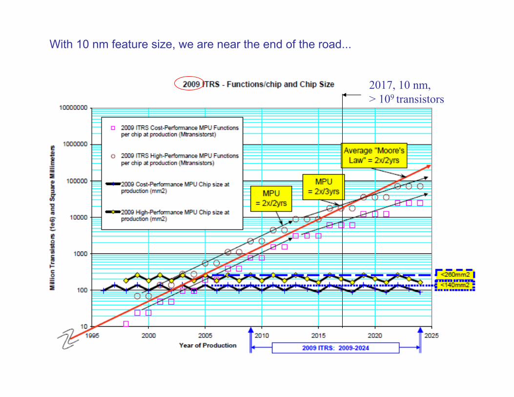
2017, 10 nm,> 109 transistors
With 10 nm feature size, we are near the end of the road...
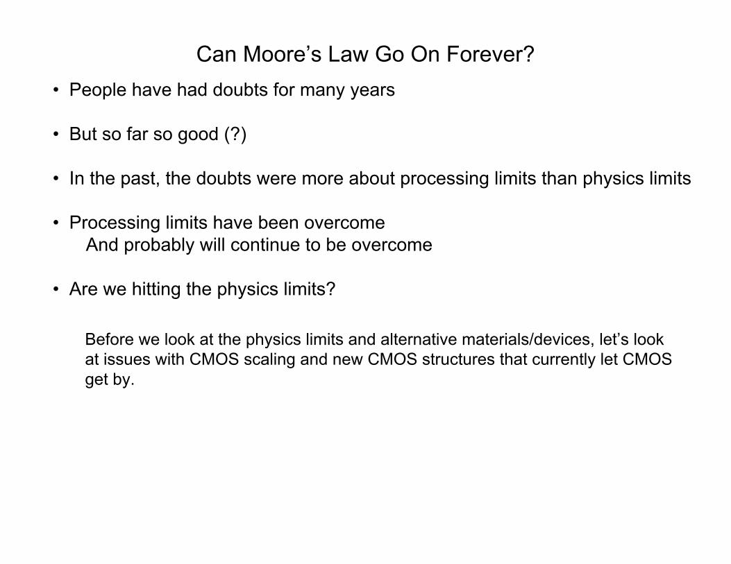
Can Moore’s Law Go On Forever?• People have had doubts for many years
• But so far so good (?)
• In the past, the doubts were more about processing limits than physics limits
• Processing limits have been overcomeAnd probably will continue to be overcome
• Are we hitting the physics limits?
Before we look at the physics limits and alternative materials/devices, let’s look at issues with CMOS scaling and new CMOS structures that currently let CMOS get by.
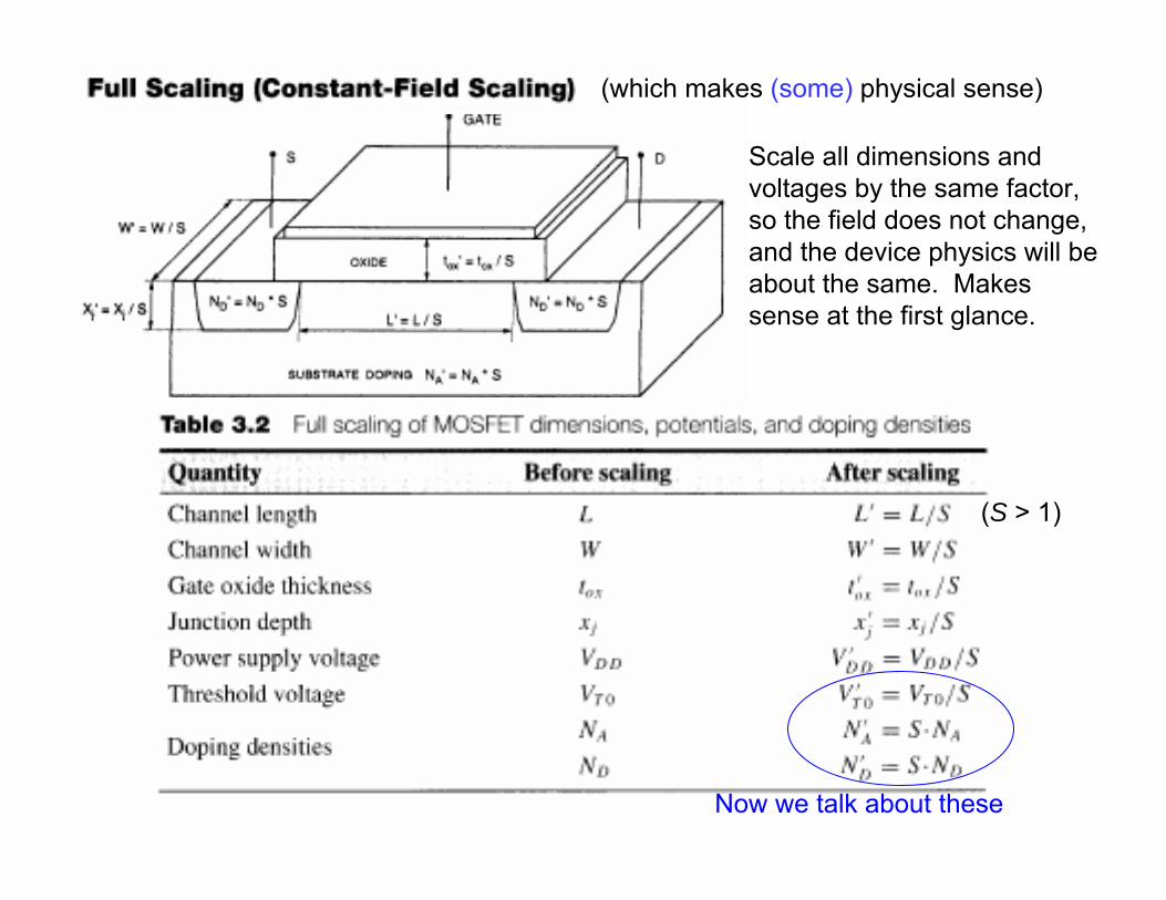
(which makes (some) physical sense)
(S > 1)
Scale all dimensions and voltages by the same factor, so the field does not change, and the device physics will be about the same. Makes sense at the first glance.
Now we talk about these

Constant filed constant current density
W’ = W/S ID’ = ID/S
But we did not say why. Let’s now have a closer look.
Areal carrier charge density in channel qn = Eox
e’s per area
n = n’
Js = qnElateral
A/cm A/cmcmV
cmC
Vscm
2
2
ID = JsW
Js’ = Js
ID’ = ID/S
(A/cm)
if we truly have constant field
> 1
xD/ ???Really?
Simple constant-field scaling: V V, I I
= S
Justified?
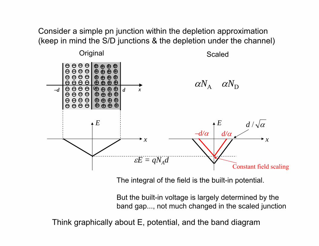
Consider a simple pn junction within the depletion approximation(keep in mind the S/D junctions & the depletion under the channel)
x0 dd x0 dd
x
E
Think graphically about E, potential, and the band diagram
x
E
NDNA
d/d/
Constant field scaling
But the built-in voltage is largely determined by the band gap..., not much changed in the scaled junction
/d
Original Scaled
E = qNAd
The integral of the field is the built-in potential.

(which makes (some) physical sense)
Not exactly
AiADd NnNNx /)/ln( 2
ox
pApFBth C
qNVV
)2(22
Doesn’t scale.Need Vth adjustment.
(S > 1)
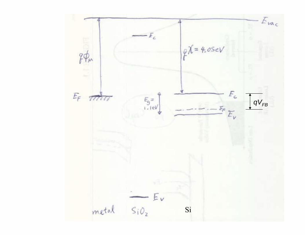
Si
qVFB

Work out the details of constant-voltage scaling offline
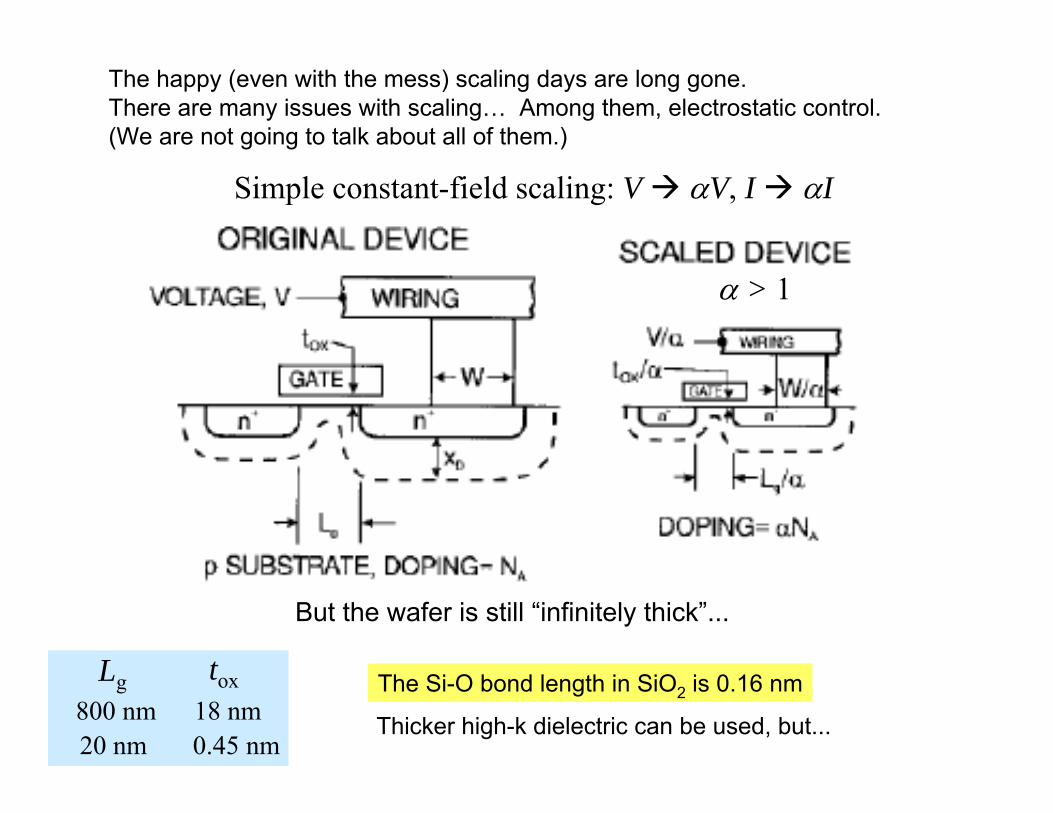
The happy (even with the mess) scaling days are long gone.There are many issues with scaling… Among them, electrostatic control.(We are not going to talk about all of them.)
> 1
Lg tox800 nm 18 nm20 nm 0.45 nm
The Si-O bond length in SiO2 is 0.16 nm
Thicker high-k dielectric can be used, but...
But the wafer is still “infinitely thick”...
Simple constant-field scaling: V V, I I

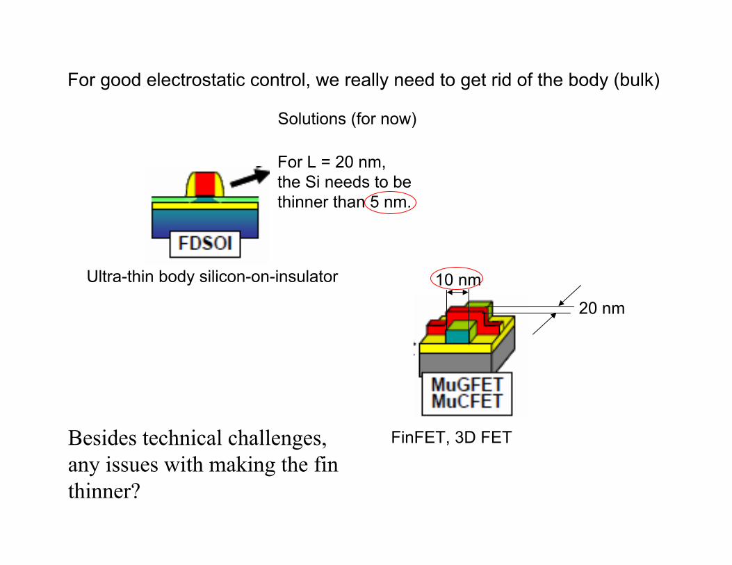
Solutions (for now)
Ultra-thin body silicon-on-insulator
FinFET, 3D FET
20 nm
10 nm
For L = 20 nm, the Si needs to be thinner than 5 nm.
For good electrostatic control, we really need to get rid of the body (bulk)
Further reading: “Transistor Wars,” IEEE spectrum, November 2011http://spectrum.ieee.org/semiconductors/devices/transistor-wars

Will need very high NA for the substrate, to scale down the xd of the S/D junctions, as well as the xdmax of the FET channel. This will cause high S-to-D leakage.
Carrier density
Thin bodies don’t have to be doped. No need for depletion Lower vertical fields
Deplete and then invert.
The bulk is a path for leakage.
Why is SOI a challenge?http://en.wikipedia.org/wiki/Silicon_on_Insulator
Solutions (for now)
Ultra-thin body silicon-on-insulator
FinFET, 3D FET
20 nm
10 nm
For L = 20 nm, the Si needs to be thinner than 5 nm.
For good electrostatic control, we really need to get rid of the body (bulk)
Besides technical challenges, any issues with making the fin thinner?

http://www.webelements.com/silicon/crystal_structure.html http://onlineheavytheory.net/silicon.html
Crystal structure of Si
If several monolayers thin, is Si still the Si as we know it?

33 = 27(32)3 = 1
103 = 1000(102)3 = 512
Half of the small cubes are on the surface!

Can Moore’s Law Go On Forever?• People have had doubts for many years
• But so far so good (?)
• In the past, the doubts were more about processing limits than physics limits
• Processing limits have been overcomeAnd probably will continue to be overcome
• Are we hitting the physics limits?
Forget about details.The crystal constant of Si is 0.54 nm.
Fundamental scaling limit: 10 nm wall?10 nm is only ~19 crystal constants!
Do the (semi-classical) semiconductor physics theories we rely on still work?
Are there alternatives to scaling to achieve faster devices?


One alternative is semiconductors in which electrons travel faster.(If our goal were only to make the device faster.)
fT = vsat /(2L)
Si
Ashley et al, IEEE IEDL ’97, 751 (1997).
But economics is in the driver’s seat…
Reading: Ye, III-V MOSFETs (posted on course website).

How thin can Si (or any 3D stuff) go?For a 3D material, if we make it a few atoms thin, it’s no longer that material as we know it!(Recall that 10X10X10 cube)
Graphene is 2D.It’s 1-atom thin by nature.The “ultimate SOI” if we put it on an insulator.
If it ever (?) becomes the post-Sisemiconductor, its 2D nature (actually, we may need to turn it into 1D) probably deserves more kudos than its fast moving electrons.
The need for lower dimensional materials

At the end of the road, we look for alternatives.We want things that are inherently low dimensional (2D or 1D)
Graphite: 3D but layered (w/ van der Waals gaps)
Graphene: 2D
Carbon nanotube: (quasi-)1DMoS2
No gap
Gap
Gap or no gap

https://spectrum.ieee.org/semiconductors/devices/how-well-put-a-carbon-nanotube-computer-in-your-hand
Carbon nanotube FETs are considered promising.
1D. Good electrostatic control.
Challenges:To achieve uniform diameter and chirality (for uniform band gap)To place them into a dense, parallel array
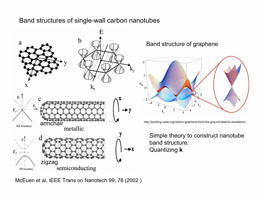
McEuen et al, IEEE Trans on Nanotech 99, 78 (2002 )
http://exciting-code.org/carbon-graphene-from-the-ground-state-to-excitations
Band structures of single-wall carbon nanotubes
Band structure of graphene
Simple theory to construct nanotubeband structure:Quantizing k
zigzag
armchair

https://www.frontiersin.org/articles/10.3389/fchem.2015.00059/full
Carbon nanotube indexing
Simple theory (not exact):n m = multiple of 3 metallicTherefore, armchair (n,n) always metallic, zigzag (n,0) metallic when n = multiple of 3, semiconducting otherwise.
Now you see how challenge it is to get all tubes to have the same bandwidth
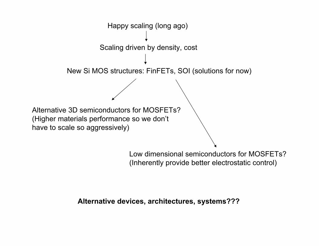
Happy scaling (long ago)
Scaling driven by density, cost
New Si MOS structures: FinFETs, SOI (solutions for now)
Alternative 3D semiconductors for MOSFETs?(Higher materials performance so we don’t have to scale so aggressively)
Low dimensional semiconductors for MOSFETs?(Inherently provide better electrostatic control)
Alternative devices, architectures, systems???

Old
?
?
?


![Ebooksclub[1].Org Electronic Device Architectures for the Nano CMOS Era From Ultimate CMOS Scaling to Beyond CMOS Devices](https://img.pdfslide.us/doc/110x75/55720d47497959fc0b8c5b0f/ebooksclub1org-electronic-device-architectures-for-the-nano-cmos-era-from-ultimate-cmos-scaling-to-beyond-cmos-devices.jpg)