Embed Size (px)
Citation preview

www.nanohub.orgNCN
ECE606: Solid State DevicesECE606: Solid State DevicesLecture 26: Schottky Diode (II)
Muhammad Ashraful [email protected]
Alam ECE‐606 S09 1

OutlineOutline
1) DC Thermionic current (detailed derivation)
2) AC small signal and large‐signal response
3) Additional information
4) Conclusions
Ref. SDF, Chapter 14
Alam ECE‐606 S09 2Alam ECE‐606 S092

Energy Resolved Thermionic Flux occupation
( )min
E Eυ
β∞ ∞ − Ω∫ ∫ ∫
~ DOS
( )34
Fs x xm
E Ey zJ q dk edk dk β υ
π− −
→−∞ −∞−∞
Ω= − ∫ ∫ ∫
minυ
V
q(Vbi‐VA)VA
EC‐EF
Alam ECE‐606 S09 3
x
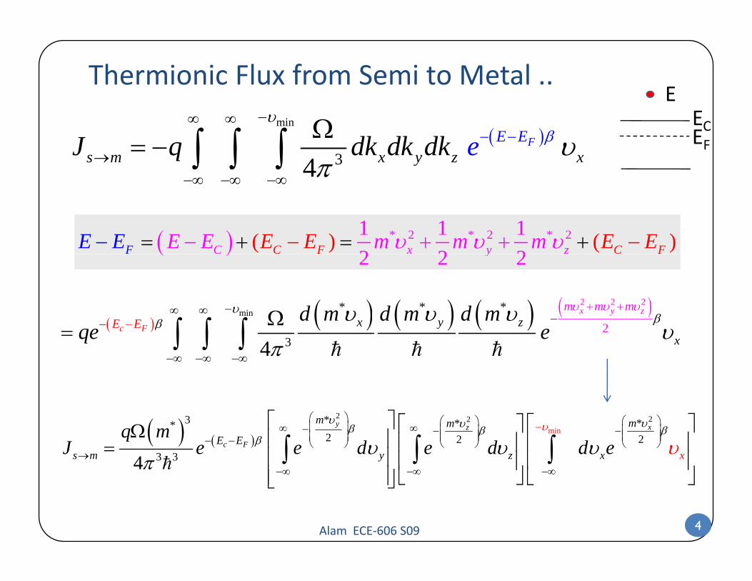
Thermionic Flux from Semi to Metal .. E
( )min
34F
s m x y z xE EJ q dk dk edk β
υ
υπ
−∞ ∞
→−
∞ −∞ −∞
−
−
Ω= − ∫ ∫ ∫
ECEF
∞ −∞ −∞−
( ) * 2 * 2 * 21 1 12 2
( ) ( )2C x y zC F C FF E E E EE E m m mE E υ υ υ− + ++− =− −= +
( ) ( ) ( ) ( ) ( )min2 2 2* *
2
* x y
c F
zx y z
m m mE E d m d m d m υυ υ
ββυυ υ υ−∞ ∞
−−+
−+
Ω∫ ∫ ∫
( )2 2 2y
( ) ( ) ( ) ( )2
34c F y
xE Eqe eβ υ
π−∞ −∞ −∞
= ∫ ∫ ∫
( ) ( )
2 22min
3 * ***2 22
3 34
y xz
c F
m mmE E
s m y z x x
q mJ e e d e d d e
υ υυβ βυββ υ υ υ υ
π
⎛ ⎞ ⎛ ⎞⎛ −⎞⎜ ⎟∞ ∞− −− ⎜ ⎟⎜ ⎟⎜ ⎟ ⎜ ⎟ ⎜ ⎟− − ⎝ ⎠ ⎝ ⎠ ⎝ ⎠→
−∞ −∞ −∞
⎡ ⎤ ⎡ ⎤⎡ ⎤Ω ⎢ ⎥ ⎢ ⎥⎢ ⎥= ⎢ ⎥ ⎢ ⎥⎢ ⎥⎣ ⎦ ⎣ ⎦⎢ ⎥⎣ ⎦
∫ ∫ ∫
Alam ECE‐606 S09 4
∞ ∞ ∞⎣ ⎦ ⎣ ⎦⎢ ⎥⎣ ⎦

Thermionic Current … ( )min *
2bi A
q V Vm
= −υ
( ) ( )
2 22min
3 * ***2 22
y xz
c F
m mmE Eq m
J e e d e d d eυ υυ υβ ββ
β υ υ υ υ
⎛ ⎞ ⎛ ⎞⎛ ⎞ −⎜ ⎟∞ ∞− −− ⎜ ⎟⎜ ⎟⎜ ⎟ ⎜ ⎟ ⎜ ⎟− ⎝ ⎠ ⎝ ⎠ ⎝ ⎠−⎡ ⎤ ⎡ ⎤⎡ ⎤Ω ⎢ ⎥ ⎢ ⎥⎢ ⎥= ⎢ ⎥ ⎢ ⎥⎢ ⎥∫ ∫ ∫
m
3 34s m y z x xJ e e d e d d eυ υ υ υπ→
−∞ ∞ −∞−⎢ ⎥ ⎢ ⎥⎢ ⎥
⎣ ⎦ ⎣ ⎦⎢ ⎥⎣ ⎦∫ ∫ ∫
( )1bi AV Vqe β−−
* 24 k
π π 2bi Ae
( )2
203
4 bF C i A AE E qV qV Vqs m
qm kJ T e e A eh
β β βπ→
− −= =
( )0 1AqT s m m s
VJ J J A e β→ →= − = −
5
Compare with p‐n junction … where is the bandgap, doping?
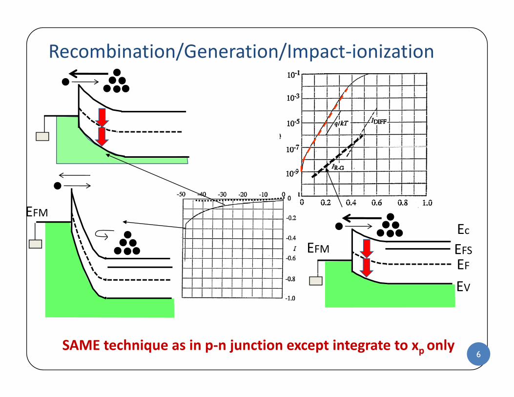
Recombination/Generation/Impact‐ionization
EFMEc
EFEFSEFM
EV
6SAME technique as in p‐n junction except integrate to xp only

Outline
1) DC Thermionic current (detailed derivation)
2) AC small signal and large‐signal response
3) Additional information
4) Conclusions
Alam ECE‐606 S09 7

Topic Map
Equilibrium DC Small Large CircuitsEquilibrium DC Small signal
Large Signal
Circuits
Diode
Schottky
BJT/HBT
MOS
Alam ECE‐606 S09 8

AC response
ConductanceJunction Capacitance
Series
Capacitance
ResistanceDiffusion Capacitance
Alam ECE‐606 S09 9
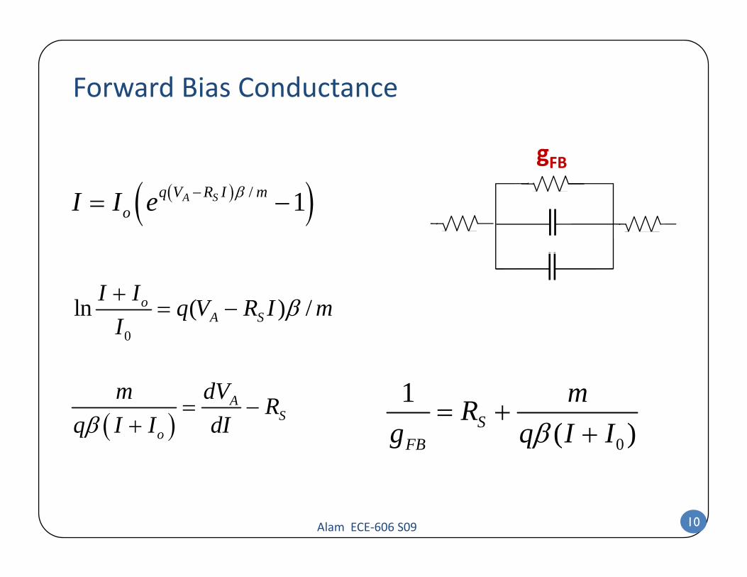
Forward Bias Conductance
gFB( )( )/ 1A Sq V R I m
oI I e −= −β
ln ( ) /oA S
I I q V R I mI+
= − β
1 m
0I
Am dV
0
1( )S
FB
mRg q I I
= ++β( )
AS
o
m dV Rq I I dI
= −+β
Alam ECE‐606 S09 10

Junction Capacitance (Majority Carriers)
Junction Capacitance
0s AC κ ε=JC
W=
Aκ ε 0
02 ( )
sJ
sbi A
ACV V
qN
κ εκ ε
=−
Alam ECE‐606 S09 11
DqN

No Diffusion Capacitance in Schottky Diode
p‐n Diode Schottky diode
n
x
VA
No minority carrier transport and
Alam ECE‐606 S09 12
No minority carrier transport and therefore no diffusion capacitance ..

Reducing diffusion capacitance in p‐n diode
p‐n Diode Schottky dioden
x
VA
13
Short minority carrier lifetime in p-n junction diode equivalent to rapid energy relaxation in SB diode.

Outline
1) DC Thermionic current (detailed derivation)
2) AC small signal and large‐signal response
3) Additional information
4) Conclusions
Alam ECE‐606 S09 14
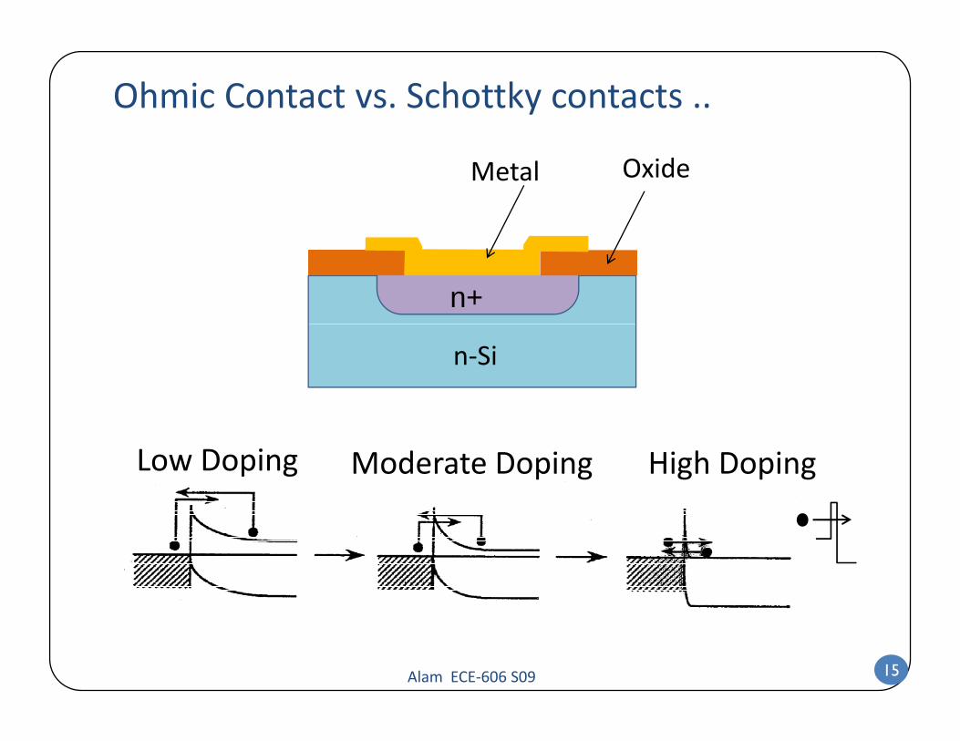
Ohmic Contact vs. Schottky contacts ..
OxideMetal
n+
n‐Si
Low Doping Moderate Doping High Doping
Alam ECE‐606 S09 15

Lowering of Schottky Barrier
E
qφ1qφB qφ1qφB
SemiMetal
‐I
Metal Semi
‐‐
‐‐‐
‐
‐Surface Charge
ElectronImage Charge
Alam ECE‐606 S09 16Ref. Sze/Ng., p. 143x
Chargex

Fermi‐level PinningDensity of States
Ec
Regardless the workfunction, no modulation in potential. (e g Modern high-k dielectrics)
Full
Full
EcEf
Ev
(e.g. Modern high k dielectrics)
Metal MetalSemiconductor
EcE
Shift in the Band edge
Full
Metal
Full
Metal
Ef
Ev
Alam ECE‐606 S09 17
A BMetalMetal

Conclusion
1) Schottky diodes have wide range of applications in
practical devices.
2) The key distinguishing feature of Schottky diode is that
it is a majority carrier device.it is a majority carrier device.
3) We use a different technique to calculate the current in
a majority carrier device It is called thermionica majority carrier device. It is called thermionic
emission.
Alam ECE‐606 S09 18