Embed Size (px)
Citation preview

Department of Electrical and Computer Engineering
© Vishal Saxena -1-
ECE518 Memory/Clock Synchronization IC Design
Dr. Vishal Saxena
Electrical and Computer Engineering DepartmentBoise State University, Boise, ID
Integer-N Frequency Synthesizers

© Vishal Saxena -2-
Outline
Basic Synthesizer PLL-Based Modulation Divider Design
Settling Behavior Spur Reduction
Techniques
Settling Behavior Spur Reduction
Techniques In-Loop Modulation Offset-PLL TX In-Loop Modulation Offset-PLL TX Pulse-Swallow Divider
Dual-Modulus Dividers CML and TSPC
Techniques Miller and Injection-
Locked Dividers
Pulse-Swallow Divider Dual-Modulus Dividers CML and TSPC
Techniques Miller and Injection-
Locked Dividers

© Vishal Saxena -3-
General Considerations: Why Do We Need Synthesizers?
The synthesizer performs the precise setting of LO frequency
A slight shift leads to significant spillage of a high-power interferer in to a desired channel
© Vishal Saxena -4-
Wireless Standards
Difficult LO design → narrower channel spacing and stringent phase noise/spur requirements
LO for GSM receiver is the hardest
© Vishal Saxena -5-
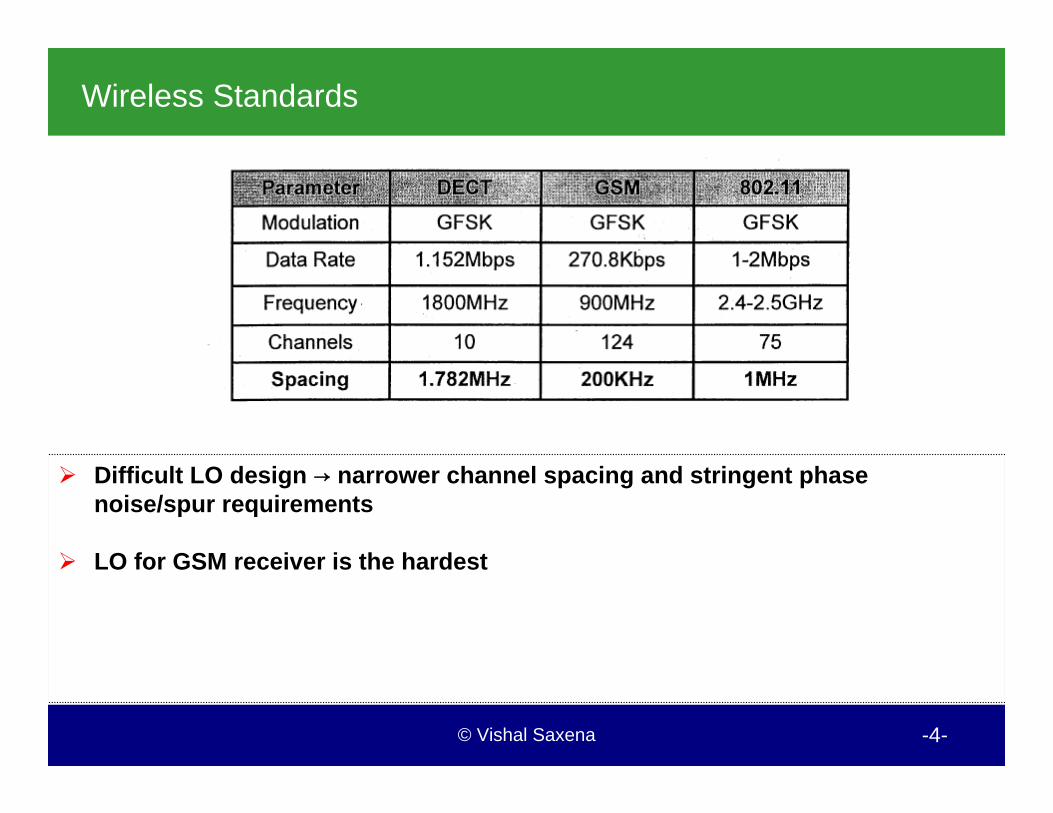
Reciprocal Mixing The output frequency is generated as a multiple of
a precise reference. Sidebands: upon downconversion mixing, the
desired channel is convolved with the carrier and the interferer with the sideband

© Vishal Saxena -6-
Example of Reciprocal Mixing and Intermodulation
A receiver with an IIP3 of -15 dBm senses a desired signal and two interferers as shown in figure below. The LO also exhibits a sideband at ωS, corrupting the downconversion. What relative LO sideband magnitude creates as much corruption as intermodulation does?
To compute the level of the resulting intermodulation product that falls into the desired channel, we write the difference between the interferer level and the IM3 level in dB as
(The IM3 level is equal to -90 dBm.) Thus, if the sideband is 50 dB below the carrier, then the two mechanisms lead to equal corruptions.

© Vishal Saxena -7-
Lock Time
Lock time directly subtracts from the time available for communication
The lock time is typically specified as the time required for the output frequency to reach within a certain margin around its final value

© Vishal Saxena -8-
Example of Lock Time
Solution:
If the power amplifier remains on, then the LO frequency variations produce large fluctuations in the transmitted carrier during the settling time. Shown in figure above, this effect can considerably corrupt other users’ channels.
During synthesizer settling, the power amplifier in a transmitter is turned off. Explain why.

© Vishal Saxena -9-
Basic Integer-N Synthesizer
Integer-N synthesizer produce an output frequency that is an integer multiple of the reference frequency.
The choice of fREF: it must be equal to the desired channel spacing and it must be the greatest common divisor of f1 and f2.

© Vishal Saxena -10-
Example of Reference Frequency and Divide Ratio Selection
Compute the required reference frequency and range of divide ratios for an integer-N synthesizer designed for a Bluetooth receiver. Consider two cases: (a) direct conversion, (b) sliding-IF downconversion with fLO = (2/3)fRF
(a)Shown in (a), the LO range extends from the center of the first channel, 2400.5 MHz, to that of the last, 2479.5 MHz. Thus, even though the channel spacing is 1 MHz, fREF must be chosen equal to 500 kHz. Consequently, N1 = 4801 and N2 = 4959.
(b) As illustrated in (b), in this case the channel spacing and the center frequencies are multiplied by 2/3. Thus, fREF = 1/3 MHz, N1 = 4801, and N2 = 4959.

© Vishal Saxena -11-
Choosing N1 and N2
fin = GCD (fref, fout)
fref = 19.68MHz and fout = 2.402GHz →fin = 40 kHz
fref = 19.68MHz and fin = 40kHz →N1 = 492
fin = 40kHz and fout = 2.042GHz →N2 = 60050
Need programmable: 2.042GHz ≤ fout ≤ 2.480GHz
fout = 2.480GHz + m MHz with 2 ≤m≤78
→N2 = 60050 + 25∙m

© Vishal Saxena -12-
Settling Behavior: Channel Switching
When the divide ratio changes, the loop responds as if an input frequency step were applied
we can view multiplication by (1 –ε/A) as a step function from f0 to f0(1 – ε/A), i.e., a frequency jump of -(ε/A)f0.

© Vishal Saxena -13-
Worst Case Settling and Example of Error
The worse case occurs when the synthesizer output frequency must go from the first channel, N1fREF, to the last, N2fREF, or vice versa
In synthesizer settling, the quantity of interest is the frequency error, Δωout, with respect to the final value. Determine the transfer function from the input frequency to this error.
The error is equal to ωin[N -H(s)], where H(s) is the transfer function of a type-II PLL (Chapter 9). Thus,

© Vishal Saxena -14-
Calculation of Settling TimeAssuming N2 - N1 << N1
If the divide ratio jumps from N1 to N2, this change is equivalent to an input frequency step of Δωin = (N2 - N1)ωREF =N1.
For the normalized error to fall below a certain amount, α, we have
Where
For example, if ζ=

© Vishal Saxena -15-
Example of Settling Time CalculationA 900-MHz GSM synthesizer operates with fREF = 200 kHz and provides 128 channels. If ζ= , determine the settling time required for a frequency error of 10 ppm.
The divide ratio is approximately equal to 4500 and varies by 128, i.e., N1 ≈ 4500 and N2 - N1= 128. Thus,
or
While this relation has been derived for ζ = , it provides a reasonable approximation for other values of ζ up to about unity. How is the value of ζωn chosen? From Chapter 9, we note that the loop time constant is roughly equal to one-tenth of the input period. It follows that (ζωn)-1 ≈ 10TREF and hence
In practice, the settling time is longer and a rule of thumb for the settling of PLLs is 100 times the reference period.
© Vishal Saxena -16-
Spur Reduction Techniques: Will Scaling Down Transistor Widths Work?
Solution:
A student reasons that if the transistor widths and drain currents in a charge pump are scaled down, so is the ripple. Is that true?
This is true because the ripple is proportional to the absolute value of the unwanted charge pump injections rather than their relative value. This reasoning, however, can lead to the wrong conclusion that scaling the CP down reduces the output sideband level. Since a reduction in IP must be compensated by a proportional increase in KVCO so as to maintain _ constant, the sideband level is almost unchanged.

© Vishal Saxena -17-
Spur Reduction Techniques: Masking the Ripple by Insertion of a Switch
Vcont is disturbed for a short duration (at the phase comparison instant) and remains relatively constant for the rest of the input period.
The arrangement of (a) leads to an unstable PLL Topology of (b) can yield a stable PLL
(a) (b)

© Vishal Saxena -18-
Stabilization of PLL by Adding K1 to the Transfer Function of VCO (Ⅰ)
Open-loop transfer function of a type-II second-order PLL
Can we realize: to obtain a zero?
Indeed, K1 represents a variable-delay stage having a “gain” of K1:

© Vishal Saxena -19-
Stabilization of PLL by Adding K1 to the Transfer Function of VCO (Ⅱ)
With Divider

© Vishal Saxena -20-
Stabilization of PLL by Adding K1 to the Transfer Function of VCO: Modified Architecture
A retiming flipflop can be inserted between the delay line and the PFD to remove the phase noise of the former
© Vishal Saxena -21-
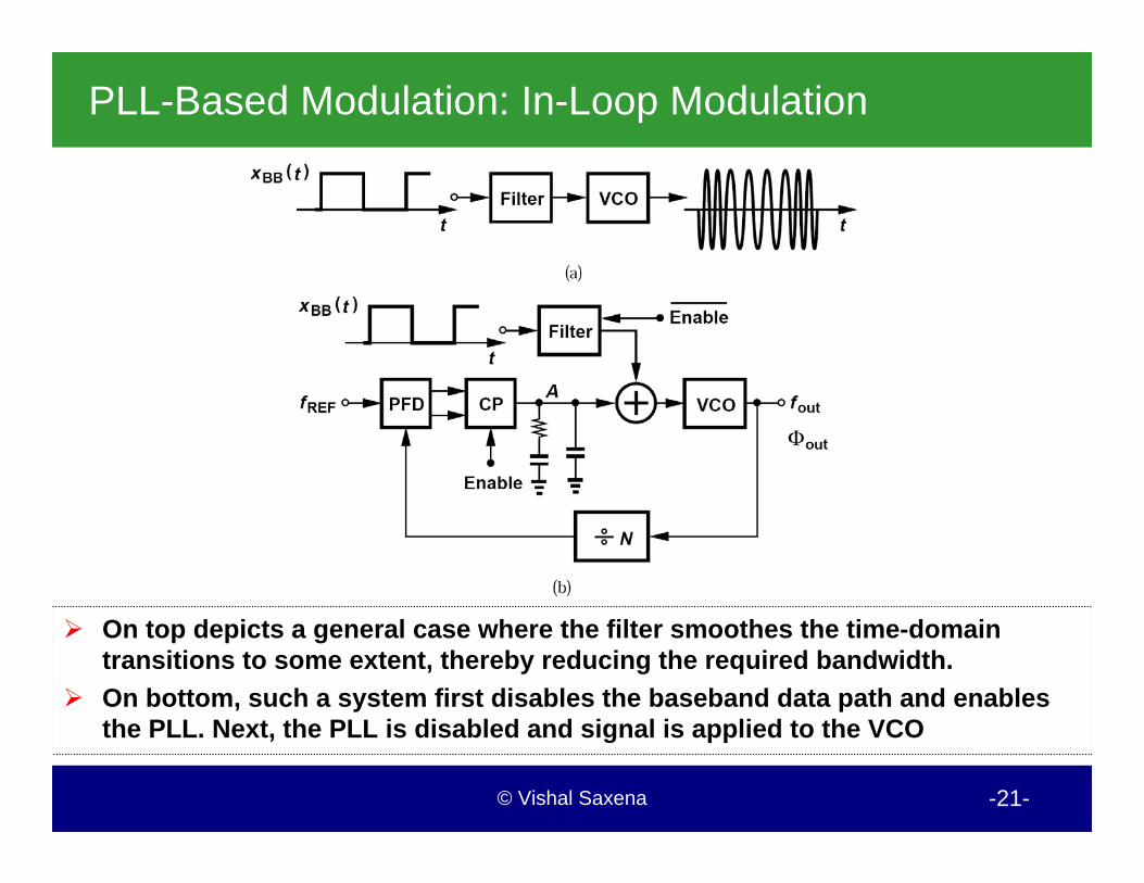
PLL-Based Modulation: In-Loop Modulation
On top depicts a general case where the filter smoothes the time-domain transitions to some extent, thereby reducing the required bandwidth.
On bottom, such a system first disables the baseband data path and enables the PLL. Next, the PLL is disabled and signal is applied to the VCO

© Vishal Saxena -22-
Drawbacks of Previous Arrangement and Modification
Architecture above requires periodic “idle” times during the communication to phase-lock the VCO
The output signal bandwidth depends on KVCO, a poorly-controlled parameter.
The free-running VCO frequency may shift from NfREF due to a change in its load capacitance or supply voltage
To alleviate the foregoing issues, the VCO can remain locked while sensing the baseband data
The design must select a very slow loop so that the desired phase modulation at the output is not corrected by the PLL
© Vishal Saxena -23-
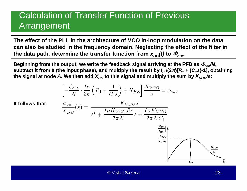
Calculation of Transfer Function of Previous Arrangement
Beginning from the output, we write the feedback signal arriving at the PFD as Φout/N, subtract it from 0 (the input phase), and multiply the result by IP /(2π)[R1 + (C1s)-1], obtaining the signal at node A. We then add XBB to this signal and multiply the sum by KVCO/s:
The effect of the PLL in the architecture of VCO in-loop modulation on the data can also be studied in the frequency domain. Neglecting the effect of the filter in the data path, determine the transfer function from xBB(t) to Φout.
It follows that

© Vishal Saxena -24-
Modulation by Offset PLLs
The noise transmitted by user C corrupts the desired signal around f1
In direct-conversion transmitters, each stage in the signal path contributes noise, producing high output noise in the RX band even if the baseband LPF suppresses the out-of-channel DAC output noise

© Vishal Saxena -25-
Example of Noise Floor at Previous Arrangement
Solution:
If the signal level is around 632 mVpp (= 0 dBm in a 50-Ω system) at node X figure above, determine the maximum tolerable noise floor at this point. Assume the following stages are noiseless.
The noise floor must be 30 dB lower than that at the PA output, i.e., -159 dBm/Hz in a 50-Ωsystem. Such a low level dictates very small load resistors for the upconversion mixers. In other words, it is simply impractical to maintain a sufficiently low noise floor at each point along the TX chain.
© Vishal Saxena -26-
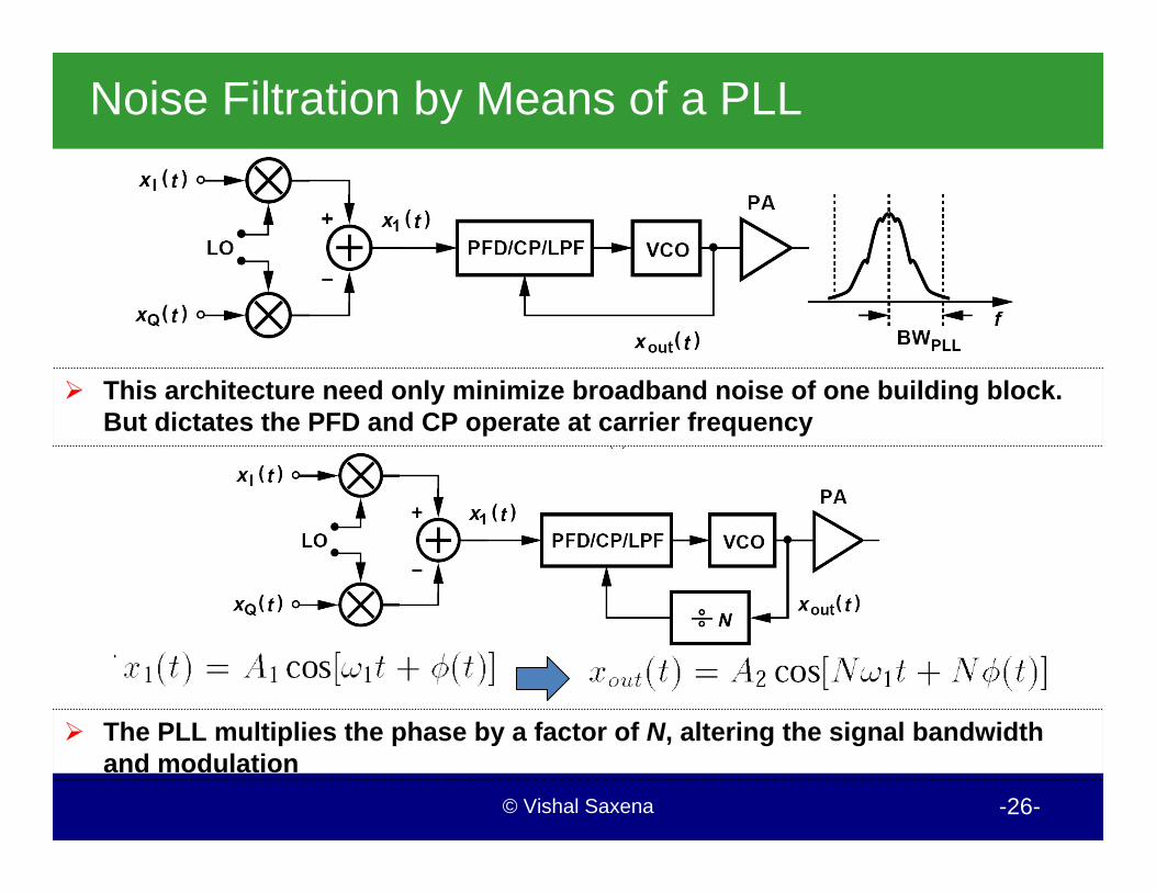
Noise Filtration by Means of a PLL
This architecture need only minimize broadband noise of one building block. But dictates the PFD and CP operate at carrier frequency
The PLL multiplies the phase by a factor of N, altering the signal bandwidth and modulation

© Vishal Saxena -27-
Offset-PLL Architecture
With the loop locked, x1(t) must become a faithful replica of the reference input, thus containing no modulation. Consequently, yI(t) and yQ(t) “absorb” the modulation information of the baseband signal.

© Vishal Saxena -28-
Example of Offset-PLL Architecture
Solution:
If xI (t) = Acos[Φ(t)] and xQ(t) = Asin[Φ(t)], derive expressions for yI (t) and yQ(t).
Centered around fREF, yI and yQ can be respectively expressed as
where ωREF = 2πfREF and Φy(t) denotes the phase modulation information. Carrying the quadrature upconversion operation and equating the result to an unmodulated tone, x1(t) = Acos ωREF t, we have
It follows that
And hence
Note that xout(t) also contains the same phase information

© Vishal Saxena -29-
Another Example of Offset-PLL Architecture
Solution:
In the architecture above, the PA output spectrum is centered around the VCO center frequency. Is the VCO injection-pulled by the PA?
To the first order, it is not. This is because, unlike TX architectures studied in Chapter 4, this arrangement impresses the same modulated waveform on the VCO and the PA. In other words, the instantaneous output voltage of the PA is simply an amplified replica of that of the VCO. Thus, the leakage from the PA arrives in-phase with the VCO waveform—as if a fraction of the VCO output were fed back to the VCO. In practice, the delay through the PA introduces some phase shift, but the overall effect on the VCO is typically negligible.

© Vishal Saxena -30-
Divider Design: Requirements
The divider modulus, N, must change in unity steps
The first stage of the divider must operates as fast as the VCO
The divider input capacitance and required input swing must be commensurate with the VCO drive capability
The divider must consume low power, preferably less than the VCO
© Vishal Saxena -31-
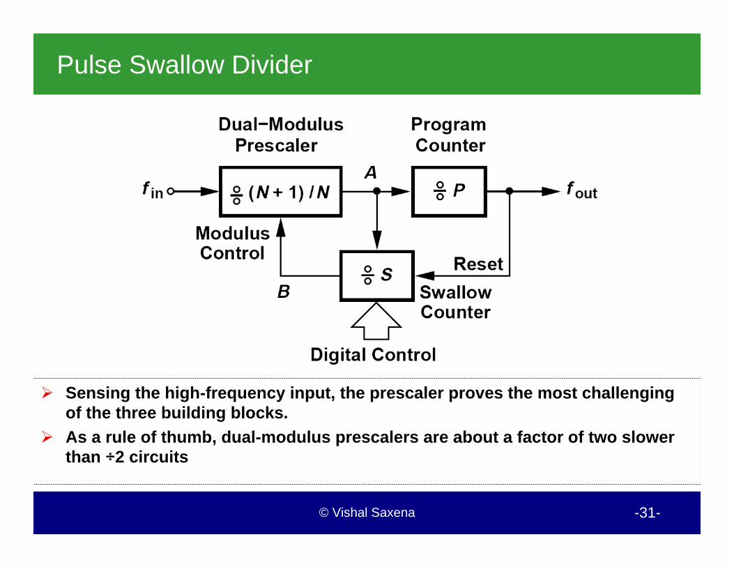
Pulse Swallow Divider
Sensing the high-frequency input, the prescaler proves the most challenging of the three building blocks.
As a rule of thumb, dual-modulus prescalers are about a factor of two slower than ÷2 circuits

© Vishal Saxena -32-
Pulse Swallow Divider
S pulses counted with a (N+1) modulus, and remaining (P-S) pulses counted with a N modulus
Adding the total number of pulses at the prescalar input in the two modes (N+1)S + N(P-S) = NP + S
Thus, for every NP+S pulse at the main input, the PC generates one pulse at the output.

© Vishal Saxena -33-
Example of Preceding the Pulse Swallow Divider by a ÷2
Solution:
In order to relax the speed required of the dual-modulus prescaler, the pulse swallow divider can be preceded by a ÷2. Explain the pros and cons of this approach.
Here, fout = 2(NP + S)fREF . Thus, a channel spacing of fch dictates fREF = fch=2. The lock speedand the loop bandwidth are therefore scaled down by a factor of two, making the VCO phase noise more pronounced. One advantage of this approach is that the reference sideband lies at the edge of the adjacent channel rather than in the middle of it. Mixed with little spurious energy, the sidebands can be quite larger than those in the standard architecture.
© Vishal Saxena -34-
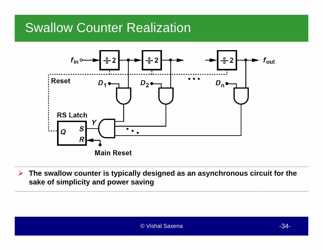
Swallow Counter Realization
The swallow counter is typically designed as an asynchronous circuit for the sake of simplicity and power saving

© Vishal Saxena -35-
Modular Divider Realizing Multiple Divider Ratios
This method incorporates ÷2/3 stages in a modular form so as to reduce the design complexity. Each ÷2/3 block receives a modulus control from the next stage. The digital inputs set the overall divide ratio according to:
Suppose the circuit begins with Q1Q2 = 00. next three cycles, Q1Q2 goes to 10, 11, and 01. Note that the state Q1Q2 = 00 does not occur again because it would require the previous values of Q2 and X to be ZERO and ONE, respectively,
Divide- by-3 Circuit:
© Vishal Saxena -36-
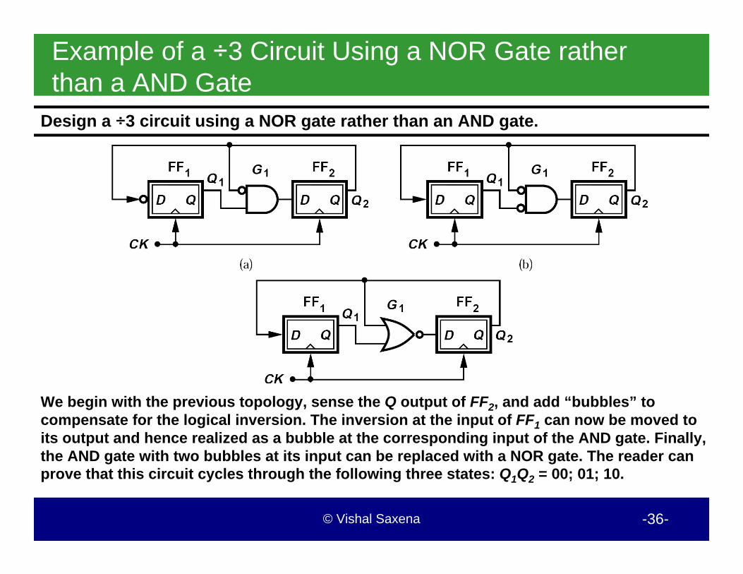
Example of a ÷3 Circuit Using a NOR Gate rather than a AND Gate
Design a ÷3 circuit using a NOR gate rather than an AND gate.
We begin with the previous topology, sense the Q output of FF2, and add “bubbles” to compensate for the logical inversion. The inversion at the input of FF1 can now be moved to its output and hence realized as a bubble at the corresponding input of the AND gate. Finally, the AND gate with two bubbles at its input can be replaced with a NOR gate. The reader can prove that this circuit cycles through the following three states: Q1Q2 = 00; 01; 10.

© Vishal Saxena -37-
Speed Limitation of the ÷3 Stage
Analyze the speed limitations of the ÷3 stage shown in Fig. 10.28
We draw the circuit as above, explicitly showing the two latches within FF2. Suppose CK is initially low, L1 is opaque (in the latch mode), and L2 is transparent (in the sense mode). In other words, Q2 has just changed. When CK goes high and L1 begins to sense, the value of Q2 must propagate through G1 and L1 before CK can fall again. Thus, the delay of G1 enters the critical path. Moreover, L2 must drive the input capacitance of FF1, G1, and an output buffer. These effects degrade the speed considerably, requiring that CK remain high long enough for Q2 to propagate to Y .

© Vishal Saxena -38-
Divide-by-2/3 Circuit
The ÷2/3 circuit employs an OR gate to permit ÷3 operation if the modulus control, MC, is low or ÷2 operation if it is high
A student seeking a low-power prescaler design surmises that FF1 in the ÷ 3 circuit can be turned off when MC goes high. Explain whether this is a good idea.
While saving power, turning off FF1 may prohibit instantaneous modulus change because when FF1 turns on, its initial state is undefined, possibly requiring an additional clock cycle to reach the desired value. For example, the overall circuit may begin with Q1Q2 = 00.
© Vishal Saxena -39-
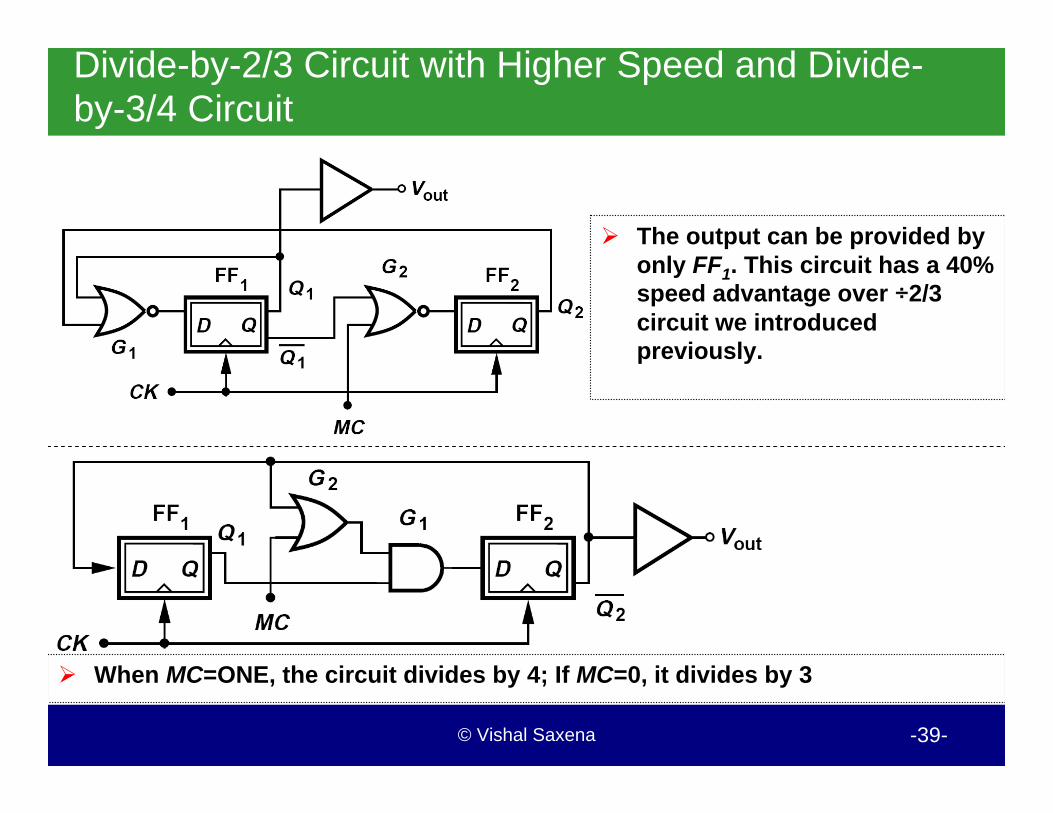
Divide-by-2/3 Circuit with Higher Speed and Divide-by-3/4 Circuit
The output can be provided by only FF1. This circuit has a 40% speed advantage over ÷2/3 circuit we introduced previously.
When MC=ONE, the circuit divides by 4; If MC=0, it divides by 3

© Vishal Saxena -40-
Divide-by-8/9 Circuit
For higher moduli, a synchronous core having small moduli is combined with asynchronous divider stages.
If MC2 is low, MC1 is high, the overall circuit operates as a ÷8 circuit; if MC2 is high, the circuit divides by 9.
© Vishal Saxena -41-
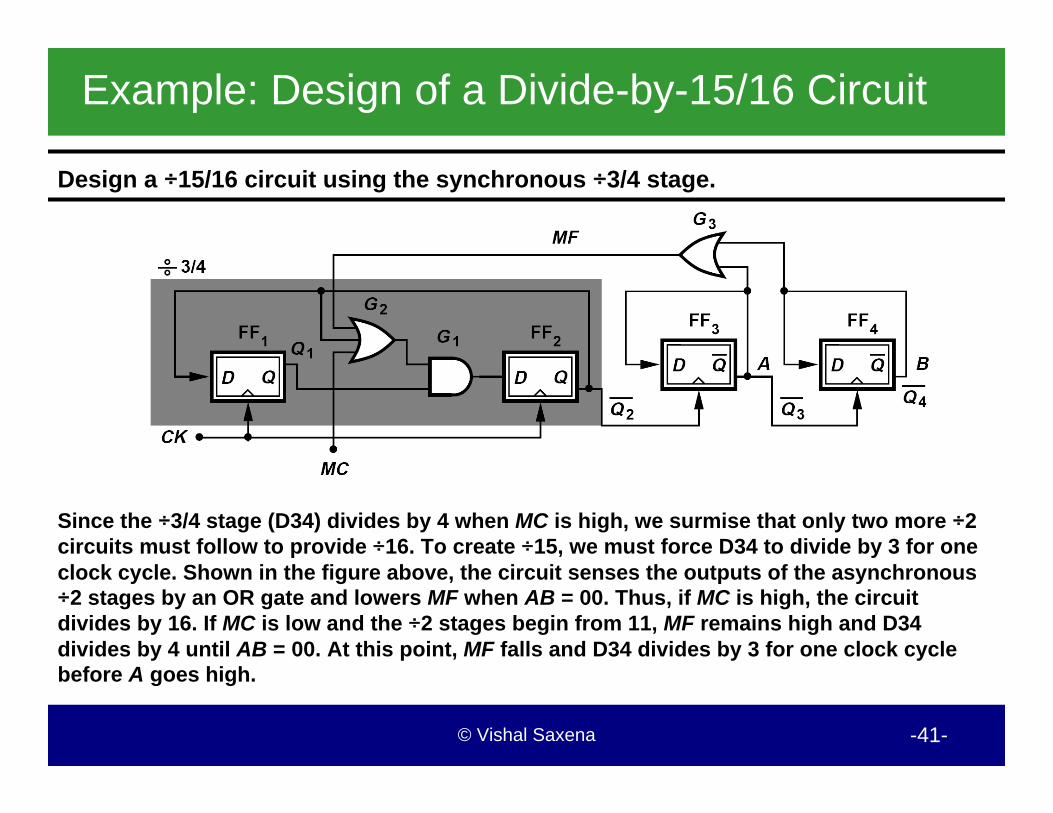
Example: Design of a Divide-by-15/16 Circuit
Design a ÷15/16 circuit using the synchronous ÷3/4 stage.
Since the ÷3/4 stage (D34) divides by 4 when MC is high, we surmise that only two more ÷2 circuits must follow to provide ÷16. To create ÷15, we must force D34 to divide by 3 for one clock cycle. Shown in the figure above, the circuit senses the outputs of the asynchronous ÷2 stages by an OR gate and lowers MF when AB = 00. Thus, if MC is high, the circuit divides by 16. If MC is low and the ÷2 stages begin from 11, MF remains high and D34 divides by 4 until AB = 00. At this point, MF falls and D34 divides by 3 for one clock cycle before A goes high.

© Vishal Saxena -42-
Potential Race Conditions
First suppose FF3 and FF4 change their output state on the rising edge of their clock inputs. If MC is low, the circuit continues to divide by 16. As in (a), state 00 is skipped. The propagation delay through FF3 and G3 need not be less than a cycle of CKin
In the case FF3 and FF4 change their output state on the falling edge of their clock inputs, the ÷3/4 circuit must skip the state 00. This is in general difficultto achieve, complicating the design and demanding higher power dissipation. Thus the first choice is preferable.
© Vishal Saxena -43-
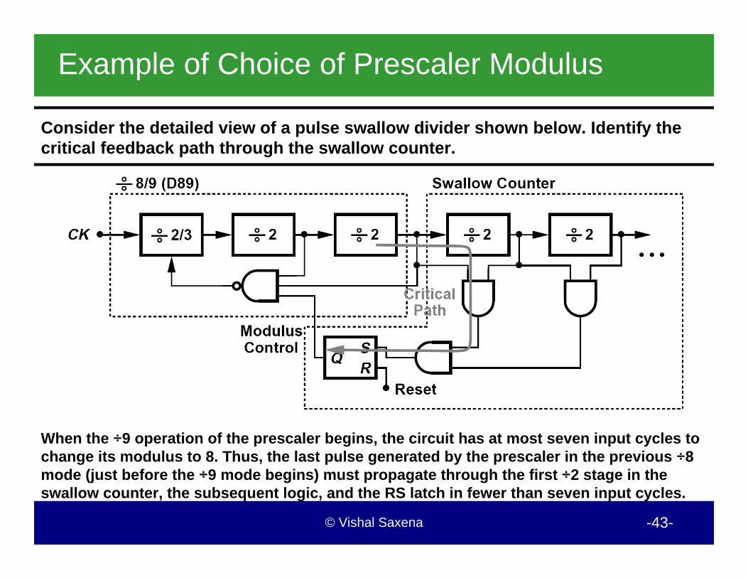
Example of Choice of Prescaler Modulus
Consider the detailed view of a pulse swallow divider shown below. Identify the critical feedback path through the swallow counter.
When the ÷9 operation of the prescaler begins, the circuit has at most seven input cycles to change its modulus to 8. Thus, the last pulse generated by the prescaler in the previous ÷8 mode (just before the ÷9 mode begins) must propagate through the first ÷2 stage in the swallow counter, the subsequent logic, and the RS latch in fewer than seven input cycles.

© Vishal Saxena -44-
Divider Logic Styles: True Single-Phase Clocking
When CK is high, the first stage operates as an inverter, impressing D at A and E. When CK goes low, the first stage is disabled and the second stage becomes transparent, writing A at B and C and hence making Q equal to A. The logical high at E and the logical low at B are degraded but the levels at Aand C ensure proper operation of the circuit.

© Vishal Saxena -45-
TSPC Divide-by-2 Circuit / Incorporating a NAND Gate
This topology achieves relatively high speeds with low power dissipation, but, unlike CML dividers, it requires rail-to-rail clock swings for proper operation.
The circuit consumes no static power and as a dynamic logic topology, the divider fails at very low clock frequencies due to the leakage of the transistors.
A NAND gate can be merged with the master latch.
In the design of TSPC circuit, one observes that wider clocked devices raises the maximum speed, but at the cost of loading the preceding stage.

© Vishal Saxena -46-
TSPC Using Ratioed Logic
The slave latch is designed as “ratioed” logic, achieving higher speeds.
Solution:
The first stage in figure above is not completely disabled when CK is low. Explain what happens if D changes in this mode.
If D goes from low to high, A does not change. If D falls, A rises, but since M4 turns off, it cannot change the state at B. Thus, D does not alter the state stored by the slave latch.

© Vishal Saxena -47-
Divider Logic Styles-Current Steering Circuit
CML operates with moderate input and output swings, and providesdifferential outputs and hence a natural inversion.
The circuit above is typically designed for a single-ended output swing of RDISS= 300mV, and the transistors are sized such that they experience complete switching with such input swings

© Vishal Saxena -48-
Problem of Common-Mode Compatibility at NAND Inputs
NAND gate is preceded by two representative CML stages. RT shifts the CM level of B and B by RTISS2. The addition of RT appears simple,
but now the high level of F and F is constrained if M5 and M6 must not enter the triode region

© Vishal Saxena -49-
Choice at Low Supply Voltages
The CML NOR/OR gate, avoid stacking. This stage operates only with single-ended inputs.
Should M1-M3 in figure above have equal widths?
One may postulate that, if both M1 and M2 are on, they operate as a single transistor and absorb all of ISS1, i.e., W1 and W2 need not exceed W3/2. However, the worst case occurs if only M1 or M2 is on. Thus, for either transistor to “overcome” M3, we require that W1 = W2 ≥W3.

© Vishal Saxena -50-
CML XOR Implementation
The topology is identical to the Gilbert cell mixer. As with the CML NAND gate, this circuit requires proper CM level shift and does not easily operate with low supply voltages.
While lending itself to low supply voltage, this topology senses each of the inputs in single-ended form, facing issues similar to those of the NOR gate.

© Vishal Saxena -51-
Speed Attributes of CML Latch
Speed advantage of CML circuits is especially pronounced in latches. The latch operates properly even with a limited bandwidth at X and Y if (a) in
the sense mode VX and VY begin from their full levels and cross, and (b) in the latch mode, the initial difference between VX and VY can be amplified to a final value of ISSRD

© Vishal Saxena -52-
Example to Formulate Regenerative Amplification (Ⅰ)
Solution:
Formulate the regenerative amplification of the above circuit in regeneration mode if VX - VY begins with an initial value of VXY0.
If VXY0 is small, M3 and M4 are near equilibrium and the small-signal equivalent circuit can be constructed as shown above. Here, CD represents the total capacitance seen at X and Y to ground, including CGD1 + CDB1 + CGS3 + CDB3 + 4CGD3 and the input capacitance of the next stage. The gate-drain capacitance is multiplied by a factor of 4 because it arises from both M3 and M4 and it is driven by differential voltages. Writing a KCL at node X gives
© Vishal Saxena -53-
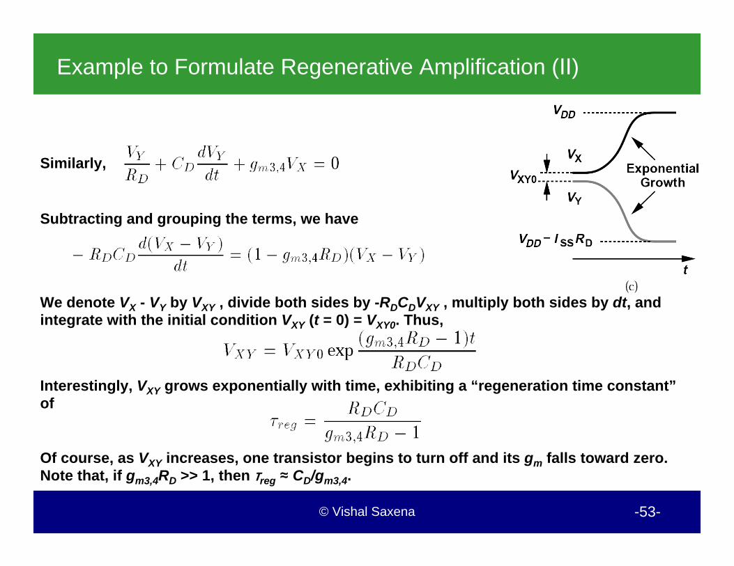
Example to Formulate Regenerative Amplification (Ⅱ)
Similarly,
Subtracting and grouping the terms, we have
We denote VX - VY by VXY , divide both sides by -RDCDVXY , multiply both sides by dt, and integrate with the initial condition VXY (t = 0) = VXY0. Thus,
Interestingly, VXY grows exponentially with time, exhibiting a “regeneration time constant”of
Of course, as VXY increases, one transistor begins to turn off and its gm falls toward zero. Note that, if gm3,4RD >> 1, then τreg ≈ CD/gm3,4.

© Vishal Saxena -54-
Example to Derive Relation Between Circuit Parameters and Clock Period
Suppose the D latch of the CML latch must run with a minimum clock period ofTck, spending half of the period in each mode. Derive a relation between the circuit parameters and Tck. Assume the swings in the latch mode must reach at least 90% of their final value.Initial voltage difference
The minimum initial voltage must be established by the input differential pair in the sense mode [just before t = t3]. In the worst case, when the sense mode begins, VX and VY are at the opposite extremes and must cross and reach VXY0 in 0.5Tck seconds. For example, VYbegins at VDD and falls according to
Since VX - VY must reach VXY0 in 0.5Tck seconds, we have
© Vishal Saxena -55-
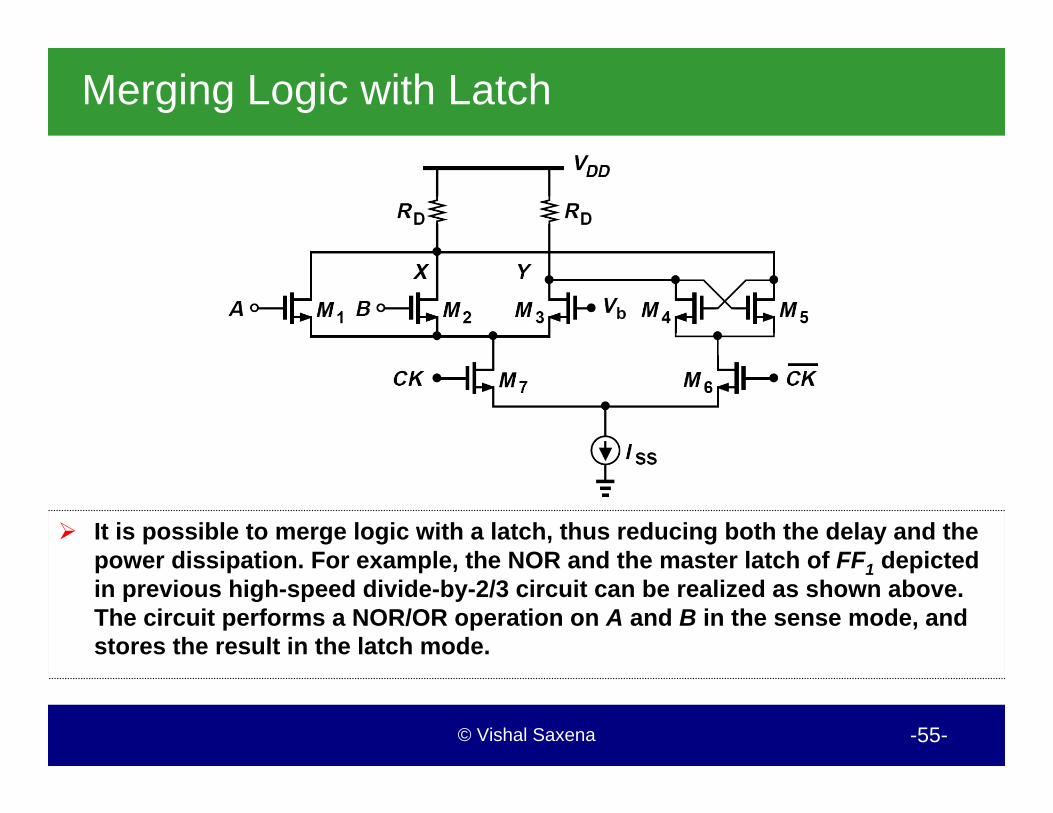
Merging Logic with Latch
It is possible to merge logic with a latch, thus reducing both the delay and the power dissipation. For example, the NOR and the master latch of FF1 depicted in previous high-speed divide-by-2/3 circuit can be realized as shown above. The circuit performs a NOR/OR operation on A and B in the sense mode, and stores the result in the latch mode.

© Vishal Saxena -56-
Design Procedure
(1)Select ISS based on the power budget (2)Select RDISS ≈ 300mV(3)Select (W/L)1,2 such that the diff. pair experiences nearly complete switching for a diff. input of 300mV (4)Select (W/L)3,4 so that small-signal gain around regenerative loop exceeds unity (5)Select (W/L)5,6 such that the clocked pair steers most of the tail current with the specified clock swing
© Vishal Saxena -57-
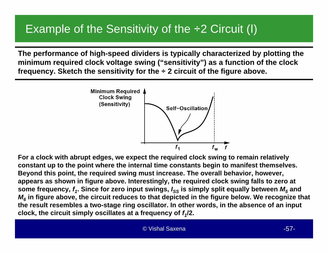
Example of the Sensitivity of the ÷2 Circuit (Ⅰ)
The performance of high-speed dividers is typically characterized by plotting the minimum required clock voltage swing (“sensitivity”) as a function of the clock frequency. Sketch the sensitivity for the ÷ 2 circuit of the figure above.
For a clock with abrupt edges, we expect the required clock swing to remain relatively constant up to the point where the internal time constants begin to manifest themselves. Beyond this point, the required swing must increase. The overall behavior, however, appears as shown in figure above. Interestingly, the required clock swing falls to zero at some frequency, f1. Since for zero input swings, ISS is simply split equally between M5 and M6 in figure above, the circuit reduces to that depicted in the figure below. We recognize that the result resembles a two-stage ring oscillator. In other words, in the absence of an input clock, the circuit simply oscillates at a frequency of f1/2.

© Vishal Saxena -58-
Example of the Sensitivity of the ÷2 Circuit (Ⅱ)
This observation provides another perspective on the operation of the divider: the circuit behaves as an oscillator that is injection-locked to the input clock. This viewpoint also explains why the clock swing cannot be arbitrarily small at low frequencies. Even with square clock waveforms, a small swing fails to steer all of the tail current, thereby keeping M2-M3 and M3-M4 simultaneously on. The circuit may therefore oscillate at f1/2 (or injection-pulled by the clock).
The “self-oscillation” of the divider also proves helpful in the design process: if the choice of device dimensions does not allow self-oscillation, then the divider fails to operate properly. We thus first test the circuit with a zero clock swing to ensure that it oscillates.

© Vishal Saxena -59-
Class-AB Latch
The bias of the clocked pair is defined by a current mirror and the clock is coupled capacitively.
Large clock swings allow transistors M5 and M6 to operate in the class AB mode, i.e., their peak current well exceed their bias current. This attribute improves the speed of the divider.
© Vishal Saxena -60-
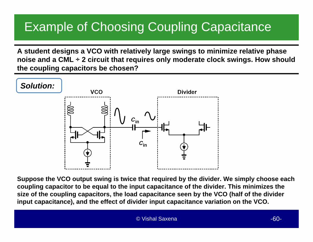
Example of Choosing Coupling Capacitance
Solution:
A student designs a VCO with relatively large swings to minimize relative phase noise and a CML ÷ 2 circuit that requires only moderate clock swings. How should the coupling capacitors be chosen?
Suppose the VCO output swing is twice that required by the divider. We simply choose each coupling capacitor to be equal to the input capacitance of the divider. This minimizes the size of the coupling capacitors, the load capacitance seen by the VCO (half of the divider input capacitance), and the effect of divider input capacitance variation on the VCO.

© Vishal Saxena -61-
CML Using Inductive Peaking
Rewrite this as
where
To determine the -3 dB bandwidth:
It follows that
© Vishal Saxena -62-
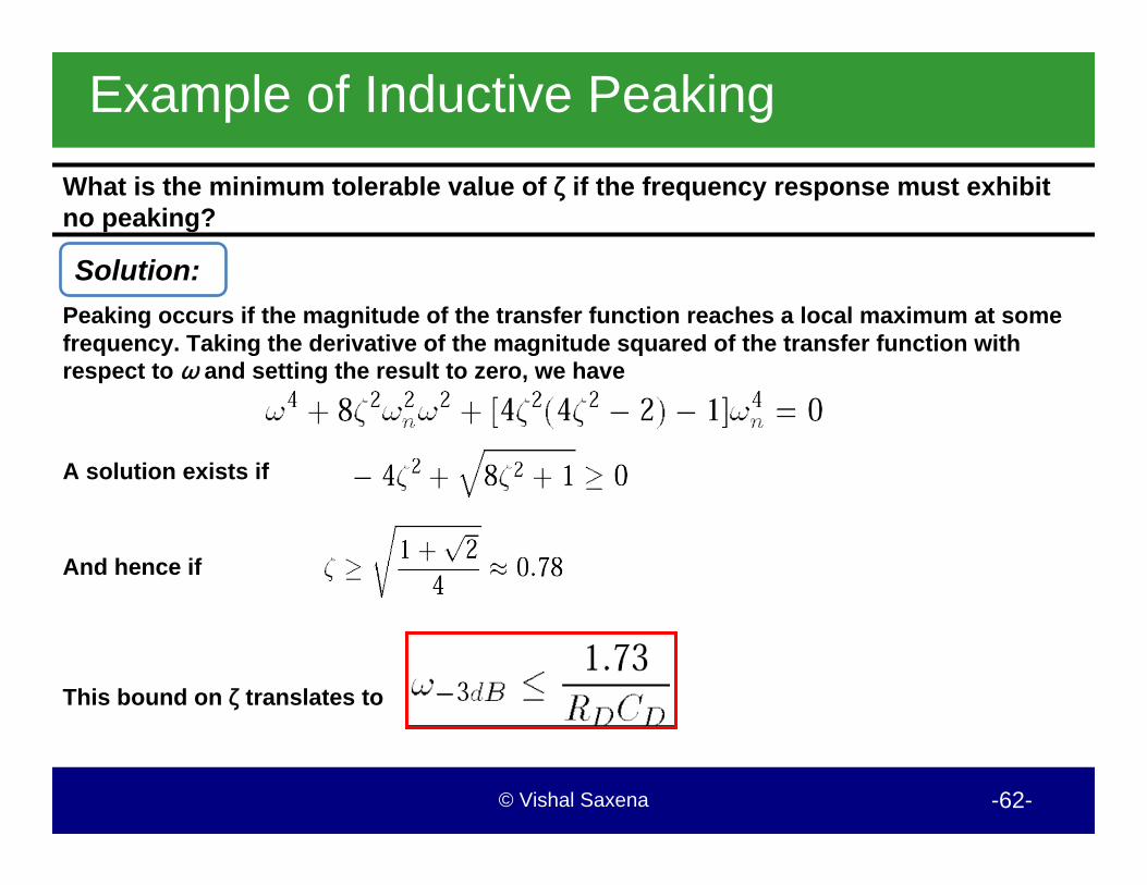
Example of Inductive Peaking
Solution:
What is the minimum tolerable value of ζ if the frequency response must exhibit no peaking?
Peaking occurs if the magnitude of the transfer function reaches a local maximum at some frequency. Taking the derivative of the magnitude squared of the transfer function with respect to ω and setting the result to zero, we have
A solution exists if
And hence if
This bound on ζ translates to
© Vishal Saxena -63-
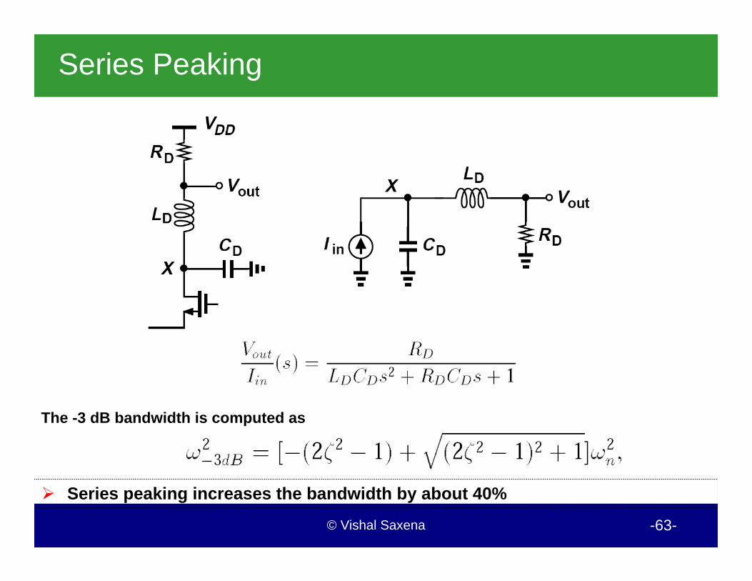
Series Peaking
Series peaking increases the bandwidth by about 40%
The -3 dB bandwidth is computed as

© Vishal Saxena -64-
Example of Series Peaking
Having understood shunt peaking intuitively, a student reasons that series peaking degrades the bandwidth because, at high frequencies, inductor LD in figure above impedes the flow of current, forcing a larger fraction of Iin to flow through CD. Since a smaller current flows though LD and RD, Vout falls at higher frequencies. Explain the flaw in this argument.
Let us study the behavior of the circuit at ωn = . As shown above, the Theveninequivalent of Iin, CD, and LD is constructed by noting that (a) the open-circuit output voltage is equal to Iin/(CDs), and (b) the output impedance (with Iin set to zero) is zero because CDand LD resonate at ωn. It follows that Vout = Iin=(CDs) at ω = ωn, i.e., as if the circuit consisted of only Iin and CD. Since Iin appears to flow entirely through CD, it yields a larger magnitude for Vout than if it must split between CD and RD.

© Vishal Saxena -65-
Series Peaking Circuit Driving Load Capacitance
Compared to shunt peaking, series peaking typically requires a smaller inductor value
What Happens if Load Inductor Increase?
As the value of LD becomes large enough, the circuit begins to fail at low frequencies. This is because the circuit approaches a quadrature LC oscillator that is injection-locked to the input clock

© Vishal Saxena -66-
Miller Divider
If the required speed exceeds that provided by CML circuits, one can consider the “Miller divider”, also known as the “dynamic divider”
The Miller divider can achieve high speeds for two reasons: (1) the low-pass behavior can simply be due to the intrinsic time constant at the output node of the mixer and (2) the circuit does not rely on latching and hence fails more gradually than flipflops as the input frequency increases

© Vishal Saxena -67-
Example of Miller Divider with Feedback
Solution:
Is it possible to construct a Miller divider by returning the output to the LO port of the mixer?
Shown above, such a topology senses the input at the RF port of the mixer. (Strangely enough, M3 and M4 now appear as diode-connected devices.) We will see below that this circuit fails to divide.

© Vishal Saxena -68-
Why the Component at 3fin/2 Must be Sufficiently Small?
This sum exhibits additional zero crossings, prohibiting frequency division if traveling through the LPF unchanged.

© Vishal Saxena -69-
Example of Miller Divider Using First-order Low-pass Filter
Does the arrangement shown below operate as a divider?
Since the voltage drop across R1 is equal to R1C1dVout/dt, we have VX = R1C1dVout/dt + Vout. Also, VX = αVinVout. If Vin = V0 cos ωint, then
It follows that
We integrate the left-hand side from Vout0 (initial condition at the output) to Vout and the right-hand side from 0 to t:
Thus
Interestingly, the exponential term drives the output to zero regardless of the values of α or ωin . The circuit fails because a one-pole filter does not sufficiently attenuate the third harmonic with respect to the first harmonic. An important corollary of this analysis is that the topology of Miller divider with feedback to switching quad cannot divide: the single-pole loop does not adequately suppress the third harmonic at the output.

© Vishal Saxena -70-
Introducing Phase Shift in Miller Divider
The Miller divider operates properly if the third harmonic is attenuated and shifted so as to avoid the additional zero crossings.

© Vishal Saxena -71-
Miller Divider with Inductive Load
If the load resistors are replaced with inductors, the gain-headroom and gain-speed trade-offs are greatly relaxed, but the lower end of the frequency range rises. Also the inductor complicates the layout.
The input frequency range across which the circuit operates properly is given by

© Vishal Saxena -72-
Example of Miller Divider with Inductive LoadsDoes the previous Miller divider with feedback to switching quad operate as a divider if the load resistors are replaced with inductors?
Depicted above left, such an arrangement in fact resembles an oscillator. Redrawing the circuit as shown right, we note M5 and M6 act as a cross-coupled pair and M3 and M4 as diode-connected devices. In other words, the oscillator consisting of M5-M6 and L1-L2 is heavily loaded by M3-M4, failing to oscillate (unless the Q of the tank is infinite or M3 and M4are weaker than M5 and M6). This configuration does operate as a divider but across a narrower frequency range.

© Vishal Saxena -73-
Miller Divider with Passive Mixers
Since the output CM level is near VDD, the feedback path incorporates capacitive coupling, allowing the sources and drains of M1-M4 to remain about 0.4V above the ground. The cross-coupled pair M7-M8 can be added to increase the gain by virtue of its negative resistance.
© Vishal Saxena -74-
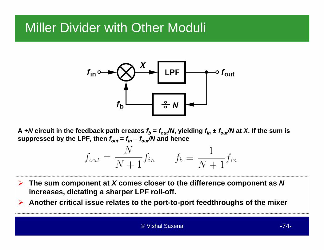
Miller Divider with Other Moduli
The sum component at X comes closer to the difference component as Nincreases, dictating a sharper LPF roll-off.
Another critical issue relates to the port-to-port feedthroughs of the mixer
A ÷N circuit in the feedback path creates fb = fout/N, yielding fin ± fout/N at X. If the sum is suppressed by the LPF, then fout = fin – fout/N and hence

© Vishal Saxena -75-
Example of Effect of Feedthrough
Assume N = 2 in figure above and study the effect of feedthrough from each input port of the mixer to its output.
Figure above shows the circuit. The feedthrough from the main input to node X produces a spur at fin. Similarly, the feedthrough from Y to X creates a component at fin/3. The output therefore contains two spurs around the desired frequency. Interestingly, the signal at Yexhibits no spurs: as the spectrum of figure above travels through the divider, the main frequency component is divided while the spurs maintain their spacing with respect to the carrier (Chapter 9). Shown above on right the spectrum at Y contains only harmonics and a dc offset. The reader can prove that these results are valid for any value of N.

© Vishal Saxena -76-
Miller Divider Using SSB Mixer
The Miller divider frequency range can be extended through the use of a single-sideband mixer. But this approach requires a broadband 90°phase shift, a very difficult design.
The use of SSB mixing prove useful if the loop contains a divider that generates quadrature outputs. Topology in (b) achieves a wide frequency range and generates quadrature outputs. But it requires quadrature LO phases.

© Vishal Saxena -77-
Injection-Locked Dividers Based on oscillators that are injection-
locked to a harmonic of their oscillation frequency
If fin varies across a certain “lock range”, the oscillator remains injection-locked to the fout-fincomponent at node X
Determine the divide ratio of the topology shown below if the oscillator remains locked.The mixer yields two components at node X, namely, fin – fout/N and fin + fout/N. If the oscillator locks to the former, then fin – fout/N = fout and hence
Similarly, if the oscillator locks to the latter then
The oscillator lock range must therefore be narrow enough to lock to only one of the two components.

© Vishal Saxena -78-
Implementation of ILD
The output frequency range across which the circuit remains locked is given by
The input lock range is twice this value:

© Vishal Saxena -79-
Divider Delay and Phase Noise: Effect of Divider Delay
The zero has two undesirable effects: it flattens the gain, pushing the gain crossover frequency to higher values (in principle, infinity), and it bends the phase profile downward.
This zero must remain well above the original unity-gain bandwidth of the loop:
A stage with a constant delay of ΔT

© Vishal Saxena -80-
Effect of Divider Phase Noise
The output phase noise of the divider directly adds to the input phase noise, experiencing the same low-pass response as it propagates to ϕout. In other words, ϕn,div is also multiplied by a factor of N within the loop bandwidth.
For the divider to contribute negligible phase noise, we must have

© Vishal Saxena -81-
Use of Retiming FF to Remove Divider Phase Noise
If the divider phase noise is significant, a retiming flipflop can be used to suppress its effect.
In essence, the retiming operation bypasses the phase noise accumulated in the divider chain.

© Vishal Saxena -82-
Examples of Retiming to Remove Divider Phase Noise
Solution:
Solution:
Compare the output phase noise of the above circuit with that of a similar loop that employs noiseless dividers and no retiming flipflop. Consider only the input phase noise.
The phase noise is similar. Invoking the time-domain view, we note that a (slow) displacement of the input edges by ΔT seconds still requires that the edges at Y be displaced by ΔT, which is possible only if the VCO edges are shifted by the same amount.
Does the retiming operation in figure above remove the effect of the divider delay?
No, it does not. An edge entering the divider still takes a certain amount of time before it appears at X and hence at Y . In fact, figure above indicates that VY is delayed with respect to VX by at most one VCO cycle. That is, the overall feedback delay is slightly longer in this case.

© Vishal Saxena -83-
Integer-N Synthesis Drawbacks
Improved resolution always comes at the expense of reduced update rate (ii.e. lower fref)
Lower update rate →lower bandwidth
Larger contribution of the VCO phase noise → larger power
Large settling time → increase channel switching times
Need: Large bandwidth and fine frequency resolution
Fractional-N Synthesis

© Vishal Saxena -84-
References (Ⅰ)

© Vishal Saxena -85-
References (Ⅱ)
© Vishal Saxena -86-
References (Ⅲ)

© Vishal Saxena -87-
References1. B. Razavi, “RF Microelectronics,” 2nd Ed., Prentice Hall, 2012.2. S. Palermo, ECEN620: Network Theory and Broadband Circuit Design 2012,
TAMU.3. P. Hanumolu, ECE 599, OSU.
![Clock Synchronization in WSN: from Traditional Estimation ...ycwu/Clock Synchronization in WSN_overvi… · Pairwise Synchronization: Gaussian case [1] • Synchronize node j to node](https://img.pdfslide.us/doc/110x75/5f8929217e699f4e040a8be7/clock-synchronization-in-wsn-from-traditional-estimation-ycwuclock-synchronization.jpg)