Embed Size (px)
Citation preview
1
ECE2262 Electric Circuits
Chapter 4: Operational Amplifier (OP-AMP) Circuits
2
4.1 Operational Amplifiers
3
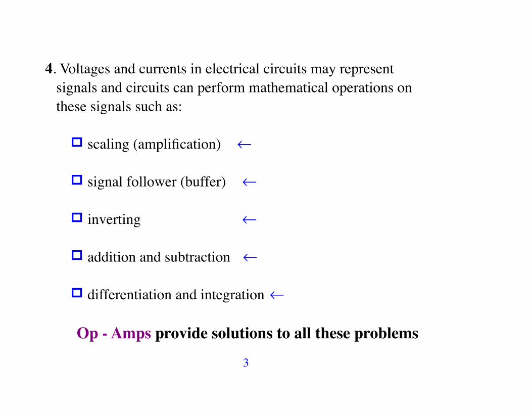
4. Voltages and currents in electrical circuits may represent signals and circuits can perform mathematical operations on these signals such as:
scaling (amplification) !
signal follower (buffer) !
inverting ! addition and subtraction !
differentiation and integration ! Op - Amps provide solutions to all these problems
4
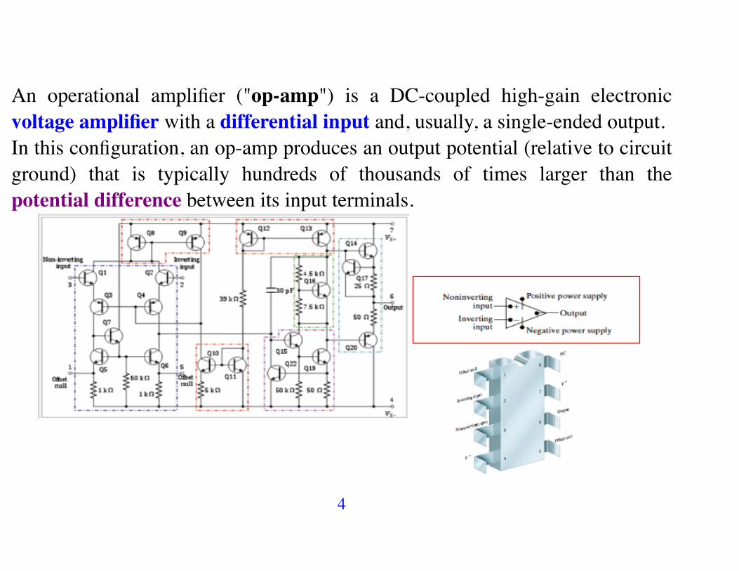
An operational amplifier ("op-amp") is a DC-coupled high-gain electronic voltage amplifier with a differential input and, usually, a single-ended output. In this configuration, an op-amp produces an output potential (relative to circuit ground) that is typically hundreds of thousands of times larger than the potential difference between its input terminals.
5
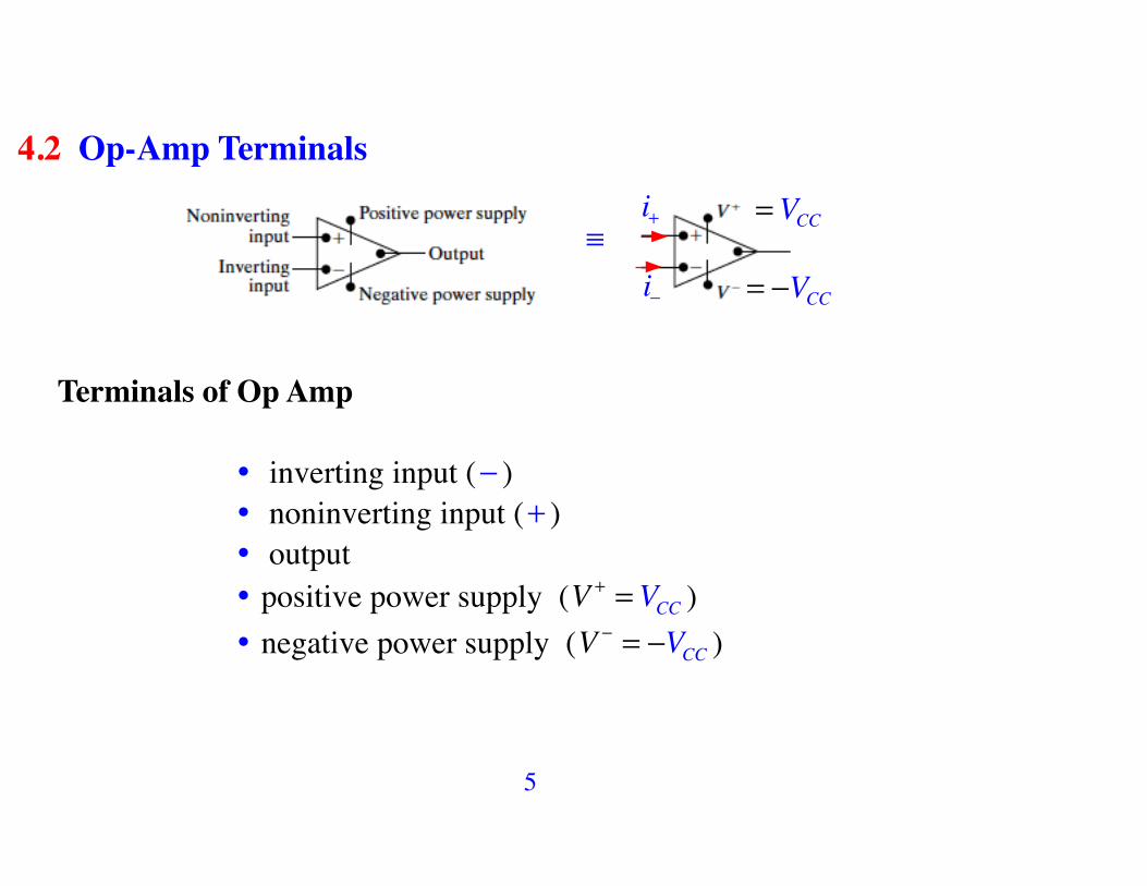
4.2 Op-Amp Terminals
!i+
i"
=VCC
= "VCC
Terminals of Op Amp
• inverting input (! )• noninverting input (+ )• output • positive power supply (V + =VCC )• negative power supply (V ! = !VCC )
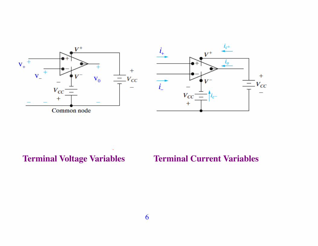
6
v+v!
i+
i!v0
Terminal Voltage Variables Terminal Current Variables
7
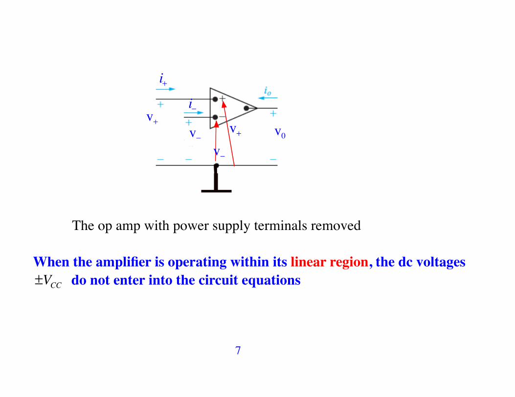
i+i!
v!v+
v0v+v!
The op amp with power supply terminals removed When the amplifier is operating within its linear region, the dc voltages ±VCC do not enter into the circuit equations
8
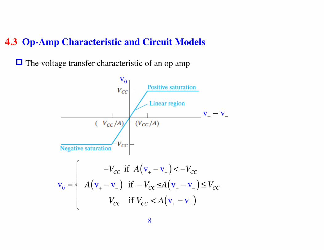
4.3 Op-Amp Characteristic and Circuit Models
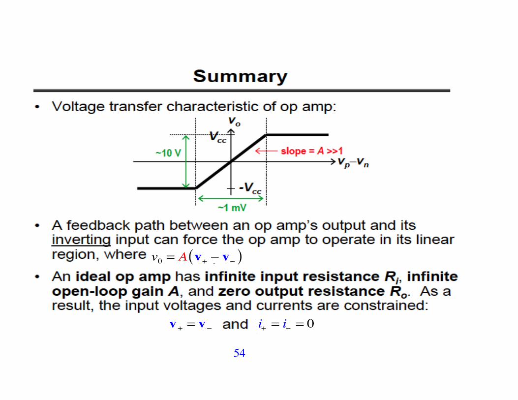
The voltage transfer characteristic of an op amp
v+ ! v!
v0
v0 =
!VCC if A v+ ! v!( ) < !VCC
A v+ ! v!( ) if !VCC!A v+ ! v!( ) "VCCVCC if VCC < A v+ ! v!( )
#
$%%
&%%
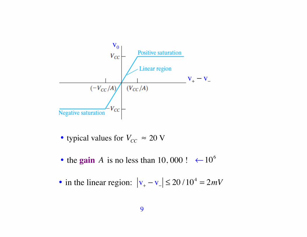
9
v+ ! v!
v0
• typical values for VCC ! 20 V
• the gain A is no less than 10, 000 ! !106
• in the linear region: v+ ! v! " 20 /104 = 2mV
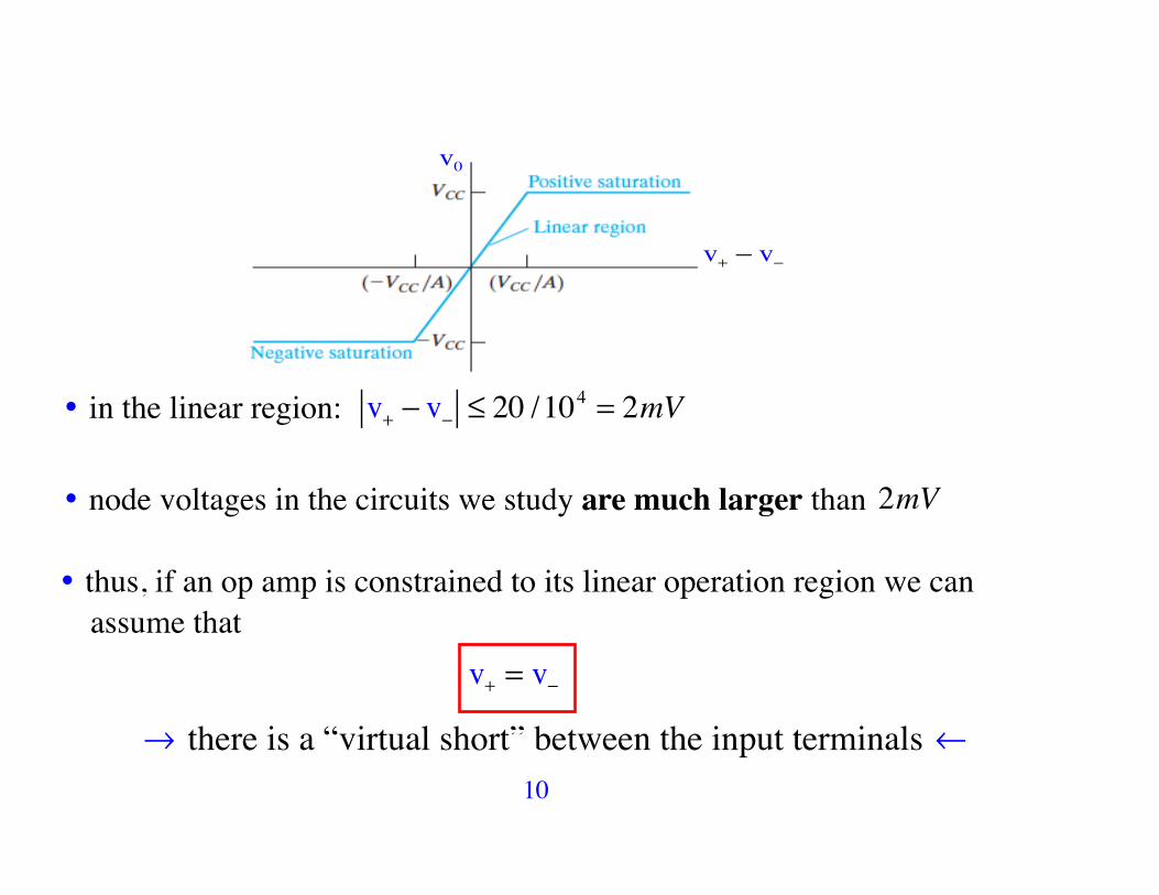
10
v+ ! v!
v0
• in the linear region: v+ ! v! " 20 /104 = 2mV
• node voltages in the circuits we study are much larger than 2mV
• thus, if an op amp is constrained to its linear operation region we can assume that
v+ = v! ! there is a “virtual short” between the input terminals !
11
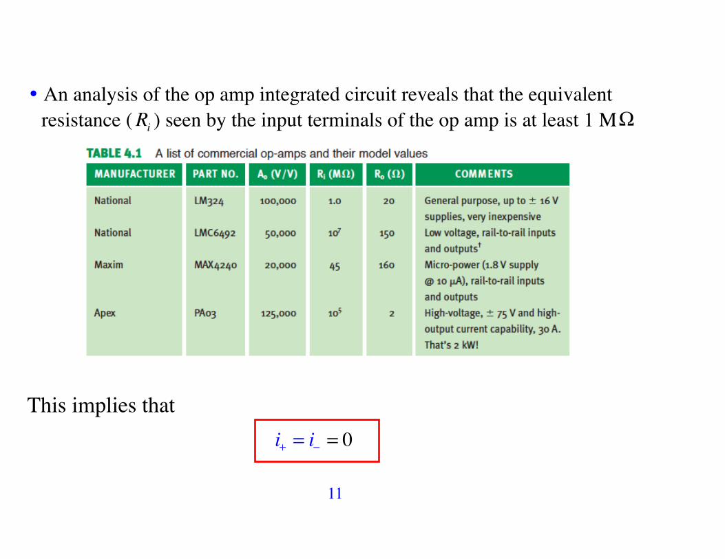
• An analysis of the op amp integrated circuit reveals that the equivalent resistance (Ri ) seen by the input terminals of the op amp is at least 1 M!
This implies that
i+ = i! = 0
12
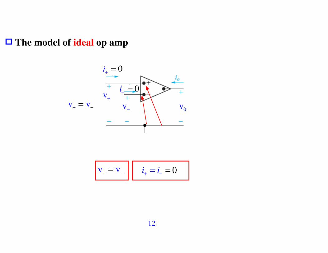
The model of ideal op amp
i+ = 0
i! = 0
v!v+ = v!v+
v0
v+ = v! i+ = i! = 0
13
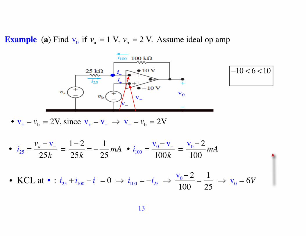
!10 < 6 <10
Example (a) Find v0 if va = 1 V, vb = 2 V. Assume ideal op amp
v+v!
i+i!
v0
•
• v+ = vb = 2V, since v+ = v! ! v! = vb = 2V
• i25 =va ! v!25k
= 1! 225k
= ! 125mA • i100 =
v0! v!100k
= v0! 2100
mA
• KCL at • : i25 + i100 ! i! = 0 ! i100 = !i25 ! v0! 2100
= 125
! v0 = 6V
!10 < 6 <10
14
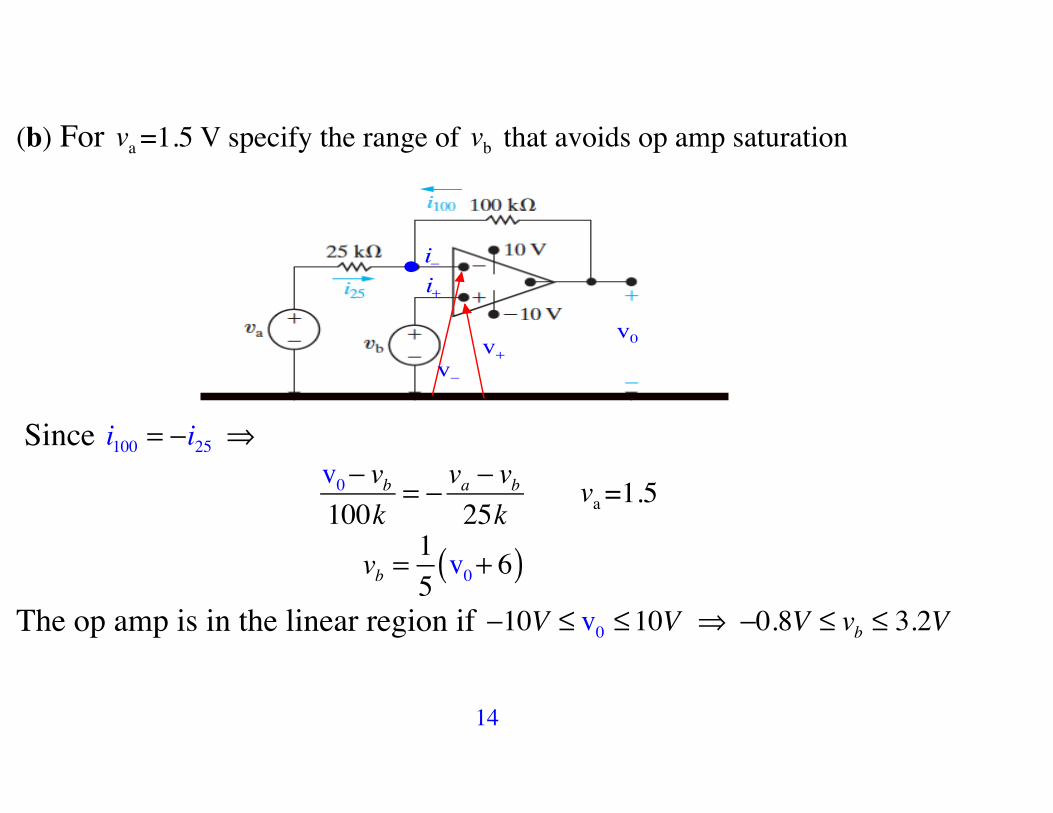
(b) For va=1.5 V specify the range of vb that avoids op amp saturation
v+
v!
i+i!
v0
•
Since i100 = !i25 !
v0! vb100k
= ! va ! vb25k
va=1.5
vb =15v0+ 6( )
The op amp is in the linear region if !10V " v0 "10V ! !0.8V " vb " 3.2V
15
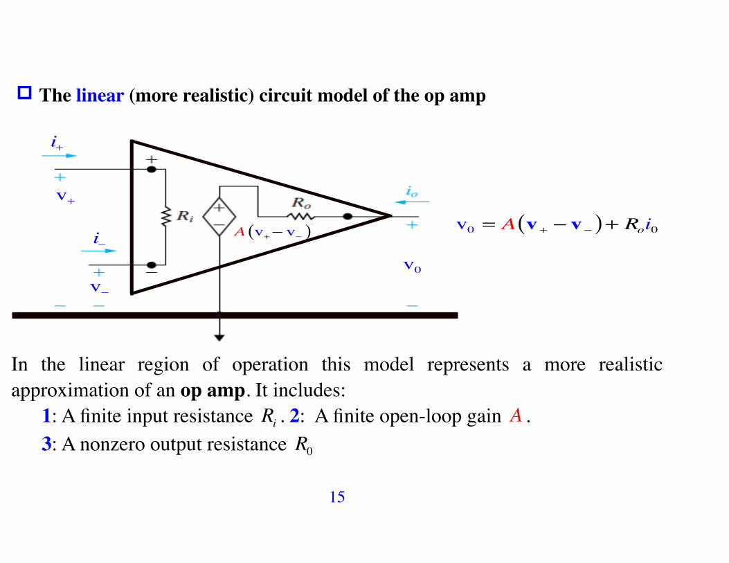
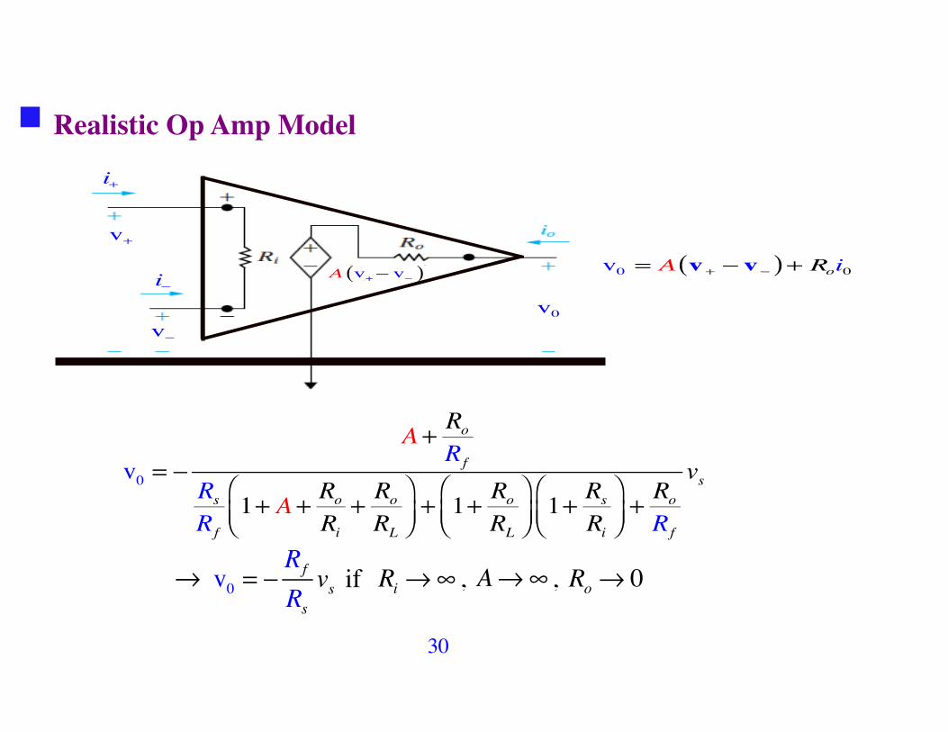
The linear (more realistic) circuit model of the op amp
i+
i!
v+
v!
A v+! v!( )
v0
v0 = A v+ ! v!( )+ Roi0
In the linear region of operation this model represents a more realistic approximation of an op amp. It includes: 1: A finite input resistance Ri . 2: A finite open-loop gain A . 3: A nonzero output resistance R0
16
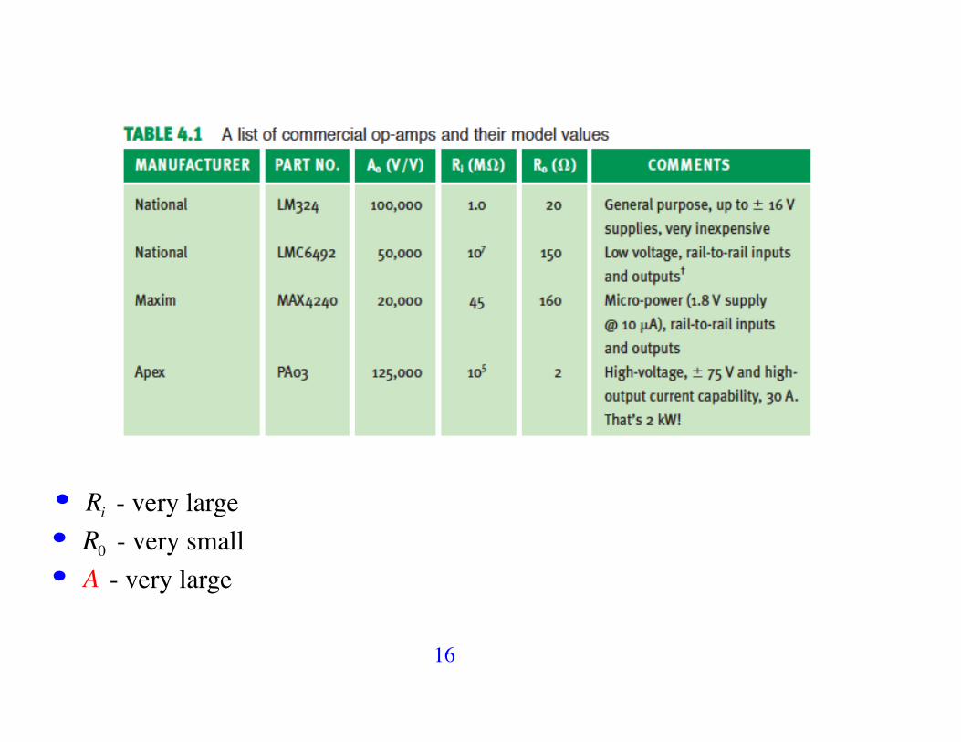
• Ri - very large • R0 - very small • A - very large
17
4.4 Negative Feedback
How does a circuit maintain a virtual short (v+ = v! ) at the input of an op amp, to ensure operation in the linear region ?
Negative feedback
The portion of the output voltage is applied to the inverting input, causing v+ ! v! to decrease and hence Vo to decrease, until the op amp operates in its linear region.
Positive feedback: the output quickly becomes saturated, i.e., Vo is stuck at one extreme or the other ( ±VCC ) and does not respond to the input.
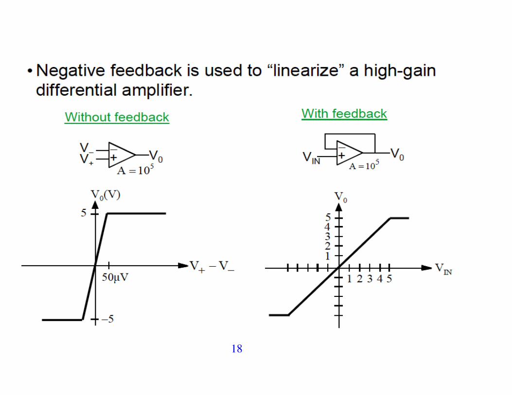
18
19
v0 =VS
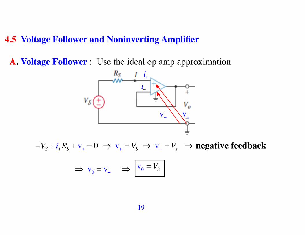
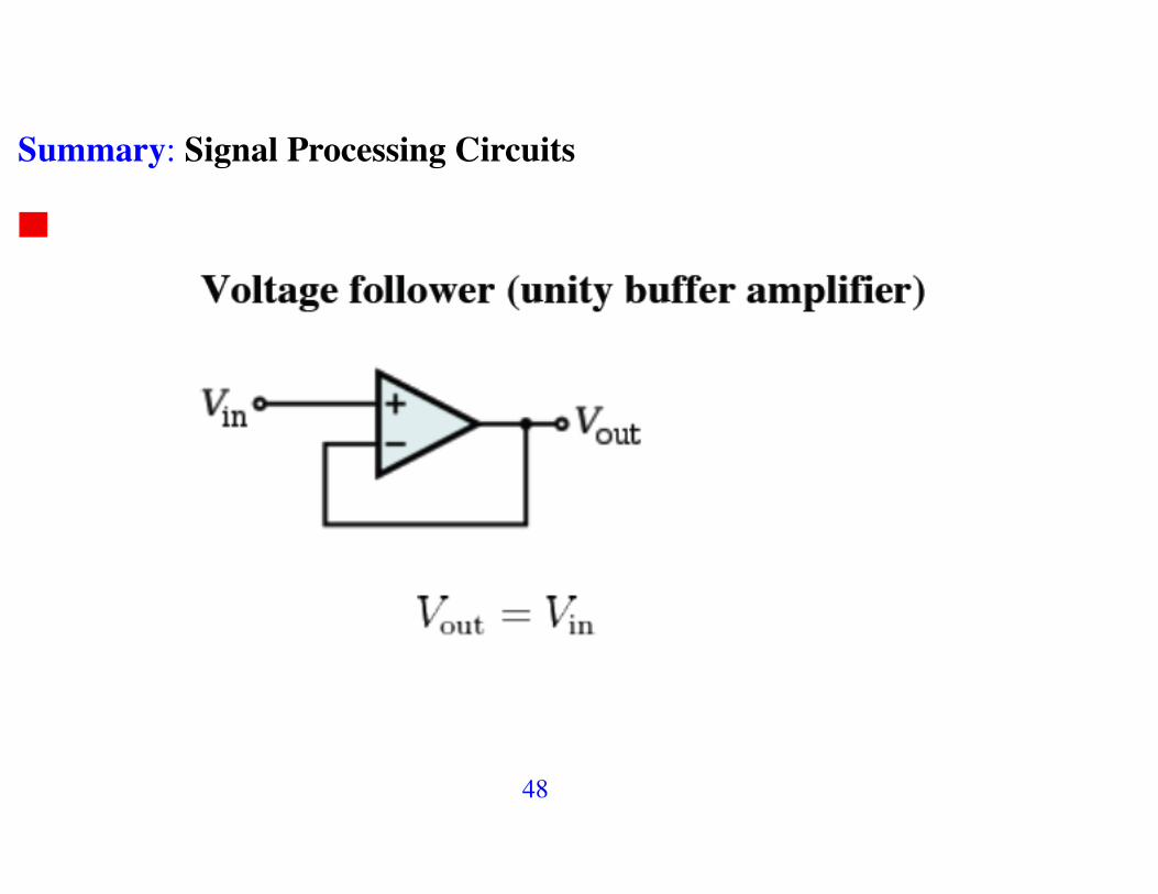
4.5 Voltage Follower and Noninverting Amplifier
A. Voltage Follower : Use the ideal op amp approximation
v+v!
i!
i+
!VS + i+RS + v+ = 0 ! v+ =VS ! v! =Vs ! negative feedback
! v0 = v! !
v0 =VS
20
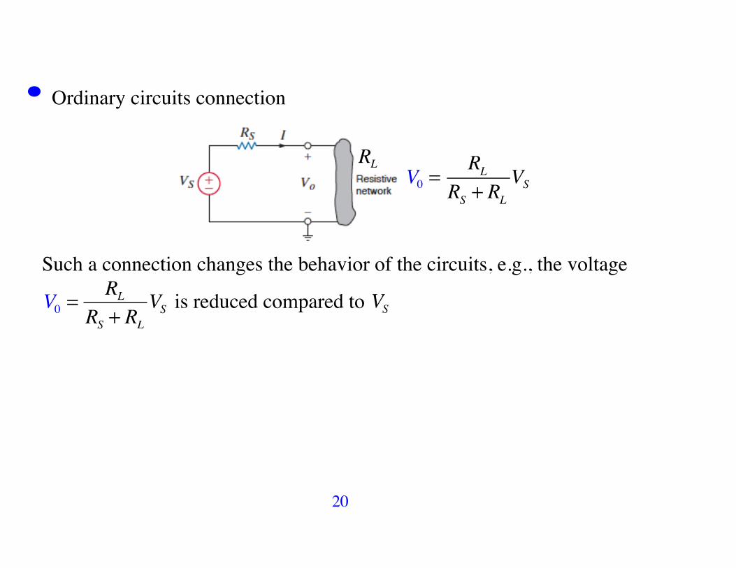
• Ordinary circuits connection
RLV0 =
RLRS + RL
VS
Such a connection changes the behavior of the circuits, e.g., the voltage
V0 =RL
RS + RL
VS is reduced compared to VS
21
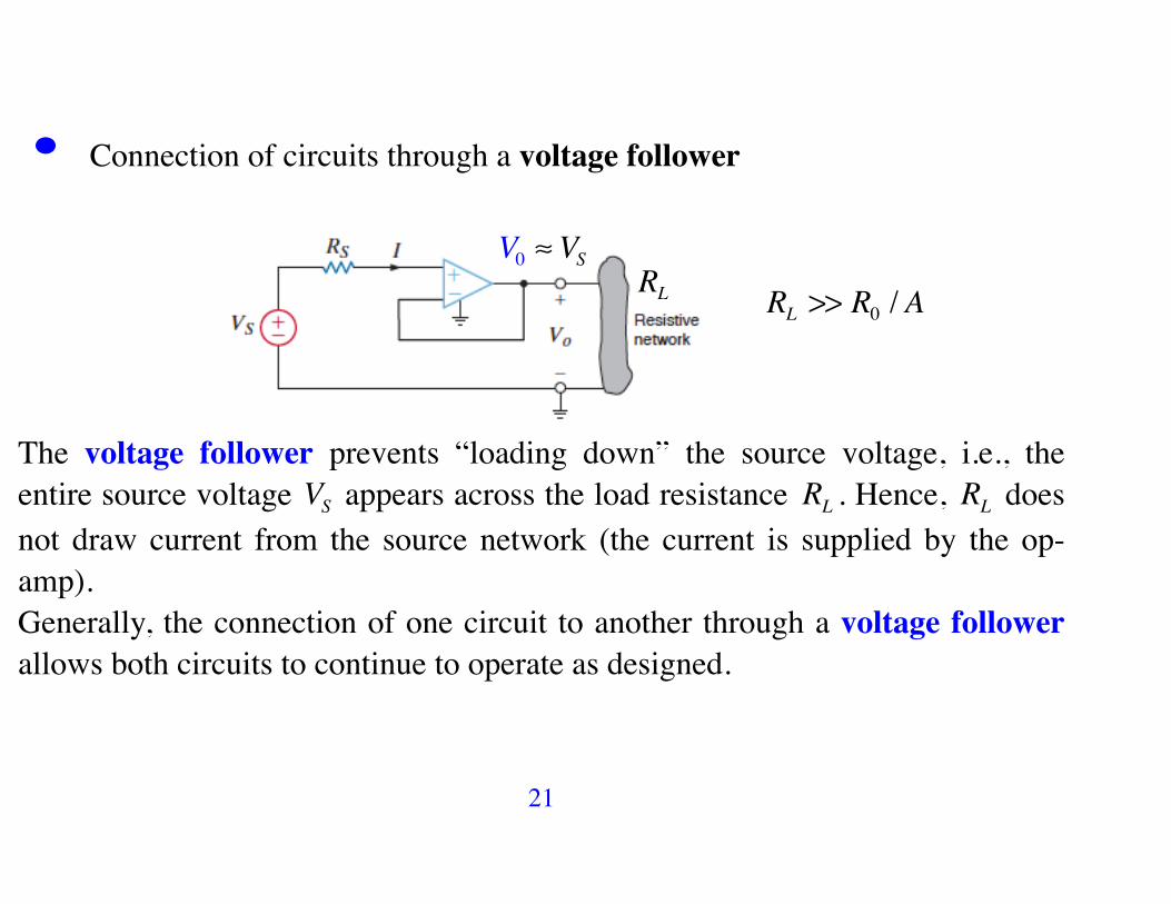
• Connection of circuits through a voltage follower
RLV0 !VS
RL >> R0 /A
The voltage follower prevents “loading down” the source voltage, i.e., the entire source voltage VS appears across the load resistance RL . Hence, RL does not draw current from the source network (the current is supplied by the op-amp).Generally, the connection of one circuit to another through a voltage follower allows both circuits to continue to operate as designed.
22
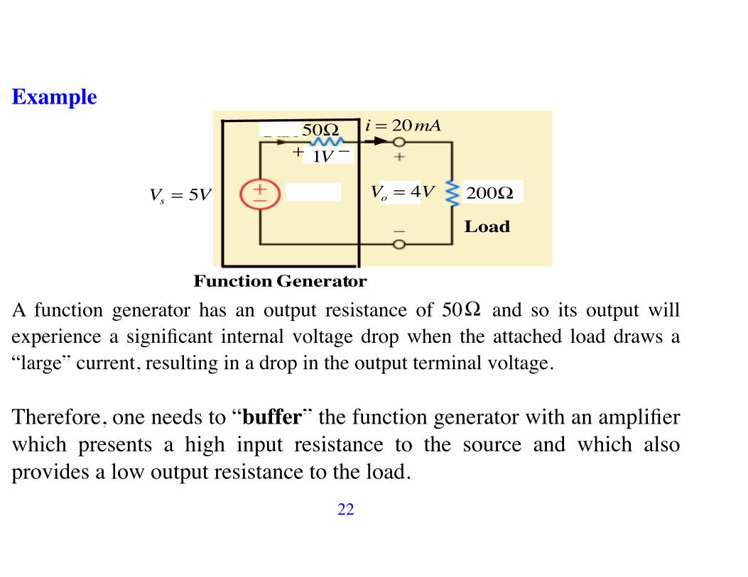
Example
Vs = 5V
50! i = 20mA
200!
Function Generator
Load
+ "1V
Vo = 4V 200!
A function generator has an output resistance of 50! and so its output will experience a significant internal voltage drop when the attached load draws a “large” current, resulting in a drop in the output terminal voltage.
Therefore, one needs to “buffer” the function generator with an amplifier which presents a high input resistance to the source and which also provides a low output resistance to the load.
23
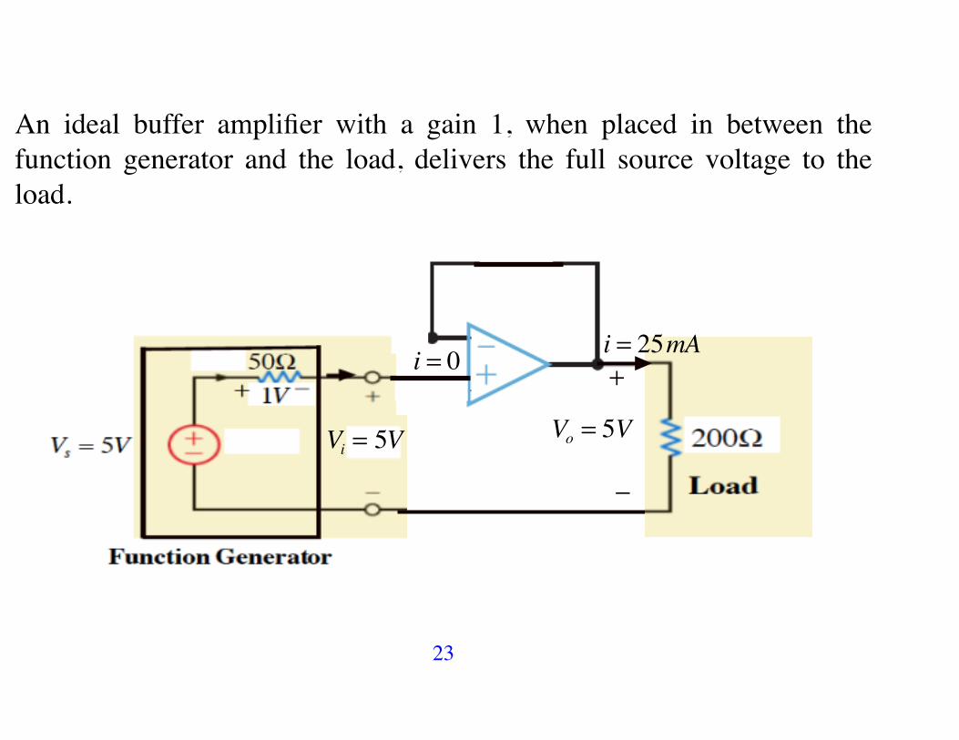
An ideal buffer amplifier with a gain 1, when placed in between the function generator and the load, delivers the full source voltage to the load.
i = 0
Vi = 5V
i = 25mA
Vo = 5V
+
!
24
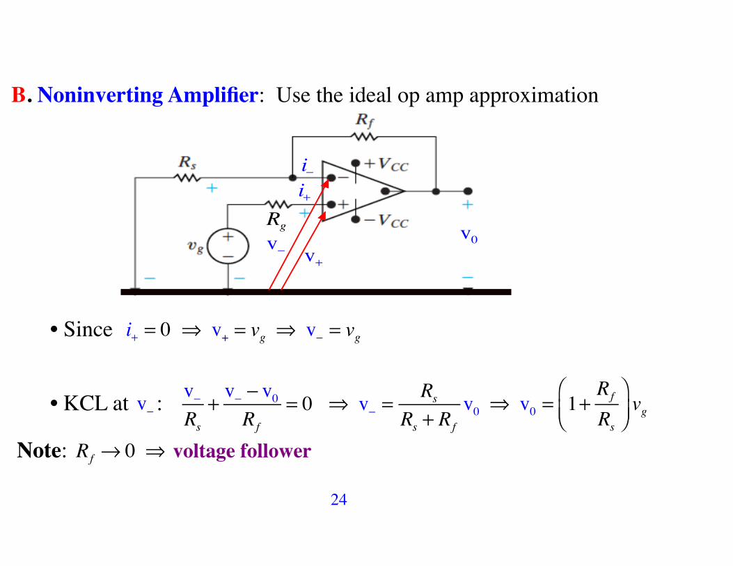
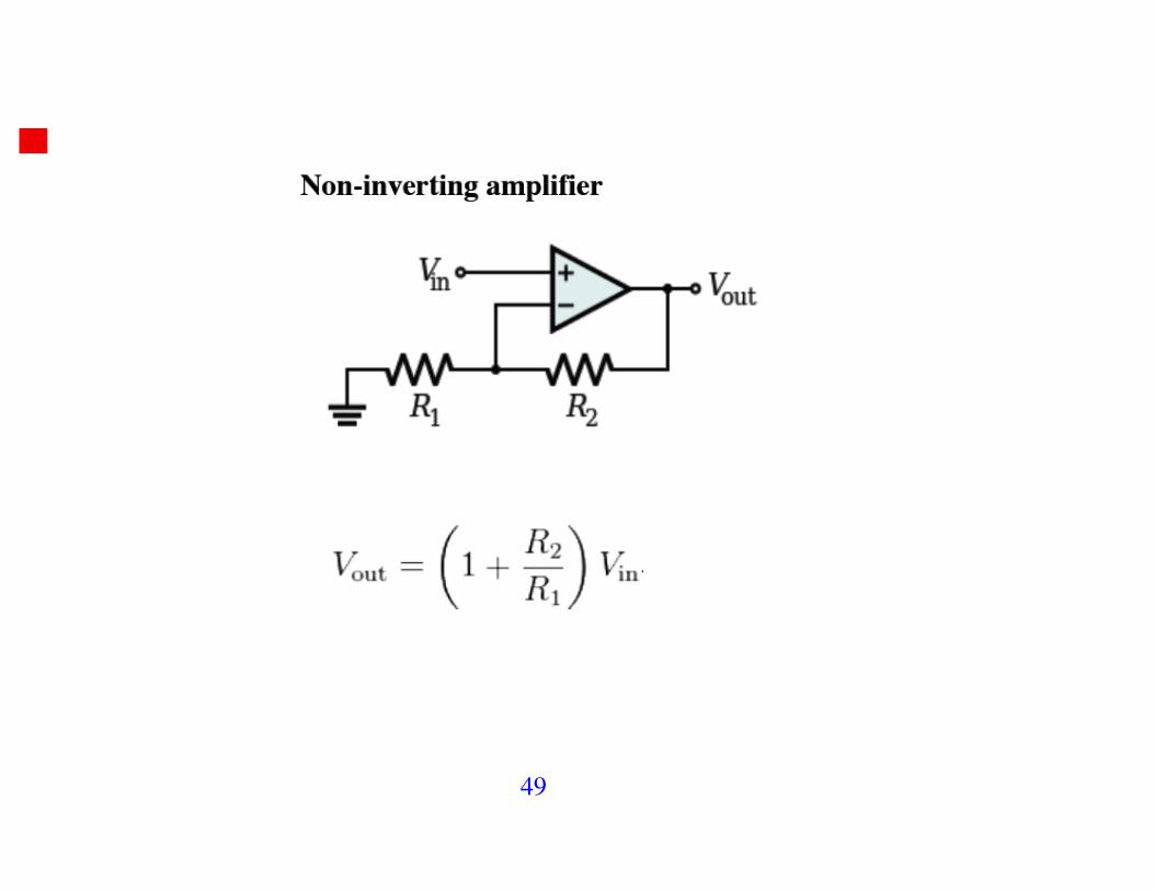
B. Noninverting Amplifier: Use the ideal op amp approximation
i!i+
v+v!
v0Rg
• Since i+ = 0 ! v+ = vg ! v! = vg
• KCL at v! : v!Rs
+ v! ! v0Rf
= 0 ! v! =Rs
Rs + Rf
v0 ! v0 = 1+Rf
Rs
!"#
$%&vg
Note: Rf ! 0 ! voltage follower
25
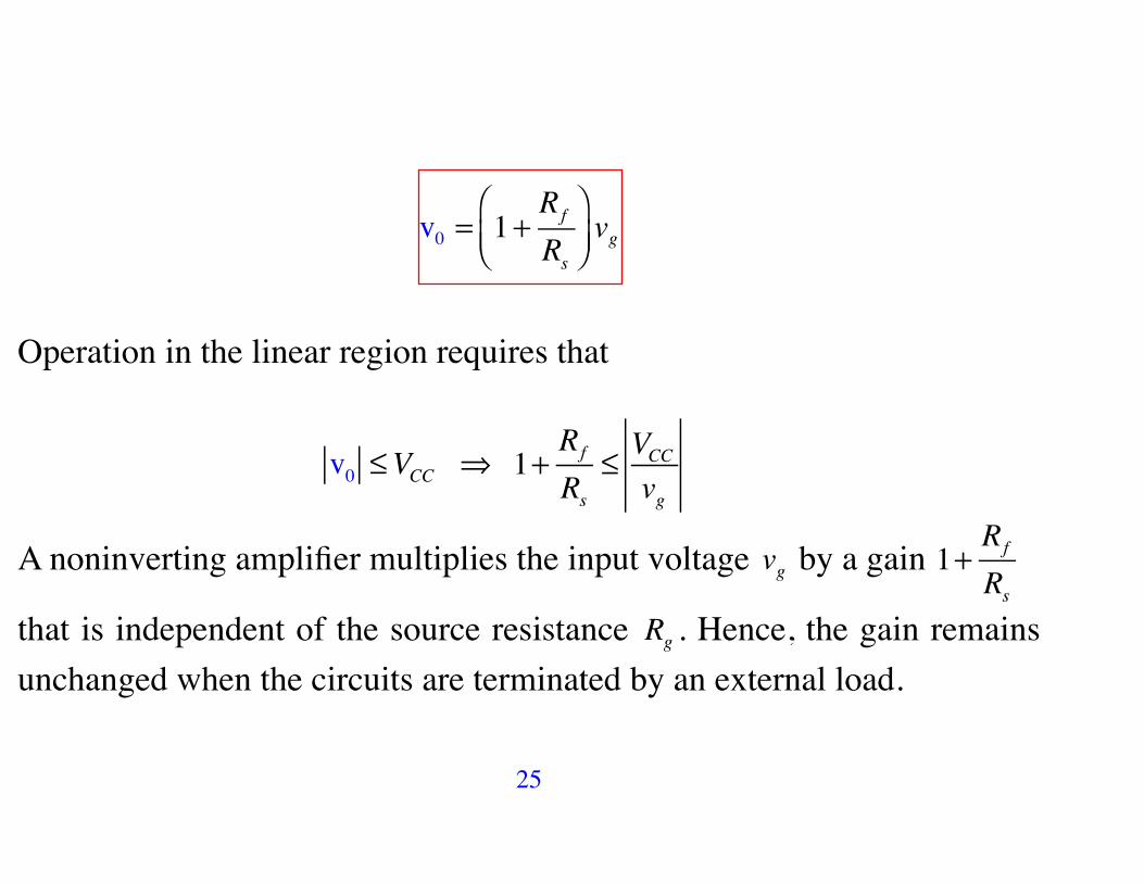
v0 = 1+Rf
Rs
!"#
$%&vg
Operation in the linear region requires that
v0 !VCC ! 1+Rf
Rs! VCC
vg
A noninverting amplifier multiplies the input voltage vg by a gain 1+Rf
Rs
that is independent of the source resistance Rg . Hence, the gain remains unchanged when the circuits are terminated by an external load.
26
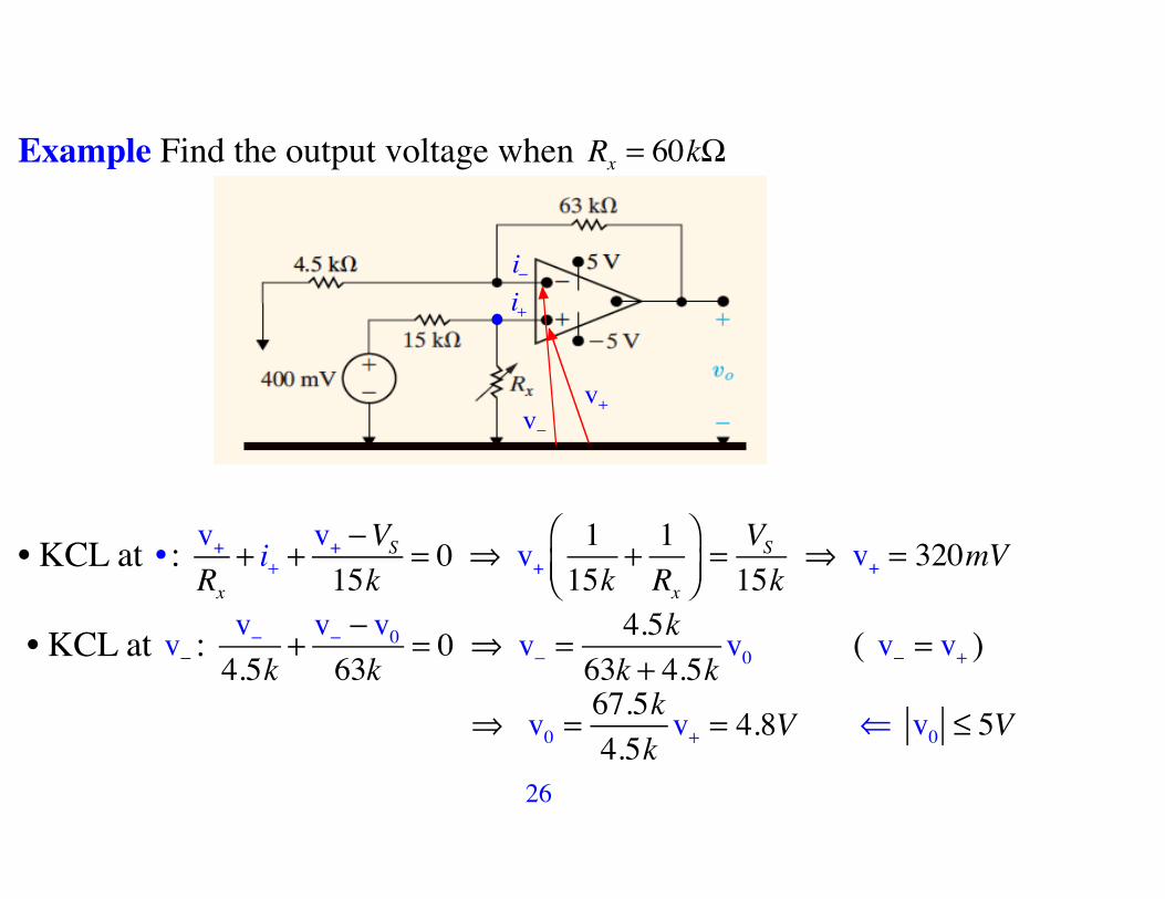
Example Find the output voltage when Rx = 60k!
v!
i!i+
v+v!
•
• KCL at • : v+Rx
+ i+ +v+ !VS15k
= 0 ! v+115k
+ 1Rx
!"#
$%&= VS15k
! v+ = 320mV
• KCL at v! : v!4.5k
+ v! ! v063k
= 0 ! v! =4.5k
63k + 4.5kv0 ( v! = v+ )
! v0 =67.5k4.5k
v+ = 4.8V ! v0 ! 5V
27
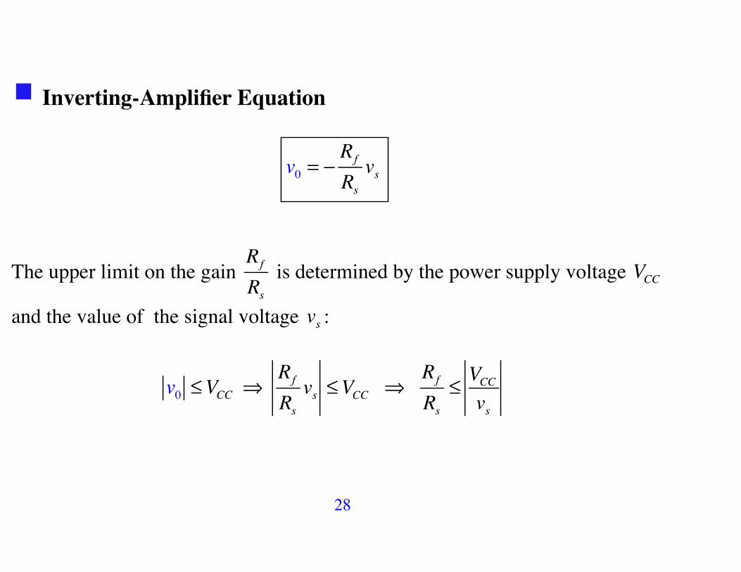
v0 = !Rf
Rsvs
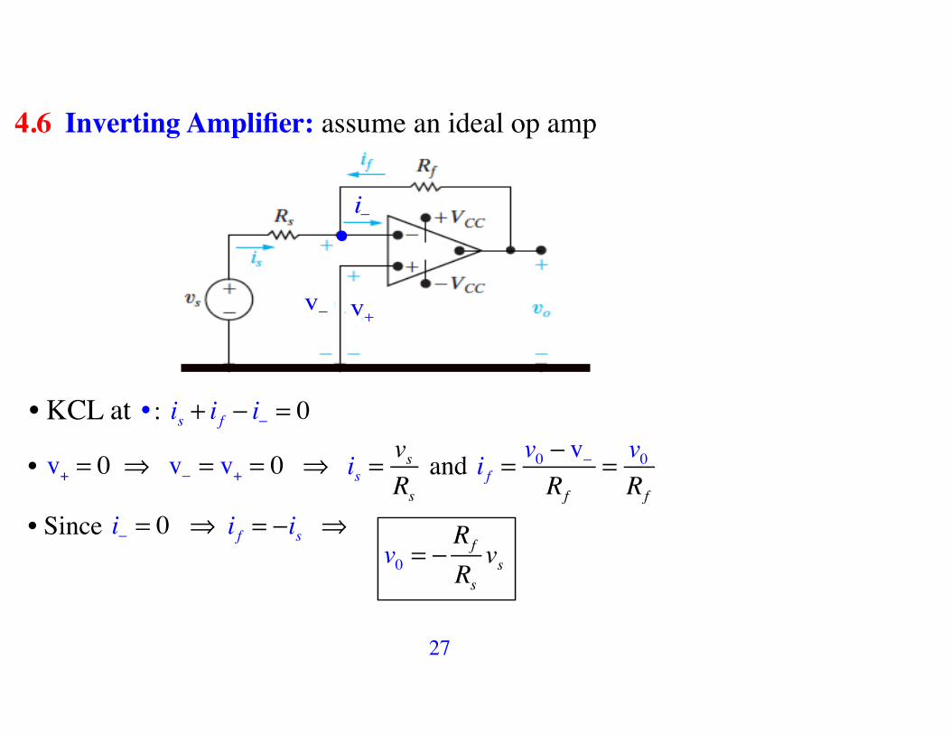
4.6 Inverting Amplifier: assume an ideal op amp
i!
v! v+
•
• KCL at • : is + i f ! i! = 0
• v+ = 0 ! v! = v+ = 0 ! is =vsRs
and i f =v0 ! v!Rf
= v0Rf
• Since i! = 0 ! i f = !is ! v0 = !
Rf
Rsvs
28
v0 = !Rf
Rsvs
Inverting-Amplifier Equation
The upper limit on the gain Rf
Rs is determined by the power supply voltage VCC
and the value of the signal voltage vs :
v0 !VCC ! Rf
Rsvs !VCC !
Rf
Rs! VCC
vs
v0 = !Rf
Rsvs
29
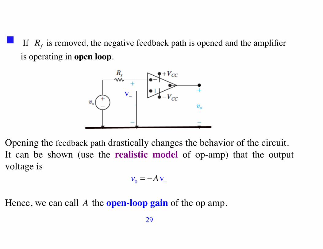
If Rf is removed, the negative feedback path is opened and the amplifier is operating in open loop.
v!
Opening the feedback path drastically changes the behavior of the circuit. It can be shown (use the realistic model of op-amp) that the output voltage is v0 = !Av!
Hence, we can call A the open-loop gain of the op amp.
30
Realistic Op Amp Model
i+
i!
v+
v!
A v+! v!( )
v0
v0 = A v+ ! v!( )+ Roi0
v0 = !A + Ro
Rf
RsRf
1+ A + RoRi
+ RoRL
"#$
%&'+ 1+ Ro
RL
"#$
%&'1+ Rs
Ri
"#$
%&'+ RoRf
vs
! v0 = !Rf
Rsvs if Ri !" , A!" , Ro ! 0
31
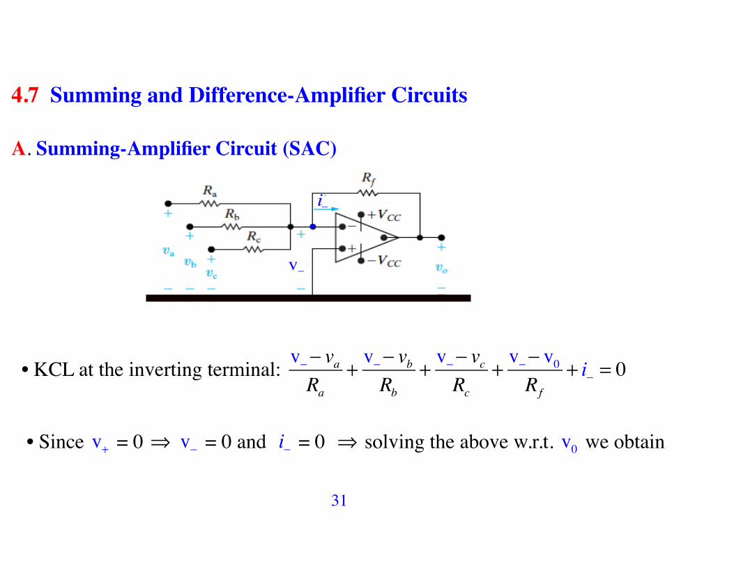
4.7 Summing and Difference-Amplifier Circuits
A. Summing-Amplifier Circuit (SAC)
v!
i!•
• KCL at the inverting terminal: v! ! vaRa
+ v! ! vbRb
+ v! ! vcRc
+ v! ! v0Rf
+ i! = 0
• Since v+ = 0 ! v! = 0 and i! = 0 ! solving the above w.r.t. v0 we obtain
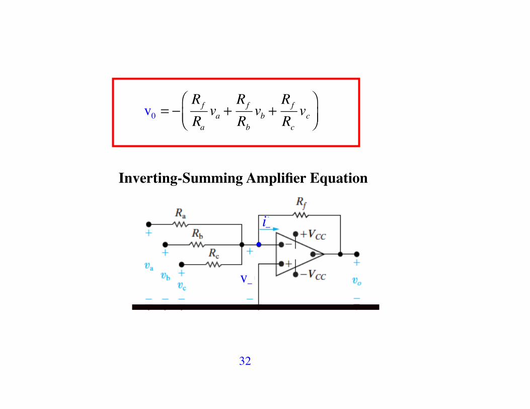
32
v0 = !
Rf
Rava +
Rf
Rbvb +
Rf
Rcvc
"#$
%&'
Inverting-Summing Amplifier Equation
v!
i!•
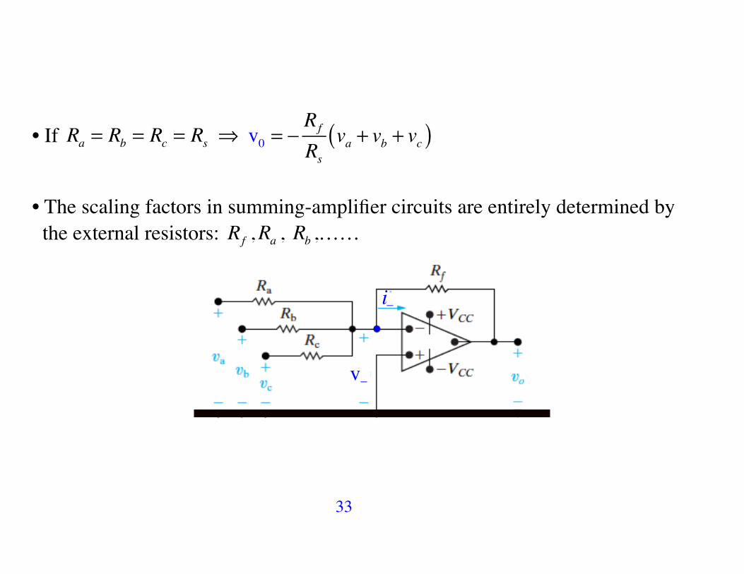
33
• If Ra = Rb = Rc = Rs ! v0 = !Rf
Rsva + vb + vc( )
• The scaling factors in summing-amplifier circuits are entirely determined by the external resistors: Rf ,Ra , Rb ,……
v!
i!•
34
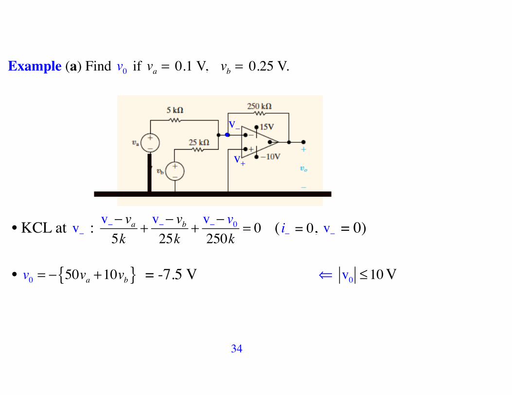
Example (a) Find v0 if va = 0.1 V, vb = 0.25 V.
v+
v!•
• KCL at v! : v! ! va5k
+ v! ! vb25k
+ v! ! v0250k
= 0 ( i! = 0, v! = 0)
• v0 = ! 50va +10vb{ } = -7.5 V ! v0 !10V
35
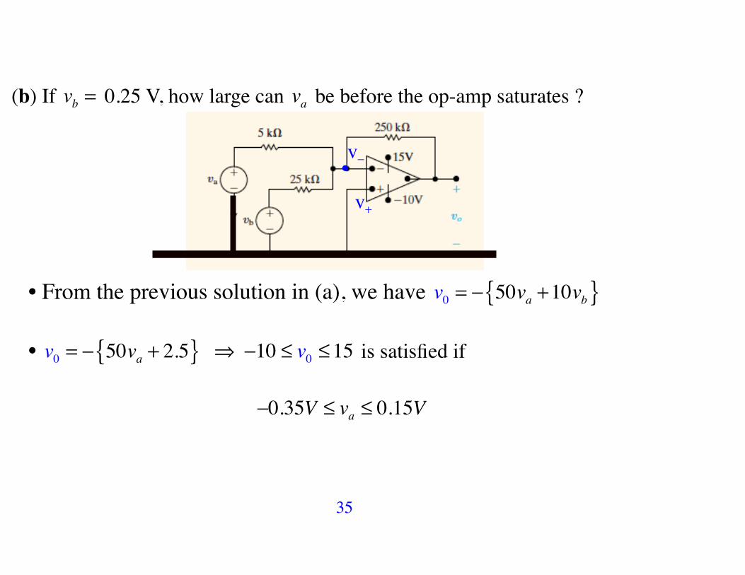
(b) If vb = 0.25 V, how large can va be before the op-amp saturates ?
v+
v!•
• From the previous solution in (a), we have v0 = ! 50va +10vb{ }
• v0 = ! 50va + 2.5{ } ! !10 " v0 "15 is satisfied if
!0.35V " va " 0.15V
36
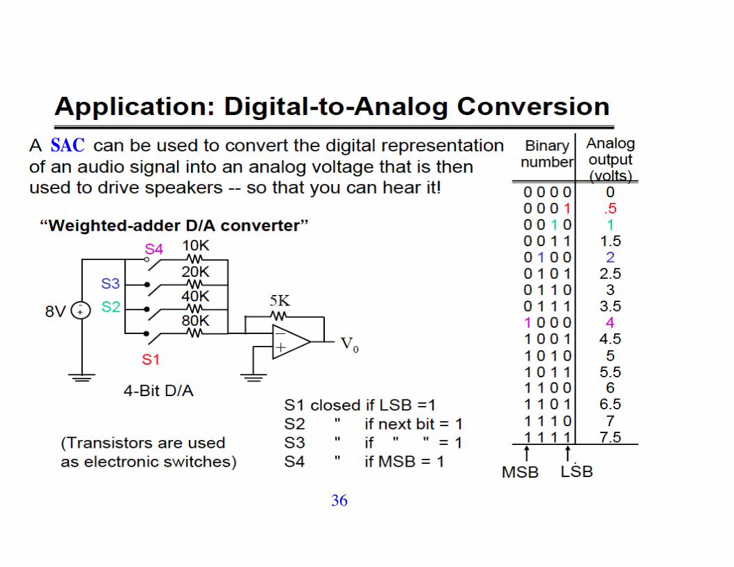
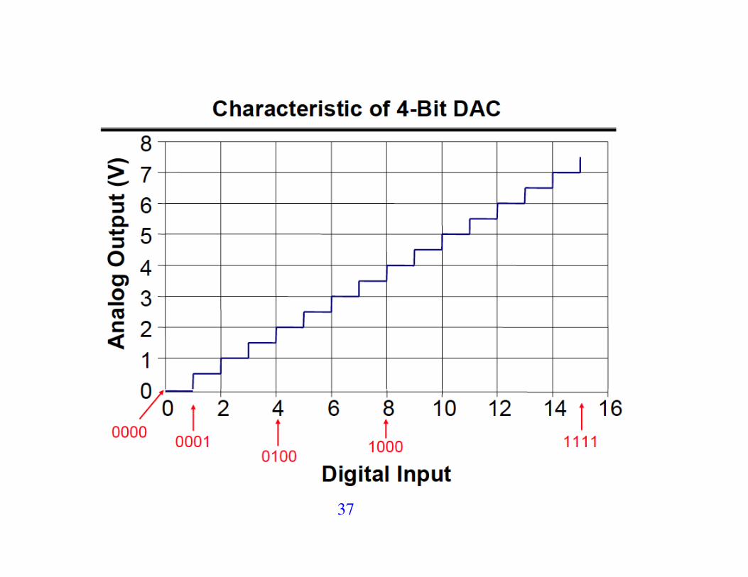
SAC
37
38
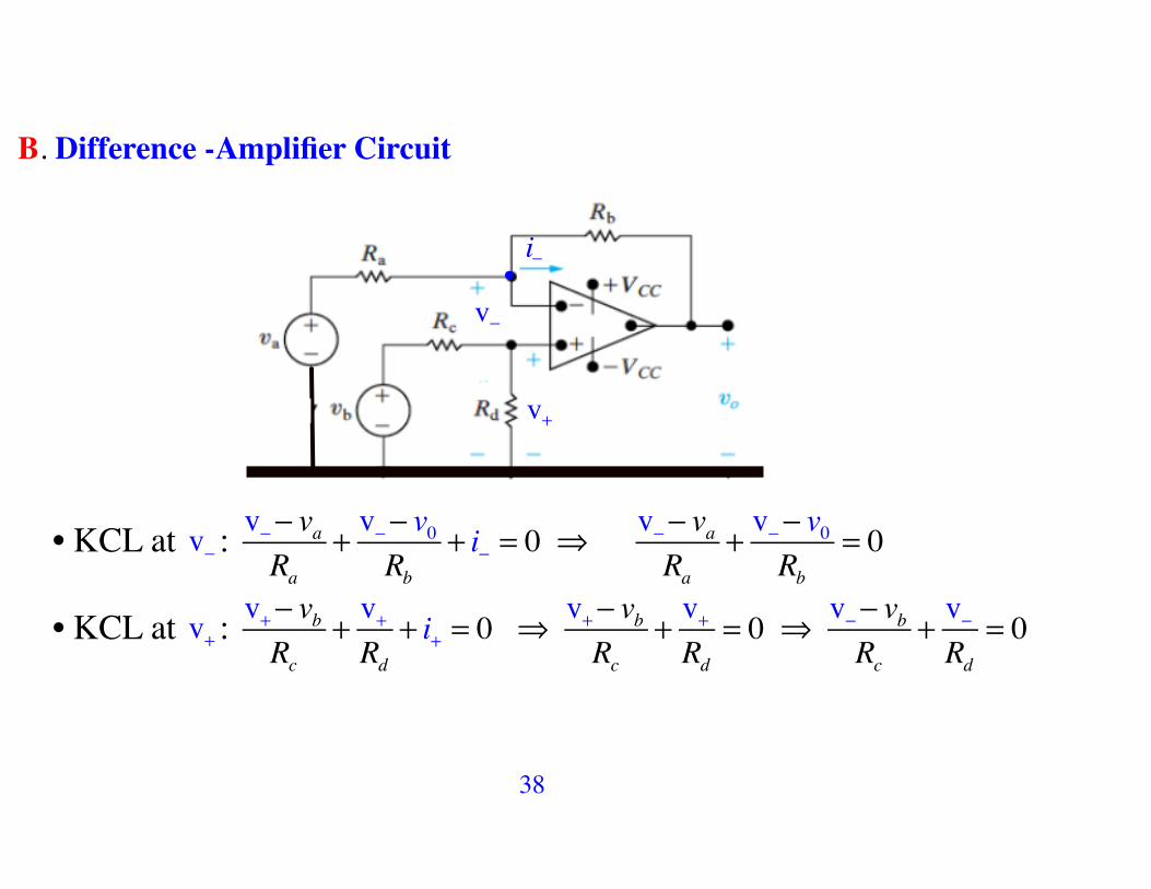
B. Difference -Amplifier Circuit
v!
v+
i!•
• KCL at v! : v! ! vaRa
+ v! ! v0Rb
+ i! = 0 ! v! ! vaRa
+ v! ! v0Rb
= 0
• KCL at v+ : v+! vbRc
+ v+Rd
+ i+ = 0 ! v+! vbRc
+ v+Rd
= 0 ! v! ! vbRc
+ v!Rd
= 0
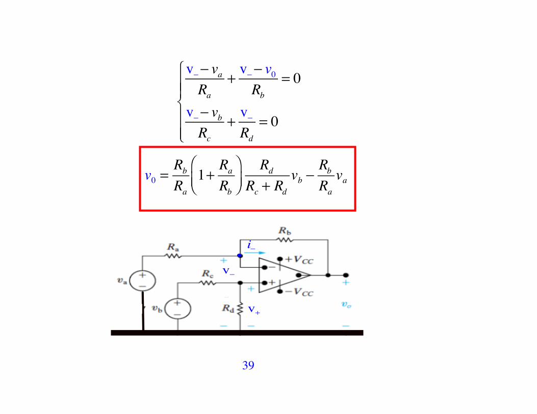
39
v! ! vaRa
+ v! ! v0Rb
= 0
v! ! vbRc
+ v!Rd
= 0
"
#$$
%$$
v0 =
RbRa
1+RaRb
!"#
$%&
RdRc + Rd
vb 'RbRava
v!
v+
i!•
40
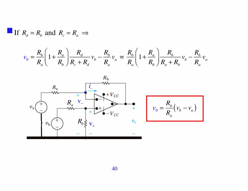
If Rd = Rb and Rc = Ra !
v0 =RbRa
1+ RaRb
!"#
$%&
RdRc + Rd
vb 'RbRava = Rb
Ra1+ Ra
Rb
!"#
$%&
RbRa + Rb
vb 'RbRava
v!
v+
i!•
Rb
Ra v0 =RbRa
vb ! va( )
41
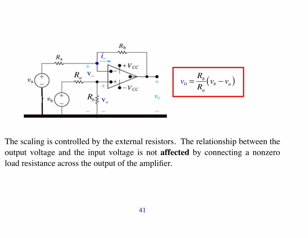
v!
v+
i!•
Rb
Ra v0 =RbRa
vb ! va( )
The scaling is controlled by the external resistors. The relationship between the output voltage and the input voltage is not affected by connecting a nonzero load resistance across the output of the amplifier.
42
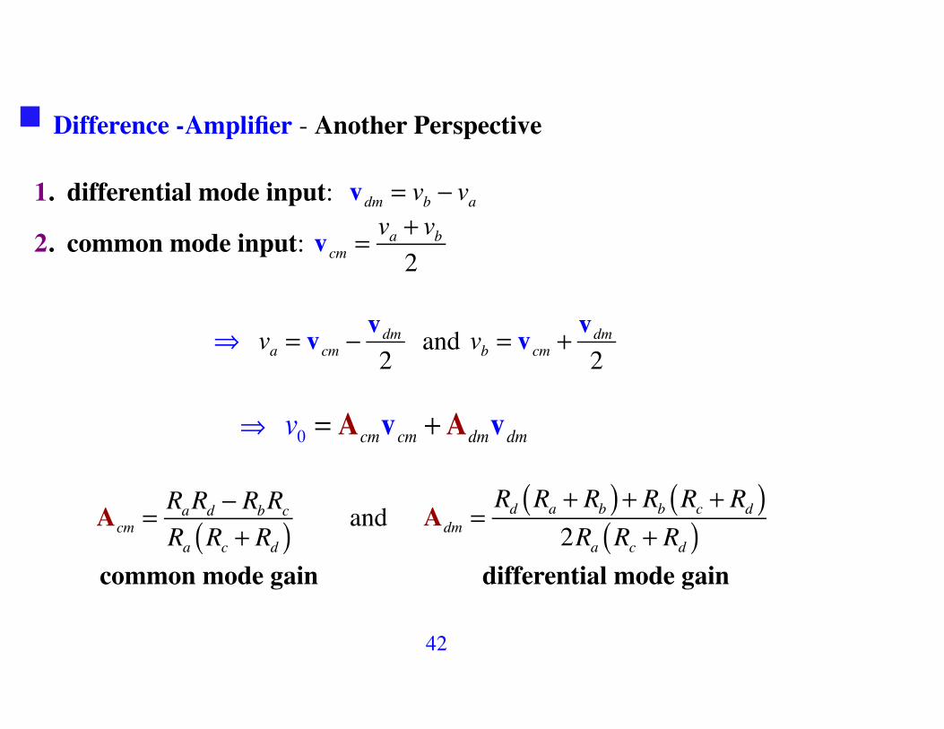
Difference -Amplifier - Another Perspective
1. differential mode input: vdm = vb ! va
2. common mode input: vcm = va + vb2
! va = vcm !vdm2
and vb = vcm +vdm2
! v0 = Acmvcm +Admvdm
Acm = RaRd ! RbRcRa Rc + Rd( ) and Adm =
Rd Ra + Rb( )+ Rb Rc + Rd( )2Ra Rc + Rd( )
common mode gain differential mode gain
43
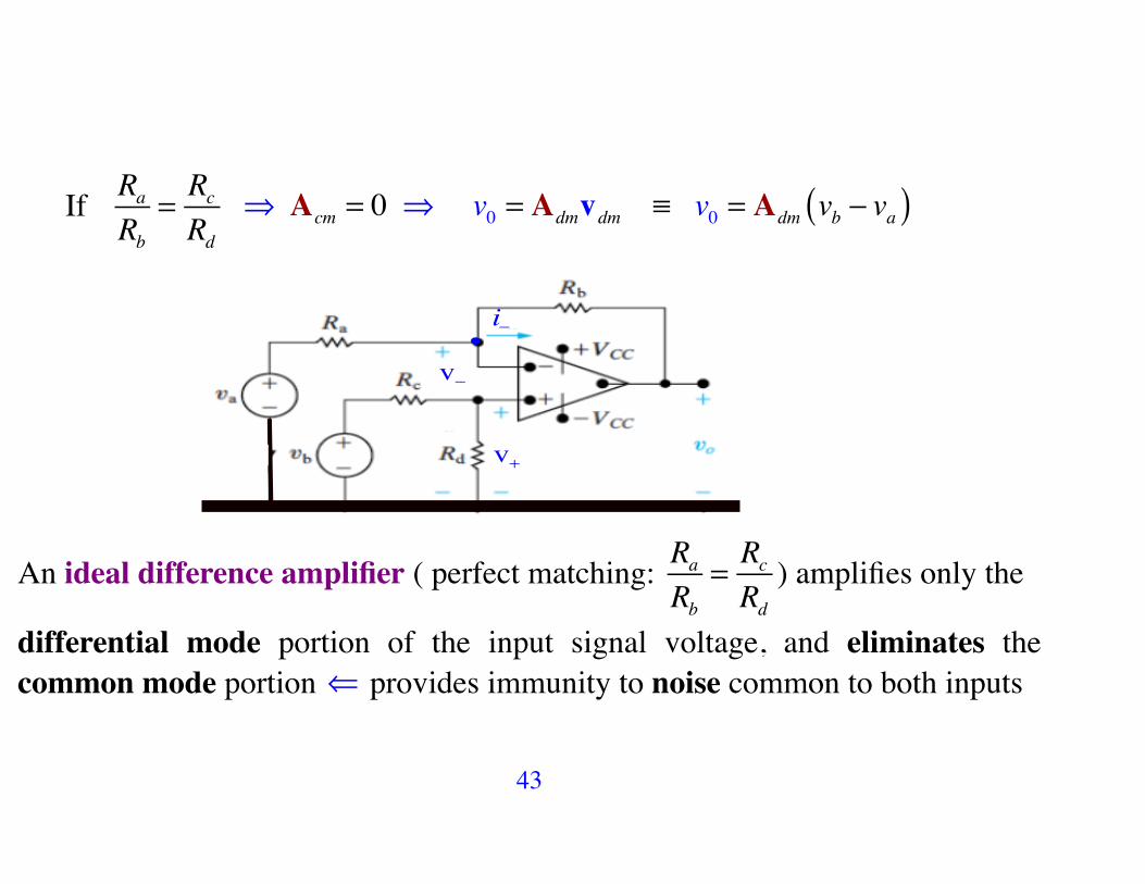
If RaRb
= RcRd
! Acm = 0 ! v0 = Admvdm ! v0 = Adm vb ! va( )
v!
v+
i!•
An ideal difference amplifier ( perfect matching: RaRb
= RcRd
) amplifies only the
differential mode portion of the input signal voltage, and eliminates the common mode portion ! provides immunity to noise common to both inputs
44
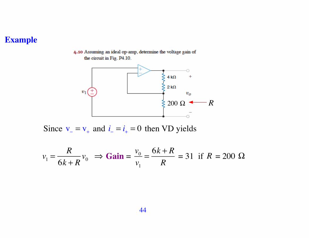
Example
200 ! R
Since v! = v+ and i! = i+ = 0 then VD yields
v1 =R
6k + Rv0 ! Gain = v0
v1= 6k + R
R = 31 if R = 200 !
45
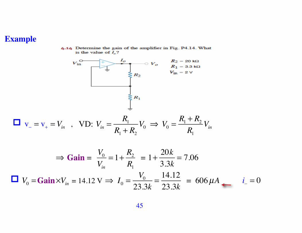
Example
v! = v+ =Vin , VD: Vin =R1
R1 + R2V0 ! V0 =
R1 + R2R1
Vin
! Gain = V0Vin
= 1+ R2R1
= 1+ 20k3.3k
= 7.06
V0 =Gain!Vin = 14.12 V ! I0 =V023.3k
= 14.1223.3k
= 606µA i! = 0
46
Example
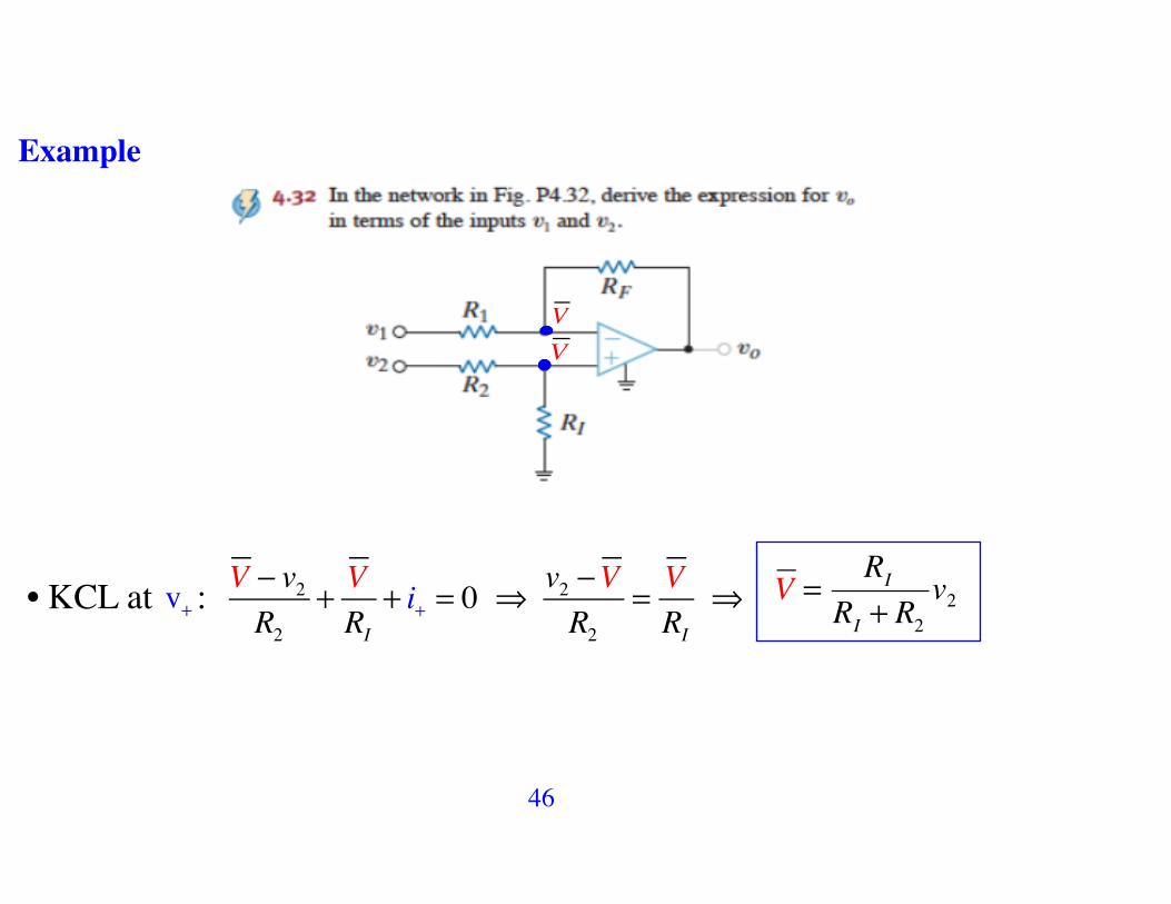
VV
• KCL at v+ : V ! v2R2
+ VRI
+ i+ = 0 ! v2 !VR2
= VRI
! V =RI
RI + R2v2
47
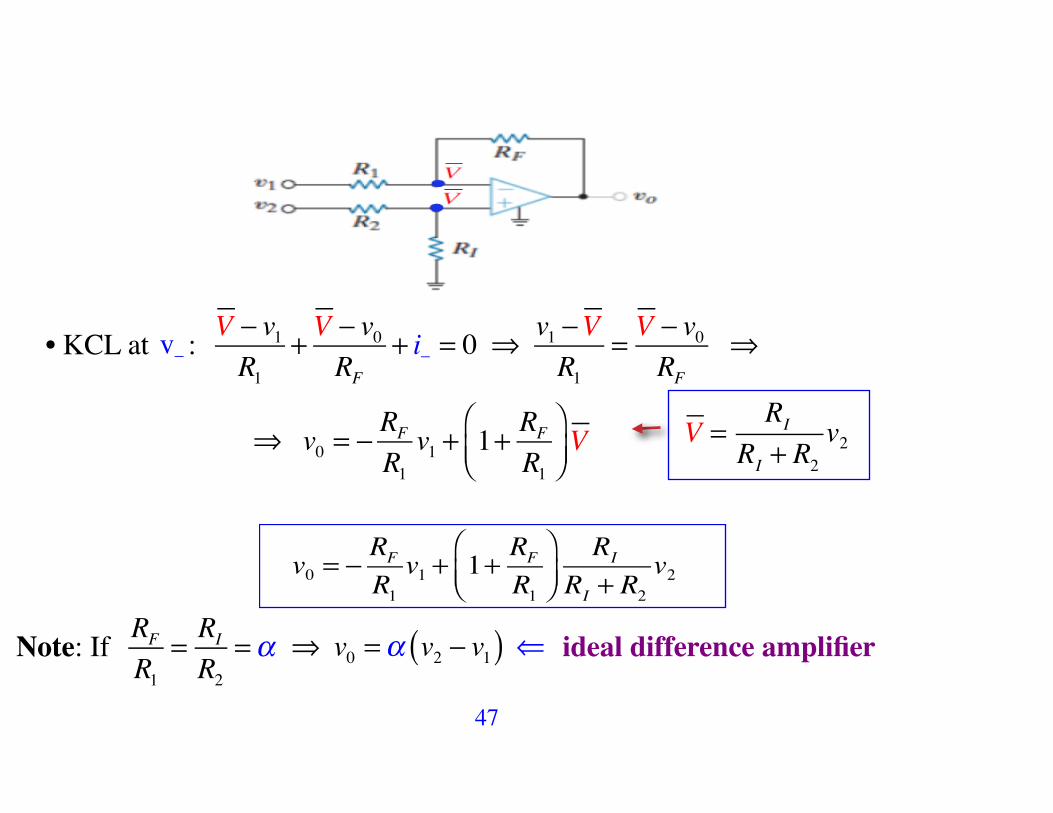
• KCL at v! : V ! v1R1
+ V ! v0RF
+ i! = 0 ! v1 !VR1
= V ! v0RF
!
! v0 = ! RFR1v1 + 1+ RF
R1
"#$
%&'V V =
RI
RI + R2v2
v0 = !RFR1v1 + 1+
RFR1
"#$
%&'
RI
RI + R2v2
Note: If RFR1
= RI
R2=! ! v0 =! v2 " v1( ) ! ideal difference amplifier
48
Summary: Signal Processing Circuits
49
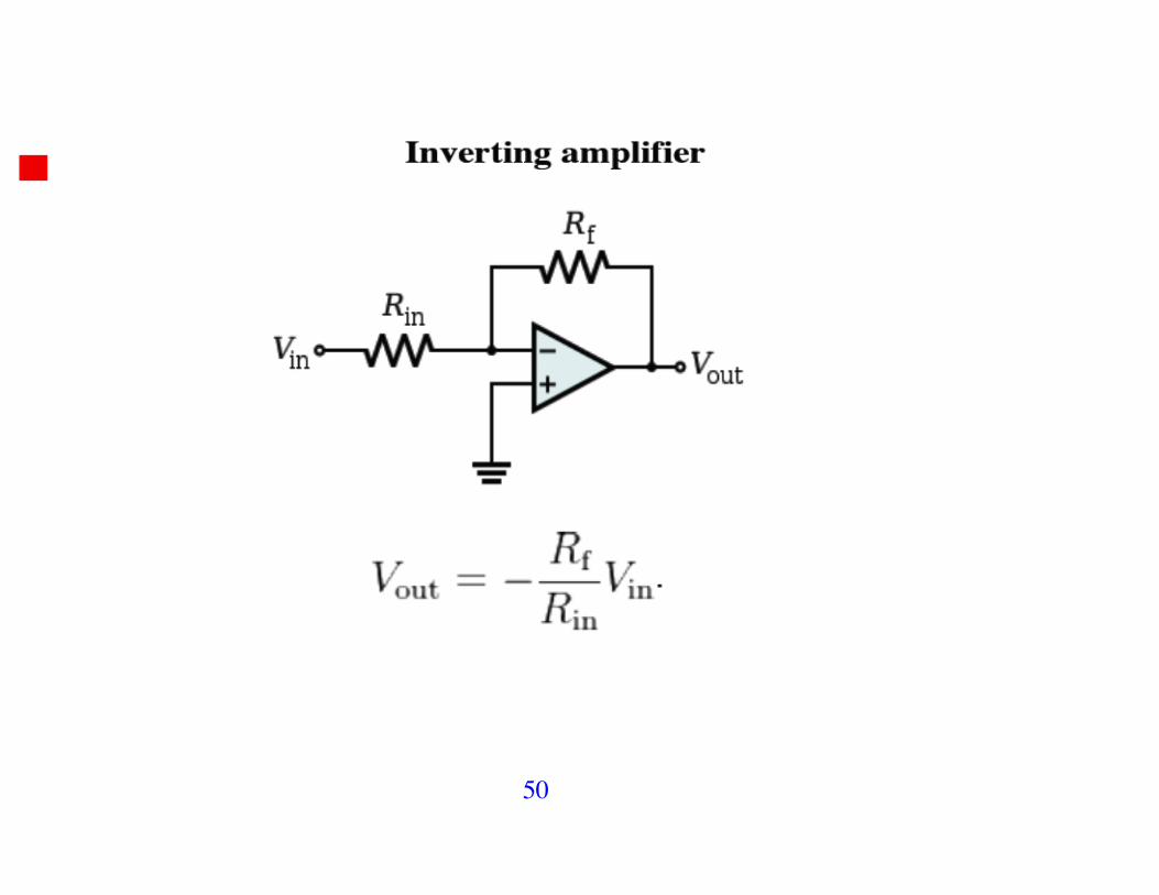
50
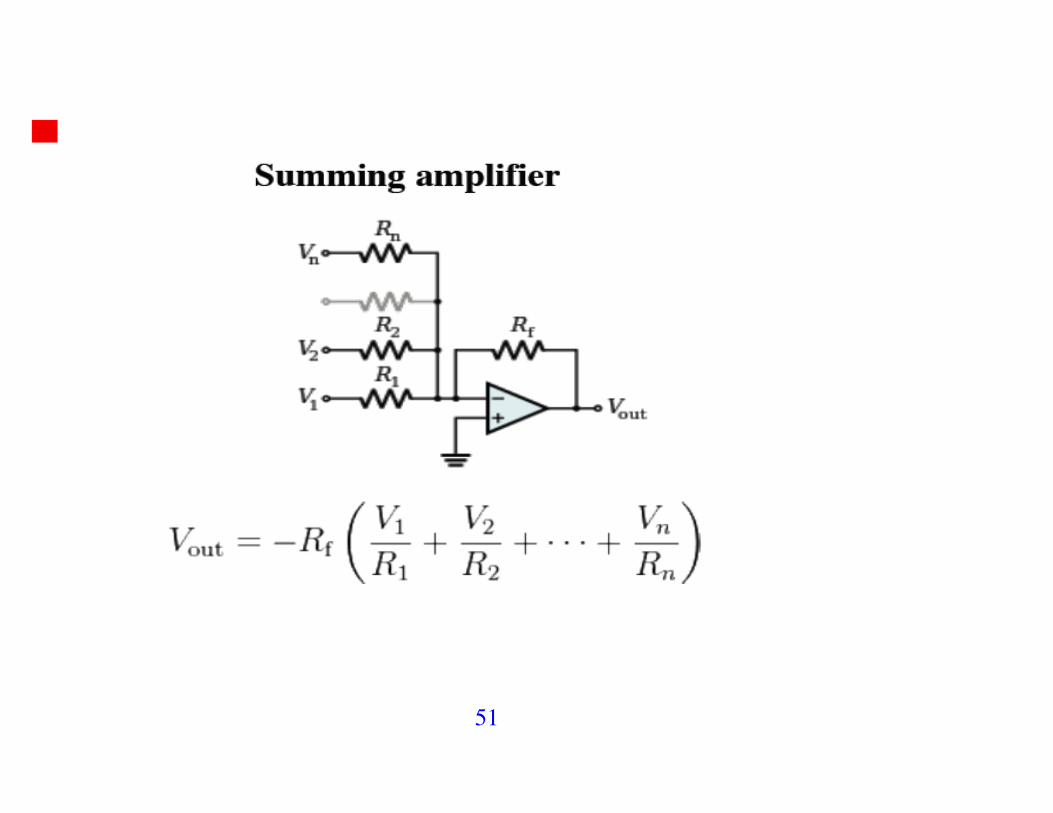
51
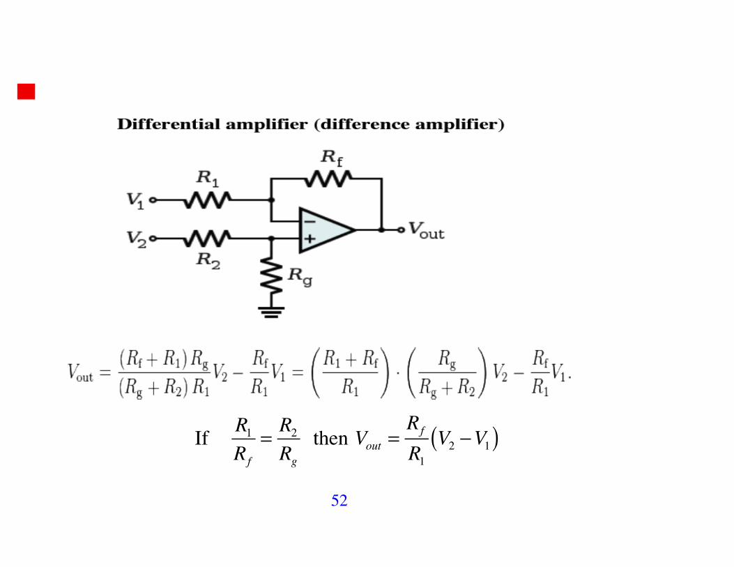
52
If R1Rf
= R2Rg
then Vout =Rf
R1V2 !V1( )
53
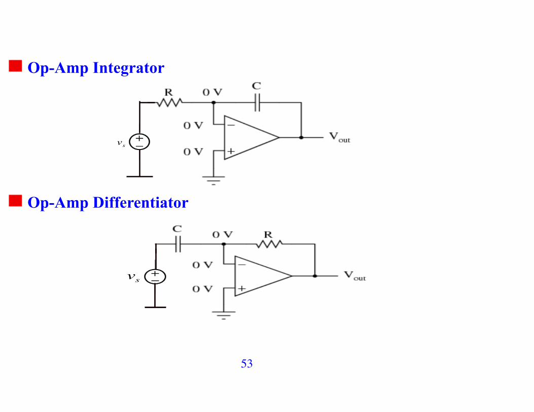
Op-Amp Integrator
vs
Op-Amp Differentiator
vs
54
v0 = A v+ ! v!( )
v+ = v! i+ = i! = 0
55
4.8 Problems ! Set 4


![The Operational Amplifierfaculty.weber.edu/snaik/ECE1270/Ch5.pdf · The Operational Amplifier Problems P 5.1 [a] The five terminals of the op amp are identified as follows: [b]](https://img.pdfslide.us/doc/110x75/5e740d6a1439b17a684edc52/the-operational-amplii-the-operational-ampliier-problems-p-51-a-the-ive.jpg)