Embed Size (px)
DESCRIPTION
ECE 681 VLSI Design Automation. Khurram Kazi Thanks to Automation press THE button outcomes the Chip !!! Reality or Myth. Fundamental Steps to a Good design. Partitioning the Design is a good start Partition by: Functionality Don’t mix two different clock domains in a single block - PowerPoint PPT Presentation
Citation preview
Kazi ECE 6811
ECE 681ECE 681VLSI Design VLSI Design AutomationAutomation
Khurram KaziKhurram Kazi
Thanks to Automation Thanks to Automation press THE button press THE button
outcomes the Chip !!! outcomes the Chip !!! Reality or MythReality or Myth
Kazi ECE 681 2
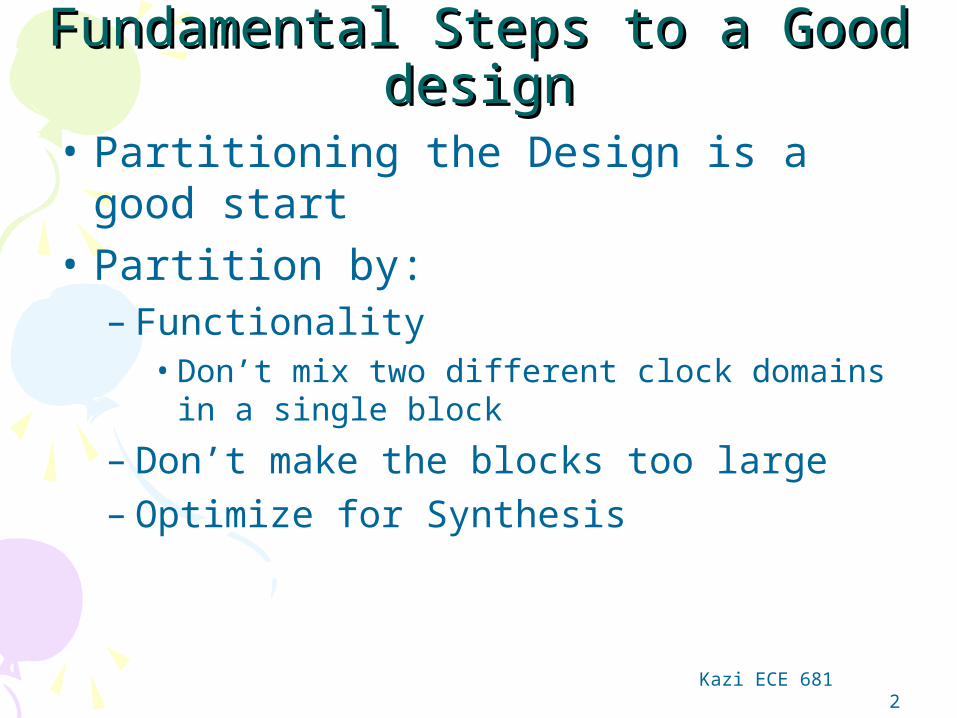
Fundamental Steps to a Good Fundamental Steps to a Good designdesign
• Partitioning the Design is a good start• Partition by:
– Functionality• Don’t mix two different clock domains in a
single block
– Don’t make the blocks too large– Optimize for Synthesis

Kazi ECE 681 3
Recommended rules for Recommended rules for SynthesisSynthesis
• When implementing combinatorial paths do not have hierarchy
• Register all outputs• Do not implement glue logic between
block, partition them well• Separate designs on functional boundary• Keep block sizes to a reasonable size• Separate core logic, pads, clock and JTAG
Kazi ECE 681 4
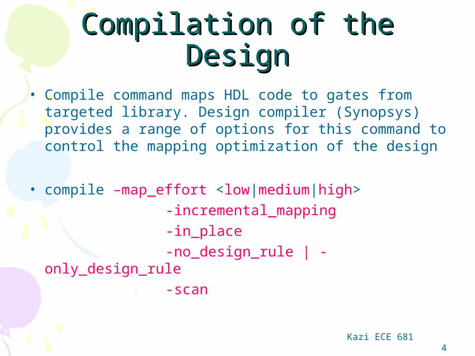
Compilation of the DesignCompilation of the Design• Compile command maps HDL code to gates from
targeted library. Design compiler (Synopsys) provides a range of options for this command to control the mapping optimization of the design
• compile –map_effort <low|medium|high> -incremental_mapping -in_place -no_design_rule | -only_design_rule -scan
Kazi ECE 681 5
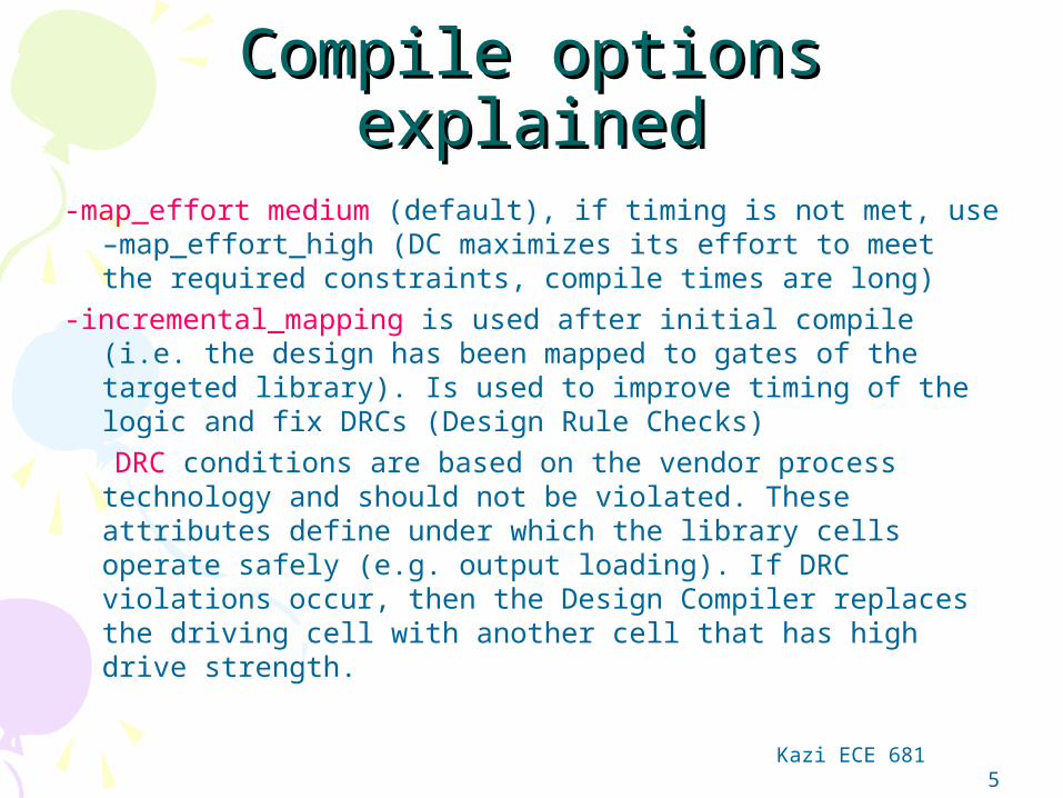
Compile options explainedCompile options explained-map_effort medium (default), if timing is not met, use –
map_effort_high (DC maximizes its effort to meet the required constraints, compile times are long)
-incremental_mapping is used after initial compile (i.e. the design has been mapped to gates of the targeted library). Is used to improve timing of the logic and fix DRCs (Design Rule Checks)
DRC conditions are based on the vendor process technology and should not be violated. These attributes define under which the library cells operate safely (e.g. output loading). If DRC violations occur, then the Design Compiler replaces the driving cell with another cell that has high drive strength.
Kazi ECE 681 6
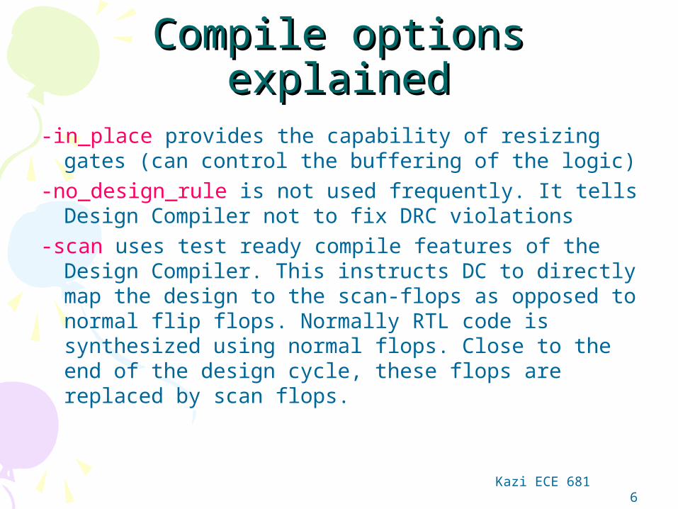
Compile options explainedCompile options explained-in_place provides the capability of resizing gates
(can control the buffering of the logic)-no_design_rule is not used frequently. It tells
Design Compiler not to fix DRC violations-scan uses test ready compile features of the
Design Compiler. This instructs DC to directly map the design to the scan-flops as opposed to normal flip flops. Normally RTL code is synthesized using normal flops. Close to the end of the design cycle, these flops are replaced by scan flops.
Kazi ECE 681 7
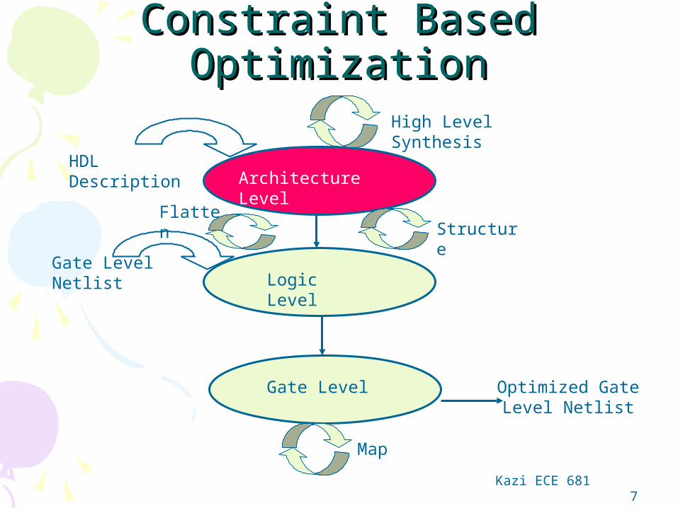
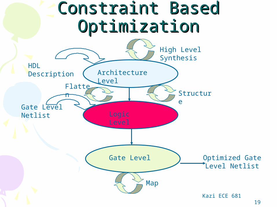
Constraint Based Constraint Based OptimizationOptimization
Architecture Level
Logic Level
Gate Level
HDL Description
High Level Synthesis
FlattenStructure
Gate Level Netlist
Map
Optimized Gate Level Netlist
Kazi ECE 681 8
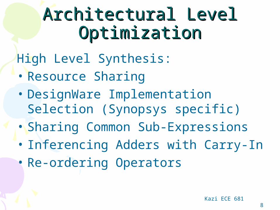
Architectural Level Architectural Level OptimizationOptimization
High Level Synthesis:• Resource Sharing• DesignWare Implementation
Selection (Synopsys specific)• Sharing Common Sub-Expressions• Inferencing Adders with Carry-In• Re-ordering Operators

Kazi ECE 681 9
Resource SharingResource SharingHDL Description if (select) then
sum <= A + B;
Else
sum <= C + D;
Mux
+
+
AB
CD
sum
select
+
muxAC
BD
sumselect
mux
One Possible Implementation
Another Implementation: shared resource Implementation -> Area-efficient
Kazi ECE 681 10
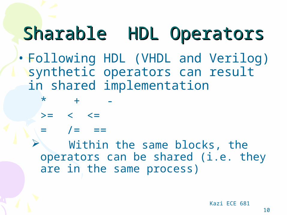
Sharable HDL OperatorsSharable HDL Operators• Following HDL (VHDL and Verilog)
synthetic operators can result in shared implementation
* + ->= < <== /= ==
Within the same blocks, the operators can be shared (i.e. they are in the same process)
Kazi ECE 681 11
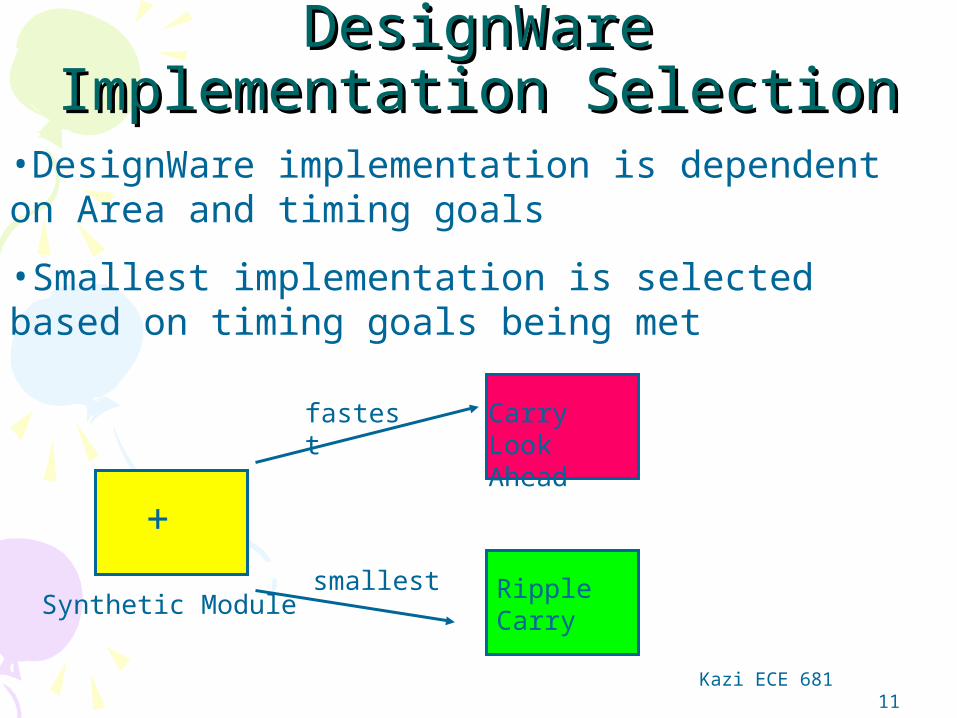
DesignWare Implementation DesignWare Implementation SelectionSelection
•DesignWare implementation is dependent on Area and timing goals
•Smallest implementation is selected based on timing goals being met
+
Synthetic Modulesmallest
fastest Carry Look Ahead
Ripple Carry
Kazi ECE 681 12
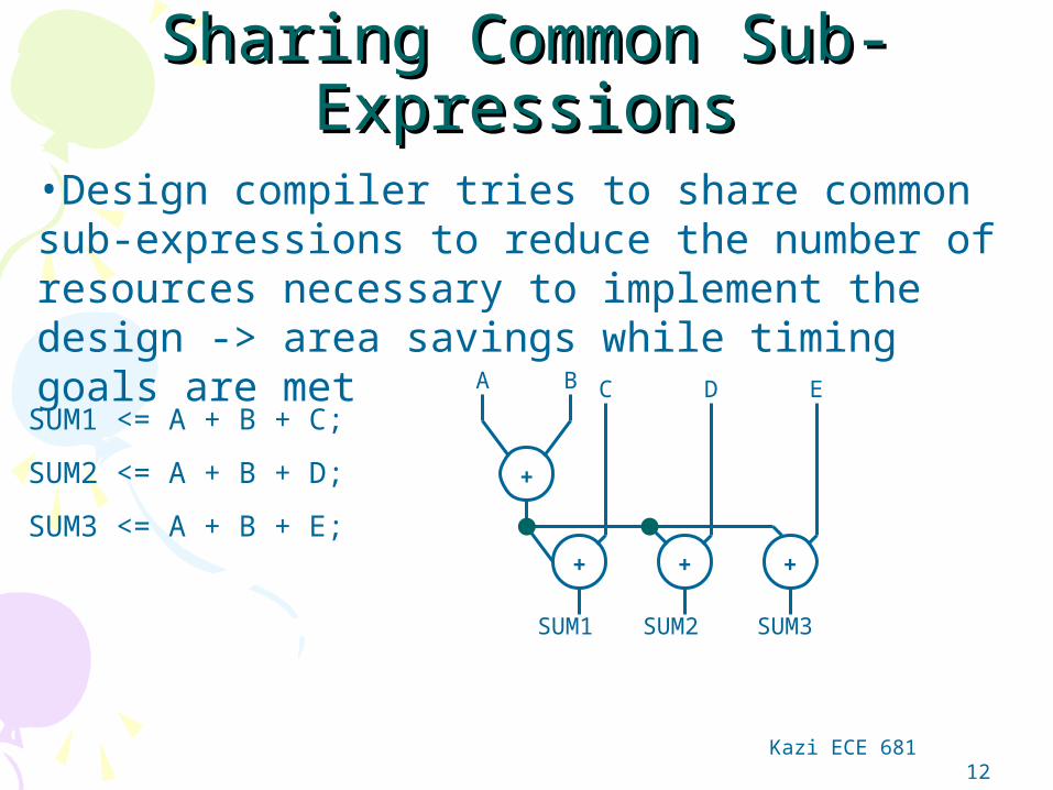
Sharing Common Sub-Sharing Common Sub-ExpressionsExpressions
•Design compiler tries to share common sub-expressions to reduce the number of resources necessary to implement the design -> area savings while timing goals are met
SUM1 <= A + B + C;
SUM2 <= A + B + D;
SUM3 <= A + B + E;+ + +
+
SUM1 SUM2 SUM3
A B C D E
Kazi ECE 681 13
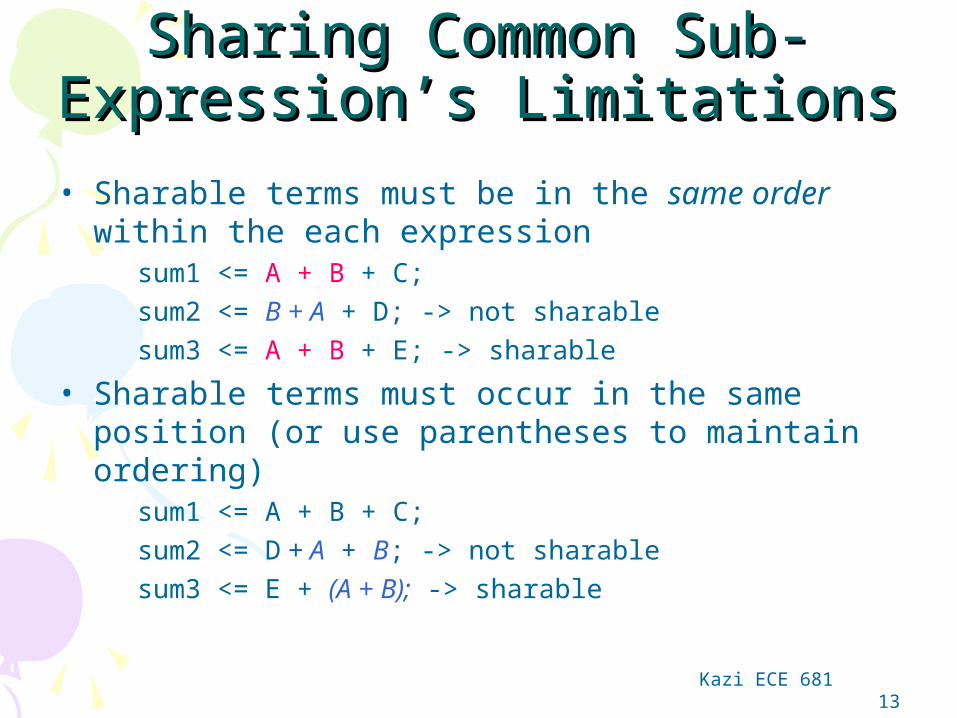
Sharing Common Sub-Sharing Common Sub-Expression’s LimitationsExpression’s Limitations
• Sharable terms must be in the same order within the each expression sum1 <= A + B + C; sum2 <= B + A + D; -> not sharable sum3 <= A + B + E; -> sharable
• Sharable terms must occur in the same position (or use parentheses to maintain ordering) sum1 <= A + B + C; sum2 <= D + A + B; -> not sharable sum3 <= E + (A + B); -> sharable
Kazi ECE 681 14
How to Infer Specific Implementation How to Infer Specific Implementation (Adder with Carry-In(Adder with Carry-In
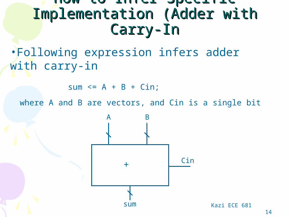
•Following expression infers adder with carry-in
sum <= A + B + Cin;
where A and B are vectors, and Cin is a single bit
A B
Cin
sum
+

Kazi ECE 681 15
Operator ReorderingOperator Reordering•Design Compiler has the capability to produce the reordering the arithmetic operators to produce the fastest design
•For example
Z <= A + B + C + D; (Z is time constrained)
Initially the ordering is from left to right
A
B
C
DZ
+
+
+

Kazi ECE 681 16
Reordering of the Operator for a Fast Reordering of the Operator for a Fast DesignDesign
•If the arrival time of all the signals, A, B, C and D is the same, the Design Compiler will reorder the operators using a balanced tree type architecture
A
B
Z
+
+
+C
D
Kazi ECE 681 17
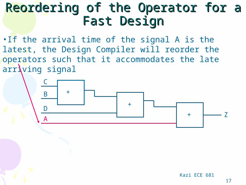
Reordering of the Operator for a Fast Reordering of the Operator for a Fast DesignDesign
•If the arrival time of the signal A is the latest, the Design Compiler will reorder the operators such that it accommodates the late arriving signal
C
B
D
AZ
+
+
+
Kazi ECE 681 18
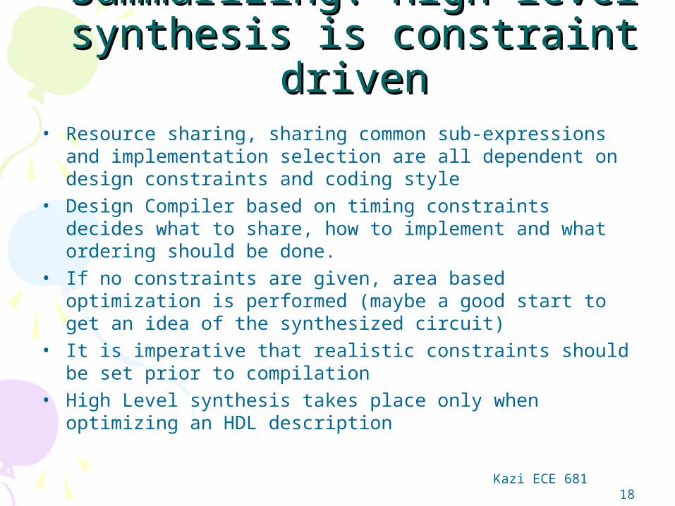
Summarizing: High level Summarizing: High level synthesis is constraint drivensynthesis is constraint driven
• Resource sharing, sharing common sub-expressions and implementation selection are all dependent on design constraints and coding style
• Design Compiler based on timing constraints decides what to share, how to implement and what ordering should be done.
• If no constraints are given, area based optimization is performed (maybe a good start to get an idea of the synthesized circuit)
• It is imperative that realistic constraints should be set prior to compilation
• High Level synthesis takes place only when optimizing an HDL description
Kazi ECE 681 19
Constraint Based Constraint Based OptimizationOptimization
Architecture Level
Logic Level
Gate Level
HDL Description
High Level Synthesis
FlattenStructure
Gate Level Netlist
Map
Optimized Gate Level Netlist
Kazi ECE 681 20
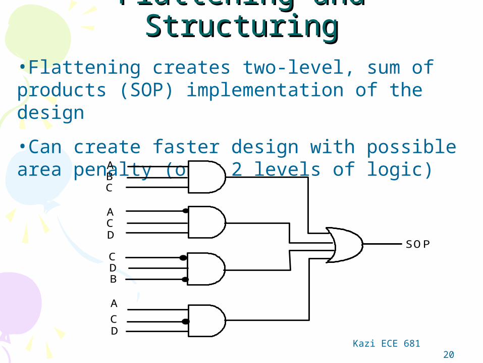
Flattening and StructuringFlattening and Structuring•Flattening creates two-level, sum of products (SOP) implementation of the design
•Can create faster design with possible area penalty (only 2 levels of logic)
ABC
ACD
CDB
A
CD
SOP
Kazi ECE 681 21
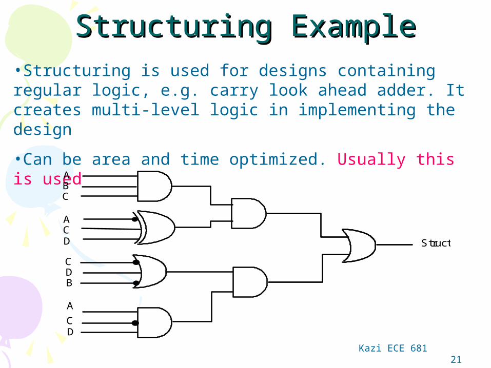
Structuring ExampleStructuring Example•Structuring is used for designs containing regular logic, e.g. carry look ahead adder. It creates multi-level logic in implementing the design
•Can be area and time optimized. Usually this is used
ABC
ACD
CDB
A
CD
Struct

Kazi ECE 681 22
Structuring ExampleStructuring Example
Before Structuring
P = ax + ay + cQ = x + y + z
After Structuring
P = aI + cQ = I + zI = x + y
Kazi ECE 681 23
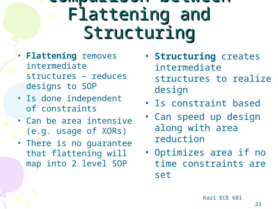
Comparison between Comparison between Flattening and StructuringFlattening and Structuring
• Flattening removes intermediate structures – reduces designs to SOP
• Is done independent of constraints
• Can be area intensive (e.g. usage of XORs)
• There is no guarantee that flattening will map into 2 level SOP
• Structuring creates intermediate structures to realize design
• Is constraint based• Can speed up design
along with area reduction• Optimizes area if no time
constraints are set
Kazi ECE 681 24
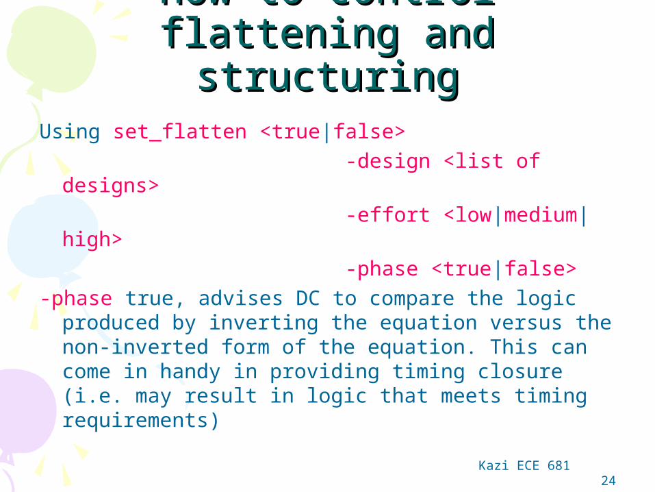
How to control flattening How to control flattening and structuringand structuring
Using set_flatten <true|false> -design <list of designs> -effort <low|medium|high> -phase <true|false>-phase true, advises DC to compare the logic
produced by inverting the equation versus the non-inverted form of the equation. This can come in handy in providing timing closure (i.e. may result in logic that meets timing requirements)
Kazi ECE 681 25
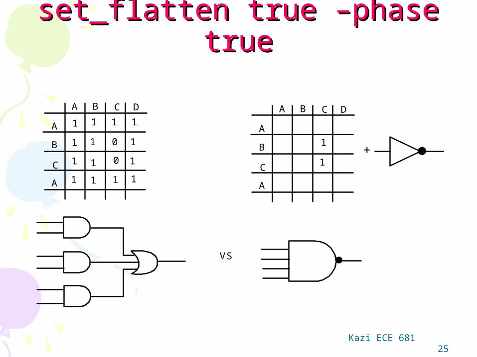
set_flatten true –phase trueset_flatten true –phase true
A
B
C
A
1
BA C D
111
1111
1
1
1
1
1
10
0
A
B
C
A
BA C D
1
1+
VS

Kazi ECE 681 26
Example of SONET Framing Example of SONET Framing block in a framer ASICblock in a framer ASIC
A1 A2
1 2 3 4 5 ………….. ………. 90th byte
1
2
3
4
5
6
7
8
9
A1 = hexF6, A2 = hex28; is the framing pattern used in SONET networks; Order or transmission is F6 (11110110) msb transmitted first. All bytes other than A1 and A2 are scrambled
Kazi ECE 681 27
Data Com bytes (D1-D3)Data Com bytes (D1-D3)• D1-D3 bytes are the 1st three bytes in
the 3rd row of the STS-1 frame. These bytes are used as a 192 kbps data channel for operations functions, such as Operations, Administration, Management and Provisioning (OAM&P). These bytes are used between 2 “section” type equipment (like regenerator)
Kazi ECE 681 28
Data Com bytes D4-D12Data Com bytes D4-D12• These bytes (1st three bytes of rows
6,7 and 8) represent a 576 kbps message-based channel used for OAM&P messages between SONET line-level network equipment.
Kazi ECE 681 29
Assignment 1 continuedAssignment 1 continued• Use the SONET scramble to scramble the data (except A1
and A1 bytes)• Calculate B1and insert it in the next SONET frame• Use PRBS pattern generator to insert in the 3 Data Com
bytes D1-D3 byte positions
• Take first 9 characters of your name and convert them into ASCII (bit value). Insert those values in the D4-D12 byte positions.
• The D1-D3 and D4-D12 data should come out on separate serial ports along with 192 kbps and 576 kbps clock. The firs byte should be indicated by a start of frame signal. (3 ports per Data com bytes should be output ports from your block, therefore total of 6 output ports)
Kazi ECE 681 30
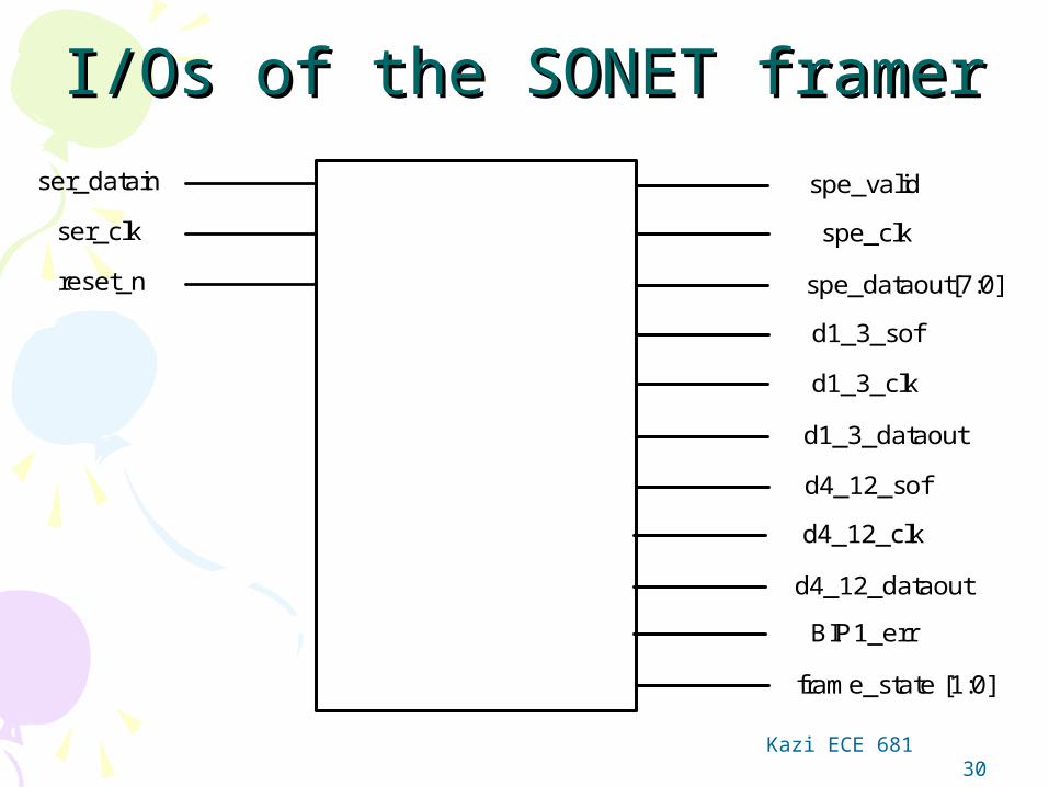
I/Os of the SONET framerI/Os of the SONET framer
ser_datain
ser_clk
reset_n
spe_valid
spe_clk
spe_dataout[7:0]
d1_3_sof
d1_3_clk
d1_3_dataout
d4_12_sof
d4_12_clk
d4_12_dataout
BIP1_err
frame_state [1:0]


![vlsi & embedded systems lab - SIETK ECE DEPARTMENT · 2018. 7. 16. · SIETK, ECE [VLSI & EMBEDDED SYSTEMS LAB] 2 (15A04712) VLSI & EMBEDDED SYSTEMS LABORATORY Note: The students](https://img.pdfslide.us/doc/110x75/60a68df82b16b22c09239fcb/vlsi-embedded-systems-lab-sietk-ece-department-2018-7-16-sietk-ece.jpg)


![Ece-V-fundamentals of Cmos Vlsi [10ec56]-Solution](https://img.pdfslide.us/doc/110x75/55cf9d28550346d033ac77f4/ece-v-fundamentals-of-cmos-vlsi-10ec56-solution.jpg)