Embed Size (px)
Citation preview


ECE 477 Design Review ECE 477 Design Review Team 3 Team 3 Fall 2007 Fall 2007
StevenKingsley(Analog)
RoyScheck(Leader)
TonyLiechty(Digital)
CharlesLan
(Software)

OutlineOutline• Project overview Project overview • Project-specific success criteriaProject-specific success criteria• Block diagramBlock diagram• Component selection rationaleComponent selection rationale• Packaging designPackaging design• Schematic and theory of operationSchematic and theory of operation• PCB layoutPCB layout• Software design/development statusSoftware design/development status• Project completion timelineProject completion timeline• Questions / discussionQuestions / discussion

Project OverviewProject Overview
• Allows a single note instrument to be used Allows a single note instrument to be used as a MIDI instrumentas a MIDI instrument
• Ability to tune the instrument for more Ability to tune the instrument for more accurate MIDI conversionaccurate MIDI conversion
• MIDI is an audio standardMIDI is an audio standard• Software allows real time composition of Software allows real time composition of
music from MIDImusic from MIDI
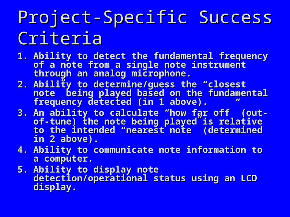
Project-Specific Success CriteriaProject-Specific Success Criteria
1.1. Ability to detect the fundamental frequency of a Ability to detect the fundamental frequency of a note from a single note instrument through an note from a single note instrument through an analog microphone.analog microphone.
2.2. Ability to determine/guess the “closest note” being Ability to determine/guess the “closest note” being played based on the fundamental frequency played based on the fundamental frequency detected (in 1 above).detected (in 1 above).
3.3. An ability to calculate “how far off” (out-of-tune) An ability to calculate “how far off” (out-of-tune) the note being played is relative to the intended the note being played is relative to the intended “nearest note” (determined in 2 above).“nearest note” (determined in 2 above).
4.4. Ability to communicate note information to a Ability to communicate note information to a computer.computer.
5.5. Ability to display note detection/operational status Ability to display note detection/operational status using an LCD display.using an LCD display.

Block DiagramBlock Diagram
PreAmp FilterMicrophone
DSP
LCD
USB interface
ATD
Volume Control
Parallel
GPIO
2
SPI
7
I2C
4
Volume Knob
2PWM
GPIO
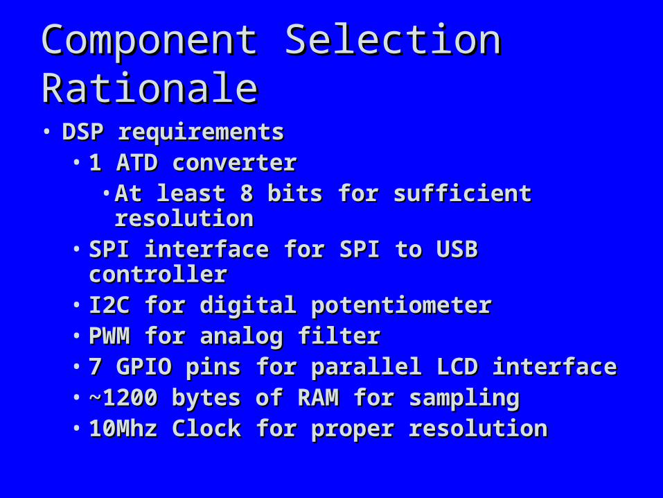
Component Selection RationaleComponent Selection Rationale
• DSP requirementsDSP requirements• 1 ATD converter1 ATD converter
• At least 8 bits for sufficient resolutionAt least 8 bits for sufficient resolution• SPI interface for SPI to USB controllerSPI interface for SPI to USB controller• I2C for digital potentiometerI2C for digital potentiometer• PWM for analog filterPWM for analog filter• 7 GPIO pins for parallel LCD interface7 GPIO pins for parallel LCD interface• ~1200 bytes of RAM for sampling~1200 bytes of RAM for sampling• 10Mhz Clock for proper resolution10Mhz Clock for proper resolution

Component Selection RationaleComponent Selection Rationale
• Possible DSPsPossible DSPs– Freescale 56F8014Freescale 56F8014
• 16 Kbyte flash, 4 Kbyte RAM16 Kbyte flash, 4 Kbyte RAM• 32 Mhz Clock, 32 pins32 Mhz Clock, 32 pins• $3.15 in 1,000 quantities $3.15 in 1,000 quantities
– Atmel AT32UC3B164 Atmel AT32UC3B164 • 64 Kbyte flash, 16 Kbyte RAM64 Kbyte flash, 16 Kbyte RAM• 90 Mhz Clock, 48 pins90 Mhz Clock, 48 pins• $4.66 in 10,000 quantities $4.66 in 10,000 quantities • NewerNewer
Component Selection RationaleComponent Selection Rationale
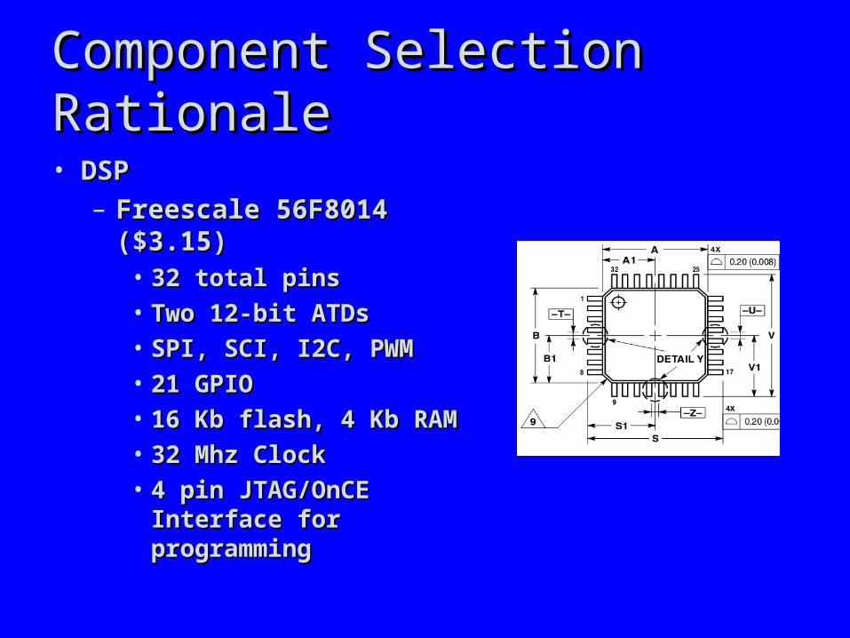
• DSPDSP– Freescale 56F8014 ($3.15)Freescale 56F8014 ($3.15)
• 32 total pins32 total pins
• Two 12-bit ATDsTwo 12-bit ATDs
• SPI, SCI, I2C, PWMSPI, SCI, I2C, PWM
• 21 GPIO21 GPIO
• 16 Kb flash, 4 Kb RAM16 Kb flash, 4 Kb RAM
• 32 Mhz Clock32 Mhz Clock
• 4 pin JTAG/OnCE Interface 4 pin JTAG/OnCE Interface for programmingfor programming
Component Selection RationaleComponent Selection Rationale
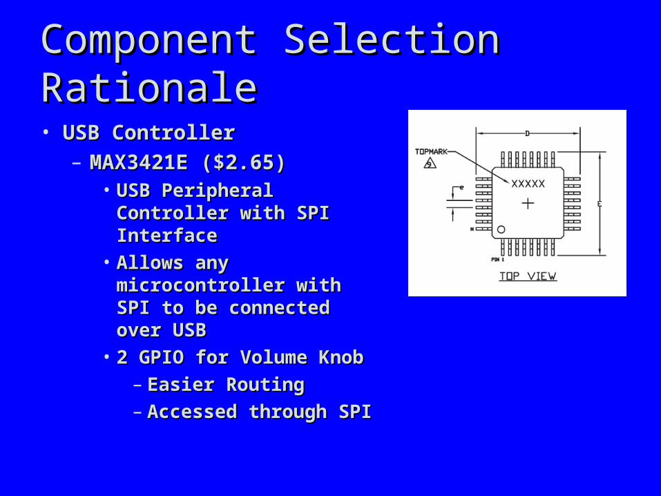
• USB ControllerUSB Controller– MAX3421E ($2.65)MAX3421E ($2.65)
• USB Peripheral Controller USB Peripheral Controller with SPI Interfacewith SPI Interface
• Allows any Allows any microcontroller with SPI microcontroller with SPI to be connected over USBto be connected over USB
• 2 GPIO for Volume Knob 2 GPIO for Volume Knob
– Easier RoutingEasier Routing
– Accessed through SPIAccessed through SPI

Component Selection RationaleComponent Selection Rationale
• LCDLCD– CFAH1602B-YTI-JP CFAH1602B-YTI-JP
• 4 bit parallel interface (4 pins)4 bit parallel interface (4 pins)• 3 bit functionality (3 pins)3 bit functionality (3 pins)• Power consumptionPower consumption
– 1.5 ma for LCD1.5 ma for LCD– 150 ma for Backlight150 ma for Backlight

Packaging DesignPackaging Design
• Form FactorForm Factor– Small for mobilitySmall for mobility– Sloped panel for easy viewing and better Sloped panel for easy viewing and better
microphone receptionmicrophone reception
• Packaging FeaturesPackaging Features– LCD display of Note Information and VolumeLCD display of Note Information and Volume– Incoming Signal Amplifier (Rotary Knob)Incoming Signal Amplifier (Rotary Knob)– Internal MicrophoneInternal Microphone– USB Interface (Female “B” Adapter)USB Interface (Female “B” Adapter)

Packaging DesignPackaging Design
• Hammond 1456CE2Hammond 1456CE2
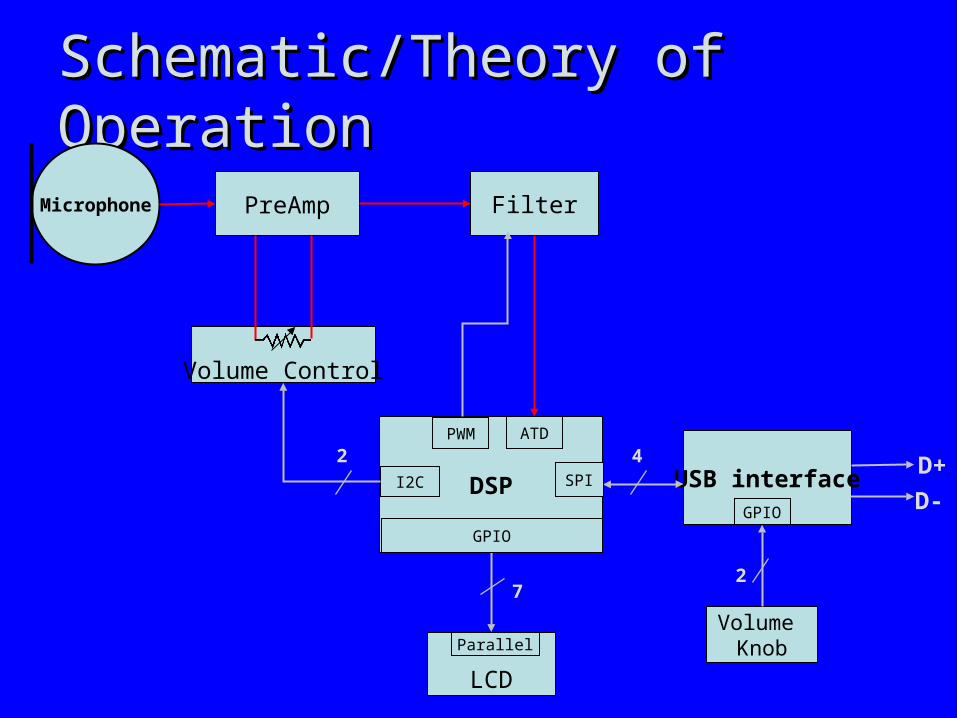
Schematic/Theory of OperationSchematic/Theory of Operation
PreAmp FilterMicrophone
DSP
LCD
USB interface
ATD
Volume Control
D+
D-
Parallel
GPIO
2
SPI
7
I2C
4
Volume Knob
2PWM
GPIO

Schematic/Theory of OperationSchematic/Theory of Operation• Power Supplies (3.3V, 1 Amp)Power Supplies (3.3V, 1 Amp)
– Separate Analog and Digital suppliesSeparate Analog and Digital supplies

Schematic/Theory of OperationSchematic/Theory of Operation
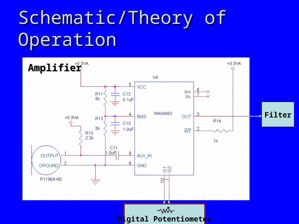
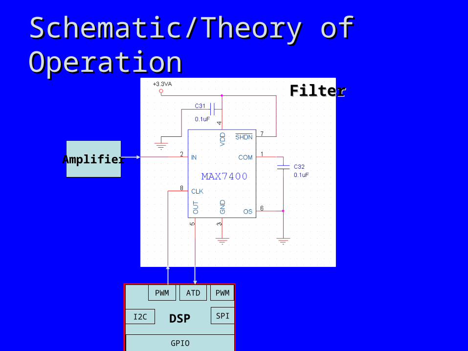
• AnalogAnalog– Amplify and Bias at 1.65VAmplify and Bias at 1.65V– FilterFilter
10 mV
-10 mV
0 V
3 V
0 V
Schematic/Theory of OperationSchematic/Theory of Operation
Filter
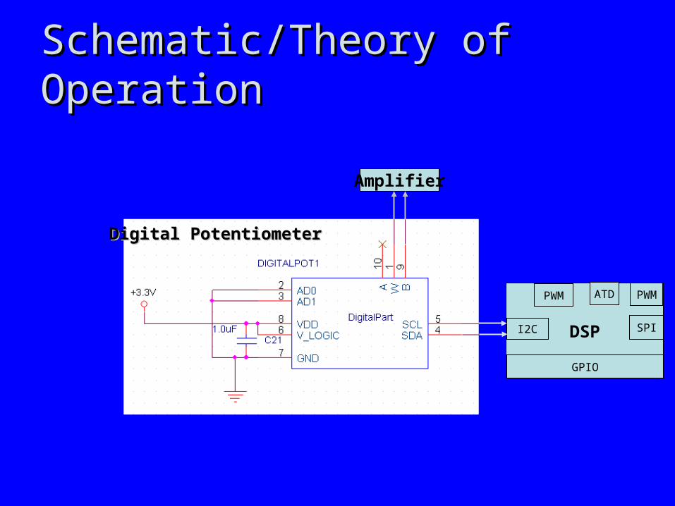
Digital Potentiometer
AmplifierAmplifier
Schematic/Theory of OperationSchematic/Theory of Operation
Digital PotentiometerDigital Potentiometer
Amplifier
DSP
ATD
GPIO
SPII2C
PWM PWM
Schematic/Theory of OperationSchematic/Theory of Operation
Amplifier
DSP
ATD
GPIO
SPII2C
PWM
FilterFilter
PWM

Schematic/Theory of OperationSchematic/Theory of Operation
USB interface
D+ D-
LCD
Parallel
OnCE
Volume ControlFilter
Clock
Interrupt
DSP

Schematic/Theory of OperationSchematic/Theory of Operation
DSP
ATD
GPIO
SPII2C
PWM PWM
SPI To USB

Schematic/Theory of OperationSchematic/Theory of Operation
DSP
ATD
GPIO
SPII2C
PWM PWM
GroundHeader

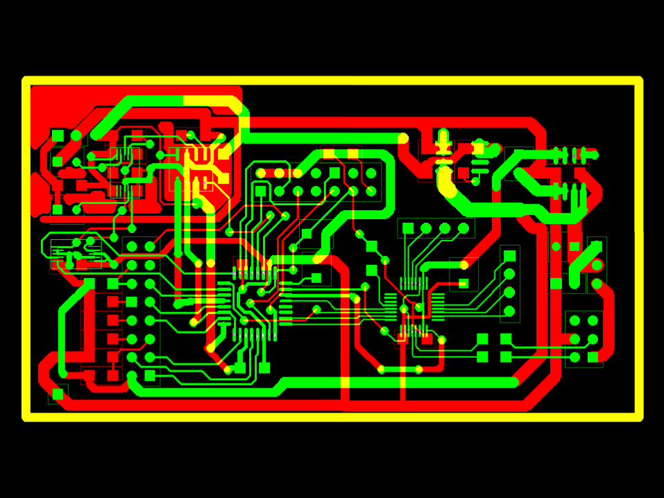
PCB LayoutPCB Layout
• General Design General Design ConsiderationsConsiderations
• Specific Design Specific Design ConsiderationsConsiderations– Power SupplyPower Supply– AnalogAnalog– DigitalDigital

PCB LayoutPCB Layout
• General Design General Design ConsiderationsConsiderations– Overall low power Overall low power
consumptionconsumption• General trace General trace
width of 10 milswidth of 10 mils– Separate Analog and Separate Analog and
Digital systemsDigital systems– Minimize trace lengthMinimize trace length– Minimize anglesMinimize angles

PCB LayoutPCB Layout
• Power Supply Design Power Supply Design ConsiderationsConsiderations– Separate Analog and Separate Analog and
DigitalDigital• Separate GroundsSeparate Grounds
– 5 V Unregulated Supply5 V Unregulated Supply• Trace width of 80 milsTrace width of 80 mils
– 3.3 V Regulated Supply3.3 V Regulated Supply• Trace width of 70 milsTrace width of 70 mils
– Bypass CapacitorsBypass Capacitors• Placed directly Placed directly
beneath Voltage beneath Voltage RegulatorsRegulators

PCB LayoutPCB Layout
• Analog Design Analog Design ConsiderationsConsiderations– High sensitivityHigh sensitivity
• Ground shieldingGround shielding• Copper PourCopper Pour
– MicrophoneMicrophone• Minimize leadsMinimize leads
– Bypass CapacitorsBypass Capacitors• Placed directly Placed directly
beneath beneath respective ICrespective IC

PCB LayoutPCB Layout
• Digital Design Digital Design ConsiderationsConsiderations– Bypass CapacitorsBypass Capacitors
• Placed directly Placed directly beneath beneath MicrocontrollerMicrocontroller
– Bulk CapacitorsBulk Capacitors• Placed further from Placed further from
MicrocontrollerMicrocontroller– General Purpose I/O PinsGeneral Purpose I/O Pins
• Assigned to Assigned to corresponding side to corresponding side to minimize lengthminimize length


Software Design/Development StatusSoftware Design/Development Status
• Three options for developmentThree options for development– JTAG/OnCEJTAG/OnCE
• Easy to debugEasy to debug• Costly Development boardCostly Development board
– SCI serial bootloaderSCI serial bootloader• Frees up more pinsFrees up more pins• Addition of level translators and RS232 Addition of level translators and RS232
implementationimplementation– Bulk device programmerBulk device programmer
• Hard to debug after packagingHard to debug after packaging• Easy to program multiple chipsEasy to program multiple chips
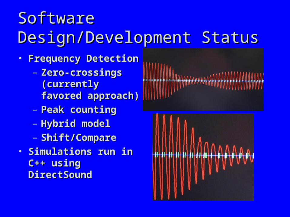
Software Design/Development Software Design/Development StatusStatus• Frequency DetectionFrequency Detection
– Zero-crossings Zero-crossings (currently favored (currently favored approach)approach)
– Peak countingPeak counting– Hybrid modelHybrid model– Shift/CompareShift/Compare
• Simulations run in C++ Simulations run in C++ using DirectSoundusing DirectSound

Project Completion TimelineProject Completion TimelineWeek # 1 2 3 4 5 6 7 8 9 10 11 12 13 14 15 16
PCB
Assembly of PCB
Software
Packaging
Testing
Documentation
Research
Schematic
Project Finalization
Thanksgiving
Current Week

Questions / DiscussionQuestions / Discussion