Embed Size (px)
Citation preview
ECE 448: Lab 5
Serial Communications
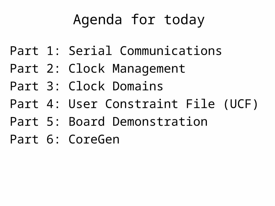
Part 1: Serial Communications
Part 2: Clock Management
Part 3: Clock Domains
Part 4: User Constraint File (UCF)
Part 5: Board Demonstration
Part 6: CoreGen
Agenda for today

Part 1
Serial Communications
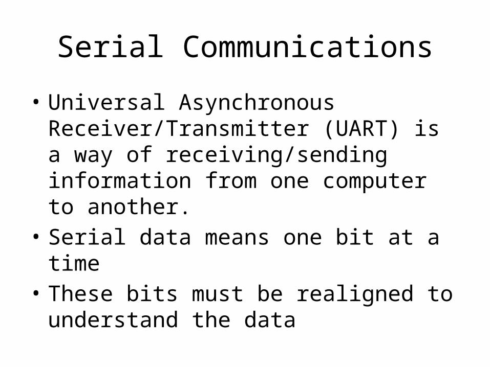
Serial Communications
• Universal Asynchronous Receiver/Transmitter (UART) is a way of receiving/sending information from one computer to another.
• Serial data means one bit at a time • These bits must be realigned to understand
the data
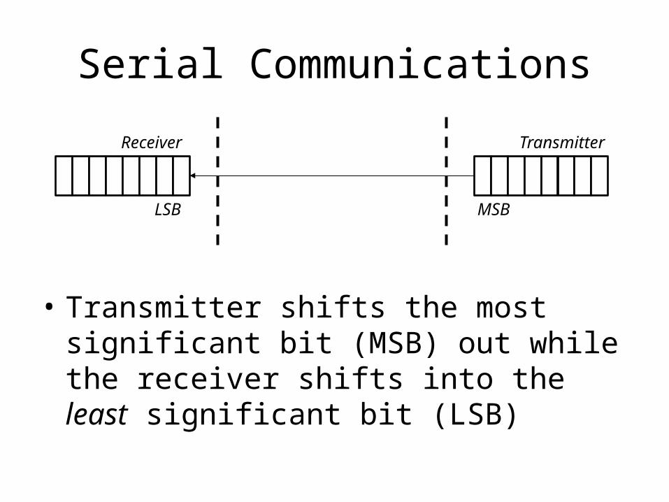
Serial Communications
• Transmitter shifts the most significant bit (MSB) out while the receiver shifts into the least significant bit (LSB)
Receiver Transmitter
LSB MSB
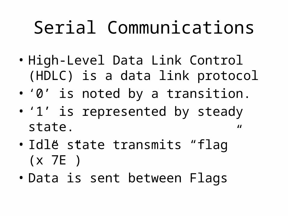
Serial Communications
• High-Level Data Link Control (HDLC) is a data link protocol
• ‘0’ is noted by a transition.• ‘1’ is represented by steady state.• Idle state transmits “flag” (x”7E”)• Data is sent between Flags
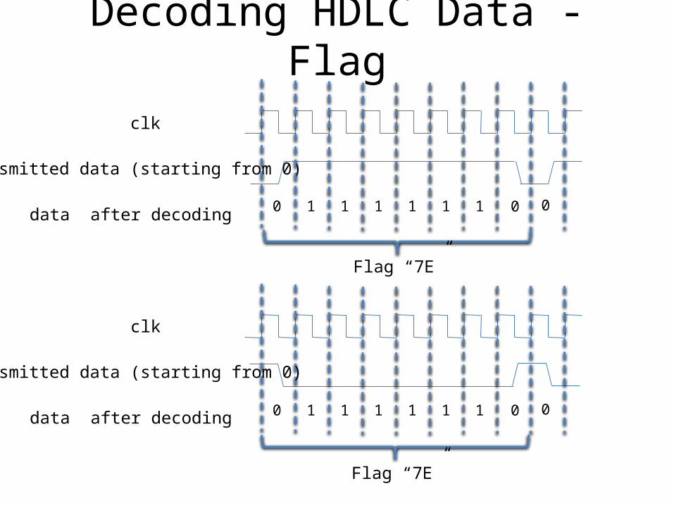
Decoding HDLC Data - Flag
10 1 1 1 1 1 0
clk
transmitted data (starting from 0)
data after decoding0
10 1 1 1 1 1 0 0
clk
transmitted data (starting from 0)
data after decoding
Flag “7E”
Flag “7E”
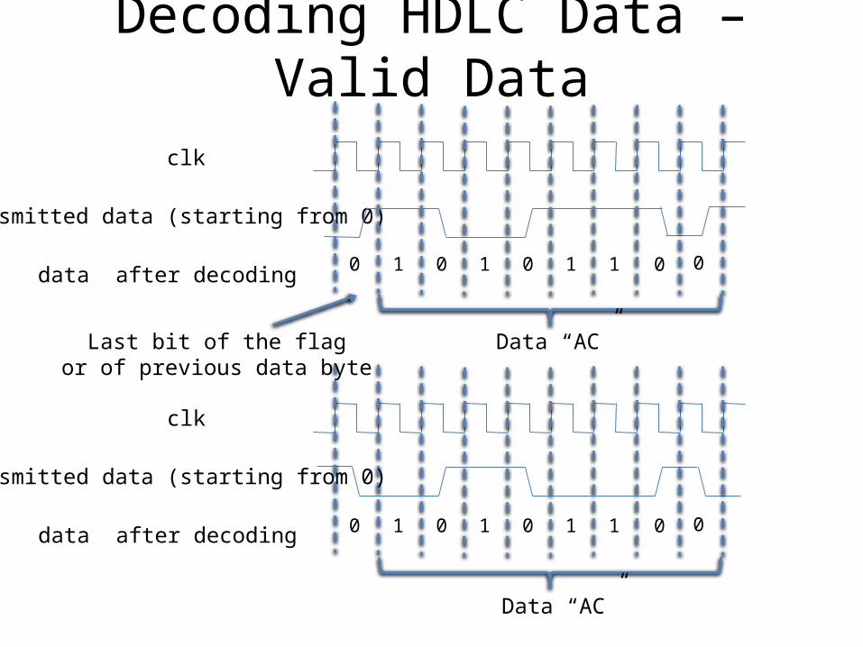
Decoding HDLC Data – Valid Data
10 0 1 0 1 1 0
clk
transmitted data (starting from 0)
data after decoding0
10 0 1 0 1 1 0 0
clk
transmitted data (starting from 0)
data after decoding
Data “AC”
Data “AC”
Last bit of the flagor of previous data byte
Serial Communications
• Since x”7E” denotes flag, there needs to be protection from finding this in the data stream
• Every time five consecutive ‘1’s are found in the data, an extra ‘0’ is inserted. Receiver knows to discard this bit
• This does two things:– Helps bit alignment– Since energy is in transitions, old PLLs maintain
enough energy to stay locked
Serial Communications
• Phase alignment– Since flag is unique, we can align by recognizing
flag– When we get six ‘1’s in a row, next bit must be bit
7 of flag– Therefore bit 0 of new flag or data is coming soon
Part 2
Clock Management
Clock Management
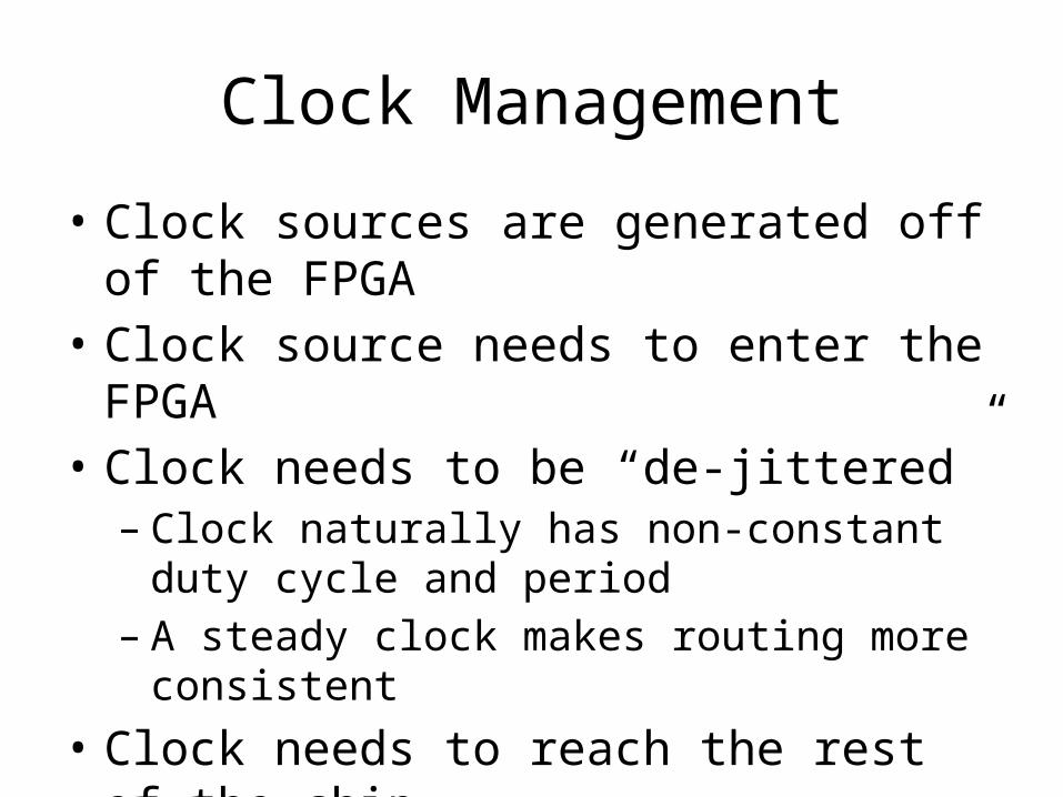
• Clock sources are generated off of the FPGA• Clock source needs to enter the FPGA• Clock needs to be “de-jittered”
– Clock naturally has non-constant duty cycle and period
– A steady clock makes routing more consistent• Clock needs to reach the rest of the chip
Clock Management
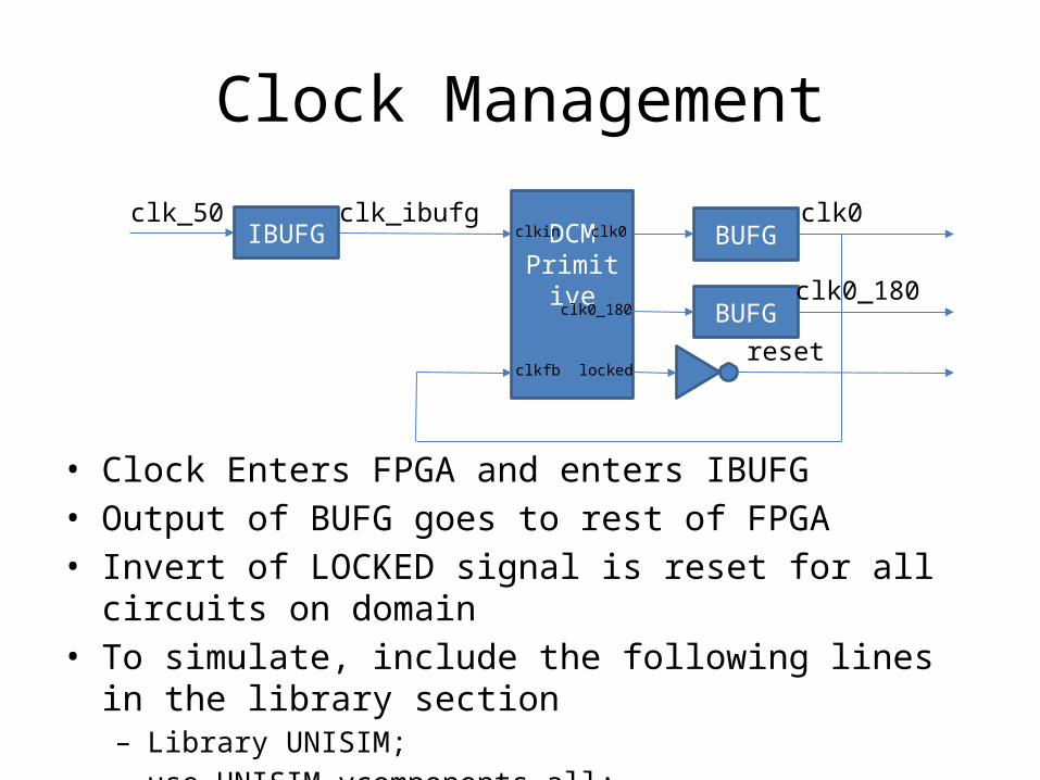
• Clock Enters FPGA and enters IBUFG• Output of BUFG goes to rest of FPGA• Invert of LOCKED signal is reset for all circuits on domain• To simulate, include the following lines in the library section
– Library UNISIM;– use UNISIM.vcomponents.all;
DCM Primitive
IBUFG BUFGclk_50
locked
clk0_180
clk_ibufg clk0
reset
clkin
clkfb
clk0
BUFGclk0_180
Clock Management
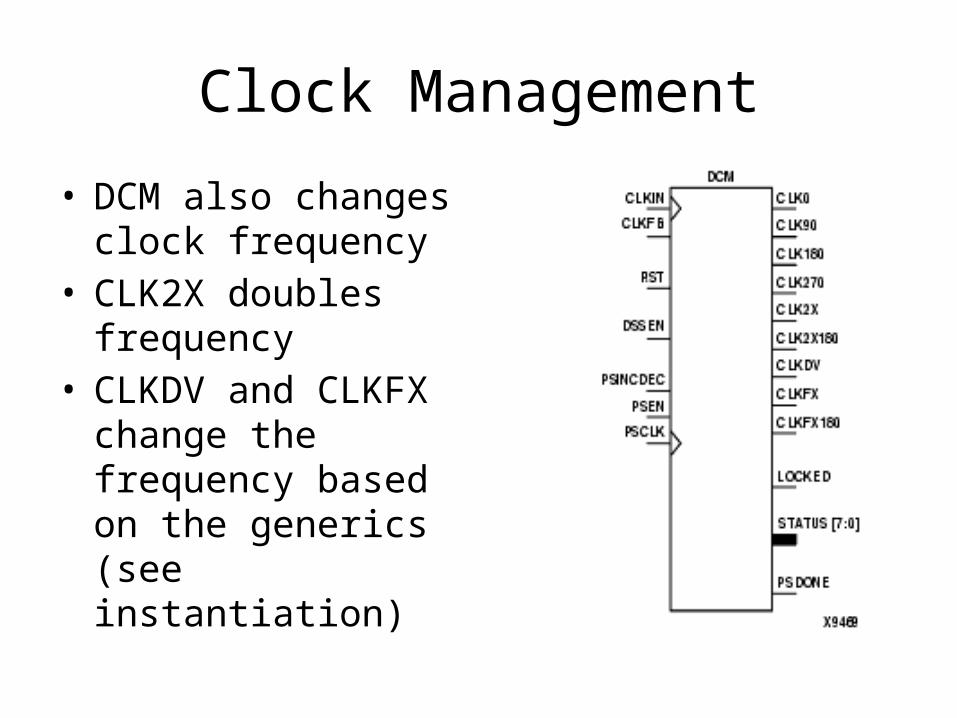
• DCM also changes clock frequency
• CLK2X doubles frequency
• CLKDV and CLKFX change the frequency based on the generics (see instantiation)
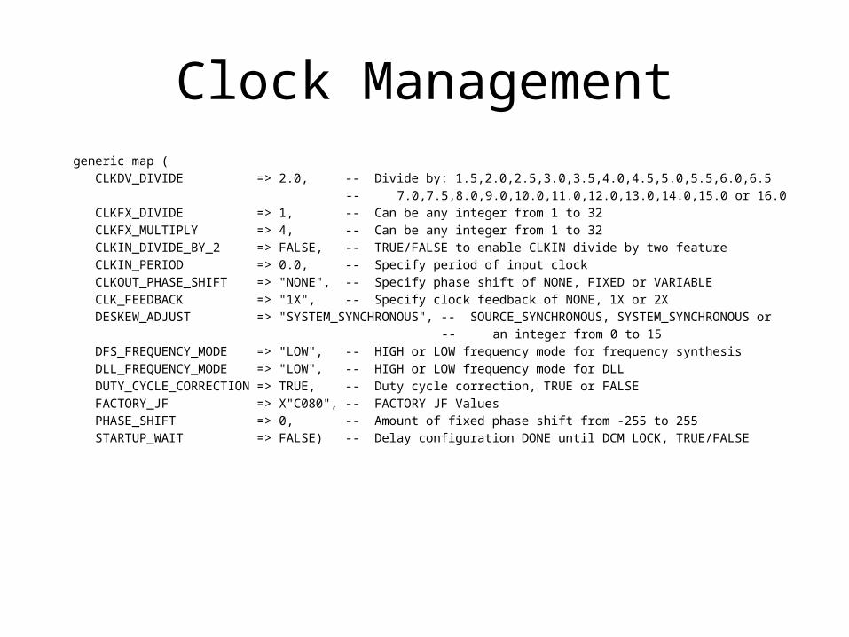
Clock Management generic map ( CLKDV_DIVIDE => 2.0, -- Divide by: 1.5,2.0,2.5,3.0,3.5,4.0,4.5,5.0,5.5,6.0,6.5 -- 7.0,7.5,8.0,9.0,10.0,11.0,12.0,13.0,14.0,15.0 or 16.0 CLKFX_DIVIDE => 1, -- Can be any integer from 1 to 32 CLKFX_MULTIPLY => 4, -- Can be any integer from 1 to 32 CLKIN_DIVIDE_BY_2 => FALSE, -- TRUE/FALSE to enable CLKIN divide by two feature CLKIN_PERIOD => 0.0, -- Specify period of input clock CLKOUT_PHASE_SHIFT => "NONE", -- Specify phase shift of NONE, FIXED or VARIABLE CLK_FEEDBACK => "1X", -- Specify clock feedback of NONE, 1X or 2X DESKEW_ADJUST => "SYSTEM_SYNCHRONOUS", -- SOURCE_SYNCHRONOUS, SYSTEM_SYNCHRONOUS or -- an integer from 0 to 15 DFS_FREQUENCY_MODE => "LOW", -- HIGH or LOW frequency mode for frequency synthesis DLL_FREQUENCY_MODE => "LOW", -- HIGH or LOW frequency mode for DLL DUTY_CYCLE_CORRECTION => TRUE, -- Duty cycle correction, TRUE or FALSE FACTORY_JF => X"C080", -- FACTORY JF Values PHASE_SHIFT => 0, -- Amount of fixed phase shift from -255 to 255 STARTUP_WAIT => FALSE) -- Delay configuration DONE until DCM LOCK, TRUE/FALSE
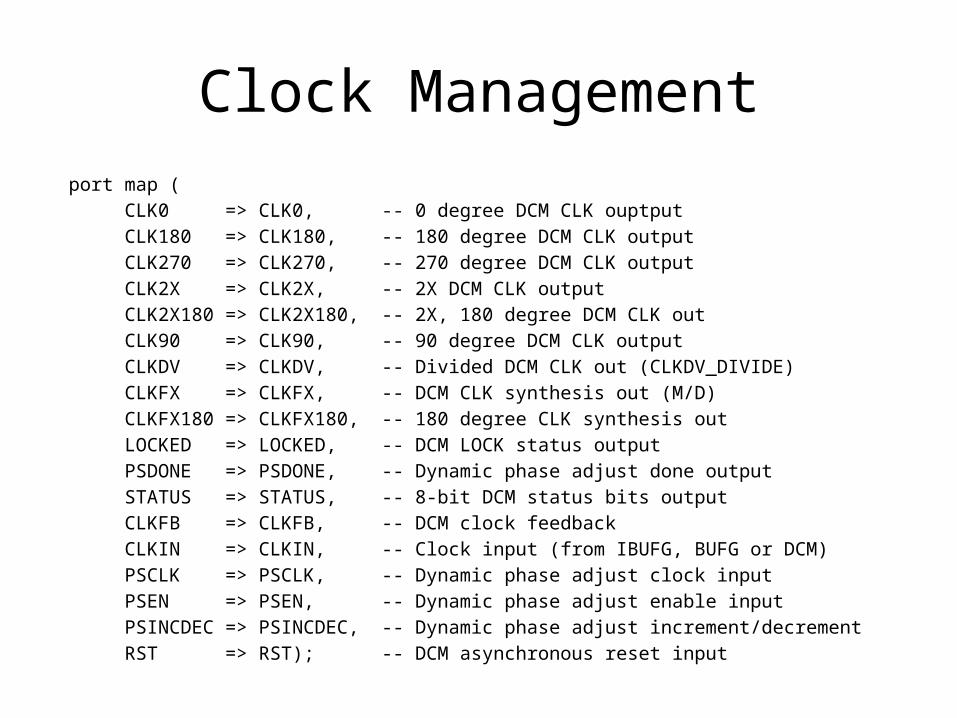
Clock Management port map ( CLK0 => CLK0, -- 0 degree DCM CLK ouptput CLK180 => CLK180, -- 180 degree DCM CLK output CLK270 => CLK270, -- 270 degree DCM CLK output CLK2X => CLK2X, -- 2X DCM CLK output CLK2X180 => CLK2X180, -- 2X, 180 degree DCM CLK out CLK90 => CLK90, -- 90 degree DCM CLK output CLKDV => CLKDV, -- Divided DCM CLK out (CLKDV_DIVIDE) CLKFX => CLKFX, -- DCM CLK synthesis out (M/D) CLKFX180 => CLKFX180, -- 180 degree CLK synthesis out LOCKED => LOCKED, -- DCM LOCK status output PSDONE => PSDONE, -- Dynamic phase adjust done output STATUS => STATUS, -- 8-bit DCM status bits output CLKFB => CLKFB, -- DCM clock feedback CLKIN => CLKIN, -- Clock input (from IBUFG, BUFG or DCM) PSCLK => PSCLK, -- Dynamic phase adjust clock input PSEN => PSEN, -- Dynamic phase adjust enable input PSINCDEC => PSINCDEC, -- Dynamic phase adjust increment/decrement RST => RST); -- DCM asynchronous reset input
Part 3
Clock Domains
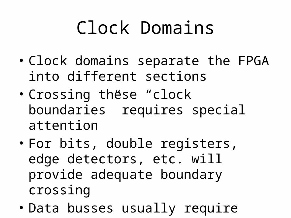
Clock Domains
• Clock domains separate the FPGA into different sections
• Crossing these “clock boundaries” requires special attention
• For bits, double registers, edge detectors, etc. will provide adequate boundary crossing
• Data busses usually require more attention i.e. FIFOs (First In/First Out)
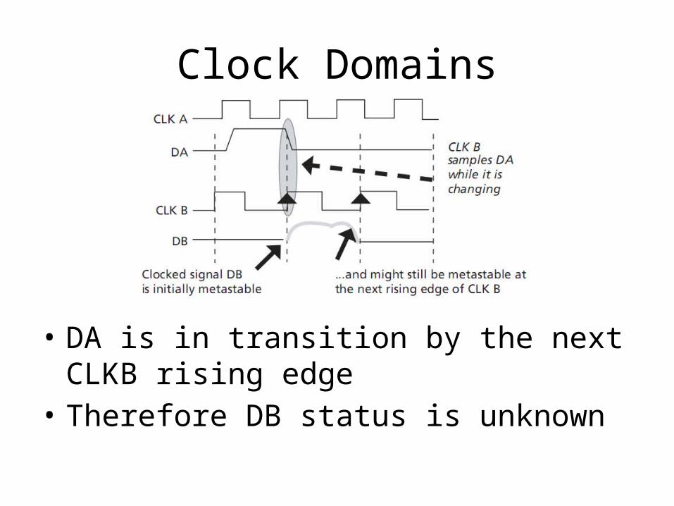
Clock Domains
• DA is in transition by the next CLKB rising edge• Therefore DB status is unknown
Clock Domains
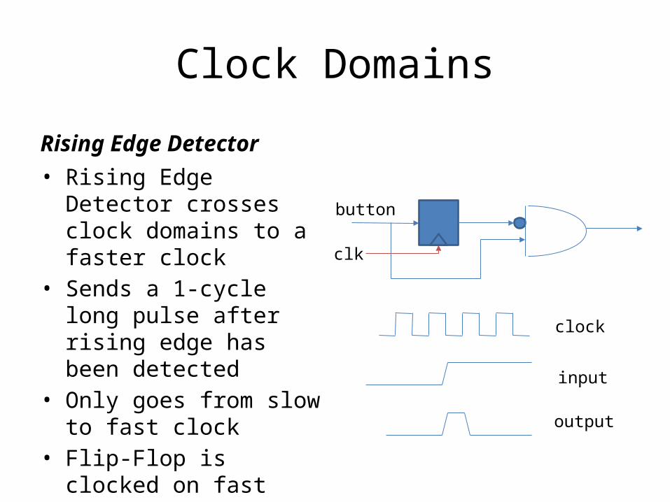
Rising Edge Detector• Rising Edge Detector
crosses clock domains to a faster clock
• Sends a 1-cycle long pulse after rising edge has been detected
• Only goes from slow to fast clock
• Flip-Flop is clocked on fast domain clock
clock
input
output
button
clk
Clock Domains
TX
RX
FP
GA
8
88
rx_clk
rxd
clk0_180
txd
FIFOwr_en rd_en
din dout
clk1krx_clk
FP
GA
Switches
Buttons
4x7seg display
SSegCtrl
debounce
btn
button(1)
button(0)
8
4
seg
an
JAJD
RED
RED
wr_clk
rd_clk
clk0
Clock Domains
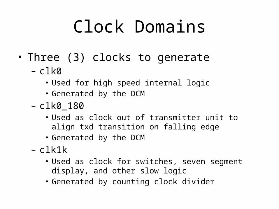
• Three (3) clocks to generate– clk0
• Used for high speed internal logic• Generated by the DCM
– clk0_180• Used as clock out of transmitter unit to align txd transition on
falling edge• Generated by the DCM
– clk1k• Used as clock for switches, seven segment display, and other slow
logic• Generated by counting clock divider
Clock Domains
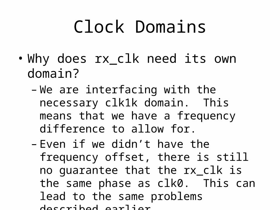
• Why does rx_clk need its own domain?– We are interfacing with the necessary clk1k
domain. This means that we have a frequency difference to allow for.
– Even if we didn’t have the frequency offset, there is still no guarantee that the rx_clk is the same phase as clk0. This can lead to the same problems described earlier.
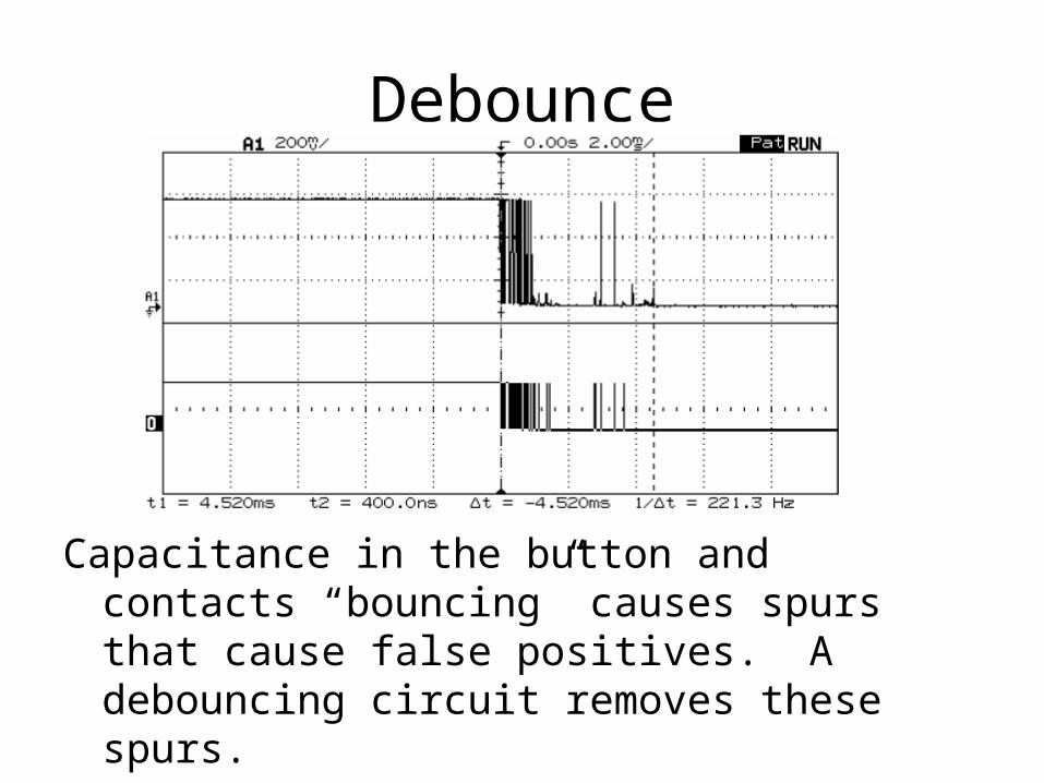
Debounce
Capacitance in the button and contacts “bouncing” causes spurs that cause false positives. A debouncing circuit removes these spurs.
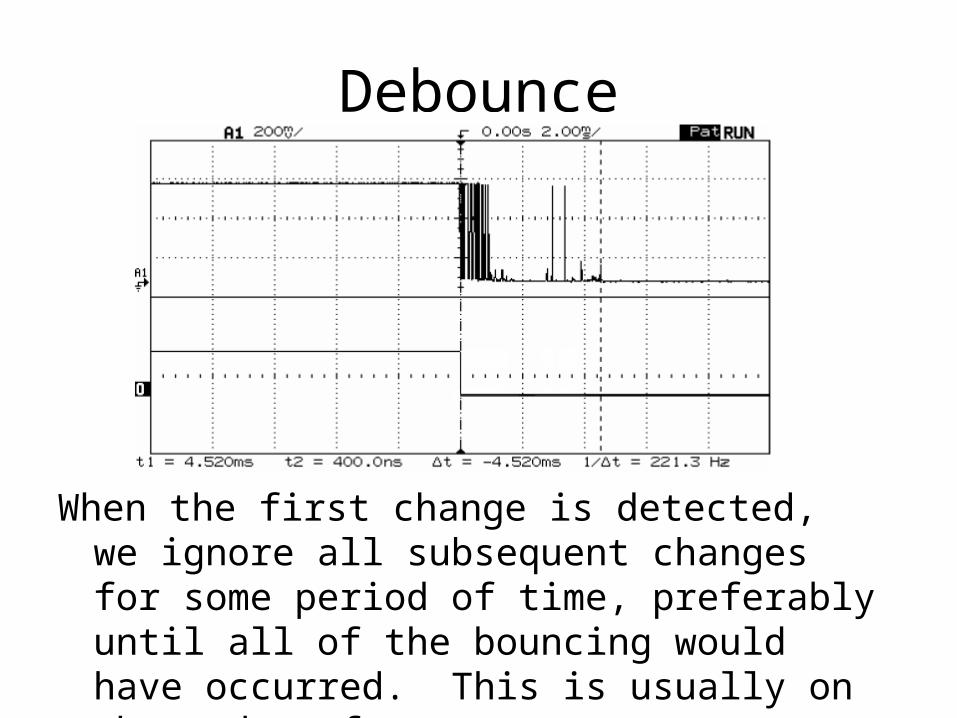
Debounce
When the first change is detected, we ignore all subsequent changes for some period of time, preferably until all of the bouncing would have occurred. This is usually on the order of ms.
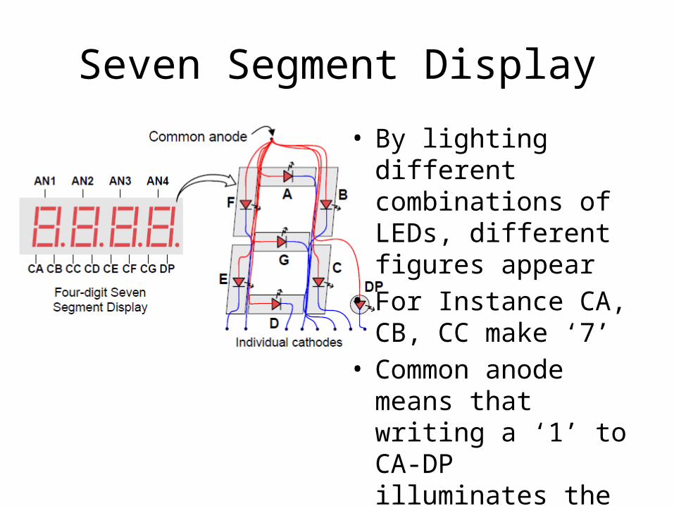
Seven Segment Display
• By lighting different combinations of LEDs, different figures appear
• For Instance CA, CB, CC make ‘7’
• Common anode means that writing a ‘1’ to CA-DP illuminates the led, where a ‘0’ turns it off
Seven Segment Display
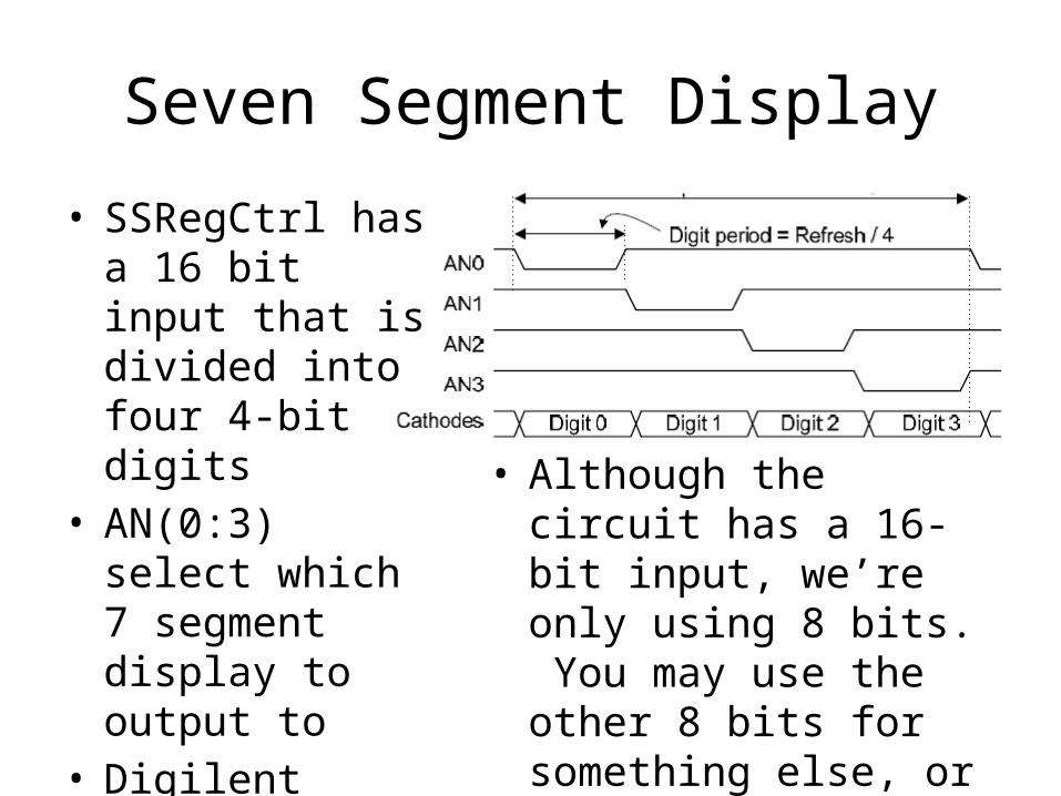
• SSRegCtrl has a 16 bit input that is divided into four 4-bit digits
• AN(0:3) select which 7 segment display to output to
• Digilent recommends a digit period of between 1khz and 60hz
• Although the circuit has a 16-bit input, we’re only using 8 bits. You may use the other 8 bits for something else, or just set them to ‘0’s
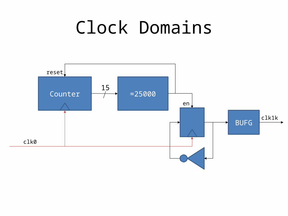
Clock Domains
Counter =2500015
reset
en
clk0
BUFGclk1k
Part 4
User Constraint File (UCF)
User Constraint File (UCF)
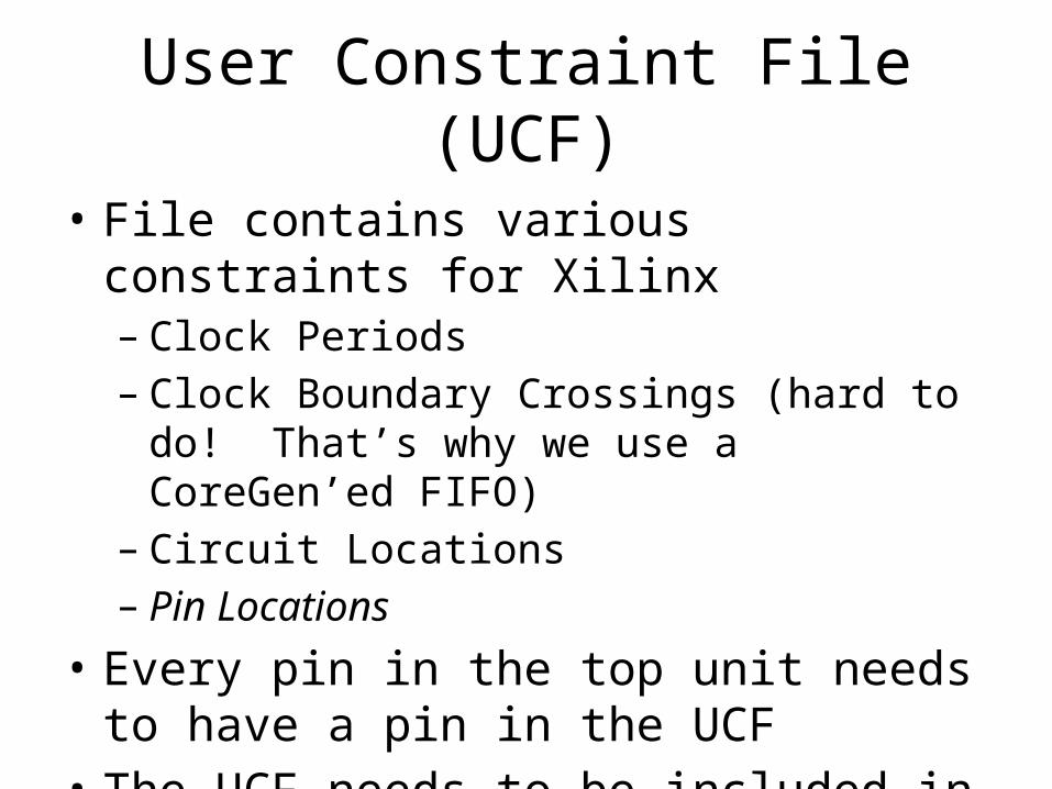
• File contains various constraints for Xilinx– Clock Periods– Clock Boundary Crossings (hard to do! That’s why
we use a CoreGen’ed FIFO)– Circuit Locations– Pin Locations
• Every pin in the top unit needs to have a pin in the UCF
• The UCF needs to be included in Xilinx ISE, but not simulator (i.e. Aldec)
User Constraint File (UCF)
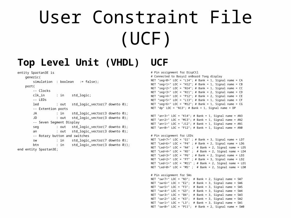
Top Level Unit (VHDL)entity Spartan3E is generic( simulation : boolean := false); port( -- Clocks clk_in : in std_logic; -- LEDs led : out std_logic_vector(7 downto 0); -- Extention ports JA : in std_logic_vector(3 downto 0); JD : out std_logic_vector(3 downto 0); -- Seven Segment Display seg : out std_logic_vector(7 downto 0); an : out std_logic_vector(3 downto 0); -- Rotary button and switches sw : in std_logic_vector(7 downto 0); btn : in std_logic_vector(3 downto 0));end entity Spartan3E;
UCF# Pin assignment for DispCtl# Connected to Basys2 onBoard 7seg displayNET "seg<0>" LOC = "L14"; # Bank = 1, Signal name = CANET "seg<1>" LOC = "H12"; # Bank = 1, Signal name = CBNET "seg<2>" LOC = "N14"; # Bank = 1, Signal name = CCNET "seg<3>" LOC = "N11"; # Bank = 2, Signal name = CDNET "seg<4>" LOC = "P12"; # Bank = 2, Signal name = CENET "seg<5>" LOC = "L13"; # Bank = 1, Signal name = CFNET "seg<6>" LOC = "M12"; # Bank = 1, Signal name = CGNET "dp" LOC = "N13"; # Bank = 1, Signal name = DP
NET "an<3>" LOC = "K14"; # Bank = 1, Signal name = AN3NET "an<2>" LOC = "M13"; # Bank = 1, Signal name = AN2NET "an<1>" LOC = "J12"; # Bank = 1, Signal name = AN1NET "an<0>" LOC = "F12"; # Bank = 1, Signal name = AN0
# Pin assignment for LEDsNET "Led<7>" LOC = "G1" ; # Bank = 3, Signal name = LD7NET "Led<6>" LOC = "P4" ; # Bank = 2, Signal name = LD6NET "Led<5>" LOC = "N4" ; # Bank = 2, Signal name = LD5NET "Led<4>" LOC = "N5" ; # Bank = 2, Signal name = LD4NET "Led<3>" LOC = "P6" ; # Bank = 2, Signal name = LD3NET "Led<2>" LOC = "P7" ; # Bank = 3, Signal name = LD2NET "Led<1>" LOC = "M11" ; # Bank = 2, Signal name = LD1NET "Led<0>" LOC = "M5" ; # Bank = 2, Signal name = LD0
# Pin assignment for SWsNET "sw<7>" LOC = "N3"; # Bank = 2, Signal name = SW7NET "sw<6>" LOC = "E2"; # Bank = 3, Signal name = SW6NET "sw<5>" LOC = "F3"; # Bank = 3, Signal name = SW5NET "sw<4>" LOC = "G3"; # Bank = 3, Signal name = SW4NET "sw<3>" LOC = "B4"; # Bank = 3, Signal name = SW3NET "sw<2>" LOC = "K3"; # Bank = 3, Signal name = SW2NET "sw<1>" LOC = "L3"; # Bank = 3, Signal name = SW1NET "sw<0>" LOC = "P11"; # Bank = 2, Signal name = SW0
Part 5
CoreGen
Part 6
Board Demonstration
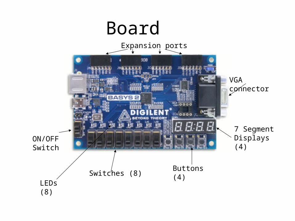
Board
Switches (8)Buttons (4)
7 Segment Displays (4)
VGA connector
ON/OFF Switch
Expansion ports
LEDs (8)
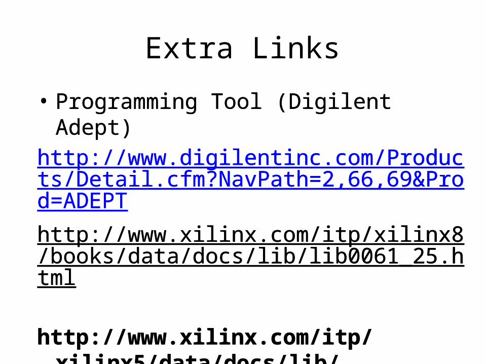
Extra Links
• Programming Tool (Digilent Adept)http://www.digilentinc.com/Products/Detail.cfm?NavPath=2,66,69&Prod=ADEPThttp://www.xilinx.com/itp/xilinx8/books/data/docs/lib/lib0061_25.html
http://www.xilinx.com/itp/xilinx5/data/docs/
lib/lib0233_217.html
• Programming Tool (Digilent Adept)http://www.digilentinc.com/Products/Detail.cfm?NavPath=2,66,69&Prod=ADEPThttp://www.xilinx.com/itp/xilinx8/books/data/docs/lib/lib0061_25.html
http://www.xilinx.com/itp/xilinx5/data/docs/
lib/lib0233_217.html