Embed Size (px)
DESCRIPTION
ECE 448 Lab 1 Developing Effective Testbenches. ECE 44 8 – FPGA and ASIC Design with VHDL. George Mason University. Agenda for today. Part 1: Refresher on Simple Testbenches Part 2: Hands-on Session: ISim & Templates Part 3: More Advanced Testbenches Part 4: Lab Exercise 1 - PowerPoint PPT Presentation
Citation preview
George Mason UniversityECE 448 – FPGA and ASIC Design with VHDL George Mason University
ECE 448
Lab 1
Developing Effective
Testbenches

2
Part 1: Refresher on Simple Testbenches
Part 2: Hands-on Session: ISim & Templates
Part 3: More Advanced Testbenches
Part 4: Lab Exercise 1
Part 5: Lab Exercise 2
Part 6: Introduction to Lab 1
Agenda for today
3ECE 448 – FPGA and ASIC Design with VHDL
Part 1
Refresher on VHDL Testbenches

4ECE 448 – FPGA and ASIC Design with VHDL
Simple Testbench
Processes
Generating
Stimuli
Design Under Test (DUT)
Observed Outputs
5ECE 448 – FPGA and ASIC Design with VHDL
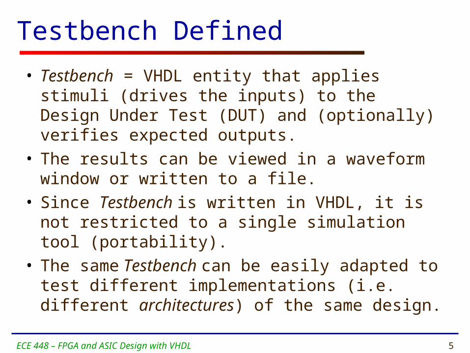
Testbench Defined
• Testbench = VHDL entity that applies stimuli (drives the inputs) to the Design Under Test (DUT) and (optionally) verifies expected outputs.
• The results can be viewed in a waveform window or written to a file.
• Since Testbench is written in VHDL, it is not restricted to a single simulation tool (portability).
• The same Testbench can be easily adapted to test different implementations (i.e. different architectures) of the same design.

6ECE 448 – FPGA and ASIC Design with VHDL
Representative
Inputs
VHDL Design
Manual Calculations
or
Reference Software
Implementation(C, Java, Matlab )
expected results
Testbench
actual results= ?
Possible sources of expected results used for comparison

7ECE 448 – FPGA and ASIC Design with VHDL
Test vectors
Set of pairs: {Input Values i, Expected Outputs Values i}
Input Values 1, Expected Output Values 1
Input Values 2, Expected Output Values 2
……………………………
Input Values N, Expected Output Values N
Test vectors can cover either:
- all combinations of inputs (for very simple circuits only)
- selected representative combinations of inputs
(most realistic circuits)
8ECE 448 – FPGA and ASIC Design with VHDL
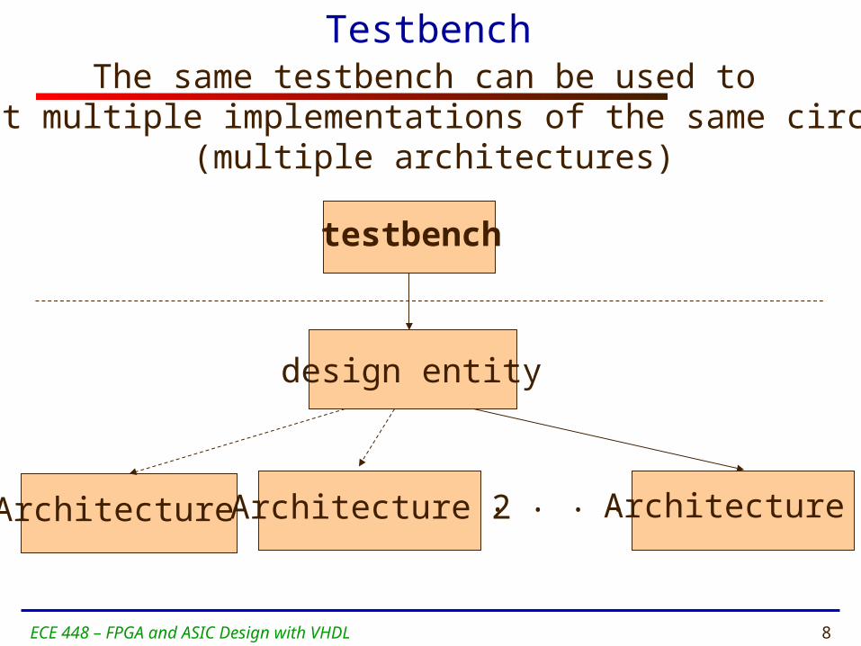
Testbench
testbench
design entity
Architecture 1 Architecture 2 Architecture N. . . .
The same testbench can be used to test multiple implementations of the same circuit
(multiple architectures)
9ECE 448 – FPGA and ASIC Design with VHDL
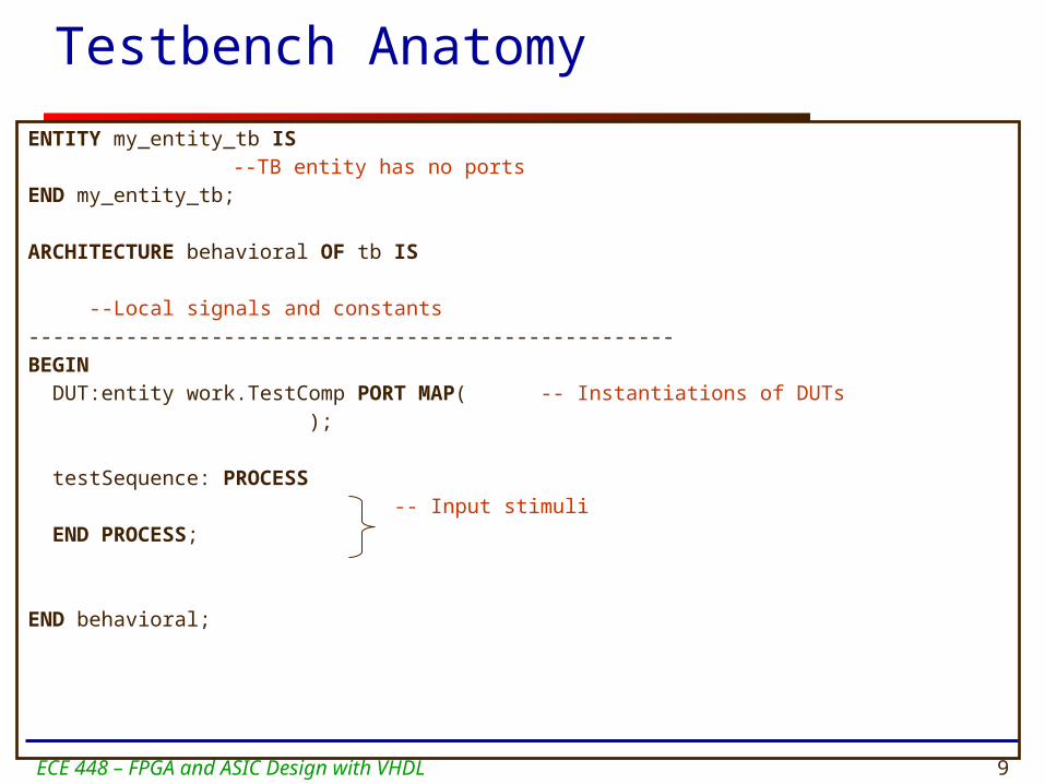
Testbench Anatomy
ENTITY my_entity_tb IS --TB entity has no ports
END my_entity_tb;
ARCHITECTURE behavioral OF tb IS
--Local signals and constants-----------------------------------------------------BEGIN DUT:entity work.TestComp PORT MAP( -- Instantiations of DUTs ); testSequence: PROCESS -- Input stimuli END PROCESS;
END behavioral;

10ECE 448 – FPGA and ASIC Design with VHDL
Testbench for XOR3 (1)
LIBRARY ieee;USE ieee.std_logic_1164.all;
ENTITY xor3_tb ISEND xor3_tb;
ARCHITECTURE behavioral OF xor3_tb IS
-- Stimulus signals - signals mapped to the input and inout ports of tested entitySIGNAL test_vector: STD_LOGIC_VECTOR(2 DOWNTO 0);SIGNAL test_result : STD_LOGIC;

11ECE 448 – FPGA and ASIC Design with VHDL
Testbench for XOR3 (2)
BEGINUUT : entity work.xor3
PORT MAP (A => test_vector(2),B => test_vector(1),C => test_vector(0),Result => test_result);
); Testing: PROCESS BEGIN test_vector <= "000";
WAIT FOR 10 ns; test_vector <= "001"; WAIT FOR 10 ns; test_vector <= "010"; WAIT FOR 10 ns;
test_vector <= "011"; WAIT FOR 10 ns; test_vector <= "100"; WAIT FOR 10 ns; test_vector <= "101"; WAIT FOR 10 ns; test_vector <= "110"; WAIT FOR 10 ns; test_vector <= "111";
WAIT FOR 10 ns; END PROCESS;END behavioral;

12ECE 448 – FPGA and ASIC Design with VHDL
VHDL Design Styles
Components andinterconnects
structural
VHDL Design Styles
dataflow
Concurrent statements
behavioral
• Testbenches
Sequential statements
13ECE 448 – FPGA and ASIC Design with VHDL
Process without Sensitivity List
and its use in Testbenches
14ECE 448 – FPGA and ASIC Design with VHDL
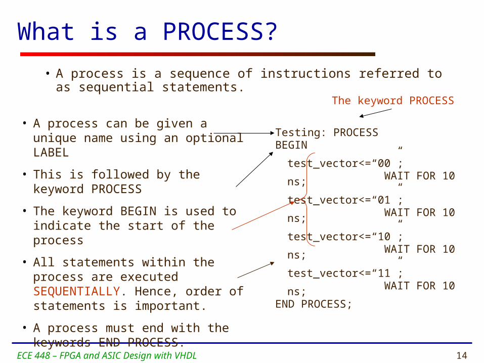
• A process can be given a unique name using an optional LABEL
• This is followed by the keyword PROCESS
• The keyword BEGIN is used to indicate the start of the process
• All statements within the process are executed SEQUENTIALLY. Hence, order of statements is important.
• A process must end with the keywords END PROCESS.
Testing: PROCESS BEGIN
test_vector<=“00”;WAIT FOR 10 ns;
test_vector<=“01”;WAIT FOR 10 ns;
test_vector<=“10”;WAIT FOR 10 ns;
test_vector<=“11”;WAIT FOR 10 ns;
END PROCESS;
• A process is a sequence of instructions referred to as sequential statements.
What is a PROCESS?
The keyword PROCESS
15ECE 448 – FPGA and ASIC Design with VHDL
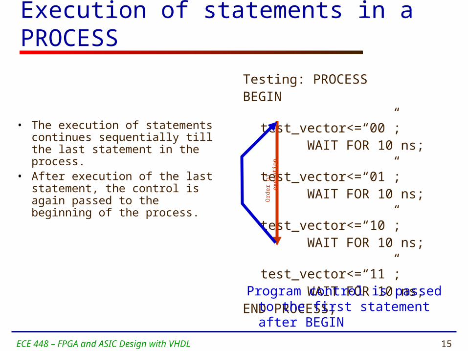
Execution of statements in a PROCESS
• The execution of statements continues sequentially till the last statement in the process.
• After execution of the last statement, the control is again passed to the beginning of the process.
Testing: PROCESS BEGIN
test_vector<=“00”;WAIT FOR 10 ns;test_vector<=“01”;WAIT FOR 10 ns;test_vector<=“10”;WAIT FOR 10 ns;test_vector<=“11”;WAIT FOR 10 ns;
END PROCESS;O
rde
r o
f exe
cutio
n
Program control is passed to the first statement after BEGIN

16ECE 448 – FPGA and ASIC Design with VHDL
PROCESS with a WAIT Statement
• The last statement in the PROCESS is a WAIT instead of WAIT FOR 10 ns.
• This will cause the PROCESS to suspend indefinitely when the WAIT statement is executed.
• This form of WAIT can be used in a process included in a testbench when all possible combinations of inputs have been tested or a non-periodical signal has to be generated.
Testing: PROCESSBEGIN
test_vector<=“00”;WAIT FOR 10 ns;test_vector<=“01”;WAIT FOR 10 ns;test_vector<=“10”;WAIT FOR 10 ns;test_vector<=“11”;WAIT;
END PROCESS;
Program execution stops here
Ord
er
of e
xecu
tion

17ECE 448 – FPGA and ASIC Design with VHDL
WAIT FOR vs. WAIT
WAIT FOR: waveform will keep repeating itself forever
WAIT : waveform will keep its state after the last wait instruction.
0 1 2 3
…
0 1 2 3 …

18ECE 448 – FPGA and ASIC Design with VHDL
Specifying time in VHDL
19ECE 448 – FPGA and ASIC Design with VHDL
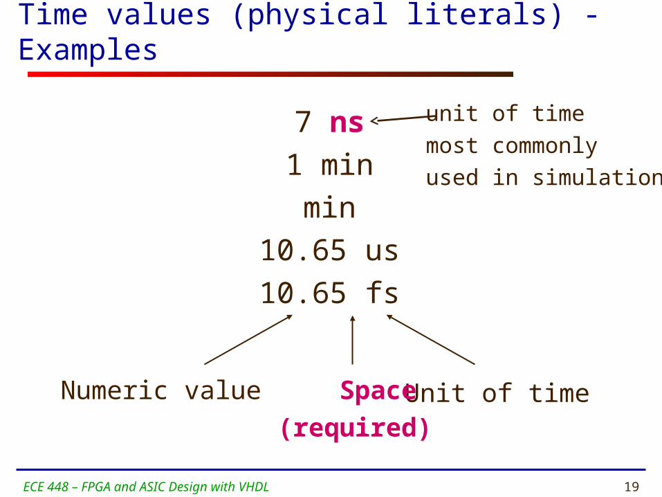
Time values (physical literals) - Examples
7 ns
1 min
min
10.65 us
10.65 fs
Unit of time Space
(required)
Numeric value
unit of time
most commonly
used in simulation

20ECE 448 – FPGA and ASIC Design with VHDL
Units of time
Unit Definition
Base Unit
fs femtoseconds (10-15 seconds)
Derived Units
ps picoseconds (10-12 seconds)
ns nanoseconds (10-9 seconds)
us microseconds (10-6 seconds)
ms miliseconds (10-3 seconds)
sec seconds
min minutes (60 seconds)
hr hours (3600 seconds)
21ECE 448 – FPGA and ASIC Design with VHDL
Simple Testbenches

22ECE 448 – FPGA and ASIC Design with VHDL
Generating selected values of one input
SIGNAL test_vector : STD_LOGIC_VECTOR(2 downto 0);
BEGIN
.......testing: PROCESS
BEGIN
test_vector <= "000";
WAIT FOR 10 ns;
test_vector <= "001";
WAIT FOR 10 ns;
test_vector <= "010";
WAIT FOR 10 ns;
test_vector <= "011";
WAIT FOR 10 ns;
test_vector <= "100";
WAIT FOR 10 ns;
END PROCESS;
........
END behavioral;

23ECE 448 – FPGA and ASIC Design with VHDL
Generating all values of one input
USE ieee.std_logic_unsigned.all;
.......
SIGNAL test_vector : STD_LOGIC_VECTOR(3 downto 0):="0000";
BEGIN
.......
testing: PROCESS
BEGIN
WAIT FOR 10 ns;
test_vector <= test_vector + 1;
end process TESTING;
........
END behavioral;
24ECE 448 – FPGA and ASIC Design with VHDL
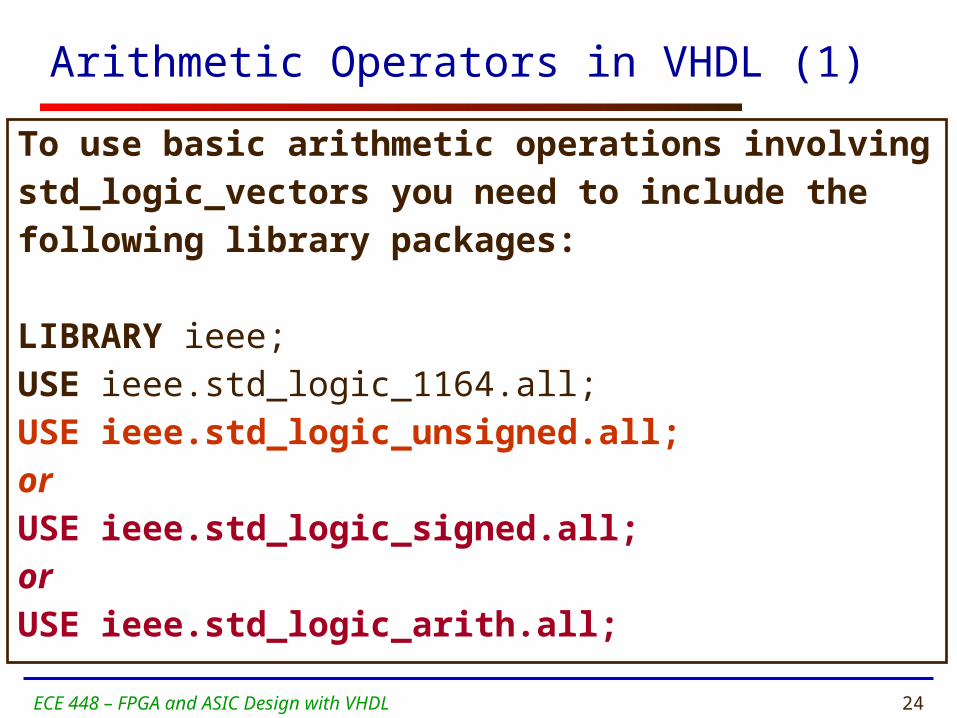
Arithmetic Operators in VHDL (1)
To use basic arithmetic operations involving std_logic_vectors you need to include thefollowing library packages:
LIBRARY ieee;USE ieee.std_logic_1164.all;USE ieee.std_logic_unsigned.all;orUSE ieee.std_logic_signed.all;orUSE ieee.std_logic_arith.all;

25ECE 448 – FPGA and ASIC Design with VHDL
Arithmetic Operators in VHDL (2)
You can use standard +, - operatorsto perform addition and subtraction:
signal A : STD_LOGIC_VECTOR(3 downto 0); signal B : STD_LOGIC_VECTOR(3 downto 0); signal C : STD_LOGIC_VECTOR(3 downto 0);
…… C <= A + B;

26ECE 448 – FPGA and ASIC Design with VHDL
Different ways of performing the same operation
signal count: std_logic_vector(7 downto 0);
You can use:
count <= count + “00000001”;
or
count <= count + 1;
or
count <= count + ‘1’;

27ECE 448 – FPGA and ASIC Design with VHDL
Different declarations for the same operator
Declarations in the package ieee.std_logic_unsigned:
function “+” ( L: std_logic_vector; R: std_logic_vector)
return std_logic_vector;
function “+” ( L: std_logic_vector; R: integer)
return std_logic_vector;
function “+” ( L: std_logic_vector; R: std_logic)
return std_logic_vector;
28ECE 448 – FPGA and ASIC Design with VHDL
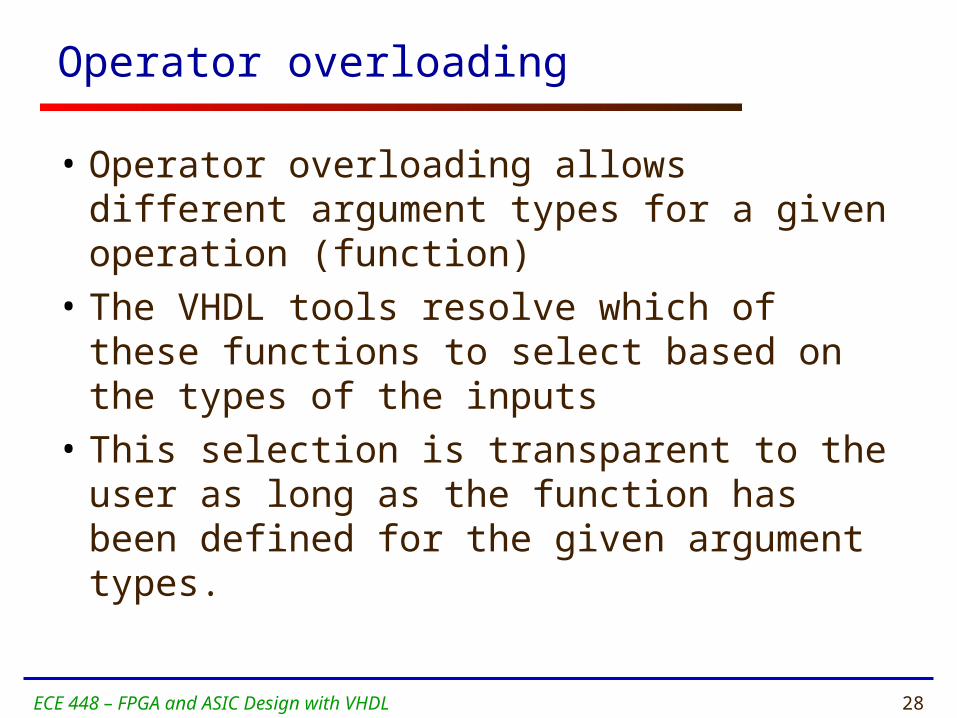
Operator overloading
• Operator overloading allows different argument types for a given operation (function)
• The VHDL tools resolve which of these functions to select based on the types of the inputs
• This selection is transparent to the user as long as the function has been defined for the given argument types.
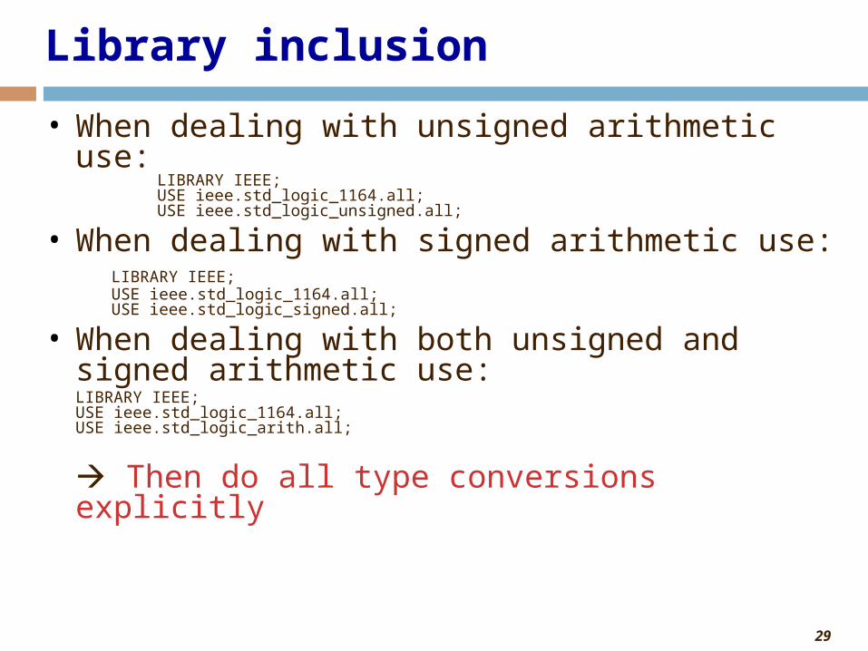
29
Library inclusion
• When dealing with unsigned arithmetic use:LIBRARY IEEE;USE ieee.std_logic_1164.all;USE ieee.std_logic_unsigned.all;
• When dealing with signed arithmetic use:LIBRARY IEEE;USE ieee.std_logic_1164.all;USE ieee.std_logic_signed.all;
• When dealing with both unsigned and signed arithmetic use:LIBRARY IEEE;USE ieee.std_logic_1164.all;USE ieee.std_logic_arith.all;
Then do all type conversions explicitly

30
std_logic_unsigned vs. std_logic_arith
library IEEE;
use IEEE.STD_LOGIC_1164.all;
use IEEE.std_logic_arith.all;
entity adder is
port(
a : in STD_LOGIC_VECTOR(2 downto 0);
b : in STD_LOGIC_VECTOR(2 downto 0);
c : out STD_LOGIC_VECTOR(2 downto 0) );
end adder;
architecture adder_arch of adder is
begin
c <= std_logic_vector(unsigned(a) + unsigned(b));
end adder_arch;
library IEEE;
use IEEE.STD_LOGIC_1164.all;
use IEEE.std_logic_unsigned.all;
entity adder is
port(
a : in STD_LOGIC_VECTOR(2 downto 0);
b : in STD_LOGIC_VECTOR(2 downto 0);
c : out STD_LOGIC_VECTOR(2 downto 0) );
end adder;
architecture adder_arch of adder is
begin
c <= a + b;
end adder_arch;
UNSIGNED ADDER WITH NO CARRYOUT
Tells compiler totreat std_logic_vectorlike unsigned type

31
std_logic_signed vs. std_logic_arith
library IEEE;
use IEEE.STD_LOGIC_1164.all;
use IEEE.std_logic_arith.all;
entity adder is
port(
a : in STD_LOGIC_VECTOR(2 downto 0);
b : in STD_LOGIC_VECTOR(2 downto 0);
c : out STD_LOGIC_VECTOR(2 downto 0) );
end adder;
architecture adder_arch of adder is
begin
c <= std_logic_vector(signed(a) + signed(b));
end adder_arch;
library IEEE;
use IEEE.STD_LOGIC_1164.all;
use IEEE.std_logic_signed.all;
entity adder is
port(
a : in STD_LOGIC_VECTOR(2 downto 0);
b : in STD_LOGIC_VECTOR(2 downto 0);
c : out STD_LOGIC_VECTOR(2 downto 0) );
end adder;
architecture adder_arch of adder is
begin
c <= a + b;
end adder_arch;
SIGNED ADDER
Tells compiler totreat std_logic_vectorlike signed type

32ECE 448 – FPGA and ASIC Design with VHDL
USE ieee.std_logic_unsigned.all;
...........
SIGNAL test_ab : STD_LOGIC_VECTOR(1 downto 0);
SIGNAL test_sel : STD_LOGIC_VECTOR(1 downto 0);BEGIN
.......double_loop: PROCESSBEGIN
test_ab <="00";test_sel <="00";for I in 0 to 3 loop for J in 0 to 3 loop
wait for 10 ns;test_ab <= test_ab + 1;
end loop; test_sel <= test_sel + 1;end loop;
END PROCESS;
........
END behavioral;
Generating all possible values of two inputs

33ECE 448 – FPGA and ASIC Design with VHDL
Generating periodical signals, such as clocks
CONSTANT clk1_period : TIME := 20 ns;
CONSTANT clk2_period : TIME := 200 ns;
SIGNAL clk1 : STD_LOGIC;
SIGNAL clk2 : STD_LOGIC := ‘0’;
BEGIN
.......
clk1_generator: PROCESS
clk1 <= ‘0’;
WAIT FOR clk1_period/2;
clk1 <= ‘1’;
WAIT FOR clk1_period/2;
END PROCESS;
clk2 <= not clk2 after clk2_period/2;
.......
END behavioral;

34ECE 448 – FPGA and ASIC Design with VHDL
Generating one-time signals, such as resets
CONSTANT reset1_width : TIME := 100 ns;
CONSTANT reset2_width : TIME := 150 ns;
SIGNAL reset1 : STD_LOGIC;
SIGNAL reset2 : STD_LOGIC := ‘1’;
BEGIN
.......
reset1_generator: PROCESS
reset1 <= ‘1’;
WAIT FOR reset1_width;
reset1 <= ‘0’;
WAIT;
END PROCESS;
reset2_generator: PROCESS
WAIT FOR reset2_width;
reset2 <= ‘0’;
WAIT;
END PROCESS;
.......
END behavioral;

35ECE 448 – FPGA and ASIC Design with VHDL
Typical error
SIGNAL test_vector : STD_LOGIC_VECTOR(2 downto 0);
SIGNAL reset : STD_LOGIC;
BEGIN
.......
generator1: PROCESS
reset <= ‘1’;
WAIT FOR 100 ns
reset <= ‘0’;
test_vector <="000";
WAIT;
END PROCESS;
generator2: PROCESS
WAIT FOR 200 ns
test_vector <="001";
WAIT FOR 600 ns
test_vector <="011";
END PROCESS;
.......
END behavioral;

36
Example of Design Under Test
B
A
NEG_A
NEG_B
IN0
IN1
IN2
IN3
OUTPUT
SEL1SEL0
MUX_4_1
L0L1
NEG_Y
Y
Y1
A1
B1
MUX_0
MUX_1
MUX_2
MUX_3
0
1
0
1
0
1
Example 1
Simple Testbench
MLU_tb.vhd

38ECE 448 – FPGA and ASIC Design with VHDL
Part 2
Hands-on Session:
Simulation using ISim
Use of VHDL Templates
39ECE 448 – FPGA and ASIC Design with VHDL
Part 3
More Advanced Testbenches

40
More Advanced Testbenches
Processes
Generating
Input
Stimuli
Design Under Test (DUT)
Process
Comparing
Actual Outputs
vs.
Expected Outputs
Design
Correct/Incorrect
Yes/No

41ECE 448 – FPGA and ASIC Design with VHDL
Records
42
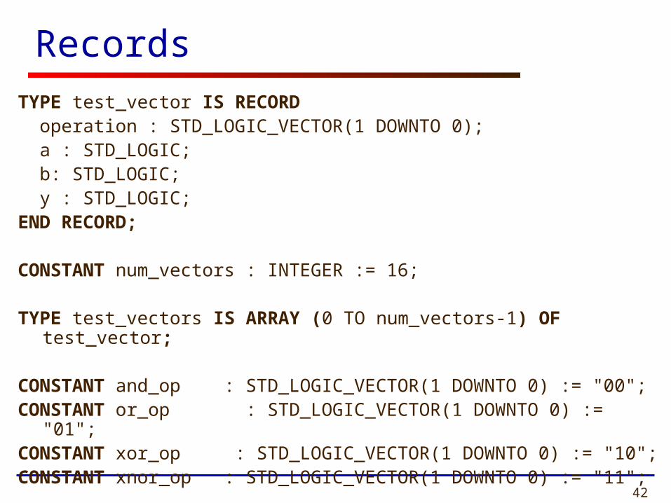
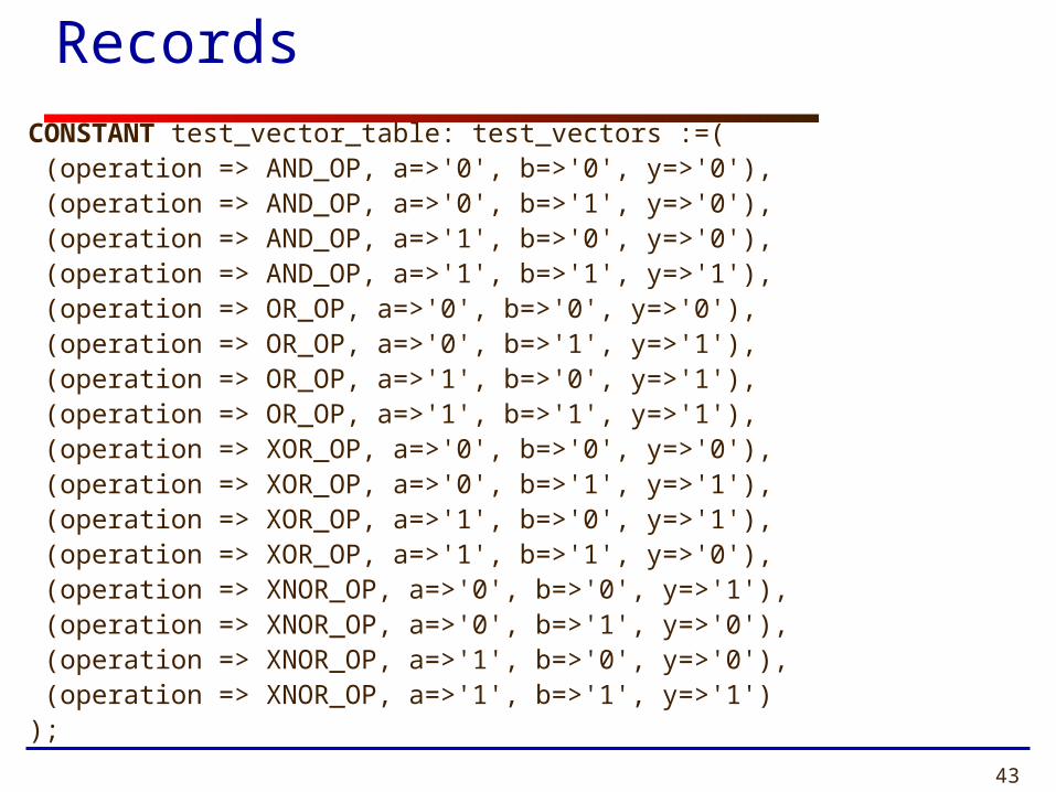
Records
TYPE test_vector IS RECORD operation : STD_LOGIC_VECTOR(1 DOWNTO 0); a : STD_LOGIC; b: STD_LOGIC; y : STD_LOGIC;END RECORD;
CONSTANT num_vectors : INTEGER := 16;
TYPE test_vectors IS ARRAY (0 TO num_vectors-1) OF test_vector;
CONSTANT and_op : STD_LOGIC_VECTOR(1 DOWNTO 0) := "00";CONSTANT or_op : STD_LOGIC_VECTOR(1 DOWNTO 0) := "01";CONSTANT xor_op : STD_LOGIC_VECTOR(1 DOWNTO 0) := "10";CONSTANT xnor_op : STD_LOGIC_VECTOR(1 DOWNTO 0) := "11";
43
RecordsCONSTANT test_vector_table: test_vectors :=( (operation => AND_OP, a=>'0', b=>'0', y=>'0'), (operation => AND_OP, a=>'0', b=>'1', y=>'0'), (operation => AND_OP, a=>'1', b=>'0', y=>'0'), (operation => AND_OP, a=>'1', b=>'1', y=>'1'), (operation => OR_OP, a=>'0', b=>'0', y=>'0'), (operation => OR_OP, a=>'0', b=>'1', y=>'1'), (operation => OR_OP, a=>'1', b=>'0', y=>'1'), (operation => OR_OP, a=>'1', b=>'1', y=>'1'), (operation => XOR_OP, a=>'0', b=>'0', y=>'0'), (operation => XOR_OP, a=>'0', b=>'1', y=>'1'), (operation => XOR_OP, a=>'1', b=>'0', y=>'1'), (operation => XOR_OP, a=>'1', b=>'1', y=>'0'), (operation => XNOR_OP, a=>'0', b=>'0', y=>'1'), (operation => XNOR_OP, a=>'0', b=>'1', y=>'0'), (operation => XNOR_OP, a=>'1', b=>'0', y=>'0'), (operation => XNOR_OP, a=>'1', b=>'1', y=>'1'));

44ECE 448 – FPGA and ASIC Design with VHDL
Variables

45
Variables - features
• Can only be declared within processes and subprograms (functions & procedures)
• Initial value can be explicitly specified in the declaration
• When assigned take an assigned value immediately
• Variable assignments represent the desired behavior, not the structure of the circuit
• Can be used freely in testbenches• Should be avoided, or at least used with caution
in a synthesizable code

46
Variables - Example
testing: PROCESS
VARIABLE error_cnt: INTEGER := 0;
BEGINFOR i IN 0 to num_vectors-1 LOOP
test_operation <= test_vector_table(i).operation;test_a <= test_vector_table(i).a;test_b <= test_vector_table(i).b;WAIT FOR 10 ns;IF test_y /= test_vector_table(i).y THEN
error_cnt := error_cnt + 1;END IF;
END LOOP;END PROCESS testing;

47ECE 448 – FPGA and ASIC Design with VHDL
Asserts and Reports

48
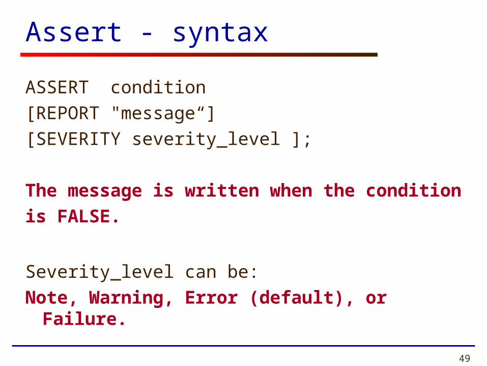
Assert
Assert is a non-synthesizable statement
whose purpose is to write out messages
on the screen when problems are found
during simulation.
Depending on the severity of the problem,
The simulator is instructed to continue
simulation or halt.
49
Assert - syntax
ASSERT condition
[REPORT "message“]
[SEVERITY severity_level ];
The message is written when the condition
is FALSE.
Severity_level can be:
Note, Warning, Error (default), or Failure.

50
Assert – Examples (1)
assert initial_value <= max_value
report "initial value too large"
severity error;
assert packet_length /= 0
report "empty network packet received"
severity warning;
assert false
report "Initialization complete"
severity note;

51
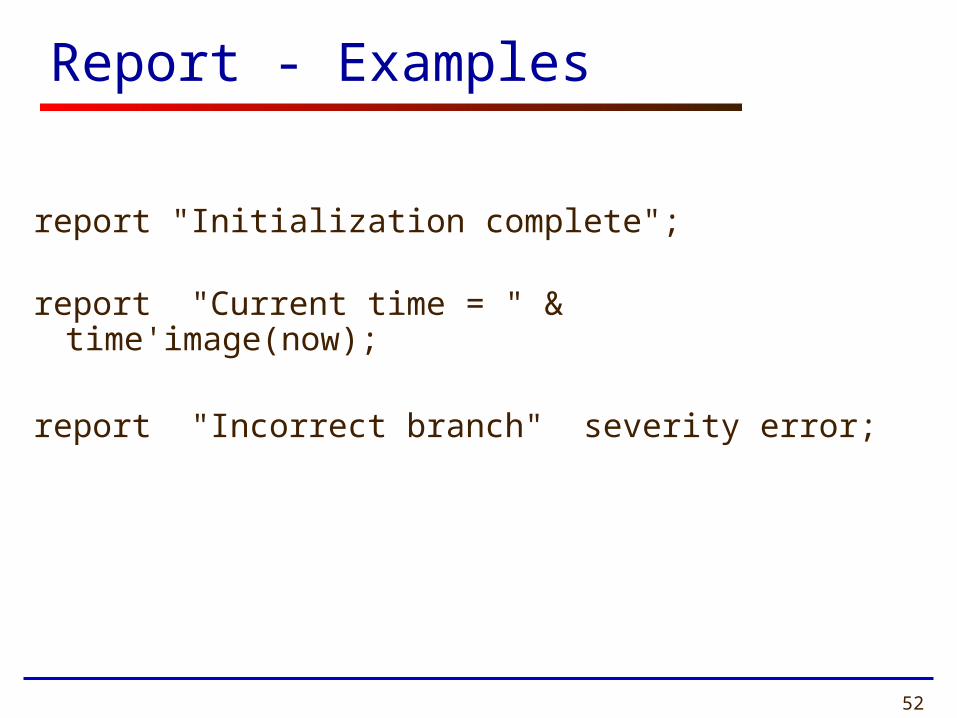
Report - syntax
REPORT "message"
[SEVERITY severity_level ];
The message is always written.
Severity_level can be:
Note (default), Warning, Error, or Failure.
52
Report - Examples
report "Initialization complete";
report "Current time = " & time'image(now);
report "Incorrect branch" severity error;
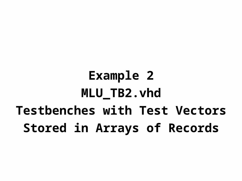
Example 2
MLU_TB2.vhd
Testbenches with Test Vectors
Stored in Arrays of Records
54ECE 448 – FPGA and ASIC Design with VHDL
Part 4
Lab Exercise 1
Testbenches for Combinational Logic
55ECE 448 – FPGA and ASIC Design with VHDL
Part 5
Lab Exercise 2
Testbenches for Sequential Logic
56ECE 448 – FPGA and ASIC Design with VHDL
Part 6
Introduction to Lab 1:
Developing Effective Testbenches
57
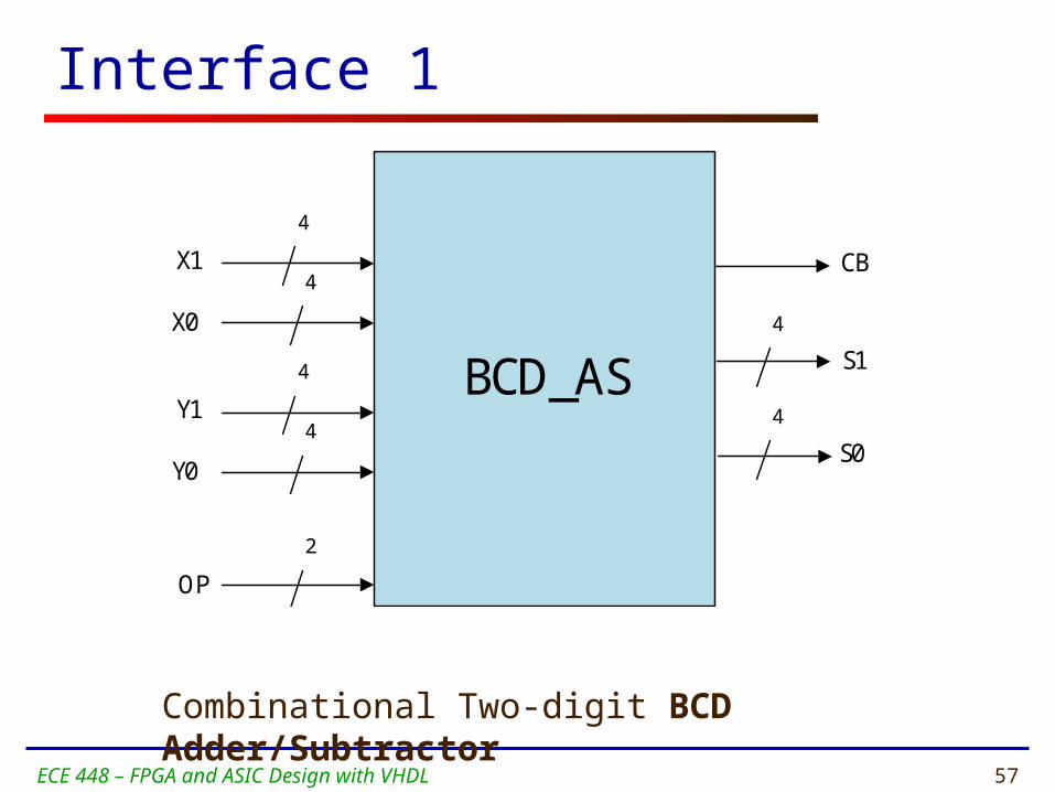
Interface 1
ECE 448 – FPGA and ASIC Design with VHDL
BCD_AS
X1
X0
OP
CB
S1
S0
Y1
Y0
4
4
2
4
4
4
4
Combinational Two-digit BCD Adder/Subtractor
58
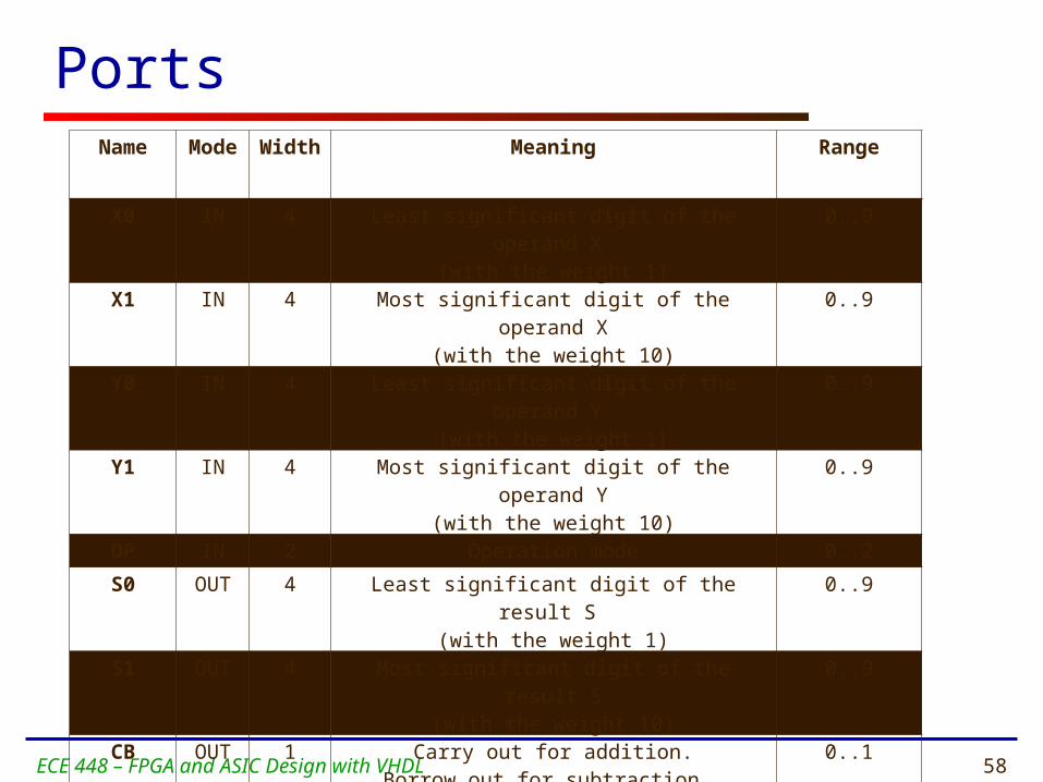
Ports
ECE 448 – FPGA and ASIC Design with VHDL
Name Mode Width Meaning Range
X0 IN 4 Least significant digit of the operand X (with the weight 1)
0..9
X1 IN 4 Most significant digit of the operand X(with the weight 10)
0..9
Y0 IN 4 Least significant digit of the operand Y (with the weight 1)
0..9
Y1 IN 4 Most significant digit of the operand Y(with the weight 10)
0..9
OP IN 2 Operation mode 0..2
S0 OUT 4 Least significant digit of the result S (with the weight 1)
0..9
S1 OUT 4 Most significant digit of the result S(with the weight 10)
0..9
CB OUT 1 Carry out for addition.Borrow out for subtraction.
0..1

59
Interface 2
ECE 448 – FPGA and ASIC Design with VHDL
BCD_AS_SEQ
A
CLK
OP
SEL_OUT
R
RESET
LOAD
SEL_IN
RUN
4
2
2
2
2
Sequential Two-digit BCD Adder/Subtractor

60
Ports
ECE 448 – FPGA and ASIC Design with VHDL
Name Mode Width Meaning Range
CLK IN 1 System clock RESET IN 1 Reset active high
A IN 4 Digit of an operand 0..9LOAD IN 1 Loading value at input A to one of the internal
registers holding X0, X1, Y0, Y1(control signal active for one clock period;
the action takes place at the rising edge of the clock)
SEL_IN IN 2 0: loading register X01: loading register X12: loading register Y03: loading register Y1
0..3
OP IN 2 Operation mode 0..2RUN IN 1 Writing the result to registers holding S0, S1, and
CB (control signal active for one clock period; the action takes place at the rising edge of the clock)
SEL_OUT IN 2 0: R = S01: R = S1
2: R = “000” || CB
R OUT 4 Digit of a result 0..9