Embed Size (px)
Citation preview

ECE 354 ECE 354 –– Computer Computer Systems Lab IISystems Lab II
D/A and A/D Conversion
2
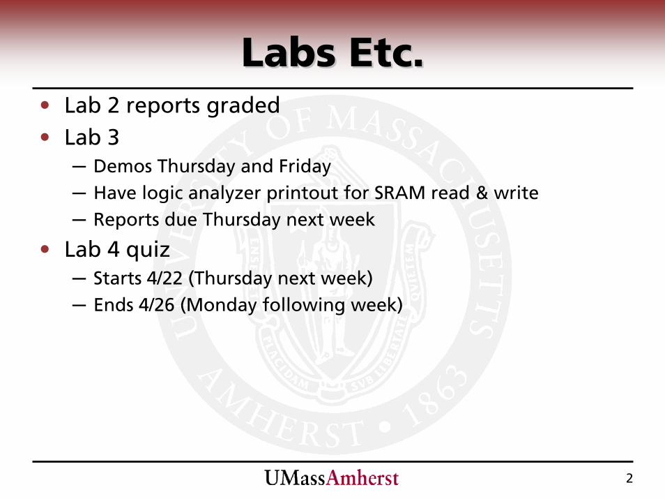
Labs Etc.Labs Etc.• Lab 2 reports graded• Lab 3
Demos Thursday and Friday Have logic analyzer printout for SRAM read & write Reports due Thursday next week
• Lab 4 quiz Starts 4/22 (Thursday next week) Ends 4/26 (Monday following week)

3
Midterm ExamMidterm Exam• Wednesday 4/21, 2:30 in class• Closed Books• Should require more “understanding” than
“memorization” There will be “programming questions” You’ll get the sheet with the PIC instruction set I will not ask what bit 4 of the STATUS register does But I might ask what an interrupt is, how it’s used, and what
registers are involved with it.
• Might contain very simple concepts from Lab 4• 90 minutes

4
Lab 4 OverviewLab 4 Overview• Analog communication between two PICs
Uses A/D and D/A
• Basic functionality Enter character on terminal 1st PIC converts character to analog voltage Analog value transmitted via wire to 2nd PIC 2nd PIC converts voltage back to digital character 2nd PIC displays character on terminal
• Configurable: PIC sends or receives, how many characters (voltage levels) are allowed
low-passfilter
PIC
MA
X23
2
Sender
PIC MA
X232
4kOhm
0.01
uF
CCP1 AN0TxRx .
Receiver

5
Why Analog?Why Analog?• Not everything is digital!
Analog circuits are still necessary
• Physical phenomena are often analog Many sensors are analog (potentiometer, phototransistor,
thermo-sensor, microphone) Many actuators are analog (solenoid, speakers) Some signals need to be processed in analog domain before
conversion to digital (amplification, filtering, linearization)
• Requires conversion between analog and digital domain DAC: digital to analog converter ADC: analog to digital converter PIC has both

6
Digital and Analog ConversionDigital and Analog Conversion• ADC transfer function:
10-bit ADC converter 1024 voltage levels between
0V and VREF
10-bit digital value
• Usually VDD=VREF
• How does D/A and A/D conversion work?

7
D/A ConversionD/A Conversion• How can a digital “value” be converted into a
corresponding analog voltage?
8
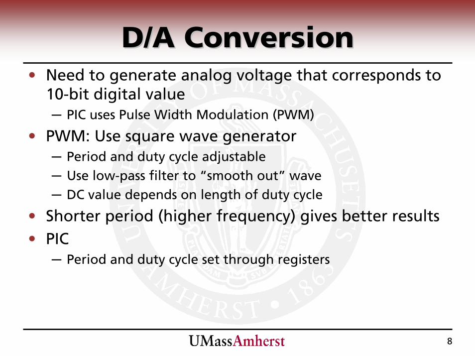
D/A ConversionD/A Conversion• Need to generate analog voltage that corresponds to
10-bit digital value PIC uses Pulse Width Modulation (PWM)
• PWM: Use square wave generator Period and duty cycle adjustable Use low-pass filter to “smooth out” wave DC value depends on length of duty cycle
• Shorter period (higher frequency) gives better results• PIC
Period and duty cycle set through registers

9
Pulse Width ModulationPulse Width Modulation

10
PWM on PICPWM on PIC
• Registers involved: PR2 register: PWM period CCPR1L and CCP1CON<5:4>:
10-bit duty cycle
• Basic operation: Start of period
• Timer TMR2 cleared• CCP1 pin set to high• 10-bit duty cycle latched to
CCPR1H
When TMR2 = CCPR1H• Clear CCP1 (duty cycle over)
When TMR2 = PR2• New period starts

11
CCP1CON RegisterCCP1CON Register

12
Timer 2 Timer 2 PrescalerPrescaler• Prescaler determines
effective clock rate for TMR2
• Postscaler irrelevant for us Used if Timer 2 needs to
drive additional component at different frequency
• PMW period formula:
)2(4]1)2[( prescalerTMRTPRperiodPMW OSC ×××+=

13
PWM Setup PWM Setup • Setup steps:
Set PWM period by writing to PR2 register Set PWM duty cycle by writing to CCPR1L register and
CCP1CON<5:4> bits Make CCP1 pin output by clearing the TRISC<2> bit Set TMR2 prescale value enable Timer 2 by writing to TCON2 Configure the CCP1 module for PWM operation
• Example for 20 MHz clock:

14
A/D ConversionA/D Conversion• How can we generate digital value of analog
voltage?

15
A/D ConversionA/D Conversion• Use D/A converter to generate
different analog values and compare Control logic decides which
values to try When comparison complete, best
match is put on output
• How can D/A be matched to input in fewest steps?
comp
VIN
D/Aconverter
A/D controllogic
10-bit test value
clock
10-bit output
startconversion
conversioncomplete

16
Successive ApproximationSuccessive Approximation• Matching strategies:
Counting conversion (slow) Successive approximation (faster)
• Successive Approximation: Basically binary search: 10 steps instead of
1024
XXX
0XX 1XX
00X 01X 11X10X
000 001 010 011 100 101 110 111
XXX<100?
0XX<010?
1XX<110?
00X<001?
01X<011?
10X<101?
11X<111?

17
PIC ADC Characteristics (1)PIC ADC Characteristics (1)• “Sample and Hold”
ADC samples for a given time (charges hold capacitor) Then sample value is disconnected from source (“hold”) A/D conversion is performed On completion, ADC can sample again
• Sampling takes some time Depends on source impedance (max 10 kΩ) Lower source impedance reduces sample time because hold
capacitance charges faster(see Peatman Figure 10-5(b))
Also depends on temperature, etc.

18
PIC ADC Characteristics (2)PIC ADC Characteristics (2)• Analog input
model and acquisition time formula:

19
ADCON0 RegisterADCON0 Register• ADC enable (bit 0)• Busy/idle (conversion takes some time):
Bit 2 in ADCON0 register Check by polling or enable interrupt
• Channel selection (bits 5-3): Selects pins to be used Selects external or internal reference voltage
• A/D conversion clock setting (bits 7-6)

20
Channel SelectionChannel Selection

21
A/D Conversion Clock SettingA/D Conversion Clock Setting• Time to convert 1 bit must be ≥ 1.6 µs
Clock setting must be adjusted to external clock

22
ADCON1 RegisterADCON1 Register• Port configuration (bits 3-0)
Chooses pins to be digital I/O or analog input (see data sheet)
• Result Format Selection (bit 7) Chooses justification of 10-bit conversion result:

23
ADC SetupADC Setup1. Configure A/D module:
Configure analog pins/voltage reference and digital I/O (ADCON1) Select A/D input channel (ADCON0) Select A/D conversion clock (ADCON0) Turn on A/D module (ADCON0)
2. Configure A/D interrupt (if desired): Clear ADIF bit Set ADIE bit Set PEIE bit Set GIE bit
3. Wait required acquisition time4. Start conversion
Set GO/_DONE bit (ADCON0)5. Wait for A/D conversion to complete (polling or interrupt)6. Read A/D result from (ADRESH:ADRESL) and clear ADIF bit7. Goto 1. or 2. wait 2 A/D clock ticks

24
ReferenceReference• PWM (D/A conversion)
PIC data sheet pp. 61-62 Peatman Section 6.9 (pp. 112-119)
• A/D conversion PIC data sheet pp. 111-116 Peatman Chapter 10

25
Lab 4Lab 4• Lab setup:
2 PICs (available in lab kit) Need 2 terminals
• Send characters coded in analog between terminals• Low pass filter needs to be adapted to PWM settings
low-passfilter
PIC
MA
X23
2
Sender
PIC MA
X232
4kOhm
0.01
uF
CCP1 AN0TxRx .
Receiver

26
Signal Signal DiscretizationDiscretization• We use adaptable signal coding• Choose between 2x (x=1,2,..6) symbols:
• Robustness depends on x: Most robust: only two characters and two voltages
• 512 ADC results can represent one character
Most information: 64 characters and voltage ranges• 16 ADC results can represent one character
0V
VREFB
A
0V
VREF
B
A
22=4symbols
0V
VREF
BA
...
D
C21=2symbols
... 26=64symbols

27
Lab 4 DemoLab 4 Demo• Each PIC can be used for transmitting or receiving
User can specify function after reset
• User also specifies coding level (1..6) Same on both PICs Requires well-designed ASCII manipulation
• When character is entered on terminal PIC 1 receives character Converts it to analog signal PIC 2 received analog signal Converts it to digital value Prints result on terminal
• Should be robust for low coding levels

28
Final CommentsFinal Comments• Questions?