Embed Size (px)
Citation preview
Prof Daniel Holcomb
ECE 353 Lab 3
(Verilog Design Approach)
ECE353: 2 Computer Systems Lab 1 Moritz, Kundu, Holcomb
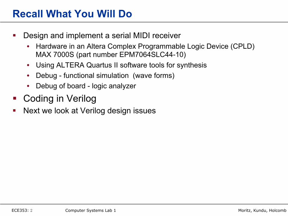
Recall What You Will Do
§ Design and implement a serial MIDI receiver • Hardware in an Altera Complex Programmable Logic Device (CPLD)
MAX 7000S (part number EPM7064SLC44-10) • Using ALTERA Quartus II software tools for synthesis • Debug - functional simulation (wave forms) • Debug of board - logic analyzer
§ Coding in Verilog § Next we look at Verilog design issues
ECE353: 3 Computer Systems Lab 1 Moritz, Kundu, Holcomb
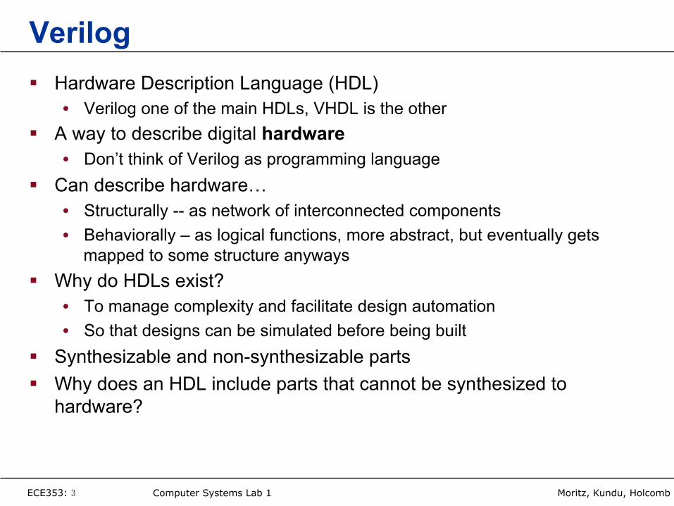
Verilog § Hardware Description Language (HDL)
• Verilog one of the main HDLs, VHDL is the other § A way to describe digital hardware
• Don’t think of Verilog as programming language § Can describe hardware…
• Structurally -- as network of interconnected components • Behaviorally – as logical functions, more abstract, but eventually gets
mapped to some structure anyways § Why do HDLs exist?
• To manage complexity and facilitate design automation • So that designs can be simulated before being built
§ Synthesizable and non-synthesizable parts § Why does an HDL include parts that cannot be synthesized to
hardware?
ECE353: 4 Computer Systems Lab 1 Moritz, Kundu, Holcomb
Hardware Design – Outline § How to Approach the Design Phase § Implementation with Verilog § Requirement for Functional Simulation § Summary
ECE353: 5 Computer Systems Lab 1 Moritz, Kundu, Holcomb
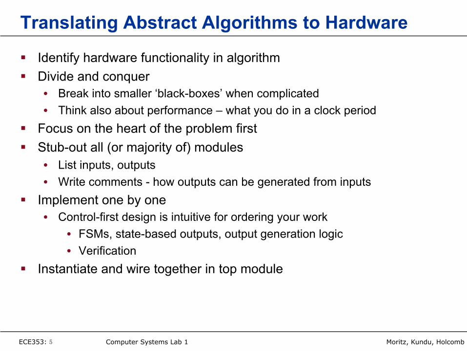
Translating Abstract Algorithms to Hardware
§ Identify hardware functionality in algorithm § Divide and conquer
• Break into smaller ‘black-boxes’ when complicated • Think also about performance – what you do in a clock period
§ Focus on the heart of the problem first § Stub-out all (or majority of) modules
• List inputs, outputs • Write comments - how outputs can be generated from inputs
§ Implement one by one • Control-first design is intuitive for ordering your work
• FSMs, state-based outputs, output generation logic • Verification
§ Instantiate and wire together in top module
ECE353: 6 Computer Systems Lab 1 Moritz, Kundu, Holcomb
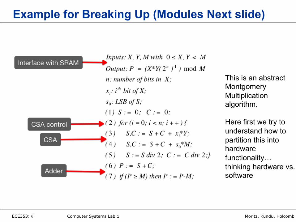
Example for Breaking Up (Modules Next slide)
This is an abstract Montgomery Multiplication algorithm. Here first we try to understand how to partition this into hardware functionality… thinking hardware vs. software
ECE353: 7 Computer Systems Lab 1 Moritz, Kundu, Holcomb
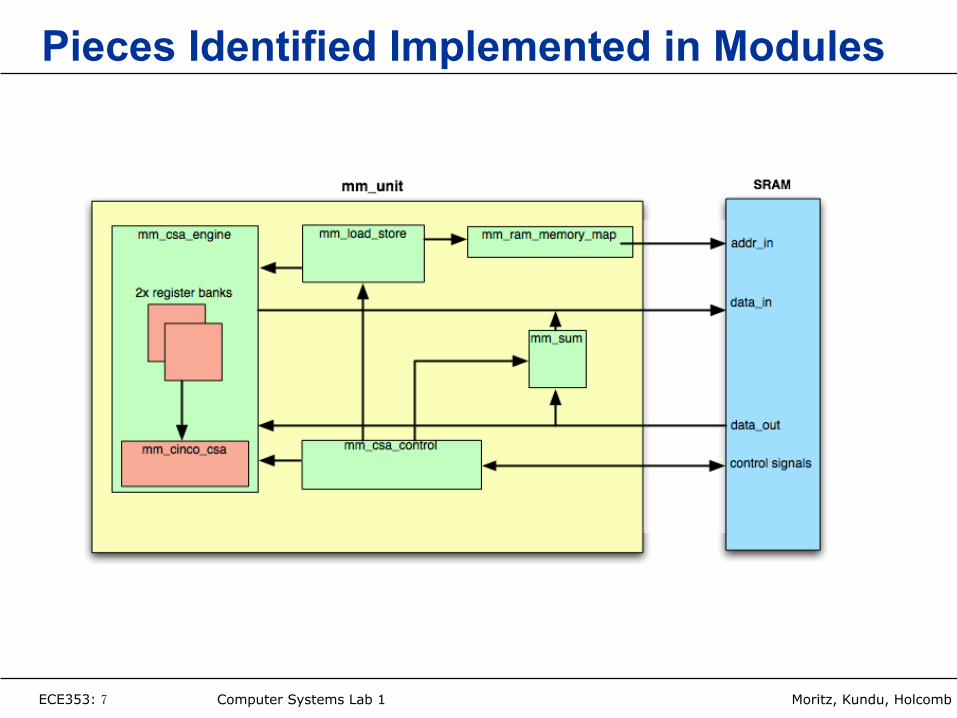
Pieces Identified Implemented in Modules
ECE353: 8 Computer Systems Lab 1 Moritz, Kundu, Holcomb
Hardware Design – Outline § How to Approach Design Phase § Implementation with Verilog § Requirements for Functional Simulation § Summary
ECE353: 9 Computer Systems Lab 1 Moritz, Kundu, Holcomb
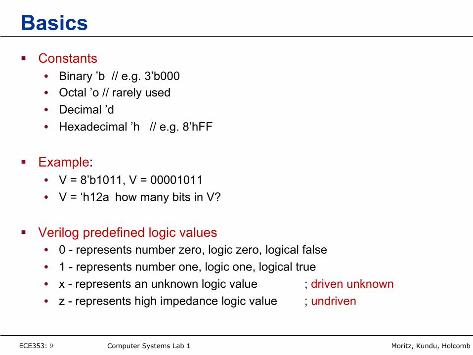
Basics § Constants
• Binary ’b // e.g. 3’b000 • Octal ’o // rarely used • Decimal ’d • Hexadecimal ’h // e.g. 8’hFF
§ Example: • V = 8’b1011, V = 00001011 • V = ‘h12a how many bits in V?
§ Verilog predefined logic values • 0 - represents number zero, logic zero, logical false • 1 - represents number one, logic one, logical true • x - represents an unknown logic value ; driven unknown • z - represents high impedance logic value ; undriven
ECE353: 10 Computer Systems Lab 1 Moritz, Kundu, Holcomb
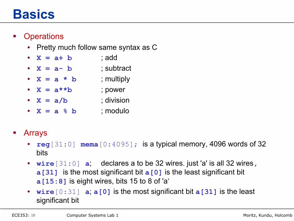
Basics § Operations
• Pretty much follow same syntax as C • X = a+ b ; add • X = a- b ; subtract • X = a * b ; multiply • X = a**b ; power • X = a/b ; division • X = a % b ; modulo
§ Arrays • reg[31:0] mema[0:4095]; is a typical memory, 4096 words of 32
bits • wire[31:0] a; declares a to be 32 wires. just 'a' is all 32 wires,
a[31] is the most significant bit a[0] is the least significant bit a[15:8] is eight wires, bits 15 to 8 of 'a‘
• wire[0:31] a; a[0] is the most significant bit a[31] is the least significant bit
ECE353: 11 Computer Systems Lab 1 Moritz, Kundu, Holcomb
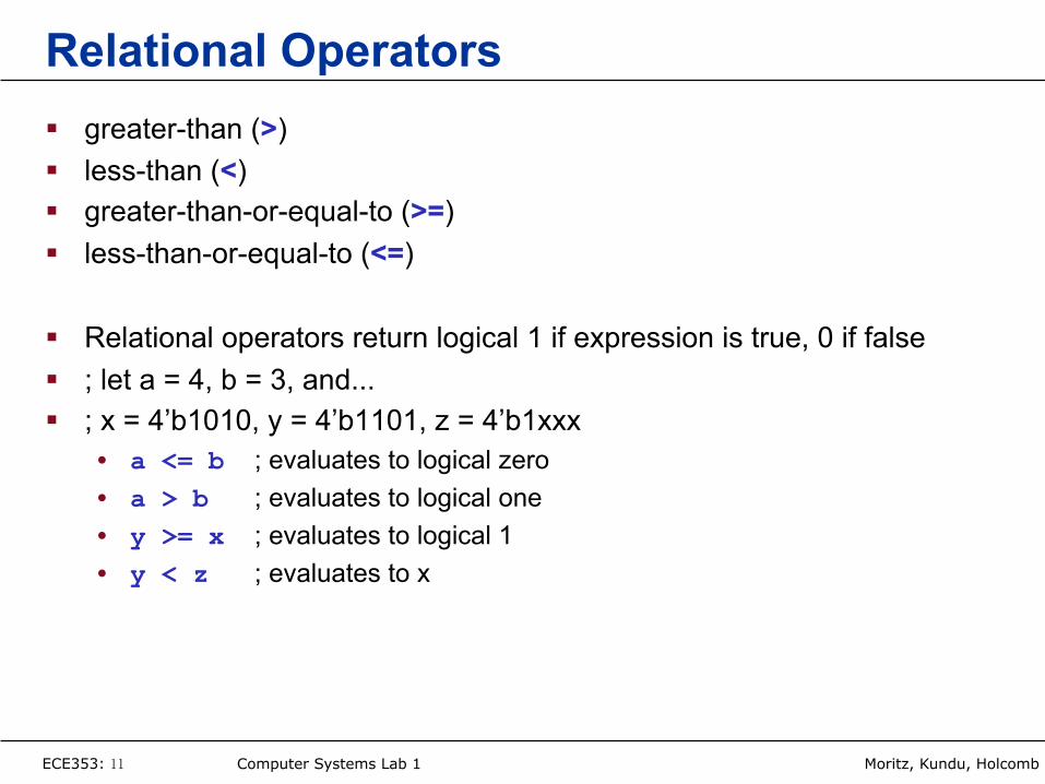
Relational Operators § greater-than (>) § less-than (<) § greater-than-or-equal-to (>=) § less-than-or-equal-to (<=)
§ Relational operators return logical 1 if expression is true, 0 if false § ; let a = 4, b = 3, and... § ; x = 4’b1010, y = 4’b1101, z = 4’b1xxx
• a <= b ; evaluates to logical zero • a > b ; evaluates to logical one • y >= x ; evaluates to logical 1 • y < z ; evaluates to x
ECE353: 12 Computer Systems Lab 1 Moritz, Kundu, Holcomb
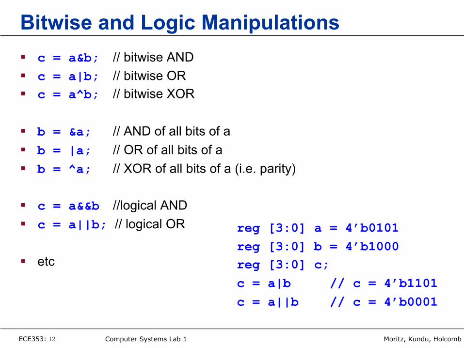
Bitwise and Logic Manipulations § c = a&b; // bitwise AND § c = a|b; // bitwise OR § c = a^b; // bitwise XOR
§ b = &a; // AND of all bits of a § b = |a; // OR of all bits of a § b = ^a; // XOR of all bits of a (i.e. parity)
§ c = a&&b //logical AND § c = a||b; // logical OR
§ etc
reg [3:0] a = 4’b0101 reg [3:0] b = 4’b1000 reg [3:0] c; c = a|b // c = 4’b1101 c = a||b // c = 4’b0001
ECE353: 13 Computer Systems Lab 1 Moritz, Kundu, Holcomb
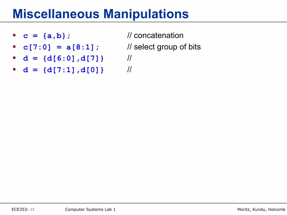
Miscellaneous Manipulations § c = {a,b}; // concatenation § c[7:0] = a[8:1]; // select group of bits § d = {d[6:0],d[7]} // § d = {d[7:1],d[0]} //
ECE353: 14 Computer Systems Lab 1 Moritz, Kundu, Holcomb
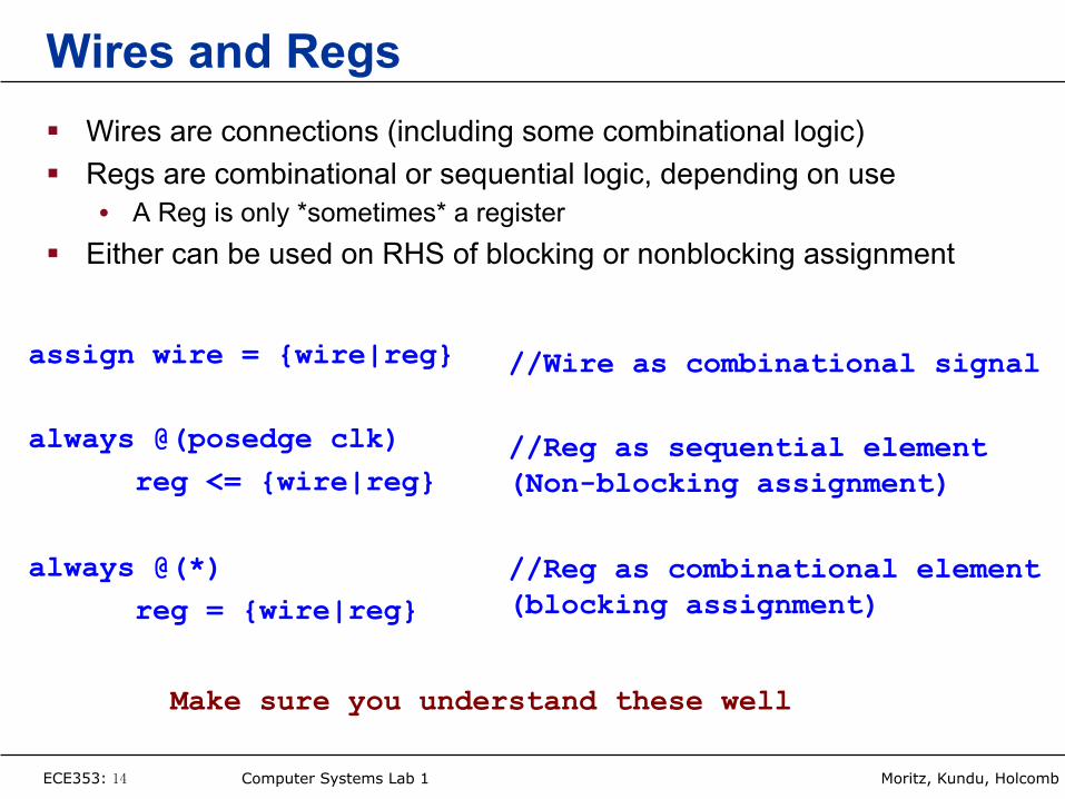
Wires and Regs § Wires are connections (including some combinational logic) § Regs are combinational or sequential logic, depending on use
• A Reg is only *sometimes* a register § Either can be used on RHS of blocking or nonblocking assignment
assign wire = {wire|reg} always @(posedge clk)
reg <= {wire|reg} always @(*)
reg = {wire|reg}
//Wire as combinational signal //Reg as sequential element (Non-blocking assignment) //Reg as combinational element (blocking assignment)
Make sure you understand these well
ECE353: 15 Computer Systems Lab 1 Moritz, Kundu, Holcomb
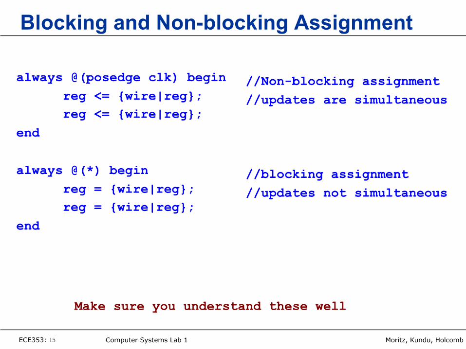
Blocking and Non-blocking Assignment
always @(posedge clk) begin reg <= {wire|reg};
reg <= {wire|reg}; end always @(*) begin
reg = {wire|reg}; reg = {wire|reg};
end
//Non-blocking assignment //updates are simultaneous //blocking assignment //updates not simultaneous
Make sure you understand these well
ECE353: 16 Computer Systems Lab 1 Moritz, Kundu, Holcomb
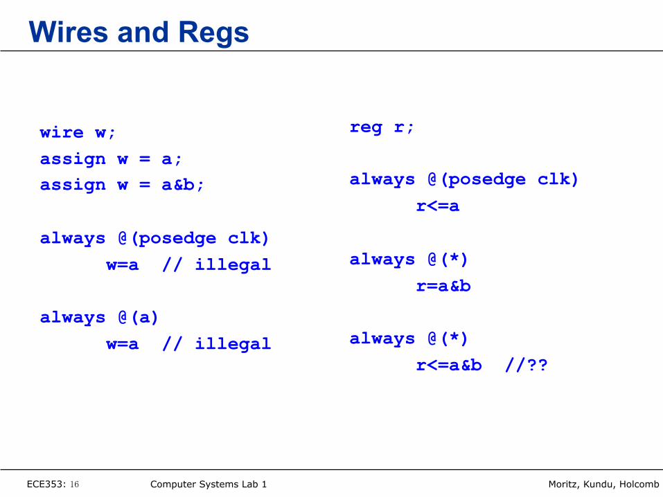
Wires and Regs
wire w; assign w = a; assign w = a&b; always @(posedge clk)
w=a // illegal always @(a)
w=a // illegal
reg r; always @(posedge clk)
r<=a always @(*)
r=a&b always @(*)
r<=a&b //??
ECE353: 17 Computer Systems Lab 1 Moritz, Kundu, Holcomb
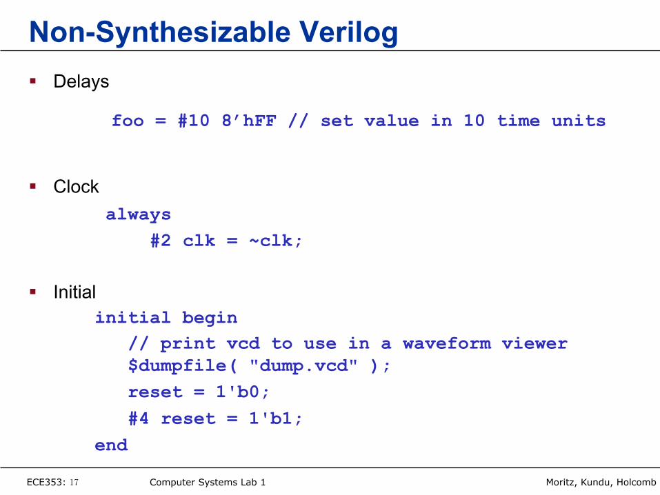
Non-Synthesizable Verilog § Delays
§ Clock
§ Initial
foo = #10 8’hFF // set value in 10 time units
always #2 clk = ~clk;
initial begin // print vcd to use in a waveform viewer
$dumpfile( "dump.vcd" ); reset = 1'b0;
#4 reset = 1'b1; end
ECE353: 18 Computer Systems Lab 1 Moritz, Kundu, Holcomb
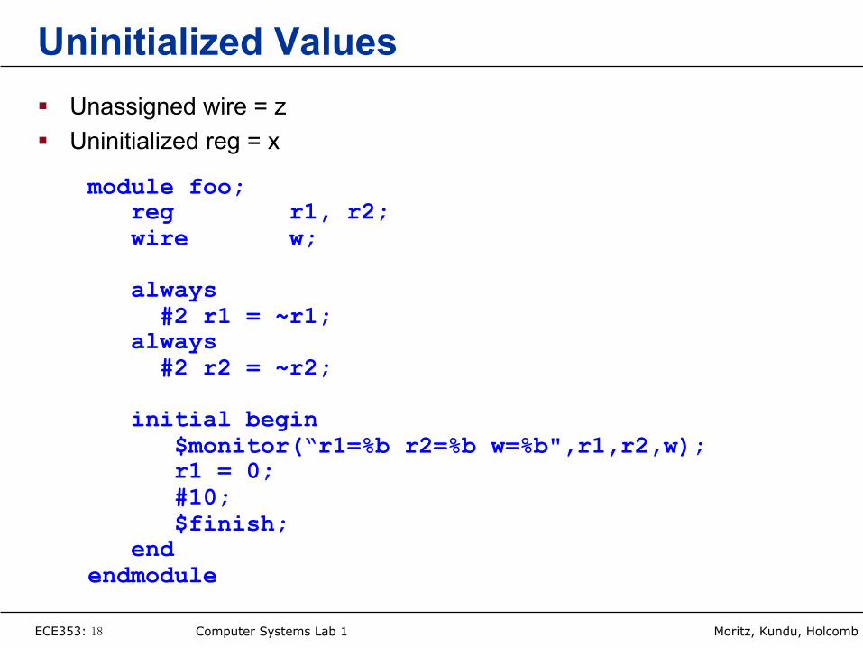
Uninitialized Values § Unassigned wire = z § Uninitialized reg = x
module foo; reg r1, r2; wire w; always #2 r1 = ~r1; always #2 r2 = ~r2; initial begin $monitor(“r1=%b r2=%b w=%b",r1,r2,w); r1 = 0; #10; $finish; end endmodule
ECE353: 19 Computer Systems Lab 1 Moritz, Kundu, Holcomb
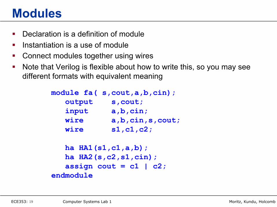
Modules § Declaration is a definition of module § Instantiation is a use of module § Connect modules together using wires § Note that Verilog is flexible about how to write this, so you may see
different formats with equivalent meaning
module fa( s,cout,a,b,cin); output s,cout; input a,b,cin; wire a,b,cin,s,cout; wire s1,c1,c2; ha HA1(s1,c1,a,b); ha HA2(s,c2,s1,cin); assign cout = c1 | c2; endmodule
ECE353: 20 Computer Systems Lab 1 Moritz, Kundu, Holcomb
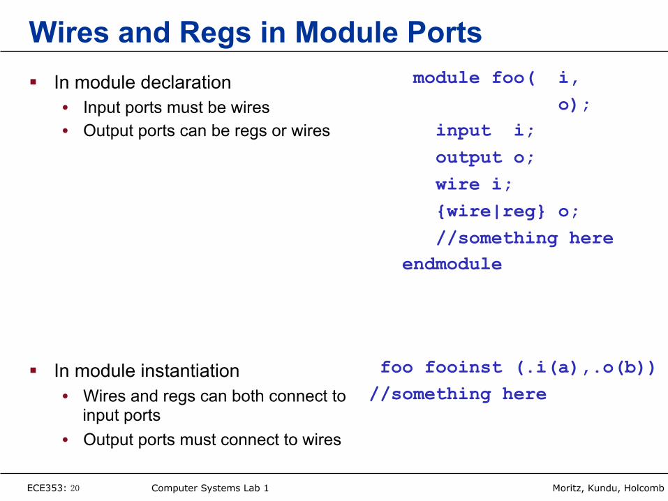
Wires and Regs in Module Ports § In module declaration
• Input ports must be wires • Output ports can be regs or wires
§ In module instantiation • Wires and regs can both connect to
input ports • Output ports must connect to wires
module foo( i, o);
input i; output o; wire i; {wire|reg} o; //something here endmodule
foo fooinst (.i(a),.o(b)) //something here
ECE353: 21 Computer Systems Lab 1 Moritz, Kundu, Holcomb
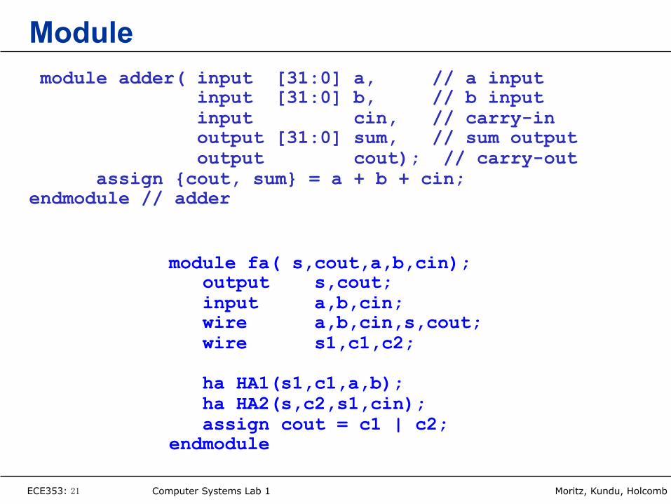
Module module adder( input [31:0] a, // a input input [31:0] b, // b input input cin, // carry-in output [31:0] sum, // sum output output cout); // carry-out
assign {cout, sum} = a + b + cin; endmodule // adder
module fa( s,cout,a,b,cin); output s,cout; input a,b,cin; wire a,b,cin,s,cout; wire s1,c1,c2; ha HA1(s1,c1,a,b); ha HA2(s,c2,s1,cin); assign cout = c1 | c2; endmodule
ECE353: 22 Computer Systems Lab 1 Moritz, Kundu, Holcomb
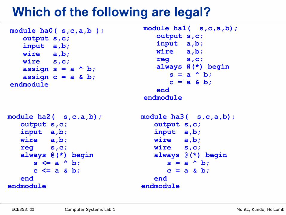
Which of the following are legal? module ha0( s,c,a,b ); output s,c; input a,b; wire a,b; wire s,c; assign s = a ^ b; assign c = a & b; endmodule
module ha3( s,c,a,b); output s,c; input a,b; wire a,b; wire s,c; always @(*) begin s = a ^ b; c = a & b; end endmodule
module ha1( s,c,a,b); output s,c; input a,b; wire a,b; reg s,c; always @(*) begin s = a ^ b; c = a & b; end endmodule
module ha2( s,c,a,b); output s,c; input a,b; wire a,b; reg s,c; always @(*) begin s <= a ^ b; c <= a & b; end endmodule
ECE353: 23 Computer Systems Lab 1 Moritz, Kundu, Holcomb
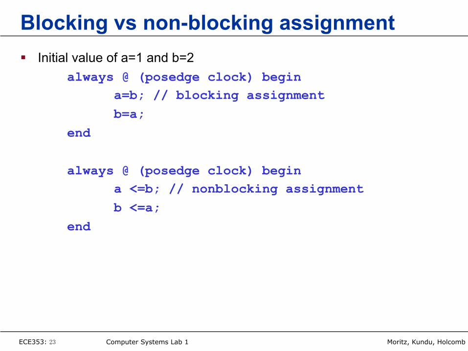
Blocking vs non-blocking assignment § Initial value of a=1 and b=2
always @ (posedge clock) begin a=b; // blocking assignment b=a; end
always @ (posedge clock) begin a <=b; // nonblocking assignment b <=a; end
ECE353: 24 Computer Systems Lab 1 Moritz, Kundu, Holcomb
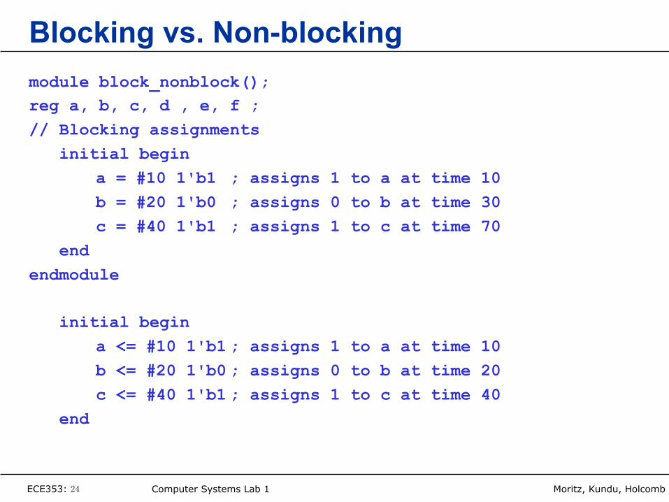
Blocking vs. Non-blocking module block_nonblock(); reg a, b, c, d , e, f ; // Blocking assignments initial begin
a = #10 1'b1 ; assigns 1 to a at time 10 b = #20 1'b0 ; assigns 0 to b at time 30 c = #40 1'b1 ; assigns 1 to c at time 70
end endmodule initial begin
a <= #10 1'b1 ; assigns 1 to a at time 10 b <= #20 1'b0 ; assigns 0 to b at time 20 c <= #40 1'b1 ; assigns 1 to c at time 40
end
ECE353: 25 Computer Systems Lab 1 Moritz, Kundu, Holcomb
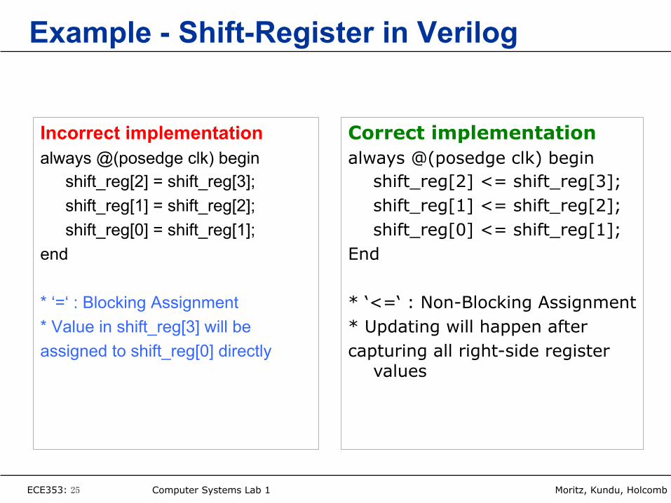
Example - Shift-Register in Verilog
Incorrect implementation always @(posedge clk) begin
shift_reg[2] = shift_reg[3]; shift_reg[1] = shift_reg[2]; shift_reg[0] = shift_reg[1];
end * ‘=‘ : Blocking Assignment * Value in shift_reg[3] will be assigned to shift_reg[0] directly
Correct implementation always @(posedge clk) begin
shift_reg[2] <= shift_reg[3]; shift_reg[1] <= shift_reg[2]; shift_reg[0] <= shift_reg[1];
End * ‘<=‘ : Non-Blocking Assignment * Updating will happen after capturing all right-side register
values
ECE353: 26 Computer Systems Lab 1 Moritz, Kundu, Holcomb
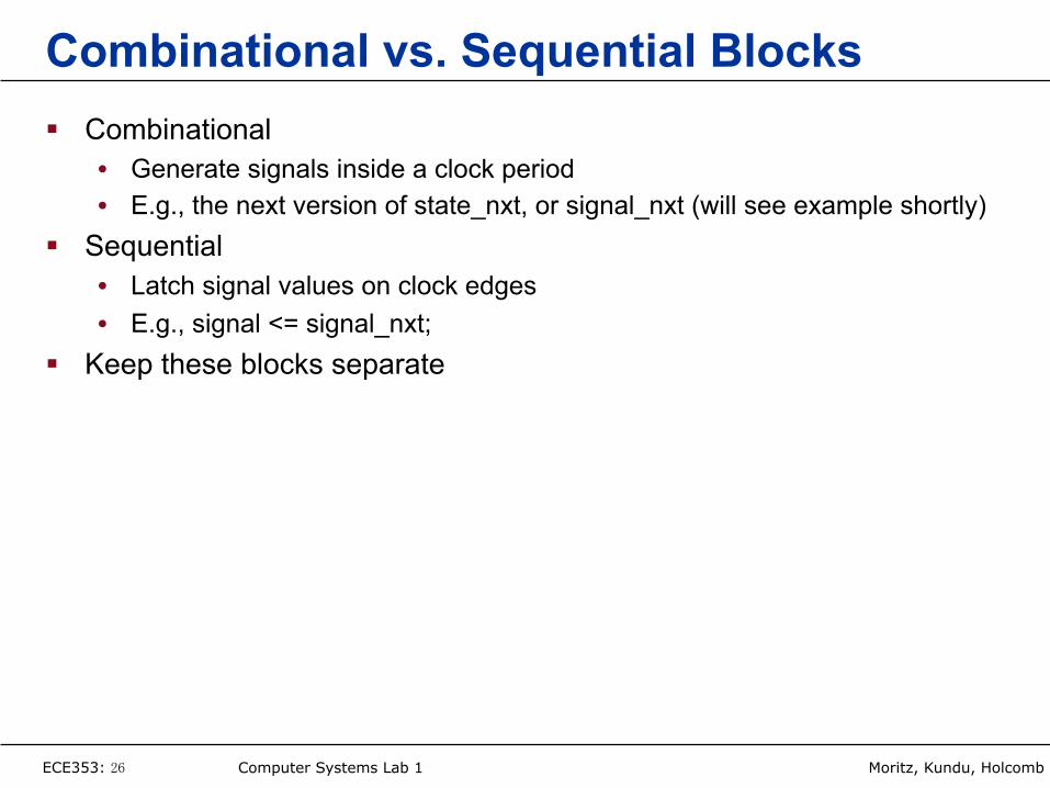
Combinational vs. Sequential Blocks § Combinational
• Generate signals inside a clock period • E.g., the next version of state_nxt, or signal_nxt (will see example shortly)
§ Sequential • Latch signal values on clock edges • E.g., signal <= signal_nxt;
§ Keep these blocks separate
ECE353: 27 Computer Systems Lab 1 Moritz, Kundu, Holcomb
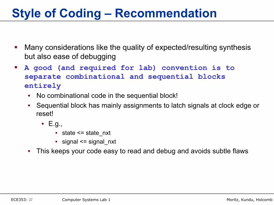
Style of Coding – Recommendation
§ Many considerations like the quality of expected/resulting synthesis but also ease of debugging
§ A good (and required for lab) convention is to separate combinational and sequential blocks entirely • No combinational code in the sequential block! • Sequential block has mainly assignments to latch signals at clock edge or
reset! • E.g.,
• state <= state_nxt • signal <= signal_nxt
• This keeps your code easy to read and debug and avoids subtle flaws
ECE353: 28 Computer Systems Lab 1 Moritz, Kundu, Holcomb
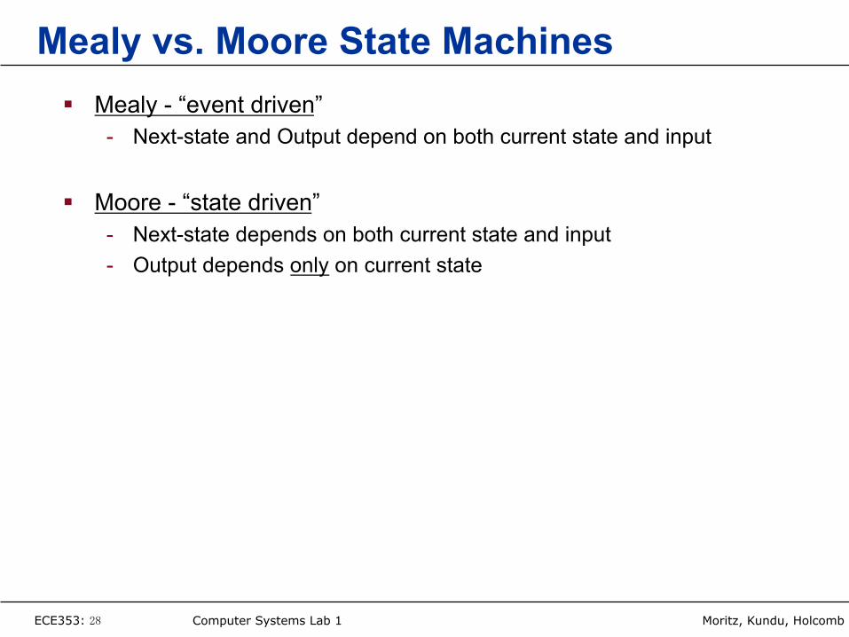
Mealy vs. Moore State Machines § Mealy - “event driven”
- Next-state and Output depend on both current state and input
§ Moore - “state driven” - Next-state depends on both current state and input - Output depends only on current state
ECE353: 29 Computer Systems Lab 1 Moritz, Kundu, Holcomb
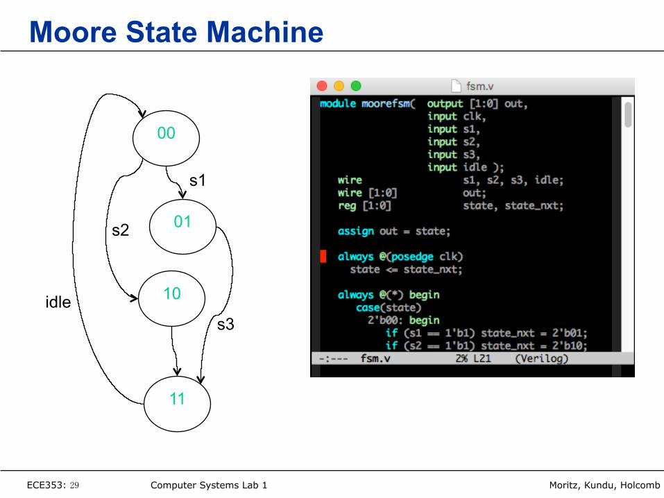
Moore State Machine
00
01
10
11
s1
s2
s3 idle
ECE353: 30 Computer Systems Lab 1 Moritz, Kundu, Holcomb
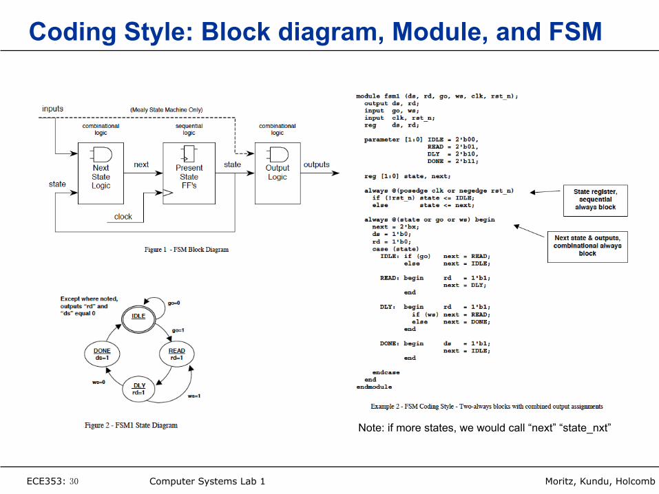
Coding Style: Block diagram, Module, and FSM
Note: if more states, we would call “next” “state_nxt”
ECE353: 31 Computer Systems Lab 1 Moritz, Kundu, Holcomb
Hardware Design – Outline § How to Approach the Design Phase § Implementation with Verilog § Requirements for Functional Simulation § Summary
ECE353: 32 Computer Systems Lab 1 Moritz, Kundu, Holcomb
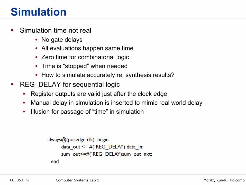
Simulation § Simulation time not real
• No gate delays • All evaluations happen same time • Zero time for combinatorial logic • Time is “stopped” when needed • How to simulate accurately re: synthesis results?
§ REG_DELAY for sequential logic • Register outputs are valid just after the clock edge • Manual delay in simulation is inserted to mimic real world delay • Illusion for passage of “time” in simulation
ECE353: 33 Computer Systems Lab 1 Moritz, Kundu, Holcomb
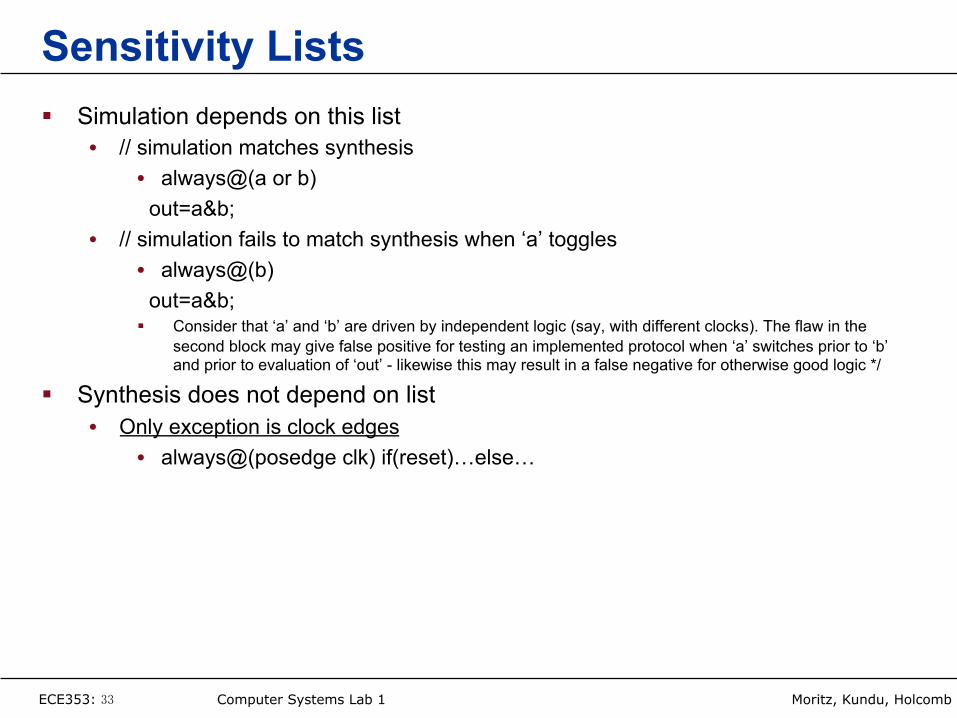
Sensitivity Lists § Simulation depends on this list
• // simulation matches synthesis • always@(a or b) out=a&b;
• // simulation fails to match synthesis when ‘a’ toggles • always@(b) out=a&b; § Consider that ‘a’ and ‘b’ are driven by independent logic (say, with different clocks). The flaw in the
second block may give false positive for testing an implemented protocol when ‘a’ switches prior to ‘b’ and prior to evaluation of ‘out’ - likewise this may result in a false negative for otherwise good logic */
§ Synthesis does not depend on list • Only exception is clock edges
• always@(posedge clk) if(reset)…else…
ECE353: 34 Computer Systems Lab 1 Moritz, Kundu, Holcomb
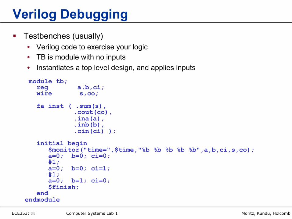
Verilog Debugging § Testbenches (usually)
• Verilog code to exercise your logic • TB is module with no inputs • Instantiates a top level design, and applies inputs
module tb; reg a,b,ci; wire s,co; fa inst ( .sum(s),
.cout(co), .ina(a), .inb(b), .cin(ci) );
initial begin $monitor("time=",$time,"%b %b %b %b %b",a,b,ci,s,co); a=0; b=0; ci=0; #1; a=0; b=0; ci=1; #1; a=0; b=1; ci=0; $finish; end endmodule
ECE353: 35 Computer Systems Lab 1 Moritz, Kundu, Holcomb
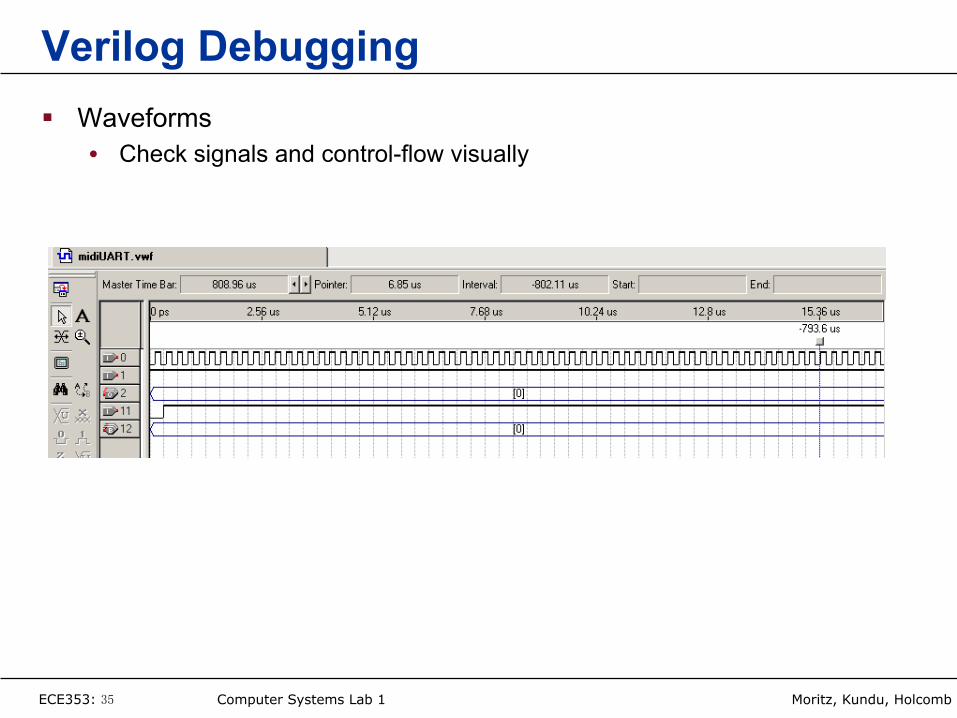
Verilog Debugging § Waveforms
• Check signals and control-flow visually
ECE353: 36 Computer Systems Lab 1 Moritz, Kundu, Holcomb
Hardware Design – Outline § How to Approach the Design Phase § Implementation with Verilog § Requirements for Functional Simulation § Summary
ECE353: 37 Computer Systems Lab 1 Moritz, Kundu, Holcomb
Summary – Coding Style Reviewed
§ Partition into modules if needed § Stub out all inputs and outputs and comment § Separate combinational block(s) from sequential block
• FSM is implemented in combinational block • Next state is calculated in combinational block • Output is calculated in combinational block
• Sequential block mainly contains simple latching assignments § Make sure you use NB statements in sequential and B in
combinational blocks § Use intuitive names (signal, signal_nxt) and follow convention
• Remember this is hardware not software
ECE353: 38 Computer Systems Lab 1 Moritz, Kundu, Holcomb
Additional Information § Please consult course website § Also check lab deliverables in lab assignment document