Embed Size (px)
Citation preview
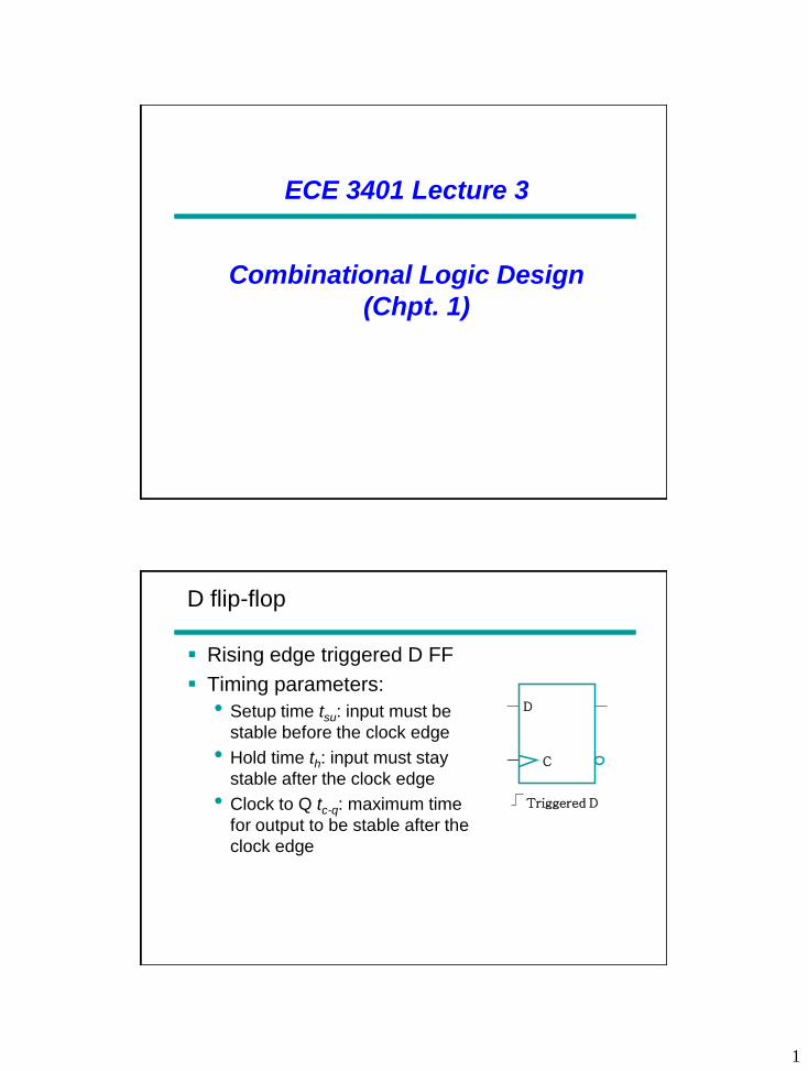
1
ECE 3401 Lecture 3
Combinational Logic Design
(Chpt. 1)
D flip-flop
Rising edge triggered D FF
Timing parameters:
• Setup time tsu: input must be
stable before the clock edge
• Hold time th: input must stay
stable after the clock edge
• Clock to Q tc-q: maximum time
for output to be stable after the
clock edge
Triggered D
D
C
2
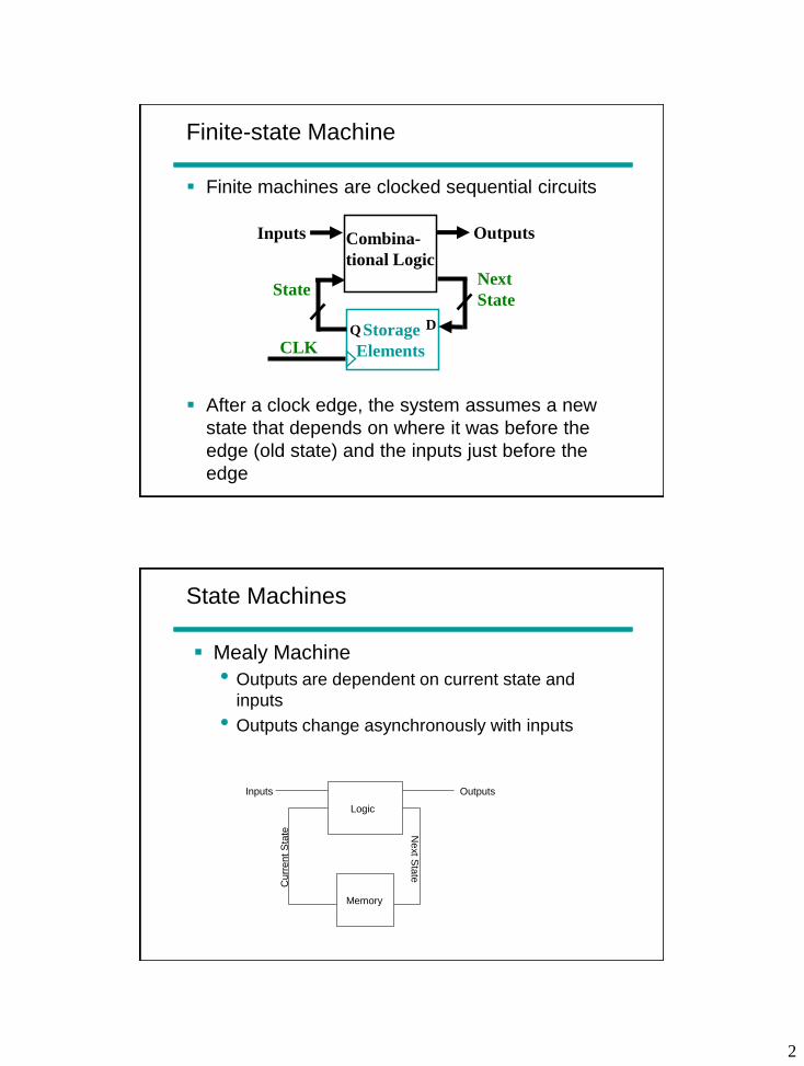
Finite-state Machine
Finite machines are clocked sequential circuits
After a clock edge, the system assumes a new
state that depends on where it was before the
edge (old state) and the inputs just before the
edge
Combina-
tional Logic
Inputs Outputs
State
Next
State
Storage
Elements
D Q
CLK
State Machines
Mealy Machine
• Outputs are dependent on current state and
inputs
• Outputs change asynchronously with inputs
Logic
Memory
Curr
ent
Sta
te
Next S
tate
Inputs Outputs
3
State Machines
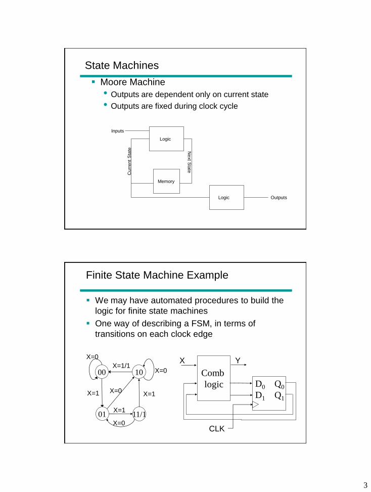
Moore Machine
• Outputs are dependent only on current state
• Outputs are fixed during clock cycle
Logic
Memory
Logic
Curr
ent
Sta
te
Next S
tate
Inputs
Outputs
Finite State Machine Example
We may have automated procedures to build the
logic for finite state machines
One way of describing a FSM, in terms of
transitions on each clock edge
00 10
01 11/1
X=0
X=1
X=1/1 X=0
X=0 X=1
X=1
X=0
Comb
logic
D0 Q0
D1 Q1
X Y
CLK
4
State Machine Design
Make sure
• all states are represented
• all possible inputs are taken into account for state
transitions
• there is an exit out of each state
• there are no conflicts in state transitions
Encodings:
• Binary
• One-Hot
• One-Hot safe
Overview
Logic Design and Implementation Technology
• Design Concepts and Automation
• Design Space: parameters and tradeoffs
• Design Procedure
Major design steps: specification, formulation,
optimization, technology mapping, and verification
5
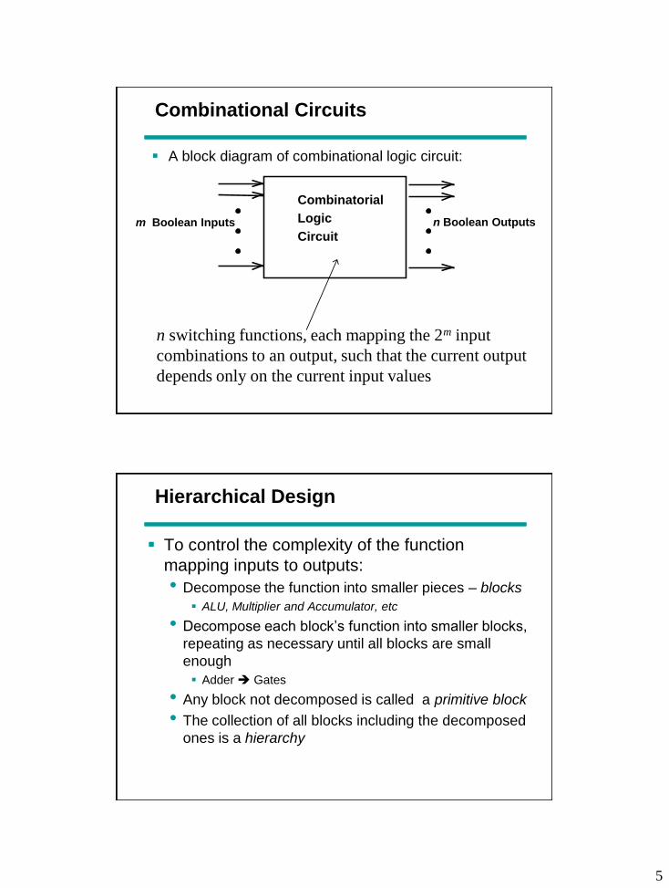
Combinational Circuits
A block diagram of combinational logic circuit:
n switching functions, each mapping the 2m input
combinations to an output, such that the current output
depends only on the current input values
m Boolean Inputs n Boolean Outputs
Combinatorial
Logic
Circuit
Hierarchical Design
To control the complexity of the function
mapping inputs to outputs:
• Decompose the function into smaller pieces – blocks
ALU, Multiplier and Accumulator, etc
• Decompose each block’s function into smaller blocks,
repeating as necessary until all blocks are small
enough
Adder Gates
• Any block not decomposed is called a primitive block
• The collection of all blocks including the decomposed
ones is a hierarchy
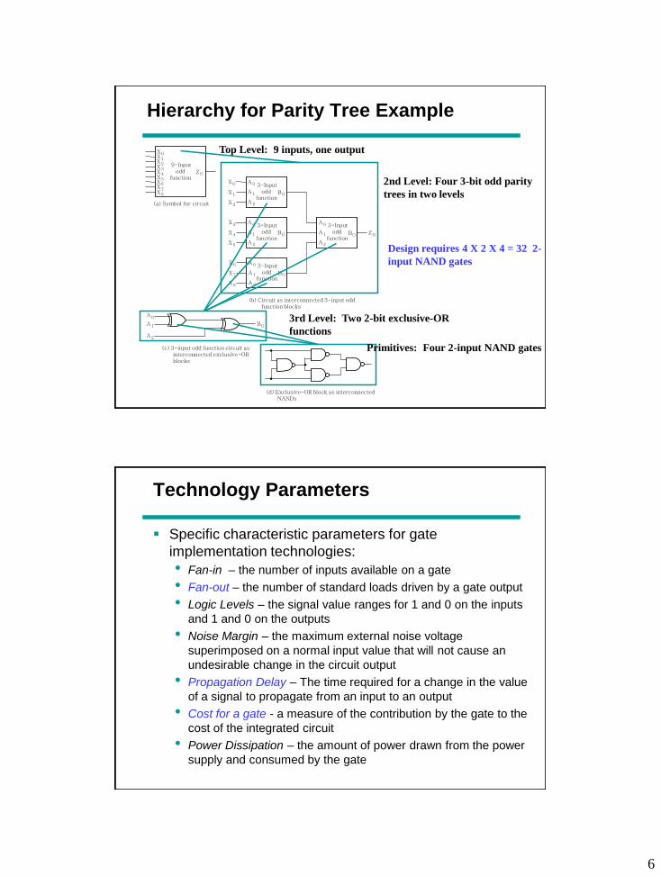
6
Hierarchy for Parity Tree Example
B O
X 0 X 1 X 2 X 3 X 4 X 5 X 6 X 7 X 8
Z O
9-Input odd
function
(a) Symbol for circuit
3-Input
odd
function
A 0
A 1
A 2
B O
3-Input
odd
function
A 0
A 1
A 2
B O
3-Input odd
function
A 0
A 1
A 2
B O
3-Input
odd
function
A 0
A 1
A 2
X 0
X 1
X 2
X 3
X 4
X 5
X 6
X 7
X 8
Z O
(b) Circuit as interconnected 3-input odd
function blocks
B O
A 0
A 1
A 2
(c) 3-input odd function circuit as
interconnected exclusive-OR
blocks
(d) Exclusive-OR block as interconnected
NANDs
Design requires 4 X 2 X 4 = 32 2-
input NAND gates
Top Level: 9 inputs, one output
2nd Level: Four 3-bit odd parity
trees in two levels
3rd Level: Two 2-bit exclusive-OR
functions
Primitives: Four 2-input NAND gates
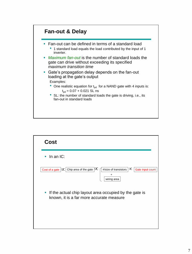
Technology Parameters
Specific characteristic parameters for gate
implementation technologies:
• Fan-in – the number of inputs available on a gate
• Fan-out – the number of standard loads driven by a gate output
• Logic Levels – the signal value ranges for 1 and 0 on the inputs
and 1 and 0 on the outputs
• Noise Margin – the maximum external noise voltage
superimposed on a normal input value that will not cause an
undesirable change in the circuit output
• Propagation Delay – The time required for a change in the value
of a signal to propagate from an input to an output
• Cost for a gate - a measure of the contribution by the gate to the
cost of the integrated circuit
• Power Dissipation – the amount of power drawn from the power
supply and consumed by the gate
7
Fan-out & Delay
Fan-out can be defined in terms of a standard load • 1 standard load equals the load contributed by the input of 1
inverter.
Maximum fan-out is the number of standard loads the gate can drive without exceeding its specified maximum transition time
Gate’s propagation delay depends on the fan-out loading at the gate’s output Examples:
• One realistic equation for tpd for a NAND gate with 4 inputs is:
tpd = 0.07 + 0.021 SL ns
• SL: the number of standard loads the gate is driving, i.e., its fan-out in standard loads
Cost
In an IC:
If the actual chip layout area occupied by the gate is
known, it is a far more accurate measure
Cost of a gate Chip area of the gate #/size of transistors Gate input count
wiring area
+
8
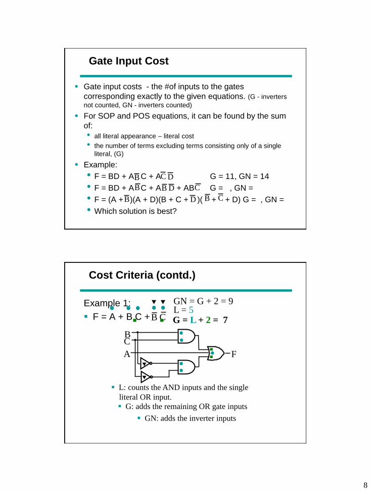
Gate Input Cost
Gate input costs - the #of inputs to the gates
corresponding exactly to the given equations. (G - inverters
not counted, GN - inverters counted)
For SOP and POS equations, it can be found by the sum
of:
• all literal appearance – literal cost
• the number of terms excluding terms consisting only of a single
literal, (G)
Example:
• F = BD + A C + A G = 11, GN = 14
• F = BD + A C + A + AB G = , GN =
• F = (A + )(A + D)(B + C + )( + + D) G = , GN =
• Which solution is best?
D B C B B D C
B D B C
Example 1:
F = A + B C +
Cost Criteria (contd.)
A
B C
F
B C
L = 5
L: counts the AND inputs and the single
literal OR input.
G = L + 2 = 7
G: adds the remaining OR gate inputs
GN = G + 2 = 9
GN: adds the inverter inputs
9
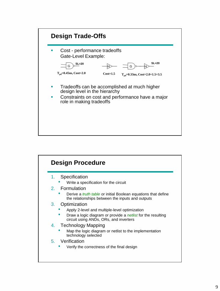
Design Trade-Offs
Cost - performance tradeoffs
Gate-Level Example:
Tradeoffs can be accomplished at much higher design level in the hierarchy
Constraints on cost and performance have a major role in making tradeoffs
G
SL=20
Tpd=0.45ns, Cost=2.0
H
Cost=1.5 Tpd=0.33ns, Cost=2.0+1.5=3.5
G
SL=20
H
Design Procedure
1. Specification • Write a specification for the circuit
2. Formulation • Derive a truth table or initial Boolean equations that define
the relationships between the inputs and outputs
3. Optimization • Apply 2-level and multiple-level optimization
• Draw a logic diagram or provide a netlist for the resulting circuit using ANDs, ORs, and inverters
4. Technology Mapping • Map the logic diagram or netlist to the implementation
technology selected
5. Verification • Verify the correctness of the final design
10
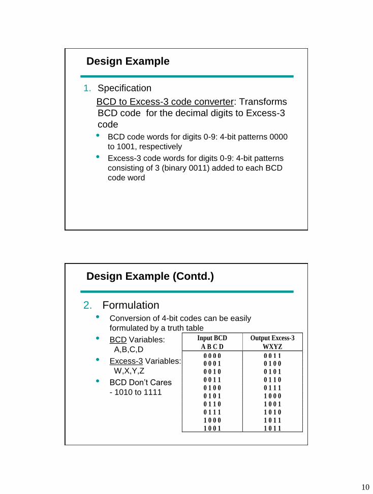
Design Example
1. Specification
BCD to Excess-3 code converter: Transforms
BCD code for the decimal digits to Excess-3
code
• BCD code words for digits 0-9: 4-bit patterns 0000
to 1001, respectively
• Excess-3 code words for digits 0-9: 4-bit patterns
consisting of 3 (binary 0011) added to each BCD
code word
Design Example (Contd.)
2. Formulation • Conversion of 4-bit codes can be easily
formulated by a truth table
• BCD Variables:
A,B,C,D
• Excess-3 Variables:
W,X,Y,Z
• BCD Don’t Cares
- 1010 to 1111
Input BCD
A B C D
Output Excess-3
WXYZ
0 0 0 0 0 0 1 1 0 0 0 1 0 1 0 0 0 0 1 0 0 1 0 1 0 0 1 1 0 1 1 0 0 1 0 0 0 1 1 1 0 1 0 1 1 0 0 0 0 1 1 0 1 0 0 1 0 1 1 1 1 0 1 0 1 0 0 0 1 0 1 1 1 0 0 1 1 0 1 1

11
Design Example (Contd.)
3. Optimization
a. 2-level using
K-maps
B
C
D
A
0 1 3 2
4 5 7 6
12 13 15 14
8 9 11 10
1
1 1
1
X X X
X X
X
1
B
C
D
A
0 1 3 2
4 5 7 6
12 13 15 14
8 9 11 10
1
1 1
1
X X X
X X
X
1
B
C
D
A
0 1 3 2
4 5 7 6
12 13 15 14
8 9 11 10
1 1
1
1
X X X
X X
X
1
B
C
D
A
0 1 3 2
4 5 7 6
12 13 15 14
8 9 11 10
1 1
1
X X X
X X
X
1
1
w
z y
x
B C D B
C D
D
W = A + BC + BD
X = C + D + B
Y = CD +
Z =
Design Example (Contd.)
3. Optimization (Contd.) b. Multiple-level using transformations
W = A + BC + BD X = C + D + B Y = CD + Z = G = 7 + 10 + 6 + 0 = 23
• Perform extraction, finding factor:
T1 = C + D W = A + BT1 X = T1 + B Y = CD + Z = G = 2 + 4 + 7 + 6 + 0 = 19
• An additional extraction using a Boolean transformation: ( = C + D = )
W = A + BT1 X = T1 + B Y = CD + Z = G = 2 + 1 + 4 + 5 + 4 + 0 = 16
B C D B
C D
D
B C D
C D
D
C D
T1
B T1
D T1
12
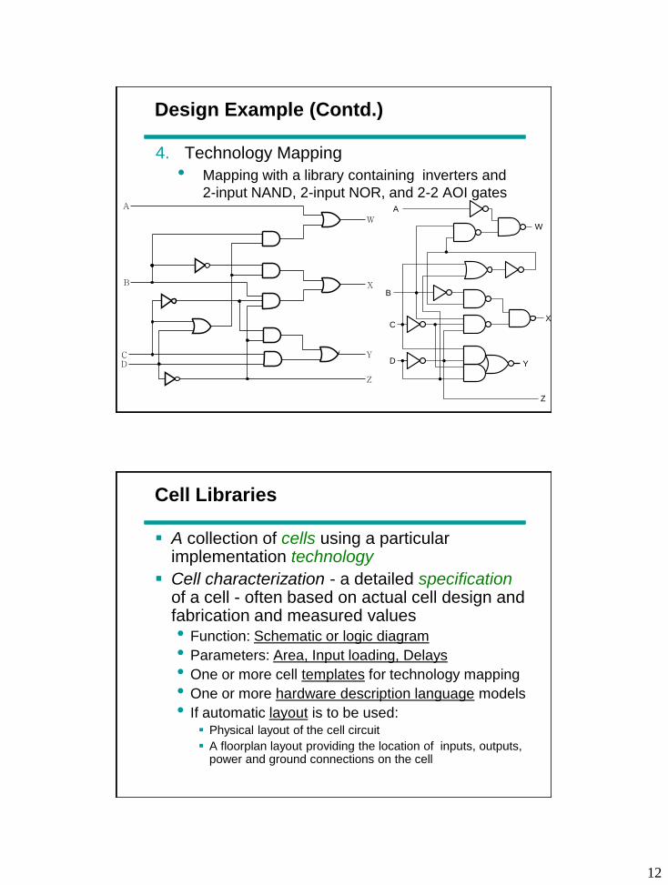
Design Example (Contd.)
4. Technology Mapping
• Mapping with a library containing inverters and
2-input NAND, 2-input NOR, and 2-2 AOI gates A
B
C
D
W
X
Y
Z
A
B
C D
W
X
Y
Z
Cell Libraries
A collection of cells using a particular implementation technology
Cell characterization - a detailed specification of a cell - often based on actual cell design and fabrication and measured values • Function: Schematic or logic diagram
• Parameters: Area, Input loading, Delays
• One or more cell templates for technology mapping
• One or more hardware description language models
• If automatic layout is to be used: Physical layout of the cell circuit
A floorplan layout providing the location of inputs, outputs, power and ground connections on the cell
13
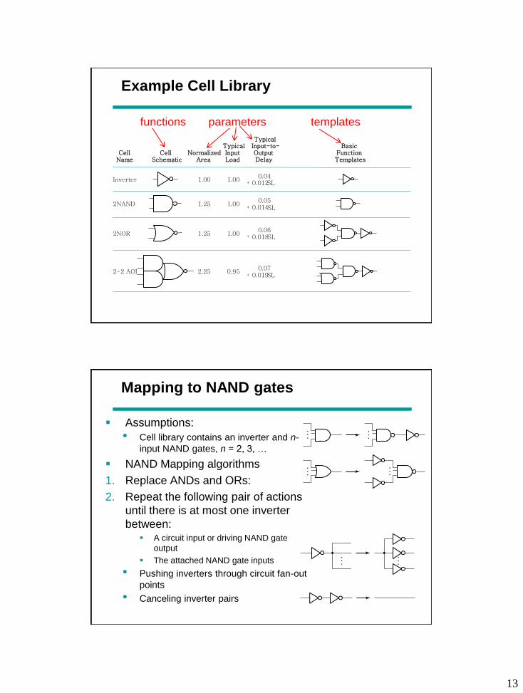
Example Cell Library
Cell Name
Cell Schematic
Normalized Area
Typical Input Load
Typical Input-to- Output Delay
Basic Function Templates
Inverter 1.00 1.00
0.04 + 0.012 SL
2NAND 1.25 1.00 0.05
+ 0.014 SL
2NOR 1.25 1.00 0.06
+ 0.018 SL
2-2 AOI 2.25 0.95 0.07
+ 0.019 SL
functions parameters templates
Mapping to NAND gates
.
.
....
.
.
.
.
.
.
.
.
....
Assumptions:
• Cell library contains an inverter and n-
input NAND gates, n = 2, 3, …
NAND Mapping algorithms
1. Replace ANDs and ORs:
2. Repeat the following pair of actions
until there is at most one inverter
between: A circuit input or driving NAND gate
output
The attached NAND gate inputs
• Pushing inverters through circuit fan-out
points
• Canceling inverter pairs
14
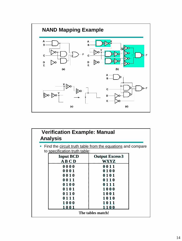
NAND Mapping Example
Input BCD
A B C D
Output Excess - 3
WXYZ
0 0 0 0 0 0 1 1 0 0 0 1 0 1 0 0 0 0 1 0 0 1 0 1 0 0 1 1 0 1 1 0 0 1 0 0 0 1 1 1 0 1 0 1 1 0 0 0 0 1 1 0 1 0 0 1 0 1 1 1 1 0 1 0 1 0 0 0 1 0 1 1 1 0 0 1 1 1 0 0
Verification Example: Manual
Analysis
Find the circuit truth table from the equations and compare
to specification truth table:
The tables match!
Input BCD
A B C D
Output Excess - 3
WXYZ
0 0 0 0 0 0 1 1 0 0 0 1 0 1 0 0 0 0 1 0 0 1 0 1 0 0 1 1 0 1 1 0 0 1 0 0 0 1 1 1 0 1 0 1 1 0 0 0 0 1 1 0 1 0 0 1 0 1 1 1 1 0 1 0 1 0 0 0 1 0 1 1 1 0 0 1 1 1 0 0
15
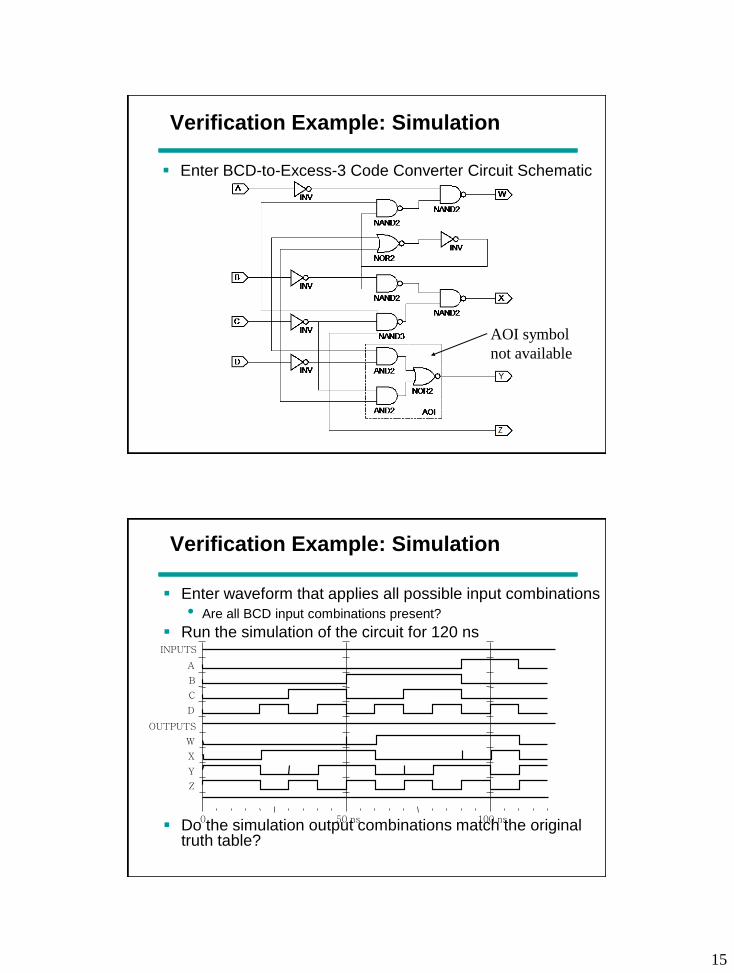
Verification Example: Simulation
Enter BCD-to-Excess-3 Code Converter Circuit Schematic
AOI symbol
not available
Verification Example: Simulation
Enter waveform that applies all possible input combinations
• Are all BCD input combinations present?
Run the simulation of the circuit for 120 ns
Do the simulation output combinations match the original truth table?
INPUTS
A B C D
0 50 ns 100 ns
OUTPUTS
W X Y
Z
16
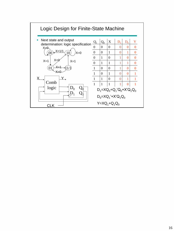
Logic Design for Finite-State Machine
Next state and output
determination: logic specification
00 10
01 11/1
X=0
X=1
X=1/1 X=0
X=0 X=1
X=1
X=0
Q1 Q0 X D1 D0 Y
0 0 0 0 0 0
0 0 1 0 1 0
0 1 0 1 0 0
0 1 1 1 1 0
1 0 0 1 0 0
1 0 1 0 0 1
1 1 0 0 1 1
1 1 1 1 0 1
D1=XQ0+Q1’Q0+X’Q1Q0
D0=XQ1’+X’Q1Q0
Y=XQ1+Q1Q0
Comb
logic
D0 Q0
D1 Q1
X Y
CLK