Embed Size (px)
Citation preview
1
1
ECE 261: CMOS VLSI Design Methodologies
Prof. Krishnendu (Krish) Chakrabarty
Dept. Electrical and Computer Engineering
Room 2513 CIEMAS
Ph: 660-5244
E-mail: [email protected]
URL: http://www.ee.duke.edu/~krish
Course URL:
http://www.ee.duke.edu/~krish/teaching/261.html
2
Course Objectives
• Introduction to CMOS VLSI design methodologies– Emphasis on full-custom design
– Circuit and system levels
• Extensive use of Mentor Graphics CAD tools for IC design, simulation, and layout verification
• Specific techniques for designing high-speed, low-power, and easily-testable circuits
2
4
Introduction• Integrated circuits: many transistors on one chip.
• Very Large Scale Integration (VLSI): bucketloads!
• Complementary Metal Oxide Semiconductor – Fast, cheap, low power transistors
• Today: How to build your own simple CMOS chip– CMOS transistors
– Building logic gates from transistors
– Transistor layout and fabrication
• Rest of the course: How to build a good CMOS chip
3
5
Designing for VLSI
• Designing a system on a chip– Craft components from silicon rather than selecting catalog parts
• ICs (chips) are batch fabricated– Inexpensive unit cost
• Bugs are hard to fix!– Extensive design verification needed
6
VLSI Design: Overview• VLSI design is system design
– Designing fast inverters is fun, but need knowledge of all aspects of digital design: algorithms, systems, circuits, fabrication, and packaging
– Need to bridge gap between abstract vision of digital design and the underlying digital circuit and its peculiarities
– Circuit-level optimization, verification, and testing techniques are important
• Tall thin approach does not always work– Today’s designer is “fatter”, but well-versed in both high-level and
low-level design skills
4
7
VLSI: Enabling Technology• Automotive electronic systems
– A typical car has over 100 ICs (stereo systems, display panels, fuel injection systems, smart suspensions, antilock brakes, airbags)
• Signal Processing (DSP chips, data acquisition systems)
• Transaction processing (bank ATMs)
• PCs, workstations, servers, consumer electronics
• Medical electronics (artificial eye, implants)
• Avionics, space applications
• Networking hardware: Routers and switches
• …..
The Semiconductor Industry
• 53% compound annual growth rate over 50 years– No other technology has grown so fast so long
• Driven by miniaturization of transistors– Smaller is cheaper, faster, lower in power!
– Revolutionary effects on society
8

5
9
Design Complexity
• Transistor counts and IC densities continue to grow!– Moore’s Law-The number of transistors on an IC doubles every
1.5 years
– Intel x486: 1 million transistors (1989), PowerPC: 2-3 million transistors (1994), Pentium: 3.1 million transistors (1994), DEC Alpha: 10 million transistors (1995)-9 million in SRAM, Pentium IV (2001): 42 million transistors
• Memory (DRAM) is the “technology driver”– 256 Mbits DRAM now commercially available
10
VLSI Technology
• CMOS: Complementary Metal Oxide Silicon– Based on voltage-controlled field-effect transistors (FETs)
• Other technologies: bipolar junction transistors (BJTs), BiCMOS, gallium arsenide (GaAs)– BJTs, BiCMOS, ECL circuits are faster but CMOS consumes
lower power and are easier to fabricate
– GaAs carriers have higher mobility but high integration levels are difficult to achieve in GaAs technology
6
11
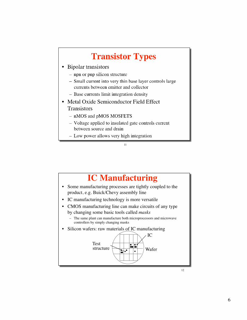
Transistor Types• Bipolar transistors
– npn or pnp silicon structure
– Small current into very thin base layer controls large currents between emitter and collector
– Base currents limit integration density
• Metal Oxide Semiconductor Field Effect Transistors– nMOS and pMOS MOSFETS
– Voltage applied to insulated gate controls current between source and drain
– Low power allows very high integration
12
IC Manufacturing• Some manufacturing processes are tightly coupled to the
product, e.g. Buick/Chevy assembly line
• IC manufacturing technology is more versatile
• CMOS manufacturing line can make circuits of any type by changing some basic tools called masks– The same plant can manufacture both microprocessors and microwave
controllers by simply changing masks
• Silicon wafers: raw materials of IC manufacturing
Teststructure Wafer
IC

7
13
Silicon Lattice• Transistors are built on a silicon substrate
• Silicon is a Group IV material
• Forms crystal lattice with bonds to four neighbors
14
Chip Designer’s Lexicon
• Boston geometry: masks that use only curves– In contrast to Manhattan and Euclidean geometries
• Dog and pony show: A presentation to management
• Hit by a truck: Losing a key technical person at a crucial point in a project (especially common in the IC design industry today!)
• Infant mortality: failure of ICs during the first few hours of operation
8
15
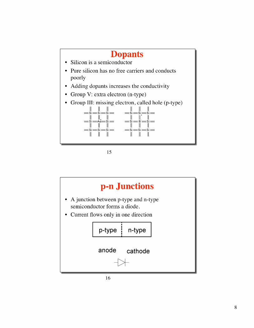
Dopants• Silicon is a semiconductor
• Pure silicon has no free carriers and conducts poorly
• Adding dopants increases the conductivity
• Group V: extra electron (n-type)
• Group III: missing electron, called hole (p-type)
16
p-n Junctions• A junction between p-type and n-type
semiconductor forms a diode.
• Current flows only in one direction
9
17
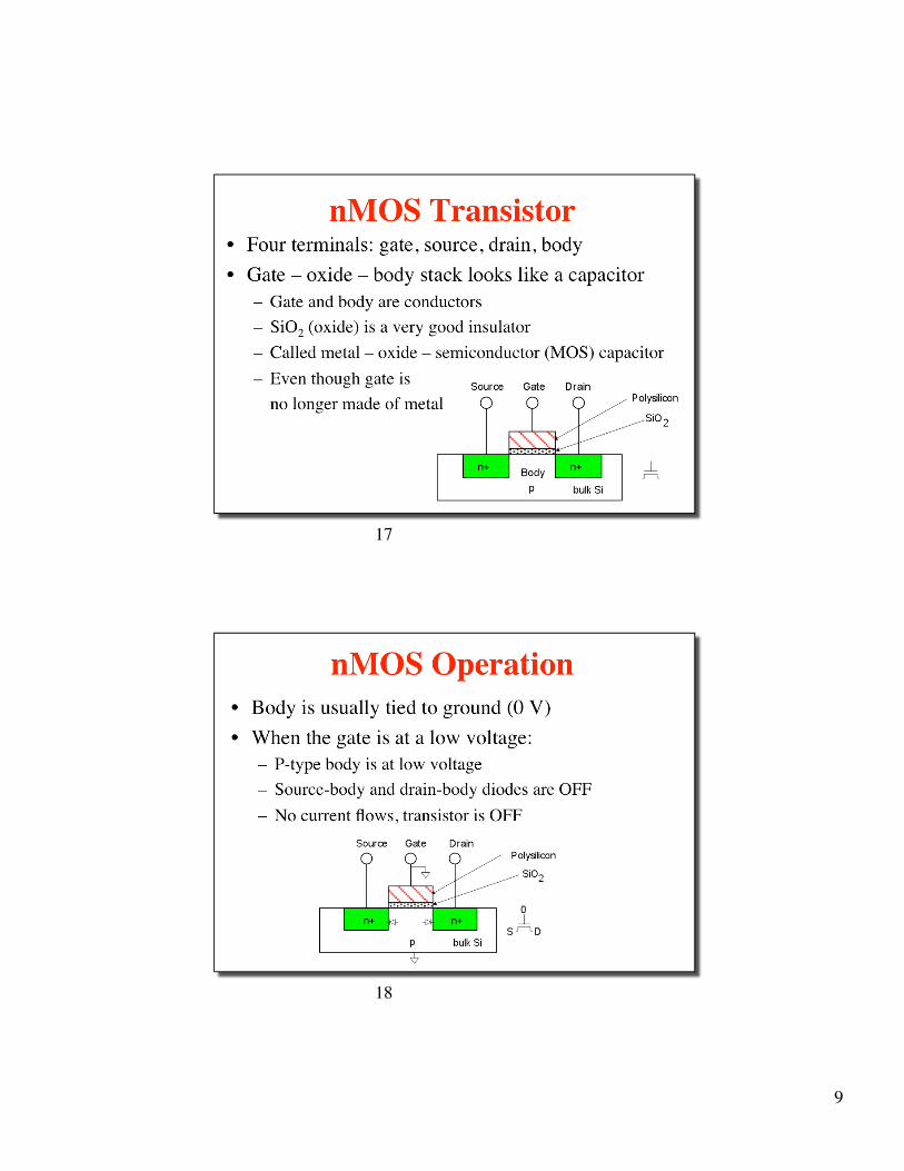
nMOS Transistor• Four terminals: gate, source, drain, body
• Gate – oxide – body stack looks like a capacitor– Gate and body are conductors
– SiO2 (oxide) is a very good insulator
– Called metal – oxide – semiconductor (MOS) capacitor
– Even though gate is
no longer made of metal
18
nMOS Operation• Body is usually tied to ground (0 V)
• When the gate is at a low voltage:– P-type body is at low voltage
– Source-body and drain-body diodes are OFF
– No current flows, transistor is OFF

10
19
nMOS Operation (Contd.)• When the gate is at a high voltage:
– Positive charge on gate of MOS capacitor
– Negative charge attracted to body
– Inverts a channel under gate to n-type
– Now current can flow through n-type silicon from source through channel to drain, transistor is ON
20
pMOS Transistor• Similar, but doping and voltages reversed
– Body tied to high voltage (VDD)
– Gate low: transistor ON
– Gate high: transistor OFF
– Bubble indicates inverted behavior

11
21
Power Supply Voltage
• GND = 0 V
• In 1980’s, VDD = 5V
• VDD has decreased in modern processes– High VDD would damage modern tiny transistors
– Lower VDD saves power
• VDD = 3.3, 2.5, 1.8, 1.5, 1.2, 1.0, …
22
Growth Rate
• 53% compound annual growth rate over 50 years– No other technology has grown so fast so long
• Driven by miniaturization of transistors– Smaller is cheaper, faster, lower in power!
– Revolutionary effects on society

12
23
Annual Sales• >1019 transistors manufactured in 2008
– 1 billion for every human on the planet
24
• 1970’s processes usually had only nMOS transistors– Inexpensive, but consume power while idle
• 1980s-present: CMOS processes for low idle power
MOS Integrated Circuits
Intel 1101 256-bit SRAM Intel 4004 4-bit μProc
[Vadasz69]
© 1969 IEEE.
Intel
Museum.
Reprinted
with
permission.
13
25
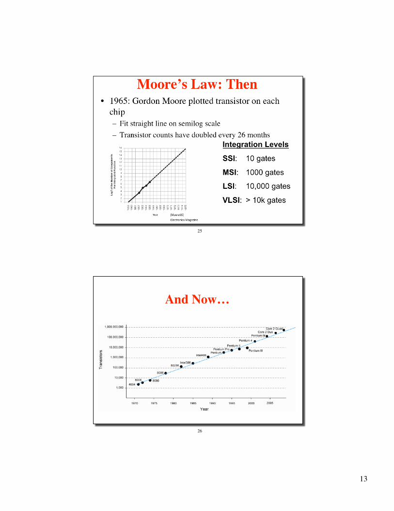
Moore’s Law: Then• 1965: Gordon Moore plotted transistor on each
chip– Fit straight line on semilog scale
– Transistor counts have doubled every 26 monthsIntegration Levels
SSI: 10 gates
MSI: 1000 gates
LSI: 10,000 gates
VLSI: > 10k gates
[Moore65]
Electronics Magazine
26
And Now…

14
27
28
Feature Size
• Minimum feature size shrinking 30% every 2-3 years

15
29
Corollaries• Many other factors grow exponentially
– Ex: clock frequency, processor performance
Cost of Fabs
30
16
31
Some History
• Basic principles of MOS: Lilienfield (1925), Heil (1935)– Problem: Fabrication, materials processing
– BJT transistors were designed at Bell Labs in the late forties and fifties (sixty years of the transistor!)
• MOS planar process: 1960, Weiner (CMOS flip-flops:1962), Wanlass (inverter, NOR, NAND gates: 1963)
32
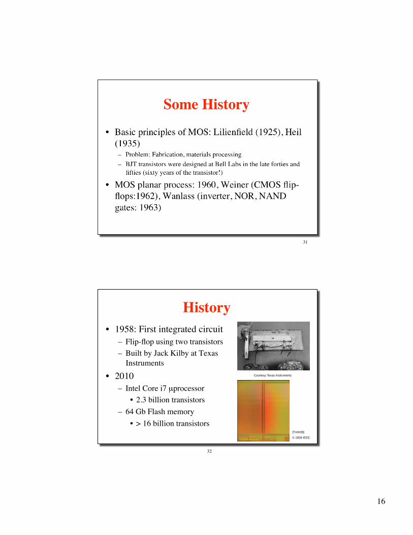
History• 1958: First integrated circuit
– Flip-flop using two transistors
– Built by Jack Kilby at Texas Instruments
• 2010– Intel Core i7 μprocessor
• 2.3 billion transistors
– 64 Gb Flash memory
• > 16 billion transistors
Courtesy Texas Instruments
[Trinh09]
© 2009 IEEE.
17
33
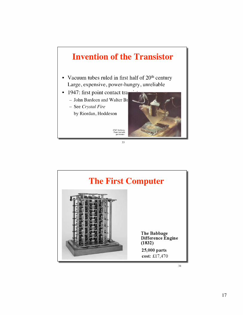
Invention of the Transistor
• Vacuum tubes ruled in first half of 20th century Large, expensive, power-hungry, unreliable
• 1947: first point contact transistor– John Bardeen and Walter Brattain at Bell Labs
– See Crystal Fire
by Riordan, Hoddeson
AT&T Archives.
Reprinted with
permission.
34
The First Computer

18
35
ENIAC - The first electronic computer (1946)
36
Intel 4004 Micro-Processor1971, 2300 transistors, 10 microns process
19
37
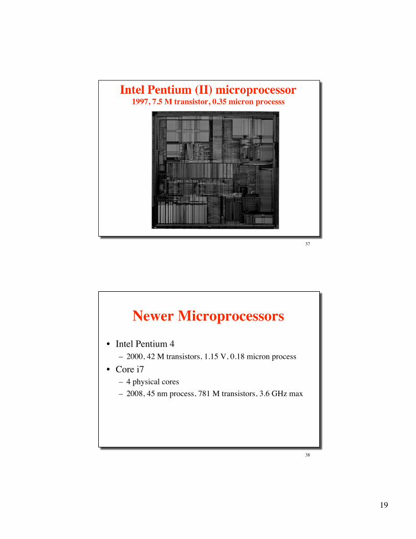
Intel Pentium (II) microprocessor1997, 7.5 M transistor, 0.35 micron processs
Newer Microprocessors
• Intel Pentium 4– 2000, 42 M transistors, 1.15 V, 0.18 micron process
• Core i7– 4 physical cores
– 2008, 45 nm process, 781 M transistors, 3.6 GHz max
38
20
39
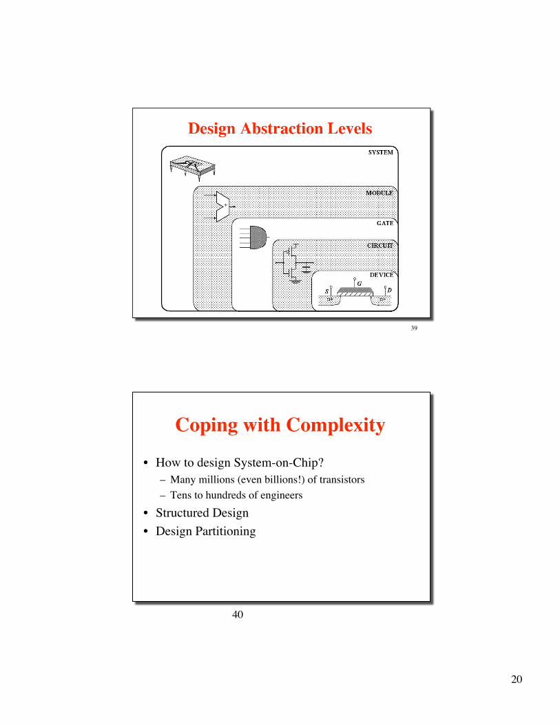
Design Abstraction Levels
40
Coping with Complexity
• How to design System-on-Chip?– Many millions (even billions!) of transistors
– Tens to hundreds of engineers
• Structured Design
• Design Partitioning
21
41
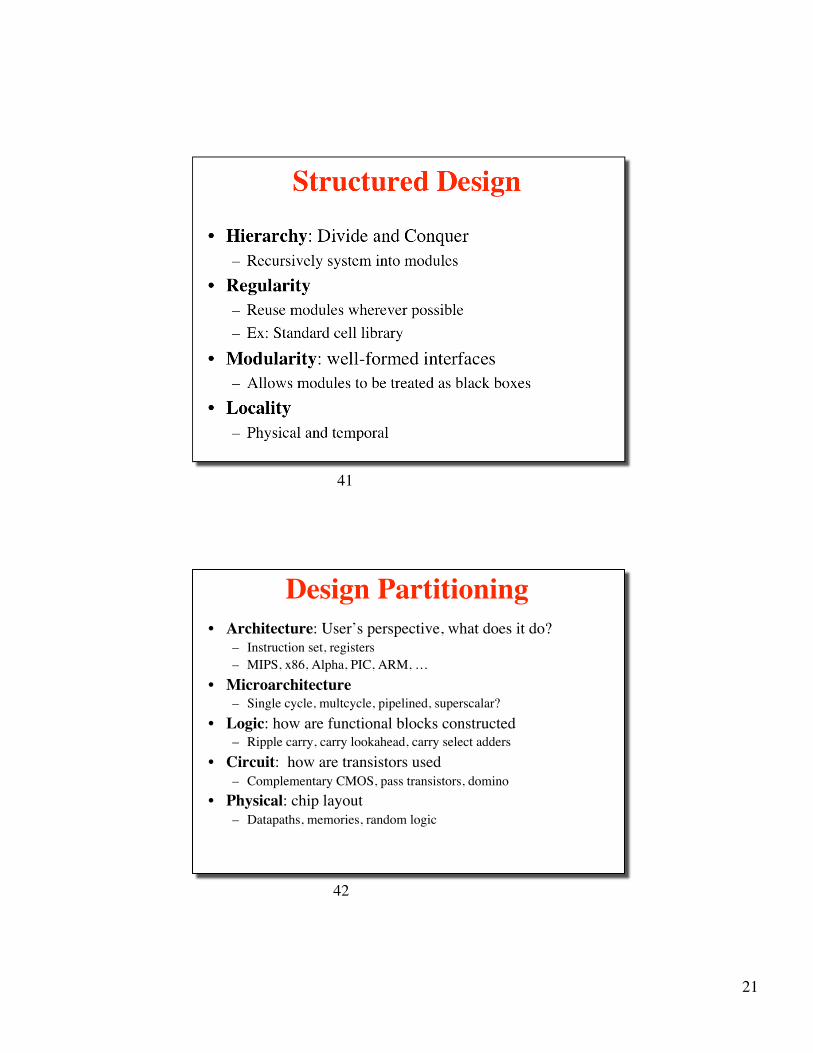
Structured Design
• Hierarchy: Divide and Conquer– Recursively system into modules
• Regularity– Reuse modules wherever possible
– Ex: Standard cell library
• Modularity: well-formed interfaces– Allows modules to be treated as black boxes
• Locality– Physical and temporal
42
Design Partitioning• Architecture: User’s perspective, what does it do?
– Instruction set, registers– MIPS, x86, Alpha, PIC, ARM, …
• Microarchitecture– Single cycle, multcycle, pipelined, superscalar?
• Logic: how are functional blocks constructed– Ripple carry, carry lookahead, carry select adders
• Circuit: how are transistors used– Complementary CMOS, pass transistors, domino
• Physical: chip layout– Datapaths, memories, random logic
22
43
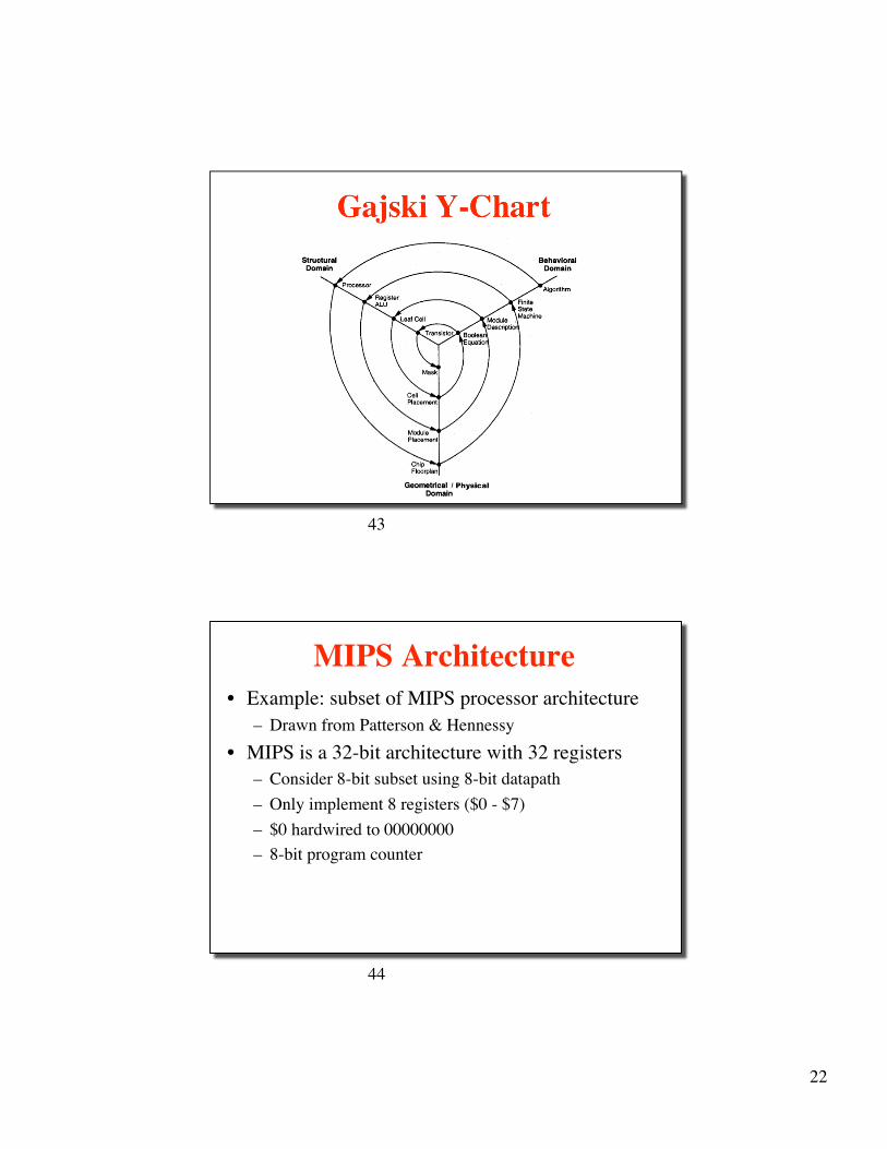
Gajski Y-Chart
44
MIPS Architecture• Example: subset of MIPS processor architecture
– Drawn from Patterson & Hennessy
• MIPS is a 32-bit architecture with 32 registers– Consider 8-bit subset using 8-bit datapath
– Only implement 8 registers ($0 - $7)
– $0 hardwired to 00000000
– 8-bit program counter
23
45
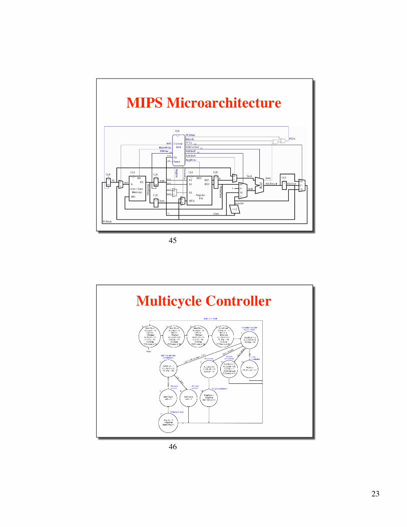
MIPS Microarchitecture
• Multicycle μarchitecture ( [Paterson04], [Harris07] )
46
Multicycle Controller

24
47
Logic Design
• Start at top level– Hierarchically decompose MIPS into units
• Top-level interface
48
Block Diagram
25
49
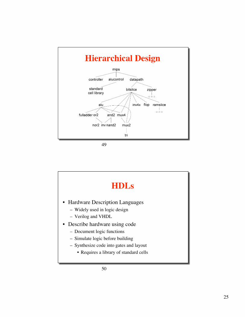
Hierarchical Design
50
HDLs
• Hardware Description Languages– Widely used in logic design
– Verilog and VHDL
• Describe hardware using code– Document logic functions
– Simulate logic before building
– Synthesize code into gates and layout
• Requires a library of standard cells
26
51
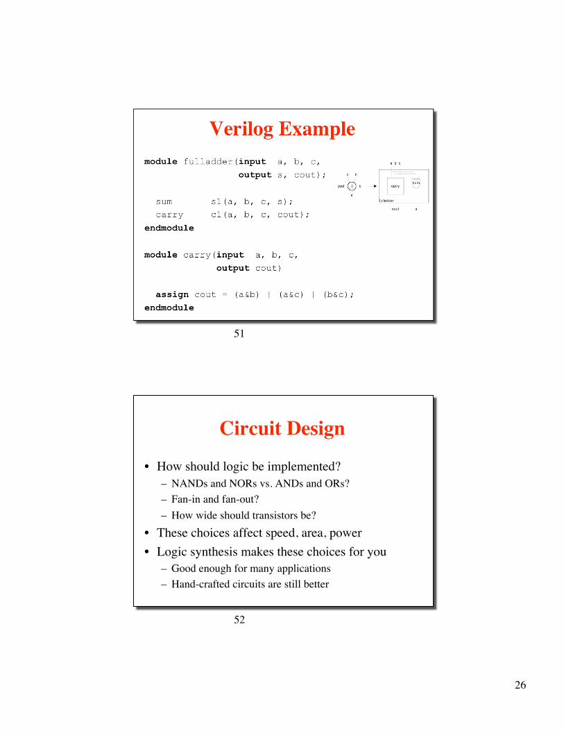
Verilog Examplemodule fulladder(input a, b, c,
output s, cout);
sum s1(a, b, c, s);
carry c1(a, b, c, cout);
endmodule
module carry(input a, b, c,
output cout)
assign cout = (a&b) | (a&c) | (b&c);
endmodule
52
Circuit Design
• How should logic be implemented?– NANDs and NORs vs. ANDs and ORs?
– Fan-in and fan-out?
– How wide should transistors be?
• These choices affect speed, area, power
• Logic synthesis makes these choices for you– Good enough for many applications
– Hand-crafted circuits are still better
27
53
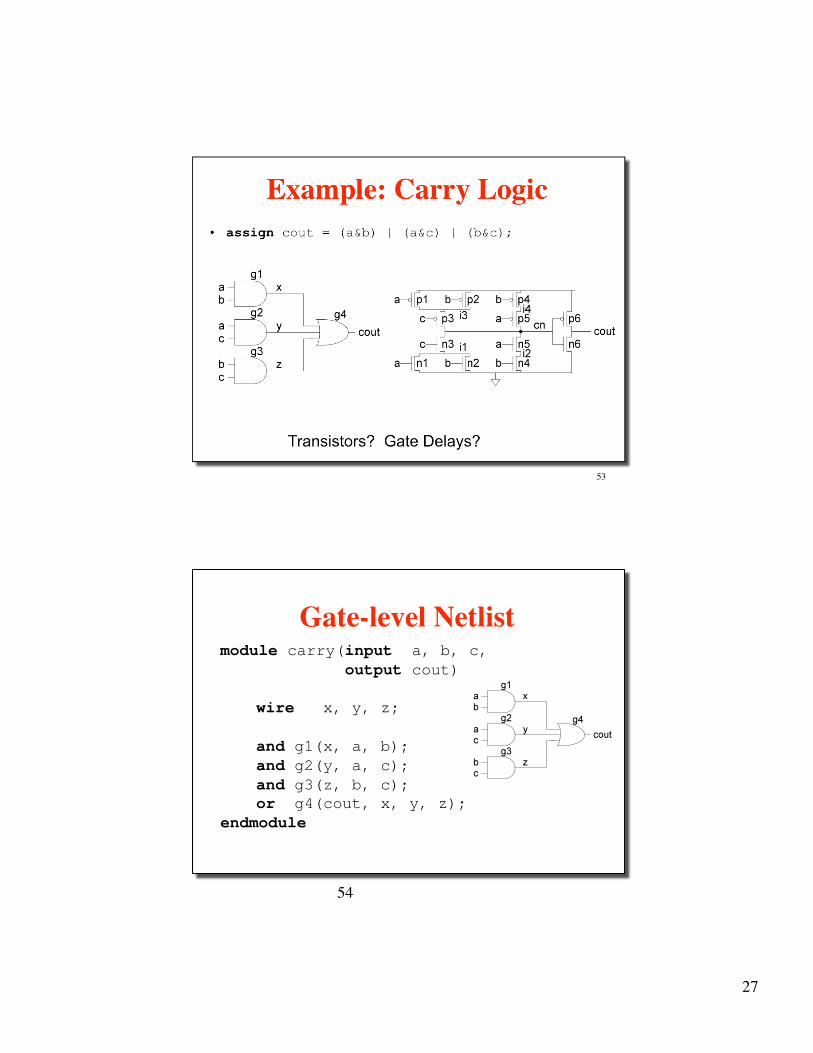
Example: Carry Logic• assign cout = (a&b) | (a&c) | (b&c);
Transistors? Gate Delays?
54
Gate-level Netlistmodule carry(input a, b, c,
output cout)
wire x, y, z;
and g1(x, a, b);
and g2(y, a, c);
and g3(z, b, c);
or g4(cout, x, y, z);
endmodule
28
55
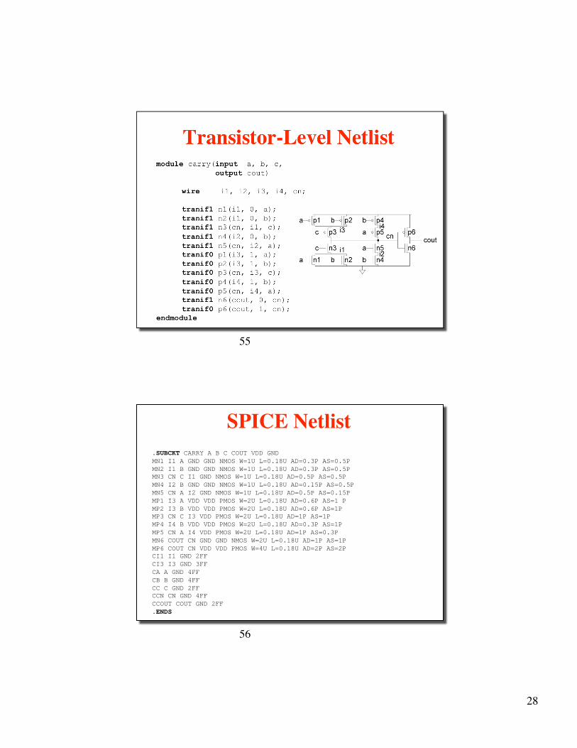
Transistor-Level Netlistmodule carry(input a, b, c,
output cout)
wire i1, i2, i3, i4, cn;
tranif1 n1(i1, 0, a);
tranif1 n2(i1, 0, b);
tranif1 n3(cn, i1, c);
tranif1 n4(i2, 0, b);
tranif1 n5(cn, i2, a);
tranif0 p1(i3, 1, a);
tranif0 p2(i3, 1, b);
tranif0 p3(cn, i3, c);
tranif0 p4(i4, 1, b);
tranif0 p5(cn, i4, a);
tranif1 n6(cout, 0, cn);
tranif0 p6(cout, 1, cn);
endmodule
56
SPICE Netlist.SUBCKT CARRY A B C COUT VDD GND
MN1 I1 A GND GND NMOS W=1U L=0.18U AD=0.3P AS=0.5P
MN2 I1 B GND GND NMOS W=1U L=0.18U AD=0.3P AS=0.5P
MN3 CN C I1 GND NMOS W=1U L=0.18U AD=0.5P AS=0.5P
MN4 I2 B GND GND NMOS W=1U L=0.18U AD=0.15P AS=0.5P
MN5 CN A I2 GND NMOS W=1U L=0.18U AD=0.5P AS=0.15P
MP1 I3 A VDD VDD PMOS W=2U L=0.18U AD=0.6P AS=1 P
MP2 I3 B VDD VDD PMOS W=2U L=0.18U AD=0.6P AS=1P
MP3 CN C I3 VDD PMOS W=2U L=0.18U AD=1P AS=1P
MP4 I4 B VDD VDD PMOS W=2U L=0.18U AD=0.3P AS=1P
MP5 CN A I4 VDD PMOS W=2U L=0.18U AD=1P AS=0.3P
MN6 COUT CN GND GND NMOS W=2U L=0.18U AD=1P AS=1P
MP6 COUT CN VDD VDD PMOS W=4U L=0.18U AD=2P AS=2P
CI1 I1 GND 2FF
CI3 I3 GND 3FF
CA A GND 4FF
CB B GND 4FF
CC C GND 2FF
CCN CN GND 4FF
CCOUT COUT GND 2FF
.ENDS
29
57
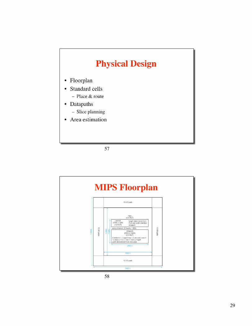
Physical Design
• Floorplan
• Standard cells– Place & route
• Datapaths– Slice planning
• Area estimation
58
MIPS Floorplan
30
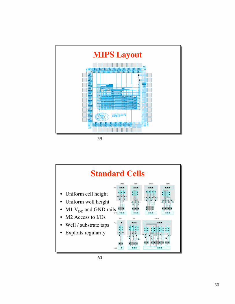
59
MIPS Layout
60
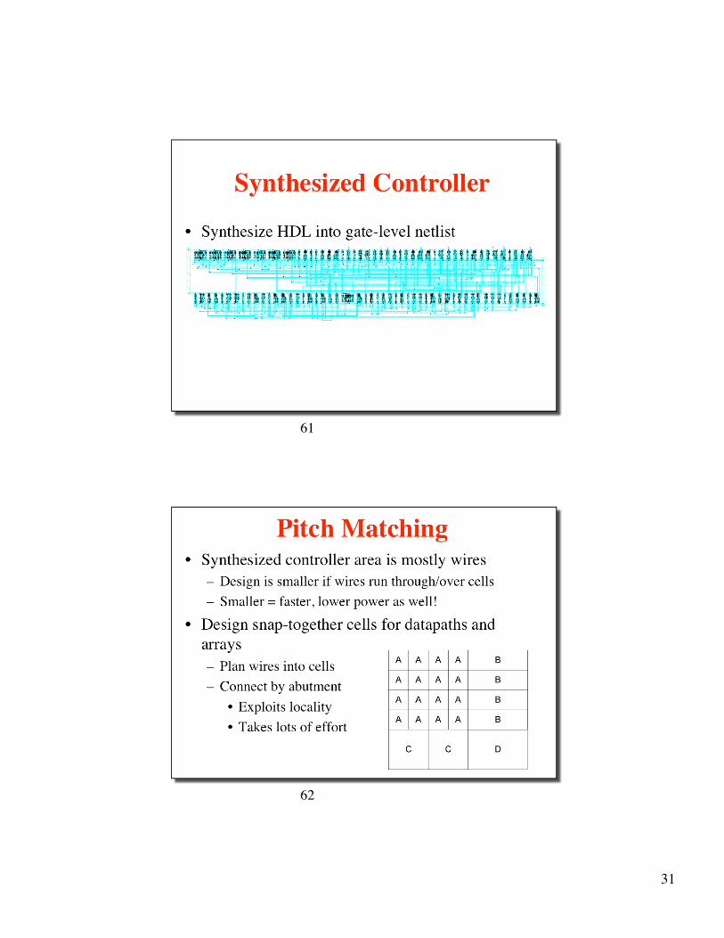
Standard Cells
• Uniform cell height
• Uniform well height
• M1 VDD and GND rails
• M2 Access to I/Os
• Well / substrate taps
• Exploits regularity
31
61
Synthesized Controller
• Synthesize HDL into gate-level netlist
• Place & Route using standard cell library
62
Pitch Matching• Synthesized controller area is mostly wires
– Design is smaller if wires run through/over cells
– Smaller = faster, lower power as well!
• Design snap-together cells for datapaths and arrays– Plan wires into cells
– Connect by abutment
• Exploits locality
• Takes lots of effort

32
63
MIPS Datapath• 8-bit datapath built from 8 bitslices (regularity)
• Zipper at top drives control signals to datapath
64
Slice Plans• Slice plan for bitslice
– Cell ordering, dimensions, wiring tracks
– Arrange cells for wiring locality
33
65
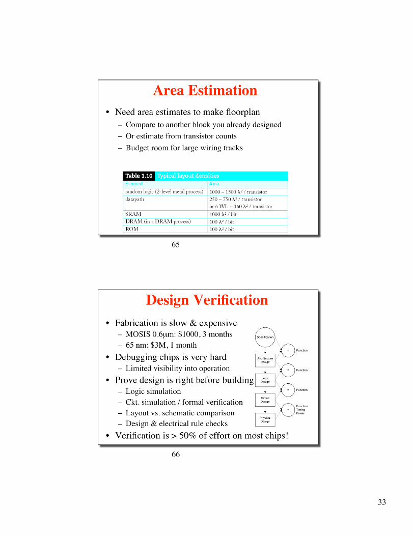
Area Estimation• Need area estimates to make floorplan
– Compare to another block you already designed
– Or estimate from transistor counts
– Budget room for large wiring tracks
66
Design Verification• Fabrication is slow & expensive
– MOSIS 0.6μm: $1000, 3 months– 65 nm: $3M, 1 month
• Debugging chips is very hard– Limited visibility into operation
• Prove design is right before building!– Logic simulation– Ckt. simulation / formal verification– Layout vs. schematic comparison– Design & electrical rule checks
• Verification is > 50% of effort on most chips!
34
67
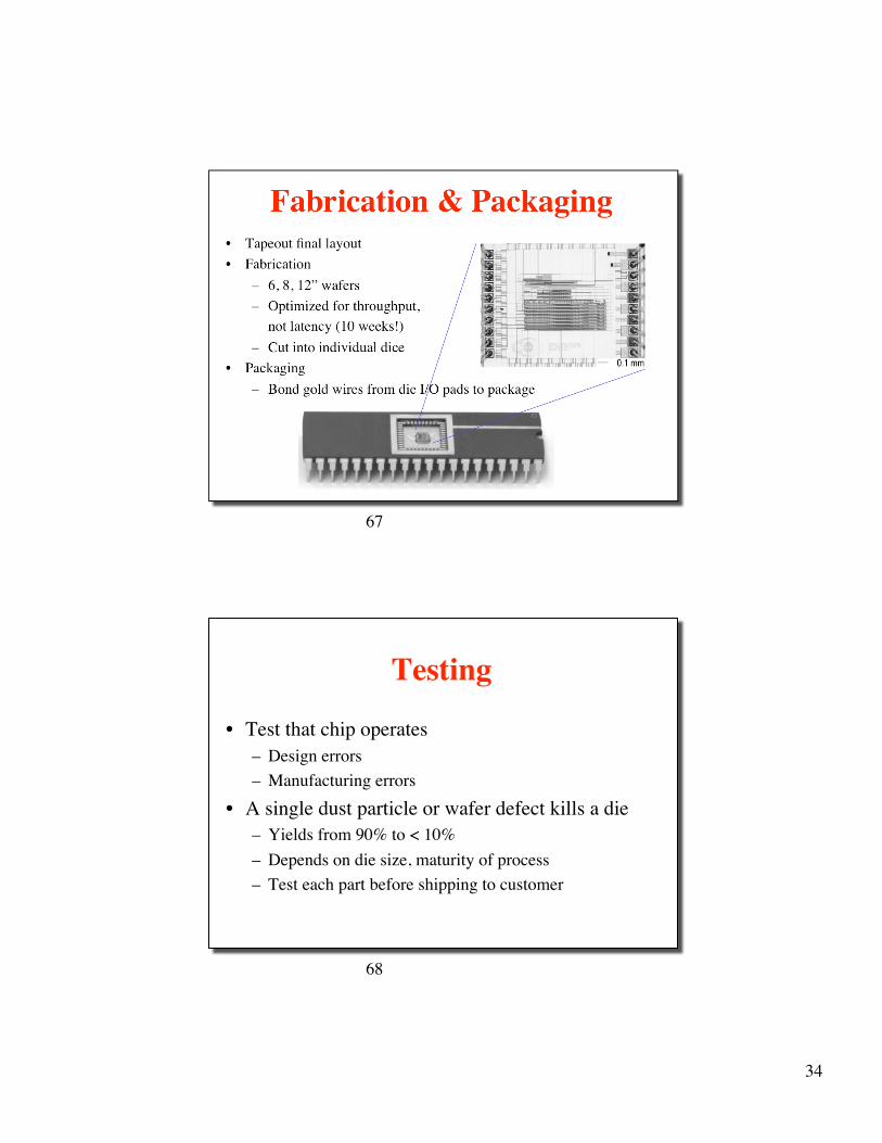
Fabrication & Packaging• Tapeout final layout
• Fabrication
– 6, 8, 12” wafers
– Optimized for throughput,
not latency (10 weeks!)
– Cut into individual dice
• Packaging
– Bond gold wires from die I/O pads to package
68
Testing
• Test that chip operates– Design errors
– Manufacturing errors
• A single dust particle or wafer defect kills a die– Yields from 90% to < 10%
– Depends on die size, maturity of process
– Test each part before shipping to customer