Embed Size (px)
Citation preview
EC6703 - EMBEDDED AND REAL TIME SYSTEMS
UNIT- I
INTRODUCTION TO EMBEDDED COMPUTING
COMPLEX SYSTEMS AND MICROPROCESSORS
An embedded computer system is any device that includes a programmable computer but is not itself intended to be a general-purpose computer. Thus, a PC is not itself an embedded computing system, although PCs are often used to build embedded computing systems. But a fax machine or a clock built from a microprocessor is an embedded computing system.
This means that embedded computing system design is a useful skill for many types of product design. Automobiles, cell phones, and even household appliances make extensive use of microprocessors. Designers in many fields must be able to identify where microprocessors can be used, design a hardware platform with I/O devices that can support the required tasks, and implement software that performs the required processing.
Computer engineering, like mechanical design or thermodynamics, is a fundamental discipline
that can be applied in many different domains. But of course, embedded computing system design does not stand alone. Many of the challenges encountered in the design of an embedded computing system are not computer engineering—for example, they may be mechanical or analog electrical problems.
Embedding Computers
Computers have been embedded into applications since the earliest days of computing. One example is the Whirlwind, a computer designed at MIT in the late 1940s and early 1950s. Whirlwind was also the first computer designed to support real-time operation and was originally conceived as a mechanism for controlling an aircraft simulator.
Even though it was extremely large physically compared to today’s computers (e.g., it
contained over 4,000 vacuum tubes), its complete design from components to system was
attuned to the needs of real-time embedded computing.
The utility of computers in replacing mechanical or human controllers was evident from the
very beginning of the computer era—for example, computers were proposed to control chemical processes in the late 1940s.
A microprocessor is a single-chip CPU. Very large scale integration (VLSI) stet the acronym is
the name technology has allowed us to put a complete CPU on a single chip since 1970s, but those CPUs were very simple.
The first microprocessor, the Intel 4004, was designed for an embedded application, namely, a calculator. The calculator was not a general-purpose computer—it merely provided basic arithmetic functions. However, Ted Hoff of Intel realized that a general-purpose computer programmed properly could implement the required function, and that the computer-on-a-chip could then be reprogrammed for use in other products as well.
Since integrated circuit design was (and still is) an expensive and time consuming process, the
ability to reuse the hardware design by changing the software was a key breakthrough.
The HP-35 was the first handheld calculator to perform transcendental functions [Whi72]. It
was introduced in 1972, so it used several chips to implement the CPU, rather than a single-chip microprocessor.
However, the ability to write programs to perform math rather than having to design digital
circuits to perform operations like trigonometric functions was critical to the successful design of the calculator.
Automobile designers started making use of the microprocessor soon after single-chip CPUs
became available.
The most important and sophisticated use of microprocessors in automobiles was to control the
engine: determining when spark plugs fire, controlling the fuel/air mixture, and so on. There was a trend toward electronics in automobiles in general—electronic devices could be used to replace the mechanical distributor.
But the big push toward microprocessor-based engine control came from two nearly simultaneous developments: The oil shock of the 1970s caused consumers to place much higher value on fuel economy, and fears of pollution resulted in laws restricting automobile engine emissions.
The combination of low fuel consumption and low emissions is very difficult to achieve; to
meet these goals without compromising engine performance, automobile manufacturers turned to sophisticated control algorithms that could be implemented only with microprocessors.
Microprocessors come in many different levels of sophistication; they are usually classified by
their word size. An 8-bit microcontroller is designed for low-cost applications and includes on-
board memory and I/O devices; a 16-bit microcontroller is often used for more sophisticated
applications that may require either longer word lengths or off-chip I/O and memory; and a 32-
bit RISC microprocessor offers very high performance for computation intensive applications.
Given the wide variety of microprocessor types available, it should be no surprise that
microprocessors are used in many ways. There are many household uses of microprocessors. The typical microwave oven has at least one microprocessor to control oven operation.
Many houses have advanced thermostat systems, which change the temperature level at various
times during the day. The modern camera is a prime example of the powerful features that can be added under microprocessor control.
Digital television makes extensive use of embedded processors. In some cases, specialized
CPUs are designed to execute important algorithms—an example is the CPU designed for
audio processing in the SGS Thomson chip set for DirecTV [Lie98]. This processor is designed to efficiently implement programs for digital audio decoding.
A programmable CPU was used rather than a hardwired unit for two reasons: First, it made the
system easier to design and debug; and second, it allowed the possibility of upgrades and using the CPU for other purposes.
A high-end automobile may have 100 microprocessors, but even inexpensive cars today use 40
microprocessors. Some of these microprocessors do very simple things such as detect whether
seat belts are in use. Others control critical functions such as the ignition and braking systems.
BMW 850i brake and stability control system:
The BMW 850i was introduced with a sophisticated system for controlling the wheels of the car. An antilock brake system (ABS) reduces skidding by pumping the brakes.
An automatic stability control (ASC +T) system intervenes with the engine during maneuvering
to improve the car’s stability. These systems actively control critical systems of the car; as control systems, they require inputs from and output to the automobile.
Let’s first look at the ABS. The purpose of an ABS is to temporarily release the brake on a
wheel when it rotates too slowly—when a wheel stops turning, the car starts skidding and
becomes hard to control. It sits between the hydraulic pump, which provides power to the
brakes, and the brakes themselves as seen in the following diagram. This hookup allows the
ABS system to modulate the brakes in order to keep the wheels from locking.
The ABS system uses sensors on each wheel to measure the speed of the wheel. The wheel
speeds are used by the ABS system to determine how to vary the hydraulic fluid pressure to
prevent the wheels from skidding.
The ASC + T system’s job is to control the engine power and the brake to improve the car’s
stability during maneuvers.
The ASC+T controls four different systems: throttle, ignition timing, differential brake, and (on automatic transmission cars) gear shifting.
The ASC + T can be turned off by the driver, which can be important when operating with tire
snow chains.
The ABS and ASC+ T must clearly communicate because the ASC + T interact with the brake
system. Since the ABS was introduced several years earlier than the ASC + T, it was important to be able to interface ASC + T to the existing ABS module, as well as to other existing electronic modules.
The engine and control management units include the electronically controlled throttle, digital engine management, and electronic transmission control. The ASC + T control unit has two microprocessors on two printed circuit boards, one of which concentrates on logic-relevant components and the other on performance-specific components.
Characteristics of Embedded Computing Applications
Embedded computing is in many ways much more demanding than the sort of programs that
you may have written for PCs or workstations. Functionality is important in both general-purpose
computing and embedded computing, but embedded applications must meet many other constraints as
well.
On the one hand, embedded computing systems have to provide sophisticated functionality:
■ Complex algorithms: The operations performed by the microprocessor may be very sophisticated.
For example, the microprocessor that controls an automobile engine must perform complicated filtering
functions to optimize the performance of the car while minimizing pollution and fuel utilization.
■ User interface: Microprocessors are frequently used to control complex user interfaces that may include multiple menus and many options. The moving maps in Global Positioning System (GPS)
navigation are good examples of sophisticated user interfaces.
To make things more difficult, embedded computing operations must often be performed to
meet deadlines:
■ Real time: Many embedded computing systems have to perform in real time— if the data is not
ready by a certain deadline, the system breaks. In some cases, failure to unsafe and can even endanger
lives. In other cases, missing a deadline does not create safety problems but does create unhappy
customers—missed deadlines in printers, for example, can result in scrambled pages.
■ Multirate: Not only must operations be completed by deadlines, but many embedded computing
systems have several real-time activities going on at the same time. They may simultaneously control
some operations that run at slow rates and others that run at high rates. Multimedia applications are
prime examples of multirate behavior. The audio and video portions of a multimedia stream run at very
different rates, but they must remain closely synchronized. Failure to meet a deadline on either the
audio or video portions spoils the perception of the entire presentation.
Costs of various sorts are also very important: ■ Manufacturing cost: The total cost of building the system is very important in many cases.
Manufacturing cost is determined by many factors, including the type of microprocessor used, the
amount of memory required, and the types of I/O devices. ■ Power and energy: Power consumption directly affects the cost of the hardware, since a larger
power supply may be necessary. Energy consumption affects battery life, which is important in many applications, as well as heat consumption, which can be important even in desktop applications.

DESIGN EXAMPLE: MODEL TRAIN CONTROLLER
In order to learn how to use UML to model systems, we will specify a simple system, a model
train controller, which is illustrated in Figure 1.2.The user sends messages to the train with a
control box attached to the tracks.
The control box may have familiar controls such as a throttle, emergency stop button, and so on.
Since the train receives its electrical power from the two rails of the track, the control box can
send signals to the train over the tracks by modulating the power supply voltage. As shown in the
figure, the control panel sends packets over the tracks to the receiver on the train.
The train includes analog electronics to sense the bits being transmitted and a control system to
set the train motor’s speed and direction based on those commands.
Each packet includes an address so that the console can control several trains on the same track;
the packet also includes an error correction code (ECC) to guard against transmission errors.
This is a one-way communication system the model train cannot send commands back to the
user.
We start by analyzing the requirements for the train control system. We will base our system on
a real standard developed for model trains. We then develop two specifications: a simple, high-
level specification and then a more detailed specification.
Requirements:
Before we can create a system specification, we have to understand the requirements.
Here is a basic set of requirements for the system:
The console shall be able to control up to eight trains on a single track.
The speed of each train shall be controllable by a throttle to at least 63 different levels in each direction (forward and reverse).
There shall be an inertia control that shall allow the user to adjust the responsiveness of the train
to commanded changes in speed. Higher inertia means that the train responds more slowly to a
change in the throttle, simulating the inertia of a large train. The inertia control will provide at
least eight different levels.
There shall be an emergency stop button.
An error detection scheme will be used to transmit messages.

We can put the requirements into chart format:
Name Model train controller
Purpose Control speed of up to eight model trains Inputs Throttle, inertia setting, emergency stop, train number
Outputs Train control signals
Functions Set engine speed based upon inertia settings; respond to
emergency stop
Performance Can update train speed at least 10 times per second
Manufacturing cost $50
Power 10W (plugs into wall)
Physical size and weight Console should be comfortable for two hands,
approximate size of standard keyboard; weight<2 pounds
We will develop our system using a widely used standard for model train control. We could develop our own train control system from scratch, but basing our system upon a standard has several advantages in this case: It reduces the amount of work we have to do and it allows us to use a wide variety of existing trains and other pieces of equipment.
DCC:
The Digital Command Control (DCC) was created by the National Model Railroad Association to support interoperable digitally-controlled model trains.
Hobbyists started building homebrew digital control systems in the 1970s and Marklin developed its own digital control system in the 1980s. DCC was created to provide a standard that could be built by any manufacturer so that hobbyists could mix and match components from multiple vendors.
The DCC standard is given in two documents:
Standard S-9.1, the DCC Electrical Standard, defines how bits are encoded on the rails for
transmission. Standard S-9.2, the DCC Communication Standard, defines the packets that carry information.
Any DCC-conforming device must meet these specifications. DCC also provides several recommended practices. These are not strictly required but they provide some hints to manufacturers and users as to how to best use DCC.
The DCC standard does not specify many aspects of a DCC train system. It doesn’t define the
control panel, the type of microprocessor used, the programming language to be used, or many
other aspects of a real model train system.
The standard concentrates on those aspects of system design that are necessary for interoperability. Over standardization, or specifying elements that do not really need to be standardized, only makes the standard less attractive and harder to implement.
The Electrical Standard deals with voltages and currents on the track. While the electrical engineering aspects of this part of the specification are beyond the scope of the book, we will briefly discuss the data encoding here.
The standard must be carefully designed because the main function of the track is to carry power to the locomotives. The signal encoding system should not interfere with power transmission either to DCC or non-DCC locomotives. A key requirement is that the data signal should not change the DC value of the rails.
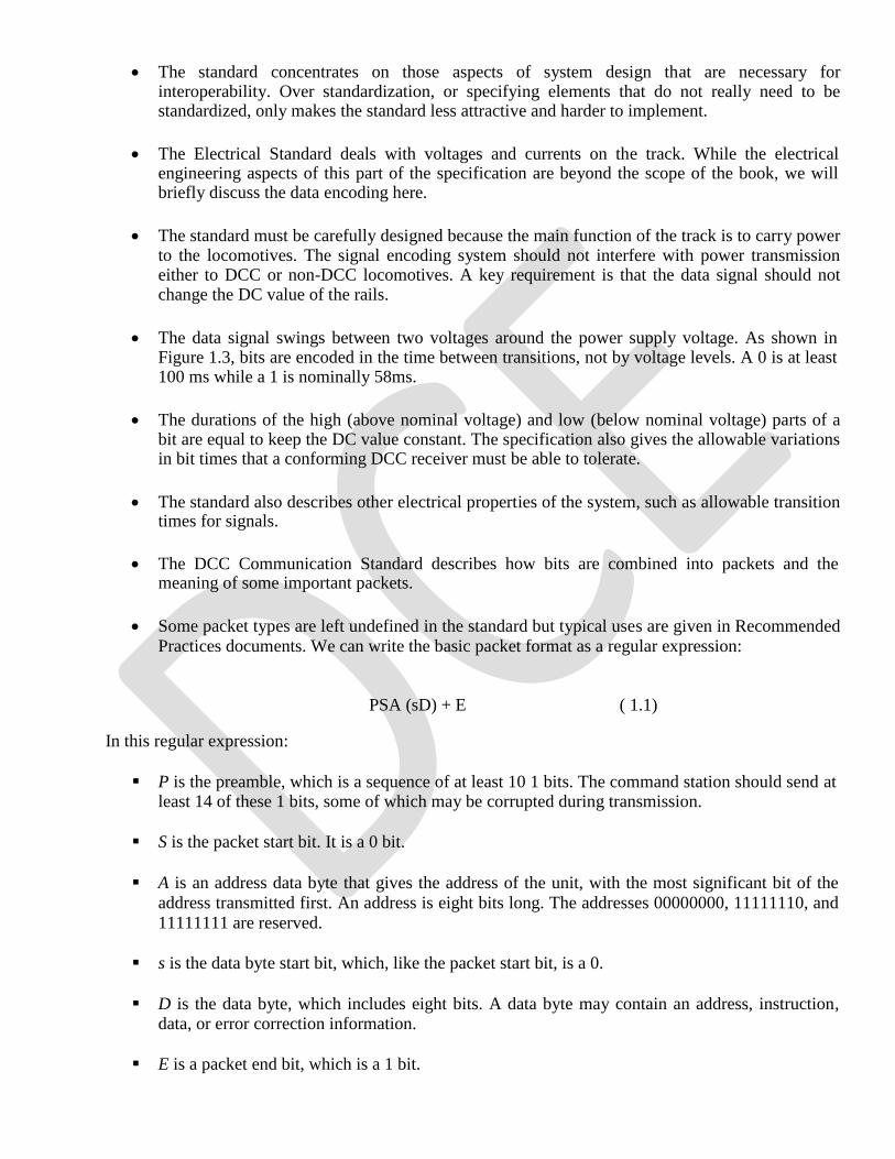
The data signal swings between two voltages around the power supply voltage. As shown in Figure 1.3, bits are encoded in the time between transitions, not by voltage levels. A 0 is at least 100 ms while a 1 is nominally 58ms.
The durations of the high (above nominal voltage) and low (below nominal voltage) parts of a bit are equal to keep the DC value constant. The specification also gives the allowable variations in bit times that a conforming DCC receiver must be able to tolerate.
The standard also describes other electrical properties of the system, such as allowable transition times for signals.
The DCC Communication Standard describes how bits are combined into packets and the meaning of some important packets.
Some packet types are left undefined in the standard but typical uses are given in Recommended
Practices documents. We can write the basic packet format as a regular expression:
PSA (sD) + E ( 1.1) In this regular expression:
P is the preamble, which is a sequence of at least 10 1 bits. The command station should send at
least 14 of these 1 bits, some of which may be corrupted during transmission.
S is the packet start bit. It is a 0 bit.
A is an address data byte that gives the address of the unit, with the most significant bit of the
address transmitted first. An address is eight bits long. The addresses 00000000, 11111110, and
11111111 are reserved.
s is the data byte start bit, which, like the packet start bit, is a 0.
D is the data byte, which includes eight bits. A data byte may contain an address, instruction,
data, or error correction information.
E is a packet end bit, which is a 1 bit.
A packet includes one or more data byte start bit/data byte combinations. Note that the address data byte is a specific type of data byte.
A baseline packet is the minimum packet that must be accepted by all DCC implementations. More complex packets are given in a Recommended Practice document.
A baseline packet has three data bytes: an address data byte that gives the inended receiver of the packet; the instruction data byte provides a basic instruction; and an error correction data byte is used to detect and correct transmission errors.
The instruction data byte carries several pieces of information. Bits 0–3 provide a 4-bit speed
value. Bit 4 has an additional speed bit, which is interpreted as the least significant speed bit. Bit
5 gives direction, with 1 for forward and 0 for reverse. Bits 7–8 are set at 01 to indicate that this
instruction provides speed and direction.
The error correction data byte is the bitwise exclusive OR of the address and instruction data
bytes.
The standard says that the command unit should send packets frequently since a packet may be corrupted. Packets should be separated by at least 5 ms.
Conceptual Specification:
Digital Command Control specifies some important aspects of the system, particularly those that
allow equipment to interoperate. But DCC deliberately does not specify everything about a model train control system. We need to round out our specification with details that complement the DCC spec.
A conceptual specification allows us to understand the system a little better. We will use the
experience gained by writing the conceptual specification to help us write a detailed specification to be given to a system architect. This specification does not correspond to what any commercial DCC controllers do, but it is simple enough to allow us to cover some basic concepts in system design.
A train control system turns commands into packets. A command comes from the command
unit while a packet is transmitted over the rails.
Commands and packets may not be generated in a 1-to-1 ratio. In fact, the DCC standard says
that command units should resend packets in case a packet is dropped during transmission.
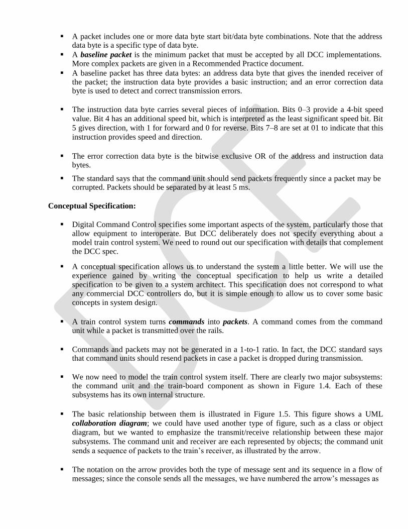
We now need to model the train control system itself. There are clearly two major subsystems:
the command unit and the train-board component as shown in Figure 1.4. Each of these subsystems has its own internal structure.
The basic relationship between them is illustrated in Figure 1.5. This figure shows a UML
collaboration diagram; we could have used another type of figure, such as a class or object
diagram, but we wanted to emphasize the transmit/receive relationship between these major
subsystems. The command unit and receiver are each represented by objects; the command unit
sends a sequence of packets to the train’s receiver, as illustrated by the arrow.
The notation on the arrow provides both the type of message sent and its sequence in a flow of
messages; since the console sends all the messages, we have numbered the arrow’s messages as
1..n. Those messages are of course carried over the track.
Since the track is not a computer component and is purely passive, it does not appear in the
diagram. However, it would be perfectly legitimate to model the track in the collaboration diagram, and in some situations it may be wise to model such nontraditional components in the specification diagrams. For example, if we are worried about what happens when the track breaks, modeling the tracks would help us identify failure modes and possible recovery mechanisms.
UML collaboration diagram for major subsystems of the train controller system.
Let’s break down the command unit and receiver into their major components. The console
needs to perform three functions: read the state of the front panel on the command unit, format
messages, and transmit messages. The train receiver must also perform three major functions: receive
the message, interpret the message (taking into account the current speed, inertia setting, etc.), and
actually control the motor. In this case, let’s use a class diagram to represent the design; we could also
use an object diagram if we wished. The UML class diagram is shown in Figure. It shows the console
class using three classes, one for each of its major components. These classes must define some
behaviors, but for the moment we will concentrate on the basic characteristics of these classes: ■ The Console class describes the command unit’s front panel, which contains the analog knobs and
hardware to interface to the digital parts of the system.
■ The Formatter class includes behaviors that know how to read the panel knobs and creates a bit
stream for the required message.
■ The Transmitter class interfaces to analog electronics to send the message along the track.
There will be one instance of the Console class and one instance of each of the component
classes, as shown by the numeric values at each end of the relationship links. We have also shown some special classes that represent analog components, ending the name of each with an asterisk:
■ Knobs* describes the actual analog knobs, buttons, and levers on the control panel.
■ Sender* describes the analog electronics that send bits along the track.
Likewise, the Train makes use of three other classes that define its components:
■ The Receiver class knows how to turn the analog signals on the track into digital form.
■ The Controller class includes behaviors that interpret the commands and figures out how to control
the motor.
■ The Motor interface class defines how to generate the analog signals required to control the motor.
We define two classes to represent analog components:
■ Detector* detects analog signals on the track and converts them into digital form.
■ Pulser* turns digital commands into the analog signals required to control the motor speed.
We have also defined a special class, Train set, to help us remember that the system can handle
multiple trains. The values on the relationship edge show that one train set can have t trains. We would
not actually implement the train set class, but it does serve as useful documentation of the existence of multiple receivers.
THE EMBEDDED SYSTEM DESIGN PROCESS
The overview of the embedded system design process aimed at two objectives. First, it will give us an introduction to the various steps in embedded system design before we delve into them in more detail. Second, it will allow us to consider the design methodology itself. A design methodology is important for three reasons.
First, it allows us to keep a scorecard on a design to ensure that we have done everything we
need to do, such as optimizing performance or performing functional tests.
Second, it allows us to develop computer-aided design tools. Developing a single program that
takes in a concept for an embedded system and emits a completed design would be a daunting task, but by first breaking the process into manageable steps, we can work on automating (or at least semi automating) the steps one at a time.
Third, a design methodology makes it much easier for members of a design team to
communicate. By defining the overall process, team members can more easily understand what they are supposed to do, what they should receive from other team members at certain times,
and what they are to hand off when they complete their assigned steps. Since most embedded systems are designed by teams, coordination is perhaps the most important role of a well-defined design methodology.
The figure summarizes the major steps in the embedded system design process. In this top–
down view, we start with the system requirements. In the next step, specification, we create a
more detailed description of what we want.
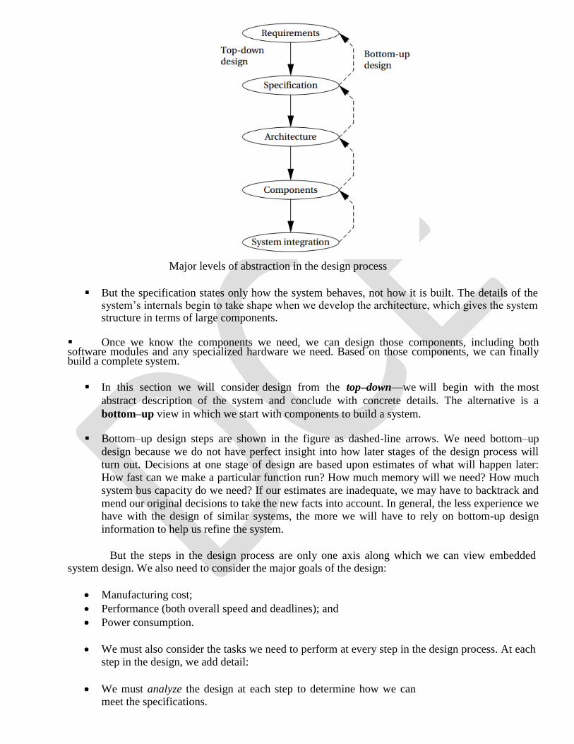
Major levels of abstraction in the design process
But the specification states only how the system behaves, not how it is built. The details of the
system’s internals begin to take shape when we develop the architecture, which gives the system structure in terms of large components.
Once we know the components we need, we can design those components, including both software modules and any specialized hardware we need. Based on those components, we can finally build a complete system.
In this section we will consider design from the top–down—we will begin with the most
abstract description of the system and conclude with concrete details. The alternative is a
bottom–up view in which we start with components to build a system.
Bottom–up design steps are shown in the figure as dashed-line arrows. We need bottom–up
design because we do not have perfect insight into how later stages of the design process will
turn out. Decisions at one stage of design are based upon estimates of what will happen later:
How fast can we make a particular function run? How much memory will we need? How much
system bus capacity do we need? If our estimates are inadequate, we may have to backtrack and
mend our original decisions to take the new facts into account. In general, the less experience we
have with the design of similar systems, the more we will have to rely on bottom-up design
information to help us refine the system.
But the steps in the design process are only one axis along which we can view embedded system design. We also need to consider the major goals of the design:
Manufacturing cost; Performance (both overall speed and deadlines); and Power consumption.
We must also consider the tasks we need to perform at every step in the design process. At each step in the design, we add detail:
We must analyze the design at each step to determine how we can meet the specifications.
We must then refine the design to add detail. We must verify the design to ensure that it still meets all system
goals, such as cost, speed, and so on.
Requirements:
Clearly, before we design a system, we must know what we are designing. The initial stages of
the design process capture this information for use in creating the architecture and components.
We generally proceed in two phases: First, we gather an informal description from the customers
known as requirements, and we refine the requirements into a specification that contains enough information to begin designing the system architecture.
Separating out requirements analysis and specification is often necessary because of the large
gap between what the customers can describe about the system they want and what the architects need to design the system.
Consumers of embedded systems are usually not themselves embedded system designers or even
product designers. Their understanding of the system is based on how they envision users’ interactions with the system. They may have unrealistic expectations as to what can be done within their budgets; and they may also express their desires in
a language very different from
system architects’ jargon.
Capturing a consistent set of requirements from the customer and then massaging those requirements into a more formal specification is a structured way to manage the process of translating from the consumer’s language to the designer’s.
Requirements may be functional or nonfunctional.Wemust of course capture the basic functions of the embedded system,but functional description is often not sufficient.Typical nonfunctional requirements include:
Performance: The speed of the system is often a major consideration both for the usability of the
system and for its ultimate cost. As we have noted, performance may be a combination of soft performance metrics such as approximate time to perform a user-level function and hard deadlines by which a particular operation must be completed.
Cost: The target cost or purchase price for the system is almost always a consideration. Cost
typically has two major components: manufacturing cost includes the cost of components and assembly; nonrecurring engineering (NRE) costs include the personnel and other costs of
designing the system.
Physical size and weight: The physical aspects of the final system can vary greatly depending
upon the application. An industrial control system for an assembly line may be designed to fit into a standard-size rack with no strict limitations on weight. A handheld device typically has
tight requirements on both size and weight that can ripple through the entire system design.
Power consumption: Power, of course, is important in battery-powered systems and is often
important in other applications as well. Power can be specified in the requirements stage in
terms of battery life—the customer is unlikely to be able to describe the allowable wattage.
Validating a set of requirements is ultimately a psychological task since it
requires understanding both what people want and how they communicate those
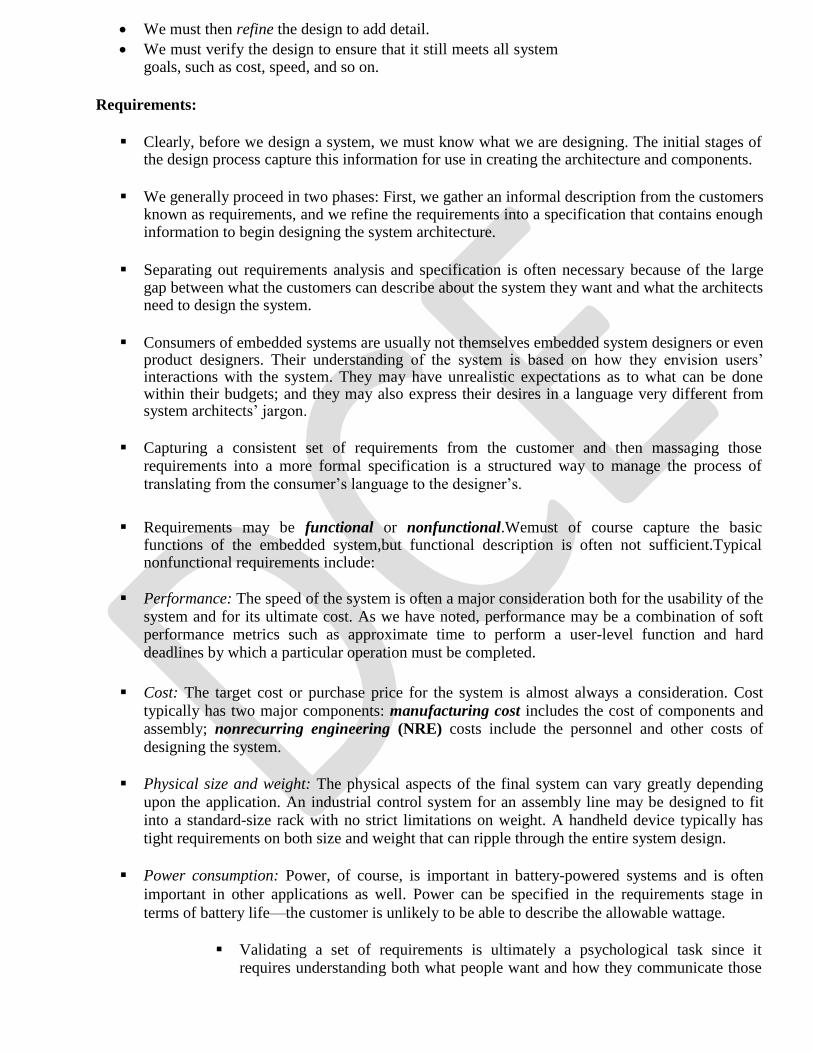
needs. One goodway to refine at least the user interface portion of a system’s requirements is to build a mock-up.
The mock-up may use canned data to simulate functionality in a restricted
demonstration, and it may be executed on a PC or a workstation. But it should give the customer a good idea of how the system will be used and how the user can react to it. Physical, nonfunctional models of devices can also give customers a better idea of characteristics such as size and weight.
Sample requirement form.
Requirements analysis for big systems can be complex and time consuming. However,
capturing a relatively small amount of information in a clear, simple format is a good start toward understanding system requirements.
To introduce the discipline of requirements analysis as part of system design, we will use a
simple requirements methodology.
The figure shows a sample requirements form that can be filled out at the start of the project.
We can use the form as a checklist in considering the basic characteristics of the system.
Let’s consider the entries in the form:
■ Name: This is simple but helpful. Giving a name to the project not only simplifies talking about it to
other people but can also crystallize the purpose of the machine.
■ Purpose: This should be a brief one- or two-line description of what the system is supposed to do. If you can’t describe the essence of your system in one or two lines, chances are that you don’t
understand it well enough.
■ Inputs and outputs: These two entries are more complex than they seem. The inputs and outputs to
the system encompass a wealth of detail: — Types of data: Analog electronic signals? Digital data? Mechanical inputs?
— Data characteristics: Periodically arriving data, such as digital audio samples? Occasional user
inputs? How many bits per data element? — Types of I/O devices: Buttons? Analog/digital converters? Video displays?

■ Functions: This is a more detailed description of what the system does. A good way to approach this
is to work from the inputs to the outputs: When the system receives an input, what does it do? How do user interface inputs affect these functions? How do different functions interact?
■ Performance: Many embedded computing systems spend at least some time controlling physical
devices or processing data coming from the physical world. In most of these cases, the computations
must be performed within a certain time frame. It is essential that the performance requirements be
identified early since they must be carefully measured during implementation to ensure that the
system works properly. ■ Manufacturing cost: This includes primarily the cost of the hardware components. Even if you don’t
know exactly how much you can afford to spend on system components, you should have some idea
of the eventual cost range. Cost has a substantial influence on architecture: A machine that is meant
to sell at $10 most likely has a very different internal structure than a $100 system.
■ Power: Similarly, you may have only a rough idea of how much power the system can consume, but a
little information can go a long way. Typically, the most important decision whether the machine will
be battery powered or plugged into the wall. Battery-powered machines must be much more careful about how they spend energy.
■ Physical size and weight: You should give some indication of the physical size of the system to help
guide certain architectural decisions. A desktop machine has much more flexibility in the components used than, for example, a lapel mounted voice recorder.
Specification
The specification is more precise—it serves as the contract between the customer and the architects. As such, the specification must be carefully written so that it accurately reflects the
customer’s requirements and does so in a way that can be clearly followed during design. Specification is probably the least familiar phase of this methodology for neophyte designers,
but it is essential to creating working systems with a minimum of designer effort. Designers who lack a clear idea of what they want to build when they begin typically make faulty assumptions early in the
process that aren’t obvious until they have a working system. At that point, the only solution is to take
the machine apart, throw away some of it, and start again. Not only does this take a lot of extra time, the resulting system is also very likely to be inelegant, kludgey, and bug-ridden.
The specification should be understandable enough so that someone can verify that it meets system requirements and overall expectations of the customer. It should also be unambiguous enough
that designers know what they need to build. Designers can run into several different types of problems caused by unclear specifications. If the behavior of some feature in a particular situation is
unclear from the specification, the designer may implement the wrong functionality. If global characteristics of the specification are wrong or incomplete, the overall system architecture derived
from the specification may be inadequate to meet the needs of implementation.
A specification of the GPS system would include several components:
■ Data received from the GPS satellite constellation. ■ Map data.
■ User interface. ■ Operations that must be performed to satisfy customer requests.
■ Background actions required to keep the system running, such as operating the GPS receiver. UML, a language for describing specifications, will be introduced in Section 1.3, and we will
use it to write a specification in Section 1.4.We will practice writing specifications in each chapter as
we work through example system designs. We will also study specification techniques in more detail in Chapter 9.
Architecture Design
The specification does not say how the system does things, only what the system does. Describing how the system implements those functions is the purpose of the architecture. The
architecture is a plan for the overall structure of the system that will be used later to design the components that make up the architecture. The creation of the architecture is the first phase of what
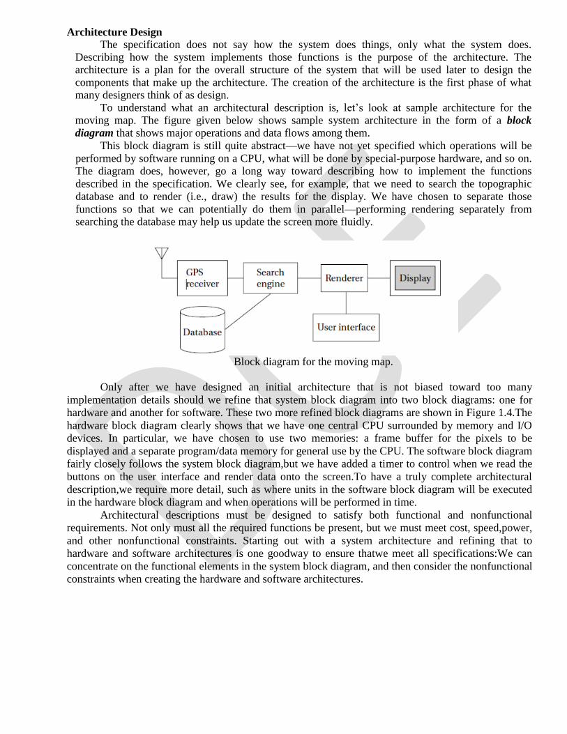
many designers think of as design. To understand what an architectural description is, let’s look at sample architecture for the
moving map. The figure given below shows sample system architecture in the form of a block
diagram that shows major operations and data flows among them.
This block diagram is still quite abstract—we have not yet specified which operations will be
performed by software running on a CPU, what will be done by special-purpose hardware, and so on.
The diagram does, however, go a long way toward describing how to implement the functions
described in the specification. We clearly see, for example, that we need to search the topographic
database and to render (i.e., draw) the results for the display. We have chosen to separate those
functions so that we can potentially do them in parallel—performing rendering separately from
searching the database may help us update the screen more fluidly.
Block diagram for the moving map.
Only after we have designed an initial architecture that is not biased toward too many
implementation details should we refine that system block diagram into two block diagrams: one for
hardware and another for software. These two more refined block diagrams are shown in Figure 1.4.The
hardware block diagram clearly shows that we have one central CPU surrounded by memory and I/O
devices. In particular, we have chosen to use two memories: a frame buffer for the pixels to be
displayed and a separate program/data memory for general use by the CPU. The software block diagram
fairly closely follows the system block diagram,but we have added a timer to control when we read the
buttons on the user interface and render data onto the screen.To have a truly complete architectural
description,we require more detail, such as where units in the software block diagram will be executed
in the hardware block diagram and when operations will be performed in time.
Architectural descriptions must be designed to satisfy both functional and nonfunctional
requirements. Not only must all the required functions be present, but we must meet cost, speed,power,
and other nonfunctional constraints. Starting out with a system architecture and refining that to
hardware and software architectures is one goodway to ensure thatwe meet all specifications:We can
concentrate on the functional elements in the system block diagram, and then consider the nonfunctional
constraints when creating the hardware and software architectures.
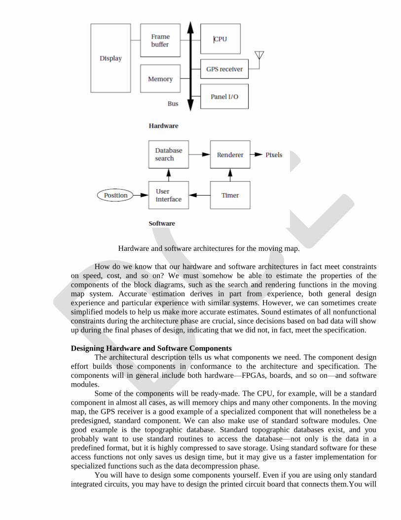
Hardware and software architectures for the moving map.
How do we know that our hardware and software architectures in fact meet constraints
on speed, cost, and so on? We must somehow be able to estimate the properties of the
components of the block diagrams, such as the search and rendering functions in the moving
map system. Accurate estimation derives in part from experience, both general design
experience and particular experience with similar systems. However, we can sometimes create
simplified models to help us make more accurate estimates. Sound estimates of all nonfunctional
constraints during the architecture phase are crucial, since decisions based on bad data will show
up during the final phases of design, indicating that we did not, in fact, meet the specification.
Designing Hardware and Software Components
The architectural description tells us what components we need. The component design
effort builds those components in conformance to the architecture and specification. The
components will in general include both hardware—FPGAs, boards, and so on—and software
modules.
Some of the components will be ready-made. The CPU, for example, will be a standard
component in almost all cases, as will memory chips and many other components. In the moving
map, the GPS receiver is a good example of a specialized component that will nonetheless be a
predesigned, standard component. We can also make use of standard software modules. One
good example is the topographic database. Standard topographic databases exist, and you
probably want to use standard routines to access the database—not only is the data in a
predefined format, but it is highly compressed to save storage. Using standard software for these
access functions not only saves us design time, but it may give us a faster implementation for
specialized functions such as the data decompression phase.
You will have to design some components yourself. Even if you are using only standard
integrated circuits, you may have to design the printed circuit board that connects them.You will

probably have to do a lot of custom programming as well. When creating these embedded
software modules, you must of course make use of your expertise to ensure that the system runs
properly in real time and that it does not take up more memory space than is allowed. The power
consumption of the moving map software example is particularly important. You may need to be
very careful about how you read and write memory to minimize power—for example, since
memory accesses are a major source of power consumption, memory transactions must be
carefully planned to avoid reading the same data several times.
System Integration
Only after the components are built do we have the satisfaction of putting them together
and seeing a working system. Of course, this phase usually consists of a lot more than just
plugging everything together and standing back. Bugs are typically found during system
integration, and good planning can help us find the bugs quickly. By building up the system in
phases and running properly chosen tests, we can often find bugs more easily. If we debug only
a few modules at a time, we are more likely to uncover the simple bugs and able to easily
recognize them. Only by fixing the simple bugs early will we be able to uncover the more
complex or obscure bugs that can be identified only by giving the system a hard workout. We
need to ensure during the architectural and component design phases that we make it as easy as
possible to assemble the system in phases and test functions relatively independently.
System integration is difficult because it usually uncovers problems. It is often hard to
observe the system in sufficient detail to determine exactly what is wrong—the debugging
facilities for embedded systems are usually much more limited than what you would find on
desktop systems. As a result, determining why things do not stet work correctly and how they
can be fixed is a challenge in itself. Careful attention to inserting appropriate debugging
facilities during design can help ease system integration problems, but the nature of embedded
computing means that this phase will always be a challenge.
FORMALISMS FOR SYSTEM DESIGN:
Visual language that can be used to capture all these design tasks: the Unified Modeling
Language (UML). UML was designed to be useful at many levels of abstraction in the design process.
UML is useful because it encourages design by successive refinement and progressively adding detail to
the design, rather than rethinking the design at each new level of abstraction.
UML is an object-oriented modeling language. We will see precisely what we mean by an object
in just a moment, but object-oriented design emphasizes two concepts of importance:
■ It encourages the design to be described as a number of interacting objects, rather than a few large
monolithic blocks of code.
■ At least some of those object will correspond to real pieces of software or hardware in the system. We
can also use UML to model the outside world that interacts with our system, in which case the
objects may correspond to people or other machines. It is sometimes important to implement
something we think of at a high level as a single object using several distinct pieces of code or to
otherwise break up the object correspondence in the implementation However; thinking of the design
in terms of actual objects helps us understand the natural structure of the system. Object-oriented
(often abbreviated OO) specification can be seen in two complementary ways:
■ Object-oriented specification allows a system to be described in a way that closely models real-world
objects and their interactions.

■ Object-oriented specification provides a basic set of primitives that can be used to describe systems with particular attributes, irrespective of the relationships of those systems’ components to real-world
objects.
Both views are useful. At a minimum, object-oriented specification is a set of linguistic
mechanisms. In many cases, it is useful to describe a system in terms of real-world analogs. However,
performance, cost, and so on may dictate that we change the specification to be different in some ways
from the real-world elements we are trying to model and implement. In this case, the object-oriented
specification mechanisms are still useful.
A specification language may not be executable. But both object-oriented specification and
programming languages provide similar basic methods for structuring large systems.
Unified Modeling Language (UML)—the acronym is the name is a large language, and covering
all of it is beyond the scope of this book. In this section, we introduce only a few basic concepts. In later
chapters, as we need a few more UML concepts, we introduce them to the basic modeling elements
introduced here.
Because UML is so rich, there are many graphical elements in a UML diagram. It is important
to be careful to use the correct drawing to describe something for instance; UML distinguishes between
arrows with open and filled-in arrowheads, and solid and broken lines. As you become more familiar with the language, uses of the graphical primitives will become more natural to you.
We also won’t take a strict object-oriented approach. We may not always use objects for
certain elements of a design—in some cases, such as when taking particular aspects of the
implementation into account, it may make sense to use another design style. However, object-oriented
design is widely applicable, and no designer can consider himself or herself design literate without
understanding it.
Structural Description:
By structural description, we mean the basic components of the system; we will learn how to
describe how these components act in the next section. The principal component of an object-oriented design is, naturally enough, the object. An object includes a set of attributes that define its internal state.
When implemented in a programming language, these attributes usually become variables or
constants held in a data structure. In some cases, we will add the type of the attribute after the attribute name for clarity, but we do not always have to specify a type for an attribute. An object describing a display (such as a CRT screen) is shown in UML notation in Figure 1.8 a).
The text in the folded-corner page icon is a note; it does not correspond to an object in the
system and only serves as a comment. The attribute is, in this case, an array of pixels that holds the contents of the display. The object is identified in two ways: It has a unique name, and it is a member of a class. The name is underlined to show that this is a description of an object and not of a class.
A class is a form of type definition—all objects derived from the same class have the same
characteristics, although their attributes may have different values. A class defines the attributes
that an object may have. It also defines the operations that determine how the object interacts
with the rest of the world. In a programming language, the operations would become pieces of
code used to manipulate the object.
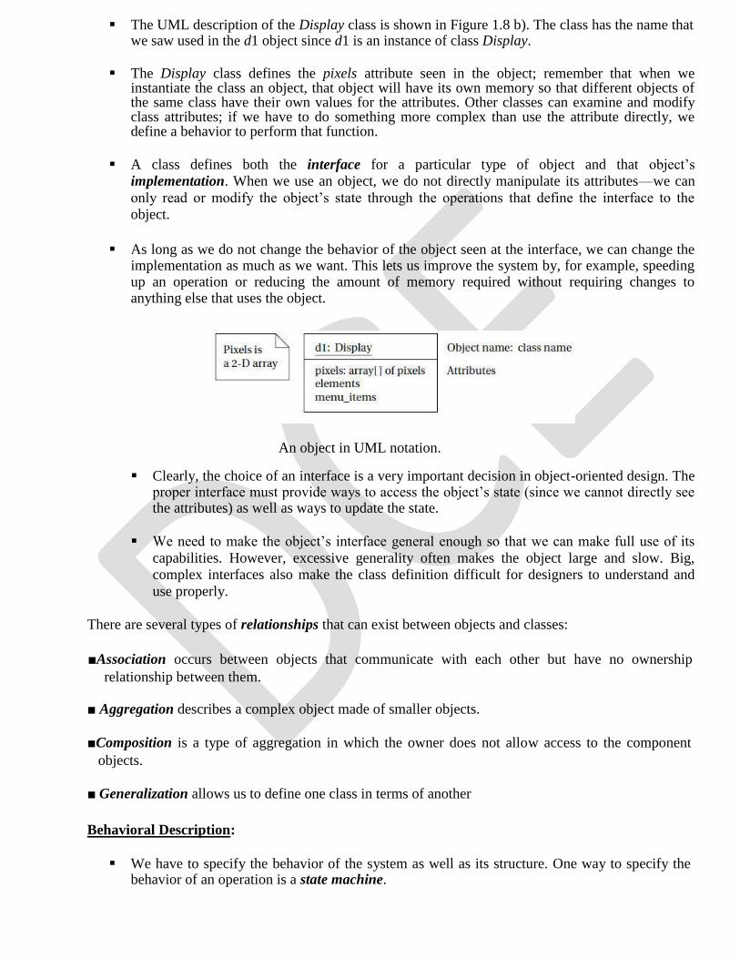
The UML description of the Display class is shown in Figure 1.8 b). The class has the name that we saw used in the d1 object since d1 is an instance of class Display.
The Display class defines the pixels attribute seen in the object; remember that when we
instantiate the class an object, that object will have its own memory so that different objects of the same class have their own values for the attributes. Other classes can examine and modify class attributes; if we have to do something more complex than use the attribute directly, we define a behavior to perform that function.
A class defines both the interface for a particular type of object and that object’s
implementation. When we use an object, we do not directly manipulate its attributes—we can
only read or modify the object’s state through the operations that define the interface to the
object.
As long as we do not change the behavior of the object seen at the interface, we can change the implementation as much as we want. This lets us improve the system by, for example, speeding up an operation or reducing the amount of memory required without requiring changes to anything else that uses the object.
An object in UML notation.
Clearly, the choice of an interface is a very important decision in object-oriented design. The proper interface must provide ways to access the object’s state (since we cannot directly see the attributes) as well as ways to update the state.
We need to make the object’s interface general enough so that we can make full use of its
capabilities. However, excessive generality often makes the object large and slow. Big,
complex interfaces also make the class definition difficult for designers to understand and
use properly.
There are several types of relationships that can exist between objects and classes:
■Association occurs between objects that communicate with each other but have no ownership
relationship between them. ■ Aggregation describes a complex object made of smaller objects.
■Composition is a type of aggregation in which the owner does not allow access to the component
objects.
■ Generalization allows us to define one class in terms of another
Behavioral Description:
We have to specify the behavior of the system as well as its structure. One way to specify the
behavior of an operation is a state machine.
These state machines will not rely on the operation of a clock, as in hardware; rather, changes from one state to another are triggered by the occurrence of events.
An event is some type of action. The event may originate outside the system, such as a user
pressing a button. It may also originate inside, such as when one routine finishes its computation and passes the result on to another routine.We will concentrate on the following three types of events defined by UML,
■ A signal is an asynchronous occurrence. It is defined in UML by an object that is labeled as a
<<signal>>. The object in the diagram serves as a declaration of the event’s existence. Because it is
an object, a signal may have parameters that are passed to the signal’s receiver. ■ A call event follows the model of a procedure call in a programming language.
■A time-out event causes the machine to leave a state after a certain amount of time. The label tm (time-
value) on the edge gives the amount of time after which the transition occurs. A time-out is generally
implemented with an external timer. This notation simplifies the specification and allows us to defer
implementation details about the time-out mechanism.
INSTRUCTION SETS PRELIMINERIS:
Computer Architecture Taxonomy
Before we delve into the details of microprocessor instruction sets, it is helpful to develop some basic terminology. We do so by reviewing taxonomy of the basic ways we can organize a computer.
A block diagram for one type of computer is shown in Figure 1.9. The computing system
consists of a central processing unit (CPU) and a memory.
The memory holds both data and instructions, and can be read or written when given an
address. A computer whose memory holds both data and instructions is known as a von Neumann machine.
The CPU has several internal registers that store values used internally. One of those registers
is the program counter (PC), which holds the address in memory of an instruction. The CPU fetches the instruction from memory, decodes the instruction, and executes it.
The program counter does not directly determine what the machine does next, but only indirectly by pointing to an instruction in memory. By changing only the instructions, we can change what the CPU does. It is this separation of the instruction memory from the CPU that distinguishes a stored-program computer from a general finite-state machine.
An alternative to the von Neumann style of organizing computers is the Harvard
architecture, which is nearly as old as the von Neumann arch itecture. As shown in Figure, a
Harvard machine has separate memories for data and program.
The program counter points to program memory, not data memory. As a result, it is harder to
write self-modifying programs (programs that write data values, and then use those values as instructions) on Harvard machines.
Harvard architectures are widely used today for one very simple reason—the separation of
program and data memories provides higher performance for digital signal processing.
Processing signals in real-time places great strains on the data access system in two ways: First, large amounts of data flow through the CPU; and second, that data must be processed at precise intervals, not just when the CPU gets around to it. Data sets that arrive continuously and periodically are called streaming data.
Having two memories with separate ports provides higher memory bandwidth; not making data
and memory compete for the same port also makes it easier to move the data at the proper times. DSPs constitute a large fraction of all microprocessors sold today, and most of them are Harvard architectures.
A single example shows the importance of DSP: Most of the telephone calls in the world go
through at least two DSPs, one at each end of the phone call.
Another axis along which we can organize computer architectures relates to their instructions and how they are executed. Many early computer architectures were what is known today as complex instruction set computers (CISC). These machines provided a variety of instructions
that may perform very complex tasks, such as string searching; they also generally used a number of different instruction formats of varying lengths.
One of the advances in the development of high-performance microprocessors was the concept
of reduced instruction set computers (RISC).These computers tended to provide somewhat fewer and simpler instructions.
The instructions were also chosen so that they could be efficiently executed in pipelined
processors. Early RISC designs substantially outperformed CISC designs of the period. As it turns out, we can use RISC techniques to efficiently execute at least a common subset of CISC instruction sets, so the performance gap between RISC-like and CISC-like instruction sets has narrowed somewhat.
Beyond the basic RISC/CISC characterization, we can classify computers by several characteristics of their instruction sets. The instruction set of the computer defines the interface between software modules and the underlying hardware; the instructions define what the hardware will do under certain circumstances. Instructions can have a variety of characteristics, including:
o Fixed versus variable length.
o Addressing modes.
o Numbers of operands.
o Types of operations supported.
The set of registers available for use by programs is called the programming model, also known
as the programmer model. (The CPU has many other registers that are used for internal operations
and are unavailable to programmers.)
There may be several different implementations of architecture. In fact, the architecture definition serves to define those characteristics that must be true of all implementations and what may vary from implementation to implementation.
Different CPUs may offer different clock speeds, different cache configurations, changes to the bus or interrupt lines, and many other changes that can make one model of CPU more attractive than another for any given application.
Assembly Language
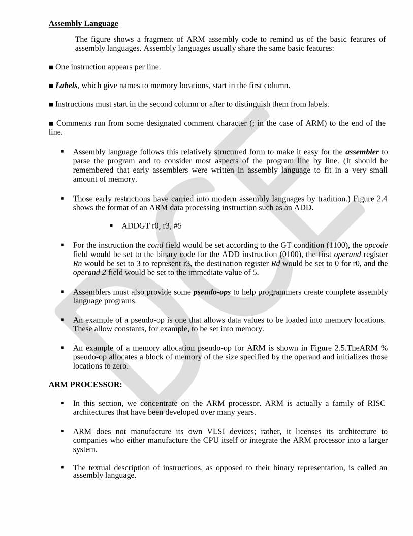
The figure shows a fragment of ARM assembly code to remind us of the basic features of assembly languages. Assembly languages usually share the same basic features:
■ One instruction appears per line.
■ Labels, which give names to memory locations, start in the first column.
■ Instructions must start in the second column or after to distinguish them from labels.
■ Comments run from some designated comment character (; in the case of ARM) to the end of the line.
Assembly language follows this relatively structured form to make it easy for the assembler to parse the program and to consider most aspects of the program line by line. (It should be remembered that early assemblers were written in assembly language to fit in a very small amount of memory.
Those early restrictions have carried into modern assembly languages by tradition.) Figure 2.4
shows the format of an ARM data processing instruction such as an ADD.
ADDGT r0, r3, #5
For the instruction the cond field would be set according to the GT condition (1100), the opcode
field would be set to the binary code for the ADD instruction (0100), the first operand register Rn would be set to 3 to represent r3, the destination register Rd would be set to 0 for r0, and the operand 2 field would be set to the immediate value of 5.
Assemblers must also provide some pseudo-ops to help programmers create complete assembly
language programs.
An example of a pseudo-op is one that allows data values to be loaded into memory locations.
These allow constants, for example, to be set into memory.
An example of a memory allocation pseudo-op for ARM is shown in Figure 2.5.TheARM %
pseudo-op allocates a block of memory of the size specified by the operand and initializes those locations to zero.
ARM PROCESSOR:
In this section, we concentrate on the ARM processor. ARM is actually a family of RISC
architectures that have been developed over many years.
ARM does not manufacture its own VLSI devices; rather, it licenses its architecture to
companies who either manufacture the CPU itself or integrate the ARM processor into a larger system.
The textual description of instructions, as opposed to their binary representation, is called an
assembly language.
ARM instructions are written one per line, starting after the first column. Comments begin with a semicolon and continue to the end of the line. A label, which gives a name to a memory location, comes at the beginning of the line, starting in the first column. Here is an example:
LDR r0, [r8]; a comment
label ADD r4,r0,r1
Processor and Memory Organization:
Different versions of the ARM architecture are identified by different numbers. ARM7 is a von
Neumann architecture machine, while ARM9 uses Harvard architecture.
However, this difference is invisible to the assembly language programmer, except for possible
performance differences. The ARM architecture supports two basic types of data:
The standard ARM word is 32 bits long.
The word may be divided into four 8-bit bytes.
ARM7 allows addresses up to 32 bits long. An address refers to a byte, not a word. Therefore,
the word 0 in the ARM address space is at location 0, the word 1 is at 4, the word 2 is at 8, and so on. (As a result, the PC is incremented by 4 in the absence of a branch.)
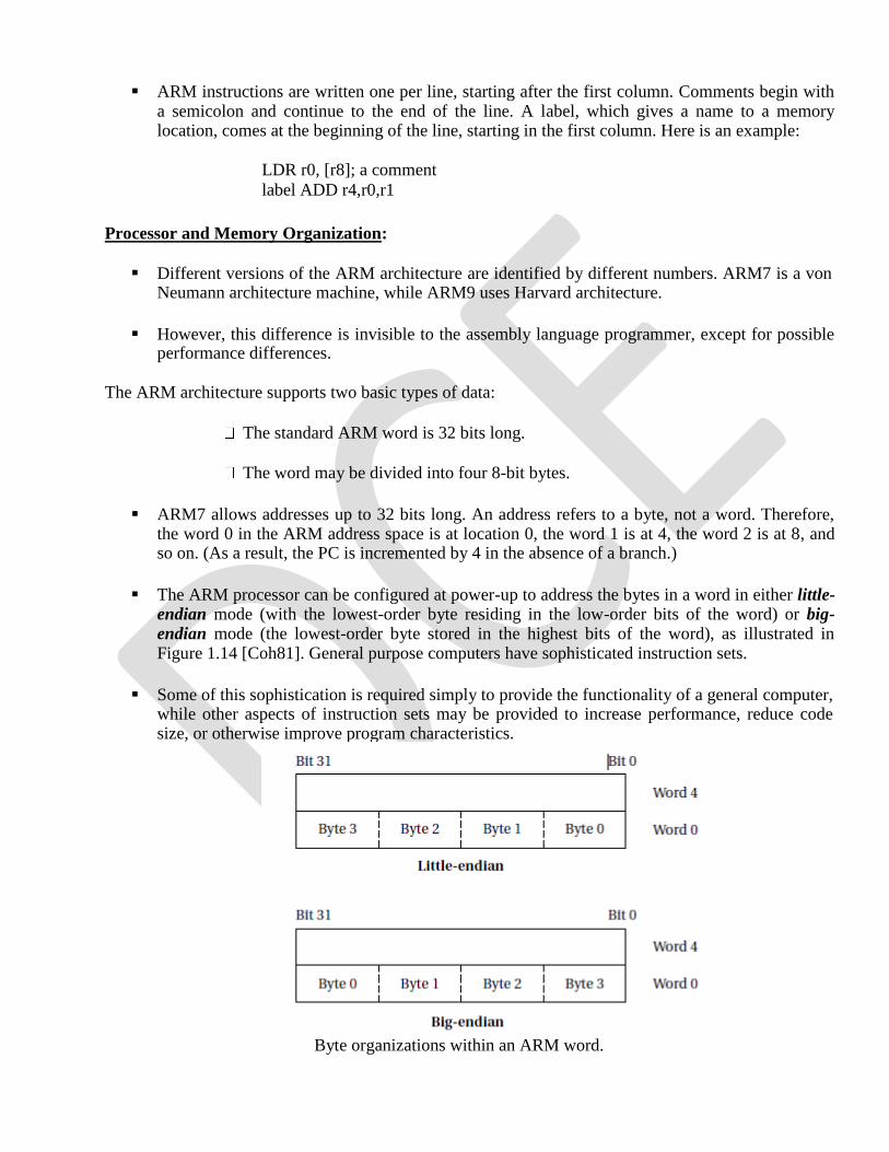
The ARM processor can be configured at power-up to address the bytes in a word in either little-endian mode (with the lowest-order byte residing in the low-order bits of the word) or big-
endian mode (the lowest-order byte stored in the highest bits of the word), as illustrated in
Figure 1.14 [Coh81]. General purpose computers have sophisticated instruction sets.
Some of this sophistication is required simply to provide the functionality of a general computer,
while other aspects of instruction sets may be provided to increase performance, reduce code size, or otherwise improve program characteristics.
Byte organizations within an ARM word.
Data Operations:
Arithmetic and logical operations in C are performed in variables. Variables are implemented as
memory locations. Therefore, to be able to write instructions to perform C expressions and assignments, we must consider both arithmetic and logical instructions as well as instructions for reading and writing memory.
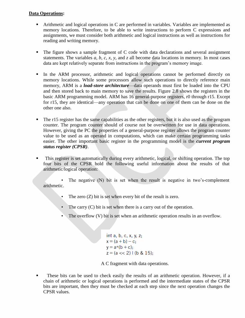
The figure shows a sample fragment of C code with data declarations and several assignment
statements. The variables a, b, c, x, y, and z all become data locations in memory. In most cases data are kept relatively separate from instructions in the program’s memory image.
In the ARM processor, arithmetic and logical operations cannot be performed directly on
memory locations. While some processors allow such operations to directly reference main
memory, ARM is a load-store architecture—data operands must first be loaded into the CPU
and then stored back to main memory to save the results. Figure 2.8 shows the registers in the
basic ARM programming model. ARM has 16 general-purpose registers, r0 through r15. Except
for r15, they are identical—any operation that can be done on one of them can be done on the
other one also.
The r15 register has the same capabilities as the other registers, but it is also used as the program counter. The program counter should of course not be overwritten for use in data operations. However, giving the PC the properties of a general-purpose register allows the program counter value to be used as an operand in computations, which can make certain programming tasks easier. The other important basic register in the programming model is the current program
status register (CPSR).
This register is set automatically during every arithmetic, logical, or shifting operation. The top four bits of the CPSR hold the following useful information about the results of that arithmetic/logical operation:
• The negative (N) bit is set when the result is negative in two’s-complement
arithmetic.
• The zero (Z) bit is set when every bit of the result is zero.
• The carry (C) bit is set when there is a carry out of the operation.
• The overflow (V) bit is set when an arithmetic operation results in an overflow.
A C fragment with data operations.
These bits can be used to check easily the results of an arithmetic operation. However, if a chain of arithmetic or logical operations is performed and the intermediate states of the CPSR bits are important, then they must be checked at each step since the next operation changes the CPSR values.
The basic form of a data instruction is simple:
ADD r0,r1,r2
This instruction sets register r0 to the sum of the values stored in r1 and r2. In addition to
specifying registers as sources for operands, instructions may also provide immediate operands,
which encode a constant value directly in the instruction. For example,
ADD r0,r1,#2 sets r0 to 1+2.
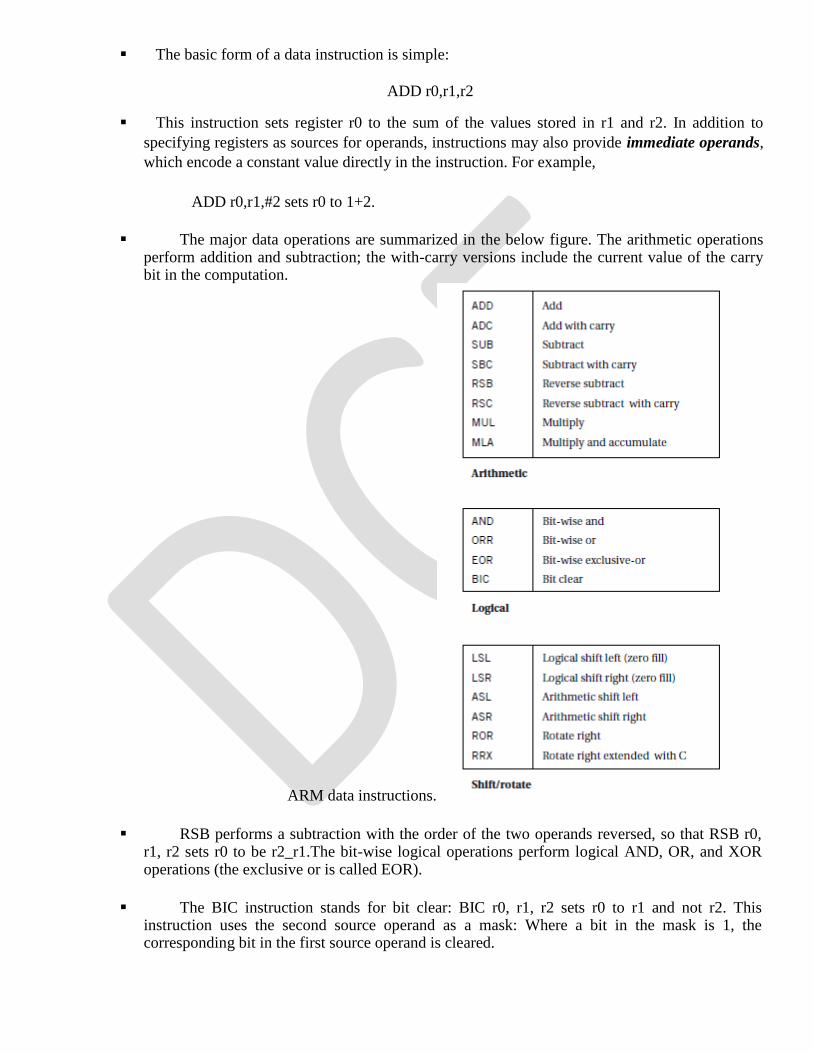
The major data operations are summarized in the below figure. The arithmetic operations perform addition and subtraction; the with-carry versions include the current value of the carry bit in the computation.
ARM data instructions.
RSB performs a subtraction with the order of the two operands reversed, so that RSB r0, r1, r2 sets r0 to be r2_r1.The bit-wise logical operations perform logical AND, OR, and XOR operations (the exclusive or is called EOR).
The BIC instruction stands for bit clear: BIC r0, r1, r2 sets r0 to r1 and not r2. This
instruction uses the second source operand as a mask: Where a bit in the mask is 1, the corresponding bit in the first source operand is cleared.
The MUL instruction multiplies two values, but with some restrictions: No operand may be an immediate, and the two source operands must be different registers.
The MLA instruction performs a multiply-accumulate operation, particularly useful in
matrix operations and signal processing. The instruction
MLA r0, r1, r2, r3
Sets r0 to the value r1*r2+r3. The shift operations are not separate instructions rather; shifts can be applied to arithmetic and
logical instructions. The shift modifier is always applied to the second source operand.
A left shift moves bits up toward the most-significant bits, while a right shift moves bits down to
the least-significant bit in the word.
The LSL and LSR modifiers perform left and right logical shifts, filling the least-significant bits of the operand with zeroes. The arithmetic shift left is equivalent to an LSL, but the ASR copies
the sign bit—if the sign is 0, a 0 is copied, while if the sign is 1, a 1 is copied.
The rotate modifiers always rotate right, moving the bits that fall off the least-significant bit up
to the most-significant bit in the word. The RRX modifier performs a 33-bit rotate, with the CPSR’s C bit being inserted above the sign bit of the word; this allows the carry bit to be included in the rotation.
Programming input and output:
The basic techniques for I/O programming can be understood relatively independent of the
instruction set. In this section, we cover the basics of I/O programming and place them in the contexts of both the ARM and C55x.
We begin by discussing the basic characteristics of I/O devices so that we can understand the
requirements they place on programs that communicate with them. Input and Output Devices:
Input and output devices usually have some analog or non-electronic component for instance, a
disk drive has a rotating disk and analog read/write electronics. But the digital logic in the device that is most closely connected to the CPU very strongly resembles the logic you would expect in any computer system.
The figure shows the structure of a typical I/O device and its relationship to the CPU.The
interface between the CPU and the device’s internals (e.g.,the rotating disk and read/write electronics in a disk drive) is a set of registers. The CPU talks to the device by reading and writing the registers.
Devices typically have several registers:
Data registers hold values that are treated as data by the device, such as the data read or
written by a disk.
Status registers provide information about the device’s operation, such as whether the
current transaction has completed. Some registers may be read-only, such as a status register that indicates when the device is
done, while others may be readable or writable.
Input and Output Primitives:
Microprocessors can provide programming support for input and output in two ways: I/O
instructions and memory-mapped I/O.
Some architectures, such as the Intel x86, provide special instructions (in and out in the case of
the Intel x86) for input and output. These instructions provide a separate address space for I/O devices.
But the most common way to implement I/O is by memory mapping even CPUs that provide
I/O instructions can also implement memory-mapped I/O.
As the name implies, memory-mapped I/O provides addresses for the registers in each I/O
device. Programs use the CPU’s normal read and write instructions to communicate with the devices.
Busy-Wait I/O:
The most basic way to use devices in a program is busy-wait I/O. Devices are typically slower
than the CPU and may require many cycles to complete an operation. If the CPU is performing multiple operations on a single device, such as writing several characters to an output device, then it must wait
for one operation to complete before starting the next one. (If we try to start writing the second character before the device has finished with the first one, for example, the device will probably never
print the first character.) Asking an I/O device whether it is finished by reading its status register is
often called polling.
SUPERVISOR MODE, EXCEPTIONS, AND TRAPS:
These are mechanisms to handle internal conditions, and they are very similar to interrupts in form.
We begin with a discussion of supervisor mode, which some processors use to handle exceptional events and protect executing programs from each other.
Supervisor Mode:
As will become clearer in later chapters, complex systems are often implemented as several
programs that communicate with each other. These programs may run under the command of an operating system. It may be desirable to provide hardware checks to
we
wn
ws
.u
anrne
auntih
vea
rztity
t.h
coe
m
programs do not interfere with each other—for example, by erroneously writing into a segment of memory used by another program. Software debugging is important but can leave some problems in a running system; hardware checks ensure an additional level of safety.
In such cases it is often useful to have a supervisor mode provided by the CPU. Normal programs
run in user mode. The supervisor mode has privileges that user modes do not. Control of the memory
management unit (MMU) is typically reserved for supervisor mode to avoid the obvious problems that
could occur when program bugs cause inadvertent changes in the memory management registers.
Not all CPUs have supervisor modes. Many DSPs, including the C55x, do not provide supervisor modes. The ARM, however, does have such a mode. The ARM instruction that puts the CPU in supervisor mode is called SWI:
SWI CODE_1
It can, of course, be executed conditionally, as with any ARM instruction. SWI causes the CPU
to go into supervisor mode and sets the PC to 0x08.The argument to SWI is a 24-bit immediate value
that is passed on to the supervisor mode code; it allows the program to request various services from the
supervisor mode.
In supervisor mode, the bottom 5 bits of the CPSR are all set to 1 to indicate that the CPU is in supervisor mode. The old value of the CPSR just before the SWI is stored in a register called the saved
program status register (SPSR). There are in fact several SPSRs for different modes; the supervisor
mode SPSR is referred to as SPSR_svc.
To return from supervisor mode, the supervisor restores the PC from register r14 and restores
the CPSR from the SPSR_svc.
Exceptions:
An exception is an internally detected error. A simple example is division by zero. One way to
handle this problem would be to check every divisor before division to be sure it is not zero, but
this would both substantially increase the size of numerical programs and cost a great deal of
CPU time evaluating the divisor’s value.
The CPU can more efficiently check the divisor’s value during execution. Since the time at
which a zero divisor will be found is not known in advance, this event is similar to an interrupt
except that it is generated inside the CPU. The exception mechanism provides a way for the
program to react to such unexpected events.
Just as interrupts can be seen as an extension of the subroutine mechanism, exceptions are generally implemented as a variation of an interrupt. Since both deal with changes in the flow of control of a program, it makes sense to use similar mechanisms. However, exceptions are generated internally.
Exceptions in general require both prioritization and vectoring. Exceptions must be prioritized
because a single operation may generate more than one exception for example, an illegal operand and an illegal memory access.
The priority of exceptions is usually fixed by the CPU architecture. Vectoring provides a way
for the user to specify the handler for the exception condition.
The vector number for an exception is usually predefined by the architecture; it is used to index
into a table of exception handlers.
Traps:
A trap, also known as a software interrupt, is an instruction that explicitly generates an
exception condition. The most common use of a trap is to enter supervisor mode.
The entry into supervisor mode must be controlled to maintain security—if the interface
between user and supervisor mode is improperly designed, a user program may be able to sneak
code into the supervisor mode that could be executed to perform harmful operations.
The ARM provides the SWI interrupt for software interrupts. This instruction causes the CPU to
enter supervisor mode. An opcode is embedded in the instruction that can be read by the handler.
CO-PROCESSORS:
CPU architects often want to provide flexibility in what features are implemented in the CPU.
One way to provide such flexibility at the instruction set level is to allow co-processors, which are
attached to the CPU and implement some of the instructions. For example, floating-point arithmetic was
introduced into the Intel architecture by providing separate chips that implemented the floating-point
instructions.
To support co-processors, certain opcodes must be reserved in the instruction set for co-
processor operations. Because it executes instructions, a co-processor must be tightly coupled to the
CPU. When the CPU receives a co-processor instruction, the CPU must activate the co-processor and
pass it the relevant instruction. Co-processor instructions can load and store co-processor registers or
can perform internal operations. The CPU can suspend execution to wait for the co-processor
instruction to finish; it can also take a more superscalar approach and continue executing instructions
while waiting for the co-processor to finish.
A CPU may, of course, receive co-processor instructions even when there is no coprocessor attached. Most architectures use illegal instruction traps to handle these situations. The trap handler can detect the co-processor instruction and, for example, execute it in software on the main CPU. Emulating co-processor instructions in software is slower but provides
wc
wo
wm
.anp
nautniib
veirlziity
y.c.om
The ARM architecture provides support for up to 16 co-processors. Co-processors are able to
perform load and store operations on their own registers. They can also move data between the co-processor registers and main ARM registers.
An example ARM co-processor is the floating-point unit. The unit occupies two co-processor
units in the ARM architecture, numbered 1 and 2, but it appears as a single unit to the programmer. It provides eight 80-bit floating-point data registers, floating-point status registers, and an optional
floating-point status register.
MEMORY SYSTEM MECHANISMS:
Modern microprocessors do more than just read and write a monolithic memory. Architectural
features improve both the speed and capacity of memory systems.
Microprocessor clock rates are increasing at a faster rate than memory speeds, such that
memories are falling further and further behind microprocessors every day. As a result, computer architects resort to caches to increase the average performance of the memory system.
Although memory capacity is increasing steadily, program sizes are increasing as well, and designers may not be willing to pay for all the memory demanded by an application. Modern microprocessor units (MMUs) perform address translations that provide a larger virtual memory space in a small physical memory. In this section, we review both caches and MMUs.
Caches:
Caches are widely used to speed up memory system performance. Many microprocessor
architectures include caches as part of their definition.
The cache speeds up average memory access time when properly used. It increases the
variability of memory access times accesses in the cache will be fast, while access to locations not cached will be slow. This variability in performance makes it especially important to understand how caches work so that we can better understand how to predict cache performance and factor variabilities into system design.
A cache is a small, fast memory that holds copies of some of the contents of main memory.
Because the cache is fast, it provides higher-speed access for the CPU; but since it is small, not all requests can be satisfied by the cache, forcing the system to wait for the slower main memory. Caching makes sense when the CPU is using only a relatively small set of memory locations at any one time; the set of active locations is often called the working set.
The figure shows how the cache support reads in the memory system. A cache controller
mediates between the CPU and the memory system comprised of the main memory.
The cache controller sends a memory request to the cache and main memory. If the requested
location is in the cache, the cache controller forwards the location contents to the CPU and
aborts the main memory request; this condition is known as a cache hit.
If the location is not in the cache, the controller waits for the value from main memory and forwards it to the CPU; this situation is known as a cache miss.
The cache in the memory system
We can classify cache misses into several types depending on the situation that generated
them: • A compulsory miss (also known as a cold miss) occurs the first time a location is used,
• A capacity miss is caused by a too-large working set, and
• A conflict miss happens when two locations map to the same location in the cache.
Even before we consider ways to implement caches, we can write some basic formulas for memory system performance. Let h be the hit rate, the probability that a given memory location is in the cache. It follows that 1_h is the miss rate, or the probability that the location is not in the cache. Then we can compute the average memory access time as
tav =htcache + (1 - h)tmain.
where tcache is the access time of the cache and tmain is the main memory access time. The memory access times are basic parameters available from the memory manufacturer.
The hit rate depends on the program being executed and the cache organization, and is
typically measured using simulators. The best-case memory access time (ignoring cache controller overhead) is tcache, while the worst-case access time is tmain. Given that tmain is typically 50–60 ns for DRAM, while tcache is at most a few nanoseconds, the spread between worst-case and best-case memory delays is substantial where tcache is the access time of the cache and tmain is the main memory access time. The memory access times are basic parameters available from the memory manufacturer. The hit rate depends on the program being executed and the cache organization, and is typically measured using simulators.
The best-case memory access time (ignoring cache controller overhead) is tcache, while
the worst-case access time is tmain. Given that tmain is typically 50–60 ns for DRAM, while tcache is at most a few nanoseconds, the spread between worst-case and best-case memory delays is substantial.
Modern CPUs may use multiple levels of cache as shown in Figure 1.20. The first-level cache (commonly known as L1 cache) is closest to the CPU, the second-level cache (L2 cache) feeds the first-level cache, and so on.
The second-level cache is much larger but is also slower. If h1 is the first-level hit
rate and h2 is the rate at which access hit the second-level cache but not the first-level cache, then the average access time for a two-level cache system is
tav = h1tL1 + h2tL2 +(1 - h1 - h2)tmain. ( 1.2)
As the program’s working set changes, we expect locations to be removed from the cache to make way for new locations. When set-associative caches are used,
we have to think about what happens when we throw out a value from the cache
to make room for a new value.
We do not have this problem in direct-mapped caches because every location maps onto a unique block, but in a set-associative cache we must decide which set will have its
block thrown out to make way for the new block.
One possible replacement policy is least recently used (LRU), that is, throw out the block
that has been used farthest in the past. We can add relatively small amounts of hardware
to the cache to keep track of the time since the last access for each block. Another
policy is random replacement, which requires even less hardware to implement.
The simplest way to implement a cache is a direct-mapped cache, as shown in Figure 1.20.
The cache consists of cache blocks, each of which includes a tag to show which memory
location is represented by this block, a data field holding the contents of that memory, and a
valid tag to show whether the contents of this cache block are valid. An address is divided
into three sections.
The index is used to select which cache block to check. The tag is compared against
the tag value in the block selected by the index. If the address tag matches the tag value in the block, that block includes the desired memory location.
If the length of the data field is longer than the minimum addressable unit, then the
lowest bits of the address are used as an offset to select the required value from the
data field. Given the structure of the cache, there is only one block that must be
checked to see whether a location is in the cache—the index uniquely determines
that block. If the access is a hit, the data value is read from the cache.
Writes are slightly more complicated than reads because we have to update main memory as well as the cache. There are several methods by which we can do this. The simplest scheme
is known as write-through—every write changes both the cache and the corresponding main
memory location (usually through a write buffer).
This scheme ensures that the cache and main memory are consistent, but may generate some additional main memory traffic. We can reduce the number of times we write to
main memory by using a write-back policy: If we write only when we remove a location
from the cache, we eliminate the writes when a location is written several times before it
is removed from the cache.
The direct-mapped cache is both fast and relatively low cost, but it does have limits in its caching power due to its simple scheme for mapping the cache onto main memory. Consider a direct-mapped cache with four blocks, in which locations 0, 1, 2, and 3 all map to different blocks. But locations 4, 8, 12…all map to the same block as location 0; locations 1, 5, 9, 13…all map to a single block; and so on. If two popular locations in a program happen to map onto the same block, we will not gain the full benefits of the cache. As seen in Section 5.6, this can create program performance problems.
The limitations of the direct-mapped cache can be reduced by going to the set-
associative cache structure shown in Figure 1.21.A set-associative cache is characterized by the number of banks or ways it uses, giving an n-way set-associative cache.
A set is formed by all the blocks (one for each bank) that share the same index. Each set is implemented with a direct-mapped cache. A cache request is broadcast to all banks simultaneously. If any of the sets has the location, the cache reports a hit.
Although memory locations map onto blocks using the same function, there are n separate blocks for each set of locations. Therefore, we can simultaneously cache several locations that happen to map onto the same cache block. The set associative cache structure incurs a little extra overhead and is slightly slower than a direct-mapped cache, but the higher hit rates that it can provide often compensate.
The set-associative cache generally provides higher hit rates than the direct mapped cache because conflicts between a small number of locations can be resolved within the cache. The set-associative cache is somewhat slower, so the CPU designer has to be careful that it doesn’t slow down the CPU’s cycle time too much. A more important problem with set-associative caches for embedded program.
Design is predictability. Because the time penalty for a cache miss is so severe, we
often want to make sure that critical segments of our programs have good behavior in the cache. It is relatively easy to determine when two memory locations will conflict in a direct-mapped cache.
Conflicts in a set-associative cache are more subtle, and so the behavior of a set-
associative cache is more difficult to analyze for both humans and programs.
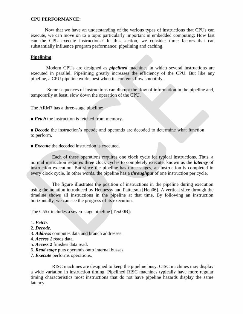
CPU PERFORMANCE:
Now that we have an understanding of the various types of instructions that CPUs can
execute, we can move on to a topic particularly important in embedded computing: How fast
can the CPU execute instructions? In this section, we consider three factors that can substantially influence program performance: pipelining and caching.
Pipelining
Modern CPUs are designed as pipelined machines in which several instructions are
executed in parallel. Pipelining greatly increases the efficiency of the CPU. But like any
pipeline, a CPU pipeline works best when its contents flow smoothly.
Some sequences of instructions can disrupt the flow of information in the pipeline and,
temporarily at least, slow down the operation of the CPU.
The ARM7 has a three-stage pipeline:
■ Fetch the instruction is fetched from memory.
■ Decode the instruction’s opcode and operands are decoded to determine what function to perform.
■ Execute the decoded instruction is executed.
Each of these operations requires one clock cycle for typical instructions. Thus, a
normal instruction requires three clock cycles to completely execute, known as the latency of instruction execution. But since the pipeline has three stages, an instruction is completed in
every clock cycle. In other words, the pipeline has a throughput of one instruction per cycle.
The figure illustrates the position of instructions in the pipeline during execution
using the notation introduced by Hennessy and Patterson [Hen06]. A vertical slice through the timeline shows all instructions in the pipeline at that time. By following an instruction
horizontally, we can see the progress of its execution.
The C55x includes a seven-stage pipeline [Tex00B]:
1. Fetch.
2. Decode.
3. Address computes data and branch addresses.
4. Access 1 reads data.
5. Access 2 finishes data read.
6. Read stage puts operands onto internal busses.
7. Execute performs operations.
RISC machines are designed to keep the pipeline busy. CISC machines may display
a wide variation in instruction timing. Pipelined RISC machines typically have more regular timing characteristics most instructions that do not have pipeline hazards display the same
latency.

Caching
We have already discussed caches functionally. Although caches are invisible in the
programming model, they have a profound effect on performance. We introduce caches because they substantially reduce memory access time when the requested location is in the
cache. However, the desired location is not always in the cache since it is considerably
smaller than main memory. As a result, caches cause the time required to access memory to vary considerably. The extra time required to access a memory location not in the cache is
often called the cache miss penalty.
The amount of variation depends on several factors in the system architecture, but a
cache miss is often several clock cycles slower than a cache hit. The time required to access a memory location depends on whether the requested location is in the cache. However, as we have seen, a location may not be in the cache for several reasons.
■ At a compulsory miss, the location has not been referenced before.
■ At a conflict miss, two particular memory locations are fighting for the same cache line. ■ At a capacity miss, the program’s working set is simply too large for the cache.
The contents of the cache can change considerably over the course of execution of a program. When we have several programs running concurrently on the CPU,
CPU POWER CONSUMPTION:
Power consumption is, in some situations, as important as execution time. In this
section we study the characteristics of CPUs that influence power consumption and
mechanisms provided by CPUs to control how much power they consume.
First, it is important to distinguish between energy and power. Power is, of course,
energy consumption per unit time. Heat generation depends on power consumption. Battery
life, on the other hand, most directly depends on energy consumption. Generally, we will use
the term power as shorthand for energy and power consumption, distinguishing between them
only when necessary.
The high-level power consumption characteristics of CPUs and other system
components are derived from the circuits used to build those components. Today, virtually all
digital systems are built with complementary metal oxide semiconductor (CMOS) circuitry.
The detailed circuit characteristics are best left to a study of VLSI design [Wol08], but the
basic sources of CMOS power consumption are easily identified and briefly described below. ■ Voltage drops: The dynamic power consumption of a CMOS circuit is proportional to the square of the power supply voltage (V
2). Therefore, by reducing the power supply voltage to
the lowest level that provides the required performance, we can significantly reduce power consumption. We also may be able to add parallel hardware and even further reduce the power supply voltage while maintaining required performance.
■ Toggling: A CMOS circuit uses most of its power when it is changing its output value. This
provides two ways to reduce power consumption. By reducing the speed at which the circuit
operates, we can reduce its power consumption (although not the total energy required for the
operation, since the result is available later).We can actually reduce energy consumption by
eliminating unnecessary changes to the inputs of a CMOS circuit—eliminating unnecessary
glitches at the circuit outputs eliminates unnecessary power consumption.
UNIT II EMBEDDED COMPUTING PLATFORM DESIGN 9 The CPU Bus-Memory
devices and systems–Designing with computing platforms – consumer electronics
architecture – platform-level performance analysis - Components for embedded programs-
Models of programs- Assembly, linking and loading – compilation techniques- Program level
performance analysis – Software performance optimization – Program level energy and
power analysis and optimization – Analysis and optimization of program size- Program
validation and testing.

UNIT II
COMPUTING PLATFORM AND DESIGN ANALYSIS
CPU BUSES:
A computer system encompasses much more than the CPU;it also includes memory and I/O
devices. The bus is the mechanism by which the CPU communicates with memory and devices. A bus is, at a minimum, a collection of wires, but the bus also defines a protocol by which the CPU, memory,
and devices communicate. One of the major roles of the bus is to provide an interface to memory. (Of course, I/O devices also connect to the bus.)
Bus Protocols:
The basic building block of most the
figure. The handshake ensures that transmit and the other is ready to receive.
bus protocols is the four-cycle handshake, illustrated in
when two devices want to communicate, one is ready to
The handshake uses a pair of wires dedicated to the handshake: enq (meaning enquiry) and ack
(meaning acknowledge). Extra wires are used for the data transmitted during the handshake. The four
cycles are described below.
1. Device 1 raises its output to signal an enquiry, which tells device 2 that it should get ready to listen for data.
2. When device 2 is ready to receive, it raises its output to signal an acknowledgment. At this point, devices 1 and 2 can transmit or receive.
3. Once the data transfer is complete, device 2 lowers its output, signaling that it has received the data.
4. After seeing that ack has been released, device 1 lowers its output.
At the end of the handshake, both handshaking signals are low, just as they were at the start of the
handshake. The system has thus returned to its original state in readiness for another handshake-enabled data transfer.
Microprocessor buses build on the handshake for communication between the CPU and other system components. The term bus is used in two ways.
The most basic use is as a set of related wires, such as address wires. However, the term may also
mean a protocol for communicating between components.
To avoid confusion, we will use the term bundle to refer to a set of related signals. The
fundamental bus operations are reading and writing. The figure shows the structure of a typical bus that
supports reads and writes.
The major components follow:
■ Clock provides synchronization to the bus components,
■ R/W is true when the bus is reading and false when the bus is writing,
■ Address is an a-bit bundle of signals that transmits the address for an access,
■ Data is an n-bit bundle of signals that can carry data to or from the CPU, and
■ Data ready signals when the values on the data bundle are valid. DMA:
Standard bus transactions require the CPU to be in the middle of every read and write transaction. However, there are certain types of data transfers in which the CPU does not need to be involved.
For example, a high-speed I/O device may want to transfer a block of data into memory. While it is possible to write a program that alternately reads the device and writes to memory, it would be faster to eliminate the CPU’s involvement and let the device and memory communicate directly. This capability requires that some unit other than the CPU be able to control operations on the bus.
Direct memory access (DMA) is a bus operation that allows reads and writes not controlled by
the CPU. A DMA transfer is controlled by a DMA controller, which requests control of the bus from
the CPU.
After gaining control, the DMA controller performs read and write operations directly between devices and memory. Figure 2.3 shows the configuration of a bus with a DMA controller. The DMA
requires the CPU to provide two additional bus signals:
■ The bus request is an input to the CPU through which DMA controllers
ask for ownership of the bus.
■ The bus grant signals that the bus has been granted to the DMA controller.
A device that can initiate its own bus transfer is known as a bus master. Devices that do not have
the capability to be bus masters do not need to connect to a bus request and bus grant.
The DMA controller uses these two signals to gain control of the bus using a classic four-cycle handshake. The bus request is asserted by the DMA controller when it control the bus, and the bus grant
is asserted by the CPU when the bus is ready.
The CPU will finish all pending bus transactions before granting control of the bus to the DMA controller. When it does grant control, it stops driving the other bus signals: R/W, address, and so on.
Upon becoming bus master, the DMA controller has control of all bus signals (except, of course, for bus request and bus grant).
MEMORY DEVICES: There are several varieties of both read-only and read/write memories, each with its own
advantages. After discussing some basic characteristics of memories, we describe RAMs and then ROMs.
Memory Device Organization: The most basic way to characterize a memory is by its capacity, such as 256 MB. However,
manufacturers usually make several versions of a memory of a given size, each with a different data width. For example, a 256-MB memory may be available in two versions: ■ As a 64M *4-bit array, a single memory access obtains an 8-bit data item, with a maximum of 2
26
different addresses. ■ As a 32 M* 8-bit array, a single memory access obtains a 1-bit data item, with a maximum of 2
23
different addresses.
The height/width ratio of a memory is known as its aspect ratio. The best aspect ratio depends on
the amount of memory required. Internally, the data are stored in a two-dimensional array of memory
cells as shown in Figure 2.4. Because the array is stored in two dimensions, the n-bit address received
by the chip is split into a row and a column address (with n =r+ c).
The row and column select a particular memory cell. If the memory’s external width is 1 bit, the
column address selects a single bit; for wider data widths, the column address can be used to select a
subset of the columns. Most memories include an enable signal that controls the tri-stating of data onto
the memory’s pins.
Random-Access Memories:
o Random-access memories can be both read and written. They are called random access because,
unlike magnetic disks, addresses can be read in any order. Most bulk memory in modern systems is dynamic RAM (DRAM). DRAM is very dense; it does, however, require that its values be refreshed periodically since the values inside the memory cells decay over time.
o The dominant form of dynamic RAM today is the synchronous DRAMs (SDRAMs), which
uses clocks to improve DRAM performance. SDRAMs use Row Address Select (RAS) and Column Address Select (CAS) signals to break the address into two parts, which select the proper row and column in the RAM array. Signal transitions are relative to the SDRAM clock,which allows the internal SDRAM operations to be pipelined.
The transitions on the control signals are related to a clock [Mic00]. RAS_ and CAS_ can therefore become valid at the same time.
o The address lines are not shown in full detail here; some address lines may not be active depending on the mode in use. SDRAMs use a separate refresh signal to control refreshing. DRAM has to be refreshed roughly once per millisecond.
o Rather than refresh the entire memory at once, DRAMs refresh part of the memory at a time.
When a section of memory is being refreshed, it cannot be accessed until the refresh is complete. The memory refresh occurs over fairly few seconds so that each section is refreshed every few microseconds.
o SDRAMs include registers that control the mode in which the SDRAM operates. SDRAMs
support burst modes that allow several sequential addresses to be accessed by sending only one address. SDRAMs generally also support an interleaved mode that exchanges pairs of bytes.
Read-Only Memories:
o Read-only memories (ROMs) are preprogrammed with fixed data. They are very useful in
embedded systems since a great deal of the code, and perhaps some data, does not change over time. Read-only memories are also less sensitive to radiation induced errors.
o There are several varieties of ROM available. The first-level distinction to be made is between
factory-programmed ROM (sometimes called mask-programmed ROM) and field-programmable ROM.
o Factory-programmed ROMs are ordered from the factory with particular programming. ROMs can typically be ordered in lots of a few thousand, but clearly factory programming is useful only when the ROMs are to be installed in some quantity.
o Field-programmable ROMs, on the other hand, can be programmed in the lab. Flash memory is
the dominant form of field-programmable ROM and is electrically erasable.
o Flash memory uses standard system voltage for erasing and programming, allowing it to be reprogrammed inside a typical system. This allows applications such as automatic distribution of upgrades—the flash memory can be reprogrammed while downloading the new memory contents from a telephone line.
o Early flash memories had to be erased in their entirety; modern devices allow memory to be
erased in blocks. Most flash memories today allow certain blocks to be protected.
o A common application is to keep the boot-up code in a protected block but allow updates to other memory blocks on the device. As a result, this form of flash is commonly known as boot-block flash.

I/O DEVICES:
Some of these devices are often found as on-chip devices in micro-controllers; others are generally implemented separately but are still commonly used. Looking at a few important devices now will help us understand both the requirements of device interfacing.
Timers and Counters:
Timers and counters are distinguished from one another largely by their use, not their logic. Both are built from adder logic with registers to hold the current value, with an increment input that adds one to the current register value.
However, a timer has its count connected to a periodic clock signal to measure time intervals, while a counter has its count input connected to an aperiodic signal in order to count the number of occurrences of some external event. Because the same logic can be used for either purpose, the device is often called a counter/timer.
Figure 2.6 shows enough of the internals of a counter/timer to illustrate its operation. An n-bit counter/timer uses an n-bit register to store the current state of the count and an array of half subtractors to decrement the count when the count signal is asserted.
Combinational logic checks when the count equals zero; the done output signals the zero
count. It is often useful to be able to control the time-out, rather than require exactly 2n
events to occur. For this purpose, a reset register provides the value with which the count
register is to be loaded.
The counter/timer provides logic to load the reset register. Most counters provide both cyclic and acyclic modes of operation. In the cyclic mode, once the counter reaches the done state, it is automatically reloaded and the counting process continues. In acyclic mode, the counter/timer waits for an explicit signal from the microprocessor to resume counting.
A watchdog timer is an I/O device that is used for internal operation of a system. As
shown in Figure 2.7, the watchdog timer is connected into the CPU bus and also to the
CPU’s reset line.
The CPU’s software is designed to periodically reset the watchdog timer, before the
timer ever reaches its time-out limit. If the watchdog timer ever does reach that limit, its
time-out action is to reset the processor. In that case, the presumption is that either a
software flaw or hardware problem has caused the CPU to misbehave. Rather than
diagnose the problem, the system is reset to get it operational as quickly as possible.
A/D and D/A Converters
Analog/digital (A/D) and digital/analog (D/A) converters (typically known as ADCs and DACs, respectively) are often used to interface non digital devices to embedded systems.
The design of A/D and D/A converters themselves is beyond the scope of this book; we concentrate instead on the interface to the microprocessor bus. Because A/D conversion requires more complex circuitry, it requires a somewhat more complex interface.
Analog/digital conversion requires sampling the analog input before converting it to digital form. A control signal causes the A/D converter to take a sample and digitize it.
There are several different types of A/D converter circuits, some of which take a constant
amount of time, while the conversion time of others depends on the sampled value. Variable-time converters provide a done signal so that the microprocessor knows when the value is ready.
A typical A/D interface has, in addition to its analog inputs, two major digital inputs. A data port allows A/D registers to be read and written, and a clock input tells when to start the next conversion.
D/A conversion is relatively simple, so the D/A converter interface generally includes only the data value. The input value is continuously converted to analog form.
LEDs
Light-emitting diodes (LEDs) are often used as simple displays by themselves, and arrays of LEDs may form the basis of more complex displays. Figure 2.8 shows how to connect an LED to a digital output.
A resistor is connected between the output pin and the LED to absorb the voltage difference between the digital output voltage and the 0.7 V drop across the LED. When the digital output goes to 0, the LED voltage is in the devices off region and the LED is not on.
Displays
A display device may be either directly driven or driven from a frame buffer. Typically, displays with a small number of elements are driven directly by logic, while large displays use a RAM frame buffer.
The n-digit array, shown in Figure 2.9, is a simple example of a display that is usually directly driven. A single-digit display typically consists of seven segments; each segment may be either an LED or a liquid crystal display (LCD) element.
Display relies on the digits being visible for some time after the drive to the digit is removed,
which is true for both LEDs and LCDs.
The digit input is used to choose which digit is currently being updated, and the selected digit activates its display elements based on the current data value.
The display’s driver is responsible for repeatedly scanning through the digits and presenting the
current value of each to the display.
A frame buffer is a RAM that is attached to the system bus. The microprocessor writes values
into the frame buffer in whatever order is desired.
The pixels in the frame buffer are generally written to the display in raster order (by tradition, the screen is in the fourth quadrant) by reading pixels sequentially.
Many large displays are built using LCD. Each pixel in the display is formed by a single liquid crystal.
Early LCD panels were called passive matrix because they relied on a two-dimensional grid of wires to address the pixels. Modern LCD panels use an active matrix system that puts a transistor at each pixel to control access to the LCD. Active matrix displays provide higher contrast and a higher-quality display.
Touchscreens
A touchscreen is an input device overlaid on an output device. The touchscreen registers the position of a touch to its surface. By overlaying this on a display, the user can react to information shown on the display.
The two most common types of touchscreens are resistive and capacitive. A resistive touchscreen uses a two-dimensional voltmeter to sense position. As shown in Figure 2.10, the touchscreen consists of two conductive sheets separated by spacer balls. The top conductive sheet is flexible so that it can be pressed to touch the bottom sheet.
A voltage is applied across the sheet; its resistance causes a voltage gradient to appear across the sheet. The top sheet samples the conductive sheet’s applied voltage at the contact point. An analog/digital converter is used to measure the voltage and resulting position.
The touchscreen alternates between x and y position sensing by alternately applying horizontal and vertical voltage gradients information shown on the display.
The two most common types of touchscreens are resistive and capacitive. A resistive touchscreen uses a two-dimensional voltmeter to sense position. As shown in Figure 2.10, the touchscreen consists of two conductive sheets separated by spacer balls. The top conductive sheet is flexible so that it can be pressed to touch the bottom sheet.
A voltage is applied across the sheet; its resistance causes a voltage gradient to appear across the
sheet. The top sheet samples the conductive sheet’s applied voltage at the contact point. An analog/digital converter is used to measure the voltage and resulting position.
The touchscreen alternates between x and y position sensing by alternately applying horizontal and vertical voltage gradients.

COMPONENT INTERFACING:
Building the logic to interface a device to a bus is not too difficult but does take some attention to
detail. We first consider interfacing memory components to the bus, since that is relatively simple, and then use those concepts to interface to other types of devices.
Memory Interfacing If we can buy a memory of the exact size we need, then the memory structure is simple. If we
need more memory than we can buy in a single chip, then we must construct the memory out of several chips. We may also want to build a memory that is wider than we can buy on a single chip; for example, we cannot generally buy a 32-bit-wide memory chip. We can
wwe
wa
.as
ninlay
unic
veo
rzn
its
y.tcrou
mct a memory
of a given width (32 bits, 64 bits, etc.) by placing RAMs in parallel.
We also need logic to turn the bus signals into the appropriate memory signals. For example, most
busses won’t send address signals in row and column form. We also need to generate the appropriate refresh signals.
Device Interfacing
Some I/O devices are designed to interface directly to a particular bus, forming glueless
interfaces. But glue logic is required when a device is connected to a bus for which it is not designed.
An I/O device typically requires a much smaller range of addresses than a memory, so
addresses must be decoded much more finely. Some additional logic is required to cause the bus to read
and write the device’s registers.
DESIGN WITH MICROPROCESSORS:
System Architecture
We know that an architecture is a set of elements and the relationships between them that
together form a single unit. The architecture of an embedded computing system is the blueprint for implementing that system—it tells you what components you need and how you put them together.
The architecture of an embedded computing system includes both hardware and software
elements. Let’s consider each in turn.
The hardware architecture of an embedded computing system is the more obvious manifestation of the architecture since you can touch it and feel it. It includes several elements, some of which may be less obvious than others.
o CPU An embedded computing system clearly contains a microprocessor. But which one? There are many different architectures, and even within an architecture we can select between models that vary in clock speed, bus data width, integrated peripherals, and so on. The choice of the
CPU is one of the most important, but it cannot be made without considering the software that will execute on the machine.
o Bus The choice of a bus is closely tied to that of a CPU, since the bus is an integral part of the
microprocessor. But in applications that make intensive use of the bus due to I/O or other data traffic, the bus may be more of a limiting factor than the CPU. Attention must be paid to the required data bandwidths to be sure that the bus can handle the traffic.
o Memory Once again, the question is not whether the system will have memory but the
characteristics of that memory. The most obvious characteristic is total size, which depends on
both the required data volume and the size of the program instructions. The ratio of ROM to
RAM and selection of DRAM versus SRAM can have a significant influence on the cost of the
system. The speed of the memory will play a large part in determining system performance.
o Input and output devices The user’s view of the input and output mechanisms may not
correspond to the devices connected to the microprocessor. For example, a set of switches and
knobs on a front panel may all be controlled by a single microcontroller, which is in turn
connected to the main CPU.
For a given function, there may be several different devices of varying sophistication and cost that can do the job. The difficulty of using a particular device, such as the amount of glue logic required to interface it, may also play a role in final device selection.
Hardware Design
The design complexity of the hardware platform can vary greatly, from a totally off-the-shelf
solution to a highly customized design. At the board level, the first step is to consider evaluation boards supplied by the microprocessor
manufacturer or another company working in collaboration with the manufacturer. Evaluation boards
are sold for many microprocessor systems; they typically include the CPU, some memory, a serial link
for downloading programs, and some minimal number of I/O devices. Figure 2.11 shows an ARM
evaluation board manufactured by Sharp.
The evaluation board may be a complete solution or provide what you need with only slight
modifications. If the evaluation board is supplied by the microprocessor vendor, its design (netlist,
board layout, etc.) may be available from the vendor; companies provide such information to make it
easy for customers to use their microprocessors. If the evaluation board comes from a third party, it may
be possible to contract them to design a new board with your required modifications, or you can start
from scratch on a new board design.
The other major task is the choice of memory and peripheral components. In the case of I/O
devices, there are two alternatives for each device: selecting a component from a catalog or designing one yourself. When shopping for devices from a catalog, it is important to read data sheets carefully it
may not be trivial to figure out whether the device does what you need it to do.
DEVELOPMENT AND DEBUGGING:
Development Environments
A typical embedded computing system has a relatively small amount of everything, including
CPU horsepower, memory, I/O devices, and so forth. As a result, it is common to do at least part of the
software development on a PC or workstation known as a host as illustrated in Figure 2.12. The
hardware on which the code will finally run is known as the target. The host and target are frequently
connected by a USB link, but a higher-speed link such as Ethernet can also be used.
The target must include a small amount of software to talk to the host system. That software will
take up some memory, interrupt vectors, and so on, but it should generally leave the smallest possible
footprint in the target to avoid interfering with the application software.
The host should be able to do the following:
■ load programs into the target,
■ start and stop program execution on the target, and
■ examine memory and CPU registers.
Debugging Techniques: A good deal of software debugging can be done by compiling and executing the code on a PC or
workstation. But at some point it inevitably becomes necessary to run code on the embedded hardware platform.
Embedded systems are usually less friendly programming environments than PCs. Nonetheless, the resourceful designer has several options available for debugging the system.
The serial port found on most evaluation boards is one of the most important debugging tools. In fact, it is often a good idea to design a serial port into an embedded system even if it will not be used in the final product; the serial port can be used not only for development debugging but also for diagnosing problems in the field.
Another very important debugging tool is the breakpoint. The simplest form of a breakpoint is for the user to specify an address at which the program’s execution is to break. When the PC reaches that address, control is returned to the monitor program. From the monitor program, the user can examine and/or modify CPU registers, after which execution can be continued. Implementing breakpoints does not require using exceptions or external devices.
Debugging Challenges
Logical errors in software can be hard to track down, but errors in real-time code can create problems that are even harder to diagnose. Real-time programs are required to finish their work within a certain amount of time; if they run too long, they can create very unexpected behavior.
The exact results of missing real-time deadlines depend on the detailed characteristics of the I/O devices and the nature of the timing violation. This makes debugging real-time problems especially difficult.
Unfortunately, the best advice is that if a system exhibits truly unusual behavior, missed deadlines should be suspected. In-circuit emulators, logic analyzers, and even LEDs can be useful tools in checking the execution time of real-time code to determine whether it in fact meets its deadline.
PROGRAM DESIGN:
Components for Embedded Programs:
In this section, we consider code for three structures or components that are commonly used in
embedded software: the state machine, the circular buffer, and the queue. State machines are well suited to reactive systems such as user interfaces; circular buffers and queues are useful in digital signal processing.
State Machines
When inputs appear intermittently rather than as periodic samples, it is often convenient to think
of the system as reacting to those inputs.
The reaction of most systems can be characterized in terms of the input received and the current state of the system. This leads naturally to a finite-state machine style of describing the reactive
system’s behavior.
Moreover, if the behavior is specified in that way, it is natural to write the program implementing that behavior in a state machine style.
The state machine style of programming is also an efficient implementation of such computations. Finite-state machines are usually first encountered in the context of hardware design.
Stream-Oriented Programming and Circular Buffers
The data stream style makes sense for data that comes in regularly and must be processed on the
fly. For each sample, the filter must emit one output that depends on the values of the last n inputs. In a
typical workstation application, we would process the samples over a given interval by reading them all
in from a file and then computing the results all at once in a batch process. In an embedded system we
must not only emit outputs in real time, but we must also do so using a minimum amount of memory.
The circular buffer is a data structure that lets us handle streaming data in an efficient way.
The figure illustrates how a circular buffer stores a subset of the data stream. At each point in time, the
algorithm needs a subset of the data stream that forms a window into the stream. The window slides
with time as we throw out old values no longer needed and add new values. Since the size of the
window does not change, we can use a fixed-size buffer to hold the current data.
To avoid constantly copying data within the buffer, we will move the head of the buffer in
time. The buffer points to the location at which the next sample will be placed; every time we add a
sample, we automatically overwrite the oldest sample, which is the one that needs to be thrown out. When the pointer gets to the end of the buffer, it wraps around to the top.
MODELS OF PROGRAMS:
Data Flow Graphs:
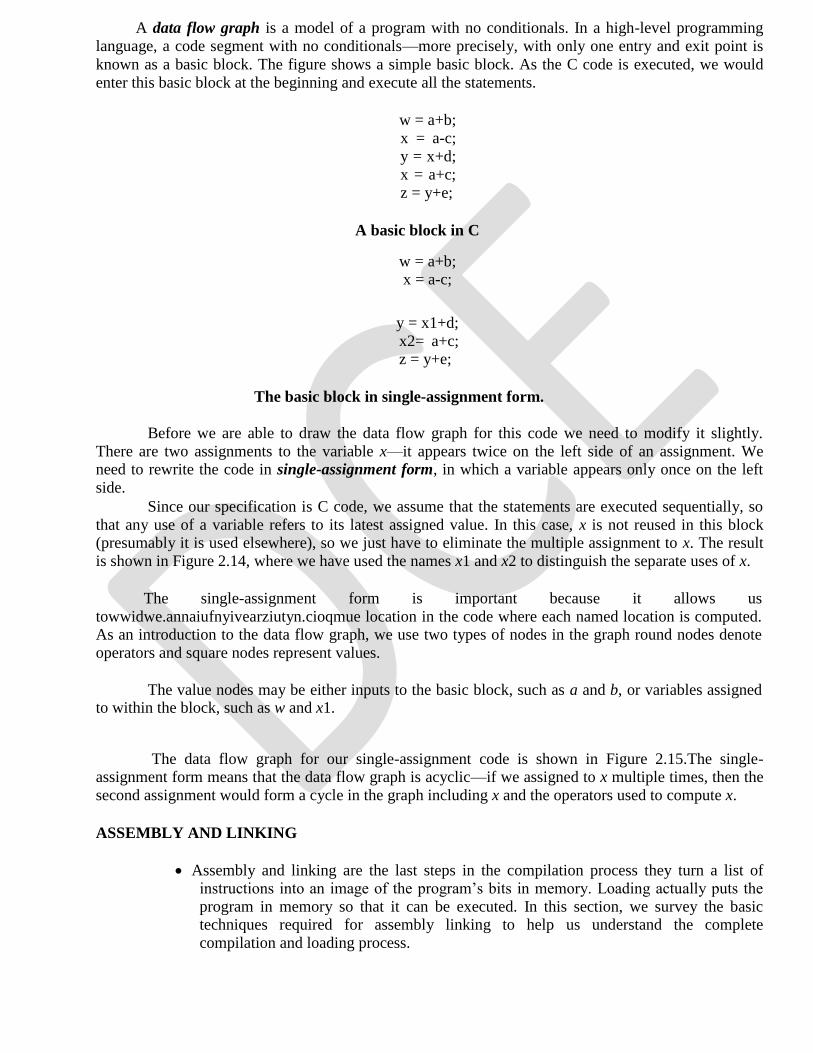
A data flow graph is a model of a program with no conditionals. In a high-level programming
language, a code segment with no conditionals—more precisely, with only one entry and exit point is
known as a basic block. The figure shows a simple basic block. As the C code is executed, we would
enter this basic block at the beginning and execute all the statements.
w = a+b;
x = a-c;
y = x+d;
x = a+c;
z = y+e;
A basic block in C
w = a+b; x = a-c;
y = x1+d;
x2= a+c; z = y+e;
The basic block in single-assignment form.
Before we are able to draw the data flow graph for this code we need to modify it slightly.
There are two assignments to the variable x—it appears twice on the left side of an assignment. We need to rewrite the code in single-assignment form, in which a variable appears only once on the left
side. Since our specification is C code, we assume that the statements are executed sequentially, so
that any use of a variable refers to its latest assigned value. In this case, x is not reused in this block (presumably it is used elsewhere), so we just have to eliminate the multiple assignment to x. The result
is shown in Figure 2.14, where we have used the names x1 and x2 to distinguish the separate uses of x.
The single-assignment form is important because it allows us
towwidwe.annaiufnyivearziutyn.cioqmue location in the code where each named location is computed. As an introduction to the data flow graph, we use two types of nodes in the graph round nodes denote
operators and square nodes represent values.
The value nodes may be either inputs to the basic block, such as a and b, or variables assigned
to within the block, such as w and x1.
The data flow graph for our single-assignment code is shown in Figure 2.15.The single-assignment form means that the data flow graph is acyclic—if we assigned to x multiple times, then the
second assignment would form a cycle in the graph including x and the operators used to compute x.
ASSEMBLY AND LINKING
Assembly and linking are the last steps in the compilation process they turn a list of instructions into an image of the program’s bits in memory. Loading actually puts the
program in memory so that it can be executed. In this section, we survey the basic techniques required for assembly linking to help us understand the complete
compilation and loading process.
The figure highlights the role of assemblers and linkers in the compilation process. This
process is often hidden from us by compilation commands that do everything required
to generate an executable program. As the figure shows, most compilers do not directly
generate machine code, but instead create the instruction-level program in the form of
human-readable assembly language. Generating assembly language rather than binary
instructions frees the compiler writer from details extraneous to the compilation
process, which includes the instruction format as well as the exact addresses of
instructions and data.
The assembler’s job is to translate symbolic assembly language statements into bit-level
representations of instructions known as object code. The assembler takes care of
instruction formats and does part of the job of translating labels into addresses.
However, since the program may be built from many files, the final steps in
determining the addresses of instructions and data are performed by the linker, which
produces an executable binary file. That file may not necessarily be located in the
CPU’s memory, however, unless the linker happens to create the executable directly in
RAM. The program that brings the program into memory for execution is called a
loader.
The simplest form of the assembler assumes that the starting address of the assembly language program has been specified by the programmer. The addresses in such a
program are known as absolute addresses.
Assemblers
When translating assembly code into object code, the assembler must translate opcodes and format
the bits in each instruction, and translate labels into addresses. In this section, we review the translation
of assembly language into binary. Labels make the assembly process more complex, but they are the
most important abstraction provided by the assembler. Labels let the programmer (a human programmer
or a compiler generating assembly code) avoid worrying about the locations of instructions and data.
Label processing requires making two passes through the assembly source code as follows:
1. The first pass scans the code to determine the address of each label.
2. The second pass assembles the instructions using the label values computed in the first pass.
As shown in Figure 2.17, the name of each symbol and its address is stored in a symbol table
www.annauniverzity.com that is built during the first pass. The symbol table is built by scanning from th first instruction to the last.
During scanning, the current location in memory is kept in a program location counter (PLC).
Despite the similarity in name to a program counter, the PLC is not used to execute the program, only to
assign memory locations to labels. For example, the PLC always makes exactly one pass through the
program, whereas the program counter makes many passes over code in a loop. Thus, at the start of the
first pass, the PLC is set to the program’s starting address and the assembler looks at the first line. After
examining the line, the assembler updates the PLC to the next location (since ARM instructions are four
bytes long, the PLC would be incremented by four) and looks at the next instruction. If the instruction
begins with a label, a new entry is made in the symbol table, which includes the label name and its
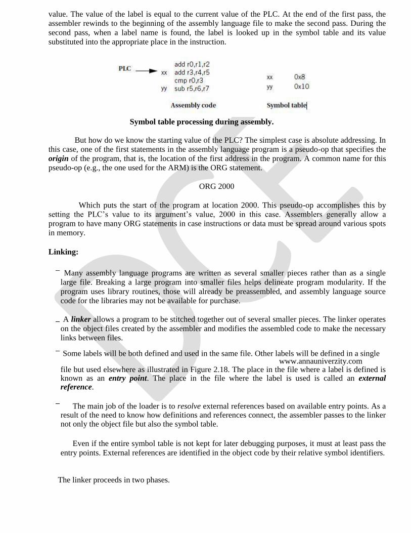
value. The value of the label is equal to the current value of the PLC. At the end of the first pass, the
assembler rewinds to the beginning of the assembly language file to make the second pass. During the
second pass, when a label name is found, the label is looked up in the symbol table and its value
substituted into the appropriate place in the instruction.
Symbol table processing during assembly.
But how do we know the starting value of the PLC? The simplest case is absolute addressing. In
this case, one of the first statements in the assembly language program is a pseudo-op that specifies the
origin of the program, that is, the location of the first address in the program. A common name for this
pseudo-op (e.g., the one used for the ARM) is the ORG statement.
ORG 2000
Which puts the start of the program at location 2000. This pseudo-op accomplishes this by
setting the PLC’s value to its argument’s value, 2000 in this case. Assemblers generally allow a
program to have many ORG statements in case instructions or data must be spread around various spots
in memory.
Linking:
Many assembly language programs are written as several smaller pieces rather than as a single
large file. Breaking a large program into smaller files helps delineate program modularity. If the
program uses library routines, those will already be preassembled, and assembly language source
code for the libraries may not be available for purchase.
A linker allows a program to be stitched together out of several smaller pieces. The linker operates
on the object files created by the assembler and modifies the assembled code to make the necessary
links between files.
Some labels will be both defined and used in the same file. Other labels will be defined in a single www.annauniverzity.com
file but used elsewhere as illustrated in Figure 2.18. The place in the file where a label is defined is known as an entry point. The place in the file where the label is used is called an external reference.
The main job of the loader is to resolve external references based on available entry points. As a result of the need to know how definitions and references connect, the assembler passes to the linker not only the object file but also the symbol table.
Even if the entire symbol table is not kept for later debugging purposes, it must at least pass the
entry points. External references are identified in the object code by their relative symbol identifiers.
The linker proceeds in two phases.
o First, it determines the address of the start of each object file. The order in which object files are
to be loaded is given by the user, either by specifying parameters when the loader is run or by creating a load map file that gives the order in which files are to be placed in memory. Given the order in which files are to be placed in memory and the length of each object file, it is easy to compute the starting address of each file.
o At the start of the second phase, the loader merges all symbol tables from the object files into a single, large table. It then edits the object files to change relative addresses into addresses. This is typically performed by having the assembler write extra bits into the object file to identify the instructions and fields that refer to labels. If a label cannot be found in the merged symbol table, it is undefined and an error message is sent to the user.
BASIC COMPILATION TECHNIQUES:
It is useful to understand how a high-level language program is translated into instructions.
Since implementing an embedded computing system often requires controlling the instruction
sequences used to handle interrupts, placement of data and instructions in memory, and so forth, understanding how the compiler works can help you know when you cannot rely on the compiler.
Next, because many applications are also performance sensitive, understanding how code is generated can help you meet your performance goals, either by writing high-level code that gets
compiled into the instructions you want or by recognizing when you must write your own assembly code.
The compilation process is summarized in Figure 2.19. Compilation begins with high-level
language code such as C and generally produces assembly code. (Directly producing object code simply duplicates the functions of an assembler which is a very desirable stand-alone program to have.)
The high-level language program is parsed to break it into statements and expressions. In
addition, a symbol table is generated, which includes all the named objects in the program. Some
compilers may then perform higher-level optimizations that can be viewed as modifying the high-level language program input without reference to instructions.
Simplifying arithmetic expressions is one example of a machine-independent optimization. Not
all compilers do such optimizations, and compilers can vary widely regarding which combinations of
machine-independent optimizations they do perform.
Instruction-level optimizations are aimed at generating code. They may work directly on real
instructions or on a pseudo-instruction format that is later mapped onto the instructions of the target
CPU. This level of optimization also helps modularize the compiler by allowing code generation to create simpler code that is later optimized. For example, consider the following array access code:
x[i] = c*x[i]; A simple code generator would generate the address for x[i] twice, once
for each appearance in the statement. The later optimization phases can recognize this as an
example of common expressions that need not be duplicated. While in this simple case it would be possible to create a code generator that never generated the redundant expression,
taking into account every such optimization at code generation time is very difficult. We get better code and more reliable compilers by generating simple code first and then optimizing it.
ANALYSIS AND OPTIMIZATION OF EXCUTION TIME, POWER, ENERGY , PROGRAM
SIZE:
The memory footprint of a program is determined by the size of its data and instructions. Both
must be considered to minimize program size.
Data provide an excellent opportunity for minimizing size because the data are most highly dependent on programming style. Because inefficient programs often keep several copies of data, identifying and eliminating duplications can lead to significant memory savings usually with little performance penalty.
Buffers should be sized carefully rather than defining a data array to a large size that the program will never attain, determine the actual maximum amount of data held in the buffer and allocate the array accordingly. Data can sometimes be packed, such as by storing several flags in a single word and extracting them by using bit-level operations.
A very low-level technique for minimizing data is to reuse values. For instance, if several constants happen to have the same value, they can be mapped to the same location. Data buffers can often be reused at several different points in the program. This technique must be used with extreme caution, however, since subsequent versions of the program may not use the same values for the constants.
A more generally applicable technique is to generate data on the fly rather than store it. Of course, the code required to generate the data takes up space in the program, but when complex data structures are involved there may be some net space savings from using code to generate data.
Minimizing the size of the instruction text of a program requires a mix of high-level program
transformations and careful instruction selection.
Encapsulating functions in subroutines can reduce program size when done carefully. Because
subroutines have overhead for parameter passing that is not obvious from the high-level language code, there is a minimum-size function body for which a subroutine makes sense.
www.annauniverzity.com
Architectures that have variable-size instruction lengths are particularly g od candidates for careful coding to minimize program size, which may require assembly language coding of key program segments. There may also be cases in which one or a sequence of instructions is
much smaller than alternative implementations for example, a multiply-accumulate instruction may be both smaller and faster than separate arithmetic operations.
When reducing the number of instructions in a program, one important technique is the proper
use of subroutines. If the program performs identical operations repeatedly, these operations are natural candidates for subroutines.
Even if the operations vary somewhat, you may be able to construct a properly parameterized
subroutine that saves space. Of course, when considering the code size savings, the subroutine
linkage code must be counted into the equation. There is extra code not only in the subroutine
body but also in each call to the subroutine that handles parameters.. In some cases, proper
instruction selection may reduce code size; this is particularly true in CPUs that use variable-length instructions
Some microprocessor architectures support dense instruction sets, specially designed
instruction sets that use shorter instruction formats to encode the instructions.
The ARM Thumb instruction set and the MIPS-16 instruction set for the MIPS architecture are
two examples of this type of instruction set. In many cases, a microprocessor that supports the dense instruction set also supports the normal instruction set, although it is possible to build a microprocessor that executes only the dense instruction set.
Special compilation modes produce the program in terms of the dense instruction set. Program
size of course varies with the type of program, but programs using the dense instruction set are often 70 to 80% of the size of the standard instruction set equivalents.
PROGRAM VALIDATION AND TESTING :
Complex systems need testing to ensure that they work as they are intended. But bugs can be
subtle, particularly in embedded systems, where specialized hardware and real-time responsiveness
make programming more challenging. Fortunately, there are many available techniques for software testing that can help us generate a comprehensive set of tests to ensure that our system works properly.
The first question we must ask ourselves is how much testing is enough. Clearly, we cannot test
the program for every possible combination of inputs. Because we cannot implement an infinite number of tests, we naturally ask ourselves what a reasonable standard of thoroughness is. One of the major
contributions of software testing is to provide us with standards of thoroughness that make sense.
Following these standards does not guarantee that we will find all bugs.
The two major types of testing strategies:
■ Black-box methods generate tests without looking at the internal structure of the program.
■ Clear-box (also known as white-box) methods generate tests based on the program structure.
Clear-Box Testing:
The control/data flow graph extracted from a program’s source code is an important tool in
developing clear-box tests for the program. To adequately test the program, we must exercise both its
control and data operations.
In order to execute and evaluate these tests, we must be able to control variables in the program
and observe the results of computations, much as in manufacturing testing. In general, we may need to
modify the program to make it more testable. By adding new inputs and outputs, we can usually
substantially reduce the effort required to find and execute the test.
No matter what we are testing, we must accomplish the following three things in a test:
■ Provide the program with inputs that exercise the test we are interested in.
■ Execute the program to perform the test.
■ Examine the outputs to determine whether the test was successful.
Black-Box Testing:
Black-box tests are generated without knowledge of the code being tested. When used
alone, black-box tests have a low probability of finding all the bugs in a program. But when
used in conjunction with clear-box tests they help provide a well-rounded test set, since black-
box tests are likely to uncover errors that are unlikely to be found by tests extracted from the
code structure.
Black-box tests can really work. For instance, when asked to test an instrument whose
front panel was run by a microcontroller, one acquaintance of the author used his hand to
depress all the buttons simultaneously. The front panel immediately locked up. This situation
could occur in practice if the instrument were placed face-down on a table, but discovery of
this bug would be very unlikely via clear-box tests.
One important technique is to take tests directly from the specification for the code under design. The specification should state which outputs are expected for certain inputs.
Tests should be created that provide specified outputs and evaluate whether the results also satisfy the inputs.
We can’t test every possible input combination, but some rules of thumb help us
select reasonable sets of inputs. When an input can range across a set of values, it is a very
good idea to test at the ends of the range. For example, if an input must be between 1 and 10, 0,
1, 10, and 11 are all important values to test. We should be sure to consider tests both within
and outside the range, such as, testing values within the range and outside the range. We may
want to consider tests well outside the valid range as well as boundary-condition tests.
Random tests form one category of black-box test. Random values are generated with
a given distribution. The expected values are computed independently of the system, and then
the test inputs are applied. A large number of tests must be applied for the results to be
statistically significant, but the tests are easy to generate. Another scenario is to test certain
types of dwawtwa.avnnauluniveesrz.ityF.comr example, integer valued inputs can be generated
at interesting values such as 0, 1, and values near the maximum end of the data range. Illegal
values can be tested as well.
Regression tests form an extremely important category of tests. When tests are
created during earlier stages in the system design or for previous versions of the system, those
tests should be saved to apply to the later versions of the system. Clearly, unless the system

specification changed, the new system should be able to pass old tests. In some cases old bugs
can creep back into systems, such as when an old version of a software module is inadvertently
installed. In other cases regression tests simply exercise the code in different ways than would
be done for the current version of the code and therefore possibly exercise different bugs.
UNIT III
PROCESS AND OPERATING SYSTEMS
MULTIPLE TASKS AND MULTIPLE PROCESSES:
Tasks and Processes
Many (if not most) embedded computing systems do more than one thing that is, the
environment can cause mode changes that in turn cause the embedded system to behave quite differently. For example, when designing a telephone answering machine,
We can define recording a phone call and operating the user’s control panel as distinct tasks,
because they perform logically distinct operations and they must be performed at very different
rates. These different tasks are part of the system’s functionality, but that application-level
organization of functionality is often reflected in the structure of the program as well.
A process is a single execution of a program. If we run the same program two different times,
we have created two different processes. Each process has its own state that includes not only its
registers but all of its memory. In some OSs, the memory management unit is used to keep each
process in a separate address space. In others, particularly lightweight RTOSs, the processes run
in the same address space. Processes that share the same address space are often called threads.
As shown in Figure , this device is connected to serial ports on both ends. The input to the box is an uncompressed stream of bytes. The box emits a compressed string of bits on the output serial line, based on a predefined compression table. Such a box may be used, for example, to compress data being sent to a modem.
The program’s need to receive and send data at different rates for example, the program may
emit 2 bits for the first byte and then 7 bits for the
secondwwbwy.atnenauwnivielrlzitoy.bcovmiously find itself reflected in the structure of the
code. It is easy to create irregular, ungainly code to solve this problem; a more elegant solution
is to create a queue of output bits, with those bits being removed from the queue and sent to the
serial port in 8-bit sets.
But beyond the need to create a clean data structure that simplifies the control structure of the code, we must also ensure that we process the inputs and outputs at the proper rates. For example, if we spend too much time in packaging and emitting output characters, we may drop an input character. Solving timing problems is a more challenging problem.
The text compression box provides a simple example of rate control problems. A control panel on a machine provides an example of a different type of rate control problem, the asynchronous input.
The control panel of the compression box may, for example, include a compression mode button
that disables or enables compression, so that the input text is passed through unchanged when compression is disabled. We certainly do not know when the user will push the compression mode button the button may be depressed asynchronously relative to the arrival of characters for compression.
Multirate Systems
Implementing code that satisfies timing requirements is even more complex when multiple
rates of computation must be handled. Multirate embedded computing systems are very common, including automobile engines, printers, and cell phones. In all these systems, certain operations must be
executed periodically, and each operation is executed at its own rate.
Timing Requirements on Processes
o Processes can have several different types of timing requirements imposed on them by the
application. The timing requirements on a set of processes strongly influence the type of scheduling that is appropriate. A scheduling policy must define the timing requirements that it uses to determine whether a schedule is valid. Before studying scheduling proper, we outline the types of process timing requirements that are useful in embedded system design.
o Figure 3.2 illustrates different ways in which we can define two important requirements on
processes: release time and deadline.
o The release time is the time at which the process becomes ready to execute; this is not necessarily the time at which it actually takes control of the CPU and starts to run. An aperiodic process is by definition initiated by an event, such as external data arriving or data computed by another process.
o The release time is generally measured from that event, although the system may want to make the
process ready at some interval after the event itself. For a periodically executed process, there are two common possibilities.
o In simpler systems, the process may become ready at the beginning of the period. More
sophisticated systems, such as those with data dependencies between processes, may set the release time at the arrival time of certain data, at a time after the start of the period.
o A deadline specifies when a computation must be finished. The deadline for an aperiodic process
is generally measured from the release time, since that is the only reasonable time reference. The deadline for a periodic process may in general occur at some time other than the end of the period.
o Rate requirements are also fairly common. A rate requirement
wsp
wwe
.c
aninfaiue
ns
iveh
rzo
ityw
.comquickly processes must be initiated.
o The period of a process is the time between successive executions. For example, the period of a
digital filter is defined by the time interval between successive input samples.
o The process’s rate is the inverse of its period. In a multirate system, each process executes at its
own distinct rate.
o The most common case for periodic processes is for the initiation interval to be equal to the
period. However, pipelined execution of processes allows the initiation interval to be less than the period. Figure 3.3 illustrates process execution in a system with four CPUs.
CPU Metrics
We also need some terminology to describe how the process actually executes. The initiation
time is the time at which a process actually starts executing on the CPU. The completion time is the
time at which the process finishes its work.
The most basic measure of work is the amount of CPU time expended by a process. The CPU
time of process i is called Ci . Note that the CPU time is not equal to the completion time minus initiation time; several other processes may interrupt execution. The total CPU time consumed by a set of processes is
T= ∑ Ti (3.1)
We need a basic measure of the efficiency with which we use the CPU. The simplest and most direct measure is utilization:
U=CPU time for useful work/total available CPU time (3.2)
Utilization is the ratio of the CPU time that is being used for useful computations to the total
available CPU time. This ratio ranges between 0 and 1, with 1 meaning that all of the available CPU time is being used for system purposes. The utilization is often expressed as a percentage. If we measure
the total execution time of all processes over an interval of time t, then the CPU utilization is
U=T/t. (3.3)
PROCESSES AND CONTEXT SWITCHING:
The best way to understand processes and context is to dive into an RTOS implementation. We
will use the FreeRTOS.org kernel as an example; in particular, we will use version 4.7.0 for the ARM7 AT91 platform. A process is known in FreeRTOS.org as a task. Task priorities in FreeRTOS.org are
ranked opposite to the convention we use in the rest of the book: higher numbers denote higher
priorities and the priority 0 task is the idle task.
To understand the basics of a context switch, let’s assume that the set of tasks is in steady state:
Everything has been initialized, the OS is running, and we are ready for a timer interrupt. Figure 3.4
shows a sequence diagram for a context switch in freeRTOS.org. This diagram shows the application
tasks, the hardware timer, and all the functions in the kernel that are involved in the context switch:
■ vPreemptiveTick () is called when the timer ticks.
■ portSAVE_CONTEXT() swaps out the current task context..
■ vTaskSwitchContext ( ) chooses a new task.
■ portRESTORE_CONTEXT() swaps in the new context.
OPERATING SYSTEMS:
An Operating system is a program that controls the execution of application programs and acts as an
interface between the user of a computer and the computer hardware.
A more common definition is that the operating system is the one program running at all times on the computer (usually called the kernel), with all else being applications programs.
An Operating system is concerned with the allocation of resources and services, such as memory, processors, devices and information. The Operating System correspondingly includes programs to manage these resources, such as a traffic controller, a scheduler, memory management module, I/O programs, and a file system.
SCHDULING POLICIES:
A scheduling policy defines how processes are selected for promotion from the ready state to the
running state. Every multitasking OS implements some type of scheduling policy. Choosing the right
scheduling policy not only ensures that the system will meet all its timing requirements, but it also
has a profound influence on the CPU horsepower required to implement the system’s functionality.
Schedulability means whether there exists a schedule of execution for the processes in a system that satisfies all their timing requirements. In general, we must constr
uct a schedule to show
schedulability, but in some cases we can eliminate some sets of processes as unschedulable using some very simple tests.
Utilization is one of the key metrics in evaluating a scheduling policy. Our most basic requirement is
that CPU utilization be no more than 100% since we can’t use the CPU more than 100% of the time.
When we evaluate the utilization of the CPU, we generally do so over a finite period that covers all
possible combinations of process executions. For periodic processes, the length of time that must be
considered is the hyperperiod, which is the least-common multiple of the periods of all the processes.
(The complete schedule for the least-common multiple of the periods is sometimes called the
unrolled schedule.) If we evaluate the hyperperiod, we are sure to have considered all possible
combinations of the periodic processes.
We will see that some types of timing requirements for a set of processes imply that we cannot
utilize 100% of the CPU’s execution time on useful work, even ignoring context switching overhead. However, some scheduling policies can deliver higher CPU utilizations than others, even for the
same timing requirements.
One very simple scheduling policy is known as cyclostatic scheduling or sometimes as Time
Division Multiple Access scheduling. As illustrated in Figure 3.5, a cyclostatic schedule is divided
into equal-sized time slots over an interval equal to the length of the hyperperiod H. Processes
always run in the same time slot.
o Two factors affect utilization: the number of time slots used and the fraction of each time slot that is
used for useful work. Depending on the deadlines for some of the processes, we may need to leave some time slots empty. And since the time slots are of equal size, some short processes may have time left over in their time slot
o Another scheduling policy that is slightly more sophisticated is round robin. As illustrated in Figure
3.6, round robin uses the same hyperperiod as does cyclostatic. It also evaluates the processes in order.
o But unlike cyclostatic scheduling, if a process does not have any useful work to do, the round-robin scheduler moves on to the next process in order to fill the time slot with useful work. In this example, all three processes execute during the first hyperperiod, but during the second one,
P1 has no useful work and is skipped.
o The processes are always evaluated in the same order. The last time slot in the hyperperiod is left
empty; if we have occasional, non-periodic tasks without deadlines, we can execute them in these empty time slots. Round-robin scheduling is often used in hardware such as buses because it is very simple to implement but it provides some amount of flexibility.
o In addition to utilization, we must also consider scheduling overhead—the execution time
required to choose the next execution process, which is incurred in addition to any context
switching overhead.
o In general, the more sophisticated the scheduling policy, the more CPU time it takes during
system operation to implement it. Moreover, we generally achieve higher theoretical CPU utilization by applying more complex scheduling policies with higher overheads.
o The final decision on a scheduling policy must take into account both theoretical utilization and
practical scheduling overhead.
3.5 MULTIPROCESSOR:
o A multiprocessor is, in general, any computer system with two or more processors coupled
together. Multiprocessors used for scientific or business applications tend to have regular architectures: several identical processors that can access a uniform memory space. We use the term processing element (PE) to mean any unit responsible for computation, whether it is programmable or not.
o Embedded system designers must take a more general view of the nature of multiprocessors. As
we will see, embedded computing systems are built on top of an astonishing array of different multiprocessor architectures.
o The first reason for using an embedded multiprocessor is that they offer significantly better
cost/performance—that is, performance and functionality per dollar spent on the system—than would be had by spending the same amount of money on a uniprocessor system. The basic reason for this is that processing element purchase price is a nonlinear function of performance [Wol08].
o The cost of a microprocessor increases greatly as the clock speed increases. We would expect this
trend as a normal consequence of VLSI fabrication and market economics. Clock speeds are normally distributed by normal variations in VLSI processes; because the fastest chips are rare, they naturally command a high price in the marketplace.
o Because the fastest processors are very costly, splitting the application so that it can be performed
on several smaller processors is usually much cheaper.
o Even with the added costs of assembling those components, the total system comes out to be less
expensive. Of course, splitting the application across multiple processors does entail higher engineering costs and lead times, which must be factored into the project.
o In addition to reducing costs, using multiple processors can also whwewlp.anwnauintihverrzeitya.clomtime performance. We can often meet deadlines and be responsive to interaction much more easily when we put those time-critical processes on separate processors. Given that scheduling multiple processes on a single
o Because we pay for that overhead at the nonlinear rate for the processor, as illustrated in Figure
3.7, the savings by segregating time-critical processes can be large—it may take an extremely large and powerful CPU to provide the same responsiveness that can be had from a distributed system.
o Many of the technology trends that encourage us to use multiprocessors for performance also lead
us to multiprocessing for low power embedded computing. o Several processors running at slower clock rates consume less power than a single large
processor: performance scales linearly with power supply voltage but power scales with V2. o Austin et al. [Aus04] showed that general-purpose computing platforms are not keeping up with
the strict energy budgets of battery-powered embedded computing. Figure 3.8 compares the performance of power requirements of desktop processors with available battery power. Batteries can provide only about 75 Mw of power.
Desktop processors require close to 1000 times that amount of power to run. That huge gap cannot
be solved by tweaking processor architectures or software. Multiprocessors provide a way to break
through this power barrier and build substantially more efficient embedded computing platforms.
3.6 INTERPROCESS COMMUNICATION MECHANISMS:
Processes often need to communicate with each other. Interprocess communication
mechanisms are provided by the operating system as part of the process abstraction.
In general, a process can send a communication in one of two ways: blocking or nonblocking.
After sending a blocking communication, the process goes into the waiting state until it receives
a response.
Nonblocking communication allows the process to continue execution after sending the
communication. Both types of communication are useful. There are two major styles of
interprocess communication: shared memory and message passing.
3.6.1 Shared Memory Communication:
Figure 3.9 illustrates how shared memory communication works in a bus-based system. Two
components, such as a CPU and an I/O device, communicate through a shared memory location. The software on the CPU has been designed to know the address of the shared location.
The shared location has also been loaded into the proper register of the I/O device. If, as in the figure, the CPU wants to send data to the device, it writes to the shared location. The I/O device then reads the data from that location. The read and write operations are standard and can be encapsulated in a procedural interface.
As an application of shared memory, let us consider the situation of Figure 6.14 in which the CPU and the I/O device want to communicate through a shared memory block. There must be a flag that tells the CPU when the data from the I/O device is ready.
The flag, an additional shared data location, has a value of 0 when the data are not ready and 1 when the data are ready. If the flag is used only by the CPU, then the flag can be implemented using a standard memory write operation. If the same flag is used for bidirectional signaling between the CPU and the I/O device, care must be taken. Consider the following scenario:
1. CPU reads the flag location and sees that it is 0.
2. I/O device reads the flag location and sees that it is 0.
3. CPU sets the flag location to 1 and writes data to the shared location.
4. I/O device erroneously sets the flag to 1 and overwrites the data left by the CPU.
3.6.2 Message Passing:
o Message passing communication complements the shared memory model. As shown in Figure
3.10, each communicating entity has its own message send/receive unit. The message is not stored on the communications link, but rather at the senders/ receivers at the end points.
o In contrast, shared memory communication can be seen as a memory block used as a communication
device, in which all the data are stored in the communication link/memory.
o Applications in which units operate relatively autonomously are natural candidates for message
passing communication. For example, a home control system has one microcontroller per household device—lamp, thermostat, faucet, appliance, and so on.www.annauniverzity.com
o The devices must communicate relatively infrequently; furthermore, their physical separation is
large enough that we would not naturally think of them as sharing a central pool of memory.
o Passing communication packets among the devices is a natural way to describe coordination
between these devices. Message passing is the natural implementation of communication in many 8-bit microcontrollers that do not normally operate with external memory.
3.6.3 Signals
Another form of interprocess communication commonly used in Unix is the signal. A signal is
simple because it does not pass data beyond the existence of the signal itself. A signal is analogous to
an interrupt, but it is entirely a software creation. A signal is generated
by a process and transmitted to another process by the operating system.
A UML signal is actually a generalization of the Unix signal. While a Unix signal carries no
parameters other than a condition code, a UML signal is an object. As such, it can carry parameters as
object attributes. Figure 3.11 shows the use of a signal in UML. The sigbehavior ( ) behavior of the
class is responsible for throwing the signal, as indicated by <<send>>.The signal object is indicated by
the <<signal>> stereotype.

3.7 EVALUATING OPERATING SYSTEM PERFORMANCE:
The scheduling policy does not tell us all that we would like to know about the performance of a real system running processes. Our analysis of scheduling policies makes some simplifying assumptions:
We have assumed that context switches require zero time. Although it
is often reasonable to neglect context switch time when it is much smaller than the process execution time, context switching can add significant delay in some cases.
We have assumed that we know the execution time of the processes. In fact, we
learned in Section 5.6 that program time is not a single number, but can be bounded by worst-case and best-case execution times.
We probably determined worst-case or best-case times for the processes in
isolation. But, in fact, they interact with each other in the cache. Cache conflicts among processes can drastically degrade process execution time.
The zero-time context switch assumption used in the analysis of RMS is not correct— we must
execute instructions to save and restore context, and we must execute additional instructions to
implement the scheduling policy. On the other hand, context switching can be implemented
efficiently—context switching need not kill performance.
The effects of nonzero context switching time must be carefully analyzed in the context of a particular implementation to be sure that the predictions of an ideal scheduling policy are sufficiently accurate.
In most real-time operating systems, a context switch requires only a few hundred
instructions, with only slightly more overhead for a simple real-time scheduler
like RMS. When the overhead time is very small relative to the task periods, then the zero-time context switch assumption is often a reasonable approximation. Problems are most likely to manifest themselves in the highest-rate processes, which are often the most critical in any case.
Completely checking that all deadlines will be met with nonzero context switching time requires
checking all possible schedules for processes and including the context switch time at each preemption or process initiation. However, assuming an average number of context switches per process and computing CPU utilization can provide at least an estimate of how close the system is to CPU capacity.
3.8 POWER OPTIMIZATION STRATEGIES FOR PROCESSES:
The RTOS and system architecture can use static and dynamic power management mechanisms to help manage the system’s power consumption. A power management policy [Ben00] is a strategy for determining when to perform certain power management operations. A power management policy in general examines the state of the system to determine when to take actions.

However, the overall strategy embodied in the policy should be designed based on the
characteristics of the static and dynamic power management mechanisms.
Going into a low-power mode takes time; generally, the more that is shut off, the longer the delay incurred during restart. Because power-down and power-up are not free, modes should be changed carefully. Determining when to switch into and out of a power-up mode requires an analysis of the overall system activity.
o Avoiding a power-down mode can cost unnecessary power.
o Powering down too soon can cause severe performance penalties.
Re-entering run mode typically costs a considerable amount of time. A straightforward method is to power up the system when a request is received. This works as long as the delay in handling the request is acceptable. A more sophisticated technique is predictive shutdown.
The goal is to predict when the next request will be made and to start the system just before that time, saving the requestor the start-up time. In general, predictive shutdown techniques are probabilistic they make guesses about activity patterns based on a probabilistic model of expected behavior. Because they rely on statistics, they may not always correctly guess the time of the next activity.
This can cause two types of problems:
The requestor may have to wait for an activity period. In the worst case, the
requestor may not make a deadline due to the delay incurred by system start-up.
The system may restart itself when no activity is imminent. As a result, the system will waste power.
Clearly, the choice of a good probabilistic model of service requests is important. The policy
mechanism should also not be too complex, since the power it consumes to make decisions is part of the total system power budget.
Several predictive techniques are possible. A very simple technique is to use fixed times. For
instance, if the system does not receive inputs during an interval of length Ton, it shuts down; a powered-down system waits for a period Toff before returning to the power-on mode.
The choice of Toff and Ton must be determined by experimentation. Srivastava and Eustace
[Sri94] found one useful rule for graphics terminals. They plotted the observed idle time (Toff)
of a graphics terminal versus the immediately preceding active time (Ton).The result was an L-
shaped distribution as illustrated in Figure 3.12. In this distribution, the idle period after a long
active period is usually very short, and the length of the idle period after a short active period is
uniformly distributed.
Based on this distribution, they proposed a shut down threshold that depended on the length of
the last active period—they shut down when the active period length was below a threshold, putting the system in the vertical portion of the L distribution.
The Advanced Configuration and Power Interface (ACPI) is an open industry standard for power management services. It is designed to be compatible with a wide

variety of OSs. It was targeted initially to PCs. The role of ACPI in the system is illustrated in Figure 3.13.
ACPI provides some basic power management facilities and abstracts the hardware layer, the OS has its own power management module that determines the policy, and the OS then uses ACPI to send the required controls to the hardware and to observe the hardware’s state as input to the power manager.
ACPI supports the following five basic global power states:
o G3, the mechanical off state, in which the system consumes no power.
o G2, the soft off state, which requires a full OS reboot to restore the machine to
working condition. This state has four substates:
o S1, a low wake-up latency state with no loss of system context;
o S2, a low wake-up latency state with a loss of CPU and wsy
wwst
.ae
nm
naunc
iva
ec
rzh
itye
.cos
mtate;
o S3, a low wake-up latency state in which all system state except for main
memory is lost; and
S4, the lowest-power sleeping state, in which all devices are turned
off.
o G1, the sleeping state, in which the system appears to be off and the time required to return to
working condition is inversely proportional to power consumption.
o G0, the working state, in which the system is fully usable. o The legacy state, in which the system does not comply with ACPI.
UNIT IV
HARDWARE ACCELERATES & NETWORKS
DISTRIBUTED EMBEDDED ARCHITECTURES:
A distributed embedded system can be organized in many different ways, but its basic units are
the PE and the network as illustrated in Figure 4.4. A PE may be an instruction set processor
such as a DSP, CPU, or microcontroller, as well as a nonprogrammable unit such as the ASICs
used to implement PE 4. An I/O device such as PE 1 (which we call here a sensor or actuator,
depending on whether it provides input or output) may also be a PE, so long as it can speak the
network protocol to communicate with other PEs.
The network in this case is a bus, but other network topologies are also possible. It is also
possible that the system can use more than one network, such as when relatively independent
functions require relatively little communication among them. We often refer to the connection
between PEs provided by the network as a communication link.
The system of PEs and networks forms the hardware platform on which the application runs.
In particular, PEs do not fetch instructions over the network as they do on the microprocessor bus. We take advantage of this fact when analyzing network performance the speed at which PEs can communicate over the bus would be difficult if not impossible to predict if we allowed arbitrary instruction and data fetches as we do on microprocessor buses.
Why Distributed?
Building an embedded system with several PEs talking over a network is definitely more
complicated than using a single large microprocessor to perform the same tasks. So why would anyone build a distributed embedded system? All the reasons for designing accelerator systems also apply to distributed embedded systems, and several more reasons are unique to distributed systems.
In some cases, distributed systems are necessary because the devices that the PEs communicate
with are physically separated. If the deadlines for processing the data are short, it may be more cost-effective to put the PEs where the data are located rather than build a higher-speed network to carry the data to a distant, fast PE.
An important advantage of a distributed system with several CPUs is that one part of the system
can be used to help diagnose problems in another part. Whether you are debugging a prototype or diagnosing a problem in the field, isolating the error to one part of the system can be difficult when everything is done on a single CPU. If you have several CPUs in the system, you can use one to generate inputs for another and to watch its output.
Network Abstractions
Networks are complex systems. Ideally, they provide high-level services while hiding many of
the details of data transmission from the other components in the system. In order to help understand (and design) networks, the International Standards Organization has developed a seven-layer model for networks known as Open Systems Interconnection (OSI) models [Sta97A]. Understanding the OSI layers will help us to understand the details of real networks.
The seven layers of the OSI model, shown in Figure 4.5, are intended to cover a broad spectrum
of networks and their uses. Some networks may not need the services of one or more layers
because the higher layers may be totally missing or an intermediate layer may not be necessary.
However, any data network should fit into the OSI model. The OSI layers from lowest to highest level of abstraction are described below.
o Physical: The physical layer defines the basic properties of the interface between
systems, including the physical connections ( plugs and wires), electrical properties, basic functions of the electrical and physical components, and the basic procedures for exchanging bits.
o Data link: The primary purpose of this layer is error detection and control across a single
link. However, if the network requires multiple hops over several data links, the data link layer does not define the mechanism for data integrity between hops, but only within a single hop.
o Network: This layer defines the basic end-to-end data transmission service. The network
layer is particularly important in multi hop networks. o Transport: The transport layer defines connection-oriented services that ensure that data
are delivered in the proper order and without errors across multiple links. This layer may also try to optimize network resource utilization.
o Session: A session provides mechanisms for controlling the interaction of end user
services across a network, such as data grouping and check pointing.
o Presentation: This layer defines data exchange formats and provides transformation
utilities to application programs.
o Application: The application layer provides the application interface between the
network and end-user programs.
Although it may seem that embedded systems would be too simple to require use of the OSI
model, the model is in fact quite useful.
Even relatively simple embedded networks provide physical, data link, and network services.
An increasing number of embedded systems provide Internet service that requires implementing the full range of functions in the OSI model.

NETWORKS FOR EMBEDDED SYSTEMS:
Networks for embedded computing span a broad range of requirements; many of those
requirements are very different from those for general-purpose networks. Some networks are used in
safety-critical applications, such as automotive control. Some networks, such as those used in consumer
electronics systems, must be very inexpensive. Other networks, such as industrial control networks, must be extremely rugged and reliable.
Several interconnect networks have been developed especially for distributed embedded computing: ■ The I
2C bus is used in microcontroller-based systems.
■ The Controller Area Network (CAN) bus was developed for automotive electronics. It provides megabit rates and can handle large numbers of devices.
■ Ethernet and variations of standard Ethernet are used for a variety of wc
wo
wn
.atnrno
aulna
ivp
erp
zilty
i.co
am
tions. The I
2C Bus:
The I
2C bus [Phi92] is a well-known bus commonly used to link microcontrollers into systems.
It has even been used for the command interface in an MPEG-2 video chip [van97]; while a separate bus was used for high-speed video data, setup information was transmitted to the on-chip controller through an I
2C bus interface.
I
2C is designed to be low cost, easy to implement, and of moderate speed (up to 100 KB/s for
the standard bus and up to 400 KB/s for the extended bus). As a result, it uses only two lines:
the serial data line (SDL) for data and the serial clock line (SCL), which indicates when valid data are on the data line. Figure 4.6 shows the structure of a typical I
2C bus system.
Every node in the network is connected to both SCL and SDL. Some nodes may be able to act as
bus masters and the bus may have more than one master. Other nodes may act as slaves that only respond to requests from masters.
The basic electrical interface to the bus is shown in Figure 4.7.The bus does not define particular
voltages to be used for high or low so that either bipolar or MOS circuits can be connected to the bus.
Both bus signals use open collector/open drain circuits.1 A pull-up resistor keeps the default
state of the signal high, and transistors are used in each bus device to pull down the signal when a 0 is to be transmitted.
The Open collector/open drain signaling allows several devices to simultaneously write the bus without causing electrical damage. The open collector/open drain circuitry allows a slave device to stretch a clock signal during a read from a slave. The master is responsible for generating the SCL clock, but the slave can stretch the low period of the clock (but not the high period) if necessary.
The I2C interface on a microcontroller can be implemented with varying percentages of the
functionality in software and hardware [Phi89]. As illustrated in Figure 4.8, a typical system has a 1-bit hardware interface with routines for byte level functions.
The I
2C device takes care of generating the clock and data. The application code calls routines to
send an address, send a data byte, and so on, which then generates the SCL and SDL, acknowledges, and so forth.
One of the microcontroller’s timers is typically used to control the length of bits on the bus.
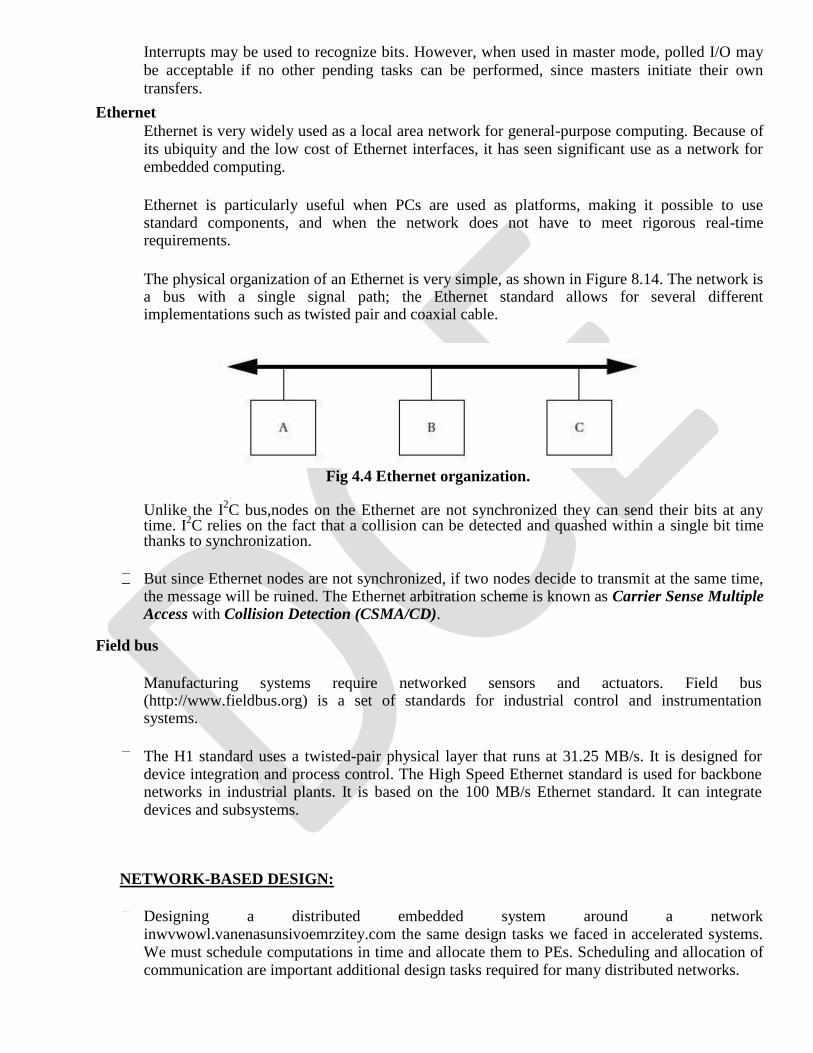
Interrupts may be used to recognize bits. However, when used in master mode, polled I/O may
be acceptable if no other pending tasks can be performed, since masters initiate their own
transfers. Ethernet
Ethernet is very widely used as a local area network for general-purpose computing. Because of its ubiquity and the low cost of Ethernet interfaces, it has seen significant use as a network for embedded computing.
Ethernet is particularly useful when PCs are used as platforms, making it possible to use
standard components, and when the network does not have to meet rigorous real-time requirements.
The physical organization of an Ethernet is very simple, as shown in Figure 8.14. The network is a bus with a single signal path; the Ethernet standard allows for several different implementations such as twisted pair and coaxial cable.
Fig 4.4 Ethernet organization.
Unlike the I2C bus,nodes on the Ethernet are not synchronized they can send their bits at any
time. I2C relies on the fact that a collision can be detected and quashed within a single bit time
thanks to synchronization.
But since Ethernet nodes are not synchronized, if two nodes decide to transmit at the same time, the message will be ruined. The Ethernet arbitration scheme is known as Carrier Sense Multiple Access with Collision Detection (CSMA/CD).
Field bus
Manufacturing systems require networked sensors and actuators. Field bus
(http://www.fieldbus.org) is a set of standards for industrial control and instrumentation systems.
The H1 standard uses a twisted-pair physical layer that runs at 31.25 MB/s. It is designed for device integration and process control. The High Speed Ethernet standard is used for backbone networks in industrial plants. It is based on the 100 MB/s Ethernet standard. It can integrate devices and subsystems.
NETWORK-BASED DESIGN:
Designing a distributed embedded system around a network inwvwowl.vanenasunsivoemrzitey.com the same design tasks we faced in accelerated systems. We must schedule computations in time and allocate them to PEs. Scheduling and allocation of communication are important additional design tasks required for many distributed networks.
Many embedded networks are designed for low cost and therefore do not provide excessively high communication speed. If we are not careful, the network can become the bottleneck in system design. In this section we concentrate on design tasks unique to network-based distributed embedded systems.
We know how to analyze the execution time of programs and systems of processes on single
CPUs, but to analyze the performance of networks we must know how to determine the delay incurred by transmitting messages. Let us assume for the moment that messages are sent reliably we do not have to retransmit a message.
The message delay for a single message with no contention (as would be the case in a point-to-
point connection) can be modeled as
tm = tx + tn + tr (4.1)
where tx is the transmitter-side overhead, tn is the network transmission time, and tr is the receiver-side overhead. In I
2C, tx and tr are negligible relative to tn
If messages can interfere with each other in the network, analyzing communication delay
becomes difficult. In general, because we must wait for the network to become available and then transmit the message, we can write the message delay as
ty = td+ tm (4.2)
where td is the network availability delay incurred waiting for the network to become available.
The main problem, therefore, is calculating td. That value depends on the type of arbitration used in the network.
■ If the network uses fixed-priority arbitration, the network availability delay is unbounded for all but
the highest-priority device. Since the highest-priority device always gets the network first, unless there is an application-specific limit on how long it will transmit before relinquishing the network, it can keep
blocking the other devices indefinitely.
■ If the network uses fair arbitration, the network availability delay is bounded. In the case of round-robin arbitration, if there are N devices, then the worst case network availability delay is N(tx+tarb),where tarb is the delay incurred for arbitration. tarb is usually small compared to transmission time.
Of course,a round-robin arbitrated network puts all communications at the same priority. This does not eliminate the priority inversion problem because processes still have priorities. Thus far we have assumed a single-hop network: A message is received at its intended destination directly from the source,without going through any other network node.
It is possible to build multihop networks in which messages are routed through network nodes www.annauniverzity.com
to get to their destinations. (Using a multistage network does not necessarily mean using a multihop network—the stages in a multistage network are generally much smaller than the network PEs.) Figure 4.5 shows an example of a multihop communication.
The hardware platform has two separate networks ( perhaps so that communications between
subsets of the PEs do not interfere),but there is no direct path from M1 to M5.The message is therefore routed through M3, which reads it from one network and sends it on to the other one.
Analyzing delays through multihop systems is very difficult. For example,the time that the
message is held at M3 depends on both the computational load of M3 and the other messages that it must handle.
If there is more than one network,we must allocate communications to the networks. We may establish multiple networks so that lower-priority communications can be handled separately without interfering with high-priority communications on the primary network.
Scheduling and allocation of computations and communications are clearly interrelated. If we change the allocation of computations, we change not only the scheduling of processes on those PEs but also potentially the schedules of PEs with which they communicate.
For example, if we move a computation to a slower PE, its results will be available later, which
may mean rescheduling both the process that uses the value and the communication that sends the value to its destination.
INTERNET-ENABLED SYSTEMS: Some very different types of distributed embedded system are rapidly emerging the
Internet- enabled embedded system and Internet appliances. The Internet is not well
suited to the real- time tasks that are the bread and butter of embedded computing, but it
does provide a rich environment for non–real-time interaction. In this section we will
discuss the Internet and how it can be used by embedded computing systems.
Internet
The Internet Protocol (IP) [Los97, Sta97A] is the fundamental protocol on the
Internet. It provides connectionless, packet-based communication. Industrial automation has long been a good application area for Internet-based embedded systems.
Information appliances that use the Internet are rapidly becoming another use of IP in embedded computing. Internet protocol is not defined over a particular physical implementation it is an internetworking standard. Internet packets are assumed to be carried by some other network, such as an Ethernet. In general, an Internet packet will travel over several different networks from source to destination.
The IP allows data to flow seamlessly through these networks from one end user to another. The relationship between IP and individual networks is illustrated in Figure 4.6. IP works at the network layer.
When node A wants to send data to node B, the application’s data pass through several layers of
the protocol stack to send to the IP. IP creates packets for routing to the destination, which are
then sent to the data link and physical layers. A node that transmits data among different types
of networks is known as a router.
The router’s functionality must go up to the IP layer, but since it is not running applications, it
does not need to go to higher levels of the OSI model. In general, a packet may go through several routers to get to its destination. At the
destination, the IP layer provides data to the transport layer and ultimately the
receiving application.
As the data pass through several layers of the protocol stack, the IP packet data are
encapsulated in packet formats appropriate to each layer.
The basic format of an IP packet is shown in Figure 4.7. The header and data payload are both of variable length. The maximum total length of the header and data payload is 65,535 bytes.
An Internet address is a number (32 bits in early versions of IP, 128 bits in IPv6). The
IP address is typically written in the form xxx.xx.xx.xx. The names by which users and
applications typically refer to Internet nodes, such as foo.baz.com, are translated into IP
addresses via calls to a Domain Name Server, one of the higher-level services built on
top of IP.
The fact that IP works at the network layer tells us that it does not guarantee that a
packet is delivered to its destination. Furthermore, packets that do arrive may come out of order. This is referred to as best-effort routing.
Since routes for data may change quickly with subsequent along very different paths
with different delays, real-time performance of IP can be hard to predict.
The Transmission Control Protocol (TCP) is one such example. It provides a connection oriented service that ensures that data arrive in the appropriate order, and it uses an acknowledgment protocol to ensure that packets arrive. Because many higher-level services are built on top of TCP, the basic protocol is often referred to as TCP/IP.
Figure 4.8 shows the relationships between IP and higher-level Internet services. Using IP as the foundation, TCP is used to provide File Transport Protocol for batch file transfers, Hypertext Transport Protocol (HTTP) for Worldwide Web service, Simple Mail Transfer Protocol for email, and Telnet for virtual terminals.
A separate transport protocol, User Datagram Protocol, is used as the basis for the network management
provided by the Simple Network Management Protocol

.
Internet Applications
The Internet provides a standard way for an embedded system to act in concert with other
devices and with users, such as:
■ One of the earliest Internet-enabled embedded systems was the laser printer. High-end laser printers often use IP to receive print jobs from host machines.
■ Portable Internet devices can display Web pages, read email, and synchronize calendar information with remote computers.
■ A home control system allows the homeowner to remotely monitor and control home cameras, lights, and so on.
Although there are higher-level services that provide more time-sensitive delivery
mechanisms for the Internet, the basic incarnation of the Internet is not well su
wit
we
wd
.antno
auh
nia
verd
zityr.ce
oa
ml-time operations. However, IP is a very good way to let
the embedded system talk to other systems.
IP provides a way for both special-purpose and standard programs (such as Web
browsers) to talk to the embedded system. This non–real-time interaction can be used to monitor the system, set its configuration, and interact with it.
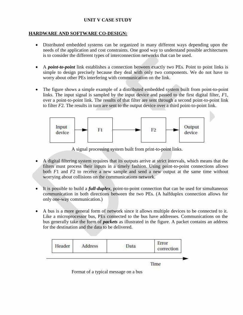
UNIT V CASE STUDY HARDWARE AND SOFTWARE CO-DESIGN:
Distributed embedded systems can be organized in many different ways depending upon the needs of the application and cost constraints. One good way to understand possible architectures is to consider the different types of interconnection networks that can be used.
A point-to-point link establishes a connection between exactly two PEs. Point to point links is simple to design precisely because they deal with only two components. We do not have to worry about other PEs interfering with communication on the link.
The figure shows a simple example of a distributed embedded system built from point-to-point links. The input signal is sampled by the input device and passed to the first digital filter, F1, over a point-to-point link. The results of that filter are sent through a second point-to-point link to filter F2. The results in turn are sent to the output device over a third point-to-point link.
A signal processing system built from print-to-point links.
A digital filtering system requires that its outputs arrive at strict intervals, which means that the filters must process their inputs in a timely fashion. Using point-to-point connections allows both F1 and F2 to receive a new sample and send a new output at the same time without worrying about collisions on the communications network.
It is possible to build a full-duplex, point-to-point connection that can be used for simultaneous communication in both directions between the two PEs. (A halfduplex connection allows for only one-way communication.)
A bus is a more general form of network since it allows multiple devices to be connected to it. Like a microprocessor bus, PEs connected to the bus have addresses. Communications on the bus generally take the form of packets as illustrated in the figure. A packet contains an address for the destination and the data to be delivered.
Format of a typical message on a bus
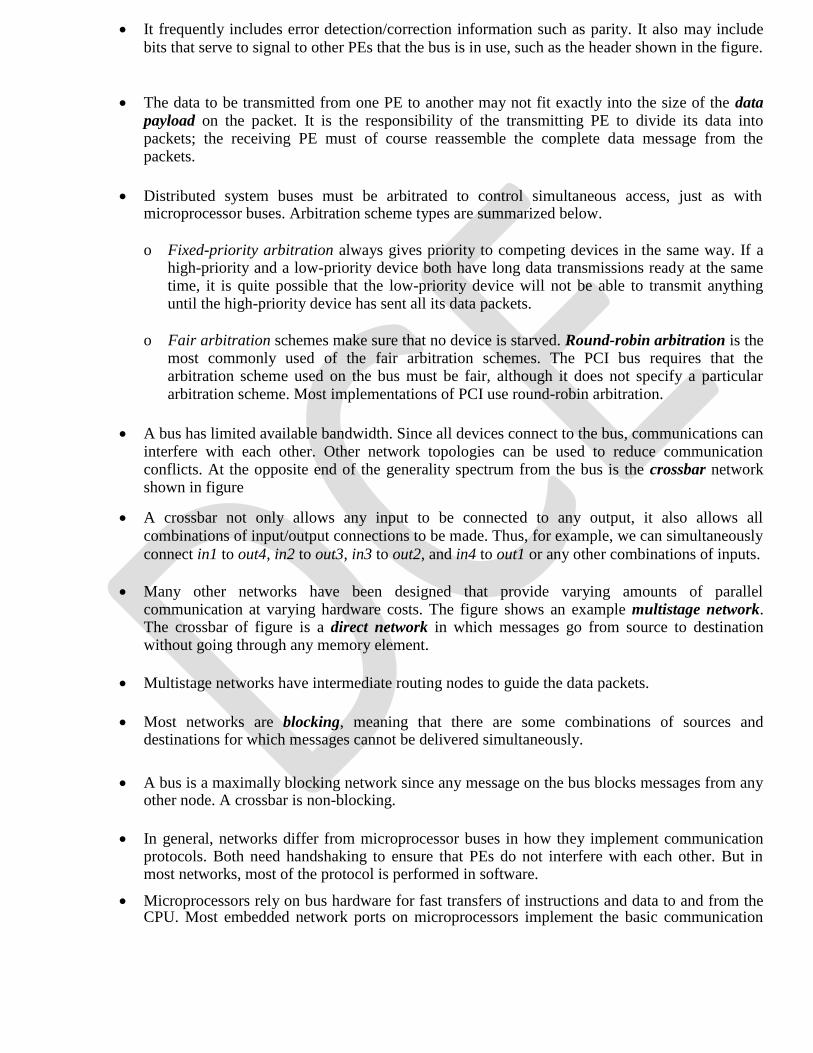
It frequently includes error detection/correction information such as parity. It also may include
bits that serve to signal to other PEs that the bus is in use, such as the header shown in the figure.
The data to be transmitted from one PE to another may not fit exactly into the size of the data payload on the packet. It is the responsibility of the transmitting PE to divide its data into
packets; the receiving PE must of course reassemble the complete data message from the packets.
Distributed system buses must be arbitrated to control simultaneous access, just as with microprocessor buses. Arbitration scheme types are summarized below.
o Fixed-priority arbitration always gives priority to competing devices in the same way. If a
high-priority and a low-priority device both have long data transmissions ready at the same time, it is quite possible that the low-priority device will not be able to transmit anything until the high-priority device has sent all its data packets.
o Fair arbitration schemes make sure that no device is starved. Round-robin arbitration is the
most commonly used of the fair arbitration schemes. The PCI bus requires that the arbitration scheme used on the bus must be fair, although it does not specify a particular arbitration scheme. Most implementations of PCI use round-robin arbitration.
A bus has limited available bandwidth. Since all devices connect to the bus, communications can interfere with each other. Other network topologies can be used to reduce communication conflicts. At the opposite end of the generality spectrum from the bus is the crossbar network shown in figure
A crossbar not only allows any input to be connected to any output, it also allows all
combinations of input/output connections to be made. Thus, for example, we can simultaneously
connect in1 to out4, in2 to out3, in3 to out2, and in4 to out1 or any other combinations of inputs.
Many other networks have been designed that provide varying amounts of parallel communication at varying hardware costs. The figure shows an example multistage network. The crossbar of figure is a direct network in which messages go from source to destination without going through any memory element.
Multistage networks have intermediate routing nodes to guide the data packets.
Most networks are blocking, meaning that there are some combinations of sources and destinations for which messages cannot be delivered simultaneously.
A bus is a maximally blocking network since any message on the bus blocks messages from any other node. A crossbar is non-blocking.
In general, networks differ from microprocessor buses in how they implement communication protocols. Both need handshaking to ensure that PEs do not interfere with each other. But in most networks, most of the protocol is performed in software.
Microprocessors rely on bus hardware for fast transfers of instructions and data to and from the
CPU. Most embedded network ports on microprocessors implement the basic communication
functions (such as driving the communications medium) in hardware and implement many other operations in software.
An alternative to a non-bus network is to use multiple networks. As with PEs, it may be cheaper to use two slow, inexpensive networks than a single high performance, expensive network.
If we can segregate critical and noncritical communications onto separate networks, it may be possible to use simpler topologies such as buses. Many systems use serial links for low-speed communication and CPU buses for higher speed and volume data transfers.
DATA COMPRESSOR:
Requirements and Algorithm
We use the Huffman coding technique; we require some understanding of how our compression code fits into a larger system. The figure shows a collaboration diagram for the data compression process.
The data compressor takes in a sequence of input symbols and then produces a stream of output symbols. Assume for simplicity that the input symbols are one byte in length. The output symbols are variable length, so we have to choose a format in which to deliver the output data.
Delivering each coded symbol separately is tedious, since we would have to supply the length of
each symbol and use external code to pack them into words.
On the other hand, bit-by-bit delivery is almost certainly too slow. Therefore, we will rely on the data compressor to pack the coded symbols into an array. There is not a one-to-one relationship between the input and output symbols, and we may have to wait for several input symbols before a packed output word comes out.
The data compressor as discussed above is not a complete system, but we can create at least a partial requirements list for the module as seen below. We used the abbreviation N/A for not applicable to describe some items that do not make sense for a code module.
Specification
Let’s refine the description of Figure 3.20 to come up with a more complete specification for our
data compression module. That collaboration diagram concentrates on the steady-state behavior
of the system.
For a fully functional system, we have to provide the following additional behavior.
o We have to be able to provide the compressor with a new symbol table.
o We should be able to flush the symbol buffer to cause the system to release all pending
symbols that have been partially packed. We may want to do this when we change the symbol table or in the middle of an encoding session to keep a transmitter busy.
A class description for this refined understanding of the requirements on the module is shown in the figure. The class’s buffer and current-bit behaviors keep track of the state of the encoding, and the table attribute provides the current symbol table.
The class has three methods as follows:
o Encode performs the basic encoding function. It takes in a 1-byte input symbol and
returns two values: a boolean showing whether it is returning a full buffer and, if the
Boolean is true, the full buffer itself.
o New-symbol-table installs a new symbol table into the object and throws away
the current contents of the internal buffer.
o Flush returns the current state of the buffer, including the number of valid bits in the buffer.
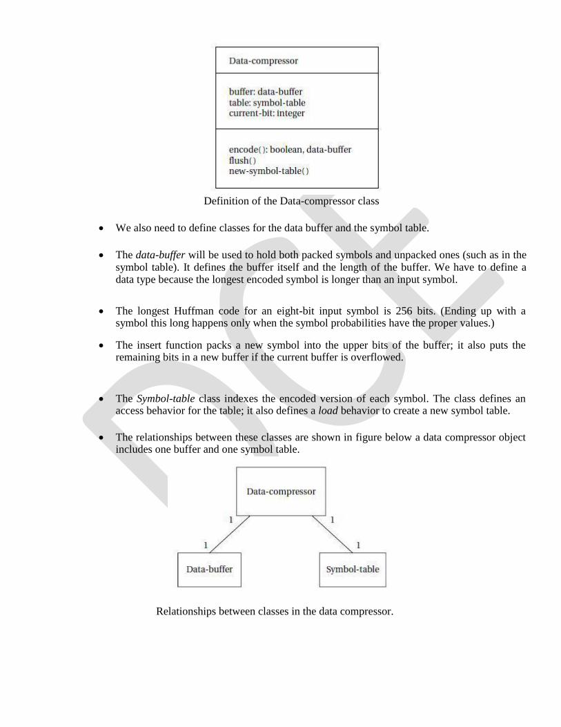
Definition of the Data-compressor class
We also need to define classes for the data buffer and the symbol table.
The data-buffer will be used to hold both packed symbols and unpacked ones (such as in the symbol table). It defines the buffer itself and the length of the buffer. We have to define a data type because the longest encoded symbol is longer than an input symbol.
The longest Huffman code for an eight-bit input symbol is 256 bits. (Ending up with a symbol this long happens only when the symbol probabilities have the proper values.)
The insert function packs a new symbol into the upper bits of the buffer; it also puts the
remaining bits in a new buffer if the current buffer is overflowed.
The Symbol-table class indexes the encoded version of each symbol. The class defines an access behavior for the table; it also defines a load behavior to create a new symbol table.
The relationships between these classes are shown in figure below a data compressor object includes one buffer and one symbol table.
Relationships between classes in the data compressor.
Software Modem:
Low-cost modems generally use specialized chips, but some PCs implement the modem functions in software. Before jumping into the modem design itself, we discuss principles of how to transmit digital data over a telephone line. We will then go through a specification and discuss architecture, module design, and testing.
Theory of Operation and Requirements
The modem will use frequency-shift keying (FSK), a technique used in 1200-baud modems. Keying alludes to Morse code—style keying. The FSK scheme transmits sinusoidal tones, with 0 and 1 assigned to different frequencies.
Sinusoidal tones are much better suited to transmission over analog phone lines than are the traditional high and low voltages of digital circuits. The 01 bit patterns create the chirping sound characteristic of modems. (Higher-speed modems are backward compatible with the 1200-baud FSK scheme and begin a transmission with a protocol to determine which speed and protocol should be used.)
One filter passes frequencies in the range that represents a 0 and rejects the 1-band frequencies,
and the other filter does the converse.
o The outputs of the filters are sent to detectors, which compute the average value of the
signal over the past n samples. When the energy goes above a threshold value, the appropriate bit is detected.
We will send data in units of 8-bit bytes. The transmitting and receiving modems agree in advance on the length of time during which a bit will be transmitted (otherwise known as the baud rate). But the transmitter and receiver are physically separated and therefore are not synchronized in any way.
The receiving modem does not know when the transmitter has started to send a byte. Furthermore, even when the receiver does detect a transmission, the clock rates of the transmitter and receiver may vary somewhat, causing them to fall out of sync. In both cases, we can reduce the chances for error by sending the waveforms for a longer time.
The receiver will detect the start of a byte by looking for a start bit, which is always 0.
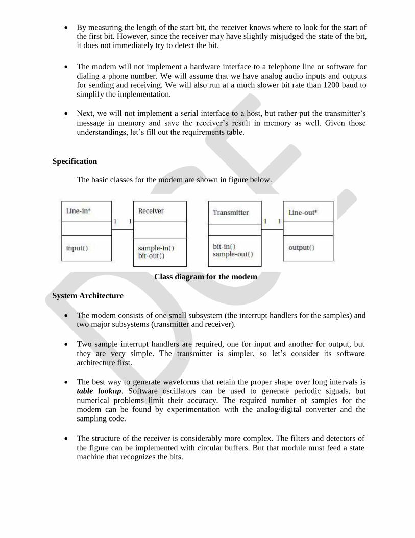
By measuring the length of the start bit, the receiver knows where to look for the start of the first bit. However, since the receiver may have slightly misjudged the state of the bit, it does not immediately try to detect the bit.
The modem will not implement a hardware interface to a telephone line or software for dialing a phone number. We will assume that we have analog audio inputs and outputs for sending and receiving. We will also run at a much slower bit rate than 1200 baud to simplify the implementation.
Next, we will not implement a serial interface to a host, but rather put the transmitter’s
message in memory and save the receiver’s result in memory as well. Given those
understandings, let’s fill out the requirements table.
Specification
The basic classes for the modem are shown in figure below.
Class diagram for the modem
System Architecture
The modem consists of one small subsystem (the interrupt handlers for the samples) and two major subsystems (transmitter and receiver).
Two sample interrupt handlers are required, one for input and another for output, but they are very simple. The transmitter is simpler, so let’s consider its software
architecture first.
The best way to generate waveforms that retain the proper shape over long intervals is table lookup. Software oscillators can be used to generate periodic signals, but numerical problems limit their accuracy. The required number of samples for the modem can be found by experimentation with the analog/digital converter and the sampling code.
The structure of the receiver is considerably more complex. The filters and detectors of the figure can be implemented with circular buffers. But that module must feed a state machine that recognizes the bits.
The recognizer state machine must use a timer to determine when to start and stop computing the filter output average based on the starting point of the bit. It must then determine the nature of the bit at the proper interval. It must also detect the start bit and measure it using the counter.
The receiver sample interrupt handler is a natural candidate to double as the receiver
timer since the receiver’s time points are relative to samples.
The hardware architecture is relatively simple. In addition to the analog/digital and digital/analog converters, a timer is required. The amount of memory required to implement the algorithms is relatively small.
PERSONAL DIGITAL ASSISTANTS
A personal digital assistant (PDA), or handheld computer, is a small, mobile, handheld device that provides computing and information storage/retrieval capabilities.
The vast majority of PDAs have five basic functions: o Contact management (names and addresses) o Scheduling (calendar) o Mobile phone functionality o To do list o Note-taking
Many PDA manufacturers now include additional functionality in their products, such as:
Access to the Internet The ability to play MP3 files The ability to read electronic books The ability to play games Bluetooth connectivity
Size and Weight
The size and weight of PDAs can vary enormously – some are the size of a credit card,
some fit in the palm of the hand and some are like UMPCs. Basic PDAs are confined to
basic information organization, while the latest PDAs have many additional functions
and capabilities such as Bluetooth, Wi-Fi, GPS and extra memory storage options.
Additional options one should consider purchasing include an external Bluetooth keyboard, an extra battery, docking cradle, travel synchronization cable, extra stylus, case, USB/VGA cable for use with a data projector.
Broadly speaking, there are two types of PDA:
• Clamshell PDAs have a small keyboard and they open out rather like a miniature laptop.
They may also feature touch-sensitive screens and a stylus.
• Tablet-type PDAs do not have an integrated keyboard. Input occurs using a stylus or fold-
away/portable keyboard and they tend to be palm-sized.
SET–TOP–BOX:
The continuing trend is to link broadband signal delivery to the home entertainment display, and other devices via set top boxes. Set top boxes used to be just an analog cable tuner/decoder but now it includes the likes of digital cable, satellite controller, internet service controllers, digital video recording systems and home networking.
These devices allow the various cable and satellite signal operators to deliver a wide variety of services from television to internet and the hardware manufacturers can provide many features and benefits including home networking capabilities.
There is digital video recording onto hard disk drives, replacing the cassette format, allowing pause and replay of and live television, or interactive TV. There are new standards being created to facilitate the design of the boxes such as a recent reference blueprint development by communications chipmaker Broadcom using the Microsoft interactive TV software system.
The set top box is going to be a high volume commodity with many forms and
functions. SYSTEM-ON-SILICON:
A system on a chip or system on chip (SoC or SOC) is an integrated circuit (IC) that
integrates all components of a computer or other electronic system into a single chip. It may
contain digital, analog, mixed-signal, and often radio-frequency functions—all on a single chip
substrate. SoCs are very common in the mobile electronics market because of their low power
consumption. A typical application is in the area of embedded systems.
The contrast with a microcontroller is one of degree. Microcontrollers typically have under
100 kB of RAM (often just a few kilobytes) and often really are single-chip-systems, whereas the term SoC is typically used for more powerful processors, capable of running software such as the desktop versions of Windows and Linux, which need external memory chips (flash, RAM) to be useful, and which are used with various external peripherals.
For larger systems, the term system on a chip is hyperbole, indicating technical direction
more than reality: a high degree of chip integration, leading toward reduced manufacturing costs, and the production of smaller systems. Many interesting systems are too complex to fit on
just one chip built with a process optimized for just one of the system's tasks.
When it is not feasible to construct a SoC for a particular application, an alternative is a
system in package (SiP) comprising a number of chips in a single package. In large volumes, SoC is believed to be more cost-effective than SiP since it increases the yield of the fabrication
and because its packaging is simpler.

Another option, as seen for example in higher end cell phones and on the BeagleBoard, is package on package stacking during board assembly. The SoC chip includes processors and numerous digital peripherals, and comes in a ball grid package with lower and upper connections.
The lower balls connect to the board and various peripherals, with the upper balls in a ring holding the memory buses used to access NAND flash and DDR2 RAM. Memory
packages could come from multiple vendors.
FOSS TOOLS FOR EMBEDDED SYSTEM DEVELOPMENT:
Free and open-source software (FOSS) is computer software that can be classified as
both free software and open source software. That is, anyone is freely licensed to use, copy,
study, and change the software in any way, and the source code is openly shared so that people
are encouraged to voluntarily improve the design of the software. This is in contrast to
proprietary software, where the software is under restrictive copyright and the source code is
usually hidden from the users.
The benefits of using FOSS can include decreasing software costs, increasing security and stability (especially in regard to malware), protecting privacy, and giving users more
control over their own hardware.
Free, open-source operating systems such as Linux and descendants of BSD are widely
utilized today, powering millions of servers, desktops, smart phones (e.g. Android), and other
devices. Free software licenses and open-source licenses are used by many software packages.