Embed Size (px)
Citation preview


Corporate Office: 44-A/1, Kalu Sarai, New Delhi-16 | Email : [email protected] | Visit: www.madeeasy.in
GATE-2015 | Electronics Engg.31st January 2015 • Afternoon Session
1234567890123456789012345678901234567890123456789012345678901234567890123456789012345678901234567890123456789012345678901234567890
Page1
Section - I (General Aptitude)
Q.1 Choose the word most similar in meaning to the given word:Awkward(a) Inept (b) Graceful(c) Suitable (d) Dreadful
Ans. (a)
Q.2 Choose the appropriate word/phase, out of the four options given below, to completethe following sentence:Dhoni, as well as the other team members of the Indian team_____present onthe occasion.(a) were (b) was(c) has (d) have
Ans. (b)
Q.3 An electric bus has onboard instruments that report the total electricity consumedsince the start of the trip as well as the total distance covered. During a singleday of operation, the bus travels on stretches M, N, O and P, in that order. Thecumulative distance travelled and the corresponding electricity consumption areshown in the Table below:
Stretch Cumulative distance(km)
Electricity used(kWh)
M
N
O
P
2045
75100
1225
4557
The stretch where the electricity consumption per km is minimum is(a) M (b) N(c) O (d) P
Ans. (d)
Q.4 What is the adverb for the given word below?Misogynous(a) Misogynousness (b) Misogynity(c) Misogynously (d) Misogynous
Ans. (*)

Corporate Office: 44-A/1, Kalu Sarai, New Delhi-16 | Email : [email protected] | Visit: www.madeeasy.in
GATE-2015 | Electronics Engg.1st February 2015 • Afternoon Session
1234567890123456789012345678901234567890123456789012345678901234567890123456789012345678901234567890123456789012345678901234567890
Page2
Q.5 Ram and Ramesh appeared in an interview for two vacancies in the samedepartment. The probability of Ram’s selection is 1/6 and that of Ramesh is 1/8. What is the probability that only one of them will be selected?(a) 47/48 (b) 1/4(c) 13/48 (d) 35/48
Ans. (b)
Q.6 Given below are two statements followed by two conclusions. Assuming thesestatements to be true, decide which one logically follows.Statements:I. All film star are playback singers.II. All film directors are film stars.Conclusions:I. All film directors are playback singers.II. Some film stars are film directors.(a) Only conclusion I follows. (b) Only conclusion I nor II follows.(c) Neither conclusion I nor II follows. (d) Both conclusions I and II follow.
Ans. (d)
Q.7 In the following sentence certain parts are underlined and marked P, Q and R.One of the parts may contain certain error or may not be acceptable in standardwritten communication. Select the part containing an error. Choose D as youranswer if there is no error.
The student concreted all the errors that the instructor marked on the answerbook.(a) P (b) Q(c) R (d) No Error
Ans. (b)
Q.8 If a2 + b2 + c = 1, then ab + bc + ac lies in the interval(a) [1, 2/3] (b) [–1/2, 1](c) [–1, 1/2] (d) [2, –4]
Ans. (b)

Corporate Office: 44-A/1, Kalu Sarai, New Delhi-16 | Email : [email protected] | Visit: www.madeeasy.in
GATE-2015 | Electronics Engg.31st January 2015 • Afternoon Session
1234567890123456789012345678901234567890123456789012345678901234567890123456789012345678901234567890123456789012345678901234567890
Page3
Q.9 Lamenting the gradual sidelining of the arts in school curricula, a group ofprominent artists wrote to the Chief Minister last year, asking him to allocatemore funds to support arts education in schools. However, no such increase hasbeen announced in this year’s Budget. The artists expressed their deep anguishat their request not being approved, but many of them remain optimistic aboutfinding in the future.Which of the statement(s) below is/are logically valid and can be inferred fromthe above statements?(i) The artists expected funding for the arts to increase this year.(ii) The Chief Minister was receptive to the idea of increasing funding for the
arts.(iii) The Chief Minister is a prominent artists.(iv) Schools are giving less importance to arts education nowadays.(a) (iii) and (iv) (b) (i) and (iv)(c) (i), (ii) and (iv) (d) (i) and (iii)
Ans. (b)
Q.10 A tiger is 50 leaps of its own behind a deer. The tiger takes 5 leaps per minuteto the deer’s 4. If the tiger and the deer cover 8 metre and 5 metre per leaprespectively, what distance in metres will the tiger have to run before it catchesthe deer?
Ans. (800)
Section - II (Electronics Engineering)
Q.1 The general solution of the differential equation dy 1+ cos y=dx 1 - cos x
22
is
(a) tan y – cot x = c (c is a constant) (b) tan x – cot y = c (c is a constant)(c) tan y + cot x = c (c is a constant) (d) tan x + cot y = c (c is a constant)
Ans. (c)
Q.2 Two causal discrete-time signals x[n] and y[n] are related as y[n] = [∑n
m=x m
0] . If
the z-transform of y[n] is 22
z(z -1), the value of x[2] is _____.
Ans. (0)

Corporate Office: 44-A/1, Kalu Sarai, New Delhi-16 | Email : [email protected] | Visit: www.madeeasy.in
GATE-2015 | Electronics Engg.1st February 2015 • Afternoon Session
1234567890123456789012345678901234567890123456789012345678901234567890123456789012345678901234567890123456789012345678901234567890
Page4
Q.3 A unity negative feedback system has an open-loop transfer function G(s) = K
s(s + )10 .the gain K for the system to have a damping ratio of 0.25 is _____.
Ans. (400)
Q.4 For the signal flow graph shown in the figure, the value of ( )( )
C sR s is
R s( ) C s( )X11
G1 G2X2
X3 1 X4
X5 G4G3
–H2–H1
–H3
(a) +G G G G
G G H G G H G G H G G G G H H1 2 3 4
1 2 1 3 4 2 2 3 3 1 2 3 4 1 21 – – –
(b) +G G G G
G G H G G H G G H G G G G H H1 2 3 4
1 2 1 3 4 2 2 3 3 1 2 3 4 1 21 + + +
(c) +G G H G G H G G H G G G G H H1 2 1 3 4 2 2 3 3 1 2 3 4 1 2
11 + + +
(d)1
+G G H G G H G G H G G G G H H1 2 1 3 4 2 2 3 3 1 2 3 4 1 21 – – –
Ans. (b)
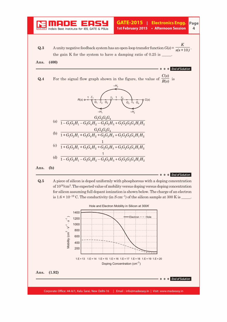
Q.5 A piece of silicon is doped uniformly with phosphorous with a doping concentrationof 1016/cm3. The expected value of mobility versus doping versus doping concentrationfor silicon assuming full dopant ionization is shown below. The charge of an electronis 1.6 × 10⁻¹⁹ C. The conductivity (in S cm–1) of the silicon sample at 300 K is _____.
1.E + 13 1.E + 14 1.E + 15 1.E + 16 1.E + 17 1.E + 18 1.E + 19 1.E + 20
1400
1200
1000
800
600
400
200
Electron Hole
Hole and Electron Mobility in Silicon at 300K
Doping Concentration (cm )–3
Mob
ility
(cm
)
21
1⋅ V
s ⋅
––
Ans. (1.92)
Corporate Office: 44-A/1, Kalu Sarai, New Delhi-16 | Email : [email protected] | Visit: www.madeeasy.in
GATE-2015 | Electronics Engg.31st January 2015 • Afternoon Session
1234567890123456789012345678901234567890123456789012345678901234567890123456789012345678901234567890123456789012345678901234567890
Page5
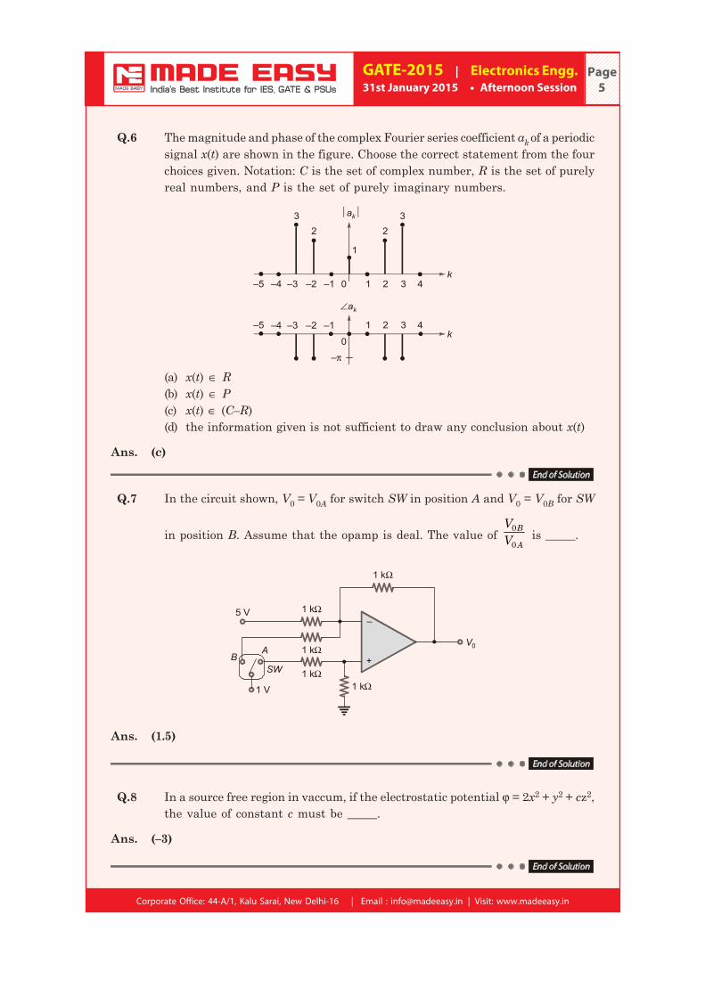
Q.6 The magnitude and phase of the complex Fourier series coefficient ak of a periodicsignal x(t) are shown in the figure. Choose the correct statement from the fourchoices given. Notation: C is the set of complex number, R is the set of purelyreal numbers, and P is the set of purely imaginary numbers.
k–5 –4 –3 –2 –1 0 1 2 3 4
23 3
2
1
⏐ak⏐
k–5 –4 –3 –2 –1
0
1 2 3 4
∠ak
–π
(a) x(t) ∈ R(b) x(t) ∈ P(c) x(t) ∈ (C–R)(d) the information given is not sufficient to draw any conclusion about x(t)
Ans. (c)
Q.7 In the circuit shown, V0 = V0A for switch SW in position A and V0 = V0B for SW
in position B. Assume that the opamp is deal. The value of B
A
VV
0
0 is _____.
–
+1 kΩ
1 kΩ
1 kΩ
1 kΩ
V0
BA
1 V
5 V
1 kΩ
SW
Ans. (1.5)
Q.8 In a source free region in vaccum, if the electrostatic potential ϕ = 2x2 + y2 + cz2,the value of constant c must be _____.
Ans. (–3)

Corporate Office: 44-A/1, Kalu Sarai, New Delhi-16 | Email : [email protected] | Visit: www.madeeasy.in
GATE-2015 | Electronics Engg.1st February 2015 • Afternoon Session
1234567890123456789012345678901234567890123456789012345678901234567890123456789012345678901234567890123456789012345678901234567890
Page6
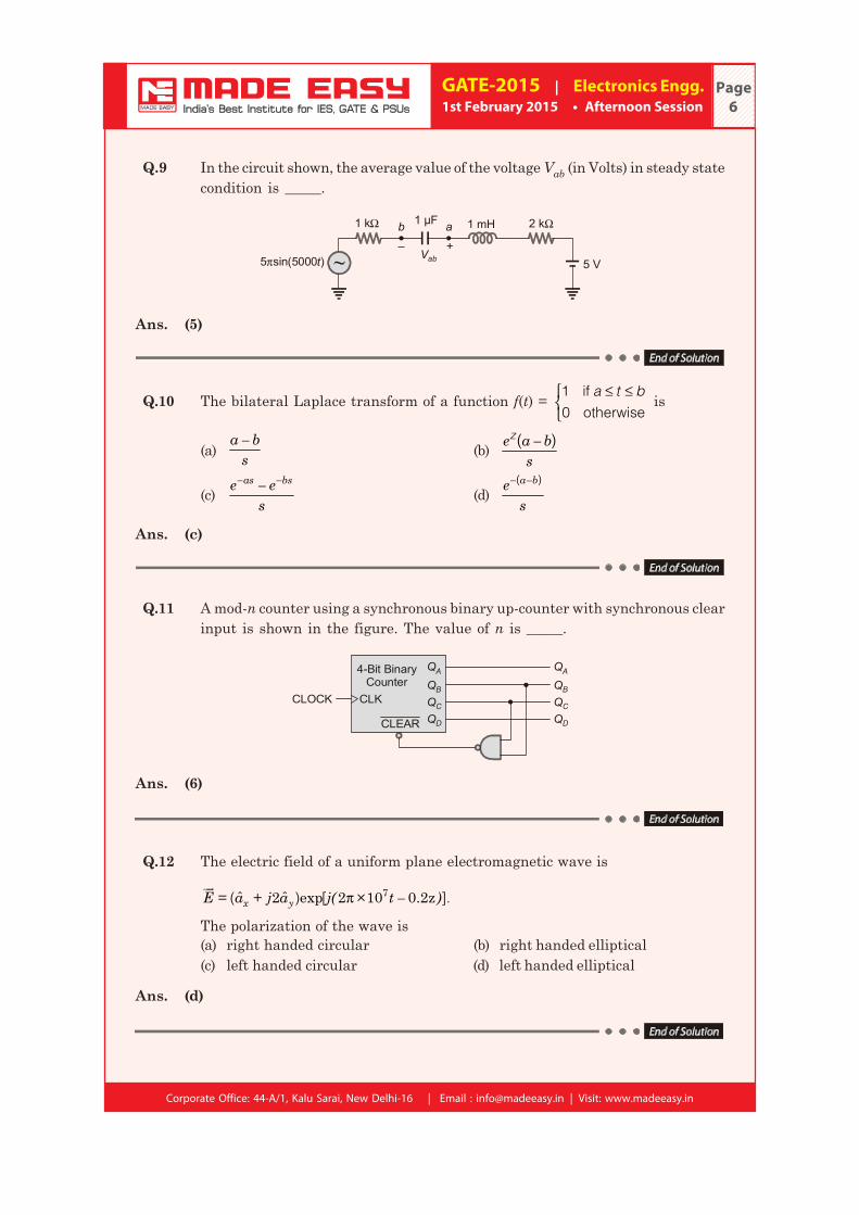
Q.9 In the circuit shown, the average value of the voltage Vab (in Volts) in steady statecondition is _____.
1 kΩ b a1 µF 1 mH 2 kΩ
5 sin(5000 )π t 5 V– +
Vab
Ans. (5)
Q.10 The bilateral Laplace transform of a function f(t) = 1 if
0 otherwise
a t b≤ ≤⎧⎨⎩
is
(a) a – bs (b) ( )ze a – b
s
(c)− −as bse – e
s(d)
( )− a–bes
Ans. (c)
Q.11 A mod-n counter using a synchronous binary up-counter with synchronous clearinput is shown in the figure. The value of n is _____.
QD
QC
QB
QA
QD
QC
QB
QA4-Bit BinaryCounter
CLKCLOCK
CLEAR
Ans. (6)
Q.12 The electric field of a uniform plane electromagnetic wave is
ˆ ˆ( ) [ ].π���
x yE = a + j a j( × t – )72 exp 2 10 0.2z
The polarization of the wave is(a) right handed circular (b) right handed elliptical(c) left handed circular (d) left handed elliptical
Ans. (d)
Corporate Office: 44-A/1, Kalu Sarai, New Delhi-16 | Email : [email protected] | Visit: www.madeeasy.in
GATE-2015 | Electronics Engg.31st January 2015 • Afternoon Session
1234567890123456789012345678901234567890123456789012345678901234567890123456789012345678901234567890123456789012345678901234567890
Page7
Q.13 The signal π⎛ ⎞π⎜ ⎟⎝ ⎠t +cos 10
4 is ideally sampled at a sampling frequency of 15 Hz.
The sampled signal is passed through a filter with impulse responseπ π⎛ ⎞ ⎛ ⎞π⎜ ⎟ ⎜ ⎟⎝ ⎠ ⎝ ⎠πt t –
tsin( ) cos 40
2. The filter output is
(a)π⎛ ⎞π⎜ ⎟⎝ ⎠
t –15 cos 402 4 (b) π π⎛ ⎞ ⎛ ⎞π⎜ ⎟ ⎜ ⎟⎝ ⎠ ⎝ ⎠π
15 sin( ) cos 102 4
t t +t
(c) π⎛ ⎞π⎜ ⎟⎝ ⎠t –15 cos 10
2 4(d) π π⎛ ⎞ ⎛ ⎞π⎜ ⎟ ⎜ ⎟⎝ ⎠ ⎝ ⎠π
15 sin( ) cos 102 2
t t –t
Ans. (a)
Q.14 A sinusoidal signal of amplitude A is quantized by a uniform quantizer. Assumethat the signal utilizes all the representation levels of the quantizer. If the signalto quantization noise ratio is 31.8 dB, the number of levels in the quantizer is____.
Ans. (32)
Q.15 Let the signal f(t) = 0 outside the interval [T1, T2], where T1 and T2 are finite.Furthermore, ⎪f(t)⎪ < ∞. The region of convergence (RoC) of the signal’s bilateralLaplace transform F(s) is(a) a parallel strip containing the jΩ axis(b) a parallel strip not containing the jΩ axis(c) the entire s-plane(d) a half plane containing the jΩ axis
Ans. (c)
Q.16 The 2-port admittance matrix of the circuit shown is given by5 Ω
10 Ω 10 Ω
(a) ⎡ ⎤⎢ ⎥⎣ ⎦
0.3 0.20.2 0.3
(b)⎡ ⎤⎢ ⎥⎣ ⎦
15 55 15
(c) ⎡ ⎤⎢ ⎥⎣ ⎦
3.33 55 3.33 (d)
⎡ ⎤⎢ ⎥⎣ ⎦
0.3 0.40.4 0.3
Ans. (a)

Corporate Office: 44-A/1, Kalu Sarai, New Delhi-16 | Email : [email protected] | Visit: www.madeeasy.in
GATE-2015 | Electronics Engg.1st February 2015 • Afternoon Session
1234567890123456789012345678901234567890123456789012345678901234567890123456789012345678901234567890123456789012345678901234567890
Page8
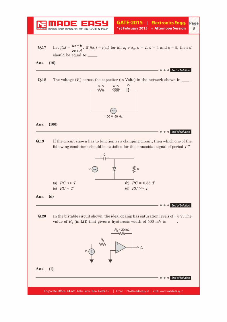
Q.17 Let f(z) = a + bc + d
zz
. If f(z1) = f(z2) for all z1 ≠ z2, a = 2, b = 4 and c = 5, then d
should be equal to _____.
Ans. (10)
Q.18 The voltage (Vc) across the capacitor (in Volts) in the network shown in ____ .80 V 40 V VC
100 V, 50 Hz
Ans. (100)
Q.19 If the circuit shown has to function as a clamping circuit, then which one of thefollowing conditions should be satisfied for the sinusoidal signal of period T ?
C+ –
V R
(a) RC << T (b) RC = 0.35 T(c) RC ≈ T (d) RC >> T
Ans. (d)
Q.20 In the bistable circuit shown, the ideal opamp has saturation levels of ± 5 V. Thevalue of R1 (in kΩ) that gives a hysteresis width of 500 mV is _____.
+
–
R2 = 20 kΩ
R1
+–ViVo
Ans. (1)

Corporate Office: 44-A/1, Kalu Sarai, New Delhi-16 | Email : [email protected] | Visit: www.madeeasy.in
GATE-2015 | Electronics Engg.31st January 2015 • Afternoon Session
1234567890123456789012345678901234567890123456789012345678901234567890123456789012345678901234567890123456789012345678901234567890
Page9
Q.21 In the figure shown, the output Y is required to be Y = A B + CD . The gatesG1 and G2 must be,
CD
G2
G1A
BY
(a) NOR, OR (b) OR, NAND(c) NAND, OR (d) AND, NAND
Ans. (a)
Q.22 An n-type silicon sample is uniformly illuminated with light which generates 1020
electron-hole pairs per cm3 per second. The minority carrier lifetime in the sampleis 1 μs. In the steady state, the hole concentration in the sample is approximately10x, where x is an integer. The value of x is _____.
Ans. (14)
Q.23 The value of x for which all the eigen-values of the matrix given below are real is⎡ ⎤⎢ ⎥⎢ ⎥⎢ ⎥⎣ ⎦
jx
10 5 + 420 2
4 2 –10(a) 5 + j (b) 5 – j(c) 1 – 5j (d) 1 + 5j
Ans. (a)
Q.24 In an 8085 microprocessor, which one of the following instructions changes thecontent of the accumulator?(a) MOV B, M (b) PCHL(c) RNZ (d) SBI BEH
Ans. (d)

Corporate Office: 44-A/1, Kalu Sarai, New Delhi-16 | Email : [email protected] | Visit: www.madeeasy.in
GATE-2015 | Electronics Engg.1st February 2015 • Afternoon Session
1234567890123456789012345678901234567890123456789012345678901234567890123456789012345678901234567890123456789012345678901234567890
Page10
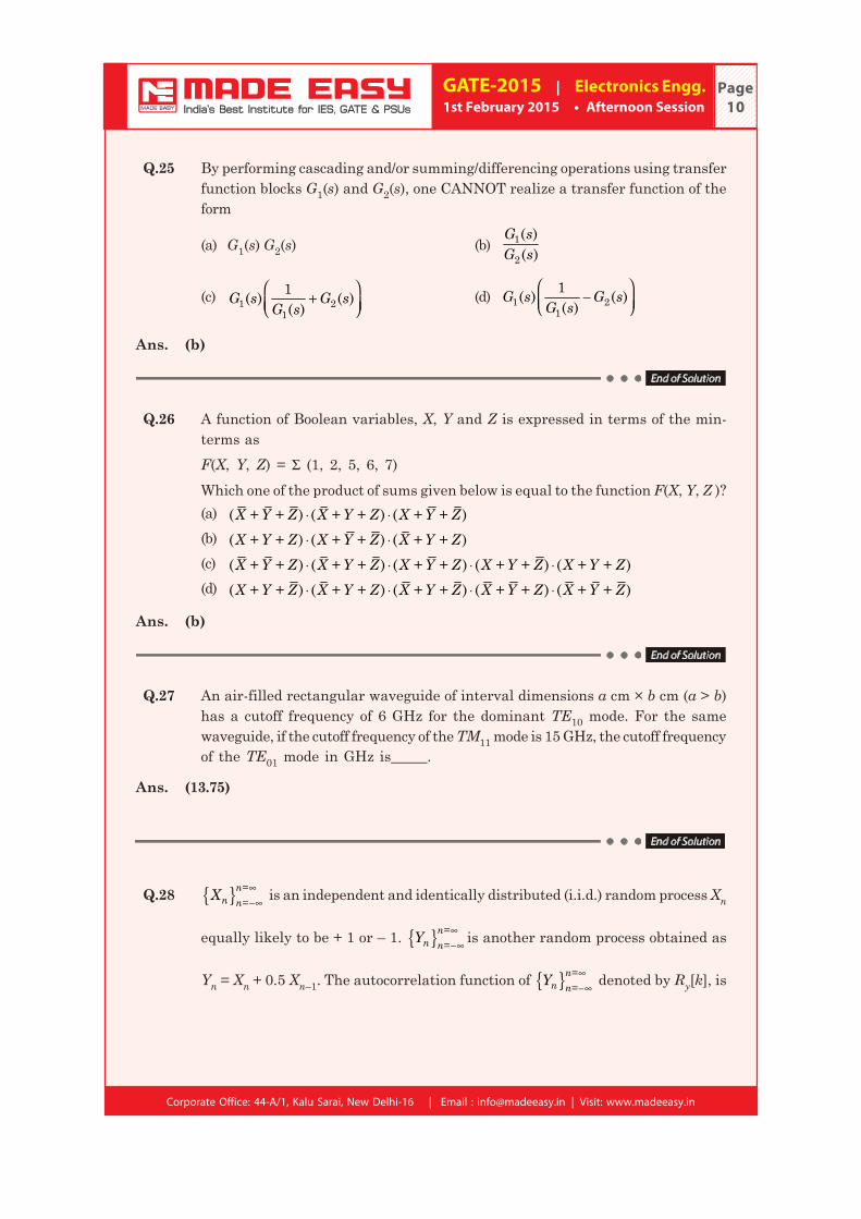
Q.25 By performing cascading and/or summing/differencing operations using transferfunction blocks G1(s) and G2(s), one CANNOT realize a transfer function of theform
(a) G1(s) G2(s) (b)G sG s
1
2
( )( )
(c) ⎛ ⎞+⎜ ⎟⎝ ⎠
G s G sG s1 2
1
1( ) ( )( )
(d) ⎛ ⎞−⎜ ⎟⎝ ⎠
G s G sG s1 2
1
1( ) ( )( )
Ans. (b)
Q.26 A function of Boolean variables, X, Y and Z is expressed in terms of the min-terms asF(X, Y, Z) = Σ (1, 2, 5, 6, 7)Which one of the product of sums given below is equal to the function F(X, Y, Z )?(a) ⋅ ⋅X + Y + Z X + Y + Z X + Y + Z( ) ( ) ( )(b) ⋅ ⋅X + Y + Z X + Y + Z X + Y + Z( ) ( ) ( )(c) ⋅ ⋅ ⋅ ⋅X + Y + Z X + Y + Z X + Y + Z X + Y + Z X + Y + Z( ) ( ) ( ) ( ) ( )(d) ⋅ ⋅ ⋅ ⋅X + Y + Z X + Y + Z X + Y + Z X + Y + Z X + Y + Z( ) ( ) ( ) ( ) ( )
Ans. (b)
Q.27 An air-filled rectangular waveguide of interval dimensions a cm × b cm (a > b)has a cutoff frequency of 6 GHz for the dominant TE10 mode. For the samewaveguide, if the cutoff frequency of the TM11 mode is 15 GHz, the cutoff frequencyof the TE01 mode in GHz is_____.
Ans. (13.75)
Q.28 { } ∞∞
n=n n=–X is an independent and identically distributed (i.i.d.) random process Xn
equally likely to be + 1 or – 1. { } ∞∞
n=n n=–Y is another random process obtained as
Yn = Xn + 0.5 Xn–1. The autocorrelation function of { } ∞∞
n=n n=–Y denoted by Ry[k], is

Corporate Office: 44-A/1, Kalu Sarai, New Delhi-16 | Email : [email protected] | Visit: www.madeeasy.in
GATE-2015 | Electronics Engg.31st January 2015 • Afternoon Session
1234567890123456789012345678901234567890123456789012345678901234567890123456789012345678901234567890123456789012345678901234567890
Page11
(a)
1
–3 –2 –1 0 1 2 3 k
R kY [ ]
⋅⋅⋅ (b)
1.25
–3 –2 –1 0 1 2 3 k
R kY [ ]0.5 0.5
⋅⋅⋅
(c)
1.25
–3 –2 –1 0 1 2 3 k
R kY [ ]0.5 0.5
⋅⋅⋅ 0.25 0.25(d)
1.25
–3 –2 –1 0 1 2 3 k
R kY [ ]
⋅⋅⋅ 0.25 0.25
Ans. (c)
Q.29 In MOS capacitor with an oxide layer thickness of 10 mm. The maximumdepletion layer thickness is 100 mm. The permittivities of the semiconductor andthe oxide layer are εs and εox respectively. Assuming εs/εox = 3 the ratio of themaximum capacitance to the minimum capacitance of this MOS capacitor is______.
Ans. (4.33)
Q.30 An LC tank circuit consists of an ideal capacitor C connected in parallel witha coil of inductance L having an internal resistance R. The resonant frequencyof the tank circuit is
(a) π LC1
2 (b)π
CRLLC
21 1 –2
(c) 2CπL
RLC1 1 –
2 (d) 2
πCRLLC
1 1 –2
Ans. (b)
Q.31 Let the random variable X represent the number of times a fair coin needs to be tossedtill two consecutive heads appear for the first time. The expectation of X is_____.
Ans. (1.5)

Corporate Office: 44-A/1, Kalu Sarai, New Delhi-16 | Email : [email protected] | Visit: www.madeeasy.in
GATE-2015 | Electronics Engg.1st February 2015 • Afternoon Session
1234567890123456789012345678901234567890123456789012345678901234567890123456789012345678901234567890123456789012345678901234567890
Page12
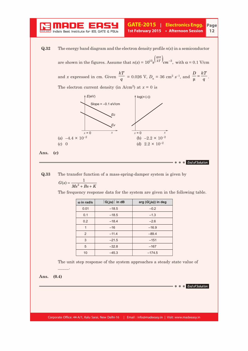
Q.32 The energy band diagram and the electron density profile n(x) in a semiconductor
are shown in the figures. Assume that n(x) = ⎛ ⎞⎜ ⎟⎝ ⎠ −
qaxkTe cm15 310 , with α = 0.1 V/cm
and x expressed in cm. Given kTq = 0.026 V, Dn = 36 cm2 s–1, and =
μD kT
q .
The electron current density (in A/cm2) at x = 0 is
Slope = –0.1 eV/cm
E(eV)
x = 0 x
Ec
Ev
x = 0 x
log( ( ))n x
(a) –4.4 × 10⁻² (b) –2.2 × 10⁻²
(c) 0 (d) 2.2 × 10⁻²
Ans. (c)
Q.33 The transfer function of a mass-spring-damper system is given by
=+ +
G sMs Bs K2
1( )
The frequency response data for the system are given in the following table.
in rad/s ⏐G( ) in dBj ⏐ arg ( ( )) in degG j
0.01 –18.5 –0.2
0.1 –18.5 –1.3
0.2 –18.4 –2.6
1 –16 –16.9
2 –11.4 –89.4
3 –21.5 –151
5 –32.8 –167
10 –45.3 –174.5
The unit step response of the system approaches a steady state value of_____.
Ans. (0.4)
Corporate Office: 44-A/1, Kalu Sarai, New Delhi-16 | Email : [email protected] | Visit: www.madeeasy.in
GATE-2015 | Electronics Engg.31st January 2015 • Afternoon Session
1234567890123456789012345678901234567890123456789012345678901234567890123456789012345678901234567890123456789012345678901234567890
Page13
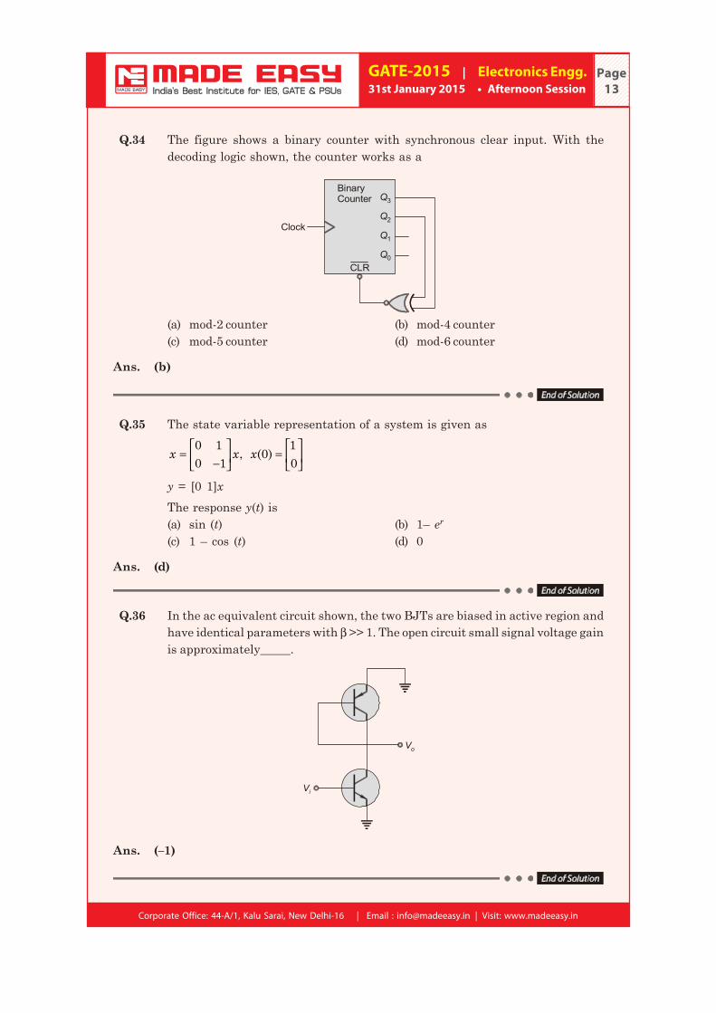
Q.34 The figure shows a binary counter with synchronous clear input. With thedecoding logic shown, the counter works as a
BinaryCounter Q3
Q2
Q1
Q0CLR
Clock
(a) mod-2 counter (b) mod-4 counter(c) mod-5 counter (d) mod-6 counter
Ans. (b)
Q.35 The state variable representation of a system is given as⎡ ⎤⎡ ⎤
= = ⎢ ⎥⎢ ⎥−⎣ ⎦ ⎣ ⎦x x x
0 1 1, (0)0 1 0
y = [0 1]xThe response y(t) is(a) sin (t) (b) 1– er
(c) 1 – cos (t) (d) 0
Ans. (d)
Q.36 In the ac equivalent circuit shown, the two BJTs are biased in active region andhave identical parameters with β >> 1. The open circuit small signal voltage gainis approximately_____.
Vo
Vi
Ans. (–1)

Corporate Office: 44-A/1, Kalu Sarai, New Delhi-16 | Email : [email protected] | Visit: www.madeeasy.in
GATE-2015 | Electronics Engg.1st February 2015 • Afternoon Session
1234567890123456789012345678901234567890123456789012345678901234567890123456789012345678901234567890123456789012345678901234567890
Page14
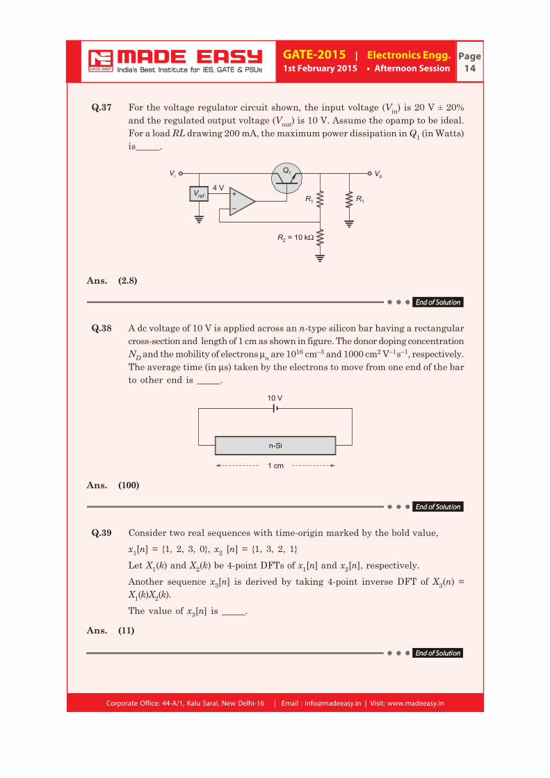
Q.37 For the voltage regulator circuit shown, the input voltage (Vin) is 20 V ± 20%and the regulated output voltage (Vout) is 10 V. Assume the opamp to be ideal.For a load RL drawing 200 mA, the maximum power dissipation in Q1 (in Watts)is_____.
+
–
Vi VoQ1
Vref4 V
R2 = 10 kΩ
R1 R1
Ans. (2.8)
Q.38 A dc voltage of 10 V is applied across an n-type silicon bar having a rectangularcross-section and length of 1 cm as shown in figure. The donor doping concentrationND and the mobility of electrons μn are 1016 cm–3 and 1000 cm2 V–1s–1, respectively.The average time (in μs) taken by the electrons to move from one end of the barto other end is _____.
n-Si
1 cm
10 V
Ans. (100)
Q.39 Consider two real sequences with time-origin marked by the bold value,x1[n] = {1, 2, 3, 0}, x2 [n] = {1, 3, 2, 1}Let X1(k) and X2(k) be 4-point DFTs of x1[n] and x2[n], respectively.Another sequence x3[n] is derived by taking 4-point inverse DFT of X3(n) =X1(k)X2(k).The value of x3[n] is _____.
Ans. (11)
Corporate Office: 44-A/1, Kalu Sarai, New Delhi-16 | Email : [email protected] | Visit: www.madeeasy.in
GATE-2015 | Electronics Engg.31st January 2015 • Afternoon Session
1234567890123456789012345678901234567890123456789012345678901234567890123456789012345678901234567890123456789012345678901234567890
Page15
Q.40 Input x(t) and output y(t) of an LTI system are related by the differential equationy″(t) – y′(t) –6y(t) = x(t). If the system is neither causal nor stable, the impulseresponse h(t) of the system is
(a) −− + −t te u t e u t3 21 1( ) ( )5 5
(b) −− − + −t te u t e u t3 21 1( ) ( )5 5
(c) −− −t te u t e u t3 21 1( ) ( )5 5
(d) −− − −t te u t e u t3 21 1( ) ( )5 5
Ans. (*)
Q.41 The value of the integral ∞
−∞
πππ∫ tt dtt
sin(4 )12cos(2 )4
is_____.
Ans. (3)
Q.42 Let x(t) = a s(t) + s(–t) with s(t) = βe–4tu(t), where u(t) is unit step function. Ifthe bilateral Laplace transform of x(t) is
= − < <−
X s ss2
16( ) 4 Re{ } 4;16
then the value of β is _____.
Ans. (–2)
Q.43 The electric field of a plane wave propagating in a lossless non-magnetic mediumis given by the following expression
E(z,t) = ax 5 cos (2π × 109t + βz) +ay 3 cos ππ × + β −9(2 10 t z )2
(a) Right Hand Circular (b) Left Hand Elliptical(c) Right Hand Elliptical (d) Linear
Ans. (b)
Q.44 Let X ∈ {0, 1} and Y ∈ {0, 1} be two independent binary random variables. IfP(X = 0) = p and P(Y = 0) = q, then P(X + Y ≥ 1) is equal to(a) pq (1 – p)(1 – q) (b) pq(c) p(1 – q) (d) 1 – pq
Ans. (d)
Corporate Office: 44-A/1, Kalu Sarai, New Delhi-16 | Email : [email protected] | Visit: www.madeeasy.in
GATE-2015 | Electronics Engg.1st February 2015 • Afternoon Session
1234567890123456789012345678901234567890123456789012345678901234567890123456789012345678901234567890123456789012345678901234567890
Page16
Q.45 If C denotes the counterclockwise unit circle, the value of the contour integral
π ∫�1 Re{ }2 c
z dzj
is _____.
Ans. (0)
Q.46 Consider a binary, digital communication system which uses pulses g(t) and –g(t) for transmitting bits over an AWGN channel. If the receiver uses a matchedfilter, which one of the following pulses will give the minimum probability of biterror?
(a)
1
1
g t( )
t
(b)
1
1
g t( )
t0
(c)
1
1
g t( )
t
(d)
1
1
g t( )
t0
Ans. (a)
Q.47 In the circuit shown, the initial voltages across the capacitors C1 and C2 and 1V and 3 V, respectively. The switch is closed at time t = 0. The total energydissipated (in Joules) in the resistor R until steady state is reached, is _____.
t = 0 R = 10 Ω
C1 = 3F+
–
+
–C2 = 3F
Ans. (3)
Corporate Office: 44-A/1, Kalu Sarai, New Delhi-16 | Email : [email protected] | Visit: www.madeeasy.in
GATE-2015 | Electronics Engg.31st January 2015 • Afternoon Session
1234567890123456789012345678901234567890123456789012345678901234567890123456789012345678901234567890123456789012345678901234567890
Page17
Q.48 The output of a standard second-order system for a unit step input is given as
y(t) = − π⎛ ⎞− −⎜ ⎟⎝ ⎠te t21 cos 3
63 . The transfer function of the system is
(a) + +s s2
( 2)( 3) (b)+ +s s2
12 1
(c)+ +s s2
32 3 (d)
+ +s s242 4
Ans. (d)
Q.49 Two half-wave dipole antennas placed as shown in the figure are excited withsinusoidally varying currents of frequency 3 MHz and phase shift of π/2 betweenthem (the element at the origin leads in phase). If the maximum radiated E-fieldat the point P in the x-y plane occurs at an azimuthal angle of 60°, the distanced (in meters) between the antennas is_____.
0
60°
z
d
x
yOP >> d
P
Ans. (50)
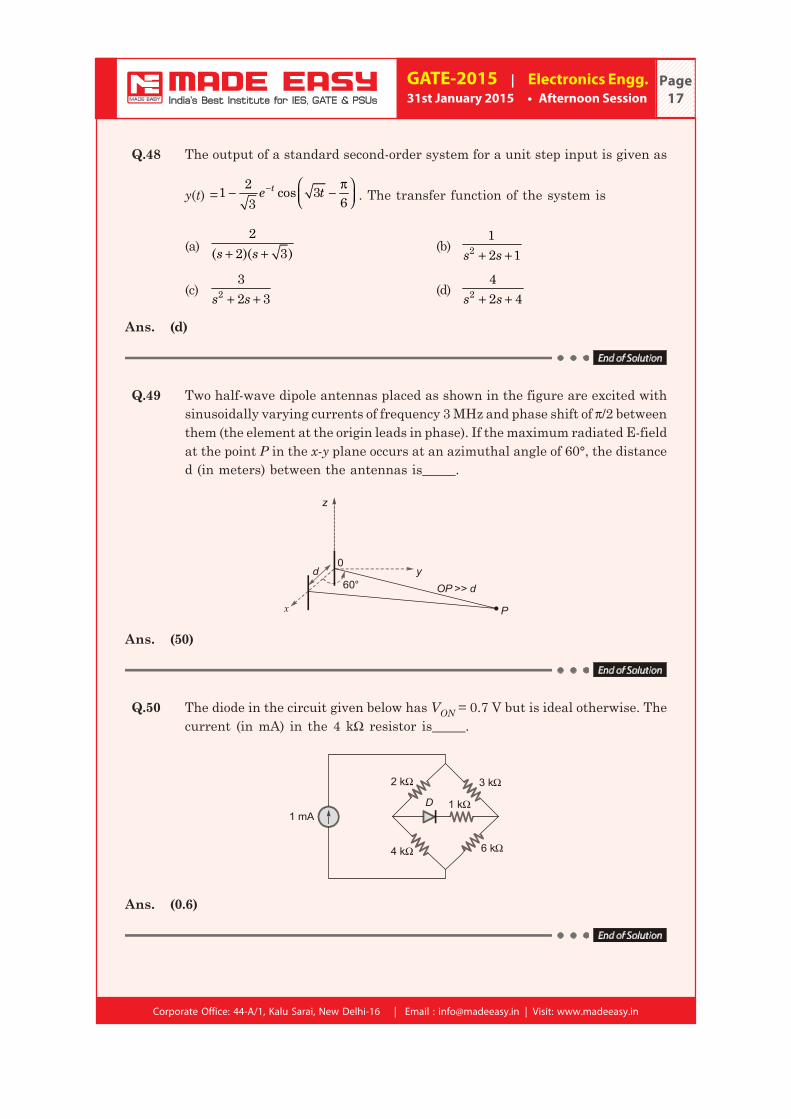
Q.50 The diode in the circuit given below has VON = 0.7 V but is ideal otherwise. Thecurrent (in mA) in the 4 kΩ resistor is_____.
3 kΩ
6 kΩ
2 kΩ
4 kΩ
1 kΩ1 mA
D
Ans. (0.6)
Corporate Office: 44-A/1, Kalu Sarai, New Delhi-16 | Email : [email protected] | Visit: www.madeeasy.in
GATE-2015 | Electronics Engg.1st February 2015 • Afternoon Session
1234567890123456789012345678901234567890123456789012345678901234567890123456789012345678901234567890123456789012345678901234567890
Page18
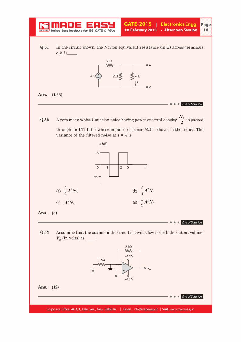
Q.51 In the circuit shown, the Norton equivalent resistance (in Ω) across terminalsa-b is_____.
a
b
+–
2 Ω
2 Ω 4 Ω4I
I
Ans. (1.33)
Q.52 A zero mean white Gaussian noise having power spectral density N02 is passed
through an LTI filter whose impulse response h(t) is shown in the figure. Thevariance of the filtered noise at t = 4 is
0 1 2 3
–A
h t( )
A
t
(a) A N20
32 (b) A N2
034
(c) A N20 (d) A N2
012
Ans. (a)
Q.53 Assuming that the opamp in the circuit shown below is deal, the output voltageV0 (in volts) is _____.
–
+
2 kΩ
1 kΩ
Vo
–12 V
–12 V
Ans. (12)
Corporate Office: 44-A/1, Kalu Sarai, New Delhi-16 | Email : [email protected] | Visit: www.madeeasy.in
GATE-2015 | Electronics Engg.31st January 2015 • Afternoon Session
1234567890123456789012345678901234567890123456789012345678901234567890123456789012345678901234567890123456789012345678901234567890
Page19
Q.54 Consider the differential equation = −dx xdt
10 0.2 with initial conduction x(0) = 1.
The response x(t) for t > 0 is(a) 2 –e–0.2t (b) 2 –e0.2t
(c) 50 –49e–0.2t (d) 50 –49e0.2t
Ans. (c)
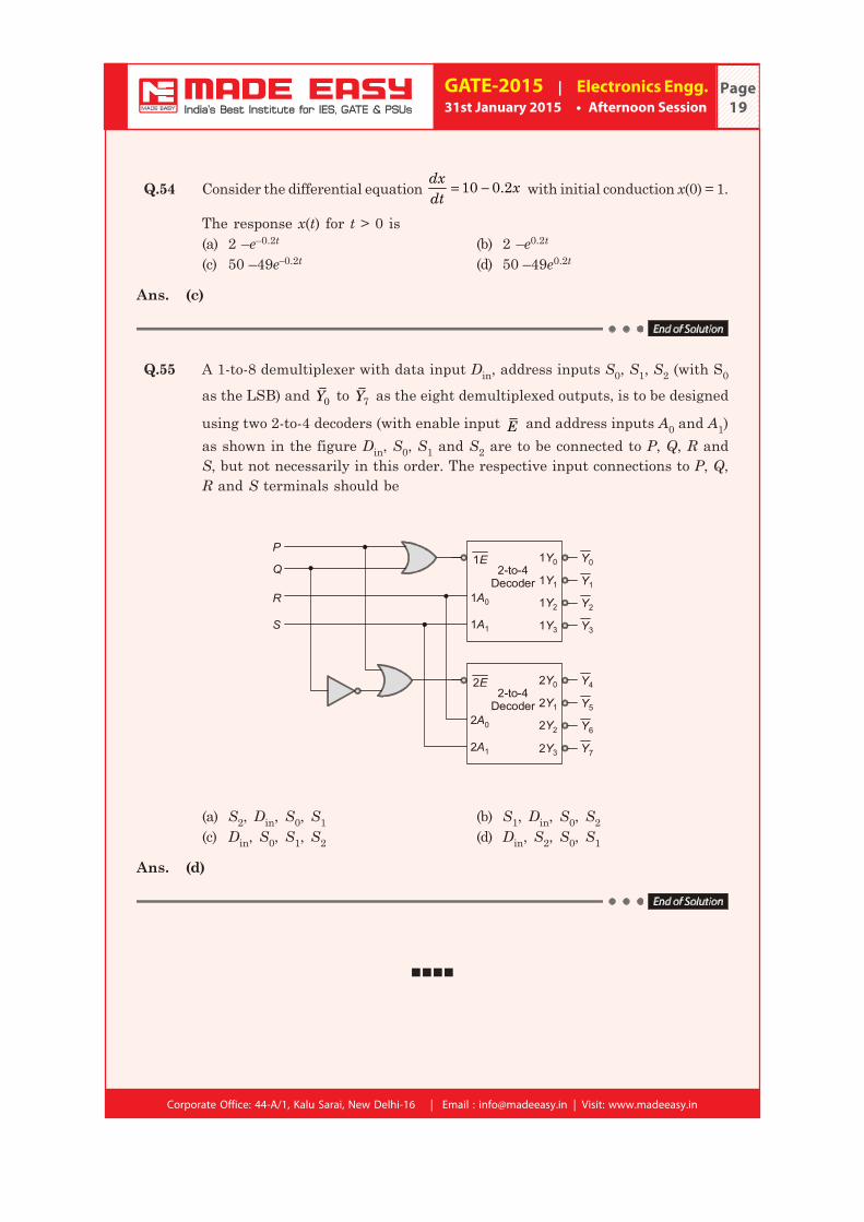
Q.55 A 1-to-8 demultiplexer with data input Din, address inputs S0, S1, S2 (with S0
as the LSB) and Y0 to Y7 as the eight demultiplexed outputs, is to be designed
using two 2-to-4 decoders (with enable input E and address inputs A0 and A1)as shown in the figure Din, S0, S1 and S2 are to be connected to P, Q, R andS, but not necessarily in this order. The respective input connections to P, Q,R and S terminals should be
1Y0 Y0
1Y1 Y1
1Y2 Y2
1Y3 Y3
1E2-to-4
Decoder1A0
1A1
2Y0 Y4
2Y1 Y5
2Y2 Y6
2Y3 Y7
2E2-to-4
Decoder2A0
2A1
P
Q
R
S
(a) S2, Din, S0, S1 (b) S1, Din, S0, S2(c) Din, S0, S1, S2 (d) Din, S2, S0, S1
Ans. (d)


![56]^ ‘a bcT !#$%&’()*+,-./01 23456789:;?@ABCDEjtt.hebei.gov.cn/res/jtyst/upload/file/20190313/e03f3a7032bc49c29cd724... · ’()*+,-./01(!"#!!"#$% &!!! """#$%&’ &()*+#,-./0](https://img.pdfslide.us/doc/110x75/5d573f6088c9934f278ba736/56-a-bct-01-23456789-01-.jpg)