Embed Size (px)
Citation preview

© 2009 - CATRENE – Report on Energy Autonomous Systems
1/84
CATRENE Working Group on Energy Autonomous Systems
Energy Autonomous Systems: Future Trends in Devices, Technology, and Systems
2 0 0 9 ‐ C A T R E N E ‐ C l u s t e r f o r A p p l i c a t i o n a n d T e c h n o l o g y R e s e a r c h i n E u r o p e o n N a n o e l e c t r o n i c s
© 2009 - CATRENE – Report on Energy Autonomous Systems
2/84
Energy Autonomous Systems: Future Trends in Devices, Technology, and Systems Contributors: Marc Belleville (CEA-LETI, France) Eugenio Cantatore (TU Eindhoven, The Netherlands) Herve Fanet (CEA-LETI, France) Paolo Fiorini (IMEC, Belgium) Pierre Nicole (THALES, France) Marcel Pelgrom (NXP, The Netherlands) Christian Piguet (CSEM, Switzerland) Robert Hahn (FhG, Germany) Chris Van Hoof (IMEC, Belgium) Ruud Vullers (IMEC-NL, The Netherlands) Marco Tartagni (University of Bologna, Italy), Coordinator <[email protected]> © 2009 - CATRENE http://www.catrene.org ISBN: 978-88-904-399-0-2 ISBN-A: 10.978.88904399/02
© 2009 - CATRENE – Report on Energy Autonomous Systems
3/84
Index
Index .............................................................................................................................................................................................. 3 Foreword ..................................................................................................................................................................................... 4 1. Introduction to Energy Autonomous Systems ........................................................................................................ 5 1.1. Definition of Energy Autonomous Systems ..................................................................................................... 5 1.2. Opportunities and applications of EAS .............................................................................................................. 6 1.3. Challenges of EAS and applications .................................................................................................................... 8
2. Current status of Energy Harvesting (EH) and Forward Look ...................................................................... 12 2.1. Science and Technology ........................................................................................................................................ 12 2.2. Commercial Exploitation ...................................................................................................................................... 21
3. Current Status of Energy Sources (ES) and Forward Look ............................................................................. 24 3.1. Science and Technology ........................................................................................................................................ 24 3.3. Commercial Exploitation ...................................................................................................................................... 30
4. Current Status of Ultra Low Power (ULP) Systems and Forward Look.................................................... 31 4.1. Science and Technology ........................................................................................................................................ 31 4.2. Commercial Exploitation ...................................................................................................................................... 47
5. Current status of Power Management (PM) and Forward Look .................................................................. 49 5.1. Science and Technology ........................................................................................................................................ 49 5.3. Commercial Exploitation ...................................................................................................................................... 56
6. European Situation and Forward Look ................................................................................................................... 58 6.1. Overview of Funding and Supporting Actions ............................................................................................ 58 6.2. Recommendations and Suggested Actions ................................................................................................... 63 6.3. Interdisciplinary Education and Training ..................................................................................................... 70
7. Bibliography ....................................................................................................................................................................... 75 7.1. Key Reports on EAS ................................................................................................................................................ 83 Acknowledgments ........................................................................................................................................................... 84

© 2009 - CATRENE – Report on Energy Autonomous Systems
4/84
Foreword
The rapid evolution of electronic devices since the beginning of the nanoelectronics era has brought about exceptional computational power in an ever shrinking system footprint. This has enabled among others the wealth of nomadic battery powered wireless systems (smart phones, mp3 players, GPS, …) that society currently enjoys. Emerging integration technologies enabling even smaller volumes and the associated increased functional density may bring about a new revolution in systems targeting wearable healthcare, wellness, lifestyle and industrial monitoring applications.
As systems continue to shrink, less energy is available on board which is creating a power challenge that prompts several important questions. What are the ultimate autonomy limits? Can systems be made completely energy autonomous? And if so, what are the ambient sources that could help enable such energy autonomy? Could on‐board intelligence allow greater net energy efficiency, despite its overhead in computational power?
Even though low‐cost batteries have been fostering the expansion towards nomadic systems, they
currently delay its further expansion as battery replacement or disposal is not an option in many of the envisaged applications and energy density is insufficient to achieve adequate autonomy. Although research towards higher energy‐density batteries is ongoing and new materials are revolutionizing the battery dimensions, their energy density does not scale accordingly.
To overcome this trend, another energy paradigm is needed and energy harvesting (also referred to
as energy scavenging) from the environment may provide a solution. A decade of research in the field of energy harvesting has led to the efficient capturing of small amounts of energy from the environment and transforming them into electrical energy. In parallel, suitable power management techniques are increasing the available energy budget, e.g. by dynamic optimization of voltage and clock rate, hybrid analog‐digital designs, and clever wake‐up procedures. Furthermore, advances in microprocessor technology have dramatically increased power efficiency, effectively reducing power consumption requirements. These developments together have stirred interest in new applications that rely entirely on energy harvesting for system power.
Energy autonomous systems using energy harvesting are particularly attractive when long‐term
remote deployment is needed or wherever a natural long‐term energy source is available (such as for example temperature or vibrations) for continuous replenishing of the energy consumed by the system. Such inexhaustible energy supply is a significant advantage over battery supply or mains powering. Extended lifetime and autonomy are also particularly advantageous in systems with limited accessibility, such as medical implants and infrastructure‐integrated micro‐sensors.
Based on the information collected during the study, specific recommendations and suggested
actions have been made on public initiatives, working methodology, and efficient research on a specific section of the report.
© 2009 - CATRENE – Report on Energy Autonomous Systems
5/84
1. Introduction to Energy Autonomous Systems
1.1. Definition of Energy Autonomous Systems
Energy Autonomous System: an electronic system that has been designed to operate and/or communicate as long as possible in known/unknown environments providing, elaborating and storing information without being connected to a power grid. The systems could operate in external natural or industrial environments as well as for in‐vivo applications in the diagnostic and therapeutic area. The power target should be particularly aggressive, and it is likely that several generations of prototypes will be necessary to achieve the goal to realize a system totally independent from the energy point of view. Regarding to the nowadays status‐of‐the‐art it will be referred to systems with ability to operate with less than hundreds of µW of power within less than some cubic centimeter. Examples of such systems are nomadic devices operating at ultra low power (wireless sensor networks, in‐vivo sentinels and actuators, ambient intelligence devices, “smart dust”). Cell phones or portable consumer electronics devices are not belonging, at the moment to this class.
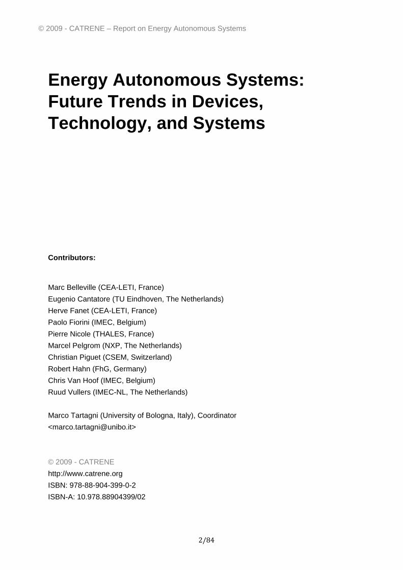
Energy Autonomous Systems could be roughly divided into three parts (Figure 1):
• Energy Generation, that consists of: o Energy Harvesting: Takes into account any device or system that could harvest
energy from correlated or uncorrelated sources of energy. It could consist of many techniques that can be classified by the type of energy used: temperature differences, light radiation, electromagnetic fields, kinetic energy, etc. The technique could take advantages of more sources at the same time.
o Energy Sources: this section takes into account any kind of energy storage element that could be used to accumulate energy in excess from the harvester and provide it to the system in its place whenever the energy is insufficient. Typically energy sources consist of electro‐chemical elements such as batteries or fuel cells or electrical storage systems such as capacitors.
• Energy Conversion and Optimization: this section is the trade of any energy conversion within the system and it has impact for two reasons. The first is that any source of harvesting energy should be disciplined with respect to the existing sources. The second point is that the energy used by intelligence should be less than what gained by the process itself.
• Energy Consumption: this is the section related to data acquisition, storage and transmission. This is of fundamental importance since most of the opportunities for energy harvesting are related to the efficiency of this part.
Figure 1: Structure of the Energy Autonomous Systems
© 2009 - CATRENE – Report on Energy Autonomous Systems
6/84
1.2. Opportunities and applications of EAS
The opportunities of EAS became increasingly interesting in the last five years due to the interactions of several key factors, more specifically, the decreasing computational energy, the increasing storage source capabilities and the energy conversions efficiency. However, the asymptotic energetic constraints of the system could be easily identified: the lower bound of computation is set by fundamental thermodynamic limit and the energy generation capability is restricted by several physical characteristics. Summarizing in few tips the key points of Energy Autonomous Systems:
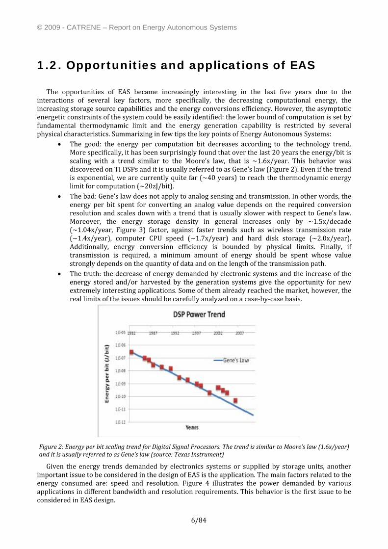
• The good: the energy per computation bit decreases according to the technology trend. More specifically, it has been surprisingly found that over the last 20 years the energy/bit is scaling with a trend similar to the Moore’s law, that is ~1.6x/year. This behavior was discovered on TI DSPs and it is usually referred to as Gene’s law (Figure 2). Even if the trend is exponential, we are currently quite far (~40 years) to reach the thermodynamic energy limit for computation (~20zJ/bit).
• The bad: Gene’s law does not apply to analog sensing and transmission. In other words, the energy per bit spent for converting an analog value depends on the required conversion resolution and scales down with a trend that is usually slower with respect to Gene’s law. Moreover, the energy storage density in general increases only by ~1.5x/decade (~1.04x/year, Figure 3) factor, against faster trends such as wireless transmission rate (~1.4x/year), computer CPU speed (~1.7x/year) and hard disk storage (~2.0x/year). Additionally, energy conversion efficiency is bounded by physical limits. Finally, if transmission is required, a minimum amount of energy should be spent whose value strongly depends on the quantity of data and on the length of the transmission path.
• The truth: the decrease of energy demanded by electronic systems and the increase of the energy stored and/or harvested by the generation systems give the opportunity for new extremely interesting applications. Some of them already reached the market, however, the real limits of the issues should be carefully analyzed on a case‐by‐case basis.
Figure 2: Energy per bit scaling trend for Digital Signal Processors. The trend is similar to Moore’s law (1.6x/year) and it is usually referred to as Gene’s law (source: Texas Instrument)
Given the energy trends demanded by electronics systems or supplied by storage units, another important issue to be considered in the design of EAS is the application. The main factors related to the energy consumed are: speed and resolution. Figure 4 illustrates the power demanded by various applications in different bandwidth and resolution requirements. This behavior is the first issue to be considered in EAS design.
© 2009 - CATRENE – Report on Energy Autonomous Systems
7/84
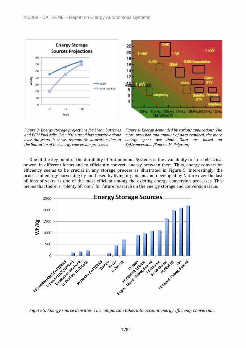
Figure 3: Energy storage projections for Liion batteries and PEM Fuel cells. Even if the trend has a positive slope over the years, it shows asymptotic saturation due to the limitation of the energy conversion processes.
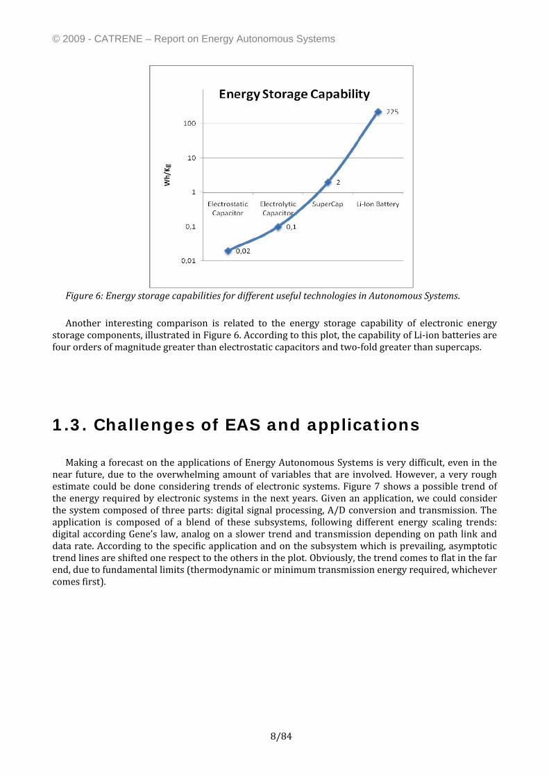
Figure 4: Energy demanded by various applications. The more precision and amount of data required, the more energy spent per time. Data are based on 5pJ/conversion. (Source: M. Pelgrom)
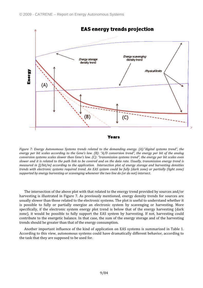
One of the key point of the durability of Autonomous Systems is the availability to store electrical power in different forms and to efficiently convert energy between them. Thus, energy conversion efficiency seems to be crucial in any storage process as illustrated in Figure 5. Interestingly, the process of energy harvesting by food used by living organisms and developed by Nature over the last billions of years, is one of the most efficient among the existing energy conversion processes. This means that there is “plenty of room” for future research on the energy storage and conversion issue.
Figure 5: Energy source densities. The comparison takes into account energy efficiency conversion.
© 2009 - CATRENE – Report on Energy Autonomous Systems
8/84
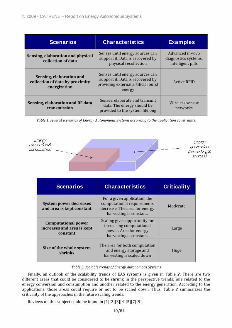
Figure 6: Energy storage capabilities for different useful technologies in Autonomous Systems. Another interesting comparison is related to the energy storage capability of electronic energy
storage components, illustrated in Figure 6. According to this plot, the capability of Li‐ion batteries are four orders of magnitude greater than electrostatic capacitors and two‐fold greater than supercaps.
1.3. Challenges of EAS and applications
Making a forecast on the applications of Energy Autonomous Systems is very difficult, even in the near future, due to the overwhelming amount of variables that are involved. However, a very rough estimate could be done considering trends of electronic systems. Figure 7 shows a possible trend of the energy required by electronic systems in the next years. Given an application, we could consider the system composed of three parts: digital signal processing, A/D conversion and transmission. The application is composed of a blend of these subsystems, following different energy scaling trends: digital according Gene’s law, analog on a slower trend and transmission depending on path link and data rate. According to the specific application and on the subsystem which is prevailing, asymptotic trend lines are shifted one respect to the others in the plot. Obviously, the trend comes to flat in the far end, due to fundamental limits (thermodynamic or minimum transmission energy required, whichever comes first).
© 2009 - CATRENE – Report on Energy Autonomous Systems
9/84
Figure 7: Energy Autonomous Systems trends related to the demanding energy. (A):”digital systems trend”, the energy per bit scales according to the Gene’s law. (B): “A/D conversion trend”, the energy per bit of the analog conversion systems scales slower than Gene’s law. (C): “transmission systems trend”, the energy per bit scales even slower and it is related to the path link to be covered and on the data rate. Usually, transmission energy trend is measured in [J/bit/m] according to the application. Intersection plot of energy storage and harvesting densities trends with electronic systems required trend. An EAS system could be fully (dark zone) or partially (light zone) supported by energy harvesting or scavenging whenever the two line do (or do not) intersect.
The intersection of the above plot with that related to the energy trend provided by sources and/or harvesting is illustrated in Figure 7. As previously mentioned, energy density trends for sources are usually slower than those related to the electronic systems. The plot is useful to understand whether it is possible to fully or partially energize an electronic system by scavenging or harvesting. More specifically, if the electronic system energy plot trend is below that of the energy harvesting (dark zone), it would be possible to fully support the EAS system by harvesting. If not, harvesting could contribute to the energetic balance. In that case, the sum of the energy storage and of the harvesting trends should be greater than that of the energy consumption.
Another important influence of the kind of application on EAS systems is summarized in Table 1. According to this view, autonomous systems could have dramatically different behavior, according to the task that they are supposed to be used for.
© 2009 - CATRENE – Report on Energy Autonomous Systems
10/84
Scenarios Characteristics Examples
Sensing, elaboration and physical collection of data
Senses until energy sources can support it. Data is recovered by
physical recollection
Advanced in‐vivo diagnostics systems, intelligent pills
Sensing, elaboration and collection of data by proximity
energization
Senses until energy sources can support it. Data is recovered by providing external artificial burst
energy
Active RFID
Sensing, elaboration and RF data transmission
Senses, elaborate and transmit data. The energy should be
provided to the system lifelong
Wireless sensor networks
Table 1: several scenarios of Energy Autonomous Systems according to the application constraints.
Scenarios Characteristics Criticality
System power decreases and area is kept constant
For a given application, the computational requirements decrease. The area for energy
harvesting is constant.
Moderate
Computational power increases and area is kept
constant
Scaling gives opportunity for increasing computational power. Area for energy harvesting is constant.
Large
Size of the whole system shrinks
The area for both computation and energy storage and harvesting is scaled down
Huge
Table 2: scalable trends of Energy Autonomous Systems
Finally, an outlook of the scalability trends of EAS systems is given in Table 2. There are two different areas that could be considered to be shrunk in the perspective trends: one related to the energy conversion and consumption and another related to the energy generation. According to the applications, those areas could require or not to be scaled down. Thus, Table 2 summarizes the criticality of the approaches in the future scaling trends.
Reviews on this subject could be found in [1][2][3][4][5][7][9].
© 2009 - CATRENE – Report on Energy Autonomous Systems
11/84
Energy Autonomous Systems may contribute to many applications in different sectors. Among them portable autonomous systems could open new endemic scenarios for:
• wireless sensor networks (e.g. environmental monitoring in production plants, humanized environments, agriculture, etc.)
• wireless security systems ( e.g. ad‐hoc networking in harsh environments) • in situ monitoring for mobile/moving systems (e.g. tire pressure monitoring systems,
industrial process control ) • body area networks (e.g. health monitoring, active clothing, wearable energy sources,
pervasive electronics) • biomedical devices (e.g. pacemakers, continuous biological parameters monitoring systems,
in‐situ drug delivery) • portable power generation for mobile electronics.
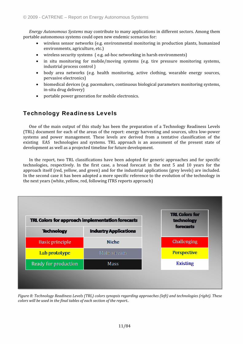
Technology Readiness Levels One of the main output of this study has been the preparation of a Technology Readiness Levels
(TRL) document for each of the areas of the report: energy harvesting and sources, ultra low‐power systems and power management. These levels are derived from a tentative classification of the existing EAS technologies and systems. TRL approach is an assessment of the present state of development as well as a projected timeline for future development.
In the report, two TRL classifications have been adopted for generic approaches and for specific
technologies, respectively. In the first case, a broad forecast in the next 5 and 10 years for the approach itself (red, yellow, and green) and for the industrial applications (grey levels) are included. In the second case it has been adopted a more specific reference to the evolution of the technology in the next years (white, yellow, red, following ITRS reports approach)
Figure 8: Technology Readiness Levels (TRL) colors synopsis regarding approaches (left) and technologies (right). Thesecolors will be used in the final tables of each section of the report..
© 2009 - CATRENE – Report on Energy Autonomous Systems
12/84
2. Current status of Energy Harvesting (EH) and Forward Look
2.1. Science and Technology
Energy harvesting or scavenging is the conversion of ambient energy into electrical energy, by means of a specific transduction principle. Vibration, heat or solar energy are the main sources of ambient energy. In a strict definition, harvesting makes use of ambient energy which is not released on purpose and otherwise would be lost. However, in this report a broader definition is used: Also the case where energy is released with the purpose of feeding remote harvesting devices will be discussed. An example of the latter case is the conversion of RF energy which is transmitted by a designated emitting device.
2.1.1. Harvesting Principles In this section we briefly describe the physical principles on which harvesting of vibrational,
thermal, photovoltaic and RF energy is based. More specifically, various extended reviews exist on energy harvesting from human body [4][5] and environment [6][7][8][9].
A. Vibrational harvesting
A vibration harvester is typically composed of a frame anchored to the vibration source and a mass m connected to the frame by a suspension having a stiffness k. The vibration induces a relative motion of the mass and the frame, a transducer transform the energy of this relative motion into electricity.
The main characteristic of a vibration energy harvester is that it operates in resonance. The resonance frequency is given by:
mkf
π=21
The power in resonance for a mass‐spring system is given by [7]:
max334)( YzmffP π=
where Y is the external vibration amplitude and zmax the maximum displacement of the proof mass, limited by the dimensions of the frame. It follows from the above equation that large output powers are enabled by higher vibration frequencies.
There are three ways of converting vibration into energy • Electrostatic (ES): A capacitor is made consisting of two opposing metal structures. One
of these structures is fixed, the other one moves in presence of an external force. The change in voltage is proportional to the capacitance change
• Piezoelectric (PE): A mass is suspended by a beam, with a piezo electric layer on top of the beam. When the mass starts to vibrate, the piezoelectric layer is deformed and a voltage is generated
• Electromagnetic or Inductive (EM): A mass of magnetic material moves through a magnetic field. The change in flux generates a voltage.
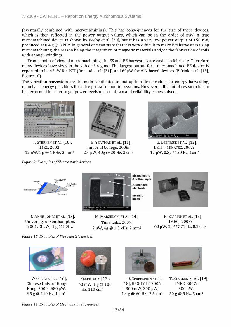
In the figures below, some of the published results are shown for Electrostatic (Figure 9), Piezoelectric (Figure 10) and Electromagnetic (Figure 11) harvesting devices. One can clearly differentiate between the ES and PE on one hand, and on the EM on the other hand. The latter ones are rarely completely micromachined, most of the time macroscopic fabrication techniques are used
© 2009 - CATRENE – Report on Energy Autonomous Systems
13/84
(eventually combined with micromachining). This has consequences for the size of these devices, which is then reflected in the power output values, which can be in the order of mW. A true micromachined device is shown by Beeby et al. [20], but it has a very low power output of 150 nW, produced at 0.4 g @ 8 kHz. In general one can state that it is very difficult to make EM harvesters using micromachining, the reason being the integration of magnetic materials and/or the fabrication of coils with enough windings.
From a point of view of micromachining, the ES and PE harvesters are easier to fabricate. Therefore many devices have sizes in the sub cm2 regime. The largest output for a micromachined PE device is reported to be 45µW for PZT (Renaud et al. [21]) and 60µW for AlN based devices (Elfrink et al. [15], Figure 10). The vibration harvesters are the main candidates to end up in a first product for energy harvesting, namely as energy providers for a tire pressure monitor systems. However, still a lot of research has to be performed in order to get power levels up, cost down and reliability issues solved.
WEN J. LI ET AL. [16], Chinese Univ. of Hong Kong, 2000: 680 µW, 95 g @ 110 Hz, 1 cm3
PERPETUUM [17], 40 mW, 1 g @ 100 Hz, 110 cm3
D. SPREEMANN ET AL. [18], HSG‐IMIT, 2006:300 mW, 300 µW,
1.4 g @ 60 Hz, 2.5 cm3
T. STERKEN ET AL. [19], IMEC, 2007: 300 µW,
50 g @ 5 Hz, 5 cm3
Figure 10: Examples of Piezoelectric devices
GLYNNE‐JONES ET AL. [13], University of Southampton, 2001: 3 µW, 1 g @ 80Hz
M. MARZENCKI ET AL [14], Tima Labs, 2007:
2 µW, 4g @ 1.3 kHz, 2 mm2
R. ELFRINK ET AL. [15],IMEC, 2008:
60 µW, 2g @ 571 Hz, 0.2 cm2
Figure 9: Examples of Electrostatic devices
T. STERKEN ET AL. [10], IMEC, 2003:
12 nW, 1 g @ 1 kHz, 2 mm3
E. YEATMAN ET AL. [11],Imperial College, 2006:
2.4 µW, 40g @ 20 Hz, 3 cm2
G. DESPESSE ET AL. [12],LETI – MINATEC, 2007:
12 µW, 0.3g @ 50 Hz, 1cm2
Figure 11: Examples of Electromagnetic devices
© 2009 - CATRENE – Report on Energy Autonomous Systems
14/84
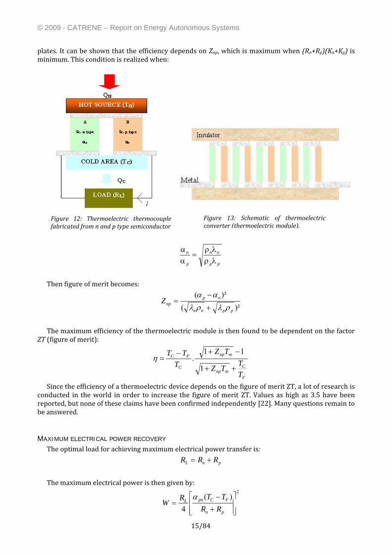
B. Thermal harvesting
In the case of thermal harvesting, two effects can be deployed. Using the Seebeck effect, one makes use of a spatial temperature difference. Another option is using a pyrolectric element, which can turn a temporal temperature difference into electricity. Since the efficiency of the latter is very low, only the first effect will be considered.
Thermal energy harvesters are based on the Seebeck effect. Their core element is a thermopile, formed by a large number of thermocouples placed between a hot and a cold plate. The thermocouples are thermally connected in parallel and electrically in series. The generator may include a radiator for efficient dissipation of heat in the ambient and specific structures aimed to increase thermal isolation between the hot and cold plate.
THE SEEBECK EFFECT The Seebeck effect is associated with the generation of a voltage along a conductor when it is
subjected to a temperature difference. Charged carriers (electrons or holes) diffuse from the hot side to the cold side, creating an internal electric field that opposes further diffusion. The Seebeck coefficient is defined as the voltage generated per degree of temperature difference between two points. In practice, the measurement of the potential difference drifting of the Seebeck electric field requires the use of a second driver to carry out the contact with the Voltmeter, which leads to the direct measurement of the difference of the Seebeck coefficients of two materials concerned:
( )( )chBA TTV −α−α−=Δ ,
where ΔV is the observed potential difference (in Volts), and αi the Seebeck coefficients of materials A and B (in V/K) respectively, and (Th – Tc) the temperature difference between the hot source and the cold source (in Kelvin). This equation is valid if the variation in temperature is sufficiently weak to be able to neglect the dependence in temperature of the Seebeck coefficient.
EFFICIENCY OF A THERMOGENERATOR By considering the simplest generators consisting of a single thermocouple with thermo elements
fabricated from n and p type semiconductors (Figure 12), the efficiency of the generator is given by:
HQW
=η
Assuming constant electrical conductivity, thermal conductivity and Seebeck coefficient in the thermoelectric couple and negligible contact resistances, then the electrical power is given by:
²IRW L= and the current I is:
Lpn
CHpn
RRRTT
I++
−=
)(α
We now define Znp, which is the figure of merit of the n/p couple,
))((²
pnpn
pnnp KKRR
Z++
=α
A thermoelectric converter (usually referred to as a module) is shown schematically in Figure 13. It
consists of n‐type and p type semiconductor thermo‐elements connected electrically in series by highly conducting metal strips and sandwiched between thermally conducting (electrically insulating)
© 2009 - CATRENE – Report on Energy Autonomous Systems
15/84
plates. It can be shown that the efficiency depends on Znp, which is maximum when (Rn+Rp)(Kn+Kp) is minimum. This condition is realized when:
pp
nn
p
n
λρλρ
=αα
Then figure of merit becomes:
)²()²(
ppnn
npnpZ
ρλρλαα
+
−=
The maximum efficiency of the thermoelectric module is then found to be dependent on the factor
ZT (figure of merit):
F
Cmnp
mnp
C
FC
TTTZ
TZT
TT
++
−+−=
1
11.η
Since the efficiency of a thermoelectric device depends on the figure of merit ZT, a lot of research is conducted in the world in order to increase the figure of merit ZT. Values as high as 3.5 have been reported, but none of these claims have been confirmed independently [22]. Many questions remain to be answered.
MAXIMUM ELECTRICAL POWER RECOVERY The optimal load for achieving maximum electrical power transfer is:
pnL RRR +=
The maximum electrical power is then given by:
2)(
4 ⎥⎥⎦
⎤
⎢⎢⎣
⎡
+
−=
pn
FCpnL
RRTTRW
α
Figure 13: Schematic of thermoelectricconverter (thermoelectric module).
Figure 12: Thermoelectric thermocouplefabricated from n and p type semiconductor
© 2009 - CATRENE – Report on Energy Autonomous Systems
16/84
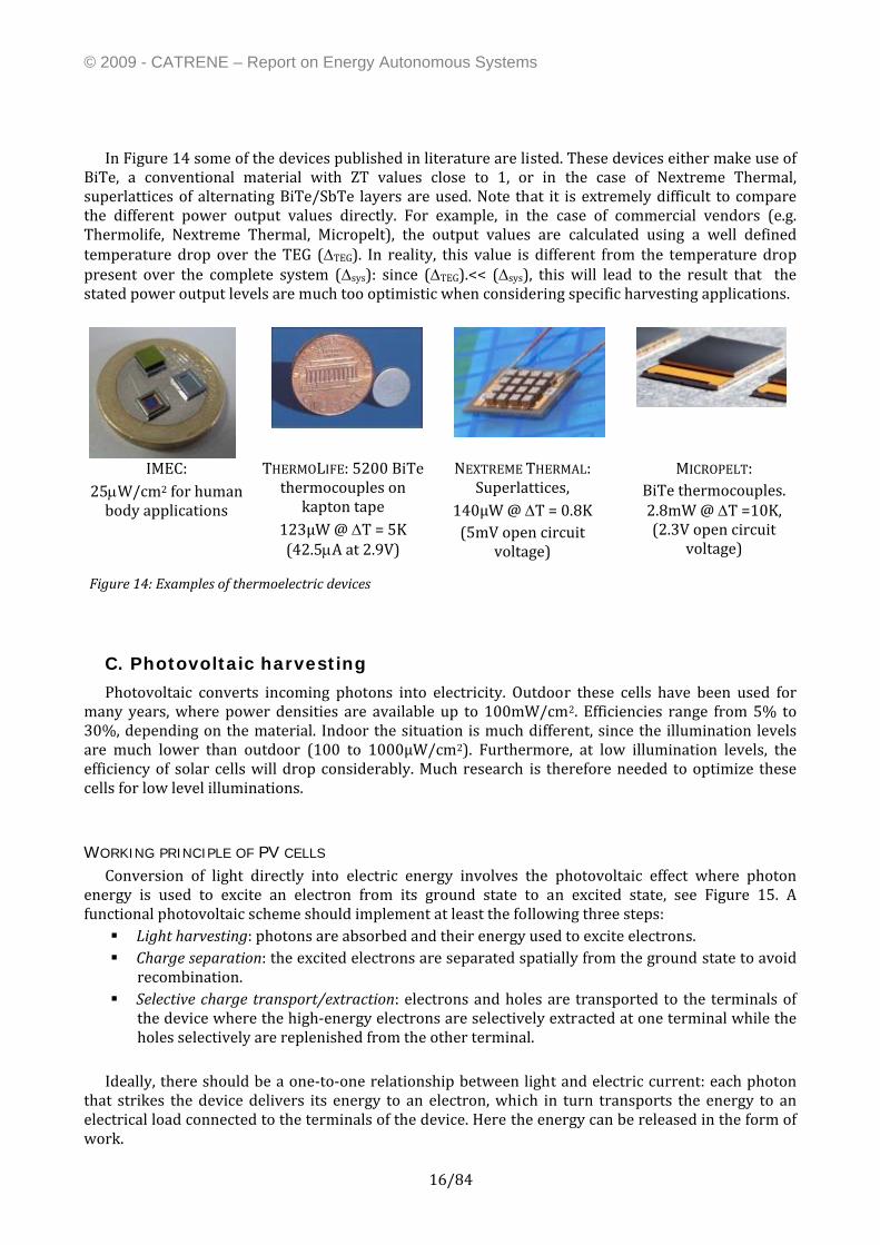
In Figure 14 some of the devices published in literature are listed. These devices either make use of
BiTe, a conventional material with ZT values close to 1, or in the case of Nextreme Thermal, superlattices of alternating BiTe/SbTe layers are used. Note that it is extremely difficult to compare the different power output values directly. For example, in the case of commercial vendors (e.g. Thermolife, Nextreme Thermal, Micropelt), the output values are calculated using a well defined temperature drop over the TEG (ΔTEG). In reality, this value is different from the temperature drop present over the complete system (Δsys): since (ΔTEG).<< (Δsys), this will lead to the result that the stated power output levels are much too optimistic when considering specific harvesting applications.
C. Photovoltaic harvesting
Photovoltaic converts incoming photons into electricity. Outdoor these cells have been used for many years, where power densities are available up to 100mW/cm2. Efficiencies range from 5% to 30%, depending on the material. Indoor the situation is much different, since the illumination levels are much lower than outdoor (100 to 1000µW/cm2). Furthermore, at low illumination levels, the efficiency of solar cells will drop considerably. Much research is therefore needed to optimize these cells for low level illuminations.
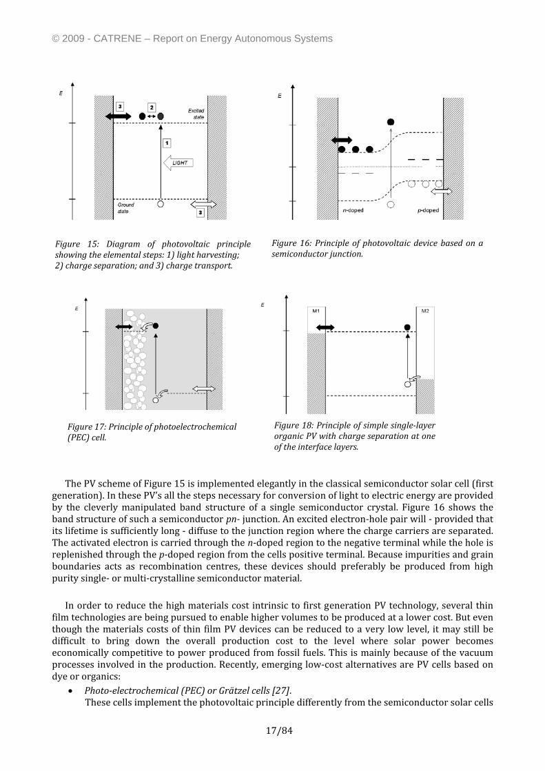
WORKING PRINCIPLE OF PV CELLS Conversion of light directly into electric energy involves the photovoltaic effect where photon
energy is used to excite an electron from its ground state to an excited state, see Figure 15. A functional photovoltaic scheme should implement at least the following three steps:
Light harvesting: photons are absorbed and their energy used to excite electrons. Charge separation: the excited electrons are separated spatially from the ground state to avoid recombination.
Selective charge transport/extraction: electrons and holes are transported to the terminals of the device where the high‐energy electrons are selectively extracted at one terminal while the holes selectively are replenished from the other terminal.
Ideally, there should be a one‐to‐one relationship between light and electric current: each photon
that strikes the device delivers its energy to an electron, which in turn transports the energy to an electrical load connected to the terminals of the device. Here the energy can be released in the form of work.
IMEC: 25μW/cm2 for human body applications
THERMOLIFE: 5200 BiTe thermocouples on
kapton tape 123µW @ ΔT = 5K (42.5μA at 2.9V)
NEXTREME THERMAL:Superlattices,
140µW @ ΔT = 0.8K (5mV open circuit
voltage)
MICROPELT: BiTe thermocouples. 2.8mW @ ΔT =10K, (2.3V open circuit
voltage)
Figure 14: Examples of thermoelectric devices
© 2009 - CATRENE – Report on Energy Autonomous Systems
17/84
The PV scheme of Figure 15 is implemented elegantly in the classical semiconductor solar cell (first generation). In these PV’s all the steps necessary for conversion of light to electric energy are provided by the cleverly manipulated band structure of a single semiconductor crystal. Figure 16 shows the band structure of such a semiconductor pn junction. An excited electron‐hole pair will ‐ provided that its lifetime is sufficiently long ‐ diffuse to the junction region where the charge carriers are separated. The activated electron is carried through the ndoped region to the negative terminal while the hole is replenished through the pdoped region from the cells positive terminal. Because impurities and grain boundaries acts as recombination centres, these devices should preferably be produced from high purity single‐ or multi‐crystalline semiconductor material.
In order to reduce the high materials cost intrinsic to first generation PV technology, several thin
film technologies are being pursued to enable higher volumes to be produced at a lower cost. But even though the materials costs of thin film PV devices can be reduced to a very low level, it may still be difficult to bring down the overall production cost to the level where solar power becomes economically competitive to power produced from fossil fuels. This is mainly because of the vacuum processes involved in the production. Recently, emerging low‐cost alternatives are PV cells based on dye or organics:
• Photoelectrochemical (PEC) or Grätzel cells [27]. These cells implement the photovoltaic principle differently from the semiconductor solar cells
Figure 18: Principle of simple singlelayer organic PV with charge separation at one of the interface layers.
Figure 17: Principle of photoelectrochemical (PEC) cell.
Figure 16: Principle of photovoltaic device based on asemiconductor junction.
Figure 15: Diagram of photovoltaic principleshowing the elemental steps: 1) light harvesting; 2) charge separation; and 3) charge transport.
© 2009 - CATRENE – Report on Energy Autonomous Systems
18/84
– see Figure 17. Light absorption occurs in a transition metal complex (dye) that is absorbed on the inner surface of a nano‐particulate, porous layer of anatase (titanium dioxide, a white pigment used in paints and tooth paste). The excited electron is immediately transferred to the conduction band of the anatase, and the remaining electron vacancy is replenished from a liquid or solid redox electrolyte.
• OrganicBased Photovoltaics.
Recently, substantial advances have been achieved in the conversion efficiencies of PV’s based on molecular (organic) semiconductors and on conducting polymers [28]. In these organic‐based PV’s, excitons play an important role. Excitons are mobile, electrically neutral, optically excited states, which exist because they do not have enough energy to separate into an electron and a hole – in other words: the optical band gap is smaller than the electrical band gap. In organic materials this is often because charge separation involves a conformation change and thus requires a relatively large energy (Figure 18). Nanowires or quantum dot like absorber materials are used to validate the proof of concept of the nanotechnologies. The main objectives of this will be to decrease the manufacturing cost
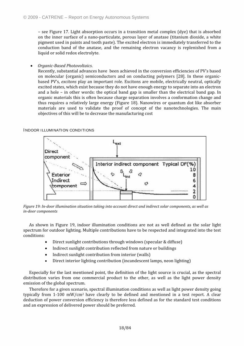
INDOOR ILLUMINATION CONDITIONS
Figure 19: Indoor illumination situation taking into account direct and indirect solar components, as well as indoor components
As shown in Figure 19, indoor illumination conditions are not as well defined as the solar light
spectrum for outdoor lighting. Multiple contributions have to be respected and integrated into the test conditions:
• Direct sunlight contributions through windows (specular & diffuse) • Indirect sunlight contribution reflected from nature or buildings • Indirect sunlight contribution from interior (walls) • Direct interior lighting contribution (incandescent lamps, neon lighting)
Especially for the last mentioned point, the definition of the light source is crucial, as the spectral
distribution varies from one commercial product to the other, as well as the light power density emission of the global spectrum.
Therefore for a given scenario, spectral illumination conditions as well as light power density going typically from 1‐100 mW/cm2 have clearly to be defined and mentioned in a test report. A clear deduction of power conversion efficiency is therefore less defined as for the standard test conditions and an expression of delivered power should be preferred.
© 2009 - CATRENE – Report on Energy Autonomous Systems
19/84
Standard Test Conditions are defined by using a AM1.5G solar spectrum, 100 mW/cm2 light intensity and 25 °C device temperature. The definition of an AM spectrum is as follows:
• AM: Air Mass AM=(P/P0)*(1/sinθ), with P: local pressure, P0: 1013 mbar, θ: Angle between the direct solar light vector and the horizontal surface.
• AM0: Solar spectrum without atmosphere interaction • AM1: Solar spectrum with normal incidence • AM1.5: Solar spectrum on a 37° tilted surface (for average sun trajectory) • AM1.5G: as AM1.5 taking into account direct and diffuse lighting
IDENTIFYING IN-DOOR PV TECHNOLOGIES Solar cell comparison is generally based on an arbitrary maximum terrestrial intensity and spectra
(of 1 sun, 1000 W/m2) at 25°C perpendicular to the cell plane referred to by specialists as AM1.5. In practice, no solar cell experiences such conditions, yet few alternative bases for comparison exist [29]. Given that the indoor photovoltaic devices, when compared with the outdoor solar cells, are characterised by much lower radiant energy intensities, various spectra (including artificial light sources), complete comparison data for indoor conditions are not freely available.
The inexorable growth in low power micro‐electronic devices such as sensors and MEMS is an opportunity for increasing the use of PV especially for indoor applications. Photovoltaic modules may be used to partially or completely source the energy required for the functioning of such systems. For information, indoor consumer PV represented 4 MWP in 1997. It is of note that the 1 sun efficiency reference of such statistics is misleading for indoor products, as electrical efficiency is much less important indoors. This is because the end‐user decision to purchase an indoor PV (IPV) product is not related to the solar cell electrical efficiency but rather to such benefits as reduced reliance on batteries (”plug and forget”) and increased reliability i.e. a correctly designed and used IPV system can run longer without user intervention than when powered by batteries alone. From an environmental responsibility perspective, reducing battery waste is also laudable.
Using semi‐conductor materials for the development of in‐door photovoltaic devices leads rapidly to the use of direct band‐gap materials. In fact, the low irradiance conditions (0.01 – 0.1 sun) creates charge generating and transport mechanism condition, that in‐direct semiconductor materials like crystalline silicon are suffering of significant energy conversion losses.
D. RF Harvesting
RF harvesting converts electromagnetic radiation into electricity. This can be done in two ways. • Make use of existing EM radiation (e.g. GSM, FM, WiFi) • Broadcast an EM signal at a specific wavelength in order to power a wireless node. The first solution has the advantage that radiation can be used that is already present. The
disadvantage is the low energy density (typically µW/cm2). Furthermore, it is not always desirable or even legal to block radiation (e.g. for emergency calls). Therefore, a solution is to use dedicated broadcasting device, which can power sensors in the neighborhood. A point of concern is the maximum power that is allowed to be transmitted into the environment, which is typically around 100mW.
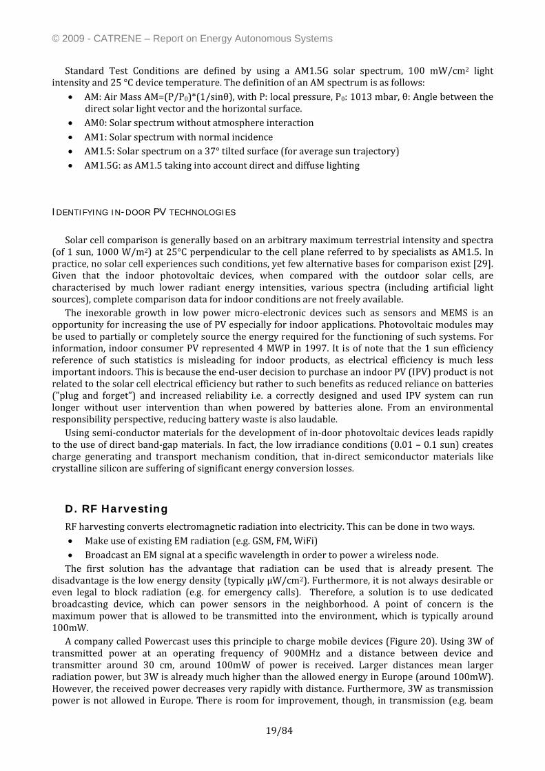
A company called Powercast uses this principle to charge mobile devices (Figure 20). Using 3W of transmitted power at an operating frequency of 900MHz and a distance between device and transmitter around 30 cm, around 100mW of power is received. Larger distances mean larger radiation power, but 3W is already much higher than the allowed energy in Europe (around 100mW). However, the received power decreases very rapidly with distance. Furthermore, 3W as transmission power is not allowed in Europe. There is room for improvement, though, in transmission (e.g. beam
© 2009 - CATRENE – Report on Energy Autonomous Systems
20/84
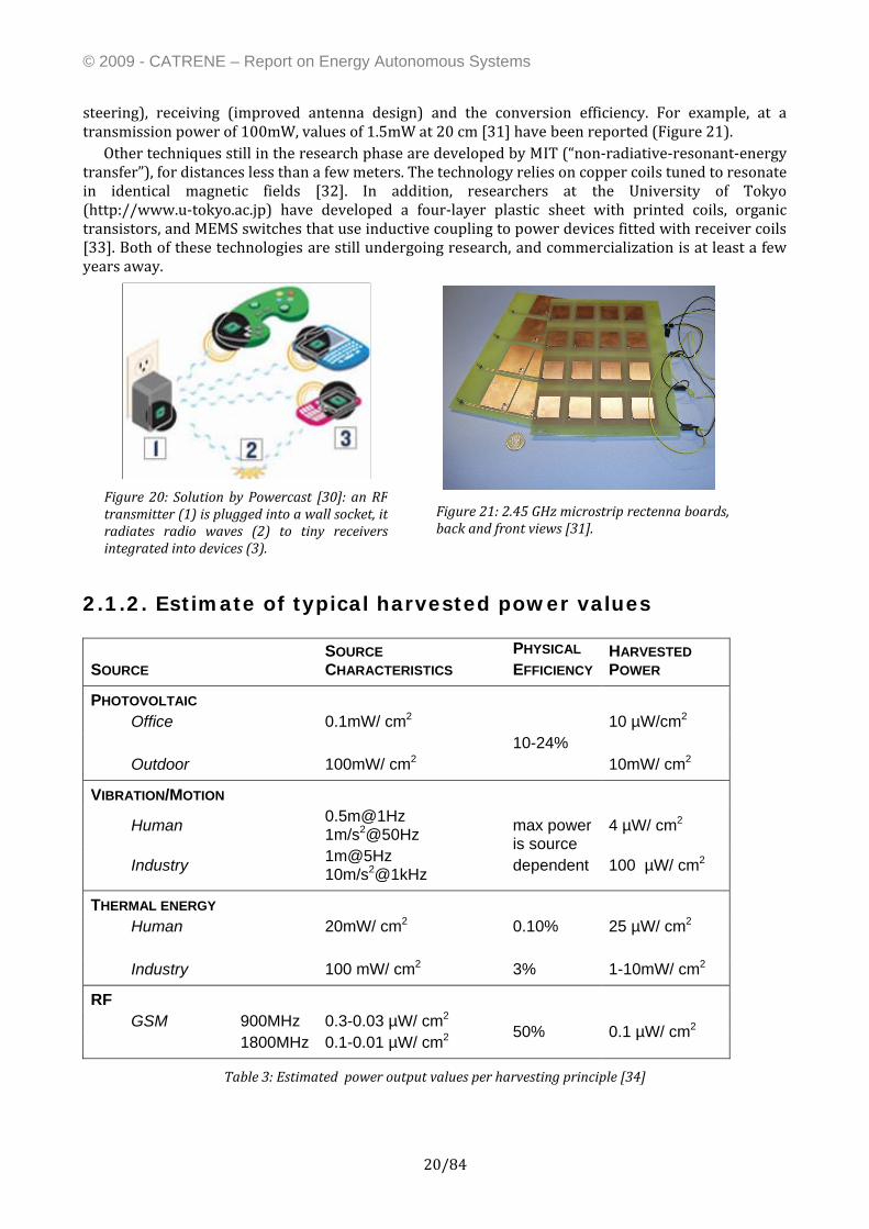
steering), receiving (improved antenna design) and the conversion efficiency. For example, at a transmission power of 100mW, values of 1.5mW at 20 cm [31] have been reported (Figure 21).
Other techniques still in the research phase are developed by MIT (“non‐radiative‐resonant‐energy transfer”), for distances less than a few meters. The technology relies on copper coils tuned to resonate in identical magnetic fields [32]. In addition, researchers at the University of Tokyo (http://www.u‐tokyo.ac.jp) have developed a four‐layer plastic sheet with printed coils, organic transistors, and MEMS switches that use inductive coupling to power devices fitted with receiver coils [33]. Both of these technologies are still undergoing research, and commercialization is at least a few years away.
2.1.2. Estimate of typical harvested power values
SOURCE SOURCE CHARACTERISTICS
PHYSICAL EFFICIENCY
HARVESTED POWER
PHOTOVOLTAIC Office 0.1mW/ cm2 10 µW/cm2 10-24% Outdoor 100mW/ cm2 10mW/ cm2
VIBRATION/MOTION
Human 0.5m@1Hz 1m/s2@50Hz max power
is source dependent
4 µW/ cm2
Industry 1m@5Hz 10m/s2@1kHz 100 µW/ cm2
THERMAL ENERGY Human 20mW/ cm2 0.10% 25 µW/ cm2 Industry 100 mW/ cm2 3% 1-10mW/ cm2
RF GSM 900MHz 0.3-0.03 µW/ cm2
50% 0.1 µW/ cm2 1800MHz 0.1-0.01 µW/ cm2
Table 3: Estimated power output values per harvesting principle [34]
Figure 21: 2.45 GHz microstrip rectenna boards, back and front views [31].
Figure 20: Solution by Powercast [30]: an RFtransmitter (1) is plugged into a wall socket, itradiates radio waves (2) to tiny receiversintegrated into devices (3).
© 2009 - CATRENE – Report on Energy Autonomous Systems
21/84
In Table 3 the estimated figures of energy output values per harvesting principle are listed (from [34]). Note that these numbers are just first order indications, and they have to be considered to have a large error margin. However, they do give some indication of the typical expected power levels.
2.2. Commercial Exploitation
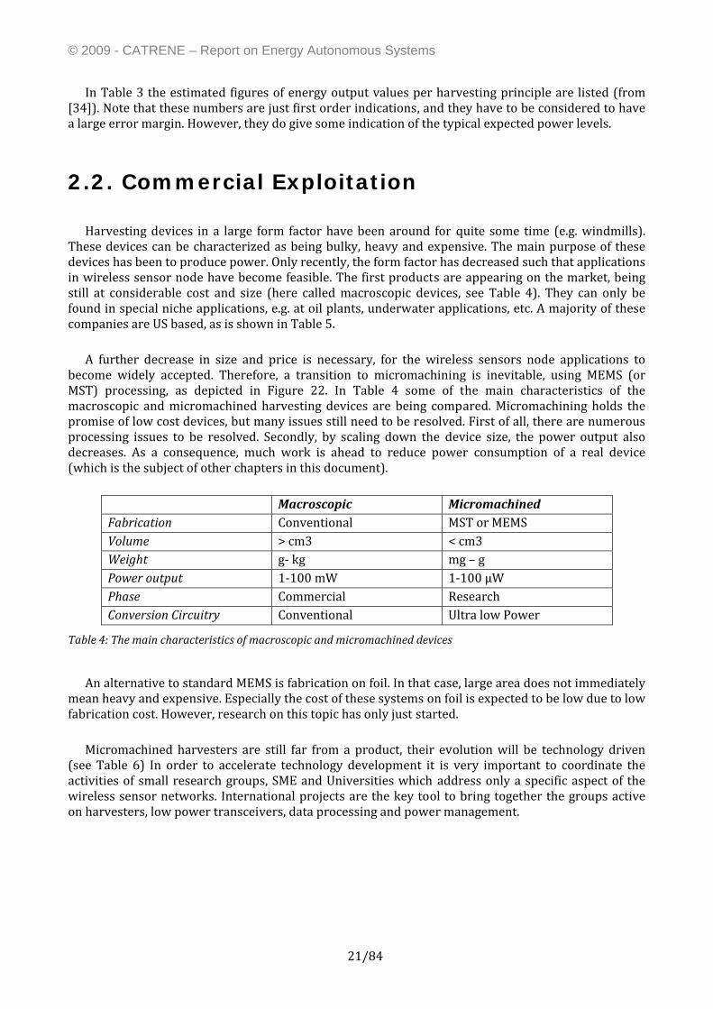
Harvesting devices in a large form factor have been around for quite some time (e.g. windmills). These devices can be characterized as being bulky, heavy and expensive. The main purpose of these devices has been to produce power. Only recently, the form factor has decreased such that applications in wireless sensor node have become feasible. The first products are appearing on the market, being still at considerable cost and size (here called macroscopic devices, see Table 4). They can only be found in special niche applications, e.g. at oil plants, underwater applications, etc. A majority of these companies are US based, as is shown in Table 5.
A further decrease in size and price is necessary, for the wireless sensors node applications to
become widely accepted. Therefore, a transition to micromachining is inevitable, using MEMS (or MST) processing, as depicted in Figure 22. In Table 4 some of the main characteristics of the macroscopic and micromachined harvesting devices are being compared. Micromachining holds the promise of low cost devices, but many issues still need to be resolved. First of all, there are numerous processing issues to be resolved. Secondly, by scaling down the device size, the power output also decreases. As a consequence, much work is ahead to reduce power consumption of a real device (which is the subject of other chapters in this document).
Macroscopic Micromachined Fabrication Conventional MST or MEMS Volume > cm3 < cm3 Weight g‐ kg mg – g Power output 1‐100 mW 1‐100 µW Phase Commercial Research Conversion Circuitry Conventional Ultra low Power
Table 4: The main characteristics of macroscopic and micromachined devices
An alternative to standard MEMS is fabrication on foil. In that case, large area does not immediately mean heavy and expensive. Especially the cost of these systems on foil is expected to be low due to low fabrication cost. However, research on this topic has only just started.
Micromachined harvesters are still far from a product, their evolution will be technology driven
(see Table 6) In order to accelerate technology development it is very important to coordinate the activities of small research groups, SME and Universities which address only a specific aspect of the wireless sensor networks. International projects are the key tool to bring together the groups active on harvesters, low power transceivers, data processing and power management.
© 2009 - CATRENE – Report on Energy Autonomous Systems
22/84
Figure 22: The transition from macro to micromachining will cause a decrease in device size, as well as output power.
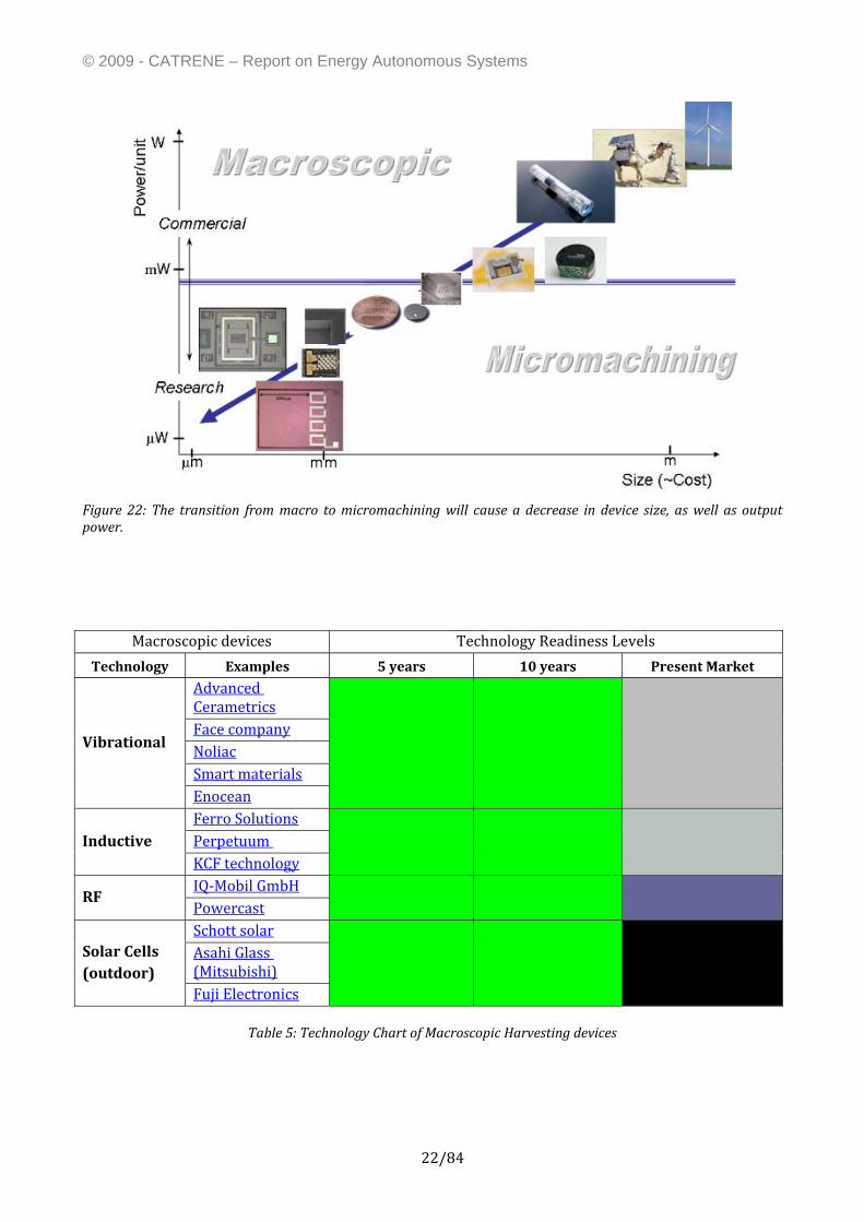
Macroscopic devices Technology Readiness Levels Technology Examples 5 years 10 years Present Market
Vibrational
Advanced Cerametrics
Face company Noliac Smart materials Enocean
Inductive Ferro Solutions
Perpetuum KCF technology
RF IQ‐Mobil GmbH
Powercast
Solar Cells (outdoor)
Schott solar
Asahi Glass (Mitsubishi) Fuji Electronics
Table 5: Technology Chart of Macroscopic Harvesting devices
© 2009 - CATRENE – Report on Energy Autonomous Systems
23/84
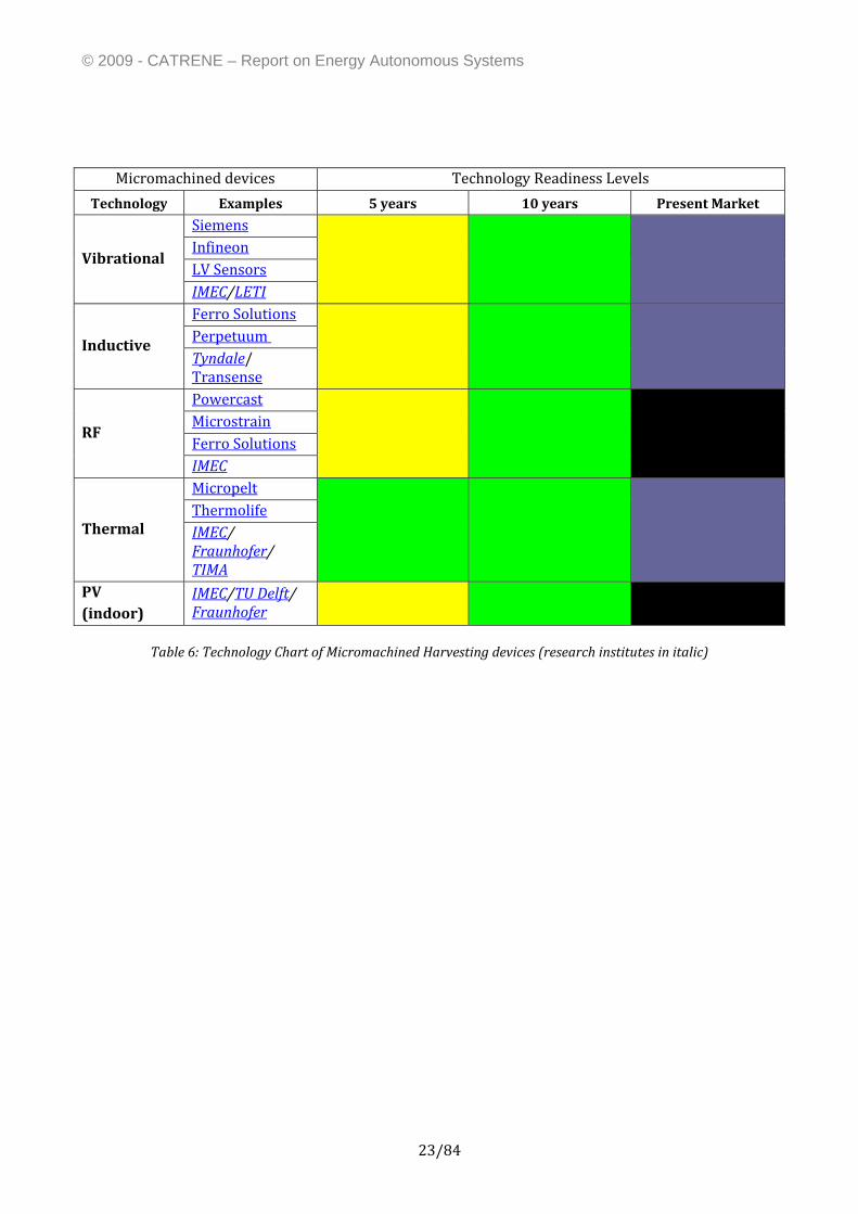
Micromachined devices Technology Readiness Levels Technology Examples 5 years 10 years Present Market
Vibrational
Siemens
Infineon LV Sensors IMEC/LETI
Inductive
Ferro Solutions
Perpetuum Tyndale/ Transense
RF
Powercast
Microstrain Ferro Solutions IMEC
Thermal
Micropelt
Thermolife IMEC/ Fraunhofer/ TIMA
PV (indoor)
IMEC/TU Delft/ Fraunhofer
Table 6: Technology Chart of Micromachined Harvesting devices (research institutes in italic)
© 2009 - CATRENE – Report on Energy Autonomous Systems
24/84
3. Current Status of Energy Sources (ES) and Forward Look
3.1. Science and Technology
3.1.1. Science and Technology of micro battery technology, especially as buffer storage for energy harvesting devices
Effective intermediate energy storage is required for all energy harvesting concepts, due to the varying availability of ambient energy and varying energy requirements of the device. In most cases this intermediate storage is best done with the help of a secondary micro battery. Secondary batteries have a much higher energy density compared to capacitors and sufficient power pulse capability.
Thus, the development of miniaturized power sources, with high volumetric energy density, is of crucial importance for small electronic applications like small sensor nodes, active smart labels or MEMS.
The energy density of batteries decreases rapidly by reducing the size of the batteries. This is caused by the increasing amount of passive packaging material in proportion to active material in small batteries. There is a significant reduction of energy density at a thickness of below 1 mm because the volume of the packaging foil becomes dominant.
Several approaches have been described for the development of micro batteries. At Oak Ridge
National Laboratory a process has been created in which a secondary thin‐film lithium battery can be deposited onto a chip [35]. The thickness of the entire battery is in the order of 100’s of µm’s and the areas studied are in the cm² range. This battery is a layered structure with alternate layers of lithium manganese oxide (or lithium cobalt oxide), lithium phosphate oxynitride and lithium metal. The maximum cell voltage is 4.2 V at max. current output in the order of 1 mA/cm² and 5 mA/cm² for the LiCoO2 ‐ Lithium based cell respectively. All layers are fabricated using vacuum processing. The deposition of the electrolyte layer is a particularly highly sophisticated and time consuming process that leads to high production costs. Electrical cycling of the solid‐state battery leads to cyclic changes of crystallite volume and material tension. Therefore, the total capacity is rather low since layer thickness cannot be increased above a few micrometers.
Another way of miniaturization was developed by downsizing the technology for laser welded metal casings and glass feed through technology [36]. Since this battery has a cylindrical format, integration and interconnection is not straight forward. Costs of these batteries as well as thin film batteries is very high which prevents utilization in the mass marked.
A three‐dimensional battery assembly process [37] was developed whereby battery materials are filled into high aspect ratio holes of a substrate such as glass or silicon. Although the capacity per substrate area is rather high (up to 2 mAh/cm²), volumetric energy density is not more than approx. 80 Wh/l. While batteries according to approach [35] and [36] are already on the market, this technology is still in academic stage.
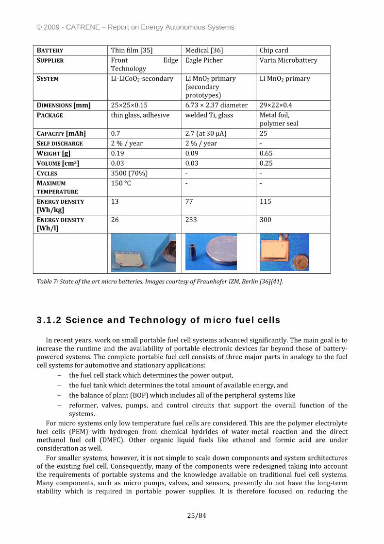
Table 7 gives an exemplary overview of the existing battery technologies. It can be seen, that the energy density of micro batteries is far below that of standard Li‐polymer (200 Wh/kg, 400 Wh/l) batteries which are used for example in mobile phones.
© 2009 - CATRENE – Report on Energy Autonomous Systems
25/84
BATTERY Thin film [35] Medical [36] Chip card SUPPLIER Front Edge
Technology Eagle Picher Varta Microbattery
SYSTEM Li‐LiCoO2‐secondary Li MnO2 primary (secondary prototypes)
Li MnO2 primary
DIMENSIONS [mm] 25×25×0.15 6.73 × 2.37 diameter 29×22×0.4 PACKAGE thin glass, adhesive welded Ti, glass Metal foil,
polymer seal CAPACITY [mAh] 0.7 2.7 (at 30 µA) 25 SELF DISCHARGE 2 % / year 2 % / year ‐ WEIGHT [g] 0.19 0.09 0.65 VOLUME [cm3] 0.03 0.03 0.25 CYCLES 3500 (70%) ‐ ‐ MAXIMUM TEMPERATURE
150 °C ‐ ‐
ENERGY DENSITY [Wh/kg]
13 77 115
ENERGY DENSITY [Wh/l]
26 233 300
Table 7: State of the art micro batteries. Images courtesy of Fraunhofer IZM, Berlin [36][41].
3.1.2 Science and Technology of micro fuel cells In recent years, work on small portable fuel cell systems advanced significantly. The main goal is to
increase the runtime and the availability of portable electronic devices far beyond those of battery‐powered systems. The complete portable fuel cell consists of three major parts in analogy to the fuel cell systems for automotive and stationary applications:
− the fuel cell stack which determines the power output, − the fuel tank which determines the total amount of available energy, and − the balance of plant (BOP) which includes all of the peripheral systems like − reformer, valves, pumps, and control circuits that support the overall function of the
systems. For micro systems only low temperature fuel cells are considered. This are the polymer electrolyte
fuel cells (PEM) with hydrogen from chemical hydrides of water‐metal reaction and the direct methanol fuel cell (DMFC). Other organic liquid fuels like ethanol and formic acid are under consideration as well.
For smaller systems, however, it is not simple to scale down components and system architectures of the existing fuel cell. Consequently, many of the components were redesigned taking into account the requirements of portable systems and the knowledge available on traditional fuel cell systems. Many components, such as micro pumps, valves, and sensors, presently do not have the long‐term stability which is required in portable power supplies. It is therefore focused on reducing the
© 2009 - CATRENE – Report on Energy Autonomous Systems
26/84
peripheral components and building the so‐called “passive systems”. Thus, costs and volume can be reduced and reliability increased.
Comparison of Li-ion batteries and portable fuel cells
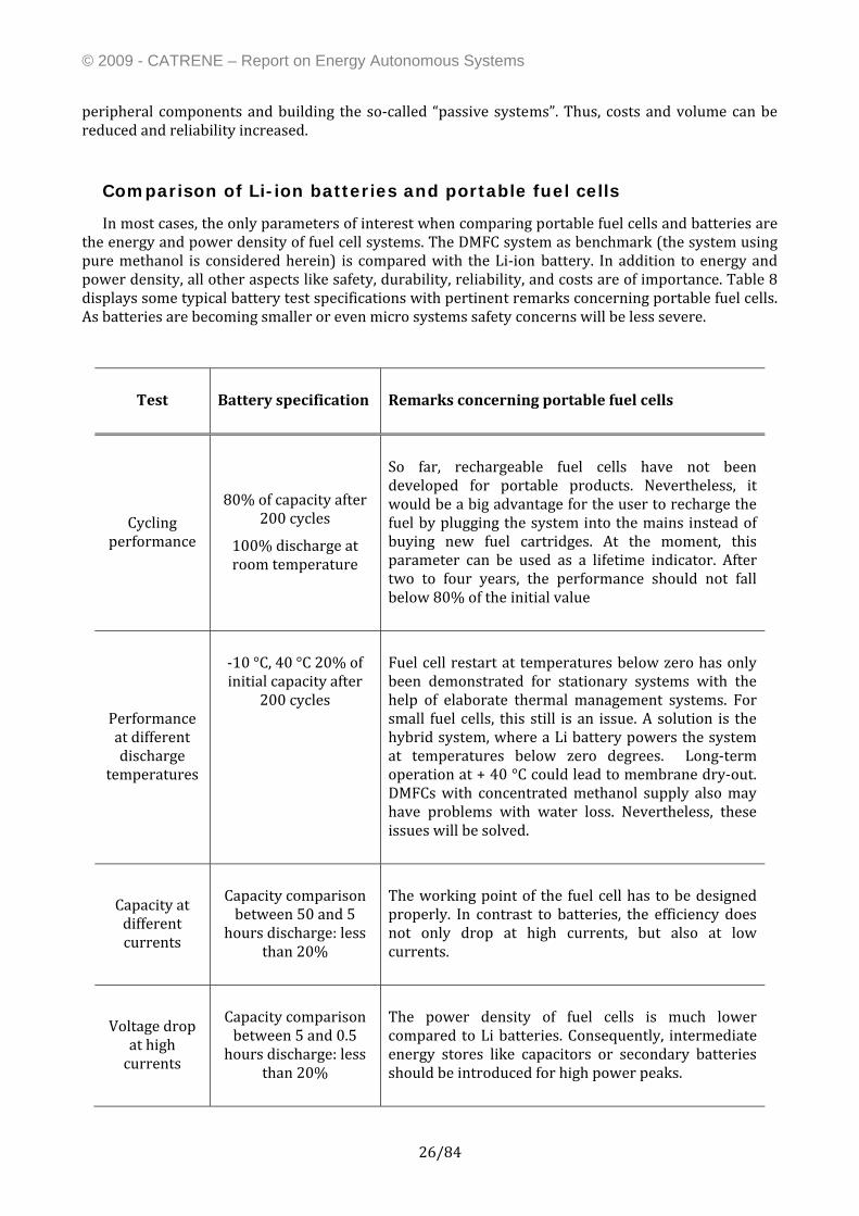
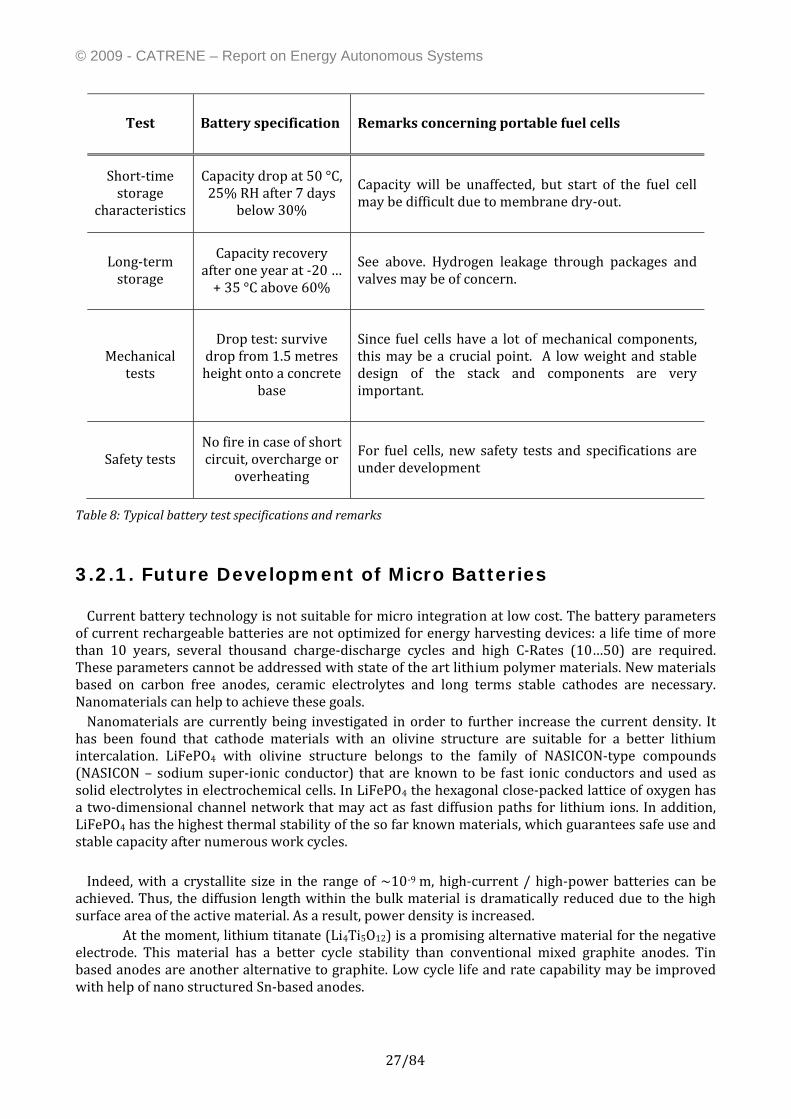
In most cases, the only parameters of interest when comparing portable fuel cells and batteries are the energy and power density of fuel cell systems. The DMFC system as benchmark (the system using pure methanol is considered herein) is compared with the Li‐ion battery. In addition to energy and power density, all other aspects like safety, durability, reliability, and costs are of importance. Table 8 displays some typical battery test specifications with pertinent remarks concerning portable fuel cells. As batteries are becoming smaller or even micro systems safety concerns will be less severe.
Test Battery specification
Remarks concerning portable fuel cells
Cycling performance
80% of capacity after 200 cycles
100% discharge at room temperature
So far, rechargeable fuel cells have not been developed for portable products. Nevertheless, it would be a big advantage for the user to recharge the fuel by plugging the system into the mains instead of buying new fuel cartridges. At the moment, this parameter can be used as a lifetime indicator. After two to four years, the performance should not fall below 80% of the initial value
Performance at different discharge
temperatures
‐10 °C, 40 °C 20% of initial capacity after
200 cycles
Fuel cell restart at temperatures below zero has only been demonstrated for stationary systems with the help of elaborate thermal management systems. For small fuel cells, this still is an issue. A solution is the hybrid system, where a Li battery powers the system at temperatures below zero degrees. Long‐term operation at + 40 °C could lead to membrane dry‐out. DMFCs with concentrated methanol supply also may have problems with water loss. Nevertheless, these issues will be solved.
Capacity at different currents
Capacity comparison between 50 and 5
hours discharge: less than 20%
The working point of the fuel cell has to be designed properly. In contrast to batteries, the efficiency does not only drop at high currents, but also at low currents.
Voltage drop at high currents
Capacity comparison between 5 and 0.5 hours discharge: less
than 20%
The power density of fuel cells is much lower compared to Li batteries. Consequently, intermediate energy stores like capacitors or secondary batteries should be introduced for high power peaks.
© 2009 - CATRENE – Report on Energy Autonomous Systems
27/84
Test
Battery specification
Remarks concerning portable fuel cells
Short‐time storage
characteristics
Capacity drop at 50 °C, 25% RH after 7 days
below 30%
Capacity will be unaffected, but start of the fuel cell may be difficult due to membrane dry‐out.
Long‐term storage
Capacity recovery after one year at ‐20 … + 35 °C above 60%
See above. Hydrogen leakage through packages and valves may be of concern.
Mechanical tests
Drop test: survive drop from 1.5 metres height onto a concrete
base
Since fuel cells have a lot of mechanical components, this may be a crucial point. A low weight and stable design of the stack and components are very important.
Safety tests No fire in case of short circuit, overcharge or
overheating
For fuel cells, new safety tests and specifications are under development
Table 8: Typical battery test specifications and remarks
3.2.1. Future Development of Micro Batteries Current battery technology is not suitable for micro integration at low cost. The battery parameters
of current rechargeable batteries are not optimized for energy harvesting devices: a life time of more than 10 years, several thousand charge‐discharge cycles and high C‐Rates (10…50) are required. These parameters cannot be addressed with state of the art lithium polymer materials. New materials based on carbon free anodes, ceramic electrolytes and long terms stable cathodes are necessary. Nanomaterials can help to achieve these goals. Nanomaterials are currently being investigated in order to further increase the current density. It
has been found that cathode materials with an olivine structure are suitable for a better lithium intercalation. LiFePO4 with olivine structure belongs to the family of NASICON‐type compounds (NASICON – sodium super‐ionic conductor) that are known to be fast ionic conductors and used as solid electrolytes in electrochemical cells. In LiFePO4 the hexagonal close‐packed lattice of oxygen has a two‐dimensional channel network that may act as fast diffusion paths for lithium ions. In addition, LiFePO4 has the highest thermal stability of the so far known materials, which guarantees safe use and stable capacity after numerous work cycles. Indeed, with a crystallite size in the range of ~10‐9 m, high‐current / high‐power batteries can be
achieved. Thus, the diffusion length within the bulk material is dramatically reduced due to the high surface area of the active material. As a result, power density is increased. At the moment, lithium titanate (Li4Ti5O12) is a promising alternative material for the negative
electrode. This material has a better cycle stability than conventional mixed graphite anodes. Tin based anodes are another alternative to graphite. Low cycle life and rate capability may be improved with help of nano structured Sn‐based anodes.

© 2009 - CATRENE – Report on Energy Autonomous Systems
28/84
Optimized active materials, such as nanoparticles of Li4Ti5O12 with olivine structures as cathode intercalation matrix, can be used to reduce the bulk diffusion and, hence, increase the ability to operate at high current peaks. Additional performance improvement may be realized through the use of 3‐D architectures. This is
especially convenient for micro scale batteries since Lithography and technologies adapted from Si and MEMS processing can be used. The use of the vertical dimension enables the battery to have a small areal footprint. Power density can be improved due to short ion diffusion length and high surface area. Special crystal growth and vacuum deposition technologies, which will never be scalable for large
batteries can be used to increase the performance of micro batteries. This may be carbon nano tubes or nano sized silicon columns for improved conductivity and Li intercalation [42]. Substrate integration of micro batteries is an important practical issue [38]. In case of wafer‐level batteries where battery laminates can be assembled in cavities of silicon
wafers to use the silicon substrate as an MEMS hermetic package. Battery laminates from Li‐polymer mass production can be used for this technology. Thus, costs are relatively low. In mass production usually a laminated foil package is used and liquid electrolyte is dispensed
before encapsulation. The liquid electrolyte is not easy to handle and will degrade the sealing surfaces of a micro battery. In addition, the high vapor pressure of the battery prevents the use of vacuum technology for encapsulation. Therefore a gel type electrolyte would be required which is compatible to the active masses of the secondary battery. All materials and processes have to be optimized for ultra low water content and ultra low humidity and gas permeation. Typical specifications are as follows:
High energy density (> 300 Wh/l) High pulse discharge rate (> 10 C) small geometrical dimensions and flexible form factors (down to 1 mm2, 200 µm thickness), minor self‐discharge high cycle stability of up to 10000 cycles long life of 10 years and more in some cases high temperature stability.
3.2.3. Future Developments of Micro Fuel Cells A significant research effort is to miniaturise the fuel cells. Special improvement is required for the
balance of plant by using miniaturised and high‐reliability components and more passively working fuel cell technologies. Especially, water management is a crucial part of any fuel cell system and is particularly challenging to miniaturise. For small units, MEMS pumps and valves probably will have to be developed. While the first components appear on the market, a huge effort is still needed to increase the reliability, reduce their own energy consumption, and the costs.
The use of micro technologies for the fuel cell core is aimed at reaching two objectives:

© 2009 - CATRENE – Report on Energy Autonomous Systems
29/84
− The specific fuel cell performance may be significantly improved when micro scaling processes are used. Fuel cells built to investigate micro‐scale phenomena are smaller, use the volume more efficiently, and improve heat and mass transfer. Therefore, problems critical in conventional stack technology may be solved by the micro technological design of the three‐phase boundary, the development of ultra‐thin ion‐conducting membranes, the fabrication of transport‐optimised flow channels on the micro scale, the introduction of nanomaterials, and others. Most of these aspects are interdependent and have to be investigated and designed simultaneously. For example, ultra‐thin electrolytes require the presence of narrow support structures in the micrometre range that may impede the flow of reactants.
− The majority of research activities related to micro‐scale fuel cells is also aimed at micro‐power applications. There are many new miniaturised applications which can only be implemented, if a higher‐energy‐density power source is available compared to button cells and other small batteries. Miniaturisation of the conventional fuel cell stack technology is not possible down to these dimensions.
While PEM micro fuel cell can be regarded as relatively mature and the research focus is on
hydrogen supply, the liquid fuel cells like DMFC and DEFC still suffer from a lot of problems. Most critical are:
The slow reaction rate and thus low power Poisoning from reaction intermediates Fuel cross over and Material degradation of catalysts, three phase boundary and ion membrane. A significant amount of materials research is required to tackle theses issues.
Another direction of research will be directed towards energy autarkic micro fuel cells which
derive their fuel from the surrounding ambient. Two basic principles can be distinguished: 1. Autarkic fuel generators which are producing the fuel for the fuel cell separately. This may be
hydrogen, generated from electrochemical corrosion of metals, from algae, from self catalytic decomposition of organics and others. This hydrogen is than fed into a PEM micro fuel cell.
2. Directly converting fuel cells which are integrated with their electrodes into the fuel and oxidant. This may be for example biological fuel cells which are using blood.
© 2009 - CATRENE – Report on Energy Autonomous Systems
30/84
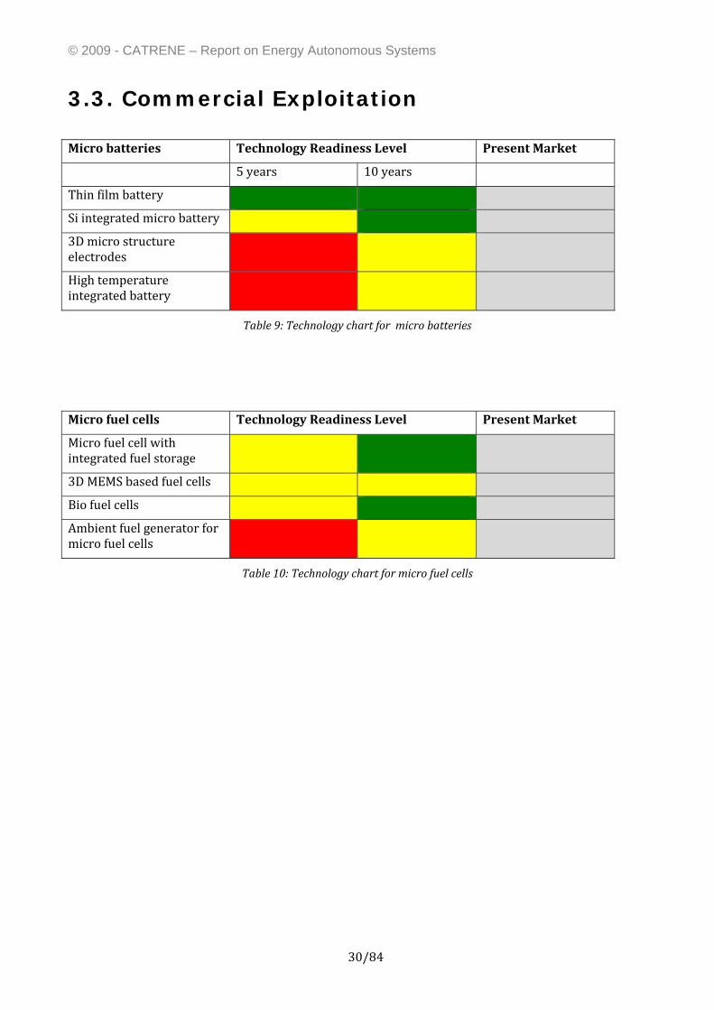
3.3. Commercial Exploitation
Micro batteries Technology Readiness Level Present Market
5 years 10 years
Thin film battery
Si integrated micro battery
3D micro structure electrodes
High temperature integrated battery
Table 9: Technology chart for micro batteries
Micro fuel cells Technology Readiness Level Present Market
Micro fuel cell with integrated fuel storage
3D MEMS based fuel cells
Bio fuel cells
Ambient fuel generator for micro fuel cells
Table 10: Technology chart for micro fuel cells
© 2009 - CATRENE – Report on Energy Autonomous Systems
31/84
4. Current Status of Ultra Low Power (ULP) Systems and Forward Look
4.1. Science and Technology
4.1.1 Radio links
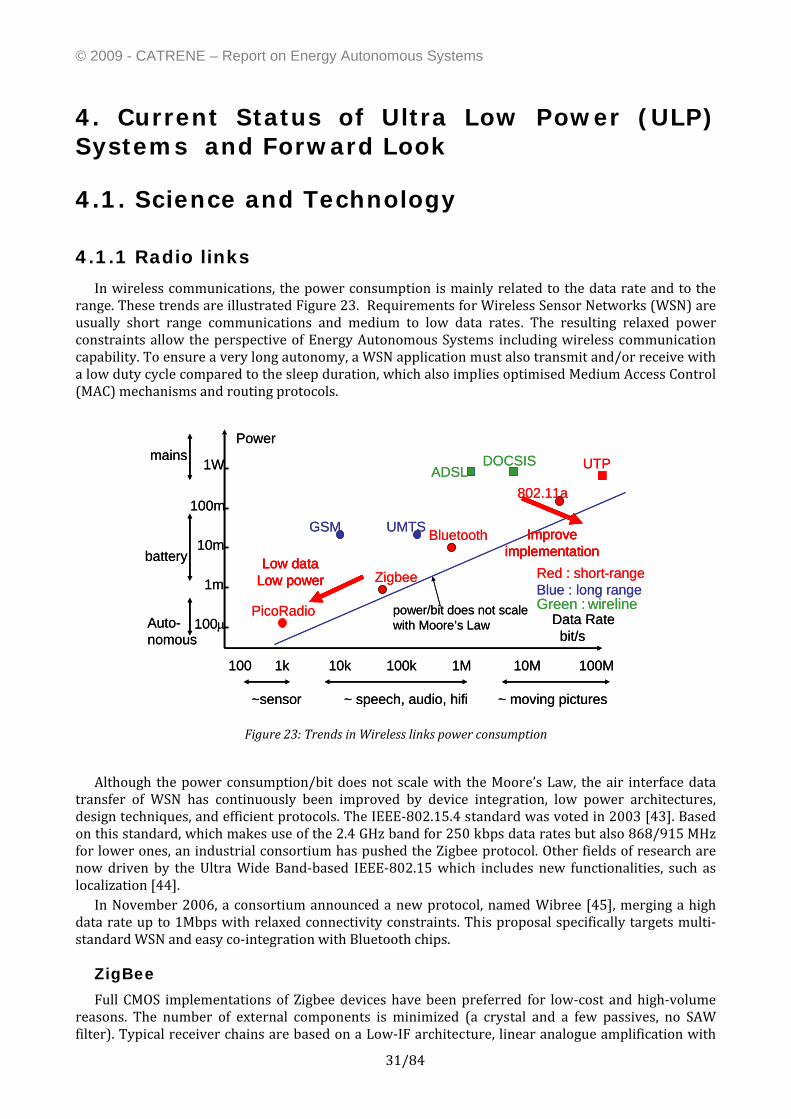
In wireless communications, the power consumption is mainly related to the data rate and to the range. These trends are illustrated Figure 23. Requirements for Wireless Sensor Networks (WSN) are usually short range communications and medium to low data rates. The resulting relaxed power constraints allow the perspective of Energy Autonomous Systems including wireless communication capability. To ensure a very long autonomy, a WSN application must also transmit and/or receive with a low duty cycle compared to the sleep duration, which also implies optimised Medium Access Control (MAC) mechanisms and routing protocols.
Green : wireline
bit/s
Power
10k 100k 1M 10M 100M
1m
10m
100m
1W
BluetoothGSM UMTS
802.11a
Zigbee
~ moving pictures~ speech, audio, hifi~sensor
battery
mains
Data RatePicoRadio
ADSLDOCSIS UTP
Red : short-rangeBlue : long range
power/bit does not scale with Moore’s Law100μAuto-
nomous
1k100
Improveimplementation
Improveimplementation
Low dataLow powerLow data
Low power
Figure 23: Trends in Wireless links power consumption
Although the power consumption/bit does not scale with the Moore’s Law, the air interface data transfer of WSN has continuously been improved by device integration, low power architectures, design techniques, and efficient protocols. The IEEE‐802.15.4 standard was voted in 2003 [43]. Based on this standard, which makes use of the 2.4 GHz band for 250 kbps data rates but also 868/915 MHz for lower ones, an industrial consortium has pushed the Zigbee protocol. Other fields of research are now driven by the Ultra Wide Band‐based IEEE‐802.15 which includes new functionalities, such as localization [44].
In November 2006, a consortium announced a new protocol, named Wibree [45], merging a high data rate up to 1Mbps with relaxed connectivity constraints. This proposal specifically targets multi‐standard WSN and easy co‐integration with Bluetooth chips.
ZigBee
Full CMOS implementations of Zigbee devices have been preferred for low‐cost and high‐volume reasons. The number of external components is minimized (a crystal and a few passives, no SAW filter). Typical receiver chains are based on a Low‐IF architecture, linear analogue amplification with
© 2009 - CATRENE – Report on Energy Autonomous Systems
32/84
AGC and 2 MHz bandwidth filtering. The ADC resolution goes from 1‐bit up to 6‐bits with sampling rates from 4 to 16 MHz. The demodulation and de‐spreading are done after the digital conversion. These low complexity, low power, highly digital architectures are possible thanks to the IEEE‐802.15.4 PHY layer specification, and will benefit from CMOS scaling (0.18 µm or 0.13 µm currently).
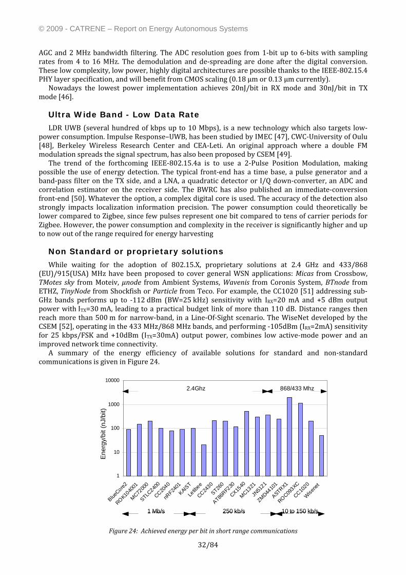
Nowadays the lowest power implementation achieves 20nJ/bit in RX mode and 30nJ/bit in TX mode [46].
Ultra Wide Band - Low Data Rate
LDR UWB (several hundred of kbps up to 10 Mbps), is a new technology which also targets low‐power consumption. Impulse Response–UWB, has been studied by IMEC [47], CWC‐University of Oulu [48], Berkeley Wireless Research Center and CEA‐Leti. An original approach where a double FM modulation spreads the signal spectrum, has also been proposed by CSEM [49].
The trend of the forthcoming IEEE‐802.15.4a is to use a 2‐Pulse Position Modulation, making possible the use of energy detection. The typical front‐end has a time base, a pulse generator and a band‐pass filter on the TX side, and a LNA, a quadratic detector or I/Q down‐converter, an ADC and correlation estimator on the receiver side. The BWRC has also published an immediate‐conversion front‐end [50]. Whatever the option, a complex digital core is used. The accuracy of the detection also strongly impacts localization information precision. The power consumption could theoretically be lower compared to Zigbee, since few pulses represent one bit compared to tens of carrier periods for Zigbee. However, the power consumption and complexity in the receiver is significantly higher and up to now out of the range required for energy harvesting
Non Standard or proprietary solutions
While waiting for the adoption of 802.15.X, proprietary solutions at 2.4 GHz and 433/868 (EU)/915(USA) MHz have been proposed to cover general WSN applications: Micas from Crossbow, TMotes sky from Moteiv, µnode from Ambient Systems, Wavenis from Coronis System, BTnode from ETHZ, TinyNode from Shockfish or Particle from Teco. For example, the CC1020 [51] addressing sub‐GHz bands performs up to ‐112 dBm (BW=25 kHz) sensitivity with IRX=20 mA and +5 dBm output power with ITX=30 mA, leading to a practical budget link of more than 110 dB. Distance ranges then reach more than 500 m for narrow‐band, in a Line‐Of‐Sight scenario. The WiseNet developed by the CSEM [52], operating in the 433 MHz/868 MHz bands, and performing ‐105dBm (IRX=2mA) sensitivity for 25 kbps/FSK and +10dBm (ITX=30mA) output power, combines low active‐mode power and an improved network time connectivity.
A summary of the energy efficiency of available solutions for standard and non‐standard communications is given in Figure 24.
1
10
100
1000
10000
BlueCore2
ROK1040
01
MC7200
0
STLC240
0
CC2040
nRF24
01KAIS
T
Letib
ee
CC2430
ST260
AT86RF2
30
CX1540
MC1321
JN51
21
ZMD4410
1
ASTRX1
ROC093XC
CC1020
Wisene
t
1 Mb/s 250 kb/s 10 to 150 kb/s
2.4Ghz 868/433 Mhz
Ene
rgy/
bit (
nJ/b
it)
1
10
100
1000
10000
BlueCore2
ROK1040
01
MC7200
0
STLC240
0
CC2040
nRF24
01KAIS
T
Letib
ee
CC2430
ST260
AT86RF2
30
CX1540
MC1321
JN51
21
ZMD4410
1
ASTRX1
ROC093XC
CC1020
Wisene
t
1 Mb/s 250 kb/s 10 to 150 kb/s
2.4Ghz 868/433 Mhz
1
10
100
1000
10000
BlueCore2
ROK1040
01
MC7200
0
STLC240
0
CC2040
nRF24
01KAIS
T
Letib
ee
CC2430
ST260
AT86RF2
30
CX1540
MC1321
JN51
21
ZMD4410
1
ASTRX1
ROC093XC
CC1020
Wisene
t
1 Mb/s 250 kb/s 10 to 150 kb/s
2.4Ghz 868/433 Mhz
Ene
rgy/
bit (
nJ/b
it)
Figure 24: Achieved energy per bit in short range communications
© 2009 - CATRENE – Report on Energy Autonomous Systems
33/84
Towards wireless solutions for autonomous systems
Reducing the energy consumption of wireless transmissions is still a key issue for energy autonomous systems. Starting from the 20nJ/bit state of the art, further innovations and refinements at the circuit and architecture levels are required to lower this value towards 5nJ/bit to 1nJ/bit. Exploiting the specificities of those applications is another path towards this reduction. In this perspective, some promising research directions are detailed below.
TRx and Antenna adaptation to the channel
Finely tuning the antenna and the transceiver is a very efficient way to save energy. Co‐designing those two sub‐components considering only the overall impedance matching (no 50Ω, no fixed impedance constraints) is a first direction. To further minimize the energy consumption, the emitter’s power and the receiver’s sensitivity can also be optimised regarding the perturbations caused by the environment on the radio channel. The position or nearby objects can cause mismatches between the antenna and the RF amplifiers, reducing the budget link. In this case, the power of the emitter or the sensitivity of the receiver must be higher to compensate the induced losses of power. This can be compensated by an adaptive method which consists in detecting the antenna’s input impedance and calculate the proper state matching network configuration.
Subsampling architectures
One trend in the transceiver architectures is to move the analog‐to‐digital interface towards higher frequencies, e.g. to IF and even to RF. However, the A/D converters must have enough bandwidth and dynamic range for the entire IF signal including close‐by interferers. Subsampling the IF relaxes the bandwidth constraints of the A/D converter and therefore significantly decreases its power consumption, but requires better anti‐aliasing filtering [53][54]. Introducing high Q components like acoustic wave resonators (ie. BAW for RF frequencies or Lamb Mode resonators for IF frequencies) can contribute to this latter point.
Asymmetric TRX architectures
Wireless sensor systems are quite distinctive from conventional data and voice applications. Sensors have very low data rate, and the data link can be highly asymmetric since most of the data flow from the sensor nodes to the base station. This statement has initiated research activities aiming at asymmetric TRX architectures, as well as specific or dedicated MAC protocols.
As an example, systems have been proposed that utilize impulse UWB as transmitter technology from sensor node to a sink node and a narrow‐band technology in the opposite direction [55]. Narrow‐band signal can also provide wireless power transmission whereas UWB provides higher uplink data‐rate.
In some application scenarios, like the monitoring of artificial and natural structures [57], one can imagine that wireless data flow is exclusively needed in the direction going from the sensor nodes to a residential gateway. The latter can be connected to the mains or to a large portable supply and thus would be subject to very relaxed power constraints. Under this assumption it can be convenient to design simple, very power efficient RF transmitters for the sensor nodes, leaving to the residential gateway a more complex and power hungry receiving task. In an example of this approach a dedicated digital algorithm on the receiver, making use of a pilot tone generated by the transmitter node, can recover an offset of the central transmission frequency of up to 8.2 MHz, with a precision of 7 kHz (8 ppm at 915 MHz). This allows implementing a crystal‐less and very low power (4.4mW @10kb/s and ‐5dbm output power) transmitter architecture [60].
© 2009 - CATRENE – Report on Energy Autonomous Systems
34/84
Wake up radios
As sensor nodes are expected to be active only small portions of time, ultra low power consumption in stand‐by mode, as well as a quick wake up time are both mandatory. Wake up radio architectures have been proposed, most of them based on super‐regeneration (ie. BWRC Picoradio solution). Recent research has shown that MEMS resonators can be used to improve the frequency drift, which is a serious limitation of this architecture. BWRC also introduced this year a new concept named Uncertain‐IF Architecture [61] which achieves 50μW of RX power consumption at 0.5V supply, using a crystal‐less architecture and periodic calibration.
Asymmetric architectures also try to optimise the transmitter wake up time to save energy.
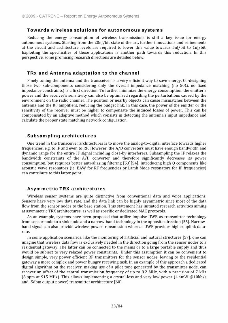
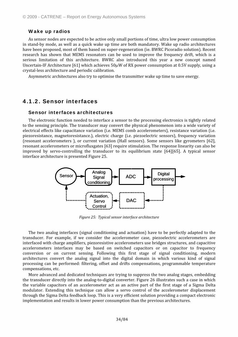
4.1.2. Sensor interfaces
Sensor interfaces architectures
The electronic function needed to interface a sensor to the processing electronics is tightly related to the sensing principle. The transducer may convert the physical phenomenon into a wide variety of electrical effects like capacitance variation (i.e. MEMS comb accelerometers), resistance variation (i.e. piezoresistance, magnetoresistance.), electric charge (i.e. piezoelectric sensors), frequency variation (resonant accelerometers ), or current variation (Hall sensors). Some sensors like gyrometers [62], resonant accelerometers or microfluxgates [63] require stimulation. The response linearity can also be improved by servo‐controlling the transducer to its equilibrium state [64][65]. A typical sensor interface architecture is presented Figure 25.
SensorAnalogSignal
conditioningADC Digital
processing
Actuation,Servo
ControlDAC
SensorAnalogSignal
conditioningADC Digital
processing
Actuation,Servo
ControlDAC
Figure 25: Typical sensor interface architecture
The two analog interfaces (signal conditioning and actuation) have to be perfectly adapted to the transducer. For example, if we consider the accelerometer case, piezoelectric accelerometers are interfaced with charge amplifiers, piezoresistive accelerometers use bridges structures, and capacitive accelerometers interfaces may be based on switched capacitors or on capacitor to frequency conversion or on current sensing. Following this first stage of signal conditioning, modern architectures convert the analog signal into the digital domain in which various kind of signal processing can be performed: filtering, offset and drifts compensations, programmable temperature compensations, etc.
More advanced and dedicated techniques are trying to suppress the two analog stages, embedding the transducer directly into the analog‐to‐digital converter. Figure 26 illustrates such a case in which the variable capacitors of an accelerometer act as an active part of the first stage of a Sigma Delta modulator. Extending this technique can allow a servo control of the accelerometer displacement through the Sigma Delta feedback loop. This is a very efficient solution providing a compact electronic implementation and results in lower power consumption than the previous architectures.

© 2009 - CATRENE – Report on Energy Autonomous Systems
35/84
ADC∫+-
Acceleration Vout
DAC
XV
XVElectrostatic force
Non-electrical domain electrical domain
ADC∫+-
Acceleration Vout
DAC
XV
XVElectrostatic force
Non-electrical domain electrical domain
Figure 26: Example of a sensor embedded into a ΣΔ architecture
As already mentioned, some transducers like gyrometers may require very sophisticated architectures [62], embedding several levels of servo‐control. Designing such architectures and circuits requires setting up a heterogeneous design flow, allowing to model and co‐simulate the transducer with electronics.
ADCs are consequently a key element of sensor interfaces architectures. Typical requirements in autonomous sensor networks applications are a low bandwidth (100Hz to some tens of kHz), a medium to high resolution (10 to 14bits, required for further digital compensations like drift, offset, etc.) and power dissipation as low as possible.
Sensor interfaces have to address two different tradeoffs: power/resolution and dedicated/versatile sensor interface.
Ultra low power ADC
Several families of ADC architectures exist [66][68]: flash, half‐flash, dual‐slope, folding, successive approximation register (SAR), pipelined, sigma‐delta, etc. In order to compare these different ADCs figures‐of‐merit are proposed, some of them taking into account the power consumption [68]54]. Thanks to progress in technology, architectures and design, there has been overtime a continuous improvement of these figures. Today, thanks to this evolution [73], most state of the art ADC developments reach a FOM value lower than a few of pico‐Joules per sampling (pJ/s) .
Due to the specific requirements of sensors interfaces (low Power, low Bandwidth, Medium to High resolution), SAR or Sigma Delta ADCs are frequently used. The advantages of SAR ADCs are their range of speeds, resolutions as well as low cost and low power dissipation. Power optimized SAR ADC developed in state of the art CMOS technology can reach a Figure of Merit of less than 0.1pJ/sample [72] and absolute power consumption of less than 4μW for typical wireless sensor performance (100kb/s, 9.4 Effective Number of Bits (ENOB) [75]).
When 14 to 16 bits resolution is required, sigma‐delta ADCs are the only alternative. The prize to pay is the need of a high over‐sampling rate. As a result, high‐resolution sigma‐delta ADC consume more power. A comparison of recently published (ISSCC,JSSC) Sigma‐delta ADCs can be found in [69] and [71].
Capacitive sensor interfaces (most of them embedding an ADC) have followed the same trend, with figures of merit continuously improving over time. Note that in Figure 27, some industrial products may embed extra functionalities when compared to research work, leading to additional power consumption.
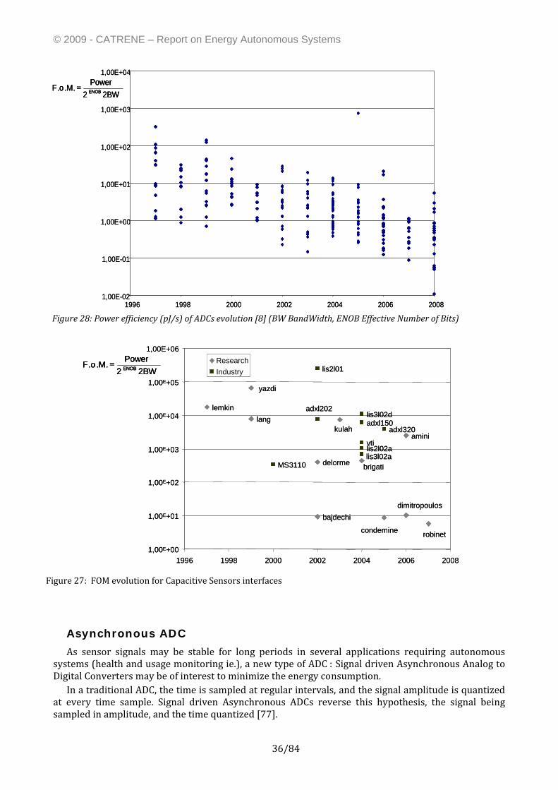
© 2009 - CATRENE – Report on Energy Autonomous Systems
36/84
Asynchronous ADC
As sensor signals may be stable for long periods in several applications requiring autonomous systems (health and usage monitoring ie.), a new type of ADC : Signal driven Asynchronous Analog to Digital Converters may be of interest to minimize the energy consumption.
In a traditional ADC, the time is sampled at regular intervals, and the signal amplitude is quantized at every time sample. Signal driven Asynchronous ADCs reverse this hypothesis, the signal being sampled in amplitude, and the time quantized [77].
Figure 28: Power efficiency (pJ/s) of ADCs evolution [8] (BW BandWidth, ENOB Effective Number of Bits)
BW22Power
.M.o.F ENOB=
1,00E-02
1,00E-01
1,00E+00
1,00E+01
1,00E+02
1,00E+03
1,00E+04
1996 1998 2000 2002 2004 2006 2008
BW22Power
.M.o.F ENOB=
BW22Power
.M.o.F ENOB=
1,00E-02
1,00E-01
1,00E+00
1,00E+01
1,00E+02
1,00E+03
1,00E+04
1996 1998 2000 2002 2004 2006 2008
robinet
dimitropoulos
amini
condemine
brigati
kulah
delorme
bajdechi
lang
yazdi
lemkin
adxl320
vti
lis3l02d
lis3l02alis2l02a
adxl150
lis2l01
adxl202
MS3110
1,00E+00
1,00E+01
1,00E+02
1,00E+03
1,00E+04
1,00E+05
1,00E+06
1996 1998 2000 2002 2004 2006 2008
ResearchIndustryBW22
Power.M.o.F ENOB=
robinet
dimitropoulos
amini
condemine
brigati
kulah
delorme
bajdechi
lang
yazdi
lemkin
adxl320
vti
lis3l02d
lis3l02alis2l02a
adxl150
lis2l01
adxl202
MS3110
1,00E+00
1,00E+01
1,00E+02
1,00E+03
1,00E+04
1,00E+05
1,00E+06
1996 1998 2000 2002 2004 2006 2008
ResearchIndustryBW22
Power.M.o.F ENOB=
BW22Power
.M.o.F ENOB=
Figure 27: FOM evolution for Capacitive Sensors interfaces
© 2009 - CATRENE – Report on Energy Autonomous Systems
37/84
Several recent research works have been dealing with this family of converters [78], [79], [80]. In [79] for instance, a tracking converter is adapted to an amplitude sampling. This type of architecture allows an asynchronous conversion, whose power consumption is linearly correlated to the input signal activity. [80] demonstrates significant gains in activity and power compared to a Nyquist sampling converter.
The major drawback of those amplitude sampling converters is the incompatibility of the output data with the usual signal processing algorithms. Recent research works are targeting signal processing for asynchronous data [81][82].
Time domain converters
In order to expand the input voltage range and to improve signal‐to‐noise ratio (SNR) at extremely low power supply voltages, recent works have proposed a new family of ADC in the time domain. Those converters are composed of the cascade of an analog‐to‐time converter and a time‐to‐digital converter. ADCs working down to 500mV and even 200mV have been demonstrated [83][84]. One example of this trend is to tune the frequency of a voltage‐controlled oscillator (VCO) according to the input analog voltage, and then measure the period of the oscillator to determine the quantized output value Traditional conversion structures , like Single slope, Delta, Sigma Delta, flash, are used, transposed in the time domain.
Wake-up sensors
As well as being able to wake‐up on a radio signal, it may be interesting for several energy autonomous applications to wake‐up on external physical phenomena reaching a threshold. One approach is to have a continuous measurement and to check those input data. A first level of energy optimization can be obtained by relaxing the measurement specifications in this mode. Other approaches have proposed to use dedicated MEMS [85]: the threshold(s) is(are) directly embedded into the transducer structure. This leads to extremely low energy consumption in wake‐up mode. Between those two approaches, an important research topic is probably to define sensor architectures (transducer+ electronic) whose both components are adaptable to the two operating modes: wake‐up and measurement.
4.1.3. Digital Processing
Ultra low power DSP
INTRODUCTION DSP algorithms and DSP systems are more and more used in high volume applications, such as
portable phones, hard‐disk drives, audio and image processing, hearing aids, wired and wireless communication devices. DSP algorithms can be implemented in hardware random logic or on programmable DSP cores. Random logic will provide the largest performances in silicon area, speed and power consumption. However, unlike programmable DSP processors, random logic is not flexible at all. A given DSP algorithms is implemented in silicon and cannot be modified. It is why more and more programmable DSP are used in various applications to be capable of using the provided flexibility to modify/improve/correct the embedded software. Regarding performances, in [86][87][88], there are some estimations of the energy for different DSP architectures.
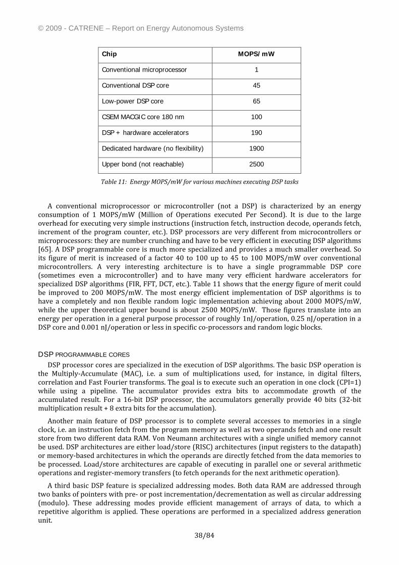
© 2009 - CATRENE – Report on Energy Autonomous Systems
38/84
Chip MOPS/mW
Conventional microprocessor 1
Conventional DSP core 45
Low-power DSP core 65
CSEM MACGIC core 180 nm 100
DSP + hardware accelerators 190
Dedicated hardware (no flexibility) 1900
Upper bond (not reachable) 2500
Table 11: Energy MOPS/mW for various machines executing DSP tasks
A conventional microprocessor or microcontroller (not a DSP) is characterized by an energy consumption of 1 MOPS/mW (Million of Operations executed Per Second). It is due to the large overhead for executing very simple instructions (instruction fetch, instruction decode, operands fetch, increment of the program counter, etc.). DSP processors are very different from microcontrollers or microprocessors: they are number crunching and have to be very efficient in executing DSP algorithms [65]. A DSP programmable core is much more specialized and provides a much smaller overhead. So its figure of merit is increased of a factor 40 to 100 up to 45 to 100 MOPS/mW over conventional microcontrollers. A very interesting architecture is to have a single programmable DSP core (sometimes even a microcontroller) and to have many very efficient hardware accelerators for specialized DSP algorithms (FIR, FFT, DCT, etc.). Table 11 shows that the energy figure of merit could be improved to 200 MOPS/mW. The most energy efficient implementation of DSP algorithms is to have a completely and non flexible random logic implementation achieving about 2000 MOPS/mW, while the upper theoretical upper bound is about 2500 MOPS/mW. Those figures translate into an energy per operation in a general purpose processor of roughly 1nJ/operation, 0.25 nJ/operation in a DSP core and 0.001 nJ/operation or less in specific co‐processors and random logic blocks.
DSP PROGRAMMABLE CORES DSP processor cores are specialized in the execution of DSP algorithms. The basic DSP operation is
the Multiply‐Accumulate (MAC), i.e. a sum of multiplications used, for instance, in digital filters, correlation and Fast Fourier transforms. The goal is to execute such an operation in one clock (CPI=1) while using a pipeline. The accumulator provides extra bits to accommodate growth of the accumulated result. For a 16‐bit DSP processor, the accumulators generally provide 40 bits (32‐bit multiplication result + 8 extra bits for the accumulation).
Another main feature of DSP processor is to complete several accesses to memories in a single clock, i.e. an instruction fetch from the program memory as well as two operands fetch and one result store from two different data RAM. Von Neumann architectures with a single unified memory cannot be used. DSP architectures are either load/store (RISC) architectures (input registers to the datapath) or memory‐based architectures in which the operands are directly fetched from the data memories to be processed. Load/store architectures are capable of executing in parallel one or several arithmetic operations and register‐memory transfers (to fetch operands for the next arithmetic operation).
A third basic DSP feature is specialized addressing modes. Both data RAM are addressed through two banks of pointers with pre‐ or post incrementation/decrementation as well as circular addressing (modulo). These addressing modes provide efficient management of arrays of data, to which a repetitive algorithm is applied. These operations are performed in a specialized address generation unit.
© 2009 - CATRENE – Report on Energy Autonomous Systems
39/84
The fourth basic feature is the capability to perform efficiently loops with zero overhead. Loop or repeat instructions are able to repeat 1 to N instructions without loop counter (no need to initialize and to up‐date a loop counter). These instructions are fetched from the memory and stored in a small cache memory in which they are read during the execution of the loop.
LOW-POWER DSP CORES First DSP cores were processors, for instance, the DSP Group (now CEVA) Pine DSP processors,
integrated in 0.8 or 0.6 micron technologies in 1992. A single MAC per clock was executed and the energy efficiency was about 0.5 MOPS/mW. In 1996, the Motorola 56800 [90][91] was also executing one MAC per clock providing 0.4 MOPS/mW. The computation power of such DSP cores was about 20 to 50 MOPS (so Millions of Operations executed Per Second) at 20 to 50 MHz. It is interesting to note [92] that an energy‐efficient architecture is the one in which the main sources of power dissipation are operators. In a general‐purpose processor, there is a waste of power due to load/store, branch, prediction, etc.
However, in the mid nineties, many applications (audio, video, baseband) were requiring much more computation power, at least of a factor 10 up to 500 MOPS, but sometimes of a factor 100 (5000 MOPS). Much more parallel DSP cores were mandatory. Different architectures were proposed:
VLIW machines Customizable DSP cores Re‐configurable machines DSP with hardware accelerators Multicore DSP processors
For autonomous platforms consuming under 100 μW, only some specialized architectures can be used. For instance, VLIW cores such as TMS320C6x [89][90][91], reconfigurable FPGA‐based [93] or reconfigurable computer architecture like DART [92], cannot be used for such ultra low power SoCs. Even multicore DSP is not always a good approach for reducing power. For achieving an ultra low power consumption or energy, one is forced to reduce significantly the throughput (or computation power) of the processor as well as to use a very low supply voltage. For dynamic power, it is good to try to increase significantly the parallelism to be capable of executing many operations per clock and therefore the throughput. However, this approach is not very good today regarding leakage power in deep submicron technologies that is roughly proportional to the number of logic gates and therefore increases too much with the parallelism.
For customizable and reconfigurable DSP cores, the key point is to reconfigure only a limited number of units within the DSP core, such as some execution units and addressing units [94]. The latter are interesting, as the operands fetch from memory is generally a severe bottleneck in parallel machines for which 8‐16 operands are required each clock cycle. So, sophisticated addressing modes can be dynamically reconfigured depending on the DSP task to be executed. The DSP MACGIC designed at CSEM [94][95] shows an example in which several addressing modes can be reconfigured depending on the user’s algorithms. In Table 2, four DSP cores are compared. Starcore is a VLIW core (128‐bit instruction). MACGIC has 4 MAC in parallel and has a limited reconfiguration mechanism for addressing modes. Icyflex is a combination RISC 32‐bit with a DSP based on 2 MAC in parallel. CoolFlux is a very small DSP with 2 MAC but with only 2 memory transfers per clock. It is clear that for achieving a power consumption of 100 μW, the maximum frequency allowed is less than 1 MHz. However, Table 2 shows that these DSP cores are capable of executing a maximum of up to 32 operations per clock (Starcore and MACGIC), 16 for icyflex and only 8 for CoolFlux. So the throughput even at 0.5 MHz is still 0.5 *32 = 16 MOPS. The last rows of Table 12 show a comparison in energy, taking into account the power/MHz and the number of clocks that is required for a given DSP algorithms (complex 256 point FFT).
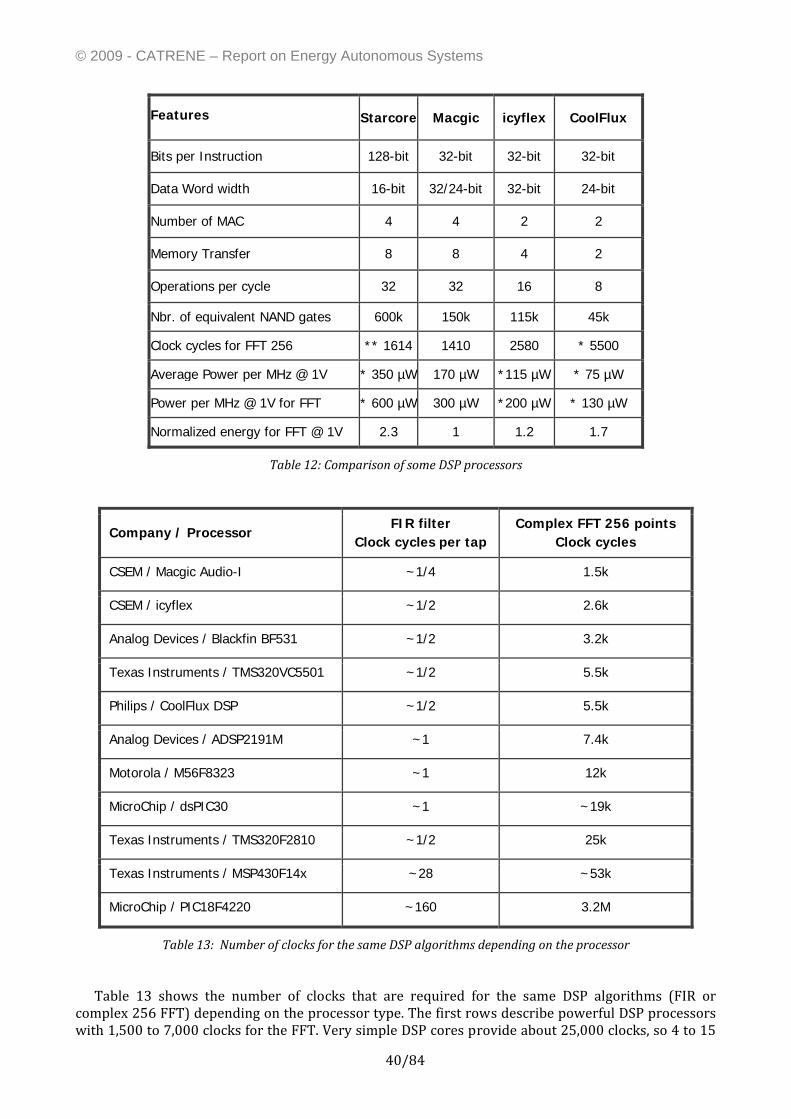
© 2009 - CATRENE – Report on Energy Autonomous Systems
40/84
Features Starcore Macgic icyflex CoolFlux
Bits per Instruction 128-bit 32-bit 32-bit 32-bit
Data Word width 16-bit 32/24-bit 32-bit 24-bit
Number of MAC 4 4 2 2
Memory Transfer 8 8 4 2
Operations per cycle 32 32 16 8
Nbr. of equivalent NAND gates 600k 150k 115k 45k
Clock cycles for FFT 256 ** 1614 1410 2580 * 5500
Average Power per MHz @ 1V * 350 µW 170 µW *115 µW * 75 µW
Power per MHz @ 1V for FFT * 600 µW 300 µW *200 µW * 130 µW
Normalized energy for FFT @ 1V 2.3 1 1.2 1.7
Table 12: Comparison of some DSP processors
Company / Processor FIR filter
Clock cycles per tap Complex FFT 256 points
Clock cycles
CSEM / Macgic Audio-I ~1/4 1.5k
CSEM / icyflex ~1/2 2.6k
Analog Devices / Blackfin BF531 ~1/2 3.2k
Texas Instruments / TMS320VC5501 ~1/2 5.5k
Philips / CoolFlux DSP ~1/2 5.5k
Analog Devices / ADSP2191M ~1 7.4k
Motorola / M56F8323 ~1 12k
MicroChip / dsPIC30 ~1 ~19k
Texas Instruments / TMS320F2810 ~1/2 25k
Texas Instruments / MSP430F14x ~28 ~53k
MicroChip / PIC18F4220 ~160 3.2M
Table 13: Number of clocks for the same DSP algorithms depending on the processor
Table 13 shows the number of clocks that are required for the same DSP algorithms (FIR or complex 256 FFT) depending on the processor type. The first rows describe powerful DSP processors with 1,500 to 7,000 clocks for the FFT. Very simple DSP cores provide about 25,000 clocks, so 4 to 15
© 2009 - CATRENE – Report on Energy Autonomous Systems
41/84
times more. It is also interesting to note that the famous MSP 430 requires 53,000 clocks and a very small PIC 3 millions clocks. One can see here the benefits of more and more specialized processor architectures.
To have more performance in DSP processors, a quite obvious rule can be applied: to design more specialized architectures, datapaths and addressing units, well adapted to the algorithms that have to be executed. This trend could go to design random logic machines, such as the hearing aid presented in [96], for which a very specialized architecture has been designed. However, flexibility and programmability are lost, and most customers require being capable of programming their DSP processor.
The architecture based on co‐processors or hardware accelerators is definitively the best one regarding power consumption. Each DSP task uses the minimal number of transistors and transitions to perform its work. The control code unavoidable in every application is also efficiently executed on the microcontroller or on the simple DSP, and some unexpected DSP tasks can be executed on the simple DSP if no accelerator is available. It is certainly very efficient in terms of energy. However, the main issue is the software mapping of a given application onto so many heterogeneous processors and co‐processors. Transistor count could be high and some co‐processors fully useless for some applications. Regarding leakage, unused engines have to be cut off from the supply voltages, resulting in complex procedures to start/stop them.
There is a clear trend for multicore architecture for high performance microprocessors. It is however not so clear if arrays of identical DSP cores is a valid trend for DSPs. During the last years, a lot of research has been performed on arrays of identical parallel DSP processors, but no commercial chip resulted. It is an open question to know if this trend for embedded processors will also occur for DSPs. Some recently announced chips do have hundreds of identical DSP cores, such as the PicoChip 102 with 344 processors, most of them capable of executing MAC operations. It is a massive parallelism running at relatively low frequencies (160 MHz) but delivering a huge power computation [97]. But such architectures could also be operated at less than 1 MHz frequency and very low voltage for providing a spectacular decrease in energy consumption.
One can be easily convinced that the choice of a DSP architecture for ultra low power platforms is very depending on the application [98]. An analysis of the application has to be performed to check what are the heavy workloads as well as a dynamic execution profile [99], in such a way to choose if co‐processors are useful, how many, etc. In addition, some of these categories can be combined, as shown in [98], where a DSP architecture is constructed with a microcontroller and reconfigurable co‐processors and reconfigurable communication network.
Standby mode & leakage reduction
There are a lot of leakage current scenarios, depending on the circuit state. The circuit can be in ACTIVE mode or in SLEEP mode. The leakage reduction techniques are at the DESIGN stage. RUNTIME based solutions can be added for further improvement. It is generally much more difficult to reduce leakage in active modes. In the following, we will address this problem at three design levels: CIRCUIT Level, GATE Level and ARCHITECTURE Level.
LEAKAGE REDUCTION AT CIRCUIT LEVEL The leakage reduction techniques are also quite complex as several different sources of leakage do
exist, and some techniques could be used for reduction of subthreshold leakage at the cost of increasing the gate leakage!
Basically, subthreshold leakage reduction is performed by: Using several VT Modifying statically or dynamically the VT (forward and backward biasing techniques). Vdd cut‐off by sleep transistors MTCMOS
© 2009 - CATRENE – Report on Energy Autonomous Systems
42/84
DTCMOS Swapped Bodies Triple S Subthreshold Logic
Some other techniques can be added, such as channel doping, halo doping, multiple channel lengths and some techniques specialized to cache memories, but they will not be covered by the following. So refer to [100].
Gate leakage is another story. The gate‐tunnelling leakage can be reduced by using high threshold, thick‐oxide sleep transistors. Another method for reducing the gate‐tunnelling leakage is using dual oxide technology. This method is analogous to the dual threshold technique for reducing the sub‐threshold leakage. This method can be combined with the dual threshold technique to reduce both sub‐threshold and gate‐tunnelling leakage.
LEAKGE REDUCTION AT LOGIC GATE LEVEL At the gate level, several techniques have been used:
Transistor stacking technique Minimum Leakage Input Vector Transistor & Pin Reordering for Gate Leakage Reduction
LEAKAGE REDUCTION AT ARCHITECTURE LEVEL Starting from 0.18 μm technologies, static power consumption, due to leaky “off” transistors, is now
a non negligible source of power dissipation even in running mode. Thus, the total power consumption (i.e. dynamic plus static power) has to be optimized instead of simply reducing dynamic power, which is due to switched capacitance charge/discharge.
Many research efforts aim at reducing the static power consumption at the device level using for instance MTCMOS, VTCMOS, Gated‐Vdd, or DTCMOS (see previous documents). Conversely very few papers considered the joint static‐dynamic power optimization at a higher level, namely at system and architectural levels.
For a given architecture, reducing the supply voltage Vdd leads to a reduction of dynamic power consumption, whereas it also results in a decrease of performance or speed. To compensate this effect, the threshold voltage Vth should be reduced too. Unfortunately, lowering the Vth exponentially increases the static power consumption. At a certain point, this increase in static power consumption becomes larger than the gain in dynamic power and the total power consumption becomes larger.
Therefore, between all the combinations of Vdd/Vth guaranteeing the desired speed, only one couple will result in the lowest power consumption [102]. From now on, these working conditions will be called optimal working point or ideal working point. The location of this optimal working point and its associated total power consumption are tightly related to architectural and technology parameters.
Reducing the activity allows reducing Ptot, whereas it tends to increase the optimal Vdd and Vth. As architectural modifications will change simultaneously several factors (not just the activity), it is necessary to develop a methodology to evaluate the influence of such transformations on Ptot. The originality of this approach is that at this optimal point, there is a given ratio between dynamic and static power, strongly correlated to the ratio between Ion/Ioff of the technology. This ratio is smaller and smaller due to leaky transistors. On the other hand, the ratio between dynamic and static power is dependent on architectural parameters, which are the activity a and the logical depth LD (number of gates in series). The formula is:
aLDk
II
off
on ⋅= 1
© 2009 - CATRENE – Report on Energy Autonomous Systems
43/84
If the Ion/Ioff ratio is small (100 to 500), one can see that LD has to be small and activity quite large! It is why we could see some paradigm shift, as activity has until now been a main factor to be reduced. It was due to the fact that only the dynamic power was considered. With static and dynamic power, the activity has not to be as small as possible, as very inactive gates or transistors doing nearly nothing are leaky devices. So it is not optimal to have too many gates or transistors doing nothing as they are leaky devices! The parameter k1 is the ratio between dynamic and static power; it is roughly between 1 and 5.
There are different methodologies to find the best architectures (activity, logical depth) regarding total power consumption at this optimal point (Vdd. Vth).
1) Vdd and Vth can be freely (and precisely) modified. Whereas the supply voltage is in general easily controllable, it is harder to modify the threshold voltage as body back‐biasing becomes less and less efficient in smaller technologies. Reference [100] (NewCAS’04) explores new design methodologies for designing leakage tolerant digital architectures, based on architectural parameters like activity, logical depth, number of transitions for achieving a given task and total number of gates. Various architectures for a same logic function are compared at very low Vdd and VT that define the optimal total power consumption of each architecture. Reference [101] (PATMOS’04) focuses on architecture comparison and aims at selecting the one with the minimum total power consumption by simultaneously optimizing static and dynamic power dissipation. This optimal power has been estimated for eleven 16‐bit multiplier architectures. On the other hand it is possible to select a technology that matches as closely as possible the Vdd and Vth requirements.
2) A methodology for which Vdd and Vth are fixed, given as constraints provided by the applications. So the methodology allows to compare several architectures (or micro‐architectures) performing the same function and to select the one presenting the smallest total power consumption under fixed supply voltage (Vdd), threshold voltage (Vth) and frequency (f) constraints. The smallest total power consumption, which is closely related to the architecture, results clearly from a trade‐off between static and dynamic power. Static power reduction leads to select architectures with a small number of cells and not with a small number of transitions, as it was the case when only dynamic power reduction was targeted. Reference [103] (JOLPE’05) demonstrates this methodology, which is applied to the selection of the lowest power consuming architecture among a set of eleven 16 bit multipliers.
Finally, an approximated closed‐form total power consumption equation for circuits working at their optimal supply and threshold voltage can be found [104]. Comparisons of this formula to the numerical calculation show an error less than 3% on a set of thirteen 16 bit multipliers. Starting from this equation, the influence of architecture transformations (including pipelining, parallelization, sequentialization) on the optimal total power can be discussed. Finally, by a similar approach, the impact of the technology choice on achievable power saving can be considered, showing how a moderated trade‐off between leakage and speed is the key characteristic of a good low power technology.
Subthreshold logic
In digital circuits, power is needed to charge the load capacitance C of each logic node at the switching frequency f. This dynamic power consumption can be expressed as dddyn VVCfP ⋅Δ⋅⋅= where Vdd is the supply voltage and ΔV the logic voltage swing, smaller or equal to Vdd. Thus the dynamic power can be reduced by reducing ΔV. But this gate voltage swing is needed to ensure a sufficient current ratio Ion/Ioff in the transistors producing the transitions. Indeed, the on‐current Ion must be large enough to ensure transitions at the required speed, and Ioff should be as small as possible to limit the static power consumption Pstat = Ioff ⋅ Vdd between transitions.
© 2009 - CATRENE – Report on Energy Autonomous Systems
44/84
The swing ΔV needed to achieve a given value of Ion/Ioff can be reduced by reducing the gate voltage overhead, until it becomes minimum when weak inversion is reached. Logic circuits based on transistors operated in weak inversion (also called subthreshold) therefore offer minimum possible operating voltage, and thereby minimum Pdyn for a given Pstat. However, this is only possible if the threshold voltage of the transistors can be precisely adapted to this very low value of supply voltage Vdd. The feasibility of CMOS inverters with supply voltages as low as 200 mV was already demonstrated more than 30 years ago [107]. However, the minimum channel length was still of the order of 5 μm, limiting the maximum frequency to just a few hundred kHz, therefore the idea was buried for several decades dominated by the struggle for maximum speed. It has been revived recently [108] and applied to complete subsystems operated below 200 mV [109][110]. In the meantime, weak inversion was used extensively for very low‐power analog circuits [111][112], and a special model was developed to better describe the behavior MOS transistor from weak to strong inversion [113][114]. Reference [106] relies on this experience of weak inversion and on this model to derive the analytical results needed to optimize such low‐voltage digital circuits and to identify their ultimate limits.
There are two approaches to design subthreshold circuits: Minimal energy or Minimal power. Minimal energy considers that Threshold Voltages (VT) are fixed. So Vdd is reduced to under VT, resulting in lower frequencies and larger clock period. So dynamic power is reduced, static power is decreased, but the static energy is increased as more time is required to execute the logic function. So there is an optimum in energy. This optimal energy is also depending on logic depth and activity factor [116]. The minimal Vdd (and minimal energy) is smaller for small logical depth and for large activity factors. Reference [115] shows this optimum for Vdd=0.4 Volt with VT at 0.4 Volt. Analysis in [117] and chip measurements in [118] showed that minimum energy per operation occurs in sub‐VT region. An 8‐TT sub‐VT SRAM in 65nm CMOS was demonstrated [119], and more complex sub‐VT processors are appearing [120].
Minimal power subthreshold circuits have been described above in the section “Leakage reduction at architecture level” in section “Standby mode & leakage reduction”.
Asynchronous logic
Asynchronous microprocessors provide some advantages over synchronous architectures, such as no clock tree, no skew, no clock power, no PLL, easy restart after an idle state, and some disadvantages, such as a more difficult design and a lack of CAD tools.
Asynchronous design can be performed as:
− dual rail logic, in which data are encoded as "01" and "10" for respectively "0" and "1". If a precharged logic is used, both true and complemented outputs are precharged to "1", and it is possible to detect the end of the computation when both the outputs are "01" or "10". Such a scheme is insensitive to delays but requires twice the logic of a conventional implementation.
− bundled‐data, in which conventional logic is used with an additional control wire which indicates when the output is valid. The end of an operation is provided by a delay, which is the worst delay of the operator. It means that the operator doesn’t work in mean delay, but in worst delay (some important advantages of asynchronous logic is lost). This style was also used for the AMULET.
The AMULET1 microprocessor [121][122][123] was an asynchronous implementation of the ARM6 32‐bit RISC microprocessor. It is based on the micropipelines of Sutherland which use a bundled data implementation using a transition protocol. The design of the AMULET1 is based on several cooperating micropipelines. The main memory, also pipelined, sends instructions to the pipelined instruction decoder. Instructions are prefetched as far ahead as the capacities of the various elastic pipeline buffers allow. After a branch, some instructions in the micropipeline are invalid and must be discarded. Memory data accesses are interleaved with instruction fetches though the memory pipeline.
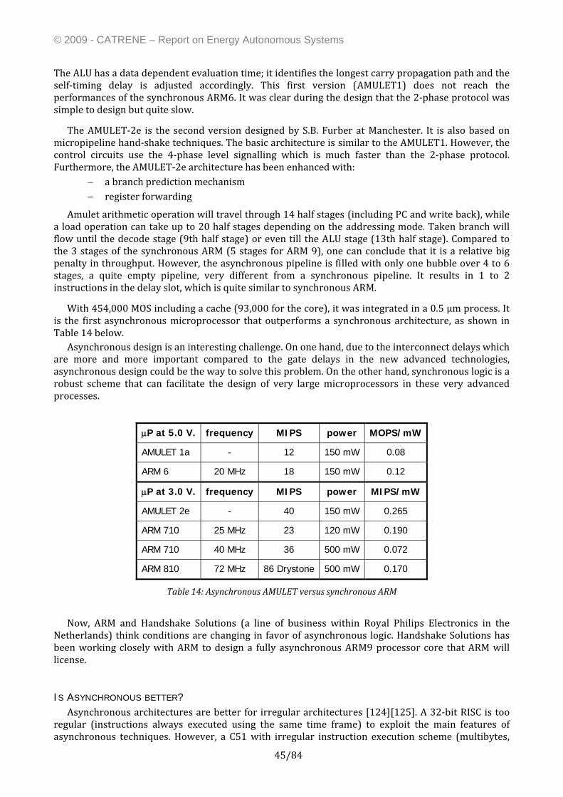
© 2009 - CATRENE – Report on Energy Autonomous Systems
45/84
The ALU has a data dependent evaluation time; it identifies the longest carry propagation path and the self‐timing delay is adjusted accordingly. This first version (AMULET1) does not reach the performances of the synchronous ARM6. It was clear during the design that the 2‐phase protocol was simple to design but quite slow.
The AMULET‐2e is the second version designed by S.B. Furber at Manchester. It is also based on micropipeline hand‐shake techniques. The basic architecture is similar to the AMULET1. However, the control circuits use the 4‐phase level signalling which is much faster than the 2‐phase protocol. Furthermore, the AMULET‐2e architecture has been enhanced with:
− a branch prediction mechanism − register forwarding
Amulet arithmetic operation will travel through 14 half stages (including PC and write back), while a load operation can take up to 20 half stages depending on the addressing mode. Taken branch will flow until the decode stage (9th half stage) or even till the ALU stage (13th half stage). Compared to the 3 stages of the synchronous ARM (5 stages for ARM 9), one can conclude that it is a relative big penalty in throughput. However, the asynchronous pipeline is filled with only one bubble over 4 to 6 stages, a quite empty pipeline, very different from a synchronous pipeline. It results in 1 to 2 instructions in the delay slot, which is quite similar to synchronous ARM.
With 454,000 MOS including a cache (93,000 for the core), it was integrated in a 0.5 µm process. It is the first asynchronous microprocessor that outperforms a synchronous architecture, as shown in Table 14 below.
Asynchronous design is an interesting challenge. On one hand, due to the interconnect delays which are more and more important compared to the gate delays in the new advanced technologies, asynchronous design could be the way to solve this problem. On the other hand, synchronous logic is a robust scheme that can facilitate the design of very large microprocessors in these very advanced processes.
μP at 5.0 V. frequency MIPS power MOPS/mW
AMULET 1a - 12 150 mW 0.08
ARM 6 20 MHz 18 150 mW 0.12
μP at 3.0 V. frequency MIPS power MIPS/mW
AMULET 2e - 40 150 mW 0.265
ARM 710 25 MHz 23 120 mW 0.190
ARM 710 40 MHz 36 500 mW 0.072
ARM 810 72 MHz 86 Drystone 500 mW 0.170
Table 14: Asynchronous AMULET versus synchronous ARM
Now, ARM and Handshake Solutions (a line of business within Royal Philips Electronics in the
Netherlands) think conditions are changing in favor of asynchronous logic. Handshake Solutions has been working closely with ARM to design a fully asynchronous ARM9 processor core that ARM will license.
IS ASYNCHRONOUS BETTER? Asynchronous architectures are better for irregular architectures [124][125]. A 32‐bit RISC is too
regular (instructions always executed using the same time frame) to exploit the main features of asynchronous techniques. However, a C51 with irregular instruction execution scheme (multibytes,
© 2009 - CATRENE – Report on Energy Autonomous Systems
46/84
multicycles) is better for asynchronous architectures [126], as asynchronous handshaking allows the machine to wait naturally that long operations are finished to start the next operations. It seems also that asynchronous logic is better for digital filters working for hearing aids [127]. The 16‐bit Aspro microprocessor from TIMA, Grenoble, is a very fast and very low power asynchronous microprocessor [128].
The Value proposition of asynchronous is better and better due to the following:
− Clock trees are more and more difficult to design − GALS (Globally Asynchronous Locally Synchronous) [132][133]: is it a paradigm shift? − Low power can be achieved with new design methodologies [129][134] − For smartcards, security is one of the major issue, and synchronous architectures are more
sensitive to DPA (Diffential Power Attack). It has been shown that asynchronous architectures can be more resistant to DPA [130].
− In deep sleep mode, PLL and oscillators are stopped, and it takes perhaps one second to restart. It is not the case for asynchronous, that provides an easy and natural restart after deep sleep mode.
Fault tolerant architectures & logic
ERROR DETECTION SEQUENTIAL CIRCUITS Error‐detection sequential circuits have been proposed to monitor on‐line timing faults of digital
circuits within the presence of environmental influences and reliability concerns. The combination of timing‐error detection and error‐recovery circuits [135][136][137] enables the digital function to operate at either a maximal frequency for a nominal power supply, or a minimal power supply for a given frequency. When dynamic variations induce a timing error, the error is detected and corrected to maintain proper functionality. This allows to eliminate guardbands that are usually taken to compensate for variabilities (Voltage, Temperature, Process). Further benefits are possible by exploiting critical path‐activation probabilities [137]. If the slowest paths on the die are infrequently activated, the power supply voltage may decrease lower than the critical path operating voltage. When these critical paths are activated, the timing error is detected and corrected. Total power reduction between 30% to 40% has been reported [138].
PROBABILISTIC CMOS The foundations of PCMOS technology are rooted in physics of computation, algorithms, and
information theory using techniques derived from physics of computation and information theory. Probalistic CMOS was introduced in 2003 by Krishna V. Palem. Palem [139][140] showed that the thermodynamic cost of computing a bit of information irreversibly is directly related to its probability p of being correct. The minimum energy for a bit computation kT⋅ln(2) becomes kT⋅ln(2p) for the probabilistic CMOS.
Further, using an abstract model of computation, it has been demonstrated that switch level energy savingscan be harnessed at the application level to construct probabilistic algorithms. In previous work, the application of PCMOS at the device level (switch behavior) [140] and at the architecture level (probabilistic applications and PSoC) [141] was demonstrated to be feasible. The specific algorithms that were studied in the first works included Bayesian networks, random neural networks, and hyper‐encryption. These algorithms span embedded application domains such as face and pattern recognition, spoken alphabet recognition, and computer security. This principal of probabilistic computing can be further expanded into error‐tolerant applications in the form of building blocks
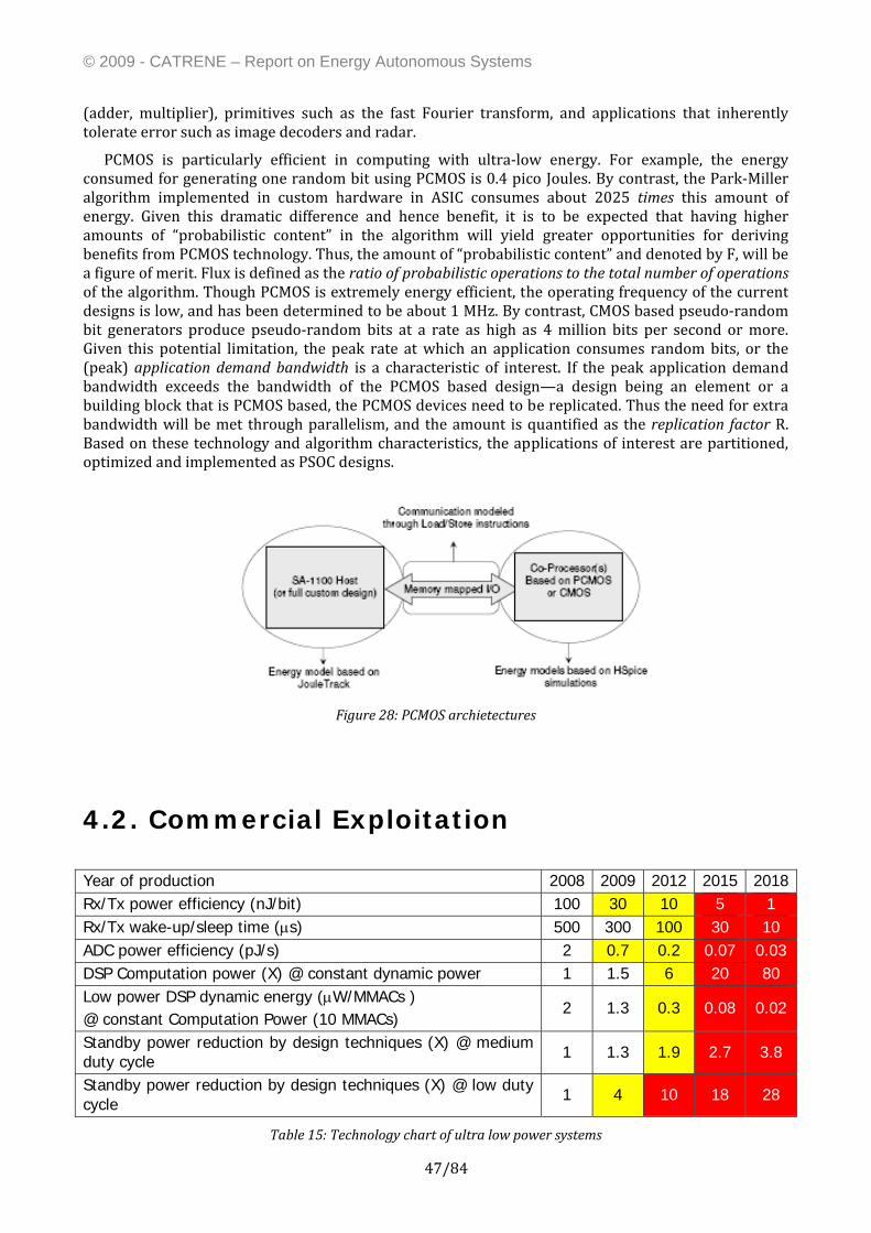
© 2009 - CATRENE – Report on Energy Autonomous Systems
47/84
(adder, multiplier), primitives such as the fast Fourier transform, and applications that inherently tolerate error such as image decoders and radar.
PCMOS is particularly efficient in computing with ultra‐low energy. For example, the energy consumed for generating one random bit using PCMOS is 0.4 pico Joules. By contrast, the Park‐Miller algorithm implemented in custom hardware in ASIC consumes about 2025 times this amount of energy. Given this dramatic difference and hence benefit, it is to be expected that having higher amounts of “probabilistic content” in the algorithm will yield greater opportunities for deriving benefits from PCMOS technology. Thus, the amount of “probabilistic content” and denoted by F, will be a figure of merit. Flux is defined as the ratio of probabilistic operations to the total number of operations of the algorithm. Though PCMOS is extremely energy efficient, the operating frequency of the current designs is low, and has been determined to be about 1 MHz. By contrast, CMOS based pseudo‐random bit generators produce pseudo‐random bits at a rate as high as 4 million bits per second or more. Given this potential limitation, the peak rate at which an application consumes random bits, or the (peak) application demand bandwidth is a characteristic of interest. If the peak application demand bandwidth exceeds the bandwidth of the PCMOS based design—a design being an element or a building block that is PCMOS based, the PCMOS devices need to be replicated. Thus the need for extra bandwidth will be met through parallelism, and the amount is quantified as the replication factor R. Based on these technology and algorithm characteristics, the applications of interest are partitioned, optimized and implemented as PSOC designs.
Figure 28: PCMOS archietectures
4.2. Commercial Exploitation
Year of production 2008 2009 2012 2015 2018Rx/Tx power efficiency (nJ/bit) 100 30 10 5 1 Rx/Tx wake-up/sleep time (μs) 500 300 100 30 10 ADC power efficiency (pJ/s) 2 0.7 0.2 0.07 0.03 DSP Computation power (X) @ constant dynamic power 1 1.5 6 20 80 Low power DSP dynamic energy (μW/MMACs ) @ constant Computation Power (10 MMACs)
2 1.3 0.3 0.08 0.02
Standby power reduction by design techniques (X) @ medium duty cycle 1 1.3 1.9 2.7 3.8
Standby power reduction by design techniques (X) @ low duty cycle 1 4 10 18 28
Table 15: Technology chart of ultra low power systems

© 2009 - CATRENE – Report on Energy Autonomous Systems
48/84
Wireless transmission power efficiency will likely be improved in a first step by increasing the data rate at a fixed power.
Minimizing the wake‐up time and associated energy consumption will require a shift from Quartz based time reference to other time reference like NEMS based ones.
Considering the average specifications of sensor nodes ADCs (low bandwidth, medium resolution), ADCs power efficiency will continue to benefit from the parasitics reduction brought by the technology scaling, but new conversion architectures will be necessary at a stage to fully exploit this. Higher resolutions are more impacted by thermal noise and might not follow the same trend.
In Table 15 two figures about the computation power are given. The first one considers the applications that will require an increase in computing performances, while the second one considers applications that will be mostly driven by the size and the autonomy.
The standby power reduction figures assume that the ITRS leakage targets for LSTP technologies will be met. However, when moving to very advanced nodes, random technological variabilities will seriously impact the overall circuit leakage and will require new design techniques to cope with.
© 2009 - CATRENE – Report on Energy Autonomous Systems
49/84
5. Current status of Power Management (PM) and Forward Look
5.1. Science and Technology
The output of an energy harvester is not directly suited as power supply for circuits because of variations in its power and voltage. A power management system is then required. It is an advanced conversion circuit, for very low feeding power, that adapts its input to the energy harvester and its output to the load.
The development of a power management circuit faces the following challenges:
As seen in Chapter 2, vibration or thermal energy and visible or RF electromagnetic radiation can be used as ambient energy source. A wide variety of harvesters then exists, they have different electrical characteristics and require specific interfacing (e.g. their output can be AC or DC, high voltage/low current or low voltage/high current.)
The AC or DC amplitudes are changing depending on the environmental conditions.
The availability of the energy source is varying over time.
Depending on the voltage level of the primary energy, system start‐up may become nontrivial.
The ease of designing a power management system depends on the available level of power and on the available space. Large power, large size systems are easy to handle, to the contrary small power, small size systems call for the use of miniaturized, highly efficient circuits.
Harvesters can be categorized in two groups. Thermoelectric generators and solar cells generate a variable DC‐output voltage. A DC‐DC‐converter with a variable conversion factor and a controller are required here to provide the battery with the correct signal. Vibration and RF energy harvesters, on the other hand, produce an AC‐output voltage. For this type of harvesters, an extra AC‐DC‐converter stage is required.
Each energy harvester has an operation point where the extracted electrical energy is maximized. This maximum power point depends on the individual properties of the energy harvester. Maximum power is achieved by adapting the input impedance to the maximum power point of the harvester. A controller is required to do this.
When the harvester generates less energy than the energy used by the controller and the converters, the power management system has to shut down and ensure that it does not discharge the output. When there’s again enough power available, the power management system has to start up again.
A battery management circuit can be required to ensure safe operating conditions when a battery is charged at the output.
5.1.1. Photovoltaic and Thermal Before discussing the state‐of‐the‐art in power management circuits for energy harvesters, we
briefly introduce the generalities of DC‐DC converters and maximum power point tracking algorithms that can be used in combination with photovoltaic and thermal harvesters.
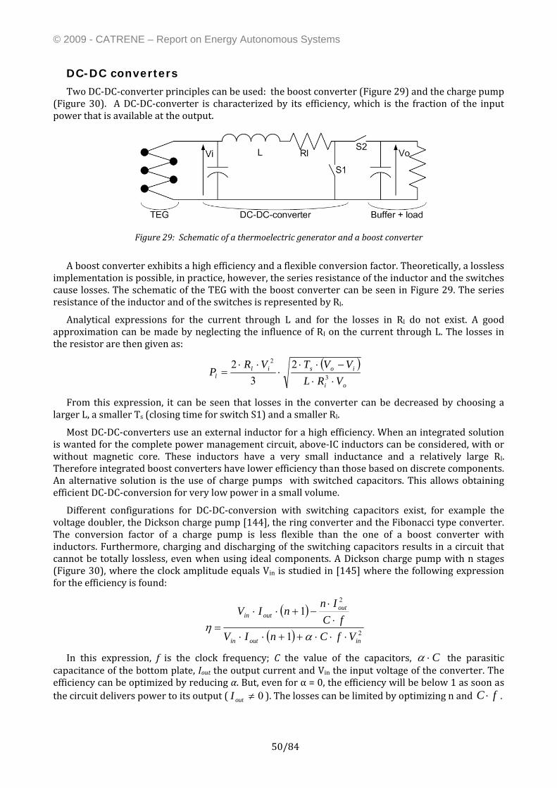
© 2009 - CATRENE – Report on Energy Autonomous Systems
50/84
DC-DC converters
Two DC‐DC‐converter principles can be used: the boost converter (Figure 29) and the charge pump (Figure 30). A DC‐DC‐converter is characterized by its efficiency, which is the fraction of the input power that is available at the output.
Figure 29: Schematic of a thermoelectric generator and a boost converter
A boost converter exhibits a high efficiency and a flexible conversion factor. Theoretically, a lossless implementation is possible, in practice, however, the series resistance of the inductor and the switches cause losses. The schematic of the TEG with the boost converter can be seen in Figure 29. The series resistance of the inductor and of the switches is represented by Rl.
Analytical expressions for the current through L and for the losses in Rl do not exist. A good approximation can be made by neglecting the influence of Rl on the current through L. The losses in the resistor are then given as:
( )oi
iosill VRL
VVTVRP
⋅⋅−⋅⋅
⋅⋅⋅
= 3
2 23
2
From this expression, it can be seen that losses in the converter can be decreased by choosing a larger L, a smaller Ts (closing time for switch S1) and a smaller Rl.
Most DC‐DC‐converters use an external inductor for a high efficiency. When an integrated solution is wanted for the complete power management circuit, above‐IC inductors can be considered, with or without magnetic core. These inductors have a very small inductance and a relatively large Rl. Therefore integrated boost converters have lower efficiency than those based on discrete components. An alternative solution is the use of charge pumps with switched capacitors. This allows obtaining efficient DC‐DC‐conversion for very low power in a small volume.
Different configurations for DC‐DC‐conversion with switching capacitors exist, for example the voltage doubler, the Dickson charge pump [144], the ring converter and the Fibonacci type converter. The conversion factor of a charge pump is less flexible than the one of a boost converter with inductors. Furthermore, charging and discharging of the switching capacitors results in a circuit that cannot be totally lossless, even when using ideal components. A Dickson charge pump with n stages (Figure 30), where the clock amplitude equals Vin is studied in [145] where the following expression for the efficiency is found:
( )
( ) 2
2
1
1
inoutin
outoutin
VfCnIVfC
InnIV
⋅⋅⋅++⋅⋅⋅⋅
−+⋅⋅=
αη
In this expression, f is the clock frequency; C the value of the capacitors, C⋅α the parasitic capacitance of the bottom plate, Iout the output current and Vin the input voltage of the converter. The efficiency can be optimized by reducing α. But, even for α = 0, the efficiency will be below 1 as soon as the circuit delivers power to its output ( 0≠outI ). The losses can be limited by optimizing n and fC ⋅ .
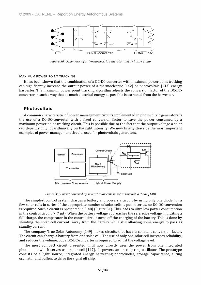
© 2009 - CATRENE – Report on Energy Autonomous Systems
51/84
Figure 30: Schematic of a thermoelectric generator and a charge pump
MAXIMUM POWER POINT TRACKING It has been shown that the combination of a DC‐DC‐converter with maximum power point tracking
can significantly increase the output power of a thermoelectric [142] or photovoltaic [143] energy harvester. The maximum power point tracking algorithm adjusts the conversion factor of the DC‐DC‐converter in such a way that as much electrical energy as possible is extracted from the harvester.
Photovoltaic
A common characteristic of power management circuits implemented in photovoltaic generators is the use of a DC‐DC‐converter with a fixed conversion factor to save the power consumed by a maximum power point tracking circuit. This is possible due to the fact that the output voltage a solar cell depends only logarithmically on the light intensity. We now briefly describe the most important examples of power management circuits used for photovoltaic generators.
Figure 31: Circuit powered by several solar cells in series through a diode [148]
The simplest control system charges a battery and powers a circuit by using only one diode, for a few solar cells in series. If the appropriate number of solar cells is put in series, no DC‐DC‐conversion is required. Such a circuit is presented in [148] (Figure 31). This leads to ultra low power consumption in the control circuit (< 7 µA). When the battery voltage approaches the reference voltage, indicating a full charge, the comparator in the control circuit turns off the charging of the battery. This is done by shunting the solar cell current away from the battery while still allowing some energy to pass as standby current.
The company True Solar Autonomy [149] makes circuits that have a constant conversion factor. The circuit can charge a battery from one solar cell. The use of only one solar cell increases reliability, and reduces the volume, but a DC‐DC‐converter is required to adjust the voltage level.
The most compact circuit presented until now directly uses the power from one integrated photodiode, which serves as a solar cell [147]. It powers an on‐chip ring oscillator. The prototype consists of a light source, integrated energy harvesting photodiodes, storage capacitance, a ring oscillator and buffers to drive the signal off chip.
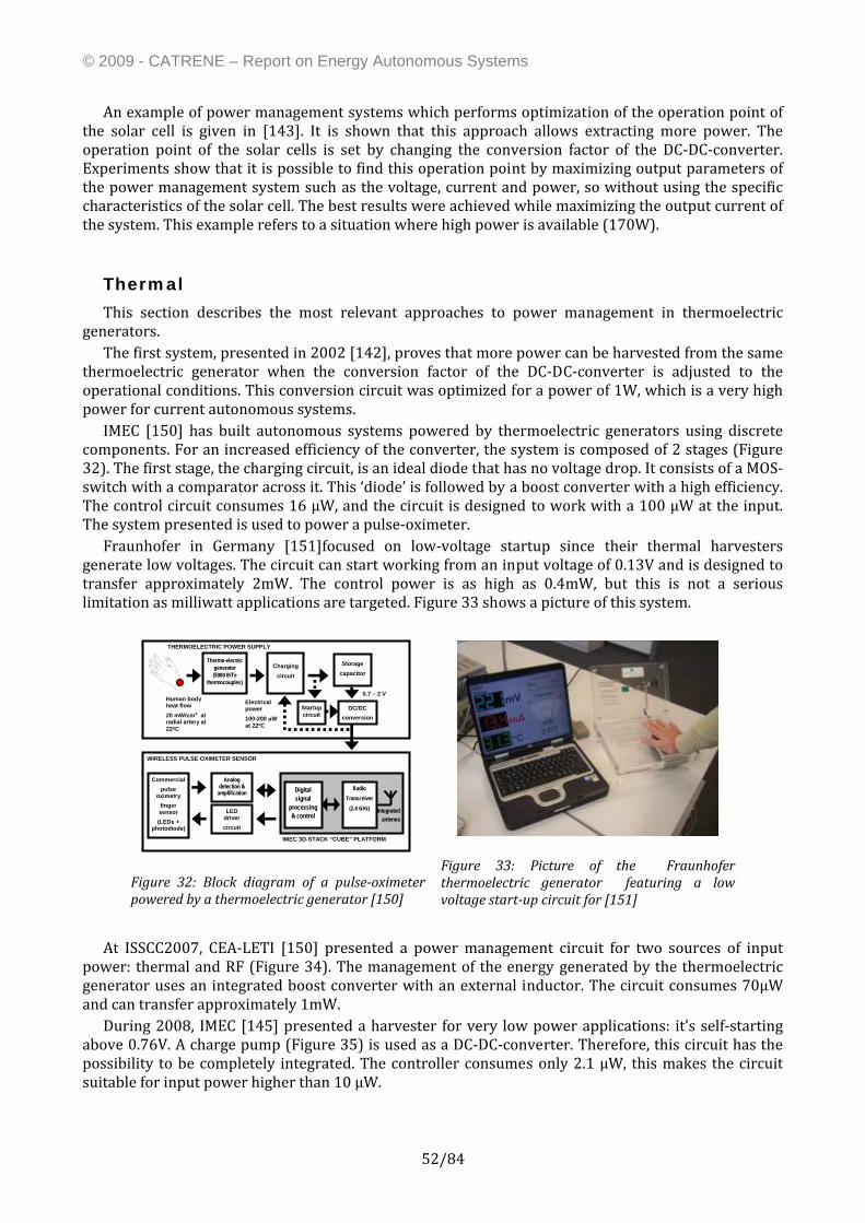
© 2009 - CATRENE – Report on Energy Autonomous Systems
52/84
An example of power management systems which performs optimization of the operation point of the solar cell is given in [143]. It is shown that this approach allows extracting more power. The operation point of the solar cells is set by changing the conversion factor of the DC‐DC‐converter. Experiments show that it is possible to find this operation point by maximizing output parameters of the power management system such as the voltage, current and power, so without using the specific characteristics of the solar cell. The best results were achieved while maximizing the output current of the system. This example refers to a situation where high power is available (170W).
Thermal
This section describes the most relevant approaches to power management in thermoelectric generators.
The first system, presented in 2002 [142], proves that more power can be harvested from the same thermoelectric generator when the conversion factor of the DC‐DC‐converter is adjusted to the operational conditions. This conversion circuit was optimized for a power of 1W, which is a very high power for current autonomous systems.
IMEC [150] has built autonomous systems powered by thermoelectric generators using discrete components. For an increased efficiency of the converter, the system is composed of 2 stages (Figure 32). The first stage, the charging circuit, is an ideal diode that has no voltage drop. It consists of a MOS‐switch with a comparator across it. This ‘diode’ is followed by a boost converter with a high efficiency. The control circuit consumes 16 µW, and the circuit is designed to work with a 100 µW at the input. The system presented is used to power a pulse‐oximeter.
Fraunhofer in Germany [151]focused on low‐voltage startup since their thermal harvesters generate low voltages. The circuit can start working from an input voltage of 0.13V and is designed to transfer approximately 2mW. The control power is as high as 0.4mW, but this is not a serious limitation as milliwatt applications are targeted. Figure 33 shows a picture of this system.
Figure 32: Block diagram of a pulseoximeter powered by a thermoelectric generator [150]
Figure 33: Picture of the Fraunhofer thermoelectric generator featuring a low voltage startup circuit for [151]
At ISSCC2007, CEA‐LETI [150] presented a power management circuit for two sources of input
power: thermal and RF (Figure 34). The management of the energy generated by the thermoelectric generator uses an integrated boost converter with an external inductor. The circuit consumes 70µW and can transfer approximately 1mW.
During 2008, IMEC [145] presented a harvester for very low power applications: it’s self‐starting above 0.76V. A charge pump (Figure 35) is used as a DC‐DC‐converter. Therefore, this circuit has the possibility to be completely integrated. The controller consumes only 2.1 µW, this makes the circuit suitable for input power higher than 10 µW.
WIRELESS PULSE OXIMETER SENSOR
Commercial pulse
oximetry finger sensor (LEDs +
photodiode)
Analog detection &
amplification
LED driver circuit
Digital signal
processing& control
Radio Transceiver
(2.4 GHz) Integratedantenna
IMEC 3D-STACK “CUBE” PLATFORM
Human body heat flow 20 mW/cm² at radial artery at 22ºC
Thermo-electric generator (5000 BiTe
thermocouples)
Charging circuit
Electrical power 100-200 µW at 22ºC
Storage capacitor
0.7 – 2 V
DC/DCconversion
THERMOELECTRIC POWER SUPPLY
Startup circuit
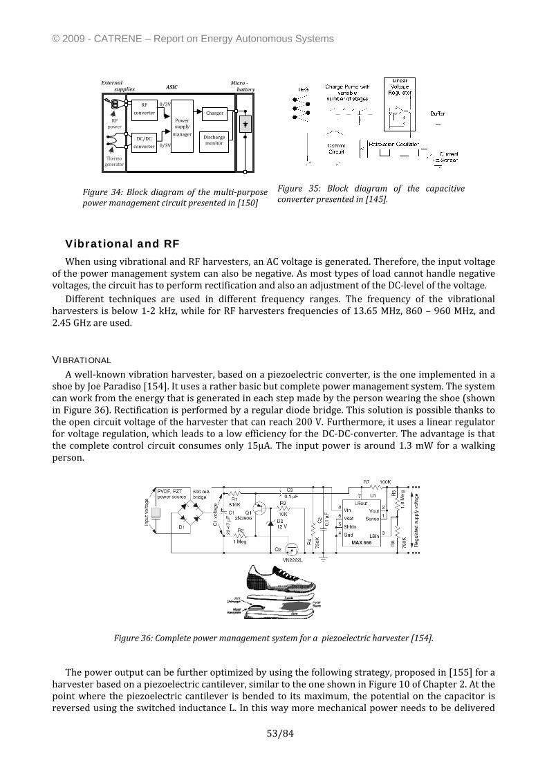
© 2009 - CATRENE – Report on Energy Autonomous Systems
53/84
Figure 34: Block diagram of the multipurpose power management circuit presented in [150]
Figure 35: Block diagram of the capacitive converter presented in [145].
Vibrational and RF
When using vibrational and RF harvesters, an AC voltage is generated. Therefore, the input voltage of the power management system can also be negative. As most types of load cannot handle negative voltages, the circuit has to perform rectification and also an adjustment of the DC‐level of the voltage.
Different techniques are used in different frequency ranges. The frequency of the vibrational harvesters is below 1‐2 kHz, while for RF harvesters frequencies of 13.65 MHz, 860 – 960 MHz, and 2.45 GHz are used.
VIBRATIONAL A well‐known vibration harvester, based on a piezoelectric converter, is the one implemented in a
shoe by Joe Paradiso [154]. It uses a rather basic but complete power management system. The system can work from the energy that is generated in each step made by the person wearing the shoe (shown in Figure 36). Rectification is performed by a regular diode bridge. This solution is possible thanks to the open circuit voltage of the harvester that can reach 200 V. Furthermore, it uses a linear regulator for voltage regulation, which leads to a low efficiency for the DC‐DC‐converter. The advantage is that the complete control circuit consumes only 15µA. The input power is around 1.3 mW for a walking person.
Figure 36: Complete power management system for a piezoelectric harvester [154].
The power output can be further optimized by using the following strategy, proposed in [155] for a harvester based on a piezoelectric cantilever, similar to the one shown in Figure 10 of Chapter 2. At the point where the piezoelectric cantilever is bended to its maximum, the potential on the capacitor is reversed using the switched inductance L. In this way more mechanical power needs to be delivered
0/3V
0/3V
Power supply manager
Charger
Micro battery
External supplies ASIC
Thermo generator
RF power
DC/DC converter
Discharge monitor
RF converter
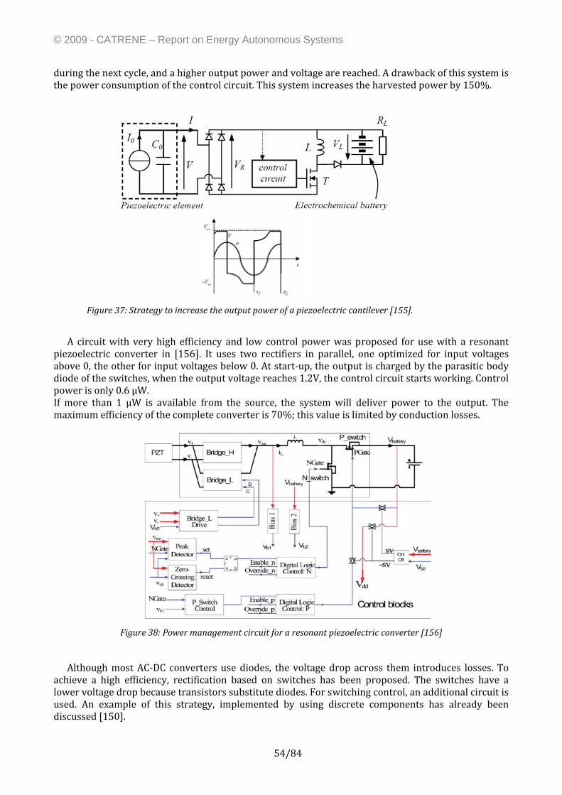
© 2009 - CATRENE – Report on Energy Autonomous Systems
54/84
during the next cycle, and a higher output power and voltage are reached. A drawback of this system is the power consumption of the control circuit. This system increases the harvested power by 150%.
Figure 37: Strategy to increase the output power of a piezoelectric cantilever [155].
A circuit with very high efficiency and low control power was proposed for use with a resonant
piezoelectric converter in [156]. It uses two rectifiers in parallel, one optimized for input voltages above 0, the other for input voltages below 0. At start‐up, the output is charged by the parasitic body diode of the switches, when the output voltage reaches 1.2V, the control circuit starts working. Control power is only 0.6 µW. If more than 1 µW is available from the source, the system will deliver power to the output. The maximum efficiency of the complete converter is 70%; this value is limited by conduction losses.
Figure 38: Power management circuit for a resonant piezoelectric converter [156]
Although most AC‐DC converters use diodes, the voltage drop across them introduces losses. To achieve a high efficiency, rectification based on switches has been proposed. The switches have a lower voltage drop because transistors substitute diodes. For switching control, an additional circuit is used. An example of this strategy, implemented by using discrete components has already been discussed [150].
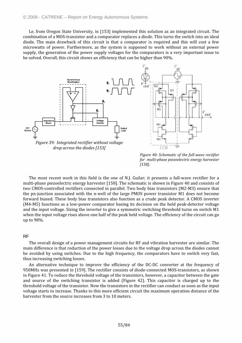
© 2009 - CATRENE – Report on Energy Autonomous Systems
55/84
Le, from Oregon State University, in [153] implemented this solution as an integrated circuit. The combination of a MOS‐transistor and a comparator replaces a diode. This turns the switch into an ideal diode. The main drawback of this circuit is that a comparator is required and this will cost a few microwatts of power. Furthermore, as the system is supposed to work without an external power supply, the generation of the power supply voltages for the comparators is a very important issue to be solved. Overall, this circuit shows an efficiency that can be higher than 90%.
Figure 39: Integrated rectifier without voltage
drop across the diodes [153]
Figure 40: Schematic of the fullwave rectifier for multiphase piezoelectric energy harvester [158].
The most recent work in this field is the one of N.J. Guilar; it presents a full‐wave rectifier for a
multi‐phase piezoelectric energy harvester [158]. The schematic is shown in Figure 40 and consists of two CMOS‐controlled rectifiers connected in parallel. Two body bias transistors (M2‐M3) ensure that the pn‐junction associated with the n‐well of the large PMOS power transistor M1 does not become forward biased. These body bias transistors also function as a crude peak detector. A CMOS inverter (M4‐M5) functions as a low‐power comparator basing its decision on the held peak‐detector voltage and the input voltage. Sizing the inverter to give a symmetric switching threshold turns on switch M1 when the input voltage rises above one half of the peak held voltage. The efficiency of the circuit can go up to 98%.
RF The overall design of a power management circuits for RF and vibration harvester are similar. The
main difference is that reduction of the power losses due to the voltage drop across the diodes cannot be avoided by using switches. Due to the high frequency, the comparators have to switch very fast, thus increasing switching losses.
An alternative technique to improve the efficiency of the DC‐DC converter at the frequency of 950MHz was presented in [159]. The rectifier consists of diode‐connected MOS‐transistors, as shown in Figure 41. To reduce the threshold voltage of the transistors, however, a capacitor between the gate and source of the switching transistor is added (Figure 42). This capacitor is charged up to the threshold voltage of the transistor. Now the transistors in the rectifier can conduct as soon as the input voltage starts to increase. Thanks to this more efficient circuit the maximum operation distance of the harvester from the source increases from 3 to 10 meters.

© 2009 - CATRENE – Report on Energy Autonomous Systems
56/84
Figure 41: NMOStype rectifier with diodeconnected transistors [157]
Figure 42: Proposed NMOStype rectifier in [157]
5.3. Commercial Exploitation
We can distinguish two types of power management systems. Systems build with off‐the‐shelf components and integrated systems based on ASIC.
The former have been demonstrated and tested and are ready for commercialization. There is still margin for improvement by using better performing components (e.g..: passives with less parasitic, IC’s with improved functionality).
Integrated systems for power management circuits for energy harvesters are under development, and some are already used in a relevant environment. There is still room for major improvements by using existing CMOS‐technologies. But also in this case, the development of new CMOS technologies and improved passive components can lead to more efficient and more flexible circuits.
Solar cells and some macroscopic vibration/thermal harvesters are at a level of technological development which allows integration with a power management circuit and commercialization of the complete systems. These devices occupy a large volume and generate a relatively large power, making the design of the power management system easier.
Microscopic devices are still at a prototype level; this obviously hinders the commercialization of related power management systems. The status and evolution of technology is given in Table 16.
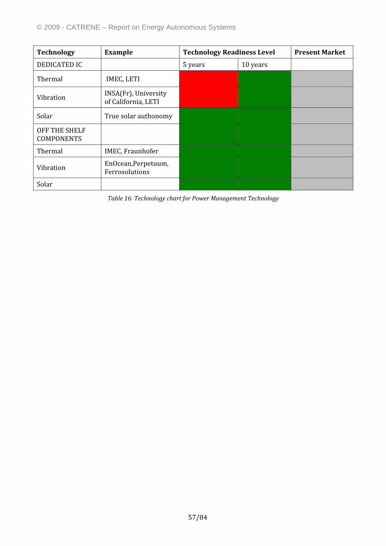
© 2009 - CATRENE – Report on Energy Autonomous Systems
57/84
Technology Example Technology Readiness Level Present Market
DEDICATED IC 5 years 10 years
Thermal IMEC, LETI
Vibration INSA(Fr), Universityof California, LETI
Solar True solar authonomy
OFF THE SHELF COMPONENTS
Thermal IMEC, Fraunhofer
Vibration EnOcean,Perpetuum, Ferrosolutions
Solar
Table 16: Technology chart for Power Management Technology
© 2009 - CATRENE – Report on Energy Autonomous Systems
58/84
6. European Situation and Forward Look
6.1. Overview of Funding and Supporting Actions
In Europe large research institutions tackle the various aspects of autonomous sensors and actuators networks. At CEA/LETI, MINATEC, Fraunhofer, IMEC the research on power‐management is closely coordinated with the one on harvesters and low power radio. These institutions are already capable of fabricating simple but complete sensor nodes. The coordination of the various activities increases the impact of their work and makes it more effective.
A limited number of Universities, small research groups and companies are also active in the field of power management research. Their work is in general of high quality, contributes to create a community with a reasonably large critical mass and to orient young people at the end of their university formation towards this field.
The importance of energy harvesting has motivated the German federal government to include the topic in its €500 million research support program that started in 2007. However, funding is mainly public and definitely not abundant. At European level no Integrated Projects has been founded and only one Strategic Targeted Research Project, addressing harvesting and power management (VIBES, http://www.vibes.ecs.soton.ac.uk), has been financed in the FP6. The topic is also covered in some Integrated Projects dedicated to sensor networks (e.g. Sensation, http://www.sensation‐eu.org and e‐CUBE, http://ecubes.epfl.ch).
Evolution of macroscopic vibration and thermal harvesters and of solar cells will be market driven,
technology is ready and both cost reduction and performance improvements are possible. Microscopic vibration harvesters are still far from a product, their evolution will be technology
driven. In order to accelerate technology development it is very important to coordinate the activities of small research groups, SME and Universities which address only a specific aspect of the wireless sensor networks. International projects are the key tool to bring together the groups active on harvesters, low power transceivers, data processing, and power management.
Design of integrated systems and principle of power electronics are basis courses of any engineering curriculum and they are enough to prepare people with specific competences in the design of power electronics for harvesters. Effectiveness of the system designer will be increased by a better knowledge of state of the art technology.
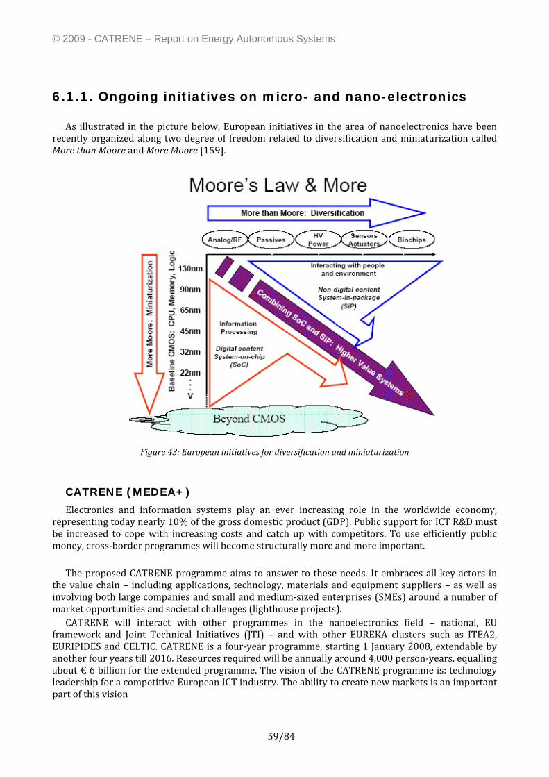
© 2009 - CATRENE – Report on Energy Autonomous Systems
59/84
6.1.1. Ongoing initiatives on micro- and nano-electronics As illustrated in the picture below, European initiatives in the area of nanoelectronics have been
recently organized along two degree of freedom related to diversification and miniaturization called More than Moore and More Moore [159].
Figure 43: European initiatives for diversification and miniaturization
CATRENE (MEDEA+)
Electronics and information systems play an ever increasing role in the worldwide economy, representing today nearly 10% of the gross domestic product (GDP). Public support for ICT R&D must be increased to cope with increasing costs and catch up with competitors. To use efficiently public money, cross‐border programmes will become structurally more and more important.
The proposed CATRENE programme aims to answer to these needs. It embraces all key actors in
the value chain – including applications, technology, materials and equipment suppliers – as well as involving both large companies and small and medium‐sized enterprises (SMEs) around a number of market opportunities and societal challenges (lighthouse projects).
CATRENE will interact with other programmes in the nanoelectronics field – national, EU framework and Joint Technical Initiatives (JTI) – and with other EUREKA clusters such as ITEA2, EURIPIDES and CELTIC. CATRENE is a four‐year programme, starting 1 January 2008, extendable by another four years till 2016. Resources required will be annually around 4,000 person‐years, equalling about € 6 billion for the extended programme. The vision of the CATRENE programme is: technology leadership for a competitive European ICT industry. The ability to create new markets is an important part of this vision
© 2009 - CATRENE – Report on Energy Autonomous Systems
60/84
CATRENE is thus built on the convergence of applications and technology; and has defined in both fields the following key work area: Applications work areas:
High quality, high speed user‐centred communications systems; Smart‐card systems, trusted platforms and secure applications; Transport electronics for safety and security, environmental protection and communications; Healthcare devices and systems; Energy‐efficient devices and energy control systems; and Devices and systems for digital entertainment.
Technology work areas:
Electronic design automation (EDA) for extreme SoC and SiP design Process development: including next generation CMOS process (more Moore), process options (more than Moore) and heterogeneous systems integration;
Manufacturing science: cross cut technologies, equipment and materials; and Smart sensor and actuator systems
Among the activities related to the last work area, “Energy harvesting, energy storage, autonomous microsystems” are specifically mentioned in the Catrene whitebook [161].
Although a clear picture of the projects for the first Catrene call is not available yet, surely at least one project full proposal (STEEL) aims at “a technology platform for wireless autonomous systems”.
ENIAC (European Technology Platform for Nanoelectronics)
In 2004 a High Level Group of key representatives launched ENIAC, the European Technology Platform for Nanoelectronics, with the overall aim to guarantee Europe the earliest possible access to leading‐edge integrated components, miniaturized electronic (sub)systems and design skills for application in high‐technology products and services, reinforcing Europe’s existing industrial strengths and ensuring that core intellectual property is generated and benefited from in the region.
As a result of the work of the Technology Platform, the ENIAC Strategic Research Agenda (SRA) was established. The SRA is revised regularly and its second edition came out in 2007. To execute part of the cooperative research and development activities required to fulfil the SRA, a dedicated entity was established as the concrete implementation of a public/private partnership between industry (grouped in the AENEAS association), several Member States and the European Commission. This entity, called the ENIAC Joint Undertaking (JU) aims at combining the public and private efforts needed for resolving the downstream‐oriented research priorities in the ENIAC SRA.
Starting from a draft provided by the AENEAS association, a MultiAnnual Strategic Plan (MASP) is defined, which establishes the strategy that the JU will follow to ensure that the Research Agenda can be executed, and how it can be supported, financed, and managed. The selection of topics within the MASP follows the six societal segments/lead markets mentioned in the ENIAC SRA identifying six application‐specific Sub‐Programmes:
SP 1. Nanoelectronics for Health & Wellness SP 2. Nanoelectronics for Transport & Mobility SP 3. Nanoelectronics for Security & Safety SP 4. Nanoelectronics for Energy & Environment SP 5. Nanoelectronics for Communication SP 6. Nanoelectronics for Infotainment Many of the technology challenges listed in the ENIAC SRA technology domains (More Moore, More
than Moore, and Heterogeneous Integration) can be mapped on applications in these lead markets.
© 2009 - CATRENE – Report on Energy Autonomous Systems
61/84
However, two cross‐application technology‐specific MASP Sub‐Programmes are also defined, to cover the corresponding technology domains in the SRA: SP7 (Design Methods and Tools) and SP8 (Equipment and Materials).
The ENIAC work program for 2008 aims at funded projects for a total of 2000person/year. This work is distributed among the different MASP subprograms as follows [ENIAC Annual Work Programme 2008].
Subprogram SP2 SP3 SP4 SP7 SP8 total
Effort (person year)
500 200 400 300 600 2000
Work on SPs 1, 5, 6, 7 and 8 is foreseen for 2009. In spite of the fact that Energy Autonomous
Systems are mentioned in the ENIAC SRA 2007 and that energy harvesting is there identified as a priority, none of the themes proposed in the MASP 2008 covers energy autonomous systems. The theme “Efficient power supplies and power management solutions” in SP4 is somewhat related to EAS. Probably activities related to EAS are still judged too “upstream” to be included in the ENIAC MASP.
ARTEMIS (Advanced Research and Technology for EMbedded Intelligence and Systems)
It is the European Technology Platform for Embedded Computing Systems. Similarly to ENIAC, ARTEMIS defined in its research agenda 8 sub‐programmes:
SP 1. Methods and processes for safety‐relevant embedded systems SP 2. Person‐centric health management SP 3. Smart environments and scalable digital services SP 4. Efficient manufacturing and logistics SP 5. Computing environments for embedded systems SP 6. Security, privacy and dependability SP 7. Embedded technology for sustainable urban life SP 8. Human‐centric design of embedded systems In the ARTEMIS work plan 2008, contemplating one call for a total of about 100MEUR budget,
autonomous systems are mentioned explicitly once, as possible application in the subprogram SP5. ‘Sensor networks’ are mentioned in SP4 in the following research objectives:
continuous tracking of material flow from raw material to final deployed products based on RFIDs and sensors network technologies.
new multi‐disciplinary coordination and control principles for large‐scale, wireless sensor and actuator networks, including combined Control, Computing and Communication (C3) strategies.
Suggested Action:
Discuss with AENEAS the possibility to include at medium term energy autonomous systems in the ENIAC MASP/SRA work programmes.
6.1.2. FP7 The European Commission has recently launched the Seventh Framework Programme (FP7) for a
total of €50 billion over 7 years (2007‐2013). The program is divided into several actions such as: Cooperation (€32B), Ideas (€7.5B), People (€4.5B), Capacities (€4.0B), JRC (€1.7B). The specific
© 2009 - CATRENE – Report on Energy Autonomous Systems
62/84
programme on 'Cooperation' represents the most important contribution and supports all types of research activities carried out by different research bodies in trans‐national cooperation and aims to gain or consolidate leadership in key scientific and technology areas. The most important thematic areas of the FP7 with budget percentage are: ICT (28%), Health (19%), Transport (13%), Food & Agriculture (11%), Nanotechnologies (11%), Energy (7%), Space (4%), and Security (4%). Thus ICT with about €9.2B of budget is the relevant thematic area of FP7.
Energy Autonomous Systems are expected to be covered mostly on ICT thematic area, however
Nanotechnologies could be an interesting area for funding basic principles research and Transport, Security and Food & Agriculture for the applications. To date, ICT thematic area lunched for the Cooperation action the following calls: Call‐1 (2006‐2007, €1.2B), Call‐2 (2007, €477M), and Call‐3 (2007‐2008, €265M). In the near future other calls are expected: Call‐4 (2008‐2009, €700M), Call‐5 (2009, €700M) and Call‐6 (2009‐1010, €400M). Future Emerging Technologies (FET) is the best initiative for the basic research funding for a total of about €65M to be invested in the 2008‐2009 years.
FET initiative is divided in two actions: FET Open with no specifically oriented calls and FET Proactive with selected area calls lunched every year.
The EAS theme showed up in the following calls: ICT‐2007.3.6 with a total budget of about €75M
and covering: Micro/nanosystems, micro/nano/biotechnologies’ convergence, integration of smart materials, from smart systems to viable products and smart systems for communications and data management. Among these, only the first point was related to EAS systems: Nextgeneration smart systems. […] Energymanagement, scavenging and storing techniques. Innovative devices and integrated systems with very high density mass storage […]. The budget related to EAS interests was thus about €15M.
Future calls are expected in the area ICT‐2009.3.9: “Microsystems and smart miniaturised/
heterogeneous systems” with a total budget of €80M. Once again, the themes are widely related to: heterogeneous Integration, autonomous energy efficient smart systems, application‐specific microsystems and smart miniaturised systems (Microsystems/smart systems for: biomedical applications, telecommunications and "internet of things", environmental and food/beverage applications, smart textile technologies, systems for transport, safety and security applications), advanced 3D visualisation components and related systems. Thus, only the second point is of interest for the EAS research field: “Autonomous smart systems making use of efficient energy management and communication solutions for longlasting operation […]” with about €20M of budget.
For EAS application research, ICT‐2009.6.3: “ICT for energy efficiency” for a total of €30M and
covering ICT tools for the future electricity market, ICT support to energy‐positive buildings and neighbourhoods, ICT services and tools enhanced with energy features. For fundamental research, the FET Proactive 6 call ICT‐2009.8.6 could be of interest: “Towards Zero‐Power ICT” with a total of €7M of budget. It covers: foundations of Energy Harvesting at the nano‐scale (demonstration of radically new strategies for energy harvesting and local storage below the micrometer scale […]) and self‐powered autonomous nano‐scale electronic devices (autonomous nano scale electronic devices that harvest energy from the environment, possibly combining multiple sources, and store it locally […])
For the low power design point of view, objectives 3.1 “Nanoelectronics technology”, 3.2 “Design of
semiconductor components and electronic miniaturized systems” and 3.4 “Embedded Systems Design” are of great interest for Energy Autonomous Systems.
Suggested actions about EC fundings
The analysis of the FP7 calls shows some weakness here summarized:

© 2009 - CATRENE – Report on Energy Autonomous Systems
63/84
Energy Autonomous Systems and Energy Harvesting themes are covered in small niche calls specifically targeted for highly interdisciplinary tasks.
The interdisciplinary tasks cited above are frequently focused on “heterogeneous integration of materials”. This means that EAS themes are compressed towards completely different technologies such as “lab‐on‐a‐chip” and biosensors technologies, usually very crowded.
The calls are very rarely placed outside ICT thematic area even if the applications could be very sensitive in several other priorities.
For the design of very low energy digital and mixed‐modes electronic integrated circuits, there are only a small number of funded EC projects. The large EC funded projects labelled “low power” were more in microelectronic technology domain, so for the development of very advanced microelectronic technologies in Europe, down to 45, 32 or 22 nanometres. But the situation is different today. Only a few very advanced microelectronic technologies (down to 32 and 22nm) will be available worldwide and probably only one in Europe. So the differentiation factor regarding worldwide competition between companies will not be longer the microelectronic technology, but it will be the design techniques and its associated advanced knowledge.
Suggested actions are:
Use calls where “interdisciplinary” is related on the role of energy on systems and materials and not on the theme of “heterogeneous integration”
Avoid to share calls with completely different applications such as biosensors or lab‐on‐a‐chip, unless clear target for energy autonomy is specified (i.e. in vivo monitoring etc)
To shift the subjects of the CALL into integrated circuits design activities and no longer in microelectronic technologies.
6.2. Recommendations and Suggested Actions
6.2.1. Working methodology Based on the information delivered in the preceding chapters, one could have now directly gone
through a certain number of recommendations for future actions in this challenging field of “Energy Autonomous Systems” at the European level.
However, to clarify these recommendations by the WG EAS, and more strongly confirm the interest
of the suggested actions, a complementary pragmatic approach has been suggested to address the objectives of this chapter. This approach is based on the practical knowledge of such systems existing in the Group:
We start with an overview of the problems to solve in any Energy Scavenging System, based on our practical experience and knowledge of the industrial needs and constraints
Based on this practical problem setting, we then point out the problems that we consider are not being addressed, or incompletely addressed, by the existing research projects (at least to the best of the WG EAS knowledge)
We then recommend some lines of actions to be undertaken in the European Union, to address as completely and efficiently as possible the field remaining
We also point out the interest of the suggested actions for applicability in other potential fields of applications
© 2009 - CATRENE – Report on Energy Autonomous Systems
64/84
6.2.2. Overview of fundamental issues on Energy for Autonomous Systems
Although there are at the research level various options for the type of output energy in Energy
Harvesting Systems, we shall concentrate in this chapter on output energy of electrical nature, which is up to now the largely preferred solution.
Any Energy Harvesting System having to convert energy from its environment (solar, vibration,
thermal …) has to address the following problems: Find a suited physical mechanism to convert the incoming non‐electrical energy flux (from 1D to 3D) into electrical energy
Convert the incoming surrounding energy with the best possible conversion efficiency η = (electrical output energy)/(input physical energy flux).
Increase the energy efficiency of digital signal processing on the hardware and software aspects. Many new advanced design techniques have to be searched for and improved significantly, such as extreme low energy DSP architectures, leakage reduction, the use of asynchronous as well as sub‐threshold or very low voltage logic and architectures and finally the use of fault‐tolerant and probabilistic CMOS circuits and architectures to take into account the technology variations.
Give a voltage output high enough in the lowest energy flux situation to be able to power the basic and primary electronic circuits in charge of managing the different functions of the complete system.
Find a way to physically regulate the electrical input level, while the input energy varies in time (this is by far the most common situation compared to fixed energy flux situations). In some applications such as mobile platforms, the vibration levels can vary over 2 decades, and they moreover greatly vary with the physical location.
To store the excess incoming energy in a reliable way, with the less possible internal dissipation (leakage in time)
To regulate the output voltages to the nominal and stable working levels of the downstream electronics (wireless sensor for instance)
Give to the downstream electronic system (a complete wireless sensor for instance) the fundamental information such as: the level of the stored energy and the mean incoming energy flux. This helps the downstream microcontroller in the application to match the energy it needs in a given phase with the available energy, through the management of its activities and its various internal frequencies (internal frequency, sampling frequency, communications rate, …).
This is why an Energy Harvesting System, whatever its geometric scale, needs to apply the
following functions: 1) A physical converter (1D to 3D), to deliver the primary electrical energy 2) A basic Wake‐Up electronic block, to power the other functions with the minimal level input of
the primary physical energy 3) An input regulator, to handle the dynamic variations of the input primary energy, so to
constantly assure the secondary voltage to be bordered between voltage levels acceptable for the main electronics
4) A dynamic matching circuit to optimise at each instant the energy conversion between the primary source of energy (physical) and the primary source of electrical energy
5) A storage (or plurality of storage) mechanism(s). In some applications where there are long periods of time when no energy flows in, combined with high peak power transmissions, it
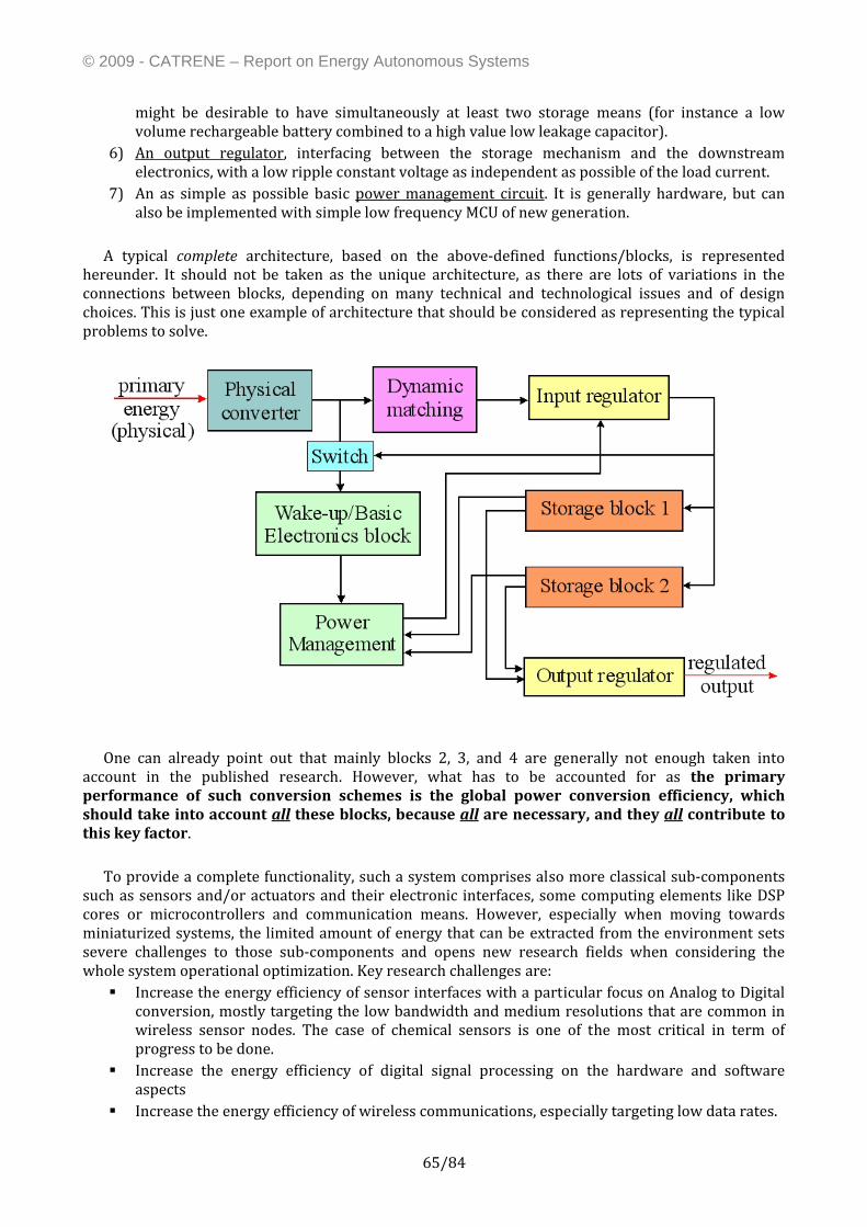
© 2009 - CATRENE – Report on Energy Autonomous Systems
65/84
might be desirable to have simultaneously at least two storage means (for instance a low volume rechargeable battery combined to a high value low leakage capacitor).
6) An output regulator, interfacing between the storage mechanism and the downstream electronics, with a low ripple constant voltage as independent as possible of the load current.
7) An as simple as possible basic power management circuit. It is generally hardware, but can also be implemented with simple low frequency MCU of new generation.
A typical complete architecture, based on the above‐defined functions/blocks, is represented
hereunder. It should not be taken as the unique architecture, as there are lots of variations in the connections between blocks, depending on many technical and technological issues and of design choices. This is just one example of architecture that should be considered as representing the typical problems to solve.
One can already point out that mainly blocks 2, 3, and 4 are generally not enough taken into
account in the published research. However, what has to be accounted for as the primary performance of such conversion schemes is the global power conversion efficiency, which should take into account all these blocks, because all are necessary, and they all contribute to this key factor.
To provide a complete functionality, such a system comprises also more classical sub‐components
such as sensors and/or actuators and their electronic interfaces, some computing elements like DSP cores or microcontrollers and communication means. However, especially when moving towards miniaturized systems, the limited amount of energy that can be extracted from the environment sets severe challenges to those sub‐components and opens new research fields when considering the whole system operational optimization. Key research challenges are:
Increase the energy efficiency of sensor interfaces with a particular focus on Analog to Digital conversion, mostly targeting the low bandwidth and medium resolutions that are common in wireless sensor nodes. The case of chemical sensors is one of the most critical in term of progress to be done.
Increase the energy efficiency of digital signal processing on the hardware and software aspects
Increase the energy efficiency of wireless communications, especially targeting low data rates.
© 2009 - CATRENE – Report on Energy Autonomous Systems
66/84
Develop efficient power down and wake up modes, as those systems might have very low duty cycles. Timing driven wake‐up can be extended to External physical event driven.
Define concepts of energy driven behaviour for such systems. This includes overall energy optimization in nominal situations and fallback strategies in low energy cases.
6.2.3. Recommendations for an efficient research on EAS to address the development of future products
Recommendations for coordinated research and applicative projects
It is recognised worldwide that the development of large arrays of wireless sensors is a key domain
to address fundamental societal needs: Transportation systems: from cars to aeronautics, Medical applications, including eldest people health monitoring Environmental monitoring Civil Engineering structures monitoring and domotics Infrastructures monitoring for security applications Production lines
This explains the huge number of activities, at the research level, and more recently at the
industrial level, around the conversion of environmental energy to electrical energy useful for low power sensors physically distributed in huge volumes.
However, although there are such numerous research activities on Energy Harvesting Systems
(mostly Micro‐Systems) in Europe with valuable results published, it appears also the following facts:
− There is a huge redundancy in some activities (such as piezoelectric bimorphs applied to vibration energy harvesting).
− On another hand, there are “holes” in the research that are anyway considered as crucial to a successful development of future commercial products (for instance, addressing the high dynamic range of incoming energy in some applications, or inventing new metamaterials for improved mechanical to electrical energy conversion efficiencies)
− The research rarely covers (if not at all) the complete functional chain to really address the autonomy (including the possibly long periods where no energy flows in). This point is clearly a limiting factor to the quick introduction of EAS as ready‐to‐market products.
− Some considerations on the reliability of materials and of the heterogeneous integration processes are not assessed. For instance, the bulk thin piezoelectric layers present, in the usual structures (clamped or partly clamped beams), a limited lifetime due to the fabrication process and operational mode.
− Although constant progress is achieved in the fields of low power sensor interfaces, computing and communication, complementary specific researches will be needed to fulfil the application requirements of Energy Autonomous Systems.
These remarks lead to the following recommendations for better synergy between research and
industry actors in application oriented projects:
− Europe should encourage the creation of a few mass‐critical projects on complete Energy Autonomous Systems and Microsystems. The WG is aware that this recommendation might not be applicable immediately because of the contents and planning of the next foreseen CFPs. However, part of these projects (2 or 3 maybe) could be supported through more industrially oriented programmes on a shorter‐term basis, where objectives are driven by applications and
© 2009 - CATRENE – Report on Energy Autonomous Systems
67/84
by a global and coherent system approach to insure the success of the operational products. It should be one main objective of such projects to supply in the end a complete energy autonomous system including an energy harvesting block dedicated to a specific energy incoming flux, going down to packaging issues, and answering to specific domains (for instance: mobile platforms, human body, buildings …)
− Europe should encourage the design of extreme low energy integrated circuits and less big projects in very advanced microelectronic technologies. These technologies down to 22 nanometres or less will be set up by very big worldwide consortium of EU, US and Asian companies. So everybody will access to the same technology. It therefore turns out that the main differentiator for EU companies will be the design and specifically new design techniques for extreme low energy ICs and SoCs. In addition, for many applications in wireless sensor networks, more conservative existing technologies like 90 nanometers perfectly fit the requirements. So for these projects, there is no need for very advanced 22 nm (or less) technologies.
− Europe should also encourage the research and developments on new innovative materials for energy conversion (whether from mechanical to electrical energy, or from thermal to electrical for instance). This encouragement should not only be based on financial support of specific research projects through CFPs, but also by encouraging the creation of European centres of Excellence (maybe 2) dedicated to materials for energy conversion. One can envision that new nanomaterials, new metamaterials, new biology related chemicals … could give a strong impetus to the development of innovative solutions in different domains of applications. For instance, in the medical domain, using biological reactions could lead to the realisation of invivo electronic nano‐sensors and actuators for health monitoring or disabled assistance. These centres should coordinate the activities of its members to avoid double activities, thereby giving more efficient use of invested money, and consequently a lower time to market for European industries.
Recommendations for specific technologically oriented research projects
The WG recommends that, besides more application‐oriented projects (§ 6.2.3.1), more specific
technologically oriented projects dealing with energy functions and blocks for autonomous systems should be supported:
New innovative energy storage technologies for electrical energy:
o Using mechanical schemes (for instance based on MEMS technologies) could give a much longer lifetime than batteries, although at the expense of a lower energy density.
o Chemical schemes should also be diversified. o New capacitor technologies with very low leakage current, using nanotubes or electron‐storing molecules.
New schemes for optical energy conversion. Because optical energy has the highest environmental density, it is worth imagining alternative and possibly cheaper ways than photovoltaic devices. The target is to drastically lower the cost of silicon photovoltaics, while increasing the energy conversion efficiency much over the mean 10% of today.
Metamaterials to generate electrical energy from primary sources of physical energy: o Artificial piezoelectric metamaterials, possibly polymeric to be flexible, with still a high coupling factor k (> 75 %)
o New metameterials for thermal energy flux conversion. Existing materials are very limited in their conversion efficiency, whereas there is a huge potential in various domains of applications, including fundamentally the medical ones.
Investigating biological reactions and their potential use in the medical domain for biologically compliant (invivo) sensors and life‐assisting items.
© 2009 - CATRENE – Report on Energy Autonomous Systems
68/84
Remote powering schemes should not be forgotten, as this might be the ultimate and only solution in some specific cases or domains of applications. Use of RF waves is generally considered a good compromise solution.
Many research efforts are on‐going on the different sub‐components of such a system. Works have now to be enhanced on the whole system: putting the pieces together, and globally optimizing the system. This will require developing "energy aware" design flows.
One could consider that “low power” design today is “business as usual”, but it is not true. “Low power” is quite often related to integrated circuits for portable devices like portable phones or PDAs, so circuits consuming some milliwatts. Such circuits are completely out of scope for wireless sensor networks that require some microwatts or some hundreds of nanowatts, but with very moderate performances in peak frequencies or in computation power. The key is “extreme low energy” circuits and architectures, for which not so much research has been conducted until now. So there is a big shift in design techniques to be capable of designing extreme low energy subthreshold, asynchronous, fault‐tolerant circuits and architectures.
The reliability of materials (such as piezoelectrics) is not well covered. Moreover, activities on this theme generally come late after a material is invented and tested according to the main lines of the products it will be part of. For instance, only one European company is really investing on this action on piezoelectrics since a few years for its own products. Developments of new materials (as cited above) should give the opportunity to start the reliability tests as early as possible, whether at the material level, or at the physical level if the material is not definitely fixed in its constitution.
Micro batteries is a key technology for energy autarkic systems since nearly each system requires an high energy density storage buffer which bridges the time and intensity gap between energy harvesting and energy consumption. In Europe only CEA‐Leti (Grenoble) has a significant activity in the field of batteries based on thin film processing. Currently there are huge activities to strengthen battery development in Europe for hybrid cars or electrical vehicles. Micro batteries for energy autonomous systems will benefit from this materials developments. On the other hand, automotive secondary batteries and micro batteries differ in several ways: Lifetime of autarkic systems will be 20 … 30 years while automotive require 10 years (and perhaps will start with 5 years lifetime). Gravimetric energy density is of less importance in micro systems. Safety is of much lesser concern for small batteries compared with the big ones. Totally different fabrication technologies can be used for micro batteries, for example on a wafer level. Thus we suggest a focused action on micro batteries development based on MEMS and nano technology which takes advantage of these special fabrication opportunities and addresses the typical specifications of energy autarkic micro systems. Another activity should focus on the development of high temperature stable battery materials (especially electrolytes). This is a prerequisite for systems integration into electronics packaging. On the other hand, applications of wireless sensors for automotive and avionic applications will be possible.
Micro Fuel Cells. Until now there was no EC call especially directed towards micro fuel cells or portable fuel cells. Only minor aspects of large fuel cell systems can be applied to micro fuel cells. Nevertheless some micro fuel cell research was embedded as part of power supply technology in a number of projects. Funded research programs with special focus on micro fuel cells are under way on national level in some EC countries (Germany, France, Italy). While internationally most research is aimed on portable micro fuel cells for notebook computers and mobile phones as well as military applications, there are only minor activities for exploitation of ambient fuels in the context of energy autarkic micro systems. Meanwhile Japanese and US companies and institutes are leading the research for portable fuel cells. Based on European strong position in materials and micro system research, a strategic research program should address future micro fuel cell technologies and the use of ambient fuels. All topics described above should be covered in this activity, in particular:
- long term stable PEM or liquid direct fuel cells based on micro technology and deposited ionic membranes and deposited electrodes,
- bio fuel cells (encymatic fuel cell, microbial fuel cell, fuel cells using ambient fuel),
© 2009 - CATRENE – Report on Energy Autonomous Systems
69/84
- autarkic hydrogen generation from ambient sources. - Hybrid systems with electrical storage A great deal of this activity is related to basic research an highly interdisciplinary.
Recommendations for other actions
There is currently a large research effort in the telecommunication field targeting the “wireless sensor networks”; Interactions between those works and the more hardware oriented one’s that are addressed in this report are mandatory. For instance a link has to be established between this working group report and some more telecom‐oriented reports like ongoing "green telecom" white book. Organizing specific common workshops is suggested for instance.
6.2.4. Summary of recommendations, conclusions and perspectives
In conclusion, although the WG does not claim to have covered all information related to research
issues on Energy Autonomous Systems, it has concentrated on the assessment of pragmatic issues related to the coherence of the developments of autonomous functional blocks, and their availability on a medium term in the future products, and also as future products per se. there are effectively good reasons that one day, users (mainly professionals, but maybe also individuals) would buy Micro‐energy blocks like they buy batteries today. Recommendations have been given to address problems pointed out in specific areas of this domain, not enough covered up to now, by hopefully suited lines of actions.
It is also thought that the recommendations for actions developed here above would also largely
benefit to other fields of activities, such as renewable sources of energy from the environment. For instance, there is ongoing research in some laboratories on schemes for wind energy conversion using piezoelectric membranes, with an objective of improving efficiency and reducing maintenance operations costs. In this case, the development of new low cost materials would be applicable. The development of such new materials and systems on a large volume scale would also, by their potential industrial impact, participate to the cost lowering, finally profitable to the diffusion of autonomous Microsystems in Society.
Recommendations on public initiatives 1. Include stronger emphasis on EAS midterm initiatives in ongoing programmes; 2. Diversify in FP7 initiatives EAS themes from “heterogeneous materials” themes
(labonachip, packaging) due to their different perspectives and goals; 3. Enlarge in FP7 themes opportunities for EAS other than ICT (Health,
Nanotechnology, Food & Agriculture, Transport); 4. Promote educational support actions in FP7; 5. Promote exploitation of new knowledge products and best practices
transforming the results of higher education and research activities into commercially exploitable innovation using EC frameworks (such as in Knowledge and Innovation Communities initiatives)
© 2009 - CATRENE – Report on Energy Autonomous Systems
70/84
Recommendations on working methodology 6. Have a systemic approach to EAS architecture where the total efficiency plays the
most important role;
Recommendations for efficient research for applicative projects
7. Focus the research on the overall energy chain related to the operating conditions and environment, addressing the autonomy issue from the application point of view (transportation, environment, production lines etc);
8. More emphasis on the developments on critical operational functions such as the dynamicmatching, input regulator and wakeup blocks (see architecture of previous picture). Reduce overlaps on topics related to energyharvesting principles (i.e. piezoelectric vibration and motion scavenging)
9. Use energyaware electronic EAS system design considering the most recent device trend;
Recommendations for technology oriented research projects 10. Focus the research on new materials for energy harvesting (i.e. piezo meta
materials, nanotechnology based materials); 11. Focus on the reliability and durability of materials.
6.3. Interdisciplinary Education and Training
6.3.1. Ongoing initiatives
EIT
European Institute of Innovation and Technology and its possible role in research, training and innovation for Energy Autonomous Systems
The European Institute of Innovation and Technology (EIT) is a new initiative at the European
Community level to foster the integration of the knowledge triangle: higher education research innovation
The EIT will primarily operate through autonomous partnerships of higher education institutions, research organizations, companies and other stakeholders in the form of sustainable and long‐term self‐supporting strategic networks in the innovation process.
These partnerships will be called Knowledge and Innovation Communities (KICs) and shall be selected by the Governing Board of the EIT (the first KIC is due to start by end of 2009).
KICs will be active in four domains:
a) innovation activities and investments with European added value; b) cutting‐edge and innovation‐driven research in areas of key economic and societal interest; c) education and training activities at masters and doctoral level, in disciplines with the
potential to meet future European socio‐economic;
© 2009 - CATRENE – Report on Energy Autonomous Systems
71/84
d) the dissemination of best practices in the innovation The EIT strategy for a period of seven years will be laid down in a Strategic Innovation Agenda
(SIA) [162]. Considering the broadly multi‐disciplinary aspects involved in the science of Energy Autonomous
Systems (electron and MEMs devices physics for the scavenging, battery chemistry and physics for the storage, power electronics for the power management, low power digital, analogue and RF circuit design, electronic system architecture, to name a few) the education of EAS experts is a daunting task. The creation of a KIC specifically devoted to the field of EAS would answer to three main needs: - establish a credible, multidisciplinary, Europe‐wide education offer in the field - foster a coordinated European research effort in EAS - exploit innovation based on the research activity and the generated human potential to respond to
market and societal needs. This possible initiative is strongly recommended by the working group. As a first step EAS should
be considered in the first draft of the EIT SIA.
STIMESI
The goal of the STIMESI Stimulation Action is to stimulate European universities and research institutes to adopt MEMS and SiP technologies in different ways. First of all the "more experienced" universities active in MEMS design/technology will be stimulated to increase MEMS research activities and design and fabricate more MEMS circuits and SiP components. Secondly it is also the goal to stimulate other universities to actively start teaching/research MEMS/SiP activities. In order to stimulate those universities and research institutes, they must be helped, guided, trained and they must get access to user‐friendly design kits. In order to make sure that the MEMS/SiP technologies can be accessed easily by universities, qualified, robust and user‐friendly design kits and design flows are being developed in the project. The development of robust MEMS design kits must link and include process capability, material properties, statistical and material tolerances. All this information must be integrated into the available MEMS CAD tools.
As soon as the first versions of the design kits become available (second half of first year), training courses will be organised by the foundries. It is very important that trainees when returning home from courses and starting to make home exercises get additional technical support. The foundries organising and lecturing the courses will therefore provide technical assistance to the trainees for a certain time. It is also important that the courses can be used at the university to develop new teaching material so that the MEMS technology can be added in the curricula. A stimulation activity can only be successful with a good dissemination plan. This will include following activities such as a specific WEB site, leaflets and flyers on the different MEMS technologies, promotion of the training courses through various channels, an annual Workshop, etc.
6.3.1. Training in Energy Autonomous Systems
Training in Energy Harvesting and Energy Sources
A conference on Harvesting and Energy Sources, with the focus on applications, is the Nano Power Forum, organized by Darnell Group, which takes place in the United States since 2007. The first European Nano Power Forum will be held in 2009 in the Benelux.
On a more technical level, harvesters and energy sources, as they are fabricated with help of MEMS technologies are dealt with at the PowerMEMS workshop, which rotates between Asia, Europe and US and presents basically university research. Special workshops on micro energy are included in the DTIP conferences (Design, Test, Integration and Packaging of MEMS/MOEMS) held in France and Italy. The small fuel cell conference, organized every year in the US by the knowledge foundation, focuses on
© 2009 - CATRENE – Report on Energy Autonomous Systems
72/84
portable and military fuel cells. In Germany the Haus der Technik organizes a two day workshop on energy harvesting once a year since 2007. At universities the topic of micro energy is most often dealt with in the framework of micro system technology and materials since.
Training in ultra-low energy integrated circuits
Nanoelectronics is nanotechnology applied in the context of electronic circuits and systems. There are several perspectives to the concept of nanoelectronics.
One is the fact that the nanoscale dimensions of nanoelectronic components allow for systems of giga‐scale complexity measured in terms of component on a chip or in a package. This scaling feature and the road to giga‐scale systems can be described in the ‘More Moore’ domain of development [159].
Another is that nanotechnology is very diverse and allows the integration of purely electronic devices with mechanical devices, bio‐devices, chemical devices, etc. Also, digital systems can be combined with analog/RF circuits. This technology fusion can be described in the ‘More than Moore’ domain of development.
A third is that traditional scaling limits in standard CMOS technology are reached during the next decade, calling for fundamentally new nanoscale electronic devices. This development of nanoelectronic components can be denoted the ‘Beyond CMOS’ domain of development
With the advent of nanometric devices, the relevance of leakage power has grown tremendously.
All technology roadmaps, as well as the results from advanced semiconductor labs indicate leakage as the real showstopper for the future generations of nanoelectronic circuits if proper counter‐measures will not be taken. To be successful, and thus leading to the capability of fabricating chips with sub‐65nm technologies, such counter‐measures must be rooted in the design domain, as process improvement will not be sufficient to cope with the increased leakage currents in MOSFETs. In other terms, time has come for considering leakage reduction also a design problem, and not only a technology problem.
Training about low‐power design has been quite successful in the past years. Many courses were
offered, with many attendees, back to the beginning of the nineties. Many conferences and Workshops were also created at this time, like ISLPED and PATMOS. These conferences address many low power topics but still with too few papers about “ultra low energy integrated circuits”. The first “Low‐Power” conferences and workshops were organized around 1993. Before the famous ISLPED (International Symposium on Low Power Electronics and Systems), some U.S. workshops were organized, such as the 1993 Low‐Power Electronics Conference in Arizona and the 1994 Workshop on Low‐Power Design in Napa. These workshops were merged to create the first ISLPED conference that was held in 1995 at Dana Point, CA, and is now regularly organized each year. The conference was held for the first time in Europe in 2000 (Rapallo, Italy), and was held for the first time in Asia (Seoul, Korea) in 2003. In 2001 and 2002, ISLPED was held at Huntington Beach, CA, and Monterey, CA, respectively. Between 2004 and 2008, ISLPED was located in Newport Beach, CA, (2004), San Diego, CA (2005), Lake Tegernsee in Bavaria, Germany (2006), Portland, Oregon (2007) and Bangalore, India, (2008).
Interestingly enough, it was in Europe that the first low‐power workshops appeared, such as
PATMOS (Power and Timing Modeling Optimization and Simulation), organized in 1993 in Montpellier, France, and in 1994 in Barcelona, Spain, with some attendees from the U.S. The PATMOS conference was originally a European project about timing and power modeling (1990–1993); however, it was decided to continue the organization of annual meetings on timing with more information on low‐power issues. This European PATMOS conference was then organized in 1995 at Oldenburg, Germany, Bologna, Italy, Louvain la Neuve, Belgium, Lyngby, Denmark, Kos Island, Greece, Göttingen, Germany, Yverdon, Switzerland, and Sevilla, Spain. It was organized in Torino, Italy, in 2003, in Santorini Island, Greece, in 2004, in Leuven, Belgium, in 2005, in Montpellier, France, in 2006, in Göteborg, Sweden, in 2007 and in Lisbon, Portugal, in 2008. It will be organized in Delft, the
© 2009 - CATRENE – Report on Energy Autonomous Systems
73/84
Netherlands, in 2009. The ASYNC conference is fully dedicated to the design of asynchronous integrated circuits,
including GALS (Globally Asynchronous Locally Synchronous). It is a very selective conference with only one track, with many attendees from the asynchronous community in Europe and US. It was created as ASYNC in 1996 in Aizu, Japan. Between 1997 and 2007, ASYNC was located in Eindhoven, The Netherlands (1997), San Diego, CA (1998), Barcelona, Spain (1999), Israël (2000), Salt Lake City, Utah (2001), Manchester, UK (2002), Vancouver, Canada (2003), Hersonissos, Crete, Greece (2004), New‐York (2005), Grenoble , France (2006) and Berkeley, CA (2007). It will be located in Newcastle, UK, in 2008.
In 1999, the IEEE Alessandro Volta Memorial Workshop on Low‐Power Design (VOLTA’99) was organized in Como, Italy. It was dedicated to low power as well as to recall that A. Volta invented the electric battery 200 years earlier in that town.
A French‐speaking conference, called FTFC (Faible Tension Faible Consommation) was also
organized in Paris every 2 years since 1997, and the sixth edition was organized in May 2007 still in Paris. From this time, it was decided to have this conference every year in different locations, so FTFC 2008 was in Louvain–la‐Neuve, Belgium. The 2009 edition will be located in Neuchâtel, Switzerland and the 2010 edition in Montréal, Canada,
One‐day low‐power workshops were also organized by Dimes Delft University, Netherlands, within
the framework of the ESDLPD (European Low‐Power Initiative for Electronic System Design) from 1997 to 2001. These 1‐day workshops with invited speakers were usually held on the day before or after PATMOS, VOLTA, and ISLPED conferences.
The web site MARLOW (www.lowpower.org) was set up during this MARLOW 2001‐2006 FP6 EU
project (a continuation within FP7 was not accepted). This web site provides many information about low‐power design including material developed within the ESPRIT TARDIS ESD‐L, a low‐power methodology database, selected low power publications, newsletters, low power events and training sessions. INTRALED was also an EU project specifically focused to deliver training in low power design.
CLEAN (controlling leakage power in nanoCMOS SOC's) is an FP6‐IST project, in which the problem
of leakage currents in the upcoming technologies (65nm and below) is addressed. The project is funded by the European Union as a 3 year Integrated Project. Main targets of the CLEAN project are:
− analysis and development of design techniques for leakage reduction − development of EDA tools for leakage aware design using the design techniques − development of EDA tools for high level leakage prediction, supporting leakage aware design
CLEAN is organizing many one day workshops with invited speakers. During 2007, CLEAN was offering 6 workshops in Stresa, Budapest, Göteburg, Munich, Sozopol and Sevilla.
Every year back to 20 years ago, EPFL offer Advanced CMOS IC Design'08in Lausanne, Switzerland. The objective of this one week course provides will provide an in‐depth knowledge of prominent digital design techniques of integrated CMOS circuits and systems including low power design, leakage reduction, low voltage circuits and variation tolerant designs.
Training in Power management
Design of integrated systems and principles of power electronics are basis courses of any engineering curriculum. They are enough to prepare engineers with general competences for the design of power electronics for harvesters. Specific training goes through forums, conferences and tutorials.
© 2009 - CATRENE – Report on Energy Autonomous Systems
74/84
Various international conferences focus on power electronics. IEEE organizes the ECCE (Energy conversion congress and Expo) and the APEC (applied power electronics conference and exposition). The ISSCC (International Solid State Circuit Conference, a high level conference organized by IEEE) also hosts presentations and papers on power management. Power management circuits for harvesters fabricated by MEMS technologies are dealt with also at the PowerMEMS conference which rotates between Asia, Europe and US.
6.3.5. Recommendations − To promote highly interdisciplinary training courses in devices and materials for technology
fusion. Nanotechnology (in a broader sense than nanoelectronics) makes it possible to develop new components which may be used together with electronic components in system design. This includes for instance micromechanical systems, photonic systems, biochemical systems. Also, the combination of digital and analogue/RF circuits may call for combination of different technologies. Together with electronic components, such components open ways to the design of new integrated systems and applications, and research and education is needed concerning such technology fusion options.
− To encourage the creation of courses in “ultra low‐energy” designs (so topics will be a mixed of
sub‐threshold, asynchronous, fault‐tolerant circuits and architectures, technology variations tolerance, power management)
© 2009 - CATRENE – Report on Energy Autonomous Systems
75/84
7. Bibliography
[1] C. Piguet, “Low‐Power electronic design”, CRC press, 2004
[2] B. W. Cook, S. Lanzisera, K. S. Pister, “SoC Issues for RF Smart Dust”, Proceedings of the IEEE, vol. 94, no. 6, pp. 1177‐1194, 2006
[3] M. Pelgrom, R. Roovers, H. Bergveld, “Smart Dust”, in “The New Everyday”, eds Emile Aarts and Stephano Marzano, Koninklijke Philips Electronics N.V. 010 Publishers Rotterdam, 2003,
[4] J.A. Paradiso, T. Starner, “Energy scavenging for mobile and wireless electronics”, IEEE Pervasive Computing, Vol. 4, 1, pp. 18‐27, 2005;
[5] T. Starner, “The challenges of wearable computing: Part 1&2” IEEE Micro, Vol. 21, Issue 4, July‐Aug. 2001;
[6] P. D. Mitcheson, E. Yeatman, G. K. Rao, A. S. Holmes, T, C. Green, “Energy Harvesting from Human and Machine Motion for Wireless Electronic Devices”, Proc. IEEE, vol. 96, no. 9, pp. 1457‐1486, 2008
[7] P. D. Mitcheson T.C. Green, E.M. Yeatman and A.S Holmes, “Architectures for Vibration‐driven Micropower”, J. Microelectromech. Syst., vol. 13, no. 3, pp. 429‐440, 2004
[8] P. D. Mitcheson, E. M. Yeatman, G. Kondala Rao, A. S. Holmes, T. C. Green, “Energy Harvesting From Human and Machine MotionforWireless Electronic Devices”, Proceedings of the IEEE, Vol. 18, 96, No. 9, Sep. 2008
[9] N. S. Hudaka, G. G. Amatucci, “Small‐scale energy harvesting through thermoelectric, vibration, and radiofrequency power conversion”, JOURNAL OF APPLIED PHYSICS 103, 101301, 2008
[10] T. Sterken, P. Fiorini, K. Baert, R. Puers, G. Borghs. An electret‐based electrostatic micro‐generator. Proceedings of the 12th Int. Conf. On Solid‐State Sensors, Actuators and Microsystems Transducers 2003, pp. 1291‐1294.
[11] P. Miao, P. D. Mitcheson, A. S. Holmes, E. M. Yeatman, T. C. Green, B. H. Stark. MEMS inertial power generators for biomedical applications. Microsyst Technology 12, pp. 1079–1083, 2006.
[12] G. Despesse, J.J. Chaillout, T. Jager, F. Cardot, A. Hoogerwerf. Innovative Structure for Mechanical Energy Harvesting. Int. Conf. on Solid‐State Sensors, Actuators and Microsystems, Transducers 2007, pp. 895 – 898, 2007.
[13] P. Glynne‐Jones, S.P. Beeby, E.P. James , N.M. White. The Modelling of a Piezoelectric Vibration Powered Generator for Microsystems. Int. Conf. On Solid‐State Sensors, Actuators and Microsystems, Transducers 2001, pp.46‐49,2001.
[14] M. Marzencki, Y. Ammar, S. Basrour. Integrated Power Harvesting System Including a MEMS Generator and a Power Management Circuit, Int. Conf. on Solid‐State Sensors, Actuators and Microsystems, 2007. Transducers 2007, pp. 887 – 890, 2007.
[15] R. Elfrink, T. M. Kamel, M. Goedbloed, S. Matova, D. Hohlfeld, R. van Schaijk, R. Vullers, “Vibration Energy Harvesting With Aluminum Nitride‐Based Piezoelectric Devices”, Proc. of the PowerMEMS Int. Workshop, Sendai, Nov 10‐11 2008, pp 249 – 252.
[16] Neil N. H. Ching, H. Y. Wong, Wen J. Li, Philip H. W. Leong, Zhiyu Wen, “A laser‐micromachined multi‐modal resonating power transducer for wireless sensing systems” Sensors and Actuators A: Physical, Volumes 9798, 1 April 2002, Pages 685690
[17] http://www.perpetuum.co.uk
© 2009 - CATRENE – Report on Energy Autonomous Systems
76/84
[18] D. Spreemann, Y. Manoli, B. Folkmer, D. Mintenbeck. Non‐ resonant vibration conversion. Journal of Micromechanics and Microengineering Vol.16. pp. S169‐173, 2006.
[19] T. Sterken, P. Fiorini, R. Puers. “Motion‐based generators for industrial applications” Proceedings of the International Conference on Design, Test, Integration and Packaging of MEMS/MOEMS ,pp. 328‐331,200
[20] S. P. Beeby, R. N. Torah, M.J. Tudor, P. Glynne‐Jones, T. O’Donnell, C. R. Saha, S. Roy, “A micro electromagnetic generator for vibration energy harvesting”, J. Micromech. Microeng., 2007, vol .17, pp. 1257‐1265
[21] M. Renaud, T. Sterken, A. Schmitz, P. Fiorini, C. Van Hoof, R. Puers, “Piezoelectric Harvesters and MEMS Technology: Fabrication, Modeling and Measurements”, Int. Conf. On Solid‐State Sensors, Actuators and Microsystems, 2007. TRANSDUCERS 2007. 10‐14 June 2007, pp. 891 – 894
[22] G. Snyder and E. Toberer, “Complex thermoelectric materials”, Nature Materials, Vol. 7, no. 2, February 2008, pp. 105‐114
[23] Z. Wang, V. Leonov, P. Fiorini, C. Van Hoof, “Micromachined thermopiles for energy harvesting on human body”, Int. Conf. On Solid‐State Sensors, Actuators and Microsystems TRANSDUCERS 2007. 10‐14 June 2007, pp. 911‐914
[24] http://www.poweredbythermolife.com
[25] http://www.nextreme.com/pages/products/teg.html
[26] http://www.micropelt.com/down/datasheet_mpg_d602_d751.pdf
[27] A. Hagfeldt and M. Grätzel, “Molecular Photovoltaics”, Acc. Chem. Res., vol. 33, 2000, pp. 269‐277
[28] S.E. Shaheen, C.J. Brabec, N.S. Sariciftci, F. Padinger, T. Fromherz, J.C. Hummelen, “2.5% Efficient Organic Plastic Solar Cells”, Appl.Phys.Lett. vol. 78, 2001, p. 841
[29] K. Bücher, “Site dependence of the energy collection of PV modules”, Solar Energy Materials and Solar Cells, vol. 47, no. 1, 1997, pp. 85–94
[30] http://www.powercastco.com
[31] R.J.M Vullers, H. J. Visser, B. Op het Veld, V. Pop, “RF Harvesting Using Antenna Structures On Foil”, Proc. of PowerMEMS 2008, Sendai, Japan, 10‐11 Nov 2008, pp 209‐212.
[32] J. Fildes, “Wireless energy promise powers up,” BBC News, http:// news.bbc.co.uk/2/hi/technology/6725955.stm.
[33] M. Takamiya, T. Sekitani, Y. Miyamoto, Y. Noguchi, H. Kawaguchi, T. Someya, T. Sakurai, “Design Solutions for a Multi‐Object Wireless Power Transmission Sheet Based on Plastic Switches,” 2007 IEEE Int. Solid‐State Circuits Conf. (ISSCC) Dig. Tech. Pap. pp. 352,609, 2007
[34] C. van Hoof, “Micro‐Power Generation using Thermal and Vibrational Energy Scavengers. 12 Years of Energy Harvesting – An overview”, presented at 2008 IEEE Int. Solid‐State Circ. Conf. (ISSCC), 2008
[35] J. B. Bates, N. J. Dudney, B. Neudecker, A. Ueda, C. D. Evans, “Thin‐film lithium and lithium‐ion batteries,” Solid State Ionics, vol. 135, 2000, pp. 33–45
[36] C. Brand, “A micro battery for low power applications”, in Proc. of nanoPower Forum 2007, San Jose, USA, June 4‐6th, 2007
[37] M. Nathan, D. Golodnitsky, V. Yufit, E. Strauss, T. Ripenbein, I. Shechtman, S. Menkin, E. Peled, “Three dimensional (3d) thin film micro batteries,” in Proc. of Symposium on Design, Test, Integration, Packaging of MEMS/MOEMS, 2005
© 2009 - CATRENE – Report on Energy Autonomous Systems
77/84
[38] R. Hahn, “Battery, especially a microbattery, and the production thereof using wafer‐level technology”, WO2005036689 (A3), WO2005036689 (A2), EP1673834 (A3), EP1673834 (A0), DE10346310 (A1), 2006
[39] R. Hahn, “Autonomous energy supply for electronic grains and wireless sensors,” Frequenz, no. 3‐4, pp. 87 – 91, 2 2004.
[40] R. Hahn, K. Marquardt*, T. Luger*, H. Reichl, “Assembly of Wafer Level Secondary Batteries”, International Symposium PowerMEMS, Tokyo, Nov. 28‐30, 2005
[41] K. Marquardt, R. Hahn, T. Luger, H. Reichl, Assembly of and hermetic Encapsulation of wafer level secondary batteries, MEMS2006 Istanbul, 22.‐26. Jan.2006, pp. 954‐ 957
[42] http://news‐service.stanford.edu/news/2008/january9/nanowire‐010908.html
[43] IEEE 802.15.4, IEEE Standard for Information Technology, 2006, http://standards.ieee.org/getieee802/download/802.15.4‐2006.pdf
[44] IEEE 802.15.4a, IEEE Standard for Information Technology, 2007, http://standards.ieee.org/getieee802/download/802.15.4a‐2007.pdf
[45] http://www.wibree.com
[46] C. Bernier, et al., “An Ultra low power 130nm CMOS direct conversion transceiver for IEEE802.15.4”, in Proc. of IEEE 2008 Radio Frequency Integrated Circuit (RFIC) Symposium, 15‐17 June 2008, pp. 273‐276
[47] J. Ryckaert et al., “A 16mA UWB 3‐5GHz 20 Mpulses/s quadrature analog correlation receiver in 0.18µm CMOS”, 2006 IEEE Int. Solid‐State Circ. Conf. (ISSCC) Dig. Tech. Pap., pp. 368‐377, 5‐9 February 2006, San Francisco, (USA)
[48] L. Stoica, S. Tiuraniemi, I. Oppermann, H. Repo, “An ultra wideband low complexity circuit transceiver architecture for sensor networks” in Proc. of 2005 IEEE Int. Symposium on Circuits and Systems (ISCAS), 23‐26 May 2005, vol. 1, pp. 364‐367
[49] J. Gerrits and al., “Principles and Limitations of Ultra‐Wideband FM Communications Systems” in EURASIP Journal on Applied Signal Processing, vol. 2005, no. 3, pp. 382–396.
[50] I. D. O’Donnell, R. W. Brodersen, “An Ultra‐Wideband Transceiver Architecture for Low Power, Low Rate, Wireless Systems”, in IEEE Trans. on Vehicular Technology, vol. 54, no. 5, Sept. 2005, pp. 1623‐1631
[51] http://focus.ti.com/docs/prod/folders/print/cc1020.html
[52] V. Peiris et al., “A 1V 433/868 MHz 25 kb/s‐FSK 2 kb/s‐OOK RF transceiver SoC in standard digital 0.18μm CMOS“ in 2005 IEEE Solid‐State Circ. Conf. (ISSCC) Dig. Tech. Pap., 6‐10 Feb. 2005, pp. 258–259
[53] S. Lindfors, A. Pärssinen, K. Halonen, “A 3‐V 230‐MHz CMOS Decimation Subsampler” IEEE Trans. on Circuits and Systems II: Analog and Digital Signal Processing, vol. 50, no. 3, pp. 105‐117, March 2003
[54] H. Pekau, J. Haslett, “A 2.4 GHz CMOS Sub‐Sampling Mixer With Integrated Filtering”, IEEE Journal of Solid‐State Circuits, vol. 40, no. 11, pp. 2159‐2166, November 2005
[55] M. B. Nejad et al., "An Innovative Semi‐UWB Passive Transponder for Wireless Sensor and RFID Applications", In Proc. of First International Conference on Industrial and Information Systems, pp. 310‐315, 2006
[56] B. Otis, Y.H. Chee, J. Rabaey, “A 400μW‐RX, 1.6mW‐TX Super‐Regenerative Transceiver for Wireless Sensor Networks” in 2005 IEEE Solid‐State Circ. Conf. (ISSCC) Dig. Tech. Pap., 6‐10 Feb. 2005, pp. 396‐397
[57] K. Martinez, R. Ong, J. K. Hart, and J. Stefanov, “GLAC‐SWEB: a sensor web for glaciers”, in First European Workshop on Wireless Sensor Networks, 2004
© 2009 - CATRENE – Report on Energy Autonomous Systems
78/84
[58] R. Riem‐Vis, “Minimum sideband noise in oscillators”, in Workshop on Applications of Mobile Embedded Systems, 2004.
[59] F. Michahelles, P. Matter, A. Schmidt, and B. Schiele, “Applying wearable sensors to avalanche rescue”, in Computers and Graphics, vol. 27, no. 6, 2003, pp. 839–847.
[60] E. Lopelli, J. D. van der Tang, A. H. M. van Roermund, “A 1 mA Ultra‐Low‐Power FHSS TX front‐end utilizing direct modulation with digital pre‐distortion”, in IEEE Journal of Solid‐State Circuits, vol. 42, no. 10, October 2007, pp. 2212‐2223
[61] N. Pletcher, S. Gambini, J. Rabaey, “A 2GHz 52μW Wake‐Up Receiver with ‐72dBm Sensitivity Using Uncertain‐IF Architecture”, in 2008 IEEE Solid‐State Circ. Conf. (ISSCC) Dig. Tech. Pap., Feb. 2008, pp. 524‐525
[62] V. P. Petkov, B. E. Boser, “A fourth‐order Sigma/Delta interface for micromachined inertial sensors”, IEEE Journal of Solid‐State Circuits, vol. 40, no. 8, Aug. 2005, pp. 1602–1609
[63] F. Gayral, E. Delevoye, C. Condemine, E. Colinet, M. Beranger, F. Mieyeville, F. Gaffiot, F., “A 100Hz 5nT/Hz Low‐Pass ΔΣ Servo‐Controlled Microfluxgate Magnetometer Using Pulsed Excitation”, 2007 IEEE Solid‐State Circ. Conf. (ISSCC) Dig. Tech. Pap., 11‐15 Feb. 2007 pp. 384 ‐ 610
[64] C. Condemine, N. Delorme, J. Soen, J. Durupt, J.‐P. Blanc, M. Belleville, A. Besancon‐Voda, “A 0.8 mA 50 Hz 15 b SNDR ΔΣ closed‐loop 10g accelerometer using an 8th‐order digital compensator”, 2005 IEEE Solid‐State Circ. Conf. (ISSCC) Dig. Tech. Pap., 6‐10 Feb. 2005 pp. 248 ‐ 249
[65] H. Kulah et al., “A Multistep Electromechanical ΔΣ Converter for Microg Capacitive Accelerometers”, 2003 IEEE Solid‐State Circ. Conf. (ISSCC) Dig. Tech. Pap., Feb., 2003, pp. 202, 488
[66] R. H. Walden, “Analog‐to‐digital converter survey and analysis “ IEEE Journal on Selected Areas in Communications, vol. 17, no. 4, pp. 539‐550, Apr 1999
[67] B. Le, T. W. Rondeau, J. H. Reed, C. W. Bostian, “Analog‐to‐digital converters”, IEEE Signal Processing Magazine, vol. 22, no. 6, Nov. 2005, pp. 69‐ 77
[68] A. Varzaghani, C.‐K.K. Yang, “A 600‐MS/s 5‐bit pipeline A/D converter using digital reference calibration”, IEEE Journal of Solid‐State Circuits, vol. 41, no. 2, Feb. 2006, pp. 310 ‐ 319
[69] B. Murmann, "ADC Performance Survey 1997‐2008," [Online]. Available: http://www.stanford.edu/~murmann/adcsurvey.html.
[70] S. Rabii, B. A. Wooley, “A 1.8‐V digital‐audio sigma‐delta modulator in 0.8‐μm CMOS”, IEEE Journal of Solid‐State Circuits, vol. 32, no. 6, Jun. 1997, pp. 783‐796
[71] W. Sansen, “Analog design essentials”, Springer, Dordrecht (NL), 2006
[72] J. Craninckx, G. Van der Plas, “A 65fJ/Conversion‐Step 0‐to‐50MS/s 0‐to‐0.7mW 9b Charge‐Sharing SAR ADC in 90nm Digital CMOS” 2007 IEEE Int. Solid‐State Circ. Conf. (ISSCC) Dig. Tech. Pap., 11‐15 Feb. 2007, pp. 246 ‐ 600
[73] K. Uyttenhove, M. S. J. Steyaert, “Speed‐power‐accuracy tradeoff in high‐speed CMOS ADCs” IEEE Transactions on Circuits and Systems II: Analog and Digital Signal Processing, vol. 49, no. 4, Apr. 2002, pp. 280‐287
[74] V. Giannini, P. Nuzzo, V. Chironi, A. Baschirotto, G. Van der Plas, J. Craninckx, “An 820μW 9b 40MS/s Noise‐Tolerant Dynamic‐SAR ADC in 90nm Digital CMOS”, 2008 Int. Solid‐State Circ. Conf. (ISSCC) Dig. Tech. Pap., 3‐7 Feb. 2008, pp. 238 ‐ 610
[75] H. C. Hong, G. M. Lee “A 65‐fJ/Conversion‐Step 0.9‐V 200‐kS/s Rail‐to‐Rail 8‐bit Successive Approximation ADC”, IEEE Journal of Solid‐State Circuits, vol. 42, no. 10, Oct. 2007, pp. 2161‐2168.
© 2009 - CATRENE – Report on Energy Autonomous Systems
79/84
[76] A. Agnes, E. Bonizzoni, P. Malcovati, F. Maloberti: “A 9.4‐ENOB 1V 3.8μW 100kS/s SAR ADC with Time‐Domain Comparator”, 2008 Int. Solid‐State Circ. Conf. (ISSCC) Dig. Tech. Pap., 3‐7 Feb. 2008, pp. 246 ‐ 610
[77] D. J. Kinniment, A. V. Yakovlev, F. Xia, B. Gao, “Towards Asynchronous A/D conversion”, in Proc. of the 4th International Symposium on Advanced Research in Asynchronous Circuits and Systems (ASYNC’98), San Diego, CA, Mar‐Apr 1998, p. 206
[78] N. Sayiner, H. V. Sorensen, T. R. Viswanathan, “A level‐crossing sampling scheme for A/D conversion”, IEEE Transactions on Circuits and Systems II: Analog and Digital Signal Processing, vol. 43, no. 4, Apr. 96, pp. 335‐339
[79] L. Alacoque, M. Renaudin, S. Nicolle, "An Irregular Sampling and Local Quantification Scheme A‐D Converter", IEE Electronics Letters, vol. 39, no. 3, pp. 263‐264, Feb. 2003
[80] E. Allier, G. Sicard, L. Fesquet, M. Renaudin, “A new class of Asynchronous A/D converters based on time quantization”, in Proc. of the 9th International Symposium on Asynchronous Circuits and Systems (ASYNC’03), Vancouver, Canada, 2003, p. 196
[81] F. Aeschlimann, E. Allier, L. Fesquet, M. Renauding, “Asynchronous FIR filters: Towards a new digital processing chain”, in Proc. of the 10th International Symposium on Asynchronous Circuits and Systems (ASYNC’04), pp. 198‐206
[82] Y. W. Li, K. L. Shepard, Y. P. Tsividis, “Continuous Time Digital Processor”, in Proc. of the 11th International Symposium on Asynchronous Circuits and Systems (ASYNC’05), pp. 138‐143
[83] J. Kim, S. Cho, “A Time‐Based Analog‐to‐Digital Converter Using a Multi‐Phase Voltage‐Controlled Oscillator,” in Proc. of IEEE International Symposium on Circuits and Systems (ISCAS’06), pp. 3934–3937, May 2006.
[84] U. Wismar, D, Wisland, P. Andreani, “A 0.2V, 7.5 μW, 20 kHz ΣΔ modulator with 69 dB SNR in 90 nm CMOS”, in Proc. of the 33rd European Solid State Circuits Conference (ESSCIRC), 2007, 11‐13 Sept. 2007, pp. 206 – 209
[85] A. Selvakumar, N. Yazdi, K. Najafi, “Low power, wide range threshold acceleration sensing system”, in Proc. of the IEEE Ninth Annual International Workshop on Micro Electro Mechanical Systems (MEMS '96), 11‐15 Feb. 1996, pp. 186 ‐ 191
[86] http://inst.eecs.berkeley.edu/~n225c/sp08/arch_design.doc.
[87] I. Verbauwhede, C. Piguet, P. Schaumont, B. Kienhuis, “Architectures and Design Techniques for Energy‐Efficient Embedded DSP and Multimedia Processing”, Embedded Tutorial, Proc. DATE’04, Paris, February 16‐20, 2004, Paper 7G, pp. 988‐995.
[88] http://bwrc.eecs.berkeley.edu/Classes/EE225C/Lectures/lec3_soc.ppt
[89] G. Frantz, “Digital Signal Processor Trends”, IEEE Micro, Nov.‐Dec. 2000, pp. 52‐59.
[90] P. Pirsch, H‐J. Stolberg, “VLSI Architectures for Multimedia”, in Proc. of the 24th European Solid State Circuits Conference (ESSCIRC), 1998, The Hague, The Netherlands, 22‐24 Sep. 1998, pp. 3‐11.
[91] I. Verbauwhede, C. Piguet, P. Schaumont, B. Kienhuis, “Architectures and Design Techniques for Energy‐Efficient Embedded DSP and Multimedia Processing”, Embedded Tutorial, Proc. DATE’04, Paris, February 16‐20, 2004, Paper 7G, pp. 988‐995
[92] R. David, et al, “Low‐Power Reconfigurable Processors”, Chapter 20 in “Low Power Electronics Design”, edited by C. Piguet, CRC Press, November 2004.
[93] “DSP Blocks in Stratix II devices”, Altera Corp. data sheet, February 2004
[94] F. Rampogna et al., “Magic, a Low‐Power, re‐configurable DSP”, Chapter 21 in “Low Power Electronics Design”, edited by C. Piguet, CRC Press, November 2004.
© 2009 - CATRENE – Report on Energy Autonomous Systems
80/84
[95] C. Arm, J.‐M. Masgonty, M. Morgan, C. Piguet, P.‐D. Pfister, F. Rampogna, P. Volet; “Low‐Power Quad‐MAC 170 μW/MHz 1.0 V MACGIC DSP Core”, in Proc. of the 32nd European Solid State Circuits Conference (ESSCIRC),2006, 19‐22 Sep. 2006, Montreux, Switzerland, pp. 223‐226
[96] Ph. Mosch et al. “A 72μW, 50 MOPS, 1V DSP for a hearing aid chip set”, 2000 IEEE Int. Solid‐State Circ. Conf. (ISSCC) Dig. Tech. Pap., Feb. 7‐9 2000, pp. 238‐239
[97] T. R. Halfhill, “PicoChip makes a Big MAC”, Microprocessor Report, October 14, 2003.
[98] Jan M. Rabaey, “Reconfigurable Processing: The solution to Low‐Power programmable DSP”, International Conf. on Acoustics, Speech and Signal Processing (ICASSP), April 1997.
[99] A. Abnous, J. Rabaey, “Ultra‐Low‐Power Domain‐Specific Multimedia Processors”, VLSI Signal Processing IX. IEEE Press, Ed. W. Burleson, November 1996, pp. 459‐486
[100] K. Roy, S. Mukhopadhyay, H. Mahmoodi‐Meimand, “Leakage Current Mechanisms and Leakage Reduction Techniques in Deep‐Submicrometer CMOS Circuits”, Proc. of the IEEE, vol. 91, no.2, 2003, pp. 305‐327.
[101] C. Piguet, C. Schuster, J‐L. Nagel, “Optimizing Architecture Activity and Logic Depth for Static and Dynamic Power Reduction”, Proc. of the 2nd Northeast Workshop on Circuits and Systems – NewCAS’04, June 20‐23, 2004, Montréal, Canada
[102] C. Schuster, J.‐L. Nagel, C. Piguet, P.‐A. Farine, “Leakage reduction at the architectural level and its application to 16 bit multiplier architectures”, PATMOS ’04, Santorini Island, Greece, September 15‐17, 2004
[103] C. Schuster, C. Piguet, J‐L. Nagel, P‐A. Farine, “An Architecture Design Methodology for Minimal Total Power Consumption at Fixed Vdd and Vth”, Journal of Low‐Power Electronics (JOLPE), vol. 1, no. 1, April 2005, pp. 1‐8.
[104] C. Schuster, J‐L. Nagel, C. Piguet, P‐A. Farine, “Architectural and Technology Influence on the Optimal Total Power Consumption”, DATE 2006, Munchen, March 6‐10, 2006
[105] C. Piguet, C. Schuster, J‐L. Nagel, ”Static and Dynamic Power Reduction by Architecture Selection”, invited paper at PATMOS’06, Montpellier, France September 13‐15, 2006, pp. 659‐668.
[106] E. Vittoz, “Weak Inversion for Ultimate Low‐Power Logic”, Chapter 16, in “Low‐Power Electronics Design”, edited by C. Piguet, CRC Press, November 2004
[107] R. M. Swanson, J. D. Meindl, "Ion‐implanted complementary MOS transistors in low‐voltage circuits", IEEE Journal of Solid‐State Circuits, vol. SC‐7, April 1972, pp.146‐153.
[108] H. Soeleman, K. Roy, “Ultra‐low power digital subthreshold logic circuits", Proc. Of International Symposium on Low Power Electronics and Design, pp.94‐96, 1999.
[109] J. Burr, J. Shott, "A 200 mV self‐testing encoder/decoder using Stanford ultra‐low‐power CMOS", 1994 IEEE Int. Solid‐State Circ. Conf. (ISSCC) Dig. Tech. Pap., 1994, pp. 84‐85,316.
[110] M. Miyazaki et al., "A 175 mV multiply‐accumulator unit using an adaptive supply and body bias (ASB) architecture", 2002 IEEE Int. Solid‐State Circ. Conf. (ISSCC) Dig. Tech. Pap., 2002, pp. 58‐59,444.
[111] E. Vittoz, J. Fellrath, "CMOS analog integrated circuits based on weak inversion operation", IEEE Journal of Solid‐State Circuits, vol. SC‐12, June 1977, pp. 224‐231.
[112] E. Vittoz, "Micropower Techniques", Design of VLSI Circuits for Telecommunications and Signal Processing, Chapter 3, Editors J. Franca and Y. Tsividis, Prentice‐Hall, 1994.
[113] E. Vittoz, “Very low power circuit design: fundamentals and limits", in Proc. of IEEE International Symposium on Circuits and Systems (ISCAS), 1993, vol.2, pp. 1439‐1442.
© 2009 - CATRENE – Report on Energy Autonomous Systems
81/84
[114] C. Enz, F. Krummenacher, E. Vittoz, "An analytical MOS transistor model valid in all regions of operation and dedicated to low‐voltage and low‐current applications", Analog Integrated Circuits and Signal Processing, vol.8, July 1995, pp. 83‐114.
[115] S. Hanson, B. Zhai, D. Blaauw, D. Sylvester, A. Bryant, X. Wang, “Energy Optimality and Variability in Subthreshold Design”, International Symposium on Low Power Electronics and Design (ISLPED), 2006, pp. 363‐365.
[116] B. Zhai, B., D. Blaauw, D. Sylvester, K. Flautner,. “Theoretical and Practical Limits of Dynamic Voltage Scaling”, Design Automation Conference, 2004 , pp. 868‐873.
[117] A. Wang, A. Chandrakasan, S. Kosonocky, “Optimal Supply and Threshold Scaling for Sub‐threshold CMOS Circuits,” Symposium on VLSI, pp. 7‐11, April 2002.
[118] B. Zhai, et al., “A 2.60pJ/Inst Subthreshold Sensor Processor for Optimal Energy Efficiency,” VLSI Ckts Symp, 2006.
[119] N. Verma, A. P. Chandrakasan, “A 65nm 8T Sub‐Vt SRAM Employing Sense‐Amplifier Redundancy”, 2007 IEEE Int. Solid‐State Circ. Conf. (ISSCC) Dig. Tech. Pap., Feb. 2007, pp. 328‐329, Feb. 2007.
[120] J. Kwong, et. al., “A 65nm Sub‐Vt Microcontroller with Integrated SRAM and Switched‐Capacitor DC‐DC Converter,” 2008 IEEE Int. Solid‐State Circ. Conf. (ISSCC) Dig. Tech. Pap., Feb. 2008, pp. 318‐319
[121] S. B. Furber, "Asynchronous Design for Low Power", Chapter 7, NATO ASI Book on Low‐Power, 1997
[122] S. B. Furber et al. "The Design and Evaluation of an Asynchronous Microprocessor", in Proc. of ICCD'94, Boston, MA, October 10‐12, 1994, pp. 217‐220.
[123] S. B. Furber et al. "AMULET1, A Micropipelined ARM", in Proc. of CompCon'94, San Francisco, March 1994.
[124] C. Piguet et al., “Low‐Power Digital Design and CAD Tools”, invited talk, Colloque CAO de circuits intégrés et systèmes, Aix en Provence, 10‐12 May 1999.
[125] C. Piguet, “Low‐Power Issues for SoCs”, DATE 2001, Münich, 13‐16 mars 2001, pp. 488‐490
[126] H. van Gageldonk et al., "An asynchronous Low‐Power 80C51 Microcontroller", in Proc. of the 4th International Symposium on Advanced Research in Asynchronous Circuits and Systems (ASYNC’98), San Diego, CA, March 29‐31, 1998, pp. 96‐107.
[127] L. S. Nielsen, J. Sparsoe, “Designing Asynchronous Circuits for Low Power: An IFIR Filter Bank for a Digital Hearing Aid”, Proceeding of the IEEE, vol. 87, no 2, Feb. 1999, pp. 268‐281
[128] M. Renaudin, P. Vivet, F. Robin, “ASPRO‐216: A Standard‐Cell Q.D.I. 16‐Bit RISC Asynchronous Microprocessor”, in Proc. of the 4th International Symposium on Advanced Research in Asynchronous Circuits and Systems (ASYNC’98), San Diego, CA, Mar‐Apr 1998, pp. 22‐31
[129] K. Slimani, Y. Rémond, G. Sicard, M. Renaudin, “TAST Profiler and Low Energy Asynchronous Design Methodology”, PATMOS 2004, pp. 268‐277
[130] M. Renaudin, G. F. Bouesse, Ph. Proust, J. P. Tual, L. Sourgen, F. Germain, “High Security Smartcards”, DATE 2004, pp. 228‐233
[131] J‐L. Nagel, C. Piguet, "Low‐Power Design of Asynchronous Microprocessors", PATMOS'98, October 6‐8, 1998, Copenhagen, Denmark.
[132] M. Krstic, E. Grass, F. K. Gurkaynak, P. Vivet, “Globally Asynchronous, Locally Synchronous Circuits: Overview and Outlook”, IEEE Design & Test of Computers, vol. 24, no. 5, Sept.‐Oct. 2007, pp. 430 ‐ 441
© 2009 - CATRENE – Report on Energy Autonomous Systems
82/84
[133] D. Lattard, E. Beigne, C. Bernard, C. Bour, F. Clermidy Y. Durand, J. Durupt, D. Varreau, P. Vivet, P. Penard, A. Bouttier, F. Berens, “A Telecom Baseband Circuit based on an Asynchronous Network‐on‐Chip”, 2007 IEEE Int. Solid‐State Circ. Conf. (ISSCC) Dig. Tech. Pap., Feb. 2007, pp. 258‐259
[134] Y. Thonnart, E. Beigné, A. Valentian, P. Vivet, “Automatic Power Regulation based on an Asynchronous Activity Detection and its Application to ANOC Node Leakage Reduction”, in Proc. of the 14th IEEE Int. Symposium on Asynchronous Circuits and Systems (ASYNC'2008), New‐Castle, UK, April 2008, pp. 48‐57
[135] D. Ernst, et al., “Razor: A Low‐Power Pipeline Based on Circuit‐Level Timing Speculation,” in Proc. IEEE/ACM Intl. Symp. Microarchitecture (MICRO‐36), Dec. 2003, pp. 7‐18.
[136] D. Blaauw, et al., “Razor II: In Situ Error Detection and Correction for PVT and SER Tolerance,” 2008 IEEE Int. Solid‐State Circ. Conf. (ISSCC) Dig. Tech. Pap., Feb. 2008, Feb. 2008, pp. 400‐401.
[137] S. Das, et al., “A Self‐Tuning DVS Processor Using Delay‐Error Detection and Correction,” IEEE Journal of Solid‐State Circuits, pp. 792‐804, Apr. 2006
[138] K. A. Bowman, et al., “Energy‐Efficient and Metastability‐Immune Timing‐Error Detection and Instruction‐Replay‐Based Recovery Circuits for Dynamic‐Variation Tolerance,”, 2008 IEEE Int. Solid‐State Circ. Conf. (ISSCC) Dig. Tech. Pap., Feb. 2008, pp. 402‐403.
[139] K. V. Palem, “Proof as experiment: probabilistic algorithms from a thermodynamic perspective”, in Proc. Intl. Symposium on Verification (Theory and Practice), Taormina, Italy, June 2003
[140] K. V. Palem, “Energy aware computing through probabilistic switching: a study of limits”, IEEE Transactions on Computers, vol. 54, no.9, pp.1123–1137, 2005.
[141] K. V. Palem, L. N. Chakrapani, B. E. S. Akgul, P. Korkmaz, “Realizing ultra‐low energy application specific soc architectures through novel probabilistic CMOS (PCMOS) technology”, in Proc. of The International Conference on Solid State Devices and Materials (SSDM), Sept. 2005.
[142] H. Nagayoshi, T. Kajikawa, T. Sugiyama, "Comparison of maximum power point control methods for thermoelectric power generator", Proceedings of IEEE 21st International Conference on Thermoelectronics, 2002, pp. 450‐453.
[143] D. Shmilovitz, "On the control of photovoltaic maximum power point tracker via output parameters," Electric Power Applications, IEE Proceedings ‐ ,52, pp. 239‐248, 2005.
[144] J. F. Dickson, “On‐chip high‐voltage generation in MNOS integrated circuits using an improved voltage multiplier technique”, IEEE Journal of Solid‐State Circuits, vol. 11, no. 3 pp. 374‐378, June 1976.
[145] I. Doms, P. Merken, C. Van Hoof, “Comparison of DC‐DC‐converter Architectures of Power Management Circuits for Thermoelectric Generators”, Proceedings of 2007 European Conference on Power Electronics and Applications, pp. 1‐5.
[146] H. Shao, C‐Y. Tsui, W‐H. Ki, “An Inductor‐less Micro Solar Power Management System Design for Energy Harvesting Applications”, Proceedings of ISCAS 2007, pp. 1353‐1356
[147] N. Guilar, A. Chen, T. Kleeburg, R. Amirtharajah, “Integrated solar energy harvesting and storage”, in Proceedings of the 2006 International Symposium on Low Power Electronics and Design (Tegernsee, Bavaria, Germany, October 04 ‐ 06, 2006).
[148] D. A. Bennett, R. H. Selfridge, J. N. Harb, D. T. A. Comer, “A control circuit for a microsensor hybrid power supply”, IEEE Transactions on Industrial Electronics, vol. 51, no. 1, Feb. 2004
[149] http://www.truesolarautonomy.com
© 2009 - CATRENE – Report on Energy Autonomous Systems
83/84
[150] T. Torfs, V. Leonov, C. Van Hoof, B. Gyselinckx, “Body‐Heat Powered Autonomous Pulse Oximeter”, 5th IEEE Conference on Sensors, 2006, pp. 427‐430
[151] L. Mateu, FhG, PowerMEMS 2007, Power management for energy harvesting applications (P. Spies, M. Pollak, G. Rohmer) – http://www.smart‐power.fraunhofer.de
[152] H. Lhermet, C. Condemine, M. Plissonnier, R. Salot, P. Audebert, M. Rosset, “Efficient Power Management Circuit: From Thermal Energy Harvesting to Above‐IC Microbattery Energy Storage”, IEEE Journal of Solid‐State Circuits, vol. 43, no. 1, Jan. 2008, pp. 246‐255
[153] I. Doms, P. Merken, R. Mertens, C. Van Hoof, “A Capacitive Power‐Management Circuit for Micropower Thermoelectric Generators with a 2.1μW Controller”, Presented at ISSCC 2008.
[154] N.S. Shenck J.A. Paradiso, “Energy Harvesting with Shoe‐Mounted Piezoelectrics”, IEEE Micro 21, pp. 30‐42, 2001.
[155] D. Guyomar, A. Badel, E. Lefeuvre, C. Richard, "Toward energy harvesting using active materials and conversion improvement by nonlinear processing," Ultrasonics, Ferroelectrics and Frequency Control, IEEE Transactions on , 52, pp. 584‐595, 2005
[156] S. Xu, K. Ngo, T. Nishida, G. Chung, A. Sharma, "Low Frequency Pulsed Resonant Converter for Energy Harvesting," IEEE Trans. Power Electronics, 22, pp. 63 – 68, .
[157] J. Han, A. von Jouanne, T. Le, K. Mayaram, T.S. Fiez, "Novel Power Conditioning Circuits for Piezoelectric Micro Power Generators", 19th annual IEEE Applied Power Electronics Conference and Exposition, vol. 3, pp. 1541‐1546, 2004.
[158] N. J. Guilar, R. Amirtharajah, P. J. Hurst, “A Full‐Wave Rectifier for Interfacing with Multi‐Phase Piezoelectric Energy Harvesters”, 2008 IEEE Int. Solid‐State Circ. Conf. (ISSCC) Dig. Tech. Pap., Feb. 2008, pp. 302‐303, 615.
[159] T. Umeda, H. Yoshida, S. Sekine, Y. Fujita, T. Suzuki, S. Otaka, “A 950‐MHz rectifier circuit for sensor network tags with 10‐m distance”, IEEE Journal of Solid‐State Circuits, vol. 41, no. 1, pp. 35‐41, Jan. 2006
[160] ENIAC Strategic Research Agenda, http://www.eniac.org.
[161] CATRENE Whitebook, Part B, p. 90
[162] Regulation EC No 294/2008 (11 March 2008)
7.1. Key Reports on EAS
[R1] Darnell Group, “Energy Harvesting, Micro Batteries and Power Management ICs: Market Forces and Demand Characteristics, Second Edition”, http://www.darnell.com/store, Oct. 2008
[R2] Darnell Group, “Energy Harvesting, Micro Batteries and Power Management ICs”, http://www.darnell.com/store, Oct. 2007
[R3] iSuppli WTC, “Custom Technology & Market Briefing 7: Micro energy sources and micro energy scavengers market”, http://www.wtc‐consult.com
[R4] “Energy Harvesting and Storage for Electronic Devices 2009‐2019”, IDTechEx, www.idtechex.com Jan 2009.
© 2009 - CATRENE – Report on Energy Autonomous Systems
84/84
Acknowledgments
This report was supported by CATRENE Cluster for Application and Technology Research in Europe on NanoElectronics.
Authors acknowledge R. De Keersmaecker (IMEC, BE) and the CATRENE Scientific Committee: K.H. Brandenburg (FhG, DE), M. Brillouët (CEA‐LETI, FR), G. Declerck (IMEC, BE), M. Declercq (EPFL, CH), P. Dewilde (DIMES, NL), A. Ionescu (EPFL, CH), A. Le Roy (CEA‐LETI, FR), H. Reichl (FhG, DE), E. Sangiorgi (U. Bologna, IT) for helpful suggestions and strong support.
A special thank to A. Romani for the revision and organization of the whole document and to Y. Bosmans from IMEC for administrative support.
Report timeline The first meeting of the working group, which prepared this report, was held in November 2007.
Several meetings followed in the course of 2008 and the main findings of the report were presented at an CATRENE workshop held in concurrence with the European Nanoelectronics Forum on December 1st, 2008. The final editing of the report was completed in the first half of 2009 and the final version of the report was released in June 2009.
Disclaimer The information in the current document is provided “as is” and does not contain any guarantee,
either express or implied, and this in the broadest sense possible. The opinions expressed do not bind in any way either the CATRENE organization and its representatives or the respective employers of the CATRENE Scientific Committee members and of its Working Group members.
Copyright & ISBN The entire content of this publication and the publication itself are protected by copyright, full
details of which are available from CATRENE. All rights reserved. No part of this publication may be reproduced, stored in a retrieval system or transmitted in any form or by any means – electronic, mechanical, photocopying, recording or otherwise – without the prior permission of the copyright owner. Contact person: Marco Tartagni, [email protected]
© 2009 ‐ CATRENE http://www.catrene.org ISBN: 978‐88‐904‐399‐0‐2 ISBN‐A: 10.978.88904399/02
Responsible publisher The CATRENE Scientific Committee, represented by its chairman Gilbert Declerck (IMEC vzw,
Kapeldreef 75, B‐3001 Leuven, Belgium).