Embed Size (px)
Citation preview
A
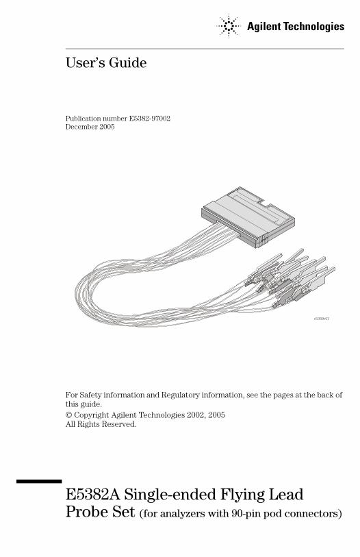
User’s GuidePublication number E5382-97002December 2005
For Safety information and Regulatory information, see the pages at the back of this guide.© Copyright Agilent Technologies 2002, 2005 All Rights Reserved.
E5382A Single-ended Flying Lead Probe Set (for analyzers with 90-pin pod connectors)
In This Book
This guide provides user and service information for the E5382A Single-ended Flying Lead Probe Set.
Chapter 1 gives you general information such as inspection, accessories supplied, and characteristics of the probe.
Chapter 2 shows you how to operate the probe and gives you information about some important aspects of probing and how to get the best results with your probe.
2
Contents
1 General Information
To inspect the probe 7Accessories 8Characteristics and Specifications 9General Characteristics 10To connect and set up the probe set 11
2 Operating the Probe
130 ohm Resistive Signal Pin (orange) and Solder-down Ground Lead 16Input Impedance 17Time domain transmission (TDT) 18Step inputs 21Eye opening 24
5 cm Resistive Signal Lead and Solder-down Ground Lead 27Input Impedance 28Time domain transmission (TDT) 30Step input 33Eye opening 36
Flying Lead and Ground Extender 39Input Impedance 40Time domain transmission (TDT) 41Step input 44Eye opening 47
Grabber Clip and Right-angle Ground Lead 50Input Impedance 51Time domain transmission (TDT) 52Step input 55Eye opening 58
Connecting to coaxial connectors 61Combining grounds 63
3

Contents
4

1
General Information
E5382A Single-ended Flying Lead Probe Set
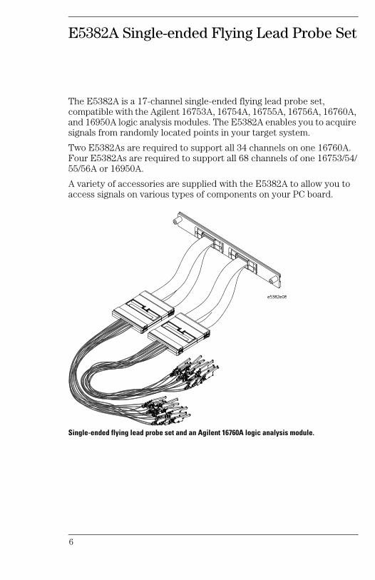
The E5382A is a 17-channel single-ended flying lead probe set, compatible with the Agilent 16753A, 16754A, 16755A, 16756A, 16760A, and 16950A logic analysis modules. The E5382A enables you to acquire signals from randomly located points in your target system.
Two E5382As are required to support all 34 channels on one 16760A. Four E5382As are required to support all 68 channels of one 16753/54/55/56A or 16950A.
A variety of accessories are supplied with the E5382A to allow you to access signals on various types of components on your PC board.
Single-ended flying lead probe set and an Agilent 16760A logic analysis module.
6
General InformationTo inspect the probe
To inspect the probe
Inspect the shipping container for damage.
Keep a damaged shipping container or cushioning material until the contents of the shipment have been checked for completeness and the instrument has been checked mechanically and electrically.
Check the accessories.
Accessories supplied with the instrument are listed in "Accessories Supplied" in table later in this chapter.
• If the contents are incomplete or damaged notify your Agilent Technologies Sales Office.
Inspect the probe.
• If there is mechanical damage or defect, or if the probe does not operate properly or pass performance tests, notify your Agilent Technologies Sales Office.
• If the shipping container is damaged, or the cushioning materials show signs of stress, notify the carrier as well as your Agilent Technologies Sales Office. Keep the shipping materials for the carrier’s inspection. The Agilent Technologies Office will arrange for repair or replacement at Agilent Technologies’ option without waiting for claim settlement.
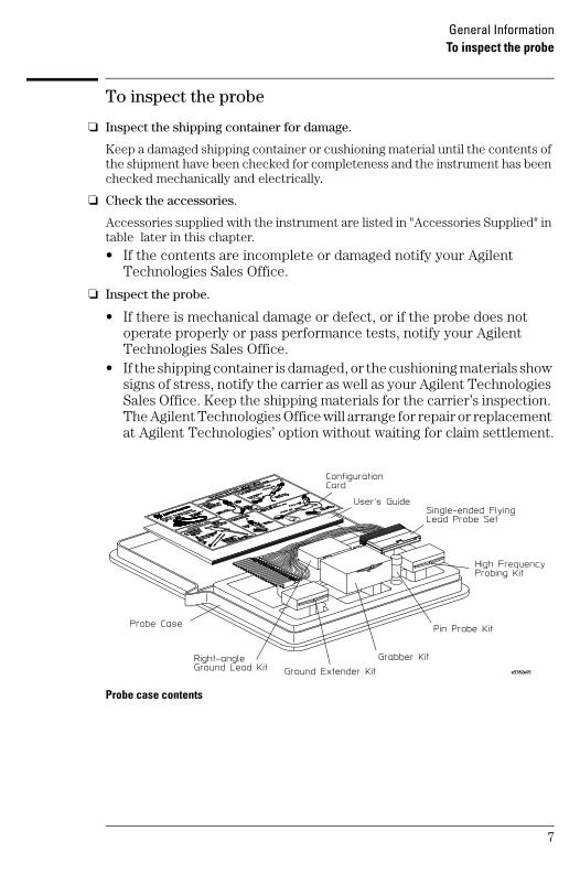
Probe case contents
7

General InformationAccessories
Accessories
The following figure shows the accessories supplied with the E5382A Single-ended Flying Lead Probe Set.
Accessories supplied
The following table shows the part numbers for ordering replacement parts and additional accessories.
Replaceable Parts and Additional Accessories
Description Qty Agilent Part NumberProbe Pin Kit 2 E5382-82102High Frequency Probing Kit (4 resistive signal pins & 4 solder-down grounds)
8 E5382-82101
Ground Extender Kit 20 16517-82105Grabber Clip Kit 20 16517-82109Right-angle Ground Lead Kit 20 16517-82106Cable - Main 1 E5382-61601Probe Tip to BNC Adapter 1 E9638A
8
General InformationCharacteristics and Specifications
Characteristics and Specifications
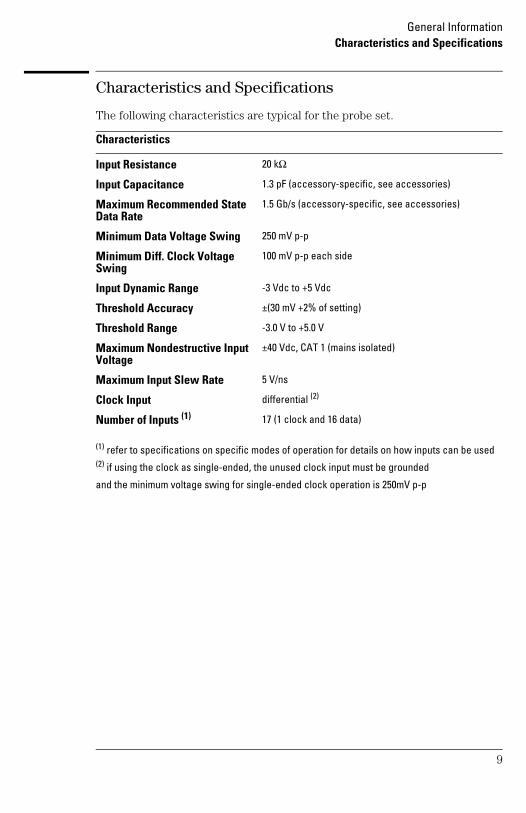
The following characteristics are typical for the probe set.
Characteristics
(1) refer to specifications on specific modes of operation for details on how inputs can be used(2) if using the clock as single-ended, the unused clock input must be grounded
and the minimum voltage swing for single-ended clock operation is 250mV p-p
Input Resistance 20 kΩ
Input Capacitance 1.3 pF (accessory-specific, see accessories)
Maximum Recommended State Data Rate
1.5 Gb/s (accessory-specific, see accessories)
Minimum Data Voltage Swing 250 mV p-p
Minimum Diff. Clock Voltage Swing
100 mV p-p each side
Input Dynamic Range -3 Vdc to +5 Vdc
Threshold Accuracy ±(30 mV +2% of setting)
Threshold Range -3.0 V to +5.0 V
Maximum Nondestructive Input Voltage
±40 Vdc, CAT 1 (mains isolated)
Maximum Input Slew Rate 5 V/ns
Clock Input differential (2)
Number of Inputs (1) 17 (1 clock and 16 data)
9
General InformationGeneral Characteristics
General Characteristics
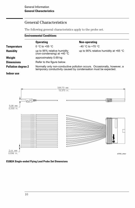
The following general characteristics apply to the probe set.
Environmental Conditions
E5382A Single-ended Flying Lead Probe Set Dimensions
Operating Non-operatingTemperature 0 °C to +55 °C −40 °C to +70 °C
Humidity up to 95% relative humidity (non-condensing) at +40 °C
up to 90% relative humidity at +65 °C
Weight approximately 0.69 kg
Dimensions Refer to the figure below.
Pollution degree 2 Normally only non-conductive pollution occurs. Occasionally, however, a temporary conductivity caused by condensation must be expected.
Indoor use
10
General InformationTo connect and set up the probe set
To connect and set up the probe set
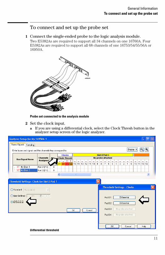
1 Connect the single-ended probe to the logic analysis module. Two E5382As are required to support all 34 channels on one 16760A. Four E5382As are required to support all 68 channels of one 16753/54/55/56A or 16950A.
Probe set connected to the analysis module
2 Set the clock input.a If you are using a differential clock, select the Clock Thresh button in the
analyzer setup screen of the logic analyzer.
Differential threshold
11

General InformationTo connect and set up the probe set
b If your clock is not differential, ground the unused clock input and set the threshold to the desired level.
User defined threshold
3 Connect the flying leads to your target system.The next section in this manual shows the recommended probe configurations in the order of best performance. Select the configuration that works with your target system.
12
2
Operating the Probe
Introduction
The Agilent E5382A single-ended flying lead probe set comes with accessories that trade off flexibility, ease of use, and performance. Discussion and comparisons between four of the most common intended uses of the accessories are included in this section. The table on this page is an overview of the trade-offs between the various accessories. Each of the four configurations have been characterized for probe loading effects, probe step response, and maximum usable state speed. For more detailed information, refer to the pages indicated for each configuration.
When simulating circuits that include a load model for the probe, a simplified model of the probe's input impedance can usually be used. The following table contains information for the simplified model of the probe using suggested accessory configurations. For more accurate load models and detailed discussion of each configuration's performance, refer to the pages indicated.
14

Operating the Probe
Suggested Configurations and Characteristics
Configuration
Description
Total lumped input C
Maximum recommended state speed
Details on page
130 Ω Resistive Signal Pin (orange) and Solder-down Ground Lead
1.3 pF
1.5 Gb/s
page 16
5 cm Resistive Signal Lead and Solder-down Ground Lead
1.6 pF
1.5 Gb/s
page 27
Flying Lead and Ground Extender
1.4 pF
1.5 Gb/s
page 39
Grabber Clip and Right-angle Ground Lead
2.0 pF
600 Mb/s
page 50
15
Operating the Probe130 ohm Resistive Signal Pin (orange) and Solder-down Ground Lead
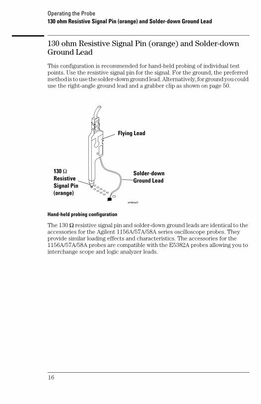
130 ohm Resistive Signal Pin (orange) and Solder-down Ground Lead
This configuration is recommended for hand-held probing of individual test points. Use the resistive signal pin for the signal. For the ground, the preferred method is to use the solder-down ground lead. Alternatively, for ground you could use the right-angle ground lead and a grabber clip as shown on page 50.
Hand-held probing configuration
The 130 Ω resistive signal pin and solder-down ground leads are identical to the accessories for the Agilent 1156A/57A/58A series oscilloscope probes. They provide similar loading effects and characteristics. The accessories for the 1156A/57A/58A probes are compatible with the E5382A probes allowing you to interchange scope and logic analyzer leads.
Flying Lead
Solder-down Ground Lead
130 W Resistive Signal Pin (orange)
16
Operating the Probe130 ohm Resistive Signal Pin (orange) and Solder-down Ground Lead
Input Impedance
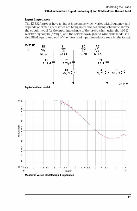
The E5382A probes have an input impedance which varies with frequency, and depends on which accessories are being used. The following schematic shows the circuit model for the input impedance of the probe when using the 130 Ω resistive signal pin (orange) and the solder-down ground wire. This model is a simplified equivalent load of the measured input impedance seen by the target.
Equivalent load model
Measured versus modeled input impedance
2
186
104
4
2
186
4
2
186
4
2
10 1
Mea
sure
d M
odel
104
6 8 1 2 4 6 8 1 2 4 6 8 1
Frequency
2 4 6 8 1 2 4 6 8 1 2 4 6
109
17

Operating the Probe130 ohm Resistive Signal Pin (orange) and Solder-down Ground Lead
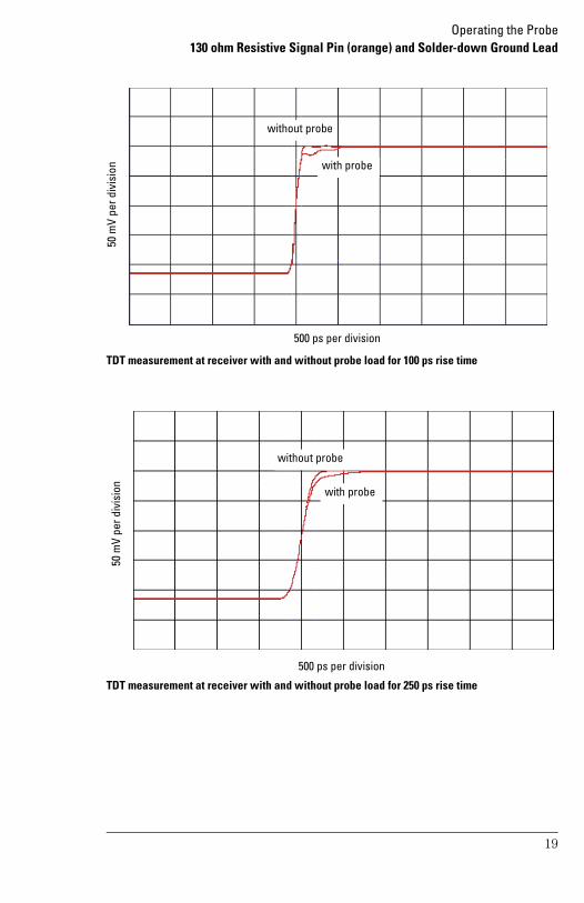
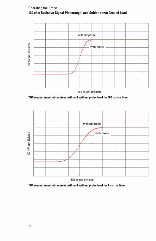
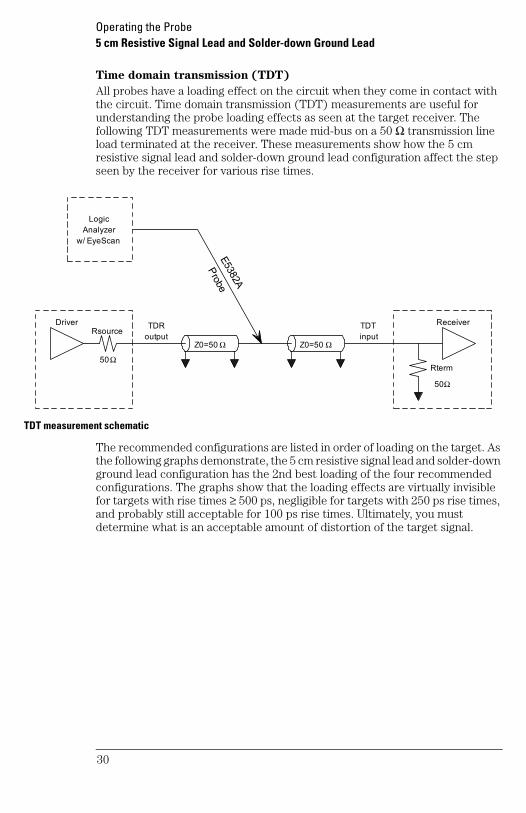
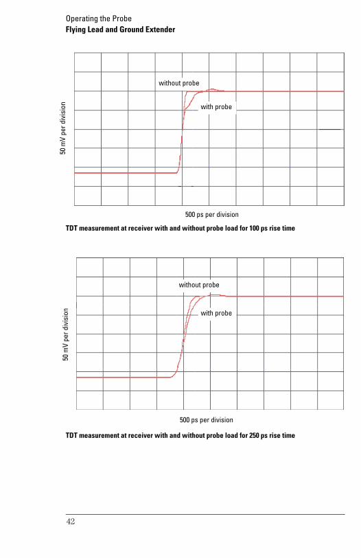
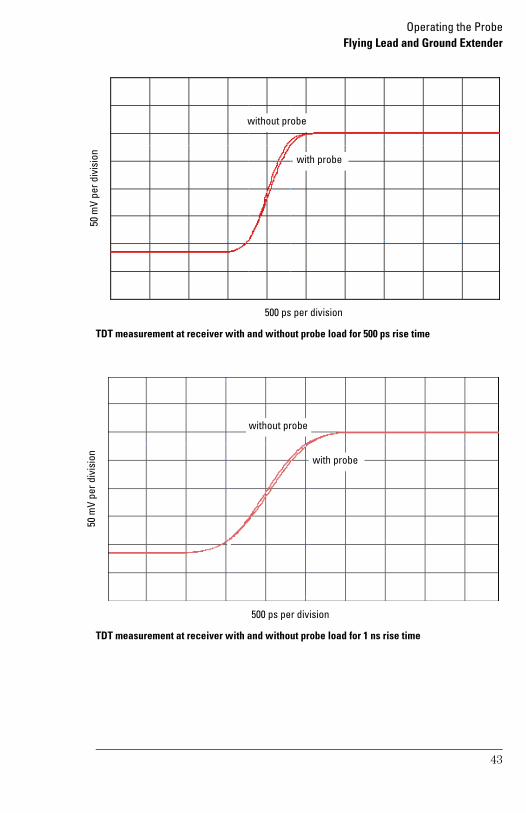
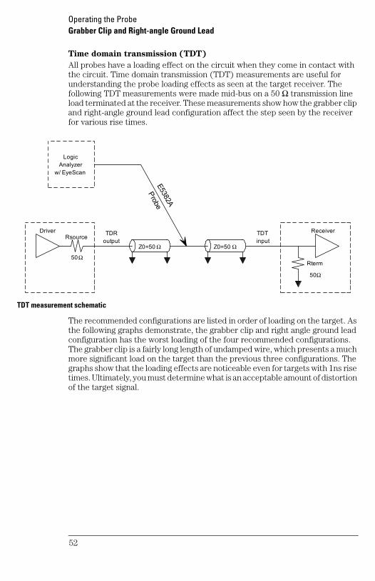
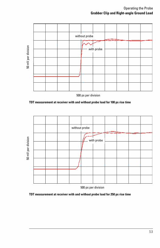
Time domain transmission (TDT)
All probes have a loading effect on the circuit when they come in contact with the circuit. Time domain transmission (TDT) measurements are useful for understanding the probe loading effects as seen at the target receiver. The following TDT measurements were made mid-bus on a 50 Ω transmission line load terminated at the receiver. These measurements show how the 130 Ω resistive signal pin (orange) and solder-down ground lead configuration affect the step seen by the receiver for various rise times.
TDT measurement schematic
As the following graphs demonstrate, the 130 Ω resistive signal pin and solder-down ground lead configuration is the least intrusive of the four recommended configurations. The graphs show that the loading effects are virtually invisible for targets with rise times ≥ 500 ps, negligible for targets with 250 ps rise times, and usable for 100 ps rise times. Ultimately, you must determine what is an acceptable amount of distortion of the target signal.
E5382A
Probe
Z0=50 Ω
Rterm
Driver Receiver Rsource TDR
output
50 Ω
Z0=50 Ω
50 Ω
Logic Analyzer
w/ EyeScan
TDT input
18
Operating the Probe130 ohm Resistive Signal Pin (orange) and Solder-down Ground Lead
TDT measurement at receiver with and without probe load for 100 ps rise time
TDT measurement at receiver with and without probe load for 250 ps rise time
50 m
V pe
r div
isio
n
500 ps per division
without probe
with probe
50 m
V pe
r div
isio
n
500 ps per division
without probe
with probe
19
Operating the Probe130 ohm Resistive Signal Pin (orange) and Solder-down Ground Lead
TDT measurement at receiver with and without probe load for 500 ps rise time
TDT measurement at receiver with and without probe load for 1 ns rise time
50 m
V pe
r div
isio
n
500 ps per division
without probe
with probe
50 m
V pe
r div
isio
n
500 ps per division
without probe
with probe
20
Operating the Probe130 ohm Resistive Signal Pin (orange) and Solder-down Ground Lead
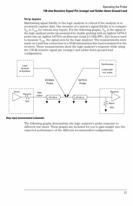
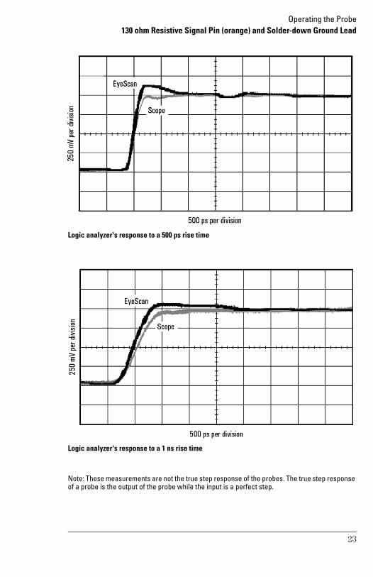
Step inputs
Maintaining signal fidelity to the logic analyzer is critical if the analyzer is to accurately capture data. One measure of a system's signal fidelity is to compare Vin to Vout for various step inputs. For the following graphs, Vin is the signal at the logic analyzer probe tip measured by double probing with an Agilent 54701A probe into an Agilent 54750A oscilloscope (total 2.5 GHz BW). Eye Scan is used to measure Vout, the signal seen by the logic analyzer. The measurements were made on a mid-bus connection to a 50 Ω transmission line load terminated at the receiver. These measurements show the logic analyzer's response while using the 130 Ω resistive signal pin (orange) and solder-down ground lead configuration.
Step input measurement schematic
The following graphs demonstrate the logic analyzer's probe response to different rise times. These graphs are included for you to gain insight into the expected performance of the different recommended configurations.
E5382A Probe
Z0=50 Ω
Rterm
Driver Receiver Rsource Step
output
50 Ω
Z0=50 Ω
50 Ω
Logic Analyzer
w/ EyeScan
Oscilloscope
2.5GHz BW incl. probe
54701A Probe
21

Operating the Probe130 ohm Resistive Signal Pin (orange) and Solder-down Ground Lead
Logic analyzer's response to a 100 ps rise time
Logic analyzer's response to a 250 ps rise time
Note: These measurements are not the true step response of the probes. The true step response of a probe is the output of the probe while the input is a perfect step.
22
Operating the Probe130 ohm Resistive Signal Pin (orange) and Solder-down Ground Lead
Logic analyzer's response to a 500 ps rise time
Logic analyzer's response to a 1 ns rise time
Note: These measurements are not the true step response of the probes. The true step response of a probe is the output of the probe while the input is a perfect step.
23
Operating the Probe130 ohm Resistive Signal Pin (orange) and Solder-down Ground Lead
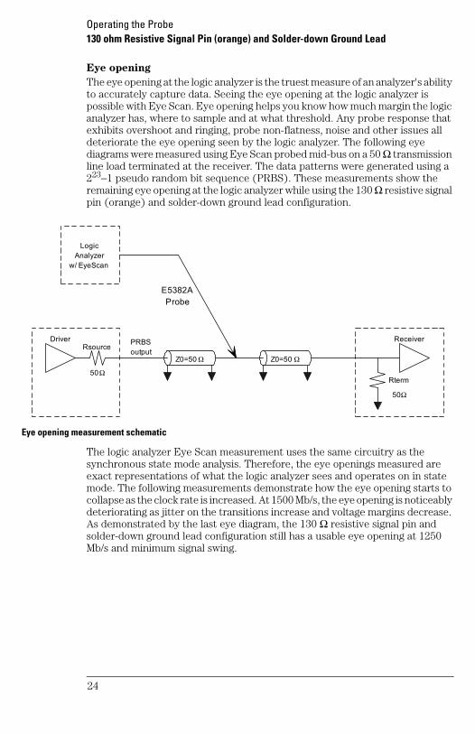
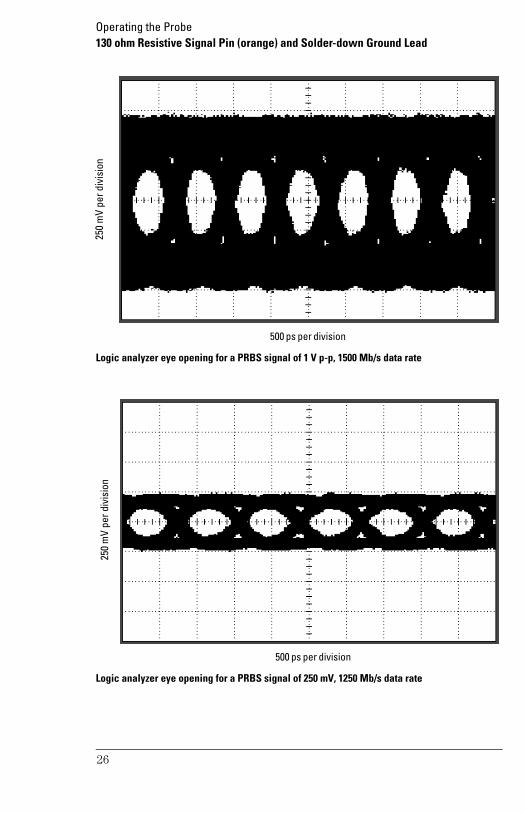
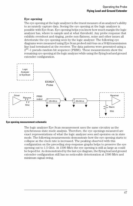
Eye opening
The eye opening at the logic analyzer is the truest measure of an analyzer's ability to accurately capture data. Seeing the eye opening at the logic analyzer is possible with Eye Scan. Eye opening helps you know how much margin the logic analyzer has, where to sample and at what threshold. Any probe response that exhibits overshoot and ringing, probe non-flatness, noise and other issues all deteriorate the eye opening seen by the logic analyzer. The following eye diagrams were measured using Eye Scan probed mid-bus on a 50 Ω transmission line load terminated at the receiver. The data patterns were generated using a 223−1 pseudo random bit sequence (PRBS). These measurements show the remaining eye opening at the logic analyzer while using the 130 Ω resistive signal pin (orange) and solder-down ground lead configuration.
Eye opening measurement schematic
The logic analyzer Eye Scan measurement uses the same circuitry as the synchronous state mode analysis. Therefore, the eye openings measured are exact representations of what the logic analyzer sees and operates on in state mode. The following measurements demonstrate how the eye opening starts to collapse as the clock rate is increased. At 1500 Mb/s, the eye opening is noticeably deteriorating as jitter on the transitions increase and voltage margins decrease. As demonstrated by the last eye diagram, the 130 Ω resistive signal pin and solder-down ground lead configuration still has a usable eye opening at 1250 Mb/s and minimum signal swing.
E5382A Probe
Z0=50 Ω
Rterm
Driver Receiver Rsource
PRBS output
50 Ω
Z0=50 Ω
50 Ω
Logic Analyzer
w/ EyeScan
24

Operating the Probe130 ohm Resistive Signal Pin (orange) and Solder-down Ground Lead
Logic analyzer eye opening for a PRBS signal of 1 V p-p, 1000 Mb/s data rate
Logic analyzer eye opening for a PRBS signal of 1 V p-p, 1250 Mb/s data rate
250
mV
per d
ivis
ion
500 ps per division
250
mV
per d
ivis
ion
500 ps per division
25
Operating the Probe130 ohm Resistive Signal Pin (orange) and Solder-down Ground Lead
Logic analyzer eye opening for a PRBS signal of 1 V p-p, 1500 Mb/s data rate
Logic analyzer eye opening for a PRBS signal of 250 mV, 1250 Mb/s data rate
250
mV
per d
ivis
ion
500 ps per division
250
mV
per d
ivis
ion
500 ps per division
26

Operating the Probe5 cm Resistive Signal Lead and Solder-down Ground Lead
5 cm Resistive Signal Lead and Solder-down Ground Lead
This configuration is recommended for accessing components such as IC leads or surface-mount component leads for hands-off probing.
Surface-mount probe configuration
CAUTION: The resistor bends easily. A bent resistor could affect the performance of the 5 cm resistive signal lead.
The 5cm resistive signal lead and the solder-down ground leads are identical to the accessories for the Agilent 1156A/57A/58A oscilloscope probes. They provide similar loading effects and characteristics. The accessories for the 1156A/57A/58A oscilloscope probes are compatible with the E5382A probes, allowing you to interchange scope and logic analyzer leads.
Flying Lead
5 cm Resistive Signal Pin
Solder-down Ground Lead
27
Operating the Probe5 cm Resistive Signal Lead and Solder-down Ground Lead
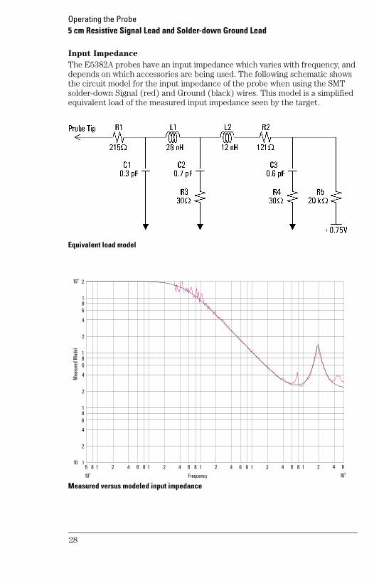
Input Impedance
The E5382A probes have an input impedance which varies with frequency, and depends on which accessories are being used. The following schematic shows the circuit model for the input impedance of the probe when using the SMT solder-down Signal (red) and Ground (black) wires. This model is a simplified equivalent load of the measured input impedance seen by the target.
Equivalent load model
Measured versus modeled input impedance
2
186
104
4
2
186
4
2
186
4
2
Mea
sure
d M
odel
10 1
104
6 8 1 2 4 6 8 1 2 4 6 8 1
Frequency
2 4 6 8 1 2 4 6 8 1 2 4 6
109
28
Operating the Probe5 cm Resistive Signal Lead and Solder-down Ground Lead
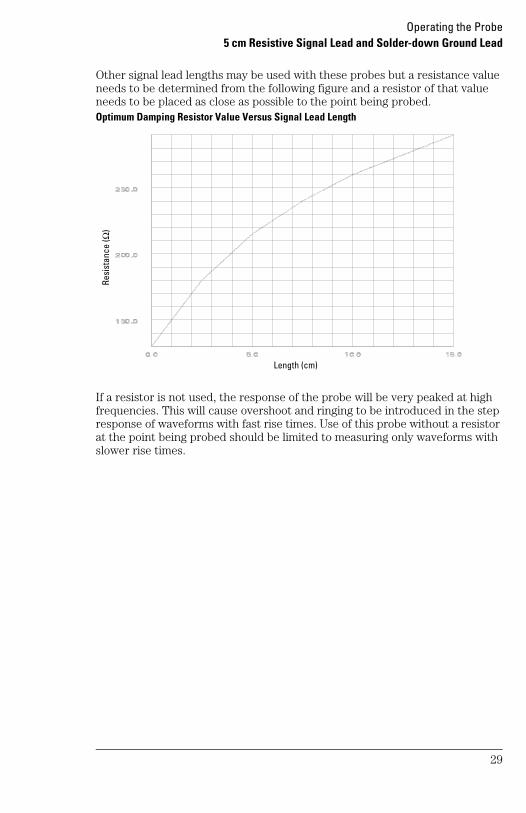
Other signal lead lengths may be used with these probes but a resistance value needs to be determined from the following figure and a resistor of that value needs to be placed as close as possible to the point being probed.Optimum Damping Resistor Value Versus Signal Lead Length
If a resistor is not used, the response of the probe will be very peaked at high frequencies. This will cause overshoot and ringing to be introduced in the step response of waveforms with fast rise times. Use of this probe without a resistor at the point being probed should be limited to measuring only waveforms with slower rise times.
Length (cm)
Resi
stan
ce (Ω
)
29
Operating the Probe5 cm Resistive Signal Lead and Solder-down Ground Lead
Time domain transmission (TDT)
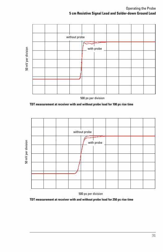
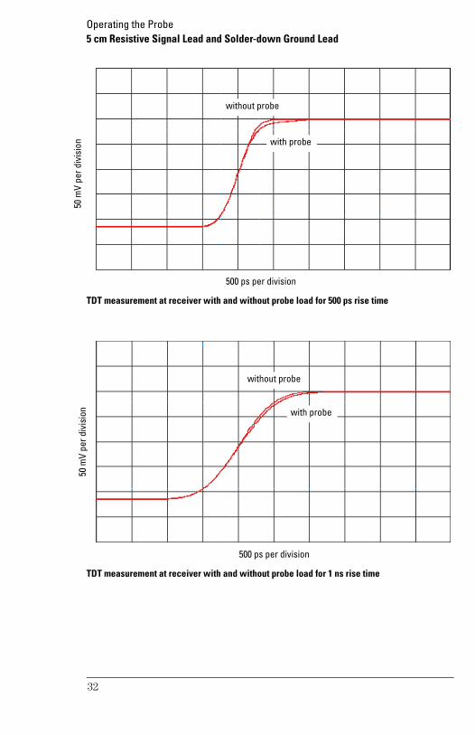
All probes have a loading effect on the circuit when they come in contact with the circuit. Time domain transmission (TDT) measurements are useful for understanding the probe loading effects as seen at the target receiver. The following TDT measurements were made mid-bus on a 50 Ω transmission line load terminated at the receiver. These measurements show how the 5 cm resistive signal lead and solder-down ground lead configuration affect the step seen by the receiver for various rise times.
TDT measurement schematic
The recommended configurations are listed in order of loading on the target. As the following graphs demonstrate, the 5 cm resistive signal lead and solder-down ground lead configuration has the 2nd best loading of the four recommended configurations. The graphs show that the loading effects are virtually invisible for targets with rise times ≥ 500 ps, negligible for targets with 250 ps rise times, and probably still acceptable for 100 ps rise times. Ultimately, you must determine what is an acceptable amount of distortion of the target signal.
E5382A
Probe
Z0=50 Ω
Rterm
Driver Receiver Rsource TDR
output
50 Ω
Z0=50 Ω
50 Ω
Logic Analyzer
w/ EyeScan
TDT input
30
Operating the Probe5 cm Resistive Signal Lead and Solder-down Ground Lead
TDT measurement at receiver with and without probe load for 100 ps rise time
TDT measurement at receiver with and without probe load for 250 ps rise time
50 m
V pe
r div
isio
n
500 ps per division
without probe
with probe
50 m
V pe
r div
isio
n
500 ps per division
without probe
with probe
31
Operating the Probe5 cm Resistive Signal Lead and Solder-down Ground Lead
TDT measurement at receiver with and without probe load for 500 ps rise time
TDT measurement at receiver with and without probe load for 1 ns rise time
50 m
V pe
r div
isio
n
500 ps per division
without probe
with probe
50 m
V pe
r div
isio
n
500 ps per division
without probe
with probe
32
Operating the Probe5 cm Resistive Signal Lead and Solder-down Ground Lead
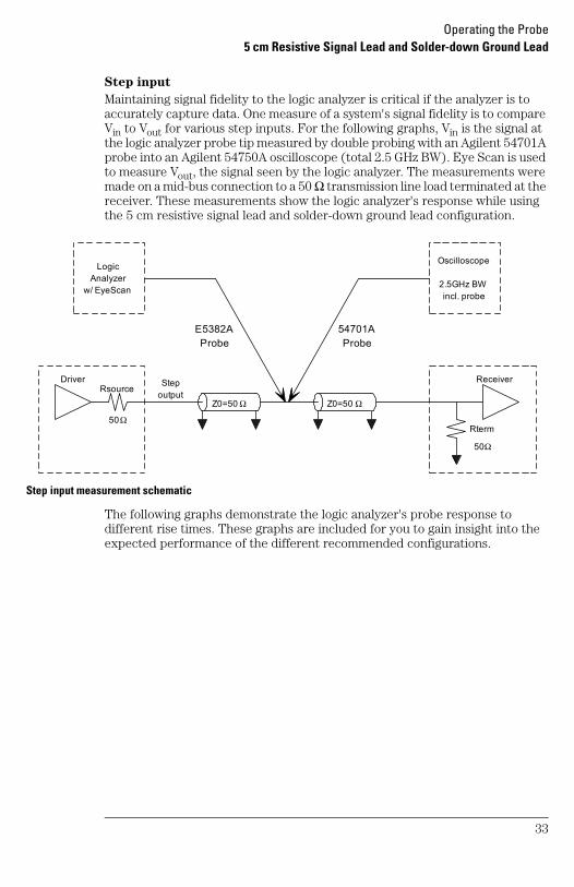
Step input
Maintaining signal fidelity to the logic analyzer is critical if the analyzer is to accurately capture data. One measure of a system's signal fidelity is to compare Vin to Vout for various step inputs. For the following graphs, Vin is the signal at the logic analyzer probe tip measured by double probing with an Agilent 54701A probe into an Agilent 54750A oscilloscope (total 2.5 GHz BW). Eye Scan is used to measure Vout, the signal seen by the logic analyzer. The measurements were made on a mid-bus connection to a 50 Ω transmission line load terminated at the receiver. These measurements show the logic analyzer's response while using the 5 cm resistive signal lead and solder-down ground lead configuration.
Step input measurement schematic
The following graphs demonstrate the logic analyzer's probe response to different rise times. These graphs are included for you to gain insight into the expected performance of the different recommended configurations.
E5382A Probe
Z0=50 Ω
Rterm
Driver Receiver Rsource
Step output
50 Ω
Z0=50 Ω
50 Ω
Logic Analyzer
w/ EyeScan
Oscilloscope
2.5GHz BW incl. probe
54701A Probe
33

Operating the Probe5 cm Resistive Signal Lead and Solder-down Ground Lead
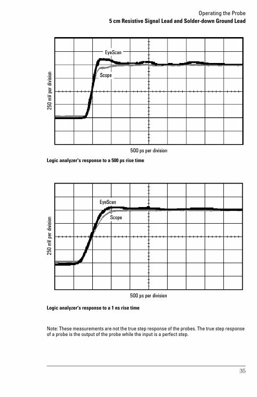
Logic analyzer's response to a 100 ps rise time
Logic analyzer's response to a 250 ps rise time
Note: These measurements are not the true step response of the probes. The true step response of a probe is the output of the probe while the input is a perfect step.
34
Operating the Probe5 cm Resistive Signal Lead and Solder-down Ground Lead
Logic analyzer's response to a 500 ps rise time
Logic analyzer's response to a 1 ns rise time
Note: These measurements are not the true step response of the probes. The true step response of a probe is the output of the probe while the input is a perfect step.
35

Operating the Probe5 cm Resistive Signal Lead and Solder-down Ground Lead
Eye opening
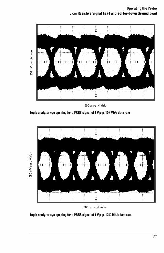
The eye opening at the logic analyzer is the truest measure of an analyzer's ability to accurately capture data. Seeing the eye opening at the logic analyzer is possible with Eye Scan. Eye opening helps you know how much margin the logic analyzer has, where to sample and at what threshold. Any probe response that exhibits overshoot and ringing, probe non-flatness, noise and other issues all deteriorate the eye opening seen by the logic analyzer. The following eye diagrams were measured using Eye Scan probed mid-bus on a 50 Ω transmission line load terminated at the receiver. The data patterns were generated using a 223−1 pseudo random bit sequence (PRBS). These measurements show the remaining eye opening at the logic analyzer while using the 5cm resistive signal lead and solder-down ground lead configuration.
Eye opening measurement schematic
The logic analyzer Eye Scan measurement uses the same circuitry as the synchronous state mode analysis. Therefore, the eye openings measured are exact representations of what the logic analyzer sees and operates on in state mode. The following measurements demonstrate how the eye opening starts to collapse as the clock rate is increased. At 1500 Mb/s, the eye opening is noticeably deteriorating as jitter on the transitions increase and voltage margins decrease. The bandwidth limiting of the 5 cm resistive signal lead causes more roll-off on the transitions. As demonstrated by the last eye diagram, the 5 cm resistive signal lead and solder-down ground lead configuration still has a usable eye opening at 1250Mb/s and minimum signal swing.
E5382A Probe
Z0=50 Ω
Rterm
Driver Receiver Rsource PRBS
output
50 Ω
Z0=50 Ω
50 Ω
Logic Analyzer
w/ EyeScan
36
Operating the Probe5 cm Resistive Signal Lead and Solder-down Ground Lead
Logic analyzer eye opening for a PRBS signal of 1 V p-p, 100 Mb/s data rate
Logic analyzer eye opening for a PRBS signal of 1 V p-p, 1250 Mb/s data rate
250
mV
per d
ivis
ion
500 ps per division
250
mV
per d
ivis
ion
500 ps per division
37

Operating the Probe5 cm Resistive Signal Lead and Solder-down Ground Lead
Logic analyzer eye opening for a PRBS signal of 1 V p-p, 1500 Mb/s data rate
Logic analyzer eye opening for a PRBS signal of 250 mV p-p, 1250 Mb/s data rate
250
mV
per d
ivis
ion
500 ps per division
250
mV
per d
ivis
ion
500 ps per division
38
Operating the ProbeFlying Lead and Ground Extender
Flying Lead and Ground Extender
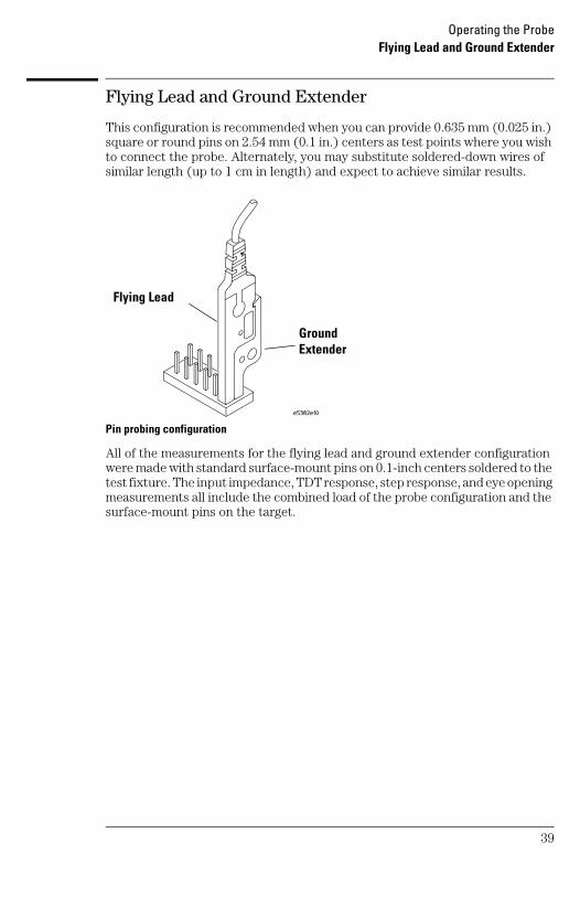
This configuration is recommended when you can provide 0.635 mm (0.025 in.) square or round pins on 2.54 mm (0.1 in.) centers as test points where you wish to connect the probe. Alternately, you may substitute soldered-down wires of similar length (up to 1 cm in length) and expect to achieve similar results.
Pin probing configuration
All of the measurements for the flying lead and ground extender configuration were made with standard surface-mount pins on 0.1-inch centers soldered to the test fixture. The input impedance, TDT response, step response, and eye opening measurements all include the combined load of the probe configuration and the surface-mount pins on the target.
Flying Lead
Ground Extender
39

Operating the ProbeFlying Lead and Ground Extender
Input Impedance
The E5382A probes have an input impedance which varies with frequency, and depends on which accessories are being used. The following schematic shows the circuit model for the input impedance of the probe when using the ground extender clip. This model is a simplified equivalent load of the measured input impedance seen by the target.
Equivalent load model
Measured versus modeled input impedance
2
186
104
4
2
186
4
2
186
4
2
10 1
Mea
sure
d M
odel
104
6 8 1 2 4 6 8 1 2 4 6 8 1
Frequency
2 4 6 8 1 2 4 6 8 1 2 4 6
109
40
Operating the ProbeFlying Lead and Ground Extender
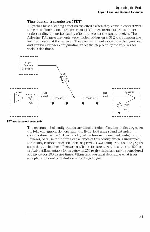
Time domain transmission (TDT)
All probes have a loading effect on the circuit when they come in contact with the circuit. Time domain transmission (TDT) measurements are useful for understanding the probe loading effects as seen at the target receiver. The following TDT measurements were made mid-bus on a 50 Ω transmission line load terminated at the receiver. These measurements show how the flying lead and ground extender configuration affect the step seen by the receiver for various rise times.
TDT measurement schematic
The recommended configurations are listed in order of loading on the target. As the following graphs demonstrate, the flying lead and ground extender configuration has the 3rd best loading of the four recommended configurations. However, because most of the capacitance of this configuration is undamped, the loading is more noticeable than the previous two configurations. The graphs show that the loading effects are negligible for targets with rise times ≥ 500 ps, probably still acceptable for targets with 250 ps rise times, and may be considered significant for 100 ps rise times. Ultimately, you must determine what is an acceptable amount of distortion of the target signal.
E5382A
Probe
Z0=50 Ω
Rterm
Driver Receiver Rsource TDR
output
50 Ω
Z0=50 Ω
50 Ω
Logic Analyzer
w/ EyeScan
TDT input
41
Operating the ProbeFlying Lead and Ground Extender
TDT measurement at receiver with and without probe load for 100 ps rise time
TDT measurement at receiver with and without probe load for 250 ps rise time
50 m
V pe
r div
isio
n
500 ps per division
without probe
with probe
50 m
V pe
r div
isio
n
500 ps per division
without probe
with probe
42
Operating the ProbeFlying Lead and Ground Extender
TDT measurement at receiver with and without probe load for 500 ps rise time
TDT measurement at receiver with and without probe load for 1 ns rise time
50 m
V pe
r div
isio
n
500 ps per division
without probe
with probe
50 m
V pe
r div
isio
n
500 ps per division
without probe
with probe
43

Operating the ProbeFlying Lead and Ground Extender
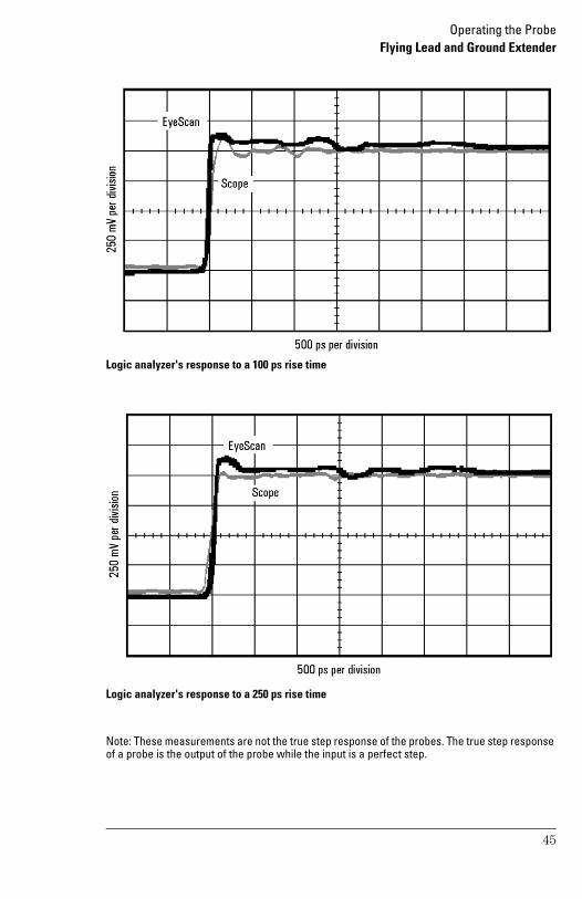
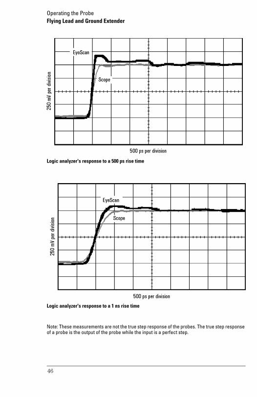
Step input
Maintaining signal fidelity to the logic analyzer is critical if the analyzer is to accurately capture data. One measure of a system's signal fidelity is to compare Vin to Vout for various step inputs. For the following graphs, Vin is the signal at the logic analyzer probe tip measured by double probing with an Agilent 54701A probe into an Agilent 54750A oscilloscope (total 2.5 GHz BW). Eye Scan is used to measure Vout, the signal seen by the logic analyzer. The measurements were made on a mid-bus connection to a 50 Ω transmission line load terminated at the receiver. These measurements show the logic analyzer's response while using the flying lead and ground extender configuration.
Step measurement schematic
The following graphs demonstrate the logic analyzer's probe response to different rise times. These graphs are included for you to gain insight into the expected performance of the different recommended accessory configurations.
E5382A Probe
Z0=50 Ω
Rterm
Driver Receiver Rsource Step
output
50 Ω
Z0=50 Ω
50 Ω
Logic Analyzer
w/ EyeScan
Oscilloscope
2.5GHz BW incl. probe
54701A Probe
44
Operating the ProbeFlying Lead and Ground Extender
Logic analyzer's response to a 100 ps rise time
Logic analyzer's response to a 250 ps rise time
Note: These measurements are not the true step response of the probes. The true step response of a probe is the output of the probe while the input is a perfect step.
45
Operating the ProbeFlying Lead and Ground Extender
Logic analyzer's response to a 500 ps rise time
Logic analyzer's response to a 1 ns rise time
Note: These measurements are not the true step response of the probes. The true step response of a probe is the output of the probe while the input is a perfect step.
46
Operating the ProbeFlying Lead and Ground Extender
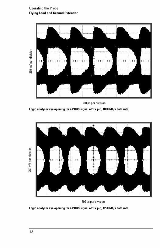
Eye opening
The eye opening at the logic analyzer is the truest measure of an analyzer's ability to accurately capture data. Seeing the eye opening at the logic analyzer is possible with Eye Scan. Eye opening helps you know how much margin the logic analyzer has, where to sample and at what threshold. Any probe response that exhibits overshoot and ringing, probe non-flatness, noise and other issues all deteriorate the eye opening seen by the logic analyzer. The following eye diagrams were measured using Eye Scan probed mid-bus on a 50 Ω transmission line load terminated at the receiver. The data patterns were generated using a 223−1 pseudo random bit sequence (PRBS). These measurements show the remaining eye opening at the logic analyzer while using the flying lead and ground extender configuration.
Eye opening measurement schematic
The logic analyzer Eye Scan measurement uses the same circuitry as the synchronous state mode analysis. Therefore, the eye openings measured are exact representations of what the logic analyzer sees and operates on in state mode. The following measurements demonstrate how the eye opening starts to collapse as the clock rate is increased. The peaking observed with this configuration on the preceding step-response graphs helps to preserve the eye opening out to 1.5 Gb/s. At 1500 Mb/s the eye opening is still as large as could be hoped for. As demonstrated by the last eye diagram, the flying lead and ground extender configuration still has no noticeable deterioration at 1500 Mb/s and minimum signal swing.
E5382A Probe
Z0=50 Ω
Rterm
Driver Receiver Rsource PRBS
output
50 Ω
Z0=50 Ω
50 Ω
Logic Analyzer
w/ EyeScan
47
Operating the ProbeFlying Lead and Ground Extender
Logic analyzer eye opening for a PRBS signal of 1 V p-p, 1000 Mb/s data rate
Logic analyzer eye opening for a PRBS signal of 1 V p-p, 1250 Mb/s data rate
250
mV
per d
ivis
ion
500 ps per division
250
mV
per d
ivis
ion
500 ps per division
48

Operating the ProbeFlying Lead and Ground Extender
Logic analyzer eye opening for a PRBS signal of 1 V p-p, 1500 Mb/s data rate
Logic analyzer eye opening for a PRBS signal of 250 mV p-p, 1500 Mb/s data rate
250
mV
per d
ivis
ion
500 ps per division
250
mV
per d
ivis
ion
500 ps per division
49
Operating the ProbeGrabber Clip and Right-angle Ground Lead
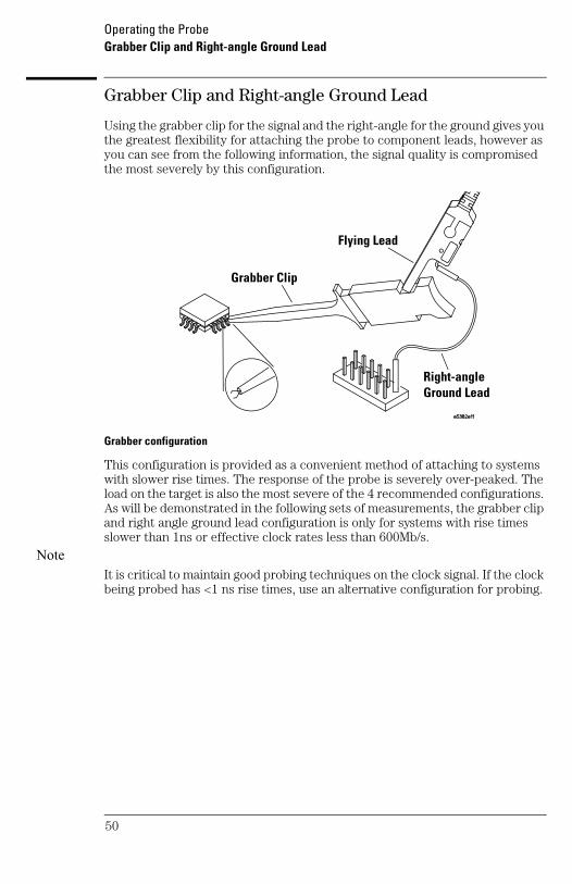
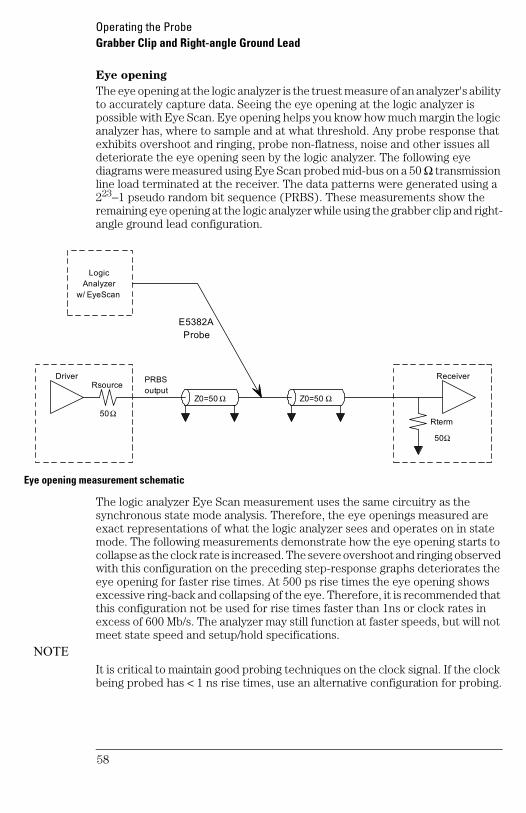
Grabber Clip and Right-angle Ground Lead
Using the grabber clip for the signal and the right-angle for the ground gives you the greatest flexibility for attaching the probe to component leads, however as you can see from the following information, the signal quality is compromised the most severely by this configuration.
Grabber configuration
This configuration is provided as a convenient method of attaching to systems with slower rise times. The response of the probe is severely over-peaked. The load on the target is also the most severe of the 4 recommended configurations. As will be demonstrated in the following sets of measurements, the grabber clip and right angle ground lead configuration is only for systems with rise times slower than 1ns or effective clock rates less than 600Mb/s.
NoteIt is critical to maintain good probing techniques on the clock signal. If the clock being probed has <1 ns rise times, use an alternative configuration for probing.
Grabber Clip
Flying Lead
Right-angle Ground Lead
50
Operating the ProbeGrabber Clip and Right-angle Ground Lead
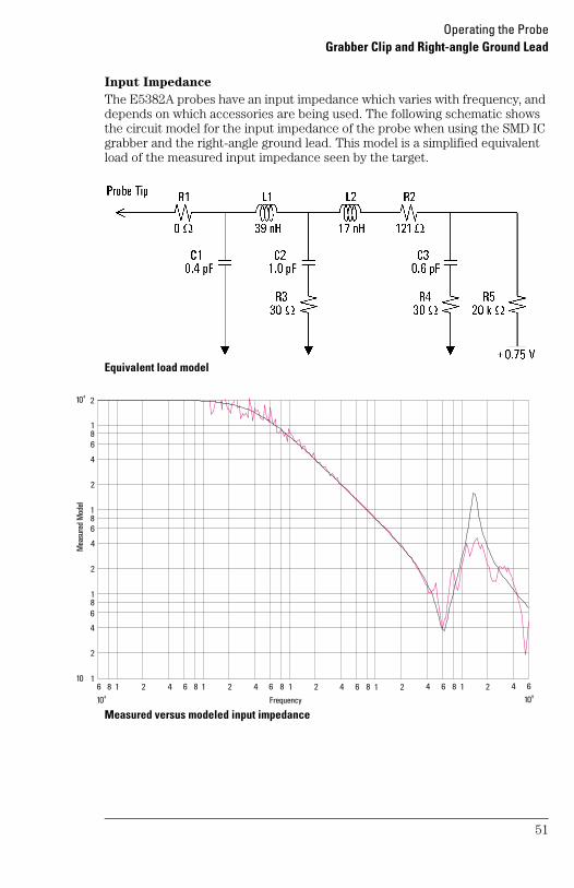
Input Impedance
The E5382A probes have an input impedance which varies with frequency, and depends on which accessories are being used. The following schematic shows the circuit model for the input impedance of the probe when using the SMD IC grabber and the right-angle ground lead. This model is a simplified equivalent load of the measured input impedance seen by the target.
Equivalent load model
Measured versus modeled input impedance
2
186
104
4
2
186
4
2
186
4
2
10 1
Mea
sure
d M
odel
104
6 8 1 2 4 6 8 1 2 4 6 8 1
Frequency
2 4 6 8 1 2 4 6 8 1 2 4 6
109
51
Operating the ProbeGrabber Clip and Right-angle Ground Lead
Time domain transmission (TDT)
All probes have a loading effect on the circuit when they come in contact with the circuit. Time domain transmission (TDT) measurements are useful for understanding the probe loading effects as seen at the target receiver. The following TDT measurements were made mid-bus on a 50 Ω transmission line load terminated at the receiver. These measurements show how the grabber clip and right-angle ground lead configuration affect the step seen by the receiver for various rise times.
TDT measurement schematic
The recommended configurations are listed in order of loading on the target. As the following graphs demonstrate, the grabber clip and right angle ground lead configuration has the worst loading of the four recommended configurations. The grabber clip is a fairly long length of undamped wire, which presents a much more significant load on the target than the previous three configurations. The graphs show that the loading effects are noticeable even for targets with 1ns rise times. Ultimately, you must determine what is an acceptable amount of distortion of the target signal.
E5382A
Probe
Z0=50 Ω
Rterm
Driver Receiver Rsource TDR
output
50 Ω
Z0=50 Ω
50 Ω
Logic Analyzer
w/ EyeScan
TDT input
52
Operating the ProbeGrabber Clip and Right-angle Ground Lead
TDT measurement at receiver with and without probe load for 100 ps rise time
TDT measurement at receiver with and without probe load for 250 ps rise time
50 m
V pe
r div
isio
n
500 ps per division
without probe
with probe
50 m
V pe
r div
isio
n
500 ps per division
without probe
with probe
53

Operating the ProbeGrabber Clip and Right-angle Ground Lead
TDT measurement at receiver with and without probe load for 500 ps rise time
TDT measurement at receiver with and without probe load for 1 ns rise time
50 m
V pe
r div
isio
n
500 ps per division
without probe
with probe
50 m
V pe
r div
isio
n
500 ps per division
without probe
with probe
54

Operating the ProbeGrabber Clip and Right-angle Ground Lead
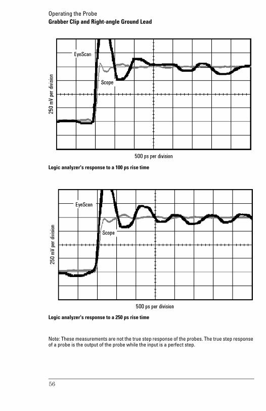
Step input
Maintaining signal fidelity to the logic analyzer is critical if the analyzer is to accurately capture data. One measure of a system's signal fidelity is to compare Vin to Vout for various step inputs. For the following graphs, Vin is the signal at the logic analyzer probe tip measured by double probing with an Agilent 54701A probe into an Agilent 54750A oscilloscope (total 2.5 GHz BW). Eye Scan is used to measure Vout, the signal seen by the logic analyzer. The measurements were made on a mid-bus connection to a 50 Ω transmission line load terminated at the receiver. These measurements show the logic analyzer's response while using the grabber clip and right-angle ground lead configuration.
Step measurement schematic
The following graphs demonstrate the logic analyzer's probe response to different rise times. These graphs are included for you to gain insight into the expected performance of the different recommended accessory configurations, particularly for the grabber clip and right-angle ground lead configuration. As the following graphs will demonstrate, the use of the undamped grabber clip results in excessive overshoot and ringing at the logic analyzer for targets with < 1 ns rise times.
E5382A Probe
Z0=50 Ω
Rterm
Driver Receiver Rsource Step
output
50 Ω
Z0=50 Ω
50 Ω
Logic Analyzer
w/ EyeScan
Oscilloscope
2.5GHz BW incl. probe
54701A Probe
55
Operating the ProbeGrabber Clip and Right-angle Ground Lead
Logic analyzer's response to a 100 ps rise time
Logic analyzer's response to a 250 ps rise time
Note: These measurements are not the true step response of the probes. The true step response of a probe is the output of the probe while the input is a perfect step.
56

Operating the ProbeGrabber Clip and Right-angle Ground Lead
Logic analyzer's response to a 500 ps rise time
Logic analyzer's response to a 1 ns rise time
Note: These measurements are not the true step response of the probes. The true step response of a probe is the output of the probe while the input is a perfect step.
57
Operating the ProbeGrabber Clip and Right-angle Ground Lead
Eye opening
The eye opening at the logic analyzer is the truest measure of an analyzer's ability to accurately capture data. Seeing the eye opening at the logic analyzer is possible with Eye Scan. Eye opening helps you know how much margin the logic analyzer has, where to sample and at what threshold. Any probe response that exhibits overshoot and ringing, probe non-flatness, noise and other issues all deteriorate the eye opening seen by the logic analyzer. The following eye diagrams were measured using Eye Scan probed mid-bus on a 50 Ω transmission line load terminated at the receiver. The data patterns were generated using a 223−1 pseudo random bit sequence (PRBS). These measurements show the remaining eye opening at the logic analyzer while using the grabber clip and right-angle ground lead configuration.
Eye opening measurement schematic
The logic analyzer Eye Scan measurement uses the same circuitry as the synchronous state mode analysis. Therefore, the eye openings measured are exact representations of what the logic analyzer sees and operates on in state mode. The following measurements demonstrate how the eye opening starts to collapse as the clock rate is increased. The severe overshoot and ringing observed with this configuration on the preceding step-response graphs deteriorates the eye opening for faster rise times. At 500 ps rise times the eye opening shows excessive ring-back and collapsing of the eye. Therefore, it is recommended that this configuration not be used for rise times faster than 1ns or clock rates in excess of 600 Mb/s. The analyzer may still function at faster speeds, but will not meet state speed and setup/hold specifications.
NOTEIt is critical to maintain good probing techniques on the clock signal. If the clock being probed has < 1 ns rise times, use an alternative configuration for probing.
E5382A Probe
Z0=50 Ω
Rterm
Driver Receiver Rsource PRBS
output
50 Ω
Z0=50 Ω
50 Ω
Logic Analyzer
w/ EyeScan
58
Operating the ProbeGrabber Clip and Right-angle Ground Lead
Logic analyzer eye opening for a PRBS signal of 1 V p-p, 500 Mb/s data rate, 1 ns rise time
Logic analyzer eye opening for a PRBS signal of 1 V p-p, 500 Mb/s data rate, 500 ps rise time
250
mV
per d
ivis
ion
500 ps per division
250
mV
per d
ivis
ion
500 ps per division
59
Operating the ProbeGrabber Clip and Right-angle Ground Lead
Logic analyzer eye opening for a PRBS signal of 1 V p-p, 600 Mb/s data rate, 1 ns rise time
Logic analyzer eye opening for a PRBS signal of 250 mV, 600 Mb/s data rate, 1 ns rise time
250
mV
per d
ivis
ion
500 ps per division
250
mV
per d
ivis
ion
500 ps per division
60

Operating the ProbeConnecting to coaxial connectors
Connecting to coaxial connectors
You can use the Agilent E9638A to adapt the probe tip to a BNC connector. The adapter and the BNC connector itself will add significant capacitance to the probe load. You can generally assume (though not always) that a BNC connector is intended to form a part of a transmission line terminated in 50 Ω (the characteristic impedance of BNC connectors is 50 Ω). So, the best solution for maintaining signal integrity is to terminate the line in 50 Ω after the BNC connector and a close as possible to the probe tip. That technique minimizes the length of the unterminated stub past the termination. The following picture shows the recommended configuration to achieve this.
NoteThis configuration has not been characterized for target loading or logic analyzer performance. Therefore no recommendations are being made or implied as to the expected performance of this configuration.
BNC connector
BNC 50 FeedthroughTermination Adapter
Ω
Probe Tip
BNC Connector
E9638A Probe Tipto BNC Adapter
61
Operating the ProbeConnecting to coaxial connectors
SMA, SMB, SMC, or other coaxial connectors
BNC 50 FeedthroughTermination Adapter
Ω
Probe Tip
E9638A Probe Tipto BNC Adapter
BNC to SMA, SMB, SMCor other Coaxial Adapter
SMA, SMB, SMCor other Coaxial Connector
62
Operating the ProbeCombining grounds
Combining grounds
It is essential to ground every tip that is in use. For best performance at high speeds, every tip should be grounded individually to ground in the system under test. For convenience in connecting grounds, you can use the ground connector, Agilent part number 16515-27601, to combine four probe tip grounds to connect to one ground point in the system under test.Using the 16515-27601 to combine grounds will have some negative impact on performance due to coupling caused by common ground return currents. The exact impact depends on the signals being tested and the configuration of the test, so it is impossible to predict accurately. In general, the faster the rise time of the signals under test, the greater the risk of coupling. In no case should more than four tip grounds be combined through one 16515-27601 to connect to ground in the system under test.
63

Operating the ProbeCombining grounds
64
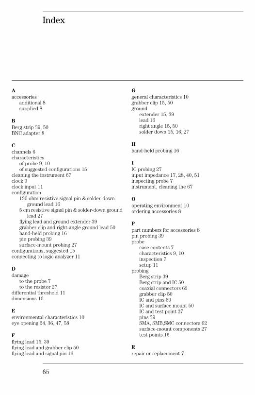
Index
A
accessoriesadditional 8supplied 8
B
Berg strip 39, 50BNC adapter 8
C
channels 6characteristics
of probe 9, 10of suggested configurations 15
cleaning the instrument 67clock 9clock input 11configuration
130 ohm resistive signal pin & solder-down ground lead 16
5 cm resistive signal pin & solder-down ground lead 27
flying lead and ground extender 39grabber clip and right-angle ground lead 50hand-held probing 16pin probing 39surface-mount probing 27
configurations, suggested 15connecting to logic analyzer 11
D
damageto the probe 7to the resistor 27
differential threshold 11dimensions 10
E
environmental characteristics 10eye opening 24, 36, 47, 58
F
flying lead 15, 39flying lead and grabber clip 50flying lead and signal pin 16
G
general characteristics 10grabber clip 15, 50ground
extender 15, 39lead 16right angle 15, 50solder down 15, 16, 27
H
hand-held probing 16
I
IC probing 27input impedance 17, 28, 40, 51inspecting probe 7instrument, cleaning the 67
O
operating environment 10ordering accessories 8
P
part numbers for accessories 8pin probing 39probe
case contents 7characteristics 9, 10inspection 7setup 11
probingBerg strip 39Berg strip and IC 50coaxial connectors 62grabber clip 50IC and pins 50IC and surface mount 50IC and test point 27pins 39SMA, SMB,SMC connectors 62surface-mount components 27test points 16
R
repair or replacement 7
65
replaceable parts 8resistive signal
lead, 5 cm 15, 27pin, 130 ohm 15, 16
S
setting up the probe & logic analyzer 11SMA,SMB,SMC connectors 62solder-down ground 16, 27specifications 9state data rate 9step input 21, 33, 44, 55suggested configurations 15surface-mount probing 27
T
TDT 18, 30, 41, 52test point 16, 27threshold
accuracy 9differential 11range 9user defined 12
U
user defined threshold 12
W
weight 10
66
Safety NoticesThis apparatus has been designed and tested in accordance with IEC Pub-lication 1010, Safety Requirements for Measur-ing Apparatus, and has been supplied in a safe condition. This is a Safety Class I instrument (pro-vided with terminal for protective earthing). Before applying power, verify that the correct safety precautions are taken (see the following warnings). In addition, note the external mark-ings on the instrument that are described under "Safety Symbols."
Warnings• Before turning on the instrument, you must con-nect the protective earth terminal of the instrument to the protective conduc-tor of the (mains) power cord. The mains plug shall only be inserted in a socket outlet provided with a protective earth contact. You must not negate the protective action by using an exten-sion cord (power cable) without a protective con-ductor (grounding). Grounding one conductor of a two-conductor outlet is not sufficient protection.
• Only fuses with the required rated current, voltage, and specified type (normal blow, time delay, etc.) should be used. Do not use repaired fuses or short-circuited fuseholders. To do so could cause a shock or fire hazard.
• If you energize this instrument by an auto transformer (for voltage reduction or mains isola-tion), the common termi-nal must be connected to the earth terminal of the power source.
• Whenever it is likely that the ground protection is impaired, you must make the instrument inopera-tive and secure it against any unintended operation.
• Service instructions are for trained service person-nel. To avoid dangerous electric shock, do not per-form any service unless qualified to do so. Do not attempt internal service or adjustment unless another person, capable of render-ing first aid and resuscita-tion, is present.
• Do not install substitute parts or perform any unauthorized modification to the instrument.
• Capacitors inside the instrument may retain a charge even if the instru-ment is disconnected from its source of supply.
• Do not operate the instrument in the pres-ence of flammable gasses or fumes. Operation of any electrical instrument in such an environment constitutes a definite safety hazard.
• Do not use the instru-ment in a manner not specified by the manufac-turer.
To clean the instrumentIf the instrument requires cleaning: (1) Remove power from the instru-ment. (2) Clean the exter-nal surfaces of the instrument with a soft
cloth dampened with a mixture of mild detergent and water. (3) Make sure that the instrument is completely dry before reconnecting it to a power source.
Safety Symbols
Instruction manual sym-bol: the product is marked with this symbol when it is necessary for you to refer to the instruction manual in order to protect against damage to the product..
Hazardous voltage sym-bol.
Earth terminal symbol: Used to indicate a circuit common connected to grounded chassis.
!
Agilent Technologies P.O. Box 2197 1900 Garden of the Gods Road Colorado Springs, CO 80901
Notices© Agilent Technologies, Inc. 2002, 2005No part of this manual may be reproduced in any form or by any means (including electronic stor-age and retrieval or trans-lation into a foreign language) without prior agreement and written consent from Agilent Technologies, Inc. as gov-erned by United States and international copy-right laws.
Manual Part NumberE5382-97002, December 2005
Print HistoryE5382-97000, April 2002 E5382-97001, Sept. 2002 E5382-97002, Dec. 2005
Agilent Technologies, Inc. 1900 Garden of the Gods Road Colorado Springs, CO 80907 USA
Restricted Rights LegendIf software is for use in the performance of a U.S. Government prime con-tract or subcontract, Soft-ware is delivered and licensed as “Commercial computer software” as defined in DFAR 252.227-7014 (June 1995), or as a “commercial item” as defined in FAR 2.101(a) or as “Restricted computer software” as defined in FAR 52.227-19 (June 1987) or any equivalent agency regulation or contract clause. Use, duplication or disclosure of Software is subject to Agilent Tech-nologies’ standard com-mercial license terms, and non-DOD Departments and Agencies of the U.S. Government will receive no greater than Restricted Rights as defined in FAR
52.227-19(c)(1-2) (June 1987). U.S. Government users will receive no greater than Limited Rights as defined in FAR 52.227-14 (June 1987) or DFAR 252.227-7015 (b)(2) (November 1995), as appli-cable in any technical data.
Document WarrantyThe material con-tained in this docu-ment is provided “as is,” and is subject to being changed, with-out notice, in future editions. Further, to the maximum extent per-mitted by applicable law, Agilent disclaims all warranties, either express or implied, with regard to this manual and any infor-mation contained herein, including but not limited to the implied warranties of merchantability and fit-ness for a particular purpose. Agilent shall not be liable for errors or for incidental or consequential dam-ages in connection with the furnishing, use, or performance of this document or of any information contained herein. Should Agilent and the user have a separate written agreement with war-ranty terms covering the material in this document that conflict with these terms, the warranty terms in the separate agreement shall control.
Technology Licenses The hardware and/or soft-ware described in this
document are furnished under a license and may be used or copied only in accordance with the terms of such license.
WARNING
A WARNING notice denotes a hazard. It calls attention to an operating procedure, practice, or the like that, if not correctly performed or adhered to, could result in personal injury or death. Do not proceed beyond a WARNING notice until the indicated conditions are fully understood and met.
CAUTION
A CAUTION notice denotes a hazard. It calls attention to an operating procedure, practice, or the like that, if not correctly performed or adhered to, could result in damage to the product or loss of important data. Do not proceed beyond a CAUTION notice until the indicated conditions are fully understood and met.
Trademark Acknowledgements
Agilent Technologies Printed in the USAManual Part Number E5382-97002
*E5382-97001*