Embed Size (px)
Citation preview

FN6944Rev 2.00
April 14, 2015
ISL58214Programmable High Speed Single Channel Laser Diode Driver
DATASHEETNOT RECOMMENDED FOR NEW DESIGNS
NO RECOMMENDED REPLACEMENT
contact our Technical Support Center at
1-888-INTERSIL or www.intersil.com/tsc
The ISL58214 is a highly integrated laser diode driver designed to support a laser beam scanning MEMS projector. Operating from a single 5V analog supply, it directly drives either a cathode-grounded laser, or a floating laser whose anode is connected to a high voltage supply. The ISL58214 is configured through a serial interface.
An integrated 10-bit high power DAC drives the selected laser. The desired current level can be scaled by a 10-bit DAC programmed through a serial interface or the ISLOPE pin to compensate for ambient brightness, speed variation or laser sensitivity change.
The CLK pin clocks in the data on the rising edge of CLK. The LOWP line gates the output off when HIGH.
Features• Direct drive for floating laser, or cathode grounded. Supports
Red, ‘Green’ or Blue laser
• Up to 1000mA maximum total output (ISRC) with 1.5ns typical tr/tf
• Up to 500mA maximum total output (ISNK) with 1ns typical tr/tf.
• 10-bit x 10-bit multiplying DAC output provides 10-bit full scale adjustment and 10-bit resolution at any full scale output
• ISLOPE input allows compensation for laser slope, ambient light, and sweep speed variation
• High-speed SPI Serial input works up to 50MHz
• 10-bit video code capable of operating up to 100MHz pixel data rate
• Integrated programmable HFM (High Frequency Modulation) for laser stabilization and speckle reduction
• Pb-free (RoHS compliant)
Applications• RGB laser based projector or pico projector
• Hand held projector
• General purpose laser diode driver
• General purpose high current driver/controller
ISL58214
VBVSO
MICROCONTROLLER
+(FPGA or ASIC)
COLOR (10 Bits)
RFREQ
RGB LASERS
SCREEN
BEAMSPLITTER
OEICISL58334
MEMS
SEN
SCLK
SDIO
ENA
CLK
LOWP
ISNK
ISRC
ITH
ISLOPE
RSET
* Single output for Red or “Green” or Blue laser* It is required 3xISL58214 to drive R, G, B lasers
Opto-Electronic ICPhotosensor
FN6944 Rev 2.00 Page 1 of 24April 14, 2015

ISL58214
System Block Diagram
RSET
RED
ISRC
Ith-R
D0 - D9
SEN-R
+5V
4.7µF
4.7µF0.1µF
BEAD
0.1µFVSO
GND
ISNK
SCLK, SDIO
BLUE
ISRC
0.1µF
BEAD
ISNK
~+8V4.7µF 0.1µF
4.7µF
ISLOPE-R
CLK-R
GREEN
SEN-B
LOWP
RFREQ
0.1µF
VSO
ENA
ENA
SEN-G
LOWP
ENA
LOWP
CLK-G
CLK-B
Ith-G
Ith-B
ISLOPE-G
ISLOPE-B
ISRC
ISNK
NC
NC
NC
ISL58214
GREEN DRIVER SAME AS RED
DRIVER
ISL58214
ISL58214
ONLY THE OUTPUT IS DIFFERENT FOR THE BLUE DRIVER
RED DRIVER
GNDGND
CO
NTR
OLL
ER
FN6944 Rev 2.00 Page 2 of 24April 14, 2015

ISL58214
Pin ConfigurationISL58214
(28 LD QFN)TOP VIEW
D2
D3
D4
D5
D6
D7
D8
D9
1
2
3
4
5
6
7
8
28 27
26
25
24
23
22
21
20
19
18
17
16
15
9 10 11
12
13
14
THERMAL PAD
SEN
ENA
VSO
ISRC
GND
VSO
VSO
ISNK
RFR
EQ ITH
ISLO
PE
GN
D
RS
ET
GN
D
D1
D0
SD
IO
LOW
P
CLK
SC
LK
Ordering InformationPART
NUMBER(Notes 1, 2, 3)
PARTMARKING
PACKAGE(RoHS Compliant)
PKG.DWG. #
ISL58214CRZ-T13 58214 CRZ 28 Ld QFN L28.4x5A
ISL58214CRZ-EVAL Evaluation Board
1. Please refer to TB347 for details on reel specifications.
2. These Intersil Pb-free plastic packaged products employ special Pb-free material sets, molding compounds/die attach materials, and 100% matte tin plate plus anneal (e3 termination finish, which is RoHS compliant and compatible with both SnPb and Pb-free soldering operations). Intersil Pb-free products are MSL classified at Pb-free peak reflow temperatures that meet or exceed the Pb-free requirements of IPC/JEDEC J STD-020.
3. For Moisture Sensitivity Level (MSL), please see product information page for ISL58214. For more information on MSL please see techbrief TB363.
Pin DescriptionsPIN # PIN NAME I/O PIN TYPE PIN DESCRIPTION
27, 28, 1, 2, 3, 4, 5, 6, 7, 8
D0, D1, D2, D3, D4, D5, D6, D7,
D8, D9
Input Digital These inputs specify the color current. ICOLOR = Imax (512*D9 + 256*D8 + ... 4*D2 + 2*D1 + D0). Imax is set by the scale DAC register (Page 0, Addr 15h), ISLOPE, and RSET.
9 RFREQ Input Analog The resistor to GND sets the reference for the HFM (anti-speckle) oscillator.
10 Ith Input Analog Current into this pin becomes laser Threshold current; it has a 1000Ω input impedance. The gain is programmable.
11 ISLOPE Input Analog Current into this pin sets the full scale DAC amplitude
12, 14, 18 GND GND GND Ground (connect all)
13 RSET Input Analog RSET to GND is the reference for the current DAC.
15 ISNK Output Analog Floating laser diode output. Laser anode tied to a high supply.
16, 17, 20 VSO Power Power The +5V power for the output drivers (connect all)
19 ISRC Output Analog The output current into a grounded anode laser diode
21 ENA Input Digital When high the chip is enabled. When low, the chip is powered down and the outputs disabled.
22 SEN Input Digital The enable for the serial port.
23 SDIO I/O Digital The data for the serial port
24 SCLK Input Digital Serial clock for SDIO data
25 CLK Input Digital The Dn data is clocked in on the rising edge of CLK
26 LOWP Input Digital When high the output is disable for laser safety
- PD Power Analog The thermal pad must be heavily grounded as a heat sink.
NOTE: Pins with the same name are internally connected together; however, LDD pins must not be used for connecting together external components or features.
FN6944 Rev 2.00 Page 3 of 24April 14, 2015

ISL58214
Table of ContentsSystem Block Diagram . . . . . . . . . . . . . . . . . . . . . . . . . . . . . . . . . . . . . . . . . . . . . . . . . . . . . . . . . . . . . . . . . . . . . . . . . . . . . . . . . . . . . . . 2
Pin Descriptions. . . . . . . . . . . . . . . . . . . . . . . . . . . . . . . . . . . . . . . . . . . . . . . . . . . . . . . . . . . . . . . . . . . . . . . . . . . . . . . . . . . . . . . . . . . . . 3
Absolute Maximum Ratings . . . . . . . . . . . . . . . . . . . . . . . . . . . . . . . . . . . . . . . . . . . . . . . . . . . . . . . . . . . . . . . . . . . . . . . . . . . . . . . . . . . 5
Thermal Information . . . . . . . . . . . . . . . . . . . . . . . . . . . . . . . . . . . . . . . . . . . . . . . . . . . . . . . . . . . . . . . . . . . . . . . . . . . . . . . . . . . . . . . . . 5
Recommended Operating Conditions . . . . . . . . . . . . . . . . . . . . . . . . . . . . . . . . . . . . . . . . . . . . . . . . . . . . . . . . . . . . . . . . . . . . . . . . . . 5
Electrical Specifications . . . . . . . . . . . . . . . . . . . . . . . . . . . . . . . . . . . . . . . . . . . . . . . . . . . . . . . . . . . . . . . . . . . . . . . . . . . . . . . . . . . . . 5
Scale DAC (10-bit) DC Specifications . . . . . . . . . . . . . . . . . . . . . . . . . . . . . . . . . . . . . . . . . . . . . . . . . . . . . . . . . . . . . . . . . . . . . . . . . . . 5
ISLOPE DC Specifications. . . . . . . . . . . . . . . . . . . . . . . . . . . . . . . . . . . . . . . . . . . . . . . . . . . . . . . . . . . . . . . . . . . . . . . . . . . . . . . . . . . . . 6
ISRC Color Power DAC (10-bit) DC Specifications . . . . . . . . . . . . . . . . . . . . . . . . . . . . . . . . . . . . . . . . . . . . . . . . . . . . . . . . . . . . . . . . 6
ISNK Color Power DAC (10-bit) DC Specifications . . . . . . . . . . . . . . . . . . . . . . . . . . . . . . . . . . . . . . . . . . . . . . . . . . . . . . . . . . . . . . . . 6
ISNK Threshold Amplifier DC Specifications. . . . . . . . . . . . . . . . . . . . . . . . . . . . . . . . . . . . . . . . . . . . . . . . . . . . . . . . . . . . . . . . . . . . . 6
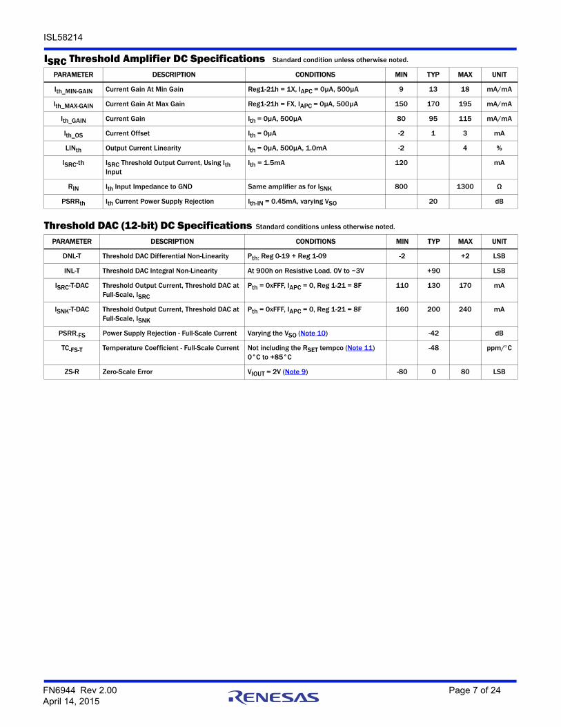
ISRC Threshold Amplifier DC Specifications. . . . . . . . . . . . . . . . . . . . . . . . . . . . . . . . . . . . . . . . . . . . . . . . . . . . . . . . . . . . . . . . . . . . . 7
Threshold DAC (12-bit) DC Specifications . . . . . . . . . . . . . . . . . . . . . . . . . . . . . . . . . . . . . . . . . . . . . . . . . . . . . . . . . . . . . . . . . . . . . . . 7
HFM (High Frequency Modulator) . . . . . . . . . . . . . . . . . . . . . . . . . . . . . . . . . . . . . . . . . . . . . . . . . . . . . . . . . . . . . . . . . . . . . . . . . . . . . . 8
Serial Interface AC Performance . . . . . . . . . . . . . . . . . . . . . . . . . . . . . . . . . . . . . . . . . . . . . . . . . . . . . . . . . . . . . . . . . . . . . . . . . . . . . . 8
Laser Driver AC Performance . . . . . . . . . . . . . . . . . . . . . . . . . . . . . . . . . . . . . . . . . . . . . . . . . . . . . . . . . . . . . . . . . . . . . . . . . . . . . . . . . 9
Application Block Diagram. . . . . . . . . . . . . . . . . . . . . . . . . . . . . . . . . . . . . . . . . . . . . . . . . . . . . . . . . . . . . . . . . . . . . . . . . . . . . . . . . . . 10
Timing Diagram . . . . . . . . . . . . . . . . . . . . . . . . . . . . . . . . . . . . . . . . . . . . . . . . . . . . . . . . . . . . . . . . . . . . . . . . . . . . . . . . . . . . . . . . . . . . 10
Typical Performance Curves . . . . . . . . . . . . . . . . . . . . . . . . . . . . . . . . . . . . . . . . . . . . . . . . . . . . . . . . . . . . . . . . . . . . . . . . . . . . . . . . . 11
Applications Information . . . . . . . . . . . . . . . . . . . . . . . . . . . . . . . . . . . . . . . . . . . . . . . . . . . . . . . . . . . . . . . . . . . . . . . . . . . . . . . . . . . . 12RSET Scaling . . . . . . . . . . . . . . . . . . . . . . . . . . . . . . . . . . . . . . . . . . . . . . . . . . . . . . . . . . . . . . . . . . . . . . . . . . . . . . . . . . . . . . . . . . . . . . . . . . . . 12Scaling DAC and ISLOPE Scaling . . . . . . . . . . . . . . . . . . . . . . . . . . . . . . . . . . . . . . . . . . . . . . . . . . . . . . . . . . . . . . . . . . . . . . . . . . . . . . . . . . . 12Color Output Current . . . . . . . . . . . . . . . . . . . . . . . . . . . . . . . . . . . . . . . . . . . . . . . . . . . . . . . . . . . . . . . . . . . . . . . . . . . . . . . . . . . . . . . . . . . . . 12Color Output Operation . . . . . . . . . . . . . . . . . . . . . . . . . . . . . . . . . . . . . . . . . . . . . . . . . . . . . . . . . . . . . . . . . . . . . . . . . . . . . . . . . . . . . . . . . . . 12HFM Operation . . . . . . . . . . . . . . . . . . . . . . . . . . . . . . . . . . . . . . . . . . . . . . . . . . . . . . . . . . . . . . . . . . . . . . . . . . . . . . . . . . . . . . . . . . . . . . . . . . 12Threshold Current . . . . . . . . . . . . . . . . . . . . . . . . . . . . . . . . . . . . . . . . . . . . . . . . . . . . . . . . . . . . . . . . . . . . . . . . . . . . . . . . . . . . . . . . . . . . . . . 12Power Consumption . . . . . . . . . . . . . . . . . . . . . . . . . . . . . . . . . . . . . . . . . . . . . . . . . . . . . . . . . . . . . . . . . . . . . . . . . . . . . . . . . . . . . . . . . . . . . 12Register Usage . . . . . . . . . . . . . . . . . . . . . . . . . . . . . . . . . . . . . . . . . . . . . . . . . . . . . . . . . . . . . . . . . . . . . . . . . . . . . . . . . . . . . . . . . . . . . . . . . . 12Memory Map . . . . . . . . . . . . . . . . . . . . . . . . . . . . . . . . . . . . . . . . . . . . . . . . . . . . . . . . . . . . . . . . . . . . . . . . . . . . . . . . . . . . . . . . . . . . . . . . . . . 12Register List . . . . . . . . . . . . . . . . . . . . . . . . . . . . . . . . . . . . . . . . . . . . . . . . . . . . . . . . . . . . . . . . . . . . . . . . . . . . . . . . . . . . . . . . . . . . . . . . . . . . 12
Scale DAC Block Diagram . . . . . . . . . . . . . . . . . . . . . . . . . . . . . . . . . . . . . . . . . . . . . . . . . . . . . . . . . . . . . . . . . . . . . . . . . . . . . . . . . . . . 17
Color Block Diagram . . . . . . . . . . . . . . . . . . . . . . . . . . . . . . . . . . . . . . . . . . . . . . . . . . . . . . . . . . . . . . . . . . . . . . . . . . . . . . . . . . . . . . . . 18
Detailed Timing Diagram . . . . . . . . . . . . . . . . . . . . . . . . . . . . . . . . . . . . . . . . . . . . . . . . . . . . . . . . . . . . . . . . . . . . . . . . . . . . . . . . . . . . 18
Threshold Block Diagram . . . . . . . . . . . . . . . . . . . . . . . . . . . . . . . . . . . . . . . . . . . . . . . . . . . . . . . . . . . . . . . . . . . . . . . . . . . . . . . . . . . . 19Threshold DAC . . . . . . . . . . . . . . . . . . . . . . . . . . . . . . . . . . . . . . . . . . . . . . . . . . . . . . . . . . . . . . . . . . . . . . . . . . . . . . . . . . . . . . . . . . . . . . . . . . 19Threshold Current . . . . . . . . . . . . . . . . . . . . . . . . . . . . . . . . . . . . . . . . . . . . . . . . . . . . . . . . . . . . . . . . . . . . . . . . . . . . . . . . . . . . . . . . . . . . . . . 19
Oscillator Block Diagram . . . . . . . . . . . . . . . . . . . . . . . . . . . . . . . . . . . . . . . . . . . . . . . . . . . . . . . . . . . . . . . . . . . . . . . . . . . . . . . . . . . . 20Oscillator Control . . . . . . . . . . . . . . . . . . . . . . . . . . . . . . . . . . . . . . . . . . . . . . . . . . . . . . . . . . . . . . . . . . . . . . . . . . . . . . . . . . . . . . . . . . . . . . . . 21HFM IOUT Equations. . . . . . . . . . . . . . . . . . . . . . . . . . . . . . . . . . . . . . . . . . . . . . . . . . . . . . . . . . . . . . . . . . . . . . . . . . . . . . . . . . . . . . . . . . . . . . 21HFM Frequency Counter . . . . . . . . . . . . . . . . . . . . . . . . . . . . . . . . . . . . . . . . . . . . . . . . . . . . . . . . . . . . . . . . . . . . . . . . . . . . . . . . . . . . . . . . . . 21
Serial Interface Protocol . . . . . . . . . . . . . . . . . . . . . . . . . . . . . . . . . . . . . . . . . . . . . . . . . . . . . . . . . . . . . . . . . . . . . . . . . . . . . . . . . . . . 22
Revision History. . . . . . . . . . . . . . . . . . . . . . . . . . . . . . . . . . . . . . . . . . . . . . . . . . . . . . . . . . . . . . . . . . . . . . . . . . . . . . . . . . . . . . . . . . . . 23
About Intersil . . . . . . . . . . . . . . . . . . . . . . . . . . . . . . . . . . . . . . . . . . . . . . . . . . . . . . . . . . . . . . . . . . . . . . . . . . . . . . . . . . . . . . . . . . . . . . 23
Package Outline Drawing . . . . . . . . . . . . . . . . . . . . . . . . . . . . . . . . . . . . . . . . . . . . . . . . . . . . . . . . . . . . . . . . . . . . . . . . . . . . . . . . . . . . 24
FN6944 Rev 2.00 Page 4 of 24April 14, 2015

ISL58214
IMPORTANT NOTE: All parameters having Min/Max specifications are guaranteed. Typical values are for information purposes only. Unless otherwisenoted, all tests are at the specified temperature and are pulsed tests, therefore: TJ = TC = TA
Absolute Maximum Ratings Thermal InformationVSO, Supply Voltages . . . . . . . . . . . . . . . . . . . . . . . . . . . . . . . . . . . . . . . . . . 6VVISNK, Voltage at ISNK . . . . . . . . . . . . . . . . . . . . . . . . . . . . . . . . . . . . . . . . . 7VISRC, Output Current. . . . . . . . . . . . . . . . . . . . . . . . . . . . . . . . . . . .1000mApkISNK, Output Current . . . . . . . . . . . . . . . . . . . . . . . . . . . . . . . . . . . . 600mApkVIH_DATA, Logic Input Voltages . . . . . . . . . . . . . . . . . . . . . .-0.5V to Lesser of . . . . . . . . . . . . . . . . . . . . . . . . . . . . . . . . . . . . . . . . . . . . . . . . VSO + 0.5V or 3VVIH, Logic Input Voltages . . . . . . . . . . . . . . . . . . . . . . . . . -0.5V to VSO + 0.5VIIN, Current into RSET, RFREQ, IAPC . . . . . . . . . . . . . . . . . . . . . . . . . . . . . 5mAESD Rating
Human Body Model (Tested per JESD22-A114E) . . . . . . . . . . . . . . . . 2kVMachine Model (Tested per JESD22-A115-A) . . . . . . . . . . . . . . . . . . 100VCharged Device Model . . . . . . . . . . . . . . . . . . . . . . . . . . . . . . . . . . . . 1500V
Latch Up (Tested per JESD-78B; Class 2, Level A) . . . . . . . . . . . . . . 100mA
Thermal Resistance (Typical) JA (°C/W) JC (°C/W)28 Ld QFN Package (Notes 4, 5) . . . . . . . . 37 2.9
TS, Storage Temperature Range. . . . . . . . . . . . . . . . . . . . .-60°C to +150°CPb-Free Reflow Profile . . . . . . . . . . . . . . . . . . . . . . . . . . . . . . . . . . see TB493
Recommended Operating ConditionsTA, Temperature Range . . . . . . . . . . . . . . . . . . . . . . . . . . . . . . -5°C to +85°CTJ, Junction Temperature . . . . . . . . . . . . . . . . . . . . . . . . . . . -5°C to +150°C
CAUTION: Do not operate at or near the maximum ratings listed for extended periods of time. Exposure to such conditions may adversely impact productreliability and result in failures not covered by warranty.
NOTES:
4. JA is measured with the component mounted on a high effective thermal conductivity test board in free air. See Tech Brief TB379 for details.
5. For JC, the “case temp” location is the center of the exposed metal pad on the package underside.
Electrical Specifications Unless otherwise indicated, all of the following tables are: VSO = VHI = 5V, RSET = 620Ω, RFREQ = 4700Ω, CLK = 100MHZ, RLOAD-ISRC = 8Ω to GND, RLOAD-ISNK = 10Ω to VHI, Scale DAC = 0x3FF, Reg 1-21 = 0x88, TA = +25°C.
PARAMETER DESCRIPTION MIN TYP MAX UNIT
DC ELECTRICAL SPECIFICATIONS
VSO (Notes 6, 7) 4.5 5.5 V
IVSO Supply Current (No Current Output) 25 40 mA
IS, dis Supply Currents, Disable Mode 10 15 mA
VISNK Allowable Operating Range of ISNK Pin (see Figure 2) 5.8 V
VIH_DATA Input Logic High Level for Data lines (D0-D9) 1.5 3 V
VIH Input Logic High Level 2.4 V
VIL Input Logic Low Level 0.8 V
VOH SDIO, Monitor Output High Level, IL = -5mA 2.4 V
VOL SDIO, Monitor Output Low Level, IL = 5mA 0.4 V
IINH Input Current High Level -1 +1 µA
IINL Input Current High Level, except ENA pin -1 +1 µA
IINL_ENA Input Current Low Level for ENA pin -15 -5 µA
NOTES:
6. Required voltage at the device pins. Allowance must be made for any voltage drop between the power supply and the device.
7. Required voltage also depends on laser diode manufacturer and pickup optical efficiency.
Scale DAC (10-bit) DC Specifications Standard conditions unless otherwise noted.
PARAMETER DESCRIPTION CONDITIONS MIN TYP MAX UNIT
DNL-PSCALE Differential Non-Linearity (Note 8) -3.5 +2.5 LSB
INL-PSCALE Integral Non-Linearity At 200h Resistive Load ~0V to ~3V +40 LSB
ZS-PSCALE Zero-Scale Error (Note 9) -2 0 +2 LSB
VRSET RSET Pin Voltage 1.03 1.06 1.11 V
NOTE:8. Differential non-linearity (DNL) is the differential between the measured and ideal 1 LSB change of any two adjacent codes.
FN6944 Rev 2.00 Page 5 of 24April 14, 2015

ISL58214
ISLOPE DC Specifications Standard conditions unless otherwise noted.
PARAMETER DESCRIPTION CONDITIONS MIN TYP MAX UNIT
RIN ISLOPE Input Impedance to GND 570 Ω
IGAIN SRC ISLOPE Current Gain to ISRC PSCALE = 0x3FF, Input Code = 0x3FF 450 mA/mA
IGAIN SNK ISLOPE Current Gain to ISNK PSCALE = 0x3FF, Input Code = 0x3FF 135 mA/mA
ISRC Color Power DAC (10-bit) DC Specifications Standard conditions unless otherwise noted.
PARAMETER DESCRIPTION CONDITIONS MIN TYP MAX UNIT
DNLCOLR_SRC Differential Non-Linearity -2 +0.5 LSB
INLCOLR_SRC Integral Non-Linearity 21 LSB
FSOUT-H1.1 Input code Full-Scale Output CurrentHeadroom = 1.1V
Input Code = 0x3FF, VISRC = 3.9V, VSO = 5.0V, RSET = 620Ω
625 mA
SFSOUT-
COLR_SRC
Full-Scale Current Power Supply Rejection vs VSO (Note 10) 40 dB
TFSOUT-
COLR_SRC
Full-Scale Current Temperature Coefficient (Note 11) 600 ppm/C
ZSCOLR_SRC Zero-Scale error VISRC = 2V (Note 9) -2 0 +2 LSB
ISNK Color Power DAC (10-bit) DC Specifications Standard conditions unless otherwise noted.
PARAMETER DESCRIPTION CONDITIONS MIN TYP MAX UNIT
DNLCOLR_SNK Differential Non-Linearity -4.9 +2.0 LSB
INLCOLR_SNK Integral Non-Linearity 60 LSB
FSOUT-620 Input code Full-Scale Output CurrentRSET = 620Ω, Reg 1-21 = 0x88
Input code = 0x3FF 200 250 mA
SFSOUT-
COLR_SNK
Full-Scale Current Power Supply Rejection vs VSO (Note 10) 20 dB
TFSOUT-COLR_SNK Full-Scale Current Temperature Coefficient (Note 11) 600 ppm/C
ZSCOLR_SNK Zero-Scale Error VISNK = 2V (Note 9) -8 0 +8 LSB
NOTES:9. Zero-scale error (ZS) is the deviation from zero current output when the digital input code is zero.
10. Full-scale output current power supply sensitivity (SFS) is measured by varying the VSO from 4.5V to 5.5V DC and measuring the effect of this signal on the full-scale output current.
11. Full-scale output current temperature coefficient (TFS) is given by delta (full-scale output current)/(T).
ISNK Threshold Amplifier DC Specifications Standard condition unless otherwise noted.
PARAMETER DESCRIPTION CONDITIONS MIN TYP MAX UNIT
Ith_MIN-GAIN Current Gain at Min Gain Reg1-21h = 1X, IAPC = 0µA, 500µA 8 17 25 mA/mA
Ith_MAX-GAIN Current Gain at Max Gain Reg1-21h = FX, IAPC = 0µA, 500µA 180 240 295 mA/mA
Ith_GAIN Current Gain Ith = 0µA, 500µA 80 135 170 mA/mA
Ith_OS Current Offset Ith = 0µA -2 1 3 mA
LINth Output Current Linearity Ith = 0µA, 500µA, 1.0mA -2 4 %
ISNK-th ISNK Threshold Output Current, Using Ith Input
Ith = 1.5mA 120 mA
RIN Ith Input Impedance to GND 800 1300 Ω
PSRRth Ith Current Power Supply Rejection Ith-IN = 0.45mA, varying VSO 20 dB
FN6944 Rev 2.00 Page 6 of 24April 14, 2015
ISL58214
ISRC Threshold Amplifier DC Specifications Standard condition unless otherwise noted.
PARAMETER DESCRIPTION CONDITIONS MIN TYP MAX UNIT
Ith_MIN-GAIN Current Gain At Min Gain Reg1-21h = 1X, IAPC = 0µA, 500µA 9 13 18 mA/mA
Ith_MAX-GAIN Current Gain At Max Gain Reg1-21h = FX, IAPC = 0µA, 500µA 150 170 195 mA/mA
Ith_GAIN Current Gain Ith = 0µA, 500µA 80 95 115 mA/mA
Ith_OS Current Offset Ith = 0µA -2 1 3 mA
LINth Output Current Linearity Ith = 0µA, 500µA, 1.0mA -2 4 %
ISRC-th ISRC Threshold Output Current, Using Ith Input
Ith = 1.5mA 120 mA
RIN Ith Input Impedance to GND Same amplifier as for ISNK 800 1300 Ω
PSRRth Ith Current Power Supply Rejection Ith-IN = 0.45mA, varying VSO 20 dB
Threshold DAC (12-bit) DC Specifications Standard conditions unless otherwise noted.
PARAMETER DESCRIPTION CONDITIONS MIN TYP MAX UNIT
DNL-T Threshold DAC Differential Non-Linearity Pth: Reg 0-19 + Reg 1-09 -2 +2 LSB
INL-T Threshold DAC Integral Non-Linearity At 900h on Resistive Load. 0V to ~3V +90 LSB
ISRC-T-DAC Threshold Output Current, Threshold DAC at Full-Scale, ISRC
Pth = 0xFFF, IAPC = 0, Reg 1-21 = 8F 110 130 170 mA
ISNK-T-DAC Threshold Output Current, Threshold DAC at Full-Scale, ISNK
Pth = 0xFFF, IAPC = 0, Reg 1-21 = 8F 160 200 240 mA
PSRR-FS Power Supply Rejection - Full-Scale Current Varying the VSO (Note 10) -42 dB
TC-FS-T Temperature Coefficient - Full-Scale Current Not including the RSET tempco (Note 11) 0°C to +85°C
-48 ppm/C
ZS-R Zero-Scale Error VIOUT = 2V (Note 9) -80 0 80 LSB
FN6944 Rev 2.00 Page 7 of 24April 14, 2015

ISL58214
HFM (High Frequency Modulator) Standard conditions unless otherwise noted.
PARAMETER DESCRIPTION CONDITIONS MIN TYP MAX UNIT
IMAX-ISRC-OFF Max HFM Off DC Output, ISRC HFMOFF = 0x7FF 90 120 160 mA
IMAX-SNK-OFF Max HFM Off DC Output, ISNK HFMOFF = 0x7FF 45 62 80 mA
IMIN-SRC-OFF Min HFM Off DC Output, ISRC HFMOFF = 0x000 -3 0 3 mA
IMIN-SNK-OFF Min HFM Off DC Output, ISNK HFMOFF = 0x000 -3 0 3 mA
IMAX-SRC-ON Max HFM Oscillator Output, ISRC HFMON = Reg 0-17h = 0xFF 118 mAP-P
IMAX-SNK-ON Max HFM Oscillator Output, ISNK HFMON = 0xFF Reg 1-21 = x8h
60 mAP-P
FOSC-MAX Max HFM Frequency Reg 0-16 = 0xFF; RFREQ = 4.7kΩ
850 980 1150 MHz
FOSC-MIN Min HFM Frequency Reg 0-16 = 0x01; RFREQ = 4.7kΩ
275 345 400 MHz
PSRROSC-AMP-ISNK PSRR - HFM Amplitude 700MHz; HFMON = 0xFF 1.2 %/V
TFOSC400MAX HFM Frequency Temperature Coefficient Range from 200MHz to 400MHz
0 - 900 ppm/C
TFOSC900MAX HFM Frequency Temperature Coefficient Range from 400MHz to 900MHz
±250 ppm/C
VRFREQ RFREQ Pin Voltage RFREQ = 4.7kΩ 0.85 1.01 1.1 V
SS-WIDTH-RANGE Spread Spectrum Spreading Width Adjustment Range
RFREQ = 4.7kΩReg 1-18 = 10h, Reg 0-16 = 0x26
0.1 0.293 1.1 %
SS_Shift Shift of Center Frequency when SS is Enabled vs when it’s Disabled
RFREQ = 4.7kΩReg 1-18-00h to 30h, Reg 0-16 = 26h
0.4 %
SS_Mod Spread Spectrum Modulation Frequency REG 1-18h Bit 7 = 0 30 53 80 kHz
SS_Mod Spread Spectrum Modulation Frequency REG 1-18h Bit 7 = 1 15 37 55 kHz
Serial Interface AC Performance Standard conditions unless otherwise noted.
PARAMETER DESCRIPTION CONDITIONS MIN TYP MAX UNIT
FSER SCLK Operating Range Static logic not limited at low frequency
0 50 MHz
tEH SEN “H” Time At 50MHz 320 ns
tEL SEN “L” Time At 50MHz 160 ns
tERSR SEN Rising Edge to the First SCLK Rising Edge At 50MHz 10 ns
tCDS SDIO Set-Up Time At 50MHz 10 ns
tCDH SDIO Hold Time At 50MHz 10 ns
tSREF Last SCLK Rising Edge to SEN Falling Edge At 50MHz 10 ns
tCC SCLK Cycle Time1 At 50MHz 20 ns
Duty SCLK “H” Duty Cycle At 50MHz 40 50 60 %
tCDD SDIO Output Delay At 50MHz 4 ns
tEDH SDIO Output Hold Time At 50MHz 2 ns
FN6944 Rev 2.00 Page 8 of 24April 14, 2015

ISL58214
Laser Driver AC Performance Demoboard test, 10% duty cycle pulse, load = equivalent circuitry to [laser + flex cable] and/or as noted. VSO = 5V. TA = +25°C.
PARAMETER DESCRIPTION CONDITIONS MIN TYP MAX UNIT
tR-ISRCx ISRC Write Rise Time (10% to 90%) Note 12 1.0 2.0 ns
tF-ISRCx ISRC Write Fall Time (10% to 90%) Note 12 1.0 2.0 ns
O/S-ISRCx ISRC Write Fast Overshoot Note 12 10 %
tR-ISNK ISNK Write Rise Time (10% to 90%) Note 12 0.8 1.5 ns
tF-ISNK ISNK Write Fall Time (10% to 90%) Note 12 0.5 1.0 ns
tDELAY From CLK at 50% to OUTPUT at 10% Note 12 4.5 ns
tOFF-DELAY From LOWP at 50% to OUTPUT at 10% Note 12 7 ns
tSETUP DATA to CLK 700 ps
tHOLD DATA to CLK 1500 ps
O/S-ISNK ISNK Write Fast Overshoot Note 12 10 %
BWIth Ith Amplifier 3dB Bandwidth Note 12 0.3 MHz
BWISLOPE ISLOPE Amplifier 3dB Bandwidth Note 12 3 MHz
NOTE:12. Limits established by characterization and are not production tested.
FN6944 Rev 2.00 Page 9 of 24April 14, 2015

ISL58214
Application Block Diagram
Timing Diagram
COLOR DAC
CONTROL AND
STATUS REGISTERS
SERIAL INTERFACE
SCALEDAC
THRESH DAC
REFERENCE BIAS AND POWER
SEN
SDIO
SCLK
RSET
ITH
GND
ISRC
VSO
VSO
GND
GNDB
ISNK
COLOR DAC2
GAIN REGISTER
BIAS
D0
D1
D2
D3
D4
D5
D6
D7
ISLOPE
CLK
D8
D9
LOWP
RFREQ
VSO
ENA
AMPLITUDE
FREQ
OSCAND
BUFFERSS
X
+
INPUT LATCH
A
INPUT LATCH
B
LOWP
01
1
0
D0 - D9
CLK
OUTPUT A B C
A B C D
LOWP
tDELAYtOFF DELAY
tSETUPtHOLD
FN6944 Rev 2.00 Page 10 of 24April 14, 2015

ISL58214
Typical Performance Curves
FIGURE 1. ISRC CURRENT vs VSD vs ISCALE_BIAS FIGURE 2. ISNK CURRENT vs VDS vs ISCALE_BIAS
FIGURE 3. HFM CONTROL FIGURE 4. HFM OSCILLATOR CURRENT CONSUMPTION
FIGURE 5. IOUT/ITH BANDWIDTH vs ITH FIGURE 6. IOUT/ISLOPE BANDWIDTH vs ISLOPE
3FFh
300h
200h
100h
80h
40h
0.0 0.5 1.0 1.5 2.0 2.5 3.0 3.5 4.0 4.50
200
400
600
800
1000
1200
(REG 1-21 = 88h) (VSO = 4.5V)
(RSET = 620Ω)
I SR
C(m
A)
VHEADROOM (V)
ISRC vs VHEAD vs SCALE CODE
0
100
200
300
400
500
0 1 2 3 4 5
VHEADROOM (V)
3FFh
300h
200h
100h
ISNK vs VHEAD vs SCALE CODE
(Reg 1-21 = 8Fh) (VSO = 5.0V)
(RSET = 620Ω)
I SN
K (
mA
)
200
400
600
800
1000
1200
0 32 64 96 128 160 192 224 256
HFMFREQ CODE (DEC)
FO
SC
(M
Hz)
RFREQ = 4700Ω
RFREQ = 3900Ω
90
70
60
40
30
80
50
PHFMON = 0xFF
HFM FREQUENCY (Hz)
200 400M 600M 800M 1G
ISO
CO
NS
UM
PT
ION
(m
A)
PHFMON = 0x01
PHFMON = 0x80
700
600
500
400
300
2000.0 0.6 1.2 1.8 2.4 3.0
IAPC (mA)
BA
ND
WID
TH
(k
Hz)
0.0 0.8 1.6 2.4 3.2 4.0
15
13
11
9
7
5
BA
ND
WID
TH
(M
Hz)
ISLOPE (mA)
FN6944 Rev 2.00 Page 11 of 24April 14, 2015

ISL58214
Applications InformationRSET ScalingThe datasheet values for threshold current, and fast current are based on an RSET of 620Ω when scaling DAC and input code are both set to full scale. The user may choose RSET to match the output current needs of the application.
Scaling DAC and ISLOPE Scaling The scale DAC is biased equivalently by either ISLOPE or IRSET (= VRSET/RSET). That is, 1mA of either bias current results in the same ISRC. In the figures of this section, Scaling DAC output current is used to represent current either into ISLOPE or out of RSET pins.
Color Output CurrentThe color output current capability for a typical part is shown in Figures 1 and 2. In addition to scaling DAC output, the amount of ISRC will be limited by the available headroom voltage at the ISRC pin.
Color Output Operation On the rising edge of CLK, the data on the Dn lines is captured. A single data bus can be shared by the three different ISL58214 chips. A separate CLK line is needed for each chip. After the data is loaded in all three colors, the rising edge of LOWP will clock the data from the first flip-flop and into the output flip-flop. Then the output current will be applied to the respective lasers at the same time.
HFM OperationThe HFM oscillator is provided to reduce speckle. The frequency range is determined by RFREQ. The actual frequency is controlled by a register. The HFM includes a spread spectrum function. The frequency of the spread spectrum oscillator and the amplitude of the frequency shift can be programmed.
Threshold CurrentThreshold current may be controlled by either the Threshold DAC or the Ith input. When set by PTHRESH register (Page 0, Addr 19h, Page 1, Addr 09h), Ith is limited to the data sheet value, whereas the ITH input will allow a significantly higher value to be obtained. The threshold DAC and ITH currents sum together producing an input voltage on the net resistance at the ITH pin.
Power ConsumptionThe primary power consumption is caused by the headroom voltage across the output stage (VSO - VISRC) x ISRC. In a power sensitive application, the VSO can be reduced below 5.0V (but above VSOgood), so long as sufficient headroom is available to obtain the desired output current. The chip power dissipation depends on the size of the heat sink because the die is attached to a metal plate that is exposed under the package.
Register UsageUpon power-up all registers are initialized to zero. All registers are read/writable unless otherwise specified.
Bit settings marked as “Reserved” or blank must not be used. They may be wired to legacy circuitry.
Memory MapThe address space is organized into three pages with 128 bytes each. Registers CR0, CR1, CR2, and STATUS, can be accessed from any page at the same addresses. The active page is selected via the PAGESEL bits in CR2.
Register ListControl Register 0. . . . . . . . . . . . . . . . . . . . . . . . . . . . . . . . . . . . . . . . RegX-00 Control Register 1. . . . . . . . . . . . . . . . . . . . . . . . . . . . . . . . . . . . . . . . RegX-01Control Register 2. . . . . . . . . . . . . . . . . . . . . . . . . . . . . . . . . . . . . . . . RegX-02Status Register . . . . . . . . . . . . . . . . . . . . . . . . . . . . . . . . . . . . . . . . . . RegX-03
Scale DAC High Order Bits. . . . . . . . . . . . . . . . . . . . . . . . . . . . . . . . . Reg0-15HFM Frequency Setting . . . . . . . . . . . . . . . . . . . . . . . . . . . . . . . . . . . Reg0-16HFM Amplitude Setting . . . . . . . . . . . . . . . . . . . . . . . . . . . . . . . . . . . Reg0-17Threshold Current High Order Bits . . . . . . . . . . . . . . . . . . . . . . . . . . Reg0-19Unlink Control . . . . . . . . . . . . . . . . . . . . . . . . . . . . . . . . . . . . . . . . . . . Reg0-21Control Register 3. . . . . . . . . . . . . . . . . . . . . . . . . . . . . . . . . . . . . . . . Reg1-08Threshold Current Low Order Bits. . . . . . . . . . . . . . . . . . . . . . . . . . . Reg1-09Slow Damping. . . . . . . . . . . . . . . . . . . . . . . . . . . . . . . . . . . . . . . . . . . Reg1-0AHFM Frequency Counter. . . . . . . . . . . . . . . . . . . . . . . . . . . . . . . . . . . Reg1-0EDevice ID . . . . . . . . . . . . . . . . . . . . . . . . . . . . . . . . . . . . . . . . . . . . . . . Reg1-15Revision ID. . . . . . . . . . . . . . . . . . . . . . . . . . . . . . . . . . . . . . . . . . . . . . Reg1-16Q Damping . . . . . . . . . . . . . . . . . . . . . . . . . . . . . . . . . . . . . . . . . . . . . Reg1-17Spread Spectrum Control . . . . . . . . . . . . . . . . . . . . . . . . . . . . . . . . . Reg1-18Threshold & Scale DAC Gain Select . . . . . . . . . . . . . . . . . . . . . . . . . Reg1-21Scale DAC Low Order Bits . . . . . . . . . . . . . . . . . . . . . . . . . . . . . . . . . Reg2-15IOUT Select. . . . . . . . . . . . . . . . . . . . . . . . . . . . . . . . . . . . . . . . . . . . . . Reg2-27
FN6944 Rev 2.00 Page 12 of 24April 14, 2015

ISL58214
Register Bit DescriptionTABLE 1. CR0: CONTROL REGISTER 0 (REG X-00)
BIT NAME BIT DEFINITION
B7 SELECT ISNK
Use in conjunction with Reg 2-27 Bit 1If B7 = 0 and Reg 2-27[1] = 0, ISRC is selected.If B7 = 1 and Reg 2-27[1] = 1, ISNK is selected.
B6-B2 Reserved Leave as 00000
B1 OELaser Output Enable1: Enable laser output stage.0: Disable laser output stage.
B0 CE
Chip Enable1: Enable device.0: Deep sleep, analog portion of the chip is powered down. SDIO still active.The ENA pin is ANDed with CE bit to generate internal Chip Enable.
TABLE 2. CR1: CONTROL REGISTER 1 (REG X-01)
BIT NAME BIT DEFINITION
B7 HFMCNTENHFM Counter Enable for measuring HFM frequency1: Enable HFM counter.0: Disable HFM counter (conserve power).
B6-B4 Reserved Leave 000
B3HFMOSCEN
HFM Oscillator Enable1: Enable.0: Disable.
B2-B0 Reserved Leave 000
TABLE 3. CR2: CONTROL REGISTER 2 (Reg X-02)
BIT NAME BIT DEFINITION
B7 Reserved Leave 0
B6 PAGEAUTOB6 = 0 means that the memory page will not auto toggle.B6 = 1 means that the Memory Page will Auto-toggle between Page0 and Page2.
B5B4
PAGESEL1PAGESEL0
Memory Page Select00: Set accessed page to Page 001: Set accessed page to Page 110: Set accessed page to Page 211: Reserved
B3-B0 Reserved Leave 0000
TABLE 4. SR1: STATUS REGISTER (REG X-03)
BIT NAME BIT DEFINITION
B7, B3 Reserved
B2 Color Enabled 1 means color current is enabled. 0 means color current is not enabled.
B1 reserved
B0 PWR OK1 means that both the 5V and internal 2.5V supplies are above the detection levels. 0 means that one or both supplies are below the detection levels. The detection levels are below the minimum specified.
TABLE 5. SCALE-H: POWER MAX HIGH (REG 0-15)
BIT NAME BIT DEFINITION
B7-B0 SCALE-H SCALE-H - High Order Bits Iw = k(512B7 +256B6 + .... +8B1 +4B0 + Reg 2-15)
FN6944 Rev 2.00 Page 13 of 24April 14, 2015

ISL58214
TABLE 6. HFMFREQ: HFM FREQUENCY SETTING (REG 0-16)
BIT NAME BIT DEFINITION
B7-B0 HFMFREQHFMFREQ = FMIN + FSTEP(128B7 +64B6 + 32B5 + 16B4 + 8B3 + 4B2 + 2B1 + B0)Note: If HFMFREQ = 00h, the HFM output is DC
TABLE 7. HFMON: HFM ON-AMPLITUDE (REG 0-17)
BIT NAME BIT DEFINITION
B7-B0 HFMONHFMON = k(128B7 +64B6 + 32B5 + 16B4 + 8B3 + 4B2 + 2B1 + B0) See “Oscillator Block Diagram” on page 20 for more details on the HFM amplitude.
TABLE 8. THRESHH: THRESHOLD CURRENT HIGH ORDER BITS (REG 0-19)
BIT NAME BIT DEFINITION
B7-B0 THRESHH THRESH = k(2048B7 +1024B6 + ... + 32B1 + 16B0 + THRESHL) THRESHL bits are in Reg 1-0A
TABLE 9. UNLINK: UNLINK CONTROL (REG 0-21)
BIT NAME BIT DEFINITION
B7 UnlinkIf unlink = 1, the SCALE DAC gets its reference from the ISLOPE pin only.If unlink = 0, the SCALE DAC gets its reference from the RSET pin and the ISLOPE pin.
B6-B0 Reserved Leave 0000000
TABLE 10. CR3: CONTROL REGISTER 3 (REG 1-08)
BIT NAME BIT DEFINITION
B7 REGRST
Resets all registers.1: Reset. Safety interlock allows reset bit to have effect only when lower three bits of CR0 are cleared (CE = OE = WE = 0).0: Normal operation.
B6-B0 Reserved
TABLE 11. THRESHL: THRESHOLD CURRENT LOW ORDER BITS (REG 1-09)
BIT NAME BIT DEFINITION
B7-B4 Reserved Leave 0000
B3-B0 THRESH-L THRESH-L = k(THRESH-H + 8B3 + 4B2 + 2B1 + B0), THRESH-H is Reg 0-19
TABLE 12. SLOW DAMPING CONTROL (REG 1-0A)
BIT NAME BIT DEFINITION
B7-B3 Reserved Leave 0000
B2-B0 SDAMP1 ISRC Write Waveform Damping
TABLE 13. HFM FREQUENCY COUNT REGISTER (READ MODE) (REG 1-0E)
BIT NAME BIT DEFINITION
B7 - B0 HFMCNTHFM cycles when SEN is high when HFM counting is enabled. B7 is the MSB. The counter will rollover if the count exceeds 255.Reg X-01, bit 7 = 1 enables the HFM counter. Reg 1-0E bit 1 enables the serial HFM counter.
FN6944 Rev 2.00 Page 14 of 24April 14, 2015

ISL58214
TABLE 14. HFM FREQUENCY COUNT REGISTER (WRITE MODE) (REG 1-0E)
BIT NAME BIT DEFINITION
B7 - B2 Reserved
B1 Enable Serial HFM CountIf B1 = 1, the HFM counter will count when SCLK is high.If B1 = 0, the HFM counter will not count.
B0 SCLK ModeIF B1 above = 1, and B0 = 0, SCLK is the interval for the HFM frequency count.If B1 above = 1, and B0 = 1, SCLK/2 is the interval for the HFM frequency count (two SCLK periods).
TABLE 15. DEVICE ID (REG 1-15)
BIT NAME BIT DEFINITION
B7 - B0 Device ID Device ID = 0x77 A different number is available for each chip family.
TABLE 16. REVISION ID (REG 1-16)
BIT NAME BIT DEFINITION
B7 - B0 Revision ID This Rev ID is 0xC8 A number to identify the member of the device family.
TABLE 17. WRITE Q DAMPING AND LD SAMPLE (REG 1-17)
BIT NAME BIT DEFINITION
B7 LD Sample EnaB7 = 1 means that laser voltage sampling is enabled.B7 = 0 means that laser voltage sampling is disabled.
B6 - B5 Reserved Do not use
B4 - B0 QD4 - QD0Write “Q” Damping for Iout1 is related to (16 QD4 + 8 QD3 + 4 QD2 + 2 QD1 + QD0). A larger number provides more damping.
TABLE 18. SPREAD SPECTRUM CONTROL (REG 1-18)
BIT NAME BIT DEFINITION
B7 SS Frequency and DisableIf bits B7, B6, B5, and B4 are all 0, the SS is disabled. If SS width is non zero, this bit selects about 34kHz when 1, and about 53kHz when 0.
B6 - B4 SS Width Width k (24B6 + 2 B5 + B4)
B3 - B0 Reserved Do not use
TABLE 19. THRESHOLD AND SCALE DAC GAIN SELECT (REG 1-21)
BIT NAME BIT DEFINITION
B7 - B4 ITHRESHOLD GAINThe Gain of the threshold amplifier is = K(8B7 + 4B6 + 2B5 + B4). The power-up register value is 1000. A setting of 0000 defaults to a setting of 0001 to prevent zero gain.
B3 - B0 ISNK_MAX
If ISNK output is selected, these 4 bits multiply by the existing SCALE output to determine the ISNK fast current. The power-up register value is 1000. A setting of 0000 defaults to a setting of 0001 to prevent zero gain.If ISRC is selected, these bits should be 0000.
FN6944 Rev 2.00 Page 15 of 24April 14, 2015

ISL58214
TABLE 20. SCALE-L: POWER MAX LOW (REG 2-15)
BIT NAME BIT DEFINITION
B7, B6 SCALE-L Read Only, these are the register bits.
B5, B4 Reserved Do not use
B3, B2 SCALE-LSCALE-L - Low Order Bits Iw = k(Reg 0-15 + 2B3 +B2) see SCALE-H in Table 5. When written these bits go the SCALE-L register. When read back, these are the SCALE DAC register bits.
B1, B0 Reserved Do not use
NOTE: The lower SCALE bits and the high SCALE bits are both written from their register to the SCALE DAC at the same time that the SCALE high bits are written to their register.
TABLE 21. IOUT SELECT (REG 2-27)
BIT NAME BIT DEFINITION
B7 - B2 Reserved Do not use
B1 Select ISNK
Use in conjunction with Reg X-00 Bit 7If B0 = 0 and Reg X-00[7] = 0, ISRC is selected.If B1 = 1 and Reg X-00[7] = 1, ISNK is selected.
B0 Reserved Leave 0
TABLE 22. THRESHOLD CURRENT DAC REPRESENTATION
Register bitsTHRESHH THRESHL
B7 B6 B5 B4 B3 B2 B1 B0 B3 B2 B1 B0
RepresentationUnsigned 12-bit
B11 B10 B9 B8 B7 B6 B5 B4 B3 B2 B1 B0
FN6944 Rev 2.00 Page 16 of 24April 14, 2015

ISL58214
Scale DAC Block Diagram
ISRC
ISNK
0
REG
1 -
21
1 2 3 4 5 6 7
SCALEDAC
76543210
REG
0 -
15
76543210
REG
2 -
15
7
REG 2 - 15
6 5 4 3 2 1 0
CLK
~1.2V
RSET
REG 0-21 BIT 7UNLINK
0
SNK_MAX
TO ISNK OSC OUTPUT
WRITE
READ
FROMCOLOR
CURRENTREGISTERS
Writing to Reg 2-15 goes to a temporary CLK. Writing to Reg 0-15 clocks both the Reg 2-15 temporary data and the Reg 0-15 data to the SCALE DAC.
TO ISRC OSC OUTPUTS
1
• All of the DAC’s are multiplying DAC’s, where the output is the product of the input code, and the applied reference signal.
ISLOPE
GND
ISLOPE
RIN
COLOR DAC
COLOR DAC2
+
-
+
-
FN6944 Rev 2.00 Page 17 of 24April 14, 2015

ISL58214
Color Block Diagram
Detailed Timing Diagram
MUX
ISRC
ISNK
0101
0011
ISRCxx
ISNK
3
SEL
10
SCALE DAC
REG X-00 [1]REG X-00 [0]
ENACOLOR ENABLE
REG 2-27 - 1REG X-00 - 7
0
REG
1 -
0A
1 2 3 4 5 6 7
ISRC SLOW DAMPING
0
REG
1 -
17
1 2 3 4 5 6 7
Q DAMPING
ISRC
SNK_MAX
LOWP
0
REG
1 -
21
1 2 3 4 5 6 7
D0
D1
D2
D3
D4
D5
D6
D7
CLK
D8
D9
INPUT LATCH
A
INPUT LATCH
B
01 1
0
COLOR DAC
COLOR DAC2
SCALE DAC
DATA
CLK
D-FF out
Latch A signal
Latch B signal
n n + 1 n + 2 n + 3 n + 4 n + 5
n n + 2 n + 4LATCH A
n + 1 n + 3 n + 5LATCH B
n n + 1 n + 2 n + 3 n + 4 n + 5MUX OUT
FN6944 Rev 2.00 Page 18 of 24April 14, 2015

ISL58214
Threshold Block Diagram
Threshold DACThe THRESH DAC outputs a positive current into the net resistance at the input of the ITH voltage-to-current converter amplifier. The external VTH independently creates a voltage at the input of the IAPC amplifier. The net voltage at the input of the IAPC amplifier divided by RIN is defined as the APC amplifier input current, even though the current is to ground. This input current multiplied by the specified gain ITHGAIN gives the output current IOUTTH. The Threshold amplifier gain varies from 0 to full scale proportional to Reg 1-21-(4-7).
The 12-bit THRESH DAC register is CLKed when THRESH-H is loaded to prevent glitches. It is designed to be a 12-bit monotonic DAC.
When Reg 1-21 = 80h, the gain from IAPC to IOUT is about 100mA/mA for any selected output channel.
If LOWP = 1, the threshold current is set to zero.
Threshold CurrentThe threshold current is approximately determined by interpolation from data specs.
IOUT-THRESH = IOUTTHRESH-DAC + IOUTTHRESH-Ith
Where:
• IOUTTHRESH-DAC ~= IOUT-R-DAC x THRESHMULT x RTH / (RTH + RIN)
• IOUTTHRESH-Ith ~= ITHGAIN x VTH-IN / (RTH + RIN)
Where:
IOUT-T-DAC Gives for example: 110mA.
RIN Gives for example: 1000 typ ohms.
ITH_GAIN Gives for example: 100 typ mA/mA.
THRESHMULT ~= THRESHDAC/4095, where THRESHDAC
The above equations assume a linear transfer function. At high currents there are saturation effects. Below 1V headroom, depending on the current, the predicted output will be less than predicted.
ISRC
ISNK
THRESHDAC
ITH
0
REG
1 -
21
4
The gain from IAPC to IOUT varies proportional to the
code in Reg 1-21(4-7)
VSO
1 2 3 4 5 6 7
N GAIN
0
REG
0 -
19
1 2 3 4 5 6 7
THRESH-HI
0
REG
1 -
09
1 2 3 4 5 6 7
THRESH-L
CLK
CLK
WRITE THRESH
RIN
VTH-IN
2
RegX-00bit70101
Reg2-27bit10011
ISRCxx
ISNK
LOWP
OUTPUT MIRROR DRIVER ISINK
VHI
VLASER
VHEAD
VSO
RTH
FN6944 Rev 2.00 Page 19 of 24April 14, 2015

ISL58214
Oscillator Block Diagram
RSET
Reg 0- 18[ 7:0 ]PHFMOFFH8
Reg 0- 09[ 7:4 ]PHFMOFFL4
8
Reg 0- 17[ 7:0 ]PHFMON8
Reg 1- 18[ 6:4 ] PHFMSS HFM SS
Reg 0- 16[ 7:0 ]PHFMFREQ
HFM FREQ
+
IRFREQ
HFMOSC
Reg X- 01[ 3 ]
MUX
OSC ENABLE
1
0
HFMDAC0
HFMDAC1
+
+
ISNK
ISRC
Reg X- 00[ 1 ]
Reg X- 00[ 7 ]
OUTPUT SELECT
HFM CNT/DIV
Reg X- 01[ 7 ]HFMCNT / HFMDIV256 ENABLE
Reg 1- 0E[ 7:0 ] (read)
12
8
Reg 1- 0E[ 0 ]
DIV/2
Reg 1- 0E[ 1 ]0
1
HFM Freq = HFMCNT * SCLK
1 or 2
valid only when HFMCNT ENABLE is SET
SCLK
SCALE PRESCALE
Reg 1- 21[ 3:0 ]
ISLOPE
ISET
4
BAND GAP
0
1
UNLINK
Reg 0- 21[ 7 ]
Reg 2- 27[ 1 ] ISNK EN
ISNK SELECTOUTPUTEN
SPANFREQReg 1- 18[ 7 ]
Reg 0- 15[ 7:0 ]
Reg 2- 15[ 2:3 ]
8
2
10
+
DAC
THRESHOLD BLOCK
SEL
FN6944 Rev 2.00 Page 20 of 24April 14, 2015

ISL58214
Oscillator ControlA high frequency component can be added to the laser current to reduce speckle.
The HFM block has two states determined by whether the oscillator is enabled or disabled. The HFM block outputs RF modulation when the oscillator is enabled and a DC level when the oscillator is disabled. The DC level is PHFMOFF in HFMOFF mode.
HFM IOUT EquationsThe oscillator current is approximately determined by interpolation from the datasheet.
IOUTOSC-ON AON,max x PHFMON/255 x KREF OR Zero.
Where:
• AON,max = for example: 100mA (typ).
• KREF = (RSETSPEC/RSET)
• RSETSPEC = for example 620Ω.
When the HFM oscillator is turned on, the oscillator current reaches a peak value set by PHFMON. The relation between PHFMON and average optical power is difficult to derive deterministically. First, the AC current reaching the laser is attenuated by parasitics. The higher the HFM frequency, the larger the loss. Second, if the laser is biased near threshold, the turn-on delay reduces the optical pulse width. Third, laser relaxation oscillation further shapes the optical pulse.
An empirical procedure is to first find the best conditions for the AC current (PHFMON) and frequency (HFMFREQ) in terms of read noise reduction.
HFM Frequency CounterHFM frequency can be monitored via internal counter. The way to monitor the HFM frequency is to measure how many cycles occur during a serial clock period. If the serial clock period is known, this enables the HFM to be measured and adjusted by the drive firmware. To enable this measurement, follow the following steps:
• First clear Reg X-01 Bit 7 = 0. This allows the serial port to use the control register at Reg 1-0E.
• Set Reg 1-0E bit 1 = 1. This enables the serial clock to gate the counter.
• Set Reg1-0E bit 0 = 1. This step is optional, but recommended. This would divide the serial clock by 2, hence increase the number of count of cycles by 2. Since SEN is not synchronized with the HFM, higher number of counts means lower the error.
• Set Reg X-01 bit 7 = 1. This allows the control logic to measure the burst of HFM between serial clock edges. The control logic will continue to do this on any serial transfer, either a write or a read. The measurement is done during the address portion of the serial cycle.
• By reading Reg 1-0E, the measurement is done.
• The HFM frequency then can be calculated as HFM frequency = HFMCNT(dec) x known SCLK/2.
The amount of HFM current that reaches the laser and produces light modulation is a very complex transfer function. Although the HFM circuit simply switches between zero and the specified current, the frequency is so high that the result is heavily influenced by the chip, packages and layout.
TABLE 23. OSCILLATOR CONTROL LOGIC
X-01-3 OSCILLATOR OUTPUT
0 Off
1 On
FN6944 Rev 2.00 Page 21 of 24April 14, 2015

ISL58214
Serial Interface Protocol
WRITING CYCLE INTO ISL58214
D0
D1
D2
D3
D4
D5
D6
D7
A0
A1
A2 A3
A4
A5
A6
0
tCDS tCDH
tCC tCH
tCL
tERSR
SEN
SCLK
SDATA
tSREF
R/W BIT, ADDRESS BITS, AND DATA BITS ARE CLOCKED INTO ISL58214 AT RISING EDGE OF SCLK.
R/W
READING CYCLE FROM ISL58214
D0
D1
D2
D3
D4
D5
D6
D7
A0
A1
A2 A3
A4
A5
A6
1
tCDS tCDH
tCC tCH
tCL
tERSR
SEN
SCLK
SDATA
tSREF
Hi-Z
tCDD
R/W BIT AND ADDRESS BITS ARE CLOCKED INTO ISL58214 AT RISING EDGE OF SCLK. DATA BITS ARE CLOCKED OUT FROM ISL58214 AT FALLING EDGE OF SCLK. THE LAST BIT (D0) OF DATA IS CLOCKED BY THE FALLING EDGE OF SEN.
tEH
tEH
tEL
tEL
FN6944 Rev 2.00 Page 22 of 24April 14, 2015

ISL58214
Intersil products are manufactured, assembled and tested utilizing ISO9001 quality systems as notedin the quality certifications found at www.intersil.com/en/support/qualandreliability.html
Intersil products are sold by description only. Intersil may modify the circuit design and/or specifications of products at any time without notice, provided that such modification does not, in Intersil's sole judgment, affect the form, fit or function of the product. Accordingly, the reader is cautioned to verify that datasheets are current before placing orders. Information furnished by Intersil is believed to be accurate and reliable. However, no responsibility is assumed by Intersil or its subsidiaries for its use; nor for any infringements of patents or other rights of third parties which may result from its use. No license is granted by implication or otherwise under any patent or patent rights of Intersil or its subsidiaries.
For information regarding Intersil Corporation and its products, see www.intersil.com
For additional products, see www.intersil.com/en/products.html
© Copyright Intersil Americas LLC 2010-2015. All Rights Reserved.All trademarks and registered trademarks are the property of their respective owners.
About IntersilIntersil Corporation is a leading provider of innovative power management and precision analog solutions. The company's products address some of the largest markets within the industrial and infrastructure, mobile computing and high-end consumer markets.
For the most updated datasheet, application notes, related documentation and related parts, please see the respective product information page found at www.intersil.com.
You may report errors or suggestions for improving this datasheet by visiting www.intersil.com/ask.
Reliability reports are also available from our website at www.intersil.com/support
Revision HistoryThe revision history provided is for informational purposes only and is believed to be accurate, but not warranted. Please go to web to make sure you have the latest Rev.
DATE REVISION CHANGE
April 1, 2015 FN6944.2 Removed Related Literature from page 1.Stamped Datasheet Not Recommended for New Designs No Recommended Replacement.
July 29, 2013 FN6944.1 Converted to New Intersil Template. Changed Products information to About Intersil.
May 13, 2010 FN6944.0 Initial Release
FN6944 Rev 2.00 Page 23 of 24April 14, 2015

ISL58214
FN6944 Rev 2.00 Page 24 of 24April 14, 2015
Package Outline Drawing
L28.4x5A28 LEAD QUAD FLAT NO-LEAD PLASTIC PACKAGERev 2, 06/08
C 0 . 2 REF
0 . 05 MAX.0 . 00 MIN.
5
4.00 A
B
5.00
(4X) 0.15
6
PIN 1INDEX AREA
23PIN #1 INDEX AREA
28
2.50
24X 0.50
Exp. DAP
8
122
14
28X 0.400
9
6
3.50
Max 0.90
SEE DETAIL "X"
SEATING PLANE0.08
0.10C
C
C
( 4.80 )
( 3.50 )
( 28 X 0.60)
(28X .250)
( 24X 0.50)
( 3.80 )
( 2.50)
2.50
0.10
28X 0.25
AM C B
4
3.50
Exp. DAP
15
TYPICAL RECOMMENDED LAND PATTERN
DETAIL "X"
TOP VIEW
BOTTOM VIEW
SIDE VIEW
SIDE VIEW
located within the zone indicated. The pin #1 identifier may be
Unless otherwise specified, tolerance : Decimal ± 0.05
Tiebar shown (if present) is a non-functional feature.
The configuration of the pin #1 identifier is optional, but must be
between 0.15mm and 0.30mm from the terminal tip.
Dimension b applies to the metallized terminal and is measured
Dimensions in ( ) for Reference Only.
Dimensioning and tolerancing conform to AMSE Y14.5m-1994.
6.
either a mold or mark feature.
3.
5.
4.
2.
Dimensions are in millimeters.1.
NOTES: