Embed Size (px)
Citation preview
f fo ' l l ,r*:('
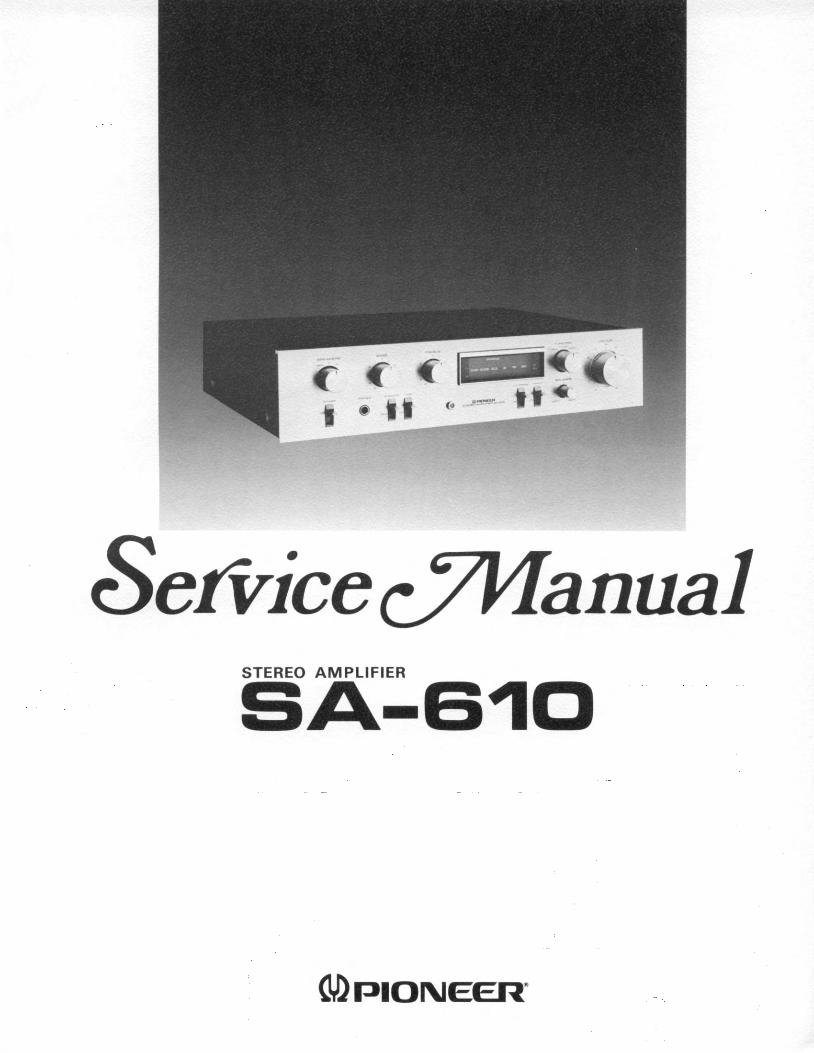
EefvicecVlanualS T E R E O A M P L I F I E R
S \-Ci,lO
()rrroruEErl'
o This service manual is applicable to the KU type.
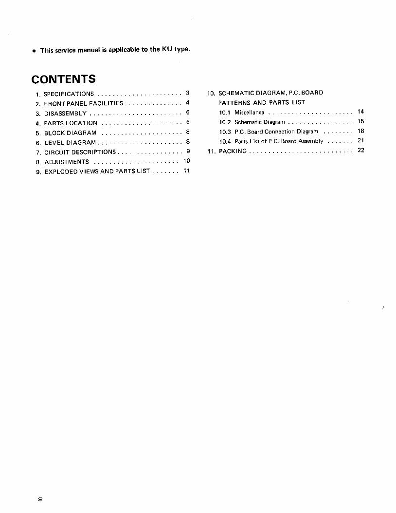
CONTENTSI . S P E C I F I C A T | O N S . . . . . . . 3
2 . F R O N T P A N E L F A C I L I T I E S . . . . . 4
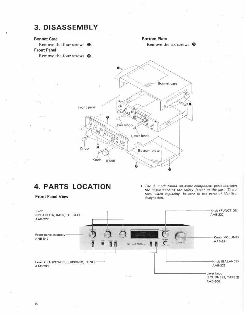
3 . D I S A S S E M B L Y . . . . 6
4 . P A R T S L O C A T I O N . . . . . . 6
5 . B L O C K D I A G R A M . . . . . . 8
6 . L E V E L D I A G R A M . . . . . . . 8
T . C T R C U I T D E S C R I P T I O N S . . . . . . ' 9
S . A D J U S T M E N T S . . . . . . 1 0
9 . E X P L O D E D V I E W S A N D P A R T S L I S T . . . . . . . 1 1
10 . SCHEMATIC D IAGRAM, P .C . BOARD
PATTERNS AND PARTS LIST
1 0 . 1 M i s c e l l a n e a ' . - . . ' . 1 4
10.2 Schemat ic Diagram 15
10.3 P.C. Board Connect ion Diagram 18
10.4 Parts List of P.C. Board Assembly 21
1 1 . P A C K I N G . . . . . . . 2 2
(
r
I
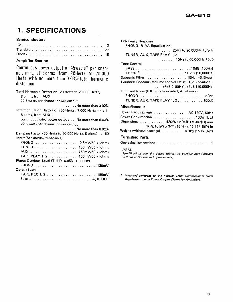
1 . SPECIF ICATIONSSemiconductorslCsTransistors 27D i o d e s . . . . . . 1 8
Amplifier Section
Cont inuous p0wer output of 45watts* per chan-ne l , m in . , a t 8ohms f rom 20Her tz to 20 ,000Hertz wi th no more than 0. \3%total harmonicd is to r t ion .Total Harmonic Distortion (20 Hertz to 20,000 Hertz,
I ohms, f rom AUX)22.5 watts per channel'power output
.No more than 0.02%Intermodulation Distortion (50 Hertz : 7,000 Hertz= 4 : 1
8 ohms, f rom AUX)continuous rated power output . . No more than 0.03%22.5 watts per channel power output
No more than O.O2%Damping Factor (2OHertz to 20.000 Hertz, S ohms) . . 50I nput (Sensitivity/lmpedance)
P H O N O . . . . 2 . 5 m V / 5 0 k i l o h m sTUNER 150mV/50 k i lohmsA U X . . . . . 1 5 0 m V / 5 0 k i l o h m sTAPE PLAY 1 ,2 . . 150mV/50 k i lohms
Phono Over load Level (T.H.D. O.O5o/o, 1.000H2)PHONO 130mV
Output (Level )
T A P E R E C l , 2 . . . . . 1 5 0 m VS p e a k e r . . . . A , B , O F F
siA-ci1 cl
Frequency ResponsePHONO (R IAA Equal izat ion)
TUNER, AUX, TAPE PLAY20Hz to 20.000H210.3d8
1 . 2. . 1OHz to 60,000H2 13dB
Tone ControlB A S S . . . t 1 0 d B ( 1 0 0 H 2 )T R E B L E . . . . t 1 0 d B ( 1 0 , 0 0 0 H 2 )
Subsonic Filter . . 15Hz (-6dB/oct)Loudness Contour (Volume contro l set at -40dB posi t ion)
. . . . +6dB (100H2), +3dB (10,000H2)Hum and Noise ( lHF, shor t -c i rcu i ted, A network)
P H O N O . . . 8 2 d BT U N E R , A U X , T A P E P L A Y 1 , 2 . . , . . . I O O d B
MiscellaneousPower Requirements AC 120V,60H2P o w e r C o n s u m p t i o n . . . 1 0 0 W ( U L )Dimensions . 42O(Wl x 94(H) x 347(D) mm
1 6 - 9 / 1 6 ( W ) x 3 - 1 1 l 1 6 ( H ) x 1 3 - 1 1 / 1 6 ( D ) i nWeight (wi thout package) 6.9kg (15 lb 3oz)
Furnished PartsO p e r a t i n g l n s t r u c t i o n s . . . . . . . . 1
NOTE:Specifications and the design subject to possible modificationswithout notice due to improvements.
* Measured pursuant to the Federal Trade Commission,s TradeRegulation rule on Power Output Claims for Amplifiers.
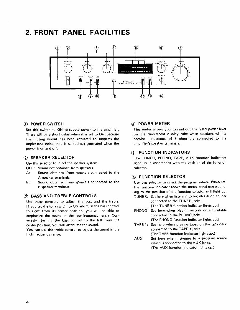
2. FRONT PANEL FACIL IT IES
O POWER SWITCHSet this switch to ON to supply power to the amplif ier.There wil l be a short delay when it is set to ON. becausethe muting circuit has been actuated to suppress the
unpleasant noise that is sometimes generated when thepower is on and off .
@ SPCETER SELECTORUse this selector to select the speaker system.OFF: Sound not obta ined f rom speakers.A: Sound obtained from speakers connected to the
A speaker terminals.B: Sound obtained from speakers connected to the
B speaker terminals.
@ BASS AND TREBLE CONTROLSUse these controls to adjust the bass and the treble.lf you set the tone switch to ON and turn the bass controlto right from its center position, you wil l be able toemphasize the sound in the low-f requency range. Con-versely, turning the bass control to the left from thecenter posi t ion, you wi l l a t tenuate the sound.You can use the treble control to adjust the sound in thehigh-frequency range.
@ POWER METERThis meter allows you to read out the rated power level
on the fluorescent display tube when speakers with a
nominal impedance of 8 ohms are connected to the
ampl i f ier 's speaker terminals.
@ FUNCTTON INDICATORSThe TUNER, PHONO, TAPE, AUX funct ion indicators
light up in accordance with the position of the function
se lector.
@ FUNCTION SELECTORUse this selector to select the program source. When set.
the function indicator above the meter panel correspond-
ing to the posi t ion of the funct ion selector wi l l l ight up.
TUNER: Set here when l is tening to broadcasts on a tuner
connected to the TUNER jacks.(The TUNER funct ion indicator l ights up.)
PHONO: Set here when p lay ing records on a turntableconnected to the PHONO jacks.(The PHONO funct ion indicator l ights up.)
TAPE 1: Set here when p lay ing tapes on the tape deck
connected to the TAPE 1 jacks.(The TAPE function indicator l ights up.)
AUX: Set here when listening to a program sourcewhich is connected to the AUX jacks.(The AUX funct ion indicator l ights up.)
riIi
O volurvrE coNTRoLUse this control to adjust the output level to the speakersand headphones. Turn it clockwise to increase the outputlevel . No sound wi l l be heard i f you set i t to , ,0 . , '
@ nCRopHoNE JAcKPlug the headphones into this jack when you want tol isten through your stereo headphones.
NOTE:Set the speaker selector to OFF when listening only with head-phones.
€) suesoNtc FTLTER SWTTCHWhen this switch is set to the ' l 5Hz position, the subsonicfi lter with a cut-off frequency of 15Hz is actuated. Thesubsonic fi l ter serves to attenuate frequencies lower than15Hz in a 6dB/oct slope. lt is therefore effective insuppressing ultra-low-frequency noise which is generatedby record warp and other causes. You cannot actuallyhear this noise but it is a factor in the generation ofintermodulation distortion and it may damage yourspeaker system. Set this switch to the 1SHz positionduring record play for the best effect.
@ rorue swtrcHSet this switch to ON when adjusting the bass and treblecontrols. When set to the upper (OFF) position, the tonecontrol circuits are disengaged and frequency response isflat. This function is convenient for checking phono car-tridge and speaker tone quality and listening roomacoustics.
@ powen tNDtcAToRWhen the power switch is set to ON this lamp lights up,indicat ing the ampl i f ier is turned on.
sA-Ci1cl
@ LouolrrEss swtrcHWhen listening to a performance with the volume controlturned down, set this switch to ON and the bass andtreble wil l be accentuated.When the volume is low, the human ear f inds i t harderto hear the bass and treble than when the volume is high.The loudness switch is thus designed to compensate forthis deficiency. By setting it to ON, the bass and treblecome through much more strongly and the sound takes ona punch even when the volume control is turned down.
@ rnpe 2 swrTcHSet this switch to the ON posit ion when monitoring a tapeperformance on a tape deck which you have connected tothe TAPE 2 jacks or when mon i to r ing a record ing .
NOTE:Set the switch to the upper (OFF) position when tistening torecords or broadcasts, etc. selected by the function selector.
@ BalarucE coNTRoLUse this control to balance the volume of the left andr ight channels. l f the sound appears to be louder on ther ight , i t means that the volume of the r ight channel ishigher. Turn the balance control to the left and adjust.Conversely, if the sound appears to be louder on the left,it means that the volume of the left channel is higher.Therefore, turn the balance control to the right andadjust.
I
I
f'
rt-
3. DISASSEMBLY
Bonnet CaseRemove the four screws
Front PanelRemove the four screws
o .
e .
Bottom PlateRemove the six screws O.
o The !i, marh found on some component parts indicatesthe importance of the safety factor of the part. There'
fore, when replacing, be sure to use parts of identicaldesignation.
4. PARTS LOCATIONFront PanelView
m(t .J!g!r.-
Knob (BALANCEI
AAB.223
Lever knob(LOUDNESS, TAPE 2)AAD.2OO
\o..oo/o' Bonnet case
Front panel
6
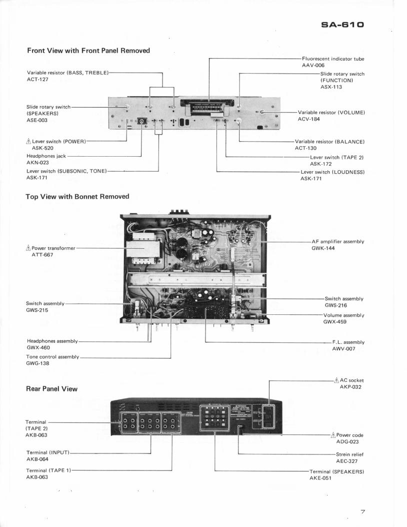
Front View with Front Panel Removed
Var i ab le r es i s t o r (BASS. TREBLE)ACT-127
I Lever swi tch (POWER]
ASK.520
Headphones . jackAKN-023
Leve r sw i t ch (SUBSONIC , TONE)ASK-1 71
Top View with Bonnet Removed
j Power t ransformerATT-667
Switch assemblyGWS-215
Headphones assemblyGWX460
Tone control assemblyGWG-138
Rear Panel View
Term ina l { INPUT)AK8.064
Te rm ina l (TAPE 1 )AKB-063
'! 'tlr '
rl|r
' l t u "I
Var i ab le r es i s t o r ( BA LANCE)ACT-130
-Lever sw i tch (TAPE 2)
s i A - 6 1 0
Fluorescent indicator tubeAAV-O06
Sl ide rotary swi tch( F U N C T I O N )
A S X - I 1 3
I o L:- - -Var iable resistor (VOLUME)€
A S K . 1 7 2
Lever swi tch ( LOUDN ESS)A S K - 1 7 1
AF amp l i f i e r assemb lyGWK.144
Switch assemblyGWS-216
Volume assemblyGWX459
I AC sockerAKP.O32
1i Power codeADG-023
Strein re l ie lAEC-327
Te rm ina l (SPEAKERS)
AKE-051
f
t-t
sl ide rota ry r*i t"tr -------]-=---.'
(SPEAKERS) I " :
ASE-oo3 | ,, ll
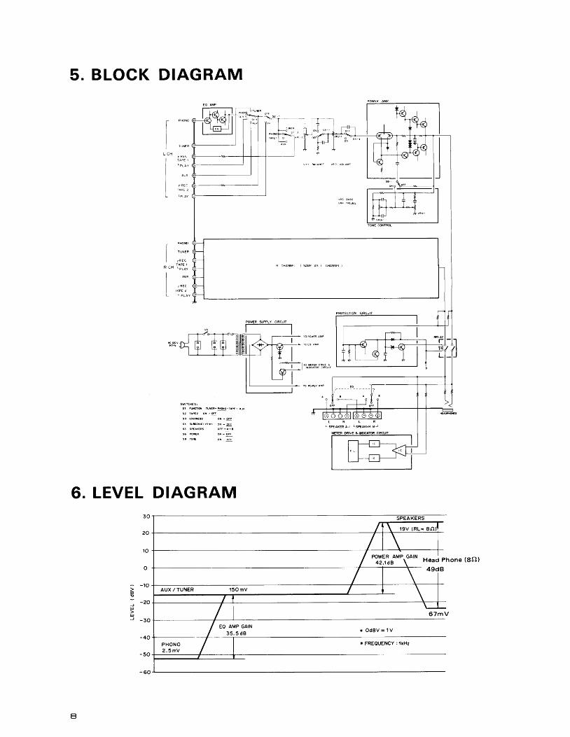
5. BLOCK DIAGRAM
swtrcHEs:st Fu&trox luxEP-M-raPEI-AUX32 fAPE? ON - 6F
t3 ouoi€ls ox - gll
54 Su6o i r t ( t5Hr l Ox - 6
55 SPEAXERS O'F-A- '
s6 &s€R ox -!Il
se ioilE or _lI!
6. LEVEL DIAGRAM
l}.tlJ"roo't xeai pnone (eo)
A U X / T U N E R 1 5 O m V
n 7 . C IRCUIT DESCRIPT IONS
Equal izer Ampl i f ierThe 54,-610 features a 3-stage direct-coupled
equalizer amplifier for greater reduction of noiseand distortion.
Besides the use of an ultra low-noise transistor(25C26O2) in the first stage, the adoption of lowimpedance input resistance and equalizer circuithas contributed to an S/N ratio of at least 82dB(at 2.5mV input, IHF-A).
Power AmplifierThis all stage direct-coupled pure complemen-
taly SEPP circuit features a current mirror loaddifferential amplifier in the first stage, and incor-porates the tone control circuit in the NFB loop.
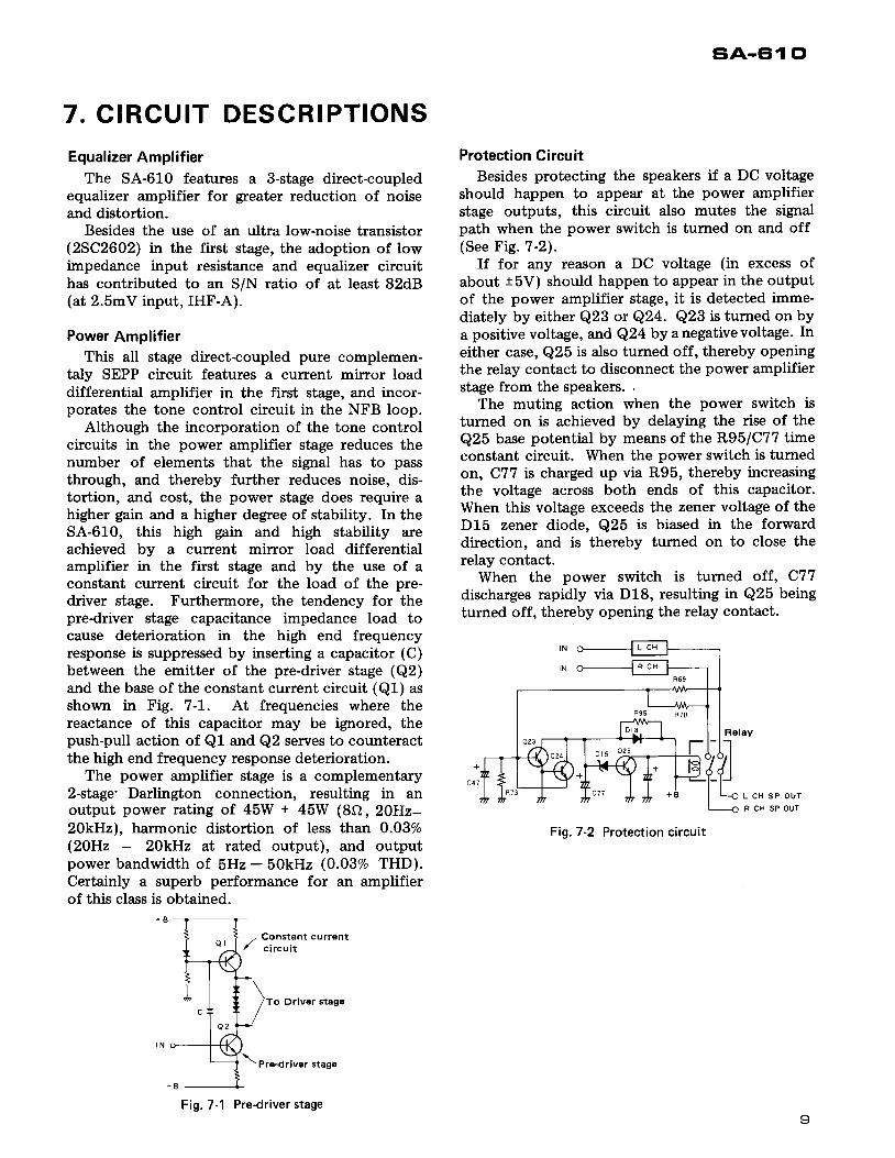
Although the incorporation of the tone controlcircuits in the power amplifier stage reduces thenumber of elements that the signal has to passthrough, and thereby further reduces noise, dis-tortion, and cost, the power stage does require ahigher gain and a higher degtee of stability. In theSA-610, this high gain and high stability areachieved by a cunent mirror load differentialamplifier in the first stage and by the use of aconstant current circuit for the load of the pre-driver stage. Furthermore, the tendency for thepre-driver stage capacitance impedance load tocause deterioration in the high end frequencyresponse is suppressed by inserting a capacitor (C)between the emitter of the pre-driver stage (Q2)and the base of the constant current circuit (Q1) asshown in Fig. 7-1. At frequencies where thereactance of this capacitor may be ignored, thepush-pull action of Ql and Q2 serves to counteractthe high end frequency response deterioration.
The power amplifier stage is a complementary2-stage' Darlington connection, resulting in anoutput power rating of 45W + 45W (8Q, 20Hz-2OkHz\, harmonic distortion of less than O.O37o(20H2 20kHz at rated output), and outputpower bandwidth of 5Hz - 50kHz (0.O3% THD).Certainly a superb performance for an amplifierof this class is obtained.
/. Constant current/ c i rcu i t
)to o,,u., . .r"n"
\Pre-driver staga
siA-61 cl
Protection CircuitBesides protecting the speakers if a DC voltage
should happen to appear at the power amplifierstage outputs, this circuit also mutes the signalpath when the power switch is turned on and off(See Fig. 7-2).
If for any reason a DC voltage (in excess ofabout tbV) should happen to appear in the outputof the power amplifier stage, it is detected imme-diately by either Q23 or q24. qn is turned on bya positive voltage, and Q24 by a negative voltage. Ineither case, Q25 is also turned off, thereby openingthe relay contact to disconnect the power amplifierstage from the speakers. ,
The muting action when the power switch isturned on is achieved by delaying the rise of theQ25 base potential by means of the R95/C77 timeconstant circuit. When the power switch is turnedon, C77 is charged up via R95, thereby increasingthe voltage across both ends of this capacitor.When this voltage exceeds the zener voltage of theD15 zener diode, Q25 is biased in the forwarddirection, and is thereby tumed on to close therelay contact.
When the power switch is turned off., C77discharges rapidly via D18, resulting in Q25 beingturned off, thereby opening the relay contact.
L C H S P O U T
R CH SP OUT
Fig. 7-2 Frotection circuit
!f'
r l
I
f,
I
i F
Fig. 7-1 Pre-driver stage
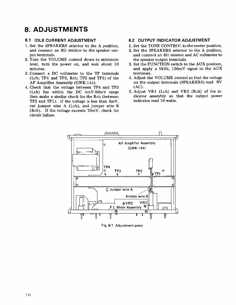
8. ADJUSTMENTS8.1 IDLE CURRENT ADJUSTMENT1. Set the SPEAKERS selector to the A position,
and connect an 8Q resistor to the speaker out-put terminals.
2. Turn the VOLUME control down to minimumlevel, turn the power on, and wait about 10minutes.
3. Connect a DC voltmeter to the TP terminals(Lch; TP4 and TP3, Rch; TP2 and TP1) of theAF Amplifier Assembly (GWK-144).
4. Check that the voltage between TP4 and TP3(Lch) lies within the DC 4mV-50mV rangethen make a similar check for the Rch (betweenTP2 and TP1). If the voltage is less than 4mV,cut jumper wire A (Lch), and jumper wire B(Rch). If the voltage exceeds 70mV, check forcircuit failure.
8.2 OUTPUT INDICATOR ADJUSTMENT1. Set the TONE CONTROL to the center position.2. Set the SPEAKERS selector to the A position,
and connect an 8O resistor and AC voltmeter tothe speaker output terminals.
3. Set the FUNCTION switch to the AUX position,and apply a 7kHz, 150mV signal to the AUXterminals.
4. Adjust the VOLUME control so that the voltageon the output terminals (SPEAKERS) read 9V(AC) .
5. Adjust VR1 (Lch) and VR2 (Rch) of the in-dicator assembly so that the output powerindicator read 10 watts.
AF Amplif ier Assembly(GWK-144 )
@ Jumper wire A
Jumper
-- l @vR2 vR1F.L Meter Assembly e
Fig. 8-1 Adjustment point
1 0
sA-61 cl
r 9. EXPLODED VIEWS AND PARTS LISTExterior Component
fa
I
f-'
Parts List
NOTE:c Parts without part number cannot be supplied.o The A marh found on some component parts indicates the importance of the
safety factor of the part. Therefore, when replacing, be sure to use parts of id.enti-cal designation.
Key No. Part No. Description
f,
1 .2 .3 .4 .5.
6 .7 .8.9 .
1 0 .
ANE.269ABA-079AAD.2OOAN8.847AAB.222
AAB.223AAB.221ABA-186
AB4-066
Bonnet caseScrewLever knobFront panel assemblyKnob
KnobKnob
ScrewBottom plate
Screw
.4.t4' - : ' \
1;r
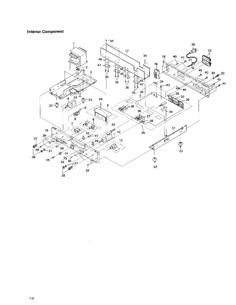
Interior Component
l K ' ?um;l _^s-il
Y'2o44
2930
32 34
- - 36,2ssl-
ffu..QN f - ,
ro '9;i,
w38
Y
siA-cil o
tt^ Parts List
Key No. Part No. Description Key No. Part No. Description
|'^
x-
l\ 1. 4rT-6672.3 .4. GWS-215
A s. AsK-s2o
A e. Acc-ool7. GWX4608. GWG-I389. AWV{07
1 0 .
1 1 .12 . GWS-21613. GWX-4591 4 .15. AEL-320
1 6 .1 7 .
A rg. AKP-0321 9 .
Azo. ADG-o23
21 . AEC-32722. AKE-O5123.
Azc . AEK- Ioo25. GWK-I44
Power transformer
Wire c l ipFrame
Switch assemblyLever switch
CapacitorHeadphones assemblyTone control assemblyF.L. assemblyCushion
LED socketSwitch assemblyVolume assemblyCushion rubberLED
Panel stayHeat s inkAC socketRear panelPower code
Strein re l ief
TerminalTe rm ina l (GND)
Fuse
AF ampl i f ier assembly
26. ASK- I7127. ASK-17228. ACT-13029. AKB-06330. AKB-064
3 1 .32. AEC-67233. ABA-10734. 484-06635. ABA-234
36. A84-02637. M45-O8638. 871-00439. ABE-00540. ABA-240
4 ' t . ABA-19842.43. AEC-35244.45. AEC-488
46. 2SA1 108/A/O or R47. 25C2588/A/Oor R48. ABA-145
Lever switchLever switchVar iable resistorTerminalTerminal
FrameFoot assemblyScrewScrewScrew
Screw1 t spacerNut 9@WasherScrew
ScrewRemote wire
Nylon r ivetP.C.B. holderI nsulator spacer
Transistor t hfe should have the
Transistor J same rank
Screw
r-
T,
1 3
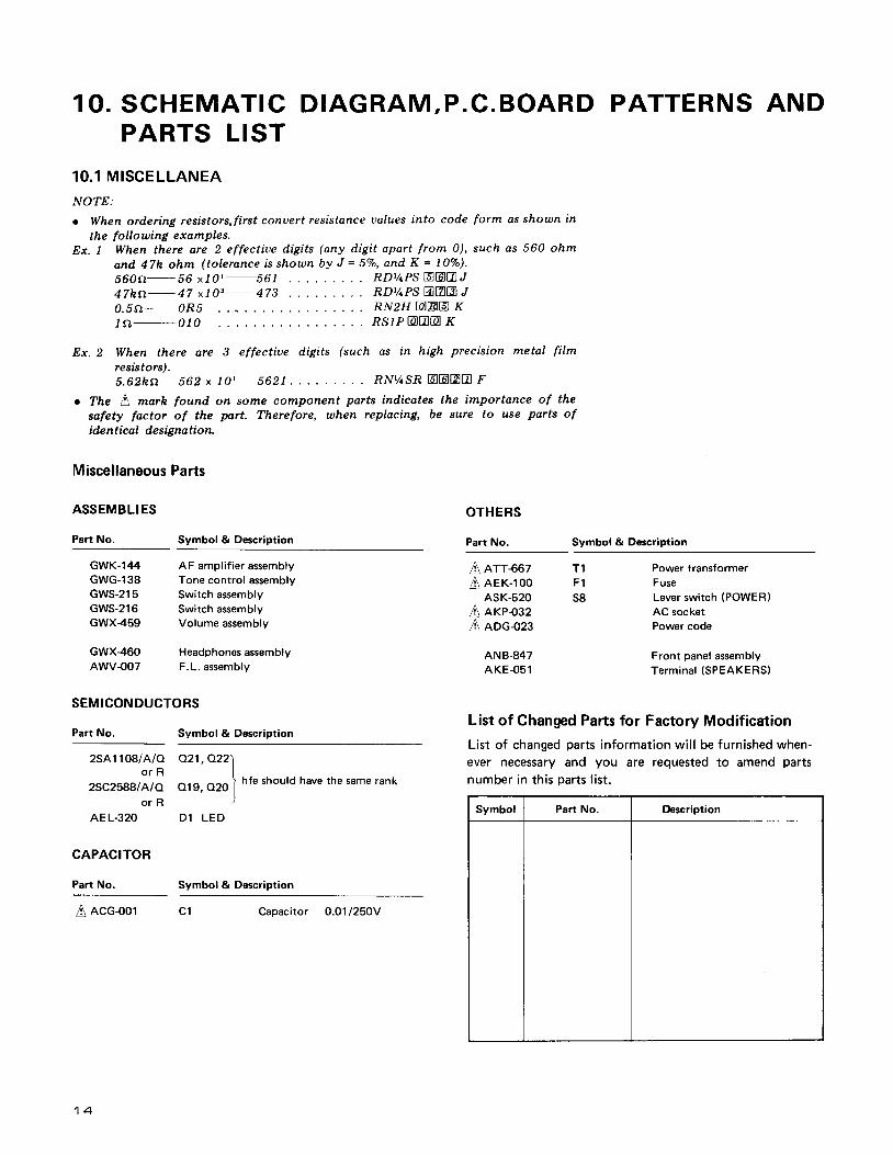
1O. SCHEMATIC DIAGRAM.P.C.BOARD PATTERNS ANDPARTS LIST
10.1 MISCELLANEA
NOTE:
c When ordering resistors,first conuert resistance ualues into code form as shown in
the following examples.Ex. 1 When there are 2 effectiue digits (any digit apart from 0), such as 560 ohm
and 47h ohm (tolerance is shown by J = SVo, and K = 10Vo).5 6 O a - 5 6 x 1 0 t - 5 6 1 . . . R D V T P S E @ I i l J4 7 h a - 4 7 x 1 0 3 - 4 7 3 . . . ' R D | / t P S A A B J6 . S a - 1 R S . . _ . . . R N 2 H @ E E Kt a - 0 1 0 . . . . . . 8 S r P @ [ 0 @ / (
Ex. 2 When there are 3 effective digits (such as in high precision metal filmresistors).5.62ha 562 x 10' 5621. . ' . RN7ISrB tr@gm ,F
o The A mark found on sotne component parts indicates the importance of thesafety factor of the part. Therefore, when replacing, be sure to use parts ofidentical designation.
Miscellaneous Parts
ASSEMBLIES
Part No. Symbol & Description
GWK-144 AF ampl i f ier assemblyGWG-138 Tone contro l assemblyGWS-215 Switch assemblyGWS-216 Switch assemblyGWX459 Volume assembly
GWX460 Headphones assemblyAWV-007 F.L. assembly
SEMICONDUCTORS
Part No. Symbol & Description
OTHERS
Part No. Symbol & Description
A 4TT-667 T1 Power transformer7\ ner-t oo F1 Fuse
ASK-520 SB Lever switch (POWER)
A nrpoez AC socketA nocozs
ANB-847A K E 4 5 1
Power code
Front panel assemblyTe rm ina l (SPEAKERS)
List of Changed Parts for Factory ModificationList of changed parts information wil l be furnished when-
2sA1108/A/o 021,422\ ever necessary and you are requested to amend parts
2sc2s88/i;5 019, o2o I nte snoura have the same rank number in this parts l ist.
o r R . j
AEL.32O D1 LED
CAPACITOR
Part No. Symbol & Description
A ACGOO1 C1 Capacitor 0.01/250V
Symbol Part No. Description
21 3
A
B
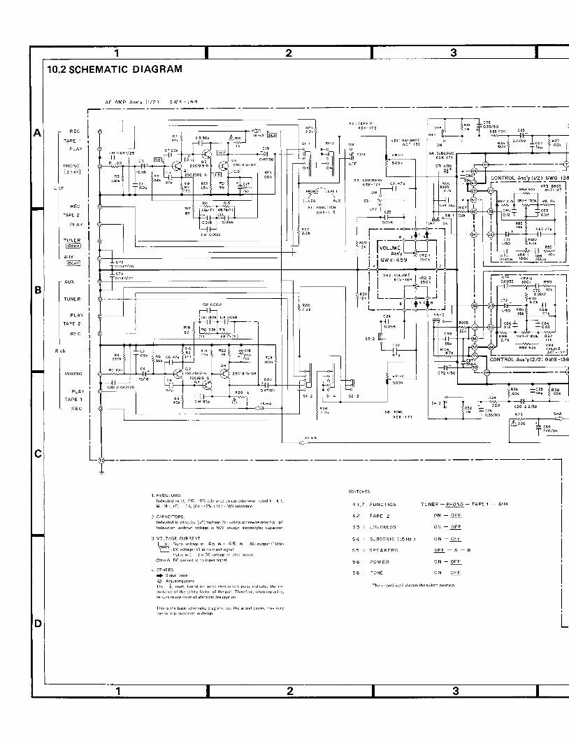
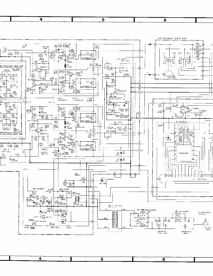
10.2 SCHEMATIC DIAGRAM
l - - - o t
o ' : o " t ' ' ( 1 / 2 ) G W - K - 1 4 4
f REc l s2: ' �aPEz-
[4Eg (
l:#i 'li-iI";+ II |IIp-]]*_|..."::.F':n I l_UI
l-r' i t---1 @ I I I l'"::'�""-#"I $"il | Lry Ii "'o" I E--l I H'l "'lffil {.i''#,,ffiffii
I t o o 4 7 / 2 5 r 3 l i 1 7 | |.AUX l J"'"1 i"*,'' 'rt5i illlF'-._'*i-'*ll:;; l 1\Jn*'ffiil-::: l{----l ::iHEi-Tf llll l _H ll. l ' l l l l l - - - . - . 1 f f iNrRoLAss.v(2 ,2 ,Gw6. ,3aI """-" i t*41+.t_|dr{::::,:^f{..",","u"1*,,oI | | Hl fd h| | l , JL-,=:i *HE-{
l^'- ftzzzu,l l r -Ll-- - rI
II
III
L
S W I T C H E S :
s t , 7 : F U N C T I O N T U N E R - P H O N O - T A P E I - A U X
S Z : T A p E ? O N - O F F
5 3 : L O U D N E S S O N - O F F
5 4 : S U B S O N I C ( 1 5 H z ) O N - O F F
5 5 : S P E A K E R S O F F - A - B
5 6 . P O W E R O N _ O F F
5 8 : T O N E O N - O F F
The under l ined ind ica tes the swi tch pos i t ion .
c
D
1 2 3
S W I T C H A s s ' y G W S - ? 1 5l - - _I
-lR 5 l2 . 2 k
D 3rs2075
c39o.ot/500
- ' - ^
f c67 27p Ii--T--i
; ??'?t I---"J"-l F ttr-J56
u'tt*' SB%,,
'o* lo.00r2
R r o l6 . 2 t
c 6 82 7 o
c t o t o k ! *l ' "l "F
nea'6zr YFl,i., I
_^.-J?rJ- - - d
) L A s s ' y ( 2 / 2 1 G W G - 1 3 8
I
8 2 0 ( t / 2 w )
I a s E - o o 3t-
2SC19r4A-G
ol 82P
ts2076
c6 l roo , /so Q 2 H A r 2 0 t O
*^^-J ,r.3i.R92 i lOk R52
R z O l g k R z Z t O C 4 8
az6 2scrass-R " ro A I o r r cezso
0 l ( P O W E R )
A I C 5 84A - O.Ol lACtso
T 2A T T - 5 7 7
ot7 l t /zwl
A r r o o i z s o
v r a A v - o o 6
A F A M P A s s ' y ( 2 / 2 1G W K - 1 4 4 A C P O W E R C O R O
a D G - o 2 3
AI cez ' 6 .o t t \L _ _ _ a c r 2 5 J
7 8 9
. - - -F- l .
__1__fr_I l l 3
i - 3 l ' . - . l L - Jr* J "Jl L_j| *r------ lll < # l l] l l n t - -
t t l
l l _ - - l - -
- -
-
-_l
d%&;+48?q-E
r l H l'/50 I+l
{ A t 2 0 t 0
=-----riE f l r l , ' lf l l l= l lm. li l l l* l l t t l . l-i s l l l ' l l l . l -
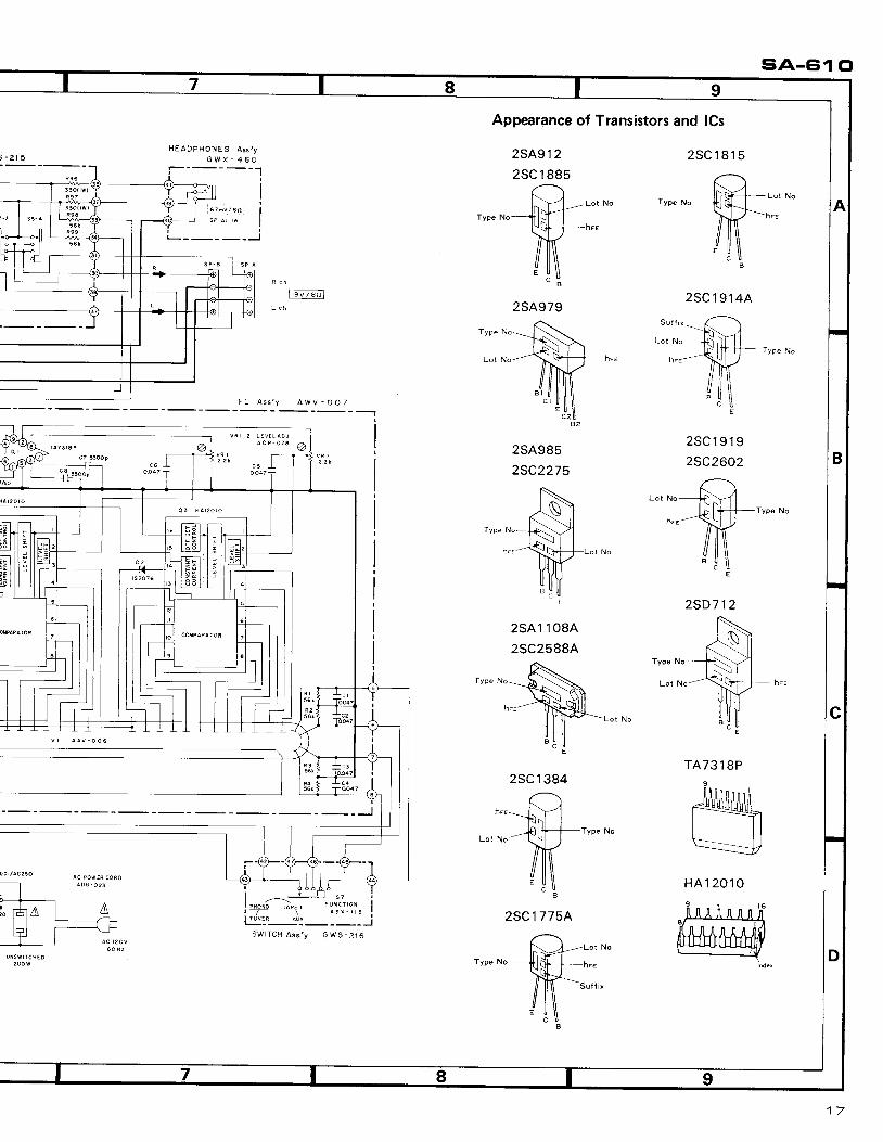
Appearance
2SA912
2SC 1 885
Orvpe..-fl${
) )a : u
2SA9 79-rype""$
u"tru"-*ffii-il"o 4[L\g_ l
IR ?
I
>'2k I
I- l il !l lt i
2SA985
2 S C 2 2 7 5
trr"-"$^"7
of Transistors and f Cs
2 S C 1 8 1 5
A
2 S C 1 9 1 4 4
suff ix===O
) ot No--B^
!ilf-rvpe No)-n'E h"-]1tt/
've
/ l \2SC '' n lg2SC 2602
,^\Lot No-S;a/
n*=-+*LfT-rvpe No
flKs ! \
B
3r!
2SA 1 1 08A
2SC2588A
Type *"-__N+\-\,\_\
n,.ffil l l t (J- --Lot
No
s u l lu s
2SC 1 38;
n"-$iir-ot ruo-{Ul+-rvpe
No
m/ ! \2sc , : : r^
? -- r ' � p-- . - -LotNo
rype ruo-{ t-hre
)fr1=--c,.{{i,i l
i l u surTrx
IE U \
2 S D 7 1 2
\fr'"ru"-fuLotNoff in' .
uu\iT A7'; ::
ru\--===-J
7 8 I
c
D
EiA-61cI
1 7
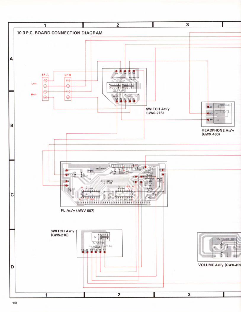
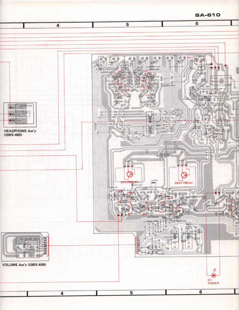
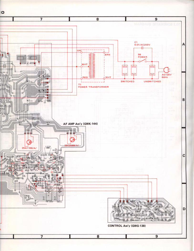
10.3 P.C. BOARD CONNECTION DIAGRAM
FL Asr'y (AWV.007I
Lch
R c h
HEADPHONE Arr'y(GWX460I
SWITCH As'y(cws-216)
EtA-Ci1 cl
HEADPHONE As'y(cwx460l
VOLUME Arr'y (GWX459)
2s�A11o,AlA/
Il o
ACl 20V6OHz
-t
;t
*L - - - - - - _ - - _ J
T 1POWER TF IANSFORMER
S W I T C H E O U N S W I T C H E O
AF AMP Ar'y (GWK-1441
CONTROL Ar'y (GWG-I38)
siA-61 Cl
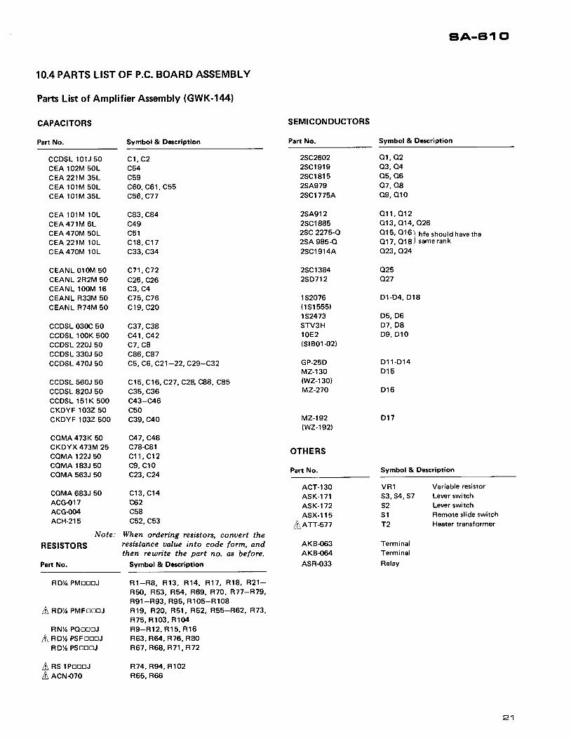
10.4 PARTS LIST OF P.C. BOARD ASSEMBLY
Parts List of Amplifier Assembly (GWK-144)
CAPACITORS
Part No. Symbol & Description
SEMICONDUCTORS
Part No. Symbol & Description
ccDsL 101J 50CEA 1O2M sOLCEA 221M 35LC E A 1 O l M s O LC E A 1 0 1 M 3 5 L
C E A 1 0 1 M 1 O LC E A 4 7 1 M 6 LCEA 47OM sOLC E A 2 2 1 M 1 O LC E A 4 T O M 1 O L
CEANL OlOM 50CEANL 2R2M 50CEANL lOOM 16CEANL R33M 50CEANL R74M 50
ccDsl mrc 50ccDSL 100K 500ccDSL 220J 50ccDSL 330J 50ccDSL 470J 50
ccDsL 560J 50ccDSL 820J 50ccDSL 151K 500CKDYF 1032 50cKDYF 1032 500
coMA 473K 50CKDYX 473M 25coMA 122J 50coMA 183J 50coMA 563J 50
coMA 683J 50ACG-017ACG-004ACH-215
Note:
RESISTORS
Part No.
25C26022SC1 91 92SC1 81 525A97925C17754
2SA91 22SC18852SC 2275-02SA 985-O2SC1 91 4A
2SC138425D712
1 S2076( 1 S1 555)152473STV3H10F-2(s rBo1-02)
GP-25DMZ-130{wz-130}MZ-270
MZ- I92lwz-l921
OTHERS
Part No.
01, 0203, 0405, 0607, 0809, 010
01 I , 012013, 014, 026015, 016 l h fe shoutdhavethe01 7, 01 8 J same ran ko23,O24
o2so27
Dl-D4, D l8
D5, D6D7, D8D9, D lO
D 1 1 - D 1 4D l 5
D 1 6
D17
c ' t , c2c54c59c60, c61, cssc56,C77
c83, C84c49c51c 1 8 , C 1 7c33, C34
c71,c72c25, C26c3, c4c75, C76c19, C20
c37, C38c41, C42c 7 , c 8c86, C87c5, c6 , c21-22,C29-C32
c15, C16, C27,C2A, C88, C85c35, C36c43-C46c50c39, C40
c47, C48c78-C81c11, C12c9, cl0c23, C24
c 1 3 , C l 4c62c58c52, C53
When ordering resistors, convert theresistance ualue into code form, andthen rewrite the part no, as before.
Symbol & Description
Symbol & Description
ACT-130ASK-1 71ASK-172ASX. I 15
Inrr-szz
AKB.063AK8-064ASR-033
V R 1s3, s4, s7s2s 1T2
TerminalTerminal
Relay
Variable resistor
Lever switchLever switchRemote s l ide swi tchHeater transformer
RD!/r PMoDtrJ
A noy. PMFoooJ
RNTc POootrJARD% PsFotroJ
RD% PSOOOJ
A RS t poool
A ncruozo
R 1 - R 8 . R 1 3 , R 1 4 , R 1 7 , R 1 8 , R 2 1 -R50, R53, R54, R69, R70, R77-R79,R91-R93, R95, R105-R108R19, R20, R51, R52, R55-R62. R73,R75, R103, R l04B g - R 1 2 , R 1 5 , R 1 6R63, R64, R76, R80R67, R68, R71,R72
R74, R94, R102R65, R66
2 1
Parts List of Tone Control Assembly (GWG-I3b) Parts List of Switch Assembly (GWS-216)
CAPACITORS
Part No. Symbol & Description
c63, C64c65, C66c67, C68c69, C70c73, C74
When ordering resistors, conuert theresistance ualue into code form, andthen rewrite the part no. as before.
Symbol & Description
VR3. VR4 Variable resistorR 8 1 - R 9 0 , R 1 0 1 , R 1 0 0
Assembly (cWS-215)
Symbol & Description
Part No. Symbol & Description
ASX-1 |3 56 Sl ide rotary swi tch (FUNCTION)
Parts List of Volume Assembly (GWX-4S9)
Part No. Symbol & Description
ACV-184 VR2 Var iable resistor (VOLUME)
Parts List of Headphones Assembly (GWX-460)
Part No. Symbol & Description
AKN-023 Headphones jack
coMA 303J 50coMA 124K 50cosA 270K sOCQMA 122K 50coMA 562K 50
Note:
RESISTORS
Part No.
ACT-127RDT4PMD tr qJ
Parts List of Switch
Part No.
ASE.OO3R S l P 3 3 1 JRDlzrPM 563J
55 Slide rotary switch (SPEAKERS)R96, R97R98, R99
Description
0
I
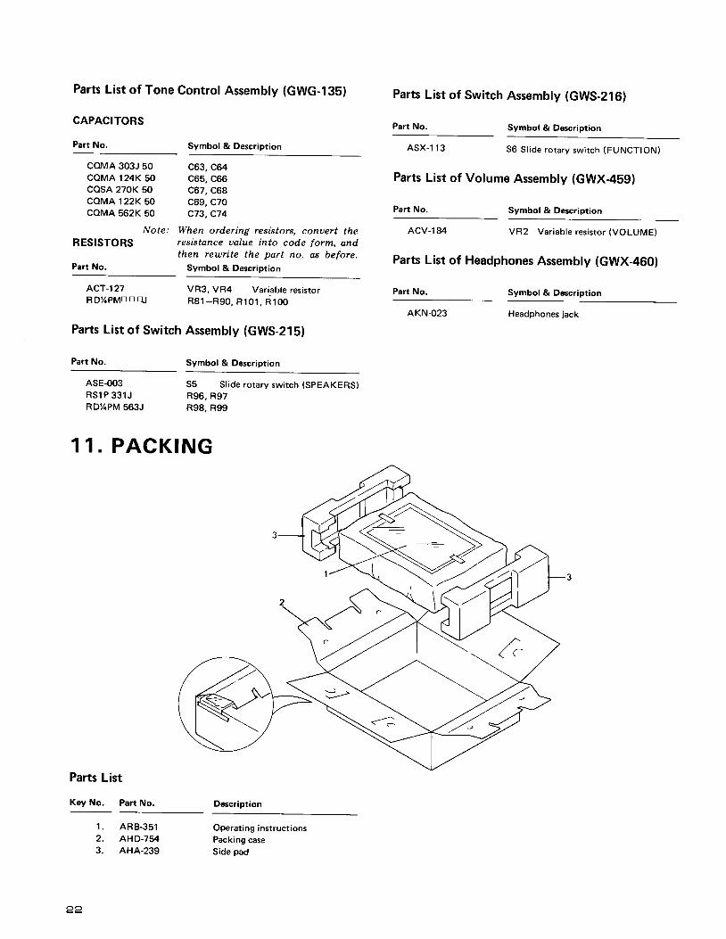
1 1 . P A C K I N G
Parts List
Key No. Part No.
1 .2 .3 .
ARB.351AHD.754AH4.239
Operat ing instruct ionsPacking caseSide pad

)a
PICINEEFI ELECTFICINIC CCIFIPCIFIATICIN 4-1, Mesuno 1-chome, Mesuno-ku. Tokyo 'l 53, JapenU.a. FEIfVEEFI EI-ECTFICDNICE CCIFIPCIF|ATICIN E|5 Oxfond Dnive, Moon€chie, New Jereey O7O7\ U.S.A.FGIilCEFI eECTFlClillC (El.rFlCtFE N.\/. Luithagen-Heven 9,2O3O Antwe.p, ElelgiumFCIwCEF El-CTFlCtI\llC|l A|J3TFIALIA FTY. LtEl. 17A-1A4 Eloundenv F|oad. Eltreeside. Victonia 3'l 95, Augtnelie
(aRT '478€) E A i T - . a 7 q P F h t e d i n J e o a n