Embed Size (px)
Citation preview

FN2808Rev 12.00
July 27, 2009
HSP43168Dual FIR Filter
DATASHEETNOT RECOMMENDED FOR NEW DESIGNS
NO RECOMMENDED REPLACEMENT
contact our Technical Support Center at
1-888-INTERSIL or www.intersil.com/tsc
The HSP43168 Dual FIR Filter consists of two independent 8-tap FIR filters. Each filter supports decimation from 1 to 16 and provides on-board storage for 32 sets of coefficients. The Block Diagram shows two FIR cells each fed by a separate coefficient bank and one of two separate inputs. The outputs of the FIR cells are either summed or multiplexed by the MUX/Adder. The compute power in the FIR Cells can be configured to provide quadrature filtering, complex filtering, 2-D convolution, 1-D/2-D correlations, and interpolating/decimating filters.
The FIR cells take advantage of symmetry in FIR coefficients by pre-adding data samples prior to multiplication. This allows an 8-tap FIR to be implemented using only 4 multipliers per filter cell. These cells can be configured as either a single 16-tap FIR filter or dual 8-tap FIR filters. Asymmetric filtering is also supported.
Decimation of up to 16 is provided to boost the effective number of filter taps from 2 to 16 times. Further, the Decimation Registers provide the delay necessary for fractional data conversion and 2-D filtering with kernels to 16x16.
The flexibility of the Dual is further enhanced by 32 sets of user programmable coefficients. Coefficient selection may be changed asynchronously from clock to clock. The ability to toggle between coefficient sets further simplifies applications such as polyphase or adaptive filtering.
The HSP43168 is a low power fully static design implemented in an advanced CMOS process. The configuration of the device is controlled through a standard microprocessor interface.
Features
• Two Independent 8-Tap FIR Filters Configurable as a Single 16-Tap FIR
• 10-Bit Data and Coefficients
• On-Board Storage for 32 Programmable Coefficient Sets
• Up To: 256 FIR Taps, 16x16 2-D Kernels, or 10x19-Bit Data and Coefficients
• Programmable Decimation to 16
• Programmable Rounding on Output
• Standard Microprocessor Interface
• Pb-Free Available (RoHS Compliant)
Applications
• Quadrature, Complex Filtering
• Image Processing
• Polyphase Filtering
• Adaptive Filtering
Ordering Information
PART NUMBER PART MARKINGTEMP. RANGE
(°C) PACKAGEPKG.
DWG. #
HSP43168VC-45 HSP43168VC-45 0 to +70 100 Ld MQFP Q100.14x20
HSP43168VC-45Z (Note) HSP43168VC-45Z 0 to +70 100 Ld MQFP (Pb-free) Q100.14x20
HSP43168JC-33 HSP43168JC-33 0 to +70 84 Ld PLCC N84.1.15
HSP43168JC-33Z (Note) HSP43168JC-33Z 0 to +70 84 Ld PLCC N84.1.15
NOTE: These Intersil Pb-free plastic packaged products employ special Pb-free material sets, molding compounds/die attach materials, and 100% matte tin plate plus anneal (e3 termination finish, which is RoHS compliant and compatible with both SnPb and Pb-free soldering operations). Intersil Pb-free products are MSL classified at Pb-free peak reflow temperatures that meet or exceed the Pb-free requirements of IPC/JEDEC J STD-020.
FN2808 Rev 12.00 Page 1 of 25July 27, 2009

HSP43168
Block Diagram
Pinouts HSP43168
(84 LD PLCC)TOP VIEW
FIR CELL A
COEFFICIENTBANK A
CIN0 - 9A0 - 8
WR
INA0 - 9
OUT9 - 27
CONTROL/CONFIGURATION
MUX /ADDER
10
9 19
INB0 - 9/OUT0 - 8
OEHOEL
CSEL0 - 4
MUX
MUX FIR CELL B
COEFFICIENTBANK B
10
10
9
666768697071727374
5859606162636465
54555657
201918171615141312
2827262524232221
32
31
3029
INB
2IN
B 3
INB
4
INB
5IN
B 6
INB
8IN
B 7
GN
D
OU
T 1
3O
UT
12
OU
T 1
1
OU
T 9
INB
1IN
B 0
OU
T 1
0V
CC
OU
T 1
4O
UT
15
GN
D
OU
T 1
6
OE
L
RVRSFWD
TXFR
OUT 27OUT 26OUT 25OUT 24OUT 23OUT 22OUT 21OUT 20OUT 19
OUT 17VCC
VCC
OEHGND
ACCEN
CLK
OUT 18
SHFTENCIN 6
CIN 2
INA 9
INA 7INA 6INA 5
INA 3
CIN 7
CIN 4GND
CIN 3
CIN 0
VCC
INA 2INA 1INA 0INB 9
CIN 5
CIN 1
INA 8
INA 4
33 34 35 36 37 38 39 40 41 42 43 44 45 46 47 48 49 50 51 52 53
11 10 9 8 7 6 5 4 3 2 1 84 83 82 81 80 79 767778 75
A 4
A 6
A 7
CS
EL
3
A 5
A 3
A 0
CS
EL
4C
IN 9
A 2
CIN
8
CS
EL
1
CS
EL
0
A 8
A 1
GN
D
MU
X 1
MU
X 0
CS
EL
2
VC
C
WR
FN2808 Rev 12.00 Page 2 of 25July 27, 2009

HSP43168
HSP43168(100 LD MQFP)
TOP VIEW
Pinouts (Continued)
99 98 97 96 95 94 93 91 89 87 85 84 83 818286889092100
7980
78777675747372717069686766656463626160595857565554535251
21
3456789101112131415161718192021222324252627282930
32 33 34 35 36 37 38 40 42 44 46 47 48 50494543413931
WR
VC
C
VC
C
CIN
9
GN
D
GN
D
A0
A1
A2
A3
A4
A5
A6
A7
A8
CS
EL
0
CS
EL
1
CS
EL
2
CS
EL
3
CS
EL
4
INA5
CIN0INA9INA8INA7INA6
VCCVCC
INA4INA3
CIN1
INA1INA0
INA2
NCCIN7
NCCIN6CIN5
GNDCIN4
GNDCIN3CIN2
CIN8
NCNC
INB7
INB9INB8
OUT18OUT17NCVCC
GNDGND
VCC
OUT19
GNDOEHOUT27OUT26
OUT24OUT23OUT22OUT21OUT20
OUT25
GND
MUX0RVRSNCFWRD
TXFRACCENVCCVCCCLK
SHIFTEN
MUX1
INB
6
GN
DG
ND
INB
5
INB
4IN
B3
INB
2IN
B1
INB
0O
EL
OU
T9
OU
T1
0V
CC
VC
CO
UT
11O
UT
12
OU
T1
3O
UT
14
OU
T1
5O
UT
16
FN2808 Rev 12.00 Page 3 of 25July 27, 2009

HSP43168
Pin Description
SYMBOL TYPE DESCRIPTION
VCC VCC: +5V power supply pin
GND Ground
CIN0-9 I Control/Coefficient Data Bus. Processor interface for loading control data and coefficients. CIN0 is the LSB
A0-8 I Control/Coefficient Address Bus. Processor interface for addressing Control and Coefficient Registers. A0 is the LSB
WR I Control/Coefficient Write Clock. Data is latched into the Control and Coefficient Registers on the rising edge of WR
CSEL0-4 I Coefficient Select. This input determines which of the 32 coefficient sets are to be used by FIR A and B. This input is registered and CSEL0 is the LSB.
INA0-9 I Input to FIR A. INA0 is the LSB
INB0-9 I/O Bidirectional Input for FIR B. INB0 is the LSB and is input only. When used as output, INB1-9 are the LSBs of the output bus, and INB9 is the MSB of these bits.
OUT9-27 O 19 MSBs of Output Bus. Data format is either unsigned or two's complement depending on configuration. OUT27 is the MSB.
SHFTEN I Shift Enable. This active low input enables clocking of data into the part and shifting of data through the Decimation Registers.
FWRDFWD
I Forward ALU Input Enable. When active low, data from the forward decimation path is input to the ALUs through the “a” input. When high, the “a” inputs to the ALUs are zeroed.
RVRS I Reverse ALU Input Enable. When active low, data from the reverse decimation path is input to the ALUs through the “b” input. When high, the “b” inputs to the ALUs are zeroed.
TXFR I Data Transfer Control. This active low input switches the LIFO being read into the reverse decimation path with the LIFO being written from the forward decimation path (see Figure 1).
MUX0-1 I Adder/Mux Control. This input controls data flow through the output Adder/Mux. Table 5 lists the various configurations.
CLK I Clock. All inputs except those associated with the processor interface (CIN0-9, A0-8, WR) and the output enables (OEL, OEH) are registered by the rising edge of CLK.
OEL I Output Enable Low. This three-state control enables the LSBs of the output bus to INB1-9 when OEL is low.
OEH I Output Enable High. This three-state control enables OUT9-27 when OEH is low.
ACCEN I Accumulate Enable. This active high input allows accumulation in the FIR Cell Accumulator. A low on this input latches the FIR Accumulator contents into the Output Holding Registers while zeroing the feedback pass in the Accumulator.
NC No connect
FN2808 Rev 12.00 Page 4 of 25July 27, 2009

FN
280
8R
ev 1
2.00P
age 5 of 2
5July 27, 2009
HS
P4
31
68
DELAY1-16 ††
ALUA B
LIFO A
LIFO B
DELAY1-16
MUX
MUX
DEMUX
DELAY1-16 ††
COEFBANK
REG
XCOEFBANK
REG
OUT9-27
†ODD/EVEN
†ODD/EVEN
FIR CELL B
DATA FEEDBACK CIRCUITRY
PUTDINGISTER
32
NUMBER OF
† Processor control words
FIR B REVERSE PATH
FIR B FORWARD PATH
SYMMETRY
†FIR B
ODD/EVEN # TAPS
†DATA REVERSAL ENABLE
†† Decimation factor
TAPS
DELAY1-16 ††
DELAY1-16 ††DELAY 3
ALUA B
ALUA B
ALUA B
ALUA B
INA0-9
INB1-9/
LIFO A
LIFO B
DELAY1-16 ††
MUX
MUX
DEMUX
MUX
MUX
DELAY1-16 ††
DELAY1-16 ††
DELAY1-16 ††
DELAY1-16 ††
DELAY1-16 ††
DELAY1-16 ††
ALUA B
ALUA B
ALUA B
DELAY 3
DELAY 4 MUXDELAY 3
DELAY 3
DELAY 3
REG
X COEFBANK
REG
REG
X COEFBANK
REG
REG
X
REG
REG
X COEFBANK
REG
REG
XCOEFBANK
REG
REG
XCOEFBANK
REG
REG
X
REG
DELAY 4
ADDERMUX
REG
0
DELAY 5
MUX/ADDER
DELAY 2CONTROL
DELAY 6
OEL
OEH
A0-8
WR
MUX0-1
ACCEN
CIN0-9
CSEL0-4
FWRD
RVRS
SHFTEN
TXFR
†ODD/EVEN
†MODE SELECT
†MODE SELECT
FIR CELL A
10
9
10
5
9
2
199
†ROUND ENABLE
OUT0-8
INB0
REG
ADDERMUX
REG
0REG
FIR AACCUMULATOR
FIR BACCUMULATOR
DATA FEEDBACK CIRCUITRY
OUTHOLREG
OUTPUTHOLDINGREGISTER
DECIMATION REGISTERS DECIMATION REGISTERS
3210 10
DELAY1-16 ††
DELAY1-16 ††
DELAY1-16 ††
DELAY 3
DELAY 4 MUXDELAY 3
FIGURE 1. DUAL FIR FILTER
COEFBANK
†ODD EVEN SYMMETRY†FIR A ODD/EVEN # TAPS†FIR B ODD/EVEN # TAPS†FIR B INPUT SOURCE†DATA REVERSAL ENABLE†ROUND ENABLE†DECIMATION FACTOR
†FIR B INPUTSOURCE
SYMMETRY
†FIR A ODD/EVEN # TAPSFIR A REVERSE PATH
FIR A FORWARD PATH
†ODD/EVEN SYMMETRY
†MODE SELECT
†DATA REVERSAL ENABLE
28
11
10
21
11
1010
22
CLK
1
0
1
0

HSP43168
Functional DescriptionAs shown in Figure 1, the HSP43168 consists of two 4-multiplier FIR filter cells which process 10-bit data and coefficients. The FIR cells can operate as two independent 8-tap FIR filters or two 4-tap asymmetric filters at maximum I/O rates. A single filter mode is provided which allows the FIR cells to operate as one 16-tap FIR filter or one 8-tap asymmetric filter. On board coefficient storage for up to 32 sets of 8 coefficients is provided. The coefficient sets are user selectable and are programmed through a microprocessor interface. Programmable decimation to 16 is also provided. By utilizing Decimation Registers together with the coefficient sets, polyphase filters are realizable which allow the user to trade data rate for filter taps. The MUX/Adder can be configured to either add or multiplex the outputs of the filter cells depending upon whether the cells are operating in single or dual filter mode. In addition, a shifter in the MUX/Adder is provided for implementation of filters with 10-bit data and 20-bit coefficients or vice versa.
Preparing the Dual FIR for OperationTwo configuration steps are required to prepare the Dual FIR Filter for normal operation: 1) loading the Configuration Control Registers, and 2) loading the FIR Filter Coefficients.
Configuration Control Registers are loaded by placing the control register address on address lines A0-8, placing the configuration data on the configuration input lines CIN0-9, and asserting the WR line (followed by a release of the assertion). This action creates a rising edge on the WR line, which clocks the address and configuration data into the part. The details of the “Load Configuration” process are outlined in “Microprocessor Interface” on page 6.
FIR Coefficients are loaded by placing the address of the Coefficient Data Bank on the address lines A0-8, placing the FIR 10-bit coefficient values on the configuration input lines CIN0-9 and then asserting the WR line (followed by a release of the assertion). This action creates a rising edge on the WR line, which clocks the FIR Coefficient Band address and FIR Coefficient data into the part. The details of the “Load FIR Coefficient” process are outlined in “Coefficient Bank” on page 8.
Both the Configuration Load and FIR Coefficient Load can be done as a sequence of asynchronous write commands to the Dual FIR Filter. Once these actions are complete, the part is ready for normal filter operation. The CLK, TXFR, FWRD, RVRS, ACCEN, and SHFTEN signals must be asserted in a manner determined by the application. MUX0-1 must meet the setup and hold times with respect to clock for proper filter operation. Details of the MUX1-0 control can be found in “Output MUX/Adder” on page 9. Details of the ACCEN control can be found in “FIR Cell Accumulator” on page 9. Bit locations for the various filter control/configuration signals can be found in “Input/Output Formats” on page 10.
The Dual FIR Filter has a “pipeline” delay of 8 CLK periods, once normal filtering operations begin. Five typical filtering operation examples are provided in “Application Examples” on page 10 as a guide to configuration and control of the Dual FIR Filter.
During normal filter operations, the location and duration of the TXFR signal assertions are determined by the filter configuration and operation mode. Once set, these signal parameters must be maintained during normal operation to ensure proper data alignment in the part. Once the part is reset, do not change TXFR unless you load the configuration again.
Note: The fixed or periodic relationship between the TXFR signal and CLK must be maintained for valid filter operation. This relationship can only change when CLK is halted and new configuration control words are loaded into the device.
Microprocessor InterfaceThe Dual FIR has a 20 pin write only microprocessor interface for loading data into the Control Block and Coefficient Banks. The interface consists of a 10-bit data bus (CIN0-9), a 9-bit address bus (A0-8), and a write input (WR) to latch the data into the on-board registers on a rising edge. The configuration control and coefficient data loading is asynchronous to CLK.
Control BlockThe Dual FIR is configured by writing to the registers within the Control Block. Figure 2 shows the timing diagram for writing to the Configuration Control Registers. These Control Registers are memory mapped to Address 000H (H = Hexadecimal) and 001H on A0-8. The Filter Coefficient Registers are mapped to 1XXH (X = value described in “Coefficient Bank” on page 8).
The format of the Control Registers is shown in Table 1 and Table 2. Writing to any of the Control/Configuration Registers causes a reset which lasts for 6 CLK cycles following the assertion of WR. The reset caused by Writing Registers in the Control Block will not clear the contents of the Coefficient Bank. As shown in Figure 2, either Configuration Control Register can be written to during reset.
WR
A8-0
C9-0
000H
FIGURE 2. LATCHING C9-0 VALUES INTO ADDRESS A8-0 REGISTERS
RESET
001H
FN2808 Rev 12.00 Page 6 of 25July 27, 2009

HSP43168
The 4 LSBs of the control word loaded at address 000H are used to select the decimation factor. The Decimation Factor is programmed to one less than the number of delays between filter taps as shown in Equation 1.
For example, if the 4 LSBs are programmed with a value of 0010, the Forward and Reverse Shifting Decimation Registers are each configured with a delay of 3. Bit 4 is used to select whether the FIR cells operate as two independent filters or one extended length filter. Dual filter mode assumes Filter A and Filter B are separate independent filters. In the single filter mode, the data is routed through the forward paths of Filters A and B before entering the reverse paths of Filters A and B
(see Figure 1). Coefficient symmetry is selected by bit 5. Bits 6 and 7 are programmed to configure the FIR cells for odd or even filter lengths (number of taps). Bit 8 selects the FIR B input source when the FIR cells are configured for independent operation. Bit 9 must be programmed to 0. Note: When the filter is programmed for even-taps, the TXFR signal is delayed by only three CLKS (see Figure 1). For odd-taps, the TXFR signal is delayed by four CLKS.
The 4 LSBs of the control word loaded at address 001H are used to configure the format of the FIR cell's data and coefficients. Bit 4 is programmed to enable or disable the reversal of data sample order prior to entering the Reverse Path Decimation Registers. Data reversal is required for symmetric filter coefficient sets of both even or odd numbers of filter taps. Asymmetric filters and some decimated symmetric filters require the data reversal to be off. Bits 5 to 9 are used to support programmable rounding on the output.
FIR Filter CellsEach FIR filter cell is based on an array of four 11x10-bit two's complement multipliers. One input of the multipliers comes from the ALU’s which combine data shifting through the Forward and Reverse Decimation Registers. The second multiplier input comes from the user programmable coefficient bank. The multiplier outputs are fed to an accumulator whose result is passed to the output section where it is multiplexed or added with the result from the other FIR cell.
Decimation Registers
The Forward and Reverse Decimation Shift Registers can be configured for decimation factors from 1 to 16 (see Table 1, bits 0-3). Note: Setting the decimation factor only affects the Delay Registers between filter taps, not the filter control multiplexers. Example 4 and Example 5 in “Application Examples” on page 10 discuss how to configure the part for actual decimation applications.
The Reverse Shifting Registers with the data reversal logic are used to take advantage of symmetry in linear phase filters by aligning data at the ALUs for pre-addition prior to multiplication by the common coefficient. When the FIR cells are configured in single filter mode, the Decimation Registers in FIR cell A and FIR cell B are cascaded. This extended filter tap delay path allows computation of a filter which is twice the size of that capable using a single cell. The Decimation Registers also provide data storage for polyphase or 2-D filtering applications (See “Application Examples” on page 10).
The Data Feedback Circuitry in each FIR cell is responsible for transferring data from the Forward to the Reverse Shifting Decimation Registers. This circuitry feeds blocks of samples into the reverse shifting decimation path in either reversed or non-reversed sample order. The MUX/DEMUX structure at the input to the Feedback Circuitry routes data to the LIFOs or the delay stage depending on the selected
TABLE 1. CONFIGURATION/CONTROL WORD 0 BIT DEFINITIONS
CONTROL ADDRESS 000H
BITS FUNCTION DESCRIPTION
3-0 Decimation Factor (N) R = N + 10000 = No Decimation.1111 = Decimation by 16.
4 Mode Select 0 = Single Filter Mode.1 = Dual Filter Mode.(also 20-Bit Coefficient Filter)
5 Odd/Even Filter Coefficient Symmetry
0 = Even Symmetric Coefficients.1 = Odd Symmetric Coefficients.
6 FIR A Odd/Even Number of Taps
0 = Odd Number of Taps in Filter.1 = Even Number of Taps in Filter.
7 FIR B Odd/Even Number of Taps
(Defined Same as FIR A Above).
8 FIR B Input Source 0 = Input from INA0-9.1 = Input from INB0-9.
9 Not Used Set to 0 for Proper Operation.
TABLE 2. CONFIGURATION/CONTROL WORD 1 BIT DEFINITIONS
CONTROL ADDRESS 001H
BITS FUNCTION DESCRIPTION
0 FIR A Input Format 0 = Unsigned.1 = Two's Complement.
1 FIR A Coefficient Format (Defined same as FIR A input).
2 FIR B Input Format (Defined same as FIR A input).
3 FIR B Coefficient (Defined same as FIR A input).
4 Data Reversal Enable 0 = Enabled.1 = Disabled.
8-5 Round Position 0000 = 2-10.
1011 = 21.
(See Figure 4)
9 Round Enable 0 = Enabled.1 = Disabled.
NOTES:
1. Address locations 002H to 011H are reserved, and writing to these locations will have unpredictable effects on part configuration.
DF CLK delays between taps 1–= (EQ. 1)
FN2808 Rev 12.00 Page 7 of 25July 27, 2009

HSP43168
configuration. The MUX on the Feedback Circuitry Output selects which storage element feeds the Reverse Shifting Decimation Registers.
In applications requiring reversal of sample order, the FIR cells are configured with data reversal enabled (see Table 2, CW5, bit 4 = 0). In this mode, data is transferred from the forward to the backward Shifting Registers through a pingponged LIFO structure. While one LIFO is being read into the backward shifting path, the other LIFO is written with data samples. The MUX/DEMUX controls which LIFO is being written, and the MUX on the Feedback Circuitry output controls which LIFO is being read. A low on TXFR and SHIFTEN, switches the LIFOs being read and written, which causes the block of data to be read from the structure in reversed in sample order (See Example 4 in “Application Examples” on page 10).
The frequency with which TXFR is asserted determines size of the data blocks in which sample order is reversed. For example, if TXFR is asserted once every three CLKs, blocks of 3 data samples with order reversed, would be fed into the Backward Decimation Registers. Note: Altering the frequency or phase of TXFR assertion once a filtering operation has begun will invalidate the filtering result.
In applications which do not require sample order reversal, the FIR cells must be configured with data reversal disabled (see Table 2, CW5, Bit 4 = 1). In addition, TXFR must be asserted to ensure proper data flow. In this configuration, data to the backward shifting decimation path is routed though a delay stage instead of the pingpong LIFOs. The number of registers in the delay stage is based on the programmed decimation factor. Note: Data reversal must be disabled and TXFR must be asserted for filtering applications which do not use decimation.
The shifting of data through the Forward and Reverse Decimation Registers is enabled by asserting the SHFTEN input. When SHFTEN is high, data shifting is disabled, and the data sample latched into the part on the previous clock is the last input to the filter structure. The data sample at the filter input when SHFTEN is asserted, will be the next data sample into the forward decimation path.
When operating the FIR cells as two independent filters, FIR A receives input data via INA0-9 and FIR B receives data from either INA0-9 or INB0-9 depending on the application (see Table 1).
When the FIR cells are configured as a single extended length filter, the forward and reverse decimation paths of the two FIR cells are cascaded. In this mode, data is transferred from the forward decimation path to the reverse decimation path by the Data Feedback Circuitry in FIR B. Thus, the manner in which data is read into the reverse decimation path is determined by FIR B's configuration. When the decimation paths are cascaded, data is routed through the fourth delay stage in FIR A's forward path to FIR B.
The configuration of the FIR cells as even or odd length filters determines the point in the forward decimation path from which data is multiplexed to the Data Feedback Circuitry. For example, if the FIR cell is configured as an odd length filter, data prior to the last register in the third forward decimation stage is routed to the Feedback Circuitry. If the FIR cell is configured as an even length filter, data output from the third forward decimation stage is multiplexed to the Feedback Circuitry. This is required to ensure proper data alignment with symmetric filter coefficients (See “Application Examples” on page 10).
ALUsData shifting through the forward and reverse decimation paths feed the “a” and “b” inputs of the ALUs respectively. The ALUs perform an “b+a” operation if the FIR cell is configured for even symmetric coefficients or an “b-a” operation if configured for odd symmetric coefficients. Control Word 0, Bit 5 is used to set the ALU operation.
For applications in which a pre-add or subtract is not required, the “a” or “b” input can be zeroed by disabling FWRD or RVRS respectively. This has the effect of producing an ALU output which is either “a”, “-a”, or “b” depending on the filter symmetry chosen. For example, if the FIR cell is configured for an even symmetric filter with FWRD low and RVRS high, the data shifting through the Forward Decimation Registers would appear on the ALU output.
Table 3 details the ALU configurations, where “a” is the ALU data input from the front decimation delay registers and “b” is the ALU data from the back decimation delay registers.
Coefficient Bank
The output of the ALU is multiplied by a coefficient from one of 32 user programmable coefficient sets. Each set consists of 8 coefficients (4 coefficients for FIR A and 4 for FIR B). CSEL0-4 is used to select a coefficient set to be used. Coefficient sets may be switched every clock to support polyphase filtering operations.
TABLE 3. ALU CONFIGURATIONS
ALU OUT SYMMETRY FWD RVS DESCRIPTION
a+b 0 (Even) 0 0 Even Number of Taps, Even Symmetry (Example 1)
+b 0 (Even) 0 1 Even Symmetry
+a 0 (Even) 1 0 Even Symmetry
- 0 (Even) 1 1 Even Symmetry
b-a 1 (Odd) 0 0 Even Number of Taps, Odd Symmetry (Example 2)
+b 1 (Odd) 0 1 Odd Symmetry
-a 1 (Odd) 1 0 Odd Symmetry
- 1 (Odd) 1 1 Odd Symmetry
FN2808 Rev 12.00 Page 8 of 25July 27, 2009

HSP43168
The coefficients are loaded into On-Board Registers using the microprocessor interface, CIN0-9, A0-8, and WR. Each multiplier within the FIR Cells is driven by a coefficient bank with one of 32 coefficients. These coefficients are addressed as shown in Table 4. The inputs A0-1 specify the Coefficient Bank for one of the four multipliers in each FIR Cell; A2 specifies FIR Cell A or B; Bits A7-3 specify one of 32 sets in which the coefficient is to be stored. For example, an address of 10dH would access the coefficient for the second multiplier in FIR B in the second coefficient set.
FIR Cell AccumulatorThe registered outputs from the multipliers in each FIR cell feed an accumulator. The ACCEN input controls each accumulator's running sum and the latching of data from the accumulator into the Output Holding Registers. When ACCEN is low, feedback from the accumulator adder is zeroed which disables accumulation. Also, output from the accumulator is latched into the Output Holding Registers. When ACCEN is asserted, accumulation is enabled and the contents of the Output Holding Registers remain unchanged.
Output MUX/AdderThe contents of each FIR Cell's Output Holding Register is summed or multiplexed in the Mux/Adder. The operation of the Mux/Adder is controlled by the MUX1-0 inputs as shown in Table 5. Applications requiring 10-bit data and 20-bit coefficients or 20-bit data and 10-bit coefficients are made possible by configuring the MUX/Adder to scale FIR B's output by 2-10 prior to summing with FIR A. When the Dual FIR is configured as two independent filters, the MUX1-0 inputs would be used to multiplex the filter outputs of each cell. For applications in which FIR A and B are configured as a single filter, the MUX/Adder is configured to sum the output of each FIR cell.
NOTE: While a 20-bit coefficient filter is a single filter, the mode select is set to 1 and MUX1-0 is set to 00.
TABLE 4. FIR COEFFICIENT WRITE ADDRESSES
FIRCOEFF.
CSEL (4-0) COEFF.
SETCELL A/B MULTIPLIER DESTINATION
A8 A7-3 A2 A1-0 FIR BANK
1 xxxx x 0 00 A 0
1 xxxx x 0 01 A 1
1 xxxx x 0 10 A 2
1 xxxx x 0 11 A 3
1 xxxx x 1 00 B 0
1 xxxx x 1 01 B 1
1 xxxx x 1 10 B 2
1 xxxx x 1 11 B 3
TABLE 5. MUX1-0 BIT DEFINITIONS
MUX1-0 DECODING
MUX1-0 OUT0-27
00 FIRA + FIRB (FIR B Scaled by 2-10)
01 FIRA + FIRB
10 FIRA
11 FIRB
FN2808 Rev 12.00 Page 9 of 25July 27, 2009

HSP43168
Input/Output FormatsThe Dual FIR supports mixed mode arithmetic with both unsigned and two's complement data and coefficients. The input and output formats for both data types are shown in Figure 3. If the Dual FIR is configured as an even symmetric filter with unsigned data and coefficients, the output will be unsigned. Otherwise, the output will be two's complement.
The MUX/Adder can be configured to implement programmable rounding at bit locations 2-10 through 21. The round is implemented by adding a 1 to the specified location (see Table 2). Figure 4 illustrates the rounding operation. For example, to configure the part such that the output is rounded to the 10 MSBs, OUT18 - 27, the round position would be chosen to be 2-1. The negative sign on the MSB indicates 2’s complement format.
Application ExamplesIn this section a number of examples are presented which detail even, odd, symmetric, asymmetric, decimating and dual FIR filter configurations. These examples are intended to illustrate the different operational features of the HSP43168 and should be used as a guide in developing an application specific filter configuration. Use Table 6 to select and find the example that best matches your application.
Examples 1 through 5 are explained using a single four tap FIR cell, but the same concept applies to FIR filters which use both FIR cells (A and B) in a single filter configuration. Example 6 details a dual filter mode where FIR cell A and B implement different digital filters. All examples are functionally verified configurations. Each example details a complete design solution, including a block diagram, a data/coefficient alignment illustration, a data flow diagram and a control signal timing diagram.
INPUT DATA FORMAT INA0-9, INB0-9FRACTIONAL TWO’S COMPLEMENT
9 8 7 6 5 4 3 2 1 0
-20 .2-1 2-2 2-3 2-4 2-5 2-6 2-7 2-8 2-9
OUTPUT DATA FORMAT OUT9-27 FRACTIONAL TWO'S COMPLEMENT
27 26 25 24 23 22 21 20 19 18 17 16 15 14 13 12 11 10 9
-29 28 27 26 25 24 23 22 21 20 .2-1 2-2 2-3 2-4 2-5 2-6 2-7 2-8 2-9
OUTPUT DATA FORMAT OUT0-8FRACTIONAL TWO'S COMPLEMENT
8 7 6 5 4 3 2 1 0
2-10 2-11 2-12 2-13 2-14 2-15 2-16 2-17 2-18
INPUT DATA FORMAT INA0-9, INB0-9FRACTIONAL UNSIGNED
9 8 7 6 5 4 3 2 1 0
20 .2-1 2-2 2-3 2-4 2-5 2-6 2-7 2-8 2-9
OUTPUT DATA FORMAT OUT9-27 FRACTIONAL UNSIGNED
27 26 25 24 23 22 21 20 19 18 17 16 15 14 13 12 11 10 9
29 28 27 26 25 24 23 22 21 20 .2-1 2-2 2-3 2-4 2-5 2-6 2-7 2-8 2-9
OUTPUT DATA FORMAT OUT0-8FRACTIONAL UNSIGNED
8 7 6 5 4 3 2 1 0
2-10 2-11 2-12 2-13 2-14 2-15 2-16 2-17 2-18
FIGURE 3. INPUT/OUTPUT FORMAT DEFINITIONS
TABLE 6. FILTER EXAMPLE SELECTION GUIDE
FILTER TYPE EXAMPLE NUMBER
Even Tap Even Symmetric 1
Odd Tap Even Symmetric 2
Asymmetric 3
Even Tap Decimating 4
Odd Tap Decimating 5
Dual Decimating 6
FIGURE 4. ROUND POSITION BIT DEFINITION
IOUT9-27
IOUT0-8
21
20
2-1
2-2
2-3
2-4
2-5
2-6
2-7
2-8
2-9
2-10
272625242322212019181716151413121110
9
876543210
19
181716151413121110
98
0000
00010010001101000101011001111000100110101011
“ROUND POSITION” VALUE
NUMBER OF OUTPUT BITS
LOCATION OF ADDITION OF 1
OUTPUT BITS
FN2808 Rev 12.00 Page 10 of 25July 27, 2009

HSP43168
Two programmable Configuration Control Registers define a unique FIR filter configuration. Register 000H has all filter configuration unique parameters, while Register 001H, Bit 4, is filter configuration unique. Table 7 details the configuration control register values, the number of filter coefficient banks required and the MUX1-0 control values for each filter example.
Example 1: Even-Tap Even Symmetric Filter Example
The HSP43168 may be configured as two independent 8-tap symmetric filters as shown by the Block Diagram in Figure 5. Each of the FIR cells takes advantage of symmetric filter coefficients by pre-adding data samples common to a given coefficient. As a result, each FIR cell can implement an 8-tap symmetric filter using only four multipliers. Similarly, when the HSP43168 is configured in single filter mode a 16-tap symmetric filter is possible by using the multipliers in both cells.
The operation of the FIR cell is better understood by comparing the data and coefficient alignment for a given filter output, Figure 6, with the data flow through the FIR cell, as shown in Figure 7. The Block Diagrams in Figure 7 are a simplification of the FIR cell shown in Figure 1. For simplicity, the ALUs and FIR Cell Accumulators were replaced by adders, and the Pipeline Delay Registers were omitted. In this example, we will only show the data flow through one of the two FIR cells.
In Figure 7, the order of the data samples within the filter cell is shown by the numbers in the forward and backward shifting decimation paths. The output of the filter cell is given by the equation at the bottom of each block diagram.
Figure 7A shows the data sample alignment at the pre-adders for the data/coefficient alignment shown in Figure 6.
The dual filter application is configured by writing 1d0H to address 000H via the microprocessor interface, CIN0-9, A0-8, and WR. Since this application does not use decimation, the 4th bit of the Control Register at Address 001H must be set to disable data reversal (see Table 2). Failure to disable data reversal will produce erroneous results.
Using this architecture, only the unique coefficients need to be stored in the Coefficient Bank. For example, the above filter would be stored in the first coefficient set for FIR A by writing C0, C1, C2, and C3 to Address 100H, 101H, 102H, and 103H respectively. To write the same filter to the first coefficient set for FIR B, the address sequence would change to 104H, 105H, 106H, and 107H.
To operate the HSP43168 in this mode, TXFR is tied low to ensure proper data flow; both FWRD and RVRS are tied low to enable data samples from the forward and reverse data paths to the ALUs for pre-adding; ACCEN is tied low to prevent accumulation over multiple CLKs; SHFTEN is tied low to allow shifting of data through the Decimation Registers; MUX0-1 is programmed to multiplex the output the of either FIR A or FIR B; CSEL0-4 is programmable to access the stored coefficient set, in this example CSEL = 00000.
TABLE 7. CONFIGURATION CONTROL REGISTER VALUES
FILTER TYPE
REG000HEX
REG001HEX
# OF FILTER COEFFICIENT
BANKSMUX1-0
Even Tap Even Symmetric
1d0 010 1 10
Odd Tap Even Symmetric 110 010 1 10
Asymmetric 110 010 2 10
Even Tap Decimate by N+1
1dN 000 N+1 10
Odd Tap Decimate by N+1 11N 000 N+1 10
Dual: Even and Odd Tap Decimate by N+1
15N or 19N
000
Bit 4
N+1 10 and 11
HSP43168
INA0-9
INB0-9
OUT9-27
FIR A
FIR B
MUX
FIGURE 5. USING HSP43168 AS TWO INDEPENDENT FILTERS
8-TAP EVEN SYMMETRIC
8-TAP EVEN SYMMETRICA A
B B
FIGURE 7A. DATA FLOW AS DATA SAMPLE 7 IS CLOCKED INTO THE FEED-FORWARD STAGE
C0
C1
C2
C3 C3
C2
C1C0
X9 X8 X7 X6 X5 X4 X3 X2 X1 X0
h(n)
x(n)
FIGURE 6. DATA/COEFFICIENT ALIGNMENT FOR 8-TAPEVEN SYMMETRIC FILTER
8 TAPS
6 5 47
C0 C1 C2 C3
0 1 2 3
(X7 + X0)C0 + (X6 + X1)C1 + (X5 + X2)C2 + (X4 + X3)C3
+ + + +
+
FN2808 Rev 12.00 Page 11 of 25July 27, 2009

HSP43168
Example 2: Odd-Tap Even SymmetricFilter Example
The HSP43168 may be configured as two independent 7-tap symmetric filters with a Functional Block Diagram shown in Figure 8. Again, this example shows data flow through one of the two FIR cells. As in the 8-tap filter example, the HSP43168 implements the filtering operation by summing data samples sharing a common coefficient prior to multiplication by that coefficient. However, for odd length filters the pre-addition requires that the center coefficient be scaled by 1/2.
The operation of the FIR cell for odd length filters is better understood by comparing the data/coefficient alignment in Figure 9 with the Data Flow Diagrams in Figure 10. The Block Diagrams in Figure 10 are a simplification of the FIR cell shown in Figure 1.
For odd length filters, proper data/coefficient alignment is ensured by routing data entering the last register in the third forward decimation stage to the Backward Shifting Registers. In this configuration, the center coefficient must be scaled by 1/2 to compensate for the summation of the same data sample from both the Forward and Backward Shifting Registers.
FIGURE 7B. DATA FLOW AS DATA SAMPLE 8 IS CLOCKED INTO THE FEED-FORWARD STAGE
FIGURE 7C. DATA FLOW AS DATA SAMPLE 9 IS CLOCKED INTO THE FEED-FORWARD STAGE
FIGURE 7. DATA FLOW DIAGRAMS FOR 8-TAP SYMMETRIC FILTER
+ + + +
+
7 6 58
C0 C1 C2 C3
1 2 3
(X8 + X1)C0 + (X7 + X2)C1 + (X6+X3)C2 + (X5 + X4)C3
4
+ + + +
+
8 7 69
C0 C1 C2 C3
2 3 4 5
(X9 + X2)C0 + (X8 + X3)C1 + (X7 + X4)C2 + (X6 + X5)C3
HSP43168
INA0-9
INB0-9
OUT9-27
FIR A
FIR B
MUX
FIGURE 8. USING HSP43168 AS TWO INDEPENDENT FILTERS
7-TAP EVEN SYMMETRIC
7-TAP EVEN SYMMETRICA A
B B
FIGURE 10A. DATA FLOW AS DATA SAMPLE 6 IS CLOCKED INTO THE FEED-FORWARD STAGE
FIGURE 10B. DATA FLOW AS DATA SAMPLE 7 IS CLOCKED INTO THE FEED FORWARD STAGE
C0
C1
C2
C3
h(n)
C2
C1
C0
X9 X8 X7 X6 X5 X4 X3 X2 X1 X0
x(n)
FIGURE 9. DATA/COEFFICIENT ALIGNMENT FOR 7-TAP SYMMETRIC FILTER
7-TAPS
5 4 36
C0 C1 C2 C3/2
0 1 2 3
+ + + +
+
(X6 + X0)C0 + (X5 + X1)C1 + (X4 + X2)C2 + (X3 + X3)C3/2
+ + + +
+
6 5 47
C0 C1 C2 C3/2
1 2 3
(X7 + X1)C0 + (X 6 + X2)C1 + (X5 + X3)C2 + (X4 + X4)C3/2
4
FN2808 Rev 12.00 Page 12 of 25July 27, 2009

HSP43168
In the Data Flow Diagrams of Figure 10, the order of the data samples input in to the filter cell is shown by the numbers in the forward and backward shifting decimation paths. The output of the filter cell is given by the equation at the bottom of the block. The diagram in Figure 10A shows data sample alignment at the pre-adders for the Data/Coefficient Alignment shown in Figure 9.
This dual filter application is configured by writing 110H to Address 000H via the microprocessor interface, CIN0-9, A0-8, and WR. Also, data reversal must be disabled by setting bit 4 of the Control Register at Address 0001H. As in the 8-tap example, only the unique coefficients need to be stored in the Coefficient Bank. These coefficients are stored in the first coefficient set for FIR A by writing C0, C1, C2, and C3 to Address 100H, 101H, 102H, and 103H respectively. To write the same filter to the first coefficient set for FIR B, the address sequence would change to 104H, 105H, 106H, and 107H. The control signals TXFR, FWRD, RVRS, ACCEN, SHFTEN, and CSEL0-4 are controlled as described in Example 1.
Example 3: Asymmetric Filter Example
The FIR cells within the HSP43168 can each calculate 4 asymmetric taps on each clock. Thus, a single FIR cell can implement an 8-tap asymmetric filter if the HSP43168 is clocked at twice the input data rate. Similarly, if the Dual is configured as a single filter, a 16-tap asymmetric filter is realizable. Only one of the two FIR cells are used in this example for the Block Diagram shown in Figure 11.
For this example, the FIR cells are configured as two 8-tap asymmetric filters which are clocked at twice the input data rate. New data is shifted into the forward and backward decimation paths every other CLK by the assertion of SHFTEN. The filter output is computed by passing data from each decimation path to the multipliers on alternating clocks. Two sets of coefficients are required, one for data on the forward decimation path, and one for data on the reverse path. The filter output is generated by accumulating the multiplier outputs for two CLKs.
The operation of this configuration is better understood by comparing the Data/Coefficient Alignment in Figure 12 with the Data Flow Diagrams in Figure 13. The ALUs have been omitted from the FIR cell diagrams because data is fed to the multipliers directly from the forward and reverse decimation paths. The data samples within the FIR cell are shown by the numbers in the decimation paths.
FIGURE 10C. DATA FLOW AS DATA SAMPLE 8 IS CLOCKED INTO THE FEED FORWARD STAGE
FIGURE 10. DATA FLOW DIAGRAMS FOR 7-TAP SYMMETRIC FILTER
+ + + +
+
2 3 4 5
7 6 58
C0 C1 C2 C3/2
(X8 + X2)C0 + (X7 + X3)C1 + (X6 + X4)C2 + (X5 + X5)C3/2
HSP43168
INA0-9
INB0-9
OUT9-27
FIR A
FIR B
MUX
FIGURE 11. USING HSP43168 AS TWO INDEPENDENT FILTERS
8-TAP ASYMMETRIC
8-TAP ASYMMETRICA A
B B
C7 C6 C5 C4 C3C2
C1
C0
h(n)
x(n)
FIGURE 12. DATA/COEFFICIENT ALIGNMENT FOR 8-TAP ASYMMETRIC FILTER
8-TAPS
X9 X8 X7 X6 X5 X4 X3 X2 X1 X0
FN2808 Rev 12.00 Page 13 of 25July 27, 2009
HSP43168
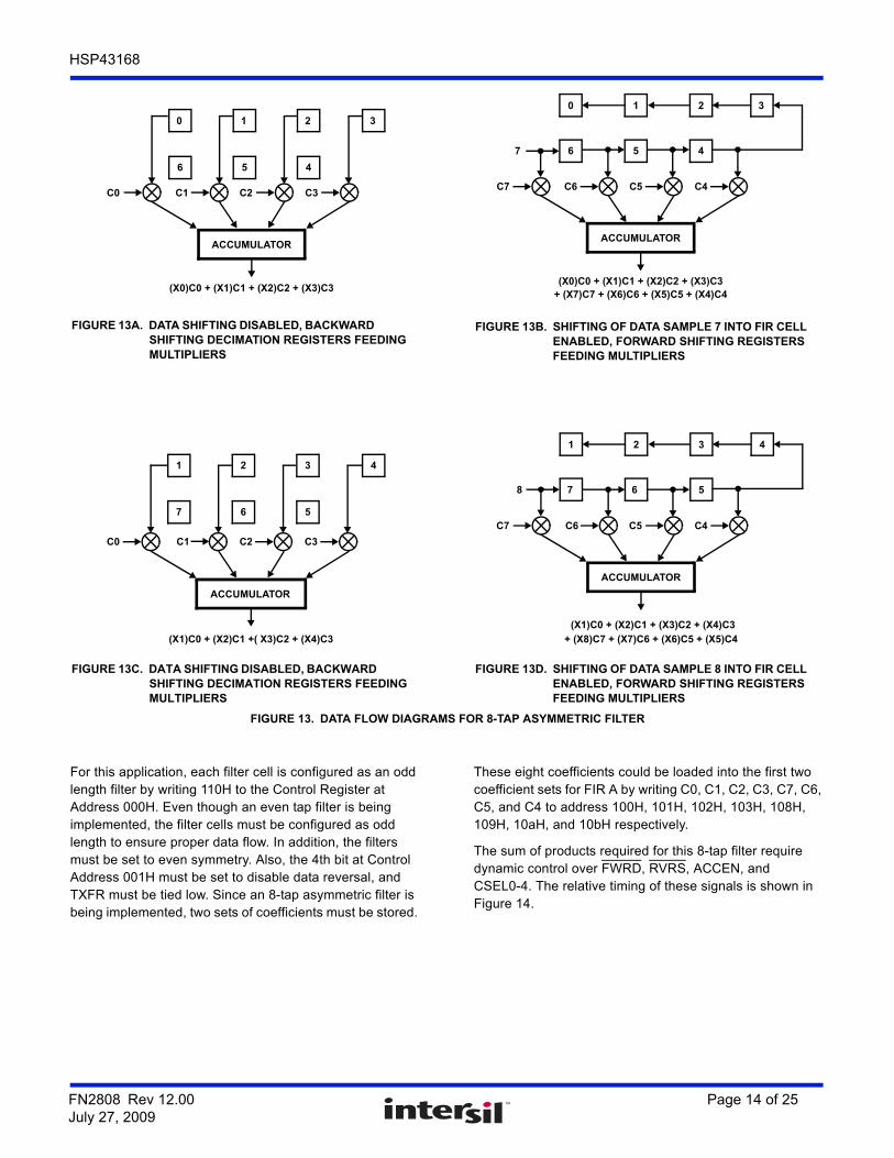
For this application, each filter cell is configured as an odd length filter by writing 110H to the Control Register at Address 000H. Even though an even tap filter is being implemented, the filter cells must be configured as odd length to ensure proper data flow. In addition, the filters must be set to even symmetry. Also, the 4th bit at Control Address 001H must be set to disable data reversal, and TXFR must be tied low. Since an 8-tap asymmetric filter is being implemented, two sets of coefficients must be stored.
These eight coefficients could be loaded into the first two coefficient sets for FIR A by writing C0, C1, C2, C3, C7, C6, C5, and C4 to address 100H, 101H, 102H, 103H, 108H, 109H, 10aH, and 10bH respectively.
The sum of products required for this 8-tap filter require dynamic control over FWRD, RVRS, ACCEN, and CSEL0-4. The relative timing of these signals is shown in Figure 14.
FIGURE 13A. DATA SHIFTING DISABLED, BACKWARD SHIFTING DECIMATION REGISTERS FEEDING MULTIPLIERS
FIGURE 13B. SHIFTING OF DATA SAMPLE 7 INTO FIR CELL ENABLED, FORWARD SHIFTING REGISTERS FEEDING MULTIPLIERS
FIGURE 13C. DATA SHIFTING DISABLED, BACKWARD SHIFTING DECIMATION REGISTERS FEEDING MULTIPLIERS
FIGURE 13D. SHIFTING OF DATA SAMPLE 8 INTO FIR CELL ENABLED, FORWARD SHIFTING REGISTERS FEEDING MULTIPLIERS
FIGURE 13. DATA FLOW DIAGRAMS FOR 8-TAP ASYMMETRIC FILTER
6 5 4
0 1 2 3
C0 C1 C2 C3
(X0)C0 + (X1)C1 + (X2)C2 + (X3)C3
ACCUMULATOR
6 5 4
0 1 2 3
C7 C6 C5 C4
ACCUMULATOR
7
(X0)C0 + (X1)C1 + (X2)C2 + (X3)C3+ (X7)C7 + (X6)C6 + (X5)C5 + (X4)C4
7 6 5
1 2 3 4
C0 C1 C2 C3
(X1)C0 + (X2)C1 +( X3)C2 + (X4)C3
ACCUMULATOR
ACCUMULATOR
7 6 5
1 2 3 4
C7 C6 C5 C4
8
(X1)C0 + (X2)C1 + (X3)C2 + (X4)C3
+ (X8)C7 + (X7)C6 + (X6)C5 + (X5)C4
FN2808 Rev 12.00 Page 14 of 25July 27, 2009

HSP43168
Example 4: Even-Tap Decimating Filter Example
The HSP43168 supports filtering applications requiring decimation to 16. In these applications the output data rate is reduced by a factor of N. As a result, N clock cycles can be used for the computation of the filter output. For example, each FIR cell can calculate 8 symmetric or 4 asymmetric taps in one clock. If the application requires decimation by two, the filter output can be calculated over two clocks thus, boosting the number of taps per FIR cell to 16 symmetric or 8 asymmetric. For this example, each FIR cell is configured as an independent 24-tap decimate x3 filter. Again, the data flow diagrams show only one of the FIR cells shown in Figure 15.
The alignment of data relative to the 24 filter coefficients for a particular output is depicted graphically in Figure 16. As in previous examples, the HSP43168 implements the filtering operation by summing data samples prior to multiplication by the common coefficient. In this example an output is required every third CLK which allows 3 CLKs for computation. On each CLK, one of three sets of coefficients are used to calculate 8 of the filter taps. The Block Diagrams in Figure 17 show the data flow and accumulator output for the data/coefficient alignment in Figure 16.
Proper data and coefficient alignment is achieved by asserting TXFR once every three CLKs to switch the LIFOs which are being read and written. This has the effect of feeding blocks of three samples into the backward shifting decimation path which are reversed in sample order. In addition, ACCEN is deasserted once every three clocks to allow accumulation over three CLKs. The three sets of coefficients required in the calculation of a 24-tap symmetric filter are cycled through using CSEL0-4. The timing relationship between the CSEL0-4, ACCEN, and TXFR are shown in Figure 18.
To operate in this mode the Dual is configured by writing 1d2 to Address 000H via the microprocessor interface, CIN0-9, A0-8, and WR. Data reversal must be enabled see (Table 2). The 12 unique coefficients for this example are stored as three sets of coefficients for either FIR cell. For FIR A, the coefficients are loaded into the Coefficient Bank by writing C2, C5, C8, C11, C1, C4, C7, C10, C0, C3, C6, and C9 to Address [100H, 101H, 102H, 103H], CSEL = 0; [108H, 109H, 10aH, 10bH], CSEL = 1; [110H, 111H, 112H, and 113H], CSEL = 2, respectively.
0 1 2 3 13 14 15 16
X0 X1
1 0 1 0 0 1 1 0
X6 X7 X8
CLK
INA0-9
CSEL0-4
ACCEN
SHFTEN
RVRS
FWRD
0
NOTE: CLK is 2X data rate.
FIGURE 14. CONTROL TIMING FOR 8-TAP ASYMMETRICFILTER
TXFR (TIED LOW)
(NOTE)
FIGURE 15. EVEN-TAP DECIMATING FILTER, 24-TAP DEC = 3 FIGURE 16. DATA/COEFFICIENT ALIGNMENT FOR 24-TAP DECIMATE BY 3 FIR FILTER
HSP43168
INA0-9
INB0-9
OUT9-27
FIR A
FIR B
MUX
EVEN-TAP DECIMATING
EVEN-TAP DECIMATINGA A
B B
23 22 21 20 19 18 17 16 15 14 13 12 11 10 9 8 7 6 5 4 3 2 1 0
C11C10C9C8C7C6C5C4C3C2C1C0
h(n)
C11C10 C9 C8 C7 C6 C5 C4 C3 C2 C1 C0
24-TAPS
x(n)
FN2808 Rev 12.00 Page 15 of 25July 27, 2009

HSP43168
Example 5: Odd-Tap Decimating Symmetric Filter
This example highlights the use of the HSP43168 as two independent, 23-tap, symmetric, decimate by 3 filters. In this example, the operational differences in the control signals and data reversal structure may be compared to the previously discussed even-tap decimating filter. Figure 19 shows two FIR cells. The data flow in this example uses only one of the FIR cells.
FIGURE 17A. COMPUTATIONAL FLOW AS DATA SAMPLE 21 IS CLOCKED INTO THE FEED-FORWARD STAGE
FIGURE 17B. COMPUTATIONAL FLOW AS DATA SAMPLE 22 IS CLOCKED INTO THE FEED-FORWARD STAGE
FIGURE 17C. COMPUTATIONAL FLOW AS DATA SAMPLE 23 IS CLOCKED INTO THE FEED-FORWARD STAGE
FIGURE 17D. COMPUTATIONAL FLOW AS DATA SAMPLE 24 IS CLOCKED INTO THE FEED-FORWARD STAGE
FIGURE 17. DATA FLOW DIAGRAMS FOR 24-TAP DECIMATED BY 3 FIR FILTER
+ + + +
ACCUMULATOR
C2 C5 C8 C11
678 91011
21
(X2 + X21)C2 + (X5 + X18)C5 + (X8 + X15)C8 + (X11 + X12)C11
CSEL = 0
121314
345
151617
012
181920+ + + +
ACCUMULATOR
C1 C4 C7 C10
501 834 1167
192021 161718 131415
910
22
12
(X1 + X22)C1 + (X4 + X19)C4 + (X7 + X16)C7 + (X10 + X13)C10+(X2 + X21)C2 + (X5 + X18)C5 + (X8 + X15)C8 + (X11 + X12)C11
CSEL = 1
+ + + +
ACCUMULATOR
C0 C3 C6 C9
450 783
202122 171819 14151623
10116
12 13
9
(X0 + X23)C0 + (X3 + X20)C3 + (X6 + X17)C6 + (X9 + X14)C9+ (X1 + X22)C1 + (X4 + X19)C4 + (X7 + X16)C7 + (X10 + X13)C10+ (X2 + X21)C2 + (X5 + X18)C5 + (X8 + X15)C8 + (X11 + X12)C11
CSEL = 2
ACCEN ASSERTEDAND ACTIVE
TXFR ASSERTEDAND ACTIVE
+ + + +
ACCUMULATOR
C2 C5 C8 C11
345 678
212223 181920 15161724
91011
13 12
(X5 + X24)C0 + (X8 + X21)C5 + (X11 + X18)C8 + (X14 + X15)C11
14
CSEL = 0
0 1 2 3 5 21 22 23
0
0 1 2 0
CLK
INA0-9
CSEL0-4
ACCEN
TXFR
1 2 3 4 5
4
22 2321
1 2 0 1 2
†Tied low.
FIGURE 18. CONTROL SIGNAL TIMING FOR 24-TAPDECIMATE X3 FILTER
FWRD†
RVRS†
SHIFTEN†
HSP43168
INA0-9
INB0-9
OUT9-27
FIR A
FIR B
MUX
FIGURE 19. USING HSP43168 AS TWO INDEPENDENT FILTERS
ODD-TAP DECIMATING
ODD-TAP DECIMATINGA A
B B
FN2808 Rev 12.00 Page 16 of 25July 27, 2009

HSP43168
As in the 24-tap example, an output is required every third CLK which allows 3 CLKs for computation. On each CLK, one of three sets of coefficients are used to calculate the filter taps. Since this is an odd length filter, the center coefficient must be scaled by 1/2 to compensate for the summation of the same data sample from the forward and backward shifting decimation paths. The Block Diagrams in Figure 20 show the data flow, and the accumulator output for the data coefficient alignment is shown in Figure 21.
Proper data and coefficient alignment is achieved by asserting TXFR once every three CLKs to switch the LIFOs which are being read and written. In the odd-tap mode, TXFR is internally delayed by one clock cycle with respect to ACCEN so that the convolutional sum will be computed correctly. For odd length filters, data prior to the last register in the forward decimation path is routed to the feedback circuitry. As a result, TXFR should be asserted one cycle prior to the input data samples which align with the center tap. The timing relationship between the CSEL0-5, ACCEN, and TXFR are shown in Figure 22.
FIGURE 20A. COMPUTATIONAL FLOW AS DATA SAMPLE 21 IS CLOCKED INTO THE FEED-FORWARD STAGE TXFR TAKES AFFECT ON THIS CLOCK CYCLE
FIGURE 20B. COMPUTATIONAL FLOW AS DATA SAMPLE 22 IS CLOCKED INTO THE FEED-FORWARD STAGE
FIGURE 20C. COMPUTATIONAL FLOW AS DATA SAMPLE 23 IS CLOCKED INTO THE FEED-FORWARD STAGE
FIGURE 20D. COMPUTATIONAL FLOW AS DATA SAMPLE 24 IS CLOCKED INTO THE FEED-FORWARD STAGE TXFR TAKES AFFECT ON THIS CLOCK CYCLE
FIGURE 20. DATA FLOW DIAGRAMS FOR 23-TAP DECIMATE BY 3 SYMMETRIC FILTER
+ + + +
ACCUMULATOR
C2 C5 C8 C11/2
123 456
181920 151617 12131421
(X3 + X21)C2 + (X6 + X18)C5 + (X9 + X15)C8 + (X12 + X12)C11/2
789 11 1012
CSEL = 0
+ + + +
ACCUMULATOR
C1 C4 C7 C10
612 945 1278
192021 161718 131415
1011
22
13
(X2 + X22)C1 + (X5 + X19)C4 + (X8 + X16)C7 + (X11 + X13)C10
+ (X3 + X21)C2 + (X6 + X18)C5 + (X9 + X15)C8 + (X12 + X12)C11/2
CSEL = 1
+ + + +
ACCUMULATOR
C0 C3 C6 C9
561 894
202122 171819 14151623
1112713 14
10
(X1 + X23)C0 + (X4 + X20)C3 + (X7 + X17)C6 + (X14 + X10)C9+ (X2 + X22)C1 + (X5 + X19)C4 + (X8 + X16)C7 + (X11 + X13)C10
+ (X3 + X21)C2 + (X6 + X18)C5 + (X9 + X15)C8 + (X12 + X12)C11/2
ACCEN ASSERTEDAND ACTIVE
TXFR ASSERTED
CSEL = 2
+ + + +
ACCUMULATOR
C2 C5 C8 C11/2
456 789
212223 181920 15161724
101112 14 13
(X6 + X24)C2 + (X9 + X21)C5 + (X12 + X18)C8 + (X15 + X15)C11/2
15
CSEL = 0
FN2808 Rev 12.00 Page 17 of 25July 27, 2009

HSP43168
To operate in this mode, the Dual is configured by writing 112H to Address 000H via the microprocessor interface, CIN0-9, A0-8, and WR. Data reversal must be enabled (see Table 2). The 12 unique coefficients for this example are stored as three sets of coefficients for either FIR cell. For FIR A, the coefficients are loaded into the Coefficient Bank by writing [C2, C5, C8, (C11)/ 2], CSEL = 0; [C1, C4, C7, C10], CSEL = 1; [C0, C3, C6, and C9], CSEL = 2; to address 100H, 101H, 102H, 103H, 108H, 109H, 10aH, 10bH, 110H, 111H, 112H, and 113H, respectively.
Example 6. Dual Decimation Example
The purpose of this example is to give an overview of one of the more complex applications of the HSP43168. The input is two data streams (A) and (B) samples. Figure 23 shows the upper level block diagram of the system being implemented. The decimation rate was set to N. N-1 is loaded into the decimation factor in Control Word 000H.
To demonstrate the muxed decimation, lets suppose that the application requires filter A to be configured as an even-decimate-by-3 filter and filter B to be configured as a odd-decimate-by-3 filter. The output data is made of the two decimated data streams multiplexed together and has a data rate equal to 2x the input sampling rate divided by the decimation factor. Figure 24 shows the data/coefficient alignment for FIR A and FIR B.
To operate in this mode, Control Word 000H must be written with a 0x152. Data reversal must be enabled by setting bit 4 of Control Word 001H = 0. The filter set selected by CSEL0-4 = 0 should be loaded by writing C2, C5, C8, C11, D2, D5, D8, and (D11)/ 2 into 100H, 101H, 102H, 103H, 104H, 105H, 106H, and 107H. The filter set selected by CSEL0-4 = 1 should be loaded by writing C1, C4, C7, C10, D1, D4, D7, and D10 into 108H, 109H, 10aH, 10bH, 10cH, 10dH, 10eH, and 10fH. The filter set selected by CSEL0-4 = 2 should be loaded by writing C0, C3, C6, C9, D0, D3, D6, and D9 into 110H, 111H, 112H, 113H, 114H, 115H, 116H, and 117H.
C10C9 C8 C7 C6 C5 C4C3 C2 C1 C0
C10C9C8C7C6C5C4C3C2C1C0
C11
FIGURE 21. DATA/COEFFICIENT ALIGNMENT FOR 23-TAPDECIMATE BY 3 SYMMETRIC FILTER
h(n)
23 22 21 20 19 18 17 16 15 14 13 12 11 10 9 8 7 6 5 4 3 2 1 0
x(n)
23-TAPS
0 1 2 3 5 20 21 22
0
0 1 2 0
CLK
INA0-9
CSEL0-4
ACCEN
TXFR
1 2 3 4 5
4
22 2321
1 2 0 1 2
†Tied low.
FIGURE 22. CONTROL SIGNAL TIMING FOR 23-TAP SYMMETRIC FILTER
FWRD†
RVRS†
SHIFTEN†
A3, A2, A1, A0
B3, B2, B1, B0
HSP43168
INB0-9
INA0-9
FS
DECIMATE BY N
2FS/(N+1)
OUT9-27
AOUT1BOUT0AOUT0
BOUT1
FIGURE 23. MULTIPLEXED DECIMATION BLOCK DIAGRAM
FN2808 Rev 12.00 Page 18 of 25July 27, 2009

HSP43168
Figure 25 shows the Timing Diagram required to obtained the multiplexed/decimated output. The output of the two filters are provided at by selecting the odd-decimation filter first, then the even-decimation second using MUX0-1. Figure 26 shows the Data Flow Diagram for the multiplexed decimation example.
h2(n)
FIRB
FIRA
FIGURE 24. DATA/COEFFICIENT ALIGNMENT FOR MULTIPLEXED DECIMATION EXAMPLE
D10 D9 D8 D7 D6 D5 D4 D3 D2 D1 D0
D10D9D8D7D6D5D4D3D2D1D0
D11
23 22 21 20 19 18 17 16 15 14 13 12 11 10 9 8 7 6 5 4 3 2 1 0
23 22 21 20 19 18 17 16 15 14 13 12 11 10 9 8 7 6 5 4 3 2 1 0
C11C10C9C8C7C6C5C4C3C2C1C0
h1(n)
C11C10C9 C8 C7 C6 C5 C4 C3 C2 C1 C0
23-TAPS
B(n)
24-TAPS
A(n)
0 1 2 3 5 20 21 22
0
0 1 2 0
CLK
INA0-9
CSEL0-4
TXFR
1 2 3 4 5
4
21 2220
1 2 2 0 1
11 10 11 11 1110MUX0-1
ACCEN
FIGURE 25. TIMING DIAGRAM FOR MULTIPLEXED DECIMATION EXAMPLE
FIGURE 26A. COMPUTATIONAL FLOW AS DATA SAMPLE 21 IS CLOCKED INTO THE FEED-FORWARD STAGE
FIGURE 26B. COMPUTATIONAL FLOW AS DATA SAMPLE 22 IS CLOCKED INTO THE FEED-FORWARD STAGE
+ + + +
ACCUMULATOR
D2 D5 D8 D11/2
123 456
181920 151617 12131421
789 11 1012
CSEL = 0
(X3 + X21)D2 + (X6 + X18)D5 + (X9 + X15)D8 + (X12 + X12)D11/2
B DATA
FIR B
+ + + +
ACCUMULATOR
C2 C5 C8 C11
678 91011
21
CSEL = 0
121314
345
151617
012
181920
(X2 + X21)C2 + (X5 + X18)C5 + (X8 + X15)C8 + (X11 + X12)C11
FIR A
STREAM
A DATASTREAM
+ + + +
ACCUMULATOR
D1 D4 D7 D10
612 945 1278
192021 161718 131415
1011
22
13
CSEL = 1
(X2 + X22)D1 + (X5 + X19)D4 + (X8 + X16)D7 + (X11 + X13)D10
+ (X3 + X21)D2 + (X6 + X18)D5 + (X9 + X15)D8 + (X12 + X12)D11/2
FIR B
+ + + +
ACCUMULATOR
C1 C4 C7 C10
501 834 1167
192021 161718 131415
910
22
12
CSEL = 1
(X1 + X22)C1 + (X4 + X19)C4 + (X7 + X16)C7 + (X10 + X13)C10+(X2 + X21)C2 + (X5 + X18)C5 + (X8 + X15)C8 + (X11 + X12)C11
FIR A
FN2808 Rev 12.00 Page 19 of 25July 27, 2009

HSP43168
FIGURE 26C. COMPUTATIONAL FLOW AS DATA SAMPLE 23 IS CLOCKED INTO THE FEED-FORWARD STAGE
FIGURE 26D. COMPUTATIONAL FLOW AS DATA SAMPLE 24 IS CLOCKED INTO THE FEED-FORWARD STAGE
FIGURE 26. DATA FLOW DIAGRAM FOR MULTIPLEXED DECIMATION EXAMPLE
+ + + +
ACCUMULATOR
D0 D3 D6 D9
561 894
202122 171819 14151623
1112713 14
10
OUTPUT OF B IS SENTTO OUT9-27
CSEL = 2
FIR B
(X1 + X23)D0 + (X4 + X20)D3 + (X7 + X17)D6 + (X14 + X10)D9+ (X2 + X22)D1 + (X5 + X19)D4 + (X8 + X16)D7 + (X11 + X13)D10
+ (X3 + X21)D2 + (X6 + X18)D5 + (X9 + X15)D8 + (X12 + X12)D11/2
+ + + +
ACCUMULATOR
C0 C3 C6 C9
450 783
202122 171819 14151623
10116
12 13
9
CSEL = 2
(X0 + X23)C0 + (X3 + X20)C3 + (X6 + X17)C6 + (X9 + X14)C9+ (X1 + X22)C1 + (X4 + X19)C4 + (X7 + X16)C7 + (X10 + X13)C10+ (X2 + X21)C2 + (X5 + X18)C5 + (X8 + X15)C8 + (X11 + X12)C11
FIR A
+ + + +
ACCUMULATOR
D2 D5 D8 D11/2
456 789
212223 181920 15161724
101112 14 13
(X6 + X24)D2 + (X9 + X21)D5 + (X12 + X18)D8 + (X15 + X15)D11/2
15
CSEL = 0
FIR B
+ + + +
ACCUMULATOR
C2 C5 C8 C11
345 678
212223 181920 15161724
91011
13 1214
CSEL = 0
(X5+X24)C0+(X8+X21)C5+(X11+X18)C8+(X14+X15)C11
OUTPUT OF A IS SENTTO OUT9-27
FIR A
FN2808 Rev 12.00 Page 20 of 25July 27, 2009

HSP43168
Absolute Maximum Ratings Thermal Information
Supply Voltage . . . . . . . . . . . . . . . . . . . . . . . . . . . . . . . . . . . . . +6.0VInput, Output or I/O Voltage . . . . . . . . . . . . GND -0.5V to VCC +0.5VESD Classification . . . . . . . . . . . . . . . . . . . . . . . . . . . . . . . . . Class 1
Operating ConditionsVoltage Range . . . . . . . . . . . . . . . . . . . . . . . . . . . . . . . . . . . 5V 5%Temperature Range, Commercial . . . . . . . . . . . . . . . . 0°C to +70°CTemperature Range, Industrial. . . . . . . . . . . . . . . . . .-40°C to +85°C
Die CharacteristicsBack Side Potential . . . . . . . . . . . . . . . . . . . . . . . . . . . . . . . . . . .+5VNumber of Transistors or Gates. . . . . . . . . . . . . . . . . . . . . . . . 32529
Thermal Resistance (Typical, Note 2) . . . . . . . . . . . . . JA (°C/W)MQFP Package . . . . . . . . . . . . . . . . . . . . . . . . . . . . 33PLCC Package. . . . . . . . . . . . . . . . . . . . . . . . . . . . . 24
Maximum Junction TemperatureMQFP and PLCC Packages . . . . . . . . . . . . . . . . . . . . . . . +150°C
Maximum Storage Temperature Range . . . . . . . . . . -65°C to +150°CPb-Free Reflow Profile. . . . . . . . . . . . . . . . . . . . . . . . .see link below
http://www.intersil.com/pbfree/Pb-FreeReflow.asp
CAUTION: Do not operate at or near the maximum ratings listed for extended periods of time. Exposure to such conditions may adversely impact product reliability andresult in failures not covered by warranty
NOTE:
2. JA is measured in free air with the component mounted on a high effective thermal conductivity test board with “direct attach” features. See Tech Brief TB379.
DC Electrical Specifications
PARAMETER SYMBOL TEST CONDITIONS MIN MAX UNITS
Power Supply Current ICCOP VCC = Max (Notes 4, 5, 6)CLK Frequency 33MHz
- 363 mA
Standby Power Supply Current ICCSB VCC = Max, Outputs Not Loaded - 500 µA
Input Leakage Current II VCC = Max, Input = 0V or VCC -10 10 µA
Output Leakage Current IO VCC = Max, Input = 0V or VCC -10 10 µA
Logical One Input Voltage VIH VCC = Max 2.0 - V
Logical Zero Input Voltage VIL VCC = Min - 0.8 V
Logical One Output Voltage VOH IOH = -400µA, VCC = Min 2.6 - V
Logical Zero Output Voltage VOL IOL = 2mA, VCC = Min - 0.4 V
Clock Input High VIHC VCC = Max 3.0 - V
Clock Input Low VILC VCC = Min - 0.8 V
Input Capacitance CIN CLK Frequency 1MHzAll measurements referencedto GND. TA = +25°C, (Note 3)
- 12 pF
Output Capacitance COUT - 12 pF
NOTES:
3. Controlled via design or process parameters and not directly tested. Characterized upon initial design and after major process and/or changes.
4. Power Supply current is proportional to operating frequency. Typical rating for ICCOP is 11mA/MHz.
5. Output load per test load circuit and CL = 40pF.
6. Maximum junction temperature must be considered when operating part at high clock frequencies.
FN2808 Rev 12.00 Page 21 of 25July 27, 2009

HSP43168
AC Test Load Circuit
AC Electrical Specifications VCC = +4.75V to +5.25V, TA = 0°C to +70°C Commercial, TA = -40°C to +85°C Industrial (Note 7)
PARAMETER SYMBOL NOTES
-33 (33MHz) -40 (40.8MHz) -45 (45MHz)
UNITSMIN
(Note 11)MAX
(Note 11)MIN
(Note 11)MAX
(Note 11)MIN
(Note 11)MAX
(Note 11)
CLK Period tCP 30 - 24.5 - 22 - ns
CLK High tCH 12 - 10 - 8 - ns
CLK Low tCL 12 - 10 - 8 - ns
WR Period tWP 30 - 24.5 - 22 - ns
WR High tWH 12 - 10 - 10 - ns
WR Low tWL 12 - 10 - 10 - ns
Setup Time A0-8 to WR Going Low tAWS 10 - 8 - 8 - ns
Hold Time A0-8 from WR Going High tAWH 0 - 0 - 0 - ns
Setup Time CIN0-9 to WR Going High tCWS 12 - 11 - 10 - ns
Hold Time CIN0-9 from WR Going High tCWH 1 - 1 - 1 - ns
Setup Time WR Low to CLK Low tWLCL (Note 8) 5 - 4 - 3 - ns
Setup Time CIN0-9 to CLK Low tCVCL (Note 8) 7 - 7 - 7 - ns
Setup Time CSEL0-5, SHFTEN, FWRD, RVRS, TXFR, INA0-9, INB0-9, ACCEN, MUX0-1 to CLK Going High
tECS 15 - 13 - 12 - ns
Hold Time CSEL0-5, SHFTEN, FWRD, RVRS, TXFR, INA0-9, INB0-9, ACCEN, MUX0-1 to CLK Going High
tECH 0 - 0 - 0 - ns
CLK to Output Delay OUT0-27 tDO - 14 - 13 - 12 ns
Output Enable Time tOE - 12 - 12 - 12 ns
Output Disable Time tOD (Note 9) - 12 - 12 - 12 ns
Output Rise, Fall Time tRF (Note 9) - 6 - 6 - 6 ns
NOTES:
7. AC tests performed with CL = 40pF, IOL = 2mA, and IOH = -400µA. Input reference level CLK = 2.0V. Input reference level for all other inputs is 1.5V. Test VIH = 3.0V, VIHC = 4.0V, VIL = 0V, VILC = 0V.
8. Setup time requirement for loading of data on CIN0-9 to guarantee recognition on the following clock.
9. Controlled via design or process parameters and not directly tested. Characterized upon initial design and after major process and/or changes.
10. Parameters with MIN and/or MAX limits are 100% tested at +25°C, unless otherwise specified. Temperature limits established by characterization and are not production tested.
11. Parameters with MIN and/or MAX limits are 100% tested at +25°C, unless otherwise specified. Temperature limits established by characterization and are not production tested.
EQUIVALENT CIRCUIT
CL (NOTE)
IOH 1.5V IOL
DUT
SWITCH S1 OPEN FOR ICCSB AND ICCOP
S1
Note: Test head capacitance.
FN2808 Rev 12.00 Page 22 of 25July 27, 2009

HSP43168
Waveforms
FIGURE 27. OUTPUT ENABLE, DISABLE TIMING
FIGURE 28. OUTPUT RISE AND FALL TIMES
tECS tECH
tDO
CLK
OUT0 - 27
tWHtWL
tWP
WR
tWLCL
tAWS tAWH
A0 - 8
tCWHtCWS
CIN0 - 9
tCVCL
tCP
tCLtCH
CSEL0 - 4, MUX0 - 1
INA0 - 9, INB0 - 9,ACCEN
SHFTEN, FWRD
RVRS, TXFR
1.5V
1.7V1.3V
1.5V
HIGHIMPEDANCE
HIGHIMPEDANCE
OUT0 - 27
OEL, OEH
tOE tOD
tRF
2.0V
0.8V
2.0V
0.8V
tRF
FN2808 Rev 12.00 Page 23 of 25July 27, 2009

HSP43168
Metric Plastic Quad Flatpack Packages (MQFP)
D
D1
E E1
-A-
PIN 1
A2 A1
A
12o-16o
12o-16o
0o-7o
0.400.016 MIN
L
0o MIN
PLANE
b
0.005/0.0090.13/0.23
WITH PLATING
BASE METAL
SEATING
0.005/0.0070.13/0.17
b1
-B-
e
0.0080.20 A-B SD SCM
0.0760.003
-C-
-D-
-H-
Q100.14x20 (JEDEC MS-022GC-1 ISSUE B)100 LEAD METRIC PLASTIC QUAD FLATPACK PACKAGE
SYMBOL
INCHES MILLIMETERS
NOTESMIN MAX MIN MAX
A - 0.134 - 3.40 -
A1 0.010 - 0.25 - -
A2 0.101 0.113 2.57 2.87 -
b 0.009 0.015 0.22 0.38 6
b1 0.009 0.013 0.22 0.33 -
D 0.908 0.918 23.08 23.32 3
D1 0.782 0.792 19.88 20.12 4, 5
E 0.673 0.681 17.10 17.30 3
E1 0.547 0.555 13.90 14.10 4, 5
L 0.029 0.040 0.73 1.03 -
N 100 100 7
e 0.026 BSC 0.65 BSC -
ND 30 30 -
NE 20 20 -
Rev. 1 4/99NOTES:
1. Controlling dimension: MILLIMETER. Converted inch dimensions are not necessarily exact.
2. All dimensions and tolerances per ANSI Y14.5M-1982.
3. Dimensions D and E to be determined at seating plane .
4. Dimensions D1 and E1 to be determined at datum plane .
5. Dimensions D1 and E1 do not include mold protrusion. Allowable protrusion is 0.25mm (0.010 inch) per side.
6. Dimension b does not include dambar protrusion. Allowable dambar protrusion shall be 0.08mm (0.003 inch) total.
7. “N” is the number of terminal positions.
-C-
-H-
FN2808 Rev 12.00 Page 24 of 25July 27, 2009

FN2808 Rev 12.00 Page 25 of 25July 27, 2009
HSP43168
Intersil products are manufactured, assembled and tested utilizing ISO9001 quality systems as notedin the quality certifications found at www.intersil.com/en/support/qualandreliability.html
Intersil products are sold by description only. Intersil may modify the circuit design and/or specifications of products at any time without notice, provided that such modification does not, in Intersil's sole judgment, affect the form, fit or function of the product. Accordingly, the reader is cautioned to verify that datasheets are current before placing orders. Information furnished by Intersil is believed to be accurate and reliable. However, no responsibility is assumed by Intersil or its subsidiaries for its use; nor for any infringements of patents or other rights of third parties which may result from its use. No license is granted by implication or otherwise under any patent or patent rights of Intersil or its subsidiaries.
For information regarding Intersil Corporation and its products, see www.intersil.com
For additional products, see www.intersil.com/en/products.html
© Copyright Intersil Americas LLC 2000-2009. All Rights Reserved.All trademarks and registered trademarks are the property of their respective owners.
Plastic Leaded Chip Carrier Packages (PLCC)
NOTES:
1. Controlling dimension: INCH. Converted millimeter dimensions are not necessarily exact.
2. Dimensions and tolerancing per ANSI Y14.5M-1982.
3. Dimensions D1 and E1 do not include mold protrusions. Allowable mold protrusion is 0.010 inch (0.25mm) per side. Dimensions D1and E1 include mold mismatch and are measured at the extremematerial condition at the body parting line.
4. To be measured at seating plane contact point.
5. Centerline to be determined where center leads exit plastic body.
6. “N” is the number of terminal positions.
-C-
A1
A
SEATINGPLANE
0.020 (0.51)
MIN
VIEW “A”
D2/E2
0.025 (0.64)0.045 (1.14)
R
0.042 (1.07)0.056 (1.42)
0.050 (1.27) TP
EE1
0.042 (1.07)0.048 (1.22)
PIN (1) IDENTIFIER
CL
D1D
0.020 (0.51) MAX
3 PLCS 0.026 (0.66)0.032 (0.81)
0.045 (1.14)
MIN
0.013 (0.33)
0.021 (0.53)
0.025 (0.64)
MIN
VIEW “A” TYP.
0.004 (0.10) C
-C-
D2/E2
CL
N84.1.15 (JEDEC MS-018AF ISSUE A)84 LEAD PLASTIC LEADED CHIP CARRIER PACKAGE
SYMBOL
INCHES MILLIMETERS
NOTESMIN MAX MIN MAX
A 0.165 0.180 4.20 4.57 -
A1 0.090 0.120 2.29 3.04 -
D 1.185 1.195 30.10 30.35 -
D1 1.150 1.158 29.21 29.41 3
D2 0.541 0.569 13.75 14.45 4, 5
E 1.185 1.195 30.10 30.35 -
E1 1.150 1.158 29.21 29.41 3
E2 0.541 0.569 13.75 14.45 4, 5
N 84 84 6
Rev. 2 11/97