Embed Size (px)
Citation preview

TU: PN junction Subject: Physics Class: 5 C - 20 students aged 18/19 Language level : B1 / B2 Teacher: Laurena Petrizzi
STEP 1. a. INTRODUCTION AND MOTIVATIONElectronics is very, very useful in a lot of applications.
Think, for example, about the reception of a signal and its further processing like the decoding of the speed of a motorbike: a high-speed microprocessor inside a little box uses a digital software to encode the electrical pulse from the vehicle speed sensor.
A physical quantity like a sound, a picture, pressure, temperature is usually converted, by a transducer, into an electrical signal that can be amplified, transmitted and received. That is what happens for example in a sound transmission.
Nowadays most signals that measure real physical conditions are sampled into digital numeric values that can be manipulated by a computer.
Laurena Petrizzi LS A. Oriani Ravenna 1
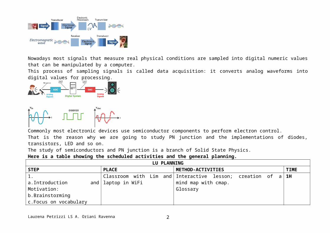
This process of sampling signals is called data acquisition: it converts analog waveforms into digital values for processing.
Commonly most electronic devices use semiconductor components to perform electron control. That is the reason why we are going to study PN junction and the implementations of diodes, transistors, LED and so on.The study of semiconductors and PN junction is a branch of Solid State Physics.Here is a table showing the scheduled activities and the general planning.
LU PLANNINGSTEP PLACE METHOD-ACTIVITIES TIME1.a.Introduction and Motivation:b.Brainstormingc.Focus on vocabulary
Classroom with Lim and laptop in WiFi
Interactive lesson; creation of a mind map with cmap.Glossary
1H
2.Lecture Ifrom 1 to 24 slide
Classroom with Lim and laptop in WiFi
Interactive lesson: presentation with Prezi;download of the ppt version for students;discussion and questions.
1,5H+0,5H
3.a.Video PN junction slide 25b.Crossword activityc.FCE activity
Classroom with Lim and laptop in WiFi
Revision with a videoConsolidation activities in group work
1H
4.Lecture IIfrom 26 to 37 slide
Classroom with Lim and laptop in WiFi
Interactive lesson: presentation with Prezi;discussion and questions.
2,0H+0,5H
5.Written test I Classroom with Lim and laptop in WiFi
Individual test: problem solving, fill in, true/false, multiple choice activitiesAssessment: rubric enclosed
1H
6.a.Video Transistors slide 38
IT Laboratory A video aimed at a deeper learning of the topicGroup work aimed at a presentation for the oral test
1,5H
Laurena Petrizzi LS A. Oriani Ravenna 2

b.Webquest Search for information in the web7.Oral test: presentation about transistors
Classroom with Lim and laptop in WiFi
Group workCreation of an interactive product Assessment: rubric enclosed
2H
Further written test Classroom Problem solving for the simulation of Terza Prova 1HFurther oral test Classroom with Lim and laptop in
WiFiKnowledge, skills, competencesAssessment: rubric enclosed
3H
STEP 1. b. BRAINSTORMINGThe map introduces the basic glossary related to PN junction and to the topics to be developed. It is also a hint for further key words students can suggest and a way to enlarge their scientific vocabulary.
Laurena Petrizzi LS A. Oriani Ravenna 3

STEP 1. c. FOCUS VOCABULARYThis step is aimed at consolidating the vocabulary necessary to fully understand the teacher’s lectures.
GLOSSARYBand gap=the difference in energy between electron orbitals in which the electrons are not free to move (called valence bands) and orbitals in which they are relatively free and can carry a current (called conduction bands).
Blur=become visually indistinct.
Breakdown=the abrupt failure of an insulator or insulating medium to restrict the flow of current.
Buildup=to form by combining materials or parts; construct.
Cease=put an end to, to come to an end. Clip=cut, cut off.
Conduction band=the set of electron orbitals, generally the outermost shells of the atoms in a conductor or semiconductor, in which electrons are free to move and thereby carry an electric current.
Departure=the act or an instance of departing.
Depletion layer=a region at the interface between dissimilar zones of conductivity in a semiconductor, in which there are few charge carriers.
Device=a machine or tool used for a specific task.
Diode=an electronic device that restricts current flow chiefly to one direction.
Dope=treat a semiconductor with an additive, dopant, used to improve its properties.
Dramatic =striking; effective
Dramatically=in a very impressive manner
Drop=In electronics to fall from a higher to a lower electric potential.
Laurena Petrizzi LS A. Oriani Ravenna 4

Extrinsic semiconductor =an extrinsic semiconductor is a semiconductor that has been doped, that is, into which a doping agent has been introduced, giving it different electrical properties than the intrinsic (pure) semiconductor.
Fermi level=the top of the available electron energy levels at low temperatures.
Forwardbias=a voltage applied to a circuit or device, esp. a semiconductor device, in the direction that produces the larger current.
Hole=a vacant position in an atom left by the absence of a valence electron.
Intrinsic=a semiconductor which is not doped.
Intrinsic semiconductor=an almost pure semiconductor to which no impurities have been added and in which the electron and hole densities are equal at thermal equilibrium.
Lattice=an array of atoms, ions, etc, in a crystal or an array of points indicating their positions in space.
Overlap=have one or more elements in common.
Piecewise-linear=linear at intervals.
PN Junction=a transition region between regions of differing electrical properties in a semiconductor.
Provide=make available (something needed or desired); furnish.
Rectifier=an electronic device, such as a semiconductor diode or valve, that converts an alternating current to adirect current by suppression or inversion of alternate half-cycles.
Reversebias=a voltage applied to a circuit or device, esp a semiconductor device, in the direction that blocks the passage of the current.
Ripple=a small wave, an undulation.
Room temperature=an indoor temperature around 20 or 22°C
Sample=represent the value of (an analog signal) at a particular point in time by means of a piece of digital data.
Laurena Petrizzi LS A. Oriani Ravenna 5
Semiconductor=any of various solid crystalline substances, such as germanium or silicon, having electrical conductivity greater than insulators but less than good conductors, and used especially as a base material for computer chips and other electronic devices.
Silicon=a nonmetallic element occurring extensively in the earth's crust in silica and silicates and used doped or in combination with other materials in glass, semiconducting devices.
Slope=a.(of a line) the tangent of the angle between the line and another line parallel to the x-axis;b. the first derivative of the equation of a curve at a given point.
Split=separate, divide.
Supply =verb make available or provide noun a source of electrical energy.
Swing=a regular movement up or down.
Switch=a device for turning on or off or directing an electric current.
Transformer=a device that transfers an alternating current from one circuit to one or more other circuits, usually withan increase (step-up transformer) or decrease (step-down transformer) of voltage. The input current is fed to a primary winding, the output being taken from a secondary winding or windings inductively linked to the primary.
Transistor =three-terminal, solid-state electronic device used for amplification and switching.
Turn on=cause to begin the operation, activity.
Valence band=the outermost electron shell of atoms in an insulator or semiconductor in which the electrons are too tightly bound tothe atom to carry electric current.
Wire=to attach or connect with electrical wire or cable
Yield=to give up (an advantage, for example) to another
Laurena Petrizzi LS A. Oriani Ravenna 6

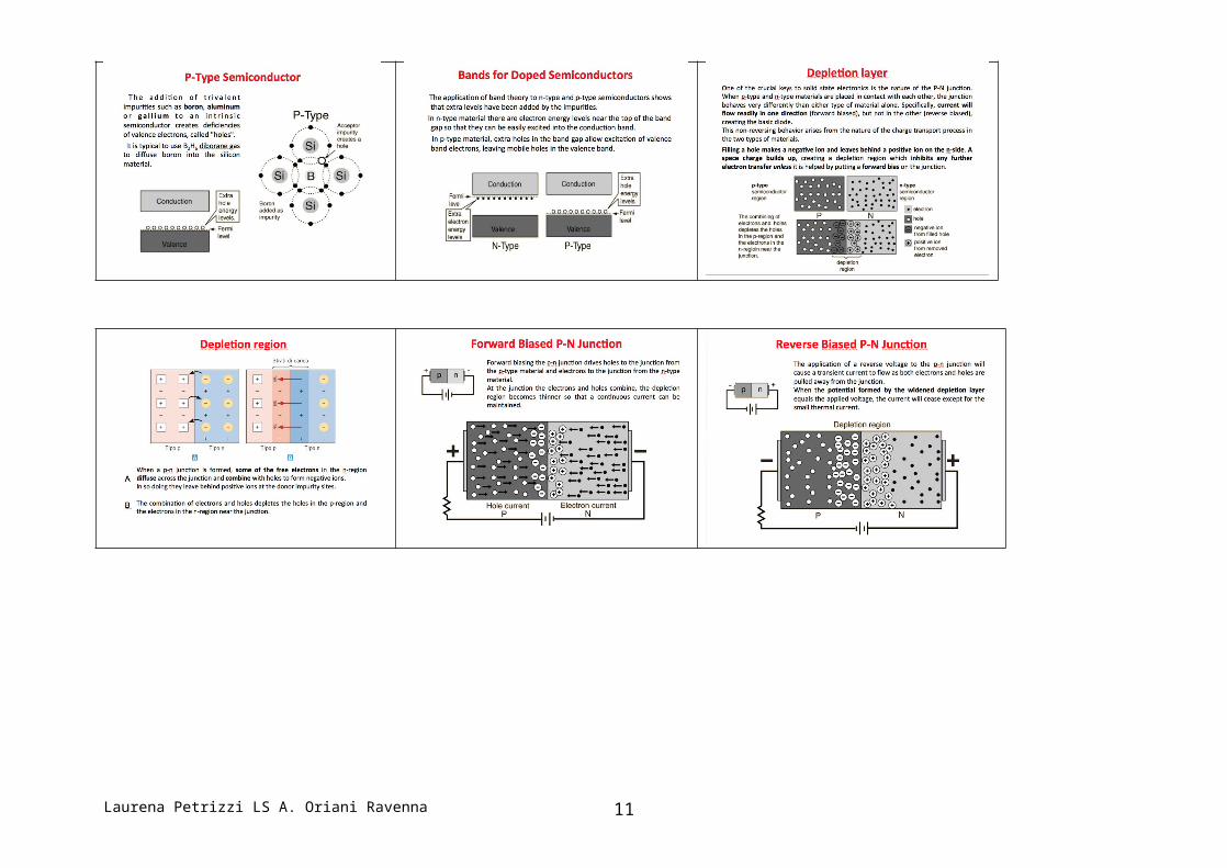
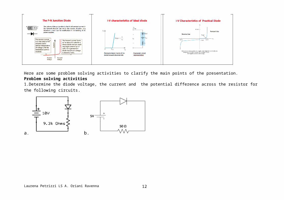
STEP 2. Lecture I from 1 to 24 slideThis step is the first part of the lecture about PN junction. The topics are Band theory of solids, Intrinsic and extrinsic semiconductors, What are P-type and N-type semiconductors, What are Diodes, Forward Bias & Reverse Bias, I – V Characteristics of Ideal Diodes. The lecture is interactive using a Prezi presentation projected on the Lim. I have chosen this software because it is an engaging way to capture the attention of the students and it also gives the possibility to enhance the interactive quality of the lecture. Moreover it is an effective possible tool for them to present their own exam project. During the presentation I am going to put some questions in order to test their attention and comprehension.
Laurena Petrizzi LS A. Oriani Ravenna 7

Laurena Petrizzi LS A. Oriani Ravenna 8

Laurena Petrizzi LS A. Oriani Ravenna 9

Here are some problem solving activities to clarify the main points of the presentation.Problem solving activities1.Determine the diode voltage, the current and the potential difference across the resistor for the following circuits.
a. b.
c.
Laurena Petrizzi LS A. Oriani Ravenna 10
2.Which kind of output do you expect? Try to draw the output voltage across the diode.
Problem solving activities KEY1.Determine the diode voltage, the current and the potential difference across the resistor for the following circuits.
a. (1 mA) b. (86mA)
c. (16mA)
Laurena Petrizzi LS A. Oriani Ravenna 11
2.Which kind of output do you expect? Try to draw the output voltage across the diode.
Solution
STEP 3. a. Video PN junction slide 25This is a revision and consolidation step using a video about PN junction and diodes which helps students to clarify and consolidate some basic points of lecture above.https://youtu.be/W6QUEq0nUH8 (4:07)
STEP 3. b. Crossword activityNow I divide the students into 5 groups of 4 and I assign them tasks and roles. Then I give them copies of the crossword. They have to complete it in 15 minutes. I created the crossword using the free source eclipse crossword.
Laurena Petrizzi LS A. Oriani Ravenna 12

PN junction
Across
3. A voltage applied to a circuit or device, esp a semiconductor device, in the direction that produces the larger current4. To treat a semiconductor with an additive used to improve its properties.5. The difference in energy between electron orbitals in which the electrons are not free to move (called valence bands) and orbitals in which they
are relatively free and can carry a current (called conduction bands).7. Any of various solid crystalline substances, such as germanium or silicon, having electrical conductivity greater than insulators but less than
good conductors, and used especially as a base material for computer chips and other electronic devices.8. A transition region between regions of differing electrical properties in a semiconductor.9. An array of atoms, ions, etc, in a crystal or an array of points indicating their positions in space.10. A vacant position in an atom left by the absence of a valence electron.11. A voltage applied to a circuit or device, esp a semiconductor device, in the direction that blocks the passage of the current.
Laurena Petrizzi LS A. Oriani Ravenna 13

13. A semiconductor which is not doped.14. A machine or tool used for a specific task.Down
1. A region at the interface between dissimilar zones of conductivity in a semiconductor, in which there are few charge carriers.2. The abrupt failure of an insulator or insulating medium to restrict the flow of current.4. An electronic device that restricts current flow chiefly to one direction.6. A nonmetallic element occurring extensively in the earth's crust in silica and silicates and used doped or in combination with other materials in
glass, semiconducting devices.12. To form by combining materials or parts; construct.
Here is the solution to be discussed at the end of the activity.PN junction key
Laurena Petrizzi LS A. Oriani Ravenna 14

Across
3. FORWARDBIAS—A voltage applied to a circuit or device, esp a semiconductor device, in the direction that produces the larger current4. DOPE—To treat a semiconductor with an additive used to improve its properties.5. BANDGAP—The difference in energy between electron orbitals in which the electrons are not free to move (called valence bands) and
orbitals in which they are relatively free and can carry a current (called conduction bands).7. SEMICONDUCTOR—Any of various solid crystalline substances, such as germanium or silicon, having electrical conductivity greater than
insulators but less than good conductors, and used especially as a base material for computer chips and other electronic devices.8. PNJUNCTION—A transition region between regions of differing electrical properties in a semiconductor.9. LATTICE—An array of atoms, ions, etc, in a crystal or an array of points indicating their positions in space.10. HOLE—A vacant position in an atom left by the absence of a valence electron.11. REVERSEBIAS—A voltage applied to a circuit or device, esp a semiconductor device, in the direction that blocks the passage of the current.13. INTRINSIC—A semiconductor which is not doped.14. DEVICE—A machine or tool used for a specific task.
Down
1. DEPLETIONLAYER—A region at the interface between dissimilar zones of conductivity in a semiconductor, in which there are few charge carriers.
2. BREAKDOWN—The abrupt failure of an insulator or insulating medium to restrict the flow of current.4. DIODE—An electronic device that restricts current flow chiefly to one direction.6. SILICON—A nonmetallic element occurring extensively in the earth's crust in silica and silicates and used doped or in combination with other
materials in glass, semiconducting devices.12. BUILDUP—To form by combining materials or parts; construct.
STEP 3. c. FCE activityThe following activities are a FCE reading and comprehension activity part 6, gapped text and a cloze test. The suggested time is 15 minutes each.
FCE Reading- Part 6 –Gapped text
You are going to read an article about PN junction. Seven sentences have been removed from the article. Choose from the sentences A – H the one which fits each gap (1-7). There is one extra sentence you do not need to use.
Laurena Petrizzi LS A. Oriani Ravenna 15

A This energy difference is called a band gap.
B A voltage or current applied to one pair of the transistor's terminals changes the current through another pair of terminals.
C has four valence electrons, each of which participates in a bond in the crystal lattice.
D In doing so, they leave vacancies (holes), which may then be filled by other electrons, thus allowing the electrons to move about the crystal lattice of the material, and a current to flow.
E One can increase the electrical conductivity of a semiconductor by doping it with a small amount of certain other elements
F Thus, doping silicon with a small amount of arsenic produces an n-type semiconductor.
G Most LEDs that have a round case have a longer lead on the anode than on the cathode, and a flat near the cathode lead.
H Such materials are called semiconductors.
PN Junction
The schematic symbol for a diode is:
diode light-emitting diode (LED)
Laurena Petrizzi LS A. Oriani Ravenna 16

As the symbols are oriented above, the wire on the left goes to the anode, and the wire on the right goes to the cathode. (1)…………………How does it work?Materials are often broadly classified as conductors or insulators. For a substance to be a conductor, its electronic structure must be such that there are unoccupied energy levels close enough in energy to where the valence electrons normally reside that the electrons can easily be excited to those levels. (2)………………… These energy levels comprise what is commonly called the conduction band. The levels occupied by the unexcited valence electrons are known as the valence band. In an insulator, the conduction band lies at sufficiently high energy above the valence band that the valence electrons cannot easily reach the levels that lie there, and the material does not conduct electricity. (3)………………… In some materials, the band gap is much smaller than that of an insulator, and the electrical conductivity is intermediate between that of a conductor and that of an insulator. (4)…………………The most commonly used elements in semiconductor devices are probably silicon and germanium. (5)…………………that have either one more or one fewer valence electron than does the semiconductor in question. For example, silicon, which is in qroup IV, (6)…………………. If an arsenic atom, which has five valence electrons, replaces a silicon atom, it then has one electron left over, which cannot participate in bonding and is thus available for conduction. (7)………………… If, instead, one substitutes some boron atoms, which have only three valence electrons, this results in electron vacancies in the crystal lattice, or holes. When an electron moves to fill one of these holes, it leaves behind another hole. This type of semiconductor is called p-type. Thus, we speak of the charge carriers in n-type material as being electrons, and in p-type material as being holes. (Abridged from http://web.physics.ucsb.edu/~lecturedemonstrations/Composer/Pages/64.56)
FCE Open close – Part 2 For questions 1-20, read the text below and think of the word which best fits each gap. Use only one word in each gap.The simplest semiconductor (1)………………... is a p-n junction. That is, a piece of p-type material and a piece of n-type material placed in contact with each other. If no external potential is applied, some of the electrons in the n-type material can cross the junction to fill holes in the p-type material. This leaves a (2)………………... charge on the n-type section and a (3)………………... charge on the p-type section, which prevents further flow of charge carriers across the junction. The resulting potential is (4)………………... the contact potential or junction potential. We will see that we must overcome this junction potential in order to make the diode (5)………………... electricity.If we (6)………………... bias the junction, that is, place a potential across it so that the n-type section is positive with respect to the p-type section, any (7)………………... in the p-type region cross back over the junction into the n-type region, where all the electrons are drawn (8)………………... from the junction towards the positive supply terminal. Similarly, any (9)………………... that were in the n-type region are filled, and the holes in the p-type region are drawn towards the negative terminal. The junction is thus (10)………………... of charge carriers, and current (11)………………... flow.If we bias the junction in the (12)………………... direction, that is, put a potential across it so that the p-type section is now positive with respect to the n-type section, the (13)………………... in the n-type material are repelled from the negative power (14)………………... terminal, as are the holes in the p-type region repelled from the positive terminal. The electrons in the n-type region are drawn towards the (15)………………... , which they can now cross to fill the holes in the p-type region, leaving more holes behind in the n-type region. Current can now (16)………………... , and the diode conducts. Since the above mentioned junction potential is opposite to the forward bias potential, whatever
Laurena Petrizzi LS A. Oriani Ravenna 17

potential we (17)………………... must exceed this junction potential in order for the (18)………………... to conduct. The (19)………………... is, of course, the n-type region, and the (20)………………... is the p-type region.(Abridged from http://web.physics.ucsb.edu/~lecturedemonstrations/Composer/Pages/64.56)
Here is the solution to be discussed at the end of the activity.KEYSFCE Reading- Part 6 –Gapped text
A This energy difference is called a band gap.B A voltage or current applied to one pair of the transistor's terminals changes the current
through another pair of terminals. EXTRAC has four valence electrons, each of which participates in a bond in the crystal lattice.D In doing so, they leave vacancies (holes), which may then be filled by other electrons, thus
allowing the electrons to move about the crystal lattice of the material, and a current to flow.E One can increase the electrical conductivity of a semiconductor by doping it with a small
amount of certain other elementsF Thus, doping silicon with a small amount of arsenic produces an n-type semiconductor.G Most LEDs that have a round case have a longer lead on the anode than on the cathode, and a
flat near the cathode lead.H Such materials are called semiconductors.
FCE Open close – Part 2 The simplest semiconductor device is a p-n junction. That is, a piece of p-type material and a piece of n-type material placed in contact with each other. If no external potential is applied, some of the electrons in the n-type material can cross the junction to fill holes in the p-type material. This leaves a positive charge on the n-type section and a negative charge on the p-type section, which prevents further flow of charge carriers across the junction. The resulting potential is called the contact potential or junction potential. We will see that we must overcome this junction potential in order to make the diode conduct electricity.If we reverse bias the junction, that is, place a potential across it so that the n-type section is positive with respect to the p-type section, any electrons in the p-type region cross back over the junction into the n-type region, where all the electrons are drawn away from the junction towards the positive supply terminal. Similarly, any holes that were in the n-type region are filled, and the holes in the p-type region are drawn towards the negative terminal. The junction is thus depleted of charge carriers, and current cannot flow.If we bias the junction in the forward direction, that is, put a potential across it so that the p-type section is now positive with respect to the n-type section, the electrons in the n-type material are repelled from the negative power supply terminal, as are the holes in the p-type region repelled from the positive terminal. The electrons in the n-type region are drawn towards the junction, which they can now cross to fill the holes in the p-type
Laurena Petrizzi LS A. Oriani Ravenna 18

region, leaving more holes behind in the n-type region. Current can now flow, and the diode conducts. Since the above mentioned junction potential is opposite to the forward bias potential, whatever potential we apply must exceed this junction potential in order for the diode to conduct. The cathode is, of course, the n-type region, and the anode is the p-type region.
STEP 4. Lecture II from 26 to 37 slideThis step is the second part of the lecture about PN junction. The topics are Half wave rectifier with a simple diode, Half wave rectifier with a CR circuit, Full wave rectifier: bridge rectifier, Light emitting diode: LED. The lecture is interactive using a Prezi presentation projected on the Lim. I have chosen this software because it is an engaging way to capture the attention of the students and it also gives the possibility to enhance the interactive quality of the lecture. Moreover it is an effective possible tool for them to present their own exam project. During the presentation I am going to put some questions in order to test their attention and comprehension.
Laurena Petrizzi LS A. Oriani Ravenna 19

STEP 5. Written test I
Laurena Petrizzi LS A. Oriani Ravenna 20

In this phase it is necessary to test the students’ skills and competences. The written test consists of problem solving, fill in, true/false, multiple choice activities.
PHYSICS WRITTEN TEST
Topic: PN junction, diodes Date : ……….
Name: _______________________ Class 5C
Pass 90 points
Multiple choice activity: you are forbidden to erase and change your written choiceMultiple choice + Filling the blanks activities score : 116/1504 points for each right choice 0 point for each wrong choice 1 point for each missing choice Give reasons of the choice if requested, or it is invalidTrue / False activity score:4/1501 point for each right choice0,5 point for each missing choice 0 point for each wrong choiceProblem score: 30/150, see the enclosed rubric
1.When matching polarity connections have been made and the potential difference (PD) is above 0.7 V, the diode is considered to be:A. not workingB. forward biasedC. reverse biasedD. an open switch
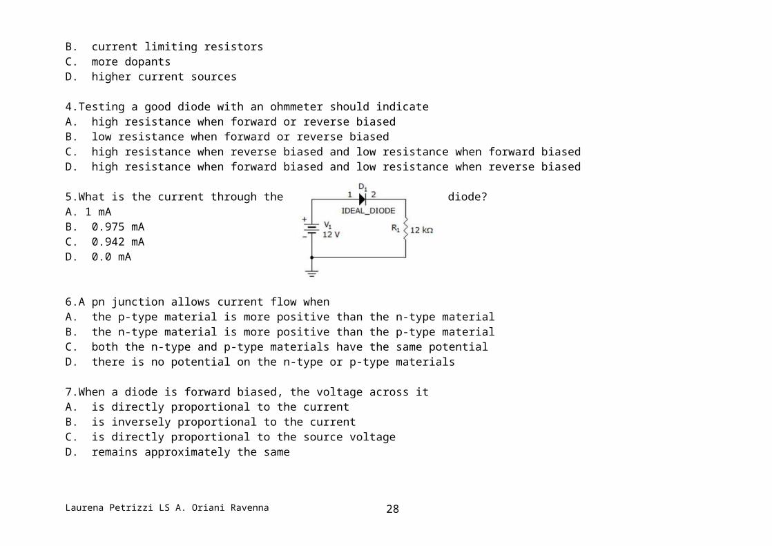
2.What is the current through the LED? A. 0 mAB. 23 mAC. 18 mAD. 13 mA
3.Since diodes are destroyed by excessive current, circuits must have:
Laurena Petrizzi LS A. Oriani Ravenna 21

A. higher voltage sourcesB. current limiting resistorsC. more dopantsD. higher current sources
4.Testing a good diode with an ohmmeter should indicateA. high resistance when forward or reverse biasedB. low resistance when forward or reverse biasedC. high resistance when reverse biased and low resistance when forward biasedD. high resistance when forward biased and low resistance when reverse biased
5.What is the current through the diode?A. 1 mAB. 0.975 mAC. 0.942 mAD. 0.0 mA
6.A pn junction allows current flow whenA. the p-type material is more positive than the n-type materialB. the n-type material is more positive than the p-type materialC. both the n-type and p-type materials have the same potentialD. there is no potential on the n-type or p-type materials
7.When a diode is forward biased, the voltage across itA. is directly proportional to the currentB. is inversely proportional to the currentC. is directly proportional to the source voltageD. remains approximately the same
8.With a 12 V supply, a silicon diode, and a 370-ohm resistor in series, what voltage will be dropped across the diode?A. 0.3 VB. 0.7 VC. 0.9 VD. 1.4 V
Laurena Petrizzi LS A. Oriani Ravenna 22

9. The area at the junction of p-type and n-type materials that has lost its majority carriers is called theA. barrier potentialB. depletion regionC. n regionD. p region
10.DC power should be connected to forward bias a diode as follows:A. – anode, + cathodeB. – cathode, – anodeC. + anode, – cathodeD. + cathode, + anode
11.At any given time in an intrinsic piece of semiconductor material at room temperatureA. electrons drift randomlyB. recombination occursC. holes are createdD. All of the above
12.A reverse biased diode will act as an open switch.A. True B. False
13. If the diode in a series circuit is reverse biased, the resistor will drop all the applied voltage. A.True B. False
14. Reverse biasing a pn junction allows the flow of majority current.A.True B. False
15.Doping semiconductive material is the process of putting a small amount of pentavalent or trivalent atoms in with tetravalent atoms.A.True B. False
16. A ___ is created when an electron moves from the valence band to the conduction band.A. hole B. gap C. vacancy D. blank
17.Typically the forward voltage on an LED is between _______ and ________.
Laurena Petrizzi LS A. Oriani Ravenna 23

A. 1.5 V, 3.7 VB. 0.7 V, 1.1 VC. 1 V, 3 VD. 1 V, 6 V
18.The name of the circuit in the given circuit is the ___.A. half-wave rectifierB. center-tapped full-wave rectifierC. full-wave bridge rectifierD. half-wave bridge rectifier
19.The small amount of ac signal present on the output of a filtering network for a dc power supply is known as ________.A. pulsating dcB. trickleC. rippleD. waffle
20.Atoms in a silicon crystal are held together by ___ bonds.A. crystalB. chemicalC. electricalD. covalent
21.The peak output voltage from the circuit in the given circuit equals ___.A. 3 VB. 3.7 VC. 2.3 VD. 0 V
22.An electron can move to another atom's orbit only while in the _______.A. valence bandB. conduction bandC. orbit nearest the nucleus
Laurena Petrizzi LS A. Oriani Ravenna 24

D. covalent band
23.___ occurs when a pn junction is first formed.A. RecombinationB. Covalent bondingC. CrystallizationD. Breakdown
24.Connecting a capacitor filter to the circuit in the given circuit will___.A. produce a nearly-constant dc voltageB. reduce the output voltageC. increase the ripple voltageD. lower the surge current
25.A pure semiconductor material ___ very well.A. conductsB. insulatesC. conducts and insulatesD. neither conducts nor insulates
26.Single-element semiconductors are characterized by atoms with ____ valence electrons.A. 3B. 4C. 5D. 2
27.Under normal conditions a diode conducts current when it isA. reverse-biased.B. forward-biased.C. avalanched.D. saturated.
28. A diode conducts when it is forward-biased, and the anode is connected to the ________ through a limiting resistor.A. positive supplyB. negative supply
Laurena Petrizzi LS A. Oriani Ravenna 25

C. cathodeD. anode
29.An n-type semiconductor materialA. is intrinsic.B. has trivalent impurity atoms added.C. has pentavalent impurity atoms added.D. requires no doping.
30.The boundary between p-type material and n-type material is calledA. a diode.B. a reverse-biased diode.C. a pn junction.D. a forward-biased diode.
31.What types of impurity atoms are added to increase the number of conduction-band electrons in intrinsic silicon?A. bivalentB. octavalentC. pentavalentD. trivalent
32.Doping of a semiconductor material meansA. that a glue-type substance is added to hold the material together.B. that impurities are added to increase the resistance of the material.C. that impurities are added to decrease the resistance of the material.D. that all impurities are removed to get pure silicon.
33.The forward voltage across a conducting silicon diode is aboutA. 0.3 V.B. 1.7 V.C. –0.7 V.D. 0.7 V.
34.Which lamps are alight? Some may not be full brightness. (30 points)
Laurena Petrizzi LS A. Oriani Ravenna 26

Draw other two circuits, which simulate the behaviour of the circuits above at the best, showing only the lighting lamps. Give reasons for the choice you made.Which are the brightest lamps?
Laurena Petrizzi LS A. Oriani Ravenna 27
IND
ICA
TO
RS
DESCRIPTION OF SKILLS
CO
NT
EN
T
40%
Knowledge of principles, theories, concepts, laws, rules, methods and procedures, scientific terminology
Score 12
Individual score
SOL
UT
ION
ST
RA
TE
GY
40%
Right calculations and reasoning, strategy choice. Accuracy in pictures, schemes, graphic representations and diagrams. Use of notations and scientific means to represent the information.
Score 12
Individual score
LO
GIC
AN
D
INSI
GH
T S
KIL
LS
AN
D
CO
MPE
TE
NC
ES
20%
Organization and use of means, skills and competences aimed at analyzing, dividing into steps, calculating data. Sentence flow, sentence structure and grammar, terminology used. Coherence and cohesion in the insight.
Score 6
Individual score
PHYSICS WRITTEN TEST KEY
Topic: PN junction, diodes Date : ……….
Name: _______________________ Class 5C
Laurena Petrizzi LS A. Oriani Ravenna 28

Pass 90 points
Multiple choice activity: you are forbidden to erase and change your written choiceMultiple choice + Filling the blanks activities score : 116/1504 points for each right choice 0 point for each wrong choice 1 point for each missing choice Give reasons of the choice if requested, or it is invalidTrue / False activity score:4/1501 point for each right choice0,5 point for each missing choice 0 point for each wrong choiceProblem score: 30/150, see the enclosed rubric
1.When matching polarity connections have been made and the potential difference (PD) is above 0.7 V, the diode is considered to be:A. not workingB. forward biasedC. reverse biasedD. an open switch
2.What is the current through the LED?A. 0 mAB. 23 mAC. 18 mAD. 13 mA
3.Since diodes are destroyed by excessive current, circuits must have:A. higher voltage sourcesB. current limiting resistorsC. more dopantsD. higher current sources
4.Testing a good diode with an ohmmeter should indicateA. high resistance when forward or reverse biased
Laurena Petrizzi LS A. Oriani Ravenna 29

B. low resistance when forward or reverse biasedC. high resistance when reverse biased and low resistance when forward biasedD. high resistance when forward biased and low resistance when reverse biased
5.What is the current through the diode?A. 1 mAB. 0.975 mAC. 0.942 mAD. 0.0 mA
6.A pn junction allows current flow whenA. the p-type material is more positive than the n-type materialB. the n-type material is more positive than the p-type materialC. both the n-type and p-type materials have the same potentialD. there is no potential on the n-type or p-type materials
7.When a diode is forward biased, the voltage across itA. is directly proportional to the currentB. is inversely proportional to the currentC. is directly proportional to the source voltageD. remains approximately the same
8.With a 12 V supply, a silicon diode, and a 370-ohm resistor in series, what voltage will be dropped across the diode?A. 0.3 VB. 0.7 VC. 0.9 VD. 1.4 V
9. The area at the junction of p-type and n-type materials that has lost its majority carriers is called theA. barrier potentialB. depletion regionC. n regionD. p region
10.DC power should be connected to forward bias a diode as follows:
Laurena Petrizzi LS A. Oriani Ravenna 30

A. – anode, + cathodeB. – cathode, – anodeC. + anode, – cathodeD. + cathode, + anode
11.At any given time in an intrinsic piece of semiconductor material at room temperatureA. electrons drift randomlyB. recombination occursC. holes are createdD. All of the above
12.A reverse biased diode will act as an open switch.A. True B. False
13.If the diode in a series circuit is reverse biased, the resistor will drop all the applied voltage.A.True B. False
14. Reverse biasing a pn junction allows the flow of majority current.A.True B. False
15.Doping semiconductive material is the process of putting a small amount of pentavalent or trivalent atoms in with tetravalent atoms.A.True B. False
16. A ___ is created when an electron moves from the valence band to the conduction band.A. hole B. gap C. vacancy D. blank
17.Typically the forward voltage on an LED is between _______ and ________.A. 1.5 V, 3.7 VB. 0.7 V, 1.1 VC. 1 V, 3 VD. 1 V, 6 V
18.The name of the circuit in the given circuit is the___.A. half-wave rectifierB. center-tapped full-wave rectifier
Laurena Petrizzi LS A. Oriani Ravenna 31

C. full-wave bridge rectifierD. half-wave bridge rectifier
19.The small amount of ac signal present on the output of a filtering network for a dc power supply is known as ________.A. pulsating dcB. trickleC. rippleD. waffle
20.Atoms in a silicon crystal are held together by ___ bonds.A. crystalB. chemicalC. electricalD. covalent
21.The peak output voltage from the circuit in the given circuit equals ___.A. 3 VB. 3.7 VC. 2.3 VD. 0 V
22.An electron can move to another atom's orbit only while in the _______.A. valence bandB. conduction bandC. orbit nearest the nucleusD. covalent band
23.___ occurs when a pn junction is first formed.A. RecombinationB. Covalent bondingC. CrystallizationD. Breakdown
Laurena Petrizzi LS A. Oriani Ravenna 32

24.Connecting a capacitor filter to the circuit in the given circuit will___.A. produce a nearly-constant dc voltageB. reduce the output voltageC. increase the ripple voltageD. lower the surge current
25.A pure semiconductor material ___ very well.A. conductsB. insulatesC. conducts and insulatesD. neither conducts nor insulates
26.Single-element semiconductors are characterized by atoms with ____ valence electrons.A. 3B. 4C. 5D. 2
27.Under normal conditions a diode conducts current when it isA. reverse-biased.B. forward-biased.C. avalanched.D. saturated.
28. A diode conducts when it is forward-biased, and the anode is connected to the ________ through a limiting resistor.A. positive supplyB. negative supplyC. cathodeD. anode
29.An n-type semiconductor materialA. is intrinsic.B. has trivalent impurity atoms added.
Laurena Petrizzi LS A. Oriani Ravenna 33

C. has pentavalent impurity atoms added.D. requires no doping.
30.The boundary between p-type material and n-type material is calledA. a diode.B. a reverse-biased diode.C. a pn junction.D. a forward-biased diode.
31.What types of impurity atoms are added to increase the number of conduction-band electrons in intrinsic silicon?A. bivalentB. octavalentC. pentavalentD. trivalent
32.Doping of a semiconductor material meansA. that a glue-type substance is added to hold the material together.B. that impurities are added to increase the resistance of the material.C. that impurities are added to decrease the resistance of the material.D. that all impurities are removed to get pure silicon.
33.The forward voltage across a conducting silicon diode is aboutA. 0.3 V.B. 1.7 V.C. –0.7 V.D. 0.7 V.
34.Which lamps are alight? Some may not be full brightness. (30 points)
Laurena Petrizzi LS A. Oriani Ravenna 34

Draw other two circuits, which simulate the behaviour of the circuits above at the best, showing only the lighting lamps. Give reasons for the choice you made.Which are the brightest lamps?
Laurena Petrizzi LS A. Oriani Ravenna 35

STEP 6. a. Video Transistors slide 38This step engages the students to go deep into the topic using their own skills and competences to find out further information about other electronic components. They will be able to do it using video about transistors and a webquest activity in the IT lab.https://youtu.be/FODFowmDfvY (6:29)To start the webquest the students are given a problem through questions:What is a transistor? Can you trace a brief history of transistors? How many kinds of transistor are available?How are transistors made?What are the functions of a transistor?The suggested sources for the webquest are: http://www.bbc.co.uk/schools/gcsebitesize/design/electronics/switchesrev3.shtmlhttps://en.wikipedia.org/wiki/Transistorhttp://www.nobelprize.org/educational/physics/transistor/function/index.htmlhttps://en.wikibooks.org/wiki/Semiconductors/Introduce_to_Transistorhttps://www.youtube.com/watch?v=FODFowmDfvYhttps://www.youtube.com/watch?v=CkX8SkTgB0ghttps://www.youtube.com/watch?v=4QkRI1Ue208https://www.youtube.com/watch?v=SjeK1nkiFvIhttps://www.youtube.com/watch?v=W6QUEq0nUH8
They are also given the following task:Create a presentation in PREZI, PPT, KEYNOTE, etc. following the outline above.Specify the sources used following the hints from http://www.unive.it/nqcontent.cfm?a_id=39026The students have a week to complete the work.I enclose the rubric for the assessment of the oral presentation.
Laurena Petrizzi LS A. Oriani Ravenna 36

Rubric - Presenter Skills and Attributes in Scientific Oral Presentation
Laurena Petrizzi LS A. Oriani Ravenna 37

Further written test Problem solving for the simulation of Terza Prova
Laurena Petrizzi LS A. Oriani Ravenna 38
INDICATORS DESCRIPTION OF SKILLS – ATTRIBUTES – COMPETENCES SCORE Individual score
ORGANIZATION-PLANNING Planning Use of schemes, diagrams, maps Slide order
Very poor/poor planning skills, competences Acceptable/passing planning skills, competences Adequate planning skills, competences Good/Excellent planning skills, competences
0.5 1 1.5 2
ACCURACY Slide numbers Date Footer Bibliography/sources/references
Poor/partly adequate accuracy Adequate accuracy Good/Excellent accuracy
0.5 1 1.5
CONTENT Understanding of theme and
relationship to topic Use of supporting examples or
details Organization, sentence structure
and grammar Appropriate use of terminology
(scientific vocabulary) Pronunciation Synthesis
Poor/confused organization, grammatical, spelling and pronunciation errors, difficulty in expressing ideas and information, recurrent hesitations, incorrect terminology, very poor, understanding of theme, lacking or incorrect examples/details
Acceptable/passing, some organizational and grammatical problems, passing use of terminology and pronunciation, evidence of limited understanding, minimal examples and details
Adequate, minimal errors and mistakes, adequate terminology and pronunciation, evidence of a basic understanding and synthesis, adequate supporting examples and/or details
Good sentence flow, sentence structure and grammar, good pronunciation, terminology correctly used, evidence of good understanding and synthesis, examples or/and details generally well applied to theme
Very good/Excellent, excellent organization, sentence structure and grammar, accurate scientific terminology, very good pronunciation, evidence of full and complete understanding, well chosen examples, accurate details applied to theme
1.5 2.5
3 4
5
ICT Use of the chosen software Graphic design Graphics/use of images Hyperlinks/Links Use of transitions and animations
Poor/Adequate technical skills and competences Adequate technical skills and competences Good/Excellent technical skills and competences
0.5 1 1.5
Totale:GIUDIZIO Insuff. molto
grave-impreparatoInsuff. grave con mancato raggiungimento degli obiettivi minimi
Insuff. non grave con parziale raggiungimento degli obiettivi
Sufficiente Discreto Buono Ottimo/Eccellente
Voto in 1/10 1 - 3 4 - 4.5 5 - 5.5 6 6.5 - 7 7.5 - 8.5 9 - 10

1) What do you mean by N-type and P-type semiconductors and what is the most important difference between an intrinsic and an extrinsic semiconductor? What happens when you make a PN junction? When do you have a forward bias or a reverse bias connection?
a.Can you identify which diode is conducting in this circuit and can you explain why?
or b.Assuming D1 and D2 are ideal diodes. What is the current flowing in the diode D2 and what is the potential difference across the same diode?
2) Can you draw the peak rectifier circuit using a diode with CR filter and can you briefly describe and explain how it works?
3) With reference to its volt ampere characteristic, can you explain how a silicon diode can be used to rectify a double-wave signal into a half-wave signal?
Further oral test
Laurena Petrizzi LS A. Oriani Ravenna 39

INDICATORS DESCRIPTION OF SKILLS – ATTRIBUTES – COMPETENCES SCORE Individual scoreCoherence-CohesionDiscourse management
Coherence, cohesion and fluency Discourse management
Lack of cohesion and coherence, difficult communication often teacher-led, inadequate discourse management Adequate discourse managementExcellent fluency and discourse management
0.51
1.5Grammar, vocabulary, pronunciation
Organization, sentence structure and grammar Appropriate use of terminology Pronunciation
Poor organization grammatical, spelling and pronunciation errors, difficulty in expressing ideas and information, recurrent hesitations, incorrect terminologySome organizational and grammatical problems, adequate terminology and pronunciationGood sentence flow, sentence structure and grammar, good pronunciation, terminology correctly used Excellent organization, sentence structure and grammar, accurate scientific terminology, very good pronunciation
0.5
1
1.5
2Content
Understanding of theme and relationship to topic Use of supporting examples or details Synthesis
Very poor, no understanding of theme, lacking or incorrect examples/detailsPoor, evidence of limited understanding, minimal examples and details Adequate, evidence of a basic understanding and synthesis, adequate supporting examples and/or detailsGood, evidence of good understanding and synthesis, examples or/and details generally well applied to theme Excellent, evidence of full and complete understanding, well chosen examples, accurate details applied to theme
1.52
3
4
4.5
Interactive communication Interaction Communicative skills
Difficult interaction among the students and between a student and the teacher Adequate interaction but essential and simple Good interaction among the speakers without any interruption and in turn Excellent interaction and discourse organization
0.5
1
1.52
Assessment Totale:GIUDIZIO Insuff. , molto
grave-impreparatoInsuff. , grave con mancato raggiungimento degli obiettivi minimi
Insuff. non grave con parziale raggiungimento degli obiettivi
Sufficiente Discreto Buono Ottimo/Eccellente
Voto in 1/10 1 - 3 4 - 4.5 5 - 5.5 6 6.5 - 7 7.5 -8.5 9 - 10
Laurena Petrizzi LS A. Oriani Ravenna 40