Embed Size (px)
Citation preview

Dynamic Resolution Control in a Laser Projection based
Stereolithography System
Yayue Pan*, Chintan Dagli
Department of Mechanical and Industrial Engineering, University of Illinois at Chicago, Chicago, IL
60607
* Corresponding author: [email protected], (312)996-8777
Abstract
In a typical Additive Manufacturing system, it is critical to make a trade-off between the
resolution and build area for applications in which varied dimensional sizes, feature sizes, and
accuracies are desired. The lack of the capability in adjusting resolution dynamically during
building processes limits the use of AM in fabricating complex structures with big layer areas
and small features. In this paper, a novel AM system with dynamic resolution control by
integrating a laser projection in vat photopolymerization process is presented. Theoretical models
and parameter characterizations are presented for the developed AM system. Accordingly, the
process planning and mask image planning approaches for fabricating models with varied
dimensional sizes and feature sizes have been developed. Multiple test cases based on various
types of structures have been performed.
Keywords: Additive Manufacturing, vat photopolymerization, Stereolithography, Resolution Control,
Build Size
1. Introduction
1.1 Backgrounds and motivations
Additive Manufacturing (AM), often referred to as Solid Freeform Fabrication (SFF) or 3D
Printing or Rapid Prototyping, is a class of technologies that can fabricate parts with almost any
freeform geometries directly from three-dimensional computer aided models by accumulating
material together, usually in a layer by layer manner.
In past decades, intensive research attempts have been made to improve the performance of
AM systems, in terms of build speed [1, 2], surface quality [3-5], material property[6-8], process
reliability [7], etc. This technology finds its applications as a rapid prototyping technology in a
wide variety of fields such as architecture, construction, industrial design, automotive, aerospace,
military, engineering, medical, biotech, fashion, footwear, jewelry and education [9-11].
However, many limitations still exist in AM and hinder its application in fabricating end-use
products, including size and resolution limitations, imperfections, limited choices of materials,
low through-put, etc. [12]. In this research, we focus on working to overcome one of its primary
243

drawbacks: size and resolution limitations, in a Stereolithography related AM system which has
entered the mainstream of 3D printing industry.
Stereolithography (SL) related AM technology can achieve a wide range of resolutions. As of
today, various commercial machines have successfully entered the market, typically offering
resolutions in the range of 20µm ~200µm and build envelope diagonal size of 30 ~ 500 mm.
There are two types of Stereolithography related AM technologies: laser scanning based, and
projection based technologies. In the early stage, laser beam is used in SL system to cure liquid
resin path by path to form one layer. With the advancement in Micro-Electro-Mechanical
Systems (MEMS), projection based SL process becomes a more popular SL related AM
technology these years due to their dynamic mask generation capability. In a projection SL
system, a digital micromirror device (DMD) is usually used to pattern the light. A DMD is a
Micro-Electro-Mechanical Systems device that enables one to simultaneously control small
mirrors that turn on or off a pixel at over 5 KHz. Using this technology, a light projection device
can project a dynamically defined mask image onto a resin surface to selectively cure liquid resin
into layers of the object. Consequently, the related AM process, Mask Image Projection
Stereolithography (MIP-SL), can be much faster than the laser based SL process by
simultaneously forming the shape of a whole layer, and can achieve a much higher resolution by
having a big number of micro-mirrors and focusing each pixel in a small area. Many research
groups demonstrated micro-manufacturing capability with micron or even sub-micron scale
resolution in MIP-SL systems [3, 5, 13-15].
Despite the advancement of SL related AM technologies, conflict between the build size and
resolution is a historically inherent manufacturing dilemma. In order to achieve higher
resolution, a smaller laser beam spot or a smaller pixel size is desired, in turn, a smaller build
size will be created. Due to the fundamental energy distribution mechanism in SL related AM
technologies, build size and resolution have always been two conflicting goals. Recently a
method to solve this dilemma by projecting multiple images in different areas to make one big
layer is proposed by Emami et. al [16]. However this approach will lengthen the build time
greatly and make the process much more complicated.
The thrust of this research is to contribute to the advancement of AM by addressing such a
dilemma of the resolution and build size, without affecting other manufacturing performance
factors like build speed and process reliability. To achieve this goal, a continuous resolution
control approach is investigated by using a laser projection technology.
1.2 Novelty and Contributions
A schematic diagram of the conventional MIP-SL process is represented in Fig. 1a. A lamp is
usually used as a light source and a DMD chip is used to pattern the light. Optical lens is used to
focus the patterned light onto a liquid resin surface. In a system, the resolution is determined by
the lens' focal length and fixed. To cure a layer with different area, different number of pixels
244
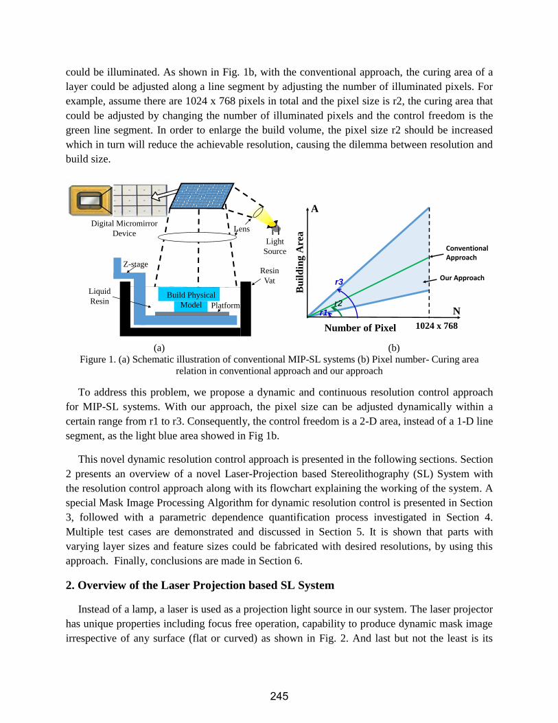
could be illuminated. As shown in Fig. 1b, with the conventional approach, the curing area of a
layer could be adjusted along a line segment by adjusting the number of illuminated pixels. For
example, assume there are 1024 x 768 pixels in total and the pixel size is r2, the curing area that
could be adjusted by changing the number of illuminated pixels and the control freedom is the
green line segment. In order to enlarge the build volume, the pixel size r2 should be increased
which in turn will reduce the achievable resolution, causing the dilemma between resolution and
build size.
(a) (b)
Figure 1. (a) Schematic illustration of conventional MIP-SL systems (b) Pixel number- Curing area
relation in conventional approach and our approach
To address this problem, we propose a dynamic and continuous resolution control approach
for MIP-SL systems. With our approach, the pixel size can be adjusted dynamically within a
certain range from r1 to r3. Consequently, the control freedom is a 2-D area, instead of a 1-D line
segment, as the light blue area showed in Fig 1b.
This novel dynamic resolution control approach is presented in the following sections. Section
2 presents an overview of a novel Laser-Projection based Stereolithography (SL) System with
the resolution control approach along with its flowchart explaining the working of the system. A
special Mask Image Processing Algorithm for dynamic resolution control is presented in Section
3, followed with a parametric dependence quantification process investigated in Section 4.
Multiple test cases are demonstrated and discussed in Section 5. It is shown that parts with
varying layer sizes and feature sizes could be fabricated with desired resolutions, by using this
approach. Finally, conclusions are made in Section 6.
2. Overview of the Laser Projection based SL System
Instead of a lamp, a laser is used as a projection light source in our system. The laser projector
has unique properties including focus free operation, capability to produce dynamic mask image
irrespective of any surface (flat or curved) as shown in Fig. 2. And last but not the least is its
Light
Source
Lens
Resin
Vat
Build Physical
Model
Liquid
Resin
Z-stage
Platform
Digital Micromirror
Device
Conventional Approach
Bu
ild
ing
Are
a
Number of Pixel
N
A
1024 x 768
r1
r3
r2
Our Approach
245

compact size that makes it easy to be adopted and integrated into the additive manufacturing
system. These unique characteristics of laser projector eventually provide a distinct capability to
change the projection image size and resolution easily.
The laser projector is composed of three LEDs (blue, red and green) and a MEMS scanner.
The projected image is created by modulating the three lasers synchronously with the position of
the scanned beam [17]. The projected beam directly leaves the MEMS scanner and creates a
sharp image irrespective of any surface (flat or curved) it is shone upon [17].
(a) (b)
Figure 2. Laser Projector unique properties: (a) Stays focus when changing focal length; (b) Project on
any shape surface
(a) (b)
Figure 3. (a) A Laser Projection based SL system with dynamic resolution control (b) Flowchart of the
working of Laser Projection based SL system
The Laser Projection based SL system design is shown in Fig. 3a above and the flowchart in
Fig. 3b explains the working of the entire system. Similar to the conventional approach, we start
from a CAD model. However, instead of slicing the STL file with a certain predefined
resolution setting, we first analyze feature sizes of the CAD model, and then set a resolution for
each layer. After that, mask images will be generated by slicing each layer with the desired
resolution setting. These mask images are then transferred to the laser projector for layer by layer
fabrication. The laser projector then moves to a corresponding position to cure that layer with the
(a) (b)
Sliced STL Files
Part
Platform
PDMS layer
Resin
X, Y, Z-stage 1
Resin Vat
Z-stage 2
Motion Controller
MEMS Scanner
Red LD
Blue LD
Green SHG
Motion Controller
Yes
CAD Model
Generate sliced images with desired resolution settings
Transfer 2D sliced image to laser projector
Translate laser projector up and down to gain the
required resolution settings
Project the mask image onto the Liquid Resin
Last Layer?
Pull out Fabricated Part
No
Analyze Feature sizes and plan a set of resolutions
for each layer
246

desired resolution and simultaneously the pixel size changes dynamically according to the
position of laser projector. Therefore, in this dynamic resolution control manufacturing process
the above two steps highlighted in blue are the most important. Correspondingly, two
fundamental research questions need to be answered:
1. How to determine a proper set of resolutions for each layer to achieve best part quality.
2. How to move projector to the proper position to gain the required resolution.
Question 1 will be answered in Section 3 by exploring an image processing algorithm to filter
features with different resolution requirements. Question 2 will be investigated in Section 4 by
quantifying the parametric dependence of resolution and build size on manufacturing process
parameters.
3. Image Processing Algorithm
It is therefore very essential to answer the first question about how to determine proper
resolution for each layer so as to obtain best quality part and therefore we proposed an image
processing algorithm to answer this question. For instance, a solid freeform fabrication design
model is sliced into a set of layers and it might have micro-scale and a macro-scale features in a
single layer. If this layer is fabricated with a proper resolution corresponding to the macro-scale
feature, the micro feature could not be fabricated out due to the insufficient resolution. However,
if a high resolution setting is used to give the required accuracy for fabricating micro features,
the build size may not be big enough to fabricate out the whole layer. Therefore, for each sliced
layer, a proper resolution or a proper set of resolutions need to be determined to achieve the
desired accuracy and build size for that layer without sacrificing the other manufacturing
performances like build speed.
In this study, a single Layered Depth Image (LDI) algorithm is utilized to determine the
proper set of resolutions for each layer. LDI is generally used for 2-dimensional images which
can be extended further to Layered Depth-Normal Images commonly known as LDNI [18]. In
the following sections, for easy understanding, we use "micro feature" or "micro image" to
denote an area which has to use a high resolution R1 to fabricate, and "macro feature" or "macro
image" to denote an area which could use a low resolution R2 to fabricate.
The following example Fig. 4 illustrates a simple sliced binary image for a single layer that
contains micro feature in a large area. We segmented the micro features from the macro part so
as to build these small features with higher resolution in order to highlight its intricate details.
Let V comprises of the entire image having i pixels along X-direction and j-pixels along Y-
direction. Originally, the image is sliced by using the lowest resolution setting in our system,
which is 81 microns per pixel denoted as R81. This can be represented as (Xi, Yj) ∈ V for a single
layer that can be extended to the 3rd dimension identifying the Kth sliced layer. Thus the overall
equation can be represented as (Xi, Yj) ∈ VLayer_K. In order to filter the micro feature which cannot
247

be fabricated by using the lowest resolution R81, rays are transmitted along each row pixel first
and then each column pixel. We consider each row as a separate image and run the loop. When
the ray identifies a pixel that has its neighboring pixel of different intensity it shall be marked as
the boundary of the object.
In the following example, a sectional part is highlighted to show the working of the algorithm.
The system identifies the object pixel and mark the boundary pixel at the respective position as
Xi,n, where n is the change in the pixel intensity ranges from 0 to infinity. The ray starts with n
value as 0 and changes to 1 immediately when it finds the 1st boundary pixel and then proceeds
with an increment when it encounters discontinuity. Thus, the next boundary will have Xi+p,n+1,
where p is any arbitrary value of X position. The distance between any two boundaries of an
object can be generalized as d|Xi+p,n_even- Xi,(n_even)-1|, except when n is 0. We set a threshold value
T for the pixel distance which indicates that if the distance between two boundary object pixel
exceeds the threshold it will be counted as meso-scale or macro-scale feature, whereas if the
distance between the boundary object pixel is less than the threshold it will be counted as the
micro-scale feature which cannot be fabricated by using resolution R81 and the object pixel will
be marked as 0.
Figure 4. Example Model (a) STL Model; (b) Transfer Rays along Rows and Columns of a Binary Sliced
Layered Image; (c) Sectional View highlighting object and boundary detection; (d) Macro Image; (e)
Micro Image
For example, in the sectional image in Fig. 4, the ray transmitted along the row starts with n as
0 and then ends with n as 6, thus the row has 6 boundaries and 3 objects. It is identified that the
d|X15,2 – X5,1| and d|X59,6 – X49,5| is greater than the threshold T, thus identified as macro image.
On the contrary, the other object is micro image since the d| X35,4 – X29,3| is less than T. After
X
YX0,0
X5,1 X15,2 X29,3X35,4 X49,5
X59,6
(a) (b)
(d) (e)
(c)
248

identifying the micro-scale features, it will set all micro pixel object area to zero, we run the loop
for all the rows and then a new image is generated. For better efficiency we then run this loop for
all the columns on the new image and again the identified micro objects are set zero forming a
modified image. The modified image thus obtained is the macro image and subtracting this
modified image from the initial image will give out a micro image. Then the macro image is used
for fabricating the related part by using R81. The micro features separated from the original
sliced image, a higher resolution R81- (denoting a resolution of 81- microns per pixel) is
used to regenerate an image for the micro features. Then the regenerated image is used as the
input image and is processed the same way to determine a proper resolution for it. Following
algorithm provides a throughout understanding of the working of image processing approach. R#
means a resolution of # microns per pixel.
Algorithm1:
INPUT
A binary image sliced by using R#, V of Kth layer.
OUTPUT
1. Macro Image
2. Micro Image
STEPS
1. Transfer rays from Yj till Yj+w, where j=0 w and w = number of pixels along Y-axis
2. For each row find boundary pixel, Xi,n, where i=0 v and v= number of pixels along X-
axis and n= change in pixel intensity
3. If d|Xi+p,n_even- Xi,(n_even)-1|≥ T, macro image else micro-image
4. If d|Xi+p,n_even- Xi,(n_even)-1|<T, set d|Xi+p,n_even- Xi,(n_even)-1|=0
5. New image as V_row
6. Repeat above steps for column rays on V_row
7. Store the modified image V_mac
8. V_mic =V - V_mac
RESULT
V_mac as macro image which will be used to fabricate a part of that layer using resolution R#
V_mic as micro image which the resolution needs to be updated.
4. Parametric Dependence Quantification
After obtaining the desired resolutions for each layer using Image Processing Algorithm, the
next thing is to move the laser projector to the corresponding position to fabricate that part of
that layer with its desired resolution. This is quantified by the dependence of pixel size and build
size on the focal length. By moving the laser projector up and down using Z-stage 2 as shown in
Fig. 3a, the digital mask images exposed on the liquid resin would have changing resolution and
build size. More specifically if the laser projector is moved away from the platform the pixel size
increases which means lower resolution but bigger build area. For example, the micro scale
249

structures could be segmented and fabricated with a small focal length and hence higher
resolution, while the meso-scale structures in the model could be fabricated with a bigger focal
length and hence larger curing area. The following section shows the relationship between pixel
size and build size on the focal length.
4.1 Quantifying Parametric Dependence of: Build Area & Resolution on Focal Length
Due to the laser property of producing focus free masks irrespective of any focal distance, it
provides a wide variety of resolution depending upon its distance from the bottom surface of
resin vat. Thus, a process planning approach is essential for determining the position of the
projector to obtain the required resolution for each layer. Both the resolution and building area
are related to the focal length and there exist a linear co-relationship which has been highlighted
in the following Fig. 5. The graph highlighted in red is related to the focal length and the
resolution (y-axis on the right termed as 𝑦2) it produces whereas the graphs in blue (dashed line)
and orange (round dotted line) are associated to the focal length and building sizes (y axis on the
left termed as 𝑦1) along X and Y-axis respectively. The linear relationship between focal length x
and building area y could be formulated as the following:
𝑦1 = 0.8 ∗ 𝑥 + 14.1333 along X-axis
𝑦1 = 0.8 ∗ 𝑥 + 14.1333 along Y-axis
whereas, Focal Length x (mm) and Planar Resolution y (micron/pixel) could be described by:
𝑦2 = 0.9906 ∗ 𝑥 + 16.6597
From the above equations, it's obvious that for producing parts with high resolution the focal
distance between the laser projector and resin vat should be small and conversely for the
development of parts with large area its focal distance will be large. Given a desired resolution,
the projector could be moved to the corresponding position. Also, the fabrication of one layer
with large area but small features, the mask image could be segmented into multiple images for
multiple curing with different projector positions. As shown in Fig. 5, the projector provides a
good flexibility with a building area of 73.0 mm to 31.0 mm along X-axis and 41.32 mm to
17.54 mm along Y-axis subject to the focal length of 70.0 mm to 20.0 mm respectively.
Correspondingly, its resolution varies from 86.08 micron/pixel to 36.55 micron/pixel.
250
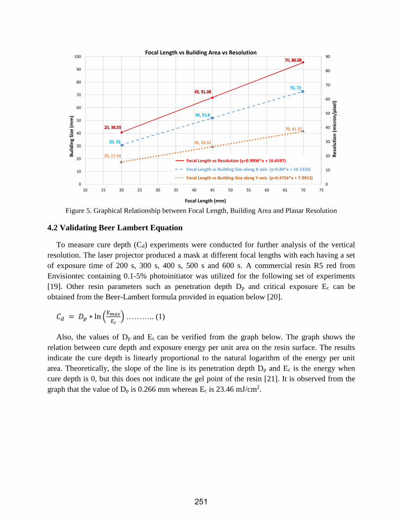
Figure 5. Graphical Relationship between Focal Length, Building Area and Planar Resolution
4.2 Validating Beer Lambert Equation
To measure cure depth (Cd) experiments were conducted for further analysis of the vertical
resolution. The laser projector produced a mask at different focal lengths with each having a set
of exposure time of 200 s, 300 s, 400 s, 500 s and 600 s. A commercial resin R5 red from
Envisiontec containing 0.1-5% photoinitiator was utilized for the following set of experiments
[19]. Other resin parameters such as penetration depth Dp and critical exposure Ec can be
obtained from the Beer-Lambert formula provided in equation below [20].
𝐶𝑑 = 𝐷𝑝 ∗ ln (𝐸𝑚𝑎𝑥
𝐸𝑐) ……….. (1)
Also, the values of Dp and Ec can be verified from the graph below. The graph shows the
relation between cure depth and exposure energy per unit area on the resin surface. The results
indicate the cure depth is linearly proportional to the natural logarithm of the energy per unit
area. Theoretically, the slope of the line is its penetration depth Dp and Ec is the energy when
cure depth is 0, but this does not indicate the gel point of the resin [21]. It is observed from the
graph that the value of Dp is 0.266 mm whereas Ec is 23.46 mJ/cm2.
0
10
20
30
40
50
60
70
80
90
0
10
20
30
40
50
60
70
80
90
100
10 15 20 25 30 35 40 45 50 55 60 65 70 75
Focal Length vs Building Area vs Resolution
Focal Length vs Resolution (y=0.9906*x + 16.6597)
Focal Length vs Building Size along X-axis (y=0.84*x + 14.1333)
Focal Length vs Building Size along Y-axis (y=0.4756*x + 7.9913)
Focal Length (mm)
Bu
ildin
g Si
ze (
mm
)
Re
solu
tio
n (
mic
ron
/pix
el)
251

Figure 6. Graphical Relationship between Exposure Energy and Cure Depth
4.2.1 Dependence of Cure Depth on Focal Length
On further extending Beer Lambert equation the relationship between the cure depth and focal
length has been established using equation 1, as represented below:
𝐶𝑑 = 𝐷𝑝 ∗ ln (𝐸𝑚𝑎𝑥
𝐸𝑐)
𝐶𝑑 = 𝐷𝑝 ∗ ln (𝑃𝑚𝑎𝑥 ∗𝑇
𝐴∗𝐸𝑐)………. (2)
where, Pmax = Laser Power, T= time, A= cured area.
Since all the variables in equation 2 are constant for a specific time and also the cured area is
directly proportional to the focal length d, the above equation can be represented as follows:
𝐶𝑑 = 𝐷𝑝 ∗ 𝑙𝑛 (𝐾𝑐𝑜𝑛𝑠𝑡𝑎𝑛𝑡
𝑑)
𝐶𝑑 = 𝐷𝑝 ∗ ln(𝐾𝑐𝑜𝑛𝑠𝑡𝑎𝑛𝑡) − 𝐷𝑝 ∗ ln(𝑑)
𝐶𝑑 = 𝐾′𝑐𝑜𝑛𝑠𝑡𝑎𝑛𝑡 − 𝐷𝑝 ∗ ln(𝑑) ……… (3)
Equation 3 can be validated with the graph below that justifies the relation between cure depth
and focal length. These linear equations in Fig. 7 are obtained when the laser projector produce
slice image on the build surface for a specified time under different focal length.
0
0.1
0.2
0.3
0.4
0.5
0.6
0.7
0.8
0.9
2.75 3 3.25 3.5 3.75 4 4.25 4.5 4.75 5 5.25 5.5 5.75 6 6.25 6.5
Cu
re D
epth
, C
d (m
m)
Natural Logarithm of Exposure Energy, Emax (mJ/cm2)
Cure Depth vs Exposure Energy
252
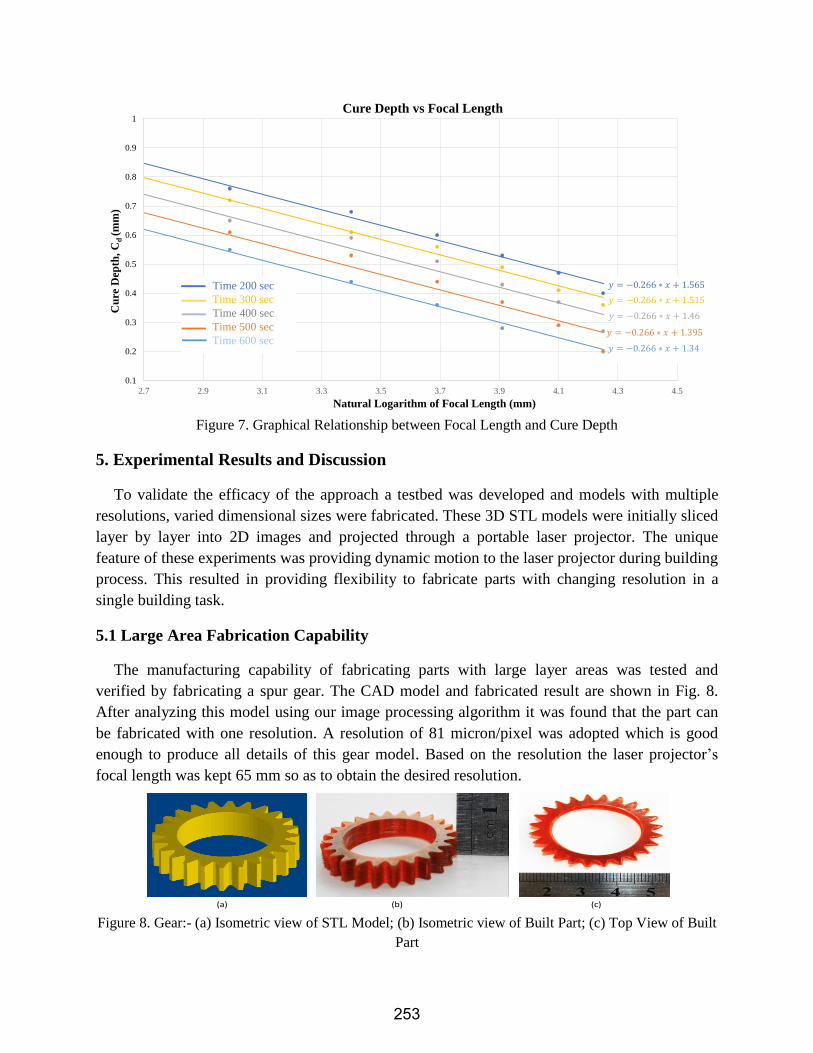
Figure 7. Graphical Relationship between Focal Length and Cure Depth
5. Experimental Results and Discussion
To validate the efficacy of the approach a testbed was developed and models with multiple
resolutions, varied dimensional sizes were fabricated. These 3D STL models were initially sliced
layer by layer into 2D images and projected through a portable laser projector. The unique
feature of these experiments was providing dynamic motion to the laser projector during building
process. This resulted in providing flexibility to fabricate parts with changing resolution in a
single building task.
5.1 Large Area Fabrication Capability
The manufacturing capability of fabricating parts with large layer areas was tested and
verified by fabricating a spur gear. The CAD model and fabricated result are shown in Fig. 8.
After analyzing this model using our image processing algorithm it was found that the part can
be fabricated with one resolution. A resolution of 81 micron/pixel was adopted which is good
enough to produce all details of this gear model. Based on the resolution the laser projector’s
focal length was kept 65 mm so as to obtain the desired resolution.
Figure 8. Gear:- (a) Isometric view of STL Model; (b) Isometric view of Built Part; (c) Top View of Built
Part
0.1
0.2
0.3
0.4
0.5
0.6
0.7
0.8
0.9
1
2.7 2.9 3.1 3.3 3.5 3.7 3.9 4.1 4.3 4.5
Cu
re D
epth
, C
d (
mm
)
Natural Logarithm of Focal Length (mm)
Cure Depth vs Focal Length
Time 200 sec
Time 300 sec
Time 400 sec
Time 500 sec
Time 600 sec
𝑦 = −0. 66 ∗ 𝑥 + 1.565
𝑦 = −0. 66 ∗ 𝑥 + 1.515
𝑦 = −0. 66 ∗ 𝑥 + 1.46
𝑦 = −0. 66 ∗ 𝑥 + 1.395
𝑦 = −0. 66 ∗ 𝑥 + 1.34
(a) (b) (c)
253
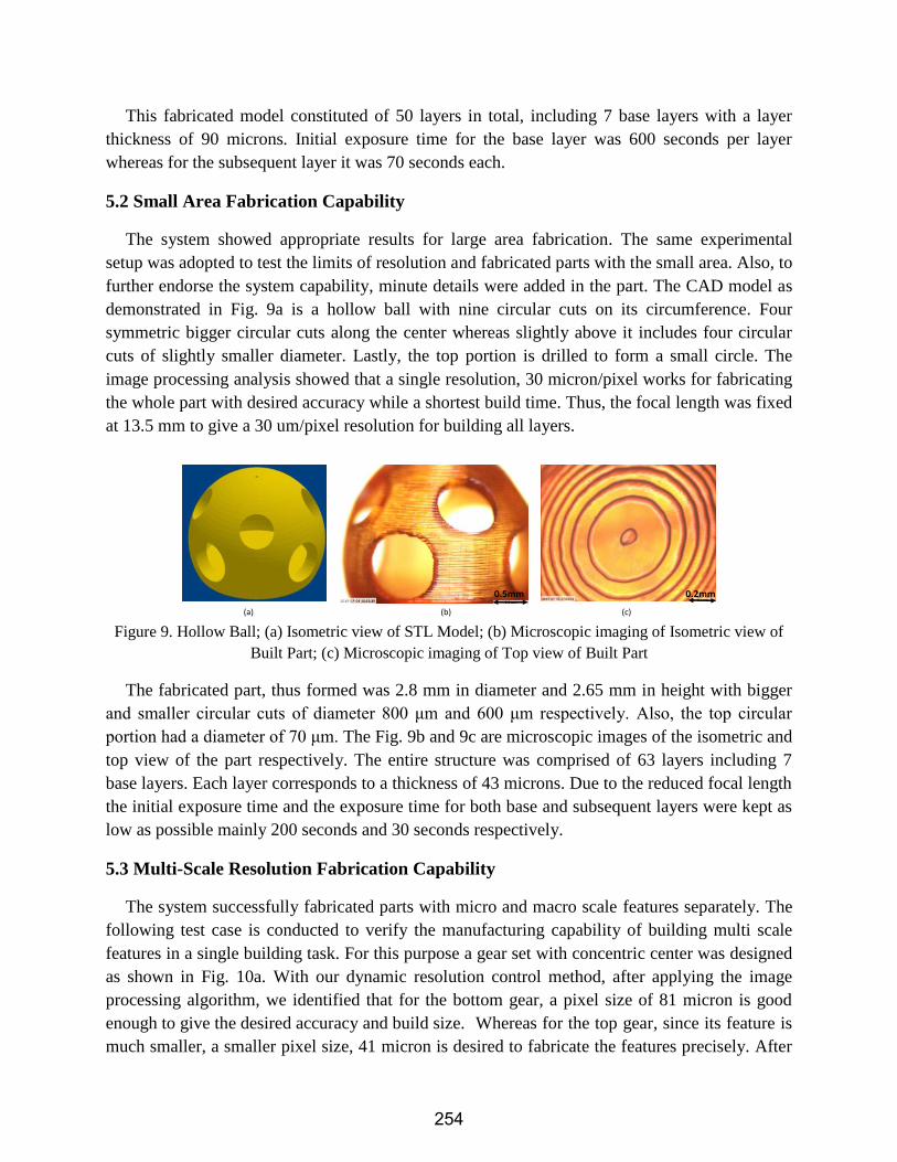
This fabricated model constituted of 50 layers in total, including 7 base layers with a layer
thickness of 90 microns. Initial exposure time for the base layer was 600 seconds per layer
whereas for the subsequent layer it was 70 seconds each.
5.2 Small Area Fabrication Capability
The system showed appropriate results for large area fabrication. The same experimental
setup was adopted to test the limits of resolution and fabricated parts with the small area. Also, to
further endorse the system capability, minute details were added in the part. The CAD model as
demonstrated in Fig. 9a is a hollow ball with nine circular cuts on its circumference. Four
symmetric bigger circular cuts along the center whereas slightly above it includes four circular
cuts of slightly smaller diameter. Lastly, the top portion is drilled to form a small circle. The
image processing analysis showed that a single resolution, 30 micron/pixel works for fabricating
the whole part with desired accuracy while a shortest build time. Thus, the focal length was fixed
at 13.5 mm to give a 30 um/pixel resolution for building all layers.
Figure 9. Hollow Ball; (a) Isometric view of STL Model; (b) Microscopic imaging of Isometric view of
Built Part; (c) Microscopic imaging of Top view of Built Part
The fabricated part, thus formed was 2.8 mm in diameter and 2.65 mm in height with bigger
and smaller circular cuts of diameter 800 μm and 600 μm respectively. Also, the top circular
portion had a diameter of 70 μm. The Fig. 9b and 9c are microscopic images of the isometric and
top view of the part respectively. The entire structure was comprised of 63 layers including 7
base layers. Each layer corresponds to a thickness of 43 microns. Due to the reduced focal length
the initial exposure time and the exposure time for both base and subsequent layers were kept as
low as possible mainly 200 seconds and 30 seconds respectively.
5.3 Multi-Scale Resolution Fabrication Capability
The system successfully fabricated parts with micro and macro scale features separately. The
following test case is conducted to verify the manufacturing capability of building multi scale
features in a single building task. For this purpose a gear set with concentric center was designed
as shown in Fig. 10a. With our dynamic resolution control method, after applying the image
processing algorithm, we identified that for the bottom gear, a pixel size of 81 micron is good
enough to give the desired accuracy and build size. Whereas for the top gear, since its feature is
much smaller, a smaller pixel size, 41 micron is desired to fabricate the features precisely. After
0.5mm
(a) (b) (c)
0.2mm
254
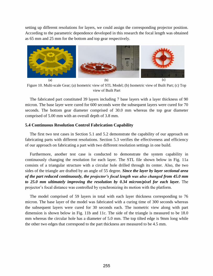
setting up different resolutions for layers, we could assign the corresponding projector position.
According to the parametric dependence developed in this research the focal length was obtained
as 65 mm and 25 mm for the bottom and top gear respectively.
Figure 10. Multi-scale Gear; (a) Isometric view of STL Model; (b) Isometric view of Built Part; (c) Top
view of Built Part
The fabricated part constituted 39 layers including 7 base layers with a layer thickness of 90
micron. The base layer were cured for 600 seconds were the subsequent layers were cured for 70
seconds. The bottom gear diameter comprised of 30.0 mm whereas the top gear diameter
comprised of 5.00 mm with an overall depth of 3.8 mm.
5.4 Continuous Resolution Control Fabrication Capability
The first two test cases in Section 5.1 and 5.2 demonstrate the capability of our approach on
fabricating parts with different resolutions. Section 5.3 verifies the effectiveness and efficiency
of our approach on fabricating a part with two different resolution settings in one build.
Furthermore, another test case is conducted to demonstrate the system capability in
continuously changing the resolution for each layer. The STL file shown below in Fig. 11a
consists of a triangular structure with a circular hole drilled through its center. Also, the two
sides of the triangle are drafted by an angle of 55 degree. Since the layer by layer sectional area
of the part reduced continuously, the projector’s focal length was also changed from 45.0 mm
to 25.0 mm ultimately improving the resolution by 0.34 micron/pixel for each layer. The
projector’s focal distance was controlled by synchronizing its motion with the platform.
The model comprised of 59 layers in total with each layer thickness corresponding to 76
micron. The base layer of the model was fabricated with a curing time of 300 seconds whereas
the subsequent layers were cured for 30 seconds each. The isometric view along with part
dimension is shown below in Fig. 11b and 11c. The side of the triangle is measured to be 18.0
mm whereas the circular hole has a diameter of 5.0 mm. The top tilted edge is 9mm long while
the other two edges that correspond to the part thickness are measured to be 4.5 mm.
(a) (b) (c)
255
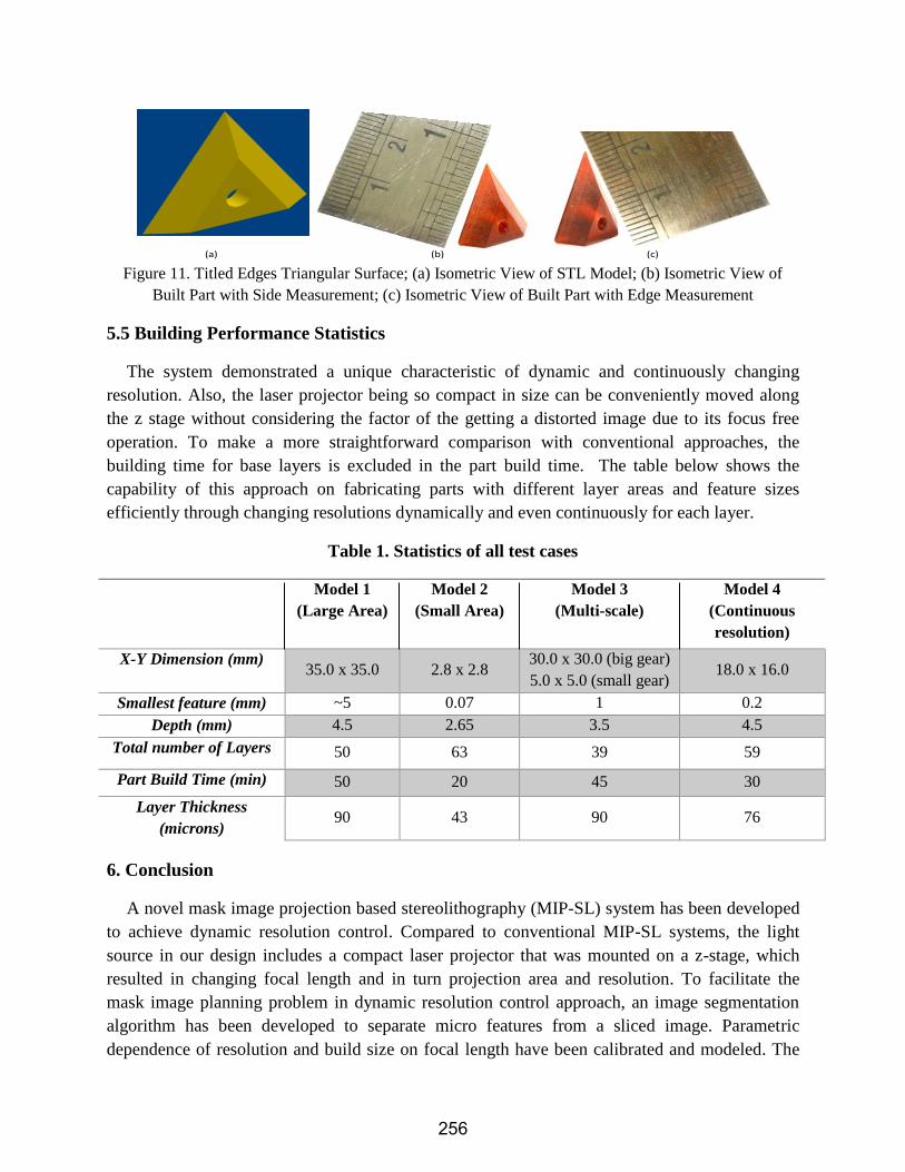
Figure 11. Titled Edges Triangular Surface; (a) Isometric View of STL Model; (b) Isometric View of
Built Part with Side Measurement; (c) Isometric View of Built Part with Edge Measurement
5.5 Building Performance Statistics
The system demonstrated a unique characteristic of dynamic and continuously changing
resolution. Also, the laser projector being so compact in size can be conveniently moved along
the z stage without considering the factor of the getting a distorted image due to its focus free
operation. To make a more straightforward comparison with conventional approaches, the
building time for base layers is excluded in the part build time. The table below shows the
capability of this approach on fabricating parts with different layer areas and feature sizes
efficiently through changing resolutions dynamically and even continuously for each layer.
Table 1. Statistics of all test cases
Model 1
(Large Area)
Model 2
(Small Area)
Model 3
(Multi-scale)
Model 4
(Continuous
resolution)
X-Y Dimension (mm) 35.0 x 35.0 2.8 x 2.8
30.0 x 30.0 (big gear)
5.0 x 5.0 (small gear) 18.0 x 16.0
Smallest feature (mm) ~5 0.07 1 0.2
Depth (mm) 4.5 2.65 3.5 4.5
Total number of Layers 50 63 39 59
Part Build Time (min) 50 20 45 30
Layer Thickness
(microns) 90 43 90 76
6. Conclusion
A novel mask image projection based stereolithography (MIP-SL) system has been developed
to achieve dynamic resolution control. Compared to conventional MIP-SL systems, the light
source in our design includes a compact laser projector that was mounted on a z-stage, which
resulted in changing focal length and in turn projection area and resolution. To facilitate the
mask image planning problem in dynamic resolution control approach, an image segmentation
algorithm has been developed to separate micro features from a sliced image. Parametric
dependence of resolution and build size on focal length have been calibrated and modeled. The
(a) (b) (c)
256

effectiveness and efficiency of the system has been verified with multiple test cases with various
surface areas, feature sizes and structures.
References
1. Ha, Y.M., et al., “Mass production of 3-D microstructures using projection
microstereolithography” Journal of mechanical science and technology, 2008. 22(3): p. 514-521.
2. Pan, Y., et al., “A Fast Mask Projection Stereolithography Process for Fabricating Digital Models
in Minutes” Journal of Manufacturing Science and Engineering-Transactions of the Asme, 2012.
134(5).
3. Pan, Y. and Y. Chen, “Smooth Surface Fabrication based on Controlled Meniscus and Cure
Depth in Micro-Stereolithography” 2015.
4. Pan, Y., et al., “Smooth surface fabrication in mask projection based stereolithography” Journal
of Manufacturing Processes, 2012. 14(4): p. 460-470.
5. Sun, C., et al., “Projection micro-stereolithography using digital micro-mirror dynamic mask”
Sensors and Actuators a-Physical, 2005. 121(1): p. 113-120.
6. Pan, Y., et al., “Multitool and Multi-Axis Computer Numerically Controlled Accumulation for
Fabricating Conformal Features on Curved Surfaces” Journal of Manufacturing Science and
Engineering-Transactions of the Asme, 2014. 136(3).
7. Turner, B.N., R. Strong, and S.A. Gold, “A review of melt extrusion additive manufacturing
processes: I. Process design and modeling” Rapid Prototyping Journal, 2014. 20(3): p. 192-204.
8. Zhao, X.J., et al., “An integrated CNC accumulation system for automatic building-around-
inserts” Journal of Manufacturing Processes, 2013. 15(4): p. 432-443.
9. Brett P. Conner, et al., “Making sense of 3D printing: Creating a map of additive manufacturing
products and services” Additive Manufacturing, Volume 1-4, October 2014, Page 64-76.
10. Klahn C., et al., "Laser additive manufacturing of gas permeable structures", Physics Procedia 41
(2013): 873-880.
11. Jane Chu, Sarah Engelbrecht, Gregory Graf, David W. Rosen, (2010) "A comparison of
synthesis methods for cellular structures with application to additive manufacturing" Rapid
Prototyping Journal, Vol. 16 Iss: 4, pp.275 – 283.
12. Huang, S.H., et al., “Additive manufacturing and its societal impact: a literature review” The
International Journal of Advanced Manufacturing Technology, 2013. 67(5-8): p. 1191-1203.
13. Choi, J.-W., et al., “Fabrication of 3D biocompatible/biodegradable micro-scaffolds using
dynamic mask projection microstereolithography” Journal of Materials Processing Technology,
2009. 209(15): p. 5494-5503.
257

14. Choi, J.W., et al., “Design of microstereolithography system based on dynamic image projection
for fabrication of three-dimensional microstructures” Journal of mechanical science and
technology, 2006. 20(12): p. 2094-2104.
15. Cheng, Y.-L. and M.-L. Lee, “Development of dynamic masking rapid prototyping system for
application in tissue engineering” Rapid Prototyping Journal, 2009. 15(1): p. 29-41.
16. Emami, Mohammad Mahdi, Farshad Barazandeh, and Farrokh Yaghmaie. "Scanning-projection
based stereolithography: Method and structure." Sensors and Actuators A: Physical 218 (2014):
116-124.
17. Microvision, Showmx Pico Projectors, http://www.microvision.com/wp-
content/uploads/2014/07/OPN_Article.pdf
18. Wang, C., and Chen, Y. "Layered depth-normal images: A sparse implicit representation of solid
models" arXiv preprint arXiv:1009.0794 (2010).
19. Envisiontec Perfactory Material Data Sheet, http://envisiontec.com/envisiontec/wp-
content/uploads/MK-MTS-R5R11-V01-FN-EN.pdf
20. Jacobs, Paul F., and David T. Reid. 1992. “Rapid prototyping & manufacturing: fundamentals of
stereolithography” Dearborn, MI: Society of Manufacturing Engineers in cooperation with the
Computer and Automated Systems Association of SME.
21. Gibson, Ian, David W. Rosen, and Brent Stucker, “Additive manufacturing technologies. New
York: Springer” 2010.
258