Embed Size (px)
Citation preview
Short communication
Dynamic finite element approach for analyzing stressand distortion in multilevel devices
A. Lakhsasi a,*, A. Skorek b
a Computer Engineering Department, Universit�ee du Qu�eebec, Hull, Qu�eebec, J8X 3X7, Canadab Industrial Electroheat Laboratory, University du Qu�eebec, Trois-Rivi�eeres, Qu�eebec, G9A-5H7, Canada
Received 12 February 2001
Abstract
Stress analysis is of crucial importance in the design of components and systems in the electronic industry. This
paper presents a dynamic finite element approach dynamic finite element approach for following the evolution of re-
sidual thermal stress during pulsed exposure of multilevel structures. A numerical example is given to demonstrate the
application of this approach. Its concern the transient thermal stress modeling of multilevel semiconductor devices
undergoing short pulses heating. We describe the elastic deformation of device due to thermal pulsed loading. The main
advantage of proposed approach is that it allows one to account for thermomechanical properties and conditions
changes during repetitive exposure heating, as well as the historical stresses and distortions introduced at each pulse. A
three-dimensional finite element model was constructed to simulate multilevel devices under short pulsed loading. The
temperature distributions obtained were used as input in order to compute thermal stress and mechanical deformations
of the multilevel structures. � 2002 Elsevier Science Ltd. All rights reserved.
Keywords: Finite element model; Thermal–mechanical behavior; Heat transfer; Thermal stress; Multilevel devices
1. Introduction
The electronic industry is faced with several chal-
lenges in the design, fabrication and packaging of elec-
tronic components, printed circuit boards (PCB) and
printed wiring boards (PWB). Multilevel structures are
common place in the electronic industry. Because these
structures are made of materials that have different
properties, specifically a different coefficient of thermal
expansion (CTE), thermal stresses, distortion and war-
page are a source of concern. Much of the effort is spent
in performing experiments to measure the stress and
temperature generated in the multilevel devices. This
work requires expensive amounts of time and money.
However, due to the complexity of these problems, no
analytical tool has been developed to solve them. The
multilevel structure of device increases the difficulty of
mechanical analysis since the behavior of structure is not
a simple average of single-layer behavior [1]. Dynamic
thermal behavior of multilevel structures during thermal
cycling has not been well characterized, and very few
researchers have reported a satisfactory way to analyze
effect of repetitive residual stress in multilevel device
problem [2]. In many case, it is important to understand
dynamic behavior of multilevel devices in order to en-
sure they fulfill safely their operation conditions.
The finite element method (FEM) has been widely
used by civil and mechanical engineers to build models
to estimate the stresses and distortion of structures
under a variety of loading conditions [3]. This technique
has also become popular in many electronic applications
and it has been applied to analyze a great number of
electronic structures ranging from power boards to
multilevel mask structures [4–7]. The application of the
FEM to determine the stresses that arise during pulsed
Solid-State Electronics 46 (2002) 925–932
* Tel.: +1-819-595-3900; fax: +1-819-773-1638.
E-mail address: [email protected]
(A. Lakhsasi).
0038-1101/02/$ - see front matter � 2002 Elsevier Science Ltd. All rights reserved.
PII: S0038-1101 (02 )00008-4
heating of multilevel structure is not always simple. The
reason is that in addition to subjecting the multilevel
structure to several thermal cycles, one has to consider
that the boundary conditions applied to the material
layers itself changes from one step of the process to
another. Moreover, if at least one material layer deforms
plastically, there is no easy way to keep track of the
stresses generated at one step of the analysis in order to
use them as initial conditions in the next step. In this
paper, we present dynamic thermal behavior of multi-
level mask devices as examples for presenting dynamic
finite element approach (DFEA) for analyzing stress and
distortion during thermal cycling.
X-ray lithography is anticipated to be an important
printing technology for fabrication of VLSI devices in
the vicinity of 0.25 lm and below. Mask heating during
X-ray lithography exposures is of concern since it may
cause pattern displacements (mask distortion and war-
page) and mechanical failure due to high stresses de-
veloped in the mask substrates and absorber films. Low
thermal distortion in the mask structure and patterns is
the key issue in achieving reproducibility for submicron
technology. Thermal distortions in the mask membrane
and absorber occur because the high radiation doses
needed to expose conventional resists cause temperature
rises in the mask, a key issue in achieving positional
accuracy in the mask in accounting for these distortions.
The thermal and mechanical modeling of X-ray masks
under short pulse irradiation has been studied by Sha-
reef et al. [5], Ballantyne et al. [2], Dym and Ballantyne
[8], Hyman et al. [9], Henrich et al. [10], and Lakhsasi
et al. [7]. In this paper, we present a dynamic approach
for following the evolution of residual thermal stress
during repetitive short pulses (1–100 ns) exposure of
multilevel structures. Thermal energy is thus deposited
very rapidly into the device structure, and since the heat
cannot be dissipated in such a short time, the potential
exists for damaging the structure. We have therefore
construct three dimensional (3D) finite element model to
simulate multilevel structures (example of X-rays mask)
under short pulse heating. The mechanics of multilevel
device failure are examined in terms of single pulse and
cumulative, or fatigue, effects.
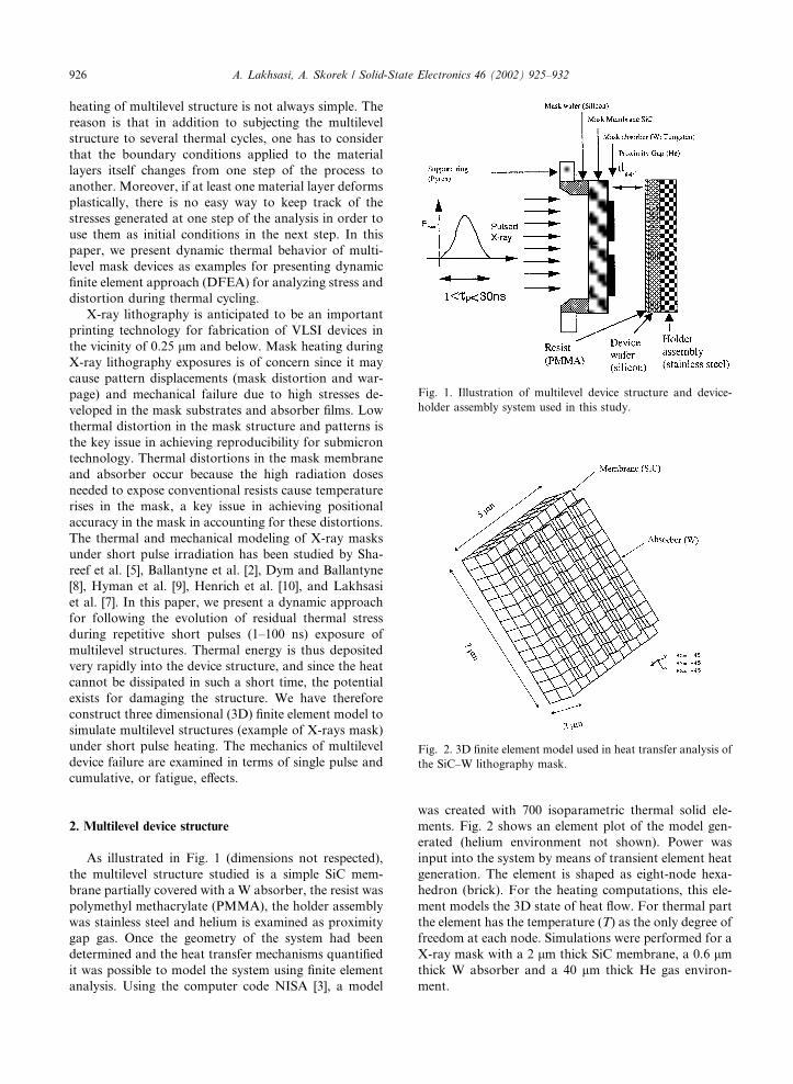
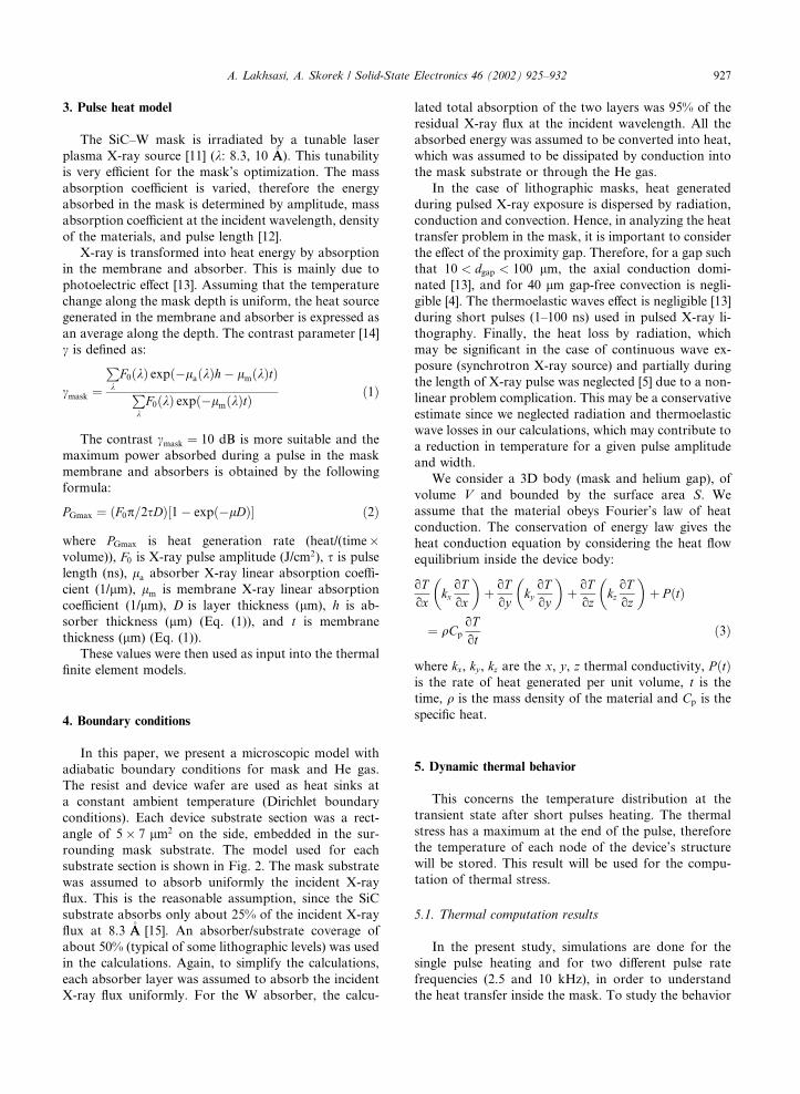
2. Multilevel device structure
As illustrated in Fig. 1 (dimensions not respected),
the multilevel structure studied is a simple SiC mem-
brane partially covered with a W absorber, the resist was
polymethyl methacrylate (PMMA), the holder assembly
was stainless steel and helium is examined as proximity
gap gas. Once the geometry of the system had been
determined and the heat transfer mechanisms quantified
it was possible to model the system using finite element
analysis. Using the computer code NISA [3], a model
was created with 700 isoparametric thermal solid ele-
ments. Fig. 2 shows an element plot of the model gen-
erated (helium environment not shown). Power was
input into the system by means of transient element heat
generation. The element is shaped as eight-node hexa-
hedron (brick). For the heating computations, this ele-
ment models the 3D state of heat flow. For thermal part
the element has the temperature (T) as the only degree of
freedom at each node. Simulations were performed for a
X-ray mask with a 2 lm thick SiC membrane, a 0.6 lmthick W absorber and a 40 lm thick He gas environ-
ment.
Fig. 1. Illustration of multilevel device structure and device-
holder assembly system used in this study.
Fig. 2. 3D finite element model used in heat transfer analysis of
the SiC–W lithography mask.
926 A. Lakhsasi, A. Skorek / Solid-State Electronics 46 (2002) 925–932
3. Pulse heat model
The SiC–W mask is irradiated by a tunable laser
plasma X-ray source [11] (k: 8.3, 10 �AA). This tunability
is very efficient for the mask’s optimization. The mass
absorption coefficient is varied, therefore the energy
absorbed in the mask is determined by amplitude, mass
absorption coefficient at the incident wavelength, density
of the materials, and pulse length [12].
X-ray is transformed into heat energy by absorption
in the membrane and absorber. This is mainly due to
photoelectric effect [13]. Assuming that the temperature
change along the mask depth is uniform, the heat source
generated in the membrane and absorber is expressed as
an average along the depth. The contrast parameter [14]
c is defined as:
cmask ¼
PkF0ðkÞ expð�laðkÞh� lmðkÞtÞP
kF0ðkÞ expð�lmðkÞtÞ
ð1Þ
The contrast cmask ¼ 10 dB is more suitable and the
maximum power absorbed during a pulse in the mask
membrane and absorbers is obtained by the following
formula:
PGmax ¼ ðF0p=2sDÞ½1� expð�lDÞ� ð2Þ
where PGmax is heat generation rate (heat/(time�volume)), F0 is X-ray pulse amplitude (J/cm2), s is pulse
length (ns), la absorber X-ray linear absorption coeffi-
cient (1/lm), lm is membrane X-ray linear absorption
coefficient (1/lm), D is layer thickness (lm), h is ab-
sorber thickness (lm) (Eq. (1)), and t is membrane
thickness (lm) (Eq. (1)).
These values were then used as input into the thermal
finite element models.
4. Boundary conditions
In this paper, we present a microscopic model with
adiabatic boundary conditions for mask and He gas.
The resist and device wafer are used as heat sinks at
a constant ambient temperature (Dirichlet boundary
conditions). Each device substrate section was a rect-
angle of 5� 7 lm2 on the side, embedded in the sur-
rounding mask substrate. The model used for each
substrate section is shown in Fig. 2. The mask substrate
was assumed to absorb uniformly the incident X-ray
flux. This is the reasonable assumption, since the SiC
substrate absorbs only about 25% of the incident X-ray
flux at 8.3 �AA [15]. An absorber/substrate coverage of
about 50% (typical of some lithographic levels) was used
in the calculations. Again, to simplify the calculations,
each absorber layer was assumed to absorb the incident
X-ray flux uniformly. For the W absorber, the calcu-
lated total absorption of the two layers was 95% of the
residual X-ray flux at the incident wavelength. All the
absorbed energy was assumed to be converted into heat,
which was assumed to be dissipated by conduction into
the mask substrate or through the He gas.
In the case of lithographic masks, heat generated
during pulsed X-ray exposure is dispersed by radiation,
conduction and convection. Hence, in analyzing the heat
transfer problem in the mask, it is important to consider
the effect of the proximity gap. Therefore, for a gap such
that 10 < dgap < 100 lm, the axial conduction domi-
nated [13], and for 40 lm gap-free convection is negli-
gible [4]. The thermoelastic waves effect is negligible [13]
during short pulses (1–100 ns) used in pulsed X-ray li-
thography. Finally, the heat loss by radiation, which
may be significant in the case of continuous wave ex-
posure (synchrotron X-ray source) and partially during
the length of X-ray pulse was neglected [5] due to a non-
linear problem complication. This may be a conservative
estimate since we neglected radiation and thermoelastic
wave losses in our calculations, which may contribute to
a reduction in temperature for a given pulse amplitude
and width.
We consider a 3D body (mask and helium gap), of
volume V and bounded by the surface area S. We
assume that the material obeys Fourier’s law of heat
conduction. The conservation of energy law gives the
heat conduction equation by considering the heat flow
equilibrium inside the device body:
oTox
kxoTox
� �þ oT
oykyoToy
� �þ oT
ozkzoToz
� �þ P ðtÞ
¼ qCp
oTot
ð3Þ
where kx, ky , kz are the x, y, z thermal conductivity, P ðtÞis the rate of heat generated per unit volume, t is the
time, q is the mass density of the material and Cp is the
specific heat.
5. Dynamic thermal behavior
This concerns the temperature distribution at the
transient state after short pulses heating. The thermal
stress has a maximum at the end of the pulse, therefore
the temperature of each node of the device’s structure
will be stored. This result will be used for the compu-
tation of thermal stress.
5.1. Thermal computation results
In the present study, simulations are done for the
single pulse heating and for two different pulse rate
frequencies (2.5 and 10 kHz), in order to understand
the heat transfer inside the mask. To study the behavior
A. Lakhsasi, A. Skorek / Solid-State Electronics 46 (2002) 925–932 927
of the mask under repetitive pulses, computations are
performed for few pulses (seven). The evolution of the
temperature is recorded in three different levels of the
mask: in the middle of the membrane (node 250), at
the SiC–W interface (node 580) and at the W–He in-
terface (node 910). Fig. 3 shows the evolution of the
temperature at the three different levels of the mask
for the corresponding numerical values: kSiC ¼ 0:41 W/
cm �C, s ¼ 2 ns, k ¼ 8:3 �AA and F ¼ 10 mJ/cm2. As
shown in Fig. 3, a non-uniform temperature profile ex-
ists through the device thickness at the end of the pulse.
This leads to generation of considerable thermal stress
across the absorber/substrate interface, this is examined
in detail in Ref. [16]. After the end of pulse heating, there
is subsequent relaxation on temperature gradients
through the structure leading to an essentially uniform
temperature variation (Fig. 3). The cooling of the device
is essentially controlled by conduction through to the
resist and its substrate (Fig. 1). Table 1 gives the ther-
momechanical parameters for different materials used in
the computation [17].
Under these conditions, the maximum thermal vari-
ation DT is 26.9 �C. It is observed that the maximum
temperature occurs at the completion of the X-ray pulse
(Fig. 3). The temperature then decays exponentially with
a time constant determined by the conduction of heat
from the SiC–W interface into the SiC membrane and
into the W absorbers. After this, the temperature re-
mains fairly constant until heat conduction through the
He gas into the heat sink begins. It is observed from the
Fig. 3 that, the mask reaches the initial temperature after
about 5 ms. This indicates that it is possible to operate
with 200 Hz repetition rate and 10 mJ/cm2 pulses with-
out causing any appreciable average heating in the mask
under the assumed conditions. The simulation shows
that the mask thermal stability (thermal equilibration) is
reached after 30 ns.
At this stage of the simulation, it is interesting to see
the effect of the residual thermal energy on the mask’s
temperature variation. If a second pulse is started at 0.4
ms from the first (f ¼ 2:5 kHz), Fig. 4 gives the evolu-
tion of the temperature at the SiC–W interface (seven
pulses only). A residual thermal energy leads to an in-
crease of the thermal peak and stabilization temperature
variation (17–25 �C). As discussed later, this augmen-
tation is accumulated from one pulse to the other im-
plying gradual deterioration of the mask.
The SiC–W device is subject to intense repetitive
short pulsed X-ray. Thermal energy is thus deposited
very rapidly (few nanoseconds) into the X-ray mask
structure, the heat cannot be dissipated in such a short
time, so the potential exists for damaging the mask.
Therefore, the large temperature gradient across the
Fig. 3. Temperature behavior at the three different levels of the
mask for kSiC ¼ 0:41 W/cm �C, s ¼ 2 ns, k ¼ 8:3 �AA and F ¼ 10
mJ/cm2.
Fig. 4. Effect of thermal energy accumulation on evolution of
temperature in the SiC–W interface for 0.4 and 0.1 ms period
(f ¼ 2:5 and 10 kHz).
Table 1
Thermomechanical parameters
Materials k a m l at 8 �AA l at 10 �AA E D Cp d
SiC 0.41/3.50 2.3 0.27 0.2 0.3 1.75 2 0.19 3.2
1W 1.78 4.5 0.4 3 5 2.4 0.6 0.13 19.3
He 1.4E–3 – – 0.025 0.056 – 40 5.19 0.18E�3
m: poisson’s ratio, k: thermal conductivity (W/cm �C), a: thermal expansion (10�6/�C), E: Young’s modulus (�102 GPa), d: density (g/
cm3), C: specific heat (J/g �C), D: layer thickness (lm).
928 A. Lakhsasi, A. Skorek / Solid-State Electronics 46 (2002) 925–932
interface region can be expected to contribute to the
generation of critical thermal stress.
6. Dynamic thermal stress modeling
The electronics industry still follows a so-called
‘‘design-build test’’ scheme, i.e., measuring the bow and
twist on the prototype devices for predicting stress and
distortion. This setup has two drawbacks. First, building
prototypes and redesigns (if necessary) is a time con-
suming and expensive process; it will further prolong
product development cycle time. As such, electronics
companies may incur loss of market share. Second, test
alone does not offer sufficient insight and understanding
about the behaviors of device structures and materials.
Furthermore, device engineering needs a logical, ratio-
nal, scientific basis underlying the physical nature of the
phenomenon. It will be extremely helpful if designers are
able to utilize computer-based software tools to analyt-
ically simulate physical behaviors of multilevel devices
in the early design phases of the design process.
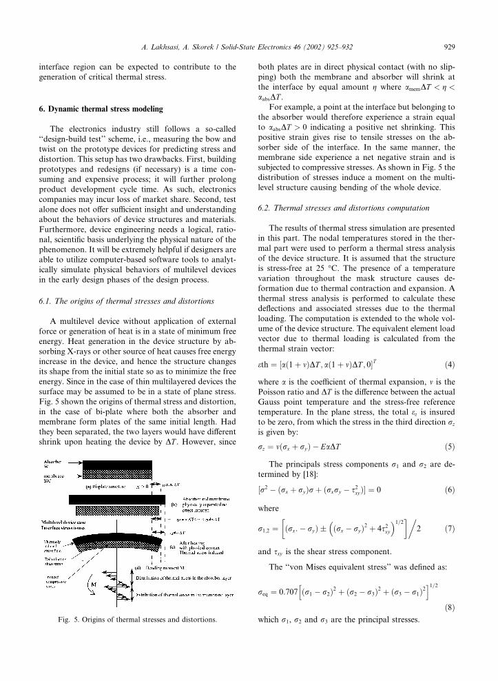
6.1. The origins of thermal stresses and distortions
A multilevel device without application of external
force or generation of heat is in a state of minimum free
energy. Heat generation in the device structure by ab-
sorbing X-rays or other source of heat causes free energy
increase in the device, and hence the structure changes
its shape from the initial state so as to minimize the free
energy. Since in the case of thin multilayered devices the
surface may be assumed to be in a state of plane stress.
Fig. 5 shown the origins of thermal stress and distortion,
in the case of bi-plate where both the absorber and
membrane form plates of the same initial length. Had
they been separated, the two layers would have different
shrink upon heating the device by DT . However, since
both plates are in direct physical contact (with no slip-
ping) both the membrane and absorber will shrink at
the interface by equal amount g where amemDT < g <aabsDT .
For example, a point at the interface but belonging to
the absorber would therefore experience a strain equal
to aabsDT > 0 indicating a positive net shrinking. This
positive strain gives rise to tensile stresses on the ab-
sorber side of the interface. In the same manner, the
membrane side experience a net negative strain and is
subjected to compressive stresses. As shown in Fig. 5 the
distribution of stresses induce a moment on the multi-
level structure causing bending of the whole device.
6.2. Thermal stresses and distortions computation
The results of thermal stress simulation are presented
in this part. The nodal temperatures stored in the ther-
mal part were used to perform a thermal stress analysis
of the device structure. It is assumed that the structure
is stress-free at 25 �C. The presence of a temperature
variation throughout the mask structure causes de-
formation due to thermal contraction and expansion. A
thermal stress analysis is performed to calculate these
deflections and associated stresses due to the thermal
loading. The computation is extended to the whole vol-
ume of the device structure. The equivalent element load
vector due to thermal loading is calculated from the
thermal strain vector:
eth ¼ að1½ þ mÞDT ; að1þ mÞDT ; 0�T ð4Þ
where a is the coefficient of thermal expansion, m is the
Poisson ratio and DT is the difference between the actual
Gauss point temperature and the stress-free reference
temperature. In the plane stress, the total ez is insured
to be zero, from which the stress in the third direction rz
is given by:
rz ¼ mðrx þ ryÞ � EaDT ð5Þ
The principals stress components r1 and r2 are de-
termined by [18]:
½r2 � ðrx þ ryÞr þ ðrxry � s2xyÞ� ¼ 0 ð6Þ
where
r1;2 ¼ ðrx:
�� ryÞ ðrx
�� ryÞ2 þ 4s2xy
�1=2�
2
�ð7Þ
and sxy is the shear stress component.
The ‘‘von Mises equivalent stress’’ was defined as:
req ¼ 0:707 ðr1
h� r2Þ2 þ ðr2 � r3Þ2 þ ðr3 � r1Þ2
i1=2ð8Þ
which r1, r2 and r3 are the principal stresses.Fig. 5. Origins of thermal stresses and distortions.
A. Lakhsasi, A. Skorek / Solid-State Electronics 46 (2002) 925–932 929
The ‘‘second principal stress’’ r2 is acting in the plane
of the multilevel structure and r1 is the ‘‘first principal
stress’’. In the following, the ‘‘second principal stress’’ is
presented. It is assumed that the mask’s structure is free
of intrinsic stress (at 25 �C). Finally, the ‘‘IPD’’ was
defined as: in-plane distortions of structure (XZ plane
resultant displacement), and ‘‘OPD’’ was defined as:
out-of-plane distortions (warpage) of structure (Y dis-
placement).
6.3. Thermal stresses and distortions results
6.3.1. Limit of stress and failure criteria
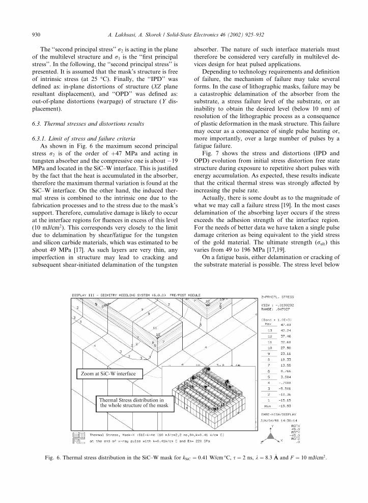
As shown in Fig. 6 the maximum second principal
stress r2 is of the order of þ47 MPa and acting in
tungsten absorber and the compressive one is about �19
MPa and located in the SiC–W interface. This is justified
by the fact that the heat is accumulated in the absorber,
therefore the maximum thermal variation is found at the
SiC–W interface. On the other hand, the induced ther-
mal stress is combined to the intrinsic one due to the
fabrication processes and to the stress due to the mask’s
support. Therefore, cumulative damage is likely to occur
at the interface regions for fluences in excess of this level
(10 mJ/cm2). This corresponds very closely to the limit
due to delamination by shear/fatigue for the tungsten
and silicon carbide materials, which was estimated to be
about 49 MPa [17]. As such layers are very thin, any
imperfection in structure may lead to cracking and
subsequent shear-initiated delamination of the tungsten
absorber. The nature of such interface materials must
therefore be considered very carefully in multilevel de-
vices design for heat pulsed applications.
Depending to technology requirements and definition
of failure, the mechanism of failure may take several
forms. In the case of lithographic masks, failure may be
a catastrophic delamination of the absorber from the
substrate, a stress failure level of the substrate, or an
inability to obtain the desired level (below 10 nm) of
resolution of the lithographic process as a consequence
of plastic deformation in the mask structure. This failure
may occur as a consequence of single pulse heating or,
more importantly, over a large number of pulses by a
fatigue failure.
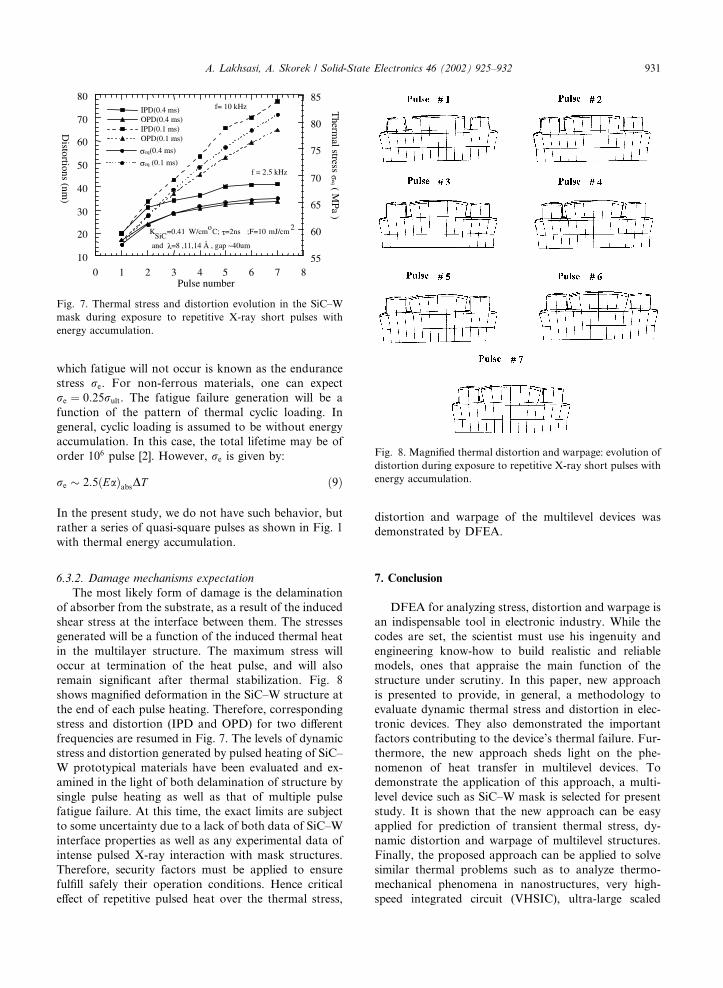
Fig. 7 shows the stress and distortions (IPD and
OPD) evolution from initial stress distortion free state
structure during exposure to repetitive short pulses with
energy accumulation. As expected, these results indicate
that the critical thermal stress was strongly affected by
increasing the pulse rate.
Actually, there is some doubt as to the magnitude of
what we may call a failure stress [19]. In the most cases
delamination of the absorbing layer occurs if the stress
exceeds the adhesion strength of the interface region.
For the needs of better data we have taken a single pulse
damage criterion as being equivalent to the yield stress
of the gold material. The ultimate strength (rult) this
varies from 49 to 196 MPa [17,19].
On a fatigue basis, either delamination or cracking of
the substrate material is possible. The stress level below
Fig. 6. Thermal stress distribution in the SiC–W mask for kSiC ¼ 0:41 W/cm �C, s ¼ 2 ns, k ¼ 8:3 �AA and F ¼ 10 mJ/cm2.
930 A. Lakhsasi, A. Skorek / Solid-State Electronics 46 (2002) 925–932
which fatigue will not occur is known as the endurance
stress re. For non-ferrous materials, one can expect
re ¼ 0:25rult. The fatigue failure generation will be a
function of the pattern of thermal cyclic loading. In
general, cyclic loading is assumed to be without energy
accumulation. In this case, the total lifetime may be of
order 106 pulse [2]. However, re is given by:
re 2:5ðEaÞabsDT ð9Þ
In the present study, we do not have such behavior, but
rather a series of quasi-square pulses as shown in Fig. 1
with thermal energy accumulation.
6.3.2. Damage mechanisms expectation
The most likely form of damage is the delamination
of absorber from the substrate, as a result of the induced
shear stress at the interface between them. The stresses
generated will be a function of the induced thermal heat
in the multilayer structure. The maximum stress will
occur at termination of the heat pulse, and will also
remain significant after thermal stabilization. Fig. 8
shows magnified deformation in the SiC–W structure at
the end of each pulse heating. Therefore, corresponding
stress and distortion (IPD and OPD) for two different
frequencies are resumed in Fig. 7. The levels of dynamic
stress and distortion generated by pulsed heating of SiC–
W prototypical materials have been evaluated and ex-
amined in the light of both delamination of structure by
single pulse heating as well as that of multiple pulse
fatigue failure. At this time, the exact limits are subject
to some uncertainty due to a lack of both data of SiC–W
interface properties as well as any experimental data of
intense pulsed X-ray interaction with mask structures.
Therefore, security factors must be applied to ensure
fulfill safely their operation conditions. Hence critical
effect of repetitive pulsed heat over the thermal stress,
distortion and warpage of the multilevel devices was
demonstrated by DFEA.
7. Conclusion
DFEA for analyzing stress, distortion and warpage is
an indispensable tool in electronic industry. While the
codes are set, the scientist must use his ingenuity and
engineering know-how to build realistic and reliable
models, ones that appraise the main function of the
structure under scrutiny. In this paper, new approach
is presented to provide, in general, a methodology to
evaluate dynamic thermal stress and distortion in elec-
tronic devices. They also demonstrated the important
factors contributing to the device’s thermal failure. Fur-
thermore, the new approach sheds light on the phe-
nomenon of heat transfer in multilevel devices. To
demonstrate the application of this approach, a multi-
level device such as SiC–W mask is selected for present
study. It is shown that the new approach can be easy
applied for prediction of transient thermal stress, dy-
namic distortion and warpage of multilevel structures.
Finally, the proposed approach can be applied to solve
similar thermal problems such as to analyze thermo-
mechanical phenomena in nanostructures, very high-
speed integrated circuit (VHSIC), ultra-large scaled
Fig. 7. Thermal stress and distortion evolution in the SiC–W
mask during exposure to repetitive X-ray short pulses with
energy accumulation.
Fig. 8. Magnified thermal distortion and warpage: evolution of
distortion during exposure to repetitive X-ray short pulses with
energy accumulation.
A. Lakhsasi, A. Skorek / Solid-State Electronics 46 (2002) 925–932 931
integrated circuit (ULSI), surface mount technology
(SMT), plastic DIP mounted on PC board etc. or simply
to determine the junction temperatures and stresses of
multiple power components.
References
[1] Cifuentes AO, Shareef IA. Modeling of multilevel struc-
tures: a general method for analyzing stress evolution
during processing. IEEE Trans Semicond Manufact
1992;5(2):128–37.
[2] Ballantyne A, Hyman H, Dym C, Southworth R. Response
of lithographic mask structures to intense repetitively
pulsed X-rays: thermal stress analysis. J Appl Phys
1985;58(12):4717.
[3] Engineering Mechanics Research Corporation (EMRC).
Publication manual. Michigan, Troy, EMRC NISA II,
1987.
[4] Chiba A, Okada K. Dynamic in-plane thermal distortion
analysis of an X-ray mask membrane for synchrotron
radiation lithography. J Vac Sci Technol B 1991;9:3275–9.
[5] Shareef I, Maldonado J, Katcoff D. Thermal and mechan-
ical model of X-ray lithography masks under short pulse
irradiation. J Vac Sci Technol B 1989;7(6):1575.
[6] Yeh CP, Ume C, Fulton RE, Wyatt KW, Stafford JW.
Correlation of analytical and experimental approaches to
determine thermally induced PWB warpage. IEEE Trans
Comp Hybrids Manufact Technol 1993;16(8):986–95.
[7] Lakhsasi A, P�eepin H, Skorek A. Transient thermal
stability of the X-ray mask SiC–W under short pulse
irradiation. J Simul Practice Theory (SIMPRA97) 1997;
5(4):315–31.
[8] Dym CL, Ballantyne A. Response of lithographic mask
structures to intense repetitively pulsed X-rays: dynamic
response analysis. J Appl Phys 1985;58(12):4726.
[9] Hyman H, Ballantyne A, Friedmann HW, Reilly DA,
Southworth RC, Dym CL. Intense-pulsed plasma X-ray
sources for lithography: mask damage effects. J Vac Sci
Technol 1982;21(4):1012.
[10] Heinrich K, Betz H, Heuberger A. Heating and tempera-
ture-induced distortions of silicon X-ray masks. J Vac Sci
Technol B 1983;1(4):1352.
[11] P�eepin H, Alaterre P, Chaker M. X-ray sources for
microlithography created by laser radiation at k ¼ 0:26
lm. J Vac Sci Technol B 1987;5(1):27.
[12] Jean A, Chaker M, Diawara Y, Leung PK, Gat E, Mercier
PP, et al. Characterization of a-SiC:H films produced
in standard plasma enhanced chemical vapor deposition
system for X-ray mask application. J Appl Phys 1992;
72(7):3110.
[13] Chiba A, Okada K. Dynamic thermal distortion in an X-
ray mask membrane during pulsed X-ray exposure. Jpn J
Appl Phys 1990;29(11):2610–5.
[14] Henke BL et al. Atom Data Nucl Data Tables 1982;
27(1):373p.
[15] Maldonado JR. X-ray lithography where it is now and
where it is going. In: Proceedings Symposium on Electri-
cally Active Defects in Semiconductor––Insulator Systems,
Microelectronics Center of North Carolina, September.
1989.
[16] Lakhsasi A, Skorek A. Thermal stress computation in the
X-ray masks using finite element method. In: Proceedings
of the ISCA, 11th International Conference on Computer
Applications in Industry and Engineering (CAINE-98),
Las Vegas, Nevada, USA, November 11–13, 1998. p.
272–7.
[17] ASM engineered materials reference book, ASM Inter-
national, Metals Park, OH, 1988.
[18] Timoshenko S. Theory of elasticity. New York: McGraw-
Hill; 1934.
[19] Maissel LI, Glang R. Handbook of thin film technology.
New York: McGraw-Hill; 1970.
932 A. Lakhsasi, A. Skorek / Solid-State Electronics 46 (2002) 925–932