Embed Size (px)
Citation preview
Journal of Ceramic Processing Research. Vol. 13, Special. 1, pp. s1~s5 (2012)
s1
J O U R N A L O F
CeramicProcessing Research
Dye-sensitized solar cells fabricated with size-selected titanium dioxide nanowires
via an electrospinning method
Suk In Noh and Hyo-Jin Ahn*
Department of Materials Science & Engineering, Seoul National University of Science and Technology, Seoul, 139-743, Korea
Two types of size-selected titanium dioxide (TiO2) nanowires (NWs) have been successfully synthesized via an electrospinningmethod and their structural and photovoltaic features investigated for use as a photoelectrode in dye-sensitized solar cells(DSSCs). Scanning electron microscopy (SEM), transmission electron microscopy (TEM), X-ray diffraction (XRD), and X-rayphotoelectron spectroscopy (XPS) results show that two types of size-selected TiO2 NWs, which are made of anatase and rutilephases, have average diameters of ~100 nm and ~30 nm. Photocurrent-voltage curves show that the TiO2 NW photoelectrodesfabricated with a ~30 nm diameter exhibit a superior short-circuit current density of 10.86 mA/cm2 and a cell efficiency of3.93%, for an area of 0.196 cm2 compared to those fabricated with a ~100 nm diameter, which is attributed to the increasedspecific surface area that allows for a higher rate of dye adsorption.
Key words: Electrospinning, TiO2, Nanowires, Photovoltaic studies, Dye-sensitized solar cells.
Introduction
Dye-sensitized solar cells (DSSCs) are composed of a
nano-sized TiO2 photoelectrode sensitized by dye
molecules, an electrolyte, a counter electrode, and a
transparent conducting substrate. They have been of
great interest because of the advantages such as low-cost
fabrication, a less toxic manufacturing environment, and
flexibility of devices compared with the conventional
solid state junction devices [1, 2]. Several factors may
affect the performance in DSSCs, such as the size and
structure of the electrodes, the size of the electrode’s
holes, the chemical properties of the dye, the electrical
properties of the electrolyte, electrical and structural
properties of the counter electrode, the ability to absorb
light, the intensity of the light, and et al. [3]. Of these
factors, the size and the structure of the electrodes are
important for improving photovoltaic efficiency in
DSSCs. Indeed, TiO2 nanoparticles have been most
widely used as anode materials for DSSCs [4, 5], and
now, TiO2 is currently one of most interesting materials
used as a photoanode in DSSCs because of the low-
cost, easy controllability of its morphology, and its
chemical stability [6].
One-dimensional nanostructured photoelectrodes in
DSSCs have recently been studied extensively in
regards to the morphology of materials because of their
unique electrical, electrochemical, and optical properties
[6-8]. For example, Mukherjee et al. reported that electro-
spun TiO2 nanofibers with a diameter of ~150 nm in
DSSCs exhibit effective electron diffusion coefficients
due to their polycrystalline nature and random web
structure [9]. Onozuka et al. reported DSSCs comprising
of TiO2 nanofibers with high surface areas via
electrospinning. TiO2 nanofibers fabricated with a
diameter of ~250 nm showed a cell efficiency of 4.4%
in an adjusted membrane thickness of 3.9 µm [10]. More
recently, Oh et al. studied the fabrication of TiO2 branched
nanowires using a seeding method for DSSCs and
obtained an improved short-circuit current density and cell
efficiency of 12.18 mA/cm2 and 4.3% compared to the
TiO2 nanowires [11]. In particular, in the case of one-
dimensional nanostructures, the efficiency of the DSSCs
was mainly limited by low dye adsorption and low surface
area of one-dimensional NWs [12]. Therefore, a study
between the photovoltaic properties and the size/
structure of electrodes in one-dimensional nanostructures
for use as a photoelectrode in DSSCs still remains.
In this work, two types of size-selected TiO2 NWs
were synthesized via electrospinning and a relationship
between their size/structure and photovoltaic properties
was demonstrated. Also, an electrospinning method was
used to fabricate TiO2 NWs for use as a photoanode in
DSSCs because of the several advantages, such as a
simple process, easy controllability of NW dimensions,
and good repeatability [13-16].
Experimental Procedures
A titanium precursor solution consisting of Ti (OiPr)4(Aldrich) and acetic acid (Aldrich) was mixed with
3 ml of anhydrous ethanol (Aldrich) and constantly
stirred for approximately ten minutes. Then it was
added into 7.5 ml of ethanol that contained 0.45 g of
*Corresponding author: Tel : +82-2-970-6622Fax: +82-2-973-6657E-mail: [email protected]

s2 Suk In Noh and Hyo-Jin Ahn
Polyvinylpyrrolidone (PVP, Mw = 1,300,000 g/mol). The
mixed solution for electrospinning was left to rest for
thirty minutes before it was loaded into the syringe pump.
Among the several parameters in an electrospinning
technique, an applied voltage and a needle gauge are
important in controlling the size of the NWs. For TiO2
NWs having a diameter of ~100 nm, a 23-gauge
stainless steel needle was equipped on a 12 ml plastic
syringe. The feeding rate was controlled to 0.04 ml/h
under an applied voltage of ~8 kV. For TiO2 NWs
having a diameter of ~30 nm, a 32-gauge needle was
used, and the feeding rate was controlled to 0.10 ml/h
under an applied voltage of ~20 kV. The distance of the
needle and collector was fixed to ~8 cm in both cases.
Aluminum foil was used as a collector as well.
Calcination at 500 οC for five hours was carried out to
selectively eliminate polymer. The morphologies of the
samples were measured by field emission scanning
electron microscopy (FE-SEM, Hitachi S-4100) and
transmission electron microscopy (TEM, TECNAI-
F20). The crystallinity and chemical bonding states of
the samples were carried out by X-ray diffraction
(XRD, Rigaku Rint 2500 with a Cu Kα radiation) and
X-ray photoemission spectroscopy (XPS, ESCALAB
250 with an Al Kα X-ray source). For the light
absorption properties of the samples, a UV-Visible
spectrophotometer (UV-Vis), the Jasco V650, was used
and it measured in the range of 200 nm to 900 nm.
DSSCs were fabricated by a conventional method to
investigate photovoltaic efficiency of the size-selected
TiO2 NWs. Ground paste, the weight of which
consisted of 16.2% of TiO2, 11.9% of hydroxypropyl
cellulose (HPC, Mw ~80,000, Aldrich), 4.4% of acetyl
acetone, and 67.5% of DI (De-ionized) water, was
applied on an F-doped SnO2 (FTO, 15 Ω/cm2) coated
glass using a squeeze printing in the size of 0.196 cm2,
and afterwards annealed at 500 οC for one hour and
then immersed into the 0.5 mM/L of Ru-535-bisTBA,
known as N719, (Solaronix) solution as well. A
platinum covered counter electrode and an as-prepared
working electrode were overlapped and an electrolyte
was filled between the counter and working electrode.
Photocurrent-voltage curves were measured under the
irradiation of a 150 watt xenon lamp (LAB 50) together
with the level of standard irradiance (AM 1.5 simulated
sunlight) with an intensity of 100 mW/cm2.
Results and Discussion
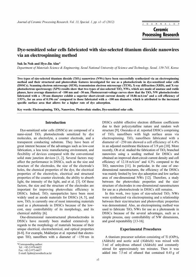
Figure 1 shows SEM images of size-selected TiO2
NWs having two different diameters after calcination at
500 οC. All the samples represent the morphology of
uniform NWs. Two types of the size-selected TiO2
NWs have average diameters of ~100 nm and ~30 nm,
respectively. Figure 2 presents TEM images of the
NWs obtained from an electrospinning method. The
TiO2 NWs of Figure 2(a) and Figure 2(b) are shown to
be ~100 nm and ~30 nm in diameter, respectively. TiO2
NWs with ~100 nm diameter and with ~30 nm diameter
seem to be composed of nanoparticles (or nano-grains)
with 5~10 nm size and 10~20 nm size as shown in the
insets of Figure 2. Two types of TiO2 NWs having
~100 nm diameter and ~30 nm diameter reveal diffuse
ring-like patterns containing spots around (000) plane,
indicating that their polycrystalline properties are well
in agreement with the XRD results.
To further investigate the structure and crystallinity
of all the NWs, XRD examinations were carried out as
shown in Figure 3. Crystal structures of electro-spun
TiO2 NWs consist of anatase and rutile phases. That is,
the XRD peaks of two samples are in good agreement
with those of anatase TiO2 structure (25.3°, 37.8°, 48.0°,
53.8°, 62.7°, and 68.8°, space group I41/amd (141))
[JCPDS card No. 841286] and rutile TiO2 structure
(27.4°, 36.0°, 41.2°, 54.3°, and 56.6°, space group p42/
Fig. 1. SEM images of TiO2 NW photoelectrodes with (a)~100 nm and (c) ~30 nm in diameter after calcination at 500 ο
C.Figure (b) and (d) present enlarged SEM images of Figure (a) and(c), respectively.
Fig. 2. The TEM images of the TiO2 NW photoelectrodes with (a)~100 nm and (b) ~30 nm in diameter fabricated via electrospinning.The insets exhibit SAED patterns and enlarged TEM images of thesamples.

Dye-sensitized solar cells fabricated with size-selected titanium dioxide nanowires via an electrospinning method... s3
mnm (136)) [JCPDS card No. 870920]. Furthermore,
the peak intensity of the (101) plane at 25.2° on the
anatase phases is higher than that of the (110) plane at
27.4° on the rutile phases as shown in Figure 3. This
implies that all the samples of the electro-spun TiO2
NWs are mainly formed along the (101) of the anatase
phases rather than the (110) of the rutile phases.
Figure 4 represents the XPS spectra obtained from
two samples to examine the chemical bonding states of
titanium and oxygen atoms. Figure 4(a) and 4(b)
exhibit the XPS core-level spectra for the Ti 2p3/2 and
Ti 2p1/2 photoelectrons at ~458.4 eV and ~464.0 eV for
two types of TiO2 NWs having a ~100 nm diameter
and a ~30 nm diameter, respectively. This implies that
the elemental titanium in the TiO2 is existing not as a
Ti(II) species, but a Ti(IV) species. Figure 4(c) and
4(d) exhibit the XPS core-level spectra for the oxygen
1s photoelectrons at ~529.6 eV for two samples with a
~100 nm diameter and a ~30 nm diameter, indicating
that the elemental oxygen species in the TiO2 is
existing as an O(II) species, which arises from the bulk
oxygen atoms [17]. The second set of oxygen 1s is
observed at ~530.9 eV corresponding to the bridging
oxygen groups [18]. Although two kinds of oxygen
atoms exist at the surface on the TiO2 NWs fabricated
Fig. 3. Powder XRD patterens of the TiO2 NW photoelectrodeswith (a) ~100 nm and (b) ~30 nm in diameter, measured in therange of 10° to 70°.
Fig. 4. The XPS core-level spectra for the Ti 2p1/2 and Ti 2p3/2 photoelectrons at ~458.4 eV and ~464.0 eV for the NWs fabricated with (a)~100 nm and (b) ~30 nm in diameter, and the O 1s photoelectrons at ~530.9 eV for the samples fabricated with (c) ~100 nm and (d) ~30 nmin diameter.
Fig. 5. UV-Vis absorption spectra obtained from the size-selectedTiO2 NWs with ~30 nm and ~100 nm in diameter.

s4 Suk In Noh and Hyo-Jin Ahn
via electrospinning, the major contribution is the bulk
oxygen atoms on the TiO2 NWs.
Figure 5 presents the UV-Vis absorption spectra
relative to the light absorption properties for the size-
selected TiO2 NWs. The two types of size-selected
TiO2 NWs exhibit similar light absorption spectra. For
the characteristic peak of the measured spectra, the
band gap energy (Eg) of the TiO2 NWs can be
calculated by using the equation given below [19]:
Eg = h·C/λ (1)
Where h, C, and λ are the Planck constant (= 6.626×10-
34 Joules·sec), the speed of light (= 3.0×10⁻⁸ meter·sec-
1), and the characteristic wavelength, respectively. Two
types of the size-selected TiO2 NWs show characteristic
peaks near ~380 nm equally. The results imply that the
band gap energies of the two samples are ~3.2 eV
(1eV = 1.6×10⁻¹⁹ Joules). This is in agreement with the
well-known band gap energy of TiO2. In other words,
the band gap energy of electro-spun TiO2 NWs with a
~30 nm diameter has the same value when compared to
electro-spun TiO2 NWs with a ~100 nm size.
Figure 6 shows photocurrent-voltage curves obtained
from two types of electro-spun TiO2 NWs with sizes of
~30 nm and ~100 nm in diameter. Short-circuit current
densities (Jsc) for the two types of electro-spun TiO2
NW photoelectrodes are 10.86 and 6.86 mA/cm2,
respectively. This implies that the short-circuit current
density of a TiO2 NW photoelectrode with a ~30 nm
diameter improves by ~58% compared to that of a TiO2
NW photoelectrode with a ~100 nm diameter because
of the enhanced specific surface area available for a
higher rate of dye adsorption resulting from a smaller
size of the NW photoelectrode. The open-circuit
voltage (Voc) for all the samples is observed at 0.65-
0.68 V. Two samples exhibit almost the same values
because TiO2 NW photoelectrodes are composed of
both the anatase phase and the rutile phase. In addition,
a fill factor of TiO2 NW photoelectrodes fabricated
with a ~30 nm diameter (ff = 0.55) is slightly higher
than that of TiO2 NW photoelectrodes fabricated with a
~100 nm diameter (ff = 0.51). The overall efficiency
(η) of all the samples was calculated from equation
given below [3]:
η (%) = [Jsc×Voc×ff] / [Imax×Vmax] (2)
Where Jsc and Voc are the short-circuit current density
and open-circuit voltage, ff is the fill factor, and Imax and
Vmax are the maximum power current and maximum
power voltage, respectively. Therefore, the overall
efficiencies (η) for the size-selected TiO2 NW
photoelectrodes with a ~100 nm diameter and a ~30 nm
diameter improve from 2.42% to 3.93% as shown in
Table 1, which indicates that there is an enhanced cell
efficiency (~62%) of TiO2 NW photoelectrodes. The
improvement of cell efficiency is due to the increased
specific surface area available for a higher rate of dye
adsorption. Therefore, the electro-spun TiO2 NWs
fabricated with a ~30 nm diameter may be considered as
a promising photoelectroede material for the fabrication
of efficient DSSCs.
Conclusions
Two types of size-selected TiO2 NW photoelectrodes,
one with a ~30 nm diameter and one with ~100 nm
diameter, were sucessfully fabricated via an electrospinning
method and their size, structure, and optical properties
were demonstrated by a variety of characterization
techniques such as SEM, TEM, XRD, XPS, and UV-
Visible spectrophotometer. TiO2 NW photoelectrodes
fabricated with a ~30 nm diameter exhibit superior short-
circuit current density, fill factor, and cell efficiency
compared to the TiO2 NW photoelectrodes fabricated
with a ~100 nm diameter due to an increased specific
surface area available for a higher rate of dye
adsorption.
Acknowledgement
This research was supported by Basic Science Research
Program through the National Research Foundation of
Korea (NRF) funded by the Ministry of Education,
Science and Technology (2011-0005561) and Seoul
National University of Science & Technology.
Fig. 6. Photocurrent-voltage curves obtained from the size-selected TiO2 NWs fabricated with ~100 nm and ~30 nm indiameter.
Table 1. Comparison of parameters of the dye-sensitized solarcells using electro-spun TiO2 NWs with ~30 nm in diameter anda ~100 nm in diameter
Samples Jsc (mA/cm2) Voc (V) ff (%) η (%)
TiO2-30 nm 10.86 0.65 55.19 3.93
TiO2-100 nm 6.86 0.68 51.57 2.42

Dye-sensitized solar cells fabricated with size-selected titanium dioxide nanowires via an electrospinning method... s5
References
1. B. O’Regan and M. Gratzel, Nature 353 (1991) 737.2. M. Gratzel, Nature 414 (2001) 338.3. M. Gratzel, J. Photochem. Photobiol. C 4 (2003) 145.4. C. Lao, Y. Chuai, L. Su, X. Liu, L. Huang, H. Cheng, and
D. Zou, Solar Energy Mater. Solar Cells 85 (2005) 457.5. Y. Zhang, L. Wu, E. Xie, H. Duan, W. Han, and J. Zhao, J.
Power Sources 189 (2009) 1256.6. H.-S. Shim, S.-I. Na, S.H. Nam, H.-J. Ahn, H.J. Kim, D.Y.
Kim, and W.B. Kim, Applied Physics Letters 92 (2008)183107.
7. K. Yu and J. Chen, Nanoscale Res Lett. 4 (2009) 1.8. S. Barth, F. Hernandez-Ramirez, J.D. Holmes, and A.
Romano-Rodriguez, Progress in Materials Science 55(2010) 563.
9. K. Mukherjee, T.H. Teng, R. Jose, and S. Ramakrishna,Appl. Phys. Lett. 95 (2009) 012101.
10. K. Onozuka, B. Ding, Y. Tsuge, T. Naka, M. Yamazaki, S.Sugi, S. Ohno, M. Yoshikawa, and S. Shiratori,Nanotechnology 17 (2006) 1026.
11. J.K. Oh, J.K. Lee, H.S. Kim, S.B. Han, and K.W. Park,Chem. Mater. 22 (2010) 1114.
12. M. Law, L.E. Greene, J.C. Johnson, R. Saykally, and P.D.Yang, Nat. Mater. 4 (2005) 455.
13. S.Y. Jeong, H.Y. Ahn, T.Y. Seong, Mater. Lett. 65 (2011) 471.14. J.B. Lee, S.Y. Jeong, W.J. Moon, T.Y. Seong, and H.Y.
Ahn, J. Alloys Compd. 509 (2011) 4336.15. S. Ramakrishna, K. Fujihara, W.E. Teo, T.C. Lim, and Z.
Ma, An Introduction to Electrospinning and Nanofibers,World Scienctific Publishing Co. Ltd., Singapore (2005) 7.
16. J.Y. Park, S.W. Choi, K. Asokan, and S.S. Kim, Met.Mater. Int. 16 (2010) 785.
17. J.F. Moulder, W.F. Stickle, P.E. Sobol, and K.D. Bomben,Handbook of X-ray Photoelectron Spectroscopy, PhysicalElectronics, Eden Pairie, MN, (1995).
18. H. Perron, J. Vandenborre, C. Domain, R. Drot, J. Roques,E. Simoni, J.-J. Ehrhardt, and H. Catalette, Surf. Sci. 601(2007) 518.
19. Y. Haibin, Z. Jianhui, Y. Ruijin, and S. Qiang, J. Rare.Earth. 27 (2009) 308.