Embed Size (px)
Citation preview
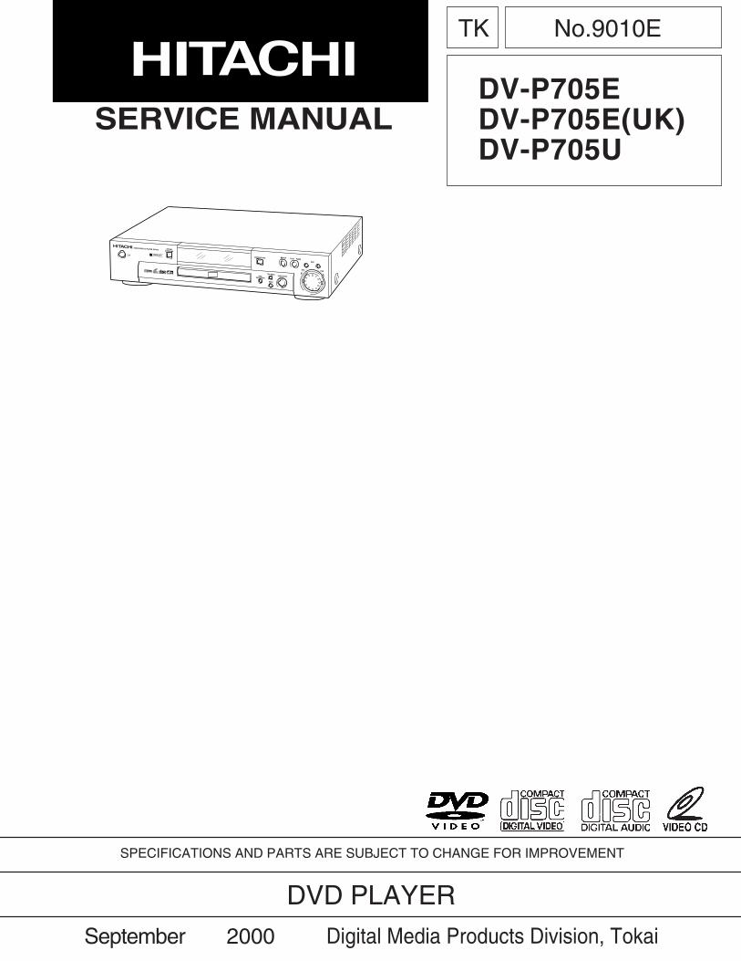
TK No.9010E
SPECIFICATIONS AND PARTS ARE SUBJECT TO CHANGE FOR IMPROVEMENT
DVD PLAYER
SERVICE MANUAL
2000September Digital Media Products Division, Tokai
DV-P705EDV-P705E(UK)DV-P705U
DVD/CD/VIDEO CD PLAYER DV-P705 VIRTUALSURROUND
OPEN/CLOSE
DISCNAVIGATION
TOP MENUPUSH ENTER
MENU
STOP
SKIP
FWDREV
PLAY/ PAUSE
/ I
PRODUCT SAFETY NOTICE Many electrical and mechanical parts have special safety-related characteristics. These are often not evident from visualinspection nor can the protection afforded by them necessarily be obtained by using replacement components rated for ahigher voltage, wattage, etc. Replacement parts which have these special safety characteristics are identified in thisService Manual. Electrical components having such features are identified by marking with a on the schematics andthe parts list in this Service Manual. The use of a substitute replacement component which does not have the samesafety characteristics as the HITACHI recommended replacement one, shown in the parts list in this Service Manual, maycreate shock, fire, or other hazards. Product safety is continuously under review and new instructions are issued fromtime to time. For the latest information, always consult the current HITACHI Service Manual. A subscription to, oradditional copies for, HITACHI Service Manual may be obtained at a nominal charge from HITACHI SALESCORPORATION.
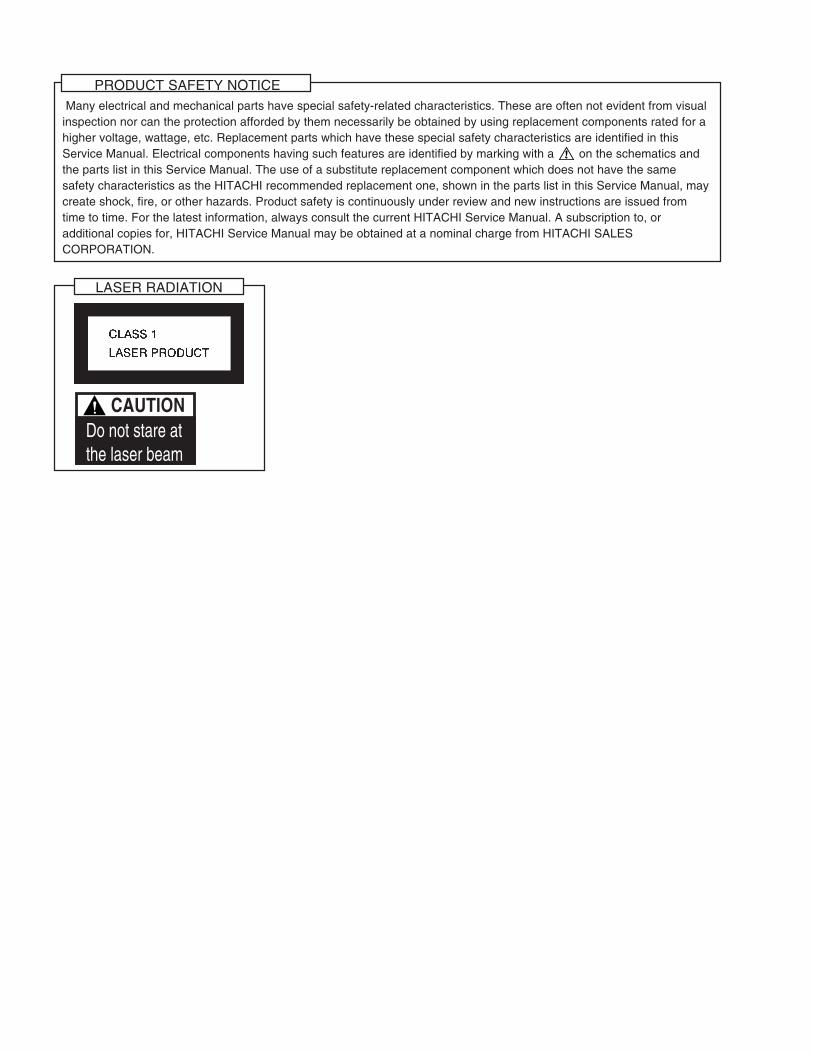
LASER RADIATION
Do not stare atthe laser beam
CAUTION
NOTICE:Comply with all cautions and safety related noteslocated on or inside the cabinet and on the chassis.
1. When replacing a chassis in the instrument, all theprotective devices must be put back in place, such asbarriers, non-metallic knobs, adjustment andcompartment covers/shields, isolation resistors/capacitors, etc.
2. When service is required, observe the original lead-ress. Extra precautions should be taken to assurecorrect lead dress in the high voltage circuit.
3. Always use the manufacturer's replacementcomponents. Especially critical components asindicated on the circuit diagram should not bereplaced by other manufacturer's. Furthermore,where a short-circuit has occurred, replace thosecomponents that indicate evidence of overheating.
4. Before returning an instrument to the customer, theservice technician must thoroughly test the unit to becertain that it is completely safe to operate withoutdanger of electrical shock, and be sure that noprotective device built into the instrument by themanufacturer has become defective or inadvertentlydefeated during servicing. Therefore, the followingchecks should be performed for the continuedprotection of the customer and service technician.
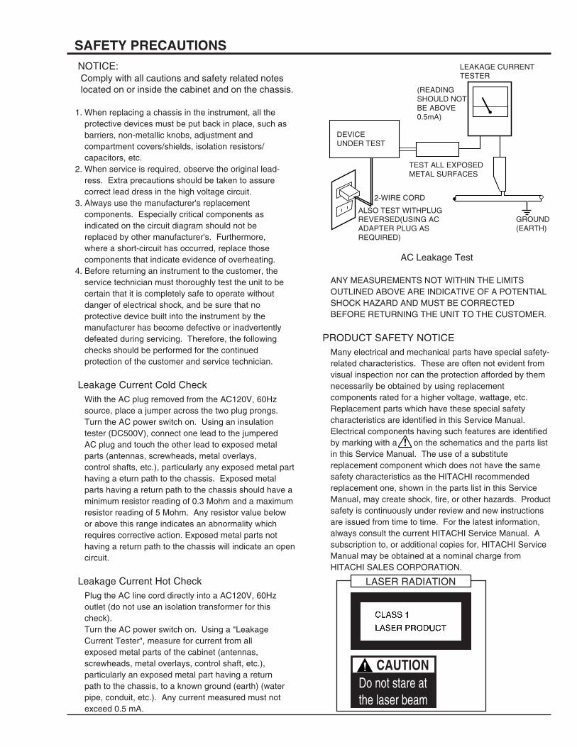
Leakage Current Cold CheckWith the AC plug removed from the AC120V, 60Hzsource, place a jumper across the two plug prongs.Turn the AC power switch on. Using an insulationtester (DC500V), connect one lead to the jumperedAC plug and touch the other lead to exposed metalparts (antennas, screwheads, metal overlays,control shafts, etc.), particularly any exposed metal parthaving a eturn path to the chassis. Exposed metalparts having a return path to the chassis should have aminimum resistor reading of 0.3 Mohm and a maximumresistor reading of 5 Mohm. Any resistor value belowor above this range indicates an abnormality whichrequires corrective action. Exposed metal parts nothaving a return path to the chassis will indicate an opencircuit.
Leakage Current Hot CheckPlug the AC line cord directly into a AC120V, 60Hzoutlet (do not use an isolation transformer for thischeck).Turn the AC power switch on. Using a "LeakageCurrent Tester", measure for current from allexposed metal parts of the cabinet (antennas,screwheads, metal overlays, control shaft, etc.),particularly an exposed metal part having a returnpath to the chassis, to a known ground (earth) (waterpipe, conduit, etc.). Any current measured must notexceed 0.5 mA.
SAFETY PRECAUTIONS
AC Leakage Test
ANY MEASUREMENTS NOT WITHIN THE LIMITSOUTLINED ABOVE ARE INDICATIVE OF A POTENTIALSHOCK HAZARD AND MUST BE CORRECTEDBEFORE RETURNING THE UNIT TO THE CUSTOMER.
PRODUCT SAFETY NOTICEMany electrical and mechanical parts have special safety-related characteristics. These are often not evident fromvisual inspection nor can the protection afforded by themnecessarily be obtained by using replacementcomponents rated for a higher voltage, wattage, etc.Replacement parts which have these special safetycharacteristics are identified in this Service Manual.Electrical components having such features are identifiedby marking with a on the schematics and the parts listin this Service Manual. The use of a substitutereplacement component which does not have the samesafety characteristics as the HITACHI recommendedreplacement one, shown in the parts list in this ServiceManual, may create shock, fire, or other hazards. Productsafety is continuously under review and new instructionsare issued from time to time. For the latest information,always consult the current HITACHI Service Manual. Asubscription to, or additional copies for, HITACHI ServiceManual may be obtained at a nominal charge fromHITACHI SALES CORPORATION.
DEVICEUNDER TEST
(READINGSHOULD NOTBE ABOVE0.5mA)
LEAKAGE CURRENTTESTER
TEST ALL EXPOSEDMETAL SURFACES
2-WIRE CORD
ALSO TEST WITHPLUGREVERSED(USING ACADAPTER PLUG ASREQUIRED)
GROUND(EARTH)
LASER RADIATION
Do not stare atthe laser beam
CAUTION
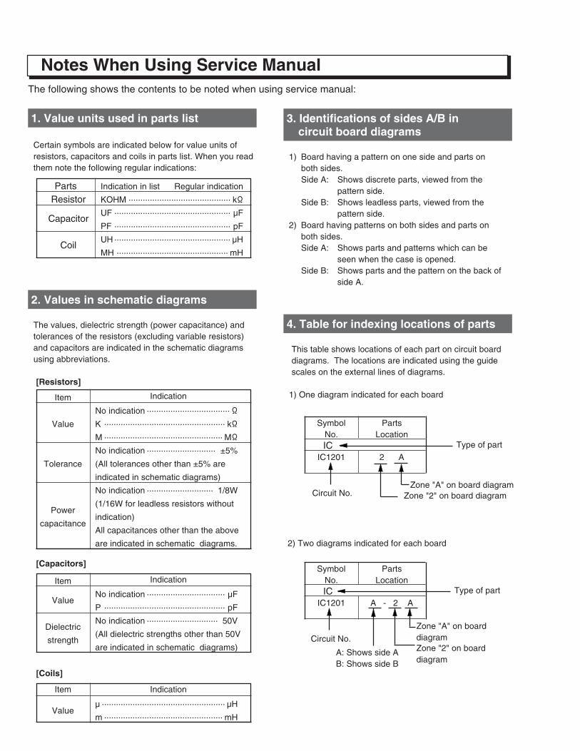
Notes When Using Service ManualThe following shows the contents to be noted when using service manual:
1. Value units used in parts list
This table shows locations of each part on circuit boarddiagrams. The locations are indicated using the guidescales on the external lines of diagrams.
1) One diagram indicated for each board
The values, dielectric strength (power capacitance) andtolerances of the resistors (excluding variable resistors)and capacitors are indicated in the schematic diagramsusing abbreviations.
[Resistors]
Certain symbols are indicated below for value units ofresistors, capacitors and coils in parts list. When you readthem note the following regular indications:
Indication in list Regular indication
KOHM ........................................... k
UF ................................................. µF
PF ................................................. pF
UH ................................................. µH
MH ............................................... mH
PartsResistor
Capacitor
Coil
2) Two diagrams indicated for each board
2. Values in schematic diagrams
Item
Value
Tolerance
Power
capacitance
Indication
No indication ...................................
K ................................................... k
M .................................................. M
No indication ............................. ±5%
(All tolerances other than ±5% are
indicated in schematic diagrams)
No indication ............................ 1/8W
(1/16W for leadless resistors without
indication)
All capacitances other than the above
are indicated in schematic diagrams.
[Capacitors]
Item
Value
Dielectric
strength
Indication
No indication ................................. µF
P ................................................... pF
No indication .............................. 50V
(All dielectric strengths other than 50V
are indicated in schematic diagrams)
Item
Value
Indication
µ .................................................... µH
m .................................................. mH
[Coils]
3. Identifications of sides A/B incircuit board diagrams
1) Board having a pattern on one side and parts onboth sides.Side A: Shows discrete parts, viewed from the
pattern side.Side B: Shows leadless parts, viewed from the
pattern side.2) Board having patterns on both sides and parts on
both sides.Side A: Shows parts and patterns which can be
seen when the case is opened.Side B: Shows parts and the pattern on the back of
side A.
4. Table for indexing locations of parts
PartsLocation
2 A
SymbolNo.IC
IC1201
Type of part
Zone "A" on board diagramCircuit No. Zone "2" on board diagram
PartsLocation
A - 2 A
SymbolNo.IC
IC1201
Zone "2" on boarddiagram
A: Shows side AB: Shows side B
Zone "A" on boarddiagram
Type of part
Circuit No.
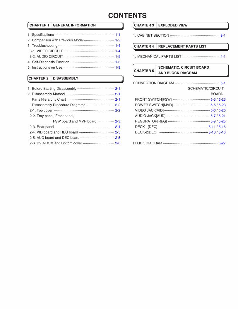
CONTENTS CHAPTER 1 GENERAL INFORMATION
1. Specifications ............................................................. 1-1
2. Comparison with Previous Model ............................... 1-2
3. Troubleshooting .......................................................... 1-4
3-1. VIDEO CIRCUIT .................................................... 1-4
3-2. AUDIO CIRCUIT .................................................... 1-5
4. Self-Diagnosis Function ............................................. 1-6
5. Instructions on Use ..................................................... 1-9
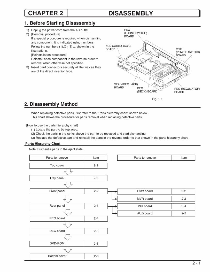
CHAPTER 2 DISASSEMBLY
1. Before Starting Disassembly ...................................... 2-1
2. Disassembly Method .................................................. 2-1
Parts Hierarchy Chart ................................................. 2-1
Disassembly Procedure Diagrams ............................. 2-2
2-1. Top cover .............................................................. 2-2
2-2. Tray panel, Front panel,
FSW board and MVR board ................. 2-3
2-3. Rear panel ............................................................. 2-4
2-4. VID board and REG board .................................... 2-5
2-5. AUD board and DEC board ................................... 2-5
2-6. DVD-ROM and Bottom cover ................................ 2-6
CHAPTER 3 EXPLODED VIEW
1. CABINET SECTION ................................................... 3-1
CHAPTER 4 REPLACEMENT PARTS LIST
1. MECHANICAL PARTS LIST ...................................... 4-1
SCHEMATIC, CIRCUIT BOARDCHAPTER 5
AND BLOCK DIAGRAM
CONNECTION DIAGRAM .............................................. 5-1
SCHEMATIC/CIRCUIT
BOARD
FRONT SWITCH[FSW] ...................................... 5-3 / 5-23
POWER SWITCH[MVR] ..................................... 5-5 / 5-23
VIDEO JACK[VID] ............................................... 5-6 / 5-20
AUDIO JACK[AUD] ............................................. 5-7 / 5-21
REGURATOR[REG] ........................................... 5-9 / 5-25
DECK-1[DEC] .................................................. 5-11 / 5-16
DECK-2[DEC] .................................................. 5-13 / 5-16
BLOCK DIAGRAM ........................................................ 5-27
1 - 1
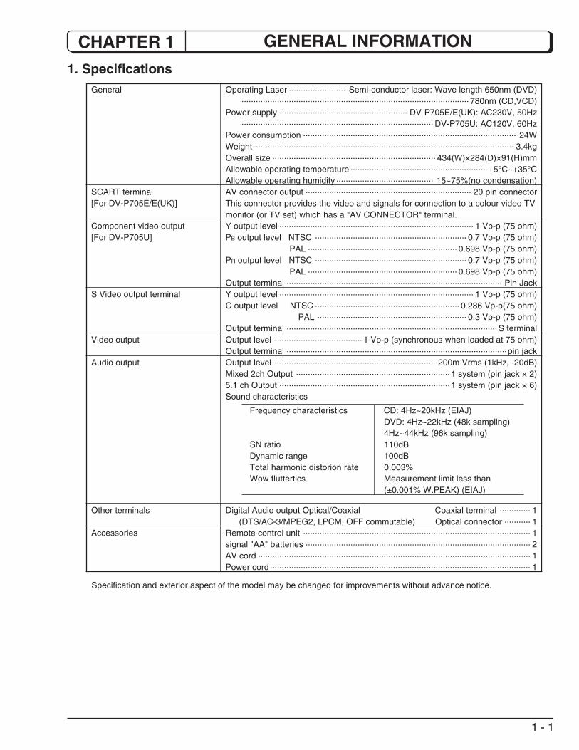
CHAPTER 1 GENERAL INFORMATION
General
SCART terminal[For DV-P705E/E(UK)]
Component video output[For DV-P705U]
S Video output terminal
Video output
Audio output
Other terminals
Accessories
1. Specifications
Specification and exterior aspect of the model may be changed for improvements without advance notice.
Operating Laser ........................ Semi-conductor laser: Wave length 650nm (DVD)................................................................................................ 780nm (CD,VCD)
Power supply ...................................................... DV-P705E/E(UK): AC230V, 50Hz................................................................................. DV-P705U: AC120V, 60Hz
Power consumption .......................................................................................... 24WWeight .............................................................................................................. 3.4kgOverall size ..................................................................... 434(W)×284(D)×91(H)mmAllowable operating temperature ......................................................... +5°C~+35°CAllowable operating humidity ......................................... 15~75%(no condensation)AV connector output ...................................................................... 20 pin connectorThis connector provides the video and signals for connection to a colour video TVmonitor (or TV set) which has a "AV CONNECTOR" terminal.Y output level .................................................................................. 1 Vp-p (75 ohm)PB output level NTSC ................................................................ 0.7 Vp-p (75 ohm) PAL ............................................................... 0.698 Vp-p (75 ohm)PR output level NTSC ................................................................ 0.7 Vp-p (75 ohm) PAL ............................................................... 0.698 Vp-p (75 ohm)Output terminal ........................................................................................... Pin JackY output level .................................................................................. 1 Vp-p (75 ohm)C output level NTSC ............................................................. 0.286 Vp-p(75 ohm)
PAL ............................................................... 0.3 Vp-p (75 ohm)Output terminal ......................................................................................... S terminalOutput level ..................................... 1 Vp-p (synchronous when loaded at 75 ohm)Output terminal .............................................................................................pin jackOutput level .................................................................... 200m Vrms (1kHz, -20dB)Mixed 2ch Output ................................................................. 1 system (pin jack × 2)5.1 ch Output ........................................................................1 system (pin jack × 6)Sound characteristics
Digital Audio output Optical/Coaxial Coaxial terminal ............. 1(DTS/AC-3/MPEG2, LPCM, OFF commutable) Optical connector ........... 1
Remote control unit ................................................................................................ 1signal "AA" batteries ............................................................................................... 2AV cord ................................................................................................................... 1Power cord .............................................................................................................. 1
Frequency characteristics CD: 4Hz~20kHz (EIAJ)DVD: 4Hz~22kHz (48k sampling)4Hz~44kHz (96k sampling)
SN ratio 110dBDynamic range 100dBTotal harmonic distorion rate 0.003%Wow fluttertics Measurement limit less than
(±0.001% W.PEAK) (EIAJ)
1 - 2
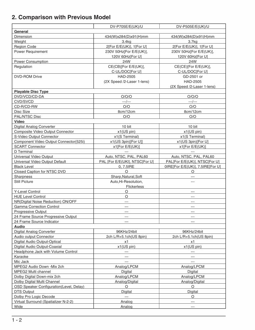
2. Comparison with Previous ModelDV-P705E/E(UK)/U DV-P505E/E(UK)/U
GeneralDimension 434(W)x284(D)x91(H)mm 434(W)x284(D)x91(H)mmWeight 3.4kg 3.7kgRegion Code 2[For E/E(UK)], 1[For U] 2[For E/E(UK)], 1[For U]Power Requirement 230V 50Hz[For E/E(UK)], 230V 50Hz[For E/E(UK)],
120V 60Hz[For U] 120V 60Hz[For U]Power Consumption 24W 24WRegulation CE(CB)[For E/E(UK)], CE(CE)[For E/E(UK)],
C-UL/DOC[For U] C-UL/DOC[For U]DVD-ROM Drive HAD-2505 GD-2501 or
(2X Speed /2-Laser 1-lens) HAD-2505(2X Speed /2-Laser 1-lens)
Playable Disc TypeDVD/VCD/CD-DA O/O/O O/O/OCVD/SVCD ---/--- ---/---CD-R/CD-RW O/O O/ODisc Size 8cm/12cm 8cm/12cmPAL/NTSC Disc O/O O/OVideoDigital Analog Converter 10 bit 10 bitComposite Video Output Connector x1(US pin) x1(US pin)S-Video Output Connector x1(S Terminal) x1(S Terminal)Component Video Output Connector(525i) x1(US 3pin)[For U]] x1(US 3pin)[For U]SCART Connector x1[For E/E(UK)] x1[For E/E(UK)]D Terminal --- ---Universal Video Output Auto, NTSC, PAL, PAL60 Auto, NTSC, PAL, PAL60Universal Video Output Default PAL [For E/E(UKI], NTSC[For U] PAL[For E/E(UK)], NTSC[For U]Black Level 0, 7.5IRE 0IRE[For E/E(UK)], 7.5IRE[For U]Closed Caption for NTSC DVD O OSharpness Sharp,Natural,Soft ---Still Picture Auto,Hi-Resolution, ---
FlickerlessY-Level Control O ---HUE Level Control O ---NR(Digital Noise Reduction) ON/OFF --- ---Gamma Correction Control --- ---Progressive Output --- ---24 Frame Source Progressive Output --- ---24 Frame Source Indicator --- ---AudioDigital Analog Converter 96KHz/24bit 96KHz/24bitAudio output Connector 2ch L/R+5.1ch(US 8pin) 2ch L/R+5.1ch(US 8pin)Digital Audio Output-Optical x1 x1Digital Audio Output-Coaxial x1(US pin) x1(US pin)Headphone Jack with Volume Control --- ---Karaoke --- ---Mic Jack --- ---MPEG2 Audio Down -Mix 2ch Analog/LPCM Analog/LPCMMPEG2 Multi channel Digital DigitalDolby Digital Down-mix 2ch Analog/LPCM Analog/LPCMDolby Digital Multi Channel Analog/Digital Analog/DigitalOSD Speaker Configuration(Level, Delay) O ODTS Output Digital DigitalDolby Pro Logic Decode --- OVirtual Surround (Spatializer N-2-2) Analog ---Wide Analog ---
1 - 3
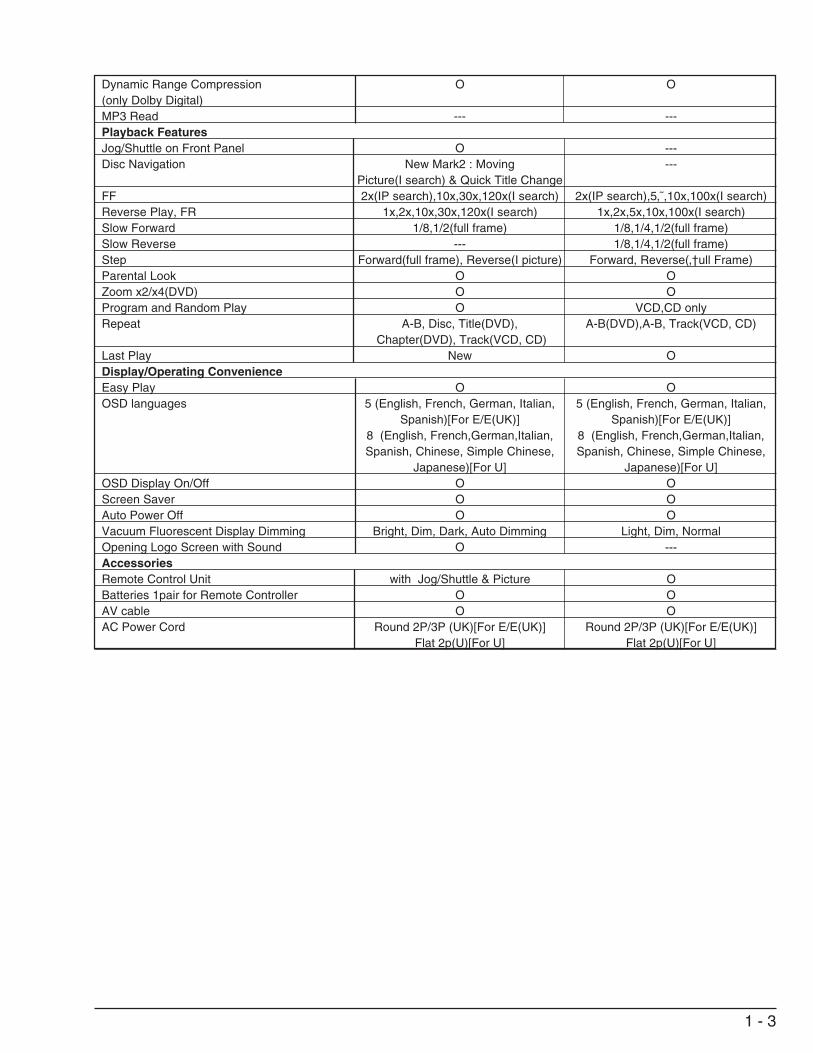
Dynamic Range Compression O O(only Dolby Digital)MP3 Read --- ---Playback FeaturesJog/Shuttle on Front Panel O ---Disc Navigation New Mark2 : Moving ---
Picture(I search) & Quick Title ChangeFF 2x(IP search),10x,30x,120x(I search) 2x(IP search),5‚˜,10x,100x(I search)Reverse Play, FR 1x,2x,10x,30x,120x(I search) 1x,2x,5x,10x,100x(I search)Slow Forward 1/8,1/2(full frame) 1/8,1/4,1/2(full frame)Slow Reverse --- 1/8,1/4,1/2(full frame)Step Forward(full frame), Reverse(I picture) Forward, Reverse(‚†ull Frame)Parental Look O OZoom x2/x4(DVD) O OProgram and Random Play O VCD,CD onlyRepeat A-B, Disc, Title(DVD), A-B(DVD),A-B, Track(VCD, CD)
Chapter(DVD), Track(VCD, CD)Last Play New ODisplay/Operating ConvenienceEasy Play O OOSD languages 5 (English, French, German, Italian, 5 (English, French, German, Italian,
Spanish)[For E/E(UK)] Spanish)[For E/E(UK)]8 (English, French,German,Italian, 8 (English, French,German,Italian,Spanish, Chinese, Simple Chinese, Spanish, Chinese, Simple Chinese,
Japanese)[For U] Japanese)[For U]OSD Display On/Off O OScreen Saver O OAuto Power Off O OVacuum Fluorescent Display Dimming Bright, Dim, Dark, Auto Dimming Light, Dim, NormalOpening Logo Screen with Sound O ---AccessoriesRemote Control Unit with Jog/Shuttle & Picture OBatteries 1pair for Remote Controller O OAV cable O OAC Power Cord Round 2P/3P (UK)[For E/E(UK)] Round 2P/3P (UK)[For E/E(UK)]
Flat 2p(U)[For U] Flat 2p(U)[For U]
1 - 4
3. Troubleshooting
3-1. VIDEO CIRCUIT
ARE SIGNALSOUTPUT FROM VIDEOOUTPUT TERMINAL?
Yes
No
CHECK SIGNALCABLE/ MONITOR
CHECK VIDEO OUTPUTSECTOR (PG1302/ J1307/ J1302/ J1306/ J1361) OF JAK PWB
CHECK IC3301/ IC3302 of JAK PWB
CHECK IC1201/ IC1101/ IC1601
CHECK POWER SUPPLY CIRCUIT
CHECK IC1601
CHECK X2201/ R1218
REPLACE IC2202
ARE SIGNALSOUTPUT FROM PG2201pins 17, 15, 13, 11, 9, 7,
3?
ARE SIGNALS IC2202 pins
14, 15, 16, 20, 21?
+5V AT IC2202pins 46, 34, 32, 30, 27,
19, 11, 1 (VDD)?
IS VOLTAGE ATIC2202 pins 44
(RESET) H LEVEL?
IS CLOCK INIC2202 pin 48?
Yes
No
Yes
No
No
Yes
No
Yes
No
Yes
No
Yes
ARE SIGNALSOUTPUT FROM
IC2202 pins 35, 33, 29, 28, 25, 24?
NO IMAGE
1 - 5
IS THEREAN IMAGE?
No
Yes
BREAKDOWN BEFORE IC1201
CHECK IC1506 OR +8V LINE ETC.
CHECK IC1101/ IC1601
BREAKDOWN OF Q1505 OR Q1506 OR D1504
BREAKDOWN OF IC1501, IC1507
ARE IC1501pins 8, 9, 15, 20
5V?
ARE THERE SIGNALS AT IC1501
PINS 13, 16 and IC1507 pins 9-14?
IS Q1505BASE VOLTAGE
0V?
IS Q1505COLLECTOR
VOLTAGE8V?
IS IC1501 pin 21and IC1507 pin 3-6
VOLTAGE 5V?
No
Yes
No
Yes
No
Yes
No
Yes
No
Yes
No
Yes
ARE THERE SIGNALS AT IC1501 pins 1, 2, 3, 5 AND
IC1507 pins 40, 41, 45, 46, 47, 38?
NO SOUND
IS Q1507, Q1501COLLECTOR VOLTAGE 8V?
Yes
ARE SIGNALS ATIC1507-IC1514
pins 7, 8?
Yes
BREAKDOWN OF Q1306-Q1311, Q3503, Q3504
No
BREAKDOWN OF IC1201
BREAKDOWN OF IC1506
Yes
ARE IC1506 pin 3 +5V & pin 1 +8V
ARE THERE SIGNALS AT IC1501
pins 26,27,28 andIC1507 pins 34, 35, 36?
BREAKDOWN OF IC1501
No
BREAKDOWN OF Q1507, Q1501No
BREAKDOWN OF IC1507-IC1514
No
3-2. AUDIO CIRCUIT
1 - 6
1. OverviewThis DVD player has two types of self-diagnosis function for differing operation methods:(1) Self-diagnosis started automatically when power is turned on(2) Self-diagnosis activated when test mode is selected by pressing buttons on player
2. Conditions for engaging self-diagnosisThe following conditions must be satisfied to start and complete self-diagnosis:(1) No disc loaded.(2) Power cord unplugged after self-diagnosis is complete.
3. Operation methods and diagnosis items3.1 Self-diagnosis started automatically when power is turned on(1) ATAPI bus not yet connectedIf DVD-ROM drive is not connected, “Err 0009” will appear in the display of player.Unplug the power cord and check the connection of ATAPI cable.(2) When program is not yet stored in flash memory on DEC board:Tray will open, close and then open.Unplug the power cord and check the DEC board.
3.2 Self-diagnosis engaged by pressing the buttons on player3.2.1 Simultaneously hold down the SKIP >> and POWER buttons on player for 5 seconds, and then press the PLAY button.The player will enter the automatic DEC board self-diagnosis mode.If the DEC board is normal, “0001” will appear in the display for 2 seconds, and then “0002” for 2 seconds: This indication willbe repeated.If error is detected, “Err 01” or “Err 02” will appear.
Err 01: R/W error, 4 Mbit connected to SHErr 02: R/W error, 32 Mbit connected to ZIVA
Self-diagnosis will stop when it first detects error.That is, if “Err 01” is displayed, item for “Err 002” will not be diagnosed.
3.2.2 Simultaneously hold down the << SKIP and POWER buttons on player for 5 seconds.The player will enter the selective DEC board self-diagnosis mode.When this mode is entered, the appropriate menu should appear on the TV screen.If this screen does not appear, there is a problem in the display system: Carefully check the circuits related to video encoder.
To change diagnosis items, while holding down the SKIP << button on player, press the POWER button.The following describes each diagnosis item:(1) VIDEO DACIf the TEST MENU screen appears, this item is judged normal.Indication in display: 10 00010(2) BUTTON CODEThe codes of buttons on remote control and player will appear in the display.Indication in display: 20 ***** (*****: 5-digit button code)(However, the codes of POWER button and a simultaneously pressed button are excluded.)
4. Self-Diagnosis Function
TEST MENU
VIDEO DACBUTTON CODECOLOR BARAUDIO DAC FL FR C SL SR SUBSTRING TEST
1 - 7
The codes of buttons with the same functions are identical:PLAY/PAUSE : 10104SKIP >> : 00002SKIP << : 00003STOP : 00111OPEN : 00009DISPLAY : 00011
The codes of jog and shuttle are as follows:
(3) COLOR BARThe color bar will appear.Each time SKIP >> is pressed, the following display conditions will be established in sequence:1) NTSC standard playback (Y, Pb, Pr)Indication in display: 30 00002) NTSC Letterbox displayIndication in display: 30 00013) NTSC Squeeze displayIndication in display: 30 00024) PAL50 (RGB on) Squeeze displayIndication in display: 30 00035) PAL (RGB on) standard playbackIndication in display: 30 0004Pressing SKIP >> at this time will return to 1).
(4) AUDIO DACWhite noise is output from each audio channel.Indication in display: 40Each time SKIP >> is pressed, the audio output channel will switch as follows:FL -> FR -> C -> SL -> SR -> SUB -> FL -> ...Each time SKIP << is pressed, the audio output channel will switch as follows:SUB -> SR -> SL -> C -> FR -> FL -> SUB -> ...
(5) STRING TESTThe on-screen information (OSD) used by DVD player is displayed.Indication in display: 50Each time SKIP >> is pressed, the contents of string will switch as follows:OPEN -> CLOSE -> PLAY -> STOP -> PAUSE -> TITLE -> CHAPTER -> ...Each time SKIP << is pressed, the contents of string will switch as follows:CHAPTER -> TITLE -> PAUSE -> STOP -> PLAY -> CLOSE -> OPEN -> ...
Jog dial Indication in player displayForward 10500
Backward 10501
Shuttle position -7 -6 -5 -4 -3 -2 -1 0 0 +1 +2 +3 +4 +5 +6 +7Indication in
00414 00404 00400 00403 00413player display
1 - 8
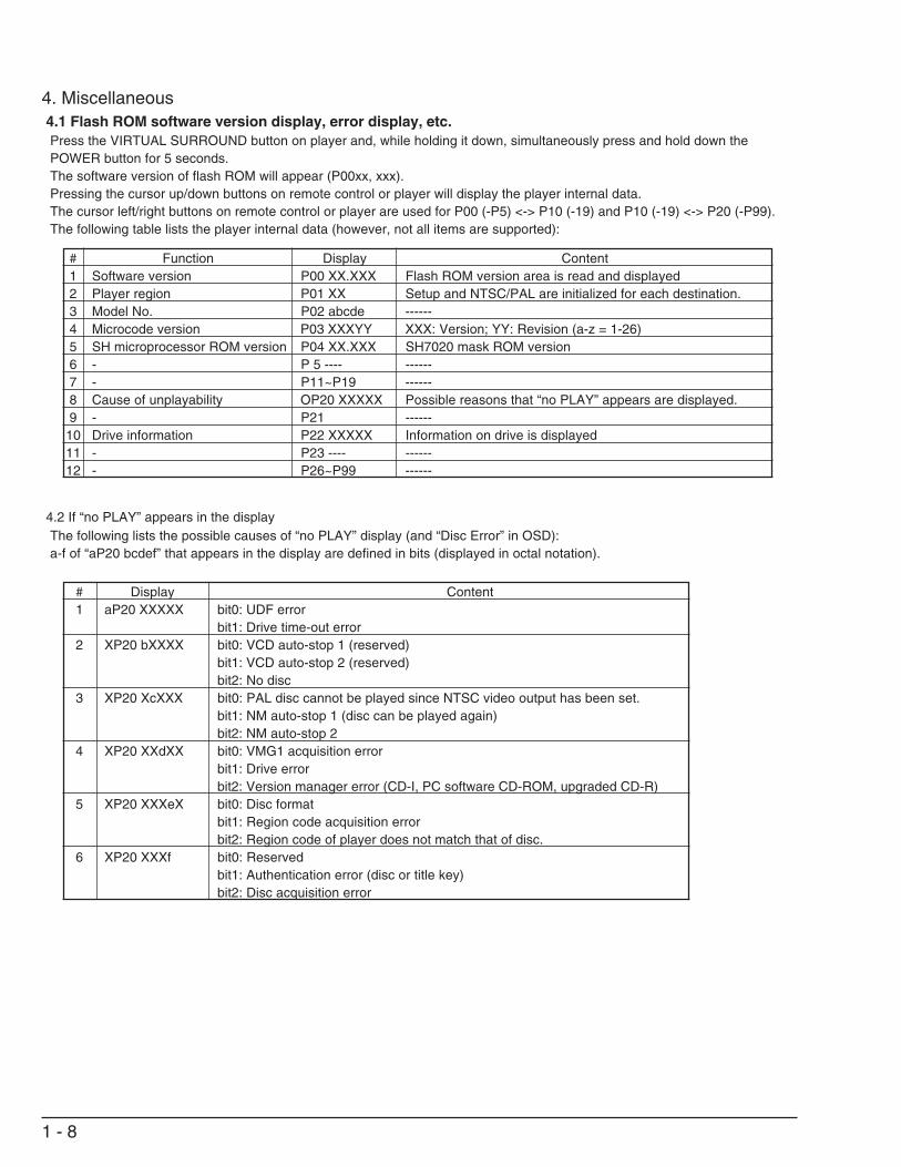
4. Miscellaneous4.1 Flash ROM software version display, error display, etc.Press the VIRTUAL SURROUND button on player and, while holding it down, simultaneously press and hold down thePOWER button for 5 seconds.The software version of flash ROM will appear (P00xx, xxx).Pressing the cursor up/down buttons on remote control or player will display the player internal data.The cursor left/right buttons on remote control or player are used for P00 (-P5) <-> P10 (-19) and P10 (-19) <-> P20 (-P99).The following table lists the player internal data (however, not all items are supported):
4.2 If “no PLAY” appears in the displayThe following lists the possible causes of “no PLAY” display (and “Disc Error” in OSD):a-f of “aP20 bcdef” that appears in the display are defined in bits (displayed in octal notation).
# Function Display Content1 Software version P00 XX.XXX Flash ROM version area is read and displayed2 Player region P01 XX Setup and NTSC/PAL are initialized for each destination.3 Model No. P02 abcde ------4 Microcode version P03 XXXYY XXX: Version; YY: Revision (a-z = 1-26)5 SH microprocessor ROM version P04 XX.XXX SH7020 mask ROM version6 - P 5 ---- ------7 - P11~P19 ------8 Cause of unplayability OP20 XXXXX Possible reasons that “no PLAY” appears are displayed.9 - P21 ------10 Drive information P22 XXXXX Information on drive is displayed11 - P23 ---- ------12 - P26~P99 ------
# Display Content1 aP20 XXXXX bit0: UDF error
bit1: Drive time-out error2 XP20 bXXXX bit0: VCD auto-stop 1 (reserved)
bit1: VCD auto-stop 2 (reserved)bit2: No disc
3 XP20 XcXXX bit0: PAL disc cannot be played since NTSC video output has been set.bit1: NM auto-stop 1 (disc can be played again)bit2: NM auto-stop 2
4 XP20 XXdXX bit0: VMG1 acquisition errorbit1: Drive errorbit2: Version manager error (CD-I, PC software CD-ROM, upgraded CD-R)
5 XP20 XXXeX bit0: Disc formatbit1: Region code acquisition errorbit2: Region code of player does not match that of disc.
6 XP20 XXXf bit0: Reservedbit1: Authentication error (disc or title key)bit2: Disc acquisition error
1 - 9
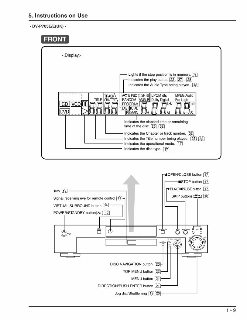
5. Instructions on Use
- DV-P705E/E(UK) -
DISC NAVIGATION button
Signal receiving eye for remote control
Tray
POWER/STANDBY button( )
MENU button
SKIP buttons( )
STOP button
PLAY/ PAUSE button
VIRTUAL SURROUND button
OPEN/CLOSE button
TOP MENU button
17
17
34
21
18
22
17
17
11
17
23
DIRECTION/PUSH ENTER button 21
Jog dial/Shuttle ring 19 20
PUSH ENTERTOP MENU
MENU
DISCNAVIGATION
SKIPSTOP PAUSEPLAY/OPEN/CLOSEVIRTUAL
SURROUND
REV FWD
FRONT
<Display>
21
32
27 28
42
2517
32
25
32
17Indicates the disc type.Indicates the operational mode.Indicates the Title number being played. ,Indicates the Chapter or track number.
Indicates the elapsed time or remaining time of the disc. ,
Indicates the Audio Type being played.Indicates the play status. , ~
Lights if the stop position is in memory.22
A B PBC ((( SR ))) RANDOM ANGLE PROGRAMLAST TOTAL REMAIN
CD
DVD
LPCM dtsDolby Digital
MPEG AudioPro LogicTITLE
H M
kHz bit
S
TRACKCHAPTER
VCD
1 - 10
1 2 3
4 5 6
7 8 9
0CLEAR
DISPLAY
ANGLE SUBTITLE AUDIO SURROUND
DIRECTSEARCH
STEP
ZOOM
TOP MENU
MENU
RETURN
LAST
– SPEED +
SETUP
PICTURE A–B
OPEN/CLOSE/ I
PLAY/PAUSE
STOP
DISC NAVIGATION
ENTER
REV FWD
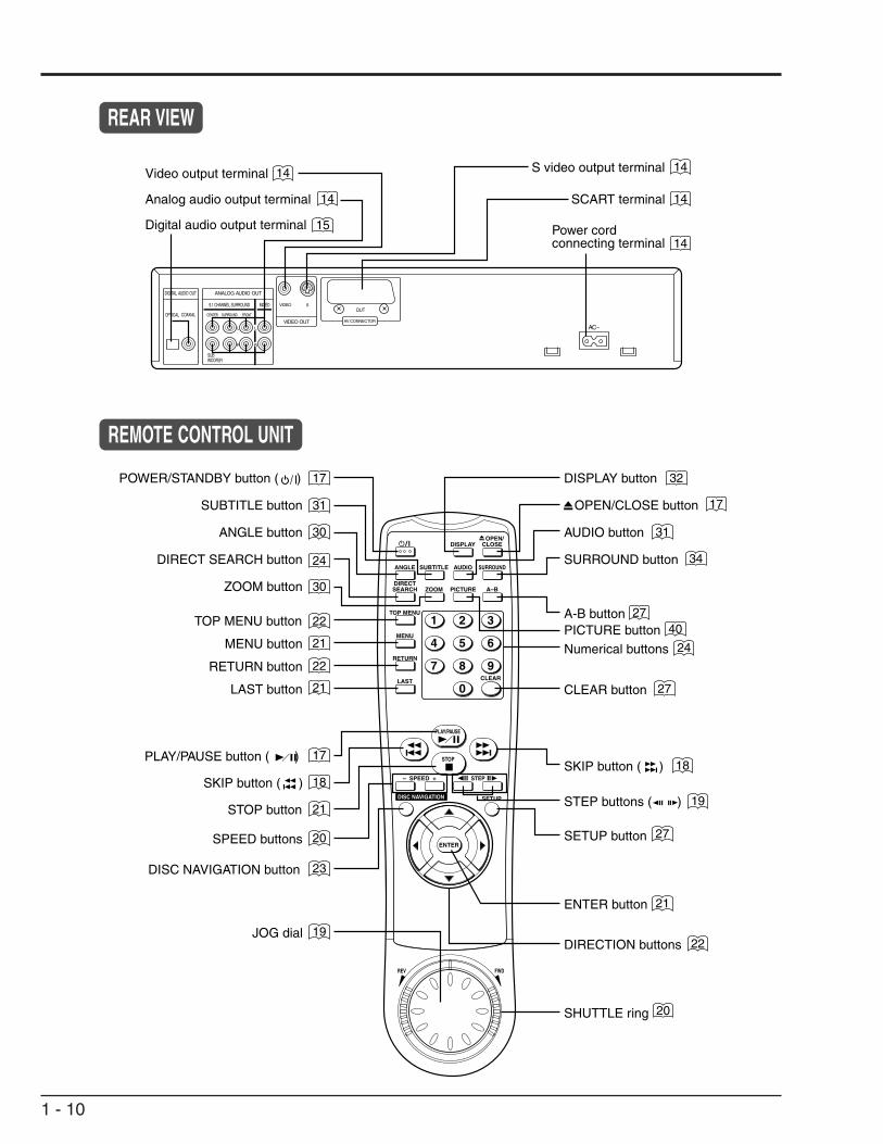
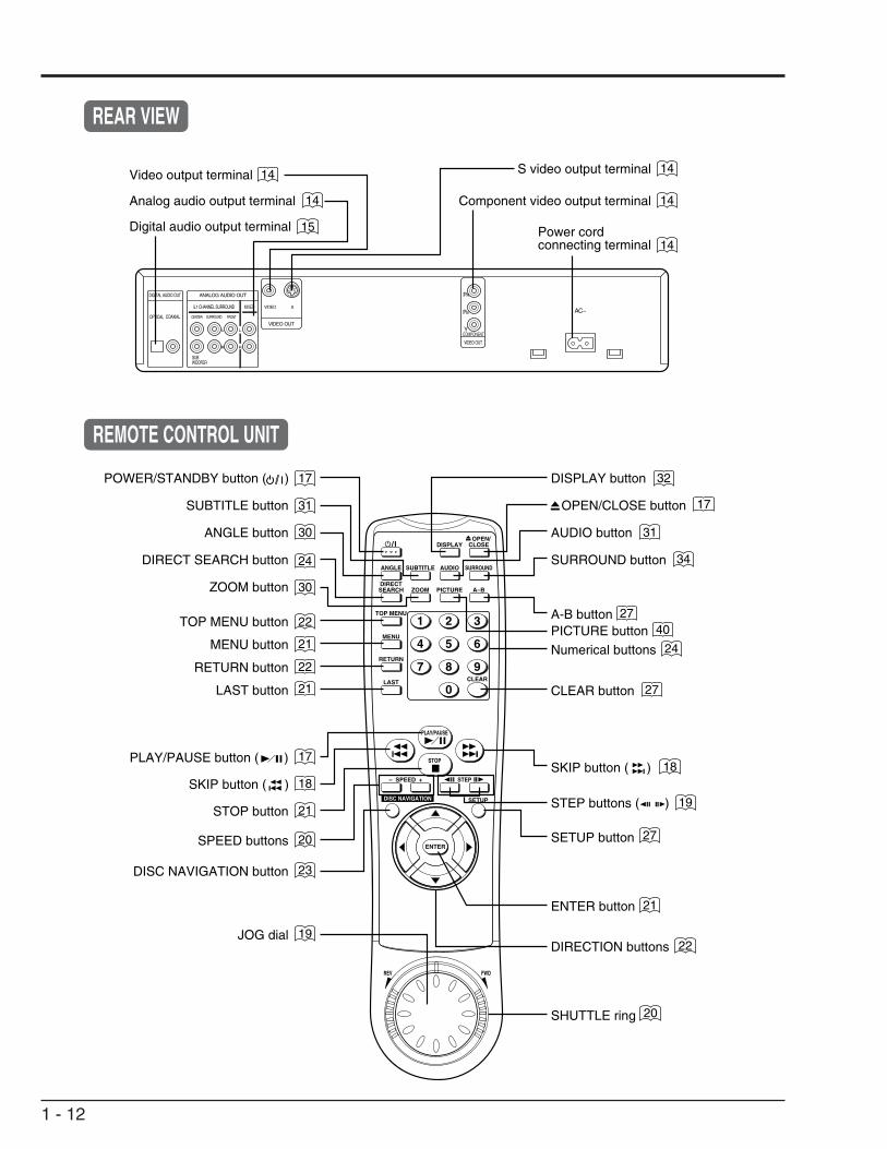
DISPLAY button
OPEN/CLOSE button
AUDIO button
SURROUND button
PICTURE button
SKIP button ( )
STEP buttons ( )
POWER/STANDBY button ( )
SUBTITLE button
ANGLE button
DIRECT SEARCH button
ZOOM button
TOP MENU button
PLAY/PAUSE button ( )
JOG dial
A-B button
Numerical buttons
CLEAR button
SETUP button
DIRECTION buttons
ENTER button
SHUTTLE ring
SKIP button ( )
STOP button
SPEED buttons
DISC NAVIGATION button
MENU button
RETURN button
LAST button
17 32
17
31
34
27
24
40
27
18
27
21
22
20
31
30
30
22
21
17
18
21
20
23
19
21
22
24
19
REAR VIEW
REMOTE CONTROL UNIT
Digital audio output terminal
Analog audio output terminal
Video output terminal S video output terminal
SCART terminal
Power cordconnecting terminal
14
1414
14
15
14
AC~
DIGITAL AUDIO OUT ANALOG AUDIO OUT
COAXIALOPTICAL SURROUNDCENTER FRONT
SUB WOOFER
5.1 CHANNEL SURROUND
R
L
VIDEO S
VIDEO OUT
MIXED
R
L
OUT
AV CONNECTOR
1 - 11
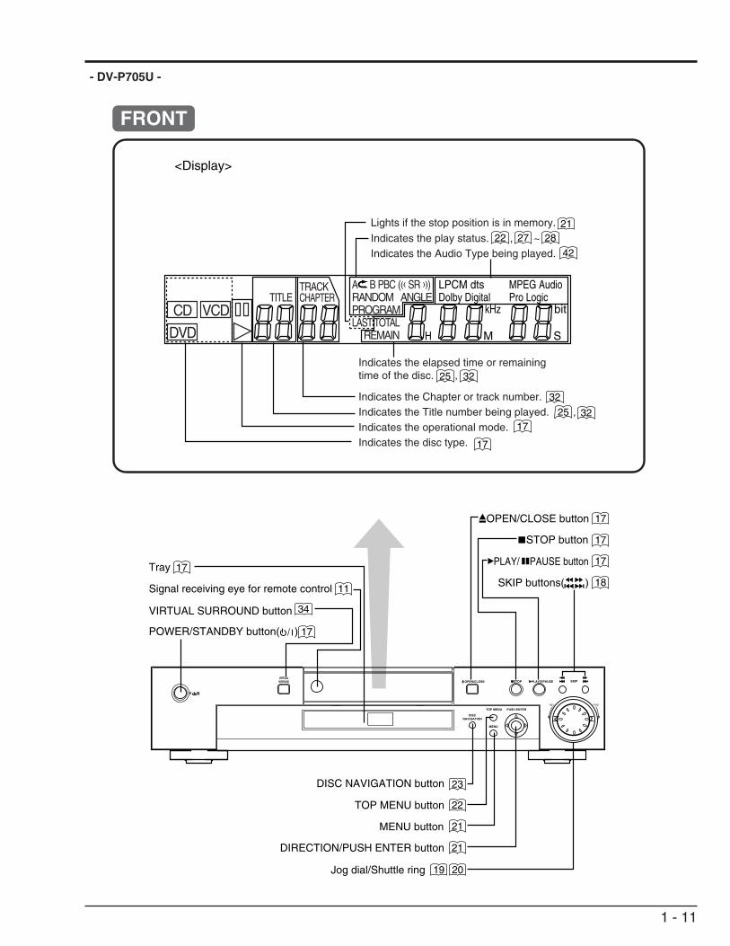
- DV-P705U -
DISC NAVIGATION button
Signal receiving eye for remote control
Tray
POWER/STANDBY button( )
MENU button
SKIP buttons( )
STOP button
PLAY/ PAUSE button
VIRTUAL SURROUND button
OPEN/CLOSE button
TOP MENU button
17
17
34
21
18
22
17
17
11
17
23
DIRECTION/PUSH ENTER button 21
Jog dial/Shuttle ring 19 20
PUSH ENTERTOP MENU
MENU
DISCNAVIGATION
SKIPSTOP PAUSEPLAY/OPEN/CLOSEVIRTUAL
SURROUND
REV FWD
FRONT
<Display>
21
32
27 28
42
2517
32
25
32
17Indicates the disc type.Indicates the operational mode.Indicates the Title number being played. ,Indicates the Chapter or track number.
Indicates the elapsed time or remaining time of the disc. ,
Indicates the Audio Type being played.Indicates the play status. , ~
Lights if the stop position is in memory.22
A B PBC ((( SR ))) RANDOM ANGLE PROGRAMLAST TOTAL REMAIN
CD
DVD
LPCM dtsDolby Digital
MPEG AudioPro LogicTITLE
H M
kHz bit
S
TRACKCHAPTER
VCD
1 - 12
1 2 3
4 5 6
7 8 9
0CLEAR
DISPLAY
ANGLE SUBTITLE AUDIO SURROUND
DIRECTSEARCH
STEP
ZOOM
TOP MENU
MENU
RETURN
LAST
– SPEED +
SETUP
PICTURE A–B
OPEN/CLOSE/I
PLAY/PAUSE
STOP
DISC NAVIGATION
ENTER
REV FWD
DISPLAY button
OPEN/CLOSE button
AUDIO button
SURROUND button
PICTURE button
SKIP button ( )
STEP buttons ( )
POWER/STANDBY button ( )
SUBTITLE button
ANGLE button
DIRECT SEARCH button
ZOOM button
TOP MENU button
PLAY/PAUSE button ( )
JOG dial
A-B button
Numerical buttons
CLEAR button
SETUP button
DIRECTION buttons
ENTER button
SHUTTLE ring
SKIP button ( )
STOP button
SPEED buttons
DISC NAVIGATION button
MENU button
RETURN button
LAST button
17 32
17
31
34
27
24
40
27
18
27
21
22
20
31
30
30
22
21
17
18
21
20
23
19
21
22
24
19
REAR VIEW
REMOTE CONTROL UNIT
Digital audio output terminal
Analog audio output terminal
Video output terminal S video output terminal
Component video output terminal
Power cordconnecting terminal
14
1414
14
15
14
PR
PB
Y
AC~
DIGITAL AUDIO OUT ANALOG AUDIO OUT
COAXIALOPTICAL SURROUNDCENTER FRONT
SUB WOOFER
5.1 CHANNEL SURROUND
R
L
VIDEO S
VIDEO OUT
VIDEO OUT
MIXED
COMPONENT
R
L
2 - 1
Parts to remove Item
Top cover 2-1
2-2Tray panel
2-2FSW board
Parts to remove Item
2. Disassembly Method
When replacing defective parts, first refer to the "Parts hierarchy chart" shown below.This chart shows the procedure for parts removal when replacing defective parts.
[How to use the parts hierarchy chart](1) Locate the part to be replaced.(2) Check the parts in the ranks above the part to be replaced and start dismantling.(3) Replace the defective part and reinstall the parts in the reverse order to that shown in the parts hierarchy chart.
1) Unplug the power cord from the AC outlet.2) [Removal procedure]
If a special procedure is required when dismantlingany component, it is indicated using numbers.Follow the numbers (1),(2),(3) ... shown in theillustrations.[Reinstallation procedure]Reinstall each component in the reverse order toremoval when otherwise not specified.
3) Insert card connectors securely all the way as theyare of the direct insertion type.
Parts Hierarchy Chart
Note: Dismantle parts in the eject state.
1. Before Starting Disassembly
Fig. 1-1
2-2Front panel
2-4REG board
2-5DEC board
MVR(POWER SWITCH)BOARD
DVD-ROM 2-6
VID (VIDEO JACK)BOARD
CHAPTER 2 DISASSEMBLY
2-2MVR board
2-5AUD board
2-4VID board2-3Rear panel
DEC(DECK) BOARD
REG (REGULATOR)BOARD
AUD (AUDIO JACK)BOARD
FSW(FRONT SWITCH)BOARD
Bottom cover 2-6
2 - 2
Fig. 2-1
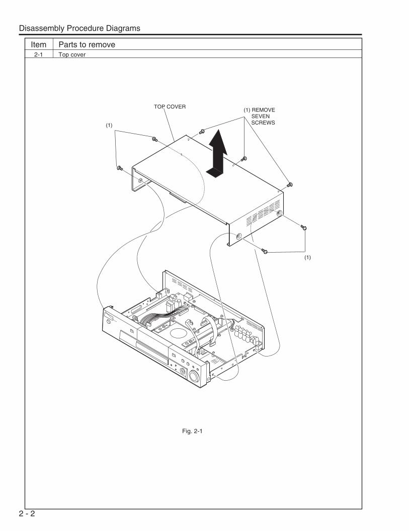
Disassembly Procedure Diagrams
Item Parts to remove2-1 Top cover
(1)
TOP COVER(1) REMOVE SEVEN SCREWS
(1)
2 - 3
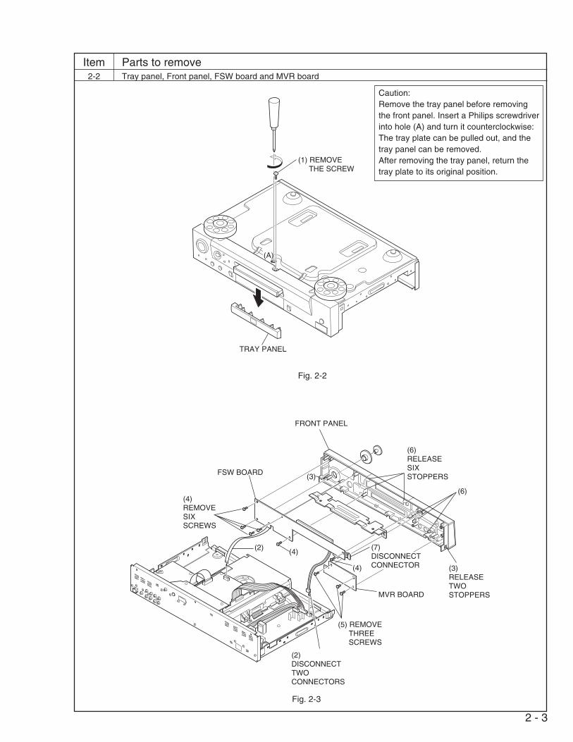
Item Parts to remove2-2 Tray panel, Front panel, FSW board and MVR board
Fig. 2-2
Fig. 2-3
(1) REMOVE THE SCREW
TRAY PANEL
(A)
FRONT PANEL
(6)RELEASESIXSTOPPERS
(3)RELEASETWOSTOPPERSMVR BOARD
(5) REMOVE THREE SCREWS
(7)DISCONNECTCONNECTOR(4)
(4)
(2)DISCONNECTTWOCONNECTORS
(2)
(4)REMOVESIXSCREWS
FSW BOARD
(6)
Caution:Remove the tray panel before removingthe front panel. Insert a Philips screwdriverinto hole (A) and turn it counterclockwise:The tray plate can be pulled out, and thetray panel can be removed.After removing the tray panel, return thetray plate to its original position.
(3)
2 - 4
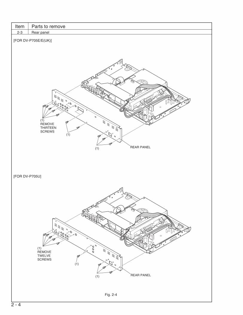
Item Parts to remove2-3 Rear panel
Fig. 2-4
(1)REMOVETHIRTEENSCREWS
(1)
(1) REAR PANEL
[FOR DV-P705U]
[FOR DV-P705E/E(UK)]
(1)REMOVETWELVESCREWS
(1)
(1) REAR PANEL
2 - 5
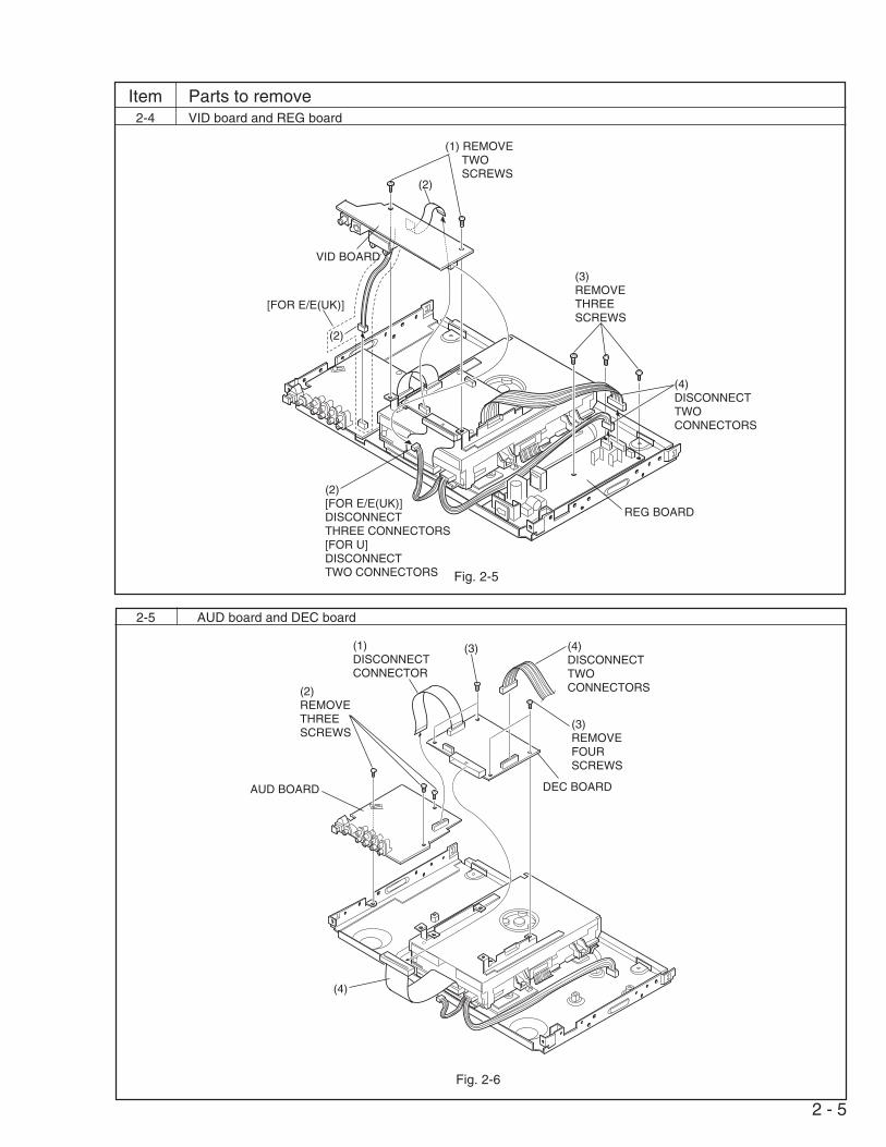
Fig. 2-6
(2)REMOVETHREESCREWS
(4)
AUD BOARD DEC BOARD
(4)DISCONNECTTWOCONNECTORS
(3)REMOVEFOURSCREWS
(1)DISCONNECTCONNECTOR
2-5 AUD board and DEC board
Fig. 2-5
(2)[FOR E/E(UK)]DISCONNECTTHREE CONNECTORS[FOR U]DISCONNECTTWO CONNECTORS
REG BOARD
(4)DISCONNECTTWOCONNECTORS
(3)REMOVETHREESCREWS
(1) REMOVE TWO SCREWS
VID BOARD
(2)
Item Parts to remove2-4 VID board and REG board
(2)
[FOR E/E(UK)]
(3)
2 - 6
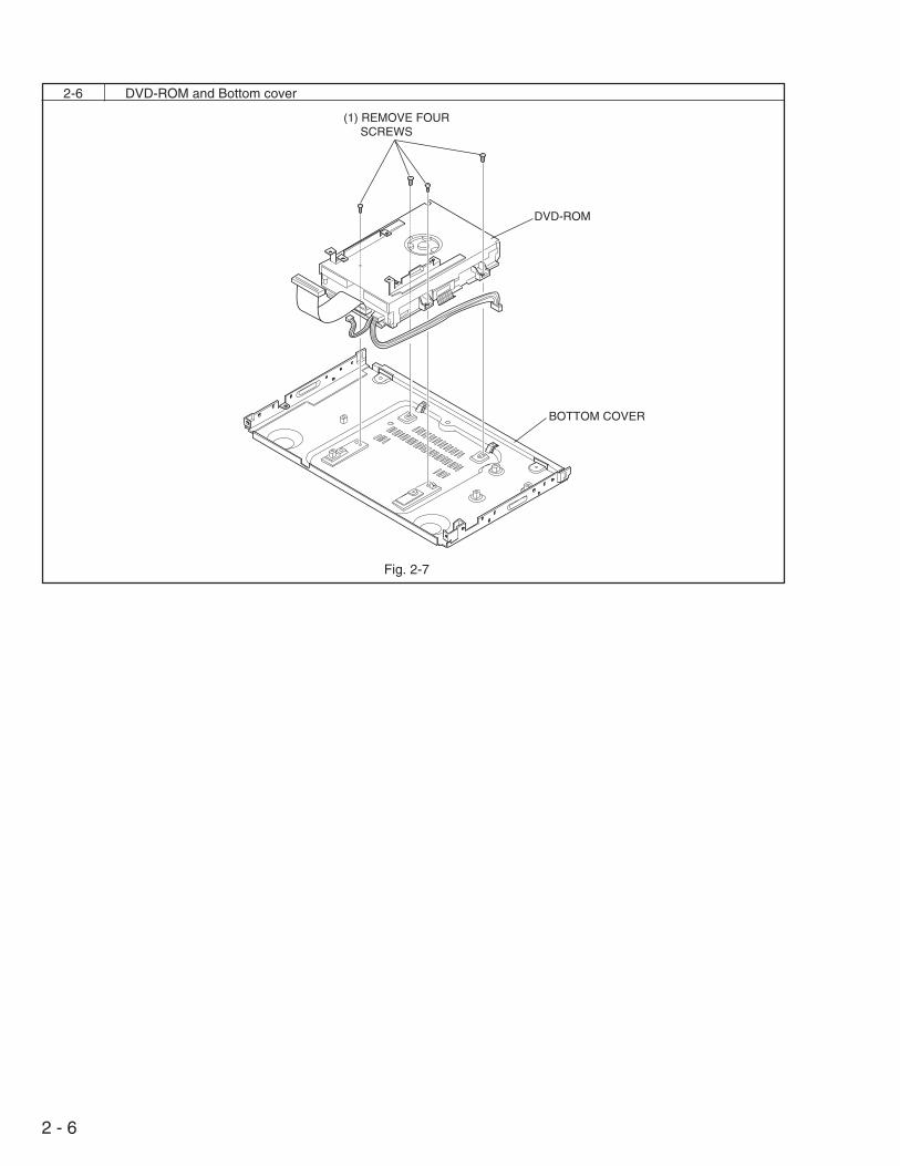
2-6 DVD-ROM and Bottom cover
Fig. 2-7
DVD-ROM
(1) REMOVE FOUR SCREWS
BOTTOM COVER
3 - 1
1 2 3 4
A
B
C
D
E
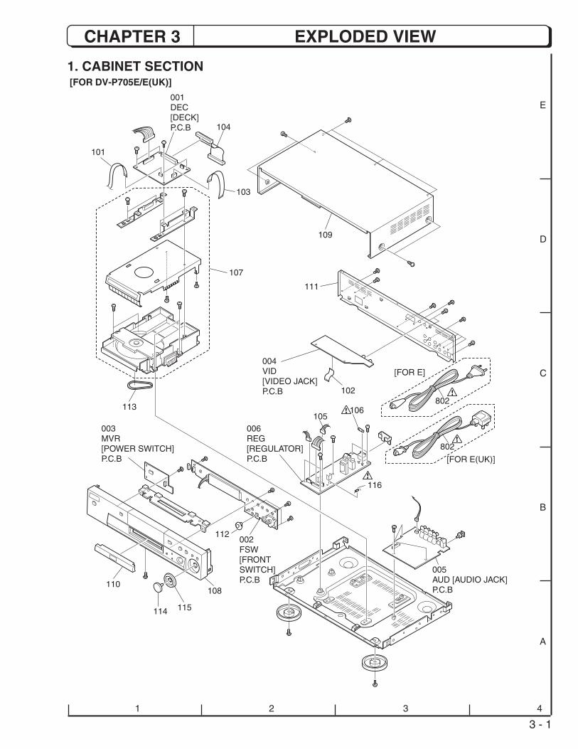
1. CABINET SECTION
CHAPTER 3 EXPLODED VIEW
112
006REG [REGULATOR]P.C.B
005AUD [AUDIO JACK]P.C.B
116
106
108
115114
110
002FSW[FRONT SWITCH]P.C.B
003MVR[POWER SWITCH]P.C.B
113
004VID[VIDEO JACK]P.C.B 102
107
111
109
104
001DEC[DECK]P.C.B
103
105
802
[FOR E]
[FOR E(UK)]
802
101
[FOR DV-P705E/E(UK)]
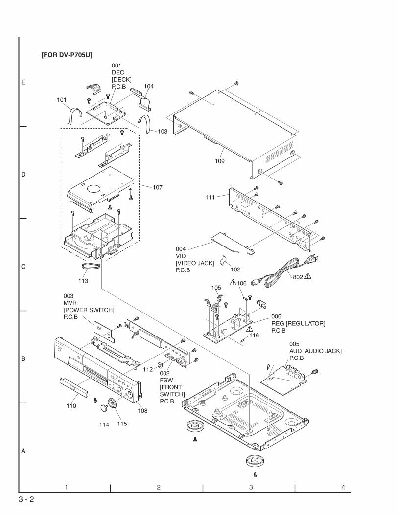
3 - 2
1 2 3 4
A
B
C
D
E
112
006REG [REGULATOR]P.C.B
005AUD [AUDIO JACK]P.C.B
116
106
108
115114
110
002FSW[FRONT SWITCH]P.C.B
003MVR[POWER SWITCH]P.C.B
113
004VID[VIDEO JACK]P.C.B 102
107
111
109
104
001DEC[DECK]P.C.B
103
105
802
101
[FOR DV-P705U]
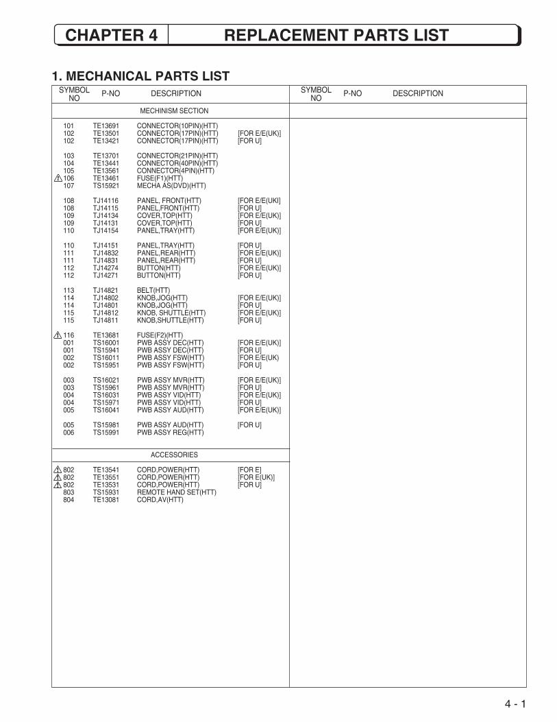
4 - 1
P-NO DESCRIPTIONSYMBOLNO
P-NO DESCRIPTIONSYMBOLNO
1. MECHANICAL PARTS LIST
CHAPTER 4
MECHINISM SECTION
101 TE13691 CONNECTOR(10PIN)(HTT)102 TE13501 CONNECTOR(17PIN)(HTT) [FOR E/E(UK)]102 TE13421 CONNECTOR(17PIN)(HTT) [FOR U]
103 TE13701 CONNECTOR(21PIN)(HTT)104 TE13441 CONNECTOR(40PIN)(HTT)105 TE13561 CONNECTOR(4PIN)(HTT)106 TE13461 FUSE(F1)(HTT)107 TS15921 MECHA AS(DVD)(HTT)
108 TJ14116 PANEL, FRONT(HTT) [FOR E/E(UKI]108 TJ14115 PANEL,FRONT(HTT) [FOR U]109 TJ14134 COVER,TOP(HTT) [FOR E/E(UK)]109 TJ14131 COVER,TOP(HTT) [FOR U]110 TJ14154 PANEL,TRAY(HTT) [FOR E/E(UK)]
110 TJ14151 PANEL,TRAY(HTT) [FOR U]111 TJ14832 PANEL,REAR(HTT) [FOR E/E(UK)]111 TJ14831 PANEL,REAR(HTT) [FOR U]112 TJ14274 BUTTON(HTT) [FOR E/E(UK)]112 TJ14271 BUTTON(HTT) [FOR U]
113 TJ14821 BELT(HTT)114 TJ14802 KNOB,JOG(HTT) [FOR E/E(UK)]114 TJ14801 KNOB,JOG(HTT) [FOR U]115 TJ14812 KNOB, SHUTTLE(HTT) [FOR E/E(UK)]115 TJ14811 KNOB,SHUTTLE(HTT) [FOR U]
116 TE13681 FUSE(F2)(HTT)001 TS16001 PWB ASSY DEC(HTT) [FOR E/E(UK)]001 TS15941 PWB ASSY DEC(HTT) [FOR U]002 TS16011 PWB ASSY FSW(HTT) [FOR E/E(UK)002 TS15951 PWB ASSY FSW(HTT) [FOR U]
003 TS16021 PWB ASSY MVR(HTT) [FOR E/E(UK)]003 TS15961 PWB ASSY MVR(HTT) [FOR U]004 TS16031 PWB ASSY VID(HTT) [FOR E/E(UK)]004 TS15971 PWB ASSY VID(HTT) [FOR U]005 TS16041 PWB ASSY AUD(HTT) [FOR E/E(UK)]
005 TS15981 PWB ASSY AUD(HTT) [FOR U]006 TS15991 PWB ASSY REG(HTT)
ACCESSORIES
802 TE13541 CORD,POWER(HTT) [FOR E]802 TE13551 CORD,POWER(HTT) [FOR E(UK)]802 TE13531 CORD,POWER(HTT) [FOR U]803 TS15931 REMOTE HAND SET(HTT)804 TE13081 CORD,AV(HTT)
REPLACEMENT PARTS LIST

4 - 2
MEMO
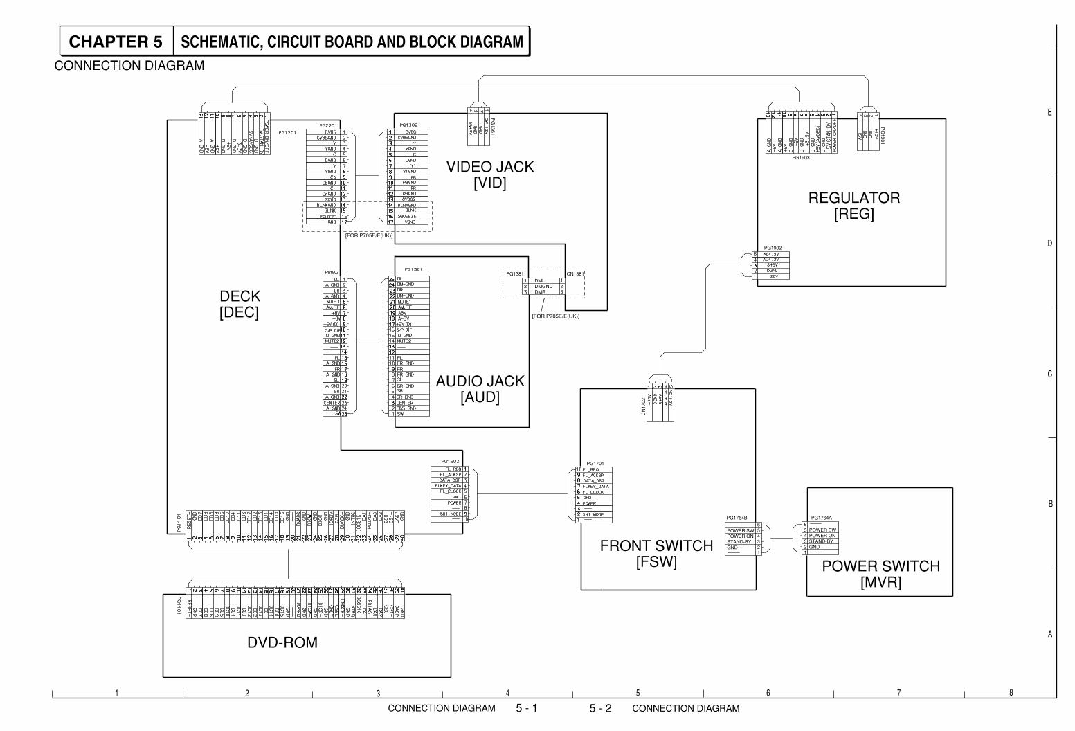
5 - 25 - 1 CONNECTION DIAGRAMCONNECTION DIAGRAM
CONNECTION DIAGRAM
A
B
C
321
D
E
4 65 7 8
CHAPTER 5 SCHEMATIC, CIRCUIT BOARD AND BLOCK DIAGRAM
DECK[DEC]
VIDEO JACK[VID]
AUDIO JACK[AUD]
REGULATOR[REG]
POWER SWITCH[MVR]
DVD-ROM
FRONT SWITCH[FSW]
PG
1361
PG1381 CN1381DMLDMGNDDMR
654321
654321
POWER SWPOWER ONSTAND-BYGND
POWER SWPOWER ONSTAND-BYGND
PG1764B PG1764A
[FOR P705E/E(UK)]
[FOR P705E/E(UK)]
CN
1702
PG1701
PG1903
PG1902
PG
1901
A
B
C
321
D
E
4 65 7 8
5 - 45 - 3 FRONT SWITCHFRONT SWITCH
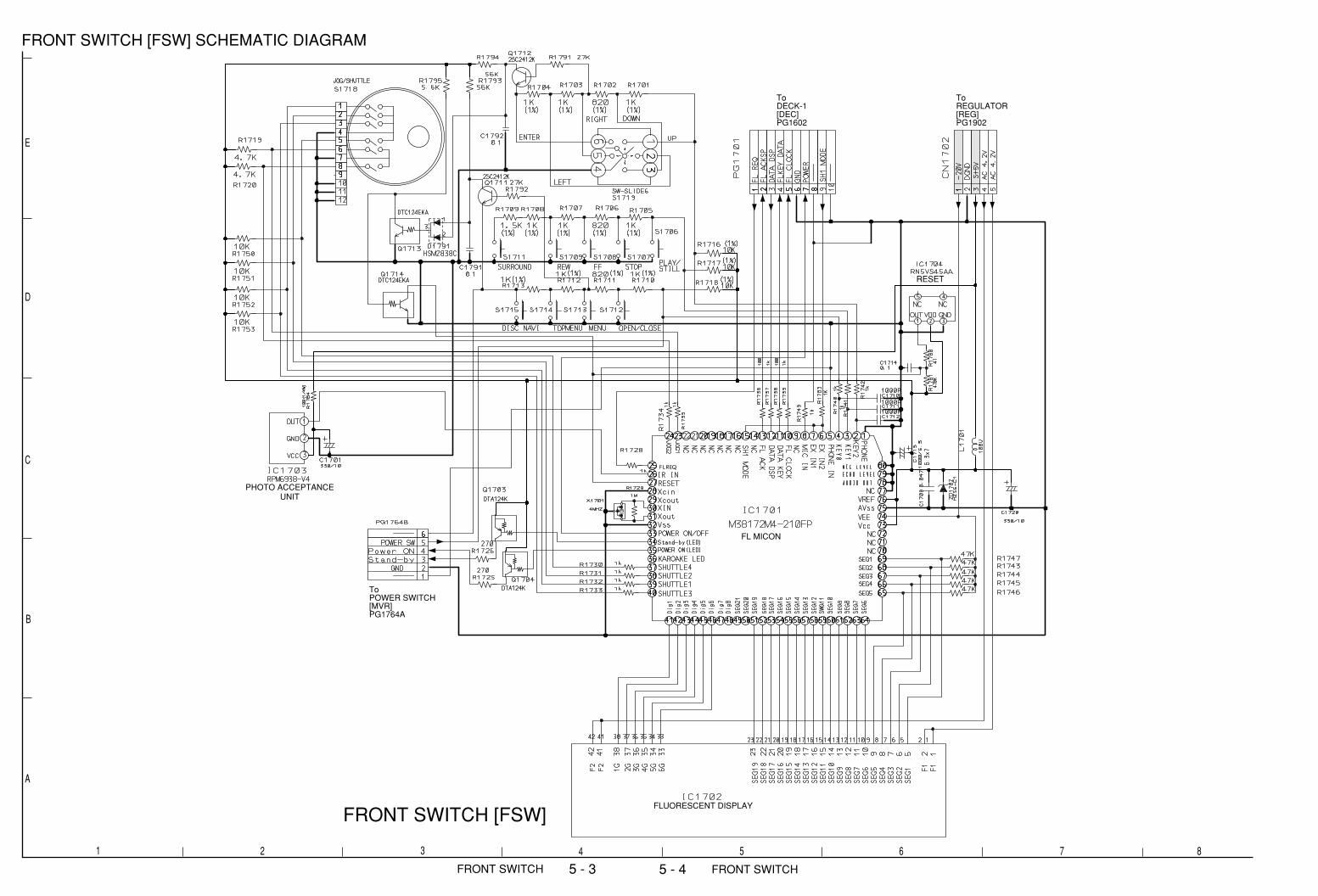
FRONT SWITCH [FSW] SCHEMATIC DIAGRAM
FLUORESCENT DISPLAY
PHOTO ACCEPTANCEUNIT
FL MICON
RESET
ToPOWER SWITCH[MVR]PG1764A
ToDECK-1[DEC]PG1602
ToREGULATOR[REG]PG1902
FRONT SWITCH [FSW]
5 - 65 - 5 VIDEO JACKPOWER SWITCH,VIDEO JACK
POWER SWITCH [MVR] SCHEMATIC DIAGRAM VIDEO JACK [VID] SCHEMATIC DIAGRAM
A
B
C
321
D
E
4 65 7 8
POWER SWITCH [MVR]ToFRONT SWITCH[FSW]PG1764B
MA
3020
DT
C12
4K
[FOR P705U]
[FOR P705E/E(UK)]
ToDECK-1[DEC]PG2201
[FOR P705E/E(UK)]
[FOR P705E/E(UK)]
ToAUDIO JACK[AUD]PG1381
ToREGULATOR[REG]PG1901
VIDEO JACK [VID]
6DB
AM
P
6DB
AM
P
A
B
C
321
D
E
4 65 7 8
5 - 85 - 7 AUDIO JACKAUDIO JACK
AUDIO JACK [AUD] SCHEMATIC DIAGRAM
820p
820p
820p
820p
[FOR P705E/E(UK)]
[FOR P705E/E(UK)]
[FOR P705E/E(UK)]
ToVIDEO JACK[VID]CN1381
AUDIO JACK [AUD]
ToDECK-2[DEC]PG1502
FILTER
FILTER
FILTER
AMP
AMP
AM
P
FILTERAMP
L1301
BUFFER
OPTCAL TRANSMITTER
5 - 105 - 9 REGULATORREGULATOR
REGULATOR [REG] SCHEMATIC DIAGRAM
A
B
C
321
D
E
4 65 7 8
TH1
R2
C3
C2
L1
C1
L N
INLET
D1
D2
C8
R3
R4
C9
D7D5
D6
R6
C10
C11 R9 R8 D9
R11
R10
C6 C7
PHC1
D3
D4
D8
C12
T1
C19
L3
C18
R24
R27
R25
R26C24
VR1
R28
C4
F1
R7
IC1
R5
Q2
C5
R18
D15
R31 R32
D19
D22T2
C26
R30
L4
C27
D21
D20
IC2
C28
L5
D18C25 R33
7
8
R23
D16 C23D17
9
C30
D13 31DF2
C29
D14
C16L2
C17
R12
C14Q3
R13
R14
Q4
R15 R16
R17
Q7
C15D12
C22C21C20R20 R22
R19
R21
R34
R35
Q8
C36
D23
10
11
12
2
4
5
6
R36
D24
D25
C37
6
7
4
5
D203
2
1
8
10
8
13 A GND
12 EV -8
11 A GND
10 EV +8
9 D GND
8 SW +5
7 D GND
6 SW+3.3
5 D GND
4 SW +5
3 D GND
2 EV+4.5
1 P-CON
5
1
2
3
4
SW+12V
GND
GND
SW +5V
EV AC
4 EV AC
3 EV1 +5
2 GND
1 EV-20
C35
C32
C33
C34
PG1903
PG1901
PG1902
IC3
C40
F2
C38 C39
C31
1k
RL1N4005
100/400
RL1N4005
RL1N4005
RL1N4005
15k(1/2W)
15k(1/2W)
470(1/2W)
680k(1/2W)
100k
82k
22k
NTZJ33B
NTZJ24B
1000p
1000p
1000p
1000p
1000p
0.1
0.1
T2.5AH/250V
2200p
1SS133
1SS1331.5k
1.5k
3.3k
0.022
0.022
2SC1815
47p1kV
470 MTZJ3.0B
Q1
2SK
2563
PS2561L1-1-V/W
UPC1093J-P
1/50
1k
1k
1k
2.2k
12k
1.8k
47
1500/10
FMB24L
0.01
1H8
D101H3
D11MTZJ20B
1000p
1000p
1000p
47/50
10
1N4750A
15k
47k
47k
47k
47k
4.7k
2SC1815
2SA1015
1k
1k330/25
470/25
4.7uH
4.7uH
1000/10
1SS133
0.001
33k
2.5A/125V
4.7 0
220/101SS270A
BA033J
100/25 100/25
100/35100/25
100/25
NJM78M08FA
100/10 100/10 0.1
0.1
0.1
0.1
0.1
ToDECK-2[DEC]PG1201
ToVIDEO JACK[VID]PG1361
ToFRONT SWITCH[FSW]CN1702
10k
4747
MTZJ4.7BMTZJ20B
3.3
2SA1015
1H3 1H3
330uH
2.2k
R292.2k
0.033
Q5
2SC
1213
AQ
62S
C12
13A
1SS133
1SS133
1SS133
1SS133
56uH
47/35 47/35
REGULATOR [REG]
A
B
C
321
D
E
4 65 7 8
5 - 125 - 11 DECK-1DECK-1
DECK-1 [DEC] SCHEMATIC DIAGRAM
DEC-1 [DEC]
D1504HSM2838C
100/10
[FOR P705E][FOR P705E]
[FOR P705E]
24A
8A
5A
2A
17A
29A4A
12A13A
28A
25A
27A
23A
6A
9A10A11A
7A
30A
18A
26A
19A
21A
15A
20A
14A
22A
1A
3A
16A
ToDECK-11A-30A
IC1508HD74HC00FP
AUDIO MUTE CONTROL
ToAUDIO JACK[AUD]PG1301
IC501PCM1716E
AUDIO D/A CONVERTER
IC1506PQ20WZ51
AUDIO 5V REGLATOR
AUDIO D/A CONVERTER
IC1505HD74HC04FP
BUFFER
A
B
C
321
D
E
F
G
4 65 7
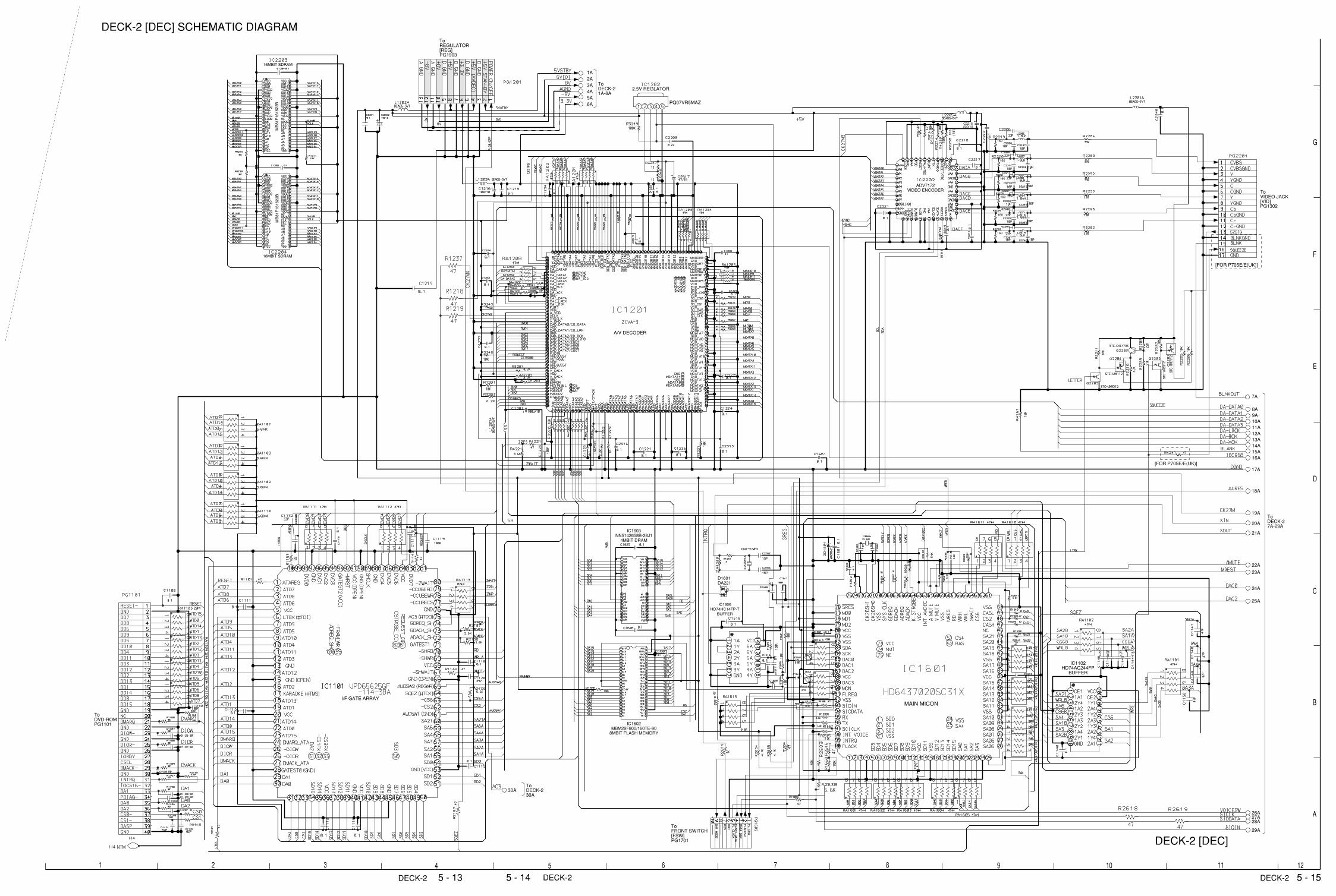
5 - 145 - 13 DECK-2DECK-2
DECK-2 [DEC] SCHEMATIC DIAGRAM
9 10 11 128
5 - 15DECK-2
MB
81F
1616
22B
MB
81F
1616
22B
ToREGULATOR[REG]PG1903
ToDVD-ROMPG1101
PQ07VR5MAZ
D1601DA221
C2215220/10
160
160
160
160
160
160
910
ADV7172VIDEO ENCODER
1A2A3A4A5A6A
ToDECK-21A-6A
ToDECK-27A-29A
[FOR P705E/E(UK)]
ToVIDEO JACK[VID]PG1302
[FOR P705E/E(UK)]
7A
17A
18A
19A
20A
21A
22A
23A
24A
25A
26A27A28A
29A
8A9A10A11A12A13A14A15A16A
ToDECK-230A
30A
ToFRONT SWITCH[FSW]PG1701 DECK-2 [DEC]
16MBIT SDRAM
16MBIT SDRAM
A/V DECODER
I/F GATE ARRAY
2.5V REGLATOR
IC1603NN5142658B-28J1
4MBIT DRAM
IC1602MBM29F800/160TE-90
8MBIT FLASH MEMORY
IC1606HD74HC14FP-T
BUFFER
IC1102HD74AC244FP
BUFFER
MAIN MICON
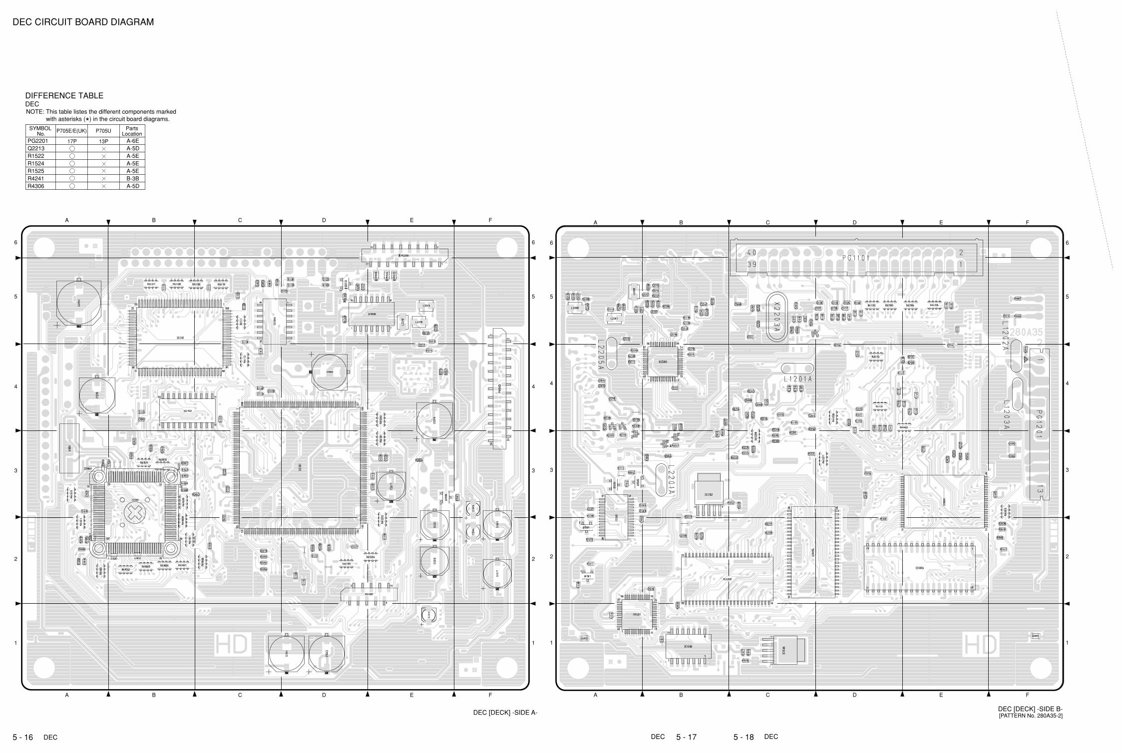
DEC CIRCUIT BOARD DIAGRAM
5 - 185 - 17 DEC5 - 16 DEC DEC
1
2
3
4
5
6
1
2
3
4
5
6
A B C D E F
A B C D E F
DEC [DECK] -SIDE A- DEC [DECK] -SIDE B-[PATTERN No. 280A35-2]
BA
1
2
3
4
5
6
1
2
3
4
5
6
C D E F
BA C D E F
PG2201Q2213R1522R1524R1525R4241R4306
A-6EA-5DA-5EA-5EA-5EB-3BA-5D
DECDIFFERENCE TABLE
SYMBOL No.
PartsLocation
NOTE: This table listes the different components markedwith asterisks (*) in the circuit board diagrams.
17P 13P
P705E/E(UK) P705U
SymbolNo.
PartsLocation
SymbolNo.
PartsLocation
SymbolNo.
PartsLocation
SymbolNo.
PartsLocation
SymbolNo.
PartsLocation
SymbolNo.
PartsLocation
SymbolNo.
PartsLocation
5 - 205 - 19DEC
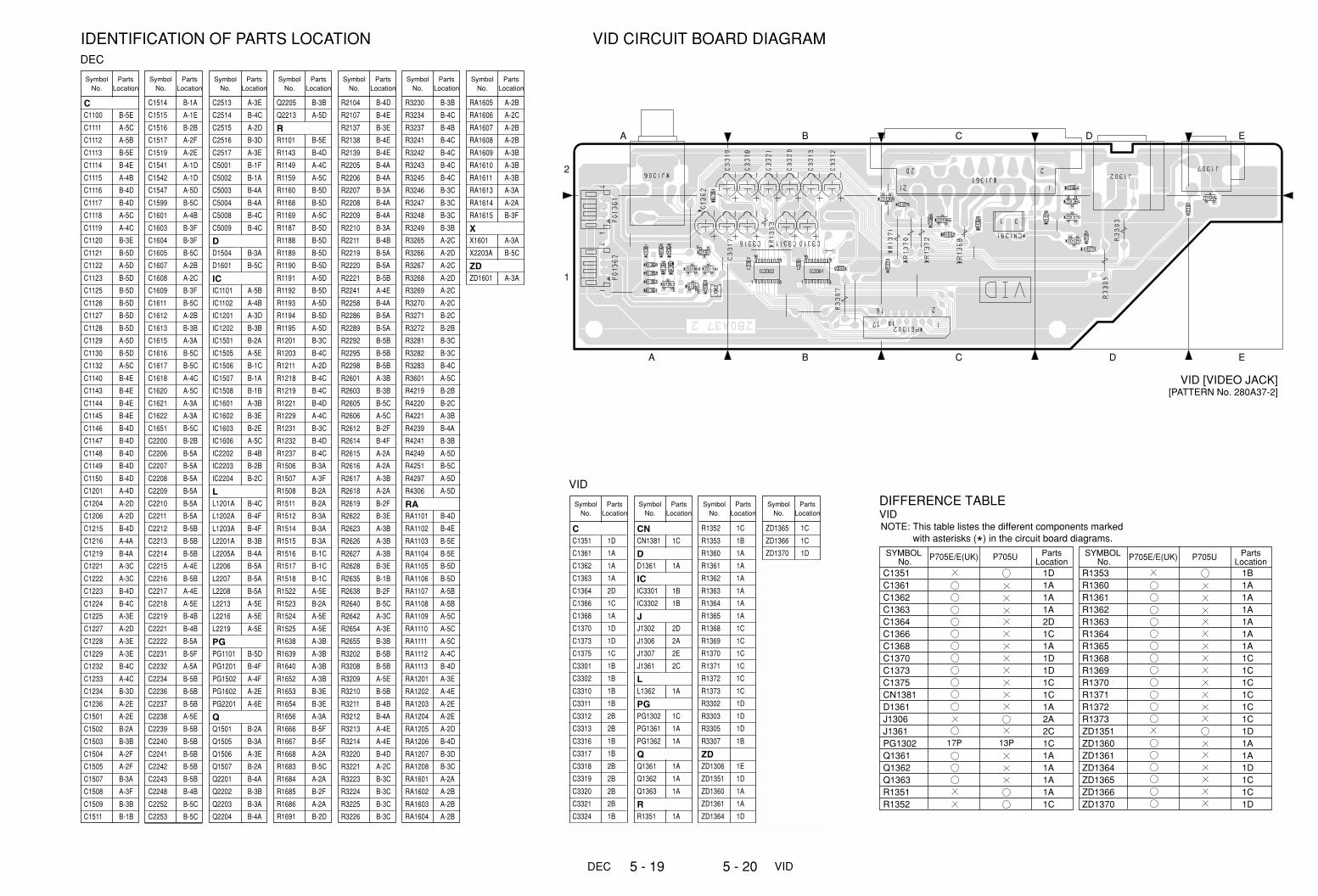
IDENTIFICATION OF PARTS LOCATION VID CIRCUIT BOARD DIAGRAMDEC
VID
13
VID [VIDEO JACK][PATTERN No. 280A37-2]
A B C D E
A
1
2
B C D E
CC1100 B-5E
C1111 A-5C
C1112 A-5B
C1113 B-5E
C1114 B-4E
C1115 A-4B
C1116 B-4D
C1117 B-4D
C1118 A-5C
C1119 A-4C
C1120 B-3E
C1121 B-5D
C1122 A-5D
C1123 B-5D
C1125 B-5D
C1126 B-5D
C1127 B-5D
C1128 B-5D
C1129 A-5D
C1130 B-5D
C1132 A-5C
C1140 B-4E
C1143 B-4E
C1144 B-4E
C1145 B-4E
C1146 B-4D
C1147 B-4D
C1148 B-4D
C1149 B-4D
C1150 B-4D
C1201 A-4D
C1204 A-2D
C1206 A-2D
C1215 B-4D
C1216 A-4A
C1219 B-4A
C1221 A-3C
C1222 A-3C
C1223 B-4D
C1224 B-4C
C1225 A-3E
C1227 A-2D
C1228 A-3E
C1229 A-3E
C1232 B-4C
C1233 A-4C
C1234 B-3D
C1236 A-2E
C1501 A-2E
C1502 B-2A
C1503 B-3B
C1504 A-2F
C1505 A-2F
C1507 B-3A
C1508 A-3F
C1509 B-3B
C1511 B-1B
C1514 B-1A
C1515 A-1E
C1516 B-2B
C1517 A-2F
C1519 A-2E
C1541 A-1D
C1542 A-1D
C1547 A-5D
C1599 B-5C
C1601 A-4B
C1603 B-3F
C1604 B-3F
C1605 B-5C
C1607 A-2B
C1608 A-2C
C1609 B-3F
C1611 B-5C
C1612 A-2B
C1613 B-3B
C1615 A-3A
C1616 B-5C
C1617 B-5C
C1618 A-4C
C1620 A-5C
C1621 A-3A
C1622 A-3A
C1651 B-5C
C2200 B-2B
C2206 B-5A
C2207 B-5A
C2208 B-5A
C2209 B-5A
C2210 B-5A
C2211 B-5A
C2212 B-5B
C2213 B-5B
C2214 B-5B
C2215 A-4E
C2216 B-5B
C2217 A-4E
C2218 A-5E
C2219 B-4B
C2221 B-4B
C2222 B-5A
C2231 B-5F
C2232 A-5A
C2234 B-5B
C2236 B-5B
C2237 B-5B
C2238 A-5E
C2239 B-5B
C2240 B-5B
C2241 B-5B
C2242 B-5B
C2243 B-5B
C2248 B-4B
C2252 B-5C
C2253 B-5C
C2513 A-3E
C2514 B-4C
C2515 A-2D
C2516 B-3D
C2517 A-3E
C5001 B-1F
C5002 B-1A
C5003 B-4A
C5004 B-4A
C5008 B-4C
C5009 B-4C
DD1504 B-3A
D1601 B-5C
ICIC1101 A-5B
IC1102 A-4B
IC1201 A-3D
IC1202 B-3B
IC1501 B-2A
IC1505 A-5E
IC1506 B-1C
IC1507 B-1A
IC1508 B-1B
IC1601 A-3B
IC1602 B-3E
IC1603 B-2E
IC1606 A-5C
IC2202 B-4B
IC2203 B-2B
IC2204 B-2C
LL1201A B-4C
L1202A B-4F
L1203A B-4F
L2201A B-3B
L2205A B-4A
L2206 B-5A
L2207 B-5A
L2208 B-5A
L2213 A-5E
L2216 A-5E
L2219 A-5E
PGPG1101 B-5D
PG1201 B-4F
PG1502 A-4F
PG1602 A-2E
PG2201 A-6E
QQ1501 B-2A
Q1505 B-3A
Q1506 A-3E
Q1507 B-2A
Q2201 B-4A
Q2202 B-3B
Q2203 B-3A
Q2204 B-4A
Q2205 B-3B
Q2213 A-5D
RR1101 B-5E
R1143 B-4D
R1149 A-4C
R1159 A-5C
R1160 B-5D
R1168 B-5D
R1169 A-5C
R1187 B-5D
R1188 B-5D
R1189 B-5D
R1190 B-5D
R1191 A-5D
R1192 B-5D
R1193 A-5D
R1194 B-5D
R1195 A-5D
R1201 B-3C
R1203 B-4C
R1211 A-2D
R1218 B-4C
R1219 B-4C
R1221 B-4D
R1229 A-4C
R1231 B-3C
R1232 B-4D
R1237 B-4C
R1506 B-3A
R1507 A-3F
R1508 B-2A
R1511 B-2A
R1512 B-3A
R1514 B-3A
R1515 B-3A
R1516 B-1C
R1517 B-1C
R1518 B-1C
R1522 A-5E
R1523 B-2A
R1524 A-5E
R1525 A-5E
R1638 A-3B
R1639 A-3B
R1640 A-3B
R1652 A-3B
R1653 B-3E
R1654 B-3E
R1656 A-3A
R1666 B-5F
R1667 B-5F
R1668 A-2A
R1683 B-5C
R1684 A-2A
R1685 B-2F
R1686 A-2A
R1691 B-2D
R2104 B-4D
R2107 B-4E
R2137 B-3E
R2138 B-4E
R2139 B-4E
R2205 B-4A
R2206 B-4A
R2207 B-3A
R2208 B-4A
R2209 B-4A
R2210 B-3A
R2211 B-4B
R2219 B-5A
R2220 B-5A
R2221 B-5B
R2241 A-4E
R2258 B-4A
R2286 B-5A
R2289 B-5A
R2292 B-5B
R2295 B-5B
R2298 B-5B
R2601 A-3B
R2603 B-3B
R2605 B-5C
R2606 A-5C
R2612 B-2F
R2614 B-4F
R2615 A-2A
R2616 A-2A
R2617 A-3B
R2618 A-2A
R2619 B-2F
R2622 B-3E
R2623 A-3B
R2626 A-3B
R2627 A-3B
R2628 B-3E
R2635 B-1B
R2638 B-2F
R2640 B-5C
R2642 A-3C
R2654 A-3E
R2655 B-3B
R3202 B-5B
R3208 B-5B
R3209 A-5E
R3210 B-5B
R3211 B-4B
R3212 B-4A
R3213 A-4E
R3214 A-4E
R3220 B-4D
R3221 A-2C
R3223 B-3C
R3224 B-3C
R3225 B-3C
R3226 B-3C
R3230 B-3B
R3234 B-4C
R3237 B-4B
R3241 B-4C
R3242 B-4C
R3243 B-4C
R3245 B-4C
R3246 B-3C
R3247 B-3C
R3248 B-3C
R3249 B-3B
R3265 A-2C
R3266 A-2D
R3267 A-2C
R3268 A-2D
R3269 A-2C
R3270 A-2C
R3271 B-2C
R3272 B-2B
R3281 B-3C
R3282 B-3C
R3283 B-4C
R3601 A-5C
R4219 B-2B
R4220 B-2C
R4221 A-3B
R4239 B-4A
R4241 B-3B
R4249 A-5D
R4251 B-5C
R4297 A-5D
R4306 A-5D
RARA1101 B-4D
RA1102 B-4E
RA1103 B-5E
RA1104 B-5E
RA1105 B-5D
RA1106 B-5D
RA1107 A-5B
RA1108 A-5B
RA1109 A-5C
RA1110 A-5C
RA1111 A-5C
RA1112 A-4C
RA1113 B-4D
RA1201 A-3E
RA1202 A-4E
RA1203 A-2E
RA1204 A-2E
RA1205 A-2D
RA1206 B-4D
RA1207 B-3D
RA1208 B-3C
RA1601 A-2A
RA1602 A-2B
RA1603 A-2B
RA1604 A-2B
RA1605 A-2B
RA1606 A-2C
RA1607 A-2B
RA1608 A-2B
RA1609 A-3B
RA1610 A-3B
RA1611 A-3B
RA1613 A-3A
RA1614 A-2A
RA1615 B-3F
XX1601 A-3A
X2203A B-5C
ZDZD1601 A-3A
C1351C1361C1362C1363C1364C1366C1368C1370C1373C1375CN1381D1361J1306J1361PG1302Q1361Q1362Q1363R1351R1352
1D1A1A1A2D1C1A1D1D1C1C1A2A2C1C1A1A1A1A1C
VIDDIFFERENCE TABLE
SYMBOL No.
PartsLocation
NOTE: This table listes the different components markedwith asterisks (*) in the circuit board diagrams.
R1353R1360R1361R1362R1363R1364R1365R1368R1369R1370R1371R1372R1373ZD1351ZD1360ZD1361ZD1364ZD1365ZD1366ZD1370
1B1A1A1A1A1A1A1C1C1C1C1C1C1D1A1A1D1C1C1D
SYMBOL No.
PartsLocation
13P17P
P705E/E(UK) P705U P705E/E(UK) P705U
SymbolNo.
PartsLocation
SymbolNo.
PartsLocation
SymbolNo.
PartsLocation
SymbolNo.
PartsLocation
CC1351 1D
C1361 1A
C1362 1A
C1363 1A
C1364 2D
C1366 1C
C1368 1A
C1370 1D
C1373 1D
C1375 1C
C3301 1B
C3302 1B
C3310 1B
C3311 1B
C3312 2B
C3313 2B
C3316 1B
C3317 1B
C3318 2B
C3319 2B
C3320 2B
C3321 2B
C3324 1B
CNCN1381 1C
DD1361 1A
ICIC3301 1B
IC3302 1B
JJ1302 2D
J1306 2A
J1307 2E
J1361 2C
LL1362 1A
PGPG1302 1C
PG1361 1A
PG1362 1A
QQ1361 1A
Q1362 1A
Q1363 1A
RR1351 1A
R1352 1C
R1353 1B
R1360 1A
R1361 1A
R1362 1A
R1363 1A
R1364 1A
R1365 1A
R1368 1C
R1369 1C
R1370 1C
R1371 1C
R1372 1C
R1373 1C
R3302 1D
R3303 1D
R3305 1D
R3307 1B
ZDZD1306 1E
ZD1351 1D
ZD1360 1A
ZD1361 1A
ZD1364 1D
ZD1365 1C
ZD1366 1C
ZD1370 1D
VID
5 - 225 - 21 AUDAUD
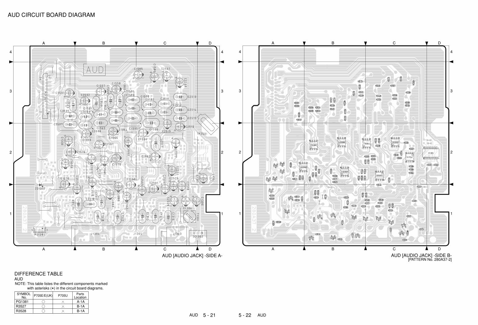
AUD CIRCUIT BOARD DIAGRAM
AUD [AUDIO JACK] -SIDE A-
BA
1
2
3
4
1
2
3
4
C D
BA C D
AUD [AUDIO JACK] -SIDE B-[PATTERN No. 280A37-2]
BA
1
2
3
4
1
2
3
4
C D
BA C D
PG1381R3527R3528
A-1AB-1AB-1A
AUDDIFFERENCE TABLE
SYMBOL No.
PartsLocationP705E/E(UK) P705U
NOTE: This table listes the different components markedwith asterisks (*) in the circuit board diagrams.
SymbolNo.
PartsLocation
SymbolNo.
PartsLocation
SymbolNo.
PartsLocation
SymbolNo.
PartsLocation
SymbolNo.
PartsLocation
SymbolNo.
PartsLocation
SymbolNo.
PartsLocation
5 - 24 REG5 - 23AUD,REG
IDENTIFICATION OF PARTS LOCATION REG CIRCUIT BOARD DIAGRAMAUD REG
CN1
C1
L1
TH1
F1
D6
D5
R4
R3
C8C2
D1
D2Q1
Q2
R7
C10
D7
C9
R10
D9
D25D8
R8
C12D3
R2
C6C3 C4
C7
C5
PHC1
T1
R23
R24R26
IC1
R18R12
C29
D10
C14
D13
D14
D24D15 C24
VR1D16
D17
C30
C16 C18
C23
D11
Q3
FG3
Q5 Q6
R30C26
R29
T2
L2
L3
C17 C19Q4
D23 C38
R22
IC3 Q8
L4
D18
F2 R34 D19D20
D22
D21
R31
R32 C27R36
D12 C20 C39 C21
IC2
PG1901
1 3
13
1 3 5 7 9 11 13
5
4 C22
C15C25
C28
PG1902FG1
FG2PG1903
REG[REGULATOR][PATTERN No. 257A27-2]
12 11 9 7
2 4 5 6
C
B
C
C
C
C
E
E
E
E B
B
B
B
1 3 5
10 8 6
C
E
B
E
R17
R13
Q7R20
R15
R16
R21R19
C40
1
2
3
4
1
2
3
4
A B
A B
CC1301 A-2D
C1302 B-2D
C1303 B-1C
C1304 A-1C
C1305 B-2D
C1306 A-1C
C1307 B-1C
C1312 A-1B
C1313 A-1C
C1314 A-1C
C1316 A-1C
C1317 A-1B
C1318 A-1B
C1319 B-1C
C1320 B-1C
C1322 B-1B
C1325 B-1B
C1330 A-2A
C1333 A-2B
C1338 B-1C
C1374 B-1C
C1557 A-3B
C1558 A-3B
C1559 A-3B
C1560 A-3B
C1561 A-3B
C1562 A-3B
C1563 A-2B
C1564 A-3B
C1565 A-2B
C1566 A-2B
C1567 A-2B
C1568 A-2B
C1571 B-2B
C1572 B-2B
C1575 A-2A
C1576 A-2A
C1579 A-2B
C1580 A-1B
C1583 A-1B
C1584 A-1B
C1585 A-3C
C1586 A-3C
C1589 A-3B
C1590 A-3C
C1591 A-3B
C1592 A-3C
C1593 A-2B
C1594 A-2C
C1595 A-3B
C1596 A-2C
C1597 B-2C
C1598 B-2C
C2501 A-1C
C2502 A-2C
C2505 A-1C
C2506 A-1C
C2507 A-3C
C2508 A-3C
C2510 A-3C
C2511 A-3C
C2512 A-3C
C2513 A-3C
C2514 A-3C
C2515 A-2C
C2516 A-2C
C2517 A-2C
C2518 A-1C
C2519 B-2C
C2521 A-2C
C2522 A-2C
C2525 A-1C
C2526 A-1C
C3501 A-3A
C3502 A-3B
C3503 A-3A
C3504 A-3B
C3505 A-3A
C3506 A-3B
C3507 A-2A
C3508 A-2B
C3509 A-2A
C3510 A-2B
C3511 B-2A
C3512 B-2B
C3515 A-1B
C3516 A-2B
C3517 A-1B
C3518 A-1B
C3519 B-1B
DD1302 B-2A
D1303 B-2A
D1304 B-2A
D1504 B-1A
D1505 B-2A
D3301 B-2A
ICIC1301 B-2D
IC1302 A-1D
IC1507 B-2B
IC1508 B-2B
IC1509 B-2A
IC1510 B-2B
IC1511 B-2C
IC1512 B-2C
IC1513 B-2C
IC1514 B-2C
JJ1303 A-1C
J1304 A-1B
J1305 A-1B
LL1301 A-2D
PG
PG1301 A-3A
PG1381 A-1A
QQ1306 B-1B
Q1307 B-1C
Q1308 B-1C
Q1309 B-1C
Q1310 B-1B
Q1311 B-1B
Q3503 B-1A
Q3504 B-1A
RR1307 B-1C
R1314 B-1B
R1315 B-1B
R1316 B-1B
R1317 B-1C
R1318 B-1B
R1319 B-1B
R1320 B-1C
R1321 B-1C
R1322 B-1C
R1323 B-1C
R1527 B-3B
R1528 B-3B
R1529 B-3B
R1530 B-3B
R1531 B-3B
R1532 B-3B
R1533 A-2B
R1534 B-2B
R1539 B-2B
R1540 B-2B
R1543 B-2B
R1544 B-2B
R1545 B-3B
R1546 B-3C
R1547 B-3B
R1548 B-3C
R1549 B-3B
R1550 B-3C
R1551 B-2B
R1552 B-2C
R1553 B-2C
R1554 B-1C
R1555 B-2C
R1556 B-2C
R1557 B-3C
R1558 B-3C
R1559 B-3C
R1560 B-3C
R1561 B-3C
R1562 B-3C
R1563 B-2C
R1564 B-2C
R1565 B-2C
R1566 B-2C
R1567 B-2C
R1568 B-2C
R1569 B-3C
R1570 B-3C
R1571 B-3C
R1572 B-3B
R1573 B-3B
R1574 B-3B
R1579 B-1B
R1580 B-1B
R1581 B-2C
R1582 B-2C
R1583 B-2C
R2450 B-1A
R2523 B-1B
R2524 B-1B
R2530 B-1A
R2531 B-1C
R2532 B-1C
R2533 B-1C
R2534 B-1C
R3501 B-3A
R3502 B-3B
R3503 B-3A
R3504 B-3B
R3505 B-3A
R3506 B-3B
R3507 B-3A
R3508 B-3B
R3509 B-2A
R3510 B-2B
R3511 B-2A
R3512 B-2B
R3513 B-2A
R3514 B-2B
R3515 B-1A
R3516 B-1B
R3517 B-1A
R3518 B-1B
R3519 B-1A
R3520 B-1B
R3523 B-2A
R3524 B-2B
R3525 B-2B
R3526 B-2B
R3527 B-1A
R3528 B-1A
TT1301 A-1C
TPTP2501 A-2D
ZDZD1301 B-1C
ZD1303 B-1B
ZD1304 B-1B
ZD1305 B-1C
ZD1307 A-1A
ZD3501 B-1B
CC0001 4B
C0002 4B
C0003 3B
C0004 3B
C0005 3B
C0006 3A
C0007 3B
C0008 4A
C0009 3A
C0010 3A
C0012 3A
C0014 2A
C0015 1A
C0016 2A
C0017 2A
C0018 2A
C0019 2A
C0020 1A
C0021 1A
C0022 1A
C0023 2A
C0024 2B
C0025 1B
C0026 2B
C0027 1B
C0028 1B
C0029 2A
C0030 2A
C0038 1A
C0039 1A
C0040 1A
CNCN0001 4A
DD0001 3B
D0002 3B
D0003 3A
D0005 4A
D0006 4A
D0007 3A
D0008 3A
D0009 3A
D0010 2A
D0011 2A
D0012 1A
D0013 2A
D0014 2A
D0015 2A
D0016 2A
D0017 2A
D0018 1B
D0019 1B
D0020 1B
D0021 1B
D0022 1B
D0023 1A
D0024 2A
D0025 3A
FF0001 4A
F0002 1A
FGFG0001 1A
FG0002 1B
FG0003 2A
ICIC0001 3B
IC0002 1A
IC0003 1A
LL0001 4B
L0002 2A
L0003 2A
L0004 2A
PGPG1901 1A
PG1902 1B
PG1903 1A
PHCPHC0001 3A
QQ0001 3A
Q0002 3A
Q0003 2A
Q0004 2A
Q0005 2B
Q0006 2B
Q0008 1A
RR0002 3B
R0003 4A
R0004 4A
R0007 3A
R0008 3A
R0010 3A
R0012 2A
R0013 2A
R0015 2A
R0016 1A
R0017 2A
R0018 2A
R0019 1A
R0020 1A
R0021 1A
R0022 1A
R0023 2A
R0024 2B
R0026 3B
R0029 2A
R0030 2A
R0031 1B
R0032 1B
R0034 1A
R0036 1A
T
T0001 3A
T0002 2B
THTH0001 4A
VRVR0001 2B
5 - 26 FSW5 - 25FSW,MVR
FSW, MVR CIRCUIT BOARD DIAGRAMS
FSW
FSW [FRONT SWITCH][PATTERN No. 280A37-2]
BA
1
2
C D E F H I
BA C D E F H I
MVR [POWER SWITCH][PATTERN No. 280A37-2]
SymbolNo.
PartsLocation
SymbolNo.
PartsLocation
SymbolNo.
PartsLocation
SymbolNo.
PartsLocation
SymbolNo.
PartsLocation
IDENTIFICATION OF PARTS LOCATION
CC1701 2H
C1708 2C
C1710 2B
C1711 2B
C1712 2C
C1714 2C
C1715 1B
C1720 1B
C1791 2B
C1792 1B
CNCN1702 2I
DD1791 2B
ICIC1701 1C
IC1702 2F
IC1703 2H
IC1704 2C
LL1701 2H
PGPG1701 1B
PG1764 2I
QQ1703 2I
Q1704 2I
Q1711 1C
Q1712 1B
Q1713 2B
Q1714 1B
RR1701 1C
R1702 1B
R1703 1B
R1704 1B
R1705 2B
R1706 2B
R1707 2A
R1708 2A
R1709 2C
R1710 2D
R1711 1C
R1712 1C
R1713 1C
R1716 2A
R1717 2B
R1718 2D
R1719 2A
R1720 2A
R1725 2I
R1726 2I
R1728 1B
R1729 1B
R1730 1B
R1731 1B
R1732 1B
R1733 1B
R1734 1B
R1735 2B
R1736 2B
R1737 2B
R1738 2B
R1739 2A
R1740 2B
R1741 2C
R1742 2C
R1743 2F
R1744 2F
R1745 2F
R1746 2F
R1747 2F
R1749 2A
R1750 2A
R1751 2A
R1752 2A
R1753 2A
R1780 2C
R1781 2C
R1783 2B
R1784 2H
R1791 1B
R1792 1C
R1793 2B
R1794 2B
R1795 2B
SS1706 2B
S1707 2B
S1708 2A
S1709 2A
S1711 2I
S1712 2C
S1713 1C
S1714 1C
S1715 1C
S1718 1A
S1719 1B
XX1701 1B
ZDZD1702 2C

A
B
C
321
D
E
4
5 - 27BLOCK DIAGRAM
BLOCK DIAGRAM
PG1101
ATAPI
DVD-ROM
REQUEST,CSTROBE,
ZWAIT,ZRD,ZWR FRAMWR
DVD[0:7]
IC1601
IC1201
IC1101
X2203
XíTAL27MHz IC1505
IC1602
8MbitFLASH
IC1603
4MbitDRAM
IC1202
X1601
XíTAL20MHz
COMPORNENT OUT
IC1302
OPT OUT
FL/R OUT
DML/R OUT
SVIDEO OUT VIDEO OUT
IC1507
IC3301
IC3302
VID EO DRIVER
DML/R
SCL,SDA
SD[0:15]
DA_BCK
DA_LRCK
H/VSYNC
VDATA[0:7]
MADDR[0:11]
MDATA[0:15]
FL/R,SL/R,
CENTER,SUB
BLANKOUT
DML/R
DA_DATA0
1:3DA_DATA [ ]
SA[0:21]
IC2203
IC2204
16MbitSDRAM
IC1501
IC1507
PG1502
AUDIO CON
MUTE2
MUTE1
IC1508
Q1501
Q1507
IC2201
ADV7172
PG2201
VIDEO CON
DA
C0/2,S
ICLK
,SIO
DA
T
CS2,RD,WR,etc PG1602
FL CON
IC1506
PG
1302 P
G1301
CENTER
SUB
SL/R FL/R
DECK PWB
FRONT PWBPOWER SWITCH PWB
AUDIO JACK PWB
VIDEO JACK PWB
IC1509
IC1508 IC1510
MUTE
MUTE
IC1511
IC1513 IC1512
IC1514 SL/R OUT CENTER OUT
COAXIAT OUT
SUB WOFFER OUT
IC1301BUFFER
IC1701S1761
FL uCOM
IC1702
FL DISPLAY
MAIN MICON
BUFFER
I/F GATE ARRAYA/V DECODER
VIEOENCODER
AUDIO 5VREGULATOR
AUDIO D/ACONVERTER
AUDIO D/ACONVERTER

����������� �����������������������������
DV-P705EDV-P705E(UK)DV-P705U
��������� � �����
Digital Media Products Division, TokaiTK No.9010E
DV
-P70
5E/E
(UK
)/U
DV
-P705E
/E(U
K)/U


![Commas Until You Cry ! Blah blah blah [pause =, ] blah blah blah [pause =, ] blah blah blah... Blah blah blah [pause =, ] blah blah blah [pause =, ]](https://img.pdfslide.us/doc/110x75/56649f295503460f94c42b3e/commas-until-you-cry-blah-blah-blah-pause-blah-blah-blah-pause-.jpg)