Embed Size (px)
Citation preview
978-1-4673-7676-1/16/$31.00 ©2016 IEEE 1
DVB-S2 Software Defined Radio Modem
on the RC64 Manycore DSP
Peleg Aviely, Olga Radovsky and Ran Ginosar
Ramon Chips, Ltd., 5 HaCarmel Street, Yoqneam Illit 2069201, Israel
+972-722 216869
[peleg, olga, ran]@ramon-chips.com
Abstract— This paper describes high performance
implementation of DVB-S2 modem on the rad-hard manycore
RC64 DSP. Multi-level simulation and development
methodologies are described. Modem algorithms are specified,
together with implementation details. Efficient parallel
processing is enabled by the shared memory architecture, by
PRAM-like task oriented programming and by dynamic
allocation of tasks to cores. The modem achieves in excess of 2
Gbps transmission and 1 Gbps reception.
TABLE OF CONTENTS
1. INTRODUCTION ................................................1
2. RC64 DVB-S2 SIMULATOR ............................1
3. RC64 DVB-S2 MODEM ALGORITHMS ...........2
4. MODEM IMPLEMENTATION .............................5
5. PERFORMANCE ................................................9
6. CONCLUSIONS ..................................................9
ACKNOWLEDGEMENT ........................................10
REFERENCES .......................................................10
BIOGRAPHY ........................................................10
1. INTRODUCTION
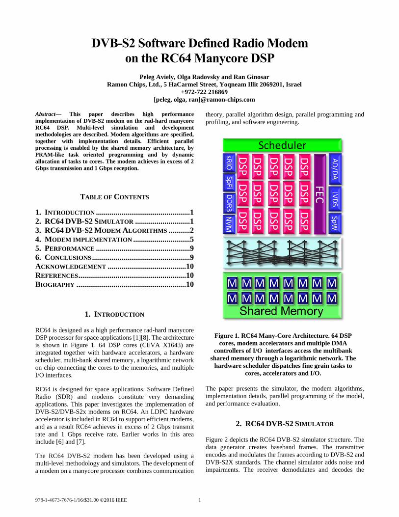
RC64 is designed as a high performance rad-hard manycore
DSP processor for space applications [1][8]. The architecture
is shown in Figure 1. 64 DSP cores (CEVA X1643) are
integrated together with hardware accelerators, a hardware
scheduler, multi-bank shared memory, a logarithmic network
on chip connecting the cores to the memories, and multiple
I/O interfaces.
RC64 is designed for space applications. Software Defined
Radio (SDR) and modems constitute very demanding
applications. This paper investigates the implementation of
DVB-S2/DVB-S2x modems on RC64. An LDPC hardware
accelerator is included in RC64 to support efficient modems,
and as a result RC64 achieves in excess of 2 Gbps transmit
rate and 1 Gbps receive rate. Earlier works in this area
include [6] and [7].
The RC64 DVB-S2 modem has been developed using a
multi-level methodology and simulators. The development of
a modem on a manycore processor combines communication
theory, parallel algorithm design, parallel programming and
profiling, and software engineering.
Figure 1. RC64 Many-Core Architecture. 64 DSP
cores, modem accelerators and multiple DMA
controllers of I/O interfaces access the multibank
shared memory through a logarithmic network. The
hardware scheduler dispatches fine grain tasks to
cores, accelerators and I/O.
The paper presents the simulator, the modem algorithms,
implementation details, parallel programming of the model,
and performance evaluation.
2. RC64 DVB-S2 SIMULATOR
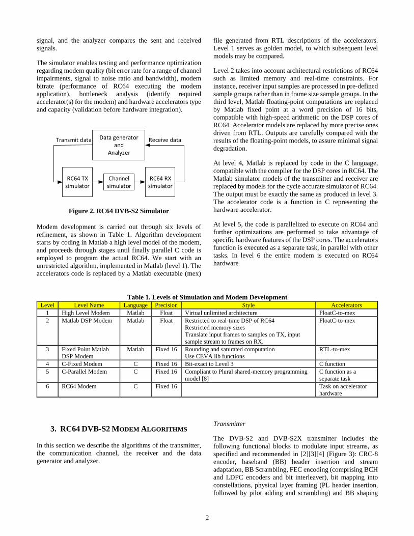
Figure 2 depicts the RC64 DVB-S2 simulator structure. The
data generator creates baseband frames. The transmitter
encodes and modulates the frames according to DVB-S2 and
DVB-S2X standards. The channel simulator adds noise and
impairments. The receiver demodulates and decodes the
2
signal, and the analyzer compares the sent and received
signals.
The simulator enables testing and performance optimization
regarding modem quality (bit error rate for a range of channel
impairments, signal to noise ratio and bandwidth), modem
bitrate (performance of RC64 executing the modem
application), bottleneck analysis (identify required
accelerator(s) for the modem) and hardware accelerators type
and capacity (validation before hardware integration).
RC64 TX simulator
Channel simulator
RC64 RX simulator
Data generatorand
Analyzer
Transmit data Receive data
Figure 2. RC64 DVB-S2 Simulator
Modem development is carried out through six levels of
refinement, as shown in Table 1. Algorithm development
starts by coding in Matlab a high level model of the modem,
and proceeds through stages until finally parallel C code is
employed to program the actual RC64. We start with an
unrestricted algorithm, implemented in Matlab (level 1). The
accelerators code is replaced by a Matlab executable (mex)
file generated from RTL descriptions of the accelerators.
Level 1 serves as golden model, to which subsequent level
models may be compared.
Level 2 takes into account architectural restrictions of RC64
such as limited memory and real-time constraints. For
instance, receiver input samples are processed in pre-defined
sample groups rather than in frame size sample groups. In the
third level, Matlab floating-point computations are replaced
by Matlab fixed point at a word precision of 16 bits,
compatible with high-speed arithmetic on the DSP cores of
RC64. Accelerator models are replaced by more precise ones
driven from RTL. Outputs are carefully compared with the
results of the floating-point models, to assure minimal signal
degradation.
At level 4, Matlab is replaced by code in the C language,
compatible with the compiler for the DSP cores in RC64. The
Matlab simulator models of the transmitter and receiver are
replaced by models for the cycle accurate simulator of RC64.
The output must be exactly the same as produced in level 3.
The accelerator code is a function in C representing the
hardware accelerator.
At level 5, the code is parallelized to execute on RC64 and
further optimizations are performed to take advantage of
specific hardware features of the DSP cores. The accelerators
function is executed as a separate task, in parallel with other
tasks. In level 6 the entire modem is executed on RC64
hardware
Table 1. Levels of Simulation and Modem Development
Level Level Name Language Precision Style Accelerators
1 High Level Modem Matlab Float Virtual unlimited architecture FloatC-to-mex
2 Matlab DSP Modem Matlab Float Restricted to real-time DSP of RC64
Restricted memory sizes
Translate input frames to samples on TX, input
sample stream to frames on RX.
FloatC-to-mex
3 Fixed Point Matlab
DSP Modem
Matlab Fixed 16 Rounding and saturated computation
Use CEVA lib functions
RTL-to-mex
4 C-Fixed Modem C Fixed 16 Bit-exact to Level 3 C function
5 C-Parallel Modem C Fixed 16 Compliant to Plural shared-memory programming
model [8]
C function as a
separate task
6 RC64 Modem C Fixed 16 Task on accelerator
hardware
3. RC64 DVB-S2 MODEM ALGORITHMS
In this section we describe the algorithms of the transmitter,
the communication channel, the receiver and the data
generator and analyzer.
Transmitter
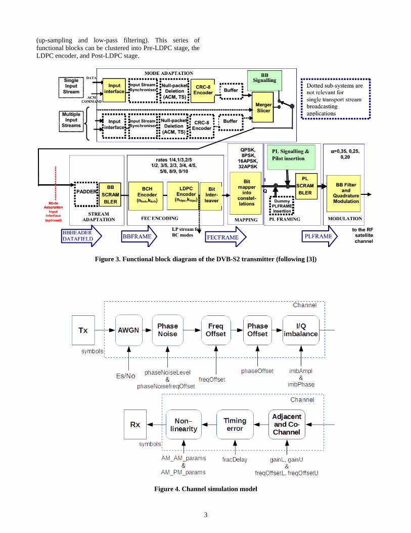
The DVB-S2 and DVB-S2X transmitter includes the
following functional blocks to modulate input streams, as
specified and recommended in [2][3][4] (Figure 3): CRC-8
encoder, baseband (BB) header insertion and stream
adaptation, BB Scrambling, FEC encoding (comprising BCH
and LDPC encoders and bit interleaver), bit mapping into
constellations, physical layer framing (PL header insertion,
followed by pilot adding and scrambling) and BB shaping
3
(up-sampling and low-pass filtering). This series of
functional blocks can be clustered into Pre-LDPC stage, the
LDPC encoder, and Post-LDPC stage.
Figure 3. Functional block diagram of the DVB-S2 transmitter (following [3])
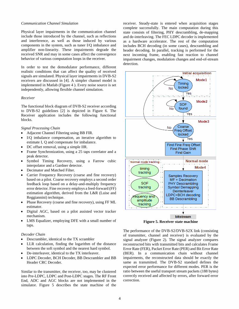
Figure 4. Channel simulation model
4
Communication Channel Simulation
Physical layer impairments in the communication channel
include those introduced by the channel, such as reflections
and interference, as well as those induced by various
components in the system, such as tuner I/Q imbalance and
amplifier non-linearity. These impairments degrade the
received SNR and may in some cases affect the convergence
behavior of various computation loops in the receiver.
In order to test the demodulator performance, different
realistic conditions that can affect the quality of received
signals are simulated. Physical layer impairments in DVB-S2
receivers are discussed in [4]. A simpler channel model is
implemented in Matlab (Figure 4 ). Every noise source is set
independently, allowing flexible channel simulation.
Receiver
The functional block diagram of DVB-S2 receiver according
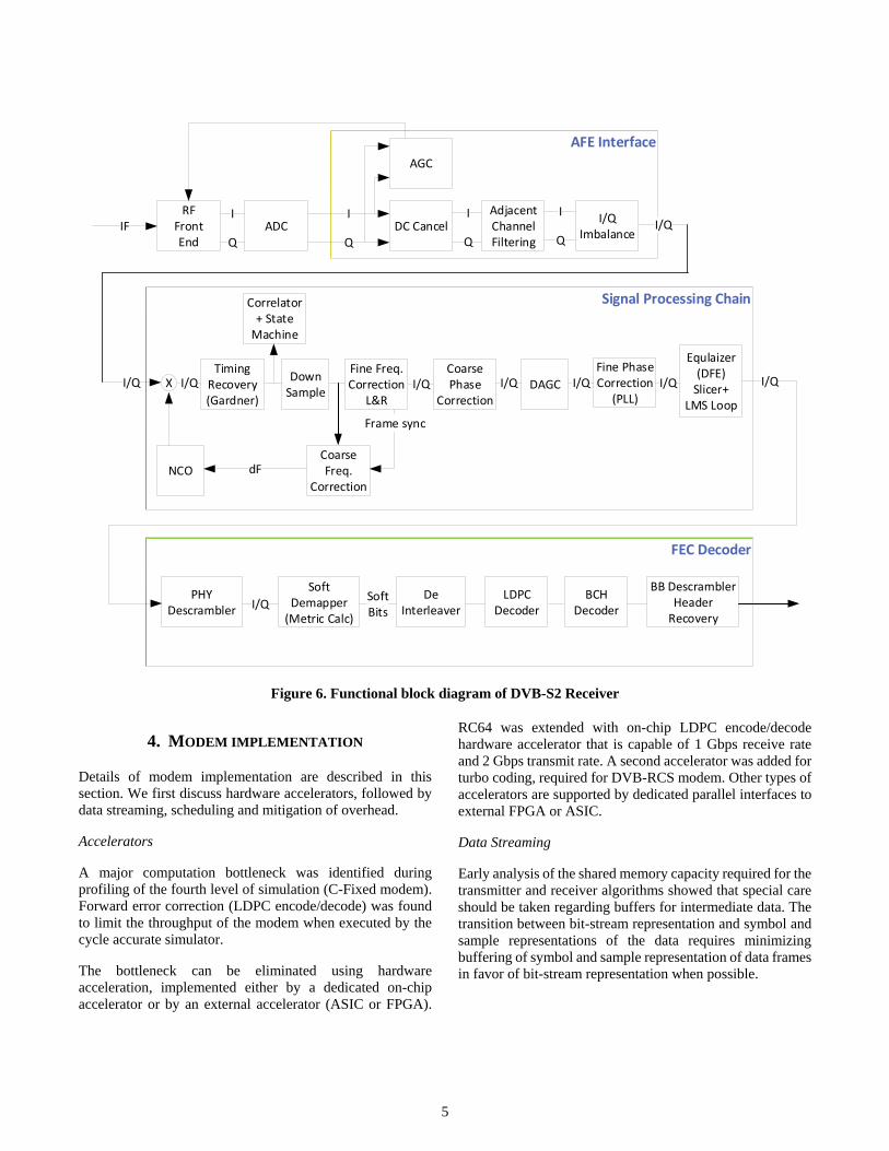
to DVB-S2 guidelines [2] is depicted in Figure 6. The
Receiver application includes the following functional
blocks.
Signal Processing Chain
Adjacent Channel Filtering using BB FIR.
I/Q imbalance compensation, an iterative algorithm to
estimate I, Q and compensate for imbalance.
DC offset removal, using a simple IIR.
Frame Synchronization, using a 25 taps correlator and a
peak detector.
Symbol Timing Recovery, using a Farrow cubic
interpolator and a Gardner detector.
Decimator and Matched Filter.
Carrier Frequency Recovery (coarse and fine recovery)
based on a pilot. Coarse recovery employs a second order
feedback loop based on a delay-and-multiply frequency
error detector. Fine recovery employs a feed-forward (FF)
estimation algorithm, derived from the L&R (Luise and
Reggiannini) technique.
Phase Recovery (coarse and fine recovery), using FF ML
estimator.
Digital AGC, based on a pilot assisted vector tracker
mechanism.
LMS Equalizer, employing DFE with a small number of
taps.
Decoder Chain
Descrambler, identical to the TX scrambler
LLR calculation, finding the logarithm of the distance
between the soft symbol and the nearest hard symbol.
De-interleaver, identical to the TX interleaver.
LDPC Decoder, BCH Decoder, BB Descrambler and BB
Header CRC Decoder.
Similar to the transmitter, the receiver, too, may be clustered
into Pre-LDPC, LDPC and Post-LDPC stages. The RF Front
End, ADC and AGC blocks are not implemented in the
simulator. Figure 5 describes the state machine of the
receiver. Steady-state is entered when acquisition stages
complete successfully. The main computation during this
state consists of filtering, PHY descrambling, de-mapping
and de-interleaving. The FEC LDPC decoder is implemented
as a hardware accelerator. The rest of the computation
includes BCH decoding (in some cases), descrambling and
header decoding. In parallel, tracking is performed for the
next incoming frame, enabling fast reaction to channel
impairment changes, modulation changes and end-of-stream
detection.
Figure 5. Receiver state machine
The performance of the DVB-S2/DVB-S2X link (consisting
of transmitter, channel and receiver) is evaluated by the
signal analyzer (Figure 2). The signal analyzer compares
reconstructed bits with transmitted bits and calculates Frame
Error Rate (FER), Packet Error Rate (PER) and Bit Error Rate
(BER). In a communication chain without channel
impairments, the reconstructed data should be exactly the
same as transmitted. The DVB-S2 standard defines the
expected error performance for different modes. PER is the
ratio between the useful transport stream packets (188 bytes)
correctly received and affected by errors, after forward error
correction.
5
FEC Decoder
Signal Processing Chain
AFE Interface
I/QDown Sample
RF Front End
ADCI
QIF
I
QDC Cancel
AGC
I/Q Imbalance
I
Q
Adjacent Channel Filtering
I
Q
Timing Recovery(Gardner)
Correlator + State
Machine
Coarse Freq.
CorrectionNCO dF
I/Q I/QXFine Freq. Correction
L&R
Coarse Phase
CorrectionI/Q DAGCI/Q
Fine Phase Correction
(PLL)I/Q
Equlaizer(DFE)
Slicer+LMS Loop
I/Q I/Q
PHYDescrambler
Soft Demapper
(Metric Calc)
De Interleaver
LDPC Decoder
BCH Decoder
BB DescramblerHeader
RecoveryI/Q
Soft Bits
I/Q
Frame sync
Figure 6. Functional block diagram of DVB-S2 Receiver
4. MODEM IMPLEMENTATION
Details of modem implementation are described in this
section. We first discuss hardware accelerators, followed by
data streaming, scheduling and mitigation of overhead.
Accelerators
A major computation bottleneck was identified during
profiling of the fourth level of simulation (C-Fixed modem).
Forward error correction (LDPC encode/decode) was found
to limit the throughput of the modem when executed by the
cycle accurate simulator.
The bottleneck can be eliminated using hardware
acceleration, implemented either by a dedicated on-chip
accelerator or by an external accelerator (ASIC or FPGA).
RC64 was extended with on-chip LDPC encode/decode
hardware accelerator that is capable of 1 Gbps receive rate
and 2 Gbps transmit rate. A second accelerator was added for
turbo coding, required for DVB-RCS modem. Other types of
accelerators are supported by dedicated parallel interfaces to
external FPGA or ASIC.
Data Streaming
Early analysis of the shared memory capacity required for the
transmitter and receiver algorithms showed that special care
should be taken regarding buffers for intermediate data. The
transition between bit-stream representation and symbol and
sample representations of the data requires minimizing
buffering of symbol and sample representation of data frames
in favor of bit-stream representation when possible.

6
Shared Memory (4MByte)
Frames buffer queue
(Bit-stream)
Pre-LDPC compute
LDPC Encoder
Accelerator
Pre-LDPC frames buffer
queue(Bit-stream)
Post-LDPC frames buffer
queue(Bit-stream)
Post-LDPC compute
Output samples double buffer
(Sample-stream)
DMAOut
DMAIn
Shared Memory (4MByte)
Frames buffer queue
(Bit-stream)
Post-LDPC compute
LDPC Decoder
Accelerator
Post-LDPC frames buffer
queue(Bit-stream)
Pre-LDPC double buffer(LLR stream)
Pre-LDPC compute
Input samples double buffer
(Sample-stream)
DMAIn
DMAOut
Transmit data flow
Receive data flow
Figure 7. Modem data flow
Buffering structure, modeled within the fourth level of
simulation (Table 1), define the partitioning of parallel
activity of the transmit and receive applications as described
in Figure 7, indicating buffering in shared memory. Bit-
stream representation of the data enables the most efficient
storage in shared memory, accessed as byte stream by the
DMA and DSP cores. A normal size frame is about 8 Kbyte
long. LLR-stream employs 16 bits to represent each data bit,
accessed as word stream by the DMA and the DSP cores.
Thus, a normal size frame occupies 128 Kbyte. Sample-
stream representation requires 16 bits per sample. Sample
representation depends on symbol count (due to different
possible constellations) and interpolation factor. A normal
size frame, in sample representation, occupies between 128
Kbyte (QPSK) and 32 Kbyte (256APSK). Memory allocation
is optimized by minimizing the buffer size for the sample-
stream.
Scheduling
The compute sequence for both transmitter and receiver is
driven by the transmit/receive sample rate. A continuous
sample stream must be transmitted to the DAC or received
from the ADC using DMA. Figure 8 presents the iterative
task graph used for scheduling the tasks (initial and final parts
are eliminated for clarity). When fully utilized, the modem
iteratively performs the following steps.
Get-data through input interface (ADC for receive, digital
interface for transmit).
Pre-LDPC compute stage, processing multiple frames
each iteration. The number of frames is limited by frame
size, data rate, available storage and available incoming
data.
LDPC stage that encodes or decodes data from the Pre-
LDPC stage.
Post-LDPC compute stage processing multiple frames
each iteration.
Put-data through output interface (DAC for transmit,
digital interface for receive).
Figure 9 presents the double buffer queues used for
supporting parallel operation during each iteration of the
transmitter. The input stream DMA stores data into one of the
two queues dedicated for input frames. The Pre-LDPC tasks
process concurrently the queue of input frames from the
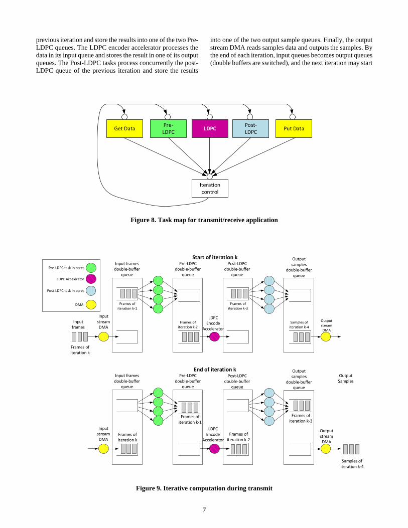
7
previous iteration and store the results into one of the two Pre-
LDPC queues. The LDPC encoder accelerator processes the
data in its input queue and stores the result in one of its output
queues. The Post-LDPC tasks process concurrently the post-
LDPC queue of the previous iteration and store the results
into one of the two output sample queues. Finally, the output
stream DMA reads samples data and outputs the samples. By
the end of each iteration, input queues becomes output queues
(double buffers are switched), and the next iteration may start
Get DataPre-LDPC
LDPCPost-LDPC
Put Data
Iterationcontrol
Figure 8. Task map for transmit/receive application
Input framesdouble-buffer
queue
Pre-LDPCdouble-buffer
queue
Input frames
LDPC Encode
Accelerator
Input stream DMA
Output stream DMA
Start of iteration kPost-LDPC
double-buffer queue
Output samples
double-buffer queue
Frames of iteration k
Frames of iteration k-1
Frames of iteration k-2
Frames of iteration k-3
Samples of iteration k-4
Input framesdouble-buffer
queue
Pre-LDPCdouble-buffer
queue
LDPCEncode
Accelerator
Input stream DMA
Output stream DMA
End of iteration kPost-LDPC
double-buffer queue
Output samples
double-buffer queue
Frames of iteration k
Frames of iteration k-1
Frames of iteration k-2
Frames of iteration k-3
Samples of iteration k-4
Output Samples
DMA
Pre-LDPC task in cores
LDPC Accelerator
Post-LDPC task in cores
Figure 9. Iterative computation during transmit
8
Core #0
Core #3Core #4
Core #7LDPC Encoder
(a) Unbalanced load on 8 cores
Core #0
Core #3Core #4
Core #7
(b) Fine grain and work distributionhelp to balance
the load on 8 cores
LDPC Encoder
Core #0
Core #3Core #4
Core #35
(c) Shorter iteration time on 36 cores
LDPC Encoder
Core #0
Core #7Core #8
Core #50
(d) Even shorter execution time
on 51 cores; higher parallelism
of both tasks
LDPC Encoder
Pre-LDPC task in cores
LDPC Accelerator
Post-LDPC task in cores
iteration time iteration time iteration time iteration time
Figure 10. Alternative schedules for load balancing
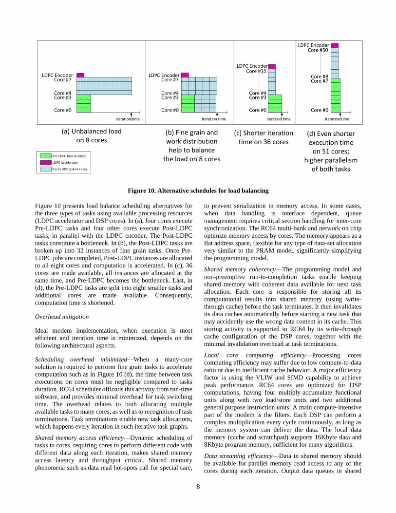
Figure 10 presents load balance scheduling alternatives for
the three types of tasks using available processing resources
(LDPC accelerator and DSP cores). In (a), four cores execute
Pre-LDPC tasks and four other cores execute Post-LDPC
tasks, in parallel with the LDPC encoder. The Post-LDPC
tasks constitute a bottleneck. In (b), the Post-LDPC tasks are
broken up into 32 instances of fine grain tasks. Once Pre-
LDPC jobs are completed, Post-LDPC instances are allocated
to all eight cores and computation is accelerated. In (c), 36
cores are made available, all instances are allocated at the
same time, and Pre-LDPC becomes the bottleneck. Last, in
(d), the Pre-LDPC tasks are split into eight smaller tasks and
additional cores are made available. Consequently,
computation time is shortened.
Overhead mitigation
Ideal modem implementation, when execution is most
efficient and iteration time is minimized, depends on the
following architectural aspects.
Scheduling overhead minimized—When a many-core
solution is required to perform fine grain tasks to accelerate
computation such as in Figure 10 (d), the time between task
executions on cores must be negligible compared to tasks
duration. RC64 scheduler offloads this activity from run-time
software, and provides minimal overhead for task switching
time. The overhead relates to both allocating multiple
available tasks to many cores, as well as to recognition of task
terminations. Task terminations enable new task allocations,
which happens every iteration in such iterative task graphs.
Shared memory access efficiency—Dynamic scheduling of
tasks to cores, requiring cores to perform different code with
different data along each iteration, makes shared memory
access latency and throughput critical. Shared memory
phenomena such as data read hot-spots call for special care,
to prevent serialization in memory access. In some cases,
when data handling is interface dependent, queue
management requires critical section handling for inter-core
synchronization. The RC64 multi-bank and network on chip
optimize memory access by cores. The memory appears as a
flat address space, flexible for any type of data-set allocation
very similar to the PRAM model, significantly simplifying
the programming model.
Shared memory coherency—The programming model and
non-preemptive run-to-completion tasks enable keeping
shared memory with coherent data available for next task
allocation. Each core is responsible for storing all its
computational results into shared memory (using write-
through cache) before the task terminates. It then invalidates
its data caches automatically before starting a new task that
may accidently use the wrong data content in its cache. This
storing activity is supported in RC64 by its write-through
cache configuration of the DSP cores, together with the
minimal invalidation overhead at task terminations.
Local core computing efficiency—Processing cores
computing efficiency may suffer due to low compute-to-data
ratio or due to inefficient cache behavior. A major efficiency
factor is using the VLIW and SIMD capability to achieve
peak performance. RC64 cores are optimized for DSP
computations, having four multiply-accumulate functional
units along with two load/store units and two additional
general purpose instruction units. A main compute-intensive
part of the modem is the filters. Each DSP can perform a
complex multiplication every cycle continuously, as long as
the memory system can deliver the data. The local data
memory (cache and scratchpad) supports 16Kbyte data and
8Kbyte program memory, sufficient for many algorithms.
Data streaming efficiency—Data in shared memory should
be available for parallel memory read access to any of the
cores during each iteration. Output data queues in shared
9
memory should be accessible efficiently and concurrently by
any of the cores for writing during each iteration. Streaming
data to and from shared memory queues must not degrade the
computing throughput. RC64 DMA controllers are optimized
for this purpose, both for memory buffer management in
shared memory and for very high throughput to and from
shared memory, without degrading memory access rate by
the cores. Many DMA controllers can operate concurrently
to serve many different I/O activities.
Programming model simplicity—Programming a many-core
processor can become a very complex undertaking, requiring
deep knowledge of the micro-architecture and the special
mechanisms for solving the above challenges. RC64 task
oriented programming model emphasize parallel code
decomposition for application acceleration, in accordance
with algorithm and memory capacity requirements. Other
issues, such as shared memory access efficiency, coherency
and streaming may incur only minor effect on performance,
while the application developer enjoys a PRAM-like
abstraction, similar to a single core program design.
5. PERFORMANCE
This section reports performance results as computed with
the RC64 DVB-S2 simulator and cycle-accurate simulations
of RC64 [8].
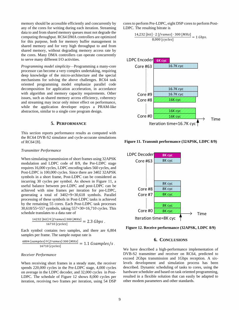
Transmitter Performance
When simulating transmission of short frames using 32APSK
modulation and LDPC code of 8/9, the Pre-LDPC stage
requires 16,000 cycles, LDPC encoding takes 560 cycles, and
Post-LDPC is 100,000 cycles. Since there are 3402 32APSK
symbols in a short frame, Post-LDPC can be considered as
incurring 30 cycles per symbol. As shown in Figure 11, a
useful balance between pre-LDPC and post-LDPC can be
achieved with nine frames per iteration for pre-LDPC,
generating a total of 3402×9=30,618 symbols. Parallel
processing of these symbols in Post-LDPC tasks is achieved
by the remaining 55 cores. Each Post-LDPC task processes
30,618/55=557 symbols, taking 557×30=16,710 cycles. This
schedule translates to a data rate of
14232 [𝑏𝑖𝑡]∙9 [𝑓𝑟𝑎𝑚𝑒𝑠]∙300 [𝑀𝐻𝑧]
16710 [𝑐𝑦𝑐𝑙𝑒𝑠]= 2.3 𝐺𝑏𝑝𝑠 .
Each symbol contains two samples, and there are 6,804
samples per frame. The sample output rate is
6804 [𝑠𝑎𝑚𝑝𝑙𝑒𝑠]∙9 [𝑓𝑟𝑎𝑚𝑒𝑠]∙300 [𝑀𝐻𝑧]
16710 [𝑐𝑦𝑐𝑙𝑒𝑠]= 1.1 𝐺𝑠𝑎𝑚𝑝𝑙𝑒𝑠/𝑠 .
Receiver Performance
When receiving short frames in a steady state, the receiver
spends 220,000 cycles in the Pre-LDPC stage, 4,000 cycles
on average in the LDPC decoder, and 32,000 cycles in Post-
LDPC. The schedule of Figure 12 shows 8,000 cycles per
iteration, receiving two frames per iteration, using 54 DSP
cores to perform Pre-LDPC, eight DSP cores to perform Post-
LDPC. The resulting bitrate is
14,232 [𝑏𝑖𝑡] ∙ 2 [𝑓𝑟𝑎𝑚𝑒𝑠] ∙ 300 [𝑀𝐻𝑧]
8,000 [𝑐𝑦𝑐𝑙𝑒𝑠]= 1 𝐺𝑏𝑝𝑠.
16K cycCore #0Time
Core #8Core #9
Core #63
Iteration time=16.7K cyc
16K cyc
LDPC Encoder16.7K cyc
6K cyc
16.7K cyc
16.7K cyc
16K cyc
Figure 11. Transmit performance (32APSK, LDPC 8/9)
8K cycCore #0Time
Core #7Core #8
Core #63
Iteration time=8K cyc
8K cyc
LDPC Decoder8K cyc
8K cyc
8K cyc
8K cyc
8K cyc
Figure 12. Receive performance (32APSK, LDPC 8/9)
6. CONCLUSIONS
We have described a high-performance implementation of
DVB-S2 transmitter and receiver on RC64, predicted to
exceed 2Gbps transmission and 1Gbps reception. A six-
levels development and simulation process has been
described. Dynamic scheduling of tasks to cores, using the
hardware scheduler and based on task oriented programming,
resulted in a flexible solution that can easily be adapted to
other modem parameters and other standards.
10
ACKNOWLEDGEMENT
Funding has been provided in part by Israel Space Agency
and by the European Union's Seventh Framework Program
for research and demonstration under grant agreement no.
607212 (MacSpace)
REFERENCES
[1] Ran Ginosar and Peleg Aviely, RC64 – Many-Core
Communication Processor for Space IP Router. In
Proceedings of International Astronautical Conference,
pp. IAC-15-B2.6.1. Jerusalem, Israel, Oct. 2015.
[2] DVB (2005). User guidelines for the second generation
system for Broadcasting, Interactive Services, News
Gathering and other broadband satellite applications
(DVB-S2). User guidelines ETSI TR 102 376 V1.1.1
(http://www.etsi.org).
[3] Morello, Alberto, and Vittoria Mignone. "DVB-S2: The
second generation standard for satellite broad-band
services." Proceedings of the IEEE, vol. 94, no. 1, pp.
210-227. IEEE, 2006.
[4] Nemer, Elias. "Physical layer impairments in DVB-S2
receivers." In Second IEEE Consumer Communications
and Networking Conference, CCNC, pp. 487-492. IEEE,
2005.
[5] Savvopoulos, Panayiotis, Nikolaos Papandreou, and Th
Antonakopoulos. "Architecture and DSP Implementation
of a DVB-S2 Baseband Demodulator." In Digital System
Design, Architectures, Methods and Tools, 2009.
DSD'09. 12th Euromicro Conference on, pp. 441-448.
IEEE, 2009
[6] Beadle, Edward R., and Tim Dyson. "Software-Based
Reconfigurable Computing Platform (AppSTAR TM) for
Multi-Mission Payloads in Spaceborne and Near-Space
Vehicles." In International Conference on Reconfigurable
Systems and Algorithms. ERSA 2012.
[7] Dalio, B. A., and K. A. Shelby. "The implementation of
OFDM waveforms on an SDR development platform
supporting a massively parallel processor." In SDR'09:
Proceedings of the Software Defined Radio Technical and
Product Exposition. 2009.
[8] Ginosar, Ran, Peleg Aviely, Tsvika Israeli and Henri
Meirov. “RC64: High Performance Rad-Hard
Manycore.” Aerospace Conference. IEEE, 2016.
BIOGRAPHY
Peleg Aviely received his BSc EE from
Ben Gurion University in Israel. He was
CTO and VP R&D of Plurality LTD, a
fabless semiconductor company that
developed many-core architecture for on-
chip parallel computing. He is an expert
on development of parallel embedded
system platforms and their parallel programming
model. Peleg serves as Senior Architect at Ramon Chips.
Olga Radovsky received her BSc EE from
Technical University of Moldova in 1995
and MSc in EE from the Technion—Israel
Institute of Technology in 2004. She
worked for Zoran Corporation as staff
algorithm engineer in demodulators R&D
group. She also worked for CSR as staff algorithm
engineer in digital camera R&D group. Olga serves as
Signal Processing Engineer at Ramon Chips.
Ran Ginosar received BSc in EE&CS
from the Technion—Israel Institute of
Technology in 1978 and PhD in EECS
from Princeton University in 1982. He
has conducted research at Bell
Laboratories, the University of Utah and
at Intel Research in Oregon. He has co-founded several
companies in the area of computing and
semiconductors. He is a professor at the Technion,
focusing on VLSI architecture, many-core architecture
and computing in space. Ran Ginosar is the CEO of
Ramon Chips.