Embed Size (px)
Citation preview
Joint Institute for Nuclear Research Bogoliubov Laboratory of Theoretical Physics
International Conference on Theoretical Physics
DUBNA-NANO2010
Book of abstracts
July 5-10, 2010 Dubna, Russia
Dubna 2010
УДК 538.9(063) ББК [22.31я431+22.37я431]
Organized by Bogoliubov Laboratory of Theoretical Physics of Joint Institute for Nuclear Research under the sponsorship of the Heisenberg - Landau Program of the
German Ministry for Science and Technology, the Russian Foundation for Basic Research and Bogoliubov-Infeld program
The contributions are reproduced directly from the originals presented by the Organizing Committee.
Dubna-Nano2010: Book of Abstr.of the Intern. Conf. (Dubna, July 5-10, 2010). — Dubna: JINR, 2010. — 161 p.
INTERNATIONAL ADVISORY COMMITTEE
T. Ando (TIT, Japan) J. Fabian (University of Regensburg, Germany) F. Guinea (ICMM, Spain) P. Hawrylak (IMS, Canada) K. Kadowaki (University of Tsukuba, Japan) T. Koyama (Tohoku University, Japan) Yu.I. Latyshev (IRE, Russia) Yu.E. Lozovik (IS, Russia) M. Machida (JAEA, Japan) B.K. Nikolić (University of Delaware, USA) N.F. Pedersen (TUD, Denmark) P.-G. Reinhard (Erlangen University, Germany) J.M. Rost (MPI-PKS, Germany) A.Ya. Vul’ (Ioffe Institute, Russia)
ORGANIZING COMMITTEE
V.A. Osipov - chairman V.O. Nesterenko - vice-chairman Yu.M. Shukrinov - vice-chairman S.E. Krasavin - scientific secretary T.S. Donskova - secretary O.G. Isaeva V.L. Katkov D.V. Kolesnikov A.N. Novikov
SPONSORS
Heisenberg - Landau program of the German Ministry for Science and Technology (BMBF)
Russian Foundation for Basic Research
Bogoliubov-Infeld program

5
CONTENTS
S. Adibi, S. Ziaei-Rad, F. Karimzadeh WEAR SIMULATION OF ALUMINUM-BASED METAL MATRIX NANOCOMPOSITE USING FINITE ELEMENT TECHNIQUE .................. 18
O. Adiguzel NANOSCALE CHARACTERIZATION OF MARTENSITE STRUCTURES IN COPPER BASED SHAPE MEMORY ALLOYS........................................... 19
I.O. Barinov, E. S. Sedov, A.V. Prokhorov, A.P. Alodjants, S.M. Arakelian SLOW LIGHT AND PHASE TRANSITION WITH STRONGLY LOCALIZED POLARITONS IN A ATOMIC MICRO-STRUCTURES ............................. 20
Kh.T. Kholmurodov, M.V. Altaisky, G.F. Aru, V.A. Krylov MOLECULAR DYNAMICS SIMULATIONS OF THE INTERACTION OF CARBON NANOTUBE WITH A CARBON DISULFIDE SOLVENT ......... 21
O. Yu. Andreeva, T. L. Boyadjiev, and Yu. M. Shukrinov CRITICAL DEPENDENCIES OF 0-K JOSEPHSON JUNCTIONS .............. 22
D.V. Anghel FRACTIONAL EXCLUSION STATISTICS IN SYSTEMS OF INTERACTING PARTICLES ................................................................................................. 23
P.Yu. Apel WHAT IS INTERESTING ABOUT TRACK-ETCHED NANOPORES? ...... 24
V. I. Artyukhov and L. A. Chernozatonskii GRAPHITE FLUORIDE AND GRAPHANE: STRUCTURE AND LAYER INTERACTIONS FROM COMPUTER SIMULATIONS.............................. 25
M. Balasoiu, G.M. Arzumanian, S.V. Stolyar, R.S. Iskhakov, L.A. Ishchenko, Yu.L. Raikher, D. V. Soloviov, T. S. Kurkin, A.V. Rogachev, O.I. Ivankov, J. Plestil, A. Meiszterics, L. Almasy, A.I. Kuklin BIOGENIC FERRIHYDRITE NANOPARTICLES STRUCTURE INVESTIGATIONS ...................................................................................... 26
A. Asgari THE EFFECTS OF POLARIZATION FIELDS ON EXCITON BINDING ENERGY IN GaN QUANTUM DOT............................................................ 27
A. Asgari THE SCATTERING OF HOT ELECTRONS BY PHONONS IN AlGaN/GaN QUANTUM DOT ......................................................................................... 28
6
P. Kh. Atanasova, T. L. Boyadjiev, E. V. Zemlyanaya, and Yu. M. Shukrinov INFLUENCE OF SECOND HARMONIC ON STABILITY OF MAGNETIC FLUX IN LJJ, DESCRIBED BY DOUBLE SINE-GORDON EQUATION ................................................................................................. 29
M. Balasoiu, I. Bica, Yu.L. Raikher, V.T. Lebedev, A.V. Rogachev, L. Almasy, J. Kohlbreher, N.S. Perov, E.B. Dokukin, and A.I. Kuklin MAGNETIC FIELD AND PARTICLE CONCENTRATION COMPETITIVE EFFECTS ON FERROFLUID BASED ELASTOMER MICROSTRUCTURE .................................................................................. 30
V.A. Belyakov, A.A. Konakov, N.V. Kurova, and V.A. Burdov RELAXATION PROCESSES IN DOPED SILICON NANOCRYSTALS ..... 31
I.V. Blinova, K.N. Kiz’yurova, and I.Yu. Popov NANOCONES ROLLING IN HYDRO-THERMAL MEDIUM AND FLOWS IN CONICAL DOMAINS.................................................................................. 32
Yu.V. Bludov, N. M. R. Peres, and M. I. Vasilevskiy SURFACE PLASMON-POLARITONS IN GRAPHENE LAYER: DISPERSION RELATION AND EXCITATION BY ATTENUATED TOTAL INTERNAL REFLECTION METHOD ............................................................................. 33
J.R. Castro Smirnov VERTICALLY ALIGNED CARBON NANOTUBES FOR MEAS APPLICATIONS .......................................................................................... 34
F. Cavaliere, E. Mariani, R. Leturcq, C. Stampfer, and M. Sassetti LOCAL FRANCK-CONDON FACTORS IN SUSPENDED CARBON NANOTUBE QUANTUM DOTS ................................................................. 35
R. Chauhan HIGH PRESSURE PHASE TRANSITION OF NOVEL MATERIALS ......... 36
L.A. Chernozatonskii NANOSTRUCTURES BASED ON HYDROGEN-FUNCTIONALIZED GRAPHENES AS MATERIALS FOR APPLICATIONS IN NANODEVICES .......................................................................................... 37
A.Yu. Cherny, E.M. Anitas, A.I. Kuklin, M. Balasoiu, and V.A. Osipov THE SCATTERING FROM GENERALIZED CANTOR FRACTALS ......... 38
A.V. Chizhov and R.G. Nazmitdinov AN ORBITAL ENTANGLEMENT IN TWO-ELECTRON QUANTUM DOTS IN A MAGNETIC FIELD ............................................................................. 39
7
O. Ciftja REALISTIC CONFINEMENT POTENTIAL FOR A SQUARE PATTERNED TWO-DIMENSIONAL SEMICONDUCTOR QUANTUM DOT AND ITS APPROXIMATED CIRCULAR COUNTERPART ....................................... 40
N. Shahtahmasebi, S.A. Ketabi, S. Dabagh, and A. Rashed Mohassel INFLUENCE OF VIBRATIONAL MODE ON THE ELECTRONIC PROPERTIES OF DNA MOLECULE IN LADDER MODEL....................... 41
M. Dineykhan, S. A. Zhaugasheva, and Zh. Bisarieva ENERGY SPECTRUM OF DIRAC ELECTRONS IN GRAPHENE QUANTUM DOTS ........................................................................................................... 42
A.B. Dubois PLASMA OSCILLATIONS AND ELECTRON-ELECTRON INTERACTIONS IN 2D ELECTRON SYSTEMS ..................................................................... 43
P. Elahi, A. Keshavarz, and M. Mehdipour THE EMISSION DIFFERENTIAL CROSS SECTION OF AN ELECTRON IN THE SEMIPARABOLIC QUANTUM WELL .............................................. 44
P. Elahi, M. Hooshmand THE PHOTOELECTRIC DIFFERENTIAL CROSS SECTION FOR A QUANTUM BOX WITH FINITE CONFINING ........................................... 45
R. Farghadan, A. Saffarzadeh, and E. Saievar Iranizad SPIN TRANSPORT THROUGH A TRIANGULAR GRAPHENE FLAKE ... 46
V.A. Fedirko, S.V. Polyakov, V.V. Vyurkov, and D.A. Zenyuk MODELING OF FIELD EMISSION FROM GRAPHENE ............................ 47
I. Fialkovsky, D. Vassilevich QUANTUM FARADAY EFFECT AND CASIMIR INTERACTION AS NEW QFT TEST IN GRAPHENE .......................................................................... 48
I. N. Filikhin, S. G. Matinyan, and B. Vlahovic NEIGHBOURING LEVELS STATISTIC FOR Si/SiO2 QUANTUM DOTS .................................................................. 49
D.A. Ivanov, Ya.V. Fominov, M.A. Skvortsov, and P.M. Ostrovsky EFFECTIVE SPIN-FLIP SCATTERING IN DIFFUSIVE SUPERCONDUCTING PROXIMITY SYSTEMS WITH MAGNETIC DISORDER .......................... 50
C. Gadermaier, J. Strle, M. Uplaznik, D. Vengust, B. Bercic, and D. Mihailovic MOSI NANOWIRES: FROM A ONE-DIMENSIONAL QUANTUM FLUID TO SELF-ORGANISED CRITICAL NETWORKS ....................................... 51
8
V. Galitski A GENERAL THEORY OF SPIN-RELAXATION IN TWO-DIMENSIONAL SEMICONDUCTORS .................................................................................. 52
S. Galović, Z. Šoškić, D. Čevizović THEORETICAL INVESTIGATION OF THE THERMAL CONDUCTIVITY OF NANOSTRUCTURES ............................................................................ 53
D. Čevizović, S. Galović, S. Zekovic, Z. Ivic CHARGE TRANSPORT IN THE α-HELIX PROTEINS............................... 53
A.J. Gelman and A.M. Satanin DISSIPATIVE DYNAMICS OF A SUPERCONDUCTING FLUX QUBIT DRIVEN BY A STRONG MICROWAVE FIELD ........................................ 54
A.V. Gets and V.P. Krainov INNER AND OUTER IONIZATION OF ATOMIC CLUSTERS BY AN INTENSE ATTOSECOND LASER PULSE.................................................. 55
L. Gharaee and A. Saffarzadeh EFFECTS OF MAGNETIC AND NONMAGNETIC IMPURITIES ON ELECTRONIC PROPERTIES OF SEMICONDUCTOR MULTILAYERS ... 56
B. Gharekhanlou and S. Khorasani BIPOLAR TRANSISTOR BASED ON GRAPHANE ................................... 57
B. Gharekhanlou and S. Khorasani LATTICE HEAT CAPACITY OF MESOSCOPIC NANOSTRUCTURES .... 58
Moshe Gitterman BROWNIAN MOTION WITH ADHESION ................................................. 59
O.E. Glukhova, I.N. Saliy, A.S. Kolesnikova, and M.M. Slepchenkov ELASTIC PROPERTIES OF GRAPHENE-GRAPHANE NANORIBBONS .......................................................................................... 60
E. Goldobin, S. Scharinger, C. Gürlich, R.G. Mints, M. Weides, H. Kohlstedt, D. Koelle, and R. Kleiner SUPERCURRENT INTERFERENCE PATTERNS IN MULTIFACET SIFS 0-π JOSEPHSON JUNCTIONS .......................................................................... 61
A. Goun THEORETICAL MODELS OF THE EXCITATION TRANSFER IN PHASE SEPARATING LIQUIDS ............................................................................. 62
9
D.D. Grachev and L.A. Sevastianov QUANTUM FIELD MODEL OF THE FERROMAGNETISM IN GRAPHENE STRUCTURES ............................................................................................. 63
A.A. Gusev, O. Chuluunbaatar, S.I. Vinitsky, E.M. Kazaryan, and H.A. Sarkisyan THE APPLICATION OF ADIABATIC METHOD FOR DESCRIPTION OF IMPURITY STATES IN QUANTUM NANOSTRUCTURES....................... 64
M. Hamdipour and Yu.M. Shukrinov STUDY OF CHARGE-PHASE AND CHARGE-CHARGE DIAGRAMS OF INTRINSIC JOSEPHSON JUNCTIONS ....................................................... 65
M. Hayashi, H. Yoshioka, and A. Kanda SUPERCONDUCTING PROXIMITY EFFECT IN GRAPHENE NANOSTRUCTURES .................................................................................. 66
K. Hirata, A. Thakur, and S. Ooi INTERMEDIATE VORTEX STATE IN NANO-SCALE ANTI-DOTS AND MESOSCOPIC SUPERCONDUCTORS ....................................................... 67
A. Irie, Y. Saito, M. Sakashita, K. Yamada, and G. Oya DETECTION OF THz RADIATION FROM INTRINSIC JOSEPHSON JUNCTIONS ................................................................................................ 68
J. Jang and L.C. Saha SURFACE DEPOSITION AND DEFORMATION OF CARBON NANOTUBE VIA COLLISION ......................................................................................... 69
E. S. Kadantsev, M. Zielinski, M. Korkusinski, and P. Hawrylak THEORY OF ELECTRON-HOLE EXCHANGE IN SEMICONDUCTOR QUANTUM DOTS ....................................................................................... 70
Mikhail S. Kalenkov, Dmitri S. Golubev, and Andrei D. Zaikin CROSSED ANDREEV REFLECTION IN MULTITERMINAL SUPERCONDUCTING HYBRID STRUCTURES........................................ 71
V.L. Katkov and V.A. Osipov GEOMETRIC SHAPE EFFECTS ON FIELD EMISSION FOR AXISYMMETRIC AND WALL-LIKE EMITTERS.................................................................... 72
M. Kato, O. Sato, T. Koyama, M. Machida, and T. Ishida VORTEX DYNAMICS IN FINITE SUPRECONDUCTING NETWORKS AND COMPOSITE STRUCTURES OF D- AND S-WAVE SUPERCONDUCTORS (D-DOT) ....................................................................................................... 73
10
S. Kawabata, Y. Asano, S. Kashiwaya, Y. Tanaka, and A. A. Golubov ATOMIC-SCALE 0-π TRANSITION IN A SUPERCONDUCTOR/ FERROMAGNETIC-INSULATOR HETEROSTRUCTURE ........................ 74
R. Kerner AGGLOMERATION MODEL OF CARBON NANOSTRUCTURES ........... 75
R.A. Khan and V. Rai NANOPARTICLE SIZING AND LATE STAGE FUSION DURING MATRIX DIFFUSION: A MATHEMATICAL MODELING STUDY .......................... 76
M.M. Khapaev and M.Yu. Kupriyanov SHEET CURRENT MODEL FOR INDUCTANCES EXTRACTION AND JOSEPHSON JUNCTIONS DEVICES SIMULATION ................................. 77
Yu.N. Khaydukov, K.N. Zhernenkov, Yu.V. Nikitenko, B. Nagy, L. Bottyan, R. Steitz, A. Teichert, A. Rühm, and V.L. Aksenov EXPERIMENTAL OBSERVATION OF THE INVERSE PROXIMITY EFFECT IN THE SUPERCONDUCTOR/FERROMAGNET BILAYER...................... 78
R. Kheradmand, M. Eslami CAVITY SOLITON MOBILITY IN SEMICONDUCTOR MICRORESONATORS ABOVE LASER THRESHOLD.................................................................... 79
R. Kheradmand and H. Aryan STUDY OF ALL OPTICAL SWITCHING BEHAVIOR IN SEMICONDUC- TOR MICRORESONATOR WITH NANO-ACTIVE LAYER ...................... 80
D.V. Khveshchenko MASSIVE DIRAC FERMIONS IN GRAPHENE ......................................... 81
M.A. Kiselev LIPID NANOSTRUCTURES ....................................................................... 82
A.L. Klavsyuk, S.V. Kolesnikov, and A.M. Saletsky STRUCTURE, QUANTUM EFFECTS AND MAGNETISM IN Pd CONTACTS ............................................................... 83
R. Kleiner, S. Guénon, B. Gross, M. Grünzweig, D. Koelle, H. Wang, J. Yuan, A. Iishi, T. Hatano, Z. Jiang, Y. Zhong, and P. Wu IMAGING HOT SPOTS AND THz WAVES IN INTRINSIC JOSEPHSON JUNCTIONS ................................................................................................ 84
11
A.V. Kleshchonok INSTABILITY OF THE NEMATIC LIQUID CRYSTAL FILLED WITH SPHERE-LIKE MAGNETIC-IMPURITY PARTICLES AGAINST FORMA- TION OF THE MODULATED STRUCTURES ............................................ 85
A.M. Klushin, F. Song, A.D. Semenov and V.V. Kurin TOWARDS TERAHERTZ JOSEPHSON RADIATION SOURCES: RECENT RESULTS..................................................................................................... 86
A. Kokabi, M. Hoseini, A. Moftakharzadeh, M. A. Vesaghi, and M. Fardmanesh PHOTONIC BAND STRUCTURE CALCULATION AND OPTICAL ABSORPTION MODELING OF THE COPPER CARBON COMPOSITE NANOLAYER BASED ON THE 3D LATTICE OF COUPLED DIPOLES .. 87
M. Hamdipour, M. R. Kolahchi, and Yu.M. Shukrinov CHARACTERIZATION OF THE CHAOTIC DYNAMICS IN THE I-V OF THE STACKED ARRAY OF JOSEPHSON JUNCTIONS ............................ 88
Yu.A. Kolesnichenko, Ye.S. Avotina, and J.M. van Ruitenbeek MAGNETO-ORIENTATION AND QUANTUM SIZE EFFECT IN SP-STM CONDUCTANCE IN THE PRESENCE OF A SUBSURFACE MAGNETIC CLUSTER .................................................................................................... 89
D.V.Kolesnikov and V.A.Osipov SCATTERING OF ELECTRONS ON THE DISCLINATION DIPOLE IN METALLIC NANOTUBES .......................................................................... 90
S.V. Kolesnikov, A.L. Klavsyuk, and A.M. Saletsky RIPENING OF MONOLAYER VACANCY PITS IN Co THIN FILM ON Cu(100) SURFACE ...................................................................................... 91
V.N. Kondratyev DYNAMICS OF MAGNETIC NANOPARTICLE ASSEMBLY ................... 92
V.N. Kondratyev MAGICS FOR MAGNETIZED FERMI DROPLETS.................................... 93
V.R. Kornev, I.I. Soloviev, N.V. Klenov, and O.A. Mukhanov PROGRESS IN HIGH-LINEARITY SQIF STRUCTURES ........................... 94
N.V. Klenov, A.V. Sharafiev, V.K. Kornev, and S.V. Bakursky SUPERCONDUCTING QUANTUM BIT STATE EVOLUTION UNDER DETERMINED EXTERNAL FORCE .......................................................... 94
12
Z.Ya. Kosakovskaya, Yu.I. Latyshev, A.P. Orlov, and G.G. Kosakovskii THE STUDY OF CHARGE TRANSPORT THROUGH DENSE STRUCTURES OF ORIENTED CARBON NANOTUBES .................................................... 95
G.G. Kosakovskii, M.M. Simunin, V.K. Nevolin, Z.Ya. Kosakovskaya, and A.M. Smolovich THE STUDY OF FORMATION CONDITIONS OF CARBON FILMS WITH DIFFERENT STRUCTURE DIMENSIONAL .............................................. 96
A. Koshelev DYNAMIC KINK STATES IN INTRINSIC JOSEPHSON JUNCTIONS GENERATED BY INTERNAL RESONANCE............................................. 97
T. Koyama, Y. Ota, and M. Machida ELECTRODYNAMICS AND INTRINSIC JOSEPHSON EFFECTS IN MULTI-GAP SUPERCONDUCTORS ....................................................................... 98
S.E. Krasavin MOBILITY IN EPITAXIAL GaN: LIMITATION OF ELECTRON TRANSPORT DUE TO DISLOCATION WALLS ........................................ 99
E.S. Kryachko THE MAGIC GOLD CLUSTER Au20(TD) AND ITS LOW-ENERGY FULLERENE-TYPE ISOMERS ................................................................... 100
A.I. Kuklin, A.V. Rogachev, A.Yu. Cherny, T.N. Murugova, E.B. Dokukin, O.I. Ivankov, Yu.S. Kovalev, D.V. Soloviev, P.K.Utrobin, A.G. Soloviev, and V.I. Gordeliy NANOSCALE SIZE EFFECTS .................................................................... 101
F.V. Kusmartsev PERSPECTIVES OF SUPERCONDUCTING NANO-ELECTRONICS ........ 102
Yu.I. Latyshev, A.P. Orlov, A.Yu. Latyshev, W. Escoffier, and P. Monceau DIRAC FERMIONS IN GRAPHITE NANOSTRUCTURES ........................ 103
N.A. Lebedeva and L.S. Moiseeva THE INFLUENCE OF CARRIER GAS TYPE ON THE YIELD OF LONG VERTICAL WELL-ALLIGNED CARBON NANOTUBES .......................... 104
Gil-Ho Lee, Yong-Duk Jin, and Hu-Jong Lee COLLECTIVE THERMAL AND QUANTUM DEPINNING OF A ROW OF JOSEPHSON-VORTEX CHAINS IN NATURALLY STACKED HIGH-TC JOSEPHSON JUNCTIONS .......................................................................... 105
13
K.P. Katin, D.A. Lobanov, and M.M. Maslov THERMAL STABILITY OF THE PLATONIC HYDROCARBONS AND FULLERENES ............................................................................................. 106
Yu.E. Lozovik COHERENT PHASES IN GRAPHENE AND GRAPHENE BASED NANOSTRUCTURES .................................................................................. 107
M. Machida, N. Sasa, T. Koyama, and H. Matsumoto ELECTROMAGNETIC WAVE EMISSION AND REFLECTION IN JOSEPHSON JUNCTIONS; AN ANALYTICAL APPROACH .................... 109
A.I. Mese, P. Capuzzi, Z. Akdeniz, and S.E. Okan DENSITY PROFILES AND INERTIA MOMENTS OF INTERACTING BOSONS IN ANISOTROPIC HARMONIC CONFINEMENT ..................... 110
A. Mikaberidze ULTRAFAST FORMATION OF A RESONANT NANOPLASMA IN DOPED HELIUM DROPLETS .................................................................................. 111
A.H. Mohammadzaheri, P. Nooraliei, and A. Ali Zolanvari CALCULATION OF ENERGY EIGEN VALUE FOR NANO-WIRES ......... 112
W. Nawrocki PHYSICAL LIMITS FOR SCALING OF INTREGRATED CIRCUITS ........ 113
R.G. Nazmitdinov and K.N. Pichugin SPIN-ORBIT EFFECTS IN SEMICONDUCTOR NANOSTRUCTURES IN A MAGNETIC FIELD ..................................................................................... 114
A.M. Nemilentsau, G.Ya. Slepyan , and S.A. Maksimenko RABI OSCILLATIONS AND SATURABLE ABSORPTION EFFECT IN SINGLE-WALL CARBON NANOTUBES ................................................... 115
A.M. Nemilentsau, M.V. Shuba, P.N. D’yachkov, G.Ya. Slepyan, P.P. Kuzhir, and S.A. Maksimenko TERAHERTZ RADIATION ABSORPTION BY THE COMPOSITES CONTAINING CHEMICALLY MODIFIED CARBON NANOTUBES ....... 116
V.O. Nesterenko, A.N. Novikov, A.Yu. Cherny, and E. Suraud TRANSPORT OF TRAPPED ATOMS AND CONDENSATES .................... 117
14
Branislav K. Nikoli ć GRAPHENE NANORIBBONS FAR FROM EQUILIBRIUM: FUNDAMENTALS, COMPUTATIONAL ALGORITHMS, AND NANOELECTRONICS APPLICATIONS..................................................... 118
M. Okumura, H. Onishi, S. Yamada, and M. Machida ANOMALOUS NON-EQUILIBRIUM ELECTRON TRANSPORT IN ONE-DIMENSIONAL QUANTUM NANO WIRE AT HALF-FILLING: TIME DEPENDENT DENSITY MATRIX RENORMALIZATION GROUP STUDY........................................................................................... 119
Y. Ota, M. Machida, and T. Koyama THEORY OF JOSEPHSON EFFECTS IN IRON-BASED MULTI-GAP SUPERCONDUCTOR JUNCTIONS ............................................................ 120
L. Ozyuzer, F. Turkoglu, H. Koseoglu, Y. Demirhan, Z. Meric, Y. Simsek,
C. Kurter, U. Welp, K. E. Gray, T. Yamamoto, K. Kadowaki, H.B. Wang, and P. Müller FINE SPECTRAL FEATURES IN TERAHERTZ WAVE EMITTING Bi2Sr2CaCu2O8+d MESAS.............................................................................. 121
Pouya Partovi-Azar, Afshin Namiranian THE EFFECT OF THE ORIENTATION OF STONE-WALES DEFECTS ON THE NONLINEAR CONDUCTANCE OF CARBON NANOTUBES ........... 122
V.A. Pavlov “INTEGRAL” AND “DIFFERENTIAL” CHEMICAL POTENTIALS A ND THEIR ROLE IN THE THEORY OF PHASE TRANSITIONS IN ATOMIC CLUSTERS .................................................................................. 123
A.N. Pechen CONTROL OF NANOSCALE OPEN QUANTUM SYSTEMS .................... 124
R.G. Nazmitdinov, K.N. Pichugin SUPPRESSION OF SPIN-PRECESSION DUE TO RASHBA AND DRESSELHAUS SPIN-ORBIT INTERACTION BY IN-PLANE MAGNETIC FIELD .......................................................................................................... 125
M. Pudlak, R. Pincak INFLUENCE OF THE MAGNETIC FIELD ON THE ELECTRONIC SPECTRA OF DOUBLE-WALL CARBON NANOTUBE............................ 126
F. Cavaliere, G. Piovano, F. Haupt, M. Merlo, E Paladino and M. Sassetti SUB-POISSONIAN PHONONIC POPULATIONS IN A NANOELECTROMECHANICAL SYSTEM ................................................ 127
15
V.E. Egorushkin, N.V. Melnikova, and A.N. Ponomarev OXYGEN ADSORPTION IN CARBON NANOTUBES............................... 128
M. Pons and A. Puente EFFICIENT SPIN PROJECTION IN HARTREE-FOCK CALCULATIONS ........................................................................................ 129
I.Yu. Popov, S.A. Chivilikhin, V.V. Gusarov and I.V. Blinova MODEL OF FLUID FLOW IN NANOTUBE: CLASSICAL AND QUANTUM FEATURES.............................................................................. 130
A. Puente, M. Pons, and R.G. Nazmitdinov INTERACTION EFFECTS IN QUANTUM DOTS IN A MAGNETIC FIELD .................................................................................. 131
Y.M Shukrinov, I.R. Rahmonov, and M. El Demery PECULIARITIES OF PHASE DYNAMICS OF COUPLED JOSEPHSON JUNCTIONS IN CCJJ AND CCJJ+DC MODELS ........................................ 132
N. Shahtahmasebi, A. Rashed Mohassel, S. Ahamad Ketabi, and S. Dabagh ENVIRONMENTAL EFFECTS ON ELECTRIC PROPERTIES OF DNA MOLECULE ................................................................................................ 133
P.-G. Reinhard, B. Faber, P. Wopperer, P.M. Dinh, and E. Suraud CLUSTERS IN CONTACT WITH SUBSTRATES - THE EFFECT OF THE INTERFACE ON CLUSTER DYNAMICS ................................................... 134
V.E. Egorushkin, N.V. Melnikova, A.N. Ponomarev, and A.A. Reshetnyak ANOMALOUS THERMAL CONDUCTIVITY IN MULTIWALLED CARBON NANOTUBES WITH IMPURITIES ............................................ 135
Mahdi Sargolzaei and Farideh Gudarzi MAGNETIC PROPERTIES OF TRANSITION METALS (3D) ADD ON GRAPHENE: A DENSITY FUNCTIONAL STUDY .................................... 136
Mahdi Sargolzaei and Samaneh Ataee ORBITAL MAGNETISM IN 3D TRANSITION METAL NANOWIRES (Fe,Co,Mn): A DENSITY FUNCTIONAL STUDY....................................... 137
N.G. Aghekyan, E.M. Kazaryan, and H.A. Sarkisyan TWO ELECTRONIC STATES IN LAYERED QUANTUM DOTS .............. 138
M.V. Denisenko, A.M. Satanin, S. Ashhab, and F. Nori AMPLITUDE SPECTROSCOPY OF TWO COUPLED JOSEPHSON QUBITS ................................................................................. 139
16
Alexander Grib, Yury Shukrinov, Frank Schmidl, and Paul Seidel EXPERIMENTAL AND THEORETICAL INVESTIGATION ON HIGH-TC SUPERCONDUCTING INTRINSIC JOSEPHSON JUNCTIONS ................. 140
Alexander Grib and Paul Seidel THE ORIGIN OF MULTIBRANCH IV-CHARACTERISTICS OF SHUNTED JOSEPHSON JUNCTION ARRAYS.......................................... 141
A.G. Semenov and A.D. Zaikin FLUCTUATIONS OF PERSISTENT CURRENT ......................................... 142
Ll. Serra QUANTUM WIRES AND TWO-DIMENSIONAL ELECTRON GASES WITH INHOMOGENEOUS RASHBA INTERACTION .............................. 143
M. Ashhadi, N. Shahtahmassebi, M. Askari, and D. Vahedi TUNNEL MAGNETORESISTANCE OF AN ORGANIC MOLECULE JUNCTION .................................................................................................. 144
M. Askari, N. Shahtahmassebi, D. Vahedi, and M. Ashhadi TUNNELING MAGNETORESISTANCE OF POLYACENE-BASED MAGNETIC JUNCTION.............................................................................. 145
G.V. Shpatakovskaya FIELD-EMISSION CURRENT FROM QUANTUM SYSTEM ..................... 146
Yu.M.Shukrinov and M.Hamdipour LONGITUDINAL PLASMA WAVE NUCLEATION IN COUPLED SYSTEM OF JOSEPHSON JUNCTIONS ..................................................... 147
Yu.A. Sitenko QUANTUM SCATTERING ON VORTICES IN NANOPHYSICS ............... 148
Veronika V. Dick, Ilia A. Solov’yov, and Andrey V. Solov’yov NANOPARTICLES DYNAMICS ON A SURFACE: FRACTAL PATTERN FORMATION AND FRAGMENTATION .................................................... 149
Dmitri B. Strukov COUPLED IONIC AND ELECTRONIC TRANSPORT MODEL OF THIN- FILM SEMICONDUCTOR NANODEVICES............................................... 150
J. Messud, P. M. Dinh, E. Suraud, and P. G. Reinhard THE SELF INTERACTION CORRECTION REVISITED ............................ 151
17
V.L. Aksenov, T.V. Tropin, M.V. Avdeev KINETICS OF CLUSTER GROWTH IN FULLERENE C60 SOLUTIONS IN NITROGEN-CONTAINING SOLVENTS .................................................... 152
V.V. Tugushev PROXIMITY INDUCED SPIN ORDERING AT THE FERROMAGNETIC METAL/DILUTE MAGNETIC SEMICONDUCTOR INTERFACE ............. 153
A.V. Bunyakin and A.A. Vasilchenko PHASE DIAGRAM OF THE BILAYER SYSTEM AT 1=ν ....................... 154
N.D. Vlasii DENSITY OF ELECTRONIC STATES IN GRAPHENE WITH IMPURITIES ..................................................................................... 155
A.Ya. Vul’ DETONATION NANODIAMONDS AS A NEW CARBON NANO- STRUCTURE FOR NANOTECHNOLOGY. ................................................ 156
H. B. Wang, S. Guenon, J. Yuan, Z. G. Jiang, Y. Y. Zhong, P. H. Wu, A. Iishi, T. Hatano, B. Gross, M. Gruenzweig, D. Koelle, and R. Kleiner TERAHERTZ EMISSION FROM INTRINSIC JOSEPHSON JUNCTIONS AT HIGH BIAS AND LOW BIAS ................................................................ 157
Yu. Yamauchi and P. Yu. Apel THE EFFECT OF SURFACTANTS ON CHEMICAL DEVELOPMENTS OF ION TRACKS IN POLYMERS .................................................................... 158
V.I. Yukalov and E.P. Yukalova QUANTUM DOT SUPERRADIANT EMISSION ........................................ 159
A.D. Zaikin SHOT NOISE AND COULOMB BLOCKADE OF ANDREEV REFLECTION ........................................................................... 160
A. Zolanvari, H. Sadeghi, R. Pormusavi, and J. Nezamdost NANOSTRUCTURE AND MAGNETIC PROPERTIES OF Ni/Cu MULTILAYERS .......................................................................................... 161
18
WEAR SIMULATION OF ALUMINUM-BASED METAL MATRIX NANO-COMPOSITE USING FINITE ELEMENT TECHNIQUE
S. Adibi, S. Ziaei-Rad, F. Karimzadeh
Mechanical Engineering Department, Isfahan University of Technology, Iran
E-mail: [email protected]
Aluminum-based metal matrix nano-composites are known as eminent materials for structural application in the aircraft and automotive industries because they not only exhibit relatively better mechanical characteristics in comparison with other allay, but their cost of component production is comparatively low. Moreover, it is widely known that this kind of materials displays noticeable improvement in wear resistance compared to unreinforced alloys. In operating conditions, components made of Al-based composites are usually subjected to elevated temperatures and high contact loads, and hence are accordingly widely used to fabricate mechanical parts that are involved in sliding contact. Subsequently, prediction and experimental determination of their wear properties is of special importance and significance. Ex-perimental determination of life parameters in terms of wear has both a cost and time impact. Consequently, the ability to predict wear at the development stage ena-bles the designers to come up with a better design, longer useful life and more relia-ble products. Despite the marked interest, the simulation of wear is still in its early stages due to its complexity. In the present study, a series of pin on disk test on Al-Mg-Si/Al2O3 nanocomposites and the corresponding unreinforced alloy has been carried out at different loads and sliding distances. In addition, a finite element mod-el to simulate wear tests was developed. The number of operating cycles which is required to predict the wear simulation and eventually the life span of such materials falls in the range of several hundreds of thousands. Thus, an FE post processor looks the optimum choice regarding the computational expense of such large deformable-deformable contact simulations. Our approach is to extract the stress-strain curve for nanocomposite using a unit cell approach in conjugation with finite element. Next, a wear model based on Archard’s wear law in an FE post-processor that works in as-sociation with commercial FE package ANSYS for solving the general deformable-deformable contact problem is developed. According to this model, local wear is computed and then integrated over the sliding distance using the Euler integration scheme. After every wear step the geometry is re-meshed to correct the deformation due to wear. The wear on both the pin and disc surface are computed using the con-tact pressure distribution evaluated from a two dimensional FE model of the pin and disk included Coulomb friction at the contact. The validity of the simulation results has been verified by a series of experiments. Experiments were conducted on a POD rig to measure the friction coefficient as well as the wear depth, two parameters which are needed for the simulation The simulation results are in good agreement with those measured from the experiment.
19
NANOSCALE CHARACTERIZATION OF MARTENSITE STRUCTURES IN COPPER BASED SHAPE MEMORY ALLOYS
O. Adiguzel
Department of Physics, Firat University, 23169 Elazig, Turkey
E-mail: oadigü[email protected]
Martensitic transformations are first order displacive transitions and occur in the materials on cooling from high temperature. Shape memory effect is an unusual property exhibited by certain alloy systems, and leads to martensitic transition. If these alloys are deformed in martensitic condition, they keep the deformed shape, when the stress is removed, the deformation disappears and the material returns to the original phase on heating over the austenite finish temperature.
Copper-based alloys exhibit this property in beta phase field which possess sim-ple bcc - structures, austenite structure at high-temperatures. As temperature is low-ered the austenite undergoes martensitic transition following two ordering reactions, and structural changes in nanoscale govern this transition. The formation of the lay-ered structures in copper based alloys consists of shears and shear mechanism.
Martensitic transformations occur in a few steps with the cooperative movement of atoms less than interatomic distances by means of lattice invariant shears on a 110 - type plane of austenite matrix which is basal plane or stacking plane of mar-tensite.
First one is Bain distortion which is a homogeneous distortion of the bcc based B2 lattice, consisting of an elongation in the Bain direction parallel to a [001] direc-tion and a compression in the plane normal to it, until the B2 lattice becomes face centred cubic. Second one is homogeneous shears, lattice invariant shears which occur on a 110-type close packet plane of austenite matrix. The lattice invariant shears occurs, in two opposite directions, <110> -type directions on the 110-type plane. These shears gives rise to the formation of layered structure.
The beta-type martensites occur as orthorhombic close-packed structures, which consist of an array of close-packed planes. Defects in the regular sequence of atomic planes can be frequently met in crystalline materials; quantity and sequence of this kind of defects influence the properties and behaviour of the material itself.
Product phase in this transition has the unusual layered structures which consist of an array of close-packed planes with complicated stacking sequences called as 3R, 9R or 18R martensite structures depending on the stacking sequences on 110- type planes of parent phase. Monoclinic distortion takes place in some cases and 18R structure is modified as M18R.
In the present contribution, x-ray diffraction and transmission electron microsco-py studies were carried out on two copper based CuZnAl and CuAlMn alloys.
Keywords: Martensitic transition, shape memory effect, Bain distortion, layered structures.
20
SLOW LIGHT AND PHASE TRANSITION WITH STRONGLY LOCAL-IZED POLARITONS IN A ATOMIC MICRO-STRUCTURES
I.O. Barinov, E. S. Sedov, A.V. Prokhorov, A.P. Alodjants, S.M. Arakelian
Department of Physics and Applied Mathematics, Vladimir State University, Gorkogo str. 87, Vladimir, 600000 Russia
E-mail: [email protected]
For the last decade great efforts have been made in laser field manipulation of large number of ultracold atomic ensembles. In particular, the macroscopic array of atomic condensates produced by trapping, cooling and localization of atoms under the Bose-Einstein condensation (BEC) condition in one and/or two dimensional op-tical lattices gives an opportunity to study various aspects of physics of phase transi-tions. On the other hand, current nanofabrication and nanophotonic technologies make it possible to build up similar structures using array of photonic cavities (or coupled resonator waveguides) doped by two level atoms. The key role in behavior of such systems is played by so-called dark and bright polaritons, i.e. Bosonic qua-siparticles representing a linear superposition of photons in external (probe) field and macroscopic (coherent) excitations of two-level atomic system.
In the present paper (see also [1,2]) we propose a new type of spatially periodi-cal structure - polaritonic crystal (PolC), to observe a slow light phenomenon due to coupled atom-field states (polaritons) in the lattice. Under the tight-binding approx-imation such a system realizes an array of weakly coupled trapped two-component atomic ensembles interacting with optical field in a tunnel-coupled one dimensional cavity array. We have shown that the phase transition to the superfluid state of low branch polaritons occurs under the strong coupling condition. Such a transition re-sults in the appearance of a macroscopic polarization of atomic medium at non-zero frequency. The principal result is that the group velocity of polaritons is essentially depended on the order parameter of the system, i.e. on the average photon number in the cavity array. We have shown that for propagation of optical wave packet in the PolC structure the phenomenon of stopped light is also observed and the coherently stored information process can be realized on macroscopic atomic excitations. The group velocity of the polaritons in this case can be smoothly controlled by using detuning of atom-filed system.
References
[1]. I.O. Barinov, A.P. Alodjants, S.M. Arakelian, Rus. J. Quantum Electronics, 39, p.685 (2009) [2] A P Alodjants, I O Barinov, S M Arakelian, J. Phys. B: At. Mol. Opt. Phys. 43 095502 (2010).
21
MOLECULAR DYNAMICS SIMULATIONS OF THE INTERACTION O F CARBON NANOTUBE WITH A CARBON DISULFIDE SOLVENT
Kh.T. Kholmurodov, M.V. Altaisky, G.F. Aru, V.A. Krylov
Joint Institute for Nuclear Research, 141980, Dubna, Moscow region, Russia International University “Dubna”, 141980, Dubna, Moscow region, Russia
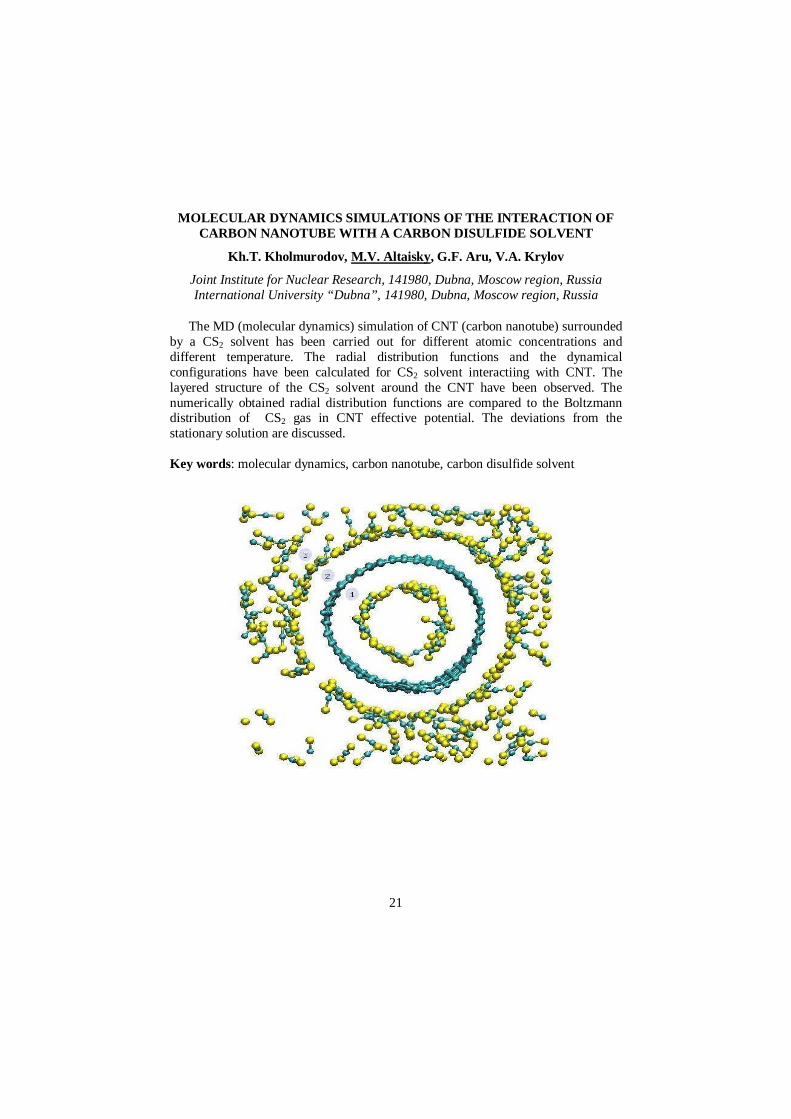
The MD (molecular dynamics) simulation of CNT (carbon nanotube) surrounded by a CS2 solvent has been carried out for different atomic concentrations and different temperature. The radial distribution functions and the dynamical configurations have been calculated for CS2 solvent interactiing with CNT. The layered structure of the CS2 solvent around the CNT have been observed. The numerically obtained radial distribution functions are compared to the Boltzmann distribution of CS2 gas in CNT effective potential. The deviations from the stationary solution are discussed. Key words: molecular dynamics, carbon nanotube, carbon disulfide solvent
22
CRITICAL DEPENDENCIES OF 0-K JOSEPHSON JUNCTIONS
O. Yu. Andreeva1 , T. L. Boyadjiev 2 , and Yu. M. Shukrinov 2
1 OAO "Teplo Tyumeni", Tyumen, 625023, Russia 2 JINR, 141980 Dubna, Moscow Region, Russia
E-mail: [email protected]
The −π Josephson junctions and more complex structure like parallel series of k−0 Josephson junctions attract much attention in the last time [1,2]. In this paper
we present the results of numerical modeling of the dependence "critical current-external magnetic field" for k−0 Josephson junctions. Each solution (distribution of the magnetic flux in the junction) is associated to a Sturm–Liouville problem and the stability of the static solutions is investigated by checking the sign of the smallest eigenvalue of this Sturm-Liouville problem. At each step of numerical calculation, the corresponding nonlinear boundary problem is solved on the basis of the continuous analog of Newton's method. The transitions between different distributions of magnetic flux with increase in k are demonstrated. We observe a creation of pure and mixed chains of fluxons and antifluxons with increase in intensity of external magnetic field and external current.
References
[1] J.Pfeiffer, M.Kemmler, D.Koelle, R.Kleiner, E.Goldobin, M.Weides, A.K.Feofanov, J.Lisenfeld, and A.V.Ustinov Phys. Rev. B., 77, 214506 (2008) [2] K.Buckenmaier, T.Gaber, M.Siegel, D.Koelle, R.Kleiner, E.Goldobin, Phys.Rev.Lett., 98, 117006 (2007)
23
FRACTIONAL EXCLUSION STATISTICS IN SYSTEMS OF INTERACTING PARTICLES
D. V. Anghel
Department of Theoretical Physics. National Institute of Physics and Nuclear Engineering. Str. Atomistilor no.407, P.O.BOX MG-6, RO-077125
Magurele, Jud. Ilfov, ROMANIA
E-mail: [email protected], Web page: http://www.theory.nipne.ro/ dragos/
In [1] Haldane introduced the fruitful concept of fractional exclusion statistics (FES). One of the most influential papers in which the thermodynamics of FES systems was deduced is [2]. Nevertheless, in [3,4] I showed that some important properties of the exclusion statistics parameters--namely the transformation properties of the FES parameters at the change of particle species--were overlooked in the original paper [1] and in all the papers after that, including [2]. Because of this omission, the implementation of FES into concrete physical systems remained, to a certain degree, arbitrary and the thermodynamic results were eventually not well defined.
In this presentation I will make a brief introduction into the FES formalism and its properties, pointing out the recent developments. I will also show that FES is manifesting in general in mesoscopic systems and I will give a general method for the calculation of the FES parameters. I will apply the method to concrete physical systems and calculate their thermodynamics. I will point out the features that appear in the thermodynamics of these systems due to the manifestation of FES and make comparisons with the typical Bose and Fermy gases.
References
[1] F. D. M. Haldane, Phys. Rev. Lett. 67, 937 (1991). [2] Yong-Shi Wu, Phys. Rev. Lett. 73, 922 (1994). [3] D. V. Anghel, J. Phys. A: Math. Theor., 40, F1013 (2007); arXiv:0710.0724. [4] D. V. Anghel, EPL, 87, 60009 (2009); arXiv:0906.4836.
24
WHAT IS INTERESTING ABOUT TRACK-ETCHED NANOPORES?
P.Yu. Apel1,2
1Flerov Laboratory of Nuclear Reactions, JINR, 141980 Dubna, Russia 2International University "Dubna", Universitetskaya, 19, 141980, Dubna, Russia
E-mail: [email protected], Web page: http://flerovlab.jinr.ru/
The use of synthetic nanopores for single-molecule sensing, biomimetic systems, separation processes, and nanofluidic devices attracts a great deal of interests of sci-entists from various fields [1]. Considerable research activity has been focused on the nanometer-sized ion track pores in polymers in recent years. Conical ion track nanopores have been developed to approach the geometric characteristics of the ion channels in living matter [2,3]. It has been demonstrated that the conical nanopores in polymers such as polyethylene terephthalate are cation selective and possess di-ode-like voltage-current characteristics in electrolyte solutions.
Recently we developed a novel fabrication method which allows production of ion track membranes (ITMs) with pronounced geometrical asymmetry and highly-tapered nanopore tip (“bullet-like” shape). It was shown that the rectification proper-ties of the asymmetric ITMs strongly depend on the pore profile [4,5]. Control over the shape of nanochannels may shed light on the mechanism responsible for their intriguing properties and opens the way to new potential applications of ITMs.
References
[1] C. Dekker. Solid state nanopores. Nat. Nanotechnology. 2, 209-212 (2007) [2] P.Yu. Apel, Y.E. Korchev, Z. Siwy et al. Diode-like single-ion track membrane prepared by electro-stopping. Nucl. Instrum. Meth. Phys. Res. B184, 337-346 (2001) [3] Z. Siwy, P. Apel, D. Baur et al. Preparation of synthetic nanopores with transport properties analogous to biological channels. Surf. Sci., 532-535, 1061-1066 (2003) [4] P.Yu. Apel, I.V. Blonskaya, S.N. Dmitriev, O.L. Orelovitch, A. Presz, B.A. Sar-towska. Fabrication of nanopores in polymer foils with surfactant-controlled longi-tudinal profile. Nanotechnology, 18, 305302 (2007) [5] P. Ramirez, P.Yu. Apel, J. Cervera, S. Mafe. Pore structure and function of syn-thetic nanopores with fixed charges: tip shape and rectification properties. Nano-technology. 9, 315707 (2008)
25
GRAPHITE FLUORIDE AND GRAPHANE: STRUCTURE AND LAYER INTERACTIONS FROM COMPUTER SIMULATIONS
V. I. Artyukhov and L. A. Chernozatonskii
Institute of Biochemical Physics, Russian Academy of Sciences, 4 Kosygin st., Mos-cow, 119334 Russia
E-mail: [email protected]
Graphite monofluoride (CF)n and graphane are two very different materials from the practical point of view, but the basic chemical motifs of these materials are closely related. Unfortunately, experimental data on the structure of these materials is ambiguous ((CF)n) or scarce (graphane), and its interpretation is sometimes prob-lematic.
We report a detailed computational study of structure of (CF)n and graphane, both as isolated layers and in a three-dimensional stacked arrangement, using non-local DFT to describe long-range correlation from first principles. We find strong similarities between the two materials in both conformational energetics (including a ”gauche-chair” conformation not considered in previous studies) and layer stacking patterns. A molecular mechanics force field is derived for (CF)n that performs ex-ceptionally well at reproducing the quantum chemical results.
Our quantum and classical simulations suggest that the unexpectedly small lat-tice parameter values of the materials may result from in-layer conformational dis-order. Direct comparison of experimental and calculated atomic radial distributions for (CF)n confirms this possibility.
26
BIOGENIC FERRIHYDRITE NANOPARTICLES STRUCTURE INVES TI-GATIONS
M. Balasoiu1,5, G.M. Arzumanian1, S.V. Stolyar2,4, R.S. Iskhakov2,6, L.A. Ishchenko2, Yu.L. Raikher3, D. V. Soloviov1, T. S. Kurkin6,
A.V. Rogachev1, O.I. Ivankov1, J. Plestil7, A. Meiszterics8, L. Almasy9, A.I. Kuklin 1
1Joint Institute of Nuclear Research, Dubna, 141980, Russia 2Siberian Federal University, 660041, Krasnoyarsk, Russia
3Institute of Continuum Media Mechanics, 614013, Perm, Russia 4Institute of Physics, Siberian Branch of RAS, 660036, Krasnoyarsk, Russia
5IFIN-HH, P.O.BOX MG-6, Bucharest, Romania 6Institute of Synthetic Polymer Materials RAS, Moscow, 117393, Russia
7Institute of Macromolecular Chemistry, Prague, Czech Republic 8Research Institute for Solid State Physics and Optics,H -1525 Budapest, Hungary
9Paul Sherrer Institute, Villigen, Switzerland
Studies of nanoparticles are important both from fundamental and technological points of view. Biogenic iron oxides particles make a separate class of magnetic nanoparticles that is of special interest for biomedical applications.
As a result of variation of the growth conditions for the microorganisms (growth period, light exposition, potassium citrate – ferric citrate rate, etc.), bacterium Klebsiella oxytoca creates, as was established in previous works, two types of ferri-hydrite nanoparticles whose differences are accurately identified by means of Moss-bauer spectroscopy and static magnetic measurements analysis [1]. Samples Fe12 and Fe34 have been separated from a bacterial biomass grown during 8 and 21 days, respectively. It was established in [2-4] that during the process of growth Klebsiella oxytoca creates two sorts of ferrihydrite with clearly identifiable differences. These modifications do not change monotonously.
In the present work, the effect of the colloidal biogenic ferrihydrite particle con-centration on the structure of the biogenic Fe12 ferrihydrite/H2O/D2O dispersions by small-angle X-ray scattering (SAXS) and small-angle neutron scattering (SANS) is investigated.
References
[1] S.V. Stolyar, O.A. Bayukov, Yu.L.Gurevich et al., Inorganic Materials 42 (2006)763-768 [2] S.V. Stolyar, O.A. Bayukov, Yu.L. Gurevich et al., Inorganic Materials 43 (2007)638-641 [3] Yu.L. Raikher, V.I. Stepanov, S.V. Stolyar et al., Physics of the Solid State Vol.52, No.2 (2010)277-284 [4] M. Balasoiu, S. V. Stolyar, R.S. Iskhakov et al., Romanian Journal of Physics Vol.55, Issues 7-8 ( 2010) – to be published
27
THE EFFECTS OF POLARIZATION FIELDS ON EXCITON BINDI NG ENERGY IN GaN QUANTUM DOT
A. Asgari1,2
1Photonics Group, Research Institute for Applied Physics, University of Tabriz Tabriz 51665-163, Iran
2School of Electrical, Electronic and Computer Engineering, The University of Western Australia Crawley, WA 6009, Australia
E-mail: [email protected]
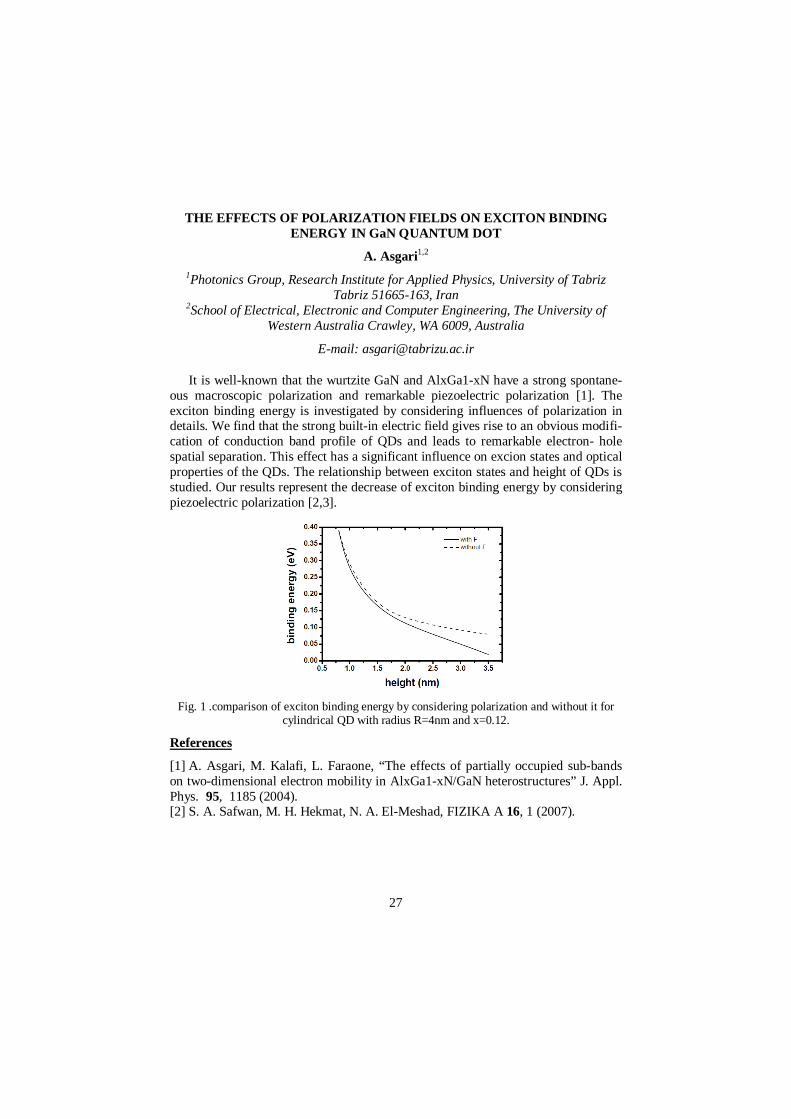
It is well-known that the wurtzite GaN and AlxGa1-xN have a strong spontane-ous macroscopic polarization and remarkable piezoelectric polarization [1]. The exciton binding energy is investigated by considering influences of polarization in details. We find that the strong built-in electric field gives rise to an obvious modifi-cation of conduction band profile of QDs and leads to remarkable electron- hole spatial separation. This effect has a significant influence on excion states and optical properties of the QDs. The relationship between exciton states and height of QDs is studied. Our results represent the decrease of exciton binding energy by considering piezoelectric polarization [2,3].
Fig. 1 .comparison of exciton binding energy by considering polarization and without it for cylindrical QD with radius R=4nm and x=0.12.
References
[1] A. Asgari, M. Kalafi, L. Faraone, “The effects of partially occupied sub-bands on two-dimensional electron mobility in AlxGa1-xN/GaN heterostructures” J. Appl. Phys. 95, 1185 (2004). [2] S. A. Safwan, M. H. Hekmat, N. A. El-Meshad, FIZIKA A 16, 1 (2007).
28
THE SCATTERING OF HOT ELECTRONS BY PHONONS IN AlGaN/ GaN QUANTUM DOT
A. Asgari1,2
1Photonics Group, Research Institute for Applied Physics, University of Tabriz Tabriz 51665-163, Iran
2School of Electrical, Electronic and Computer Engineering, The University of Western Australia Crawley, WA 6009, Australia
E-mail: [email protected]
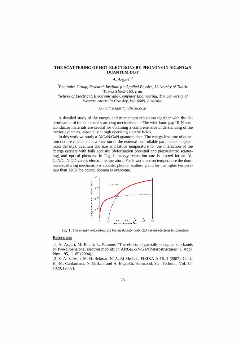
A detailed study of the energy and momentum relaxation together with the de-termination of the dominant scattering mechanisms in The wide band gap III-N sem-iconductor materials are crucial for obtaining a comprehensive understanding of the carrier dynamics, especially at high operating electric fields.
In this work we study a AlGaN/GaN quantum dots. The energy loss rate of quan-tum dot are calculated as a function of the external controllable parameters ns (elec-trons density), quantum dot size and lattice temperature for the interaction of the charge carriers with bulk acoustic (deformation potential and piezoelectric scatter-ing) and optical phonons. In Fig. 1, energy relaxation rate is plotted for an Al-GaN/GaN QD versus electron temperature. For lower electron temperature the dom-inant scattering mechanism is acoustic phonon scattering and for the higher tempera-ture than 120K the optical phonon is overcome.
Fig. 1 .The energy relaxation rate for an AlGaN/GaN QD versus electron temperature.
References
[1] A. Asgari, M. Kalafi, L. Faraone, “The effects of partially occupied sub-bands on two-dimensional electron mobility in AlxGa1-xN/GaN heterostructures” J. Appl. Phys. 95, 1185 (2004). [2] S. A. Safwan, M. H. Hekmat, N. A. El-Meshad, FIZIKA A 16, 1 (2007). Celik, H., M. Cankurtana, N. Balkan, and A. Bayrakli, Semicond. Sci. Technol., Vol. 17, 1829, (2002).
29
INFLUENCE OF SECOND HARMONIC ON STABILITY OF MAGNET IC FLUX IN LJJ, DESCRIBED BY DOUBLE SINE-GORDON EQUATIO N
P. Kh. Atanasova1, T. L. Boyadjiev2, E. V. Zemlyanaya1, and Yu. M. Shukrinov2
1LIT, JINR, 141980 Dubna, Moscow Region, Russia 2BLTP, JINR, 141980 Dubna, Moscow Region, Russia
E-mail: [email protected]
Physical properties of magnetic flux in Josephson junctions are the base of the modern superconducting electronics. Tunnel superconductor-insulator-superconductor (SIS) Josephson junctions have sinusoidal current phase relation, while with the decrease of the barrier transparency deviations from this relation take
place [1] and Josephson current ϕ+ϕ ∑∞mIII mmcS sinsin=
2=. The sign of the
second harmonic is important for many applications, in particular in junctions like SNINS and SFIFS, where N is a normal metal and F is a weak metallic ferromagnet [2].
In this work the static magnetic flux distributions in long Josephson junctions are investigated numerically, solving the boundary problem ,);(0,=2sinsin 21 llxaa'' −∈γ−ϕ+ϕ+ϕ− (1)
.=)( ehl' ±ϕ (2)
Here eh is the external magnetic field, γ is the external current and amplitudes
1a and 2a corresponds to cI and 2I in Fourier decomposition of Josephson current. The dependence on parameters of model is investigated. Stability of the static solutions is investigated by checking the sign of the smallest eigenvalue of the associated Sturm-Liouville problem. At each step of numerical calculation, the corresponding nonlinear boundary problem is solved on the basis of the continuous analog of Newton's method with the 4th order Numerov discretization scheme.
New solutions which do not exist in the traditional model, have been found. Investigation of the influence of second harmonic on stability of magnetic flux distributions for main solutions is performed.
References
[1] A.A. Golubov, M.Yu. Kypriyanov, The current-phase relation in Josephson junctions. Rev. Mod. Phys., 76, pp. 411 (2004) [2] V. V. Ryazanov, V. A. Oboznov, A. Yu. Rusanov et al., Coupling of Two Superconductors through a Ferromagnet: Evidence for a π Junction. Phys. Rev. Lett., 36, pp. 2427 (2001)
30
MAGNETIC FIELD AND PARTICLE CONCENTRATION COMPETITI VE EFFECTS ON FERROFLUID BASED ELASTOMER MICROSTRUCTUR E
M. Balasoiu1,2, I. Bica3, Yu.L. Raikher4, V.T. Lebedev5, A.V. Rogachev2, L. Almasy6, J. Kohlbreher6, N.S. Perov7, E.B. Dokukin2, and A.I. Kuklin 2
1National Institute of Physics and Nuclear Engineering, Bucharest, Romania 2Joint Institute of Nuclear Research, Dubna, Russia
3West University of Timisoara, Department of Electricity and Magnetism, Timisoara, Romania
4Institute of Continuum Media Mechanics, Ural Branch of RAS, Perm, Russia 5Petersburg Nuclear Physics Institute, Gatchina, Russia
6Paul Sherrer Institute, Villigen, Switzerland 7Moscow State University
E-mail: [email protected]
Magnetic elastomers belong to a specific class of so-called smart materials, due to their capabilities to respond to changes in their environment. They are composed of magnetic particles and a low-permeability matrix. Under an external magnetic field, a structure will form inside the material, or a structure embedded in the mate-rial will change. The magneto-elastic properties of composites are not only the sum of the elasticity of the polymer and the stiffness and magnetic properties of the filler, but also the result of a complex synergy of several effects, relevant at different length scales and detectable by different techniques.
Many studies of the observed reinforcing effect of magnetic fillers have ap-proached the problem from a magneto-mechanical point of view, and investigated the microscopic properties through study of the magneto-elastic responses of the composite [1]. Less well understood, however, are the effects of the interactions between the filler and the filler and surrounding polymer on submicroscopic length scales. Such length scales are ideally suited for small angle scattering investigations [2-5].
In the present paper, results on small angle neutron and X-ray scattering and magnetization investigations on the microstructure of ferrofluid based silicone-rubber elastomer samples are presented and analysed.
References
[1] G.V.Stepanov, D.Yu.Borin, Yu.L.Raikher et al., J.Phys.:Condens.Matter 20 (2008) 204121-6 [2] Y.Rharbi, B.Cabane, A.Vacher et al., Europhysics Letters 46 (4) (1999) 472-478 [3] A.Botti, W.Pyckhout-Hintzen, D.Richter et al., Polymer 44 (2003) 7505-7512 [4] S.Sen, Y.Xie, S.K.Kumar et al., Physical Review Letters 98, (2007) 128302-4 [5] M. Balasoiu, M.L. Craus, E.M. Anitas et al., Physics of Solid State 52 (2010) 861-865.
31
RELAXATION PROCESSES IN DOPED SILICON NANOCRYSTALS
V.A. Belyakov, A.A. Konakov, N.V. Kurova, and V.A. Burdov
University of Nizhniy Novgorod, Russia. 603950, Nizhniy Novgorod, Gagarin ave.23
E-mail: [email protected]
Incorporation of various silicon-based structures in optoelectronics is an actual problem up to now. Because of indirect band gap of silicon, light emission turns out to be suppressed or completely forbidden in such structures. As a means to improve the emittance of silicon crystallites, their doping with phosphorus was proposed. It has been shown experimentally that doping with phosphorus can several times in-crease photoluminescence intensity at certain conditions [1]. Theoretical estimations [2] show an increase of radiative recombination rate by 1 – 3 orders of magnitude depending on the phosphorus concentration.
However, not only radiative transitions, but also some nonradiative processes strongly influence the photon generation efficiency in Si nanocrystals. The goal of the present work is to examine the effect of doping on the nonradiative processes.
One of these processes is Auger recombination having in undoped nanocrystals the rate about 1 – 4 orders of magnitude higher [3] than the rate of the radiative tran-sitions. We have found that in doped nanocrystals, the rate of Auger recombination increases with increasing phosphorus concentration, but slower than the radiative recombination rate.
There are as well in Si quantum dots some relaxation processes being typical for ensembles of nanocrystals. Nanocrystals in an ensemble “interact” with each other, through, e.g., migration of excited carriers, or exciton transfer. We have calculated the rate of the carrier migration in an ensemble of doped Si crystallites, and found out that the rate sharply drops when the donor concentration achieves some critical value. This substantially enhances the radiative channel efficiency, and the quantum yield in whole.
References
[1] M. Fujii, A. Mimura, S. Hayashi, Y. Yamamoto, K. Murakami Hyperfine structure of the electron spin resonance of P-doped Si nanocrystals. Phys. Rev. Lett. 89, 206805 (2002) [2] V.A. Belyakov, V.A. Burdov - XΓ mixing in P-doped Si Nanocrystals: Im-provement of the photon generation efficiency. Phys. Rev. B 79, 035302 (2009) [3] M. Lannoo, C. Delerue and G. Allan Theory of radiative and nonradiative transitions for semiconductor nanocrystals. J. Lumin. 70, 170 (1996)
32
NANOCONES ROLLING IN HYDRO-THERMAL MEDIUM AND FLOWS IN CONICAL DOMAINS
I.V.Blinova, K.N.Kiz’yurova, and I.Yu.Popov
St.-Petersburg State University of Information Technologies, Mechanics and Optics Kronverkskii, 49, St.-Petersburg, 197101, Russia
E-mail: [email protected], Web page: www.ifmo.ru
In many applications of tubular nanostructures it is necessary to describe fluid flows through these systems, which have many specific features. Moreover, these flows play an important role in the processes of nanotubes formation. Our report is devoted to the description of these processes in conical nanostructures. Hydro-thermal method of nanotube formation is very effective [1]. But it is often led to formation of nanostructures of different morphology, particularly, nanocones. Pro-cess of nanocone formation due to rolling from plane structure in hydro-thermal medium is considered. The system comes to equilibrium if there is lattices corre-spondence between neighbor layers. Due to this reason the conical angle depends on the lattice parameters. This dependence is analyzed. Movement of the conical sur-face during the formation process leads to the appearance of flow in conical domain which has an influence on the formation process. The picture of the streamlines for the flow is obtained. The influence of the flow on the speed of the formation process and on the type of obtained nanostructure is described.
References
[1] S.A. Chivilikhin, I.Yu. Popov, V.V. Gusarov Dynamics of nanotube rolling in viscous fluid. Doclady RAS, 412 (2), 201-203 (2007)
33
SURFACE PLASMON-POLARITONS IN GRAPHENE LAYER: DISPE R-SION RELATION AND EXCITATION BY ATTENUATED TOTAL IN TER-
NAL REFLECTION METHOD
Yu.V. Bludov, N. M. R. Peres, and M. I. Vasilevskiy
Centre of Physics, University of Minho, Campus de Gualtar, 4710-057, Braga, Portugal
E-mail:[email protected]
In the paper we consider theoretically surface plasmon-polaritons (SPPs) in sin-gle graphene layer, surrounded by two semi-infinite dielectric media. The SPP dis-persion relation was obtained in the self-sustaining way using the expression for the graphene conductivity, obtained earlier in [1]. It is shown, that the peculiarity of SPP dispersion relation in graphene (compared to the usual 2D electron system) is the existence of SPP at frequencies less than some critical frequency, whose value is approximately proportional to the chemical potential of graphene. Dealing with problem of SPP excitation, the possibility to excite the SPP in single graphene layer in the long-wavelength range using the attenuated total internal reflection method is shown. We demonstrate that in the case of graphene the parameters of the SPP exci-tation (like frequency, reflectivity of attenuated total internal reflection scheme) can be tuned by applying the gate voltage to the graphene layer.
References
[1] T. Stauber, N. M. R. Peres, and A. K. Geim, PRB 78, 085432 (2008)
34
VERTICALLY ALIGNED CARBON NANOTUBES FOR MEAS APPLIC A-TIONS
J.R. Castro Smirnov
Universitat de Barcelona, Calle Palermo # 2, 2-3, 08019, Barcelona, Spain
E-mail: [email protected]
In this proposal, a methodology to fabricate carbon nanotube based electrodes using plasma enhanced chemical vapour deposition will be defined. The final inte-grated microelectrode based devices should present specific properties that make them suitable for microelectrode arrays applications. The methodology studied should enable the construction of highly regular and dense vertically aligned carbon nanotube (VACNT) forests that can be confined within the patterned bounds of a desired surface.
35
LOCAL FRANCK-CONDON FACTORS IN SUSPENDED CARBON NANOTUBE QUANTUM DOTS
F. Cavaliere1, E. Mariani2, R. Leturcq3,4, C. Stampfer3,5, and M. Sassetti1
1 LAMIA CNR, DIFI, Universitа di Genova, Via Dodecaneso 33, 16146 Genova, Italy
2 Institut fьr Theoretische Physik, Freie Universitдt Berlin, Arnimallee 14, 14195 Berlin, Germany
3 Laboratory for Solid State Physics, ETH Zurich, 8093 Zurich, Switzerland 4 IEMN CNRS-UMR 8520, ISEN, Avenue Poincarй, BP 60069, 59652
Villeneuve d'Ascq Cedex, France 5 JARA-FIT and II. Institute of Physics, RWTH Aachen University, 52074
Aachen, Germany
E-mail: [email protected]
When electrons tunnel through a quantum dot embedded into a suspended carbon nanotube (CNT), quantized vibrational modes (vibrons) can be excited [1,2]. In such systems, vibrons couple both to the total dot charge and to electron density fluctuations. For the description of such systems however the Anderson-Holstein (AH) model, in which the vibron couples only to the total charge, is usually employed. The AH model yields position-independent Franck-Condon (FC) factors - giving rise to the FC blockade phenomenon [3] which has been confirmed in a recent experiment [2].
In this work [4] it will be shown that the effects of density fluctuations are indeed crucial when the size and location of the dot and of the vibron do not coincide. For a vibron smaller than the quantum dot local FC factors, with a strong dependence on position, arise - in sharp contrast with the predictions of the AH model. This has profound consequences on the transport properties of the system. With our theory we are able to explain a peculiar suppression of conductance traces observed in recent experiments [2] in terms of position-dependent FC factors.
References
[1] S. Sapmaz et al., Tunneling in Suspended Carbon Nanotubes Assisted by Longitudinal Phonons, Phys. Rev. Lett. 96, 026801 (2006). [2] R. Leturcq et al., Franck-Condon blockade in suspended carbon nanotube quantum dots, Nature Phys. 5, 327 (2009). [3] J. Koch et al., Franck-Condon Blockade and Giant Fano Factors in Transport through Single Molecules, Phys. Rev. Lett. 94, 206804 (2005). [4] F. Cavaliere et al., Asymmetric Franck-Condon factors in suspended carbon nanotube quantum dots, arXiv:0911.2122 (2009).
36
HIGH PRESSURE PHASE TRANSITION OF NOVEL MATERIALS
R. Chauhan
Barkatullah university,Bhopal(M.P.), 30, Prakash Nagar,Gyan Jyoti Public School, Ayodhya ByPass Road, Bhopal(M.P.), 462001, Bhopal, India
E-mail: [email protected]
We have carried out high pressure theoretical structural studies of yittrium ni-tride YN to examine the phase transition phenomena from the NaCl structure to CsCl structure by using a three body potential model (TBPM). The phase transition pressure (140 GPa) predicted by this approach is close to the phase transition pres-sure, predicted by others (138 GPa). YN is a novel and less explored material. Under high pressure YN goes through a sudden collapse in volume showing the first order phase transition. To understand the effect of pressure we studied bulk properties, elastic constants and their combination. The pressure volume equation of state (EOS) provides meaningful signatures of physical and chemical phenomena under high pressure. Moreover we have successfully checked the stability criterion for this compound.
37
NANOSTRUCTURES BASED ON HYDROGEN-FUNCTIONALIZED GRA -PHENES AS MATERIALS FOR APPLICATIONS IN NANODEVICES
L.A. Chernozatonskii
Emanuel Institute of Biochemical Physics of RAS, Moscow, 119334, Russia
1. Introduction (pour graphene sheets and graphene nanoribbons [1], , graphane [2], diamane [3]) 2. New structures based on graphene, graphane and diamane and their electronic and mechanical properties.
2.1. Quasi- two-dimensional superlattices and electronic waveguids based on graphene lined by chemically bounded hydrogen atom lines or nanopeaces [4-7]. Transactions of semimetal-semiconductor-dielectric phases X-, T- and Y-types of graphene structures.
2.2. "Quasi 1D" superlattices and quantum dots based on graphene ribbons lined by chemically bounded hydrogen atoms.
2.3. Atomic structure, elastic and electronic properties of diamanes based on chemically bound graphene layers covered by hydrogen on both sides and bi-graphane - diamane nanostructures.
3. The possible applications of described structures in nanoelectronics (nanowires, transistors, switchers, rectificators), as sensors, as mechanical elements (vibrators, springs, membranes, cantilever diamane tips) and optical elements. The work was supported by RFBR grant 08-02-01096 and RAS program 21.
References
[1] K.S. Novoselov, A.K. Geim, S.V. Morozov, et al. Science 306, 666 (2004) [2] D.C. Elias, R.R. Nair, T.M.G. Mohiuddin, et al. Science 324, 236 (2009) [3] L.A. Chernozatonskii, P.B. Sorokin, A.G. Kvashnin, D.G. Kvashnin. JETP Let-ters 90, 144 (2009) [4] L.A. Chernozatonskii, P.B. Sorokin, J. Brüning. Appl. Phys. Lett. 91, 183103 (2007) [5] A. K. Singh and B. I. Yakobson, Nano Lett. 9, 1540, (2009) [6] M.Z. Flores et al. Nanotechnology 20, 465704 (2009) [7] L.A. Chernozatonskii, P.B. Sorokin. J. Phys. Chem. C (2010) (in press).
38
THE SCATTERING FROM GENERALIZED CANTOR FRACTALS
A.Yu. Cherny1, E.M. Anitas1,2, A.I. Kuklin 1, M. Balasoiu1,2, and V.A. Osipov1
1 Joint Institute for Nuclear Research, Dubna 141980, Russia 2 Horia Hulubei National Institute of Physics and Nuclear Engineering, RO-
077125 Bucharest-Magurele, Romania
E-mail: [email protected]
We suggest a three dimensional generalization of well-known triadic Cantor fractal in one dimension. Its fractal dimension is controlled with a cut-off parameter and can vary from 0 to 3. The intensity profile of a small-angle scattering from the generalized Cantor fractals is calculated. The considered system is generated by a set of iterative rules, each iteration corresponds to a certain fractal generation. A small-angle scattering is considered from the monodispersive sets being randomly oriented and placed. The scattering intensities represent minima and maxima superimposed on a power law decay with the exponent being equal to the fractal dimension of the scatterer, but the minima and maxima are damped with increasing polydispersity of the fractal sets. It is shown that for a finite generation of the fractals, the exponent value changes at sufficiently large wave vectors from the fraction dimension to 4, the value given by the usual Porod law. It is shown that the number of particles, from which the fractal is composed, can be estimated from the value of the boundary between the fractal and Porod region. The radius of gyration of the fractal is calculated analytically.
References
[1] P.W. Schmidt and X. Dacai, Calculation of the small-angle x-ray and neutron scattering from nonrandom (regular) fractals, Phys. Rev. A, 33, 560 (1985) [2] H. Mayama and K. Tsuji, Menger sponge-like fractal body created by a novel template method, J. Chem. Phys., 125, 124706 (2006) [3] G. R. Newkome, P. Wang, C. N. Moorefield, T. J. Cho, P. P. Mohapatra, S. Li, S.-H. Hwang, O. Lukoyanova, et al., Nanoassembly of a Fractal Polymer: A Molecular "Sierpinski Hexagonal Gasket", Science, 312, 1782 (2006). [4] G. F. Cerofolini, D. Narducci, P. Amato and E. Romano, Fractal Nanotechnology, Nanoscale Res. Lett., 3, 381 (2008) [5] Yu. Cherny, E. M. Anitas, A. I. Kuklin, M. Balasoiu, V. A. Osipov, The scattering from generalized Cantor fractals, http://arxiv.org/abs/0911.2497v1 (2009)
39
AN ORBITAL ENTANGLEMENT IN TWO--ELECTRON QUANTUM DO TS IN A MAGNETIC FIELD
A.V. Chizhov1 and R.G. Nazmitdinov1,2
1Bogoliubov Laboratory of Theoretical Physics, JINR, Dubna, Russia 2 Departament de Fsica, Universitat de les Illes Balears Palma de Mallorca, Spain
Nowadays there is an enormous experimental and theoretical activity focussed on the study of properties of few--electron quantum dots (QDs). One of the main motivations is due to a rapid development of the field of quantum computing, since the entangled states of the electrons confined in a QD may give a natural realization of a quantum bit or ``qubit" [1]. It is also expected that QDs could lead to novel device applications in quantum cryptography and information storage. However, the measure of entanglement which is one of the most subtle and intriguing phenomena in nature is still debatable [2].
Recently we developed an analytical approach to study the degree of entanglement in a model of two--coupled harmonic oscillators [3]. Note, that in condensed matter physics this model is used as a starting point for analysis of electronic properties of QDs in a perpendicular magnetic field [4]. Based on this fact, we have performed a detailed study of the shape of two--electron QD on the degree of the orbital entanglement. We assume that noninteracting electrons move in a two--dimensional parabolic confining potential under the perpendicular magnetic field. We found that a closed circular QD does not reveal an orbital entanglement of electrons. The increase of the shape deformation leads to increase of the degree of the entanglement. The magnetic field increases the entanglement as well. However, in the latter case there is a saturation effect: for each deformed shape there is an asymptotic value of the entanglement. Introducing the coupling between the two-electron QD and the environment (the thermo--bath), we study also the effect of dissipation on the degree of the entanglement.
References
[1] R. Hanson, L. P. Kouwenhoven, J. R. Petta, S. Tarucha, and L. M. K. Vander-sypen, Spins in few--electron quantum dots Rev. Mod. Phys, Vol. 79, 1217 (2007). [2] L. Amico, R. Fazio, A. Osterloh, and V. Vedral, Entanglement in many--body systems Rev. Mod. Phys, Vol. 80, 517 (2008). [3] A. V. Chizhov and R. G. Nazmitdinov, Entanglement control in coupled two--mode boson systems Phys. Rev. A, Vol. 78, 0641302 (2008). [4] R. G. Nazmitdinov, Magnetic field and symmetry effects in small quantum dots Fiz. Elem. Chastits At. Yadra, Vol. 40, 144 (2009) [ Physics of Particles and Nuclei Vol. 40, 71 (2009)].
40
REALISTIC CONFINEMENT POTENTIAL FOR A SQUARE PATTER NED TWO-DIMENSIONAL SEMICONDUCTOR QUANTUM DOT AND ITS AP -
PROXIMATED CIRCULAR COUNTERPART
O. Ciftja
Department of Physics, Prairie View A&M University, Prairie View, Texas 77446, USA
E-mail: [email protected]
Two-dimensional semiconductor quantum dot systems are typical nanoscale structures in which a few number of electrons is confined in a small region of space by applying external electric gate potentials. While the detailed form of the confin-ing potential depends on the specific experimental setup, the parabolic confinement model has commonly been used because of its simplicity. Clearly, on those instances in which the experimental setup involves placement of gate potentials with sharp geometric features, the area depleted of electrons, thus the quantum dot region can-not be considered circular. If, for simplicity, we consider the confinement region of the electrons as square in shape, then an accurate calculation of the properties of such square patterned quantum dot should be made by using a realistic confinement potential originating from that particular configuration. We calculated exactly such a confinement potential for a square quantum dot. The particular analytic form of this realistic potential is complicated given the dependence on the two-dimensional posi-tion coordinates, rather than simply the distance from the center of the quantum dot. In this work we choose to substitute the realistic confinement potential for a square patterned quantum dot with an approximated circular symmetric potential. We as-sess the quality of this approximation and discuss instances in which one can relia-bly use the approximated simplified potential instead of the computationally un-yielding exact one.
41
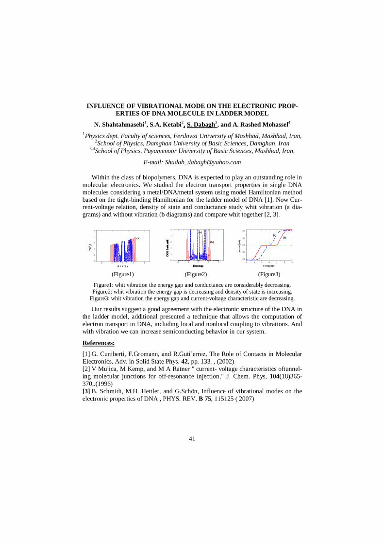
INFLUENCE OF VIBRATIONAL MODE ON THE ELECTRONIC PRO P-ERTIES OF DNA MOLECULE IN LADDER MODEL
N. Shahtahmasebi1, S.A. Ketabi2, S. Dabagh3, and A. Rashed Mohassel4 1Physics dept. Faculty of sciences, Ferdowsi University of Mashhad, Mashhad, Iran,
2School of Physics, Damghan University of Basic Sciences, Damghan, Iran 3,4School of Physics, Payamenoor University of Basic Sciences, Mashhad, Iran,
E-mail: [email protected]
Within the class of biopolymers, DNA is expected to play an outstanding role in molecular electronics. We studied the electron transport properties in single DNA molecules considering a metal/DNA/metal system using model Hamiltonian method based on the tight-binding Hamiltonian for the ladder model of DNA [1]. Now Cur-rent-voltage relation, density of state and conductance study whit vibration (a dia-grams) and without vibration (b diagrams) and compare whit together [2, 3].
-2 - 1 0 1 2- 5
- 4
- 3
- 2
- 1
0
( b )( a )
log
(TE)
E n e r g y
- 2 - 1 0 1 20
1
2
3
4
5
( b )
( a )
-3 -2 -1 0 1 2 3
-0.2
-0.1
0.0
0.1
0.2
(b)(a)
curr
ent(
nA
)
voltage(v)
(Figure1) (Figure2) (Figure3)
Figure1: whit vibration the energy gap and conductance are considerably decreasing. Figure2: whit vibration the energy gap is decreasing and density of state is increasing.
Figure3: whit vibration the energy gap and current-voltage characteristic are decreasing.
Our results suggest a good agreement with the electronic structure of the DNA in the ladder model, additional presented a technique that allows the computation of electron transport in DNA, including local and nonlocal coupling to vibrations. And with vibration we can increase semiconducting behavior in our system.
References:
[1] G. Cuniberti, F.Gromann, and R.Guti´errez. The Role of Contacts in Molecular Electronics, Adv. in Solid State Phys. 42, pp. 133. , (2002) [2] V Mujica, M Kemp, and M A Ratner " current- voltage characteristics oftunnel-ing molecular junctions for off-resonance injection," J. Chem. Phys, 104(18)365-370,.(1996) [3] B. Schmidt, M.H. Hettler, and G.Schön, Influence of vibrational modes on the electronic properties of DNA , PHYS. REV. B 75, 115125 ( 2007)
42
ENERGY SPECTRUM OF DIRAC ELECTRONS IN GRAPHENE QUANTUM DOTS
M. Dineykhan, S. A. Zhaugasheva, and Zh. Bisarieva
Bogoliubov Laboratory of Theoretical Physics, JINR, Dubna al-Farabi Kazak National University, Almaty, Kazakhstan
We investigate the massless chiral fermions confined in a graphitic parabolic quantum dot. Recently, single layers carbon atoms (graphene) have been obtained experimentally [1]. The spectrum of excitations in graphene is described by a two-dimensional analog of the relativistic Dirac equation [2,3]. The Hamiltonian of a single electron in graphene with confinement potential is ( ) , )(= xVppcH yyxx +σ+σ (1)
where c ≈ 108 cm/s is the Fermi velocity and ∇−
ip = , and σ are the Pauli matrices. The parabolic potential represented as
.2)( 02 xUxxV = (2)
In the nonrelativistic limits the Dirac Hamiltonian is given by the effective Hamiltonian [2]
, )(= 22 xVppcH yxeff ++ (3)
This effective Hamiltonian can bee represented as
, )(2
1
2=)( 2
22
xVcpp
Hyx
eff +µ+µ+
µ (4)
where µ is the variational parameter. Let as determine the energy spectrum of the effective Hamiltonian from the SE . ))(=)()( xxH Neff ΨεΨµ (5)
The energy spectrum εN with N th resonance represented as (for details see [4])
, 3
12
3=
2
22
ζ
+ζ
ε
yN
NN
pc (6)
where used the notation
( ). )(1= 20 nUcxN +ζ (7)
For a given value of the transverse momentum py ≠ 0 and in the case cpy << εN, we can determine the probability of tunneling between the boundet and unboundet states.
References [1] K.S. Novoselov it et al., Science 306,p.666(2007). [2] P.G.Silvestrov, K.B.Efetov, Phys. Rev. Lett., 98, p.0168021232(1951). [3] H.Y.Chen,V.Apalkov, T.Chakraborty, Phys. Rev. Lett. 98, p.186803(2007). [4] M.Dineykhan, S.A. Zhaugasheva, N.Sh. Toinbaeva, J. Phys.B:At. Mol. Opt. Phys., 43, p.015003(2010).
43
PLASMA OSCILLATIONS AND ELECTRON-ELECTRON INTERAC-TIONS IN 2D ELECTRON SYSTEMS
A.B. Dubois
Ryazan State Radio Technical University, Gagarin, 59/2, 390005, Ryazan, Russia Ryazan Institute of Open Education, Bronnaya, 2, 390010, Ryazan, Russia
E-mail: [email protected]
Electron-electron interactions in a single highly doped heterojunction Al xGa1-x/GaAs are considered taking both intra- and intersubband transitions. Char-acteristic features of 2D electron systems, such as the amplitude-frequency modula-tion, beatings and sharp bends in the oscillation amplitude magnetic field depend-ence make the description of Landau quantization damping in terms of the Dingle temperature rather problematic [1]. Another point to be pointed out is the fact that in the magnetic field range where a strong amplitude-frequency modulation take place the perturbed – subband electrons are in the state closed to the quantum limit and one can speak of the oscillations period in a rather limited sense.
References
[1] V.I. Kadushkin, A.B. Dubois ”Bottleneck” in Electron-Electron Interactions and Anomalies in the Landau Quantization Damping Phys. Low-Dim. Struct., 7/8, 7-24 (2003)
44
THE EMISSION DIFFERENTIAL CROSS SECTION OF AN ELECT RON IN THE SEMIPARABOLIC QUANTUM WELL
P. Elahi1, A. Keshavarz1, and M. Mehdipour2
1Physics Department, Shiraz University of Technology, Shiraz, Iran 2Azad University, Fars Science and Research Branch, Iran
Email: [email protected]
An electron in an asymmetrical semiparabolic quantum well has been considered for a typical AsGaAl/GaAs 1 xx − material. After calculation the electron state, the material has been exposed to a time-dependent electromagnetic field. By using the time-dependent perturbation theory and using dipole moment approximation, the electron emission probability rate has been calculated and then the emission differ-ential cross section has been derived by using the following relation:
32 2ˆ( )( )
2 2 3
4 ˆ(2 )
fi c nf
mk Lde i
d mω ⋅σ π α= ε ⋅
Ω ω π
xK p
Where i and fK are initial electron ket in semiparabolic quantum well and free
electron ket, respectively. The obtained relations, then used for AsGaAl/GaAs 1 xx − material and discussed.
References
[1] I. Karabulut, H. Safak, M. Tomal, Nonlinear optical rectification in asymmet-rical semiparabolic quantum wells, Solid State Communications, 135, 735-738(2005) [2] J J Sakurai, Modern Quantum Mechanics, Addison-Wisely Publishing Company, (1994)
45
THE PHOTOELECTRIC DIFFERENTIAL CROSS SECTION FOR A QUANTUM BOX WITH FINITE CONFINING
P. Elahi1, M. Hooshmand2
1Physics Department, Shiraz University of Technology, Shiraz, Iran Email: [email protected]
2Physics Department, Shiraz Payame Noor University, Shiraz, Iran
The differential cross section for photoelectric effect for a quantum box with fi-nite confining potential has been investigated in this paper. The semi classical ap-proach has been used and the photon electromagnetic radiation has been considered as a time-dependent perturbation term for the initial electron in the quantum box with finite confining potential. The obtained results then have been used for
AsGaAl/GaAs 1 xx − and the differential cross section has been plotted versus θ in
spherical coordinate system and discussed. The results show the maximum of the cross section at 0θ = and decreasing toward to π/2.
References
[1] S. Unlu, I. Karabulut and H. Safsk, Linear and nonlinear intersubband optical absorption coefficients and refractive index changes in a quantum box with finite confining potential, Physica E , 33 319-324 (2006) [2] J J Sakurai, Modern Quantum Mechanics, Addison-Wisely Publishing Company, (1994)
46
SPIN TRANSPORT THROUGH A TRIANGULAR GRAPHENE FLAKE
R. Farghadan1, A. Saffarzadeh2,3, E. Saievar Iranizad1
1Department of Physics, Tarbiat Modares University, Tehran, Iran, 2Department of Physics, Payame Noor University, Tehran, Iran,
3Department of Nano-Science, Institute for Research in Fundamental Sciences (IPM), Tehran, Iran
E-mail: [email protected]
We theoretically investigate the coherent spin polarized transport through a gra-phene flake by focusing on the magnetic effect of the zigzag edges [1, 2 and 3]. The graphene flake with triangular shape is sandwiched between two nonmagnetic one dimensional electrodes. The semi-infinite electrodes cannot effectively alter the fer-romagnetic spin configuration at the zigzag edges. The electronic structure and magnetic properties of this junction are simulated self consistently by use of the sin-gle-band tight-binding approximation and the mean-field Hubbard model [2, 4]. Also, using the non-equilibrium Green’s function technique and the Landaure-Buttiker theory [5] the spin density of states, the spin-polarized currents and the magnetoresistance are calculated.
Our numerical results show that the spin transport strongly depends on the mag-netic configuration of the graphene flake and hence, a fully spin-polarized conduct-ance without external field can be produced. In addition, the current-voltage charac-teristic shows a high splitting between spin up and spin down currents due to the effect of edge-induced magnetism on the electronic transport through the junction. The results may be useful for carbon-based spintronic applications.
References
[1] E.H. Lieb Two Theorems on the Hubbard Model. Phys. Rev. Lett. 62, 1201 (1989) [2] M. Fujita, K. Wakabayashi and K. Nakada Peculiar Localized State at Zigzag Graphite Edge. J. Physical Society of Japon, 65, 1920 (1996) [3] J.F. Rossier and J. J. Palacios Magnetism in Graphene Nanoislands. Phys. Rev. Lett. 99, 177204 (2007) [4] M.P.L. Sancho, F.d. Juan and M.A.H. Vozmediano Magnetic moments in the presence of topological defects in graphene. Phys. Rev. B, 79, 075413 (2009) [5] S. Datta, Quantum Transport atom to transistor. Cambridge University Press, 2rd edition (2006)
47
MODELING OF FIELD EMISSION FROM GRAPHENE
V.A. Fedirko1,2, S.V. Polyakov2, V.V. Vyurkov 3 and D.A. Zenyuk1
1MSUT “Stankin”, Vadkovski Alley 1, 127994 Moscow, Russia 2IMM RAS, Miusskaya Square 4a, 125047, Moscow, Russia 3IPT RAS, Nakhimov Avenue 36/1, 117218, Moscow, Russia
E-mail: [email protected], [email protected]
We report on modeling of electron field emission from an edge of a graphene layer. It is well-known that carbon nanotubes can serve as affective cold emitters[1]. That motivated us to make an attempt to study that effect in graphene.
It was shown [2] that strong electron – hole scattering dominates in graphene. For that reason we use a hydrodynamic model with self-consistent electric field for charge transport in a graphene layer [3]. The set of equations is added with proper boundary conditions. Tunneling current is used as a boundary condition for dynamic equations at the free edge of graphene. The simplified approach has been used for calculation of tunneling probability at that stage.
The problem has been treated numerically on the basis of the approaches devel-oped in [4,5]. Emission current has been calculated, taking in account non-homogeneous charge distribution near the emitting edge of graphene.
That study may also pave an approach to the problem of field emission from a carbon nanotube, which is not quite solved yet.
References
[1] A.V. Eletskii N.N., Physics-Uspekhi (Russian Advances in Physical Sciences), 172 (4), 401 (20O2) [2] V. Vyurkov,V. Ryzhii, Pis’ma v ZhETF, 88 (5), 370 (2008) [3] V. Vyurkov, I. Semenikhin, M. Ryzhii, T. Otsuji, and V. Ryzhii, Int. Symp. on Graphene Devices,. Nov.17-19, Aizu-Wakamatsu, Japan, Technical Digest, pp. 32-33 (2008) [4] S.V. Polyakov, V. F. Fedirko, in the Book of Abstracts of the Intern. Conf. on Mathematical modeling and computational physics – MMCP, Dubna, July 7-11, 157-158 (2009) [5] V.A. Fedirko, D. A. Zenyuk, S. V. Polyakov, in the Book of Abstracts of the Intern. Conf. on Mathematical modeling and computational physics – MMCP, Dub-na, July 7-11, 73 (2009)
48
QUANTUM FARADAY EFFECT AND CASIMIR INTERACTION AS N EW QFT TEST IN GRAPHENE
I. Fialkovsky1,2, D. Vassilevich2,3
1Instituto de Física, Universidade de São Paulo, Brazil 2Department of Theoretical Physics, St. Petersburg State University, Russia
3CMCC, Universidade Federal do ABC, Brazil
Relativistic Quantum field Theory (QFT) is known to be readily applicable to description of graphene optical and electronical properties. It is due to the fact that quasy-particles in graphene monolayer in the low-energy approximation are de-scribed by the relativistic quasi-massless Dirac equation. Purely QFT techniques can be employed to reconstruct the ac/dc conductivity of graphene monolayer which is given in this approach by the polarization operator – the one-loop correction to the photon propagator.
As was shown before [1], the presence of parity-odd terms in the polarization tensor (equivalently the none-zero off-diagonal part of the aс conductivity) leads to rotation of polarization of light passing through suspended graphene films. In exter-nal magnetic field, this would correspond to a quantum Faraday Effect. We show [3] that at low temperatures (or high B-fields) the angle of rotation exhibits clear Lan-dau quantization. The magnitude of the effect is up to 10-2 rad which is well above the sensitivity limits of modern optical instruments, thus giving opportunity to test the QFT predictions for graphene systems.
As another way to check relativistic field theory we propose the calculation of the Casimir interaction between suspended graphene monolayer and plane parallel ideal conductor [2]. The Casimir effect is defined by quantum vacuum fluctuations which are governed by the very same polarization operator. Apart of strong depends of the Casimir energy on the mas gap of quasi-particles we also reveal the influence of the non-vanishing density of carriers in the graphene (chemical potential) and the temperature [3]. The force is experimentally measurable though being rather weak.
References
[1] I.V. Fialkovsky, D.V. Vassilevitch, J. Phys. A: Math. Theor. 42 442001 (2009), arXiv: 0902.2570 [hep-th]. [2] M. Bordag, I. V. Fialkovsky, D. M. Gitman, D. V. Vassilevich, Phys. Rev. B 80 245406 (2009), arXiv:0907.3242 [hep-th]. [3] I.V. Fialkovsky, D.V. Vassilevitch, in preparation.
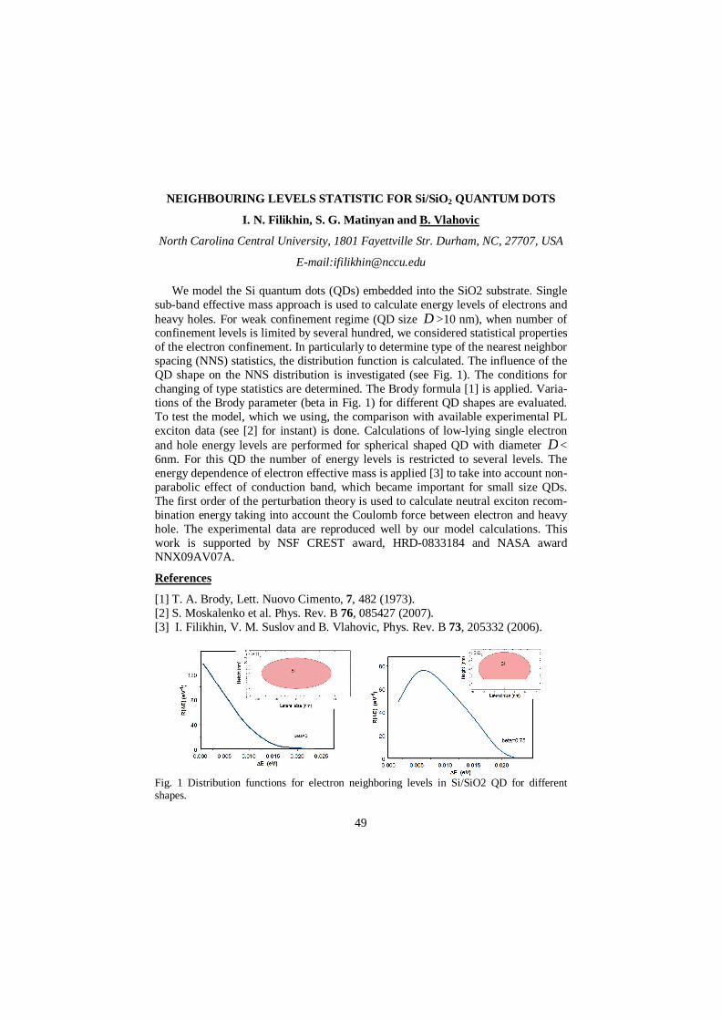
49
NEIGHBOURING LEVELS STATISTIC FOR Si/SiO 2 QUANTUM DOTS
I. N. Filikhin, S. G. Matinyan and B. Vlahovic
North Carolina Central University, 1801 Fayettville Str. Durham, NC, 27707, USA
E-mail:[email protected]
We model the Si quantum dots (QDs) embedded into the SiO2 substrate. Single sub-band effective mass approach is used to calculate energy levels of electrons and heavy holes. For weak confinement regime (QD size D >10 nm), when number of confinement levels is limited by several hundred, we considered statistical properties of the electron confinement. In particularly to determine type of the nearest neighbor spacing (NNS) statistics, the distribution function is calculated. The influence of the QD shape on the NNS distribution is investigated (see Fig. 1). The conditions for changing of type statistics are determined. The Brody formula [1] is applied. Varia-tions of the Brody parameter (beta in Fig. 1) for different QD shapes are evaluated. To test the model, which we using, the comparison with available experimental PL exciton data (see [2] for instant) is done. Calculations of low-lying single electron and hole energy levels are performed for spherical shaped QD with diameter D< 6nm. For this QD the number of energy levels is restricted to several levels. The energy dependence of electron effective mass is applied [3] to take into account non-parabolic effect of conduction band, which became important for small size QDs. The first order of the perturbation theory is used to calculate neutral exciton recom-bination energy taking into account the Coulomb force between electron and heavy hole. The experimental data are reproduced well by our model calculations. This work is supported by NSF CREST award, HRD-0833184 and NASA award NNX09AV07A.
References
[1] T. A. Brody, Lett. Nuovo Cimento, 7, 482 (1973). [2] S. Moskalenko et al. Phys. Rev. B 76, 085427 (2007). [3] I. Filikhin, V. M. Suslov and B. Vlahovic, Phys. Rev. B 73, 205332 (2006).
Fig. 1 Distribution functions for electron neighboring levels in Si/SiO2 QD for different shapes.
50
EFFECTIVE SPIN-FLIP SCATTERING IN DIFFUSIVE SUPERCONDUCTING PROXIMITY SYSTEMS WITH MAGNETIC
DISORDER
D.A. Ivanov1, Ya.V. Fominov2, M.A. Skvortsov2, and P.M. Ostrovsky2,3
Institute of Theoretical Physics, Ecole Polytechnique Fйdйrale de Lausanne (EPFL), CH-1015 Lausanne, Switzerland
L.D. Landau Institute for Theoretical Physics RAS, 142432 Chernogolovka, Moscow region, Russia
Institut fьr Nanotechnologie, Forschungszentrum Karlsruhe, 76021 Karlsruhe, Germany
E-mail: [email protected]
We revisit the problem of diffusive proximity systems involving superconductors and normal metals (or ferromagnets) with magnetic disorder. On the length scales much larger than its correlation length, the effect of sufficiently weak magnetic disorder may be incorporated as a local spin-flip term in the Usadel equations. We derive this spin-flip term in the general case of a three-dimensional disordered Zeeman-type field with an arbitrary correlation length. Three different regimes may be distinguished: pointlike impurities (the correlation length is shorter than the Fermi wavelength), medium-range disorder (the correlation length between the Fermi wavelength and the mean free path), and long-range disorder (the correlation length longer than the mean free path). We discuss the relations between these three regimes by using the three overlapping approaches: the Usadel equations, the non-linear sigma model, and the diagrammatic expansion. The expressions for the spin-flip rate agree with the existing results obtained in less general situations.
References
[1] D.A. Ivanov, Ya.V. Fominov, M.A. Skvortsov, and P.M. Ostrovsky, Effective spin-flip scattering in diffusive superconducting proximity systems with magnetic disorder. Phys. Rev. B, 80, 134501 (2009)
51
MoSI NANOWIRES: FROM A ONE-DIMENSIONAL QUANTUM FLUID TO SELF-ORGANISED CRITICAL NETWORKS
C. Gadermaier1, J. Strle1, M. Uplaznik1, D. Vengust1, B. Bercic1, and D. Mihailovic 1
1Deparment of Complex Matter, Jozef-Stefan Institute, Jamova 39, 1000 Ljubljana, Slovenia
E-mail: [email protected], Web page: http://complex.ijs.si/index.html
Progress in nanotechnology crucially depends on molecular-scale materials with tunable physical or functional properties, yet with well-defined and controllable ge-ometrical structure. Mo6S9-xIx (MoSI) nanowires (NWs) self-assemble into function-al networks and qualify for applications as diverse as lubricant additives, field emit-ters, battery electrodes, (bio)chemical sensors, and as conductive or reinforcing component of composites. They disperse in many common solvents including water, where they occur in bundles of diameters ranging from a few 100 nm down to single wires (below 1 nm).
Individual MoSI wires have extremely low coupling to the environment and to each other, which leads to extreme one-dimensional quantum electronic transport behaviour. Flexible bundles of MoSI NWs with different diameters reveal systemat-ic power-law dependence of the conductivity on temperature and voltage. This be-haviour can be most convincingly described by tunneling through Tomonaga-Luttinger liquid segments of MoSI wire, which is in some cases modified by envi-ronmental Coulomb blockade from deformations or imperfections of the MoSI wires.
Scale-free self-organized critical networks such as the human brain show re-sistance to failure, fast signal processing, and are of particular interest for nanoelec-tronics. Hybrid networks of MoSI wires and gold nanoparticles self-assemble in solution. While the length distribution of individual nanowires is log-normal, the lengths of the edges in the network deposited on a substrate show a strong power-law tail indicating scale invariance. This shows that the self-organized critical be-haviour is not a property of the nanowire synthesis, but of their self-assembly into networks.
52
A GENERAL THEORY OF SPIN-RELAXATION IN TWO-DIMENSION AL SEMICONDUCTORS
V. Galitski
Center for Nanophysics and Advanced Materials and Joint Quantum Institute, Uni-versity of Maryland, College Park, MD 20742-4111
In this talk, I will review our recent work on microscopic theory of spin relaxa-tion in two-dimensional semiconductors, which was recently verified in an experi-ment by Orenstein and Koralek (Nature, 2009). Our theory [1] involves a compete microscopic derivation and analysis of spin-charge coupled diffusion equations in the presence of all relevant spin-orbit coupling terms: The linear Rashba, Dressel-haus, and cubic Dresselhaus terms. Spin dynamics is shown to depend on just two independent parameters (constraint to be within a circle in a two-dimensional "dy-namic phase diagram") and exhibits qualitatively different dynamic regimes, which include oscillating-in-time behavior, persistent helix behavior in the vicinity of Bernevig-Zhang SU(2) symmetry point, real-space oscillations, etc. The theory fits the experiment extremely well with no adjustable parameters (apart from the cou-plings, whose values allow an independent experimental verification). In addition, we derive a similar set of spin-charge coupled diffusion equations in the presence of an electric field and analyze a new setup for the observation of a bulk version of (direct and inverse) spin Hall effect [2]. Usually, a manifestation of the effect is a spin or charge accumulation at sample boundaries, but it is shown that in the pres-ence of a periodic perturbation in the form spin/charge-density wave and an electric field, a charge/spin-density wave can be induced in the bulk of the sample, originat-ing form the same spin-Hall physics.
References
[1] T. D. Stanescu and V. M. Galitski, Phys. Rev. B 75 , 125307 (2007) [2] B. Anderson, T. D. Stanescu, and V. M. Galitski, to appear as Phys. Rev., Rapid Comms. (2010) [http://arxiv.org/abs/0905.2771]
53
THEORETICAL INVESTIGATION OF THE THERMAL CONDUCTIVI TY OF NANOSTRUCTURES
S. Galović1,2, Z. Šoškić2, D. Čevizović1
1The "Vinča" Institute of Nuclear Sciences, Belgrade, Serbia 2Faculty of Mechanical Engineering Kraljevo, Department of Applied Mechanics,
Mathematics and Physics, University of Kragujevac, Serbia
The fundamental differences between heat conduction in nanostructures and macrostructures are discussed. A simple analytical model that captures the basic features of the phonons and the size effects is presented. The model is used to calcu-late the variations of the thermal conductivity with the system characteristic length for some typical carbon structures whose spatial dimensions are constrained to na-nometer scale. These results are compared with the theoretical and experimental results from the literature. It demonstrates both, the limitation of the suggested mod-el and the advance in theory, which would be of great use in the further theoretical and experimental investigations of the nanoscale thermal transport.
CHARGE TRANSPORT IN THE -HELIX PROTEINS
D. Čevizović, S. Galović, S. Zekovic, Z. Ivic Institute of Nuclear Sciences "`Vina"', 11000 Belgrade, Serbia
In this paper we investigate charge transport in the - helix proteins. It is considered that charge carriers are partially dressed small polarons, which are formed by electron self-trapping in the weak coupling limit. Polaron properties are considered by applying mean-field theory based upon the modified Lang-Firsov transformation and Bogolyubov theorem. The transport properties (small polaron mobility and electric resistivity) have been claculated on the base of Holstein MC model. The obtained results are compared with results of previous models.
54
DISSIPATIVE DYNAMICS OF A SUPERCONDUCTING FLUX QUBI T DRIVEN BY A STRONG MICROWAVE FIELD
A.J. Gelman1 and A.M. Satanin2
1Institute of Applied Physics of RAS, 46 Ul'yanov St., 603950, Nizhny Novgorod , Russia
2University of Nizhny Novgorod, 23, Gagarina Pr., 603950, Nizhny Novgorod, Russia
E-mail: [email protected]
During last decades the dynamics of single quantum systems like an ion in a magnetic trap, an optical mode in a resonator, a macroscopic superconducting circuit (Josephson junction) and other has been widely studied. The experiments in this area have stimulated the development of novel theoretical methods to describe single experimental realizations of quantum processes known as quantum-jump, Monte Carlo wave function (MCWF), and quantum-trajectory approach [1]. These methods allow one a new insight into physics of dissipative dynamics in quantum systems and give one the possibility to numerically simulate many experiments on quantum dynamics, taking into account the interaction with a reservoir, quantum noise, fea-tures of the quantized light, processes of homodyne measurement what is an up to date problem in the quantum information processing and communication science.
Superconducting qubits are quantum objects in which a many-level structure can be realized. A great advantage of such atoms is the possibility to dynamically con-trol its level structure by applying an external electromagnetic field[2,3].
In this work the dissipative dynamics of superconducting Josephson persistent-current qubit driven by strong microwave field is studied by the MCWF approach. The parameters of qubit and external field for numerical simulation are chosen to satisfy the experimental one [2]. The process of amplitude spectroscopy of a qubit dynamics, which allows one to determine its parameters, is studied. The quantum trajectories, which show the time evolution of a single qubit in one experiment and the effect of noise (dephasing) are considered. The averaged dynamics of the system is compared with experimental results [2, 3], where a good correspondence is found. The developed software implements the method for a wide class of problems to simulate and study the dissipative dynamics of many-level quantum systems.
References
[1] M.B. Plenio and P. L. Knight, The quantum–jump approach to dissipative dynamics in quantum optics. Rev. Mod. Phys, 70, 101-144 (1998) [2] W. D. Oliver and S. O. Valenzuela, Large-amplitude driving of a superconductingartificial atom. Quantum Inf Process, 8, 261-281 (2009) [3] D.M. Berns, M.S. Rudner, S.O. Valenzuela, K.K. Berggren, W.D. Oliver, L.S. Levitov, T.P Orlando Amplitude spectroscopy of a solid-state artificial atom. Nature 455, 51–57 (2008)
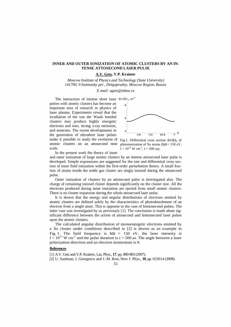
55
INNER AND OUTER IONIZATION OF ATOMIC CLUSTERS BY AN IN-TENSE ATTOSECOND LASER PULSE
A.V. Gets, V.P. Krainov
Moscow Institute of Physics and Technology (State University) 141700, 9 Institutsky per., Dolgoprudny, Moscow Region, Russia
E-mail: [email protected]
The interaction of intense short laser pulses with atomic clusters has become an important area of research in physics of laser plasma. Experiments reveal that the irradiation of the van der Waals bonded clusters may produce highly energetic electrons and ions, strong x-ray emission, and neutrons. The recent developments in the generation of ultrashort laser pulses make it possible to study the evolution of atomic clusters on an attosecond time scale.
In the present work the theory of inner and outer ionization of large atomic clusters by an intense attosecond laser pulse is developed. Simple expressions are suggested for the rate and differential cross sec-tion of inner field ionization within the first-order perturbation theory. A small frac-tion of atoms inside the noble gas cluster are singly ionized during the attosecond pulse.
Outer ionization of clusters by an attosecond pulse is investigated also. The charge of remaining ionized cluster depends significantly on the cluster size. All the electrons produced during inner ionization are ejected from small atomic clusters. There is no cluster expansion during the whole attosecond laser pulse.
It is shown that the energy and angular distributions of electrons emitted by atomic clusters are defined solely by the characteristics of photodetachment of an electron from a single atom. This is opposite to the case of femtosecond pulses. The latter case was investigated by us previously [1]. The conclusion is made about sig-nificant difference between the action of attosecond and femtosecond laser pulses upon the atomic clusters.
The calculated angular distribution of monoenergetic electrons emitted by a Xe cluster under conditions described in [2] is shown as an example in Fig. 1. The field frequency is ħω = 150 eV, the laser intensity is I = 1015 W cm-2 and the pulse duration is τ = 500 as. The angle between a laser polarization direction and an electron momentum is θ.
References
[1] A.V. Gets and V.P. Krainov, Las. Phys., 17, pp. 880-883 (2007). [2] U. Saalman, I. Georgescu and J.-M. Rost, New J. Phys., 10, pp. 025014 (2008).
pê4 pê2 3pê4 p q2
4
6
dsêdW p, 10-4
Fig.1. Differential cross section dσ/dΩp of photoionization of Xe atoms (ħω = 150 eV, I = 1015 W cm-2, τ = 500 as).
56
EFFECTS OF MAGNETIC AND NONMAGNETIC IMPURITIES ON ELECTRONIC PROPERTIES OF SEMICONDUCTOR MULTILAYERS
L. Gharaee1, A. Saffarzadeh1,2
1 Department of Physics, Payame Noor University, Nejatollahi Street, Tehran, Iran 2 Computational Physical Sciences Laboratory, Department of Nano-Science, Insti-tute for Research in Fundamental Sciences (IPM), P.O. Box 19395-5531, Tehran,
Iran
E-mail: [email protected] and [email protected]
Using the single-site coherent potential approximation (CPA) for magnetic and chemical (nonmagnetic) impurities, the electronic density of states in semiconductor multilayers is studied theoretically. The results will be presented for a multilayer which consists of five atomic layers. For this layered structure, the local density of states (LDOS) depends on the layer number and hence, the step-like features and the sharp peaks (van-Hove singularities) in the LDOS are different in various layers due to the quantum confinement of carriers along the confined direction. We find that the LDOS which depends on the impurity concentration x and the strength of disor-der varies differently in the cases of magnetic and nonmagnetic dopings.
With increasing the nonmagnetic (chemical) impurity concentration, some of the van-Hove singularities in the LDOS disappeared. In the case of donor (acceptor) impurity, by increasing x the electronic spectra are shifted to the lower (higher)-energy side and the van-Hove singularities gradually disappeared. Moreover, in the presence of magnetic impurity, the bands are broadened due to the impurity spin fluctuation, and the van-Hove singularities can completely disappear and the curves become smooth. This band broadening depends on the strength of magnetic disorder and is much larger when the interaction is stronger. The results may be useful in electronic and optoelectronic nanodevices.
References
[1] A. Gonis, Green functions for ordered and disordered systems. (North-Holland, Amsterdam) Vol. 4, (2007). [2] A. Saffarzadeh, Chemical and magnetic impurity effects on electronic properties of semiconductor quantum wirese. Phys. Rev. B 76, 214201 (2007). [3] A. Saffarzadeh and L. Gharaee, Optical absorption in disordered semiconductor multilayers. cond-mat/1001-2000.
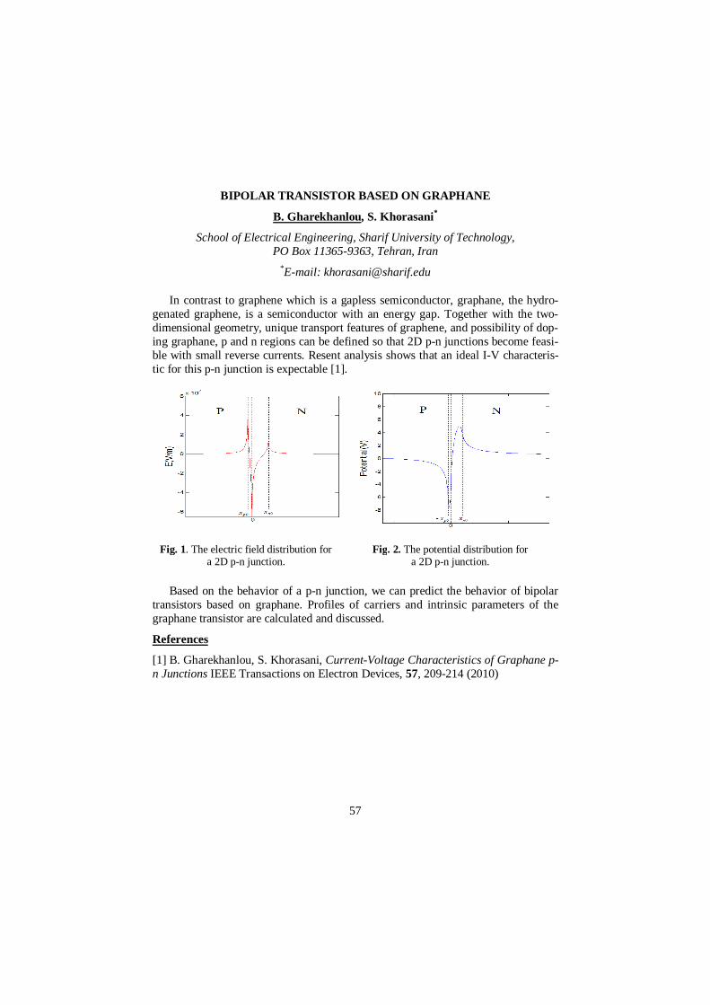
57
BIPOLAR TRANSISTOR BASED ON GRAPHANE
B. Gharekhanlou, S. Khorasani*
School of Electrical Engineering, Sharif University of Technology, PO Box 11365-9363, Tehran, Iran
*E-mail: [email protected]
In contrast to graphene which is a gapless semiconductor, graphane, the hydro-genated graphene, is a semiconductor with an energy gap. Together with the two-dimensional geometry, unique transport features of graphene, and possibility of dop-ing graphane, p and n regions can be defined so that 2D p-n junctions become feasi-ble with small reverse currents. Resent analysis shows that an ideal I-V characteris-tic for this p-n junction is expectable [1].
Based on the behavior of a p-n junction, we can predict the behavior of bipolar transistors based on graphane. Profiles of carriers and intrinsic parameters of the graphane transistor are calculated and discussed.
References
[1] B. Gharekhanlou, S. Khorasani, Current-Voltage Characteristics of Graphane p-n Junctions IEEE Transactions on Electron Devices, 57, 209-214 (2010)
Fig. 1. The electric field distribution for a 2D p-n junction.
Fig. 2. The potential distribution for a 2D p-n junction.
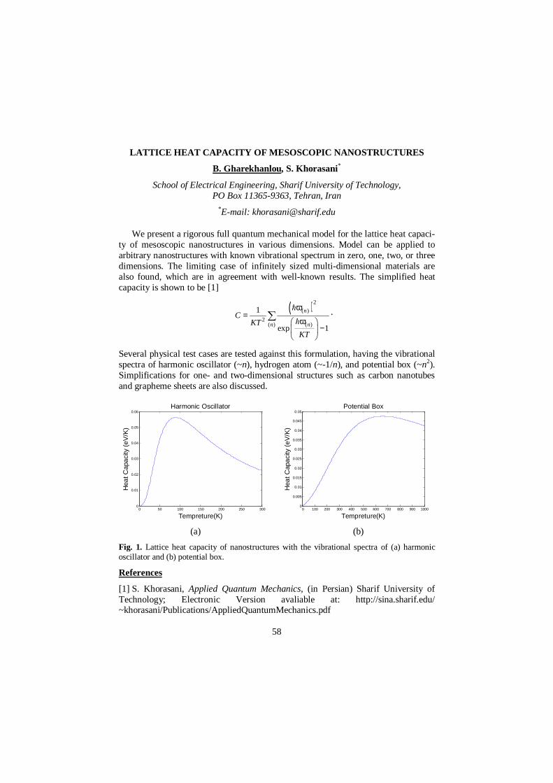
58
LATTICE HEAT CAPACITY OF MESOSCOPIC NANOSTRUCTURES
B. Gharekhanlou, S. Khorasani*
School of Electrical Engineering, Sharif University of Technology, PO Box 11365-9363, Tehran, Iran
*E-mail: [email protected]
We present a rigorous full quantum mechanical model for the lattice heat capaci-ty of mesoscopic nanostructures in various dimensions. Model can be applied to arbitrary nanostructures with known vibrational spectrum in zero, one, two, or three dimensions. The limiting case of infinitely sized multi-dimensional materials are also found, which are in agreement with well-known results. The simplified heat capacity is shown to be [1]
( )2
( )
2( )( )
1
exp 1
n
nn
CKT
KT
ω=
ω −
∑
.
Several physical test cases are tested against this formulation, having the vibrational spectra of harmonic oscillator (~n), hydrogen atom (~-1/n), and potential box (~n2). Simplifications for one- and two-dimensional structures such as carbon nanotubes and grapheme sheets are also discussed.
0 50 100 150 200 250 3000
0.01
0.02
0.03
0.04
0.05
0.06Harmonic Oscillator
Tempreture(K)
Hea
t Cap
acity
(eV
/K)
(a)
0 100 200 300 400 500 600 700 800 900 10000
0.005
0.01
0.015
0.02
0.025
0.03
0.035
0.04
0.045
0.05Potential Box
Tempreture(K)
Hea
t Cap
acity
(eV
/K)
(b)
Fig. 1. Lattice heat capacity of nanostructures with the vibrational spectra of (a) harmonic oscillator and (b) potential box.
References
[1] S. Khorasani, Applied Quantum Mechanics, (in Persian) Sharif University of Technology; Electronic Version avaliable at: http://sina.sharif.edu/ ~khorasani/Publications/AppliedQuantumMechanics.pdf
59
BROWNIAN MOTION WITH ADHESION
Moshe Gitterman
Department of Physics, Bar-Ilan University Ramat-Gan. 52900 Israel
In addition to the cases usually considered of a harmonic oscillator subject to a random force (Brownian motion) or having random frequency or random damping, we consider a random mass which corresponds to an oscillator for which some particles of the surrounding medium, adher to an oscillator for some (random) time after the collision, thereby changing the oscillator mass. This model, which describes the Brownian motion with adhesion, can be useful for the analysis of chemical and biological solutions as well as nano-technological devices. Considering dichotomous multiplicative noise and its limiting value, white noise, we have found the exact expression for the first two moments for a harmonic oscillator with a non-correlated fluctuating mass and an external noise. For the case of dichotomous fluctuations, this is equivalent to the simultaneous fluctuations of the frequency and the damping coefficient. The statistical analysis of Lyapunov exponents for fast oscillations and white noise shows that the instability occurs for large enough strength of noise. Results are compared with those obtained previously for the random frequency and random damping coefficient
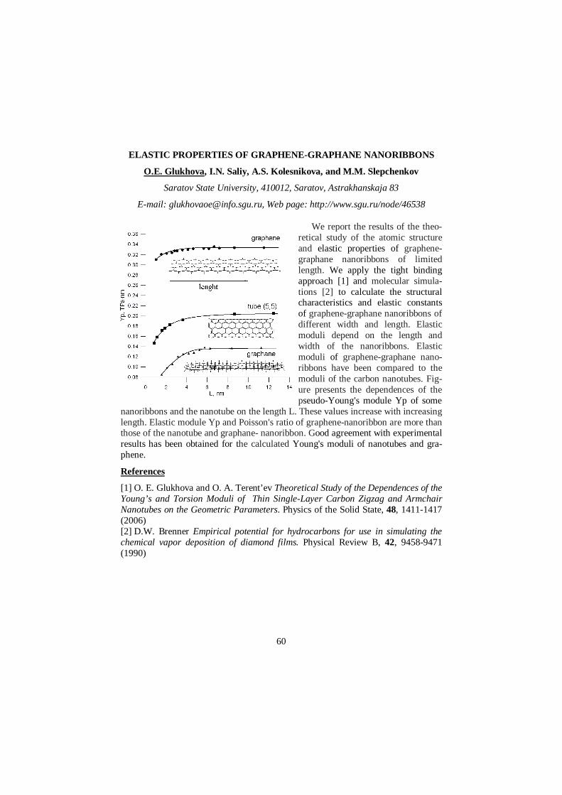
60
ELASTIC PROPERTIES OF GRAPHENE-GRAPHANE NANORIBBONS
O.E. Glukhova, I.N. Saliy, A.S. Kolesnikova, and M.M. Slepchenkov
Saratov State University, 410012, Saratov, Astrakhanskaja 83
E-mail: [email protected], Web page: http://www.sgu.ru/node/46538
We report the results of the theo-retical study of the atomic structure and elastic properties of graphene-graphane nanoribbons of limited length. We apply the tight binding approach [1] and molecular simula-tions [2] to calculate the structural characteristics and elastic constants of graphene-graphane nanoribbons of different width and length. Elastic moduli depend on the length and width of the nanoribbons. Elastic moduli of graphene-graphane nano-ribbons have been compared to the moduli of the carbon nanotubes. Fig-ure presents the dependences of the pseudo-Young's module Yp of some
nanoribbons and the nanotube on the length L. These values increase with increasing length. Elastic module Yp and Poisson's ratio of graphene-nanoribbon are more than those of the nanotube and graphane- nanoribbon. Good agreement with experimental results has been obtained for the calculated Young's moduli of nanotubes and gra-phene.
References
[1] O. E. Glukhova and O. A. Terent’ev Theoretical Study of the Dependences of the Young’s and Torsion Moduli of Thin Single-Layer Carbon Zigzag and Armchair Nanotubes on the Geometric Parameters. Physics of the Solid State, 48, 1411-1417 (2006) [2] D.W. Brenner Empirical potential for hydrocarbons for use in simulating the chemical vapor deposition of diamond films. Physical Review B, 42, 9458-9471 (1990)
61
SUPERCURRENT INTERFERENCE PATTERNS IN MULTIFACET SIFS 0- JOSEPHSON JUNCTIONS
E. Goldobin1, S. Scharinger1, C. Gürlich1, R.G. Mints2, M. Weides3, H. Kohlstedt4, D. Koelle1, and R. Kleiner1,
Physikalisches Institut -- Experimentalphysik II and Center for Collective Quantum Phenomena, Universitдt Tьbingen, Auf der Morgenstelle 14, D-72076,
Tьbingen, Germany The Raymond and Beverly Sackler School of Physics and Astronomy, Tel Aviv
University, Tel Aviv 69978, Israel Department of Physics, University of California, Santa Barbara,CA 93106, USA Nanoelektronik, Technische Fakultдt, Christian-Albrechts-Universitдt zu Kiel,
D-24143 Kiel, Germany
E-mail: [email protected]
We study the critical current dependence on applied magnetic field for Superconductor-Insulator-Ferromagnet-Superconductor Josephson junctions [1] consisting of interchanging 0 and π segments of equal lengths. The common theoretical approach [2], which assumes the uniform flux density B, predicts that: (a) Ic(H) has main maxima when the flux per segment is equal to half a flux quantum; (b) the other maxima of Ic(H) are much lower and almost symmetric relative to the main one; (c) the height of the main peaks is 0.63Ic0, where Ic0 = jcwL is the intrinsic critical current, w and L are the junction's width and length. In experiment, however, the secondary maxima between the two main maxima almost vanish and the main maxima of Ic are lower than expected. We demonstrate that these features of are caused by a non-uniform flux density B resulting from screening currents in the electrodes in the presence of a (parasitic) off-plane field component. The results reported here also may explain inconsistent experimental data obtained earlier on NCCO-NB ramp zigzag 0-π junctions [3].
References
[1] M. Weides, M. Kemmler, H. Kohlstedt, R. Waser, D. Koelle, R. Kleiner, E. Goldobin, 0- Josephson Tunnel Junctions with Ferromagnetic Barrier, Phys. Rev. Lett. 97, 247001 (2006). [2] H.-J. H. Smilde, Ariando, D. H. A. Blank, G. J. Gerritsma, H. Hilgenkamp and H. Rogalla, -Wave-Induced Josephson Current Counterflow in YBa2Cu3O7/Nb Zigzag Junctions, Phys. Rev. Lett. 88, 057004, (2002). [3] Ariando, D. Darminto, H. -J. H. Smilde, V. Leca, D. H. A. Blank, H. Rogalla and H. Hilgenkamp, Phase-Sensitive Order Parameter Symmetry Test Experiments Utilizing Nd2-xCexCuO4-y/Nb Zigzag Junctions, Phys. Rev. Lett. 94 167001 (2005).
62
THEORETICAL MODELS OF THE EXCITATION TRANSFER IN PH ASE SEPARATING LIQUIDS
A. Goun
Princeton University, 08540, Princeton, NJ, USA
E-mail: [email protected]
The use of the fluorescent resonant excitation transfer (FRET) to study the phase transition kinetics is demonstrated. The laser temperature jump is applied to the wa-ter/2,6-lutidine mixture and causes the demixing of the mixture components. Cou-marin 480 and hydroxypyrene laser dyes form excitation transfer pair once they are in the uniform phase of the mixture. Due to the differential solubility of these dyes in the components of the mixture, the excitation transfer ceases once the phase sepa-ration occurs. The increase of the donor fluorescence indicates the extent of the phase separation. The spatial resolution of the method is determined by the Forster distance of the excitation transfer pair, and in this case is equal to 3 nm. The dynam-ics of the excitation transfer between dye molecules is analyzed for Cahn-Hilliard and nucleation-growth models of phase separation.
63
QUANTUM FIELD MODEL OF THE FERROMAGNETISM IN GRAPHENE STRUCTURES
D.D. Grachev and L.A. Sevastianov
Peoples' Friendship University of Russia, 6, Mikluho-Maklaya str., Moskow, Russia
E-mail: [email protected], [email protected], Web page: http://ssalab.ru/
This work is devoted to the construction of the quantum field model, allowing, in particular, to describe ferromagnetic properties in graphen structures adequately to the results of physical and numerical experiments and its possible applications.
This nonlinear field model describes properties of monatomic graphen layers (forming two-dimensional surfaces), which are connected with presence of nontriv-ial function of distribution of the spin density, formed as a result of spontaneous breakout of the spin symmetry of valent electrons in atoms of carbon.
Within the limits of the offered model exact static and stationary decisions for the field function of the spin density, explaining, in particular, experimentally ob-served ferromagnetic properties of the graphen films are specified.
Quantitative estimations of a thickness of the domain wall, dividing areas with counter directed vectors of magnetization were suggested, which allows to check up offered theoretical model experimentally. Possible spintronic applications are dis-cussed.
64
THE APPLICATION OF ADIABATIC METHOD FOR DESCRIPTION OF IMPURITY STATES IN QUANTUM NANOSTRUCTURES
A.A. Gusev1, O. Chuluunbaatar1, S.I. Vinitsky1, E.M. Kazaryan2, H.A. Sarkisyan2
1Joint Institute for Nuclear Research, Dubna, Russia 2Russian-Armenian (Slavonic) University, Yerevan, Armenia
E-mail: [email protected], [email protected], [email protected]
In the frame of effective mass approximation the application of adiabatic method for description of impurity states in quantum dots, wires and wells with parabolic confinement potential as well as rectangular infinitely-high potential is presented. A rate of convergence of the method and efficiency of the proposed program complex, realized by the finite element method, is demonstrated on examples of calculation of spectral characteristics of the models and new effects of resonance transmission and total reflection for the Coulomb scattering, induced by axial homogeneous magnetic field, crystal channel or quantum wire [1-4].
References
[1] O. Chuluunbaatar, A.A. Gusev, V.L. Derbov, M.S. Kaschiev, L.G. Mardoyan, V.V. Serov, T.V. Tupikova and S.I. Vinitsky, Adiabatic representation for a hydro-gen atom photoionization in an uniform magnetic field, Phys. At. Nucl. 71, 844-852 (2008). [2] E.M. Kazaryan, A.A. Kostanyan, H.A. Sarkisyan Impurity optical absorption in parabolic quantum well. Physica E 28, 423-430 (2005). [3] A.A. Gusev, O. Chuluunbaatar, S.I. Vinitsky, V.L.Derbov, E. M. Kazaryan, A. A. Kostanyan, and H. A. Sarkisyan Adiabatic Approach to the Problem of a Quan-tum Well with a Hydrogen-Like Impurity. Phys. At. Nucl. 73, 331-338 (2010). [4] O. Chuluunbaatar, A.A Gusev, V.L. Derbov, P.M. Krassovitskiy and S.I. Vinit-sky, Channeling problem for charged particles produced by confining environment, Phys. At. Nucl. 72, 768-778 (2009).
65
STUDY OF CHARGE-PHASE AND CHARGE-CHARGE DIAGRAMS OF INTRINSIC JOSEPHSON JUNCTIONS
M. Hamdipour 1,2 and Yu.M. Shukrinov1
BLTP, JINR, Dubna, Moscow Region, 141980, Russia Department of physics,Institute for Advanced Studies in Basic Sciences, P.O.Box
45195-1159, Zanjan, Iran
E-mail: [email protected]
Dynamics of stacked intrinsic Josephson junctions (IJJ) in the high-Tc superconductors is theoretically investigated. The current-voltage characteristics of IJJ are numerically calculated in the framework of capacitively coupled Josephson junctions model (CCJJ model) [2,3] and capacitively coupled Josephson junctions model with diffusion current (CCJJ + DC) [1]. The breakpoint region [4] on the outermost branch of the CVC of the stacks with different number of intrinsic Josephson junctions is studied in detail. We suggest a method for investigation of the thin structure in CVC of IJJ based on the recording the diagrams "charge-phase" for given superconducting layer and "charge-charge" for different superconducting layers. It is demonstrated that this method reflects the main features in the different parts of the breakpoint region. We compare our results with the previous investigation [5,6,7] of the charge creation in superconducting layers, nucleation of the longitudinal plasma wave in the stack of IJJ and fine structure in the breakpoint region.
This research was supported by the Russian Foundation for Basic Research, grant 08-02-00520-a. References [1] T. Koyama and M. Tachiki, Phys. Rev. B 54, 16183 (1996). [2] M. Machida, T. Koyama, A. Tanaka and M. Tachiki, Physica C330, 85 (2000) [3] Yu. M. Shukrinov, F. Mahfouzi, P. Seidel. Physica C449, 62 (2006). [4] Yu. M. Shukrinov, F. Mahfouzi, Phys.Rev.Lett. 98, 157001 (2007). [5] Yu. M. Shukrinov, M. Hamdipour, M. Kolahchi, Phys.Rev.B, 80, 014512 (2008). [6] Yu. M. Shukrinov, F. Mahfouzi, M. Suzuki, Phys.Rev.B, 78, 134521 (2008) [7] Yu. M. Shukrinov, M. Hamdipour, Cond-mat. arXiv:0912.1449.
66
SUPERCONDUCTING PROXIMITY EFFECT IN GRAPHENE NANOSTRUCTURES
M. Hayashi1, H. Yoshioka2 and A. Kanda3
1Faculty of Education and Human Studies, Akita University, Akita 010-8502, Japan and JST-CREST, Kawaguchi, Saitama 332-0012, Japan
2Department of Physics, Nara Women's University, Nara 630-8506, Japan 3Institute of Physics, University of Tsukuba, Tsukuba 305-8571, Japan
E-mail:[email protected], Web page: http://www.ipc.akita-u.ac.jp/~hayashim
Supercurrent through graphene has been studied theoretically by several authors with a focus on low temperature behaviors where the band structure of graphene significantly affects the quantum transport of Cooper pairs, such as Andreev reflec-tion [1]. In this work, we study the superconducting proximity effect in nanostruc-tures including monolayer and bilayer graphene. Especially paying attention to the effects of the band structure of graphene, we study the supercurrent through the nanostructure. The supercurrent is injected and withdrawn from two attached super-conducting leads. The free energy of the superconductor-nanostructure-superconductor junction is calculated based on the tunnel Hamiltonian, and the criti-cal current through the junction and the pair amplitude in graphene are obtained. We numerically estimate the critical current for several forms of junctions and discuss the correspondence with experimental observations. The behavior of the proximity effect in monolayer system is rather close to that in normal metal, which shows monotonic dependence on temperature and junction separation. However, remarka-bly, the bilayer system shows a novel oscillating behavior as a function of tempera-ture and junction separation [2,3]. We discuss the origin of these behaviors by study-ing the pair amplitude in graphene.
References
[1] C. W. J. Beenakker, Colloquium: Andreev reflection and Klein tunneling in graphene, Rev. Mod. Phys. 80 (2008) 1337 and references therein. [2] M. Hayashi, H. Yoshioka and A. Kanda, Theoretical Study of Superconducting Proximity Eect in Single and Multi-layered Graphene, Physica C (to be published) [3] Masahiko Hayashi, Hideo Yoshioka and Akinobu Kanda, Superconducting prox-imity effect through graphene and graphite films, Journal of Physics: Conference Series 109 (2008) 012014
67
INTERMEDIATE VORTEX STATE IN NANO-SCALE ANTI-DOTS A ND MESOSCOPIC SUPERCONDUCTORS
K. Hirata, A. Thakur, and S. Ooi
National Institute for Materials Science, Superconducting Materials Center, 1-2-1 Sengen, Tsukuba, 305-0047, Japan
We have fabricated anti-dots array in Nb and NbN, and high-Tc superconductor Bi-2212 with the diameter of r and the spacing of a, and have measured the flow-resistance of vortices perpendicular to the array and magnetic field. Depending also to the ratio of r/a, we can produce a variety of vortex-matching effect; the usual and the fractional matching. In low-Tc superconductors, the usual matching effect shows "dips" in the flow resistance at the matching field. However, it shows "humps" at higher magnetic fields, which may be related to the formation of giant vortices and interstitial vortices, depending on the ratio r/a. The matching phenomena seem to occur just like the Bloch electrons in two-dimensional electron system with crystal-line lattice under magnetic field. The anti-dot array acts as a crystalline lattice to the vortices. In this case, vortex flow-resistance corresponds to Tc in the linearlized GL equation. Generation and annihilation of the fractional matching effect might be well reproduced. In high-Tc superconductor, the matching effect is closely related to the first order vortex lattice melting of the pristine samples in the presence of the anti-dot arrays and with changing the potential energy of the vortex pinning.
We also measured the vortex state in mesoscopic type I superconductors of In and Pb. This includes the observation of topological hysteresis with a signature of occurrence in different critical fields during flux entry and exit. We will show the existence of a plethora of metastable configuration and recipes to access them, and demonstrate the manifestation of superheating and supercooling of superconducting and normal states, respectively, across the superconducting transition.
68
DETECTION OF THz RADIATION FROM INTRINSIC JOSEPHSON JUNCTIONS
A. Irie, Y. Saito, M. Sakashita, K. Yamada, and G. Oya
Department of Electrical and Electronic Engineering, Utsunomiya University, Japan
We have studied terahertz emission from current-biased intrinsic Josephson junc-tions (IJJs). Large IJJ stacks, which include 100-200 junctions, with dimensions of 290×90 µm2 were formed on Bi2Sr2CaCu2Oy single crystals by standard photolithog-raphy and Ar ion milling. In order to detect terahertz radiation from these stacks, we also fabricated a small IJJ mesa with dimensions of 5×5 µm2 on a different crystal and used as detector because IJJs can also response the terahertz wave. At 4.2 K, the voltage at a constant bias current for the detector mesa were measured while scan-ning the bias voltage of the oscillator mesa. The voltage of the detector mesa showed the peaks when the voltage of the oscillator mesa was 0.12 and 0.22 V. This indicates that the oscillator mesa emits a strong radiation at these voltages. From the Josephson voltage-frequency relation, it is found that these voltages correspond 0.57 and 0.97 THz. These frequencies are not inconsistent with the cavity resonance fre-quencies.
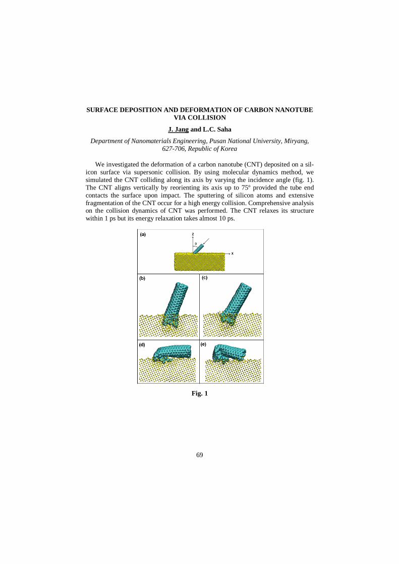
69
SURFACE DEPOSITION AND DEFORMATION OF CARBON NANOTU BE VIA COLLISION
J. Jang and L.C. Saha
Department of Nanomaterials Engineering, Pusan National University, Miryang, 627-706, Republic of Korea
We investigated the deformation of a carbon nanotube (CNT) deposited on a sil-icon surface via supersonic collision. By using molecular dynamics method, we simulated the CNT colliding along its axis by varying the incidence angle (fig. 1). The CNT aligns vertically by reorienting its axis up to 75º provided the tube end contacts the surface upon impact. The sputtering of silicon atoms and extensive fragmentation of the CNT occur for a high energy collision. Comprehensive analysis on the collision dynamics of CNT was performed. The CNT relaxes its structure within 1 ps but its energy relaxation takes almost 10 ps.
Fig. 1
70
THEORY OF ELECTRON-HOLE EXCHANGE IN SEMICONDUCTOR QUANTUM DOTS
E. S. Kadantsev1, M. Zielinski2, M. Korkusinski 1, and P. Hawrylak1
Quantum Theory Group, Institute for Microstructural Sciences, National Research Council, 1200 Montreal Rd., Ottawa, Canada K1A 0R6
Instytut Fizyki UMK, Grudziadzka 5, 87-100 Torun, Poland
E-mail: [email protected]
Efficient generation of entangled photon pairs (EPPs) ``on demand" is required for applications in quantum information processing. The major barrier to generation of EPPs is the so-called ``bright exciton splitting" originating from the long-range electron-hole exchange interaction. A k·p effective mass theory of electron-hole exchange in semiconductor quantum dots will be presented [1]. The matrix element responsible for the ``bright" exciton splitting in the effective exciton Hamiltonian is identified and analyzed. An excitonic fine structure for a model quantum dot with quasi-two-dimensional anisotropic harmonic oscillator (2DLAHO) confining potential is considered as a function of the shape anisotropy, size, and external fields. Assumptions and limitations surrounding the application of the effective approach to the calculation of excitonic fine structure will be discussed and elucidated with atomistic empirical-tight binding calculations using QNANO computational platform [2].
References
[1] E. Kadantsev and P. Hawrylak, Theory of exciton fine structure in semiconductor quantum dots: Quantum dot anisotropy and lateral electric field. Phys. Rev. B 81, 045311 (2010). [2] M. Korkusinski, M. Zielinski, and P. Hawrylak, Multiexciton complexes in InAs self-assembled quantum dots. J. Appl. Phys. 105, 122406 (2009).
71
CROSSED ANDREEV REFLECTION IN MULTITERMINAL SUPERCONDUCTING HYBRID STRUCTURES
Mikhail S. Kalenkov1, Dmitri S. Golubev2, and Andrei D. Zaikin2,1
I.E. Tamm Department of Theoretical Physics, P.N. Lebedev Physical Institute, 119991 Moscow, Russia
Forschungszentrum Karlsruhe, Institut fьr Nanotechnologie, 76021, Karlsruhe, Germany
E-mail: [email protected]
We develop a quantitative theory of electron transport in three terminal normal-superconducting-normal (NSN) structures. Subgap electrons entering S-electrode from one N-metal may form Cooper pairs with their counterparts penetrating from another N-metal. This phenomenon of crossed Andreev reflection (CAR) and normal scattering at SN interfaces are two mechanisms of the charge transfer in considered structure.
In diffusive limit local and non-local conductances were evaluated non-perturbatively at arbitrary interface transmissions. At low temperature non-local resistance becomes universal and doesn't depend on barriers resistances and parameters of the normal terminals. For instance, in quasi one-dimensional geometry nonlocal resistance takes the following form
ξ−ξ= /12 2
der
R ,
where ξ is zero temperature superconducting coherence length, d is the distance between NS contacts, and rξ is Drude (normal state) resistance of the segment of S-metal with lengths ξ. It is well known that interplay of the Andreev reflection and disorder induced scattering leads to zero bias anomaly in conductance of NS junctions. We show that similar anomaly appears in non-local conductance.
Local and nonlocal transport in hybrid superconducting structures is very sensitive to the presence of ferromagnetism in the normal terminals. In particular, in ferromagnet-superconductor-ferromagnet structure nonlocal resistance is no longer universal and depends on mutual polarization of the ferromagnets and zero bias anomaly is strongly suppressed by exchange field both in local and nonlocal conductances.
Our predictions are in a good agreement with recent experimental observations.
References
[1] D.S. Golubev, M.S. Kalenkov, A.D. Zaikin, Phys. Rev. Lett. 103, 067006 (2009).
72
GEOMETRIC SHAPE EFFECTS ON FIELD EMISSION FOR AXISYMMETRIC AND WALL-LIKE EMITTERS
V.L. Katkov and V.A. Osipov
Bogoliubov Laboratory of Theoretical Physics, Joint Institute for Nuclear Research, 141980 Dubna, Moscow region, Russia
E-mail: [email protected]
The Fowler-Nordheim (FN) theory is extended to include a potential distribu-tion outside an axisymmetric ellipsoid and a wall with a semi-elliptical shape. The tips of nanometric radii, are considered. The variation in emission over the surface is taken into account by effective emission area. The FN slopes are found to be mark-edly larger in comparison with those predicted by the standard FN theory. Analysis of experimental observed slope can provides information about geometrical charac-teristic of emitters. It is shown that for wall-like emitters the geometrical effects are less pronounced in comparison with the axisymmetric emitters.
73
VORTEX DYNAMICS IN FINITE SUPRECONDUCTING NETWORKS AND COMPOSITE STRUCTURES OF D- AND S-WAVE SUPERCONDUC-
TORS (D-DOT)
M. Kato1,6, O. Sato2, T. Koyama3,6, M. Machida4,6, and T. Ishida5,6
1Department of Mathematical Sciences, Osaka Prefecture University, 1-1, Gakuen-cho, Nakaku, Sakai, Osaka 599-8531, Japan
2 Department of Liberal Arts, Osaka Prefectural College of Technology, 26-12 Sai-wai-cho, Neyagawa, Osaka 572-8572, Japan
3IMR, Tohoku University, 2-1-1 Katahira Aoba-ku, Sendai 980-8577, Japan 4 CCSE, JAEA, 6-9-3 Higashi-Ueno Taito-ku, Tokyo 110-0015, Japan
5 Department of Physics and Electronics, Osaka Prefecture University, 1-1, Gakuencho, Nakaku, Sakai, Osaka 599-8531, Japan
6 CREST, JST, 5, Sanbancho, Chiyoda-ku, Tokyo 102-0075, Japan
E-mail: [email protected], Web page http://www.ms.osakafu-u.ac.jp/~kato/index.html
We investigated the vortex dynamics in several nano-sized superconductors. In finite superconducting networks, we found peculiar vortices, such as giant
vortex and anti vortex [1,2]. And, we investigated the dynamics of vortices in the asymmetric finite networks under the external AC current using the time-dependent Ginzburg-Landau (GL) equation. And found the rectified motion of vortices, which depends on the external magnetic field, temperature and the amplitude of the AC current [3].
In a composite structure of d- and s-wave superconductors (d-dot), we showed the appearance of the spontaneous half-quantum magnetic flux, using the two-components GL equation. We proposed a cellar automata-like logic gate using these half-quantum vortices, and simulated the operation of this gate [4].
References
[1] O. Sato and M. Kato, Inhomogeneous Superconducting State of Superconducting Networks in a Magnetic Field, Phys. Rev. B, 68, 094509 (2003) . [2] M. Kato Y. Iwamoto, O. Sato, Vortex structures in disordered finite superconducting square networks under external magnetic field, Phys. Rev. B 80, 024510 (2009) [3] M. Kato, O. Sato, M. Hayashi, H. Ebisawa, T. Koyama, M. Machida, T. Ishida , Vortex dynamics in asymmetric superconducting networks, Physica C 468, 1249 (2008) [4] S. Nakajima, M. Kato, T. Koyama, M. Machida, T. Ishida, F. Nori, Simulation of logic gate using d-dot's", Physica C, 468, 769 (2008)
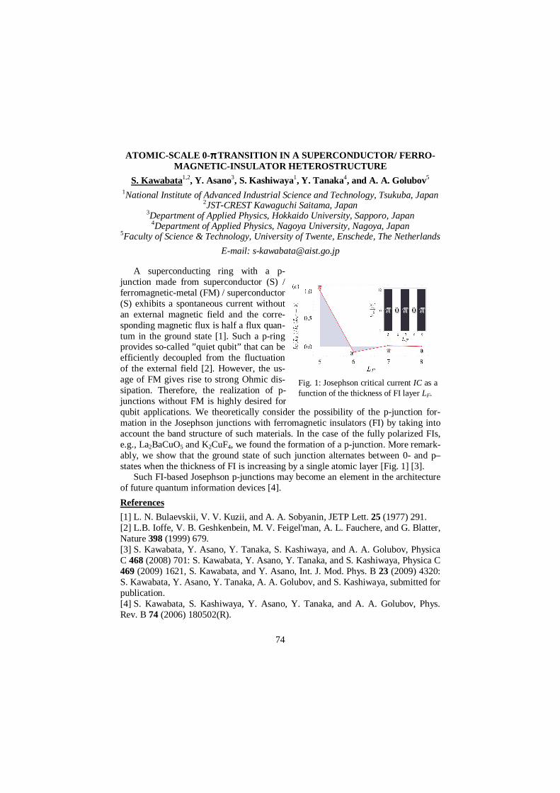
74
ATOMIC-SCALE 0- ππππ TRANSITION IN A SUPERCONDUCTOR/ FERRO-MAGNETIC-INSULATOR HETEROSTRUCTURE
S. Kawabata1,2, Y. Asano3, S. Kashiwaya1, Y. Tanaka4, and A. A. Golubov5
1National Institute of Advanced Industrial Science and Technology, Tsukuba, Japan 2JST-CREST Kawaguchi Saitama, Japan
3Department of Applied Physics, Hokkaido University, Sapporo, Japan 4Department of Applied Physics, Nagoya University, Nagoya, Japan
5Faculty of Science & Technology, University of Twente, Enschede, The Netherlands
E-mail: [email protected]
A superconducting ring with a p-junction made from superconductor (S) / ferromagnetic-metal (FM) / superconductor (S) exhibits a spontaneous current without an external magnetic field and the corre-sponding magnetic flux is half a flux quan-tum in the ground state [1]. Such a p-ring provides so-called ”quiet qubit” that can be efficiently decoupled from the fluctuation of the external field [2]. However, the us-age of FM gives rise to strong Ohmic dis-sipation. Therefore, the realization of p-junctions without FM is highly desired for qubit applications. We theoretically consider the possibility of the p-junction for-mation in the Josephson junctions with ferromagnetic insulators (FI) by taking into account the band structure of such materials. In the case of the fully polarized FIs, e.g., La2BaCuO5 and K2CuF4, we found the formation of a p-junction. More remark-ably, we show that the ground state of such junction alternates between 0- and p–states when the thickness of FI is increasing by a single atomic layer [Fig. 1] [3].
Such FI-based Josephson p-junctions may become an element in the architecture of future quantum information devices [4].
References
[1] L. N. Bulaevskii, V. V. Kuzii, and A. A. Sobyanin, JETP Lett. 25 (1977) 291. [2] L.B. Ioffe, V. B. Geshkenbein, M. V. Feigel'man, A. L. Fauchere, and G. Blatter, Nature 398 (1999) 679. [3] S. Kawabata, Y. Asano, Y. Tanaka, S. Kashiwaya, and A. A. Golubov, Physica C 468 (2008) 701: S. Kawabata, Y. Asano, Y. Tanaka, and S. Kashiwaya, Physica C 469 (2009) 1621, S. Kawabata, and Y. Asano, Int. J. Mod. Phys. B 23 (2009) 4320: S. Kawabata, Y. Asano, Y. Tanaka, A. A. Golubov, and S. Kashiwaya, submitted for publication. [4] S. Kawabata, S. Kashiwaya, Y. Asano, Y. Tanaka, and A. A. Golubov, Phys. Rev. B 74 (2006) 180502(R).
Fig. 1: Josephson critical current IC as a function of the thickness of FI layer LF.
75
AGGLOMERATION MODEL OF CARBON NANOSTRUCTURES *)
R. Kerner
Laboratoire de Physique Théorique de la Matière Condensée, Université Pierre et Marie Curie (Paris-VI), Paris, France.
We present a model of agglomeration of carbon clusters from small molecular fragments torn out from graphite at high temperature. The bond-bending energies of such clusters, especially those containing pentagonal and hexagonal rings, are taken into account and used in the Boltzmann factors corresponding to each step of ag-glomeration. Probabilities of clusters with growing number of carbon atoms are cal-culated. The principles of self-similarity and least free energy can be then applied. The self-similarity requirement means that the growing clusters tend to conserve their local curvature; the least free energy means minimizing the bond-bending con-tributions.
These two hypotheses provide a good insight into the statistics of various types of clusters depending also on the temperature. The relative yield of various fuller-enes and graphene fragments can be then estimated.
*) This work develops the ideas exposed in my recent book R.Kerner, “Models of Agglomeration and Glass Transition”, Imperial College Press 2007
76
NANOPARTICLE SIZING AND LATE STAGE FUSION DURING MA TRIX DIFFUSION: A MATHEMATICAL MODELING STUDY
R.A. Khan1* and V. Rai2
1Department of Chemistry 2Department of Mathematics, Manav Rachna International University (MRIU), Sec-
tor-43, Aravali Hills, Faridabad, HR, India
Keywords: Nanoparticle, Kinetics, Viscosity, Sizing, Fusion, Differential Equation, Numerical Simulation
The nascent nanoparticle formation in the colloidal vesicle and its differentiation into respective uniform-sized nanoparticles is a fundamental question in the for-mation of the nanomaterials involving the particulate matter. Diffusion alone does not play the role in its distribution over the matrix which seemingly to us is a frac-tionated and initially as well as penultimately is a well-ordered structure for major time-fraction of the synthesis. The size distribution is governed by a threshold limit decided by viscosity of the matrices and density of the formed nanoparticles in the reaction decided by the prevalent kinetics of the reactants and product. Moreover, further size distribution from initial sizing to later stage sizes is dominated by the disturbance in the distribution pattern owing to space limitation in the changing den-sity of the inherent medium which follows a random pattern. The pattern keeps changing with time and particle drift decides the ultimate stage nanoparticle’s size-fusion and early agglomeration.
A mathematical model is proposed to represent nanoparticle sizing and late stage fusion. The systems of differential equations are studied using numerical simulation which uses Runge-Kutta 4.
77
SHEET CURRENT MODEL FOR INDUCTANCES EXTRACTION AND JOSEPHSON JUNCTIONS DEVICES SIMULATION
M.M. Khapaev1 and M.Yu. Kupriyanov 2
1 Dep. of Numerical Methods, VMK, Moscow State University, Vorob'evy Gory, 119992, Moscow, Russia
2 Laboratory for Physics of Nanostructures, Institute of Nuclear Physics Moscow State University, 119992 Vorob'evy Gory, Moscow, Russia
E-mail: [email protected], http://vm.cs.msu.su/
Sheet current model for microelectronic superconductor structures, based on Maxwell and London equations, is presented. In this model, magnetic field is three-dimensional but resulting integro-differential equations for current density potential are two-dimensional. These equations are solved using finite element method and matrix of self and mutual inductances is calculated as well as current distribution in superconductors. Then, current distribution can be used for calculation of boundary conditions for Josephson junctions equations. In particular we apply this approach for calculations of bias and control line currents for flux flow oscillator simulation problem. The program and results of calculations are presented.
References
[1] M. M. Khapaev, IEEE Trans. Microwave Theory and Techn., 2001 49, pp. 217-220. [2] M. M. Khapaev, M. Yu. Kupriyanov, E. Goldobin, M. Siegel, Supercond. Sci. Technol. – 2003. - 16. - P. 24-27. [3] V. P. Koshelets, J. Mygind Flux flow oscillators for super-conducting integrated submm wave receivers. Studies of High Temperature Superconductors, 39, P. 213–244, March 2001. ed. A.V. Narlikar, NOVA Science Publishers, New York. [4] M. M. Khapaev, M. Yu. Kupriyanov New ideas for long Josephson junctions realistic devices simulation J. Phys.: Conf. Ser. 2008, 129 012037 (8pp).
78
EXPERIMENTAL OBSERVATION OF THE INVERSE PROXIMITY E F-FECT IN THE SUPERCONDUCTOR/FERROMAGNET BILAYER
Yu.N. Khaydukov1, K.N. Zhernenkov1,2, Yu.V. Nikitenko1, B. Nagy3, L. Bottyan3, R. Steitz4, A. Teichert4, A. Rühm5 and V.L. Aksenov1
1Joint Institute for Nuclear Research, Dubna, Russia 2Ruhr-Universität Bochum, Bochum, Germany
3KFKI Research Institute for Particle and Nuclear Physics, Budapest, Hungary 4Helmholtz-Zentrum für Materialien und Energie, Berlin, Germany
5Max-Planck-Institut für Metallforschung, Stuttgart, Germany
Penetration of the superconducting order parameter inside ferromagnet metal in superconducting/ferromagnet (S/F) heterostructures is classically called proximity effect. Theoretically it was also predicted inverse proximity effect - the appearance of the induced magnetization in S layer near the S/F interface. This effect is dis-cussed in various theoretical works, where it is shown that the induced magnetiza-tion can have both positive and negative sign to the magnetization in the F layer [1-3].
In this work we present the first experimental observation of the inverse proximi-ty effect done by the polarized neutron reflectometry on the system Cu(32 nm)/V(40 nm)/Fe(1 nm)/MgO. Here vanadium is superconducting layer with transition tem-perature TC = 3.5K, iron is ferromagnetic layer with Curie temperature of about 400-500K. The S/F is placed between layers Cu and MgO to create waveguide enhanced regime of neutron scattering [4]. This regime allowed to increase sufficiently weak neutron scattering from magnetic potential and allowed to observe induced magneti-zation with positive sign in S layer close to the S/F interface. Possible explanation of the results based on the theory of the inverse proximity effect in ballistic limit [3] is discussed.
References
[1] V.N. Krivoruchko and E.A. Koshina, Phys. Rev. B 66, 014521 (2002) [2] F.S. Bergeret, A.F. Volkov and K.B. Efetov, Phys.Rev. B 69, 174504 (2004) [3] F.S. Bergeret, A. Levy Yeyati and A. Martin-Rodero, Phys. Rev. B 72, 064524 (2005) [4] Yu. N. Khaydukov, K.N. Zhernenkov, Yu.V. Nikitenko,, L. Bottyan, A. Rühm, and V.L. Aksenov accepted to Cryst. Rep., e-preprint: arXiv:1001.2895
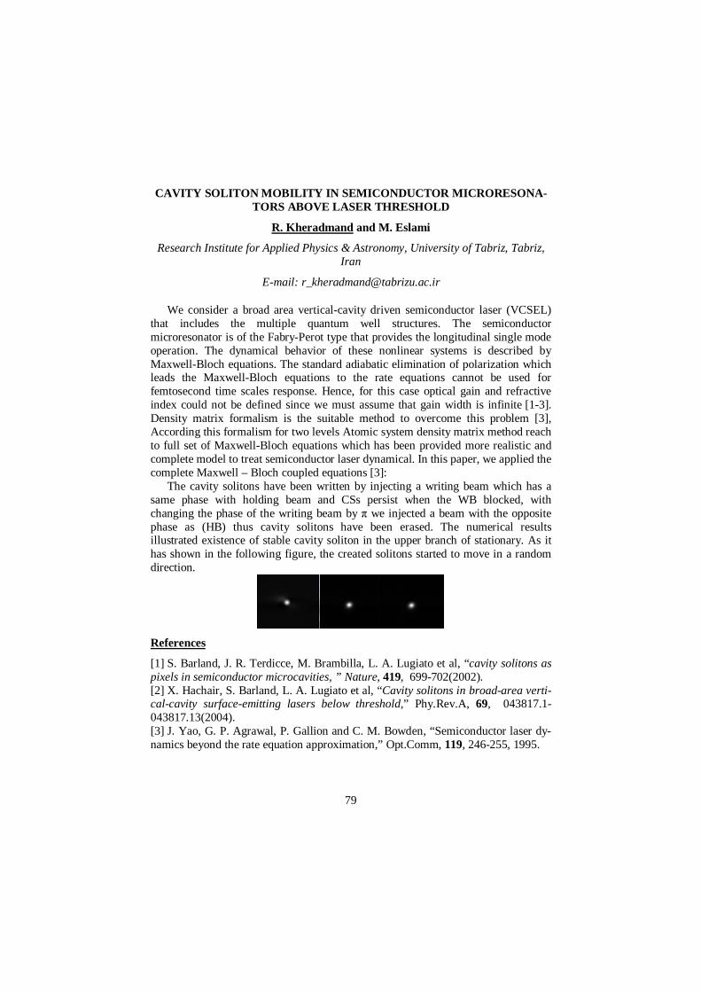
79
CAVITY SOLITON MOBILITY IN SEMICONDUCTOR MICRORESON A-TORS ABOVE LASER THRESHOLD
R. Kheradmand and M. Eslami
Research Institute for Applied Physics & Astronomy, University of Tabriz, Tabriz, Iran
E-mail: [email protected]
We consider a broad area vertical-cavity driven semiconductor laser (VCSEL) that includes the multiple quantum well structures. The semiconductor microresonator is of the Fabry-Perot type that provides the longitudinal single mode operation. The dynamical behavior of these nonlinear systems is described by Maxwell-Bloch equations. The standard adiabatic elimination of polarization which leads the Maxwell-Bloch equations to the rate equations cannot be used for femtosecond time scales response. Hence, for this case optical gain and refractive index could not be defined since we must assume that gain width is infinite [1-3]. Density matrix formalism is the suitable method to overcome this problem [3], According this formalism for two levels Atomic system density matrix method reach to full set of Maxwell-Bloch equations which has been provided more realistic and complete model to treat semiconductor laser dynamical. In this paper, we applied the complete Maxwell – Bloch coupled equations [3]:
The cavity solitons have been written by injecting a writing beam which has a same phase with holding beam and CSs persist when the WB blocked, with changing the phase of the writing beam by π we injected a beam with the opposite phase as (HB) thus cavity solitons have been erased. The numerical results illustrated existence of stable cavity soliton in the upper branch of stationary. As it has shown in the following figure, the created solitons started to move in a random direction.
References
[1] S. Barland, J. R. Terdicce, M. Brambilla, L. A. Lugiato et al, “cavity solitons as pixels in semiconductor microcavities, ” Nature, 419, 699-702(2002). [2] X. Hachair, S. Barland, L. A. Lugiato et al, “Cavity solitons in broad-area verti-cal-cavity surface-emitting lasers below threshold,” Phy.Rev.A, 69, 043817.1-043817.13(2004). [3] J. Yao, G. P. Agrawal, P. Gallion and C. M. Bowden, “Semiconductor laser dy-namics beyond the rate equation approximation,” Opt.Comm, 119, 246-255, 1995.
80
STUDY OF ALL OPTICAL SWITCHING BEHAVIOR IN SEMICONDU C-TOR MICRORESONATOR WITH NANO-ACTIVE LAYER
R. Kheradmand and H. Aryan
Research Institute for Applied Physics & Astronomy, University of Tabriz, Tabriz-Iran
E-mail: [email protected]
In this paper we study required perturbation coefficient for switching between two state in our all optical switch that is based on controlling optical patterns[1-3] in semiconductor microresonator with nano layer as an active media.
In semiconductor microresonator devices optical patterns emerge from the coupling of the nonlinear medium response, diffraction, and the feedback action of mirrors. First of all we presented results of our switching for experimental parameters according to reference [3], and after that we optimized all optical switches with study of different fundamental parameters in our system.
In this paper all optical switches that are based on control of transverse optical patterns have been investigated. A semiconductor microresonator in active configuration has been considered for patterns formation. Also to perform switching a spatial perturbation as modulated input field amplitude has been injected to the system. Behavior of carriers in spontaneous patterns formation and patterns switching has been studied. We explored performance of system in patterns formation and switching with respect to fundamental physical characteristics of system.
Results demonstrate that with increasing length of cavity the range of required input field amplitude for patterns formation increased slightly and also the minimum perturbation coefficient for switching decreased greatly. Increasing nonradiative recombination rate of carriers about ten percent appeared that required input field amplitude for patterns formation raised more than before, albeit the minimum perturbation coefficient for switching and switching and switching time dose not vary considerably.
References
[1] A.M.C. Dawes, L. Illing, S.M. Clark, D.J. Gauthier, All-Optical Switching in Rubidium Vapor, Science 308, 672 (2005). [2] Kheradmand, R., et al. All optical switching in semiconductor microresonators based on pattern selection, Eur. Phys. J. D, 47, 107-112 (2008). [3] Reza Kheradmand et al. Optical Pattern Switching in Semiconductor Microreso-nators as All-Optical Switch, ETRI Journal, 31, 5 (2009).
81
MASSIVE DIRAC FERMIONS IN GRAPHENE
D.V. Khveshchenko
Department of Physics and Astronomy, University of North Carolina, Chapel Hill, NC 27599, USA
Recent advances in microfabrication of graphene have made it possible to test the low-energy quasiparticle excitations in this system which can be described as Dirac fermions carrying an additional orbital ("valley") quantum number, besides the physical spin 1/2. In this work, we focus on the effects of strong Coulomb corre-lations and disorder, drawing some insightful parallels with the phenomena of chiral symmetry breaking and magnetic catalysis in relativistically invariant 2+1-dimensional fermion theories. We make a number of specific experimental predic-tions and compare them with the available results of tunneling, photoemission, and magnetization measurements, as well as Monte Carlo simulations.
82
LIPID NANOSTRUCTURES
M.A. Kiselev
Frank Laboratory of Neutron Physics, Joint Institute for Nuclear Research, Dubna, Russia
E-mail: [email protected]
Lipids are important component in the formulation of drug nanoparticles, drug carries, pharmaceutical and cosmetic creams. The results of structural investigation of lipid nanostructures are presented for two types of lipids: phospholipids (main component of plasma membrane) and ceramides (main component of the lipid ma-trix of stratum corneum). Experiments were carried out by neutron and X-ray scat-tering at different European neutron and synchrotron centers.
The theoretical problems are discussed related to the: • Membrane self assembly in the mixed phospholipid/ detergent systems and
stability of the mixed phospholipid/detergent vesicles in the process of drug delivery through the skin [1]
• Super-strong membrane interaction created by ceramide 6 molecules in the lipid matrix of stratum corneum (mechanical and diffusion properties of the skin) [2].
• Phase diagram of the spontaneous curvature of the phospholipid unilamel-lar vesicles [3]
References
[1] М.A. Kiselev, D. Lombardo, P. Lesieur , A.M. Kisselev, S. Borbely, T.N. Si-monova, L.I. Barsukov. Membrane Self Assembly in Mixed DMPC/NaC Systems by SANS. Chemical Physics 345 173-180 (2008) [2] M. A. Kiselev, N. Yu. Ryabova, A. M. Balagurov, S. Dante, T. Hauss, J. Zbyto-vska, S. Wartewig, R. H. H. Neubert. New insights into structure and hydration of stratum corneum lipid model membrane by neutron diffraction. European Biophys. J. 34 1030–1040 (2005) [3] М.А. Kiselev, E.V. Zemlyanaya, V.K. Aswal, R.H.H. Neubert. What can we learn about the lipid vesicle structure from the small angle neutron scattering exper-iment? European Biophys. J. 35 477-493 (2006)
83
STRUCTURE, QUANTUM EFFECTS AND MAGNETISM IN PD CON-TACTS
A.L. Klavsyuk, S.V. Kolesnikov, and A.M. Saletsky
Faculty of Physics, Moscow State University, 119991, Russian Federation
Palladium is one of the most intriguing and controversial material, which could exhibit magnetic properties in nanocontact by small variations of external parame-ters. Quantum point contacts are structures in which a neck of atoms just a few atomic diameters wide bridges two electrodes. Our approach is based on density functional theory Vienna Ab-initio Simulation Package (VASP) and Molecular-dynamics method. Atomic relaxations of nanocontacts and electrodes are calculated with ab initio based many body potentials for low-dimensional systems. We con-centrate on Pd atomic bridges. The main goal of the present study is to understand the role of linear sizes, orientation and temperature in evolution of the contact and reveal the interplay between the stability of nanocontacts, stress and electronic struc-ture. Using molecular dynamics simulations we have shown that the formation of the contact strongly sensitive to the sizes and orientation. The standing-wave pat-terns that are confined within the 1D bridges allows one to explain the changes in the electronic states of bridges. We show that the atomic bridges constructed from non-magnetic in bulk Pd can be magnetic.
84
IMAGING HOT SPOTS AND THz WAVES IN INTRINSIC JOSEPHSO N JUNCTIONS
R. Kleiner1, S. Guénon1, B. Gross1, M. Grünzweig1, D. Koelle1, H. Wang2, J. Yuan2, A. Iishi2, T. Hatano2, Z. Jiang3, Y. Zhong3, P. Wu3
1Physikalisches Institut & Center for Collective Quantum Phenomena Universität Tübingen, D-79076 Tübingen, Germany
2Nano Quantum Electronics Group, Exploratory Nanotechnology Research Labora-tory, National Institute for Materials Science, 1-2-1 Sengen, Tsukuba, Ibaraki 305-
0047 Japan 3Research Institute of Superconductor Electronics, Nanjing University, Nanjing
210093, China
Having small sized active and tunable devices operating at frequencies up to the Terahertz (THz) range is one of the goals of modern electronics. However, there is still a lack of good active or passive devices, often referred to as the "Terahertz gap". Intrinsic Josephson junctions formed by the layered crystal structure of high temper-ature superconductors such as Bi2Sr2CaCu2O8 have the potential to operate in this regime. While for a long time the research on THz generation with this type of junc-tions was carried out with perhaps only modest success, recently synchronous emis-sion, with an estimated output power in the µW range, of stacks consisting of sever-al hundred intrinsic Josephson junctions was achieved [1]. We report on the investi-gation of THz electromagnetic wave generation in intrinsic junction stacks of differ-ent geometries, using a combination of transport measurement, direct electromagnet-ic wave detection and Low Temperature Scanning Laser Microscopy [2].
References
[1] L. Ozyuzer, A. E. Koshelev, C. Kurter, N. Gopalsami, Q. Li, M. Tachiki, K. Kadowaki, T. Yamamoto, H. Minami, H. Yamaguchi, T. Tachiki, K. E. Gray, W.-K. Kwok, and U. Welp, Science 318, 1291 (2007), see also R. Kleiner, Science 318, 1254 (2007). [2] H. B. Wang, S. Guénon, J. Yuan, A. Iishi, S. Arisawa, T. Hatano, T. Yamashita, D. Koelle, and R. Kleiner, Phys. Rev. Lett. 102, 017006 (2009).
85
INSTABILITY OF THE NEMATIC LIQUID CRYSTAL FILLED WIT H SPHERE-LIKE MAGNETIC-IMPURITY PARTICLES AGAINST FOR -
MATION OF THE MODULATED STRUCTURES
A.V. Kleshchonok
Kyiv National Taras Shevchenko University, 64, Vladymirska St., 01601, Kyiv, Ukraine
E-mail: [email protected]
In the last decade, much attention has been attracted to Filled Liquid Crystals . highly disperse suspension of impurity particles in nematic liquid carrier. The tested objects are filled nematic liquid crystals.highly-disperse suspension of impurity na-noparticles within the nematic liquid carrier. The spatial distribution of rigid-sphere-like magnetic-impurity nanoparticles within the host nematic liquid crystal is stud-ied. Both the indirect effective interaction between the impurity particles by means of nematic medium and the direct magnetic interaction are considered as being re-sponsible for the formation of (modulated) superstructures. In the general case, total interaction between the impurity nanoparticles includes two contributions.Van der Waals-type direct interaction (at short distances between the particles) and magnetic one as well as indirect interactions (through both the director-field distortions and the density inhomogeneities. The last one depends on temperature, density of nemat-ic host medium and impurities. concentration. As shown, there are long-range and quasi-oscillation characters of such an interaction in its energy dependence on the distance between impurity particles. This effective interaction controls the structure formation and properties of a system. Using continuum-mechanics and statistical-thermodynamics approaches, we analyze the necessary thermodynamic conditions for formation of modulated lamellar structures. This condition allows to calculate temperature of homogeneous-distribution stability loss and to estimate period of formed structure along direction of undistorted director. Results of calculations are in a qualitative agreement with available experimental data and computer simula-tions. The offered theoretical approach can be used to forecasting other anisotropic and inhomogeneous mesomorphic systems, which can find application by develop-ment of integrated-optics facilities to govern the light-beam passing (diffraction gratings of an optical range etc.).
86
TOWARDS TERAHERTZ JOSEPHSON RADIATION SOURCES: RECENT RESULTS
A.M. Klushin 1, F. Song1,2, A.D. Semenov3 and V.V. Kurin 4
1Institute for Bio- and Nanosystems and JARA - Fundamentals of Future Infor-mation Technologies, Forschungszentrum Juelich GmbH, Juelich, Germany
2Department of Electronics, Nankai University, Tianjin, P. R. China 3Institute of Planetary Research, German Aerospace Center, 12489 Berlin, Germany
4Institute for Physics of Microstructures RAS, Nizhniy Novgorod 603950, Russia
E-mail: [email protected]
In the talk recent results of our work towards continues wave teraherz radiation sources based on arrays of discrete Josephson junctions will be summarized. Self-radiation from arrays of low-temperature [1] and high-temperature superconductor junctions [2], embedded in an open quasioptical resonator will be discussed. We have explored the millimeter wave radiation from our Josephson junction arrays embedded in a quasioptical resonator. Radiation from arrays was detected by a low noise superheterodyne receiver at frequency about 80 GHz and liquid nitrogen and helium temperatures. Also the new results of the measurements with broadband de-tectors [3] will be presented. To explain the coherent behavior of the array of Jo-sephson junctions electromagnetic field simulations were performed. Considering the substrate as a dielectric resonator antenna, the coherent emission was excited if the location of each subarray coincided with the positions of the maximum electric field intensity in the substrate resonance mode. The linewidth of the self-radiation, microwave coupling and impedance matching with a quasioptical resonator will be discussed at the Conference.
References
[1] F. Song, F. Müller, R. Behr, A.M. Klushin, Coherent emission from large arrays of discrete Josephson junctions, Appl. Phys. Lett., 95, 172501 (2009). [2] F. Song, M. Levitchev, V. Markelov, V.V. Kurin, L. Fang, A.M. Klushin, Millimeter wavelength radiation from arrays of discrete high-temperature superconductor Josephson junctions, Superc. Scienc. Technolog, accepted for publication (2010). [3] A. Semenov, O. Cojocari, H.-W. Hübers, F. Song, A. Klushin, A.-S. Müller, Applications of Zero-Bias Quasioptical Schottky-Diode Detectors for Monitoring Short-Pulse & weak THz radiation, IEEE Electr. Dev. Lett., submitted for publication (2010).
87
PHOTONIC BAND STRUCTURE CALCULATION AND OPTICAL ABSORPTION MODELING OF THE COPPER CARBON COMPOSITE NANOLAYER BASED ON THE 3D LATTICE OF COUPLED DIPOLES
A. Kokabi1, M. Hoseini2, A. Moftakharzadeh1, M. A. Vesaghi2, M. Fardmanesh1 1Department of Electrical Engineering, Sharif University of Technology, Tehran,
Iran 2Physics Department, Sharif University of Technology, Tehran, Iran
Email: [email protected]
Absorption coefficient and photonic band structure for a cubic lattice of metallic nanoparticles have been calculated. The applied method for this calculation is based on three-dimensional extension of the one-dimensional model for the chain of Hertzian nanoparticle dipoles. In this approach, metallic nanoparticles are treated as coupled electric dipoles. Three dimensional particular equation of motion is obtained in the presence of the propagating electromagnetic wave by the approximation of the nearest neighbor interaction of dipoles. The propagating wave solution of this equation led to coupled equations for absorption coefficient and photonic band structure of the metallic nanoparticle lattice. These coupled equations are solved numerically and absorption coefficient is obtained versus wavelength for different nanoparticle sizes and lattice constants. The absorption spectrum of a copper-carbon nanocomposite that is a lattice of copper nanoparticles in the bulk diamond-like carbon is also measured. The analytical results for absorption spectrum are compared with experimental data and result of the previously published one-dimensional model.
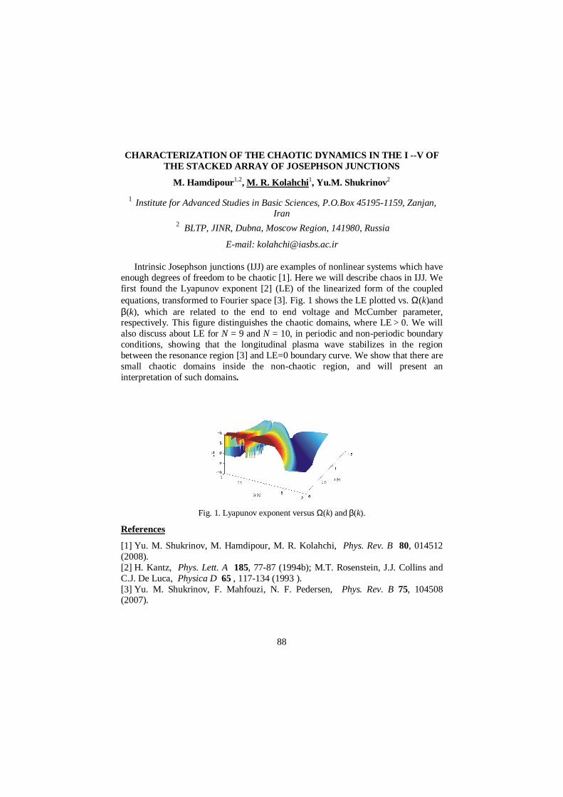
88
CHARACTERIZATION OF THE CHAOTIC DYNAMICS IN THE I - -V OF THE STACKED ARRAY OF JOSEPHSON JUNCTIONS
M. Hamdipour 1,2, M. R. Kolahchi1, Yu.M. Shukrinov2
1 Institute for Advanced Studies in Basic Sciences, P.O.Box 45195-1159, Zanjan, Iran
2 BLTP, JINR, Dubna, Moscow Region, 141980, Russia
E-mail: [email protected]
Intrinsic Josephson junctions (IJJ) are examples of nonlinear systems which have enough degrees of freedom to be chaotic [1]. Here we will describe chaos in IJJ. We first found the Lyapunov exponent [2] (LE) of the linearized form of the coupled equations, transformed to Fourier space [3]. Fig. 1 shows the LE plotted vs. Ω(k)and β(k), which are related to the end to end voltage and McCumber parameter, respectively. This figure distinguishes the chaotic domains, where LE> 0. We will also discuss about LE for N = 9 and N = 10, in periodic and non-periodic boundary conditions, showing that the longitudinal plasma wave stabilizes in the region between the resonance region [3] and LE=0 boundary curve. We show that there are small chaotic domains inside the non-chaotic region, and will present an interpretation of such domains.
Fig. 1. Lyapunov exponent versus Ω(k) and β(k).
References
[1] Yu. M. Shukrinov, M. Hamdipour, M. R. Kolahchi, Phys. Rev. B 80, 014512 (2008). [2] H. Kantz, Phys. Lett. A 185, 77-87 (1994b); M.T. Rosenstein, J.J. Collins and C.J. De Luca, Physica D 65 , 117-134 (1993 ). [3] Yu. M. Shukrinov, F. Mahfouzi, N. F. Pedersen, Phys. Rev. B 75, 104508 (2007).
89
MAGNETO-ORIENTATION AND QUANTUM SIZE EFFECT IN SP-S TM CONDUCTANCE IN THE PRESENCE OF A SUBSURFACE MAGNETI C
CLUSTER
Yu.A. Kolesnichenko, Ye.S. Avotina, and J.M. van Ruitenbeek
B.Verkin Institute for Low Temperature Physics and Engineering, Kharkov, Ukraine
The influence of a single magnetic cluster in a non-magnetic host metal on the spin current j(s) and the charge current j in the vicinity of a ferromagnetic STM tip is studied theoretically. Spin-flip processes due to electron interaction with the cluster are taken into account. We show that quantum interference between the partial waves injected from the STM tip and those scattered by the cluster results in the appearance of components perpendicular to the initial polarization of the spin current j(s), which obtain a strongly inhomogeneous spatial distribution. This interference produces oscillations of the conductance as a function of the distance between the contact and the cluster center. The oscillation amplitude depends on the current polarization. We predict a strong magneto-orientational effect: the conductance oscillations may grow, shrink, or even vanish for rotation of the cluster magnetic moment µeff by an external magnetic field. These results can be used for the determination of the µeff for magnetic clusters below a metal surface.
90
SCATTERING OF ELECTRONS ON THE DISCLINATION DIPOLE IN METALLIC NANOTUBES
D.V. Kolesnikov and V.A. Osipov
Bogoliubov Laboratory of Theoretical Physics, Dubna, Moscow Region
E-mail: [email protected]
The electronic transport properties of metallic nanoubes in the presence of disclination dipole (a pair of closely spaced fivefold and sevenfold ring) is investigates with the transfer-matrix technique. The influence of dipole and the curvature of the structure are taken into account. Conductance and Fano factor are found as a function of lattice distortion vector.
91
RIPENING OF MONOLAYER VACANCY PITS IN Co THIN FILM ON Cu(100) SURFACE
S.V. Kolesnikov, A.L. Klavsyuk, and A.M. Saletsky
Lomonosov Moscow State University, Faculty of Physics, Leninskie Gory, Moscow 119991 Russia
E-mail: [email protected], Web page: www.phys.msu.ru
The growth of Co on Cu(100) differs from layer by layer mode [1]. At the room temperature and the small coverage Co adatoms form rectangular bilayer islands [2]. At the lower temperatures and the coverage near 1 ML an almost monolayer film is formed. This film has both vacancy pits in the first layer and small Co clusters at the second layer. This work is devoted to the investigation of diffusion and ripening of vacancy pits in such Co thin film.
The ripening of vacancy pits occurs via one of the following ways [3]. The first way is Smoluchowski ripening – i.e., vacancy pit diffusion and coalescence. The second way is Ostwald ripening – i.e., dissolution of smaller pits and associated growth of lager pits. In a usual case only one of this ways plays a key role in the process of ripening. However, Co thin film on Cu(100) is the unique system where three major processes occur simultaneously: (a) Smoluchowski ripening of vacancy pits, (b) Ostwald ripening of vacancy pits and (c) growth of Co clusters in the second layer. Consequently, this system has different behavior depending on the initial size and density of vacancy pits.
We present the detailed theoretical investigation of the diffusion and ripening of monolayer vacancy pits in a thin Co film on Cu(100) surface. All relevant atomic events were calculated by means of the molecular dynamics (MD) method with ab initio based interatomic potentials. The evolution of the Co/Cu(100) system was simulated using the kinetic Monte Carlo (kMC) method.
References
[1] U. Ramsperger, A. Vaterlaus, P. Pfäffli, U. Maier, and D. Pescia Growth of Co on a stepped and on a flat Cu(001) surface. Phys. Rev. B 53, 8001 (1996) [2] S.V. Kolesnikov, A.L. Klavsyuk, A.M. Saletsky Formation of cobalt bilayer islands on the Cu(100) surface. Physics of Solid State, 51, 1254-1259 (2009) [3] M. Shen, J.-M. Wen, C.J. Jenks, P.A. Thiel, D.-J. Liu, and J. W. Evans Ripening of monolayer vacancy pits on metal surfaces: Pathways, energetics, and size-scaling for Ag(111) versus Ag(100). Phys. Rev. B 75, 245409 (2007)
92
DYNAMICS OF MAGNETIC NANOPARTICLE ASSEMBLY
V.N. Kondratyev 1 Physics Department, Taras Shevchenko National University, Pr. Acad. Glushkova
2, bdg. 11, Kiev, UA-03022 Ukraine 2 Bogoliubov Laboratory of Theoretical Physics, JINR, 141980, Dubna, Russia
The assemblies of magnetic nanoparticles provide an opportunity to develop new materials with characteristics beyond traditional solids and bring plausible benefits in 'figures of merits' for advanced technology and therapy. In particular, several laboratory tasks, e.g., injection, sample preparation, manipulation, reaction control, detection, separation etc, can be integrated in a single nano-magnet assembly, i.e., ‘lab on a chip’ system, cf. [1, 2] and refs. therein. In this contribution we consider analytical tools employed to specify, quantify and analyze such devices in respect with magnetodynamics.
At increasing the density of nano-magnets the assembly structure changes from superpara- (SPM) to superferro-magnetism (SFM) [1] inducing, thereby, jerky magnetodynamics with sharp discontinuities in the array magnetization process [2]. For a description of such noisy magnetodynamics of magnetic nanoparticle arrays we employ the randomly jumping interacting moments (RJIM) model [2] including quantum fluctuations due to the discrete level structure, inter-dot coupling and disorder. Magnetic state equation of such a system is demonstrated to exhibit spinodal regions in disorder, magnetic field-plane and the critical points. Exploring correlations of noise amplitudes represents then convenient analytical tool for quantitative definition, description and study of various processes in a nano-magnet assemblies emphasizing, thereby, the conditions of self-organized criticality. Further implications of proposed tools will allow to specify and study quantitatively the possibility of manipulations by magnetic materials, in particular, ligand (e.g. oleic acid) stabilized nanocrystals of iron series transition metals with enhanced magnetic moments which represent promising candidates for the magnetically responsive component of macro-molecule beads, significant for advanced therapy.
References
[1] V.N. Kondratyev, H.O. Lutz, Phys.Rev.Lett. 81, 4508 (1998) [2] V.N. Kondratyev, Phys.Lett. A 354, 217 (2006); J. Phys. CS 129, 012013 (2008)
93
MAGICS FOR MAGNETIZED FERMI DROPLETS
V.N. Kondratyev 1 Physics Department, Taras Shevchenko National University, Pr. Acad. Glushkova
2, bdg. 11, Kiev, UA-03022 Ukraine 2 Bogoliubov Laboratory of Theoretical Physics, JINR, 141980, Dubna, Russia
Shell effects represent an inherent property of the Fermi droplets (FDs) due to quantization phenomena caused by a confinement to a finite spatial volume. Such features are usually displayed as oscillations of various observables around its smooth behavior as a function of a size of, e.g., nano-crystals, atomic clusters and nuclei, and/or quantum dots referred for hereafter as FDs. In this contribution the size distribution of fermionic aggregates in strong magnetic fields is considered by employing a model of statistical equilibrium (SE). According to SE treatment the portion Y of fermionic speaces at a temperature T is mainly determined by the binding energy B of corresponding cluster of fermions. Consequently, the dependence of relative outputs for system composition y=Y(H)/Y(0) on magnetic field strength H is defined by a change of binding energy B in the field. Magnetic field brings new dimension to shell oscillations. As is shown recently [1,2] shell effects dominate magnetic phenomena for fermionic aggregates of sufficiently small size. We incorporate the harmonic oscillator spectrum to analyze FD magnetism. Specific examples are presented for atomic clusters and nuclei. As is demonstrated the oscillations of thermodynamic potentials (i.e., the binding energy at zero temperature) as a function of field strength represent perhaps the most interesting universal feature of magnetic reactivity. The Zeeman splitting in varying magnetic fields originates such a behavior.
The change in the level structure caused by magnetic field results in rather different field dependence of relative abundance for magic and anti-magic systems at vanishing field. At increasing strength H in the range of relatively "weak" fields the production of magics is suppressed, while the portion of anti-magic aggregates grows. Such a behavior is related to magic--anti-magic switching [2] in fermionic shell structure at varying magnetic field.
References
[1] Kondratyev V.N., Lutz H.O.//Phys.Rev.Lett. 81, 4508 (1998); Eur. Phys. J. D9, 483 (1999) [2] Kondratyev V.N.//Phys.Rev.Lett. 88, 221101 (2002); Journal Nucl. Sci. Technol. 1 Suppl. 2. 550 (2002); J. of Nucl. and Radiochem. Sci. 3. 205 (2002)
94
PROGRESS IN HIGH-LINEARITY SQIF STRUCTURES
V.R. Kornev, I.I. Soloviev, N.V. Klenov, O.A. Mukhanov
Physics department, Moscow State University, Moscow, Russia
This paper summarizes both theoretical and experimental studies aimed at synthesis of high-linearity multi-element Josephson structures. Such structures are of great promise for design of highly sensitive broadband amplifying systems. Parallel SQIFs with special pattern and serial SQIFs consisting of bi-SQUIDs have been developed, fabricated and tested. The obtained results are presented and discussed in detail.
SUPERCONDUCTING QUANTUM BIT STATE EVOLUTION UNDER
DETERMINED EXTERNAL FORCE
N.V. Klenov, A.V. Sharafiev, V.K. Kornev, S.V. Bakursky
Physics department, Moscow State University, Moscow, Russia
Evolution of the superconducting quantum bit (qubit) density matrix has been analyzed both numerically and analytically in the frame of Lindblad type equation. Characteristic time of the coherent state decay under determined external force is analyzed for different rigidness factors of measurement procedure or qubit design and discussed from viewpoint of logic operation and readout procedure.
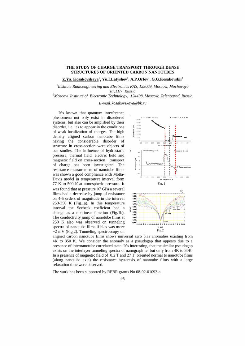
95
5 0 1 0 0 1 5 0 2 0 0 2 5 0 3 0 0 3 5 0 4 0 0 4 5 0
- 1 0
- 5
0
5
1 0
1 5# 2 1 0 S W N T /q u a r t z P r e s s u r e 1 a tm
Ther
mop
ower
, µµ µµV
/К
T e m p e r a tu r e , К
5 0 1 0 0 1 5 0 2 0 0 2 5 0 3 0 0 3 5 0 4 0 0 4 5 0
0
1 0 0 0
2 0 0 0
3 0 0 0
4 0 0 0
5 0 0 0
6 0 0 0
7 0 0 0P r e s s u r e 0 ,7 G P a# 2 1 0 ( S W N T / q u a r t z )
Res
ista
nce
, Oh
m
T e m p e r a tu r e , К
Fig. 1
THE STUDY OF CHARGE TRANSPORT THROUGH DENSE STRUCTURES OF ORIENTED CARBON NANOTUBES
Z.Ya. Kosakovskaya1, Yu.I.Latyshev1, A.P.Orlov1, G.G.Kosakovskii2
1Institute Radioengineering and Electronics RAS, 125009, Moscow, Mochovaya str.11/7, Russia
2Moscow Institute of Electronic Technology, 124498, Moscow, Zelenograd, Russia
E-mail:[email protected]
It’s known that quantum interference phenomena not only exist in disordered systems, but also can be amplified by their disorder, i.e. it's to appear in the conditions of weak localization of charges. The high density aligned carbon nanotube films having the considerable disorder of structure in cross-section were objects of our studies. The influence of hydrostatic pressure, thermal field, electric field and magnetic field on cross-section transport of charge has been investigated. The resistance measurement of nanotube films was shown a good compliance with Motta-Davis model in temperature interval from 77 K to 500 К at atmospheric pressure. It was found that at pressure 07 GPa a several films had a decrease by jump of resistance on 4-5 orders of magnitude in the interval 250-350 К (Fig.1а). In this temperature interval the Seebeck coeficient had a change as a nonlinear function (Fig.1b). The conductivity jump of nanotube films at 250 K also was observed on tunneling spectra of nanotube films if bias was more ~2 mV (Fig.2). Tunneling spectroscopy on aligned carbon nanotube films shows universal zero bias anomalies existing from 4K to 350 K. We consider the anomaly as a pseudogap that appears due to a presence of internanotube correlated state. It’s interesting, that the similar pseudogap exists on the interlayer tunneling spectra of nanographite but only from 4K to 30K. In a presence of magnetic field of 0.2 Т and 27 T oriented normal to nanotube films (along nanotube axis) the resistance hysteresis of nanotube films with a large relaxation time were observed.
The work has been supported by RFBR grants No 08-02-01093-a.
a
b
Fig.2
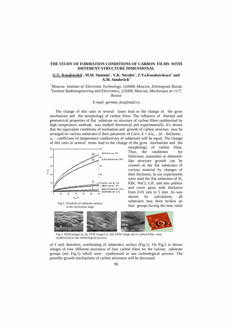
96
THE STUDY OF FORMATION CONDITIONS OF CARBON FILMS WITH DIFFERENT STRUCTURE DIMENSIONAL
G.G. Kosakovskii1, M.M. Simunin1, V.K. Nevolin1, Z.Ya.Kosakovskaya2 and A.M. Smolovich2
1Moscow Institute of Electronic Technology, 124498, Moscow, Zelenograd, Russia 2Institute Radioengineering and Electronics, 125009, Moscow, Mochovaya str.11/7,
Russia
E-mail: [email protected]
The change of this ratio in several times lead to the change of the grow mechanism and the morphology of carbon films. The influence of thermal and geometrical properties of flat substrate on structure of carbon films synthesized by high temperature methods was studied theoretical and experimentally. It's shown that the equivalent conditions of nucleation and growth of carbon structure may be arranged on various substrates if their parameter of Curie k = d/aп , (d – thickness , ап – coefficient of temperature conductivity of substrate) will be equal.The change of this ratio in several times lead to the change of the grow mechanism and the
morphology of carbon films. Thus, the conditions for fullerenes, nanotubes or diamond-like structure growth can be created on the flat substrates of various material by changes of their thickness. In our experiments were used the flat substrates of Si, KBr, NaCl, LiF, and also polikor and cover glass with thickness from 0.01 mm to 5 mm. As was shown by calculation, all substrates may been broken on four groups having the near value
of k and, therefore, overheating of substrate's surface (Fig.1). On Fig.2 is shown images of four different structures of four carbon films for the various substrate groups (see Fig.1) which were synthesized in one technological process. The possible growth mechanisms of carbon structures will be discussed.
Fig.2. SEM images (a, b), STM image (с) and AFM image (d) of carbon films were synthesized in one technological process
100nm Glass
100 nm 1µm
NaClPolycor 200 nm
Si
Fig.1. Overheat of substrate surface at the nucleation stage
97
DYNAMIC KINK STATES IN INTRINSIC JOSEPHSON JUNCTIONS GENERATED BY INTERNAL RESONANCE
A. Koshelev
Materials Science Division, Argonne National Laboratory, USA
Intrinsic Josephson-junction stacks are realized in mesas fabricated out of high-temperature superconductors, such as Bi2Sr2CaCu2O8+x. Phase oscillations in different junctions can be synchronized via coupling to the internal cavity mode leading to powerful electromagnetic radiation in terahertz frequency range [1]. As homogeneous oscillations do not couple directly to the cavity modes, the mechanism of mode excitations is a nontrivial issue. New dynamic state providing a very efficient coupling has been demonstrated recently [2]. A key feature of this state is the alternating phase kinks and antikinks statically located near the center and coexisting with the oscillating phases. We studied evolution of this state with increasing magnetic field at fixed current and found several dynamic regimes. The initial kink state remains stable up to a certain critical field, similar to the lower critical field. Above this field the kink configuration starts to restructure and we observe formation of different static kink lattices existing inside dynamic states. These lattices represent new resonance-stabilized coherent states which differ considerably from the well-known static and moving Josephson vortex lattices. The voltage monotonically increases with the magnetic field and behavior changes when the voltage exceeds the resonance voltage. Above this voltage the kink states become disordered and the voltage-field dependence becomes noisy. Finally, above certain field, the coherence is lost completely and chaotic state emerges. We will also discuss (i) stability analysis of the coherent states and (ii) synchronization regimes in inhomogeneous mesas.
This work was supported by the U. S. DOE, Office of Science, under contract # DE-AC02-06CH11357.
References
[1] L. Ozyuzer et al. , Science 318, 1291 (2007); A. E. Koshelev and L. N. Bulaevskii, Phys. Rev. B 77, 014530 (2008). [2] Sh. Lin and X. Hu, Phys.Rev. Lett., 100, 247006 (2008); A. E. Koshelev, Phys. Rev., B 78, 174509 (2008).
98
ELECTRODYNAMICS AND INTRINSIC JOSEPHSON EFFECTS IN MULTI-GAP SUPERCONDUCTORS
T. Koyama1, Y. Ota2, and M. Machida2
1 IMR, Tohoku University, 2-1-1 Katahira, Sendai 980-8577, Japan 2 CCSE, Japan Atomic Energy Agency, 6-9-3, Higashi Uneno, Tokyo 110-0015
E-mail: [email protected]
The capacitively-coupled intrinsic Josephson junction model [1], which is used for the analysis of the intrinsic Josephson effects observed in highly-anisotropic high-Tc cuprates, is extended to the multi-junction systems composed of 2-gap superconducting layers with an atomic-scale layer thickness. In the 2-gap systems one can define two kinds of superconducting phase-differences between superconducting layers. The coupled dynamical equations for the phase-differences are derived from the effective Lgrangian in this system. We solve numerically the dyanmical equations and calculate the I-V characteristics. The phase-differences in the voltage state depend on the signs of the superconducting gaps (s++ or s+-). We also discuss the effect of the Leggett mode existing in multi-gap superconductors on the dynamics of the phase-differences.
References
[1] T. Koyama and M. Tachiki, I-V characteristics of Josephson-coupled Layered superconductors wit longitudinal plasma excitations. Phys. Rev. B, 54, 16183 (1996)
99
MOBILITY IN EPITAXIAL GaN: LIMITATION OF ELECTRON TRANSPORT DUE TO DISLOCATION WALLS
S.E. Krasavin
Bogoliubov Laboratory of Theoretical Physics, Joint Institute for Nuclear Research, 141980 Dubna, Moscow Region, Russia
A theoretical model to explain the bell-shaped dependence of the mobility versus free carrier concentration n in GaN layers was proposed. The decrease of the total mobility with n decreasing can be obtained in this model by introducing charged dislocation walls as an additional mechanism of scattering. The agreement with experiments for GaN layers was found.
100
THE MAGIC GOLD CLUSTER Au20(TD) AND ITS LOW -ENERGY FULLERENE-TYPE ISOMERS
E.S. Kryachko
Bogilyubov Institute for Theoretical Physics and Department of Chemistry, University of Liege
E-mail: [email protected]
The 20-nanogold cluster Au20 exhibits a large variety of two- and three-dimensional isomeric forms. Among them is the ground-state isomer Au20(Td) representing the stable cluster with a unique tetrahedral shape, with all atoms on the surface, and large HOMO-LUMO gap which even slightly exceeds that of the buckyball fullerene C60. The anionic cluster Au20-(Td) holds its parent tetrahedral symmetry features a high catalytic activity. The list of the properties of the 20-nanogold clusters surveyed in the present work ranges from the energetic order of stability of its isomers to the optical absorption and excitation spectra of the Au20(Td) cluster. We also report the structures and the properties of its doubly charged clusters Au202+ and Au202- and computationally confirm that Au202- is indeed stable. The zero-point-energy-corrected adiabatic second electron affinity of Au20(Td) amounts to 0.43 . 0.53 eV that is consistent with the experimental data. In addition, we provide computational evidence of the existence of the novel, hollow cage isomers of Au20 and analyze their key properties. These 20-nanogold low-energy hollow cages are thoroughly examined: their structures and stabilities, their key properties are revealed and compared with Au20Z(Td) in the different charge states Z=+1,0,-1, and -2. Their void reactivity are investigated at the DFT level. Special attention is devoted to the bifunctional reactivity of the studied Au20 hollow cages, the outer or exo-reactivity and the inner, void, or endo-reactivity. We analyze the general features of the voids of the reported golden fullerenes. The values of ionization potentials and electron affinities, the molecular electrostatic potential and HOMO-LUMO patterns are compared with those of C60 that has a similar void size.
101
NANOSCALE SIZE EFFECTS
A.I. Kuklin 1,2, A.V. Rogachev1,3, A.Yu. Cherny1, T.N. Murugova1, E.B. Dokukin1, O.I. Ivankov1,4, Yu.S. Kovalev1, D.V. Soloviev1,4, P.K.Utrobin2,
A.G. Soloviev1, V.I. Gordeliy1,2,5,6 1Joint Institute for Nuclear Research, Dubna, Moscow reg., Russia,
2Moscow Institute of Physics and Technology, Dolgoprudny , Moscow reg., Russia 3Skobeltsyn Institute of Nuclear Physics of Lomonosov MSU, Moscow, Russia
4Taras Shevchenko Kyiv National University, Kyiv, Ukraine 5IBS,Grenoble, France 6IBS,Julich, Germany
Email: [email protected]
In this report we review various aspects of size effects. By analyizing a series of examples we show that various intensive macroscopic characteristics of nanoobjects exhibit non-trivial size dependencies on the scale from 200 to 40 Å. A method for determining the point of critical changes is suggested. It is shown that drastic variations take place for the sizes in the region 40-60Å for ordinary systems and 120-200 Å in the case of magnetic systems. A connection between the ratio “surface-volume” for nanoparticles and the size effects is discussed.
102
PERSPECTIVES OF SUPERCONDUCTING NANO-ELECTRONICS
F.V. Kusmartsev
Loughborough University, LE11 3TU, Loughborough, UK
E-mail: [email protected]
In the present work we have develped logic gates, that are fundamental structures of digital circuits based of superconducting nano-structures. There are seven basic logic gates (AND, OR, XOR, NOT, NAND, NOR, and XNOR). All other types of Boolean logic gates can be created from a suitable network of just NAND or NOR gate(s). At the present technology logic gates are mostly made of Complementary Metal Oxide Semiconductor transistors and diodes. Often millions or billions of logic gates are packaged in a single integrated circuit. We show that these semiconducting technology can be replaced by superconducting one. Our study is focused on fluxon logic gates which are based on fluxon dynamics. We show that it is possible to produce logic gates based on fluxon dynamics using two dimensional Josephson Transmission Lines and Josephson junctions of various shapes. The logic is based on the flux cloning and fluxon collision phenomena developed recently. We designed OR, AND, XOR and the universal logic gate NAND, estimated they operational times and described simple computing processes with the use of the described fluxon logics.
103
DIRAC FERMIONS IN GRAPHITE NANOSTRUCTURES
Yu.I. Latyshev1, A.P. Orlov1, A.Yu. Latyshev1, W. Escoffier2, P. Monceau3
1Kotelnikov Institute of Radio-Engineering and Electronics RAS, Mokhovaya 11-7, 125009 Moscow, Russia
2National Laboratory of High Magnetic Fields, 143 av. de Rangueil, 31432 Toulouse, France
3Neel Institute, CNRS, 25 av. des Martyrs, 38042 Grenoble, France
E-mail: [email protected]
Discovery of Dirac fermions in graphene renewed the interest to graphite. The existence of Dirac fermions has been established in thin single crystals of graphite as well by magnetooptics [1], STM [2] and interlayer tunneling [3] experiments.
Here we report on our recent experiments on interlayer tunneling in graphite mesa-type structures in high magnetic fields up to 55 T as well as on the experiments on quantum interference of carriers in thin graphite single crystals with columnar defects containing magnetic flux (Aharonov-Bohm effect) [4]. The experiments on nanostructures of both types indicate significant contribution of Dirac fermions to the in-plane and the out-of-plane magnetotransport in graphite.
The work has been done partly in the frame of International Associated Laboratory (LIA) between IREE RAS and Neel Institute CNRS and has been supported by RFBR grants 08-02-01093, 06-02-72551 and RAS programs “Strongly correlated electrons in solid states and structures” and “Physics of new materials and structures”.
References
[1] K. S. Novoselov, A.K. Geim, S.V. Morozov et al., Two-dimensional gas of massless Dirac fermions in graphene. Nature, 438, 197 (2005). [2] M. Orlita, C. Fugeras, G. Martinez et al., Dirac fermions at the H-point of graphite: magneto transmission studies. Phys. Rev. Lett.,. 100, 136403 (2008). [3] G. Li and E. Y. Andrei, Observation of Landau levels of Dirac fermions in graphite. Nature Physics 3, 623 (2007). [4] Yu.I. Latyshev et al., Interlayer transport in the aligned carbon nanotube films and graphite. J. Phys.: Conf. Series, 129, 012032 (2008). [5] Yu.I. Latyshev, A.Yu. Latyshev, A.P. Orlov et al. Field-periodic magnetoresistance oscillations in thin graphite single crystals with columnar defects. JETP Lett., 90, 480 (2009).
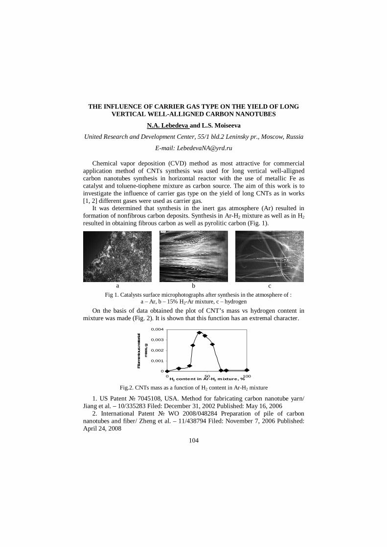
104
THE INFLUENCE OF CARRIER GAS TYPE ON THE YIELD OF L ONG VERTICAL WELL-ALLIGNED CARBON NANOTUBES
N.A. Lebedeva and L.S. Moiseeva
United Research and Development Center, 55/1 bld.2 Leninsky pr., Moscow, Russia
E-mail: [email protected]
Chemical vapor deposition (CVD) method as most attractive for commercial application method of CNTs synthesis was used for long vertical well-alligned carbon nanotubes synthesis in horizontal reactor with the use of metallic Fe as catalyst and toluene-tiophene mixture as carbon source. The aim of this work is to investigate the influence of carrier gas type on the yield of long CNTs as in works [1, 2] different gases were used as carrier gas.
It was determined that synthesis in the inert gas atmosphere (Ar) resulted in formation of nonfibrous carbon deposits. Synthesis in Ar-H2 mixture as well as in H2 resulted in obtaining fibrous carbon as well as pyrolitic carbon (Fig. 1).
a
b
c
Fig 1. Catalysts surface microphotographs after synthesis in the atmosphere of : a – Ar, b – 15% H2-Ar mixture, c – hydrogen
On the basis of data obtained the plot of CNT’s mass vs hydrogen content in mixture was made (Fig. 2). It is shown that this function has an extremal character.
0
0,001
0,002
0,003
0,004
0 50 100H2 content in Ar-H2 mixture, %
Fila
men
tous m
ater
ial
mas
s, g
Fig.2. CNTs mass as a function of H2 content in Ar-H2 mixture
1. US Patent 7045108, USA. Method for fabricating carbon nanotube yarn/ Jiang et al. – 10/335283 Filed: December 31, 2002 Published: May 16, 2006
2. International Patent WO 2008/048284 Preparation of pile of carbon nanotubes and fiber/ Zheng et al. – 11/438794 Filed: November 7, 2006 Published: April 24, 2008
105
COLLECTIVE THERMAL AND QUANTUM DEPINNING OF A ROW O F JOSEPHSON-VORTEX CHAINS IN NATURALLY STACKED HIGH- Tc
JOSEPHSON JUNCTIONS
Gil-Ho Lee, Yong-Duk Jin, and Hu-Jong Lee
Department of Physics, Pohang University of Science and Technology, Pohang, Korea
Email: [email protected]
High-Tc superconducting single crystals of Bi2Sr2CaCu2O8+x (Bi-2212), with high anisotropy, consist of intrinsic Josephson junctions that are inductively coupled along the c axis. Both Josephson vortices (JVs) and pancake vortices (PVs) form in an in-plane and a c-axis magnetic field, respectively. The interaction between Josephson and pancake vortices attracts high interest of current studies. It has been demonstrated that the motion of PVs can be manipulated by the JVs via attractive interaction between them [1-3], which suggests that the JVs can also be controlled by the PVs. A JV behaves as a quantum object, for which the PVs can provide an intrinsic potential wells to implement the vortex-based quantum bits in highly anisotropic superconductors. The flow of rows of JV chains in multiple junctions induces dissipative branches in the tunneling current-voltage characteristics. Each Josephson-vortex-flow branch shows a critical switching current to a neighboring higher-voltage branch. Each switching, caused by depinning of a row of JV chains occurring separately in each junction, is expected to provide very accurate information on the JV dynamics associated with the depinning of JVs from the pinning potential generated by the pancake vortices (PVs) or by the crystal edge. In this study we measured the depinning-current distribution (DCD) with varying temperatures, field strength, and field tilt angles from the in-plane position. The DCD gets much narrowed at sufficiently low temperatures. Below a crossover temperature of 2.5 K, the distribution width is almost saturated and independent of temperature down to 0.38 K, which suggests quantum depinning of JV rows out of the effective pinning potential. In the thermal depinning regime above the thermal-quantum crossover temperature, the PV-induced pinning strength is found to vary with tilting magnetic field angles. This indicates that PVs are the predominating source over the crystal edge for the JV pinning in any small field tilt angles, which is consistent with the results of our previous studies [4].
References:
[1] M. Tokunaga, M. Kobayashi, Y. Tokunaga, and T. Tamegai, Phys. Rev. B 66, 060507 (2002). [2] V. K. Vlasko-Vlasov, A. E. Koshelev, U. Welp, G. W. Crabtree, and K. Kadowaki, Phys. Rev. B 66, 014523 (2002). [3] D. Cole, S. Bending, S. Saveliev, A. Grigorenko, T. Tamegai, and F. Nori, Nat. Mater. 5, 305 (2006). [4] Yong-Duk Jin, Hu-Jong Lee, A. E. Koshelev, Gil-Ho Lee, and Myung-Ho Bae, Europhys. Lett. 88, 27007 (2009).
106
THERMAL STABILITY OF THE PLATONIC HYDROCARBONS AND FULLERENES
K.P. Katin, D.A. Lobanov, M.M. Maslov
National Research Nuclear University “MEPhI” Kashirskoe Sh. 31, Moscow 115409, Russia
E-mail: [email protected], [email protected]
Thermal stability of the small cage clusters known as platonic hydrocarbons (tetrahedrane C4H4 and cubane C8H8) and fullerenes (C20, C36 and C60) was studied over a wide temperature range using tight-binding molecular dynamics simulation with the transferable potential for carbon [1] and nonorthogonal model originally developed for hydrocarbons [2]. Ab initio calculations using HF, MP2 and B3LYP methods with 6-31G* and 6-311G** basis sets were also carried out. We determined structural and thermodynamic properties of the platonic hydrocarbons and fullerenes. Possible channels and final products of their decomposition were also analyzed in detail. Furthermore, temperature dependencies of their lifetimes before decomposition were obtained and the activation energies aE and frequency factors A of the Arrhenius equation were calculated. These values for tetrahedrane and cubane were found to be 0.7 0.1aE = ± eV, 14.52 0.5910A ±= s–1 and
1.9 0.1aE = ± eV, 16.03 0.3610A ±= s–1, respectively. We also calculated the heights of
minimal energy barriers U preventing the decomposition of fullerenes. These averaged values were found to be 4.5; 5.4; 6.9U ≈ eV for C20, C36 and C60 fullerenes, respectively. Note that the activation energies calculated for C20, C36 and C60 fullerenes were found to be 5.5; 6.5; 6.6aE ≈ eV, respectively. The obtained results are essential in optimizing conditions of synthesis of the platonic hydrocarbons, fullerenes and the structures derived from them.
This work was supported by Federal Target Program “Research and Scientific-Pedagogical Cadres of Innovative Russia” for 2009–2013 years (Appl. Number NK-255P; Grant P448 and Appl. Number NK-263P; Grant P1037).
References
[1] C.H. Xu, C.Z. Wang, C.T. Chan, K.M. Ho A transferable tight-binding potential for carbon. J. Phys.: Condens. Matter, 4, 6047–6054 (1992). [2] M.M. Maslov, A.I. Podlivaev, L.A. Openov Nonorthogonal tight-binding model for hydrocarbons. Phys. Lett. A, 373, 1653–1657 (2009).
107
COHERENT PHASES IN GRAPHENE AND GRAPHENE BASED NANOSTRUCTURES
Yu.E. Lozovik
Institute of Spectroscopy, 142190 Troitsk, Moscow Region, Russia
We discuss coherent electronic phases and collective phenomena in graphene and graphene based nanostructures, in particular peculiarities connected with graphene interesting electronic properties similar to ultrarelativistic physics.The collective properties of different types of quasiparticles in graphene is considered: 2D spatially indirect magnetoexcitons in two-layer graphene, magnetoexcitonic polaritons (magnetopolaritons) in a graphene layer embedded in an optical microcavity in a strong magnetic field and 2D indirect magnetobiexcitons in a slab of superlattice of graphene layers. We predict Bose-Einstein condensation (BEC) and superfluidity of indirect magnetoexcitons, indirect magnetobiexcitons and BEC of magnetoexcitonic polaritons in a strong magnetic field. Strongly correlated phases of of magnetoexcitons in bilayer graphene is predicted.
Besides BCS regime strong coupling regime is discussed for e-h pairing in bilayer separately biased graphene layers without magnetic field. The suppression of superfluid density and Kosterlitz-Thouless transition temperature by impurities is considered. The e-h condensation in coupled graphene sheets can be observed through Josephson-like phenomena etc. and can be used as nondissipative nanolectronic element.
Phonons and possible superconductivity in strongly doped graphene are analyzed.
The effective Hamiltonian of the gas of cavity polaritons in a graphene layer in high magnetic field are obtained and the BEC temperature as functions of magnetic field is calculated. A 2D gas of magnetopolaritons is considered in a harmonic potential trap and possible physical realizations of this are discussed.
Plasma oscillations, plasmon polaritons and instabilities in graphene and graphene array are discussed.
Quantum dots, nanotransistors and new type of nanoelements based on graphene are discussed.
The method of calculations of nanoelements based on graphene by generalized density functional approach for system with “ultrarelativistic” electronic spectra are developed. Possible NEMS based on graphene are analyzed.
References
[1] O. L. Berman, Yu. E. Lozovik, G. Gumbs, Bose-Einstein condensation and superfluidity of magnetoexcitons in bilayer graphene, Phys. Rev. B 77, 155433 (2008). [2] O. L. Berman, R. Ya. Kezerashvili, and Yu. E. Lozovik, Collective properties of magnetobiexcitons in quantum wells and graphene superlattices, Phys. Rev. B 78, 035135 (2008)
108
[3] O. L. Berman, R. Ya. Kezerashvili, and Yu. E. Lozovik, Bose-Einstein condensation of trapped polaritons in two-dimensional electron-hole systems in a high magnetic field, Phys. Rev. B 80, 115302 (2009). [4] Yu.E.Lozovik, A.A.Sokolik, Electron-hole pair condensation in graphene bilayer, JETP Lett., 87, 55(2008); Collective electron phenomena in graphene, Physics-Uspekhi, 51, No.7, pp. 727-748 (2008). [5] O.L.Berman, G.Gumbs, Yu.E.Lozovik, Magnetoplasmons in layered graphene structures, Phys.Rev.,B 78, No.8, 085401 (2008 ). [6] O.L. Berman, Yu.E. Lozovik, D.W. Snoke, Theory of Bose-Einstein condensation and superfluidity of two-dimensional polaritons in an in-plane harmonic potential, Phys. Rev. B 77, No.15, 155317 (2008). [7] Yu.E. Lozovik, A.A. Sokolik, M. Willander, Coherent phases and magnetoexcitons in graphene, Physica Status Solidi A 206, 927-930 (2009). [8] Yu.E. Lozovik, S.L. Ogarkov, A.A. Sokolik, Theory of superconductivity of Dirac electrons in graphene, ZhETF, 137, (2010). In print [9] Yu.E. Lozovik, A.A. Sokolik, Multi-band pairing of ultrarelativistic electrons and holes in graphene bilayer, Phys. Lett. A 374, 326-330(2009). [10] Yu.E.Lozovik, Strong correlations and new phases in a system of excitons and polaritons, Physics-Uspekhi, 52, 286 (2009). [11] Yu.E. Lozovik, A.A. Sokolik, Multi-band pairing of ultrarelativistic electrons and holes in graphene bilayer, Phys. Lett. A 374, 326-330(2009). [12] O. L. Berman, R. Ya. Kezerashvili, Yu. E. Lozovik, Bose-Einstein condensation of quasiparticles in graphene, Nanotechnology, (2010). In print.
109
ELECTROMAGNETIC WAVE EMISSION AND REFLECTION IN JOSEPHSON JUNCTIONS; AN ANALYTICAL APPROACH
M. Machida1,3, N. Sasa1,3, T. Koyama2,3, and H. Matsumoto2,3
1CCSE, Japan Atomic Energy Agency, 6-9-3 Higashi-Ueno, Taito-ku Tokyo 110-0015, Japan
2IMR, Tohoku University, 2-2-1 Katahira, Aobaku, Sendai 980-8577, Japan 3CREST(JST), 4-1-8 Honcho, Kawaguchi, Saitama 332-0012, Japan
E-mail: [email protected]
Recently, THz electromagnetic wave emission from intrinsic Josephson junctions has attracted much interest in the research community of Josephson junctions. As a consequence of intensive and extensive experimental and theoretical works on the issue, it has been well-known that both AC Josephson effect and cavity resonance contribute to the large-power THz radiation. However, the electromagnetic-wave radiation mechanism has been not clarified yet, and no reliable proposal to enhance the power and optimize the system has been suggested.
In this paper, we therefore study the electromagnetic wave emission from Josephson junctions in an analytical sense in order to clarify how Josepshon junction radiates electromagnetic wave. For the purpose, we simply concentrate on a standard single junction system as described by sine-Gordon equation and consider a problem of connection between a junction and an external non junction (vacuum) region.
We reveal that a construction of an analytic formula is possible when the elliptic functions are used and the boundary condition is properly considered. Moreover, we discuss what is important and essential for large-power emission based on the formula.
110
DENSITY PROFILES AND INERTIA MOMENTS OF INTERACTING BOSONS IN ANISOTROPIC HARMONIC CONFINEMENT
A.I. Mese1, P. Capuzzi2, Z. Akdeniz3 and S.E. Okan1 1Department of Physics, Trakya University, 22030 Edirne, Turkey
2Consejo Nacional de Investigaciones Cient´ıficas y T´ecnicas and Departamento de F´ısica,FCEyN, Universidad de Buenos Aires, Buenos Aires, RA-1428, Argentina
3Physics Department, Piri Reis University, 34940 Tuzla, Istanbul, Turkey
We investigated the structural properties of a system, consisting of N strongly coupled charged bosonic atoms (Rubidium), moving in two dimensions, and interacting through a repulsive K0 potential [1] inside anisotropic two-dimensional harmonic traps, with N in the range from 4 to 9. Increasing the anisotropy of the confinement potential can drive the system from a two-dimensional 2D to a one-dimensional 1D configuration. After that, we calculated inertia moment depend on the anisotropy parameters and particle numbers.
Our density profiles of the ground state configurations are compared with recent experiments [2] and published numerical results [3,4,5] and we obtained a satisfactory agreement.
References
[1] Nelson D R and Seung H S, Phys. Rev. B, 39 9153, 1989 [2] M Saint Jean and C Guthmann, J. Phys.: Condens. Matter 14 (2002) 13653–13660 [3] A. I. Mese, P Capuzzi, J. Phys.: Condens. Matter 20 , 335222, 2008 [4] S. W. S. Apolinario, B. Partoens, and F. M. Peeters, Physical Review E 72, 046122 2005 [5] Romanovsky I, Yannouleas C and Landman U Phys. Rev.Lett., 93 230405, 2004
111
ULTRAFAST FORMATION OF A RESONANT NANOPLASMA IN DOP ED HELIUM DROPLETS
A. Mikaberidze
Max Planck Institute for the Physics of Complex Systems, Noethnitzer Str. 38, office 2b5, 01187, Dresden, Germany
E-mail: [email protected]
Doping a helium nanodroplet with a tiny xenon cluster of a few atoms only, sparks complete ionization of the droplet at laser intensities below the ionization threshold of helium atoms. As a result, the intrinsically inert and transparent droplet turns into a fast and strong absorber of infrared light. Microscopic calculations reveal a two-step mechanism to be responsible for the dramatic change: Avalanche-like ionization of the helium atoms on a femtosecond time scale, driven by field ionization due to the quickly charged xenon core is followed by resonant absorption enabled by an unusual non-spherical nanoplasma within the droplet [1]. In contrast to the well known resonant absorption during the Coulomb explosion of both homogeneous [2] and composite [3] clusters, the resonance here occurs on an electronic time scale. The effect occurs for an arbitrary elliptical laser polarization. The ellipticity parameter controls the shape of the resulting nanoplasma. Linearly polarized pulses produce a cigar-shaped nanoplasma, while a circular laser polarization gives rise to a pancake-like nanoplasma. Time-dependent observation of the transient nanoplasma shape may be possible with the help of a IR-UV pump-probe scheme.
References
[1] A. Mikaberidze, U. Saalmann, and J. M. Rost, Phys. Rev. Lett. 102, 128102 (2009). [2] U. Saalmann and J. M. Rost, Phys. Rev. Lett. 91, 223401 (2003). [3] A. Mikaberidze, U. Saalmann, and J. M. Rost, Phys. Rev. A 77, 041201(R) (2008).
112
CALCULATION OF ENERGY EIGEN VALUE FOR NANO-WIRES
A.H. Mohammadzaheri1, P. Nooraliei1, A. Ali Zolanvari 2 1P.N.U payame noor university branch of Hammedan, Hamedan, Iran
2Arak university, Arak Iran
In this work we have evaluated eigen value of energy for different cross section of nano wires. We have solved the sherodinger equation by expanded the wave function and using two following approximations. These approximations are "varriating mass effective with position" and "free particle". We consider the hyperbolic function for the first approximation.
The energy eigen values are calculated for Ga-As in square cross section shape and (50*50) nanometer size. Our results are very near the results wich have performed by Gangopadhya.
113
PHYSICAL LIMITS FOR SCALING OF INTREGRATED CIRCUITS
W. Nawrocki
Poznan University of Technology, ul. Piotrowo 3A, 60-965 Poznan, POLAND
E-mail: [email protected]
In this paper we discuss some physical limits for scaling of devices and conducting paths inside of semiconductor integrated circuits (ICs). Since 40 years only a semiconductor technology, mostly the CMOS and the TTL technologies, are used for fabrication of integrated circuits in the industrial scale. Miniaturization of electronic devices in integrated circuits has technological limits and physical limits as well. In 2010 best parameters of commercial ICs shown the dual-core Intel Core i5-670 processor manufactured in the technology of 32 nm. Its clock frequency in turbo mode is 3.73 GHz. A forecast of the development of the semiconductor industry (ITRS 2009) predicts that sizes of electronic devices in ICs circuits will be smaller than 10 nm in the next 10 years. The physical gate length in a MOSFET will even amount 7 nm in the year 2024. At least 5 physical effects should be taken into account if we discuss limits of scaling of integrated circuits.
1. Quantization of both electrical and thermal conductance in narrow and thin transistors` channels and in conducting paths.
2. Spread of doping atoms in a semiconductor material. In a n-doped silicon cube with the size of (10 nm)3 there are 5×10⁴ atoms and 1% chance only to find one free electron. In order to keep the conductive properties of the semiconductor material one should apply more intensive doping, eg. 1020 cm-3. Low number of free electrons should be scattered evenly in whole volume of a material.
3. Electrostatics; a loss of electrostatic control of the drain current in a MOSFET. The channel length LE of Si MOSFET is limited by a degradation of electrostatic control in the transistor. The minimal channel length depends on thickness of channel Hch, thickness of insulation layer Hi, dielectric constants of a channel ε and insulation εi . If we take the ratio εi/ε ≈ 0.3 (for silicon oxide and silicon), thickness of channel Hch = 2 nm, thickness of insulation Hi = 1.5 nm – the estimated minimal length of channel is LE ≈ 3 nm.
4. Electron tunneling between a source and a drain inside a MOSFET through a insulation (oxide). The tunneling effect depends on the channel length L and the supply voltage (drain-source voltage).
5. Propagation time of electromagnetic wave along and across a chip (IC); The new quad-core Intel Core i5-670 processor has a width a = 37.5 mm and a length b = 37.5 mm. The period of the highest clock frequency (3.73 GHz) is Tck = 270 ps. But the propagation time for an electromagnetic wave across a chip is Tp = = 300 ps. According to the state of the art the minimal length of gate in MOSFET in silicon integrated circuits is around 3 nm (thus – technology of 3 nm!). However technological limits allow to apply only the 10 nm-technology in the next 10 years.
114
SPIN-ORBIT EFFECTS IN SEMICONDUCTOR NANOSTRUCTURES IN A MAGNETIC FIELD
R.G. Nazmitdinov1,2, K.N. Pichugin3 1Departament de Fsica, Universitat de les Illes Balears
Palma de Mallorca, Spain 2BLTP, Joint Institute for Nuclear Research, Dubna, Russia
3Kirensky Institute of Physics, Akademgorodok 50/38, 660036, Krasnoyarsk, Russia
E-mail: [email protected]
We analyze the interplay between different spin-orbit (Dresselhaus, Bychkov-Rashba, and Zeeman) interactions in two-dimensional semiconductors under vertical and in-plane magnetic fields. The analysis is done in the effective-mass approximation approach. We obtained an analytical expression for the effective cyclotron frequency that depends on the spin-orbit interactions at the vertical magnetic field [1]. We show that spin precession in a semiconductor quantum wire, caused by the Rashba and the Dresselhaus interactions (both of arbitrary strengths), can be suppressed by means an in-plane magnetic field. Imposing a translational invariance in the longitudinal coordinate, we found a new type of symmetry, which arises at a particular set of intensity and orientation of the magnetic field and explains this suppression [2]. In virtue of this symmetry the spin precession is suppressed at arbitrary polarization of the injected electrons. By setting these conditions 'on' and 'off', the flow of a certain spin polarization through the device is either allowed or destroyed, thus, defining a transistor-like action for the spin. Introducing an additional random potential scV ( 0=⟩⟨ scV ) in the wire, we found that this symmetry is numerically robust even at large potential values :
Fsc EVVar 0.4)( ±≈ , where FE is a Fermi energy of the injected electrons.
References
[1] M. Valn-Rodrguez and R.G. Nazmitdinov, "Model for spin-orbit effects in two-dimensional semiconductors in magnetic fields" Phys. Rev. B 73, 235306 (2006). [2] R.G. Nazmitdinov, K. N. Pichugin, and M. Valn-Rodrguez, "Spin control in semiconductor quantum wires: Rashba and Dresselhaus interaction" Phys. Rev. B, 79, 193303 (2009).
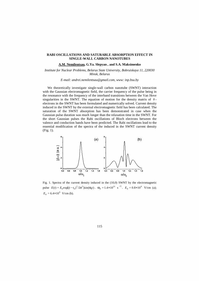
115
RABI OSCILLATIONS AND SATURABLE ABSORPTION EFFECT I N SINGLE-WALL CARBON NANOTUBES
A.M. Nemilentsau, G.Ya. Slepyan , and S.A. Maksimenko
Institute for Nuclear Problems, Belarus State University, Bobruiskaya 11, 220030 Minsk, Belarus
E-mail: [email protected], www: inp.bsu.by
We theoretically investigate single-wall carbon nanotube (SWNT) interaction with the Gaussian electromagnetic field, the carrier frequency of the pulse being in the resonance with the frequency of the interband transitions between the Van Hove singularities in the SWNT. The equation of motion for the density matrix of π -electrons in the SWNT has been formulated and numerically solved. Current density induced in the SWNT by the external electromagnetic field has been calculated. The saturation of the SWNT absorption has been demonstrated in case when the Gaussian pulse duration was much longer than the relaxation time in the SWNT. For the short Gaussian pulses the Rabi oscillations of Bloch electrons between the valence and conduction bands have been predicted. The Rabi oscillations lead to the essential modification of the spectra of the induced in the SWNT current density (Fig. 1).
Fig. 1. Spectra of the current density induced in the (10,0) SWNT by the electromagnetic
pulse )(sin]/2)[(exp=)( 022
00 tttEtE ωσ− . 150 101.4= ×ω s 1− . 6
0 100.8= ×E V/cm (a); 6
0 106.4= ×E V/cm (b).
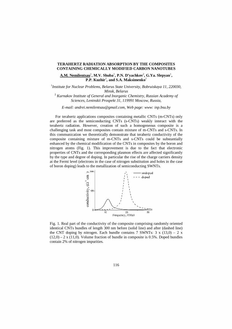
116
TERAHERTZ RADIATION ABSORPTION BY THE COMPOSITES CONTAINING CHEMICALLY MODIFIED CARBON NANOTUBES
A.M. Nemilentsau1, M.V. Shuba1, P.N. D’yachkov2, G.Ya. Slepyan1, P.P. Kuzhir1, and S.A. Maksimenko1
1Institute for Nuclear Problems, Belarus State University, Bobruiskaya 11, 220030, Minsk, Belarus
Kurnakov Institute of General and Inorganic Chemistry, Russian Academy of Sciences, Leninskii Prospekt 31, 119991 Moscow, Russia,
E-mail: [email protected], Web page: www: inp.bsu.by
For terahertz applications composites containing metallic CNTs (m-CNTs) only are preferred as the semiconducting CNTs (s-CNTs) weakly interact with the terahertz radiation. However, creation of such a homogeneous composite is a challenging task and most composites contain mixture of m-CNTs and s-CNTs. In this communication we theoretically demonstrate that terahertz conductivity of the composite containing mixture of m-CNTs and s-CNTs could be substantially enhanced by the chemical modification of the CNTs in composites by the boron and nitrogen atoms (Fig. 1). This improvement is due to the fact that electronic properties of CNTs and the corresponding plasmon effects are affected significantly by the type and degree of doping. In particular the rise of the charge carriers density at the Fermi level (electrons in the case of nitrogen substitution and holes in the case of boron doping) leads to the metallization of semiconducting SWNTs.
Fig. 1. Real part of the conductivity of the composite comprising randomly oriented identical CNTs bundles of length 300 nm before (solid line) and after (dashed line) the CNT doping by nitrogen. Each bundle contains 7 SWNTs: 3 x (13,0) – 2 x (12,0) – 2 x (11,0). Volume fraction of bundle in composite is 0.5%. Doped bundles contain 2% of nitrogen impurities.
117
TRANSPORT OF TRAPPED ATOMS AND CONDENSATES
V.O. Nesterenko1, A.N. Novikov1, A.Yu. Cherny1, and E. Suraud2 1Bogoliubov Laboratory of Theoretical Physics, Joint Institute for Nuclear
Research, Dubna, Moscow region, 141980, Russia 2Laboratoire de Physique Quantique, Universitй Paul Sabatier, 31062 cedex,
Toulouse, France
An irreversible transport of individual atoms and Bose-Einstein condensates (BEC) in multi-well traps is analyzed within the mean field approximation. The transport is driven by time-dependent monitoring the coupling between the wells (barrier penetrabilities) and their relative depth detuning. The particular transfer protocols (Stimulated Rapid Adiabatic Passage, Landau-Zener, mixed Landa-Rozen-Zener) are scrutinized with the accent to most promising adiabatic scenarios [1-3]. It is shown that, while the transfer of individual atoms can be performed quite easily, the transport of BEC meets serious troubles due to the nonlinear effects caused by the interaction between BEC atoms.
In this connection, we propose some effective protocols which overcome this trouble and allow a robust and complete BEC transport in a wide range of both repulsive and attractive interaction [2,3]. Moreover, the non-linearity is turned from detrimental to a favorable transport factor. This opens interesting prospects for manipulating BEC location and creating new dynamical regimes. Besides, since BEC is a coherent system, its transport can be used for generation and investigation of various geometric phases which are now considered as promising information carriers in quantum computing.
References
[1] V.O. Nesterenko, A.N. Novikov, F.F. de Souza Cruz, and E.L. Lapolli, Laser Phys. 19, n.4, 616 (2009). [2] V.O. Nesterenko, A.N. Novikov, A.Yu. Cherny, F.F. de Souza Cruz, and E. Suraud, J. Phys. B. 42, 235303 (2009). [3] V.O. Nesterenko, A.N. Novikov, and E. Suraud, to be published in Laser Phys., 20, n.15, (2010); arXiv:0912.0828[cond-mat.quantum gases].
118
GRAPHENE NANORIBBONS FAR FROM EQUILIBRIUM: FUNDAMENTALS, COMPUTATIONAL ALGORITHMS, AND
NANOELECTRONICS APPLICATIONS
Branislav K. Nikoli ć
Department of Physics & Astronomy and Center for Spintronics & Biodetection, University of Delaware, Newark, DE 19716
[email protected], http://www.physics.udel.edu/~bnikolic
The surprising discovery of graphene, as the first truly two-dimensional crystal where carbon atoms are arranged into a honeycomb lattice, has opened unforeseen avenues for basic research on transport and interactions in low-dimensional electron systems, bench-top testing of quantum electrodynamics, as well as for carbon nanoelectronics. While bulk graphene as a zero gap semiconductor is not suitable for digital electronics applications, the very recent fabrication of sub-10-nm-wide graphene nanoribbons (GNR) could make possible fabrication of complex nanoelectronic circuits from a single graphene sheet or molecular electronics with transparent contacts to conjugated molecules. This also requires substantial first principles quantum transport modeling to capture accurately electronic and atomistic structure of the devices and related charge transfer in equilibrium and charge redistribution under far-from-equilibrium conditions. In this talk, I will review recent advances in the so-called nonequilibrium Green function combined with the density functional theory (NEGF-DFT) approaches that we have utilized to explore: (i) GNR-based nanotransistors composed of thousands of carbon atoms; (ii) nonequilibrium phase transitions between magnetic insulating and non-magnetic metallic phases of GNRs with zigzag edges; (iii) how to employ the spin-dependent shot noise to detect magnetic ordering in GNRs with zigzag edges; and (iv) quantum interference effects in three-terminal GNR-molecule heterojunctions.
References
[1] http://web.physics.udel.edu/research/nanoscale-physics/graphene-nanoelectronics
119
ANOMALOUS NON-EQUILIBRIUM ELECTRON TRANSPORT IN ONE -DIMENSIONAL QUANTUM NANO WIRE AT HALF-FILLING: TIME
DEPENDENT DENSITY MATRIX RENORMALIZATION GROUP STUD Y
M. Okumura 1,2, H. Onishi3, S. Yamada1,2 and M. Machida1,2
1CCSE, Japan Atomic Energy Agency, 6-9-3 Higashi-Ueno, Taito-ku Tokyo 110-0015, Japan
2CREST(JST), 4-1-8 Honcho, Kawaguchi, Saitama 332-0012, Japan 3Advanced Science Research Center, Japan Atomic Energy Agency, Tokai, Ibaraki
319-1195, Japan
E-mail: [email protected]
Recently, photo-induced insulator-metal transition has attracted great attention because of the experimental observation of the surprising ultrafast non-equilibrium phase transition [1-3]. Many theoretical investigations has been continued to understand the mechanism of the ultrafast dynamics during the phase transition [4]. However, all properties of the phase transition have been not fully understood.
In this paper, we study strongly correlated behaviors of electrons at half-filling in a short one-dimensional quantum nano-wire during the photo-pumping via an external electric field by using time-dependent density-matrix renormalization group method. As a result, we observe a very rapid growth of the s-wave superconducting correlation. The superfluid carrier is doublon which is dynamically created by the electric field. We discuss a possibility to observe our results in ultracold atom experiments in near future.
References
[1] S. Iwai, M. Ono, A. Maeda, H. Matsuzaki, H. Kishida, H. Okamoto, and Y. Tokura Ultrafast Optical Switching to a Metallic State by Photoinduced Mott Transition in a Halogen-Bridged Nickel-Chain Compound, Physical Review Letters, 91, 057401 (2003). [2] A. Cavalleri, Th. Dekorsy, H.H.W. Chong, J.C. Kieffer, and R.W. Schoenlein Evidence for a structurally-driven insulator-to-metal transition in VO2: A view from the ultrafast timescale, Physical Review B, 70, 161102(R) (2004). [3] H. Okamoto, H. Matsuzaki, T. Wakabayashi, Y. Takahashi, and T. Hasegawa Photoinduced Metallic State Mediated by Spin-Charge Separation in a One-Dimensional Organic Mott Insulator, Physical Review Letters, 98, 037401 (2007). [4] See for recent developments in theoretical study, e.g., N. Tsuji, T. Oka, and H. Aoki, Nonequilibrium Steady State of Photoexcited Correlated Electrons in the Presence of Dissipation, Physical Review Letters, 103, 047403 (2009).
120
THEORY OF JOSEPHSON EFFECTS IN IRON-BASED MULTI-GAP SUPERCONDUCTOR JUNCTIONS
Y. Ota1,3 , M. Machida1,3,4, and T. Koyama2,3 1 CCSE, Japan Atomic Energy Agency, 6-9-3 Higashi-Ueno, Taito-ku, Tokyo, 110-
0015, Japan 2 Institute for Materials Research, Tohoku University, 2-1-1 Katahira Aoba-ku,
Sendai, 980-8577, Japan 3 CREST(JST), 4-1-8 Honcho, Kawaguchi Saitama, 332-0012, Japan
4 JST-TRIP, 5 Sambancho Chiyoda-ku, Tokyo, 102-0075, Japan
E-mail: [email protected]
Since the discovery of iron-based superconductors [1], Josephson junctions including such new materials have been intensively studied in order to explore their pairing symmetry and application potential. Recently, various types of iron-based superconductor junctions are successfully fabricated. One of interesting features of this type of materials is the presence of multiple (more than two) bands on Fermi surface and their contributions to superconductivity. As a result, iron-based superconductor junctions are possible to have multiple tunneling channels between the superconducting electrodes and relative charge fluctuations between the bands in each electrode. It is an urgent task to reveal how such multi-channel properties affect basic Josephson effects. In the present paper, we show a theory of Josephson junctions with multi-gap superconductors (i.e., multiple tunneling Josephson junctions). We mainly examine a heterotic (multi-band)superconductor- insulator-(single-band)superconductor junction [2]. Deriving an effective Lagrangian density based on the time-dependent Ginzburg-Landau model, we discuss how the relative fluctuations between multiple gaps (i.e., Leggett's collective excitation modes) and the pairing symmetry modify the Shapiro steps, e.g., the step height pattern and the step position.
References
[1] Y. Kamihara, T. Watanabe, M. Hirano, H. Hosono, Iron-based layered superconductor FeAsFOLa xx ][ 1− ( 0.05,0.12=x ) with KTc 26= , J. Am. Chem. Soc. 130 3296 (2008). [2] Y. Ota, M. Machida, T. Koyama, and H. Mastumoto, Theory of heterotic superconductor-insulator-superconductor Josephson junctions between single- and multiple-Gap superconductors, Phys. Rev. Lett. 102, 237003 (2009).
121
FINE SPECTRAL FEATURES IN TERAHERTZ WAVE EMITTING Bi2Sr2CaCu2O8+d MESAS
L. Ozyuzer1, F. Turkoglu1, H. Koseoglu1, Y. Demirhan1, Z. Meric1, Y. Simsek2,
C. Kurter 3, U. Welp3, K. E. Gray3, T. Yamamoto4, K. Kadowaki4,
H.B. Wang5, P. Müller2 1Department of Physics, Izmir Institute of Technology, Urla 35430, Izmir, Turkey
2Phys. Inst. III, University of Erlangen-Nurnberg, Germany 3Materials Science Division, Argonne National Laboratory, Illinois, USA
4University of Tsukuba, Tsukuba, Japan 5National Institute for Materials Science, Tsukuba, Japan
E-mail: [email protected]
Josephson Junctions are the simplest voltage to high frequency converters which can be used as a solid state source of terahertz radiation. Since terahertz waves is an important tool across the physical, chemical and biological sciences, the search is continuing for reliable coherent, continuous, tunable and compact solid-state sources. Although Josephson junctions are potential candidate, the mechanism of powerful terahertz emission from intrinsic Josephson junctions of layered high temperature superconductor Bi2Sr2CaCu2O8+d (Bi2212) mesas is still unresolved. It is shown that the emission frequency is related to mesa width which implies cavity resonance. On the other hand, how synchronization establishes between layers has to be determined. Large area mesas ranging from 100x300 to 40x300 um2 with various heights were formed on Bi2212. Current-voltage (I-V) and THz emission characteristics were obtained at various temperatures. Detailed examination of I-V curves indicated that there are messenger bumps in return branch just before the THz emission. These spectral features are more robust in low frequency mesas. Furthermore, the spectral features in I-V curves were investigated to find a correlation between emission frequency and feature energy. Recent THz experiments on mesas with various geometries and fabrication techniques will also be discussed.
This research is partially supported by TUBITAK (Scientific and Technical Research Council of Turkey) project number 108T238. L.O. acknowledges support from Alexander von Humboldt Foundation.
122
THE EFFECT OF THE ORIENTATION OF STONE-WALES DEFECT S ON THE NONLINEAR CONDUCTANCE OF CARBON NANOTUBES
Pouya Partovi-Azar and Afshin Namiranian
Department of Nano-Science, Institute for Research in Fundamental Sciences (IPM), Computational Physical Science Laboratory, P.O. Box 19395, Tehran, Iran
We study the effect of the orientation of stone-wales (SW) structural defects on the quantum conductance of finite-length single-wall carbon nanotubes (CNT) in the framework of density functional theory using pseudo-atomic orbitals (PAO) basis set. SW defects can occur in different distinct orientation which are the rotated copies of one another by angle /3π around an axis perpendicular to the tube axis. In the case of one single SW defect, the position of the formation of the defect along the circumference of the tube would be unimportant due to the rotational symmetry along the circumference. Our formalism is based on a perturbative scheme within the linear response regime. The correction to the conductance induced by the defects is sensitively dependent on the wavefunction amplitudes of contributing electronic states, the bandsturcture near the Fermi level and the orientation of the defect. These dependencies are systematically studied with the primary focus on the orientation of SW defect.
123
“INTEGRAL” AND “DIFFERENTIAL” CHEMICAL POTENTIALS AND THEIR ROLE IN THE THEORY OF PHASE TRANSITIONS IN AT OMIC
CLUSTERS
V.A. Pavlov
St.-Petersburg State University, Ulianovskaya str. 1, Petrodvorets, St.-Petersburg, 198504 Russia
E-mail: [email protected]
Basic equations of conventional thermodynamics are as follows [1]: dNpdVTdSdE µ+−= , (1)
NpVTSE µ+−= .
In the exact equations of nanothermodynamics [2] the last formula gets complicated:
WNpVTSE +µ+−= . (2)
In a first approximation W ~ A, where A is the square of the cluster boundary. When N → ∞ (macroscopic systems) W = o(N), the value W can be neglected.
In nanothermodynamics there are two chemical potentials, the “integral” µ and
the “differential” µ (see their definitions in book [2] and article [3]). According to formulae (1)–(2) the distinction between the potentials µ and µ is connected with a nonzero value of W [2, 3].
Using the values applying to the equimolecular surface, the surface tension σ and the radiusr , one receives (see [3])
∂σ∂−σ
ρ=µ−µ
rr
m0ˆ . (3)
where m0 is the mass of a molecular and ρ is the nanocluster density. There are results of the exact formula (3) discussed here. In particular, the
ordinary triple point (the equilibrium of three phases) does not exist in nanosystems (see the article [4]). In addition, two effects are known: firstly, the nonzero value of W means that the shift in the melting temperature of a cluster becomes 1,5 times greater; secondly, the pressure of saturated vapor over a liquid nanocluster at the melting point will be considerably greater than the pressure over the solid nanocluster of the same mass (see [3]).
References [1] Landau L. D., Lifshitz E. M. Statistical Physics (Moscow, 2001). [2] Hill T. L. Thermodynamics of Small System. (New York, 1963). [3] Pavlov V. A. Use of the small systems thermodynamics in the theory of nanoparticle melting. Vestnik of the St.-Petersburg University. Ser. 4 (Physics, Chemistry), 2007 (3), 70–74. In Russian. [4] Pavlov V. A. The effect of nanothermodynamics on the phase diagram in the vicinity of the liquid-crystal transition. Vestnik of the St.-Petersburg University. Ser. 4 (Physics, Chemistry), 2009 (3), 132–135. In Russian.
124
CONTROL OF NANOSCALE OPEN QUANTUM SYSTEMS
A.N. Pechen
Chemistry Department, Princeton University, Princeton, NJ 08544, USA
E-mail: [email protected], Web page: http://www.princeton.edu/ apechen/
Nanoscale systems in many situations exhibit quantum features. Examples include electrons in quantum dots, superconducting quantum interference devices, electron and spin transport, quantum rings and wires, etc. Commonly, quantum systems in these and multiple other examples are open and interacting with their environment. Various related to these systems phenomena include seeking an optimal control to maximize an objective or to optimize certain properties of the involved nanoscale systems. Such phenomena can be formulated as control problems for open quantum systems and their analysis can be performed using tools from control theory. This talk will outline certain key topics in control of open quantum systems, including formulations with laser induced coherent control, novel suggestions for environmently induced incoherent control [1], discussion of the degree of controllability [2], and discussion of the practically important property of absence of local maxima and minima for a wide class of objective functions [3,4].
References
[1] A. Pechen and H. Rabitz, Teaching the environment to control quantum systems. Phys. Rev. A, 73, 062102 (2006) [2] R. Wu, A. Pechen, C. Brif and H. Rabitz, Controllability of open quantum systems with Kraus-map dynamics. J. Phys. A: Math. Theor., 40, 5681--5693 (2007) [3] A. Pechen, D. Prokhorenko, R. Wu and H. Rabitz, Control landscapes for two-level open quantum systems. J. Phys. A: Math. Theor., 41, 045205 (2008) [4] R. Wu, A. Pechen, H. Rabitz, M. Hsieh and B. Tsou, Control landscapes for observable preparation with open quantum systems. J. Math. Phys., 49, 022108 (2008)
125
SUPPRESSION OF SPIN-PRECESSION DUE TO RASHBA AND DRESSELHAUS SPIN-ORBIT INTERACTION
BY IN-PLANE MAGNETIC FIELD
R.G. Nazmitdinov1,2 and K.N. Pichugin 3
1 Universitat de les Illes Balears, E-07122 Palma de Mallorca, Spain 2 BLTP, Joint Institute for Nuclear Research, Dubna, Russia
3 Kirensky Institute of Physics, Akademgorodok 50/38, 660036 Krasnoyarsk, Russia
E-mail: [email protected]
We show that spin precession in a semiconductor quantum wire, caused by the Rashba and the Dresselhaus interactions (both of arbitrary strengths), can be suppressed by dint of an in-plane magnetic field. Using a condition of the translational invariance in the longitudinal coordinate, we found a new type of symmetry, which arises at a particular set of intensity and orientation of the magnetic field and explains this suppression. Introducing an additional scattering potential VSC with ⟨ VSC⟩ = 0 in the wire, we found that this symmetry is numerically robust even at a relatively strong scattering potential (Var(VSC) ≈ 0.4EF, where EF is a Fermi energy of the injected electrons). Based on our findings, we propose a transport experiment to measure the strengths of the Rashba and the Dresselhaus interactions.
References
[1] R.G. Nazmitdinov, K. N. Pichugin, and M. Valn-Rodrguez, Spin control in semiconductor quantum wires: Rashba and Dresselhaus interaction Phys. Rev. B, 79, 193303-4 (2009).
126
INFLUENCE OF THE MAGNETIC FIELD ON THE ELECTRONIC SPECTRA OF DOUBLE-WALL CARBON NANOTUBE
M. Pudlak1, R. Pincak1,2 1Institute of Experimental Physics, Slovak Academy of Sciences, Watsonova 47,
043 53 Kosice, Slovak Republic 2Joint Institute for Nuclear Research, BLTP, 141980 Dubna, Moscow region, Russia
E-mail: [email protected]
We study the electronic spectra of double walled carbon nanotube (DWN) influenced by the external magnetic field. We choose the orientation of the magnetic field parallel to the axis of nanotube. We found the strong change of the electronic spectra due to external magnetic field. That means gap between valence and conductive bands in DWN will be changed.
127
SUB-POISSONIAN PHONONIC POPULATIONS IN A NANOELECTROMECHANICAL SYSTEM
F. Cavaliere1 , G. Piovano1 , F. Haupt 2 , M. Merlo 3 , E Paladino4 and
M. Sassetti1
1 Dipartimento di Fisica, Universitа di Genova, LAMIA CNR–INFM, Via Dodecaneso 33, 16146 Genova, Italy
2 University of Konstanz, Fachbereich Physik M703, D-78457, Germany 3 Istituto Nazionale di Fisica Nucleare – Sez. Genova, and Dipartimento di Fisica,
Universitа di Genova, Via Dodecaneso 33, 16146 Genova, Italy 4 MATIS CNR-INFM, Catania & Dipartimento di Metodologie Fisiche e Chimiche,
Universitа di Catania, 95125 Catania, Italy
E-mail: [email protected]
We study the phonon distributions of a mechanical resonator coupled to a single-electron transistor (SET) in the sequential tunneling regime exploiting a master equation approach. In the case of fast vibrations (rotating wave approximation), we show that the electrical current flowing through the SET can induce a out-of-equilibrium distribution of phonons with sub-Poissonian statistics, which is characterized by a selective population of few phonon states [1]. In selected regimes of bias and gate voltages, the selective phonon population is reinforced by the double-occupancy of the SET, allowed when a finite electron-electron interaction is considered [2]. We conclude with some perspective on the regime of slow vibrational motion, where coherences between vibrational states may not be neglected and the rotating wave approximation is dropped in favour of the solution of a generalized master equation exploiting the fully coherent dynamics of the SET+oscillator system [2].
References
[1] M. Merlo, F. Haupt, F. Cavaliere, and M. Sassetti, Sub-Poissonian phononic population in a nanoelectromechanical system New J. Phys. 10, 023008 (2008) Bibliograpy [2] F. Cavaliere, G. Piovano, E. Paladino, and M. Sassetti, Phonon distributions of a single-bath mode coupled to a quantum dot New J. Phys. 10 115004 (2008)
128
OXYGEN ADSORPTION IN CARBON NANOTUBES
V.E.Egorushkin, N.V. Melnikova, A.N. Ponomarev
Institute of Strength Physics and Materials Science, Siberian Division, Russian Academy of Sciences
E-mail: [email protected]
Gas adsorption in carbon nanotubes (CNTs) strongly influences on electron properties of these systems especially in the case of oxygen. The most interesting phenomenon is the temperature behavior of thermopower of the CNTs when one and the same sample in the oxygenated and deoxygenated states has thermopower with opposite sign [1]. Oxygen adsorption in CNTs may be described by the model [5] where electrons of valence band are considered instead of d-electrons of transition metals. We observed that the decay of electron states at the initial stage of oxygen adsorption in CNTs does not play a decisive role and dissociation of oxygen molecules takes place as a result of a sharp enhancement of the vibrational mode of molecules in the mixed state. This enhancement is caused by the resonance between the frequency of natural oscillations (the hybridization energy) and the driving frequency equal to the frequency of transitions between the oxygen molecular levels and the valence band states of electrons of CNTs. These frequencies and the Fermi level position determine the dissociation barrier. In the absence of the resonance, the dissociation does not take place and oxygen can adsorb and exist on the surface of CNTs. In this case the temperature dependence of thermopower of CNTs in the oxygenated and deoxygenated states is well described in the frame of our model [3].
References
[1] K. Bradley et al., Is the Intrinsic Thermoelectric Power of Carbon Nanotubes Positive? Phys. Rev Lett, 85, 4361 - 4364 (2000) [2] V.E. Egorushkin, S.E. Kul’kova, N.V. Mel’nikova and A.N. Ponomarev. To the quantum theory of chemical activity of the surface of transition metals. JETP, 128, 403-410 (2005) [3] V.E. Egorushkin, N.V. Melnikova and A.N. Ponomarev. The role of structural inhomogeneities in the temperature behavior of the thermopower in metallized nanotubes with impurities. Russian Physics Journal, 52, 3, 252-264 (2009)
129
EFFICIENT SPIN PROJECTION IN HARTREE-FOCK CALCULATIO NS
M. Pons and A. Puente
Departament de Fsica, Universitat de les Illes Balears. Palma de Mallorca, Spain.
E-mail: [email protected], [email protected]
In the last years both Hartree-Fock (HF) and density functional theory (DFT) have been extensively applied to study different properties in a variety of electronic nanostructures with occupations that range from moderate to large number of electrons, for which more exact methods, such as exact diagonalization, Quantum Monte Carlo or Configuration Interaction, are not feasible. The importance of correlations in circular quantum dots depends on the so called Wigner parameter (RW), which is a mesure of the relative strength between electron-electron interaction and external confinement. A common drawback in all mean field calculations lies in
the failure to work with good total spin states, i.e. eigenstates of the 2S operator. Spin symmetry, as well as rotational symmetry (for unrestricted HF), restoration methods have proved to be a valuable technique, which led to improved energy estimates and at the same time is able to provide predictions for total spin and angular momentum [1].
In this work we concentrate on the symmetry restoration technique [2], based on the evaluation of the spin projection operator acting on a Slater Determinant (SD) with the help of the Sanibel coefficients [3]. The spin eigenstate is simply expressed as a linear combination of a big new set of SD's obtained by performing all possible spin-exchange operations over the initial state. This state can then be used to estimate different physical quantities through the calculation of appropriate expectation values. We present highly efficient expressions both for the spin decomposition of a single SD and for the expectation values of arbitrary spin-independent one- and two-body operators.
We apply this formalism to circularly confined quantum dots, described within HF, and show how the corresponding expectation values for the total energy and several other observables can be efficiently computed for an arbitrarily large number of electrons. The predictions for the total spin projection (S,SZ) corresponding to the ground state configurations are discussed as a function of RW and the strength of a vertically applied magnetic field. The projected total energies are also compared with their HF counterparts.
References
[1] C. Yannouleas and U. Landman, Rep. Prog. Phys. 70, 2067--2148 (2007) [2] P.-O. Lцwdin, Phys. Rev. 97, 1509--1520 (1955) [3] V.H. Smith and F.E. Harris, J.Math. Phys. 10, 771--778 (1969)
130
MODEL OF FLUID FLOW IN NANOTUBE: CLASSICAL AND QUANT UM FEATURES
I.Yu. Popov1, S.A.Chivilikhin 1 , V.V.Gusarov2 and I.V.Blinova1
1St.-Petersburg State University of Information Technologies, Mechanics and Optics, Kronverkskii, 49, St.-Petersburg, 197101, Russia
2St.-Petersburg State Technological Institute (Technical University), Moskovskii, 26, St.-Petersburg, 190000, Russia
E-mail: [email protected]
Different applications of nanostructures are related with fluid flows through these systems. In its turn, experiments show that flows in nanostructures have many specific features, which can’t be explained in classical terms only. Particularly, flow through nanotube is extremely fast in comparison with its classical analog. We suggest a model based on the possibility of existence of molecular clusters (Frenkel crystallites) in the fluid [1]. There are some experimental evidences of such phenomenon. Under this assumption one needs to take into account quantum effects. Particularly, the boundary condition, which plays the crucial role for the flow in nanostructures, takes the form of sliding condition instead of the adhesion condition for the classical flow. The parameters of the boundary conditions are determined by solving of quantum scattering problem for the particle of the fluid and the wall potential. Main features of the flow are described in the framework of the model. For very narrow nanotubes another phenomena have an influence on the flow- possibility of existence of solitons in nanotube walls. These soliton solutions are similar to Davidov solitons in molecular chains. This model of flow is also described.
References
[1] S.A.Chivilikhin, V.V.Gusarov, I.Yu.Popov, A.I.Svitenkov Model of fluid flow in a nano-channel. Russian J. of Math. Phys., 15 (3), 410-412 (2008)
131
INTERACTION EFFECTS IN QUANTUM DOTS IN A MAGNETIC F IELD
A. Puente1 , M. Pons1 and R.G. Nazmitdinov1,2
1Departament de Fsica, Universitat de les Illes Balears. Palma de Mallorca, Spain 2 Bogoliubov Laboratory of Theoretical Physics, JINR, Dubna, Russia.
E-mail: [email protected]
Quantum dots (QDs) have drawn a great deal of experimental and theoretical attention in recent years. In particular, this interest is due to the fact that QDs may provide a natural realization of quantum bit. It is also related to fundamental aspects of strongly correlated finite systems, which are different from bulk and can be controlled experimentally [1].
A convenient starting point to treat finite systems is, in many cases, a mean field description like the Hartree-Fock (HF) approach [2,3]. Selfconsistency between the mean field and the single-particle orbitals and total energy minimization are the basic conditions at this level. However, the total energy minimization procedure being of nonlinear nature is still a real challenge for many-body quantum theory. Using a two-dimensional parabolic approximation for confining potential in a closed quantum dot, various approaches including ab initio calculations within diffusion and path integral Monte Carlo methods, Hartree-Fock and spin-density functional methods have been applied with some degree of success to analyze the ground state energies of N-electron QDs [1]. Recently we developed an efficient, numerically stable HF procedure and compare our results with available ones in the literature. We demonstrate that our approach superseds many computational procedures.
Based on our procedure, we show that the magnetic field gives rise to dynamical symmetries of N-electron QDs (N ≤ 20) for realistic values of the Coulomb interaction-confinement ratio RW (cf [2,3]). These symmetries manifest themselves as near-degeneracies in the quantum spectrum at specific values of the magnetic field and produce maxima in the addition spectra for specific electron numbers.
Varying the ratio of RW and the strength of the magnetic field we discuss the evolution of the quantum dot geometry, formed in the ground state, from N = 2 to N = 20 electrons.
References
[1] S. M. Reimann and M. Manninen, Rev Mod Phys 74, 1283--1342 (2002) [2] A. Puente, Ll. Serra, and R. G. Nazmitdinov, Phys Rev B 69, 125315(9) (2004) [3] R. G. Nazmitdinov and A. Puente, Int J Mod Phys E 18, 1014--1021 (2009)
132
PECULIARITIES OF PHASE DYNAMICS OF COUPLED JOSEPHSON JUNCTIONS IN CCJJ AND CCJJ+DC MODELS
Y.M Shukrinov 1,2, I.R. Rahmonov1,2, and M. El Demery1,3
1 Joint Institute for Nuclear Research, BLTP, Dubna, Russia 2 Physical Technical Institute, Dushanbe, Tajikistan
3 ECTP, Modern University, Mokattum, Cairo, Egypt
E-mail: [email protected]
[keywords] intrinsic Josephson junctions, phase dynamics, CCJJ model, CCJJ+DC model, current voltage characteristics, breakpoint, longitudinal plasma wave.
The phase dynamics of the coupled Josephson junctions in the framework of CCJJ [1] and CCJJ+DC [2,3] models is studied. The current voltage characteristics (CVC) are numerically calculated for the stacks with different number of junctions at different model parameters. We manifest the difference of these models for the branching at I = Ic and in the hysteretic region. The essential difference is observed in the breakpoint region, where the longitudinal plasma wave is created. To find the origin of the CVC features in the breakpoint region [4,5], we simulate the time dependence of the charge in superconducting layers and demonstrate that its features related to the features in CVC. We discuss the main features of both models, and establish the role of the diffusion current between the superconducting layers. The charge-charge and current-current correlations [6] in the system of coupled Josephson junctions are investigated.
This work was supported by the Russian Foundation for Basic Research under Grant 08-02-00520-a.
References
[1] T. Koyama and M. Tachiki, Phys. Rev. B, 54, 16183 (1996) [2] M. Machida, T. Koyama, A. Tanaka and M. Tachiki, Physica C, 331, 85 (2000) [3] Yu. M. Shukrinov, F. Mahfouzi and P. Seidel, Physica C, 449,62 (2006) [4] Yu. M. Shukrinov and F. Mahfouzi. Phys.Rev.Let., 98, 157001 (2007) [5] Yu. M. Shukrinov, F. Mahfouzi and M. Suzuki, Phys. Rev. B, 78, 134521 (2008) [6] Yu. M. Shukrinov, M. Hamdipour and M. R. Kolahchi. Phys.Rev.B, 80,014512 (2009)
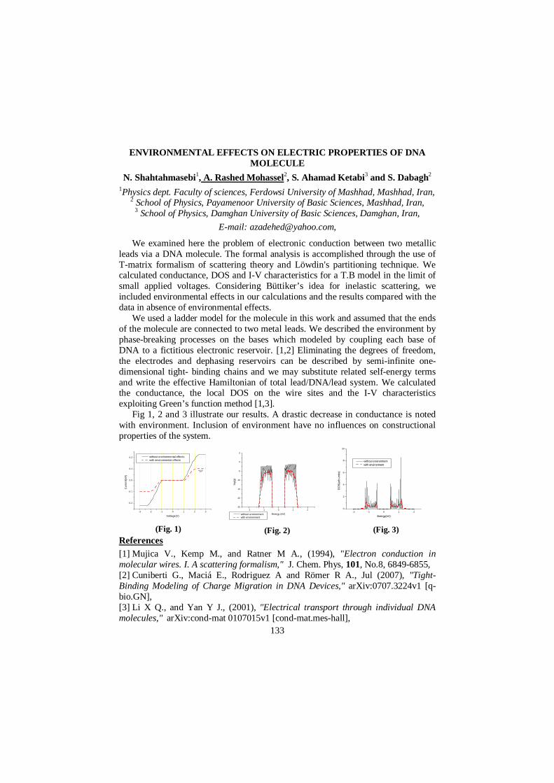
133
-2 -1 0 1 20
2
4
6
8
10
DO
S(a
rb.u
nits
)
Energy(eV)
without environment with environment
ENVIRONMENTAL EFFECTS ON ELECTRIC PROPERTIES OF DNA MOLECULE
N. Shahtahmasebi1, A. Rashed Mohassel2, S. Ahamad Ketabi3 and S. Dabagh2 1Physics dept. Faculty of sciences, Ferdowsi University of Mashhad, Mashhad, Iran,
2 School of Physics, Payamenoor University of Basic Sciences, Mashhad, Iran, 3 School of Physics, Damghan University of Basic Sciences, Damghan, Iran,
E-mail: [email protected],
We examined here the problem of electronic conduction between two metallic leads via a DNA molecule. The formal analysis is accomplished through the use of T-matrix formalism of scattering theory and Löwdin's partitioning technique. We calculated conductance, DOS and I-V characteristics for a T.B model in the limit of small applied voltages. Considering Büttiker’s idea for inelastic scattering, we included environmental effects in our calculations and the results compared with the data in absence of environmental effects.
We used a ladder model for the molecule in this work and assumed that the ends of the molecule are connected to two metal leads. We described the environment by phase-breaking processes on the bases which modeled by coupling each base of DNA to a fictitious electronic reservoir. [1,2] Eliminating the degrees of freedom, the electrodes and dephasing reservoirs can be described by semi-infinite one-dimensional tight- binding chains and we may substitute related self-energy terms and write the effective Hamiltonian of total lead/DNA/lead system. We calculated the conductance, the local DOS on the wire sites and the I-V characteristics exploiting Green’s function method [1,3].
Fig 1, 2 and 3 illustrate our results. A drastic decrease in conductance is noted with environment. Inclusion of environment have no influences on constructional properties of the system.
(Fig. 1) (Fig. 2) (Fig. 3) References [1] Mujica V., Kemp M., and Ratner M A., (1994), "Electron conduction in molecular wires. I. A scattering formalism," J. Chem. Phys, 101, No.8, 6849-6855, [2] Cuniberti G., Maciá E., Rodriguez A and Römer R A., Jul (2007), "Tight-Binding Modeling of Charge Migration in DNA Devices," arXiv:0707.3224v1 [q-bio.GN], [3] Li X Q., and Yan Y J., (2001), "Electrical transport through individual DNA molecules,"arXiv:cond-mat 0107015v1 [cond-mat.mes-hall],
-3 -2 -1 0 1 2 3
-0.2
-0.1
0.0
0.1
0.2
*10-1
Cur
rent
(nA
)
Voltage(V)
without environmental effects with environmental effects
-2 -1 0 1 2-25
-20
-15
-10
-5
0
5
log(
g)
Energy (eV) without environment with environment
134
CLUSTERS IN CONTACT WITH SUBSTRATES - THE EFFECT OF THE INTERFACE ON CLUSTER DYNAMICS
P.-G. Reinhard1, B. Faber1, P. Wopperer1, P.M. Dinh2, and E. Suraud2 1Institut für Theoretische Physik, Universität Erlangen, Staudstr. 7, D-90158
Erlangen, Germany 2Laboratoire de Physique Quantique, Universite Paul Sabatier, 118 Route de
Narbonne, F-31062 Toulouse Cedex, France
The talk presents theoretical studies of coupled ionic and electronic dynamics of metal clusters in contact with an inert environment (insulator substrates as rare gases or MgO) and compares it with the behavior of free clusters. The theoretical tool for these investigations is time-dependent density-functional theory at the level of the local-density approximation. The scheme includes a self-interaction correction to describe properly electron emission. The treatment resolves the fully detailed electronic dynamics at femtosecond scale and proceeds up to several picoseconds to track the consequences on the slow ionic and atomic motion in these complex compounds.
Observable signatures from various dynamical scenarios are discussed. As a basic feature we consider optical response and its modification through the environment. In the non-linear regime, we will consider the dynamics of cluster deposition and excitation by short laser pulses. For embedded and deposited clusters, there emerges the particularly interesting question of energy and particle transport from the highly excited cluster (acting as chromophore) to the inert environment. The various transport processes and corresponding time scales will be analyzed. We will also address the remarkable difference in the dynamics of free clusters and clusters embedded in rare-gas matrix.
135
ANOMALOUS THERMAL CONDUCTIVITY IN MULTIWALLED CARBON NANOTUBES WITH IMPURITIES
V.E. Egorushkin, N.V. Melnikova, A.N. Ponomarev and A.A. Reshetnyak
Institute of Strength Physics and Materials Science, Siberian Division, Russian Academy of Sciences, 634021, Tomsk, Russia
E-mail: [email protected]
The thermal conductivity of nanometer materials plays an important role in controlling the performance and stability of nano/micro devices. The synthesized multiwalled carbon nanotubes (CNT) (to be considered as the perspective elements for those devices) contain in sufficient manner the impurities of metallic catalysts, amorphous carbon and defects (like vacancy, pair of vacancies, adatoms) which significantly influence on peculiarities of electronic and heat transports [1]. In case of bulk disordered CNTs the basic contribution into thermal conductance in the temperature interval near the room temperature is determined by its phonon subsystem (see, for instance [2]). At the same time for a low-temperature region (< 50K) the crucial role both for thermopower and for thermal conductivity belongs to their electronic subsystem [3]. We study the process of heat transport and evaluate the thermal conductivity k(T) in dependence on temperature for the multiwalled CNT with impurities on a base of Green’s functions method, by means of the quantum kinetic Keldysh equation for 3D system and approximation of the transport relaxation time τ , which, in turn, corresponds to an appearance of local order like to amorphous metals.
References
[1] V.E. Egorushkin, S.E. Kul'kova, N.V. Mel'nikova and A.N. Ponomarev, To the quantum theory of chemical activity of the surface of transition metals. JETP, V.128, 403-410 (2005). [2] G. Stoltz, M. Lazzeri and F. Mauri, Thermal transport in isotopically disordered carbon nanotubes: a comparison between Green’s functions and Boltzmann approaches. J. Phys.: Condens. Matter V.21, 245302-01--245302-11 (2009). [3] V.E. Egorushkin, N.V. Mel'nikova and A.N. Ponomarev, The role of structural inhomogeneities in the temperature behavior of the thermopower in metallized nanotubes with impurities. Russian Physics Journal, V.52, 252-264 (2009).
136
MAGNETIC PROPERTIES OF TRANSITION METALS (3D) ADD ON GRAPHENE: A DENSITY FUNCTIONAL STUDY
Mahdi Sargolzaei1,2 and Farideh Gudarzi1
1Department of Physics, Iran University of Science and Technology, Narmak
16345, Tehran, Iran. 2
Computational Physical Science Laboratory, Department of Nano-Science, Institute for Research in Fundamental Sciences (IPM), Tehran, Iran.
E-mail: [email protected]
Magnetic properties of 3d transition metals (TM) in contact with its substrate have been extensively studied for both fundamental and technological applications in nanomagnetic devices. A high magnetic anisotropy energy (MAE) is needed to have long-term magnetic data storage. In this work we used a single hexagonal carbon ring and a sheet of graphene as two different substrates for TM individual atom. A full-potential local-orbital scheme, FPLO, was employed for density functional theory (DFT) calculations [1]. All calculations have been done in a full-relativistic regime, in which the explicit form of the spin-orbit coupling have been take into account. It has been found out that the transition metal atoms are located on the most symmetric axis perpendicular to the plane of the graphene. We estimated the position of the TM atoms, with respect to the plain of the graphene. The spin and orbital magnetic moments of TM atoms have been calculated for different quantization axes of the considered system. In order to obtain an upperlimit estimation for orbital magnetic moment, an orbital polarization correction (OPC) was added to the local spin density approximation energy functional in the framework of DFT [2,3]. We calculated MAE as the difference energy between the perpendicular and parallel quantization axes. We found out that Cr and Co atoms have largest MAE compare to the other 3d transition metals.
References
[1] K. Koepernik and H. Eschrig, Phys. Rev. B (59) 1743 (1999); http://www.FPLO.de. [2] M.S.S. Brooks, Physica B (130) 6 (1985). [3] Eschrig, M. Sargolzaei, K. Koepernik and M. Richter, Europhys. Lett. (72) 611 (2005).
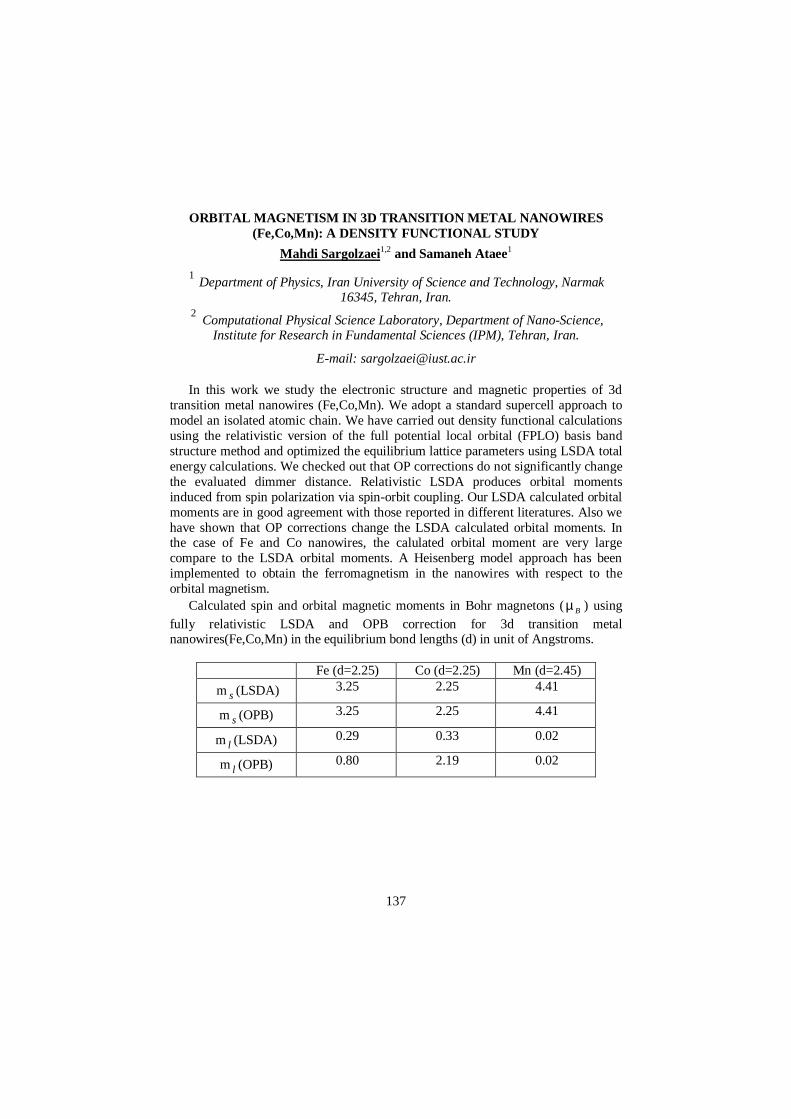
137
ORBITAL MAGNETISM IN 3D TRANSITION METAL NANOWIRES (Fe,Co,Mn): A DENSITY FUNCTIONAL STUDY
Mahdi Sargolzaei1,2 and Samaneh Ataee1
1 Department of Physics, Iran University of Science and Technology, Narmak
16345, Tehran, Iran. 2
Computational Physical Science Laboratory, Department of Nano-Science, Institute for Research in Fundamental Sciences (IPM), Tehran, Iran.
E-mail: [email protected]
In this work we study the electronic structure and magnetic properties of 3d transition metal nanowires (Fe,Co,Mn). We adopt a standard supercell approach to model an isolated atomic chain. We have carried out density functional calculations using the relativistic version of the full potential local orbital (FPLO) basis band structure method and optimized the equilibrium lattice parameters using LSDA total energy calculations. We checked out that OP corrections do not significantly change the evaluated dimmer distance. Relativistic LSDA produces orbital moments induced from spin polarization via spin-orbit coupling. Our LSDA calculated orbital moments are in good agreement with those reported in different literatures. Also we have shown that OP corrections change the LSDA calculated orbital moments. In the case of Fe and Co nanowires, the calulated orbital moment are very large compare to the LSDA orbital moments. A Heisenberg model approach has been implemented to obtain the ferromagnetism in the nanowires with respect to the orbital magnetism.
Calculated spin and orbital magnetic moments in Bohr magnetons ( Bµ ) using fully relativistic LSDA and OPB correction for 3d transition metal nanowires(Fe,Co,Mn) in the equilibrium bond lengths (d) in unit of Angstroms.
Fe (d=2.25) Co (d=2.25) Mn (d=2.45)
ms (LSDA) 3.25 2.25 4.41
m s (OPB) 3.25 2.25 4.41
m l (LSDA) 0.29 0.33 0.02
m l (OPB) 0.80 2.19 0.02
138
TWO ELECTRONIC STATES IN LAYERED QUANTUM DOTS
N.G. Aghekyan, E.M. Kazaryan, and H.A. Sarkisyan
Russian-Armenian University, 123 Hovsep Emin St., Yerevan 0051, Armenia
The properties of two-electronic states in layered quantum dots are considered. The Coulomb interaction between electrons is approximated by spherical generalization of Coulomb potential. The dependence of energy spectrum on geometrical parameters of layer is discussed.
139
AMPLITUDE SPECTROSCOPY OF TWO COUPLED JOSEPHSON QUBITS
M.V. Denisenko1, A.M. Satanin1, S. Ashhab2, and F. Nori2
1Nizhny Novgorod State University, Gagarin Ave., 23, 603950, Russia 2Advanced Science Institute, The Institute of Physical and Chemical Research
(RIKEN), Wako-shi, Saitama, 351-0198, Japan
E-mail, [email protected]
Recently a serious attention has been focused on the spectroscopy of Josephson junctions – superconducting circuits with a weak coupling which can be considered as “macroscopic atoms” with the sizes of the order of ten or hundreds micrometers [1]. The goal of this work is to describe quantum-mechanic phenomena in the system of coupled qubits from the point of view of quasi-energy states and investigate Landau-Zener transitions at different parameters of multi-level systems. The effect of a time-dependent driving field with a large amplitude on the system consisting of two coupled qubits (two-level systems) has been studied. Using the rotating wave approximation (RWA) made it possible to find simple conditions of a multi-level system resonant excitation. As it turned out the obtained conditions include the coupling constant of qubits. The numerical simulation carried out confirms qualitative conclusions following from RWA. When the field amplitude is large the system evolves adiabatically except for the immediate vicinity from quasi-crossing levels where Landau-Zener quantum-coherent transitions are observed. To reveal the peculiarities of resonant transitions caused by the quasi-level motion and crossing in a periodical driving field the Floquet states which determines the precise intermediate states of the system is applied [2]. The developed numerical method of calculating quasi-energy states of multi-level systems made it possible to find transition probabilities and build interference patterns for transition probabilities. The interference patterns demonstrate the possibility of obtaining some additional information about qubits since the positions of transition probability maxima appeared to be dependent on the coupling parameter of qubits.
The theory developed in this work allows to extend the amplitude spectroscopy method earlier effectively used for a single qubit over more complicated systems. It is evident that the quantum spectroscopy can be used for studying the spectra of artificial quantum objects: quantum wells, quantum dot, quantum wire and etc. in which the distances between energy levels are significantly smaller than in atomic ones.
References
[1] D. Berns, M.S.Runder, S.O.Valenzuela, K.K.Bergreen, W.D. Oliver, L.S.Levitov, T.P.Orlando, Amplitude spectroscopy of a solid-state artificial atom, Nature, 455, 51-57 (2008). [2] J.H. Shirley, Solution of the Schrodinger equation with a Hamiltonian periodic in time, Phys. Rev. 138, B979 B979-B987 (1965).
140
EXPERIMENTAL AND THEORETICAL INVESTIGATION ON HIGH- TC SUPERCONDUCTING INTRINSIC JOSEPHSON JUNCTIONS
Alexander Grib1,2, Yury Shukrinov3, Frank Schmidl1, and Paul Seidel1 1Institut für Festkörperphysik, Friedrich-Schiller-Universität Jena, D-07743 Jena,
Germany 2Physics Department, V. N. Karazin Kharkiv National University, 61077 Kharkiv, Ukraine
3Joint Institute for Nuclear Research, BLTP, Dubna, 141980, Russia
Within the last years many groups have realized and investigated different types of intrinsic Josephson junction (IJJ) arrays out of high-temperature superconducting single crystals or thin films. A short overview on the international status and results will be given.
We tried to improve the synchronization between the junctions by external shunts [1]. Mesa structures as well as microbridges on vicinal cut substrates showed multi-branch behaviour in their IV characteristics and random switching between branches [2]. Theoretical modelling was done investigating phase dynamics and stability numerically as well as analytically. Branch structure in current voltage characteristics of IJJ is studied in the framework of different models, particularly, in capacitevely coupled Josephson junctions (CCJJ) model and CCJJ model with diffusion current. We demonstrated that the inclusion of diffusion current might restore the equidistance of the branch structure [3]. The influence of microwave irradiation power on IV characteristics of IJJ is investigated [4]. We explained the experimental results by the competition between the “current effect” and the effect of suppression of the switching current by irradiation. Results of modelling of return current in IV characteristics for stacks with different number of IJJ are presented [5]. We discussed the possible mechanisms of synchronization and the ranges of stability [6]. Conclusions with respect to application of such arrays such as radiation sources were given [7].
This research was partially supported by Heisenberg-Landau Program and the German Research Foundation (DFG).
References [1] P.Seidel, A.N.Grib, Yu.M.Shukrinov, J.Scherbel, U.Huebner, F.Schmidl, Physica C, 362 (2001) 102-109. [2] A.N.Grib, M.Mans M, J.Scherbel, M.Buenfeld, F.Schmidl, P.Seidel, Supercond. Sci. Technol. 19 (2006), S 200- S 204. [3] Yu.M.Shukrinov, F.Mahfouzi, P.Seidel, Physica C 460–462 (2007) 1303–1304; Physica C, 449 (2006) 62-66. [4] Yu.M. Shukrinov, M.Mans, J Scherbel, P.Seidel, Supercond.Sci.Technol. 20 (2007) S74-S78 [5] Yu.M. Shukrinov, A. Irie, G.-I. Oya, M. Suzuki, N.F. Pedersen, and Paul Seidel, Ext. Abstr. ISEC, Fukuoka, Japan, June 16-19, 2009, TD-O2. [6] A.Grib, M.Mans, J.Scherbel, P.Seidel, Phys. Stat. Sol. B 242 (2005) 1286-1292. [7] A.Grib, P.Seidel, Phys. Stat. Sol. RRL 3 (2009) 302-304.
141
THE ORIGIN OF MULTIBRANCH IV-CHARACTERISTICS OF SHU NTED JOSEPHSON JUNCTION ARRAYS
Alexander Grib1,2 and Paul Seidel1 1Institut für Festkörperphysik, Friedrich-Schiller-Universität Jena, D-07743 Jena,
Germany 2Physics Department, V. N. Karazin Kharkiv National University, 61077 Kharkiv,
Ukraine
To model the IV-characteristics of shunted intrinsic Josephson junctions we calculated phase dynamics of a chain of two identical junctions covered by a resistive shunt and with a resistive crosspiece between the shunt and the junctions. The coherent solution of dynamic equations for this system is unstable at some bias currents above critical currents of junctions. We have shown that this instability leads to the multibranch structure of IV-curves in the hysteretic region. The multibranch structure appears due to the random switching of junctions to the superconducting state above their critical currents. We found that the resistance of the interface between a covering shunt and the junctions can regulate the multibranch behaviour.
142
FLUCTUATIONS OF PERSISTENT CURRENT
A.G. Semenov 1and A.D. Zaikin 1,2
1 I.E. Tamm Department of Theoretical Physics, P.N. Lebedev Physics Institute, 119991 Moscow, Russia
2 Institute for Nanotechnology, Karlsruhe Institute of Technology (KIT), 76021 Karlsruhe, Germany
E-mail: [email protected]
Meso- and nanorings formed by normal conductors and pierced by external magnetic flux develop persistent currents [1]. This fundamentally important equilibrium effect is a direct consequence of quantum coherence of electrons which -- at low enough temperatures -- may persist up to distances exceeding the perimeter of such rings.
Does persistent current (PC) fluctuate? At the first sight it might appear reasonable to assume that at least for 0→T no such fluctuations could occur. Indeed, while at non-zero T thermal fluctuations of PC should be present, in the zero temperature limit the system approaches its (non-degenerate) ground state and, hence, no PC fluctuations would be possible.
In our talk we will demonstrate that in many cases it is not so. Namely, no PC fluctuations are expected in the zero temperature limit only provided the current operator commutes with the total Hamiltonian of the system, otherwise fluctuations of persistent current can occur even in the ground state exactly at 0=T . Note that fluctuations of PC in the ground state may be induced provided the ring interacts with some quantum dissipative environment, but we consider entirely different situation: We do not assume the presence of interaction with any environment at all. Accordingly, quantum coherence of the system is fully preserved and no PC suppression takes place.
As a model we consider quantum particle of mass M on a 1d ring of radius R pierced by magnetic flux Φ . The particle position on the ring is parametrized by the angle θ which will be the quantum mechanical variable of interest in our problem. Also we add cosine potential with κ minima, so current operator does not commute with Hamiltonian [2]. We will present generating function, from which any current correlator can be easiy calculated. Second current cumulant is connected with power of PC fluctuations and we will discuss it in details in our talk.
References
[1] See, e.g., Y. Imry, Introduction to Mesoscopic Physics (Oxford University Press, Oxford, 1997). [2] A.G. Semenov and A.D. Zaikin, Phys. Rev. B 80, 155312 (2009).
143
QUANTUM WIRES AND TWO-DIMENSIONAL ELECTRON GASES WITH INHOMOGENEOUS RASHBA INTERACTION
Ll. Serra
Institut de Fsica Interdisciplinar i Sistemes Complexos IFISC (CSIC-UIB) Departament de Fsica, Universitat de les Illes Balears, E-07122 Palma de
Mallorca, Spain
E-mail: [email protected], http://ifisc.uib.es/
We discuss the physical properties of localized Rashba interactions in semiconductor quantum wires and two-dimensional electron gases. In quasi-one-dimensional semiconductor wires we show how the existence of quasibound states leads to Fano-Rashba resonances in the linear conductance. We investigate intersubband mixing effects in multichannel quantum wires attached to two magnetic contacts, the spin transistor geometry. When the contacts are ferromagnetic and their magnetization direction is perpendicular to the Rashba field, the spin-transistor current is expected to depend in an oscillatory way on the Rashba coupling strength due to spin coherent oscillations of the travelling electrons. Nevertheless, we find that the presence of many propagating modes strongly influences the spin precession effect, leading to (i) a quenching of the oscillations and (ii) strongly irregular curves for high values of the Rashba coupling. We also observe that in the case of leads' magnetization parallel to the Rashba field, the conductance departs from a uniform value as the Rashba strength increases. We also discuss the Rashba interaction induced current polarization effects when the contacts are not magnetic and investigate how this mechanism is affected by the presence of several propagating channels. The limit of the two-dimensional-electron-gas, when the transverse confinement vanishes and the system becomes translationally invariant in y direction is described. Our results [1] are discussed in the context of
recent measurements [2] and calculations [3,4].
References
[1] M.M. Gelabert, D. Sánchez, R. López, Ll. Serra, to be published. [2] H. C. Koo, J. H. Kwon, J. Eom, J. Chang, S. H. Han, M. Johnson, Science 325, 1515 (2009). [3] A. N. M. Zaiuddin, S. Hong, L. Siddiqui, S. Datta, ArXiv:1001.1523 (2010). [4] S. Bandyopadhyay, ArXiv:0911.0210 (2009).
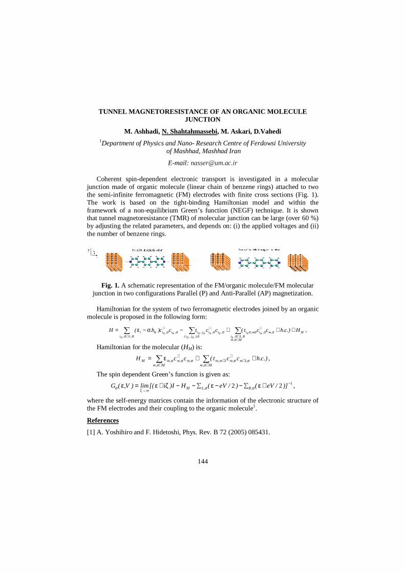
144
TUNNEL MAGNETORESISTANCE OF AN ORGANIC MOLECULE JUNCTION
M. Ashhadi, N. Shahtahmassebi, M. Askari, D.Vahedi
1Department of Physics and Nano- Research Centre of Ferdowsi University of Mashhad, Mashhad Iran
E-mail: [email protected]
Coherent spin-dependent electronic transport is investigated in a molecular junction made of organic molecule (linear chain of benzene rings) attached to two the semi-infinite ferromagnetic (FM) electrodes with finite cross sections (Fig. 1). The work is based on the tight-binding Hamiltonian model and within the framework of a non-equilibrium Green’s function (NEGF) technique. It is shown that tunnel magnetoresistance (TMR) of molecular junction can be large (over 60 %) by adjusting the related parameters, and depends on: (i) the applied voltages and (ii) the number of benzene rings.
Fig. 1. A schematic representation of the FM/organic molecule/FM molecular
junction in two configurations Parallel (P) and Anti-Parallel (AP) magnetization. Hamiltonian for the system of two ferromagnetic electrodes joined by an organic
molecule is proposed in the following form:
Hamiltonian for the molecular (HM) is:
,.)c.hcct(ccH ,mM,m
,mm,m,mM,m
,m,mM ++ε= σ+∈σ
+σ+σ
∈σ
+σσ ∑∑ 11
The spin dependent Green’s function is given as:
,)]/eV()/eV(HI)i[(lim)V,(G ,R,LM122 −
σσ∞→ζσ +ε∑−−ε∑−−ζ+ε=ε
where the self-energy matrices contain the information of the electronic structure of the FM electrodes and their coupling to the organic molecule1.
References
[1] A. Yoshihiro and F. Hidetoshi, Phys. Rev. B 72 (2005) 085431.
∑ ∑∑∈σ
∈σ∈σ
σ+
σσσσ
σ+
σσ+
σαα α
αααα
αααααα+++−σ−ε=
R,L,iM,m
R,L,iM,m,im,i
),j,i(,i,ij,i,i,ii ,H.)c.hcct(cctcc)h.(H
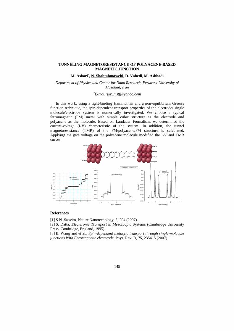
145
-2 -1 0 1 2
-4.0µ
-3.0µ
-2.0µ
-1.0µ
0.0
1.0µ
2.0µ
3.0µ
4.0µ
parallel antiparallel
Cur
ren
t(A
)
Voltage(V)-2 -1 0 1 2
-200.0n
0.0
200.0n
400.0n
600.0n
800.0n
1.0µ
1.2µ
1.4µ
1.6µ
parallel antiparallel
Cu
rre
nt(A
)
Gate Voltage(V)
TUNNELING MAGNETORESISTANCE OF POLYACENE-BASED MAGNETIC JUNCTION
M. Askari *, N. Shahtahmassebi, D. Vahedi, M. Ashhadi
Department of Physics and Center for Nano Research, Ferdowsi University of Mashhad, Iran
*E-mail:[email protected]
In this work, using a tight-binding Hamiltonian and a non-equilibrium Green's function technique, the spin-dependent transport properties of the electrode/ single molecule/electrode system is numerically investigated. We choose a typical ferromagnetic (FM) metal with simple cubic structure as the electrode and polyacene as the molecule. Based on Landauer Formalism, we determined the current-voltage (I-V) characteristic of the system. In addition, the tunnel magnetoresistance (TMR) of the FM/polyacene/FM structure is calculated. Applying the gate voltage on the polyacene molecule modified the I-V and TMR curves.
References
[1] S.N. Sanvito, Nature Nanotecnology, 2, 204 (2007). [2] S. Datta, Electeronic Transport in Mesoscopic Systems (Cambridge University Press, Cambridge, England, 1995). [3] B. Wang and et al., Spin-dependent inelasyic transport through single-molecule junctions With Feromagnetic electerode, Phys. Rev. B, 75, 235415 (2007).
-2 -1 0 1 2
0.30
0.35
0.40
0.45
0.50
0.55
0.60
0.65
TM
R
Bias Voltage(V)
Length of molecule:41
146
FIELD-EMISSION CURRENT FROM QUANTUM SYSTEM
G.V.Shpatakovskaya
IMM RAS, Moscow, Russia
E-mail: [email protected]
A universal semiclassical method is used and developed to calculate an emission current from a quantum system (atom, ion, metal cluster, metal surface, etc.) due to an outer electric field. It's assumed that the electron with the energy E is tunneling through a wide barrier. An expression for the tunneling probability and current are derived using the semiclassical 3D wave function. The field emission current is equal to
−ΨΣ∫∑ Σ
),(Im2
exp|)(||)(|)()(= 02
000000
exitEEEE
rrSrrpredEfm
eI
(1)
Here both a point r0 and the barrier exit point rexit belong to the same trajectory of the particle motion with the initial conditions r = r0, p = pE(r0); pE(r) = ∇SE(r) is the
momentum, ErE pdr
rS Γ∫0
=)( is the classical action, Γd is the arc element along the
trajectory, ppe /= is the unit momentum vector, ))((2=)( rUEmrpE −
(imaginary unit is related with the absolute value of the momentum vector), U(r) is a complete potential, Ψ0E is a free-field emitter electron wave function, which phase gradient is equal to the initial momentum vector pE(r0). The surface Σ0 is inside the barrier region. So Ψ0E(r) is required only in this area. The sum in the Eq.(1) is calculated over all the states of the emitter, f(E) = (1 + e(E − µ)/T)-1 is the Fermi distribution function, µ is a chemical potential.
The expression Eq. (1) is used to calculate the field-emission current from: 1. The spherical system (atom, negative ion, metal cluster). 2. The plane metal surface in the jellium model. The field-emission current
density J = I/σ is given by the same equation as in the paper [1], where the Bardeen transfer Hamiltonian method [2] has been used.
In the paper the image potential quantum calculation is discussed too.
This work was supported in part by Union State Programme SKIF-GRID (project 209Р420) and the Russian Foundation for Basic Research (project 08-01-00291)
References
[1] R. Ramprasad, L. R. C. Fonseca, and Paul von Allmen // Phys. Rev. B. 2000. 62. P. 5216. [2] Bardeen J. // Phys. Rev. Lett. 1961. 6.P. 57.
147
LONGITUDINAL PLASMA WAVE NUCLEATION IN COUPLED SYSTE M OF JOSEPHSON JUNCTIONS
Yu.M. Shukrinov 1 , M.Hamdipour 1,2
1 BLTP, JINR, Dubna, Moscow Region, 141980, Russia 2 Institute for Advanced Studies in Basic Sciences, P.O.Box 45195-1159, Zanjan,
Iran
E-mail: [email protected]
The investigation of the charge dynamics allows us to predict new physical properties of the coupled system of Josephson junctions [1]. The system is described by capacitively coupled Josephson junctions model with the diffusion current [2,3]. In [1,4] a correlation between the charge dynamics on the S-layers and features of IV-characteristics (CVC) was established and we showed that the breakpoint on the outermost branch of CVC is related to the parametric resonance in this system. Experimental manifestation of the breakpoint and the breakpoint region [5] in CVC of Bi2Sr2CaCu2Oy stimulates new investigations in this field.
In this paper we study the nucleation of LPW in the coupled system of JJ and find the different stages in the process of development of the LPW. We explain the shape of the charge signal in time and present the data concerning the charge distribution along the stack and the results of fast Fourier transformation analysis at different values of bias current. The answer to the fundamental question concerning the correspondence between the breakpoint's position in CVC and the parametric resonance region in time dependence of the charge on the S-layers is found: the position of the breakpoint on the outermost branch of CVC is related to the region with sharp increase of the amplitude of charge oscillation in the superconducting layers. We demonstrate that the onset of the increase of the oscillation amplitude can be shifted by noise in the bias current and microwave radiation. These effects open a way to regulate the process of LPW nucleation in the stack of JJ.
This research was supported by the Russian Foundation for Basic Research, grant 08-02-00520-a.
References
[1] Yu. M. Shukrinov, F. Mahfouzi, M. Suzuki, Phys.Rev.B, 78, 134521 (2008) [2] M. Machida, T. Koyama, A. Tanaka and M. Tachiki, Physica C330, 85 (2000) [3] Yu. M. Shukrinov, F. Mahfouzi, P. Seidel. Physica C449, 62 (2006). [4] Yu. M. Shukrinov, M. Hamdipour, M. R. Kolahchi. Phys. Rev. B, 80, 014512 (2009) [5] A. Irie, Yu. M. Shukrinov, G. Oya, Appl.Phys.Lett. 93, 152510, (2008).
148
QUANTUM SCATTERING ON VORTICES IN NANOPHYSICS
Yu.A. Sitenko
Bogolyubov Institute for Theoretical Physics, National Academy of Sciences, 03680, Kyiv, Ukraine
E-mail: [email protected]
Conical space emerges inevitably as an outer space of any topological defect of the vortex type. Quantum-mechanical scattering of a nonrelativistic particle by a vortex centred in conical space is considered, and effects of the transverse size of the vortex are taken into account. In nanophysics, one deals with topological defects (disclinations) in graphene -- strictly two-dimensional layer of carbon atoms. A disclination warps a sheet of graphene, rolling it into a nanocone with the deficit angle which can take both positive and negative values that are equal to multiples of
60 . We discuss some peculiarities of the high-frequency scattering which are due to the nonvanishing deficit angle.
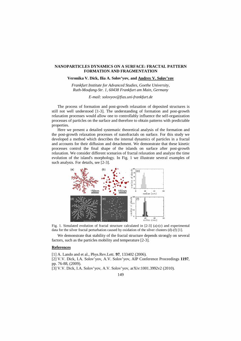
149
NANOPARTICLES DYNAMICS ON A SURFACE: FRACTAL PATTER N FORMATION AND FRAGMENTATION
Veronika V. Dick, Ilia A. Solov’yov, and Andrey V. Solov’yov
Frankfurt Institute for Advanced Studies, Goethe University, Ruth-Moufang-Str. 1, 60438 Frankfurt am Main, Germany
E-mail: [email protected]
The process of formation and post-growth relaxation of deposited structures is still not well understood [1-3]. The understanding of formation and post-growth relaxation processes would allow one to controllably influence the self-organization processes of particles on the surface and therefore to obtain patterns with predictable properties.
Here we present a detailed systematic theoretical analysis of the formation and the post-growth relaxation processes of nanofractals on surface. For this study we developed a method which describes the internal dynamics of particles in a fractal and accounts for their diffusion and detachment. We demonstrate that these kinetic processes control the final shape of the islands on surface after post-growth relaxation. We consider different scenarios of fractal relaxation and analyze the time evolution of the island's morphology. In Fig. 1 we illustrate several examples of such analysis. For details, see [2-3].
Fig. 1. Simulated evolution of fractal structure calculated in [2-3] (a)-(c) and experimental data for the silver fractal perturbation caused by oxidation of the silver clusters (d)-(f) [1].
We demonstrate that stability of the fractal structure depends strongly on several factors, such as the particles mobility and temperature [2-3].
References
[1] A. Lando and et al., Phys.Rev.Lett. 97, 133402 (2006). [2] V.V. Dick, I.A. Solov’yov, A.V. Solov’yov, AIP Conference Proceedings 1197, pp. 76-88, (2009). [3] V.V. Dick, I.A. Solov’yov, A.V. Solov’yov, arXiv:1001.3992v2 (2010).
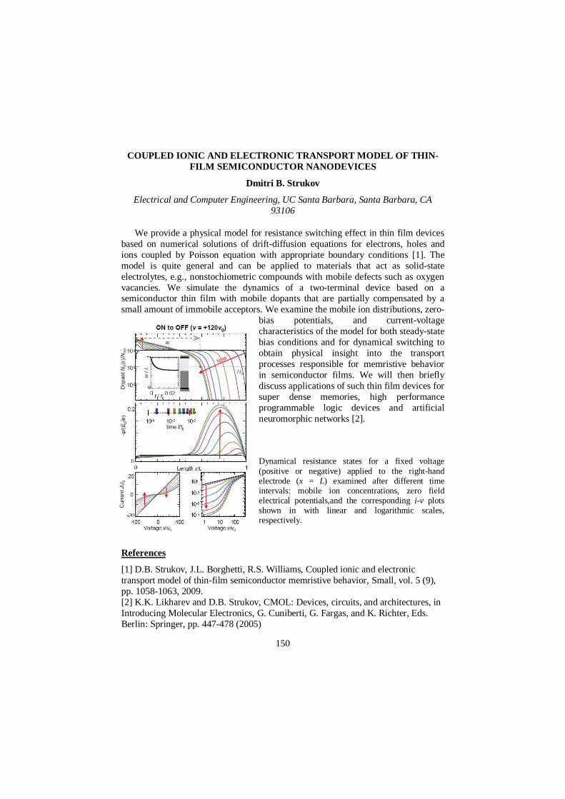
150
COUPLED IONIC AND ELECTRONIC TRANSPORT MODEL OF THI N-FILM SEMICONDUCTOR NANODEVICES
Dmitri B. Strukov
Electrical and Computer Engineering, UC Santa Barbara, Santa Barbara, CA 93106
We provide a physical model for resistance switching effect in thin film devices based on numerical solutions of drift-diffusion equations for electrons, holes and ions coupled by Poisson equation with appropriate boundary conditions [1]. The model is quite general and can be applied to materials that act as solid-state electrolytes, e.g., nonstochiometric compounds with mobile defects such as oxygen vacancies. We simulate the dynamics of a two-terminal device based on a semiconductor thin film with mobile dopants that are partially compensated by a small amount of immobile acceptors. We examine the mobile ion distributions, zero-
bias potentials, and current-voltage characteristics of the model for both steady-state bias conditions and for dynamical switching to obtain physical insight into the transport processes responsible for memristive behavior in semiconductor films. We will then briefly discuss applications of such thin film devices for super dense memories, high performance programmable logic devices and artificial neuromorphic networks [2].
Dynamical resistance states for a fixed voltage (positive or negative) applied to the right-hand electrode (x = L) examined after different time intervals: mobile ion concentrations, zero field electrical potentials,and the corresponding i-v plots shown in with linear and logarithmic scales, respectively.
References
[1] D.B. Strukov, J.L. Borghetti, R.S. Williams, Coupled ionic and electronic transport model of thin-film semiconductor memristive behavior, Small, vol. 5 (9), pp. 1058-1063, 2009. [2] K.K. Likharev and D.B. Strukov, CMOL: Devices, circuits, and architectures, in Introducing Molecular Electronics, G. Cuniberti, G. Fargas, and K. Richter, Eds. Berlin: Springer, pp. 447-478 (2005)
151
THE SELF INTERACTION CORRECTION REVISITED
J. Messud1 , P. M. Dinh1 , E. Suraud1 , P. G. Reinhard2
1Laboratoire de Physique Thйorique, UMR 5152, Universitй Paul Sabatier, 118 route de Narbonne, F-31062 Toulouse Cedex, France
2 Institut fьr Theoretische Physik, Universitдt Erlangen Staudtstr. 7, D-91058 Erlangen, Germany
The Self Interaction Correction (SIC) is a long standing problem in Density Functional Theory (DFT). It causes several major difficulties especially with the universally used simple and efficient Local Density Approximation (LDA). The standard SIC approaches lead to the introduction of orbital dependent functional which exhibit several formal and technical problems. The Optimized Effectove Potential (OEP) methods allow to deal with such difficulties but in an approximate manner. The fully time dependent cases remain especially problematic, which leads to significant difficulties for the treatment of ionization "on the fly".
We discuss an extension of time-dependent DFT including SIC. A strictly variational formulation is given taking care of the necessary constraints. A manageable and transparent propagation scheme using two sets of wavefunctions is proposed and applied to laser excitation with subsequent ionization of a dimer molecule.
We also propose a simplification of the Optimized Effective Potential (OEP) applied to the Self Interaction Correction (SIC) scheme of Density Functional Theory (DFT). The new scheme acceptably fulfills several key formal properties and turns out to be both simple and accurate. We show examples of applications on model molecules in terms of observables known to be especially sensitive to details of the SIC-OEP approach. This latter approach might be applicable to low energy phenomena.
152
KINETICS OF CLUSTER GROWTH IN FULLERENE C 60 SOLUTIONS IN NITROGEN-CONTAINING SOLVENTS
V.L. Aksenov, T.V. Tropin, M.V. Avdeev
Frank Laboratory of Neutron Physics, Joint Institute for Nuclear Research, 141980 Dubna, Russia
Russian Research Centre Kurchatov Institute, pl. Akademika Kurchatova 1, 123182 Moscow, Russia
Cluster growth processes occurring in fullerene C60 solutions draw much attention of researchers because of promising practical applications. The clusters solution of C60 in nitrogen-containing solvents (e.g. N-methyl-2-pyrrolidone (NMP), pyridine) can be regarded as a “model” system for verification of various theoretical approaches to describing the kinetics of cluster growth. Also, the successful solution of this problem may lead to certain new ideas concerning description of fullerene-water colloidal solutions. The observed slow growth of large clusters (~500 nm sizes are reached within several weeks) of C60 macromolecules in NMP and pyridine offers a good opportunity to apply the approach of kinetic theory of nucleation.
In the present work several models for description of cluster growth in C60/NMP and C60/Py solution are considered. In addition to basic approach nucleation theory these models take account of the confinement of cluster growth due to possible formation of donor-acceptor complexes between C60 and solvent molecules. A modification of basic kinetic equations results in additional model parameter– characteristic time of C60-solvent complex formation, τ. Some different ways to introduce confinement are proposed. The most appropriate model is selected on the basis of agreement with experimental results and simplicity. Estimation of models parameters is made with the use of experimental data. The final sizes of the clusters in C60/NMP and C60/Py have been measured lately by small-angle neutron scattering (SANS), dynamic light scattering (DLS) and electron microscopy (EM) techniques. Additionally, the experimental data of extraction of C60 monomers from C60/NMP solution to hexane, prove to be very valuable for control of theoretically obtained results on time-scale.
As a result, a model of confined growth of clusters in C60 solutions in nitrogen-containing solvents is proposed, its parameters estimated and the results compared with experiment. The consequences of the model are discussed, including the obtained evolution of cluster distribution with time.
153
PROXIMITY INDUCED SPIN ORDERING AT THE FERROMAGNETI C METAL/DILUTE MAGNETIC SEMICONDUCTOR INTERFACE
V.V. Tugushev
Departamento de Fisica de Materiales, Facultad de Ciencias Quimicas, UPV/EHU, 20080,
P. Manuel Lardizabal,3, Donostia-San Sebastian, Basque Country, Spain
We investigate theoretically the conditions for the appearance and/or modification of spin ordering in a dilute magnetic semiconductor contacted to a ferromagnetic metal. We show that the magnetic proximity effect has complicated enough physical nature in this system. Allowing for both the electron scattering and hybridization between the ferromagnetic metal and semiconductor electron states at the interface, we calculate the spin polarization of carriers in a semiconductor layer near the interface. The peculiar mechanism of indirect exchange coupling between local spins dissolved in the semiconductor host, which occurs when a dilute magnetic semiconductor is contacted to a ferromagnetic metal,is analyzed. The structure of the proximity induced spin ordering in a dilute magnetic semiconductor is qualitatively described in frame of a mean field approach. The interpretation of experimental data on the Fe/(Ga,Mn)As and Py/(Ga,Mn)As layered structures is done.
154
PHASE DIAGRAM OF THE BILAYER SYSTEM AT 1=ν
A.V. Bunyakin, A.A. Vasilchenko
Kuban State Technological University, Krasnodar, Moskovskay 2, Russia
E-mail: [email protected]
We have investigated the electronic structure of vertically coupled double quantum dots in magnetic field within local density functional theory. The dots are identical and two-dimensional. Many-body effects are taken approximately into account by the use of local intra-layer exchange energy.
The system of Kohn-Sham equations for vertically coupled quantum dots in a magnetic field with the number of electrons up to 100 was solved numerically. We studied the transition from the maximum-density-droplet state of isospin-polarized electrons (the quantum Hall state) in the state with number of electrons occupying antisymmetric state Na = 1. Phase diagram for the bilayer system in the magnetic field – tunneling splitting plane was constructed. It is shown that at low electron density quantum Hall state is energetically favorable in the structure with zero tunneling splitting.
This work is supported by RFBR and administration of Krasnodar region.
155
DENSITY OF ELECTRONIC STATES IN GRAPHENE WITH IMPURI TIES
N.D. Vlasii
Bogolyubov Institute for Theoretical Physics, National Academy of Sciences, 03680, Kyiv, Ukraine
E-mail: [email protected]
A synthesis of strictly twodimensional atomic crystals (monolayers of carbon atoms) is promising a wealth of new phenomena and possible applications in technology and industry. Such materials are characterized by the Dirac-type spectrum of quasiparticle excitations, yielding a unique example of the truly twodimensional "relativistic" electronic system which possesses rather unusual properties. We accomplish a comprehensive study of the role of impurities of the point vortex type. Both global and local densities of states are evaluated. We consider both flat and curved nanolayers and point out observable effects of the layer geometry.
156
DETONATION NANODIAMONDS AS A NEW CARBON NANOSTRUCTURE FOR NANOTECHNOLOGY
A.Ya. Vul’
Ioffe Physical-Technical Institute of the Russian Academy of Sciences
E-mail: [email protected]
Development of nanotechnology requires the production of dispersed particles of a material with characteristic sizes of a few nanometers. Detonation nanodiamond (DND) has a crystalline core of about 4 nm. The goal of presentation is to give a short review on technology, properties and applications of DND produced by detonation of carbon explosive materials discovered in USSR in the 60-s. The presentation based on the latest results of Ioffe Institute nanodiamond group [1,2].
It has been recently shown by Ioffe Institute group as well as other scientists the DND cluster consists of a diamond core (sp3 hybridized carbon) covered by a carbon-onion shell (sp2 hybridized carbon). It has been experimentally shown that the sp3/sp2 depends strongly on conditions of detonation synthesis and can be changed by heat treatment in different atmosphere.
It has been difficult to isolate the crystalline cores primarily because of the well-known high tendency for nano-sized particles to aggregate into clusters of submicron size due to the high specific surface area. DND usually forms a hierarchical fractal structure. However, it was recently suggested that stirred-media milling with micron-sized zirconia beads is an effective method for making from DND stable aqueous suspension of 4 nm particles.
Besides well-known applications of DND for polishing material, metal-nanodiamond coatings, and polymer composites and rubbers new applications are discussed in the last time. Among them we would like to emphasized composites with high thermal conductivity, field electron emission, seeding at growing of CVD diamond films, production of new magnetic materials and materials for bio-medical applications. In this connections the most important step is development of industrial scaled technology for production of the stable nanodiamond particle suspension and the technology of surface functionalization of the single 4 nm diamond particle. The applications mentioned above are discussed in presentation.
The research has been supporting by the FASI, the Russian Academy of Sciences, RFBR and European FP7 program.
References:
[1] Baidakova M., Vul’ A. Journal Phys. D: Appl. Phys. 40, 6300-311 (2007). [2] Vul’ A.Ya., Aleksenskiy A.. E., Dideykin A. T. In: Nanosciences and Nanotechnologies, Eds. V. Kharkin, Chunli Bai, Sae-Chul Kim. Encyclopedia of Life Support Systems (EOLSS) UNESCO, EOLSS Publishers, Oxford ,UK (http://www.eolss.net) (2009).
157
TERAHERTZ EMISSION FROM INTRINSIC JOSEPHSON JUNCTIONS AT HIGH BIAS AND LOW BIAS
H. B. Wang1, S. Guenon2, J. Yuan1, Z. G. Jiang3, Y. Y. Zhong3, P. H. Wu3, A. Iishi1, T. Hatano1, B. Gross2, M. Gruenzweig2, D. Koelle2, and R. Kleiner2
1 National Institute for Materials Science, Tsukuba 3050047, Japan 2 Physikalisches Institut Experimentalphysik II and Center for Collective Quantum
Phenomena, Universitaet Tuebingen, Auf der Morgenstelle 14, D-72076 Tuebingen, Germany
3 Research Institute of Superconductor Electronics, Nanjing University, Nanjing 210093, China
To have practical applications with THz emission from intrinsic Josephson junctions, the following conditions should be satisfied: tunable operation frequencies, narrow linewidth, high power output and good stability. In low bias and high bias regimes [1,2], THz emission from intrinsic Josephson junctions has been observed by bolometric detection. In the talk, I will show the remarkable difference of THz emission between these two regimes, and discuss the role of a hotspot appearing in the high bias regime. I will convince you with our results that the THz emission at high bias may have feasible applications..
References
[1] L. Ozyuzer, A. E. Koshelev, C. Kurter, N. Gopalsami, Q. Li, M. Tachiki, K. Kadowaki, T. Yamamoto, H. Minami, H. Yamaguchi, et al., Science 318, 1291 (2007). [2] H. B. Wang, S. Guénon, J. Yuan, A. Iishi, S. Arisawa, T. Hatano, T. Yamashita, D. Koelle, and R. Kleiner, Phys. Rev. Lett. 102, 017006 (2009).
158
THE EFFECT OF SURFACTANTS ON CHEMICAL DEVELOPMENTS OF ION TRACKS IN POLYMERS
Yu. Yamauchi, P. Yu. Apel
FLNR, JINR, Dubna, Moscow Region, 141980, Russia
The surfactant molecules form a quasi-solid adsorption layer on polyethylene terephthalate (PET) films and protects partially the surface, which leads to a reduction in the bulk etch rate of the solids [1]. In general, the protection effect depends on the alkali concentration, temperature and type of surfactant [2]. The pore geometry critically depends on the peculiarities of the diffusion of surfactant into restricted volumes. It was shown in Ref.[1] that the addition of sodium dodecyl diphenyloxide disulphonate (SDDD) to the alkali solution leads to the formation of the highly tapered pore profile. In this paper we study the diffusion and adsorption of SDDD on non-etched non-porous, etched non-porous and etched porous PET films. The comparison of non-etched non-porous and etched non-porous films shows the effect of negatively charged surface on the adsorption of surfactant. The comparison of etched non-porous and etched porous PET films shows the different adsorption on film surface and inner wall of pore, thus the influence of curvature of the surface on the adsorption of surfactant molecules. We discuss the application of our results for the efficient control of the structural characteristics of track membranes.
References
[1] P. Yu. Apel, I. V. Blonskaya, A. Yu. Didyk, S. D. Dmitriev, O. L. Orelovitch, D. Root, L.I. Samoilova, V. A. Vutsadakis, Nucl. Instr. and Meth., Phys. Res. B 179, 55 (2001). [2] P. Yu. Apel, I. V. Blonskaya, S. D. Dmitriev, T. I. Mamonova, O. L. Orelovitch, B. Sartowska, Yu. Yamauchi, Radiation Measurements, 43, S552 (2008).
159
QUANTUM DOT SUPERRADIANT EMISSION
V.I. Yukalov 1 and E.P. Yukalova2 1 Laboratory of Theoretical Physics, Joint Institute for Nuclear Research,
141980 Dubna, Russia 2 Laboratory of Information Technologies, Joint Institute for Nuclear Research,
141980 Dubna, Russia
E-mail: [email protected]
The possibility of realizing the superradiant regime of electromagnetic emission by the assembly of quantum dots is considered. The overall dynamical process is analyzed in detail. It is shown that there can occur several qualitatively different stages of evolution. The process starts with dipolar waves triggering the spontaneous radiation of individual dots. This corresponds to the fluctuation stage, when the dots are not yet noticeably correlated with each other. The second is the quantum stage, when the dot interactions through the common radiation field become more important, but the coherence is not yet developed. The third is the coherent stage, when the dots radiate coherently, emitting a superradiant pulse. After the superradiant pulse, the system of dots relaxes to an incoherent state in the relaxation stage. If there is no external permanent pumping, or the effective dot interactions are weak, the system tends to a stationary state during the last stationary stage, when coherence dies out to a low, practically negligible, level. In the case of permanent pumping, there exists the sixth stage of pulsing superradiance, when the system of dots emits separate coherent pulses.
References
[1] V.I. Yukalov and E.P. Yukalova, Dynamics of quantum-dot superradiance. Phys. Rev. B (2010) accepted.
160
SHOT NOISE AND COULOMB BLOCKADE OF ANDREEV REFLECTI ON
A.D. Zaikin
Institute for Nanotechnology, Karlsruhe Institute of Technology (KIT), 76021 Karlsruhe, Germany
I.E. Tamm Department of Theoretical Physics, P.N. Lebedev Physics Institute, 119991 Moscow, Russia
E-mail: [email protected]
We derive low energy effective action for a short coherent conductor between normal (N) and superconducting (S) reservoirs [1]. We evaluate interaction correction Gδ to Andreev conductance and highlight a fundamental relation between interaction effects and shot noise in NS systems. In the diffusive limit doubling of both shot noise power and charge of the carriers yields || Gδ four times bigger than in the normal case. We further generalize our effective action formalism to describe interaction effects on non-local electron transport in three-terminal NSN structures [2]. We demonstrate that the non-linear non-local conductance of such devices can acquire a non-trivial S -shape which is a unique signature of electron-electron interactions. Our predictions [1,2] can quantitatively explain recent experimental observations [3,4] and can further be tested in future experiments.
References
[1] A.V. Galaktionov and A.D. Zaikin, Shot noise and Coulomb blocade of Andreev reflection. Phys. Rev. B, 80, 174527 (2009). [2] D.S. Golubev and A.D. Zaikin, Coulomb blockade of non-local electron transport. Preprint (2010). [3] A. T. Bollinger, A. Rogachev, and A. Bezryadin, Dichotomy in short superconducting nanowires: thermal phase slippage vs. Coulomb blockade. Europhys. Lett. 76, 505 (2006). [4] J. Brauer, F. Hьbler, M. Smetanin, D. Beckmann, and H. v. Lцhneysen, Non-local transport in normal-metal/superconductor hybrid structures: the role of interference and interaction. ArXiv:0912.0123 (2009).
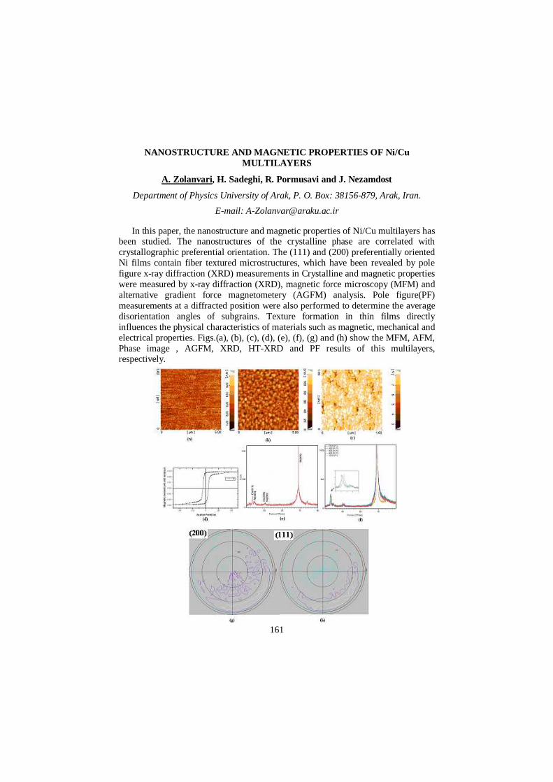
161
NANOSTRUCTURE AND MAGNETIC PROPERTIES OF Ni/Cu MULTILAYERS
A. Zolanvari, H. Sadeghi, R. Pormusavi and J. Nezamdost
Department of Physics University of Arak, P. O. Box: 38156-879, Arak, Iran.
E-mail: [email protected]
In this paper, the nanostructure and magnetic properties of Ni/Cu multilayers has been studied. The nanostructures of the crystalline phase are correlated with crystallographic preferential orientation. The (111) and (200) preferentially oriented Ni films contain fiber textured microstructures, which have been revealed by pole figure x-ray diffraction (XRD) measurements in Crystalline and magnetic properties were measured by x-ray diffraction (XRD), magnetic force microscopy (MFM) and alternative gradient force magnetometery (AGFM) analysis. Pole figure(PF) measurements at a diffracted position were also performed to determine the average disorientation angles of subgrains. Texture formation in thin films directly influences the physical characteristics of materials such as magnetic, mechanical and electrical properties. Figs.(a), (b), (c), (d), (e), (f), (g) and (h) show the MFM, AFM, Phase image , AGFM, XRD, HT-XRD and PF results of this multilayers, respectively.