Embed Size (px)
Citation preview
74AVC1T45Dual-supply voltage level translator/transceiver; 3-stateRev. 8 — 10 December 2018 Product data sheet
1. General descriptionThe 74AVC1T45 is a single bit, dual supply transceiver with 3-state output that enablesbidirectional level translation. It features two 1-bit input-output ports (A and B), a direction controlinput (DIR) and dual supply pins (VCC(A) and VCC(B)). Both VCC(A) and VCC(B) can be supplied at anyvoltage between 0.8 V and 3.6 V making the device suitable for translating between any of the lowvoltage nodes (0.8 V, 1.2 V, 1.5 V, 1.8 V, 2.5 V and 3.3 V). Pins A and DIR are referenced to VCC(A)and pin B is referenced to VCC(B). A HIGH on DIR allows transmission from A to B and a LOW onDIR allows transmission from B to A.
The device is fully specified for partial power-down applications using IOFF. The IOFF circuitrydisables the output, preventing any damaging backflow current through the device when it ispowered down. In suspend mode when either VCC(A) or VCC(B) are at GND level, both A and B arein the high-impedance OFF-state.
2. Features and benefits• Wide supply voltage range:
• VCC(A): 0.8 V to 3.6 V• VCC(B): 0.8 V to 3.6 V
• High noise immunity• Complies with JEDEC standards:
• JESD8-12 (0.8 V to 1.3 V)• JESD8-11 (0.9 V to 1.65 V)• JESD8-7 (1.2 V to 1.95 V)• JESD8-5 (1.8 V to 2.7 V)• JESD8-B (2.7 V to 3.6 V)
• ESD protection:• HBM JESD22-A114E Class 3B exceeds 8000 V• MM JESD22-A115-A exceeds 200 V• CDM JESD22-C101C exceeds 1000 V
• Maximum data rates:• 500 Mbit/s (1.8 V to 3.3 V translation)• 320 Mbit/s (< 1.8 V to 3.3 V translation)• 320 Mbit/s (translate to 2.5 V or 1.8 V)• 280 Mbit/s (translate to 1.5 V)• 240 Mbit/s (translate to 1.2 V)
• Suspend mode• Latch-up performance exceeds 100 mA per JESD 78 Class II• Inputs accept voltages up to 3.6 V• Low noise overshoot and undershoot < 10 % of VCC• IOFF circuitry provides partial Power-down mode operation• Multiple package options• Specified from -40 °C to +85 °C and -40 °C to +125 °C
Nexperia 74AVC1T45Dual-supply voltage level translator/transceiver; 3-state
3. Ordering information
Table 1. Ordering informationPackageType numberTemperature range Name Description Version
74AVC1T45GW -40 °C to +125 °C SC-88 plastic surface-mounted package; 6 leads SOT363
74AVC1T45GM -40 °C to +125 °C XSON6 plastic extremely thin small outline package; no leads;6 terminals; body 1 x 1.45 x 0.5 mm
SOT886
74AVC1T45GN -40 °C to +125 °C XSON6 extremely thin small outline package; no leads;6 terminals; body 0.9 x 1.0 x 0.35 mm
SOT1115
74AVC1T45GS -40 °C to +125 °C XSON6 extremely thin small outline package; no leads;6 terminals; body 1.0 x 1.0 x 0.35 mm
SOT1202
74AVC1T45GX -40 °C to +125 °C X2SON6 plastic thermal extremely thin small outline package;no leads; 6 terminals; body 1 x 0.8 x 0.35 mm
SOT1255
4. Marking
Table 2. MarkingType number Marking code[1]74AVC1T45GW B5
74AVC1T45GM B5
74AVC1T45GN B5
74AVC1T45GS B5
74AVC1T45GX B5
[1] The pin 1 indicator is located on the lower left corner of the device, below the marking code.
5. Functional diagram
001aag885
VCC(B)VCC(A)
5DIR
3A
B4
Fig. 1. Logic symbol
001aag886
VCC(B)VCC(A)
DIR
A
B
Fig. 2. Logic diagram
74AVC1T45 All information provided in this document is subject to legal disclaimers. © Nexperia B.V. 2018. All rights reserved
Product data sheet Rev. 8 — 10 December 2018 2 / 22

Nexperia 74AVC1T45Dual-supply voltage level translator/transceiver; 3-state
6. Pinning information
6.1. Pinning
74AVC1T45
VCC(A) VCC(B)
GND
A B
001aag971
1
2
3
6
DIR5
4
Fig. 3. Pin configuration SOT363
74AVC1T45
GND
001aag972
VCC(A)
A
DIR
VCC(B)
B
Transparent top view
2
3
1
5
4
6
Fig. 4. Pin configuration SOT886
aaa-000876
74AVC1T45
Transparent top view
1 6VCC(A) VCC(B)
2 5GND DIR
3 4A B
Fig. 5. Pin configuration SOT1115 and SOT1202
aaa-022602Transparent top view
74AVC1T45
3 4A B
1 6VCC(A) VCC(B)
2GND 5 DIR
Fig. 6. Pin configuration SOT1255 (X2SON6)
6.2. Pin description
Table 3. Pin descriptionSymbol Pin DescriptionVCC(A) 1 supply voltage port A and DIR
GND 2 ground (0 V)
A 3 data input or output
B 4 data input or output
DIR 5 direction control
VCC(B) 6 supply voltage port B
74AVC1T45 All information provided in this document is subject to legal disclaimers. © Nexperia B.V. 2018. All rights reserved
Product data sheet Rev. 8 — 10 December 2018 3 / 22
Nexperia 74AVC1T45Dual-supply voltage level translator/transceiver; 3-state
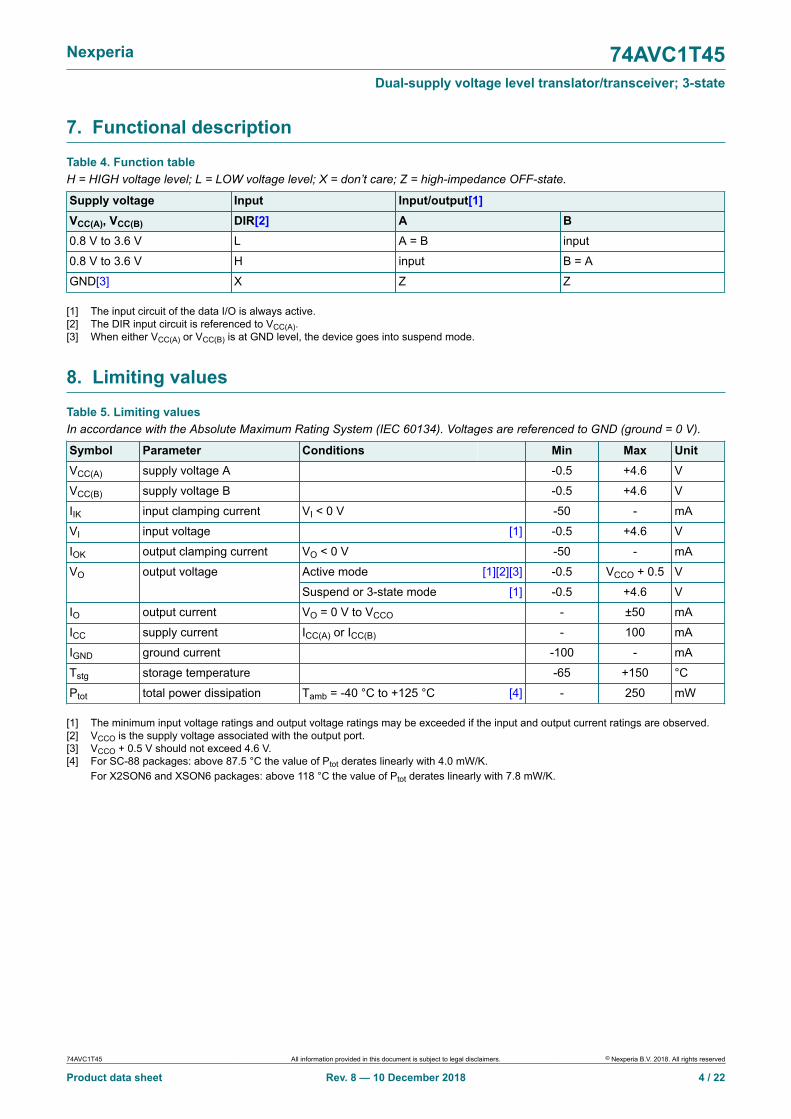
7. Functional description
Table 4. Function tableH = HIGH voltage level; L = LOW voltage level; X = don’t care; Z = high-impedance OFF-state.
Supply voltage Input Input/output[1]VCC(A), VCC(B) DIR[2] A B0.8 V to 3.6 V L A = B input
0.8 V to 3.6 V H input B = A
GND[3] X Z Z
[1] The input circuit of the data I/O is always active.[2] The DIR input circuit is referenced to VCC(A).[3] When either VCC(A) or VCC(B) is at GND level, the device goes into suspend mode.
8. Limiting values
Table 5. Limiting valuesIn accordance with the Absolute Maximum Rating System (IEC 60134). Voltages are referenced to GND (ground = 0 V).
Symbol Parameter Conditions Min Max UnitVCC(A) supply voltage A -0.5 +4.6 V
VCC(B) supply voltage B -0.5 +4.6 V
IIK input clamping current VI < 0 V -50 - mA
VI input voltage [1] -0.5 +4.6 V
IOK output clamping current VO < 0 V -50 - mA
Active mode [1][2][3] -0.5 VCCO + 0.5 VVO output voltage
Suspend or 3-state mode [1] -0.5 +4.6 V
IO output current VO = 0 V to VCCO - ±50 mA
ICC supply current ICC(A) or ICC(B) - 100 mA
IGND ground current -100 - mA
Tstg storage temperature -65 +150 °C
Ptot total power dissipation Tamb = -40 °C to +125 °C [4] - 250 mW
[1] The minimum input voltage ratings and output voltage ratings may be exceeded if the input and output current ratings are observed.[2] VCCO is the supply voltage associated with the output port.[3] VCCO + 0.5 V should not exceed 4.6 V.[4] For SC-88 packages: above 87.5 °C the value of Ptot derates linearly with 4.0 mW/K.
For X2SON6 and XSON6 packages: above 118 °C the value of Ptot derates linearly with 7.8 mW/K.
74AVC1T45 All information provided in this document is subject to legal disclaimers. © Nexperia B.V. 2018. All rights reserved
Product data sheet Rev. 8 — 10 December 2018 4 / 22
Nexperia 74AVC1T45Dual-supply voltage level translator/transceiver; 3-state
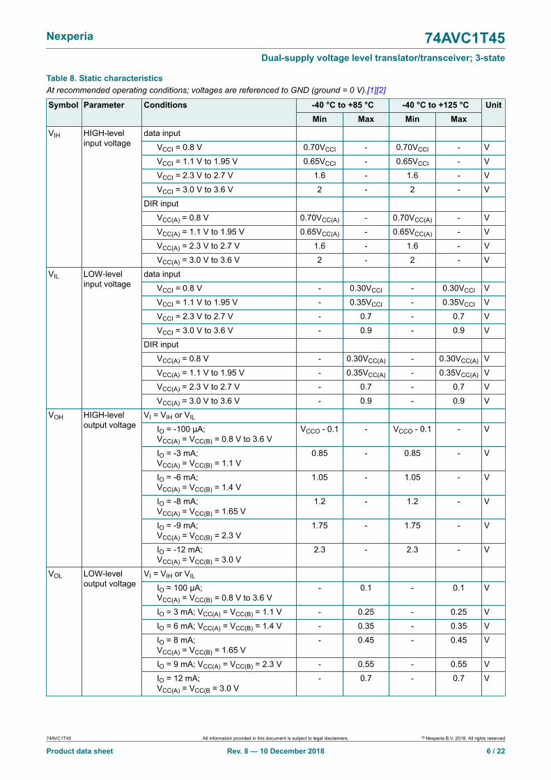
9. Recommended operating conditions
Table 6. Recommended operating conditionsSymbol Parameter Conditions Min Max UnitVCC(A) supply voltage A 0.8 3.6 V
VCC(B) supply voltage B 0.8 3.6 V
VI input voltage 0 3.6 V
Active mode [1] 0 VCCO VVO output voltage
Suspend or 3-state mode 0 3.6 V
Tamb ambient temperature -40 +125 °C
Δt/ΔV input transition rise and fall rate VCCI = 0.8 V to 3.6 V [2] - 5 ns/V
[1] VCCO is the supply voltage associated with the output port.[2] VCCI is the supply voltage associated with the input port.
10. Static characteristics
Table 7. Typical static characteristicsAt recommended operating conditions; voltages are referenced to GND (ground = 0 V).[1]
Tamb = 25 °CSymbol Parameter ConditionsMin Typ Max
Unit
VI = VIH or VILVOH HIGH-level output voltage
IO = -1.5 mA; VCC(A) = VCC(B) = 0.8 V - 0.69 - V
VI = VIH or VILVOL LOW-level output voltage
IO = 1.5 mA; VCC(A) = VCC(B) = 0.8 V - 0.07 - V
II input leakage current DIR input; VI = 0 V or 3.6 V;VCC(A) = VCC(B) = 0.8 V to 3.6 V
- ±0.025 ±0.25 μA
IOZ OFF-state output current A or B port; VO = 0 V or VCCO;VCC(A) = VCC(B) = 0.8 V to 3.6 V
[2] - ±0.5 ±2.5 μA
A port; VI or VO = 0 V to 3.6 V; VCC(A) = 0 V;VCC(B) = 0.8 V to 3.6 V
- ±0.1 ±1 μAIOFF power-off leakage current
B port; VI or VO = 0 V to 3.6 V; VCC(B) = 0 V;VCC(A) = 0.8 V to 3.6 V
- ±0.1 ±1 μA
CI input capacitance DIR input; VI = 0 V or 3.3 V;VCC(A) = VCC(B) = 3.3 V
- 1.0 - pF
CI/O input/output capacitance A and B port; Suspend mode;VO = VCCO or GND; VCC(A) = VCC(B) = 3.3 V
- 4.0 - pF
[1] VCCO is the supply voltage associated with the output port.[2] For I/O ports, the parameter IOZ includes the input leakage current.
74AVC1T45 All information provided in this document is subject to legal disclaimers. © Nexperia B.V. 2018. All rights reserved
Product data sheet Rev. 8 — 10 December 2018 5 / 22
Nexperia 74AVC1T45Dual-supply voltage level translator/transceiver; 3-state
Table 8. Static characteristicsAt recommended operating conditions; voltages are referenced to GND (ground = 0 V).[1][2]
-40 °C to +85 °C -40 °C to +125 °CSymbol Parameter ConditionsMin Max Min Max
Unit
data input
VCCI = 0.8 V 0.70VCCI - 0.70VCCI - V
VCCI = 1.1 V to 1.95 V 0.65VCCI - 0.65VCCI - V
VCCI = 2.3 V to 2.7 V 1.6 - 1.6 - V
VCCI = 3.0 V to 3.6 V 2 - 2 - V
DIR input
VCC(A) = 0.8 V 0.70VCC(A) - 0.70VCC(A) - V
VCC(A) = 1.1 V to 1.95 V 0.65VCC(A) - 0.65VCC(A) - V
VCC(A) = 2.3 V to 2.7 V 1.6 - 1.6 - V
VIH HIGH-levelinput voltage
VCC(A) = 3.0 V to 3.6 V 2 - 2 - V
data input
VCCI = 0.8 V - 0.30VCCI - 0.30VCCI V
VCCI = 1.1 V to 1.95 V - 0.35VCCI - 0.35VCCI V
VCCI = 2.3 V to 2.7 V - 0.7 - 0.7 V
VCCI = 3.0 V to 3.6 V - 0.9 - 0.9 V
DIR input
VCC(A) = 0.8 V - 0.30VCC(A) - 0.30VCC(A) V
VCC(A) = 1.1 V to 1.95 V - 0.35VCC(A) - 0.35VCC(A) V
VCC(A) = 2.3 V to 2.7 V - 0.7 - 0.7 V
VIL LOW-levelinput voltage
VCC(A) = 3.0 V to 3.6 V - 0.9 - 0.9 V
VI = VIH or VIL
IO = -100 μA;VCC(A) = VCC(B) = 0.8 V to 3.6 V
VCCO - 0.1 - VCCO - 0.1 - V
IO = -3 mA;VCC(A) = VCC(B) = 1.1 V
0.85 - 0.85 - V
IO = -6 mA;VCC(A) = VCC(B) = 1.4 V
1.05 - 1.05 - V
IO = -8 mA;VCC(A) = VCC(B) = 1.65 V
1.2 - 1.2 - V
IO = -9 mA;VCC(A) = VCC(B) = 2.3 V
1.75 - 1.75 - V
VOH HIGH-leveloutput voltage
IO = -12 mA;VCC(A) = VCC(B) = 3.0 V
2.3 - 2.3 - V
VI = VIH or VIL
IO = 100 μA;VCC(A) = VCC(B) = 0.8 V to 3.6 V
- 0.1 - 0.1 V
IO = 3 mA; VCC(A) = VCC(B) = 1.1 V - 0.25 - 0.25 V
IO = 6 mA; VCC(A) = VCC(B) = 1.4 V - 0.35 - 0.35 V
IO = 8 mA;VCC(A) = VCC(B) = 1.65 V
- 0.45 - 0.45 V
IO = 9 mA; VCC(A) = VCC(B) = 2.3 V - 0.55 - 0.55 V
VOL LOW-leveloutput voltage
IO = 12 mA;VCC(A) = VCC(B = 3.0 V
- 0.7 - 0.7 V
74AVC1T45 All information provided in this document is subject to legal disclaimers. © Nexperia B.V. 2018. All rights reserved
Product data sheet Rev. 8 — 10 December 2018 6 / 22
Nexperia 74AVC1T45Dual-supply voltage level translator/transceiver; 3-state
-40 °C to +85 °C -40 °C to +125 °CSymbol Parameter ConditionsMin Max Min Max
Unit
II input leakagecurrent
DIR input; VI = 0 V or 3.6 V;VCC(A) = VCC(B) = 0.8 V to 3.6 V
- ±1 - ±1.5 μA
IOZ OFF-stateoutput current
A or B port; VO = 0 V or VCCO;VCC(A) = VCC(B) = 3.6 V
[3] - ±5 - ±7.5 μA
A port; VI or VO = 0 V to 3.6 V;VCC(A) = 0 V; VCC(B) = 0.8 V to 3.6 V
- ±5 - ±35 μAIOFF power-offleakagecurrent B port; VI or VO = 0 V to 3.6 V;
VCC(B) = 0 V; VCC(A) = 0.8 V to 3.6 V- ±5 - ±35 μA
A port; VI = 0 V or VCCI; IO = 0 A
VCC(A) = 0.8 V to 3.6 V;VCC(B) = 0.8 V to 3.6 V
- 8 - 12 μA
VCC(A) = 3.6 V; VCC(B) = 0 V - 8 - 12 μA
VCC(A) = 0 V; VCC(B) = 3.6 V -2 - -8 - μA
B port; VI = 0 V or VCCI; IO = 0 A
VCC(A) = 0.8 V to 3.6 V;VCC(B) = 0.8 V to 3.6 V
- 8 - 12 μA
VCC(A) = 3.6 V; VCC(B) = 0 V -2 - -8 - μA
VCC(A) = 0 V; VCC(B) = 3.6 V - 8 - 12 μA
ICC supply current
A plus B port (ICC(A) + ICC(B));IO = 0 A; VI = 0 V or VCCI;VCC(A) = 0.8 V to 3.6 V;VCC(B) = 0.8 V to 3.6 V
- 16 - 24 μA
[1] VCCO is the supply voltage associated with the output port.[2] VCCI is the supply voltage associated with the data input port.[3] For I/O ports, the parameter IOZ includes the input leakage current.
74AVC1T45 All information provided in this document is subject to legal disclaimers. © Nexperia B.V. 2018. All rights reserved
Product data sheet Rev. 8 — 10 December 2018 7 / 22
Nexperia 74AVC1T45Dual-supply voltage level translator/transceiver; 3-state
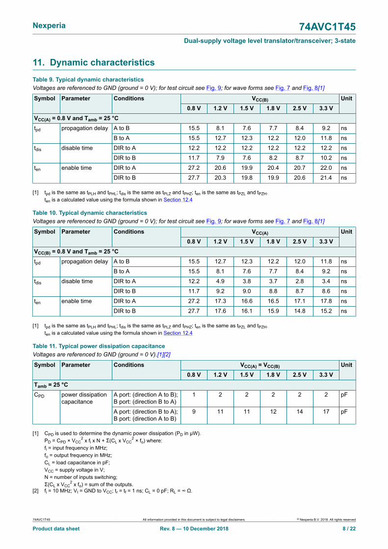
11. Dynamic characteristics
Table 9. Typical dynamic characteristicsVoltages are referenced to GND (ground = 0 V); for test circuit see Fig. 9; for wave forms see Fig. 7 and Fig. 8[1]
VCC(B)Symbol Parameter Conditions0.8 V 1.2 V 1.5 V 1.8 V 2.5 V 3.3 V
Unit
VCC(A) = 0.8 V and Tamb = 25 °CA to B 15.5 8.1 7.6 7.7 8.4 9.2 nstpd propagation delay
B to A 15.5 12.7 12.3 12.2 12.0 11.8 ns
DIR to A 12.2 12.2 12.2 12.2 12.2 12.2 nstdis disable time
DIR to B 11.7 7.9 7.6 8.2 8.7 10.2 ns
DIR to A 27.2 20.6 19.9 20.4 20.7 22.0 nsten enable time
DIR to B 27.7 20.3 19.8 19.9 20.6 21.4 ns
[1] tpd is the same as tPLH and tPHL; tdis is the same as tPLZ and tPHZ; ten is the same as tPZL and tPZH.ten is a calculated value using the formula shown in Section 12.4
Table 10. Typical dynamic characteristicsVoltages are referenced to GND (ground = 0 V); for test circuit see Fig. 9; for wave forms see Fig. 7 and Fig. 8[1]
VCC(A)Symbol Parameter Conditions0.8 V 1.2 V 1.5 V 1.8 V 2.5 V 3.3 V
Unit
VCC(B) = 0.8 V and Tamb = 25 °CA to B 15.5 12.7 12.3 12.2 12.0 11.8 nstpd propagation delay
B to A 15.5 8.1 7.6 7.7 8.4 9.2 ns
DIR to A 12.2 4.9 3.8 3.7 2.8 3.4 nstdis disable time
DIR to B 11.7 9.2 9.0 8.8 8.7 8.6 ns
DIR to A 27.2 17.3 16.6 16.5 17.1 17.8 nsten enable time
DIR to B 27.7 17.6 16.1 15.9 14.8 15.2 ns
[1] tpd is the same as tPLH and tPHL; tdis is the same as tPLZ and tPHZ; ten is the same as tPZL and tPZH.ten is a calculated value using the formula shown in Section 12.4
Table 11. Typical power dissipation capacitanceVoltages are referenced to GND (ground = 0 V).[1][2]
VCC(A) = VCC(B)Symbol Parameter Conditions0.8 V 1.2 V 1.5 V 1.8 V 2.5 V 3.3 V
Unit
Tamb = 25 °CA port: (direction A to B);B port: (direction B to A)
1 2 2 2 2 2 pFCPD power dissipationcapacitance
A port: (direction B to A);B port: (direction A to B)
9 11 11 12 14 17 pF
[1] CPD is used to determine the dynamic power dissipation (PD in μW).PD = CPD × VCC
2 x fi x N + Σ(CL x VCC2 × fo) where:
fi = input frequency in MHz;fo = output frequency in MHz;CL = load capacitance in pF;VCC = supply voltage in V;N = number of inputs switching;Σ(CL x VCC
2 x fo) = sum of the outputs.[2] fi = 10 MHz; VI = GND to VCC; tr = tf = 1 ns; CL = 0 pF; RL = ∞ Ω.
74AVC1T45 All information provided in this document is subject to legal disclaimers. © Nexperia B.V. 2018. All rights reserved
Product data sheet Rev. 8 — 10 December 2018 8 / 22

Nexperia 74AVC1T45Dual-supply voltage level translator/transceiver; 3-state
Table 12. Dynamic characteristicsVoltages are referenced to GND (ground = 0 V); for test circuit see Fig. 9; for wave forms see Fig. 7 and Fig. 8[1]
VCC(B)
1.2 V±0.1 V 1.5 V±0.1 V 1.8 V±0.15 V 2.5 V±0.2 V 3.3 V±0.3 VSymbol Parameter Conditions
Min Max Min Max Min Max Min Max Min Max
Unit
VCC(A) = 1.1 V to 1.3 V; Tamb = -40 °C to +85 °CA to B 1.0 9.0 0.7 6.8 0.6 6.1 0.5 5.7 0.5 6.1 nstpd propagation
delay B to A 1.0 9.0 0.8 8.0 0.7 7.7 0.6 7.2 0.5 7.1 ns
DIR to A 2.2 8.8 2.2 8.8 2.2 8.8 2.2 8.8 2.2 8.8 nstdis disable time
DIR to B 2.2 8.4 1.8 6.7 2.0 6.9 1.7 6.2 2.4 7.2 ns
DIR to A - 17.4 - 14.7 - 14.6 - 13.4 - 14.3 nsten enable time
DIR to B - 17.8 - 15.6 - 14.9 - 14.5 - 14.9 ns
VCC(A) = 1.4 V to 1.6 V; Tamb = -40 °C to +85 °CA to B 1.0 8.0 0.7 5.4 0.6 4.6 0.5 3.7 0.5 3.5 nstpd propagation
delay B to A 1.0 6.8 0.8 5.4 0.7 5.1 0.6 4.7 0.5 4.5 ns
DIR to A 1.6 6.3 1.6 6.3 1.6 6.3 1.6 6.3 1.6 6.3 nstdis disable time
DIR to B 2.0 7.6 1.8 5.9 1.6 6.0 1.2 4.8 1.7 5.5 ns
DIR to A - 14.4 - 11.3 - 11.1 - 9.5 - 10.0 nsten enable time
DIR to B - 14.3 - 11.7 - 10.9 - 10.0 - 9.8 ns
VCC(A) = 1.65 V to 1.95 V; Tamb = -40 °C to +85 °CA to B 1.0 7.7 0.6 5.1 0.5 4.3 0.5 3.4 0.5 3.1 nstpd propagation
delay B to A 1.0 6.1 0.7 4.6 0.5 4.4 0.5 3.9 0.5 3.7 ns
DIR to A 1.6 5.5 1.6 5.5 1.6 5.5 1.6 5.5 1.6 5.5 nstdis disable time
DIR to B 1.8 7.7 1.8 5.7 1.4 5.8 1.0 4.5 1.5 5.2 ns
DIR to A - 13.8 - 10.3 - 10.2 - 8.4 - 8.9 nsten enable time
DIR to B - 13.2 - 10.6 - 9.8 - 8.9 - 8.6 ns
VCC(A) = 2.3 V to 2.7 V; Tamb = -40 °C to +85 °CA to B 1.0 7.2 0.5 4.7 0.5 3.9 0.5 3.0 0.5 2.6 nstpd propagation
delay B to A 1.0 5.7 0.6 3.8 0.5 3.4 0.5 3.0 0.5 2.8 ns
DIR to A 1.5 4.2 1.5 4.2 1.5 4.2 1.5 4.2 1.5 4.2 nstdis disable time
DIR to B 1.7 7.3 2.0 5.2 1.5 5.1 0.6 4.2 1.1 4.8 ns
DIR to A - 13.0 - 9.0 - 8.5 - 7.2 - 7.6 nsten enable time
DIR to B - 11.4 - 8.9 - 8.1 - 7.2 - 6.8 ns
VCC(A) = 3.0 V to 3.6 V; Tamb = -40 °C to +85 °CA to B 1.0 7.1 0.5 4.5 0.5 3.7 0.5 2.8 0.5 2.4 nstpd propagation
delay B to A 1.0 6.1 0.6 3.6 0.5 3.1 0.5 2.6 0.5 2.4 ns
DIR to A 1.5 4.7 1.5 4.7 1.5 4.7 1.5 4.7 1.5 4.7 nstdis disable time
DIR to B 1.7 7.2 0.7 5.5 0.6 5.5 0.7 4.1 1.7 4.7 ns
DIR to A - 13.3 - 9.1 - 8.6 - 6.7 - 7.1 nsten enable time
DIR to B - 11.8 - 9.2 - 8.4 - 7.5 - 7.1 ns
[1] tpd is the same as tPLH and tPHL; tdis is the same as tPLZ and tPHZ; ten is the same as tPZL and tPZH. ten is a calculated value using theformula shown in Section 12.4
74AVC1T45 All information provided in this document is subject to legal disclaimers. © Nexperia B.V. 2018. All rights reserved
Product data sheet Rev. 8 — 10 December 2018 9 / 22
Nexperia 74AVC1T45Dual-supply voltage level translator/transceiver; 3-state
Table 13. Dynamic characteristicsVoltages are referenced to GND (ground = 0 V); for test circuit see Fig. 9; for wave forms see Fig. 7 and Fig. 8[1]
VCC(B)
1.2 V±0.1 V 1.5 V±0.1 V 1.8 V±0.15 V 2.5 V±0.2 V 3.3 V±0.3 VSymbol Parameter Conditions
Min Max Min Max Min Max Min Max Min Max
Unit
VCC(A) = 1.1 V to 1.3 V; Tamb = -40 °C to +125 °CA to B 1.0 9.9 0.7 7.5 0.6 6.8 0.5 6.3 0.5 6.8 nstpd propagation
delay B to A 1.0 9.9 0.8 8.8 0.7 8.5 0.6 8.0 0.5 7.9 ns
DIR to A 2.2 9.7 2.2 9.7 2.2 9.7 2.2 9.7 2.2 9.7 nstdis disable time
DIR to B 2.2 9.2 1.8 7.4 2.0 7.6 1.7 6.9 2.4 8.0 ns
DIR to A - 19.1 - 16.2 - 16.1 - 14.9 - 15.9 nsten enable time
DIR to B - 19.6 - 17.2 - 16.5 - 16.0 - 16.5 ns
VCC(A) = 1.4 V to 1.6 V; Tamb = -40 °C to +125 °CA to B 1.0 8.8 0.7 6.0 0.6 5.1 0.5 4.1 0.5 3.9 nstpd propagation
delay B to A 1.0 7.5 0.8 6.0 0.7 5.7 0.6 5.2 0.5 5.0 ns
DIR to A 1.6 7.0 1.6 7.0 1.6 7.0 1.6 7.0 1.6 7.0 nstdis disable time
DIR to B 2.0 8.3 1.8 6.5 1.6 6.6 1.2 5.3 1.7 6.1 ns
DIR to A - 15.8 - 12.5 - 12.3 - 10.5 - 11.1 nsten enable time
DIR to B - 15.8 - 13.0 - 12.1 - 11.1 - 10.9 ns
VCC(A) = 1.65 V to 1.95 V; Tamb = -40 °C to +125 °CA to B 1.0 8.5 0.6 5.7 0.5 4.8 0.5 3.8 0.5 3.5 nstpd propagation
delay B to A 1.0 6.8 0.7 5.1 0.5 4.9 0.5 4.3 0.5 4.1 ns
DIR to A 1.6 6.1 1.6 6.1 1.6 6.1 1.6 6.1 1.6 6.1 nstdis disable time
DIR to B 1.8 8.5 1.8 6.3 1.4 6.4 1.0 5.0 1.5 5.8 ns
DIR to A - 15.3 - 11.4 - 11.3 - 9.3 - 9.9 nsten enable time
DIR to B - 14.6 - 11.8 - 10.9 - 9.9 - 9.6 ns
VCC(A) = 2.3 V to 2.7 V; Tamb = -40 °C to +125 °CA to B 1.0 8.0 0.5 5.2 0.5 4.3 0.5 3.3 0.5 2.9 nstpd propagation
delay B to A 1.0 6.3 0.6 4.2 0.5 3.8 0.5 3.3 0.5 3.1 ns
DIR to A 1.5 4.7 1.5 4.7 1.5 4.7 1.5 4.7 1.5 4.7 nstdis disable time
DIR to B 1.7 8.0 2.0 5.8 1.5 5.7 0.6 4.7 1.1 5.3 ns
DIR to A - 14.3 - 10.0 - 9.5 - 8.0 - 8.4 nsten enable time
DIR to B - 12.7 - 9.9 - 9.0 - 8.0 - 7.6 ns
VCC(A) = 3.0 V to 3.6 V; Tamb = -40 °C to +125 °CA to B 1.0 7.9 0.5 5.0 0.5 4.1 0.5 3.1 0.5 2.7 nstpd propagation
delay B to A 1.0 6.8 0.6 4.0 0.5 3.5 0.5 2.9 0.5 2.7 ns
DIR to A 1.5 5.2 1.5 5.2 1.5 5.2 1.5 5.2 1.5 5.2 nstdis disable time
DIR to B 1.7 7.9 0.7 6.1 0.6 6.1 0.7 4.6 1.7 5.2 ns
DIR to A - 14.7 - 10.1 - 9.6 - 7.5 - 7.9 nsten enable time
DIR to B - 13.1 - 10.2 - 9.3 - 8.3 - 7.9 ns
[1] tpd is the same as tPLH and tPHL; tdis is the same as tPLZ and tPHZ; ten is the same as tPZL and tPZH. ten is a calculated value using theformula shown in Section 12.4
74AVC1T45 All information provided in this document is subject to legal disclaimers. © Nexperia B.V. 2018. All rights reserved
Product data sheet Rev. 8 — 10 December 2018 10 / 22
Nexperia 74AVC1T45Dual-supply voltage level translator/transceiver; 3-state
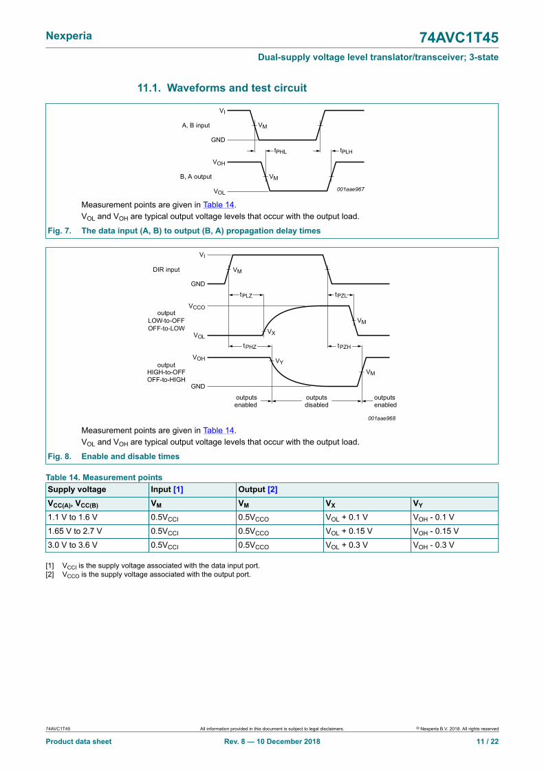
11.1. Waveforms and test circuit
001aae967
A, B input
B, A output
tPLHtPHL
GND
VI
VOH
VM
VM
VOL
Measurement points are given in Table 14.VOL and VOH are typical output voltage levels that occur with the output load.
Fig. 7. The data input (A, B) to output (B, A) propagation delay times
001aae968
tPZL
tPZHtPHZ
tPLZ
GND
GND
VI
VCCO
VOL
VOH
VM
VM
VM
VX
VY
outputs disabled
outputs enabled
outputs enabled
output LOW-to-OFF OFF-to-LOW
output HIGH-to-OFF OFF-to-HIGH
DIR input
Measurement points are given in Table 14.VOL and VOH are typical output voltage levels that occur with the output load.
Fig. 8. Enable and disable times
Table 14. Measurement pointsSupply voltage Input [1] Output [2]VCC(A), VCC(B) VM VM VX VY
1.1 V to 1.6 V 0.5VCCI 0.5VCCO VOL + 0.1 V VOH - 0.1 V
1.65 V to 2.7 V 0.5VCCI 0.5VCCO VOL + 0.15 V VOH - 0.15 V
3.0 V to 3.6 V 0.5VCCI 0.5VCCO VOL + 0.3 V VOH - 0.3 V
[1] VCCI is the supply voltage associated with the data input port.[2] VCCO is the supply voltage associated with the output port.
74AVC1T45 All information provided in this document is subject to legal disclaimers. © Nexperia B.V. 2018. All rights reserved
Product data sheet Rev. 8 — 10 December 2018 11 / 22
Nexperia 74AVC1T45Dual-supply voltage level translator/transceiver; 3-state
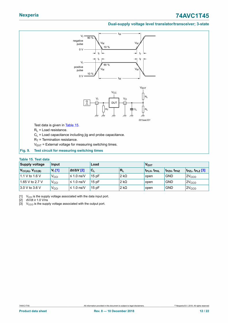
VM VM
tW
tW
10 %
90 %
0 V
VI
VI
negative pulse
positive pulse
0 V
VM VM
90 %
10 %
tf
tr
tr
tf
001aae331
VEXT
VCC
VI VODUT
CLRT
RL
RL
G
Test data is given in Table 15.RL = Load resistance.CL = Load capacitance including jig and probe capacitance.RT = Termination resistance.VEXT = External voltage for measuring switching times.
Fig. 9. Test circuit for measuring switching times
Table 15. Test dataSupply voltage Input Load VEXT
VCC(A), VCC(B) VI [1] Δt/ΔV [2] CL RL tPLH, tPHL tPZH, tPHZ tPZL, tPLZ [3]1.1 V to 1.6 V VCCI ≤ 1.0 ns/V 15 pF 2 kΩ open GND 2VCCO
1.65 V to 2.7 V VCCI ≤ 1.0 ns/V 15 pF 2 kΩ open GND 2VCCO
3.0 V to 3.6 V VCCI ≤ 1.0 ns/V 15 pF 2 kΩ open GND 2VCCO
[1] VCCI is the supply voltage associated with the data input port.[2] dV/dt ≥ 1.0 V/ns[3] VCCO is the supply voltage associated with the output port.
74AVC1T45 All information provided in this document is subject to legal disclaimers. © Nexperia B.V. 2018. All rights reserved
Product data sheet Rev. 8 — 10 December 2018 12 / 22
Nexperia 74AVC1T45Dual-supply voltage level translator/transceiver; 3-state
12. Application information
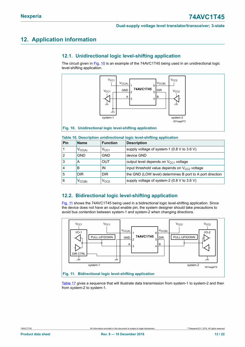
12.1. Unidirectional logic level-shifting applicationThe circuit given in Fig. 10 is an example of the 74AVC1T45 being used in an unidirectional logiclevel-shifting application.
001aag973
74AVC1T451
VCC(A)
2GND
3
6
5
4A
VCC(B)
VCC2
VCC2
DIR
system-2system-1
B
VCC1
VCC1
Fig. 10. Unidirectional logic level-shifting application
Table 16. Description unidirectional logic level-shifting applicationPin Name Function Description1 VCC(A) VCC1 supply voltage of system-1 (0.8 V to 3.6 V)
2 GND GND device GND
3 A OUT output level depends on VCC1 voltage
4 B IN input threshold value depends on VCC2 voltage
5 DIR DIR the GND (LOW level) determines B port to A port direction
6 VCC(B) VCC2 supply voltage of system-2 (0.8 V to 3.6 V)
12.2. Bidirectional logic level-shifting applicationFig. 11 shows the 74AVC1T45 being used in a bidirectional logic level-shifting application. Sincethe device does not have an output enable pin, the system designer should take precautions toavoid bus contention between system-1 and system-2 when changing directions.
001aag974
DIR CTRL
I/O-1
VCC1
I/O-274AVC1T45
1VCC(A)
VCC1 VCC2
2GND
3
6
5
4A
VCC(B)
DIR
B
PULL-UP/DOWN
system-1 system-2
PULL-UP/DOWN
VCC2
Fig. 11. Bidirectional logic level-shifting application
Table 17 gives a sequence that will illustrate data transmission from system-1 to system-2 and thenfrom system-2 to system-1.
74AVC1T45 All information provided in this document is subject to legal disclaimers. © Nexperia B.V. 2018. All rights reserved
Product data sheet Rev. 8 — 10 December 2018 13 / 22

Nexperia 74AVC1T45Dual-supply voltage level translator/transceiver; 3-state
Table 17. Description bidirectional logic level-shifting applicationH = HIGH voltage level; L = LOW voltage level; Z = high-impedance OFF-state.
State DIR CTRL I/O-1 I/O-2 Description1 H output input system-1 data to system-2
2 H Z Z system-2 is getting ready to send data to system-1.I/O-1 and I/O-2 are disabled. The bus-line state dependson bus hold.
3 L Z Z DIR bit is set LOW. I/O-1 and I/O-2 still are disabled. Thebus-line state depends on bus hold.
4 L input output system-2 data to system-1
12.3. Power-up considerationsThe device is designed such that no special power-up sequence is required other than GND beingapplied first.
Table 18. Typical total supply current (ICC(A) + ICC(B))VCC(B)VCC(A)
0 V 0.8 V 1.2 V 1.5 V 1.8 V 2.5 V 3.3 VUnit
0 V 0 0.1 0.1 0.1 0.1 0.1 0.1 μA
0.8 V 0.1 0.1 0.1 0.1 0.1 0.7 2.3 μA
1.2 V 0.1 0.1 0.1 0.1 0.1 0.3 1.4 μA
1.5 V 0.1 0.1 0.1 0.1 0.1 0.1 0.9 μA
1.8 V 0.1 0.1 0.1 0.1 0.1 0.1 0.5 μA
2.5 V 0.1 0.7 0.3 0.1 0.1 0.1 0.1 μA
3.3 V 0.1 2.3 1.4 0.9 0.5 0.1 0.1 μA
12.4. Enable timesCalculate the enable times for the 74AVC1T45 using the following formulas:
• ten (DIR to A) = tdis (DIR to B) + tpd (B to A)• ten (DIR to B) = tdis (DIR to A) + tpd (A to B)
In a bidirectional application, these enable times provide the maximum delay from the timethe DIR bit is switched until an output is expected. For example, if the 74AVC1T45 initially istransmitting from A to B, then the DIR bit is switched, the B port of the device must be disabledbefore presenting it with an input. After the B port has been disabled, an input signal applied to itappears on the corresponding A port after the specified propagation delay.
74AVC1T45 All information provided in this document is subject to legal disclaimers. © Nexperia B.V. 2018. All rights reserved
Product data sheet Rev. 8 — 10 December 2018 14 / 22

Nexperia 74AVC1T45Dual-supply voltage level translator/transceiver; 3-state
13. Package outline
REFERENCESOUTLINE VERSION
EUROPEAN PROJECTION ISSUE DATE
IEC JEDEC JEITA
SOT363 SC-88
w BMbp
D
e1
e
pin 1 index A
A1
Lp
Q
detail X
HE
E
v M A
AB
y
0 1 2 mm
scale
c
X
1 32
456
Plastic surface-mounted package; 6 leads SOT363
UNITA1
maxbp c D E e1 HE Lp Q ywv
mm 0.1 0.30 0.20
2.2 1.8
0.25 0.10
1.35 1.15 0.65
e
1.3 2.2 2.0 0.2 0.10.2
DIMENSIONS (mm are the original dimensions)
0.45 0.15
0.25 0.15
A
1.1 0.8
04-11-08 06-03-16
Fig. 12. Package outline SOT363 (SC-88)
74AVC1T45 All information provided in this document is subject to legal disclaimers. © Nexperia B.V. 2018. All rights reserved
Product data sheet Rev. 8 — 10 December 2018 15 / 22
Nexperia 74AVC1T45Dual-supply voltage level translator/transceiver; 3-state
ReferencesOutlineversion
Europeanprojection Issue date
IEC JEDEC JEITA
SOT886 MO-252
sot886_po
04-07-2212-01-05
Unit
mmmaxnommin
0.5 0.04 1.501.451.40
1.051.000.95
0.350.300.27
0.400.350.32
0.6
A(1)
Dimensions (mm are the original dimensions)
Notes1. Including plating thickness.2. Can be visible in some manufacturing processes.
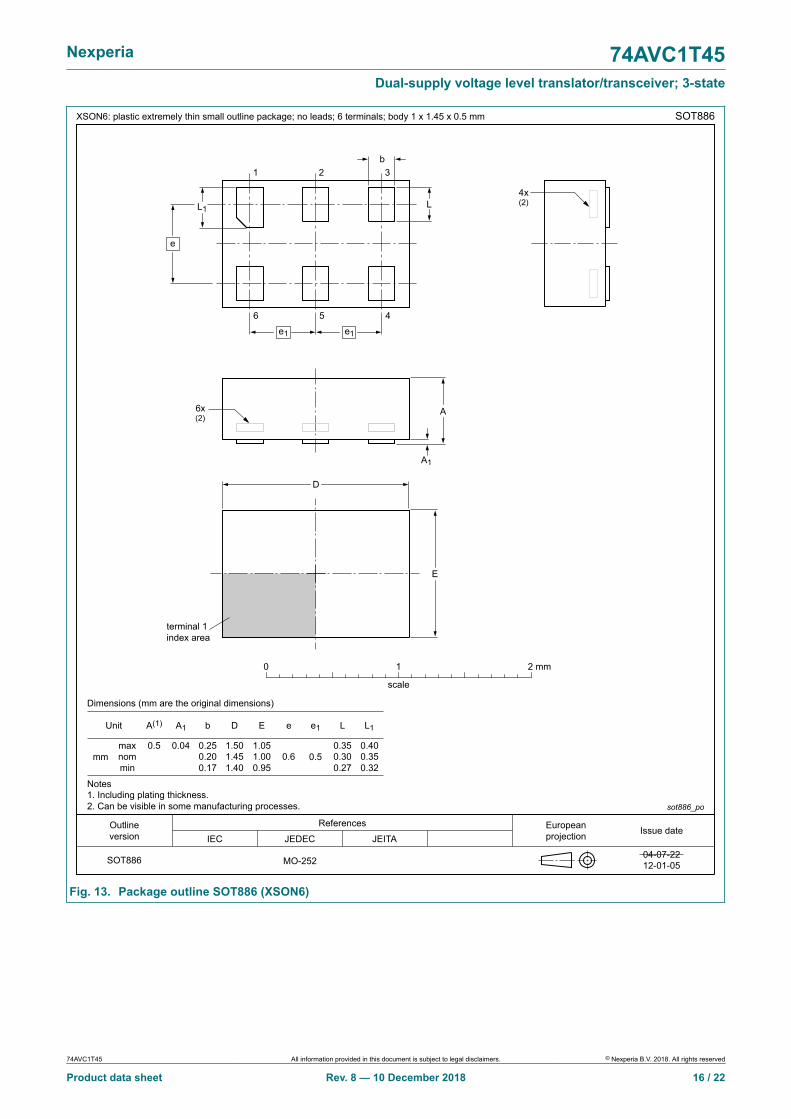
XSON6: plastic extremely thin small outline package; no leads; 6 terminals; body 1 x 1.45 x 0.5 mm SOT886
A1 b
0.250.200.17
D E e e1
0.5
L L1
terminal 1index area
D
E
e1
e
A1
b
LL1
e1
0 1 2 mm
scale
1
6
2
5
3
4
6x(2)
4x(2)
A
Fig. 13. Package outline SOT886 (XSON6)
74AVC1T45 All information provided in this document is subject to legal disclaimers. © Nexperia B.V. 2018. All rights reserved
Product data sheet Rev. 8 — 10 December 2018 16 / 22
Nexperia 74AVC1T45Dual-supply voltage level translator/transceiver; 3-state
ReferencesOutline version
European projection Issue date
IEC JEDEC JEITA
SOT1115
sot1115_po
10-04-02 10-04-07
Unit
mmmax nom min
0.35 0.04 0.95 0.90 0.85
1.05 1.00 0.95
0.55 0.30.40 0.35 0.32
A(1)
Dimensions
Note 1. Including plating thickness. 2. Visible depending upon used manufacturing technology.
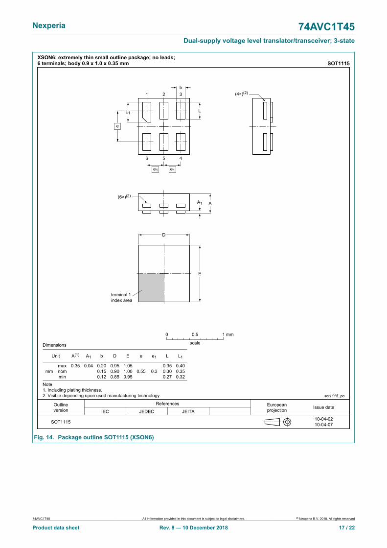
XSON6: extremely thin small outline package; no leads; 6 terminals; body 0.9 x 1.0 x 0.35 mm SOT1115
A1 b
0.20 0.15 0.12
D E e e1 L
0.35 0.30 0.27
L1
0 0.5 1 mm
scale
terminal 1 index area
D
E
(4×)(2)
e1 e1
e
LL1
b321
6 5 4
(6×)(2)
A1 A
Fig. 14. Package outline SOT1115 (XSON6)
74AVC1T45 All information provided in this document is subject to legal disclaimers. © Nexperia B.V. 2018. All rights reserved
Product data sheet Rev. 8 — 10 December 2018 17 / 22

Nexperia 74AVC1T45Dual-supply voltage level translator/transceiver; 3-state
ReferencesOutline version
European projection Issue date
IEC JEDEC JEITA
SOT1202
sot1202_po
10-04-02 10-04-06
Unit
mmmax nom min
0.35 0.04 1.05 1.00 0.95
1.05 1.00 0.95
0.55 0.350.40 0.35 0.32
A(1)
Dimensions
Note 1. Including plating thickness. 2. Visible depending upon used manufacturing technology.
XSON6: extremely thin small outline package; no leads; 6 terminals; body 1.0 x 1.0 x 0.35 mm SOT1202
A1 b
0.20 0.15 0.12
D E e e1 L
0.35 0.30 0.27
L1
0 0.5 1 mm
scale
terminal 1 index area
D
E
(4×)(2)
e1 e1
e
L
b1 2 3
L1
6 5 4
(6×)(2)
AA1
Fig. 15. Package outline SOT1202 (XSON6)
74AVC1T45 All information provided in this document is subject to legal disclaimers. © Nexperia B.V. 2018. All rights reserved
Product data sheet Rev. 8 — 10 December 2018 18 / 22

Nexperia 74AVC1T45Dual-supply voltage level translator/transceiver; 3-state
ReferencesOutlineversion
Europeanprojection Issue date
IEC JEDEC JEITA
SOT1255
sot1255_po
15-07-2015-07-22
Unit
mmmaxnommin
0.35 0.04 0.30 0.850.20 0.10 0.05
A
Dimensions (mm are the original dimensions)
X2SON6: plastic thermal enhanced extremely thin small outline package; no leads;6 terminals; body 1.0 x 0.8 x 0.35 mm SOT1255
A1 D
1.05
Dh E e1 e2 b
0.25
L v y
0.05
y1
0.32 0.02 0.25 0.80 0.60 0.401.000.170.220.30 0.00 0.22 0.750.95
0.250.30
0 1 mm
scale
A B
pin 1ID area
X
L(4x)
e1
1 6
Dh(2x)
3 4
52
e2
A Bv
D
E
C
yCy1
detail X
A
A1
b(4x)
Fig. 16. Package outline SOT1255 (X2SON6)
74AVC1T45 All information provided in this document is subject to legal disclaimers. © Nexperia B.V. 2018. All rights reserved
Product data sheet Rev. 8 — 10 December 2018 19 / 22
Nexperia 74AVC1T45Dual-supply voltage level translator/transceiver; 3-state
14. Abbreviations
Table 19. AbbreviationsAcronym DescriptionCDM Charged Device Model
CMOS Complementary Metal Oxide Semiconductor
DUT Device Under Test
ESD ElectroStatic Discharge
HBM Human Body Model
MM Machine Model
15. Revision history
Table 20. Revision historyDocument ID Release date Data sheet status Change notice Supersedes74AVC1T45 v.8 20181210 Product data sheet - 74AVC1T45 v.7
74AVC1T45 v.7 20170824 Product data sheet - 74AVC1T45 v.6
Modifications: • The format of this data sheet has been redesigned to comply with the identity guidelines ofNexperia.
• Legal texts have been adapted to the new company name where appropriate.
74AVC1T45 v.6 20160420 Product data sheet - 74AVC1T45 v.5
Modifications: • Added type number 74AVC1T45GX(SOT1255/X2SON6 package).
74AVC1T45 v.5 20160106 Product data sheet - 74AVC1T45 v.4
Modifications: • Table 16: Labels for pins 4 and 5 corrected.
74AVC1T45 v.4 20120622 Product data sheet - 74AVC1T45 v.3
Modifications: • Package outline drawing of SOT886 (Fig. 13) modified.
74AVC1T45 v.3 20111021 Product data sheet - 74AVC1T45 v.2
Modifications: • Added type number 74AVC1T45GN (SOT1115/XSON6 package).• Added type number 74AVC1T45GS (SOT1202/XSON6 package).
74AVC1T45 v.2 20090505 Product data sheet - 74AVC1T45 v.1
74AVC1T45 v.1 20080118 Product data sheet - -
74AVC1T45 All information provided in this document is subject to legal disclaimers. © Nexperia B.V. 2018. All rights reserved
Product data sheet Rev. 8 — 10 December 2018 20 / 22
Nexperia 74AVC1T45Dual-supply voltage level translator/transceiver; 3-state
16. Legal information
Data sheet status
Document status[1][2]
Productstatus [3]
Definition
Objective [short]data sheet
Development This document contains data fromthe objective specification forproduct development.
Preliminary [short]data sheet
Qualification This document contains data fromthe preliminary specification.
Product [short]data sheet
Production This document contains the productspecification.
[1] Please consult the most recently issued document before initiating orcompleting a design.
[2] The term 'short data sheet' is explained in section "Definitions".[3] The product status of device(s) described in this document may have
changed since this document was published and may differ in case ofmultiple devices. The latest product status information is available onthe internet at https://www.nexperia.com.
DefinitionsDraft — The document is a draft version only. The content is still underinternal review and subject to formal approval, which may result inmodifications or additions. Nexperia does not give any representations orwarranties as to the accuracy or completeness of information included hereinand shall have no liability for the consequences of use of such information.
Short data sheet — A short data sheet is an extract from a full data sheetwith the same product type number(s) and title. A short data sheet isintended for quick reference only and should not be relied upon to containdetailed and full information. For detailed and full information see the relevantfull data sheet, which is available on request via the local Nexperia salesoffice. In case of any inconsistency or conflict with the short data sheet, thefull data sheet shall prevail.
Product specification — The information and data provided in a Productdata sheet shall define the specification of the product as agreed betweenNexperia and its customer, unless Nexperia and customer have explicitlyagreed otherwise in writing. In no event however, shall an agreement bevalid in which the Nexperia product is deemed to offer functions and qualitiesbeyond those described in the Product data sheet.
DisclaimersLimited warranty and liability — Information in this document is believedto be accurate and reliable. However, Nexperia does not give anyrepresentations or warranties, expressed or implied, as to the accuracyor completeness of such information and shall have no liability for theconsequences of use of such information. Nexperia takes no responsibilityfor the content in this document if provided by an information source outsideof Nexperia.
In no event shall Nexperia be liable for any indirect, incidental, punitive,special or consequential damages (including - without limitation - lostprofits, lost savings, business interruption, costs related to the removalor replacement of any products or rework charges) whether or not suchdamages are based on tort (including negligence), warranty, breach ofcontract or any other legal theory.
Notwithstanding any damages that customer might incur for any reasonwhatsoever, Nexperia’s aggregate and cumulative liability towards customerfor the products described herein shall be limited in accordance with theTerms and conditions of commercial sale of Nexperia.
Right to make changes — Nexperia reserves the right to make changesto information published in this document, including without limitationspecifications and product descriptions, at any time and without notice. Thisdocument supersedes and replaces all information supplied prior to thepublication hereof.
Suitability for use — Nexperia products are not designed, authorized orwarranted to be suitable for use in life support, life-critical or safety-criticalsystems or equipment, nor in applications where failure or malfunctionof an Nexperia product can reasonably be expected to result in personal
injury, death or severe property or environmental damage. Nexperia and itssuppliers accept no liability for inclusion and/or use of Nexperia products insuch equipment or applications and therefore such inclusion and/or use is atthe customer’s own risk.
Quick reference data — The Quick reference data is an extract of theproduct data given in the Limiting values and Characteristics sections of thisdocument, and as such is not complete, exhaustive or legally binding.
Applications — Applications that are described herein for any of theseproducts are for illustrative purposes only. Nexperia makes no representationor warranty that such applications will be suitable for the specified usewithout further testing or modification.
Customers are responsible for the design and operation of their applicationsand products using Nexperia products, and Nexperia accepts no liability forany assistance with applications or customer product design. It is customer’ssole responsibility to determine whether the Nexperia product is suitableand fit for the customer’s applications and products planned, as well asfor the planned application and use of customer’s third party customer(s).Customers should provide appropriate design and operating safeguards tominimize the risks associated with their applications and products.
Nexperia does not accept any liability related to any default, damage, costsor problem which is based on any weakness or default in the customer’sapplications or products, or the application or use by customer’s third partycustomer(s). Customer is responsible for doing all necessary testing for thecustomer’s applications and products using Nexperia products in order toavoid a default of the applications and the products or of the application oruse by customer’s third party customer(s). Nexperia does not accept anyliability in this respect.
Limiting values — Stress above one or more limiting values (as defined inthe Absolute Maximum Ratings System of IEC 60134) will cause permanentdamage to the device. Limiting values are stress ratings only and (proper)operation of the device at these or any other conditions above thosegiven in the Recommended operating conditions section (if present) or theCharacteristics sections of this document is not warranted. Constant orrepeated exposure to limiting values will permanently and irreversibly affectthe quality and reliability of the device.
Terms and conditions of commercial sale — Nexperia products aresold subject to the general terms and conditions of commercial sale, aspublished at http://www.nexperia.com/profile/terms, unless otherwise agreedin a valid written individual agreement. In case an individual agreement isconcluded only the terms and conditions of the respective agreement shallapply. Nexperia hereby expressly objects to applying the customer’s generalterms and conditions with regard to the purchase of Nexperia products bycustomer.
No offer to sell or license — Nothing in this document may be interpretedor construed as an offer to sell products that is open for acceptance or thegrant, conveyance or implication of any license under any copyrights, patentsor other industrial or intellectual property rights.
Export control — This document as well as the item(s) described hereinmay be subject to export control regulations. Export might require a priorauthorization from competent authorities.
Non-automotive qualified products — Unless this data sheet expresslystates that this specific Nexperia product is automotive qualified, theproduct is not suitable for automotive use. It is neither qualified nor tested inaccordance with automotive testing or application requirements. Nexperiaaccepts no liability for inclusion and/or use of non-automotive qualifiedproducts in automotive equipment or applications.
In the event that customer uses the product for design-in and use inautomotive applications to automotive specifications and standards,customer (a) shall use the product without Nexperia’s warranty of theproduct for such automotive applications, use and specifications, and (b)whenever customer uses the product for automotive applications beyondNexperia’s specifications such use shall be solely at customer’s own risk,and (c) customer fully indemnifies Nexperia for any liability, damages or failedproduct claims resulting from customer design and use of the product forautomotive applications beyond Nexperia’s standard warranty and Nexperia’sproduct specifications.
Translations — A non-English (translated) version of a document is forreference only. The English version shall prevail in case of any discrepancybetween the translated and English versions.
TrademarksNotice: All referenced brands, product names, service names andtrademarks are the property of their respective owners.
74AVC1T45 All information provided in this document is subject to legal disclaimers. © Nexperia B.V. 2018. All rights reserved
Product data sheet Rev. 8 — 10 December 2018 21 / 22
Nexperia 74AVC1T45Dual-supply voltage level translator/transceiver; 3-state
Contents
1. General description......................................................12. Features and benefits.................................................. 13. Ordering information....................................................24. Marking.......................................................................... 25. Functional diagram.......................................................26. Pinning information......................................................36.1. Pinning.........................................................................36.2. Pin description............................................................. 37. Functional description................................................. 48. Limiting values............................................................. 49. Recommended operating conditions..........................510. Static characteristics..................................................511. Dynamic characteristics.............................................811.1. Waveforms and test circuit.......................................1112. Application information........................................... 1312.1. Unidirectional logic level-shifting application............1312.2. Bidirectional logic level-shifting application.............. 1312.3. Power-up considerations......................................... 1412.4. Enable times............................................................1413. Package outline........................................................ 1514. Abbreviations............................................................2015. Revision history........................................................2016. Legal information......................................................21
© Nexperia B.V. 2018. All rights reservedFor more information, please visit: http://www.nexperia.comFor sales office addresses, please send an email to: [email protected] of release: 10 December 2018
74AVC1T45 All information provided in this document is subject to legal disclaimers. © Nexperia B.V. 2018. All rights reserved
Product data sheet Rev. 8 — 10 December 2018 22 / 22

![· 430 mhz fm mobile transceiver dj-520j dual band fm handy transceiver dj-530j 144/430mhz dual band fm handy transceiver . r 10f3 r 10173] (tcxo) (tcxo) digital ej-47u ¥14,800](https://img.pdfslide.us/doc/110x75/604c0c10cc37c0411e3ddecf/430-mhz-fm-mobile-transceiver-dj-520j-dual-band-fm-handy-transceiver-dj-530j-144430mhz.jpg)