Embed Size (px)
Citation preview
RT8167B
1DS8167B-00 October 2011 www.richtek.com
General DescriptionThe RT8167B is a dual single-phase PWM controller withintegrated MOSFET drivers, compliant with Intel IMVP7Pulse Width Modulation Specification to support bothCPU core and GPU core power. This part adopts G-NAVPTM
(Green-Native AVP), which is a Richtek proprietary topologyderived from finite DC gain compensator in constant on-time control mode. G-NAVPTM makes this part an easysetting PWM controller to meet all Intel AVP (ActiveVoltage Positioning) mobile CPU/GPU requirements. TheRT8167B uses SVID interface to control an 8-bit DAC foroutput voltage programming. The built-in high accuracyDAC converts the received VID code into a voltage valueranging from 0V to 1.52V with 5mV step voltage. Thesystem accuracy of the controller can reach 0.8%. TheRT8167B operates in continuous conduction mode ordiode emulation mode, according to the SVID command.The maximum efficiency can reach up to 90% in differentoperating modes according to different load conditions.The droop function (load line) can be easily programmedby setting the DC gain of the error amplifier. With propercompensation, the load transient response can achieveoptimized AVP performance.
The output voltage transition slew rate is set via the SVIDinterface. The RT8167B supports both DCR and senseresistor current sensing. The RT8167B providesVR_READY and thermal throttling output signals forIMVP7 CPU and GPU core. This part also featurescomplete fault protection functions including over voltage,under voltage, negative voltage, over current and thermalshutdown.
The RT8167B is available in a WQFN-40L 5x5 smallfootprint package.
Dual Single-Phase PWM Controller for CPU and GPU CorePower Supply
ApplicationsIMVP7 Intel CPU/GPU Core Power SupplyLaptop ComputersAVP Step-Down Converter
FeaturesDual Single-Phase PWM Controller for CPU Coreand GPU Core PowerIMVP7 Compatible Power Management StatesSerial VID InterfaceG-NAVPTM TopologyAVP for CPU VR Only0.5% DAC Accuracy0.8% System AccuracyDifferential Remote Voltage SensingBuilt-in ADC for Platform Programming
SETINI/SETINIA for CPU/GPU Core VR InitialStartup VoltageTMPMAX to Set Platform Maximum TemperatureICCMAX/ICCMAXA for CPU/GPU Core VRMaximum Current
Power Good Indicator : VR_READY/VRA_READY forCPU/GPU Core PowerThermal Throttling Indicator : VRHOTDiode Emulation Mode at Light Load ConditionFast Line/Load Transient ResponseSwitching Frequency up to 1MHz per PhaseOVP, UVP, NVP, OTP, UVLO, OCPSmall 40-Lead WQFN PackageRoHS Compliant and Halogen Free
RT8167B
2DS8167B-00 October 2011www.richtek.com
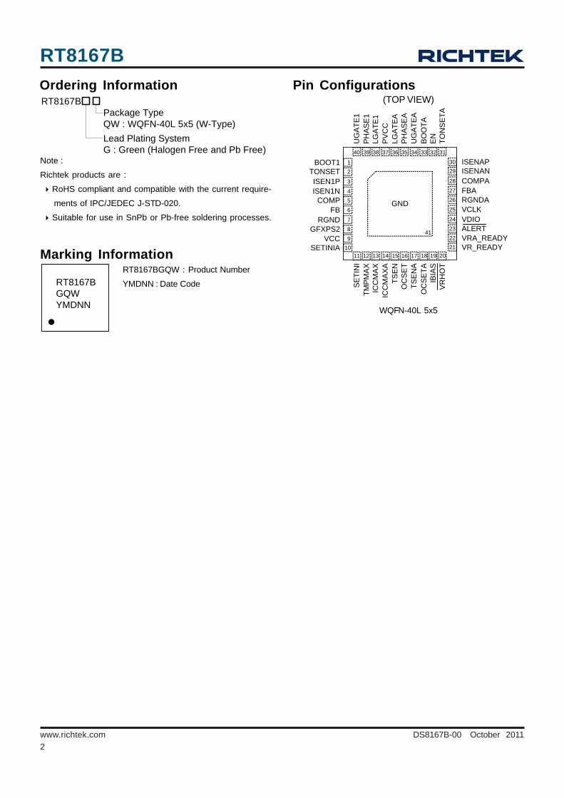
Ordering Information
Note :
Richtek products are :
RoHS compliant and compatible with the current require-
ments of IPC/JEDEC J-STD-020.
Suitable for use in SnPb or Pb-free soldering processes.
Pin Configurations(TOP VIEW)
WQFN-40L 5x5
BOOT1
ISEN1NISEN1P
SETINIAVCC
GFXPS2RGND
COMPFB
TONSETISENAP
FBACOMPA
VR_READYVRA_READY
VDIO
RGNDAVCLK
ISENAN12
3
45
6
789
10
3029
28
2726
25
24232221
SETI
NI
TMPM
AXIC
CM
AXIC
CM
AXA
TSE
NO
CSE
TTS
EN
AO
CSE
TAIB
IAS
UG
ATE
1PH
ASE
1LG
ATE1
PVC
CLG
ATEA
PHAS
EA
UG
ATE
ABO
OTA
EN TON
SE
TA
20191817161514131211
31323334353637383940
41
GND
VRH
OT
ALERT
Marking Information
Package TypeQW : WQFN-40L 5x5 (W-Type)
RT8167B
Lead Plating SystemG : Green (Halogen Free and Pb Free)
RT8167BGQWYMDNN
RT8167BGQW : Product Number
YMDNN : Date Code
RT8167B
3DS8167B-00 October 2011 www.richtek.com
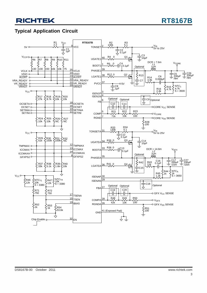
Typical Application Circuit
VCORE
40
39
38
32
2
ISEN1N
RT8167B
EN
TONSET
1
VCC
ISEN1P3
L1
VIN
C3
R14 C6C5
C1
C4
Q1
R5
R4
R13
C7
9
GND41 (Exposed Pad)
R2
COMP
FB
R21
C11C10CORE VCC SENSE
R23
C9
PVCCC8
37
R1
5V
6
5
4
RGND 7
C2
R3
Q2R12
NTC1R15
R28
34
35
36
31
ISENAN
TONSETA
ISENAP 30
L2
VIN
C14
R43 C16 C17
R35
5V to 25V
R42
C15
R33
COMPA
FBA
R48
C20C19
R50
C1827
28
29
RGNDA 26
C12
R34
Q4R41
NTCAR44
R51
25 VCLKVCLK24 VDIOVDIO23ALERT
R8R7R6VCCP
22 VRA_READYVRA_READY21 VR_READYVR_READY
R9 R10 R11
VRHOT 20
18 OCSETA
R17
VCC
1610 SETINIA
R18 R19 R20
SETINI11
R25 R26 R27R24
OCSETOCSETA
SETINIASETINI
OCSET
8 GFXPS2
VCC
1213 ICCMAX
R29 R30 R31
ICCMAXA14
R37 R38 R39
TMPMAXICCMAX
TMPMAX
IBIAS19
R54
R47NTCT1R46
TSENATSEN15
17
NTCTA
VCC
R16
R22
R45
R52 R53
R49
5V
VCC
BOOT1
VGFX
VGFX
R32
R40
ALERT
VRHOT
UGATEA
PHASEA
LGATEA
5V to 25V
UGATE1
PHASE1
LGATE1
Chip Enable
GFX VCC SENSE
GFX VSS SENSE
33 C13
Q3
BOOTAR36
CORE VSS SENSE
VCORE
GFXPS2ICCMAXA
2.2
1µF
130 130 150 10k10k 75
27k 8.7k 10k 10k
10k10k NC NC
51k 150k 100k NC
33k 5.1k 1.6k 10k
12k 10kß = 3380
12k10kß = 3380
R71750
R72750
1k 1k53.6k
130k
0.1µF
5.1
10µF0
00.1µF 1µH
DCR = 7.6m
Optional
3.9k 0.068µF
2.4k4.7k 4.7k
ß = 3500
330µF/9m
C26330µF/9m
Optional Optional
71k 10k 100
100
Optional
0
1µF
130k 5.1
0.1µF
10µF0
00.1µF
0
Optional
11k 0.1µF
1.2k1k 1k
ß = 3650
330µF/15m
C27330µF/15m
OptionalOptional Optional
42k 10k 100
100
2µH
DCR = 14.6m
RT8167B
4DS8167B-00 October 2011www.richtek.com
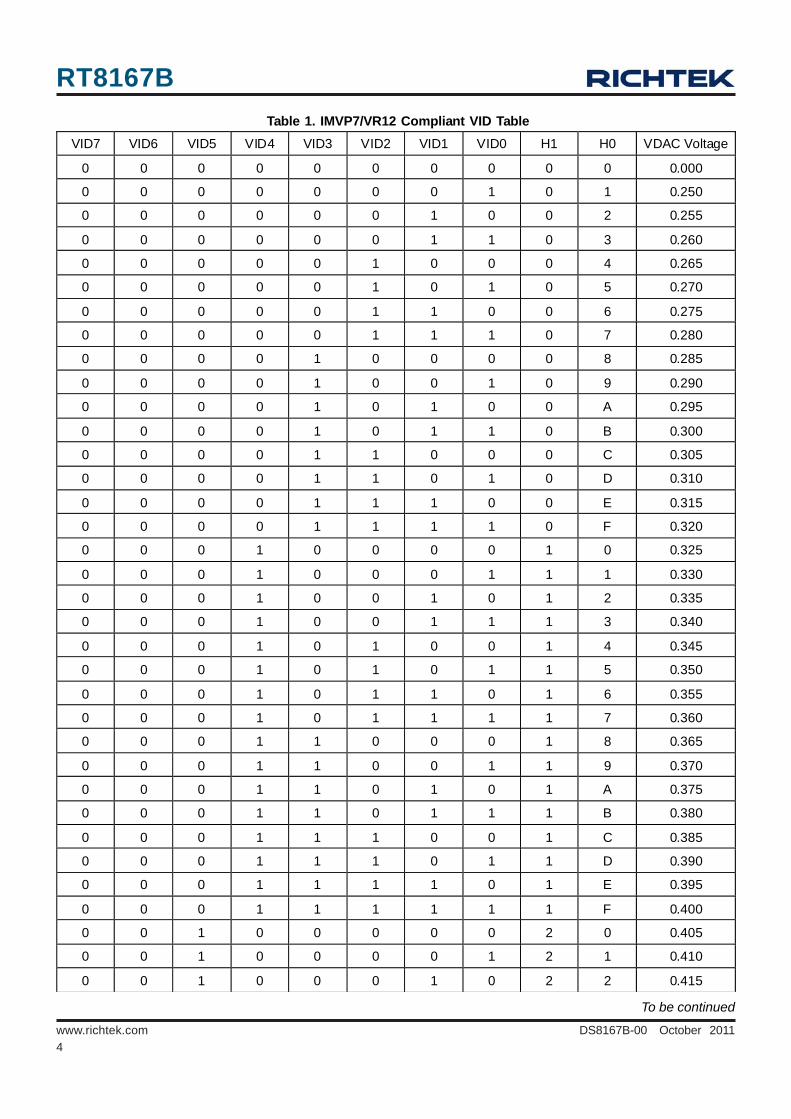
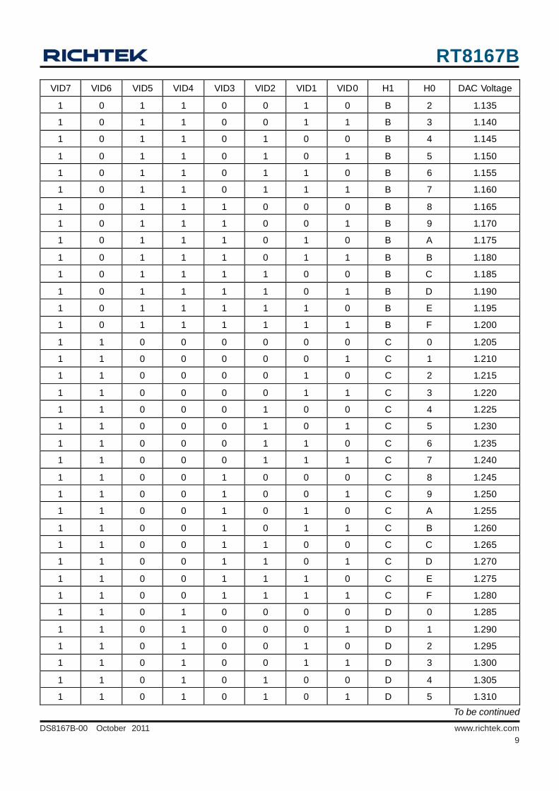
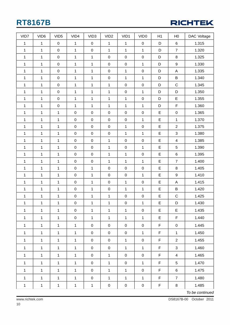
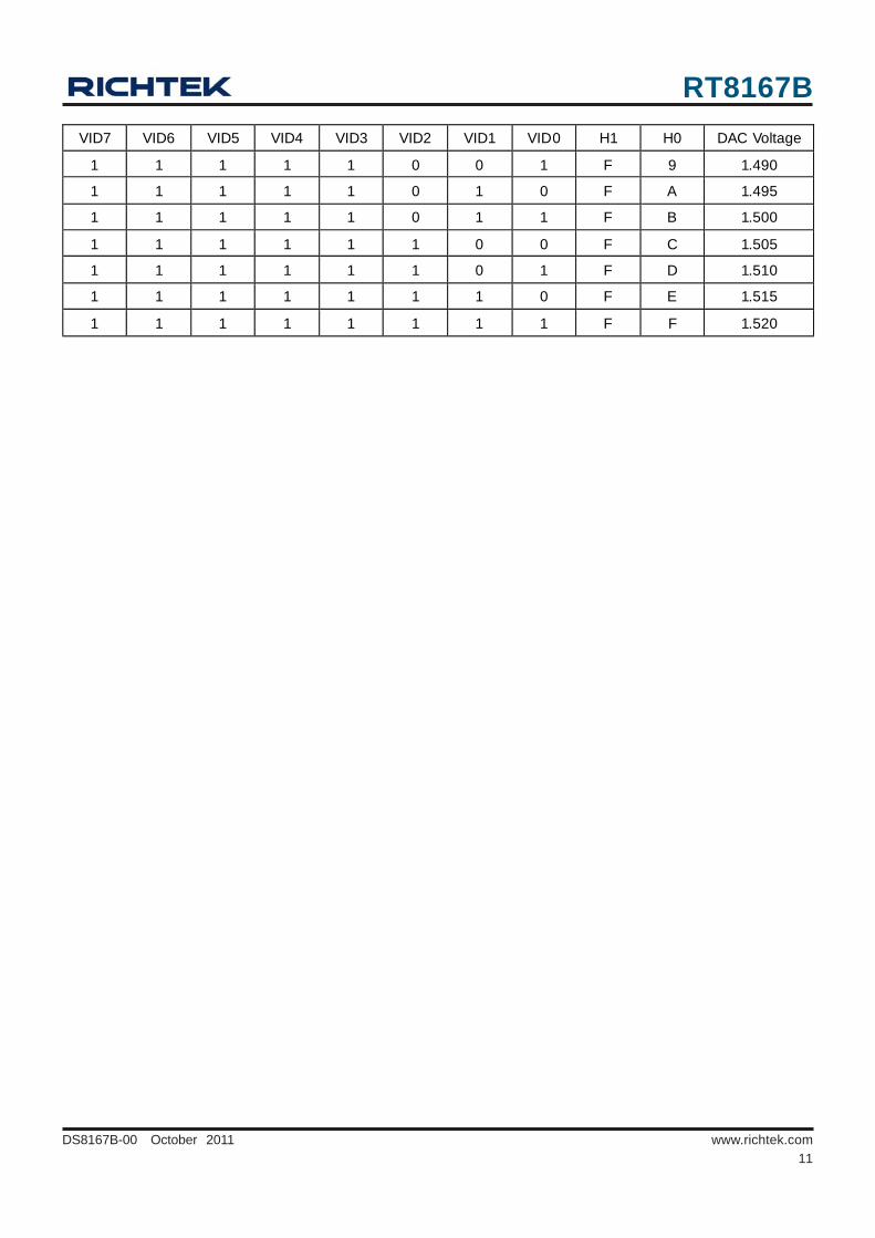
VID7 VID6 VID5 VID4 VID3 VID2 VID1 VID0 H1 H0 VDAC Voltage
0 0 0 0 0 0 0 0 0 0 0.000
0 0 0 0 0 0 0 1 0 1 0.250
0 0 0 0 0 0 1 0 0 2 0.255
0 0 0 0 0 0 1 1 0 3 0.260
0 0 0 0 0 1 0 0 0 4 0.265
0 0 0 0 0 1 0 1 0 5 0.270
0 0 0 0 0 1 1 0 0 6 0.275
0 0 0 0 0 1 1 1 0 7 0.280
0 0 0 0 1 0 0 0 0 8 0.285
0 0 0 0 1 0 0 1 0 9 0.290
0 0 0 0 1 0 1 0 0 A 0.295
0 0 0 0 1 0 1 1 0 B 0.300
0 0 0 0 1 1 0 0 0 C 0.305
0 0 0 0 1 1 0 1 0 D 0.310
0 0 0 0 1 1 1 0 0 E 0.315
0 0 0 0 1 1 1 1 0 F 0.320
0 0 0 1 0 0 0 0 1 0 0.325
0 0 0 1 0 0 0 1 1 1 0.330
0 0 0 1 0 0 1 0 1 2 0.335
0 0 0 1 0 0 1 1 1 3 0.340
0 0 0 1 0 1 0 0 1 4 0.345
0 0 0 1 0 1 0 1 1 5 0.350
0 0 0 1 0 1 1 0 1 6 0.355
0 0 0 1 0 1 1 1 1 7 0.360
0 0 0 1 1 0 0 0 1 8 0.365
0 0 0 1 1 0 0 1 1 9 0.370
0 0 0 1 1 0 1 0 1 A 0.375
0 0 0 1 1 0 1 1 1 B 0.380
0 0 0 1 1 1 0 0 1 C 0.385
0 0 0 1 1 1 0 1 1 D 0.390
0 0 0 1 1 1 1 0 1 E 0.395
0 0 0 1 1 1 1 1 1 F 0.400
0 0 1 0 0 0 0 0 2 0 0.405
0 0 1 0 0 0 0 1 2 1 0.410
0 0 1 0 0 0 1 0 2 2 0.415
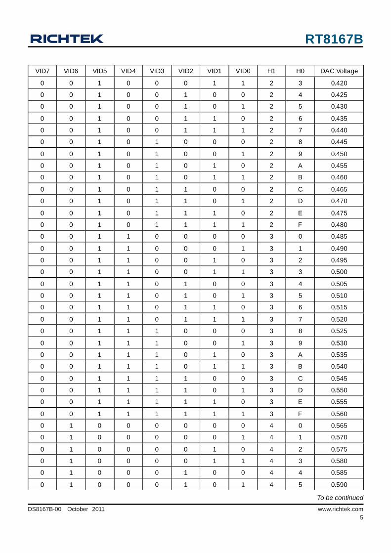
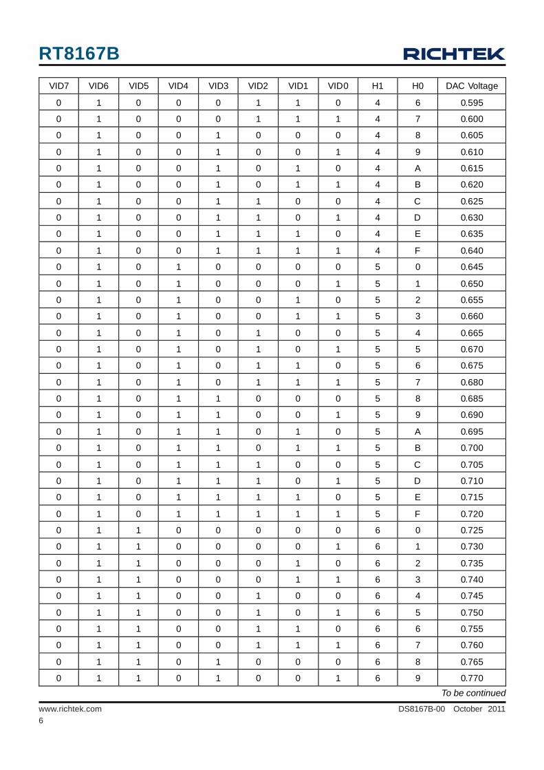
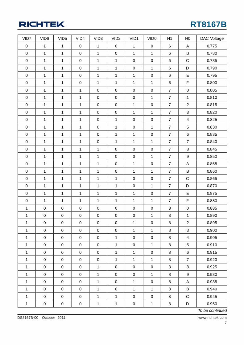
Table 1. IMVP7/VR12 Compliant VID Table
To be continued
RT8167B
5DS8167B-00 October 2011 www.richtek.com
VID7 VID6 VID5 VID4 VID3 VID2 VID1 VID0 H1 H0 DAC Voltage
0 0 1 0 0 0 1 1 2 3 0.420
0 0 1 0 0 1 0 0 2 4 0.425
0 0 1 0 0 1 0 1 2 5 0.430
0 0 1 0 0 1 1 0 2 6 0.435
0 0 1 0 0 1 1 1 2 7 0.440
0 0 1 0 1 0 0 0 2 8 0.445
0 0 1 0 1 0 0 1 2 9 0.450
0 0 1 0 1 0 1 0 2 A 0.455
0 0 1 0 1 0 1 1 2 B 0.460
0 0 1 0 1 1 0 0 2 C 0.465
0 0 1 0 1 1 0 1 2 D 0.470
0 0 1 0 1 1 1 0 2 E 0.475
0 0 1 0 1 1 1 1 2 F 0.480
0 0 1 1 0 0 0 0 3 0 0.485
0 0 1 1 0 0 0 1 3 1 0.490
0 0 1 1 0 0 1 0 3 2 0.495
0 0 1 1 0 0 1 1 3 3 0.500
0 0 1 1 0 1 0 0 3 4 0.505
0 0 1 1 0 1 0 1 3 5 0.510
0 0 1 1 0 1 1 0 3 6 0.515
0 0 1 1 0 1 1 1 3 7 0.520
0 0 1 1 1 0 0 0 3 8 0.525
0 0 1 1 1 0 0 1 3 9 0.530
0 0 1 1 1 0 1 0 3 A 0.535
0 0 1 1 1 0 1 1 3 B 0.540
0 0 1 1 1 1 0 0 3 C 0.545
0 0 1 1 1 1 0 1 3 D 0.550
0 0 1 1 1 1 1 0 3 E 0.555
0 0 1 1 1 1 1 1 3 F 0.560
0 1 0 0 0 0 0 0 4 0 0.565
0 1 0 0 0 0 0 1 4 1 0.570
0 1 0 0 0 0 1 0 4 2 0.575
0 1 0 0 0 0 1 1 4 3 0.580
0 1 0 0 0 1 0 0 4 4 0.585
0 1 0 0 0 1 0 1 4 5 0.590
To be continued
RT8167B
6DS8167B-00 October 2011www.richtek.com
VID7 VID6 VID5 VID4 VID3 VID2 VID1 VID0 H1 H0 DAC Voltage
0 1 0 0 0 1 1 0 4 6 0.595
0 1 0 0 0 1 1 1 4 7 0.600
0 1 0 0 1 0 0 0 4 8 0.605
0 1 0 0 1 0 0 1 4 9 0.610
0 1 0 0 1 0 1 0 4 A 0.615
0 1 0 0 1 0 1 1 4 B 0.620
0 1 0 0 1 1 0 0 4 C 0.625
0 1 0 0 1 1 0 1 4 D 0.630
0 1 0 0 1 1 1 0 4 E 0.635
0 1 0 0 1 1 1 1 4 F 0.640
0 1 0 1 0 0 0 0 5 0 0.645
0 1 0 1 0 0 0 1 5 1 0.650
0 1 0 1 0 0 1 0 5 2 0.655
0 1 0 1 0 0 1 1 5 3 0.660
0 1 0 1 0 1 0 0 5 4 0.665
0 1 0 1 0 1 0 1 5 5 0.670
0 1 0 1 0 1 1 0 5 6 0.675
0 1 0 1 0 1 1 1 5 7 0.680
0 1 0 1 1 0 0 0 5 8 0.685
0 1 0 1 1 0 0 1 5 9 0.690
0 1 0 1 1 0 1 0 5 A 0.695
0 1 0 1 1 0 1 1 5 B 0.700
0 1 0 1 1 1 0 0 5 C 0.705
0 1 0 1 1 1 0 1 5 D 0.710
0 1 0 1 1 1 1 0 5 E 0.715
0 1 0 1 1 1 1 1 5 F 0.720
0 1 1 0 0 0 0 0 6 0 0.725
0 1 1 0 0 0 0 1 6 1 0.730
0 1 1 0 0 0 1 0 6 2 0.735
0 1 1 0 0 0 1 1 6 3 0.740
0 1 1 0 0 1 0 0 6 4 0.745
0 1 1 0 0 1 0 1 6 5 0.750
0 1 1 0 0 1 1 0 6 6 0.755
0 1 1 0 0 1 1 1 6 7 0.760
0 1 1 0 1 0 0 0 6 8 0.765
0 1 1 0 1 0 0 1 6 9 0.770
To be continued
RT8167B
7DS8167B-00 October 2011 www.richtek.com
VID7 VID6 VID5 VID4 VID3 VID2 VID1 VID0 H1 H0 DAC Voltage
0 1 1 0 1 0 1 0 6 A 0.775
0 1 1 0 1 0 1 1 6 B 0.780
0 1 1 0 1 1 0 0 6 C 0.785
0 1 1 0 1 1 0 1 6 D 0.790
0 1 1 0 1 1 1 0 6 E 0.795
0 1 1 0 1 1 1 1 6 F 0.800
0 1 1 1 0 0 0 0 7 0 0.805
0 1 1 1 0 0 0 1 7 1 0.810
0 1 1 1 0 0 1 0 7 2 0.815
0 1 1 1 0 0 1 1 7 3 0.820
0 1 1 1 0 1 0 0 7 4 0.825
0 1 1 1 0 1 0 1 7 5 0.830
0 1 1 1 0 1 1 0 7 6 0.835
0 1 1 1 0 1 1 1 7 7 0.840
0 1 1 1 1 0 0 0 7 8 0.845
0 1 1 1 1 0 0 1 7 9 0.850
0 1 1 1 1 0 1 0 7 A 0.855
0 1 1 1 1 0 1 1 7 B 0.860
0 1 1 1 1 1 0 0 7 C 0.865
0 1 1 1 1 1 0 1 7 D 0.870
0 1 1 1 1 1 1 0 7 E 0.875
0 1 1 1 1 1 1 1 7 F 0.880
1 0 0 0 0 0 0 0 8 0 0.885
1 0 0 0 0 0 0 1 8 1 0.890
1 0 0 0 0 0 1 0 8 2 0.895
1 0 0 0 0 0 1 1 8 3 0.900
1 0 0 0 0 1 0 0 8 4 0.905
1 0 0 0 0 1 0 1 8 5 0.910
1 0 0 0 0 1 1 0 8 6 0.915
1 0 0 0 0 1 1 1 8 7 0.920
1 0 0 0 1 0 0 0 8 8 0.925
1 0 0 0 1 0 0 1 8 9 0.930
1 0 0 0 1 0 1 0 8 A 0.935
1 0 0 0 1 0 1 1 8 B 0.940
1 0 0 0 1 1 0 0 8 C 0.945
1 0 0 0 1 1 0 1 8 D 0.950
To be continued
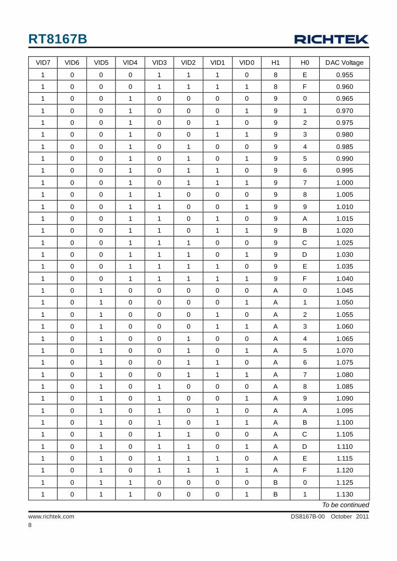
RT8167B
8DS8167B-00 October 2011www.richtek.com
To be continued
VID7 VID6 VID5 VID4 VID3 VID2 VID1 VID0 H1 H0 DAC Voltage
1 0 0 0 1 1 1 0 8 E 0.955
1 0 0 0 1 1 1 1 8 F 0.960
1 0 0 1 0 0 0 0 9 0 0.965
1 0 0 1 0 0 0 1 9 1 0.970
1 0 0 1 0 0 1 0 9 2 0.975
1 0 0 1 0 0 1 1 9 3 0.980
1 0 0 1 0 1 0 0 9 4 0.985
1 0 0 1 0 1 0 1 9 5 0.990
1 0 0 1 0 1 1 0 9 6 0.995
1 0 0 1 0 1 1 1 9 7 1.000
1 0 0 1 1 0 0 0 9 8 1.005
1 0 0 1 1 0 0 1 9 9 1.010
1 0 0 1 1 0 1 0 9 A 1.015
1 0 0 1 1 0 1 1 9 B 1.020
1 0 0 1 1 1 0 0 9 C 1.025
1 0 0 1 1 1 0 1 9 D 1.030
1 0 0 1 1 1 1 0 9 E 1.035
1 0 0 1 1 1 1 1 9 F 1.040
1 0 1 0 0 0 0 0 A 0 1.045
1 0 1 0 0 0 0 1 A 1 1.050
1 0 1 0 0 0 1 0 A 2 1.055
1 0 1 0 0 0 1 1 A 3 1.060
1 0 1 0 0 1 0 0 A 4 1.065
1 0 1 0 0 1 0 1 A 5 1.070
1 0 1 0 0 1 1 0 A 6 1.075
1 0 1 0 0 1 1 1 A 7 1.080
1 0 1 0 1 0 0 0 A 8 1.085
1 0 1 0 1 0 0 1 A 9 1.090
1 0 1 0 1 0 1 0 A A 1.095
1 0 1 0 1 0 1 1 A B 1.100
1 0 1 0 1 1 0 0 A C 1.105
1 0 1 0 1 1 0 1 A D 1.110
1 0 1 0 1 1 1 0 A E 1.115
1 0 1 0 1 1 1 1 A F 1.120
1 0 1 1 0 0 0 0 B 0 1.125
1 0 1 1 0 0 0 1 B 1 1.130
RT8167B
9DS8167B-00 October 2011 www.richtek.com
VID7 VID6 VID5 VID4 VID3 VID2 VID1 VID0 H1 H0 DAC Voltage
1 0 1 1 0 0 1 0 B 2 1.135
1 0 1 1 0 0 1 1 B 3 1.140
1 0 1 1 0 1 0 0 B 4 1.145
1 0 1 1 0 1 0 1 B 5 1.150
1 0 1 1 0 1 1 0 B 6 1.155
1 0 1 1 0 1 1 1 B 7 1.160
1 0 1 1 1 0 0 0 B 8 1.165
1 0 1 1 1 0 0 1 B 9 1.170
1 0 1 1 1 0 1 0 B A 1.175
1 0 1 1 1 0 1 1 B B 1.180
1 0 1 1 1 1 0 0 B C 1.185
1 0 1 1 1 1 0 1 B D 1.190
1 0 1 1 1 1 1 0 B E 1.195
1 0 1 1 1 1 1 1 B F 1.200
1 1 0 0 0 0 0 0 C 0 1.205
1 1 0 0 0 0 0 1 C 1 1.210
1 1 0 0 0 0 1 0 C 2 1.215
1 1 0 0 0 0 1 1 C 3 1.220
1 1 0 0 0 1 0 0 C 4 1.225
1 1 0 0 0 1 0 1 C 5 1.230
1 1 0 0 0 1 1 0 C 6 1.235
1 1 0 0 0 1 1 1 C 7 1.240
1 1 0 0 1 0 0 0 C 8 1.245
1 1 0 0 1 0 0 1 C 9 1.250
1 1 0 0 1 0 1 0 C A 1.255
1 1 0 0 1 0 1 1 C B 1.260
1 1 0 0 1 1 0 0 C C 1.265
1 1 0 0 1 1 0 1 C D 1.270
1 1 0 0 1 1 1 0 C E 1.275
1 1 0 0 1 1 1 1 C F 1.280
1 1 0 1 0 0 0 0 D 0 1.285
1 1 0 1 0 0 0 1 D 1 1.290
1 1 0 1 0 0 1 0 D 2 1.295
1 1 0 1 0 0 1 1 D 3 1.300
1 1 0 1 0 1 0 0 D 4 1.305
1 1 0 1 0 1 0 1 D 5 1.310
To be continued
RT8167B
10DS8167B-00 October 2011www.richtek.com
VID7 VID6 VID5 VID4 VID3 VID2 VID1 VID0 H1 H0 DAC Voltage
1 1 0 1 0 1 1 0 D 6 1.315
1 1 0 1 0 1 1 1 D 7 1.320
1 1 0 1 1 0 0 0 D 8 1.325
1 1 0 1 1 0 0 1 D 9 1.330
1 1 0 1 1 0 1 0 D A 1.335
1 1 0 1 1 0 1 1 D B 1.340
1 1 0 1 1 1 0 0 D C 1.345
1 1 0 1 1 1 0 1 D D 1.350
1 1 0 1 1 1 1 0 D E 1.355
1 1 0 1 1 1 1 1 D F 1.360
1 1 1 0 0 0 0 0 E 0 1.365
1 1 1 0 0 0 0 1 E 1 1.370
1 1 1 0 0 0 1 0 E 2 1.375
1 1 1 0 0 0 1 1 E 3 1.380
1 1 1 0 0 1 0 0 E 4 1.385
1 1 1 0 0 1 0 1 E 5 1.390
1 1 1 0 0 1 1 0 E 6 1.395
1 1 1 0 0 1 1 1 E 7 1.400
1 1 1 0 1 0 0 0 E 8 1.405
1 1 1 0 1 0 0 1 E 9 1.410
1 1 1 0 1 0 1 0 E A 1.415
1 1 1 0 1 0 1 1 E B 1.420
1 1 1 0 1 1 0 0 E C 1.425
1 1 1 0 1 1 0 1 E D 1.430
1 1 1 0 1 1 1 0 E E 1.435
1 1 1 0 1 1 1 1 E F 1.440
1 1 1 1 0 0 0 0 F 0 1.445
1 1 1 1 0 0 0 1 F 1 1.450
1 1 1 1 0 0 1 0 F 2 1.455
1 1 1 1 0 0 1 1 F 3 1.460
1 1 1 1 0 1 0 0 F 4 1.465
1 1 1 1 0 1 0 1 F 5 1.470
1 1 1 1 0 1 1 0 F 6 1.475
1 1 1 1 0 1 1 1 F 7 1.480
1 1 1 1 1 0 0 0 F 8 1.485
To be continued
RT8167B
11DS8167B-00 October 2011 www.richtek.com
VID7 VID6 VID5 VID4 VID3 VID2 VID1 VID0 H1 H0 DAC Voltage
1 1 1 1 1 0 0 1 F 9 1.490
1 1 1 1 1 0 1 0 F A 1.495
1 1 1 1 1 0 1 1 F B 1.500
1 1 1 1 1 1 0 0 F C 1.505
1 1 1 1 1 1 0 1 F D 1.510
1 1 1 1 1 1 1 0 F E 1.515
1 1 1 1 1 1 1 1 F F 1.520
RT8167B
12DS8167B-00 October 2011www.richtek.com
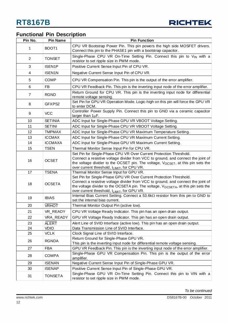
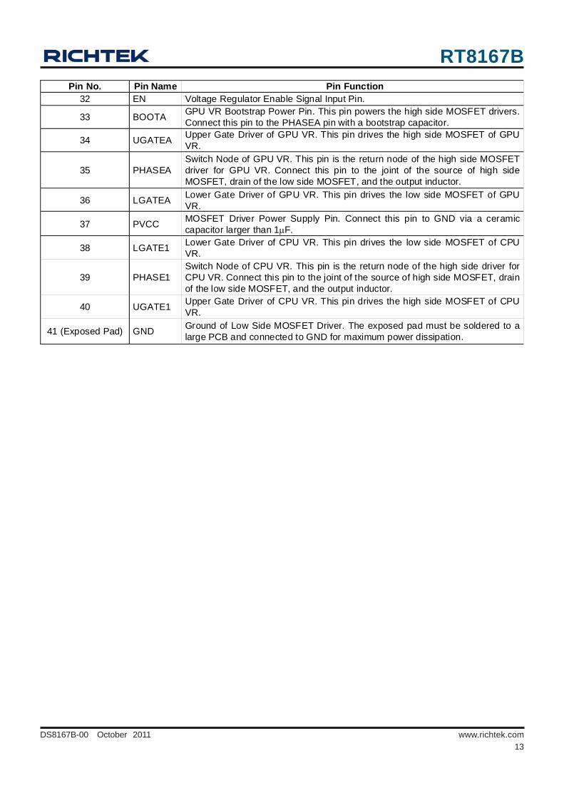
Functional Pin DescriptionPin No. Pin Name Pin Function
1 BOOT1 CPU VR Bootstrap Power Pin. This pin powers the high side MOSFET drivers. Connect this pin to the PHASE1 pin with a bootstrap capacitor.
2 TONSET Single-Phase CPU VR On-Time Setting Pin. Connect this pin to VIN with a resistor to set ripple size in PWM mode.
3 ISEN1P Positive Current Sense Input Pin of CPU VR.
4 ISEN1N Negative Current Sense Input Pin of CPU VR.
5 COMP CPU VR Compensation Pin. This pin is the output of the error amplifier.
6 FB CPU VR Feedback Pin. This pin is the inverting input node of the error amplifier.
7 RGND Return Ground for CPU VR. This pin is the inverting input node for differential remote voltage sensing.
8 GFXPS2 Set Pin for GPU VR Operation Mode. Logic-high on this pin will force the GPU VR to enter DCM.
9 VCC Controller Power Supply Pin. Connect this pin to GND via a ceramic capacitor larger than 1μF.
10 SETINIA ADC Input for Single-Phase GPU VR VBOOT Voltage Setting. 11 SETINI ADC Input for Single-Phase CPU VR VBOOT Voltage Setting. 12 TMPMAX ADC Input for Single-Phase CPU VR Maximum Temperature Setting. 13 ICCMAX ADC Input for Single-Phase CPU VR Maximum Current Setting. 14 ICCMAXA ADC Input for Single-Phase GPU VR Maximum Current Setting. 15 TSEN Thermal Monitor Sense Input Pin for CPU VR.
16 OCSET
Set Pin for Single-Phase CPU VR Over Current Protection Threshold. Connect a resistive voltage divider from VCC to ground, and connect the joint of the voltage divider to the OCSET pin. The voltage, VOCSET, at this pin sets the over current threshold, ILIMIT, for CPU VR.
17 TSENA Thermal Monitor Sense Input for GPU VR.
18 OCSETA
Set Pin for Single-Phase GPU VR Over Current Protection Threshold. Connect a resistive voltage divider from VCC to ground, and connect the joint of the voltage divider to the OCSETA pin. The voltage, VOCSETA, at this pin sets the over current threshold, ILIMIT, for GPU VR.
19 IBIAS Internal Bias Current Setting. Connect a 53.6kΩ resistor from this pin to GND to set the internal bias current.
20 VRHOT Thermal Monitor Output Pin (active low). 21 VR_READY CPU VR Voltage Ready Indicator. This pin has an open drain output. 22 VRA_READY GPU VR Voltage Ready Indicator. This pin has an open drain output. 23 ALERT Alert Line of SVID Interface (active low). This pin has an open drain output. 24 VDIO Data Transmission Line of SVID Interface. 25 VCLK Clock Signal Line of SVID Interface.
26 RGNDA Return Ground for Single-Phase GPU VR. This pin is the inverting input node for differential remote voltage sensing.
27 FBA GPU VR Feedback Pin. This pin is the inverting input node of the error amplifier.
28 COMPA Single-Phase GPU VR Compensation Pin. This pin is the output of the error amplifier.
29 ISENAN Negative Current Sense Input Pin of Single-Phase GPU VR. 30 ISENAP Positive Current Sense Input Pin of Single-Phase GPU VR.
31 TONSETA Single-Phase GPU VR On-Time Setting Pin. Connect this pin to VIN with a resistor to set ripple size in PWM mode.
To be continued
RT8167B
13DS8167B-00 October 2011 www.richtek.com
Pin No. Pin Name Pin Function 32 EN Voltage Regulator Enable Signal Input Pin.
33 BOOTA GPU VR Bootstrap Power Pin. This pin powers the high side MOSFET drivers. Connect this pin to the PHASEA pin with a bootstrap capacitor.
34 UGATEA Upper Gate Driver of GPU VR. This pin drives the high side MOSFET of GPU VR.
35 PHASEA Switch Node of GPU VR. This pin is the return node of the high side MOSFET driver for GPU VR. Connect this pin to the joint of the source of high side MOSFET, drain of the low side MOSFET, and the output inductor.
36 LGATEA Lower Gate Driver of GPU VR. This pin drives the low side MOSFET of GPU VR.
37 PVCC MOSFET Driver Power Supply Pin. Connect this pin to GND via a ceramic capacitor larger than 1μF.
38 LGATE1 Lower Gate Driver of CPU VR. This pin drives the low side MOSFET of CPU VR.
39 PHASE1 Switch Node of CPU VR. This pin is the return node of the high side driver for CPU VR. Connect this pin to the joint of the source of high side MOSFET, drain of the low side MOSFET, and the output inductor.
40 UGATE1 Upper Gate Driver of CPU VR. This pin drives the high side MOSFET of CPU VR.
41 (Exposed Pad) GND Ground of Low Side MOSFET Driver. The exposed pad must be soldered to a large PCB and connected to GND for maximum power dissipation.
RT8167B
14DS8167B-00 October 2011www.richtek.com
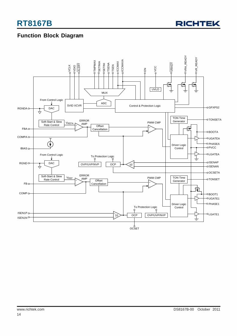
Function Block Diagram
ICC
MA
X
ICC
MA
XA
TSE
N
FBA
COMPA
ERROR AMP
TMPM
AX
Control & Protection Logic
MUX
ADCSVID XCVR
VD
IO
VC
LK
EN
VR
_RE
AD
Y
VR
A_R
EA
DY
RGNDA
PWM CMP
From Control Logic
VREFA
VC
C
UVLO
PVCC
BOOTA
UGATEA
PHASEA
LGATEA
SET
INIA
SET
INI
TSE
NA
TONSETATON Time Generator
Driver Logic Control
Offset Cancellation
GFXPS2
VR
HO
T
+
-
+
-
ALE
RT
DAC
+
-10OCPOVP/UVP/NVP
ERROR AMP
RGND
PWM CMP
From Control Logic
Soft-Start & Slew Rate Control
VREF
BOOT1UGATE1
PHASE1
LGATE1
TONSETTON Time Generator
Driver Logic Control
Offset Cancellation +
-
+
-
DAC
To Protection Logic
Soft-Start & Slew Rate Control
+
-10 OCP OVP/UVP/NVP
To Protection Logic
FB
COMP
ISEN1P
ISEN1N
OCSET
ISENAPISENAN
OCSETA
IBIAS
RT8167B
15DS8167B-00 October 2011 www.richtek.com
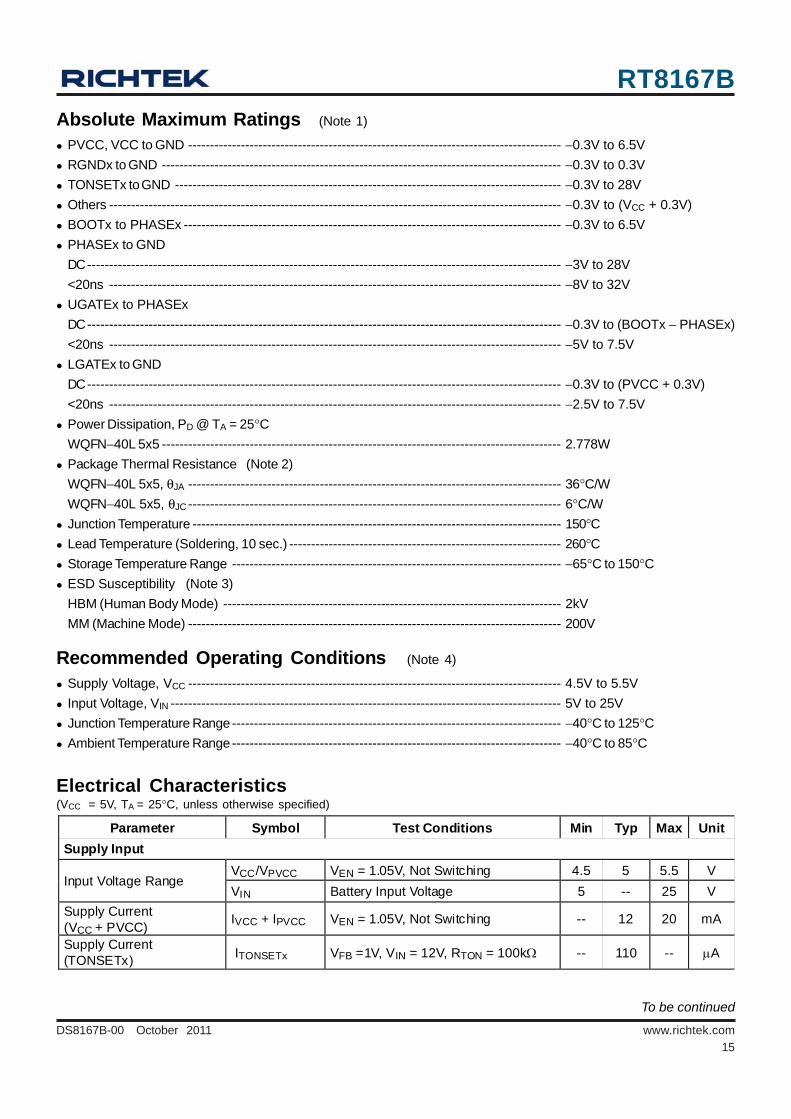
Recommended Operating Conditions (Note 4)
Supply Voltage, VCC ------------------------------------------------------------------------------------- 4.5V to 5.5VInput Voltage, VIN ----------------------------------------------------------------------------------------- 5V to 25VJunction Temperature Range--------------------------------------------------------------------------- −40°C to 125°CAmbient Temperature Range--------------------------------------------------------------------------- −40°C to 85°C
Absolute Maximum Ratings (Note 1)
PVCC, VCC to GND ------------------------------------------------------------------------------------- −0.3V to 6.5VRGNDx to GND ------------------------------------------------------------------------------------------- −0.3V to 0.3VTONSETx to GND ---------------------------------------------------------------------------------------- −0.3V to 28VOthers ------------------------------------------------------------------------------------------------------- −0.3V to (VCC + 0.3V)BOOTx to PHASEx -------------------------------------------------------------------------------------- −0.3V to 6.5VPHASEx to GNDDC------------------------------------------------------------------------------------------------------------ −3V to 28V<20ns ------------------------------------------------------------------------------------------------------- −8V to 32VUGATEx to PHASExDC------------------------------------------------------------------------------------------------------------ −0.3V to (BOOTx − PHASEx)<20ns ------------------------------------------------------------------------------------------------------- −5V to 7.5VLGATEx to GNDDC------------------------------------------------------------------------------------------------------------ −0.3V to (PVCC + 0.3V)<20ns ------------------------------------------------------------------------------------------------------- −2.5V to 7.5VPower Dissipation, PD @ TA = 25°CWQFN−40L 5x5 ------------------------------------------------------------------------------------------- 2.778WPackage Thermal Resistance (Note 2)WQFN−40L 5x5, θJA ------------------------------------------------------------------------------------- 36°C/WWQFN−40L 5x5, θJC ------------------------------------------------------------------------------------- 6°C/WJunction Temperature ------------------------------------------------------------------------------------ 150°CLead Temperature (Soldering, 10 sec.) -------------------------------------------------------------- 260°CStorage Temperature Range --------------------------------------------------------------------------- −65°C to 150°CESD Susceptibility (Note 3)HBM (Human Body Mode) ----------------------------------------------------------------------------- 2kVMM (Machine Mode) ------------------------------------------------------------------------------------- 200V
Electrical Characteristics(VCC = 5V, TA = 25°C, unless otherwise specified)
Parameter Symbol Test Conditions Min Typ Max Unit Supply Input
VCC/VPVCC VEN = 1.05V, Not Switching 4.5 5 5.5 V Input Voltage Range
VIN Battery Input Voltage 5 -- 25 V Supply Current (VCC + PVCC) IVCC + IPVCC VEN = 1.05V, Not Switching -- 12 20 mA
Supply Current (TONSETx) ITONSETx VFB =1V, VIN = 12V, RTON = 100kΩ -- 110 -- μA
To be continued
RT8167B
16DS8167B-00 October 2011www.richtek.com
To be continued
Parameter Symbol Test Conditions Min Typ Max Unit Shutdown Current (PVCC + VCC)
IVCC_SHDN + IPVCC_SHDN VEN = 0V -- -- 5 μA
Shutdown Current (TONSETx) ITONSETx_SHDN VEN = 0V -- -- 5 μA
TON Setting TONSETx Voltage VTONSETx IRTON = 80μA, VFBx = 1V 0.95 1.075 1.2 0V On-Time tON IRTON = 80μA, VFBx = 1V 315 350 385 ns TONSETx Input Current Range IRTON VFBx = 1.1V 25 -- 280 μA
Minimum Off-Time TOFF_MIN -- 350 -- ns GFX VR Forced DEM GFXPS2x Enable Threshold VGFXPS 4.3 -- -- V
GFXPS2x Disable Threshold VGFXPS -- -- 0.7 V
References and System Output Voltage VIDSVID Setting = 1.000V~1.520V OFSSVID Setting = 0V −0.5 0 0.5 %VID
VIDSVID Setting = 0.800V~1.000V OFSSVID Setting = 0V −5 0 5
VIDSVID Setting = 0.500V~0.800V OFSSVID Setting = 0V −8 0 8
VIDSVID Setting = 0.250V~0.500V OFSSVID Setting = 0V −8 0 8
DAC Accuracy (PS0/PS1) VFBx
VIDSVID Setting = 1.100V OFSSVID Setting = −0.640V~0.635V −10 0 10
mV
VINI_CORE = 0V, VINI_GFX = 0V 0 0.3125 0.5125
VINI_CORE = 0.9V, VINI_GFX = 0.9V 0.7375 0.9375 1.1375 VINI_CORE = 1V, VINI_GFX = 1V 1.3625 1.5625 1.7625
SETINIx Voltage VSETINIx
VINI_CORE = 1.1V, VINI_GFX = 1.1V 2.6125 -- 5
V
IBIAS Pin Voltage VIBIAS RIBIAS = 53.6kΩ 2.09 2.14 2.19 V SetVID Slow 2.5 3.125 3.75 Dynamic VID Slew
Rate SRDVID SetVID Fast 10 12.5 15
mV/μs
Error Amplifier DC Gain ADC RL = 47kΩ (Note5) 70 80 -- dB Gain-Bandwidth Product GBW CLOAD = 5pF (Note5) -- 10 -- MHz
Slew Rate SRCOMP CLOAD = 10pF (Gain = −4, RLOAD_COMP = 47kΩ, VCOMPx = 0.5V to 3V)
-- 5 -- V/μs
Output Voltage Range VCOMP RL = 47kΩ 0.5 -- 3.6 V
MAX Source/Sink Current ICOMP VCOMP = 2V -- 250 -- μA
Impedance of FBx RFBx 1 -- -- MΩ
RT8167B
17DS8167B-00 October 2011 www.richtek.com
To be continued
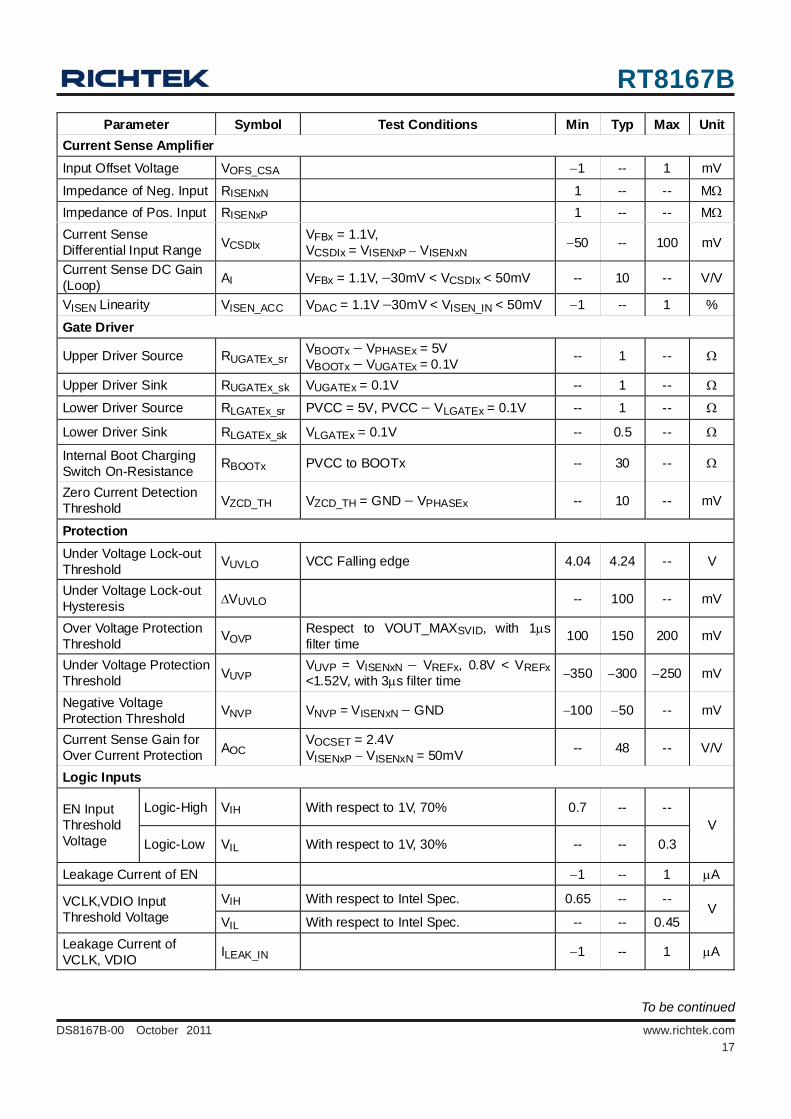
Parameter Symbol Test Conditions Min Typ Max Unit Current Sense Amplifier Input Offset Voltage VOFS_CSA −1 -- 1 mV
Impedance of Neg. Input RISENxN 1 -- -- MΩ Impedance of Pos. Input RISENxP 1 -- -- MΩ Current Sense Differential Input Range VCSDIx VFBx = 1.1V,
VCSDIx = VISENxP − VISENxN −50 -- 100 mV
Current Sense DC Gain (Loop) AI VFBx = 1.1V, −30mV < VCSDIx < 50mV -- 10 -- V/V
VISEN Linearity VISEN_ACC VDAC = 1.1V −30mV < VISEN_IN < 50mV −1 -- 1 %
Gate Driver
Upper Driver Source RUGATEx_sr VBOOTx − VPHASEx = 5V VBOOTx − VUGATEx = 0.1V -- 1 -- Ω
Upper Driver Sink RUGATEx_sk VUGATEx = 0.1V -- 1 -- Ω
Lower Driver Source RLGATEx_sr PVCC = 5V, PVCC − VLGATEx = 0.1V -- 1 -- Ω
Lower Driver Sink RLGATEx_sk VLGATEx = 0.1V -- 0.5 -- Ω
Internal Boot Charging Switch On-Resistance RBOOTx PVCC to BOOTx -- 30 -- Ω
Zero Current Detection Threshold VZCD_TH VZCD_TH = GND − VPHASEx -- 10 -- mV
Protection
Under Voltage Lock-out Threshold VUVLO VCC Falling edge 4.04 4.24 -- V
Under Voltage Lock-out Hysteresis ΔVUVLO -- 100 -- mV
Over Voltage Protection Threshold VOVP Respect to VOUT_MAXSVID, with 1μs
filter time 100 150 200 mV
Under Voltage Protection Threshold VUVP VUVP = VISENxN − VREFx, 0.8V < VREFx
<1.52V, with 3μs filter time −350 −300 −250 mV
Negative Voltage Protection Threshold VNVP VNVP = VISENxN − GND −100 −50 -- mV
Current Sense Gain for Over Current Protection AOC VOCSET = 2.4V
VISENxP − VISENxN = 50mV -- 48 -- V/V
Logic Inputs
Logic-High VIH With respect to 1V, 70% 0.7 -- -- EN Input Threshold Voltage Logic-Low VIL With respect to 1V, 30% -- -- 0.3
V
Leakage Current of EN −1 -- 1 μA
VIH With respect to Intel Spec. 0.65 -- -- VCLK,VDIO Input Threshold Voltage VIL With respect to Intel Spec. -- -- 0.45
V
Leakage Current of VCLK, VDIO ILEAK_IN −1 -- 1 μA
RT8167B
18DS8167B-00 October 2011www.richtek.com
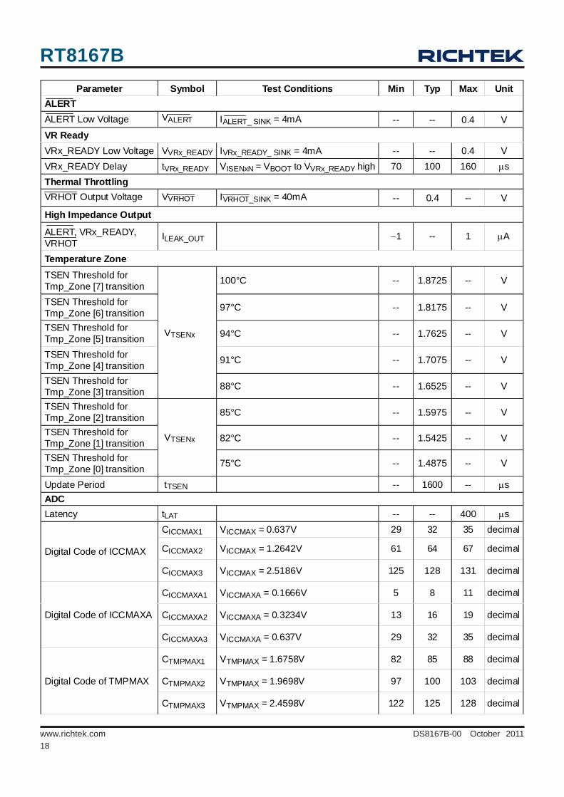
Parameter Symbol Test Conditions Min Typ Max Unit ALERT ALERT Low Voltage VALERT IALERT_ SINK = 4mA -- -- 0.4 V VR Ready VRx_READY Low Voltage VVRx_READY IVRx_READY_ SINK = 4mA -- -- 0.4 V VRx_READY Delay tVRx_READY VISENxN = VBOOT to VVRx_READY high 70 100 160 μs Thermal Throttling VRHOT Output Voltage VVRHOT IVRHOT_SINK = 40mA -- 0.4 -- V
High Impedance Output
ALERT, VRx_READY, VRHOT
ILEAK_OUT −1 -- 1 μA
Temperature Zone TSEN Threshold for Tmp_Zone [7] transition 100°C -- 1.8725 -- V
TSEN Threshold for Tmp_Zone [6] transition 97°C -- 1.8175 -- V
TSEN Threshold for Tmp_Zone [5] transition 94°C -- 1.7625 -- V
TSEN Threshold for Tmp_Zone [4] transition 91°C -- 1.7075 -- V
TSEN Threshold for Tmp_Zone [3] transition
VTSENx
88°C -- 1.6525 -- V
TSEN Threshold for Tmp_Zone [2] transition 85°C -- 1.5975 -- V
TSEN Threshold for Tmp_Zone [1] transition 82°C -- 1.5425 -- V
TSEN Threshold for Tmp_Zone [0] transition
VTSENx
75°C -- 1.4875 -- V
Update Period tTSEN -- 1600 -- μs ADC Latency tLAT -- -- 400 μs
CICCMAX1 VICCMAX = 0.637V 29 32 35 decimal
CICCMAX2 VICCMAX = 1.2642V 61 64 67 decimal Digital Code of ICCMAX
CICCMAX3 VICCMAX = 2.5186V 125 128 131 decimal
CICCMAXA1 VICCMAXA = 0.1666V 5 8 11 decimal
CICCMAXA2 VICCMAXA = 0.3234V 13 16 19 decimal Digital Code of ICCMAXA
CICCMAXA3 VICCMAXA = 0.637V 29 32 35 decimal
CTMPMAX1 VTMPMAX = 1.6758V 82 85 88 decimal
CTMPMAX2 VTMPMAX = 1.9698V 97 100 103 decimal Digital Code of TMPMAX
CTMPMAX3 VTMPMAX = 2.4598V 122 125 128 decimal
RT8167B
19DS8167B-00 October 2011 www.richtek.com
Note 1. Stresses listed as the above “Absolute Maximum Ratings” may cause permanent damage to the device. These are for
stress ratings. Functional operation of the device at these or any other conditions beyond those indicated in the
operational sections of the specifications is not implied. Exposure to absolute maximum rating conditions for extended
periods may remain possibility to affect device reliability.
Note 2. θJA is measured in the natural convection at TA = 25°C on a high effective thermal conductivity four-layer test board of
JEDEC 51-7 thermal measurement standard. The measurement case position of θJC is on the exposed pad of the
package.
Note 3. Devices are ESD sensitive. Handling precaution is recommended.
Note 4. The device is not guaranteed to function outside its operating conditions.
Note 5. Guaranteed by design.
RT8167B
20DS8167B-00 October 2011www.richtek.com
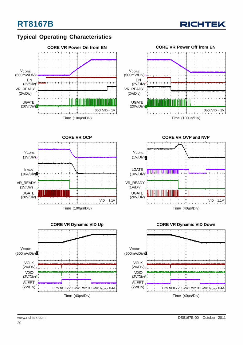
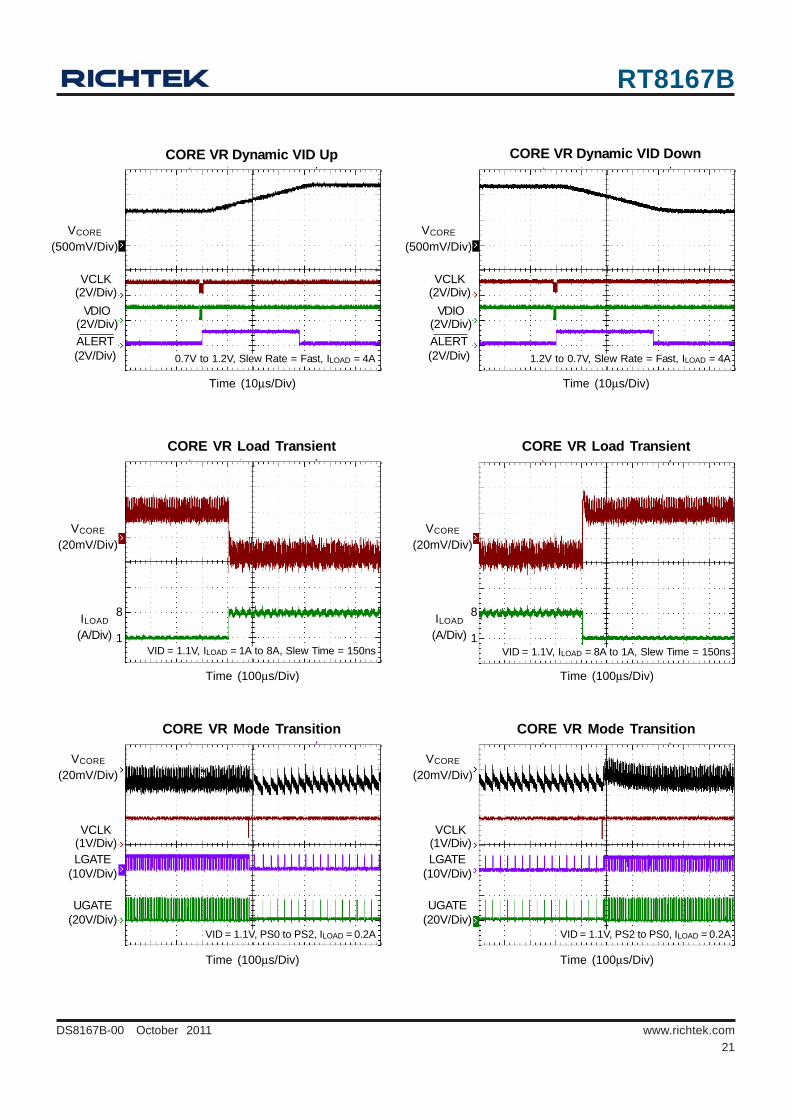
Typical Operating Characteristics
Boot VID = 1V
Time (100μs/Div)
CORE VR Power On from EN
EN(2V/Div)
VCORE(500mV/Div)
VR_READY(2V/Div)
UGATE(20V/Div)
Time (100μs/Div)
CORE VR Power Off from EN
Boot VID = 1V
EN(2V/Div)
VCORE(500mV/Div)
VR_READY(2V/Div)
UGATE(20V/Div)
VID = 1.1V
Time (100μs/Div)
CORE VR OCP
ILOAD(10A/Div)
VCORE
(1V/Div)
VR_READY(1V/Div)
UGATE(20V/Div)
Time (40μs/Div)
CORE VR OVP and NVP
VID = 1.1V
LGATE(10V/Div)
VCORE
(1V/Div)
VR_READY(1V/Div)
UGATE(20V/Div)
0.7V to 1.2V, Slew Rate = Slow, ILOAD = 4A
Time (40μs/Div)
CORE VR Dynamic VID Up
VDIO(2V/Div)
VCLK(2V/Div)
VCORE
(500mV/Div)
ALERT(2V/Div)
Time (40μs/Div)
CORE VR Dynamic VID Down
1.2V to 0.7V, Slew Rate = Slow, ILOAD = 4AALERT(2V/Div)
VCORE
(500mV/Div)
VDIO(2V/Div)
VCLK(2V/Div)
RT8167B
21DS8167B-00 October 2011 www.richtek.com
Time (10μs/Div)
CORE VR Dynamic VID Up
0.7V to 1.2V, Slew Rate = Fast, ILOAD = 4A
VDIO(2V/Div)
VCLK(2V/Div)
VCORE
(500mV/Div)
ALERT(2V/Div)
Time (10μs/Div)
CORE VR Dynamic VID Down
1.2V to 0.7V, Slew Rate = Fast, ILOAD = 4A
VCORE
(500mV/Div)
ALERT(2V/Div)
VDIO(2V/Div)
VCLK(2V/Div)
VID = 1.1V, ILOAD = 1A to 8A, Slew Time = 150ns
Time (100μs/Div)
CORE VR Load Transient
VCORE
(20mV/Div)
8
1ILOAD
(A/Div)
Time (100μs/Div)
CORE VR Load Transient
VID = 1.1V, ILOAD = 8A to 1A, Slew Time = 150ns
VCORE
(20mV/Div)
8
1ILOAD
(A/Div)
VID = 1.1V, PS0 to PS2, ILOAD = 0.2A
Time (100μs/Div)
CORE VR Mode Transition
UGATE(20V/Div)
VCLK(1V/Div)LGATE
(10V/Div)
VCORE
(20mV/Div)
Time (100μs/Div)
CORE VR Mode Transition
VID = 1.1V, PS2 to PS0, ILOAD = 0.2A
UGATE(20V/Div)
VCORE
(20mV/Div)
VCLK(1V/Div)LGATE
(10V/Div)
RT8167B
22DS8167B-00 October 2011www.richtek.com
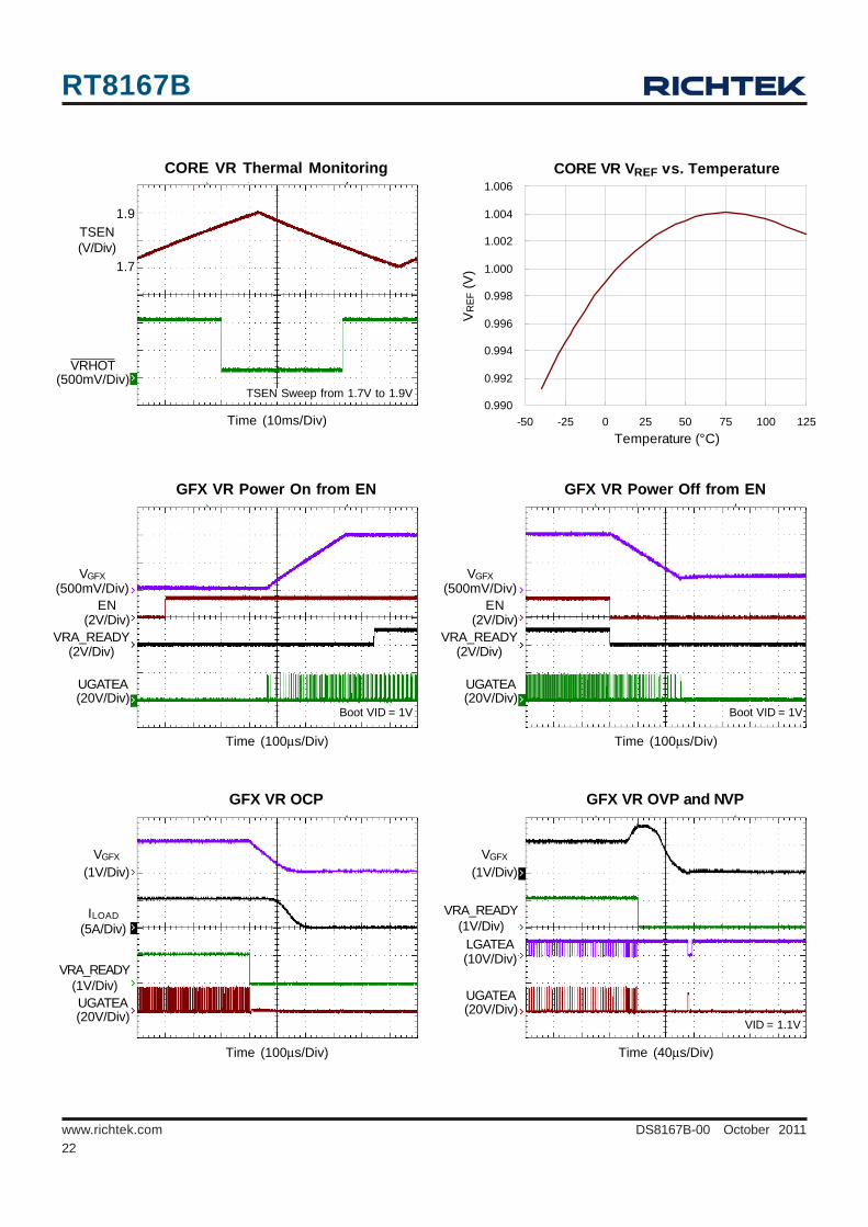
CORE VR VREF vs. Temperature
0.990
0.992
0.994
0.996
0.998
1.000
1.002
1.004
1.006
-50 -25 0 25 50 75 100 125Temperature (°C)
VR
EF (V
)
Time (100μs/Div)
GFX VR OCP
ILOAD(5A/Div)
VGFX
(1V/Div)
VRA_READY(1V/Div)UGATEA(20V/Div)
Time (40μs/Div)
GFX VR OVP and NVP
VID = 1.1V
LGATEA(10V/Div)
VGFX
(1V/Div)
VRA_READY(1V/Div)
UGATEA(20V/Div)
Time (100μs/Div)
GFX VR Power On from EN
Boot VID = 1V
EN(2V/Div)
VGFX(500mV/Div)
VRA_READY(2V/Div)
UGATEA(20V/Div)
Time (100μs/Div)
GFX VR Power Off from EN
Boot VID = 1V
UGATEA(20V/Div)
EN(2V/Div)
VGFX(500mV/Div)
VRA_READY(2V/Div)
TSEN Sweep from 1.7V to 1.9V
Time (10ms/Div)
CORE VR Thermal Monitoring
VRHOT(500mV/Div)
TSEN(V/Div)
1.9
1.7
RT8167B
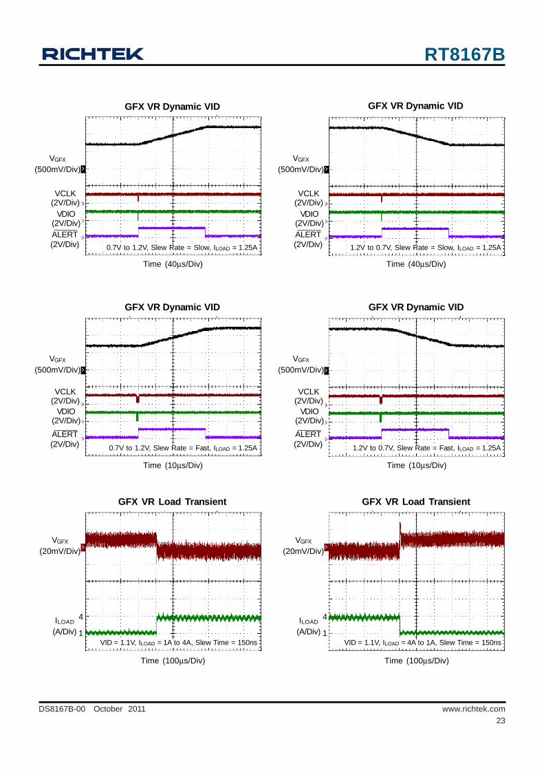
23DS8167B-00 October 2011 www.richtek.com
Time (40μs/Div)
GFX VR Dynamic VID
0.7V to 1.2V, Slew Rate = Slow, ILOAD = 1.25A
VDIO(2V/Div)
VCLK(2V/Div)
VGFX
(500mV/Div)
ALERT(2V/Div)
Time (40μs/Div)
GFX VR Dynamic VID
ALERT(2V/Div)
VGFX
(500mV/Div)
1.2V to 0.7V, Slew Rate = Slow, ILOAD = 1.25A
VDIO(2V/Div)
VCLK(2V/Div)
Time (10μs/Div)
GFX VR Dynamic VID
0.7V to 1.2V, Slew Rate = Fast, ILOAD = 1.25A
VDIO(2V/Div)
VCLK(2V/Div)
VGFX
(500mV/Div)
ALERT(2V/Div)
Time (10μs/Div)
GFX VR Dynamic VID
ALERT(2V/Div) 1.2V to 0.7V, Slew Rate = Fast, ILOAD = 1.25A
VDIO(2V/Div)
VCLK(2V/Div)
VGFX
(500mV/Div)
Time (100μs/Div)
GFX VR Load Transient
VID = 1.1V, ILOAD = 1A to 4A, Slew Time = 150ns
VGFX
(20mV/Div)
4
1ILOAD
(A/Div)
Time (100μs/Div)
GFX VR Load Transient
VID = 1.1V, ILOAD = 4A to 1A, Slew Time = 150ns
VGFX
(20mV/Div)
4
1ILOAD
(A/Div)
RT8167B
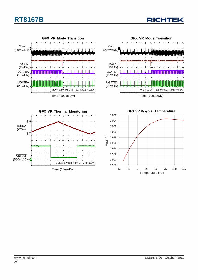
24DS8167B-00 October 2011www.richtek.com
GFX VR VREF vs. Temperature
0.988
0.990
0.992
0.994
0.996
0.998
1.000
1.002
1.004
1.006
-50 -25 0 25 50 75 100 125Temperature (°C)
VR
EF (V
)
Time (100μs/Div)
GFX VR Mode Transition
VID = 1.1V, PS2 to PS0, ILOAD = 0.1A
UGATEA(20V/Div)
VGFX
(20mV/Div)
VCLK(1V/Div)
LGATEA(10V/Div)
Time (100μs/Div)
GFX VR Mode Transition
VID = 1.1V, PS0 to PS2, ILOAD = 0.1A
UGATEA(20V/Div)
VCLK(1V/Div)
LGATEA(10V/Div)
VGFX
(20mV/Div)
Time (10ms/Div)
GFX VR Thermal Monitoring
TSENA Sweep from 1.7V to 1.9V
1.9
1.7
TSENA(V/Div)
VRHOT(500mV/Div)
RT8167B
25DS8167B-00 October 2011 www.richtek.com
Application InformationThe RT8167B is a VR12/IMVP7 compliant, dual single-phase synchronous Buck PWM controller for the CPUCORE VR and GFX VR. The gate drivers are embeddedto facilitate PCB design and reduce the total BOM cost. Aserial VID (SVID) interface is built-in in the RT8167B tocommunicate with Intel VR12/IMVP7 compliant CPU.
The RT8167B adopts G-NAVPTM (Green Native AVP),which is Richtek's proprietary topology derived from finiteDC gain compensator, making it an easy setting PWMcontroller to meet AVP requirements. The load line canbe easily programmed by setting the DC gain of the erroramplifier. The RT8167B has fast transient response dueto the G-NAVPTM commanding variable switchingfrequency.
G-NAVPTM topology also represents a high efficiencysystem with green power concept. With G-NAVPTM
topology, the RT8167B becomes a green power controllerwith high efficiency under heavy load, light load, and verylight load conditions. The RT8167B supports modetransition function between CCM and DEM. These differentoperating states allow the overall power system to havelow power loss. By utilizing the G-NAVPTM topology, theoperating frequency of RT8167B varies with output voltage,load and VIN to further enhance the efficiency even in CCM.
The built-in high accuracy DAC converts the SVID coderanging from 0.25V to 1.52V with 5mV per step. Thedifferential remote output voltage sense and high accuracyDAC allow the system to have high output voltage accuracy.
The RT8167B supports VR12/IMVP7 compatible powermanagement states and VID on-the-fly function. The powermanagement states include DEM in PS2/PS3 and Forced-CCM in PS1/PS0. The VID on-the-fly function has threedifferent slew rates : Fast, Slow and Decay. The RT8167Bintegrates a high accuracy ADC for platform settingfunctions, such as no-load offset and over current level.The controller supports both DCR and sense-resistorcurrent sensing. The RT8167B provides VR ready outputsignals of both CORE VR and GFX VR. It also featurescomplete fault protection functions including over voltage,under voltage, negative voltage, over current and undervoltage lockout. The RT8167B is available in a WQFN-48L 6x6 small foot print package.
Design ToolTo help users reduce efforts and errors caused by manualcalculations, a user-friendly design tool is now availableon request. This design tool calculates all necessarydesign parameters by entering user's requirements.Please contact Richtek's representatives for details.
Serial VID (SVID) InterfaceSVID is a three-wire serial synchronous interface definedby Intel. The three wire bus includes VDIO, VCLK andALERT signals. The master (Intel's VR12/IMVP7 CPU)initiates and terminates SVID transactions and drives theVDIO, VCLK, and ALERT during a transaction. The slave(RT8167B) receives the SVID transactions and actsaccordingly.
RT8167B
26DS8167B-00 October 2011www.richtek.com
Standard Serial VID Command
Code Commands Master Payload Contents
Slave Payload Contents Description
00h not supported N/A N/A N/A
01h SetVID_Fast VID code N/A Set new target VID code, VR jumps to new VID target with controlled default “fast” slew rate 12.5mV/μs.
02h SetVID_Slow VID code N/A Set new target VID code, VR jumps to new VID target with controlled default “slow” slew rate 3.125mV/μs.
03h SetVID_Decay VID code N/A
Set new target VID code, VR jumps to new VID target, but does not control the slew rate. The output voltage decays at a rate proportional to the load current
04h SetPS Byte indicating power states N/A Set power state
05h SetRegADR Pointer of registers in data table N/A Set the pointer of the data register
06h SetReg DAT New data register content N/A Write the contents to the data register
07h GetReg Pointer of registers in data table
Specified Register Contents
Slave returns the contents of the specified register as the payload
08h -
1Fh not supported N/A N/A N/A
RT8167B
27DS8167B-00 October 2011 www.richtek.com
Data and Configuration RegisterIndex Register Name Description Access Default 00h Vendor ID Vendor ID, default 1Eh. RO, Vendor 1Eh 01h Product ID Product ID. RO, Vendor 65h 02h Product Revision Product Revision. RO, Vendor 01h 05h Protocol ID SVID Protocol ID. RO, Vendor 01h
06h VR_Capability Bit mapped register, identifies the SVID VR capabilities and which of the optional telemetry register are supported.
RO, Vendor 81h
10h Status_1 Data register containing the status of VR. R-M, W-PWM 00h 11h Status-2 Data register containing the status of transmission. R-M, W-PWM 00h
12h Temperature Zone
Data register showing temperature zone that have been entered. R-M, W-PWM 00h
15h Output_Current Data register showing direct ADC conversion of averaged output current. R-M, W-PWM 00h
1Ch Status_2_lastread The register contains a copy of the status_2. R-M, W-PWM 00h
21h ICC_Max Data register containing the maximum ICC of platform supports. Binary format in Amp, IE 64h = 100A.
RO, Platform --
22h Temp_Max
Data register containing the temperature max the platform supports. Binary format in °C, IE 64h = 100°C Only for CORE VR
RO, Platform --
24h SR-Fast Data register containing the capability of fast slew rate the platform can sustains. Binary format in mV/μs, IE 0Ah = 10mV/μs.
RO 0Ah
25h SR-Slow Data register containing the capability of slow slew rate. Binary format in mV/μs IE 02h = 2.5mV/μs. RO 02h
30h VOUT_Max The register is programmed by the master and sets the maximum VID. RW, Master BFh
31h VID Setting Data register containing currently programmed VID. RW, Master 00h
32h Power State Register containing the current programmed power state. RW, Master 00h
33h Offset Set offset in VID steps. RW, Master 00h
34h Multi VR Config Bit mapped data register which configures multiple VRs behavior on the same bus. RW, Master 00h
35h Pointer Scratch pad register for temporary storage of the SetRegADR pointer register. RW, Master 30h
Notes :RO = Read OnlyRW = Read/WriteR-M = Read by MasterW-PWM = Write by PWM onlyVendor = hard coded by VR vendorPlatform = programmed by platformMaster = programmed by the masterPWM = programmed by the VR control IC
RT8167B
28DS8167B-00 October 2011www.richtek.com
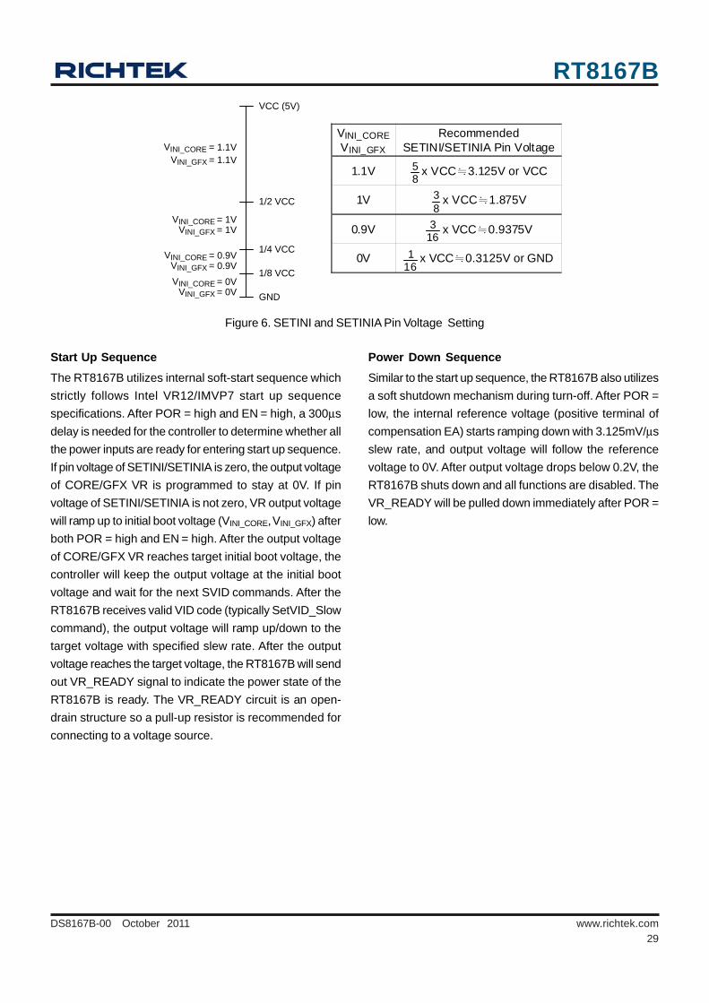
Figure 5. ADC Pins Setting
A/D Converter
ICCMAX
ICCMAXA
TMPMAX
VCC
ICCMAX, ICCMAXA and TMPMAXThe RT8167B provides ICCMAX, ICCMAXA and TMPMAXpins for platform users to set the maximum level of outputcurrent or VR temperature: ICCMAX for CORE VRmaximum current, ICCMAXA for GFX VR maximumcurrent, and TMPMAX for CORE VR maximumtemperature.
To set ICCMAX, ICCMAXA and TMPMAX, platformdesigners should use resistive voltage dividers on thesethree pins. The current of the divider should be severalmilli-Amps to avoid noise effect. The three items sharethe same algorithms : the ADC divides 5V into 255 levels.Therefore, LSB = 5/255 = 19.6mV, which means 19.6mVapplied to ICCMAX pin equals to 1A setting. For example,if a platform designer wants to set TMPMAX to 120°C, thevoltage applied to TMPMAX should be 120 x 19.6mV =2.352V. The ADC circuit inside these three pins willdecode the voltage applied and store the maximum current/temperature setting into ICC_MAX and Temp_Maxregisters. The ADC monitors and decodes the voltage atthese three pins only after EN = high. If EN = low, theRT8167B will not take any action even when the VR outputcurrent or temperature exceeds its maximum setting atthese ADC pins. The maximum level settings at theseADC pins are different from over current protection or overtemperature protection. That means, these maximum levelsetting pins are only for platform users to define theirsystem operating conditions and these messages will onlybe utilized by the CPU.
VINI_CORE and VINI_GFX SettingThe initial start up voltage (VINI_CORE, VINI_GFX) of theRT8167B can be set by platform users through SETINIand SETINIA pins. Voltage divider circuit is recommendedto be applied to SETINI and SETINIA pins. The VINI_CORE/VINI_GFX relate to SETINI/SETINIA pin voltage setting asshown in Figure 6. Recommended voltage setting at SETINIand SETINIA pins are also shown in Figure 6.
Precise Reference Current GenerationThe RT8167B includes extensive analog circuits insidethe controller. These analog circuits need very precisereference voltage/current to drive these analog devices.The RT8167B will auto-generate a 2.14V voltage sourceat IBIAS pin, and a 53.6kΩ resistor is required to beconnected between IBIAS and analog ground. Throughthis connection, the RT8167B generates a 40μA currentfrom IBIAS pin to analog ground and this 40μA current willbe mirrored inside the RT8167B for internal use. Othertypes of connection or other values of resistance appliedat the IBIAS pin may cause failure of the RT8167B's analogcircuits. Thus a 53.6kΩ resistor is the only recommendedcomponent to be connected to the IBIAS pin. Theresistance accuracy of this resistor is recommended tobe at least 1%.
Figure 4. IBIAS Setting
+
-
IBIAS
53.6k
Current Mirror
+-
2.14V
Power Ready Detection and Power On Reset (POR)During start-up, the RT8167B detects the voltage on thevoltage input pins : VCC and EN. When VCC > VUVLO,the RT8167B will recognize the power state of system tobe ready (POR = high) and wait for enable command atEN pin. After POR = high and EN > VENTH, the RT8167Bwill enter start-up sequence for both CORE VR and GFXVR. If the voltage on any voltage pin drops below PORthreshold (POR = low), the RT8167B will enter power downsequence and all the functions will be disabled. SVID willbe invalid within 300μs after chip becomes enabled. Allthe protection latches (OVP, OCP, UVP, OTP) will becleared only after POR = low. EN = low will not clearthese latches.
Figure 3. Power Ready Detection and Power On Reset(POR)
VUVLO
VENTH
+
-
+
-
POR
Chip EN
VCC
EN
RT8167B
29DS8167B-00 October 2011 www.richtek.com
Figure 6. SETINI and SETINIA Pin Voltage Setting
Start Up SequenceThe RT8167B utilizes internal soft-start sequence whichstrictly follows Intel VR12/IMVP7 start up sequencespecifications. After POR = high and EN = high, a 300μsdelay is needed for the controller to determine whether allthe power inputs are ready for entering start up sequence.If pin voltage of SETINI/SETINIA is zero, the output voltageof CORE/GFX VR is programmed to stay at 0V. If pinvoltage of SETINI/SETINIA is not zero, VR output voltagewill ramp up to initial boot voltage (VINI_CORE, VINI_GFX) afterboth POR = high and EN = high. After the output voltageof CORE/GFX VR reaches target initial boot voltage, thecontroller will keep the output voltage at the initial bootvoltage and wait for the next SVID commands. After theRT8167B receives valid VID code (typically SetVID_Slowcommand), the output voltage will ramp up/down to thetarget voltage with specified slew rate. After the outputvoltage reaches the target voltage, the RT8167B will sendout VR_READY signal to indicate the power state of theRT8167B is ready. The VR_READY circuit is an open-drain structure so a pull-up resistor is recommended forconnecting to a voltage source.
VINI_CORE VINI_GFX
Recommended SETINI/SETINIA Pin Voltage
1.1V 58
x VCC≒3.125V or VCC
1V 38
x VCC≒1.875V
0.9V 316
x VCC≒0.9375V
0V 116
x VCC≒0.3125V or GND
VCC (5V)
GND
1/8 VCC
1/4 VCC
1/2 VCC
VINI_CORE = 0.9VVINI_GFX = 0.9V
VINI_CORE = 1.1VVINI_GFX = 1.1V
VINI_CORE = 1VVINI_GFX = 1V
VINI_CORE = 0VVINI_GFX = 0V
Power Down SequenceSimilar to the start up sequence, the RT8167B also utilizesa soft shutdown mechanism during turn-off. After POR =low, the internal reference voltage (positive terminal ofcompensation EA) starts ramping down with 3.125mV/μsslew rate, and output voltage will follow the referencevoltage to 0V. After output voltage drops below 0.2V, theRT8167B shuts down and all functions are disabled. TheVR_READY will be pulled down immediately after POR =low.
RT8167B
30DS8167B-00 October 2011www.richtek.com
Figure 7 (a). Power sequence for RT8167B (VINI_CORE = VINI_GFX = 0V)
Figure 7 (b). Power sequence for RT8167B (VINI_CORE 0, VINI_GFX 0V)≠ ≠
EN
SVID Valid xxXX
VCORE
VR_READY100µs
POR
0.2VCORE VR
Operation Mode CCM CCM
0.2VVGFX
SVID defined
CCM SVID definedGFX VR
Operation Mode
100µsVRA_READY
CCM
300µs
Off
Off
VCC
EN Chip(Internal Signal)
Off
Off
VRA_READY
EN Chip(Internal Signal)
SVID Valid xxXX
VCORE
VR_READY100µs
POR
0.2VCORE VR
Operation Mode CCM CCMOff
0.2VVGFX
SVID defined
CCMOff SVID definedGFX VR
Operation Mode CCM
250µs
Off
Off
VCC
EN
100µs
300µs
VINI_GFX
VINI_CORE
50µs
RT8167B
31DS8167B-00 October 2011 www.richtek.com
Since the DCR of inductor is temperature dependent, itaffects the output accuracy in high temperature conditions.Temperature compensation is recommended for thelossless inductor DCR current sense method. Figure 10shows a simple but effective way of compensating thetemperature variations of the sense resistor using an NTCthermistor placed in the feedback path.
Figure 10. Loop Setting with Temperature Compensation
VCC_SENSE
-
+ VSS_SENSE
FBxRGNDx
COMPx
C2 C1
R2 R1b
EA
R1a
NTC
-+
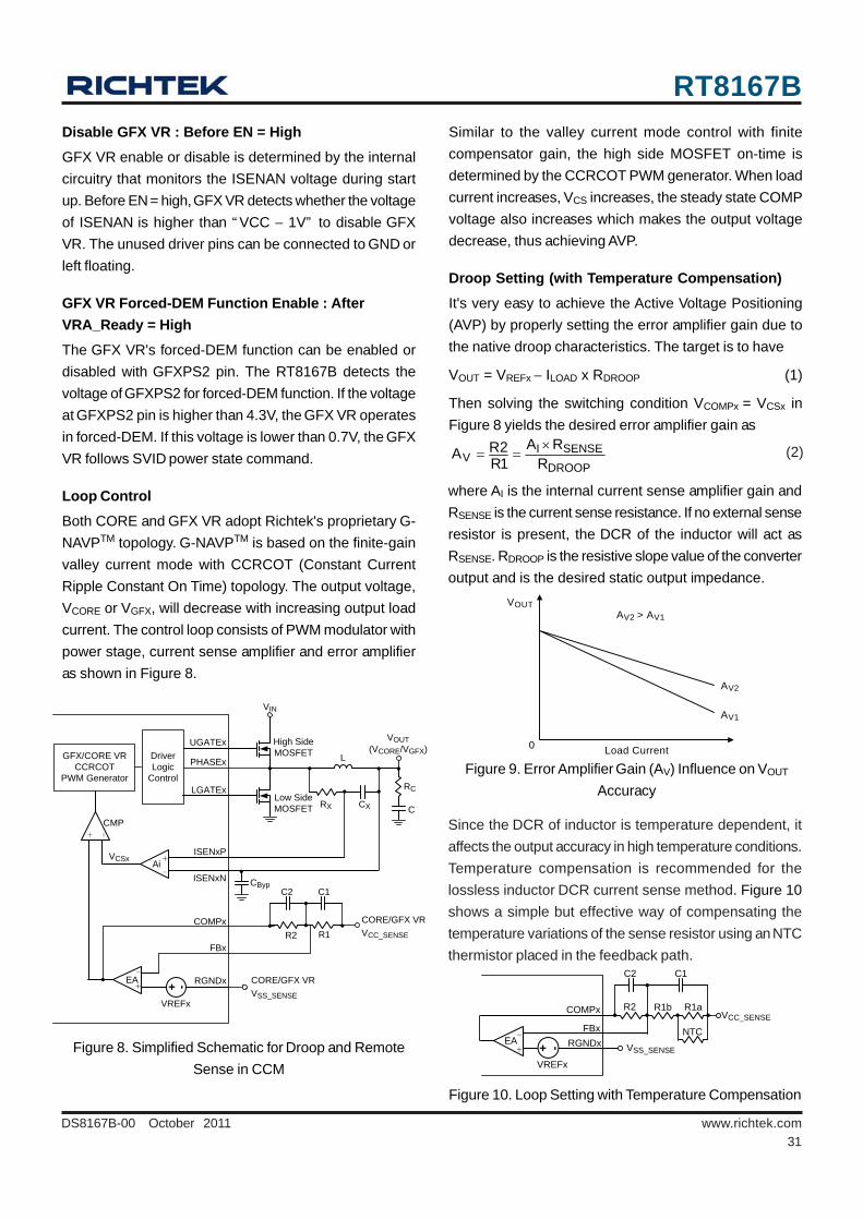
VREFxFigure 8. Simplified Schematic for Droop and Remote
Sense in CCM
Disable GFX VR : Before EN = HighGFX VR enable or disable is determined by the internalcircuitry that monitors the ISENAN voltage during startup. Before EN = high, GFX VR detects whether the voltageof ISENAN is higher than “VCC − 1V” to disable GFXVR. The unused driver pins can be connected to GND orleft floating.
GFX VR Forced-DEM Function Enable : AfterVRA_Ready = HighThe GFX VR's forced-DEM function can be enabled ordisabled with GFXPS2 pin. The RT8167B detects thevoltage of GFXPS2 for forced-DEM function. If the voltageat GFXPS2 pin is higher than 4.3V, the GFX VR operatesin forced-DEM. If this voltage is lower than 0.7V, the GFXVR follows SVID power state command.
Loop ControlBoth CORE and GFX VR adopt Richtek's proprietary G-NAVPTM topology. G-NAVPTM is based on the finite-gainvalley current mode with CCRCOT (Constant CurrentRipple Constant On Time) topology. The output voltage,VCORE or VGFX, will decrease with increasing output loadcurrent. The control loop consists of PWM modulator withpower stage, current sense amplifier and error amplifieras shown in Figure 8.
Similar to the valley current mode control with finitecompensator gain, the high side MOSFET on-time isdetermined by the CCRCOT PWM generator. When loadcurrent increases, VCS increases, the steady state COMPvoltage also increases which makes the output voltagedecrease, thus achieving AVP.
Droop Setting (with Temperature Compensation)It's very easy to achieve the Active Voltage Positioning(AVP) by properly setting the error amplifier gain due tothe native droop characteristics. The target is to have
VOUT = VREFx − ILOAD x RDROOP (1)
Then solving the switching condition VCOMPx = VCSx inFigure 8 yields the desired error amplifier gain as
where AI is the internal current sense amplifier gain andRSENSE is the current sense resistance. If no external senseresistor is present, the DCR of the inductor will act asRSENSE. RDROOP is the resistive slope value of the converteroutput and is the desired static output impedance.
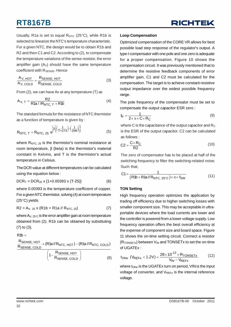
Figure 9. Error Amplifier Gain (AV) Influence on VOUT
Accuracy
AV1
AV2
AV2 > AV1
VOUT
Load Current0
×= = I SENSE
VDROOP
A RR2AR1 R
(2)
VIN
ISENxP
ISENxN
FBx
RGNDx
High Side MOSFET L
RX CX
RC
C
R1R2
CORE/GFX VR VCC_SENSE
COMPx
VCSx
C2 C1
VREFx
GFX/CORE VR CCRCOT
PWM Generator
Driver Logic
Control
CByp
UGATEx
PHASEx
LGATEx
CORE/GFX VR VSS_SENSE
VOUT (VCORE/VGFX)
+ -+
-EA
+
-Ai
+ -
CMP
Low Side MOSFET
RT8167B
32DS8167B-00 October 2011www.richtek.com
Loop CompensationOptimized compensation of the CORE VR allows for bestpossible load step response of the regulator's output. Atype-I compensator with one pole and one zero is adequatefor a proper compensation. Figure 10 shows thecompensation circuit. It was previously mentioned that todetermine the resistive feedback components of erroramplifier gain, C1 and C2 must be calculated for thecompensation. The target is to achieve constant resistiveoutput impedance over the widest possible frequencyrange.
The pole frequency of the compensator must be set tocompensate the output capacitor ESR zero :
where C is the capacitance of the output capacitor and RC
is the ESR of the output capacitor. C2 can be calculatedas follows :
The zero of compensator has to be placed at half of theswitching frequency to filter the switching-related noise.Such that,
TON SettingHigh frequency operation optimizes the application bytrading off efficiency due to higher switching losses withsmaller component size. This may be acceptable in ultra-portable devices where the load currents are lower andthe controller is powered from a lower voltage supply. Lowfrequency operation offers the best overall efficiency atthe expense of component size and board space. Figure11 shows the on-time setting circuit. Connect a resistor(RTONSETx) between VIN and TONSETx to set the on-timeof UGATEx :
SENSE, HOTNTC, HOT NTC, COLD
SENSE, COLD
SENSE, HOT
SENSE, COLD
R1bR
(R1a //R ) (R1a //R )R
R1
R
=
× −
⎛ ⎞−⎜ ⎟
⎝ ⎠ (8)
PC
1f2 C R
=× π× ×
(9)
CC RC2R2×
= (10)
(11)( )NTC, 25 C SW
1C1R1b R1a //R f°
=+ × π×
Usually, R1a is set to equal RNTC (25°C), while R1b isselected to linearize the NTC's temperature characteristic.For a given NTC, the design would be to obtain R1b andR2 and then C1 and C2. According to (2), to compensatethe temperature variations of the sense resistor, the erroramplifier gain (AV) should have the same temperaturecoefficient with RSENSE. Hence
From (2), we can have Av at any temperature (T) as
The standard formula for the resistance of NTC thermistoras a function of temperature is given by :
where RNTC, 25 is the thermistor's nominal resistance atroom temperature, β (beta) is the thermistor's materialconstant in Kelvins, and T is the thermistor's actualtemperature in Celsius.
The DCR value at different temperatures can be calculatedusing the equation below :
DCRT = DCR25 x [1+0.00393 x (T-25)] (6)
where 0.00393 is the temperature coefficient of copper.For a given NTC thermistor, solving (4) at room temperature(25°C) yields
R2 = AV, 25 x (R1b + R1a // RNTC, 25) (7)
where AV, 25°C is the error amplifier gain at room temperatureobtained from (2). R1b can be obtained by substituting(7) to (3),
V, HOT SENSE, HOT
V, COLD SENSE, COLD
A RA R
= (3)
V, TNTC, T
R2AR1a / /R R1b
=+
(4)
( ) ( ){ }1 1T+273 298
NTC, T NTC, 25R R e⎡ ⎤β −⎢ ⎥⎣ ⎦= (5)
(12)× ×< =
−
-12TONSETx
ONx REFxIN REFx
28 10 Rt (V 1.2V)V V
where tONx is the UGATEx turn on period, VIN is the inputvoltage of converter, and VREFx is the internal referencevoltage.
RT8167B
33DS8167B-00 October 2011 www.richtek.com
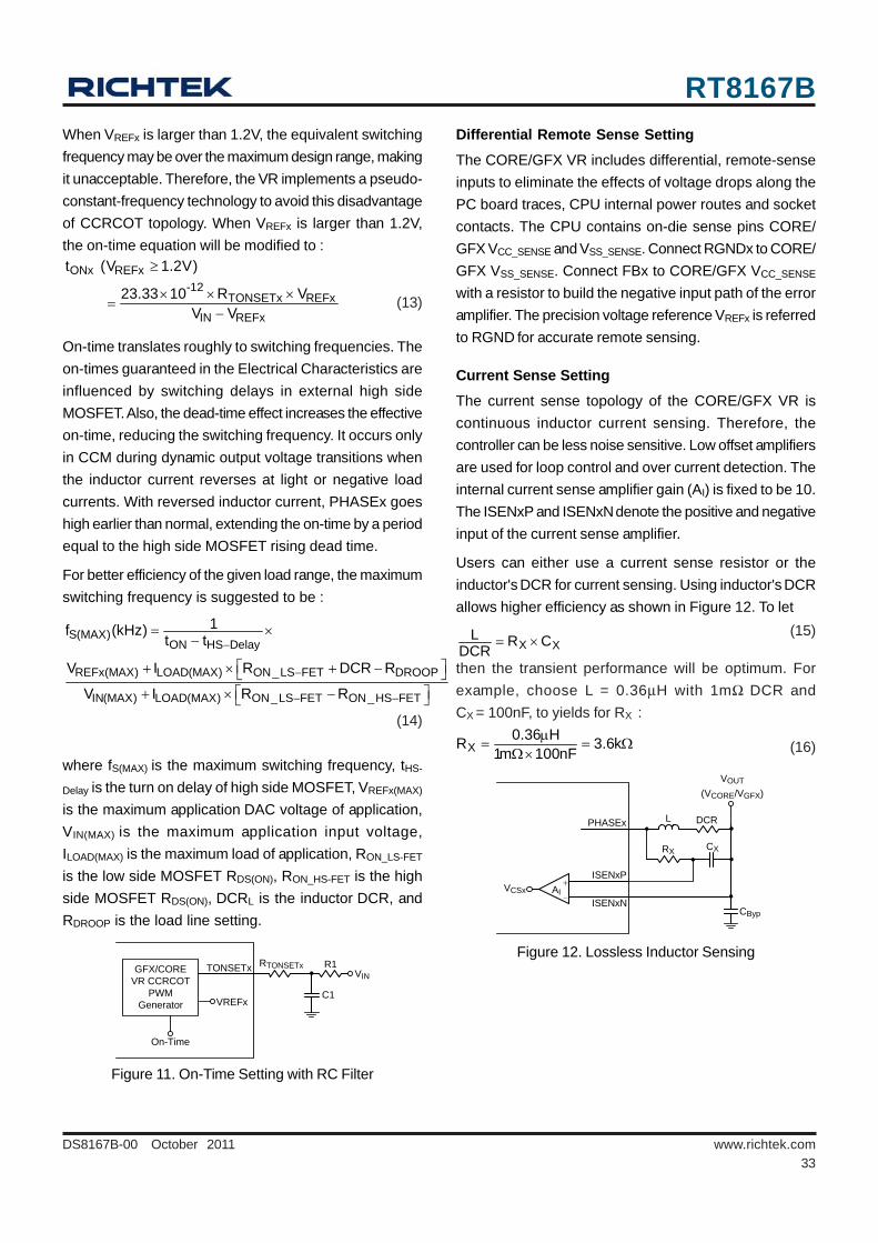
Figure 11. On-Time Setting with RC Filter
(13)
≥
× × ×=
−
ONx REFx-12
TONSETx REFxIN REFx
t (V 1.2V)
23.33 10 R V V V
(14)
−
−
− −
= ×−
⎡ ⎤+ × + −⎣ ⎦⎡ ⎤+ × −⎣ ⎦
S(MAX)ON HS Delay
REFx(MAX) LOAD(MAX) ON_LS FET DROOP
IN(MAX) LOAD(MAX) ON_LS FET ON_HS FET
1f (kHz)t t
V I R DCR R
V I R R
When VREFx is larger than 1.2V, the equivalent switchingfrequency may be over the maximum design range, makingit unacceptable. Therefore, the VR implements a pseudo-constant-frequency technology to avoid this disadvantageof CCRCOT topology. When VREFx is larger than 1.2V,the on-time equation will be modified to :
On-time translates roughly to switching frequencies. Theon-times guaranteed in the Electrical Characteristics areinfluenced by switching delays in external high sideMOSFET. Also, the dead-time effect increases the effectiveon-time, reducing the switching frequency. It occurs onlyin CCM during dynamic output voltage transitions whenthe inductor current reverses at light or negative loadcurrents. With reversed inductor current, PHASEx goeshigh earlier than normal, extending the on-time by a periodequal to the high side MOSFET rising dead time.
For better efficiency of the given load range, the maximumswitching frequency is suggested to be :
where fS(MAX) is the maximum switching frequency, tHS-
Delay is the turn on delay of high side MOSFET, VREFx(MAX)
is the maximum application DAC voltage of application,VIN(MAX) is the maximum application input voltage,ILOAD(MAX) is the maximum load of application, RON_LS-FET
is the low side MOSFET RDS(ON), RON_HS-FET is the highside MOSFET RDS(ON), DCRL is the inductor DCR, andRDROOP is the load line setting.
GFX/CORE VR CCRCOT
PWM Generator
TONSETx RTONSETx R1
C1
VIN
VREFx
On-Time
Differential Remote Sense SettingThe CORE/GFX VR includes differential, remote-senseinputs to eliminate the effects of voltage drops along thePC board traces, CPU internal power routes and socketcontacts. The CPU contains on-die sense pins CORE/GFX VCC_SENSE and VSS_SENSE. Connect RGNDx to CORE/GFX VSS_SENSE. Connect FBx to CORE/GFX VCC_SENSE
with a resistor to build the negative input path of the erroramplifier. The precision voltage reference VREFx is referredto RGND for accurate remote sensing.
Current Sense SettingThe current sense topology of the CORE/GFX VR iscontinuous inductor current sensing. Therefore, thecontroller can be less noise sensitive. Low offset amplifiersare used for loop control and over current detection. Theinternal current sense amplifier gain (AI) is fixed to be 10.The ISENxP and ISENxN denote the positive and negativeinput of the current sense amplifier.
Users can either use a current sense resistor or theinductor's DCR for current sensing. Using inductor's DCRallows higher efficiency as shown in Figure 12. To let
then the transient performance will be optimum. Forexample, choose L = 0.36μH with 1mΩ DCR andCX = 100nF, to yields for RX :
X XL R C
DCR= ×
(15)
X0.36 HR 3.6k
1m 100nFμ= = Ω
Ω× (16)
L DCR
RX CX
VOUT(VCORE/VGFX)
CByp
+
-
ISENxP
ISENxN
PHASEx
AIVCSx
Figure 12. Lossless Inductor Sensing
RT8167B
34DS8167B-00 October 2011www.richtek.com
Considering the inductance tolerance, the resistor RX hasto be tuned on board by examining the transient voltage.If the output voltage transient has an initial dip below theminimum load line requirement with a slow recovery, RX
is too small. Vice versa, if the resistance is too large theoutput voltage transient will only have a small initial dipand the recovery will be too fast, causing a ring-back.
Using current-sense resistor in series with the inductorcan have better accuracy, but the efficiency is a trade-off.Considering the equivalent inductance (LESL) of the currentsense resistor, a RC filter is recommended. The RC filtercalculation method is similar to the above-mentionedinductor DCR sensing method.
Operation Mode TransitionThe RT8167B supports operation mode transition functionin CORE/GFX VR for the SetPS command of Intel's VR12/IMVP7 CPU. The default operation mode of the RT8167B'sCORE/GFX VR is PS0, which is CCM operation. The otheroperation mode is PS2 (DEM operation).
After receiving SetPS command, the CORE/GFX VR willimmediately change to the new operation state. WhenVR receives SetPS command of PS2 operation mode,the VR operates as a DEM controller.
If VR receives dynamic VID change command (SetVID),VR will automatically enter PS0 operation mode. Afteroutput voltage reaches target voltage, VR will stay at PS0state and ignore former SetPS command. Only byre-sending SetPS command after SetVID command willVR be forced into PS2 operation state again.
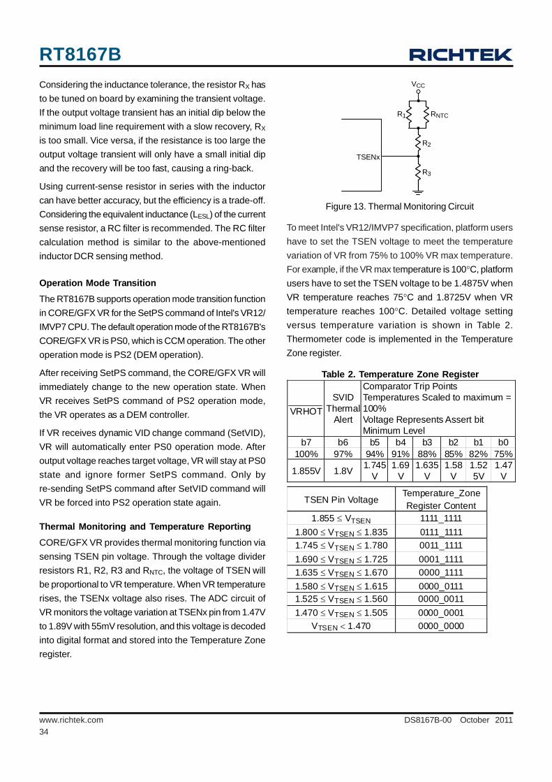
Thermal Monitoring and Temperature ReportingCORE/GFX VR provides thermal monitoring function viasensing TSEN pin voltage. Through the voltage dividerresistors R1, R2, R3 and RNTC, the voltage of TSEN willbe proportional to VR temperature. When VR temperaturerises, the TSENx voltage also rises. The ADC circuit ofVR monitors the voltage variation at TSENx pin from 1.47Vto 1.89V with 55mV resolution, and this voltage is decodedinto digital format and stored into the Temperature Zoneregister.
Figure 13. Thermal Monitoring Circuit
To meet Intel's VR12/IMVP7 specification, platform usershave to set the TSEN voltage to meet the temperaturevariation of VR from 75% to 100% VR max temperature.For example, if the VR max temperature is 100°C, platformusers have to set the TSEN voltage to be 1.4875V whenVR temperature reaches 75°C and 1.8725V when VRtemperature reaches 100°C. Detailed voltage settingversus temperature variation is shown in Table 2.Thermometer code is implemented in the TemperatureZone register.
TSENx
VCC
R1
R2
R3
RNTC
Table 2. Temperature Zone Register
VRHOT SVID
Thermal Alert
Comparator Trip Points Temperatures Scaled to maximum = 100% Voltage Represents Assert bit Minimum Level
b7 b6 b5 b4 b3 b2 b1 b0 100% 97% 94% 91% 88% 85% 82% 75%
1.855V 1.8V 1.745V
1.69V
1.635V
1.58V
1.525V
1.47V
TSEN Pin Voltage
Temperature_Zone Register Content
1.855 ≤ VTSEN 1111_1111 1.800 ≤ VTSEN ≤ 1.835 0111_1111 1.745 ≤ VTSEN ≤ 1.780 0011_1111 1.690 ≤ VTSEN ≤ 1.725 0001_1111 1.635 ≤ VTSEN ≤ 1.670 0000_1111 1.580 ≤ VTSEN ≤ 1.615 0000_0111 1.525 ≤ VTSEN ≤ 1.560 0000_0011 1.470 ≤ VTSEN ≤ 1.505 0000_0001
VTSEN < 1.470 0000_0000
RT8167B
35DS8167B-00 October 2011 www.richtek.com
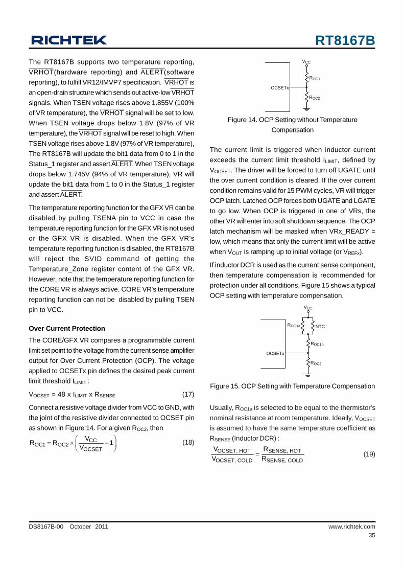
Figure 15. OCP Setting with Temperature Compensation
OCSETx
VCC
ROC1b
ROC2
ROC1a NTC
Usually, ROC1a is selected to be equal to the thermistor'snominal resistance at room temperature. Ideally, VOCSET
is assumed to have the same temperature coefficient asRSENSE (Inductor DCR) :
OCSET, HOT SENSE, HOT
OCSET, COLD SENSE, COLD
V RV R
= (19)
(18)CCOC1 OC2
OCSET
VR R 1V
⎛ ⎞= × −⎜ ⎟⎝ ⎠
Figure 14. OCP Setting without TemperatureCompensation
VCC
OCSETx
ROC1
ROC2
The current limit is triggered when inductor currentexceeds the current limit threshold ILIMIT, defined byVOCSET. The driver will be forced to turn off UGATE untilthe over current condition is cleared. If the over currentcondition remains valid for 15 PWM cycles, VR will triggerOCP latch. Latched OCP forces both UGATE and LGATEto go low. When OCP is triggered in one of VRs, theother VR will enter into soft shutdown sequence. The OCPlatch mechanism will be masked when VRx_READY =low, which means that only the current limit will be activewhen VOUT is ramping up to initial voltage (or VREFx).
If inductor DCR is used as the current sense component,then temperature compensation is recommended forprotection under all conditions. Figure 15 shows a typicalOCP setting with temperature compensation.
Over Current ProtectionThe CORE/GFX VR compares a programmable currentlimit set point to the voltage from the current sense amplifieroutput for Over Current Protection (OCP). The voltageapplied to OCSETx pin defines the desired peak currentlimit threshold ILIMIT :
VOCSET = 48 x ILIMIT x RSENSE (17)
Connect a resistive voltage divider from VCC to GND, withthe joint of the resistive divider connected to OCSET pinas shown in Figure 14. For a given ROC2, then
The RT8167B supports two temperature reporting,VRHOT(hardware reporting) and ALERT(softwarereporting), to fulfill VR12/IMVP7 specification. VRHOT isan open-drain structure which sends out active-low VRHOTsignals. When TSEN voltage rises above 1.855V (100%of VR temperature), the VRHOT signal will be set to low.When TSEN voltage drops below 1.8V (97% of VRtemperature), the VRHOT signal will be reset to high. WhenTSEN voltage rises above 1.8V (97% of VR temperature),The RT8167B will update the bit1 data from 0 to 1 in theStatus_1 register and assert ALERT. When TSEN voltagedrops below 1.745V (94% of VR temperature), VR willupdate the bit1 data from 1 to 0 in the Status_1 registerand assert ALERT.
The temperature reporting function for the GFX VR can bedisabled by pulling TSENA pin to VCC in case thetemperature reporting function for the GFX VR is not usedor the GFX VR is disabled. When the GFX VR'stemperature reporting function is disabled, the RT8167Bwill reject the SVID command of getting theTemperature_Zone register content of the GFX VR.However, note that the temperature reporting function forthe CORE VR is always active. CORE VR's temperaturereporting function can not be disabled by pulling TSENpin to VCC.
RT8167B
36DS8167B-00 October 2011www.richtek.com
According to the basic circuit calculation, VOCSET can beobtained at any temperature :
OC2OCSET, T CC
OC1a NTC, T OC1b OC2
RV VR / /R R R
= ×+ +
(20)
Re-write (19) from (20), to get VOCSET at room temperature
OC1a NTC, COLD OC1b OC2 SENSE, HOT
OC1a NTC, HOT OC1b OC2 SENSE, COLD
R //R R R RR //R R R R
+ +=
+ + (21)
(22)
OCSET, 25
OC2CC
OC1a NTC, 25 OC1b OC2
VR V
R / /R R R
=
×+ +
Solving (21) and (22) yields ROC1b and ROC2
(23)
OC2
EQU, HOT EQU, COLD EQU, 25
CCOCSET, 25
RR R (1 ) R
V (1 )
V
=α× − + − α ×
× − α
(24)
OC1b
EQU, HOT EQU, COLD
R( 1) R2 R R
(1 )
=α − × + α× −
− α
where
SENSE, HOT 25 HOTSENSE, COLD 25 COLD
R DCR [1 0.00393 (T 25)]R DCR [1 0.00393 (T 25)]
α =
× + × −=
× + × −
(25)
REQU, T = ROC1a // RNTC, T (26)
Over Voltage Protection (OVP)The over voltage protection circuit of CORE/GFX VRmonitors the output voltage via the ISENxN pin. Thesupported maximum operating VID of VR (V(MAX)) is storedin the Vout_Max register. Once VISENxN exceeds “V(MAX)
+ 200mV”, OVP is triggered and latched. VR will try toturn on low side MOSFETs and turn off high sideMOSFETs to protect CPU. When OVP is triggered bythe one of the VRs, the other VR will enter soft shutdownsequence. A 10μs delay is used in OVP detection circuitto prevent false trigger.
(27)IN OUTMIN ON
Ripple(MAX)
V VL tI
−= ×
Negative Voltage Protection (NVP)During OVP latch state, both CORE/GFX VRs also monitorISENxN pin for negative voltage protection. Since the OVPlatch will continuously turn on low side MOSFET of VR,VR may suffer negative output voltage. Therefore, whenthe voltage of ISENxN drops below −0.05V after triggeringOVP, VR will turn off low side MOSFETs while high sideMOSFETs remain off. The NVP function will be active onlyafter OVP is triggered.
Under Voltage Protection (UVP)Both CORE/GFX VR implement Under Voltage Protection(UVP). If ISENxN is less than VREFx by 300mV + VOFFSET,VR will trigger UVP latch. The UVP latch will turn off bothhigh side and low side MOSFETs. When UVP is triggeredby one of the VRs, the other VR will enter into softshutdown sequence. The UVP mechanism is maskedwhen VRx_READY = low.
Under Voltage Lock Out (UVLO)During normal operation, if the voltage at the VCC pindrops below UVLO falling edge threshold, both VR willtrigger UVLO. The UVLO protection forces all high sideMOSFETs and low side MOSFETs off to turn off.
Inductor SelectionThe switching frequency and ripple current determine theinductor value as follows :
where tON is the UGATE turn on period.
Higher inductance induces less ripple current and hencehigher efficiency. However, the tradeoff is a slower transientresponse of the power stage to load transients. This mightincrease the need for more output capacitors, thus drivingup the cost. Find a low-loss inductor having the lowestpossible DC resistance that fits in the allotted dimensions.The core must be large enough not to be saturated at thepeak inductor current.
RT8167B
37DS8167B-00 October 2011 www.richtek.com
Output Capacitor SelectionOutput capacitors are used to obtain high bandwidth forthe output voltage beyond the bandwidth of the converteritself. Usually, the CPU manufacturer recommends acapacitor configuration. Two different kinds of outputcapacitors can be found, bulk capacitors closely locatedto the inductors and ceramic output capacitors in closeproximity to the load. Latter ones are for mid-frequencydecoupling with very small ESR and ESL values while thebulk capacitors have to provide enough stored energy toovercome the low-frequency bandwidth gap between theregulator and the CPU.
Layout ConsiderationCareful PC board layout is critical to achieving lowswitching losses and clean, stable operation. Theswitching power stage requires particular attention. Ifpossible, mount all of the power components on the topside of the board with their ground terminals flushedagainst one another. Follow these guidelines for optimumPC board layout :
Keep the high current paths short, especially at theground terminals.
Keep the power traces and load connections short. Thisis essential for high efficiency.
When trade-offs in trace lengths must be made, it'spreferable to allow the inductor charging path to be madelonger than the discharging path.
Place the current sense component close to thecontroller. ISENxP and ISENxN connections for currentlimit and voltage positioning must be made using Kelvinsense connections to guarantee the current senseaccuracy. The PCB trace from the sense nodes shouldbe parallel to the controller.
Route high-speed switching nodes away from sensitiveanalog areas (COMPx, FBx, ISENxP, ISENxN, etc...)
Special attention should be paid in placing the DCRcurrent sensing components. The DCR current sensingcapacitor and resistors must be placed close to thecontroller.
The capacitor connected to the ISEN1N/ISENAN for noisedecoupling is optional and it should also be placed closeto the ISEN1N/ISENAN pin.
The NTC thermistor should be placed physically closeto the inductor for better DCR thermal compensation.
RT8167B
38DS8167B-00 October 2011www.richtek.com
Information that is provided by Richtek Technology Corporation is believed to be accurate and reliable. Richtek reserves the right to make any change in circuit
design, specification or other related things if necessary without notice at any time. No third party intellectual property infringement of the applications should be
guaranteed by users when integrating Richtek products into any application. No legal responsibility for any said applications is assumed by Richtek.
Richtek Technology CorporationHeadquarter5F, No. 20, Taiyuen Street, Chupei CityHsinchu, Taiwan, R.O.C.Tel: (8863)5526789 Fax: (8863)5526611
Richtek Technology CorporationTaipei Office (Marketing)5F, No. 95, Minchiuan Road, Hsintien CityTaipei County, Taiwan, R.O.C.Tel: (8862)86672399 Fax: (8862)86672377Email: [email protected]
Outline Dimension
Dimensions In Millimeters Dimensions In Inches Symbol
Min Max Min Max
A 0.700 0.800 0.028 0.031
A1 0.000 0.050 0.000 0.002
A3 0.175 0.250 0.007 0.010
b 0.150 0.250 0.006 0.010
D 4.950 5.050 0.195 0.199
D2 3.250 3.500 0.128 0.138
E 4.950 5.050 0.195 0.199
E2 3.250 3.500 0.128 0.138
e 0.400 0.016
L 0.350 0.450 0.014 0.018
W-Type 40L QFN 5x5 Package
Note : The configuration of the Pin #1 identifier is optional,but must be located within the zone indicated.
DETAIL APin #1 ID and Tie Bar Mark Options
11
2 2
D
E
D2
E2
L
b
A
A1A3
e
1
SEE DETAIL A