Embed Size (px)
Citation preview

Publication Date: May 2016
1
<Dual-In-Line Package Intelligent Power Module>
DIPIPM APPLICATION NOTE Bootstrap Circuit Design Manual
Table of contents
CHAPTER 1 Bootstrap Circuit Design ...................................................................................... 2 1.1 Bootstrap Circuit Operation ................................................................................................ 2 1.2 Initial charging ................................................................................................................... 2
1.2.1 Initial charging procedure ............................................................................................................ 2 1.2.2 Initial charging time ...................................................................................................................... 3 1.2.3 Voltage drop while suspending operation .................................................................................... 4
1.3 Charging in operation ........................................................................................................ 5 1.3.1 Basic charging scheme ............................................................................................................... 5 1.3.2 Charging scheme in the three phase modulation sine wave control operation ........................... 7 1.3.3 Effects on charging situation due to driving conditions ............................................................... 9 1.3.4 Estimation method of capacitance of BSC ................................................................................13 1.3.5 Design for current limiting resistor .............................................................................................13 1.3.6 Note for designing the bootstrap circuit .....................................................................................15
1.4 Circuit currents in the case of other control methods ....................................................... 16
-End part- Revision record Note about safety design and using this material

<Dual-In-Line Package Intelligent Power Module> Application Note Bootstrap Circuit Design Manual
Publication Date: May 2016
2
CHAPTER 1 Bootstrap Circuit Design 1.1 Bootstrap Circuit Operation
For three phase inverter circuit driving, normally four isolated control supplies (three for P-side driving and one for
N-side driving) are necessary. But using floating control supply with bootstrap circuit can reduce the number of isolated control supplies from four to one (N-side control supply).
Bootstrap circuit consists of a bootstrap diode(BSD), a bootstrap capacitor(BSC) and a current limiting resistor. (Fig.1-1) It uses the BSC as a control supply for driving P-side device such as IGBT and MOSFET. The BSC supplies gate charge when P-side device turning ON and circuit current of logic circuit on P-side driving IC. (Fig.1-2) Since a capacitor is used as substitute for isolated supply, its supply capability is limited. This floating supply driving with bootstrap circuit is suitable for small supply current products like DIPIPM.
Charge consumed by driving circuit is re-charged from N-side 15V control supply to BSC via current limiting resistor and BSD when voltage of output terminal (U, V or W) goes down to GND potential in inverter operation. But there is the possibility that enough charge doesn't perform due to the conditions such as switching sequence, capacitance of BSC, current limiting resistance and so on. Deficient charge leads to low voltage of BSC and might work under voltage protection (UV). This situation makes the loss of P-side device increase by low gate voltage or stop switching. So it is necessary to consider and evaluate enough for designing bootstrap circuit.
Fig.1-1 Bootstrap Circuit Diagram Fig.1-2 Bootstrap Circuit Diagram
1.2 Initial charging
1.2.1 Initial charging procedure In the case of applying bootstrap circuit, it is necessary to charge to the BSC initially because voltage of BSC is 0V
at initial state or it may go down to the trip level of under voltage protection after long suspending period (even 1s). BSC charging is performed by turning on all N-side IGBT normally.(Fig. 1-3) When outer load (e.g. motor) is connected to DIPIPM, BSC charging may be performed by turning on only one phase N-side IGBT since potential of all output terminals will go down to GND level through the wiring in the motor. But its charging efficiency might become lower due to some reason. (e.g. wiring resistance of motor) (Fig. 1-4)
There are mainly two procedures for BSC charging. One is performed by one long pulse, and another is conducted by multiple short pulses. Multi pulse method is used when there are some restriction like control supply capability, forward surge current of BSD, power rating of current limiting resistor and so on. Enough long pulse is needed for initial charge.
Bootstrap diode (BSD)
Bootstrap capacitor (BSC)
Current limiting resistor
N(GND)
P(Vcc)
U,V,W
VD=15V N-side IGBT
P-side IGBT
VFB
VFS
HVIC
LVIC
↑High voltage area
VN1
VNC
VP1 P-side FWDi
N-side FWDi
Level Shift
VPC
+
Voltage of VFS that is reference voltage of BSC swings between VCC and GND level. If voltage of BSC is lower than 15V when VFS becomes to GND potential, BSC is charged from 15V N-side control supply.
BSD
P(Vcc)
U,V,W
P-side IGBT
VFB
VFS
Gate D
rive
Logic & U
V protection
Level Shift
15V
Low voltage area
VP1
P-side FWDi
BSC
VPC
+

<Dual-In-Line Package Intelligent Power Module> Application Note Bootstrap Circuit Design Manual
Publication Date: May 2016
3
Fig.1-3 Initial charging root Fig.1-4 Charging root at turning on one phase
Fig.1-5 Example of waveform by one charging pulse Fig.1-6 Example of waveform by multiple charging pulses
1.2.2 Initial charging time
Time required for initial charge depends on capacitance of BSC, forward voltage of BSD and limiting resistance.
Charge is performed with time constant that is roughly calculated from capacitance of BSC and limiting resistance. Example of calculated charging waveform is described in Fig.1-7. Sample: Super mini DIPIPM Ver.5 PS219B2
(5A/600V, BSD and limiting resistor(100Ω) are integrated), Condition: BSC=22μF or 100μF, VD=15V
Fig.1-7 Example of initial charging
As above figure, voltage of BSC doesn't saturate (about 60%) by charging up to time constant (e.g. τ=C x R=22μF x
100Ω=2.2ms). For saturated charge, about sixfold period of time constant will be needed. Saturated voltage doesn't reach to the control voltage VD. It will become about 1.2V lower than control supply voltage (typ. 15V) due to voltage drops of N-side IGBT (VCE(sat)) and BSD (VF) which are in charging path. Refer Fig.1-3
0
2
4
6
8
10
12
14
16
0 0.01 0.02 0.03 0.04 0.05 0.06 0.07
Time(s)
Vol
tage
of B
SC
(V)
22μF100μF
Timeconstant
Saturates at sixfold period oftime constant in each case.
0V VD
15V
0V
N-side input
0
Charge current
0
Voltage of BSC VDB
0V VD
15V
0V
0
0
N-side input
Charge current
Voltage of BSC VDB
P(Vcc)
N(GND)
BSD
15V
VFB
VFS
LVIC
VN1
VNC
VP1
VPC
HVIC
HVIC
U V
W ON OFF OFF
Level Shift
HVIC
+ + +
P(Vcc)
N(GND)
BSD
U,V,W
15V N-side IGBT
P-side IGBT
VFB
VFS HVIC
LVIC
VN1
VNC
VP1
N-side FWDi
Level Shift
VPC
VDB
ON
+

<Dual-In-Line Package Intelligent Power Module> Application Note Bootstrap Circuit Design Manual
Publication Date: May 2016
4
Initial charging needs to be performed until voltage of BSC exceeds recommended minimum supply voltage 13V. (It is recommended to charge as high as possible with consideration for voltage drop between the end of charging and start of inverter operation.)
After BSC was charged, it is recommended to input one ON pulse to the P-side input for reset of internal IC state before starting system. Necessary width is allowable minimum input pulse width PWIN(on) or more. (e.g. 0.7μs or more for Super mini DIP Ver.5 PS219B2. Refer the datasheet for each product. )
1.2.3 Voltage drop while suspending operation
Voltage of BSC also drops gradually due to circuit current of control IC while suspending operation. Its drop rate will
be estimated by the calculation from capacitance C of BSC and steady circuit current IDB of P-side control IC (e.g. maximum 0.1mA for Super mini DIP Ver.5 PS219B2. It is different by products. Refer the datasheet for each product.)
Voltage drop ΔV= IDB x t / C (t: discharging time)
When stopped state continues for long time and VDB drops below 13V (=recommended minimum control voltage for
VDB), it is necessary to recharge to BSC before starting operation. Example of voltage drop calculation for Super mini DIP Ver.5 is shown in Fig.1-8. Conditions: Initial voltage of BSC=15V, Circuit current IDB=0.1mA, BSC=22 and 100μF
Fig.1-8 Example of voltage drop of BSC in suspended time
When stopped state continues over 0.44s in the case of 22μF, recharging will be required before restart. If it
continues over 0.7s, VDB will drop below 12V and under voltage protection may work. This example is the calculation result. It is necessary to evaluate in the real system finally.
0.440123456789
10111213141516
0.0 0.5 1.0 1.5 2.0
Stop time(s)
Vol
tage
of B
SC(
V)
22μF
100μF

<Dual-In-Line Package Intelligent Power Module> Application Note Bootstrap Circuit Design Manual
Publication Date: May 2016
5
1.3 Charging in operation
1.3.1 Basic charging scheme Charge of bootstrap capacitor (BSC), which was consumed by circuit current (e.g. gate charge for P-side IGBT) in
the inverter operation by PWM signal like three phase modulation sine wave control, is recharged through bootstrap diode (BSD) when voltage potential VFB of VFB terminal becomes lower than 15V control supply due to the output terminal (e.g. U,V,W) drops to about GND level in the case of N-side IGBT turning on period or free whiling period after P-side IGBT turning off.
But practically the charge current starts flowing when voltage potential VFB is about 0.6V lower than N-side control supply 15V because BSD needs to turn on. (Fig. 1-9, 10)
Fig.1-9 Charging situation
Fig.1-10 Charge current with limiting resistor Because potential of output terminal varies depending on the direction of motor current flow or the device IGBT or
FWDi of N-side into which the current flows, voltage potential VFB also varies. So BSC is not always charged when IGBT or FWDi of N-side turns on. Charging situation is explained below.
There are below two modes of charging situation in inverter operation.
Mode 1: Free wheeling situation of N-side FWDi after P-side turning off Mode 2: Current flowing situation into N-side IGBT
Current flows chart at both modes is illustrated in Fig.1-11. Charge mode is decided by output current direction.
(Fig.1-12)
Vcc
VFB≈VDB
15V
GND Control supply
BSC ≈GND
BSC is charged when VFB is about 0.6V lower than control supply.
P-side IGBT ON P-side FWDi ON
N-side IGBT ON N-side FWDi ON
BSC
VDB
VDB
Transition by switching
VFB=Vcc+VDB BSC cannot be charged, because VFB is higher than control supply 15V.
Control supply
VF-IF curve of BSD
Charge current flows depending on the voltage between both ends of BSD and resistor.
Voltage between both ends of BSD and resistor
Cha
rge
curre
nt
・Charge current flows when voltage of both ends exceeds about 0.6V.
・Charge efficiency boosts up increasingly when voltage of both ends becomes larger since charge current increases.
≈0.6V
VF-IF curve + R x i (Voltage drop by limiting resistor is added to VF-IF curve)
Potential of output terminal becomes about GND level in the case of N-side IGBT or N-side FWDi turning on by free wheeling
VFB: Voltage potential of VFB terminal based on GND level VDB: Charged voltage in BSC
P(Vcc)
N(GND)
BSD
U,V,W
15V N-side IGBT
P-side IGBT
VFB
VFS HVIC
LVIC
VN1
VNC
VP1
N-side FWDi
Level Shift
VPC
VDB
ON
+

<Dual-In-Line Package Intelligent Power Module> Application Note Bootstrap Circuit Design Manual
Publication Date: May 2016
6
Fig.1-11 Charging mode in the case that currents flows from U to V phase
Fig.1-12 Relation between output current waveform and charging mode The potential voltage of output terminal (i.e. reference voltage of BSC) depends on forward voltage VEC(i) at mode1
or saturation voltage of IGBT VCEsat(i) and voltage drop by shunt resistor R x i at mode2 as below.
Mode 1: Voltage of output terminal=GND potential (0V) - VEC(i) <0V Mode 2: Voltage of output terminal=GND potential (0V) + VCEsat(i) + R x i >0V
Because VDB (voltage by charge stored in BSC) goes by voltage of output terminal, voltage potential VBSC of BSC
becomes as below. (Refer Fig. 1-13 too.)
Mode 1 : VFB =VDB-VEC(i) Mode 2 : VFB =VDB+VCEsat(i)+R x i
Fig.1-13 Difference of potential VBSC due to charging modes
0 time
Mode1 charging status Current flows out from output terminal.
Mode 2 charging status Current flows into output terminal.
VFB: Voltage potential of VFB terminal based on GND level VDB: Charged voltage in BSC
VEC(i) (Change by current)
Control supply
15V
VDB
VFB (Change by VEC(i))
GND
BSC
VCEsat(i) (Change by current)
VDB
VFB(Change by VCE(sat)(i), R x i)
Mode 2
BSC
R x i Voltage drop by shunt resistor (Change by current)
Voltage potential of Output terminal
Mode 1
If difference between control supply voltage 15V and VFB is about 0.6V or more, BSD turns on and charging starts.
Control supply Voltage potential of
Output terminal
[Mode1] Potential of U terminal drops to about GND level and charge starts when N-side FWDi turns on due to free wheeling current after P-side IGBT turning off.
[Mode 2] Potential of V terminal drops to about GND level and charge starts when N-side IGBT turns on.
Shunt resistor R
P(Vcc) BSD
U
VD=15V
VFB
VFS
HVIC
LVIC
VN1
VNC
VP1
VPC
VDB
ONOFF
N(GND)
BSD
V
VD=15V
P-side IGBT
VFB
VFS
HVIC
LVIC
VN1
VNC
VP1
VPC
VDB
ON
M
+
P-side IGBT
VEC(i) VCEsat(i)
R x i
+
<Dual-In-Line Package Intelligent Power Module> Application Note Bootstrap Circuit Design Manual
Publication Date: May 2016
7
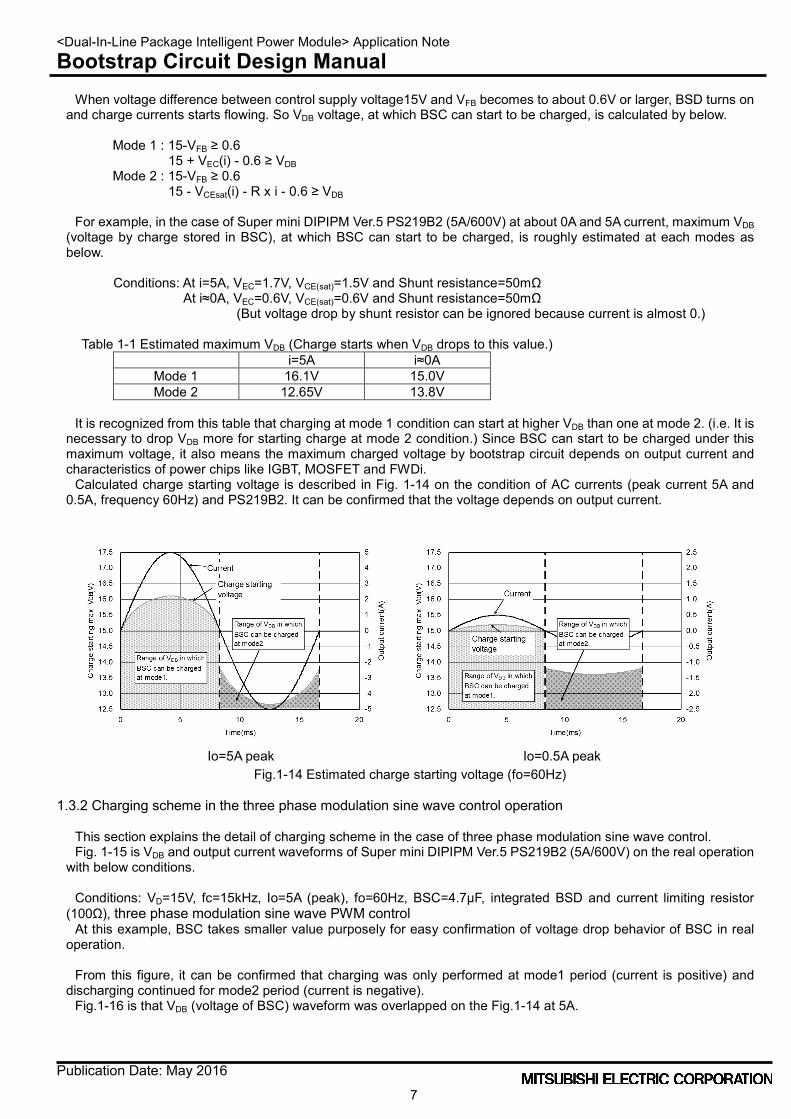
When voltage difference between control supply voltage15V and VFB becomes to about 0.6V or larger, BSD turns on and charge currents starts flowing. So VDB voltage, at which BSC can start to be charged, is calculated by below.
Mode 1 : 15-VFB ≥ 0.6 15 + VEC(i) - 0.6 ≥ VDB Mode 2 : 15-VFB ≥ 0.6 15 - VCEsat(i) - R x i - 0.6 ≥ VDB
For example, in the case of Super mini DIPIPM Ver.5 PS219B2 (5A/600V) at about 0A and 5A current, maximum VDB
(voltage by charge stored in BSC), at which BSC can start to be charged, is roughly estimated at each modes as below.
Conditions: At i=5A, VEC=1.7V, VCE(sat)=1.5V and Shunt resistance=50mΩ
At i≈0A, VEC=0.6V, VCE(sat)=0.6V and Shunt resistance=50mΩ (But voltage drop by shunt resistor can be ignored because current is almost 0.)
Table 1-1 Estimated maximum VDB (Charge starts when VDB drops to this value.)
i=5A i≈0A Mode 1 16.1V 15.0V Mode 2 12.65V 13.8V
It is recognized from this table that charging at mode 1 condition can start at higher VDB than one at mode 2. (i.e. It is
necessary to drop VDB more for starting charge at mode 2 condition.) Since BSC can start to be charged under this maximum voltage, it also means the maximum charged voltage by bootstrap circuit depends on output current and characteristics of power chips like IGBT, MOSFET and FWDi.
Calculated charge starting voltage is described in Fig. 1-14 on the condition of AC currents (peak current 5A and 0.5A, frequency 60Hz) and PS219B2. It can be confirmed that the voltage depends on output current.
Io=5A peak Io=0.5A peak
Fig.1-14 Estimated charge starting voltage (fo=60Hz)
1.3.2 Charging scheme in the three phase modulation sine wave control operation This section explains the detail of charging scheme in the case of three phase modulation sine wave control. Fig. 1-15 is VDB and output current waveforms of Super mini DIPIPM Ver.5 PS219B2 (5A/600V) on the real operation
with below conditions. Conditions: VD=15V, fc=15kHz, Io=5A (peak), fo=60Hz, BSC=4.7μF, integrated BSD and current limiting resistor
(100Ω), three phase modulation sine wave PWM control At this example, BSC takes smaller value purposely for easy confirmation of voltage drop behavior of BSC in real
operation. From this figure, it can be confirmed that charging was only performed at mode1 period (current is positive) and
discharging continued for mode2 period (current is negative). Fig.1-16 is that VDB (voltage of BSC) waveform was overlapped on the Fig.1-14 at 5A.

<Dual-In-Line Package Intelligent Power Module> Application Note Bootstrap Circuit Design Manual
Publication Date: May 2016
8
Voltage of BSC VDB(1V/div)
Output current(5A/div) VDB
Charging
Charging period
15V
0A
Discharging
Fig.1-15 Example waveform in charging Fig.1-16 Charging situation Fig. 1-16 suggests that BSC can be charged at positive current period (Mode 1) but for negative current period, it
cannot be charged because voltage of BSC VDB is higher than charge starting voltage. So BSC will be almost charged in Mode 1 region (Positive current and free wheeling to N-side FWDi) except for particular condition like quite small BSC capacitance. Here there are the not-charged periods despite VDB is lower than charge starting voltage. (part A & B in Fig.1-16) The reasons are estimated as below.
At part A, the voltage difference between voltage of BSC VDB and charge starting voltage becomes smaller (i.e. the voltage applied to BSD becomes small), hence charging current that flows into BSC also decreases. It leads to VDB drop because discharge amount exceeds charge amount.
At part B, the voltage difference between voltage of BSC VDB and charge starting voltage is enough large, so charging current that flows into BSC enough large. But charging time is quit short because ON duty of N-side FWDi (=OFF duty of P-side IGBT) is almost 0 in this moment. It leads to small charge amount per one switching operation.
So efficiency of charge is also affected by duty of PWM control signal (i.e. power factor (phase delay between current and voltage) and modulation rate). (Fig.1-17)
Fig.1-17 Effect on charging due to the phase difference between PWM signal and current Charging to BSC is also affected by other inverter driving conditions. From here effects on charging situation due to
driving condition by three phase modulation sine wave control are explained with simulation waveforms.
12.5
13.0
13.5
14.0
14.5
15.0
15.5
16.0
16.5
17.0
17.5
0 5 10 15 20
Time(ms)
Cha
rge
star
ting
max
. VD
B(V)
-5
-4
-3
-2
-1
0
1
2
3
4
5
Out
put c
urre
nt(A
)
Current
Charge startingvoltage
Measured VDB
BSC cannot be charged since VDB exceeds charge starting voltage.
B
A
0 time
Output current
Output voltage
P-side IGBT input ON duty 0
0.5 P-side IGBT input OFF duty =N-side FWDi ON duty
Power factor cos Φ
VDB
Charge
1
Mode1 reagion
Discharge
Charge amount per every carrier frequency in positive current region is calculated by below formula. Charge current x ON time of N-side FWDi So charge amount becomes small in this region.

<Dual-In-Line Package Intelligent Power Module> Application Note Bootstrap Circuit Design Manual
Publication Date: May 2016
9
1.3.3 Effects on charging situation due to driving conditions To consider effects on charging situation by driving conditions, the results of simulation of VDB with various conditions
are described as below. Those conditions are
[Common conditions] IPM: Super mini DIPIPM Ver.5 PS219B2 (5A/600V), BSC=4.7μF, Io=5A(peak), fc=15kHz, fo=20Hz, P.F=0.8, Modulation rate=0.7, VD=15V, Shunt resistance 50mΩ, three phase modulation sine wave control
[Comparative conditions] (Common conditions are used if not otherwise noted.) (1) Output frequency : fo=20Hz, 60Hz and 120Hz (2) Carrier frequency : fc=15kHz and 5kHz (3) Capacitance of BSC : BSC=1μF, 4.7μF and 22μF (4) Output current : Io=5A peak and 2A peak (fo=60Hz and 20Hz)
(1) Comparison of output frequency: fo=20Hz, 60Hz and 120Hz
The results of simulation with three conditions of output frequency are charted in Fig.1-18, 19 and 20. At 20Hz, time of one cycle becomes long and the period of Mode 2, at which charging is not performed easily, becomes long too. Then voltage VDB drops to under 13V: recommended minimum control voltage for VDB of DIPIPM. (In this case charging at Mode 2 is performed partly because VDB drops excessively. part A in Fig.1-19)
On the other hand at 120Hz, time of one cycle is short, so VDB drop becomes small. But charging time at Mode 1 becomes short in parallel. Then maximum charged voltage is lower than one at 20Hz. But the ripple of voltage becomes smaller than one at 20Hz.
If there is the low output frequency operation in your system and capacitance of BSC isn't suitable value, there is the possibility of increasing loss or system stop by working under voltage protection due to excessive drop of VDB. It is necessary to evaluate well when designing circuit.
Fig.1-18 fo=60Hz Fig.1-19 fo=20Hz
Fig.1-20 fo=120Hz
-15
-10
-5
0
5
10
15
0.000 0.010 0.020 0.030 0.040 0.050 0.060
Time(s)
Out
put c
urre
nt(A
)
11
12
13
14
15
16
17
Vol
tage
of B
SC
(V)
Max 15.68VAve 15.08VMin 14.40VRipple 1.28V
Voltage of BSC
-15
-10
-5
0
5
10
15
0.000 0.010 0.020 0.030 0.040 0.050 0.060
Time(s)
Out
put c
urre
nt(A
)
11
12
13
14
15
16
17
Vol
tage
of B
SC
(V)
Max 15.81VAve 14.51VMin 12.77VRipple 3.04V
Voltage of BSC
-15
-10
-5
0
5
10
15
0.000 0.010 0.020 0.030 0.040 0.050 0.060
Time(s)
Out
put c
urre
nt(A
)
11
12
13
14
15
16
17
Vol
tage
of B
SC
(V)
Max 15.56VAve 15.23VMin 14.94VRipple 0.62V
Voltage of BSC
A
Because discharging time is long, voltage drop becomes large.

<Dual-In-Line Package Intelligent Power Module> Application Note Bootstrap Circuit Design Manual
Publication Date: May 2016
10
(2) Comparison of carrier frequency: fc=15kHz and 5kHz
The results of simulation with two conditions of carrier frequency are charted in Fig.1-21 and 22. When carrier frequency increases, amount of gate charge (circuit current) increases according to frequency. Then voltage drop of BSC also increases depending on carrier frequency fc. So it is necessary to increase the capacitance of BSC generally in the case of high frequency operation.
Fig.1-21 fc=15kHz Fig.1-22 fc=5kHz
Typical circuit current vs. carrier frequency characteristics of Super mini DIPIPM Ver.5 PS219B2 (5A/600V), which is
used to above simulations, is charted in Fig.1-23. It indicates circuit current is large at high frequency. Since circuit current increases according to amount of gate charge, the high current rating products (i.e. they have
large gate capacitance) generally consume larger circuit current and it is necessary to consider the capacitance of BSC.
This circuit current vs. carrier frequency characteristics is prepared for all DIPIPM series. Please refer the
application note for each product.
Conditions: VD=VDB=15V, Tj=125°C, IGBT ON Duty=10, 30, 50, 70, 90%
Fig.1-23 Circuit current IDB vs. carrier frequency characteristics for PS219B2 (Typical data)
-15
-10
-5
0
5
10
15
0.000 0.010 0.020 0.030 0.040 0.050 0.060
Time(s)
Out
put c
urre
nt(A
)
11
12
13
14
15
16
17
Vol
tage
of B
SC
(V)
Max 15.81VAve 14.51VMin 12.77VRipple 3.04V
Voltage of BSC
-15
-10
-5
0
5
10
15
0.000 0.010 0.020 0.030 0.040 0.050 0.060
Time(s)O
utpu
t cur
rent
(A)
11
12
13
14
15
16
17
Vol
tage
of B
SC
(V)
Max 15.94VAve 15.19VMin 14.13VRipple 1.81V
Voltage of BSC

<Dual-In-Line Package Intelligent Power Module> Application Note Bootstrap Circuit Design Manual
Publication Date: May 2016
11
(3) Comparison of capacitance of BSC: BSC=1μF, 4.7μF and 22μF
The results of simulation with three conditions of capacitance of BSC are charted in Fig.1-24~1-26. When capacitance of BSC is quite small, voltage drop of BSC increases considerably. Then the lower limit voltage of VDB drops extremely and its ripple voltage becomes larger. For DIPIPM recommended value of VDB ripple is within 2Vp-p.
Fig.1-24 BSC=4.7μF Fig.1-25 BSC=1.0μF
Fig.1-26 BSC=22μF
-15
-10
-5
0
5
10
15
0.000 0.010 0.020 0.030 0.040 0.050 0.060
Time(s)
Out
put c
urre
nt(A
)
11
12
13
14
15
16
17
Vol
tage
of B
SC
(V)
Max 15.81VAve 14.51VMin 12.77VRipple 3.04V
Voltage of BSC
-15
-10
-5
0
5
10
15
0.000 0.010 0.020 0.030 0.040 0.050 0.060
Time(s)O
utpu
t cur
rent
(A)
11
12
13
14
15
16
17
Vol
tage
of B
SC
(V)
Max 15.83VAve 14.22VMin 12.56VRipple 3.27V
Voltage of BSC
-15
-10
-5
0
5
10
15
0.000 0.010 0.020 0.030 0.040 0.050 0.060
Time(s)
Out
put c
urre
nt(A
)
11
12
13
14
15
16
17
Vol
tage
of B
SC
(V)
Max 15.60VAve 15.19VMin 14.80VRipple 0.80V
Voltage of BSC

<Dual-In-Line Package Intelligent Power Module> Application Note Bootstrap Circuit Design Manual
Publication Date: May 2016
12
(4) Comparison of output current: Io=5A peak and 2A peak (fo=60Hz and 20Hz)
The results of simulation with four conditions of output current are charted in Fig.1-27~1-30. As described above section 1.3.1, charge starting voltage changes depending on output current. When output current is small, charge starting voltage drops at Mode 1 region (positive current area) and rise at Mode 2 region (negative current area). So upper and lower limit of voltage of BSC change according to it. At low current condition, maximum charged voltage will drop. (Fig.1-27 and 1-28) In the case of the condition, on which there is charging at Mode 2, minimum voltage will rise since charge starting voltage rises and charging becomes easily. (Fig.1-29 and 1-30)
Fig.1-27 Io=5Apeak, fo=60Hz Fig.1-28 Io=2Apeak, fo=60Hz
Fig.1-29 Io=5Apeak, fo=20Hz Fig.1-30 Io=2Apeak, fo=20Hz
As mentioned above (1)~(4), charging state of BSC changes according to ever-changing condition. Except for
capacitance of BSC, the conditions on which charging state is affected especially are
Output frequency fo Carrier frequency fc
It is necessary to conduct enough confirmation and evaluation at system design stage since charging state is also
affected by other conditions such as PWM control method (e.g. two phase modulation sine wave control), power factor, modulation, characteristics of BSC (e.g. tolerance of capacitance, temperature, DC bias and life time) and IGBT.
Above all simulations are performed with condition of control supply VD=15V. If VD varies and drops to 14V, it leads to one voltage down of all above results of VDB directly. So the consideration of variation of control supply VD is also important.
-15
-10
-5
0
5
10
15
0.000 0.010 0.020 0.030 0.040 0.050 0.060
Time(s)
Out
put c
urre
nt(A
)
11
12
13
14
15
16
17
Vol
tage
of B
SC
(V)
Max 15.68VAve 15.08VMin 14.40VRipple 1.28V
Voltage of BSC
-15
-10
-5
0
5
10
15
0.000 0.010 0.020 0.030 0.040 0.050 0.060
Time(s)
Out
put c
urre
nt(A
)11
12
13
14
15
16
17
Vol
tage
of B
SC
(V)
Max 15.26VAve 14.71VMin 14.02VRipple 1.24V
Voltage of BSC
-15
-10
-5
0
5
10
15
0.000 0.010 0.020 0.030 0.040 0.050 0.060
Time(s)
Out
put c
urre
nt(A
)
11
12
13
14
15
16
17
Vol
tage
of B
SC
(V)
Max 15.81VAve 14.51VMin 12.77VRipple 3.04V
Voltage of BSC
-15
-10
-5
0
5
10
15
0.000 0.010 0.020 0.030 0.040 0.050 0.060
Time(s)
Out
put c
urre
nt(A
)
11
12
13
14
15
16
17
Vol
tage
of B
SC
(V)
Max 15.36VAve 14.35VMin 13.11VRipple 2.25V
Voltage of BSC
No charging at Mode 2
Charging at Mode 2 Charging at Mode 2

<Dual-In-Line Package Intelligent Power Module> Application Note Bootstrap Circuit Design Manual
Publication Date: May 2016
13
1.3.4 Estimation method of capacitance of BSC Because charging state of BSC changes according to ever-changing condition, it is uneasy to estimate absolute
value of VDB (voltage of BSC). But the variation (ripple) of VDB can be roughly estimated under the conditions without charging at Mode 2. In this section, the estimation method of ripple voltage of VDB under the condition in Fig.1-16 is explained.
Conditions: VD=15V, fc=15kHz, Io=5A (peak), fo=60Hz, BSC=4.7μF, three phase modulation sine wave control
The waveform on the conditions is charted in Fig.1-31. As mentioned above, charge is performed for period of
positive current basically. Its voltage drop time is about 60% of output current cycle. The voltage drop for this period equals to the ripple voltage on this condition.
The ripple voltage can be estimated from circuit current for the dropping time and capacitance of BSC.
Voltage drop ΔV= Consumed charge is calculated as below. Consumed charge = Circuit current X output current cycle X 60% Fig.1-31 Charging waveform Circuit current can be obtained from above circuit current IDB vs. carrier frequency characteristics. (Fig.1-23)
So the ripple voltage under the conditions is estimated from Voltage drop ΔV=610μA X 16.6ms X 60% / 4.7μF = 1.3V Recommended value of VDB ripple is within 2Vp-p for DIPIPM. When designing capacitance of BSC, it is necessary
to consider various conditions such as using condition, tolerance of capacitance, change of capacitance due to temperature characteristics, DC bias and life time, tolerance of circuit current and so on. And also minimum voltage of BSC in the operation should keep above 13V that is recommended minimum control supply voltage for VDB. For example, two or three times of capacitance that makes 1V voltage drop under the typical conditions will become rough standard. In the above case when typ. 5.6μF capacitor is used, its typical ripple voltage becomes 1V. So above 10μF ~ 15μF, which is two or three times of 5.6μF, will be target value.
This estimation is rough method only as guide in the case of three phase modulation sine wave control.
There is a possibility that drop time (60%) may be extended more. And it may be necessary to increase the capacitance due to the characteristics of BSC. So enough evaluation in real system is needed finally.
1.3.5 Design for current limiting resistor It is necessary to design current limiting resistor depending on current supply capability of 15V control supply,
forward surge current of BSD, power rating of current limiting resistor in the initial charging state. This resistor also affects charge efficiency in inverter operation.
Since charge current depends on the voltage difference between control supply 15V and VDB (voltage of BSC) as described in I-V curve of forward voltage of BSD + voltage drop by limiting resistor (Fig.1-32), VDB should rise and fall in response to voltage drop by limiting resistor for getting same charge current when limiting resistance is changed.
When limiting resistance is increased, it will lead to voltage drop of BSC and it is important to evaluate well under the assumed worst-case condition for confirming excessive voltage drop doesn't occur.
Estimated comparison result of VDB between typical limiting resistance (100Ω) integrated in Super mini DIPIPM Ver.5 PS219B2 and the case that it is changed to 50Ω temporarily are described in Fig.1-33 and 1-34. It indicates VDB at 50Ω is higher than one at 100Ω. (Limiting resistance cannot be changed in practice in the case of DIPIPM that integrates BSD.)
12.5
13.0
13.5
14.0
14.5
15.0
15.5
16.0
16.5
17.0
17.5
0 5 10 15 20
Time(ms)V
olta
ge o
f BS
C(V
)
-5
-4
-3
-2
-1
0
1
2
3
4
5
Out
put c
urre
nt(A
)
BSC voltage
Current
Dropping for about 60% of one cycle
1.3V Consumed charge for the dropping period
Capacitance of BSC

<Dual-In-Line Package Intelligent Power Module> Application Note Bootstrap Circuit Design Manual
Publication Date: May 2016
14
Fig.1-32 Difference of charge current characteristics due to limiting resistance
[Conditions] BSC=4.7μF, Io=5A(peak) ,fc=15kHz, fo=20Hz, P.F=0.8, Modulation rate=0.7, VD=15V, Shunt resistance=50mΩ,
three phase modulation sine wave control, Limiting resistance 100Ω and 50Ω
Fig.1-33 limiting resistance 100Ω Fig.1-34 limiting resistance 50Ω When charge current increases more due to limiting resistance, the impact to voltage of BSC becomes bigger. So
larger current rating product is further affected since it has larger gate charge (circuit current) generally. (Especially It is necessary to pay attention in the case of development of series with same PCB.)
As mentioned above section, it is necessary to consider and evaluate under the various operating conditions and design to keep minimum voltage of BSC in the operation above recommended minimum control supply voltage 13V for VDB.
-15
-10
-5
0
5
10
15
0.000 0.010 0.020 0.030 0.040 0.050 0.060
Time(s)
Out
put c
urre
nt(A
)
11
12
13
14
15
16
17
Vol
tage
of B
SC
(V)
Max 15.68VAve 15.08VMin 14.40VRipple 1.28V
Voltage of BSC
-15
-10
-5
0
5
10
15
0.000 0.010 0.020 0.030 0.040 0.050 0.060
Time(s)
Out
put c
urre
nt(A
)
11
12
13
14
15
16
17
Vol
tage
of B
SC
(V)
Max 15.88VAve 15.26VMin 14.49VRipple 1.38V
Voltage of BSC
VF-IF curve of BSD only
Voltage difference between 15V and VDB (=Voltage difference both ends of BSD and limiting resistor)
Cha
rge
curre
nt
Resistance increases
・When resistance increases, voltage difference between control supply 15V and voltage of BSC needs to be larger for getting same charge current. (i.e. Voltage of BSC needs to drop more.)
VF-IF curve of BSD + R x i (Add voltage drop by limiting resistor to VF-IF curve of BSD)

<Dual-In-Line Package Intelligent Power Module> Application Note Bootstrap Circuit Design Manual
Publication Date: May 2016
15
1.3.6 Note for designing the bootstrap circuit When each device for bootstrap circuit is designed, it is necessary to consider various conditions such as
temperature characteristics, change by lifetime, variation and so on. Note for designing these devices are listed as below.
(1) Bootstrap capacitor Electrolytic capacitors are used for BSC generally. And recently ceramic capacitors with large capacitance are also
applied. But DC bias characteristic of the ceramic capacitor when applying DC voltage is considerably different from that of electrolytic capacitor. (Especially large capacitance type) In the case of some ceramic capacitor its capacitance drops to about 30% of rating capacitance when applying DC 15V.
Some differences of capacitance characteristics between electrolytic and ceramic capacitors are listed in Table 1-2. Table 1-2 Differences of capacitance characteristics between electrolytic and ceramic capacitors
Electrolytic capacitor Ceramic capacitor (large capacitance type)
Temperature characteristics (Ta:-20~ 85°C)
• Aluminum type: Low temp.: -10% High temp: +10%
• Conductive polymer aluminum solid type: Low temp.: -5% High temp: +10%
Different due to temp. characteristics rank Low temp.: -5%~0% High temp.: -5%~-10% (in the case of B,X5R,X7R ranks)
DC bias characteristics (Applying DC15V)
Nothing within rating voltage Different due to temp. characteristics, rating voltage, package size and so on -70%~-15%
DC bias characteristic of electrolytic capacitor is not matter. But it is necessary to note ripple capability by repetitive
charge and discharge, life time which is greatly affected by ambient temperature and so on. Above characteristics are just example data which are obtained from the WEB, please refer to the capacitor manufacturers about detailed characteristics.
(2) Bootstrap diode
It is recommended for BSD to have same or higher blocking voltage with collector-emitter voltage VCES of IGBT in DIPIPM. (i.e. 600V or more is needed in the case of 600V DIPIPM.) And its recovery time trr should be less than 100ns. (Fast recovery type)
Also it is highly recommended to apply the high quality product such as small variations of blocking voltage. If BSD broke by impressed overvoltage and shorted, it leads to the control ICs over voltage destruction because DC-link voltage (Vcc) is impressed upon low voltage area of control ICs. Then DIPIPM will lose various functions like protection and gate driving and it may lead to serious system destruction.
(3) Current limiting resistor
When designing limiting resistor, it is important to note its power rating, surge withstand capability (there is the possibility that surge may be impressed on the resistor when switching ON or OFF timing) and so on. Especially if small chip type resistor is applied, it is recommended to select anti-surge designed type. For detailed information, please refer to the resistor manufacturer.

<Dual-In-Line Package Intelligent Power Module> Application Note Bootstrap Circuit Design Manual
Publication Date: May 2016
16
1.4 Circuit currents in the case of other control methods P-side driving circuit current that applies bootstrap circuit varies according to the control method. Above Fig.1-23
described the circuit current in the case of three phase modulation sine wave control (always switching). In this section approximation method of circuit current in the case of two phase modulation sine wave control and 120 degree conduction square wave control will be explained.
Circuit current IDB vs. carrier frequency characteristics for PS219B2 (Typical data) described in Fig.1-23 is re-described in Fig.1-35. (Condition: ON duty 50% only, Frequency range is outspread from 1kHz to 0Hz.)
Fig.1-35 Circuit current IDB vs. carrier frequency characteristics for PS219B2 (Typical data)
Circuit current at each frequency consists of the steady current and the current due to gate charge operation. Circuit
current at 0 Hz is the steady consumption current which is consumed at IC regardless whether with or without switching. At over 0Hz, sum of steady consumption current at 0Hz and consumption current due to gate charge operation by switching becomes total circuit current. To estimate circuit current in the case of two phase modulation sine wave control, which has each 60 degree period of continuous ON and OFF state and 120 degree conduction square wave control (P-side chopping), the difference between three phase modulation control and these two control method is described in Fig.1-36.
0 60 120 180 240 300 360
Three phase modulation
Two phase modulation Continuous ON Continuous OFF
120 degree conduction Continuous OFF
Fig.1-36 Difference of switching state due to control method As indicated by this figure, the difference of circuit current between these three methods equals to the difference of
switching times. Switching times at the case of two phase modulation becomes two-thirds times at three phase modulation and switching times at 120 degree conduction becomes one-thirds at three phase modulation. So each circuit current is sum of steady consumption current and two-thirds or one thirds of switching current respectively in Fig.1-35. The calculated result of circuit currents at each control method is charted in Fig.1-37.
Fig.1-37 Circuit current IDB vs. carrier frequency characteristics at each control method (Estimated data)
0
100
200
300
400
500
600
700
800
0 5 10 15 20Carrier frequency (kHz)
Circ
uit c
urre
nt (
μA)
Steady consumption current
Consumption current due to gate charge operation
0
100
200
300
400
500
600
700
800
0 5 10 15 20Carrier frequency (kHz)
Circ
uit c
urre
nt (
μA)
Steady consumption current
Tw o phase modulation
120 degree conduction
Three phase modulation
Switching
<Dual-In-Line Package Intelligent Power Module> Application Note Bootstrap Circuit Design Manual
Publication Date: May 2016
17
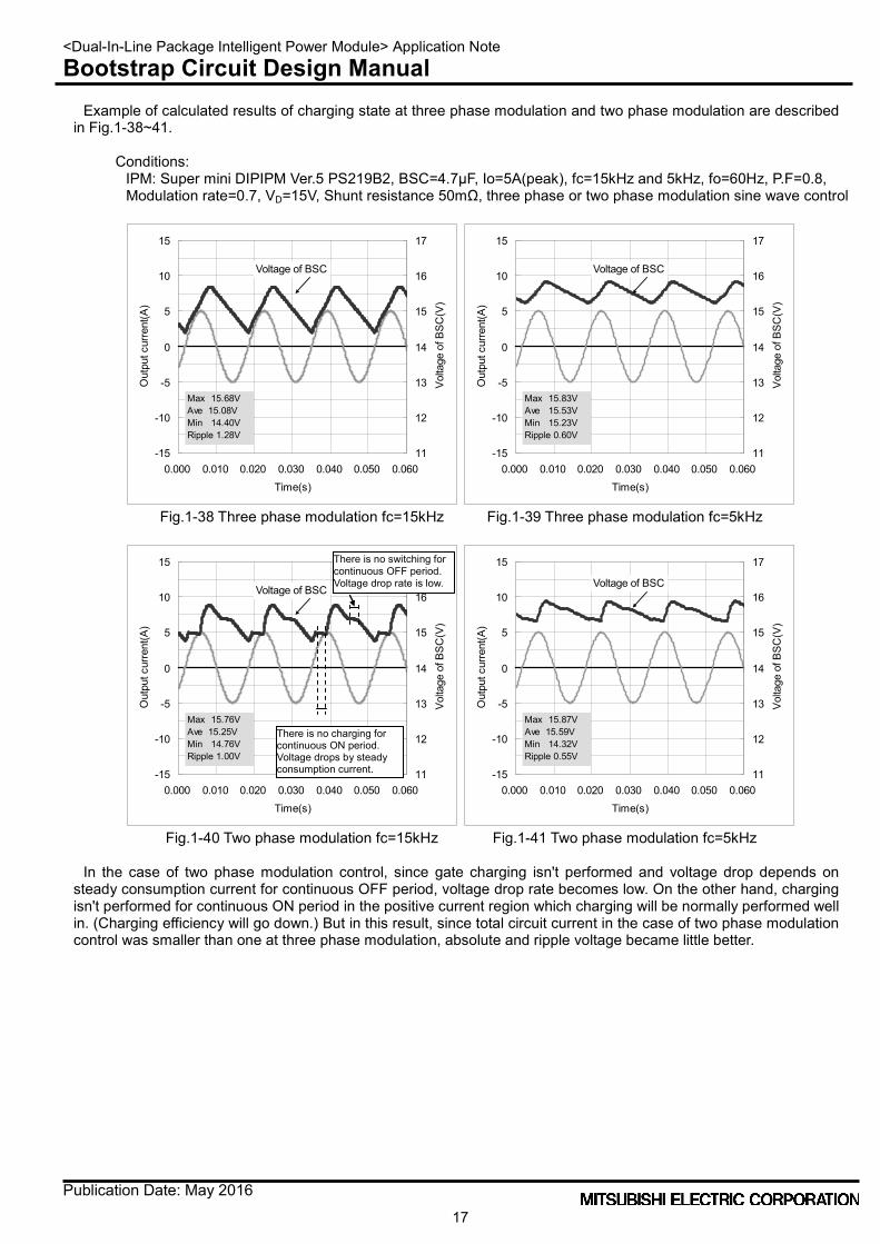
Example of calculated results of charging state at three phase modulation and two phase modulation are described in Fig.1-38~41.
Conditions:
IPM: Super mini DIPIPM Ver.5 PS219B2, BSC=4.7μF, Io=5A(peak), fc=15kHz and 5kHz, fo=60Hz, P.F=0.8, Modulation rate=0.7, VD=15V, Shunt resistance 50mΩ, three phase or two phase modulation sine wave control
Fig.1-38 Three phase modulation fc=15kHz Fig.1-39 Three phase modulation fc=5kHz
Fig.1-40 Two phase modulation fc=15kHz Fig.1-41 Two phase modulation fc=5kHz
In the case of two phase modulation control, since gate charging isn't performed and voltage drop depends on
steady consumption current for continuous OFF period, voltage drop rate becomes low. On the other hand, charging isn't performed for continuous ON period in the positive current region which charging will be normally performed well in. (Charging efficiency will go down.) But in this result, since total circuit current in the case of two phase modulation control was smaller than one at three phase modulation, absolute and ripple voltage became little better.
-15
-10
-5
0
5
10
15
0.000 0.010 0.020 0.030 0.040 0.050 0.060
Time(s)
Out
put c
urre
nt(A
)
11
12
13
14
15
16
17
Vol
tage
of B
SC
(V)
Max 15.68VAve 15.08VMin 14.40VRipple 1.28V
Voltage of BSC
-15
-10
-5
0
5
10
15
0.000 0.010 0.020 0.030 0.040 0.050 0.060
Time(s)O
utpu
t cur
rent
(A)
11
12
13
14
15
16
17
Vol
tage
of B
SC
(V)
Max 15.83VAve 15.53VMin 15.23VRipple 0.60V
Voltage of BSC
-15
-10
-5
0
5
10
15
0.000 0.010 0.020 0.030 0.040 0.050 0.060
Time(s)
Out
put c
urre
nt(A
)
11
12
13
14
15
16
17
Vol
tage
of B
SC
(V)
Max 15.76VAve 15.25VMin 14.76VRipple 1.00V
Voltage of BSC
-15
-10
-5
0
5
10
15
0.000 0.010 0.020 0.030 0.040 0.050 0.060
Time(s)
Out
put c
urre
nt(A
)
11
12
13
14
15
16
17
Vol
tage
of B
SC
(V)
Max 15.87VAve 15.59VMin 14.32VRipple 0.55V
Voltage of BSC
There is no charging for continuous ON period. Voltage drops by steady consumption current.
There is no switching for continuous OFF period. Voltage drop rate is low.

<Dual-In-Line Package Intelligent Power Module> Application Note Bootstrap Circuit Design Manual
Publication Date: May 2016
18
Revision Record
Rev. Date Points
1 10/15/2012 New 2 05/04/2016 Section 1.3.1 Correct some description of mark(e.g. VDB,VBSC and so on,)

<Dual-In-Line Package Intelligent Power Module> Application Note Bootstrap Circuit Design Manual
Publication Date: May 2016
19
© 2016 MITSUBISHI ELECTRIC CORPORATION. ALL RIGHTS RESERVED. DIPIPM and CSTBT are trademarks of MITSUBISHI ELECTRIC CORPORATION.
Keep safety first in your circuit designs!
Mitsubishi Electric Corporation puts the maximum effort into making semiconductor products better and more reliable, but there is always the possibility that trouble may occur with them. Trouble with semiconductors may lead to personal injury, fire or property damage. Remember to give due consideration to safety when making your circuit designs, with appropriate measures such as (i) placement of substitutive, auxiliary circuits, (ii) use of non-flammable material or (iii) prevention against any malfunction or mishap.
Notes regarding these materials
•These materials are intended as a reference to assist our customers in the selection of the Mitsubishi semiconductor product best suited to the customer’s application; they do not convey any license under any intellectual property rights, or any other rights, belonging to Mitsubishi Electric Corporation or a third party.
•Mitsubishi Electric Corporation assumes no responsibility for any damage, or infringement of any third-party’s rights, originating in the use of any product data, diagrams, charts, programs, algorithms, or circuit application examples contained in these materials.
•All information contained in these materials, including product data, diagrams, charts, programs and algorithms represents information on products at the time of publication of these materials, and are subject to change by Mitsubishi Electric Corporation without notice due to product improvements or other reasons. It is therefore recommended that customers contact Mitsubishi Electric Corporation or an authorized Mitsubishi Semiconductor product distributor for the latest product information before purchasing a product listed herein. The information described here may contain technical inaccuracies or typographical errors. Mitsubishi Electric Corporation assumes no responsibility for any damage, liability, or other loss rising from these inaccuracies or errors. Please also pay attention to information published by Mitsubishi Electric Corporation by various means, including the Mitsubishi Semiconductor home page (http://www.MitsubishiElectric.com/).
•When using any or all of the information contained in these materials, including product data, diagrams, charts, programs, and algorithms, please be sure to evaluate all information as a total system before making a final decision on the applicability of the information and products. Mitsubishi Electric Corporation assumes no responsibility for any damage, liability or other loss resulting from the information contained herein.
•Mitsubishi Electric Corporation semiconductors are not designed or manufactured for use in a device or system that is used under circumstances in which human life is potentially at stake. Please contact Mitsubishi Electric Corporation or an authorized Mitsubishi Semiconductor product distributor when considering the use of a product contained herein for any specific purposes, such as apparatus or systems for transportation, vehicular, medical, aerospace, nuclear, or undersea repeater use.
•The prior written approval of Mitsubishi Electric Corporation is necessary to reprint or reproduce in whole or in part these materials.
•If these products or technologies are subject to the Japanese export control restrictions, they must be exported under a license from the Japanese government and cannot be imported into a country other than the approved destination. Any diversion or re-export contrary to the export control laws and regulations of Japan and/or the country of destination is prohibited.
•Please contact Mitsubishi Electric Corporation or an authorized Mitsubishi Semiconductor product distributor for further details on these materials or the products contained therein.