Embed Size (px)
Citation preview

DTIC FILE COPY _ r Form Ag pow d
REPORT DOCUMENTATION PAGE [_ 0M o N0 o7 186
" ratoq i -m m ofk"" O toon 0 URete to ~"@ I ftq m" mm.. the imn e fr 0r emmmq ntmm. uwq ommgmm a do"9atfmtmq .wd rap@ Ue owMNd wememg aim revem thm caiICr"g of awem... SW4u 'OWue a I~uu UNla ow m or oew Wa sown ofmCOIIONO at mmm~ ir iugl. roI Ifmm Iut1ut tmm, tef~.t W ltOA NoS/fln m.. O(w~5t5 1xmml mIeimsga Osmm sew MS.mm 11 Jatm
cc46 Mwin. WW. te Z . m'. tinot OI fVm. "O a mowm bosI. Pumem, SomqeSifeet IO54wfO 2013a.
1. AG.NCY US& ONLY (LOOM,. biah 12. REPORT OATE I3. REPORT TYPE AND DATES COVEREDI 1 30 June 1990 I inal Reroort May 85 - 30 Aor 90n a. TTU AND SUETITI s. FUNOING NUMUERS
4 :rnvesZ!gation ;f a ',Iew Concept in Semiconductor Microwave AFOSR-85-0193
r1 k Osc1lators
.O L AUTHORS)
'ames A. Cooper, jr.
~ 7. PERFORMING ORGANIZATION NAME(S) AND AOORESS(ES) . PERFORMING ORGANIZATION
School of Electrical Enaineering REPORT NUMIER
Purdue University'West Lafayette, IN 47907
3. SPONS04UGI MONITORING AGENCY NAME(S) AND AOORIESS(IS) 10. SPONSORING/IMONIT ORINGAFOSR, NE AGENCY REPORT NUMBER
S3uildinu d10 - ".3d 1 ing AF3, DC 20332-6448 0 L
11. SUPPLEMENTARY NOTES
12a. OISTRUUTION/AVAILASIITY STATEMENT 1ib. DISTRIBUTION COOE
MESFET structure. The resistive gate establishes a uniform electric field in the regime of negativedifferential mobility for electrons in GaAs. At these fields, dipolar charge domains form in thechannel and drift into the drain, producing microwave oscillations in the drain current. In thecontiguous domain mode, a continuous sequence of charge domains forms throughout the channel.This mode is possible because the resistive gate screens the self-induced fields of each dipolardomain, keeping the field outside the domain unperturbed. Frequencies up to 100+ GHz arepreducted, independent of channel length, and the frequency should be tunable over at least oneoctave by varying the gate-to-source voltage. This mode has not yet been observedexperimentally, since the gate resistivity on our prototype devices has been too large. Thesedevices are presently operating in a single domain transit time mode, producing oscillations in the 6to 28 GHz range for channel lengths from 5 to 20 Wm. Work is continuing to reduce the gateresistivity so that the contiguous domain mode can be Observed.
14. SUIUICT TERMS I1141BE OF PAGES
COO, contiguous domain oscillator, RG-MESFET " 18,/ L6. PRICE COO&
1-1 SECURITY CLASSIFICATION I I. SECURITY CLASSIFICATION 19. SECURITY C.ASSIFICATION 2i. uMITATION OF AASTRACT
OF REPORT OF THIS PAGE Off ABSTACT
unclassified unclassified unclassified ULNSN ?S4041-UOSS00 Stancard nom 31 (310104 orfm
W4011111" I

Investigation of a New Concept in
Semiconductor Microwave Oscillators
Final Report
30 June 1990
James A. Cooper, Jr.School of Electrical Engineering
Purdue UniversityWest Lafayette, IN 47907
Introduction and Background
In this program we have investigated a new class of monolithic millimeter waveoscillators. These devices are based on the geometry of a resistive gate metal-semiconductor field effect transistor (RG-MESFET). RG-MESFET oscillatordevices are attractive because they are easily fabricated on standard MESFETprocessing lines and can be easily incorporated into planar monolithic millimeterwave integrated circuits (MMICs).
We initially set out to demonstrate that RG-MESFET devices could be used toform a contiguous sequence of Gunn-like charge domains in the channel, the"contiguous domain mode". Such devices are referred to as contiguous domainoscillators, or "CDOs". In the process of this research, we learned that severaldesign conditions must be met in order that contiguous domains can form, and ifthese conditions are not met, then other oscillation modes are observed instead.The most interesting of these "other" modes is the single-domain transit timemode. It is also possible to fabricate RG-MESFET devices with channel dopingtoo low to allow charge domains to form at all. These devices exhibit a strongstable negative transconductance which might also be used as the basis for amicrowave oscillator.
The contiguous domain oscillator (CDO) is an RG-MESFET in which a sequenceof contiguous dipole domains form spontaneously and continuously in the channelnear the source and propagate along the channel into the drain. This uniquebehavior was first predicted by computer simulations, and arises because of thetwo dimensional nature of the electrostatic boundary conditions in the device.Simulations indicate that the frequency of oscillation is not related to the channellength, but instead is determined by the domain width and the drift velocity. Thedomain width (or spatial period) is inversely proportional to the average electron

density in the channel, a quantity which is controlled by the gate-to-sourcevoltage. Thus it is possible to modulate the frequency during operation byvarying the gate-to-source voltage. Frequencies in the range from a few GHz toover 100 GHz are predicted, independent of channel length.
In this report we will outline the accomplishments of approximately five years ofsponsored research, the first three years under grant no. AFOSR-85-0193 and thelast two years under a continuation grant and no-cost extensions.
Research Objectives
The major objective of this research was to fabricate and characterize resistivegate MESFET oscillators. It was hoped that the contiguous domain mode wouldbe observed. As will be seen, the CDO mode has not yet been realized, but RG-MESFET devices have been operated in the single-domain transit time mode,producing microwave oscillations in the range from 6 to 28 GHz.
Status of the Research
A. Fabrication of Experimental Devices
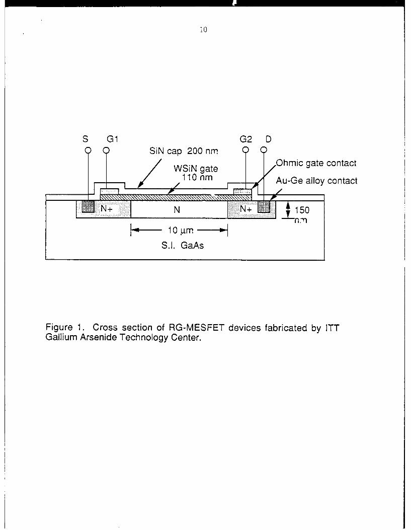
Experimental devices in the form of resistive gate MESFETs were designed atPurdue, and masks were sent to the ITT Gallium Arsenide Technology Center inRoanoke, VA, for fabrication. A cross section of the experimental device isshown in Fig 1. Six wafers containing several thousand devices each were startedin late 1987, and three of the original six were delivered to Purdue on 23February, 1988. The wafers had been fabricated with a range of channel depthsand dopings in an attempt to bracket the optimum design. A summary of the sixwafers is given below, where the asterisk indicates those wafers which actuallycompleted the process and were received at Purdue.
Wafer No. Channel Depth Channel Doping ACC . For [ -,
NTIS CRAMI V1
CDO-1-1 2000 A lx10 17 cm- 3 OTI C Ta,CDO-1-2 2000 A 2x10 17 cm-3 ,.,
CDO-1-3* 2000 A 4x10 17 cm-3 , . -.CDO-1-4* 1500 A 5x10 16 cm-3
CDO-1-5* 1500 A 1x10 17 cm-3 r, 1 ,,CDO-1-6 15oo A 2x10 17 cm-3
Av '1,, / ort,,'i
Dist Av QCOif

3
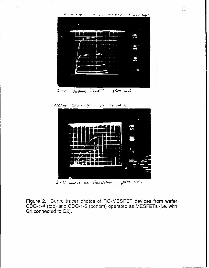
Of the three wafers received at Purdue, CDO-1-3 showed essentially nomodulation of drain current under wide variations in gate bias, probably due tothe high doping level and thick channel. Wafer CDO-1-5 had substantialmodulation, but it's characteristics seemed less ideal than those of CDO-1-4.Examples of I-V curves with the oscillator devices operated as simple MESFETs(VGG=O) are shown in Fig. 2.
Wafer CDO-1-4 was chosen for the initial measurements. It was soon found thatany attempt to operate these devices with a non-zero lateral gate field (i.e.VGG>O) resulted in early device failure. This failure was caused by a designdecision to place the ohmic contact to the resistive gate 5 gm back from the edgesof the source and drain regions, as shown in Fig. 3. At the lateral gate fieldsnecessary for domain formation to occur (E=1 V/gm) the potential of the gate ata point directly over the edge of the drain was about 5 V more negative than thepotential at the ohmic contact. Since the gate-to-drain breakdown voltage wasonly about 4 V, the devices failed due to gate-drain breakdown.
The design oversight was corrected on a portion of wafer CDO-1-4 byreprocessing at Purdue. This consisted of plasma etching the SiN cap layer andevaporating a layer of aluminum to extend each ohmic contact closer to the edgesof the source and drain, as illustrated in Fig. 4. The lithography for theseoperations was done by direct write on wafer using our Cambridge EBMFelectron beam lithography system. Once the modifications had been made, thedevices on CDO-1-4 no longer failed upon application of the gate field, and DCbias could be maintained indefinitely at the level necessary for microwave testing.
B. Microwave Testing of Wafer CDO-1-4
The section of wafer CDO-1-4 which had been modified to have the extendedohmic contacts was sawed into individual chips, each containing eighteen CDOdevices. The test chips were mounted on a TO-5 package and one CDO devicewas wire bonded to the pins of the package, as shown in the upper portion of Fig.5. The TO-5 package was mounted in a waveguide insertion unit as shown in thelower portion of Fig. 5. The insertion unit was WR-28 size, having operatingfrequency range of 26-40 GHz. It was not possible to mount the CDO test chipinto a smaller cavity owing to the dimensions of the test chip, about 2.4 mm perside. The waveguide insertion unit was terminated at one end by a sliding short,and the other end connected through a slide screw tuner to a Tektronixwaveguide mixer. Mixers covering the bands 26-40, 40-60, and 60-90 GHz wereused szquentially. The mixer was connected to a Tektronix 2755 spectrumanalyzer capable of tuning to 325 GHz. Tests were run with a resolutionbandwidth of 1 MHz with a sensitivity of around -50 to -70 dBm.
4
Several devices were tested using the arrangement of Fig. 5. During testing, thebiases to the CDO device were systematically varied, as was the position of thesliding short and the slide-screw tuner. The frequency range from 26 to 90 GHzwas covered with no evidence of oscillation. Subsequent calculations indicatedthat the devices on wafer CDO-1-4 had a channel doping -- channel thicknesssquared (ND tpi2) product which is too low for domain formation to occur.
Wafer CDO-1-5 had a channel doping of l.2x10 17 cm- 3, twice as large as waferCDO-1-4. Repeating the calculation for the devices on wafer CDO-1-5 indicatedthe ND tepi 2 product was large enough to allow domains to form. For this reason,all subsequent investigations were preformed on devices from wafer CDO-1-5.
C. Microwave Testing of Wafer CDO-1-5
Devices from wafer CDO-1-5 were reprocessed at Purdue to reduce the spacingbetween the gate contacts and source/drain edges. These devices were againmounted on TO-5 packages, and initial microwave measurements were conductedin the WR-28 waveguide apparatus of Fig. 5. Microwave signals were observedimmediately upon application of bias to the first device. The signals were in therange from 37 to 42 GHz, and the frequency could be modulated by gate-to-source bias, as shown in Fig. 6. The operation was highly consistent andrepeatable from day to day. Devices could be operated continuously for hours ata time, day after day, with no change in behavior observed.
A number of devices having different width and length were measured, and asummary of their oscillation frequencies is given in Fig. 7. Notice that thefrequencies in Fig. 7 are in the range from 22 to 30 GHz, considerably lowerthan the signals in Fig. 6. After further investigation it became apparent thateach device produced signals in both the 22-30 GHz and 37-42 GHz bandssimultaneously, and that these signals always appeared in the ratio 3:2, suggestingthat both were harmonics of a fundamental signal in the range of 11 to 15 GHz.This fundamental signal could not be observed directly, since the cutofffrequency of the WR-28 waveguide was 21 GHz. In order to verify the existenceof a fundamental signal below 21 GHz, it was necessary to mount the devices on astripline, as shown in Fig. 8. At this point, we began a careful series ofexperiments to measure the oscillation frequency and all four terminal currents(Is, ID, IG1, and IG2) as a function of each of the three terminal voltages (VSG,VGG, and VDG). The results of these measurements are shown in Figs. 9-11.
Figure 9 shows how frequency and terminal currents depend upon source-to-gatevoltage. Note that the frequency ranges from 12.7 to 14.7 GHz as VSG is varied
5
from 5.0 to 6.1 V. Oscillations are not observed for VSG below 4.5 V or above6 V. The dramatic decrease of source current and increase of gate-1 current forVSG greater than 7 V is due to avalanche breakdown of the gate-to-sourcejunction.
Figure 10 shows that both frequency and current are essentially independent ofdrain voltage for VDG less than about 4.5 V. This is evidence that conditions inthe channel are effectively isolated from the drain due to the screening effect cfthe resistive gate. For VDG greater than about 4.5 V, the drain current increasesrapidly and the gate-2 current decreases, indicating avalanche breakdown of thegate-to-drain junction.
Figure 11 shows frequency and power as a function of gate-to-gate voltage. Theoutput power of a 10 gm wide device ranges between 0.1 and 1 tW forfrequencies around 13 GHz. Both the frequencies and the power are much lowerthan expected for the contiguous domain mode. A considerable amount of effortwas expended to make sure no oversights in the theoretical description of thedevice were responsible for the discrepancy. Eventually, the persistentdisagreement with theoretical predictions and the fact that the observedfrequencies were essentially equal to the inverse of the transit time from sourceto drain led us to suspect that these devices were actually operating in a singledomain transit time mode. This was confirmed by measuring frequencies ondevices of different channel length, as shown in Fig. 12.
D. Discussion of Results
The failure of the contiguous domain mode to appear in these devices can betraced to the action of the resistive gate in screening the local fields due to chargedomains in the channel. In order for screening to occur, i.e. in order for the gateto provide a linearly varying potential (constant field), it is necessary that localmotion of image charges on the gate not appreciably disturb the applied DCelectric field. This requires that the gate resistivity be below a critical value. Ifwe require that the local voltage drops on the gate be small compared to theapplied field, we can derive a restriction on the gate resistivity pg,
Pg AQ RMs vd << EA
where Pg is the sheet resistance of the gate, AQRMs the RMS variation of chargedensity in the domain, vd the domain drift velocity, and EA the applied electricalfield. Taking typical values, EA = 8000 V/cm, AQRMS = 7x10⁻⁸ C/cm 2, and Vd =1.3x107 cm/s, then Pg should be much less than 9 k92 per square. The

6
experimental devices on wafer CDO-1-5 has a gate sheet resistance of 30 k 2 persquare.
The effect of too high a gate resistivity is illustrated dramatically in Fig. 13,where we show a computer simulation of a device operating in the contiguousdomain mode. In this calculation, we assume an ideal gate (i.e. a perfectly linearpotential distribution) and calculate the motion of charge domains in the channel.We then assume that on the real gate, image charges would move at the same rateas the charges in the channel in order to provide the necessary screening. Thefigure shows the actual potential variation on the gate at 10 ps intervals for a gateresistivity of 30 kK2 per square. Not only does the potential in the middle of thegate vary with time by almost a factor of two, but at any particular time thepotential as a function of position has an oscillatory behavior which producesalternating regions of positive and negative electric field. This is observed underconditions where a uniform positive electric field is expected and required.Clearly, the violent perturbation of gate potential would have dire consequencesfor the formation and behavior of domains in the channel. To illustrate the roleof gate resistivity in this situation, we show in Fig. 14 the gate potential for thesame operating conditions if the gate resistivity were reduced to 3 kf2 per square.With this lower gate resistivity, the linear potential along the gate is virtuallyundisturbed by the motion of image charges.
E. Work Presently Underway
In order to reduce the resistivity of the gates in our experimental devices, wehave developed a procedure for electron beam evaporation of mixed powers ofCr and SiO to form a "cermet" resistive film. In this procedure, the original gateis first removed by plasma etching to expose bare GaAs. The maskingphotoresist is left on the wafer, and approximately 3000 A of 55% Cr / 45% SiOweight mixture is evaporated. The cermet film is patterned by liftoff, and asecond lithography step is performed by direct electron beam exposure to definegate contacts. A Ti/Au layer is then evaporated and patterned by liftoff. Finally,a thermal annealing step is required to produce low contact resistance. Thisannealing step also reduces the gate resistivity in a manner which is predictablebased on the temperature and duration of the anneal. It is necessary to take thisreduction into account when depositing the original cermet film.
The development of this process has taken considerable effort, since fairly lowresistivity is required with low contact resistance and good repeatability. We arenow ready to apply this procedure to modify devices on wafer CDO-1-5. Wehave found experimentally that the 3 k92 cermet film can be biased to therequired voltage under DC conditions without bum-out due to heating.
7
F. Summary
At this point in the program, at the end of Air Force funding, we have not yetreached our goal of demonstrating the contiguous domain mode of operation.We have, however, observed oscillations in the single domain transit time mode,with fundamental frequencies ranging from 6 to 28 GHz as channel length isvaried from 20 gm to 6 ptm. This mode of operation in a resistive gate MESFETis absolutely unique and is clearly distinct from a lateral Gunn diode. The obviousdifference is that the driving field is derived from the resistive gate, and hencethe oscillation conditions are independent of and isolated from the drain voltage.
At this point we have every reason to believe that the contiguous domain modewill be obtained in the near future. Clearly, the high value of gate resistance inour present devices would prevent the gate from approximating the ideal linearpotential needed for contiguous domain formation. We expect that our efforts toreduce the gate resistance in these devices will be successful, and we hope toobserve frequencies in the 60-90 GHz range on the modified devices.

8
Publications
[1] Y. Yin, J. A. Cooper, Jr., P. G. Neudeck, M. L. Balzan, and A. E.Geissberger. "Negative Transconductance in a Resistive Gate MESFET",submitted to Appl. Phys. Lett.. January, 1989.
[2] Y. Yin, J. A. Cooper, Jr., P. G. Neudeck, M. L. Balzan. and A. E.Geissberger, "Room Temperature Negative Transconductance in aResistive Gate GaAs FET", WOCSEMMAD, Hilton Head, SC, February20-22, 1989.
[31 J. A. Cooper, Jr., Y. Yin, M. L. Balzan, and A. E. Geissberger,"Microwave Characterization of the Contiguous Domain Oscillator," IEEEDevice Research Conference, Cambridge, MA, June 19-21, 1989.
[4] J. A. Cooper, Jr., Y. Yin, M. L. Balzan, and A. E. Geissberger,"Experimental Verification of the Contiguous Domain Oscillator Concept,"12th IEEE/Cornell Conference on Advanced Concepts in High SpeedSemiconductor Devices and Circuits, Ithaca, NY, August 7-9, 1989.
[5] J. A. Cooper, Jr., Y. Yin, M. L. Balzan, and A. E. Geissberger,"Microwave Characterization of a Resistive-Gate MESFET Oscillator,"IEEE Electron Device Lett. Vol. 10, pp. 493-495, November, 1989.
[6] Y. Yin, H. J. Fu, J. A. Cooper, Jr., M. L. Balzan, and A. E. Geissberger,"Operation of a Resistive Gate MESFET in the Single Domain TransitTime Mode," submitted to IEEE Electron Device Lett.
Technical Reports
[1] J. S. Kleine and J. A. Cooper, Jr., "Rapid Thermal Annealing of SiliconImplanted Gallium Arsenide", School of Electrical Engineering, PurdueUniversity, TR-EE 86-43, December, 1986.
[2] Y. Yin, J. A. Cooper, Jr., and H. Fu, "Investigation of a Resistive-GateMESFET Contiguous Domain Oscillator", School of ElectricalEngineering, Purdue University, TR-EE 90-25, April, 1990.
9
Professional Personnel
Principal investigator:
James A. Cooper, Jr. , Professor of Electrical Engineering
Graduate research assistants:
Ming Fang, MS 1985Thesis title: "Fabrication and Characterization of Thin Metal Films"
John S. Kleine, MS 1986Thesis title: "Rapid Thermal Annealing of Silicon Implanted GalliumArsenide"
Robert E. Beaty, Ph.D 1988Thesis title: "A Bias Tunable Monolithic Microwave Oscillator -- TheContiguous Domain Oscillator"
Yiwen Yin, Ph.D 1990.Thesis title: "Investigation of the MESFET Version Contiguous DomainOscillator"
Hua Julia Fu, Ph.D in progress
Industrial Interactions
We have received substantial support from the ITT Gallium Arsenide TechnologyCenter, Roanoke, VA, in th, form of device fabrication and consulting onmicrowave testing. Industrial interest has also been expressed by the Magnavoxgovernment systems division in Ft. Wayne, IN, and by the Magnavox GaAs groupin Torrance, CA.
iO
S G1 G2 DSiN cap 200 nm
Ohmic gate contact7L110 nmAu-Ge alloy contact
H- 10urn - H n
S.i. GaAs
Figure 1. Cross section of RG-MESFET devices fabricated by ITTGallium Arsenide Technology Center.
t11
*UEE-;E2Ex
MEN PAP"UurN--....MaESENMs
Figure 2. Curve tracer photos of RG-MESFET devices from wafer000-1-4 (top) and CDO-1 -5 (bottom) operated as MESFETs (i.e. withGi connected to 02).

12
S G1 G2 D
...... .....
10 4m
S.I. GaAs
Figure 3: Cross section of RG-MESFET devices showing typicaldimensions. The 5 gm separation between gate contact the the edgeof the source/drain junctions lead to undesirable voltage drop alongthe portion of the resistive gate over the source and drain.
S Gi G2 D0.5 gm 0.5 Lm
N+ N-N
~~10 m-,
S.I. GaAs
Figure 4. Cross section of the experimental CDO device after the gate ohmiccontacts had been modified at Purdue. The structure shown above cansustain continuous DC biasing at fields high enough to allow domain formation.

13
TE l10
CDOTest Chip TO-5 Package
Slide-ScrewTuner
t ~Device _7
SlidingShort WR-28
Waveguide
Insertion Unit Mixer
Figure 5. Top View: Cross section of mounting arrangement with the drain wire of the CDOdevice connected through a slot in the top of the waveguide, serving as an E-field antenna.Bottom View: Cross section of entire waveguide apparatus, including sliding short andslide-screw tuner.

-60 . ...... ..
V =16VGG
;-65
0 -70 ... .. .i.......
5.35 VVSG= 5.0 V 5.5 VSG5.2 V 5.7 V
-75 .....
37 38 39 40
Frequency (GHz)
Figure 6. Power spectra for the first observed microwave oscillation fromwafer CDO-1 -5. The figure shows a series of spectra obtained at differentvalues of source-to-gate bias.
30 _ _ _
U. U-- i° Oo r n on
CDOA
>1 25 Li A__ _ _ _ _ _ _
LL A tiD AC0A 1 CDO3 CDO7
1 CDo4 0 CDO820 1 - , .I • I , , '
0.0 0.5 1.0 1.5 2.0
Vsg (V)
Figure 7. Oscillation frequency of several CDO devices from waferCDO-1 -5 as a function of source-to-gate voltage. The gate field is8000 V/cm. Channel width and length are: CDO 1', 2, and 3 (10x10lam), CDO 4 (10x20 m), CDO 5 (20x10 lam), CDO 6 (20x20 gim),CDO 7 (10x50 lam), CDO 8 (200x10 lam).

15
CDO device stripline
to bias tee
~and
analyzer
Figure 8: Stripline mounting arrangement for CDO testing. Bias issupplied via pins on the TO-5 can, while the microwave signal is taken outvia the stripline to the spectrum analyzer. A bias tee is inserted betweenthe stripline and the spectrum analyzer (not shown) to bias the drain.

16
4 L . 15IF I s 0
3 S
DN2 14
E G2
G1 -40" -i 0)
0 13 0.
- LL-1 K--
-2 123 4 5 6 7 8
VSG (V)
Figure 9. Frequency and terminal currents as a function of source-to-gate voltage with gate field constant at 8000 V/cm. Drain-to-gatevoltage is zero.
5 14f
//o/ D 7
N
13 "E 3s
222 GI 12
1 LI.
G 2
0 I I I 11
-2 0 2 4 6 8 10VD4 (V)
Figure 10. Frequency and terminal currents as a function of drain-to-gate voltage with gate field constant at 8000 V/cm. Source-to-gatevoltage is held at 5.5 V.

17
15 '20
-.3014 E
.7 -40 m
Cr r 0
LL -60
NF
14 15 16 17 18 19
V G (V)
Figure 11. Frequency and microwave power as a function of gate-to-gate voltage. Source-to-gate voltage is 5.5 V and drain-to-gate voltageis zero.
30 . . . . i . . .
U0C/
25 .
-6
N 20
S15
LL 5
0 j, , I . . i , , i . .
14 1.5 16 17 018 192
1/L (1/gm)
Figure 12. Frequency versus reciprocal channel length for four CDOdevices from wafer CD0-1 -5. The linear dependence indicates thatthe devices are operating in the single domain transit time mode.

18
28-0c. -89
-s 10 s itr"
0 1 20 30
Po iti on (urn)
Figure 13. Potential of resistive gate versus position at 10 ps intervalsduring operation assuming that charges move in the channel as thoughthe gate were ideal. Gate resistivity is 30 kQ per square. Note that thegate potential is significantly perturbed by the motion of image charges.
28-Oct-89
15
(Y) 10
1-*
= 5
0o 20 60 30
Position (um)
Figure 14. Potential of resistive gate for the same conditions as Fig 13,except that the gate sheet resistance is reduced to 3 kW per square. Atthis value of gate resistivity, the potential is virtually undisturbed by themotion of image charges.