Embed Size (px)
Citation preview
2003 Microchip Technology Inc. DS70096A
dsPICDEM™
MC1H 3-Phase
High Voltage Power Module
User’s Guide
Note the following details of the code protection feature on Microchip devices:
• Microchip products meet the specification contained in their particular Microchip Data Sheet.
• Microchip believes that its family of products is one of the most secure families of its kind on the market today, when used in the
intended manner and under normal conditions.
• There are dishonest and possibly illegal methods used to breach the code protection feature. All of these methods, to our
knowledge, require using the Microchip products in a manner outside the operating specifications contained in Microchip's Data
Sheets. Most likely, the person doing so is engaged in theft of intellectual property.
• Microchip is willing to work with the customer who is concerned about the integrity of their code.
• Neither Microchip nor any other semiconductor manufacturer can guarantee the security of their code. Code protection does not
mean that we are guaranteeing the product as “unbreakable.”
Code protection is constantly evolving. We at Microchip are committed to continuously improving the code protection features of our
products. Attempts to break microchip’s code protection feature may be a violation of the Digital Millennium Copyright Act. If such acts
allow unauthorized access to your software or other copyrighted work, you may have a right to sue for relief under that Act.
Information contained in this publication regarding device
applications and the like is intended through suggestion only
and may be superseded by updates. It is your responsibility to
ensure that your application meets with your specifications.
No representation or warranty is given and no liability is
assumed by Microchip Technology Incorporated with respect
to the accuracy or use of such information, or infringement of
patents or other intellectual property rights arising from such
use or otherwise. Use of Microchip’s products as critical
components in life support systems is not authorized except
with express written approval by Microchip. No licenses are
conveyed, implicitly or otherwise, under any intellectual
property rights.
DS70096A-page ii
Trademarks
The Microchip name and logo, the Microchip logo, dsPIC,
KEELOQ, MPLAB, PIC, PICmicro, PICSTART, PRO MATE and
PowerSmart are registered trademarks of Microchip
Technology Incorporated in the U.S.A. and other countries.
FilterLab, microID, MXDEV, MXLAB, PICMASTER, SEEVAL
and The Embedded Control Solutions Company are
registered trademarks of Microchip Technology Incorporated
in the U.S.A.
Accuron, Application Maestro, dsPICDEM, dsPICDEM.net,
ECONOMONITOR, FanSense, FlexROM, fuzzyLAB, In-
Circuit Serial Programming, ICSP, ICEPIC, microPort,
Migratable Memory, MPASM, MPLIB, MPLINK, MPSIM,
PICC, PICkit, PICDEM, PICDEM.net, PowerCal, PowerInfo,
PowerMate, PowerTool, rfLAB, rfPIC, Select Mode,
SmartSensor, SmartShunt, SmartTel and Total Endurance are
trademarks of Microchip Technology Incorporated in the
U.S.A. and other countries.
Serialized Quick Turn Programming (SQTP) is a service mark
of Microchip Technology Incorporated in the U.S.A.
All other trademarks mentioned herein are property of their
respective companies.
© 2003, Microchip Technology Incorporated, Printed in the
U.S.A., All Rights Reserved.
Printed on recycled paper.
2003 Microchip Technology Inc.
Microchip received QS-9000 quality system certification for its worldwide headquarters, design and wafer fabrication facilities in Chandler and Tempe, Arizona in July 1999 and Mountain View, California in March 2002. The Company’s quality system processes and procedures are QS-9000 compliant for its PICmicro® 8-bit MCUs, KEELOQ® code hopping devices, Serial EEPROMs, microperipherals, non-volatile memory and analog products. In addition, Microchip’s quality system for the design and manufacture of development systems is ISO 9001 certified.
dsPICDEM™ MC1H 3-PHASE
HIGH VOLTAGE POWER MODULE
Safety Notice
The safety notices and operating instructions provided should be adhered to, to
avoid a safety hazard. If in any doubt, consult your supplier.
WARNING – This system must be earthed (grounded) at all times.
CAUTION – The system should not be installed, operated, serviced or modified
except by qualified personnel who understand the danger of electric shock
hazards and have read and understood the user instructions. Any service or
modification performed by the user is done at the user’s own risk and voids all
warranties.
WARNING – The output terminals are NOT isolated from the incoming AC mains
supply and may be at up to 410V with respect to ground, regardless of the input
mains supply voltage applied. These terminals are live during operation AND for
3 minutes after disconnection from the supply. Do not attempt to access the
terminals or remove the cover during this time. Note that this same shock hazard
applies to any external brake resistor connected, which will also be live, and
therefore protection equivalent to double insulation should be provided.
WARNING – The unit may obtain power through the output terminals if these are
connected to a rotating motor acting as a generator. If this is the case, then the
previous warning also applies (i.e., the output terminals are live when connected
to the generator and for 3 minutes after the generator has been stopped). Note
that this case can arise even when the unit has been disconnected from the
incoming AC mains supply.
CAUTION – If a motor is connected to the output of this unit, the frame should be
connected to the output protective ground terminal provided. Particular care
should be taken to mechanically guard such a motor, bearing in mind that
unexpected behavior is likely to result from the process of code development.
CAUTION – For continued protection against the risk of fire, replace the fuse with
one of the same type only (i.e., T5A H 250V, Time Lag 5A High Breaking Capacity
250V minimum).
© 2003 Microchip Technology Inc. DS70096A-page iii

dsPICDEM™ MC1H 3-Phase High Voltage Power Module
• The system is intended for evaluation and development purposes and
should only be operated in a normal laboratory environment as defined by
IEC 61010-1:2001.
• Clean with a dry cloth only.
• Operate flat on a bench, do not move during operation and do not block the
ventilation holes.
• The system should not be operated without all the supplied covers fully
secured in place.
• Screws should not protrude into the unit by more than 5 mm (0.2″), type M3
ISO metric.
• The system should not be connected or operated if there is any apparent
damage to the unit.
• The unit is designed for installation category II and to be connected to the
AC mains supply via a standard non-locking plug. As the unit has no mains
switch, this plug constitutes the means of disconnection from the supply
and thus the user must have unobstructed access to this plug during
operation.
DS70096A-page iv © 2003 Microchip Technology Inc.
2003 Microchip Technology Inc. DS70096A-page v
dsPICDEM™ MC1H 3-PHASE
HIGH VOLTAGE POWER MODULE
Table of Contents
Safety Notice ............................................................................................................................ iii
Preface........................................................................................................................................ 1
Chapter 1. Set Up and Operation
1.1 Introduction ................................................................................................................... 5
1.2 Using The Motor Control 3-Phase High Power Module ................................................ 7
1.3 Current and Power Limitations.................................................................................... 14
1.4 Detailed Description of Operation ............................................................................... 17
1.5 Modifying The Board ................................................................................................... 30
1.6 Test Points .................................................................................................................. 36
1.7 User Signal Connector Pinout (37-Pin, D-Type) ......................................................... 37
Appendix A: Circuit Diagrams ........................................................................................... 39
Appendix B: Source Code................................................................................................... 47
Worldwide Sales and Service.............................................................................................. 54

dsPICDEM™ MC1H 3-Phase High Voltage Power Module
NOTES:
DS70096A-page vi © 2003 Microchip Technology Inc.
dsPICDEM™ MC1H 3-PHASE
HIGH VOLTAGE POWER MODULE
Preface
This chapter contains general information about this manual and contacting customer
support.
HIGHLIGHTS
Topics covered in this chapter:
• About this Guide
• Warranty Registration
• Recommended Reading
• The Microchip Web Site
• Development Systems Customer Notification Service
• Customer Support
ABOUT THIS GUIDE
Document Layout
This document describes how to use the Microchip dsPICDEM™ MC1H High Voltage
3-Phase Power Module. The manual layout is as follows:
• Chapter 1: Set Up and Operation – Describes what the product is, what makes it
a desirable development tool, how to install it and the basic features of the
interface.
• Worldwide Sales and Service – Lists Microchip sales and service locations and
telephone numbers worldwide.
Documentation Updates
All documentation becomes dated and this user’s guide is no exception. Since
MPLAB® IDE, MPLAB C1X and other Microchip tools are constantly evolving to meet
customer needs, some actual dialogs and/or tool descriptions may differ from those in
this document. Please refer to our web site to obtain the latest documentation available.
Documentation Numbering Conventions
Documents are numbered with a “DS” number. The number is located on the bottom of
each page, in front of the page number. The numbering convention for the DS Number
is: DSXXXXXA,
where:
XXXXX = The document number.
A = The revision level of the document.
© 2003 Microchip Technology Inc. DS70096A-page 1

dsPICDEM™ MC1H 3-Phase High Voltage Power Module
WARRANTY REGISTRATION
Please complete the enclosed Warranty Registration Card and mail it promptly.
Sending in your Warranty Registration Card entitles you to receive new product
updates. Interim software releases are available at the Microchip web site.
RECOMMENDED READING
This user’s guide describes how to use the dsPICDEM MC1H 3-Phase High Voltage
Power Module. The data sheets contain current information on programming the
specific microcontroller devices.
THE MICROCHIP WEB SITE
Microchip provides online support on the Microchip World Wide Web (WWW) site. The
web site is used by Microchip as a means to make files and information easily available
to customers. To view the site, you must have access to the Internet and a web browser
such as Netscape Navigator® or Microsoft® Internet Explorer.
The Microchip web site is available by using your favorite Internet browser to attach to:
http://www.microchip.com
The web site provides a variety of services. Users may download files for the latest
development tools, data sheets, application notes, user's guides, articles and sample
programs. A variety of information specific to the business of Microchip is also
available, including listings of Microchip sales offices, distributors and factory
representatives.
Technical Support
• Frequently Asked Questions (FAQ)
• Online Discussion Groups - Conferences for products, Development Systems,
technical information and more
• Microchip Consultant Program Member Listing
• Links to other useful web sites related to Microchip products
Engineer's Toolbox
• Design Tips
• Device Errata
Other available information
• Latest Microchip Press Releases
• Listing of seminars and events
• Job Postings
DS70096A-page 2 © 2003 Microchip Technology Inc.

Preface
DEVELOPMENT SYSTEMS CUSTOMER NOTIFICATION SERVICE
Microchip started the customer notification service to help our customers keep current
on Microchip products with the least amount of effort. Once you subscribe, you will
receive e-mail notification whenever we change, update, revise or have errata related
to your specified product family or development tool.
Go to the Microchip web site at (http://www.microchip.com) and click on Customer
Change Notification. Follow the instructions to register.
The Development Systems product group categories are:
• Compilers
• Emulators
• In-Circuit Debuggers
• MPLAB® Development Systems
• Programmers
Here is a description of these categories:
Compilers – The latest information on Microchip C compilers and other language
tools. These include the MPLAB C17, MPLAB C18 and MPLAB C30 C compilers;
MPASM™ and MPLAB ASM30 assemblers; MPLINK™ and MPLAB LINK30 object
linkers; MPLIB™ and MPLAB LIB30 object librarians.
Emulators – The latest information on Microchip in-circuit emulators. This includes the
MPLAB® ICE 2000 and MPLAB® ICE 4000.
In-Circuit Debuggers – The latest information on Microchip in-circuit debuggers.
These include the MPLAB® ICD and MPLAB ICD 2.
MPLAB Development Systems – The latest information on Microchip MPLAB® IDE,
the Windows® Integrated Development Environment for development systems tools.
This list is focused on the MPLAB® IDE, MPLAB SIM and MPLAB SIM30 simulators,
MPLAB IDE Project
Manager and general editing and debugging features.
Programmers – The latest information on Microchip device programmers. These
include the PRO MATE® II device programmer and PICSTART® Plus development
programmer.
© 2003 Microchip Technology Inc. DS70096A-page 3

dsPICDEM™ MC1H 3-Phase High Voltage Power Module
CUSTOMER SUPPORT
Users of Microchip products can receive assistance through several channels:
• Distributor or Representative
• Local Sales Office
• Field Application Engineer (FAE)
• Corporate Applications Engineer (CAE)
• Hotline
Customers should call their distributor, representative or field application engineer
(FAE) for support. Local sales offices are also available to help customers. See the
back cover for a list of sales offices and locations.
Corporate Applications Engineers (CAEs) may be contacted at (480) 792-7627.
In addition, there is a Systems Information and Upgrade Line. This line provides system
users a list of the latest versions of all of Microchip's development systems software
products. Plus, this line provides information on how customers can receive any
currently available upgrade kits.
The Hotline Numbers are:
1-800-755-2345 for U.S. and most of Canada.
1-480-792-7302 for the rest of the world.
DS70096A-page 4 © 2003 Microchip Technology Inc.
dsPICDEM™ MC1H 3-PHASE
HIGH VOLTAGE POWER MODULE
Chapter 1. Set Up and Operation
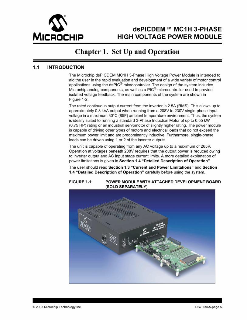
1.1 INTRODUCTION
The Microchip dsPICDEM MC1H 3-Phase High Voltage Power Module is intended to
aid the user in the rapid evaluation and development of a wide variety of motor control
applications using the dsPIC® microcontroller. The design of the system includes
Microchip analog components, as well as a PIC® microcontroller used to provide
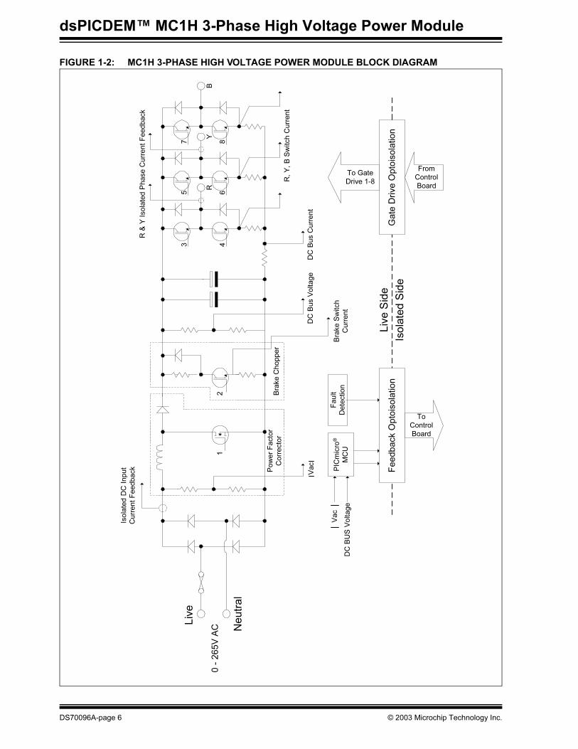
isolated voltage feedback. The main components of the system are shown in
Figure 1-2.
The rated continuous output current from the inverter is 2.5A (RMS). This allows up to
approximately 0.8 kVA output when running from a 208V to 230V single-phase input
voltage in a maximum 30°C (85F) ambient temperature environment. Thus, the system
is ideally suited to running a standard 3-Phase Induction Motor of up to 0.55 kW
(0.75 HP) rating or an industrial servomotor of slightly higher rating. The power module
is capable of driving other types of motors and electrical loads that do not exceed the
maximum power limit and are predominantly inductive. Furthermore, single-phase
loads can be driven using 1 or 2 of the inverter outputs.
The unit is capable of operating from any AC voltage up to a maximum of 265V.
Operation at voltages beneath 208V requires that the output power is reduced owing
to inverter output and AC input stage current limits. A more detailed explanation of
power limitations is given in Section 1.4 “Detailed Description of Operation”.
The user should read Section 1.3 “Current and Power Limitations” and Section
1.4 “Detailed Description of Operation” carefully before using the system.
FIGURE 1-1: POWER MODULE WITH ATTACHED DEVELOPMENT BOARD
(SOLD SEPARATELY)
© 2003 Microchip Technology Inc. DS70096A-page 5
dsPICDEM™ MC1H 3-Phase High Voltage Power Module
FIGURE 1-2: MC1H 3-PHASE HIGH VOLTAGE POWER MODULE BLOCK DIAGRAM
PIC
mic
ro®
MC
U
DC
Bus V
oltage
DC
Bus C
urr
ent
Bra
ke C
hopper
R
R,
Y,
B S
witch C
urr
ent
Liv
e
Ne
utr
al
0 -
265V
AC
Pow
er
Facto
r
Corr
ecto
r
Isola
ted D
C I
nput
Curr
ent
Feedback
YB
R &
Y I
sola
ted P
hase C
urr
ent
Feedback
3 4
5 6
7 81
2
Vac
Feedback O
pto
isola
tion
Fault
Dete
ction
Vac
DC
BU
S V
oltage
Gate
Dri
ve O
pto
isola
tion
Liv
e S
ide
Iso
late
d S
ide
Bra
ke S
witch
Curr
ent
To
Control
Board
From
Control
Board
To Gate
Drive 1-8
DS70096A-page 6 © 2003 Microchip Technology Inc.
Set Up and Operation
1.2 USING THE MOTOR CONTROL 3-PHASE HIGH POWER MODULE
1.2.1 Introduction
The user should be aware of the operating procedures outlined below and ensure that
they are followed. Failure to do so may result in damage to the system.
1.2.2 Making Power Connections
It is recommended that cables be terminated with blue or red insulated crimp
terminals. If crimp terminals are not used, care should be taken to ensure that stray
strands of wire do not short to adjacent terminals or the enclosure. If possible, all
wires should be stripped and tinned with solder before connecting to the power
module terminals.
For the AC mains supply input, standard double-insulated, 3-core flex cable should be
used with a minimum current rating of 10A (1 mm2 18 AWG). A computer power cable
can be used when the IEC connector is removed.
The recommended output cable size is 1.0 to 1.5 mm2 (18-16 AWG) and it should
have a 600V rating. This cable should also be double insulated or have a protective
ground screen.
Access to the terminal screws is provided via holes in the lid of the enclosure. A flat
blade screwdriver should be used.
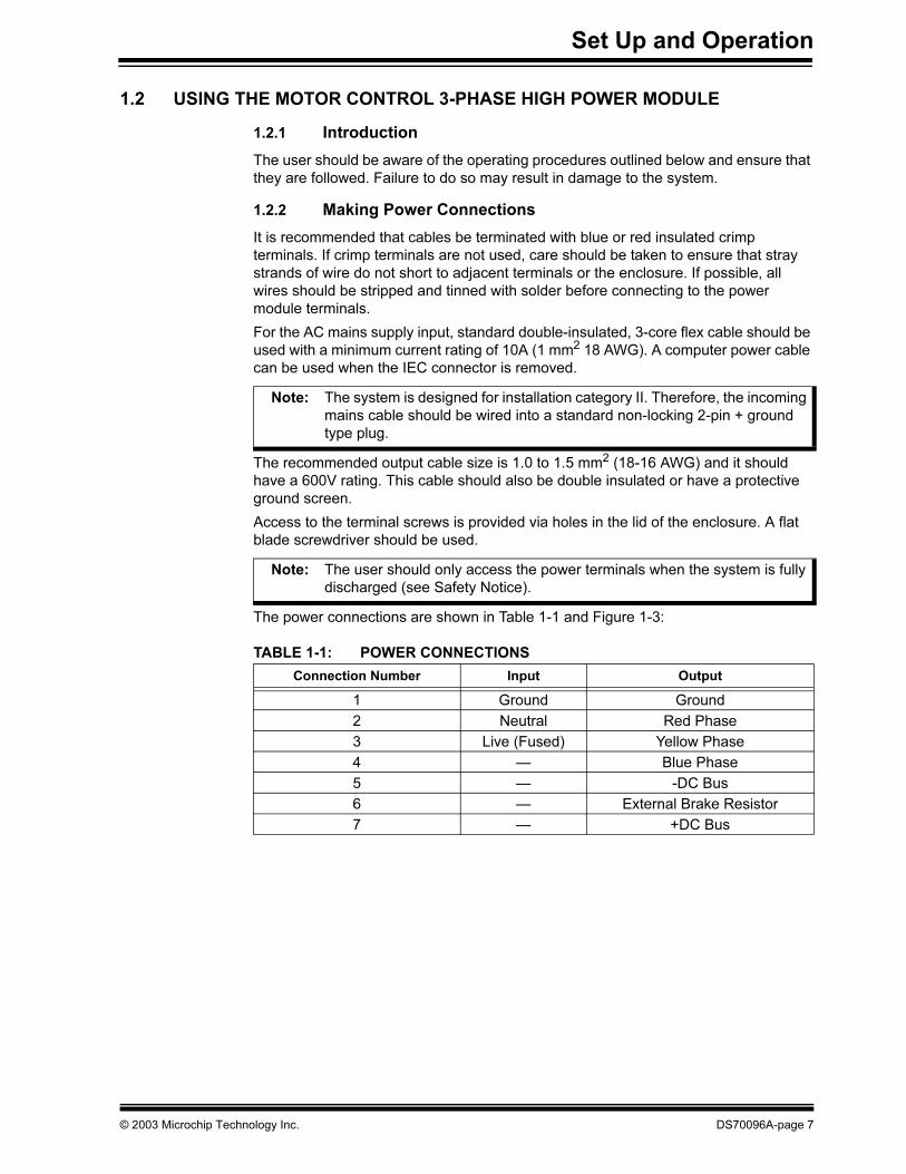
The power connections are shown in Table 1-1 and Figure 1-3:
TABLE 1-1: POWER CONNECTIONS
Note: The system is designed for installation category II. Therefore, the incoming
mains cable should be wired into a standard non-locking 2-pin + ground
type plug.
Note: The user should only access the power terminals when the system is fully
discharged (see Safety Notice).
Connection Number Input Output
1 Ground Ground
2 Neutral Red Phase
3 Live (Fused) Yellow Phase
4 — Blue Phase
5 — -DC Bus
6 — External Brake Resistor
7 — +DC Bus
© 2003 Microchip Technology Inc. DS70096A-page 7
dsPICDEM™ MC1H 3-Phase High Voltage Power Module
FIGURE 1-3: POWER CONNECTIONS
Using output connections 6 and 7, the user may connect an external braking resistor.
The user should consider the maximum and average power to be dissipated at the
required DC bus voltage when considering the resistor value. They should also
consider the peak allowable resistor current of 4A. For example, if regulating at 400V
then a 100Ω minimum value should be used which would allow 1.6 kW (at most) to be
dissipated.
The user may feed in an external DC supply using output connections 5 and 7. This
offers the simplest way for a user to bypass the PFC section of the unit. In the simplest
case all the user needs to do is use an external rectifier and fuse. The input current
rating when using the auxiliary DC input is 15A (RMS). The inverter output rating is
unchanged. Note that if using the auxiliary DC input, the internal fuse, soft-start, PFC
and ground FAULT protection is bypassed. It is up to the user to ensure adequate
external protection circuitry is used and incoming DC voltage is correctly regulated.
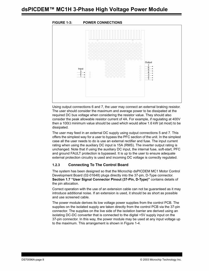
1.2.3 Connecting To The Control Board
The system has been designed so that the Microchip dsPICDEM MC1 Motor Control
Development Board (02-01648) plugs directly into the 37-pin, D-Type connector.
Section 1.7 “User Signal Connector Pinout (37-Pin, D-Type)” contains details of
the pin allocation.
Correct operation with the use of an extension cable can not be guaranteed as it may
introduce additional noise. If an extension is used, it should be as short as possible
and use screened cable.
The power module derives its low voltage power supplies from the control PCB. The
supplies on the isolated supply are taken directly from the control PCB via the 37-pin
connector. The supplies on the live side of the isolation barrier are derived using an
isolating DC-DC converter that is connected to the digital +5V supply input on the
37-pin connector. In this way, the power module may be used at any input voltage up
to the maximum. This arrangement is shown in Figure 1-4.
7654321
321
Input
Output
DS70096A-page 8 © 2003 Microchip Technology Inc.
Set Up and Operation
FIGURE 1-4: POWER ELECTRONICS GATE DRIVE STAGES
Note that the incoming digital 0V from the development board is grounded within the
power module (as shown in Figure 1-4) to ensure user safety. When a PC or any other
device is connected to the control board there is therefore the possibility of a “ground
loop” occurring. If this is suspected, the user should first try to eliminate the stray
magnetic field causing the problem by relocating the offending transformer or by using
shielding. If this is not possible, then the equipment connected to the development
board should be isolated from the digital 0V.
Position and speed feedback transducers are connected to the control board directly
and not via the power module. No electrical isolation is provided on the control board
for these signals and so the transducers must be isolated.
Consult the development board documentation for details of signal interfacing and
how to connect in-circuit emulators and debugging equipment.
POWER ELECTRONICS GATE DRIVE
STAGES
ISOLATED
HALL-EFFECT
CURRENT
TRANSDUCERS
CONDITIONING
OF LIVE
FEEDBACK
SIGNALS
FAULT
DETECTION
AND LATCHING
CIRCUITRY
OPTOCOUPLERS
5V LINEAR
REGULATOR
INCOMING GROUND
CONNECTED TO
CHASSIS
+15V
OU
T
LIVE
ISOLATED
ISOLATING
DC : DC
CONVERTER
Pin
27
Pin
9
Pin
18
&36
Pin
19
&37
9V Power
Supply Input
(Floating)
Rectify
Smooth and
Regulate
Digital +5V
Digital 0V
To Digital
Circuits
To Analog
Circuits
Analo
g +
5V
Analo
g 0
V
Control PCB 02-01648
Power PCB 02-01647
© 2003 Microchip Technology Inc. DS70096A-page 9

dsPICDEM™ MC1H 3-Phase High Voltage Power Module
1.2.4 Power-Up/Power-Down Sequence
The user should ensure that the following sequence are followed.
1.2.4.1 POWER-UP SEQUENCE
• With the development board plugged in, turn on the power supply feeding the
control PCB (if not already on).
• One or more of the fault lights may illuminate. This is normal.
• Turn on the AC supply to the power module.
• Reset the system by activating the active high ISO_RESET line. The ISO_RESET
line is on pin 33 of the 37-pin, D-type (see Section 1.7 “User Signal Connector
Pinout (37-Pin, D-Type)”). If using the dsPICDEM MC1 Motor Control
Development Board, this signal is routed to pin 14 of the 30F6010 dsPIC device,
which is on Port RE9. The minimum pulse width for the RESET is 2 µs. The
RESET should be done in coordination with the SPI™ handling routine of the
dsPIC device to ensure correct synchronization of the serial interface providing
the isolated voltage feedback (see Section 1.2.6.2 “Isolated Feedback” and
Section 1.4.7.2 “Isolated Voltage Feedback”). The system is now ready to use.
1.2.4.2 POWER-DOWN SEQUENCE
• Stop firing all power devices.
• Turn off the incoming AC supply.
• Wait until the red DC bus LED indicator visible through the ventilation holes in the
top of the unit has gone out (this will take 3 minutes or less).
• Turn off the power supply feeding the control card (if required).
1.2.5 Power Device Switching Frequencies
The PFC stage has been designed for a switching frequency of 50 kHz (±5%).
This offers a good system compromise between cost, size and efficiency. The
modulation frequency affects not only the losses in the power switches and diode but
also that in the PFC inductor and snubbing components. The user should not deviate
from the stated carrier frequency. The user should note that a typical regulation level
for the DC bus is between 350-400V.
If the user does not wish to use the PFC stage the PFC switches can simply be
left off. However, the PFC inductor and diode will be left in circuit and the input
current will remain limited to 5A (RMS) and 8.9A Peak. The user should read Section
1.5.3.3 “Bypassing The PFC” if this is unacceptable.
The Brake chopper switch has been designed so that it may be switched up to a
maximum frequency of 16 kHz. This frequency limit is chosen for power dissipation
and low voltage power supply consumption reasons. In most braking applications a
lower modulation frequency will be used, as there is little benefit (apart from acoustic
noise) from modulating at such a high frequency.
The six inverter switches have been designed so that they may be switched up
to a maximum frequency of 20 kHz. This frequency limit is chosen for power
dissipation and low voltage power supply consumption reasons. Unless extremely low
output current harmonics or very high bandwidth control is required, it is suggested
that a 16 kHz carrier frequency be used. This offers lower loss while still being
inaudible. It also has the advantage that the dead time insertion will cause less
distortion of the output voltage.
DS70096A-page 10 © 2003 Microchip Technology Inc.
Set Up and Operation
Given the high side and low side switches of the inverter are connected in series
across the DC bus (see Figure 2.1), both switches should never be turned on at the
same time. Turning both switches on effectively places a short circuit across the DC
bus and is called “Shoot Through”. Shoot Through should be avoided at all costs. In
order to avoid Shoot Through, an appropriate time delay must be inserted between
the turn off command to one device and the turn on command to the other device of
the same inverter leg. This time is called the “Dead Time”. The required Dead Time
depends on the switching speeds of the power devices and the timing delays due to
the optocouplers and the gate drive circuits.
Writing to the appropriate registers in the dsPIC device (DTCON1 and DTCON2) sets
the dead time. Refer to the dsPIC30F Family Reference Manual (DS70046) for details.
Although not necessary for correct operation of the system, it is common practice to
eliminate very narrow firing commands. This is because they will have negligible effect
on the output waveform but incur additional switching loss. It is suggested that a duty
cycle that gives transistor on or off times of less than 100 ns be eliminated by rounding
the duty cycle up or down as appropriate. Note that pulses, which are narrower than
the dead time set in the Motor Control PWM Module, are automatically eliminated.
In order to provide an economic design, so-called bootstrap power supplies are used
for the high side inverter switches (see Section 1.4.3.3 “Gate Drive” for details). As
the charging path for these is only made when the corresponding low side switch or
diode conducts, this places some minor restrictions on modulation. These are as
follows:
1. When the power module is first energized after a period of time where no
modulation has taken place, all low side switches should be turned on for 2-3 µs.
This ensures the bootstrap supplies are “primed”. This can be simply done by
using the output override facility in the dsPIC Motor Control PWM module by
setting the correct bits in the OVDCON register. Care should be taken to ensure
a shoot through does not accidentally occur. The possibility of a shoot through
fault will be minimized if the dsPIC PWM module is operated in the
complementary Output mode (module default).
2. If the user is continuously modulating all the low side switches as part of their
PWM strategy, the “priming” step is not strictly necessary, as it will happen
automatically. There will however be a delay of variable duration before the high
side switches actually fire. The delay will depend on the particular operating
circumstances and whether it is acceptable or not will depend on the particular
application.
3. In extreme circumstances, it is possible that the high side bootstrap supply will
discharge while the system is running. This will not happen for typical sinusoidal
modulation schemes provided an inductive load (e.g., a motor) is connected. If a
bootstrap supply collapses, an under-voltage lockout will automatically occur to
protect the high side switch entering the linear region of operation. The high side
switch is turned off whatever the command. The lockout is automatically cleared
when the bootstrap supply is restored and the next turn-on edge occurs. If
necessary, the user should periodically apply a refresh pulse to the low side
switch in a similar manner to that described for priming above.
Note: No hardware Dead Time is included in the design as it is included as a
feature of the Motor Control PWM Module of the dsPIC device. A minimum
Dead Time of 2 µs should be used. This applies to both turn on and turn off
of both devices.
Note: The user should verify that all PWM frequencies and dead time settings are
correct using an oscilloscope before connecting the control signals to the
power module.
© 2003 Microchip Technology Inc. DS70096A-page 11
dsPICDEM™ MC1H 3-Phase High Voltage Power Module
1.2.6 Power Module Feedback Signals
1.2.6.1 INTRODUCTION
The power module may be operated in two distinct ways with respect to signal
isolation. This effects which of the feedback signals are available. All feedback signals
are preconditioned and scaled within the power module. Which particular set of
feedback signals the user requires will change depending on the application. Typically
industrial applications tend to use isolated signals for both safety, noise and
performance reasons. More cost-sensitive applications, and especially those that
have little or no user input, tend to run the control electronics live and use non-isolated
feedback signals.
1.2.6.2 ISOLATED FEEDBACK
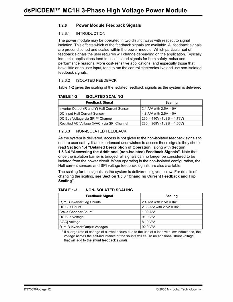
Table 1-2 gives the scaling of the isolated feedback signals as the system is delivered.
TABLE 1-2: ISOLATED SCALING
1.2.6.3 NON-ISOLATED FEEDBACK
As the system is delivered, access is not given to the non-isolated feedback signals to
ensure user safety. If an experienced user wishes to access these signals they should
read Section 1.4 “Detailed Description of Operation” along with Section
1.5.3.4 “Accessing the Additional (non-isolated) Feedback Signals”. Note that
once the isolation barrier is bridged, all signals can no longer be considered to be
isolated from the power circuit. When operating in the non-isolated configuration, the
Hall current sensors and SPI voltage feedback signals are also available.
The scaling for the signals as the system is delivered is given below. For details of
changing the scaling, see Section 1.5.3 “Changing Current Feedback and Trip
Scaling”.
TABLE 1-3: NON-ISOLATED SCALING
Feedback Signal Scaling
Inverter Output (R and Y) Hall Current Sensor 2.4 A/V with 2.5V = 0A
DC Input Hall Current Sensor 4.8 A/V with 2.5V = 0A
DC Bus Voltage via SPI™ Channel 230 = 410V (1LSB = 1.78V)
Rectified AC Voltage (|VAC|) via SPI Channel 230 = 369V (1LSB = 1.60V)
Feedback Signal Scaling
R, Y, B Inverter Leg Shunts 2.4 A/V with 2.5V = 0A*
DC Bus Shunt 2.38 A/V with 2.5V = 0A*
Brake Chopper Shunt 1.09 A/V
DC Bus Voltage 91.0 V/V
|VAC| Voltage 81.9 V/V
R. Y, B Inverter Output Voltages 92.0 V/V
* If a large rate of change of current occurs due to the use of a load with low inductance, the
voltage across the self-inductance of the shunts will cause an additional shunt voltage
that will add to the shunt feedback signals.
DS70096A-page 12 © 2003 Microchip Technology Inc.
Set Up and Operation
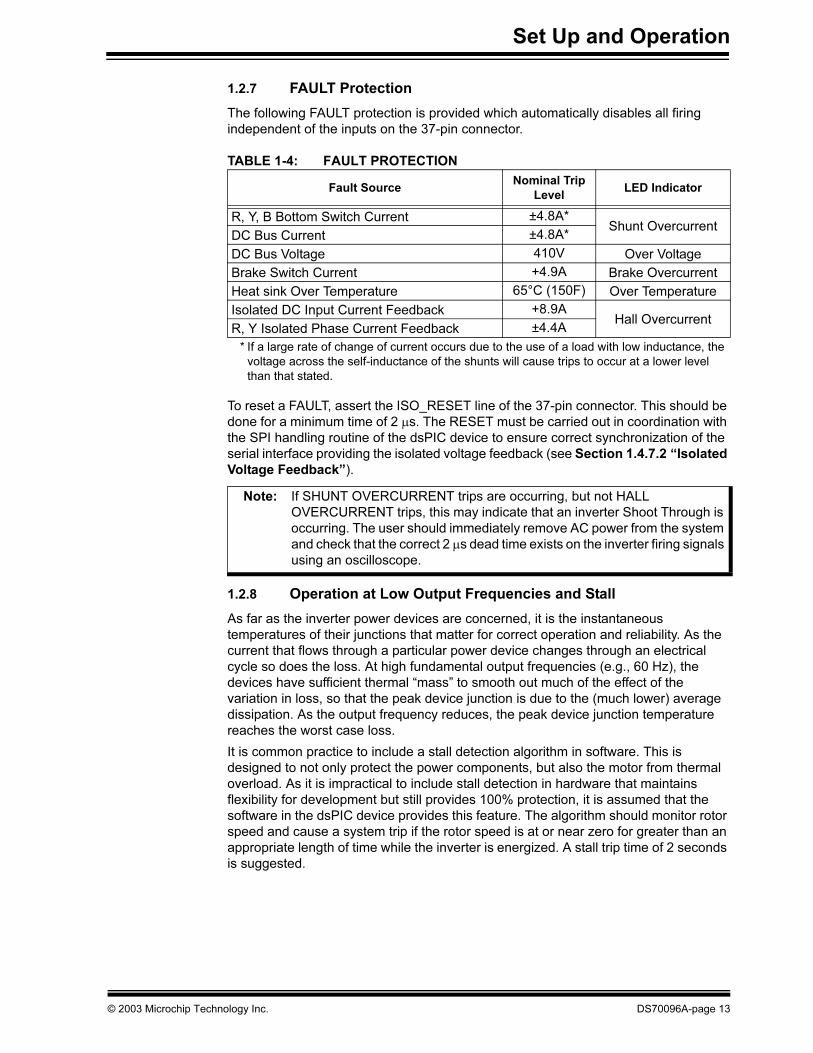
1.2.7 FAULT Protection
The following FAULT protection is provided which automatically disables all firing
independent of the inputs on the 37-pin connector.
TABLE 1-4: FAULT PROTECTION
To reset a FAULT, assert the ISO_RESET line of the 37-pin connector. This should be
done for a minimum time of 2 µs. The RESET must be carried out in coordination with
the SPI handling routine of the dsPIC device to ensure correct synchronization of the
serial interface providing the isolated voltage feedback (see Section 1.4.7.2 “Isolated
Voltage Feedback”).
1.2.8 Operation at Low Output Frequencies and Stall
As far as the inverter power devices are concerned, it is the instantaneous
temperatures of their junctions that matter for correct operation and reliability. As the
current that flows through a particular power device changes through an electrical
cycle so does the loss. At high fundamental output frequencies (e.g., 60 Hz), the
devices have sufficient thermal “mass” to smooth out much of the effect of the
variation in loss, so that the peak device junction is due to the (much lower) average
dissipation. As the output frequency reduces, the peak device junction temperature
reaches the worst case loss.
It is common practice to include a stall detection algorithm in software. This is
designed to not only protect the power components, but also the motor from thermal
overload. As it is impractical to include stall detection in hardware that maintains
flexibility for development but still provides 100% protection, it is assumed that the
software in the dsPIC device provides this feature. The algorithm should monitor rotor
speed and cause a system trip if the rotor speed is at or near zero for greater than an
appropriate length of time while the inverter is energized. A stall trip time of 2 seconds
is suggested.
Fault SourceNominal Trip
LevelLED Indicator
R, Y, B Bottom Switch Current ±4.8A*Shunt Overcurrent
DC Bus Current ±4.8A*
DC Bus Voltage 410V Over Voltage
Brake Switch Current +4.9A Brake Overcurrent
Heat sink Over Temperature 65°C (150F) Over Temperature
Isolated DC Input Current Feedback +8.9AHall Overcurrent
R, Y Isolated Phase Current Feedback ±4.4A
* If a large rate of change of current occurs due to the use of a load with low inductance, the
voltage across the self-inductance of the shunts will cause trips to occur at a lower level
than that stated.
Note: If SHUNT OVERCURRENT trips are occurring, but not HALL
OVERCURRENT trips, this may indicate that an inverter Shoot Through is
occurring. The user should immediately remove AC power from the system
and check that the correct 2 µs dead time exists on the inverter firing signals
using an oscilloscope.
© 2003 Microchip Technology Inc. DS70096A-page 13
dsPICDEM™ MC1H 3-Phase High Voltage Power Module
1.2.9 Field Weakening
If the user is operating a brushless permanent magnet motor using field weakening by
employing phase advance, great care should be taken. If a FAULT trip occurs, firing
will stop, and the full back EMF magnitude, due to the motor's speed, will be present
on the output terminals. Should the peak of the back EMF be above the DC bus,
sudden uncontrolled motor braking will occur. The DC bus will rise in an uncontrolled
manner possibly causing damage to both power devices and the DC bus capacitors. A
speed greater than that which would produce a peak back EMF of greater than 450V,
with no field weakening, should not be used. This should adequately protect the unit. If
using the auxiliary DC input, the user should check the rating of the power supply and
adjust this speed accordingly or use a series blocking diode of suitable rating.
The same care should be taken with separately excited brushed DC motors if
employing field weakening at high speed. If the field current were to be increased in
error, a similar braking phenomenon may occur if the back EMF rises above the DC
bus. The effect is likely to be less severe as a DC over-voltage will occur tripping out
both the armature and field supply (assuming the field is not supplied separately). For
this reason, if using a separately excited DC motor it is recommended that both the
field and the armature are supplied from the unit.
1.3 CURRENT AND POWER LIMITATIONS
The maximum power and current capability of the system is dictated by the allowable
temperature rise of the different components. Establishing maximum limits is not
simple given the host of different ways the user may use the system. The voltage and
the nature of the electrical load used both affects the dissipation that occurs. In
determining the allowable limits for the power semiconductors, the following
assumptions have been made:
• Heat sink is at 70°C (worst case over temperature trip point)
• Thermal resistance of the insulating thermal pad is 4°C/W
Note that the maximum power of the system will always be the lower value due to the
AC input stage or the inverter output stage.
1.3.1 Inverter Output Current Limits
The inverter is capable of providing the full rated output of 2.5 A (RMS) within the
entire operating range (voltage, temperature and at up to 20 kHz PWM carrier
frequency) of the system. This includes being continuously stalled at such an
electrical angle that one of the motor phases is at the peak of the rated output (3.5A)
at just less than 100% duty cycle. This is a condition that causes high thermal loading
because one of the inverter switches has the peak worst case conduction and
switching loss continuously. Note that as far as the power devices are concerned,
operation at output frequencies of less than approximately 10 Hz are equivalent to
stall as far as peak device temperature is concerned because of low thermal
capacitance.
In a practical application, this condition of low output frequency/stall and high duty
cycle is unlikely to happen. With a motor correctly matched to the DC bus voltage, the
switch duty cycle at stall will be approximately 50% thus significantly reducing the
conduction loss in a particular switch. The complementary diode of the inverter phase
will also conduct for approximately 50% thus spreading the conduction loss between
two different power device packages. This in turn leads to a substantial reduction in
device temperature.
DS70096A-page 14 © 2003 Microchip Technology Inc.
Set Up and Operation
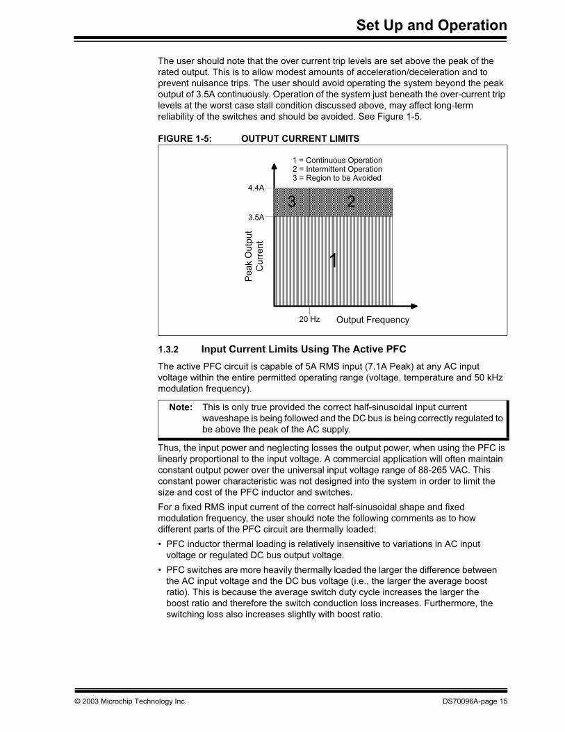
The user should note that the over current trip levels are set above the peak of the
rated output. This is to allow modest amounts of acceleration/deceleration and to
prevent nuisance trips. The user should avoid operating the system beyond the peak
output of 3.5A continuously. Operation of the system just beneath the over-current trip
levels at the worst case stall condition discussed above, may affect long-term
reliability of the switches and should be avoided. See Figure 1-5.
FIGURE 1-5: OUTPUT CURRENT LIMITS
1.3.2 Input Current Limits Using The Active PFC
The active PFC circuit is capable of 5A RMS input (7.1A Peak) at any AC input
voltage within the entire permitted operating range (voltage, temperature and 50 kHz
modulation frequency).
Thus, the input power and neglecting losses the output power, when using the PFC is
linearly proportional to the input voltage. A commercial application will often maintain
constant output power over the universal input voltage range of 88-265 VAC. This
constant power characteristic was not designed into the system in order to limit the
size and cost of the PFC inductor and switches.
For a fixed RMS input current of the correct half-sinusoidal shape and fixed
modulation frequency, the user should note the following comments as to how
different parts of the PFC circuit are thermally loaded:
• PFC inductor thermal loading is relatively insensitive to variations in AC input
voltage or regulated DC bus output voltage.
• PFC switches are more heavily thermally loaded the larger the difference between
the AC input voltage and the DC bus voltage (i.e., the larger the average boost
ratio). This is because the average switch duty cycle increases the larger the
boost ratio and therefore the switch conduction loss increases. Furthermore, the
switching loss also increases slightly with boost ratio.
3.5A
4.4A
1
Output Frequency
Pe
ak O
utp
ut
Cu
rre
nt
2
20 Hz
1 = Continuous Operation2 = Intermittent Operation
3
3 = Region to be Avoided
Note: This is only true provided the correct half-sinusoidal input current
waveshape is being followed and the DC bus is being correctly regulated to
be above the peak of the AC supply.
© 2003 Microchip Technology Inc. DS70096A-page 15
dsPICDEM™ MC1H 3-Phase High Voltage Power Module
• For a fixed DC bus voltage, the PFC diode is more heavily thermally loaded the
higher the AC input voltage. This is simply due to the increase in power through-
put with higher AC input voltage due to the fixed input current. For a given AC
input voltage operation at lower DC bus voltage will also load the diode more
heavily thermally as the average current increases for the constant power
throughput.
1.3.3 Input Current Limits when Not Using the Active PFC
If the user does not wish to use the PFC stage, the PFC switch can simply be left off.
However the PFC inductor and diode will be left in circuit and the input current will
remain limited to 5A (RMS) and 8.9A Peak to protect the diode. The user will also
notice a large droop with increasing load when the PFC inductor is left in circuit.
Section 1.5.3.3 “Bypassing The PFC” explains how to modify the unit to bypass the
PFC diode or the whole PFC stage.
With the PFC diode removed from the circuit, the rated current increases to 6A (RMS)
limited by the loss in the PFC inductor. With the PFC inductor also removed from the
circuit the rated current increases to 7A (RMS) limited by the NTC soft-start thermistor
and the diode bridge. Note that with the PFC inductor removed from the circuit it is
possible that less input power will be possible despite the higher permitted input
current. This is for two reasons. Firstly because the power factor will be lower without
the PFC inductor to smooth the input current. Secondly, the DC input over-current
protection will be more easily tripped by the surge of current that occurs on initial
conduction of the Diode Bridge.
1.3.4 DC Bus Voltage Ripple
The unit has been designed with 3 x 330 µF DC bus capacitors in parallel thus giving
approximately 1 mF of capacitance. This value is substantially more than a fitting to a
commercial drive of this rating, when running off single-phase 208V AC or higher
when using the PFC. Given the development nature of the system, the capacitance
was oversized to assist those users wishing to use the system without the PFC or at
lower voltages. Figure 1-6 gives the peak-peak DC bus voltage ripple for three
different conditions.
Note: The over current trip levels are set above the peak of the rated output. This
is to allow for current ripple, modest amounts of acceleration and to prevent
nuisance trips. The user should avoid operating the system beyond the
peak rated output of 7.1A RMS continuously or controlling the input
waveshape to be anything other than the correct half-sinusoid. Operation
of the system just beneath the over-current trip levels may affect long-term
reliability of the switches and should be avoided.
DS70096A-page 16 © 2003 Microchip Technology Inc.
Set Up and Operation
FIGURE 1-6: DC BUS VOLTAGE RIPPLE
Note that if operating without the PFC inductor in circuit that the DC bus voltage ripple
is similar in magnitude to that shown above but the average DC bus voltage is higher
for the same power.
1.3.5 Brake Chopper Output Current Limits
The brake chopper switch and diode are capable of providing the full rated output of
4A within the entire operating range (voltage, temperature and at up to 16 kHz
modulation frequency) of the system. The brake chopper diode has been oversized
from that usually required due to the inductance of an external braking resistor and
cables so that the brake chopper is more general purpose.
1.4 DETAILED DESCRIPTION OF OPERATION
1.4.1 AC Supply Input Stage (Appendix A, Sheet 1)
The AC supply input stage of the board consists of the following components:
• F1 – 1.25" x 0.25" 5A 250 VAC high rupture fuse – Note: only replace with part of
the same rating.
• C8 – X2 class film capacitor to aid in the suppression of AC supply transients.
• R11 – A 1W high voltage resistor which acts to discharge C8.
• C9, C10 – Y class film capacitors to aid in the suppression of AC supply transients
and to also provide a low impedance return path for any currents that flows from
the power device tabs to the heat sink and enclosure due to capacitive coupling.
• BR1 – A single-phase bridge rectifier to convert the incoming AC into DC suitable
for input to the power conditioning stage.
• V1 – A metal oxide varistor located across the incoming supply lines to suppress
high energy transients.
0
5
10
15
20
25
30
0 200 400 600 800 1000
Output Power (Watts)P
k-P
k R
ipp
le (
Vo
lts)
PFC Active 208V AC
50 Hz Input 350V Bus
PFC Choke in Circuit
208V AC 50Hz
PFC Choke in Circuit
110V AC 60Hz
Note: The user should note that the over current trip levels are set above the peak
of the rated output. This is to prevent nuisance trips. The user should avoid
operating the system beyond the peak output of 4A continuously. Operation
of the system just beneath the over-current trip of 4.9A may affect long-term
reliability of the brake chopper switch and should be avoided. The value of
the brake chopper resistor should be chosen to ensure no more than 4A
can flow, even at the peak DC bus voltage.
© 2003 Microchip Technology Inc. DS70096A-page 17
dsPICDEM™ MC1H 3-Phase High Voltage Power Module
1.4.2 Input Power Stage (Appendix A, Sheet 1)
1.4.2.1 SOFT-START PROTECTION
• NTC1 – A resistor with a negative temperature coefficient that acts to limit the
surge of input current that would occur at initial application of power due to the
discharged DC bus capacitance. The initial nominal cold resistance is 5W, which
reduces once current flows and the device heats up. Note that when the Power
Factor Correction inductance (L1 and L2) is in circuit that the NTC also reduces
the overshoot in DC bus voltage that other wise occurs on application of power.
1.4.2.2 ACTIVE POWER FACTOR CORRECTION (PFC)
The active PFC circuit is essentially a simple boost chopper with the control aimed at
shaping the input current to follow the incoming mains supply waveshape. The reader
is directed towards a good textbook (e.g., Power Electronics, Mohan et. al. ISBN
0-471-58408-8 pp488-494) for a detailed description of operation and control of the
circuit. The purpose of the different parts of the circuit are described below:
• L1 – A high frequency axial inductor with a single layer winding on a ferrite core.
This component is in series with the main inductor (L2) to reduce the effect of the
self-capacitance of it's winding. Without L1, significant high frequency (15 MHz)
ringing of the inductor current occurs at every transistor turn-on, which would
increase EMI and the PFC transistor switching loss.
• L2 – A power inductor with two stacked toroidal cores made from a powdered-iron
material to limit the core loss while maintaining good energy storage density. The
particular cores used are Micrometals T200-34. A simple multilayer winding is
used which results in moderate copper loss but significant self-capacitance. 142
turns of 1.12 mm diameter enameled copper wire is used. The design offers a
good compromise between cost, core loss and size for this application. The
nominal inductance is 1.15 mH at 5A.
• Q1, Q2 – Two 500V TO220 MOSFETs connected in parallel. As the tabs of the
devices are not isolated, a thermally conductive insulator is used. When closed,
Q1 and Q2 increase the energy stored in the inductor L2. When open, energy
stored in the inductance is transferred to the DC bus capacitors (C3-C5). Energy
is also drawn from the AC supply during this time. By appropriate control of the
switches, the input current wave-shape can be profiled to obtain good power
factor and low harmonic distortion.
• D1 – A 600V DO-220 diode optimized for use at high switching frequency. As the
tab of the device is not isolated, a thermally conductive insulator is used.
• C1, R1, R2 – A “snubber” that acts to damp high frequency oscillations and limit
the rate of change of voltage across Q1 and Q2.
• C3, C4, C5 – 450V 330 mF electrolytic capacitors which act as the main DC bus
energy storage capacitors.
• C2, C6, C7 – 400V 1mF film capacitors which act to source the high frequency
component of current for the PFC stage. Note that the faces of these components
are not insulated.
• U19 – Microchip TC1412N gate drive IC. This contains a low resistance
complementary push-pull MOSFET pair and input circuitry suitable for interfacing
to a wide range of input voltages. It is an ideal choice for this application allowing
up to 2A of peak gate drive current to switch Q1 and Q2 rapidly and therefore
achieve low switching loss. It also has a small footprint allowing it to be located
physically close to the transistors allowing a low inductance gate circuit layout.
DS70096A-page 18 © 2003 Microchip Technology Inc.
Set Up and Operation
• C20, C21, Q11, R45, R46, R52 – These components act to provide a dynamic
level shifting circuit to U19 while Q1 and Q2 switch. Inductance of the power
tracking between the sources of Q1 and Q2 due to the physical board layout
means there is a substantial transient voltage (up to 5V in this case) between the
+15V supply * point reference at R61 and the sources of Q1 and Q2. This simple
low cost circuit allows the power supply of U19 to move transiently. Q11 provides
a level shift to ensure correct assertion of the firing command. In applications with
fewer constraints on physical layout and/or lower switching speed requirements,
these components may not be needed.
1.4.3 Phase Inverter (Appendix A, Sheet 2)
1.4.3.1 INTRODUCTION
The 3-phase inverter has three identical circuits, shown as R (RED) Y (YELLOW) and
B (BLUE). These are often referred to as inverter “legs”. They invert the DC bus back
to a variable AC output waveform by appropriate modulation of the switches. When a
star or delta connected three-phase motor is used, the electrical symmetry can be
exploited to provide bi-directional current and voltage with just three such legs. In this
way, both motoring and generating/braking operation can be used in either direction of
rotation, commonly called “4 Quadrant” control.
There is no reason why the user can not use two of the legs in an “H-bridge”
configuration for control of DC motors or other single-phase applications requiring
bi-directional current and voltage. Even a single leg could be used with just the low
side switch controlled for a simple unidirectional current application (e.g., field control
of a separately excited DC motor).
The detailed description of one “leg” (red phase) is given below. The other legs are
identical in function.
1.4.3.2 POWER DEVICES
• Q3, Q4 – 600V N-Channel IGBT transistors with co-packaged anti-parallel 600V
diodes. They are packaged in the industry standard TO220. As the tabs of the
devices are not isolated, a thermally conductive insulator is used.
• The IGBTs are optimized for switching at frequencies up to 20 kHz while having
improved tolerance to FAULT conditions (at the slight expense of conduction
loss).
• The diodes are of the “soft-recovery” type for reduced RF emissions.
• The tracking between the devices and to the DC bus is designed to minimize the
inductance that causes transient over/undershoots.
• R4 – A 3W 25 mΩ shunt resistor through which the low side switch and diode
returns to the -DC bus. The shunt is used for FAULT protection and (optionally) for
an alternative feedback signal – see Section 1.2.6 “Power Module Feedback
Signals” and Section 1.2.7 “FAULT Protection”.
1.4.3.3 GATE DRIVE
• U22 – An integrated high voltage IC (IR 2112) which provides gate control of a low
side and a high side power transistor. As the emitter of the high side device (Q3)
can be at any potential between -DC and +DC, and even beyond transiently,
internal circuitry must provide for the necessary level shifting to ensure correct
operation. The IR2112 does this without providing isolation. The 2112 also
monitors the low and high side power supplies and shuts down if an under voltage
is detected. The under-voltage lockout is automatically reset by a rising edge of a
firing command once a valid voltage is present. See www.irf.com for a full data
sheet.
© 2003 Microchip Technology Inc. DS70096A-page 19
dsPICDEM™ MC1H 3-Phase High Voltage Power Module
The function of groups of the discrete gate-drive components is explained below:
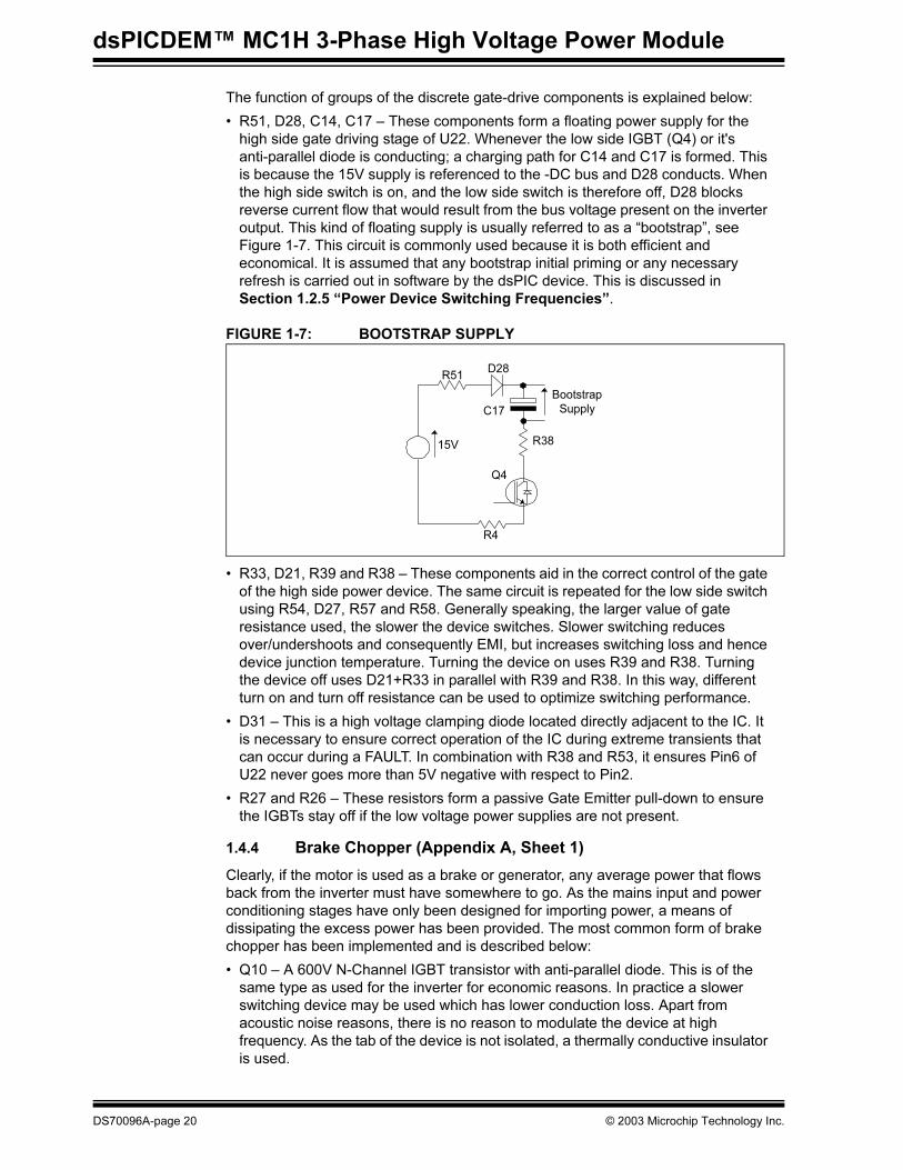
• R51, D28, C14, C17 – These components form a floating power supply for the
high side gate driving stage of U22. Whenever the low side IGBT (Q4) or it's
anti-parallel diode is conducting; a charging path for C14 and C17 is formed. This
is because the 15V supply is referenced to the -DC bus and D28 conducts. When
the high side switch is on, and the low side switch is therefore off, D28 blocks
reverse current flow that would result from the bus voltage present on the inverter
output. This kind of floating supply is usually referred to as a “bootstrap”, see
Figure 1-7. This circuit is commonly used because it is both efficient and
economical. It is assumed that any bootstrap initial priming or any necessary
refresh is carried out in software by the dsPIC device. This is discussed in
Section 1.2.5 “Power Device Switching Frequencies”.
FIGURE 1-7: BOOTSTRAP SUPPLY
• R33, D21, R39 and R38 – These components aid in the correct control of the gate
of the high side power device. The same circuit is repeated for the low side switch
using R54, D27, R57 and R58. Generally speaking, the larger value of gate
resistance used, the slower the device switches. Slower switching reduces
over/undershoots and consequently EMI, but increases switching loss and hence
device junction temperature. Turning the device on uses R39 and R38. Turning
the device off uses D21+R33 in parallel with R39 and R38. In this way, different
turn on and turn off resistance can be used to optimize switching performance.
• D31 – This is a high voltage clamping diode located directly adjacent to the IC. It
is necessary to ensure correct operation of the IC during extreme transients that
can occur during a FAULT. In combination with R38 and R53, it ensures Pin6 of
U22 never goes more than 5V negative with respect to Pin2.
• R27 and R26 – These resistors form a passive Gate Emitter pull-down to ensure
the IGBTs stay off if the low voltage power supplies are not present.
1.4.4 Brake Chopper (Appendix A, Sheet 1)
Clearly, if the motor is used as a brake or generator, any average power that flows
back from the inverter must have somewhere to go. As the mains input and power
conditioning stages have only been designed for importing power, a means of
dissipating the excess power has been provided. The most common form of brake
chopper has been implemented and is described below:
• Q10 – A 600V N-Channel IGBT transistor with anti-parallel diode. This is of the
same type as used for the inverter for economic reasons. In practice a slower
switching device may be used which has lower conduction loss. Apart from
acoustic noise reasons, there is no reason to modulate the device at high
frequency. As the tab of the device is not isolated, a thermally conductive insulator
is used.
15V
Bootstrap
Supply
R51D28
C17
R38
Q4
R4
DS70096A-page 20 © 2003 Microchip Technology Inc.
Set Up and Operation
• D3 – A 8A 600V diode required to freewheel the current around the resistor due to
it's inductance. As the tab of the device is not isolated, a 3W 25mΩ shunt resistor
through which the low side switch and diode returns to the -DC bus. The shunt is
used for FAULT protection and (optionally) for an alternative feedback signal, see
Section 1.4.6 “Shunt Feedback (Appendix A, Sheet 3)” and Section
1.5.3.4 “Accessing the Additional (non-isolated) Feedback Signals”.
• U23 – Microchip TC1412N gate drive IC. This contains a low resistance
complementary push-pull MOSFET pair and input circuitry suitable for interfacing
to a wide range of input voltages. It has a small footprint allowing it to be located
physically close to the transistor, allowing a low inductance gate circuit layout.
Note that the full current drive capability of the TC1412N is not necessarily
required, as high frequency modulation is not essential for a brake chopper. A less
expensive TC1410N or TC1411N could be used.
• R60, R62, R67, Q12, C24, C28 – These components act to provide a dynamic
level shifting circuit to U23 while Q10 switches. Inductance of the power tracking
between the emitter of Q10 due to the physical board layout means there is a
substantial transient voltage (up to 2V in this case) between the +15V supply star
point reference and the emitter of Q10. This simple low cost circuit allows the
power supply of U23 to move transiently. Q12 provides a level shift to ensure
correct assertion of the firing command. In applications with fewer constraints on
physical layout and/or lower switching speed requirements, these components
may not be needed.
• Brake Resistor – A 50W metal clad 4K7Ω resistor mounted to the heat sink is
connected to pads J7 and J8. The value of the resistor has been chosen to allow
a maximum dissipation of 40W. If the user wishes to be able to dissipate more
power, then an external resistor can be connected to pins 6 and 7 of the 7-pin
output connector. This will operate in parallel with the internal resistor. If the user
wishes to change the value of the internal resistor or disconnect it, they should
read Section 1.5.3.2 “Modifying or Removing the Internal Braking Resistor”.
1.4.5 Isolated Current Feedback (Appendix A, Sheets 1 and 2)
In order to provide isolated current feedback, Hall effect closed loop DC current
transducers (LEM LTS 6-NP) devices have been installed. These devices have the
following characteristics:
• Single 5V supply with 2.5V (nominal) representing 0A
• Bipolar current sensing with ±19.2A given by 4.5V and 0.5V respectively with a
single turn through the transducer.
• >200 kHz bandwidth
• 3 kV AC isolation
A detailed device data sheet can be obtained from www.lem.com.
Two such devices (U3 and U4) are installed in series with the output connections of
phases R and Y. These are configured to have 4 turns through the device with LK 15
and 18 installed and an additional turn formed by the internal output leads. This gives
a maximum sensed current of ±4.8A and a gain of 2.4A/V. Note that a third device is
not required, as the sum of the output line currents must always be zero due to
symmetry. The one exception to this is during a ground FAULT condition that is
detected elsewhere.
© 2003 Microchip Technology Inc. DS70096A-page 21

dsPICDEM™ MC1H 3-Phase High Voltage Power Module
The third device (U2) is on the positive DC input connection from the rectifier within
the input power stage (see Figure 1-1). This is configured to have 2 turns of wire
through it as delivered with LK2 installed. This gives a maximum sensed current of
9.6A and a gain of 4.8A/V. U2 serves two purposes. First, is to provide the required
current feedback information for controlling the active power factor correction (PFC)
switches. The second purpose is to provide detection of ground current faults (i.e.,
when one or more of the inverter outputs become incorrectly connected to ground).
1.4.6 Shunt Feedback (Appendix A, Sheet 3)
1.4.6.1 INTRODUCTION
In many applications, the cost of isolated current transducers is prohibitive or the
isolation is not required. In these instances, it is common practice to use resistive
shunts. The shunts can be placed in series with the output connections but this
inevitably requires the use of level-shifting and the creation of floating power supplies.
Therefore, it is common to have shunts referenced to the same potential as the low
voltage power supplies which is invariably the -DC bus. The disadvantage of using
shunts referenced to the “low side” is that the feedback information is only available
during certain portions of the PWM cycle. In order to extract the required information,
the shunts must be sampled at precise intervals. This feature has been allowed for in
the dsPIC device by the inclusion of sample and hold amplifiers in the ADC module
that can be triggered from the PWM module (see the dsPIC30F Family Reference
Manual for details).
On high voltage low power systems, it may be possible to use shunts of high enough
value to have sufficient voltage for direct input to an ADC. More commonly, the
dissipation in the shunt dictates the use of low resistance values and appropriate
amplification. If too high, the voltage drop across the shunt can also cause problems
for driving the power transistors. For low gains, it may be possible to use single-ended
amplification. Differential amplification is required as the gains increase in order to
provide a signal of sufficient quality and accuracy.
The Microchip MCP6022 (dual) and MCP6024 (quad) parts have been used in the
design for providing the differential amplification. They are an ideal choice for the
following reasons:
• Low power consumption (1 mA typical/amp) – this is especially important where
the power supplies are derived from the DC bus with a resistor/zener network.
• Low offset voltage (0.5 mV max.).
• Rail-rail inputs and outputs.
• No gain inversion with negative inputs – this is important as it is common for the
amplifier to have negative spikes on its inputs that occur during switching events
due to the shunt's inductance. Gain inversion can lead to current control instability
and false tripping of protection circuits.
• High gain bandwidth product (10 MHz typical) – this is often a more important
factor in determining the speed of response than slew rate in this application, due
to the requirements to amplify rapidly changing signals of low amplitude.
Note that in applications requiring less gain and/or slower speed of response, the
MCP602/604 family offers a good alternative with even lower power supply
consumption.
DS70096A-page 22 © 2003 Microchip Technology Inc.
Set Up and Operation
1.4.6.2 INVERTER LEG SHUNT RESISTOR FEEDBACK
A shunt is located between the emitter of the low side switches (e.g., Q4) and the -DC
bus in every leg of the inverter. A simple differential amplifier circuit is used as shown
in Appendix A, Sheet 3. The operation of the circuit used for the RED phase leg is
described below:
• U24-A – One quarter of the MC6024 op amp.
• R94, R99 and C34 – These provide a small amount of passive differential filtering.
This helps to reduce input stage overloading of the op amp that would occur due
to spikes of voltage produced by the shunt's self-inductance. Clearly, this has a
beneficial effect on the output signal.
• R84, R85, R88 and R89 – The resistors form the differential configuration of the
amplifier.
• LK5 and LK6 – These allow two different gain settings to be used by shorting out
R85 and R89. Note that both links must be used together for correct operation.
• LK4 – Provision is made for either bipolar or unipolar sensing by changing this
link. It changes the non-inverting input reference point between 2.5V and 0V.
Bipolar sensing is required for applications using sinusoidal modulation, whereas
unipolar sensing is sufficient for other applications.
Other points to note:
• No common mode filtering has been used, as the amplifier's inherent common
mode rejection is sufficient and it requires tight tolerance components to be
effective.
• Note that the output of the op amp is not glitch-free during switching transitions,
but tracks the current rapidly. It is assumed that suitable synchronization of the
sampling of the output is used to reject the glitches.
• The self-inductance of the shunts (approx. 10nH) causes an additional voltage to
be produced proportional to the rate of change of current. For typical motors, this
additional voltage is negligible, as the inductance is high enough to ensure a low
rate of change of current. If a low inductance load is used, the effect of the
additional voltage will have to be compensated for in the user's software.
1.4.6.3 DC BUS SHUNT RESISTOR FEEDBACK
In addition to the three inverter leg shunts, provision has been made to monitor the
current in the -DC bus. In many applications, the information contained in this signal
alone is sufficient to provide the required closed loop control. The operating range and
the quality of control will dictate whether a bus shunt alone can be used. Clearly, it is
the cheapest of all schemes to implement.
The current that the shunt has flowing in it at any given time depends on the state of
all three inverter legs. It should be recalled that having both switches in the same leg
on at the same time is not allowed. The top switch being off (Top Fire = 0) assumes a
bottom switch is on. It does not matter whether the current actually flows in the switch
or the anti-parallel diode. The result depends only on the magnitude and direction of
the output currents, see Table 1-5.
© 2003 Microchip Technology Inc. DS70096A-page 23
dsPICDEM™ MC1H 3-Phase High Voltage Power Module
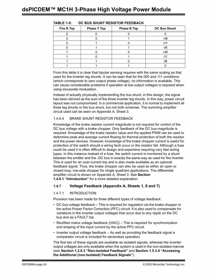
TABLE 1-5: DC BUS SHUNT RESISTOR FEEDBACK
From this table it is clear that bipolar sensing requires with the same scaling as that
used for the inverter leg shunts. It can be seen that for the 000 and 111 conditions
(which corresponds to zero output phase voltage), no information is available. This
can cause considerable problems if operation at low output voltages is required when
using sinusoidal modulation.
Instead of actually physically implementing the bus shunt, in this design, the signal
has been derived as the sum of the three inverter leg shunts. In this way, power circuit
layout was not compromised. In a commercial application, it is normal to implement all
three leg shunts or the bus shunt, but not both schemes. The summing amplifier
circuit used can be seen on Appendix A, Sheet 3.
1.4.6.4 BRAKE SHUNT RESISTOR FEEDBACK
Knowledge of the brake resistor current magnitude is not required for control of the
DC bus voltage with a brake chopper. Only feedback of the DC bus magnitude is
required. Knowledge of the brake resistor value and the applied PWM can be used to
determine peak and average current flowing for thermal protection of both the resistor
and the power devices. However, knowledge of the brake chopper current is useful for
protection of the switch should a wiring fault occur or the resistor fail. Although a fuse
could be used it is often difficult to design and expensive requiring very fast acting
types. In this instance instead of a fuse, the switch current is monitored by a shunt
between the emitter and the -DC bus in exactly the same way as used for the inverter.
This is used for an over-current trip and is also made available as an optional
feedback signal. Thus, the brake chopper can also be used as either an open or
closed loop, low-side chopper for single quadrant applications. The differential
amplifier circuit is shown on Appendix A, Sheet 3. See Section
1.4.6.1 “Introduction” for a more detailed explanation.
1.4.7 Voltage Feedback (Appendix A, Sheets 1, 6 and 7)
1.4.7.1 INTRODUCTION
Provision has been made for three different types of voltage feedback:
• DC bus voltage feedback – This is required for regulation via the brake chopper or
the active Power Factor Correction (PFC) circuit. It is also used to compensate for
variations in the inverter output voltages that occur due to any ripple on the DC
bus and as a FAULT trip.
• Rectified mains voltage feedback (|VAC|) – This is required for synchronization
and shaping of the input current by the active PFC circuit.
• Inverter output voltage feedback – As well as providing the feedback signal a
comparator circuit is included for sensorless operation.
The first two of these signals are available as isolated signals, whereas the inverter
output voltages are only available when the system is used in the non-isolated manner
(see Section 1.2.6.3 “Non-isolated Feedback” and Section 1.5.3.4 “Accessing
the Additional (non-isolated) Feedback Signals”).
Fire R Top Phase Y Top Phase B Top DC Bus Shunt
0 0 0 0
0 0 1 +IB
0 1 0 +IY
0 1 1 -IR
1 0 0 +IR
1 0 1 -IY
1 1 0 -IB
1 1 1 0
DS70096A-page 24 © 2003 Microchip Technology Inc.
Set Up and Operation
1.4.7.2 ISOLATED VOLTAGE FEEDBACK
There are many different ways that the two isolated voltage feedback signals can be
provided. Clearly, the DC level must be correctly maintained while still giving sufficient
bandwidth. The bandwidth is especially important for the |VAC| signal in order to
ensure low harmonics are produced by the active PFC. Power supply consumption
should also be as low as possible. All the above requirements can be met by the use
of an inexpensive PIC® microcontroller, along with two additional low current
optocouplers.
In this case, an 8-pin PIC12C671 microcontroller was chosen, as it has the necessary
ADC on-board and is low cost. Full advantage could be taken of the on-board 4 MHz
RC clock. Three different methods for representing the magnitude of the two signals
were considered. In all cases, only two optocouplers were required.
• A serial communication interface – A simplified two-wire SPI (Clock and Data
Out). It would operate as a master with the dsPIC device as the slave. Given the
PIC12C671 does not have a hardware SPI module, the interface would be
reproduced in software. The code latency was to be used for ADC acquisition and
conversion timing. This was the method chosen and the code is given in
Appendix B along with a diagram showing the transmission data cycle.
• Pulse width modulation at constant frequency – This was rejected partly due to
concerns over distortion of the pulse width by economic optocouplers. Also, it was
thought that it would not be possible to provide the required bandwidth, while
maintaining the 8-bit resolution of the captured data, given the lack of a hardware
PWM module.
• Frequency modulation – This was considered given that the pulse distortion by
the optocouplers ceased to be an issue. However, concerns about how the band-
width of the feedback could be maintained over the 8-bit data range led to its
rejection.
The actual hardware is described below:
• U34 – The PIC12C671. Note that the PIC12C671 is reset whenever the RESET
line is asserted, as this pin has been configured as the MCLR. This allows correct
synchronization of the SPI with the dsPIC device to be established. The RESET
line must be asserted for a minimum pulse width of 2 µs.
• R12, R15, R122 – These form a potential divider so that the maximum expected
voltage on |VAC|_SENSE is 4.5V.
• C43 – This acts to smooth out any noise spikes on the |VAC|_SENSE_POINT in
combination with R12, R15 and R122.
• R10, R13, R14, R140, R141 – These form a potential divider so that the maximum
expected voltage on BUS_SENSE is 4.5V. Note that HALF_BUS_SENSE is used
by the sensorless position detection comparators (see Section 1.4.7.3 “Inverter
Output Voltage Feedback and Sensorless Detection”).
• C57 – This acts to filter out any noise spikes on the DC bus voltage sensing
circuit.
• D40, D42 – Clamping diodes to protect the PIC12C671 inputs.
Note: The clock and data signals for the SPI interface are inverted due to the
opto-isolators. The user code should account for this by sampling the data
on the falling clock edge and inverting the received data.
© 2003 Microchip Technology Inc. DS70096A-page 25
dsPICDEM™ MC1H 3-Phase High Voltage Power Module
• U16, U17 – Low current (1.6 mA), medium speed (1 MHz) optocouplers to provide
the isolation for the clock and data lines.
• R149, R150 – Series resistors that help to set the current through the optocoupler
emitters. They are sized to allow a minimum of 1.8 mA to flow.
• C64, C70 – Speed up capacitors to help reduce the effect of the optocoupler's
emitter capacitance at high data rates.
• R170, R171 – Pull-up resistors for the open collector outputs of U16 and U17.
1.4.7.3 INVERTER OUTPUT VOLTAGE FEEDBACK AND SENSORLESS
DETECTION
Knowledge of the actual inverter output voltage is useful for two different uses. The
first is for accurately compensating for output voltage errors due to dead time and
power device voltage drops. This can be especially important for high current low
voltage systems with high PWM frequencies and high performance requirements. The
second use is for back EMF sensing for sensorless position detection schemes for
Brushless Permanent Magnet (BPM) and other types of motors.
The hardware for providing this is now discussed with reference to the RED phase.
The other two phases have identical circuits.
• R20, R21 and R144 – A resistor divider chain with scaling, the same as the DC
voltage feedback. The same scaling is required in order that the “back EMF
crossing” detection works correctly. The scaling is such that the maximum
expected output voltage will give 4.5V.
• C61 – This provides filtering of the inverter output voltage in combination with
R20, R21 and R144.
• D41 – This provides a clamp to ensure R_VPH_SENSE is protected.
• U31-B – A comparator used to provide a simple sensorless position detection
scheme for BPM motors. Whenever R_PH crosses half the DC bus voltage, an
output transition will occur. The R_CROSSING signal is only valid during regions
of the electrical cycle, where the RED phase output current is zero, so that the
back EMF of the motor determines the voltage of R_VPH. Thus the scheme is
only suitable for use on BPM motors where 120 degree conduction scheme is
used. Careful decoding of all three crossing signals and appropriate angle
interpolation is required for correct commutation. An alternative method for
commutation feedback must be used near zero speed where the back EMF is
insufficient for the scheme to work.
• R143, R147 – These provide a small amount of hysteresis to prevent oscillation of
R_CROSSING.
• R142 – The pull-up resistor for the open-collector output of the comparator.
DS70096A-page 26 © 2003 Microchip Technology Inc.
Set Up and Operation
1.4.8 Firing Signal Isolation and Low Voltage Power Supplies
1.4.8.1 INTRODUCTION
The choice of isolation strategy and how the low voltage power supplies are to be
derived are two of the major decisions that determine the architecture of a motor drive
controller. For this design, the requirement was for flexibility while maintaining user
safety. It was essential that the system could work off a wide range of input voltages.
1.4.8.2 FIRING SIGNAL ISOLATION (APPENDIX A, SHEET 5)
Either optical or transformer-based isolation strategies can be used for transmitting
gate firing commands. For this design, it was decided to use optocouplers, as it was
possible that a particular firing command may be used for commutation as opposed to
high frequency modulation. This could lead to transformer saturation at low speeds.
The hardware implemented is described below:
• U6-U13 – HCPL4503 optocouplers. These parts were chosen to provide good
noise immunity, while requiring low current consumption on the output side.
Speed was also a consideration, so that too much delay or pulse distortion was
not introduced.
• R153-R160 – Pull-up resistors for the open collector outputs of the optocouplers.
• R162-169 – Series resistors to ensure at least 18 mA flows through the emitter
stage of the optocouplers. Note that the ground return is via a transistor (Q15) that
allows shutdown during detection of an over-current from one of the isolated Hall
effect current transducers.
• U32 and U33 – Schmitt-triggered inverters which clean up the edges from the
outputs of the optocouplers.
1.4.8.3 LOW VOLTAGE POWER SUPPLIES (APPENDIX A, SHEET 5 AND 8)
The requirement for operation over a wide range of input voltage resulted in using the
+5V supply coming from the control board as the power source for all the low voltage
power supplies. This was true for both the isolated and live sides of the system. The
power supply circuitry on the live side is described below:
• U18 – An isolating (3 kV rated) 1W unregulated DC-DC converter with 5V input
and 15V (nominal) output. The +15V supply is used for the gate drive of the power
devices and the comparators on the live side of the isolation barrier.
• L4 and C83: A filter to reduce the reflected ripple on the +5V supply from the
control board caused by the DC-DC converter.
• L3 and C77: A filter to reduce the magnitude of the ripple on the live +15V supply.
• U5 – A 5V linear regulator for the live control circuit supplies.
• D4 – A 1A diode to protect U5 against reverse bias during power-down.
• R61 – A 0Ω resistor linking the low voltage power supply star point to the -DC bus.
© 2003 Microchip Technology Inc. DS70096A-page 27
dsPICDEM™ MC1H 3-Phase High Voltage Power Module
1.4.9 FAULT Protection (Appendix A, Sheets 4, 5 and 6)
1.4.9.1 INTRODUCTION
Given the development nature of the system, robust independent FAULT protection is
provided on the power board rather than relying on software intervention. Five
different fault categories are used to indicate a FAULT to the user. Four of the fault
categories are detected on the live side. All FAULTs are latched and automatically
disable all firing commands. In a commercial application using the dsPIC device,
much of the hardware described below may be eliminated. In particular, the latches
are not required as the Output Compare and Motor Control PWM modules both have
dedicated fault inputs that can be configured to shutdown PWM outputs to their
inactive state.
The operation of the fault action is described below:
• D35-D38 and R114: These form an active high wire OR of all four (live) FAULT
signals. R114 provides a passive pull-down during normal operation. The resulting
FAULT signal is used to directly shutdown the inverter gate drive ICs via their
shutdown logic input.
• R113, Q13, R110, D34 and Q14: These components act to shutdown the PFC and
brake chopper during a FAULT. Q14 must be on for the detector stage of their
optocouplers to be powered. Under normal conditions, D34 and R110 provide the
base current for Q14. If the FAULT line is asserted, causing Q13 to turn on, or if
the +15V supply drops below approximately 10V, then Q14 turns off.
• U15 and R151: If FAULT is asserted, current flows via R151 to cause the
(open-collector) output of U15 to turn on. This indicates back to the isolated side
that a FAULT has occurred on the live side.
• R176 and Q15: If a Hall over-current is detected on the isolated side, the base
current for Q15 that normally flows via R176 is removed. As all the firing command
optocoupler emitters return via Q15, when Q15 is off, no firing can take place.
• D43, D44 and R172: These form an active low wire OR of the isolated and live
fault indications for feedback to the dsPIC device.
1.4.9.2 INVERTER SHUNT OVER-CURRENT
The feedback signals from the inverter leg shunts and the bus current signal derived
from them (see Section 1.4.6.2 “Inverter Leg Shunt Resistor Feedback” and
Section 1.4.6.3 “DC Bus Shunt Resistor Feedback”) are used to detect over
current trips. Note that the shunts will see “shoot-through” events which bypass the
Hall current sensors. The circuitry used to implement this is described below:
• U25 – A quad package comparator used for the over current threshold
comparisons. Each comparator has a small amount of hysteresis (formed by R119
and R120 for example) to ensure no output chattering occurs. Note that the
inverter leg shunts are compared for positive current, which is when the current is
flowing in a switch. The bus shunt is compared for a negative value to protect
against faults during braking/generating. R109 forms the pull-up for the open
collector outputs of U25. A small amount of filtering is used (e.g., R118, C45) to
prevent spikes on the shunt signals causing false trips.
• U27-B – A remaining Op Amp package used to generate the HIGH_REF (+4.5V)
from the Microchip MCP1525 2v5 reference.
• U26 (A and B) – Two, two-input NAND gates configured as a SET dominant SR
flip-flop. The SET dominance is important to ensure correct fault action even if the
RESET input is active.
• D5, R202 – An LED and its associated current limiting resistor for the visual
indication of the FAULT.
DS70096A-page 28 © 2003 Microchip Technology Inc.
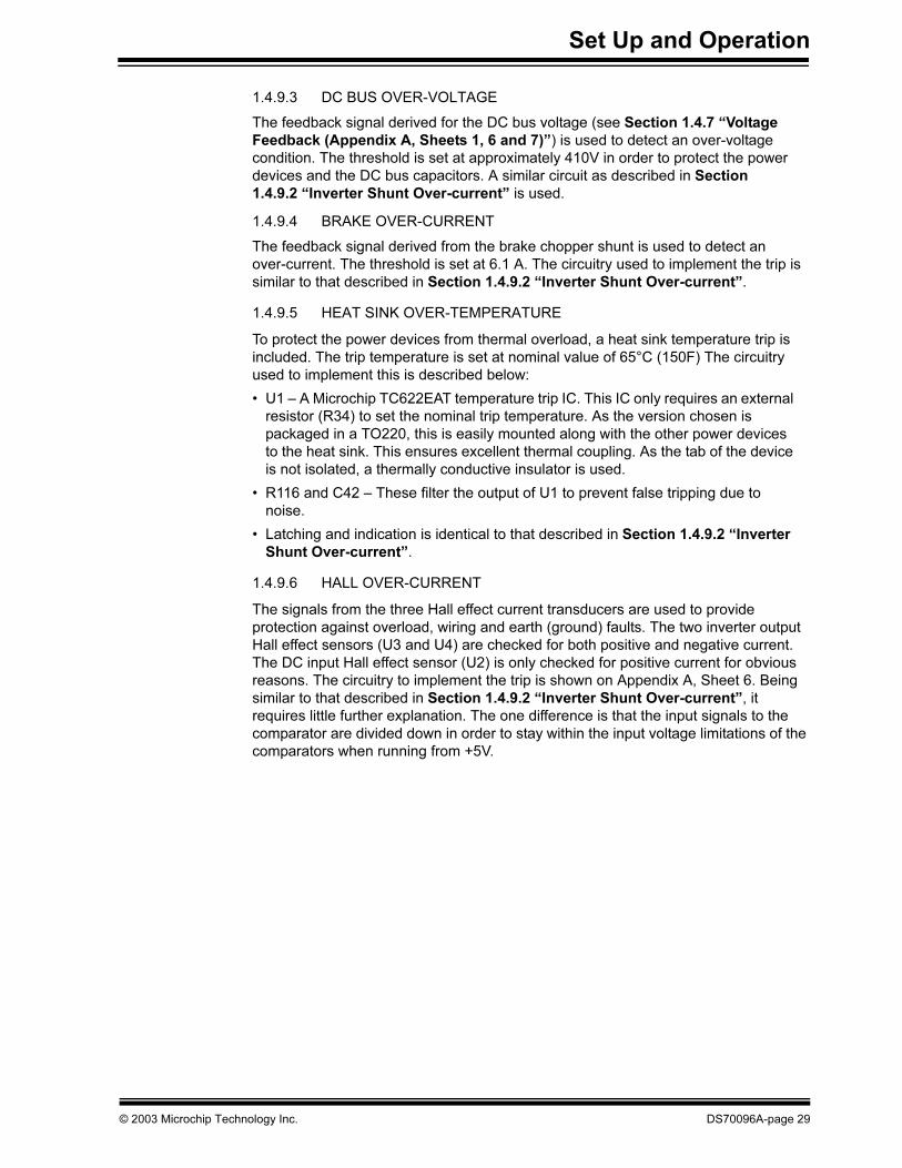
Set Up and Operation
1.4.9.3 DC BUS OVER-VOLTAGE
The feedback signal derived for the DC bus voltage (see Section 1.4.7 “Voltage
Feedback (Appendix A, Sheets 1, 6 and 7)”) is used to detect an over-voltage
condition. The threshold is set at approximately 410V in order to protect the power
devices and the DC bus capacitors. A similar circuit as described in Section
1.4.9.2 “Inverter Shunt Over-current” is used.
1.4.9.4 BRAKE OVER-CURRENT
The feedback signal derived from the brake chopper shunt is used to detect an
over-current. The threshold is set at 6.1 A. The circuitry used to implement the trip is
similar to that described in Section 1.4.9.2 “Inverter Shunt Over-current”.
1.4.9.5 HEAT SINK OVER-TEMPERATURE
To protect the power devices from thermal overload, a heat sink temperature trip is
included. The trip temperature is set at nominal value of 65°C (150F) The circuitry
used to implement this is described below:
• U1 – A Microchip TC622EAT temperature trip IC. This IC only requires an external
resistor (R34) to set the nominal trip temperature. As the version chosen is
packaged in a TO220, this is easily mounted along with the other power devices
to the heat sink. This ensures excellent thermal coupling. As the tab of the device
is not isolated, a thermally conductive insulator is used.
• R116 and C42 – These filter the output of U1 to prevent false tripping due to
noise.
• Latching and indication is identical to that described in Section 1.4.9.2 “Inverter
Shunt Over-current”.
1.4.9.6 HALL OVER-CURRENT
The signals from the three Hall effect current transducers are used to provide
protection against overload, wiring and earth (ground) faults. The two inverter output
Hall effect sensors (U3 and U4) are checked for both positive and negative current.
The DC input Hall effect sensor (U2) is only checked for positive current for obvious
reasons. The circuitry to implement the trip is shown on Appendix A, Sheet 6. Being
similar to that described in Section 1.4.9.2 “Inverter Shunt Over-current”, it
requires little further explanation. The one difference is that the input signals to the
comparator are divided down in order to stay within the input voltage limitations of the
comparators when running from +5V.
© 2003 Microchip Technology Inc. DS70096A-page 29

dsPICDEM™ MC1H 3-Phase High Voltage Power Module
1.5 MODIFYING THE BOARD
1.5.1 Introduction
Certain modifications have been allowed for in the design of the system, as described
below. Clearly, any additional modifications that the user chooses to make can not be
guaranteed to be functional or safe. It is assumed that relevant qualified personnel
only will use the system.
1.5.2 Accessing The System
Before removing the lid of the system, the following procedure should be rigidly
followed:
• Turn off all power to the system.
• Wait a minimum of 3 minutes so that the internal discharge circuit has reduced the
DC bus voltage to a safe level. The red LED bus voltage indicator visible through
the top ventilation holes should be out.
• Verify with a voltmeter that discharge has taken place by checking the potential
between the + and - DC terminals of the 7-pin output connector before
proceeding. The voltage should be less than 10V.
• The system is now safe to work on.
• Remove all cables from the system.
• Remove the screws fixing the lid to the chassis and heat sink on the top and
bottom.
• Slide the lid forwards while holding the unit by the heat sink.
1.5.3 Changing Current Feedback and Trip Scaling
Provision has been made to change the current feedback scaling of both the isolated
Hall effect transducers and the inverter leg and bus shunts. As the trip levels are set at
a fixed voltage, changing the feedback scaling also changes the trip levels. Changing
the scaling is accomplished in the following way:
• Follow the procedure given in Section 1.5.2 “Accessing The System” for
accessing the unit.
• Changing the inverter leg shunt sensing between unipolar and bipolar is
accomplished with LK4. LK4 is located directly under the “Danger High Voltage”
label on the PCB as shown in Section 9. Table 1-6 shows the settings:
TABLE 1-6: SHUNT FEEDBACK POLARITY SELECTION
LK 4 Setting Feedback Range
1-2 Bipolar
2-3 Unipolar
DS70096A-page 30 © 2003 Microchip Technology Inc.
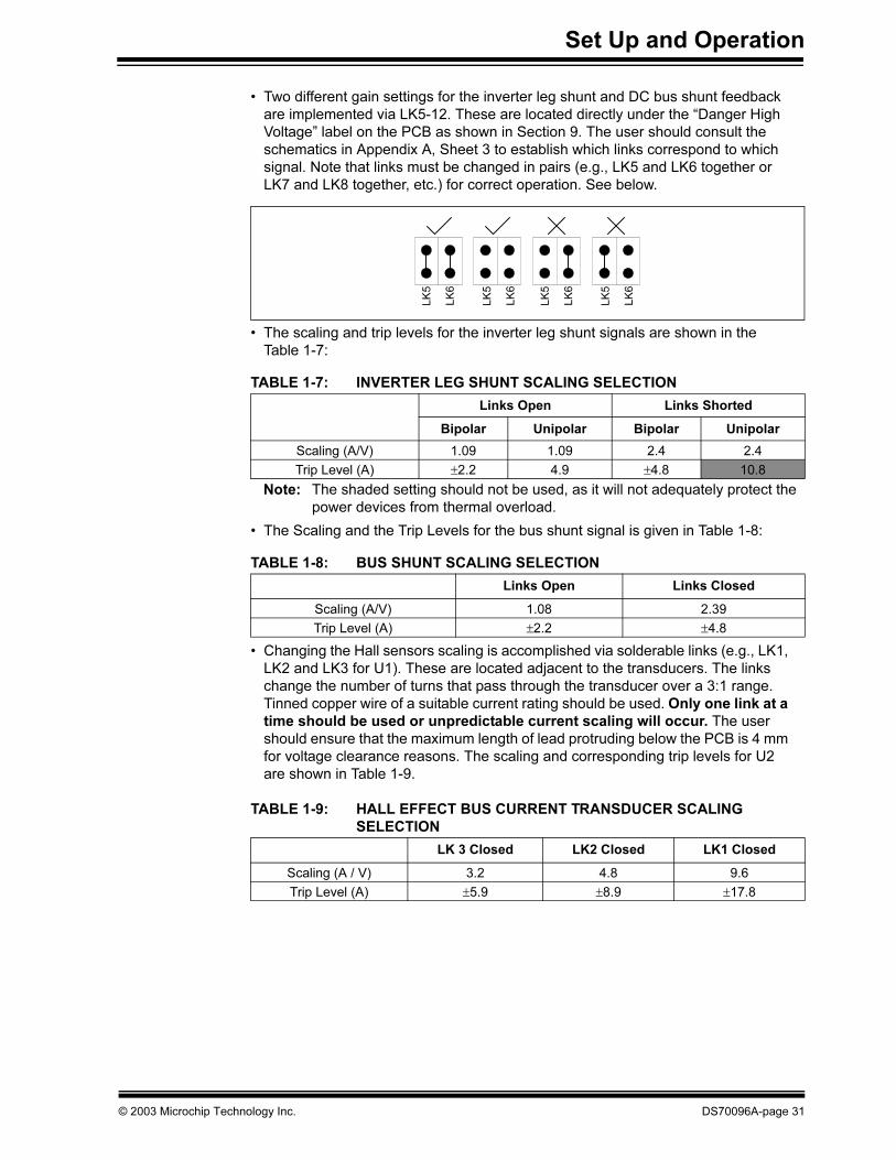
Set Up and Operation
• Two different gain settings for the inverter leg shunt and DC bus shunt feedback
are implemented via LK5-12. These are located directly under the “Danger High
Voltage” label on the PCB as shown in Section 9. The user should consult the
schematics in Appendix A, Sheet 3 to establish which links correspond to which
signal. Note that links must be changed in pairs (e.g., LK5 and LK6 together or
LK7 and LK8 together, etc.) for correct operation. See below.
• The scaling and trip levels for the inverter leg shunt signals are shown in the
Table 1-7:
TABLE 1-7: INVERTER LEG SHUNT SCALING SELECTION
• The Scaling and the Trip Levels for the bus shunt signal is given in Table 1-8:
TABLE 1-8: BUS SHUNT SCALING SELECTION
• Changing the Hall sensors scaling is accomplished via solderable links (e.g., LK1,
LK2 and LK3 for U1). These are located adjacent to the transducers. The links
change the number of turns that pass through the transducer over a 3:1 range.
Tinned copper wire of a suitable current rating should be used. Only one link at a
time should be used or unpredictable current scaling will occur. The user
should ensure that the maximum length of lead protruding below the PCB is 4 mm
for voltage clearance reasons. The scaling and corresponding trip levels for U2
are shown in Table 1-9.
TABLE 1-9: HALL EFFECT BUS CURRENT TRANSDUCER SCALING
SELECTION
Links Open Links Shorted
Bipolar Unipolar Bipolar Unipolar
Scaling (A/V) 1.09 1.09 2.4 2.4
Trip Level (A) ±2.2 4.9 ±4.8 10.8
Note: The shaded setting should not be used, as it will not adequately protect the
power devices from thermal overload.
Links Open Links Closed
Scaling (A/V) 1.08 2.39
Trip Level (A) ±2.2 ±4.8
LK 3 Closed LK2 Closed LK1 Closed
Scaling (A / V) 3.2 4.8 9.6
Trip Level (A) ±5.9 ±8.9 ±17.8
LK5
LK6
LK5
LK6
LK5
LK6
LK5
LK6
© 2003 Microchip Technology Inc. DS70096A-page 31
dsPICDEM™ MC1H 3-Phase High Voltage Power Module
• If the user has bypassed the PFC diode or even the entire PFC section (see
Section 1.5.3.3 “Bypassing The PFC”) then LK1 for U2 may be used to allow
higher peak input currents while still ensuring ground FAULT protection is active.
Alternatively if the user wishes to develop a low power PFC application, then LK3
may be used for improved feedback sensitivity.
• The scaling of U3 and 4 is different from that shown above. This is because the
output leads are also passed through the transducers thereby giving an additional
turn for increased sensitivity. The scaling and trip levels for U3 and U4 are shown
in Table 1-10.
TABLE 1-10: INVERTER LEG CURRENT TRANSDUCER SCALING SELECTION
• Once the modification is complete, install the lid ensuring all the screws are
replaced.
1.5.3.1 CHANGING VOLTAGE FEEDBACK AND TRIP SCALING
The voltage feedback scaling is configured for the maximum range of input voltages. If
the user requires full ADC resolution at lower voltages, then this can easily be
accomplished by changing the high voltage resistors mounted on the top of the PCB.
• Follow the procedure given in Section 1.5.2 “Accessing The System” for
accessing the unit.
• To change DC bus voltage scaling, modify R10, R13, R14. Note, if using the back
EMF crossing detection circuitry (see Section 1.4.7.3 “Inverter Output Voltage
Feedback and Sensorless Detection”), the user should also change the phase
voltage feedback resistors to ensure consistent scaling.
• To change |VAC| voltage scaling modify R12 and R15.
• To change phase voltage scaling modify R16-R20.
• In all cases, it is suggested that the changes be made from the top of the board. If
new component legs are inserted, these should be cropped to ensure that the
maximum length of lead protruding below the PCB is 4 mm.
• Once the modification is complete, install the lid ensuring all the screws are
replaced.
LK 15/18 Closed LK14/17 Closed LK13/16 Closed
Scaling (A / V) 2.4 3.2 4.8
Trip Level (A) ±4.4 ±5.9 ±8.9
Caution: Owing to thermal limitations of the inverter power devices, the user
should be very careful about changing the scaling of U3 and 4. If the
user has robust current regulation and stall detection software then
LK14 and LK17 may be used to allow higher output currents. However
the power devices will only be sufficiently cooled if PWM duty cycles do
not exceed 75% below 10 Hz fundamental output frequency. Under no
circumstances should LK13 and LK16 be used, as adequate thermal
protection of the power devices is not provided.
DS70096A-page 32 © 2003 Microchip Technology Inc.
Set Up and Operation
1.5.3.2 MODIFYING OR REMOVING THE INTERNAL BRAKING RESISTOR
The type of braking resistor installed on the heat sink allows a maximum continuous
dissipation of 50W, but can tolerate many times this power level for short periods. The
value installed as standard only allows a maximum dissipation of 35W owing to its
high resistance. If the user wishes to change the resistor to a lower value or remove
the resistor completely as they are using an external resistor, then they should follow
the procedure given below.
• Follow the procedure given in Section 1.5.2 “Accessing The System” for
accessing the unit.
• De-solder or cut the wires to J7 and J8. This can be done from the top of the PCB.
• Undo the screws attaching the resistor to the heat sink and remove the resistor
and its wiring.
• If not fitting a new resistor, proceed to the last step.
• Make up a wiring assembly for the new resistor with similar lead lengths and the
terminals protected with heat shrink sleeving. Ensure the wire has sufficient
current and voltage rating (600V).
• Apply a thin, even coating of thermally conductive heat sink compound (e.g.,
Dow-Corning 340) to the back of the resistor.
• Fit the resistor to the heat sink and solder the wires into J7 and J8. Ensure the
leads are cropped so that the maximum length of lead protruding below the PCB
is 4 mm.
• Once the modification is complete, install the lid ensuring all the screws are
replaced.
Note that if the user fits a lower value of internal resistor to allow higher transient
dissipation, then the user's software must ensure adequate thermal protection for the
resistor. Failure to do so can cause the resistor to rupture. Consult the manufacturers
data sheet carefully.
1.5.3.3 BYPASSING THE PFC
If the user does not require the use of the active Power Factor Correction, all the user
needs to do is not fire the PFC switch. The system will still benefit from the PFC
inductor acting to smooth the input current when the rectifier is charging the DC bus
capacitors. However, the PFC diode will remain in circuit. This will incur additional
unnecessary loss. Provision has therefore been made to bypass the PFC in two
different ways. Alternatively, the user could feed in an external DC supply using the
auxiliary DC input (see Section 1.2.2 “Making Power Connections”). The
procedures for bypassing the PFC is described below:
Keeping the PFC inductor in circuit:
• Follow the procedure given in Section 1.5.2 “Accessing The System” for
accessing the unit.
• De-solder the wire of the large toroidal inductor marked as L2 (2) near the
left-hand DC bus capacitor C4. This can be done from the top of the PCB.
• Solder the L2 wire into pad J4 ensuring that the maximum length of lead
protruding below the PCB is 4 mm.
• If required, replace the input fuse with a 6-7A part of the same type (Time Lag,
High Breaking Capacity and 250V or greater voltage rating).
• Once the modification is complete, install the lid ensuring all the screws are
replaced.
• Note that the maximum continuous limit on input current increases to 6A (RMS)
limited by the loss in the PFC inductor.
© 2003 Microchip Technology Inc. DS70096A-page 33

dsPICDEM™ MC1H 3-Phase High Voltage Power Module
Removing the PFC inductor from the circuit:
• Follow the procedure given in Section 1.5.2 “Accessing The System” for
accessing the unit.
• De-solder L1. This can be done from the top of the PCB.
• Solder a wire between J4 and J6. The wire size should be 1 mm2 (18 AWG) with a
minimum voltage rating of 600V and suitable for operation up to 105°C. Note that
the wire should be no longer than 75 mm (3") in length and should be cropped to
ensure that the maximum length of lead protruding below the PCB is 4 mm.
• If required, change the current scaling of U2 as given in Section 1.5.3 “Changing
Current Feedback and Trip Scaling”.
• If required, replace the input fuse with a 7-8A part of the same type (Time Lag,
High Breaking Capacity and 250V or greater voltage rating).
• Once the modification is complete, install the lid ensuring all the screws are
replaced.
• Note that the maximum continuous limit on input current increases to 7A (RMS)
limited by the soft start NTC.
1.5.3.4 ACCESSING THE ADDITIONAL (NON-ISOLATED) FEEDBACK SIGNALS
All the non-isolated feedback signals are brought to a series of links that run along the
edge of the isolation barrier. In order to access these signals, the user should rigidly
carry out the procedure given below. Failure to do so could represent a safety hazard
to the user as the isolation barrier is bridged.
• Follow the procedure given in Section 1.5.2 “Accessing The System” for
accessing the unit.
• Disconnect the input wiring from the AC supply outlet.
• Wire in a safety isolation transformer with a suitable rating between the AC supply
outlet and the AC input to the system. The supply to the unit should now be
“floating”.
• The user should satisfy themselves that the isolation transformer is wired correctly
and the insulation is intact.
• Ensure that the earth (ground) continuity is maintained to the unit.
• Solder a wire between J13 and J5. The wire should be 1.0-1.5 mm2 (18-16 AWG)
with a minimum voltage rating of 600V and suitable for operation up to 105°C. It
should be the standard color used for earth (ground) cabling in the user's country
(e.g., green for U.S.). This link is connecting the -DC bus to the incoming earth
(ground).
• In order to make the links for the non-isolated signals; it is recommended that two
0.3" pitch, 14-pin DIL resistor packages be used. These should be of the
“straight-through” type with 7 independent resistors. The suggested value is
330Ω, as this will provide some ESD protection without too high of a source
impedance being introduced. Note that LK28 has no circuit connections and is
provided to allow the second DIL resistor package to be installed. If the user
decides to fit links or individual resistors, these should be installed so that not
more than 4 mm of lead protrude beneath the PCB.
• Note that all signals to and from the system are now referenced to the -DC bus
that is at earth (ground) potential. The isolation transformer is providing the safety
isolation. The digital 0V of the control card is permanently connected to the
enclosure chassis and is therefore also referenced to ground.
• Once the modification is complete, install the lid ensuring all the screws are
replaced.
DS70096A-page 34 © 2003 Microchip Technology Inc.

Set Up and Operation
1.5.3.5 OTHER MODIFICATIONS
Clearly, there are many other modifications that an experienced engineer could make
to the system. These could include:
• Changing the inverter power devices for lower voltage devices (e.g., IRF644 250V
MOSFETs) if operation at low input voltages only is required.
• Changing the DC bus capacitors for higher capacitance lower voltage
components.
No guarantee or liability can be accepted for any modifications that the user makes to
the system. If the user removes the PCB from the enclosure chassis, they should
ensure that the power device clamping force and the insulation is unaltered when the
PCB is re-installed.
© 2003 Microchip Technology Inc. DS70096A-page 35
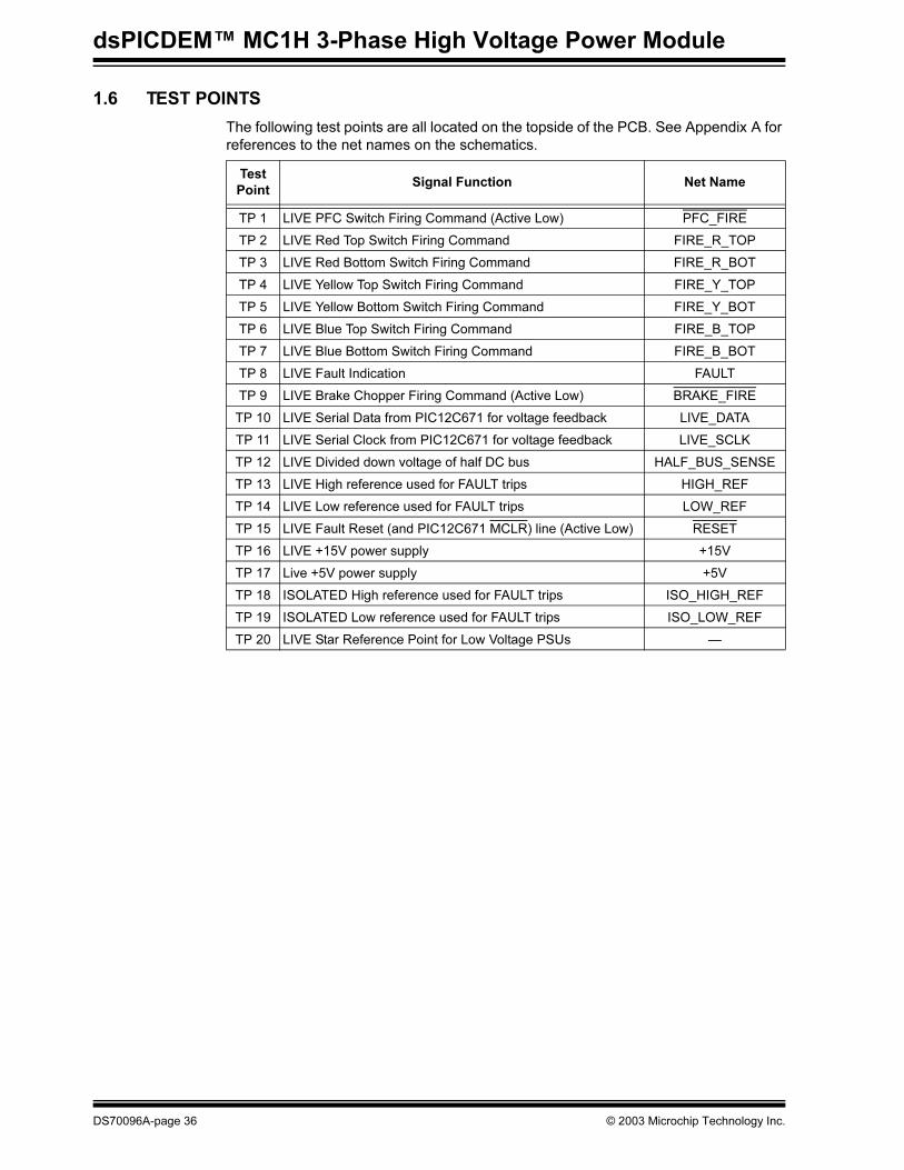
dsPICDEM™ MC1H 3-Phase High Voltage Power Module
1.6 TEST POINTS
The following test points are all located on the topside of the PCB. See Appendix A for
references to the net names on the schematics.
Test
PointSignal Function Net Name
TP 1 LIVE PFC Switch Firing Command (Active Low) PFC_FIRE
TP 2 LIVE Red Top Switch Firing Command FIRE_R_TOP
TP 3 LIVE Red Bottom Switch Firing Command FIRE_R_BOT
TP 4 LIVE Yellow Top Switch Firing Command FIRE_Y_TOP
TP 5 LIVE Yellow Bottom Switch Firing Command FIRE_Y_BOT
TP 6 LIVE Blue Top Switch Firing Command FIRE_B_TOP
TP 7 LIVE Blue Bottom Switch Firing Command FIRE_B_BOT
TP 8 LIVE Fault Indication FAULT
TP 9 LIVE Brake Chopper Firing Command (Active Low) BRAKE_FIRE
TP 10 LIVE Serial Data from PIC12C671 for voltage feedback LIVE_DATA
TP 11 LIVE Serial Clock from PIC12C671 for voltage feedback LIVE_SCLK
TP 12 LIVE Divided down voltage of half DC bus HALF_BUS_SENSE
TP 13 LIVE High reference used for FAULT trips HIGH_REF
TP 14 LIVE Low reference used for FAULT trips LOW_REF
TP 15 LIVE Fault Reset (and PIC12C671 MCLR) line (Active Low) RESET
TP 16 LIVE +15V power supply +15V
TP 17 Live +5V power supply +5V
TP 18 ISOLATED High reference used for FAULT trips ISO_HIGH_REF
TP 19 ISOLATED Low reference used for FAULT trips ISO_LOW_REF
TP 20 LIVE Star Reference Point for Low Voltage PSUs —
DS70096A-page 36 © 2003 Microchip Technology Inc.
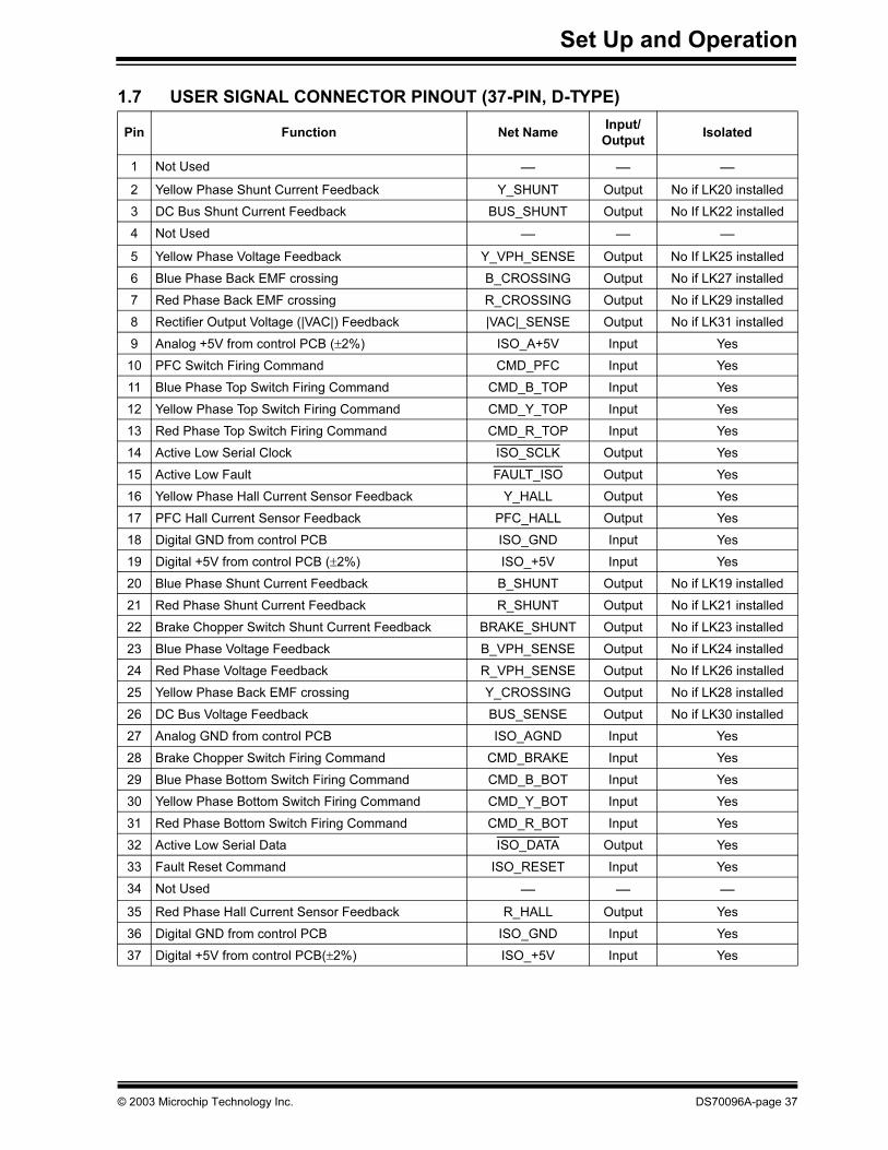
Set Up and Operation
1.7 USER SIGNAL CONNECTOR PINOUT (37-PIN, D-TYPE)
Pin Function Net NameInput/
OutputIsolated
1 Not Used — — —
2 Yellow Phase Shunt Current Feedback Y_SHUNT Output No if LK20 installed
3 DC Bus Shunt Current Feedback BUS_SHUNT Output No If LK22 installed
4 Not Used — — —
5 Yellow Phase Voltage Feedback Y_VPH_SENSE Output No If LK25 installed
6 Blue Phase Back EMF crossing B_CROSSING Output No if LK27 installed
7 Red Phase Back EMF crossing R_CROSSING Output No if LK29 installed
8 Rectifier Output Voltage (|VAC|) Feedback |VAC|_SENSE Output No if LK31 installed
9 Analog +5V from control PCB (±2%) ISO_A+5V Input Yes
10 PFC Switch Firing Command CMD_PFC Input Yes
11 Blue Phase Top Switch Firing Command CMD_B_TOP Input Yes
12 Yellow Phase Top Switch Firing Command CMD_Y_TOP Input Yes
13 Red Phase Top Switch Firing Command CMD_R_TOP Input Yes
14 Active Low Serial Clock ISO_SCLK Output Yes
15 Active Low Fault FAULT_ISO Output Yes
16 Yellow Phase Hall Current Sensor Feedback Y_HALL Output Yes
17 PFC Hall Current Sensor Feedback PFC_HALL Output Yes
18 Digital GND from control PCB ISO_GND Input Yes
19 Digital +5V from control PCB (±2%) ISO_+5V Input Yes
20 Blue Phase Shunt Current Feedback B_SHUNT Output No if LK19 installed
21 Red Phase Shunt Current Feedback R_SHUNT Output No if LK21 installed
22 Brake Chopper Switch Shunt Current Feedback BRAKE_SHUNT Output No if LK23 installed
23 Blue Phase Voltage Feedback B_VPH_SENSE Output No if LK24 installed
24 Red Phase Voltage Feedback R_VPH_SENSE Output No If LK26 installed
25 Yellow Phase Back EMF crossing Y_CROSSING Output No if LK28 installed
26 DC Bus Voltage Feedback BUS_SENSE Output No if LK30 installed
27 Analog GND from control PCB ISO_AGND Input Yes
28 Brake Chopper Switch Firing Command CMD_BRAKE Input Yes
29 Blue Phase Bottom Switch Firing Command CMD_B_BOT Input Yes
30 Yellow Phase Bottom Switch Firing Command CMD_Y_BOT Input Yes
31 Red Phase Bottom Switch Firing Command CMD_R_BOT Input Yes
32 Active Low Serial Data ISO_DATA Output Yes
33 Fault Reset Command ISO_RESET Input Yes
34 Not Used — — —
35 Red Phase Hall Current Sensor Feedback R_HALL Output Yes
36 Digital GND from control PCB ISO_GND Input Yes
37 Digital +5V from control PCB(±2%) ISO_+5V Input Yes
© 2003 Microchip Technology Inc. DS70096A-page 37

dsPICDEM™ MC1H 3-Phase High Voltage Power Module
NOTES:
DS70096A-page 38 © 2003 Microchip Technology Inc.
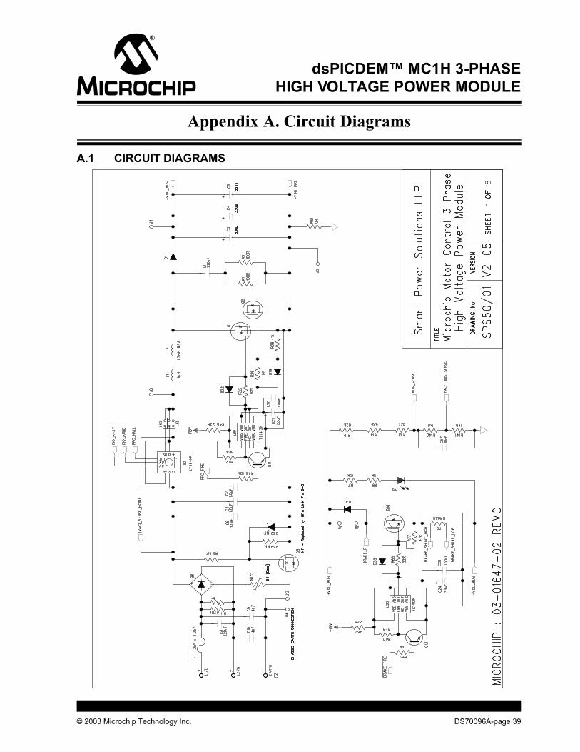
dsPICDEM™ MC1H 3-PHASE
HIGH VOLTAGE POWER MODULE
Appendix A. Circuit Diagrams
A.1 CIRCUIT DIAGRAMS
© 2003 Microchip Technology Inc. DS70096A-page 39
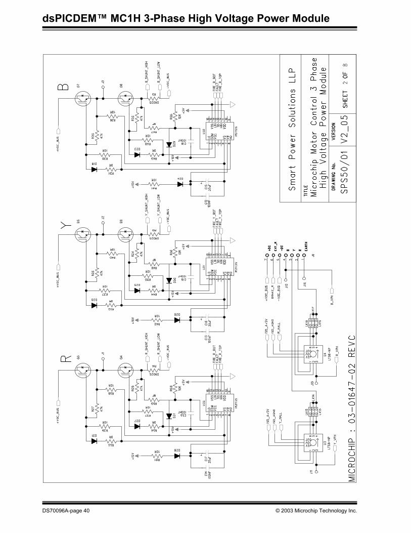
dsPICDEM™ MC1H 3-Phase High Voltage Power Module
DS70096A-page 40 © 2003 Microchip Technology Inc.
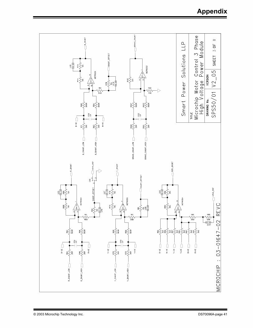
Appendix
© 2003 Microchip Technology Inc. DS70096A-page 41
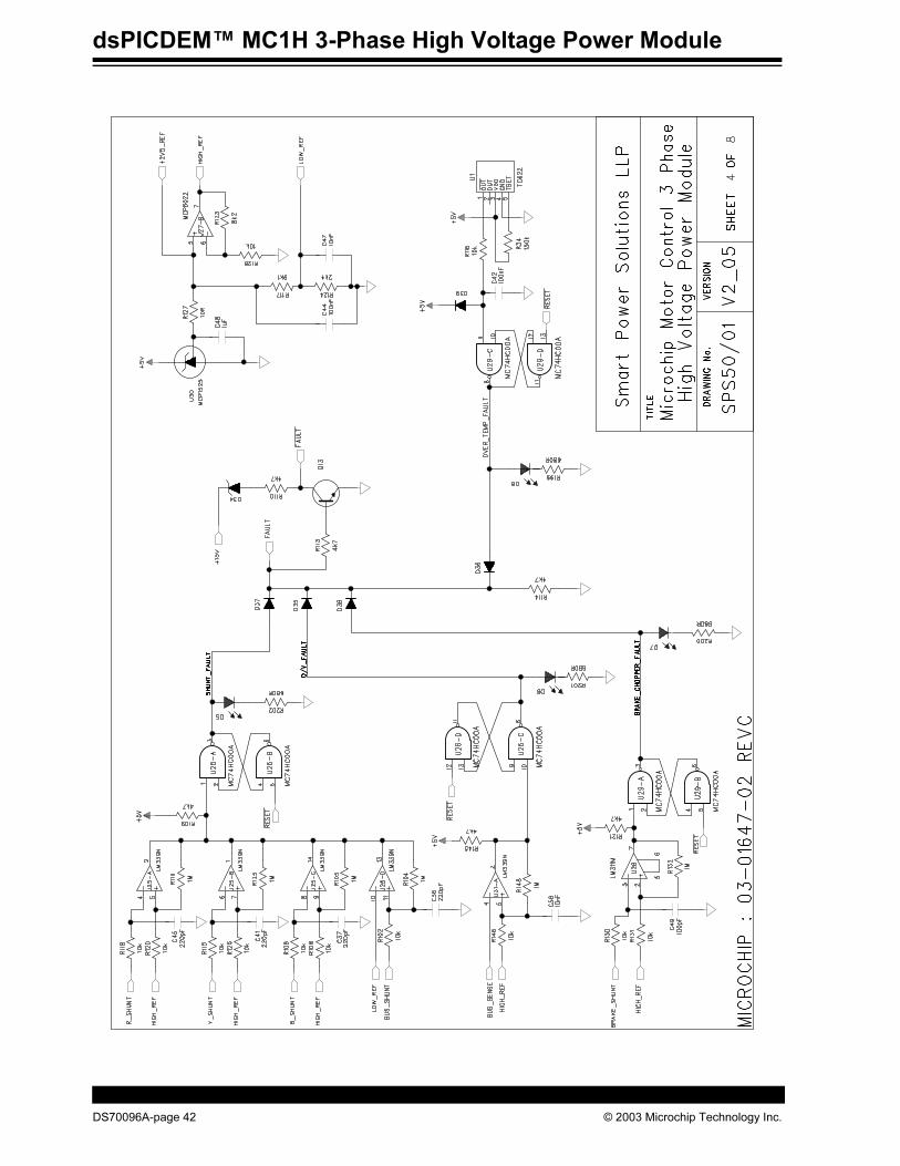
dsPICDEM™ MC1H 3-Phase High Voltage Power Module
DS70096A-page 42 © 2003 Microchip Technology Inc.
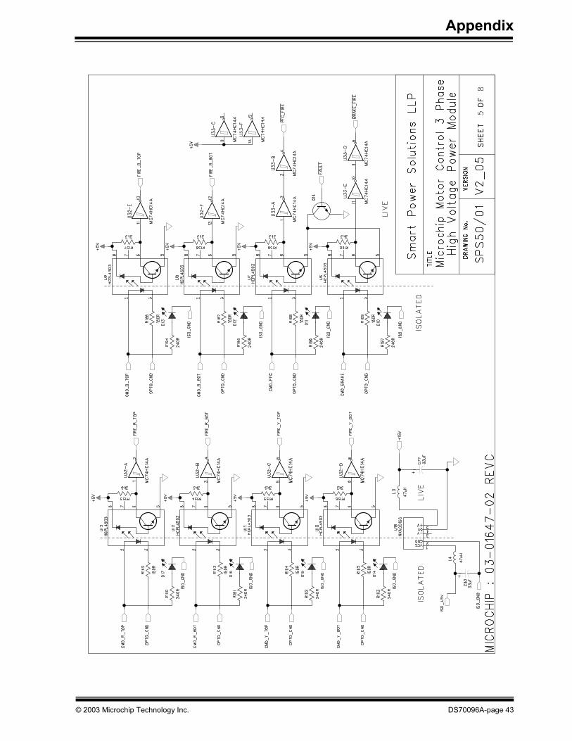
Appendix
© 2003 Microchip Technology Inc. DS70096A-page 43
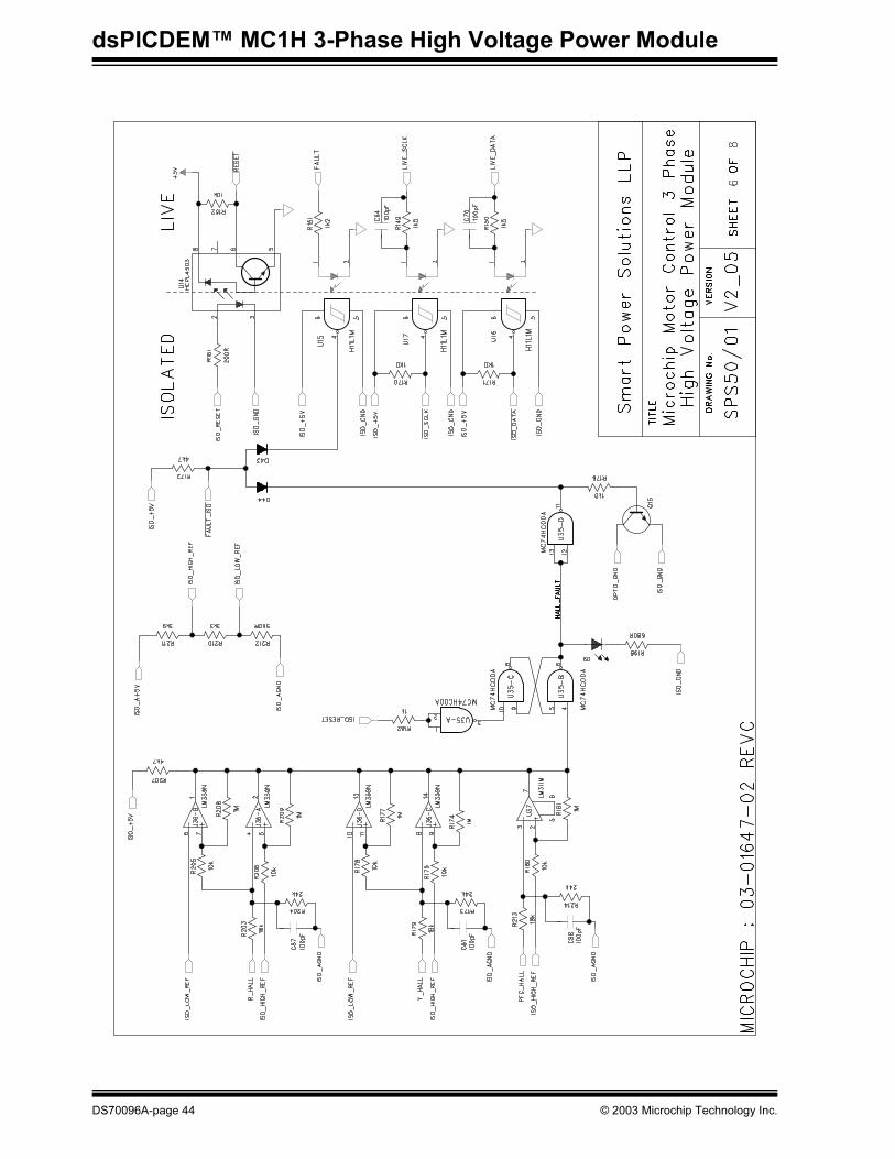
dsPICDEM™ MC1H 3-Phase High Voltage Power Module
DS70096A-page 44 © 2003 Microchip Technology Inc.
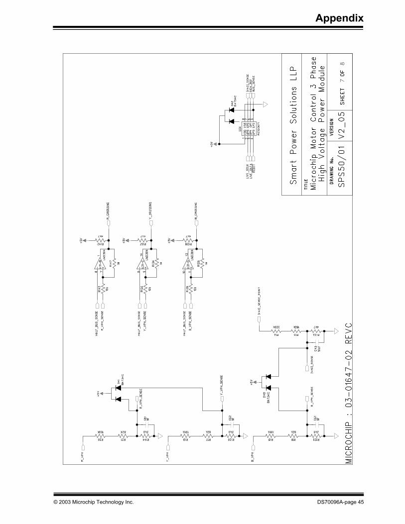
Appendix
© 2003 Microchip Technology Inc. DS70096A-page 45
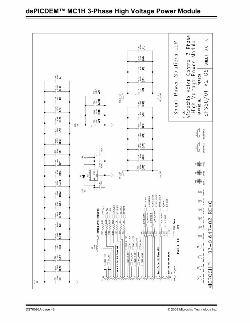
dsPICDEM™ MC1H 3-Phase High Voltage Power Module
DS70096A-page 46 © 2003 Microchip Technology Inc.
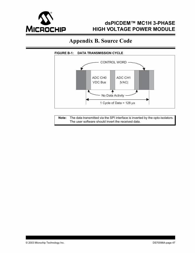
dsPICDEM™ MC1H 3-PHASE
HIGH VOLTAGE POWER MODULE
Appendix B. Source Code
FIGURE B-1: DATA TRANSMISSION CYCLE
ADC CH0
VDC Bus
ADC CH1
|VAC|
1 Cycle of Data = 128 µs
CONTROL WORD
No Data Activity
Note: The data transmitted via the SPI interface is inverted by the opto-isolators.
The user software should invert the received data.
© 2003 Microchip Technology Inc. DS70096A-page 47
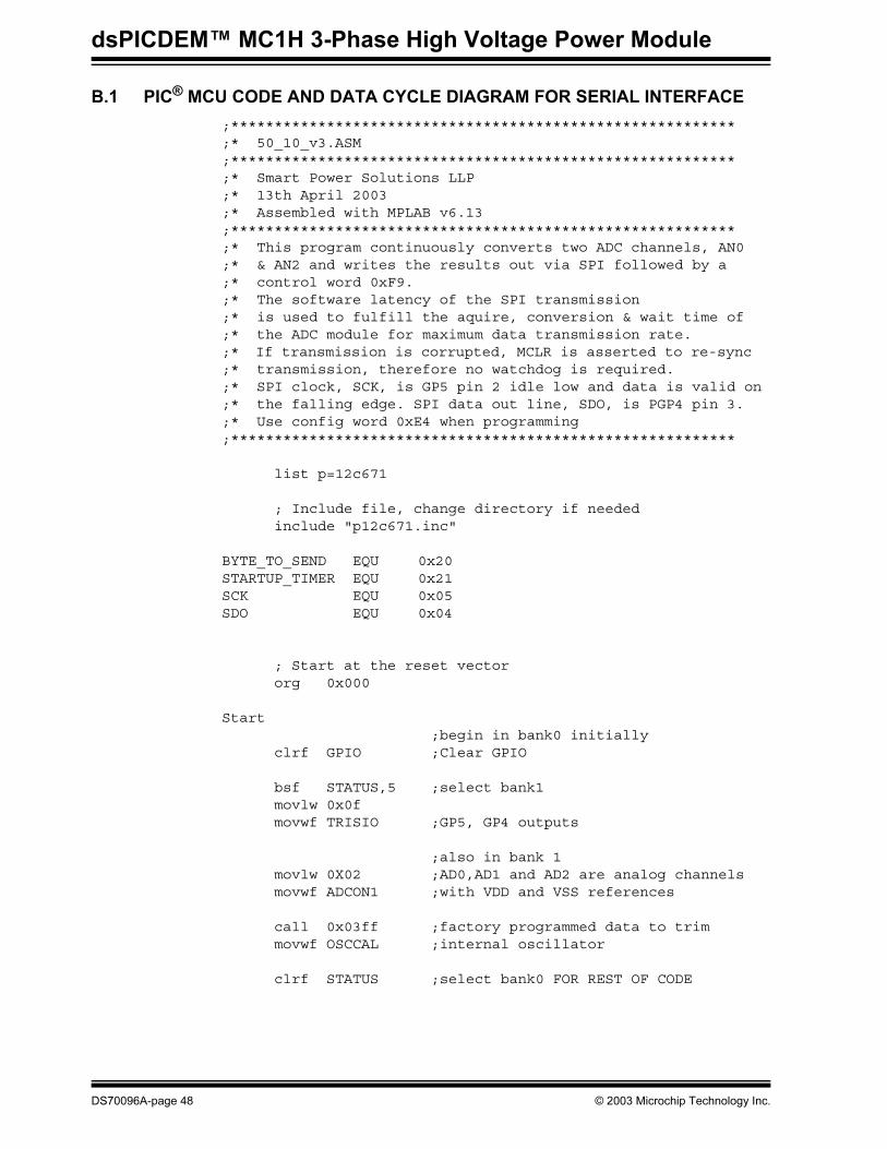
dsPICDEM™ MC1H 3-Phase High Voltage Power Module
B.1 PIC® MCU CODE AND DATA CYCLE DIAGRAM FOR SERIAL INTERFACE
;**********************************************************;* 50_10_v3.ASM;**********************************************************;* Smart Power Solutions LLP;* 13th April 2003;* Assembled with MPLAB v6.13;**********************************************************;* This program continuously converts two ADC channels, AN0 ;* & AN2 and writes the results out via SPI followed by a;* control word 0xF9.;* The software latency of the SPI transmission;* is used to fulfill the aquire, conversion & wait time of ;* the ADC module for maximum data transmission rate. ;* If transmission is corrupted, MCLR is asserted to re-sync ;* transmission, therefore no watchdog is required. ;* SPI clock, SCK, is GP5 pin 2 idle low and data is valid on ;* the falling edge. SPI data out line, SDO, is PGP4 pin 3.;* Use config word 0xE4 when programming;**********************************************************
list p=12c671
; Include file, change directory if neededinclude "p12c671.inc"
BYTE_TO_SEND EQU 0x20STARTUP_TIMER EQU 0x21SCK EQU 0x05SDO EQU 0x04
; Start at the reset vectororg 0x000
Start;begin in bank0 initially
clrf GPIO ;Clear GPIO
bsf STATUS,5 ;select bank1movlw 0x0fmovwf TRISIO ;GP5, GP4 outputs
;also in bank 1movlw 0X02 ;AD0,AD1 and AD2 are analog channelsmovwf ADCON1 ;with VDD and VSS references
call 0x03ff ;factory programmed data to trimmovwf OSCCAL ;internal oscillator
clrf STATUS ;select bank0 FOR REST OF CODE
DS70096A-page 48 © 2003 Microchip Technology Inc.

Appendix
Initial_Capture ;before starting SPI transmission, ;aquire &convert ADC ch0, BUS_SENSE
movlw 0x41 ;set:Fosc/8, A/D enable, ch0 selectmovwf ADCON0 ;begin sampling ch0
movlw 0x04 ;wait for approx 20us aquisition timemovwf STARTUP_TIMER
delaydecf STARTUP_TIMER,Fbtfss STATUS,Zgoto delay
bsf ADCON0,GO ;Start A/D conversion Channel 0
finish_1st_conversionbtfsc ADCON0,GO ;wait for end of conversion flaggoto finish_1st_conversion
movf ADRES,Wmovwf BYTE_TO_SEND
nop ;extra wait before starting new aquisi-tion
;**************************************************************
Mainmovlw 0x51 ;Fosc/8, A/D enabled, ch 2 selectedmovwf ADCON0 ;begin sampling channel 2 |VAC|_SENSE
;begin to transmit value from channel 0
bcf GPIO,SDO ;send bit 7bsf GPIO,SCKbtfsc BYTE_TO_SEND,7bsf GPIO,SDObcf GPIO,SCK
bcf GPIO,SDO ;send bit 6bsf GPIO,SCKbtfsc BYTE_TO_SEND,6bsf GPIO,SDObcf GPIO,SCK
bcf GPIO,SDO ;send bit 5bsf GPIO,SCKbtfsc BYTE_TO_SEND,5bsf GPIO,SDObcf GPIO,SCK
bcf GPIO,SDO ;send bit 4bsf GPIO,SCKbtfsc BYTE_TO_SEND,4bsf GPIO,SDObcf GPIO,SCK
© 2003 Microchip Technology Inc. DS70096A-page 49
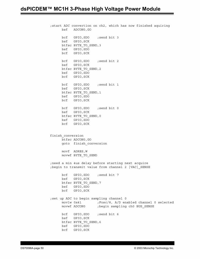
dsPICDEM™ MC1H 3-Phase High Voltage Power Module
;start ADC convertion on ch2, which has now finished aquiringbsf ADCON0,GO
bcf GPIO,SDO ;send bit 3bsf GPIO,SCKbtfsc BYTE_TO_SEND,3bsf GPIO,SDObcf GPIO,SCK
bcf GPIO,SDO ;send bit 2bsf GPIO,SCKbtfsc BYTE_TO_SEND,2bsf GPIO,SDObcf GPIO,SCK
bcf GPIO,SDO ;send bit 1bsf GPIO,SCKbtfsc BYTE_TO_SEND,1bsf GPIO,SDObcf GPIO,SCK
bcf GPIO,SDO ;send bit 0bsf GPIO,SCKbtfsc BYTE_TO_SEND,0bsf GPIO,SDObcf GPIO,SCK
finish_conversionbtfsc ADCON0,GOgoto finish_conversion
movf ADRES,Wmovwf BYTE_TO_SEND
;need a min 4us delay before starting next acquire;begin to transmit value from channel 2 |VAC|_SENSE
bcf GPIO,SDO ;send bit 7bsf GPIO,SCKbtfsc BYTE_TO_SEND,7bsf GPIO,SDObcf GPIO,SCK
;set up ADC to begin sampling channel 0movlw 0x41 ;Fosc/8, A/D enabled channel 0 selectedmovwf ADCON0 ;begin sampling ch0 BUS_SENSE
bcf GPIO,SDO ;send bit 6bsf GPIO,SCKbtfsc BYTE_TO_SEND,6bsf GPIO,SDObcf GPIO,SCK
DS70096A-page 50 © 2003 Microchip Technology Inc.

Appendix
bcf GPIO,SDO ;send bit 5bsf GPIO,SCKbtfsc BYTE_TO_SEND,5bsf GPIO,SDObcf GPIO,SCK
bcf GPIO,SDO ;send bit 4bsf GPIO,SCKbtfsc BYTE_TO_SEND,4bsf GPIO,SDObcf GPIO,SCK
bcf GPIO,SDO ;send bit 3bsf GPIO,SCKbtfsc BYTE_TO_SEND,3bsf GPIO,SDObcf GPIO,SCK
bcf GPIO,SDO ;send bit 2bsf GPIO,SCKbtfsc BYTE_TO_SEND,2bsf GPIO,SDObcf GPIO,SCK
bsf ADCON0,GO ;Start A/D conversion Channel 0
bcf GPIO,SDO ;send bit 1bsf GPIO,SCKbtfsc BYTE_TO_SEND,1bsf GPIO,SDObcf GPIO,SCK
bcf GPIO,SDO ;send bit 0bsf GPIO,SCKbtfsc BYTE_TO_SEND,0bsf GPIO,SDObcf GPIO,SCK
nopnopnopnop
;while ADC is still converting Channel 0, send control word 0xF9
bsf GPIO,SCK ;send bit7bsf GPIO,SDObcf GPIO,SCKnopbsf GPIO,SCK ;send bit6bcf GPIO,SCKnopbsf GPIO,SCK ;send bit5bcf GPIO,SCKnop
© 2003 Microchip Technology Inc. DS70096A-page 51
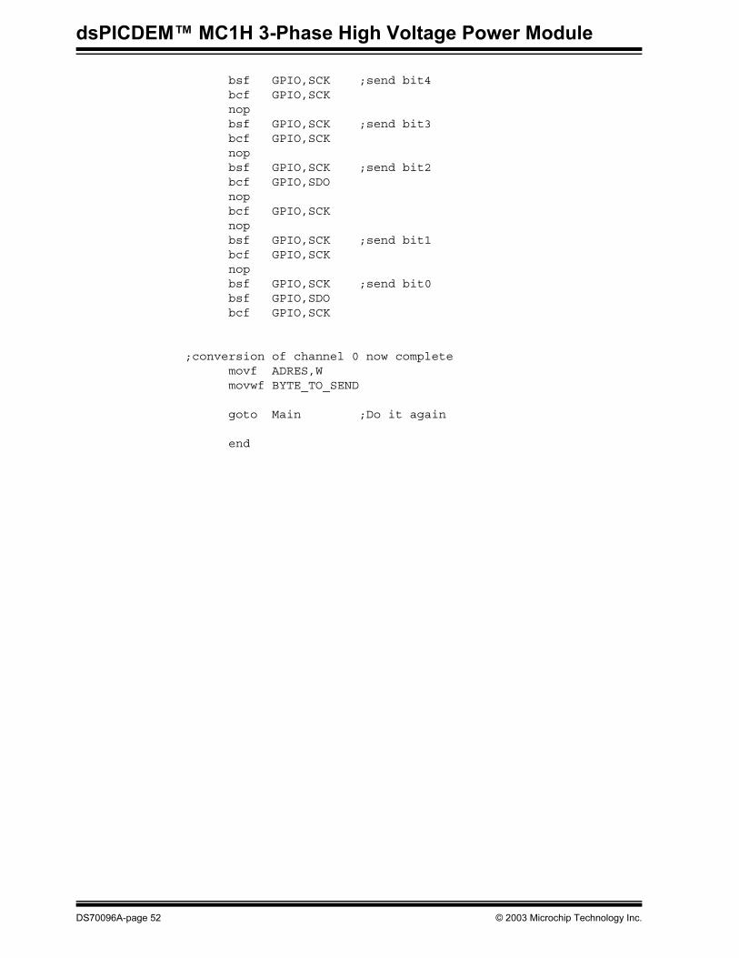
dsPICDEM™ MC1H 3-Phase High Voltage Power Module
bsf GPIO,SCK ;send bit4bcf GPIO,SCKnopbsf GPIO,SCK ;send bit3bcf GPIO,SCKnopbsf GPIO,SCK ;send bit2bcf GPIO,SDOnopbcf GPIO,SCKnopbsf GPIO,SCK ;send bit1bcf GPIO,SCKnopbsf GPIO,SCK ;send bit0bsf GPIO,SDObcf GPIO,SCK
;conversion of channel 0 now completemovf ADRES,Wmovwf BYTE_TO_SEND
goto Main ;Do it again
end
DS70096A-page 52 © 2003 Microchip Technology Inc.

Appendix
NOTES:
© 2003 Microchip Technology Inc. DS70096A-page 53

DS70096A-page 54 2003 Microchip Technology Inc.
AMERICAS
Corporate Office2355 West Chandler Blvd.Chandler, AZ 85224-6199Tel: 480-792-7200 Fax: 480-792-7277Technical Support: 480-792-7627Web Address: http://www.microchip.com
Atlanta3780 Mansell Road, Suite 130Alpharetta, GA 30022Tel: 770-640-0034 Fax: 770-640-0307
Boston2 Lan Drive, Suite 120Westford, MA 01886Tel: 978-692-3848 Fax: 978-692-3821
Chicago333 Pierce Road, Suite 180Itasca, IL 60143Tel: 630-285-0071 Fax: 630-285-0075
Dallas4570 Westgrove Drive, Suite 160Addison, TX 75001Tel: 972-818-7423 Fax: 972-818-2924
DetroitTri-Atria Office Building 32255 Northwestern Highway, Suite 190Farmington Hills, MI 48334Tel: 248-538-2250 Fax: 248-538-2260
Kokomo2767 S. Albright Road Kokomo, IN 46902Tel: 765-864-8360 Fax: 765-864-8387
Los Angeles18201 Von Karman, Suite 1090Irvine, CA 92612Tel: 949-263-1888 Fax: 949-263-1338
Phoenix2355 West Chandler Blvd.Chandler, AZ 85224-6199Tel: 480-792-7966 Fax: 480-792-4338
San JoseMicrochip Technology Inc.2107 North First Street, Suite 590San Jose, CA 95131Tel: 408-436-7950 Fax: 408-436-7955
Toronto6285 Northam Drive, Suite 108Mississauga, Ontario L4V 1X5, CanadaTel: 905-673-0699 Fax: 905-673-6509
ASIA/PACIFIC
AustraliaMicrochip Technology Australia Pty LtdMarketing Support DivisionSuite 22, 41 Rawson StreetEpping 2121, NSWAustraliaTel: 61-2-9868-6733 Fax: 61-2-9868-6755
China - BeijingMicrochip Technology Consulting (Shanghai)Co., Ltd., Beijing Liaison OfficeUnit 915Bei Hai Wan Tai Bldg.No. 6 Chaoyangmen Beidajie Beijing, 100027, No. ChinaTel: 86-10-85282100 Fax: 86-10-85282104
China - ChengduMicrochip Technology Consulting (Shanghai)Co., Ltd., Chengdu Liaison OfficeRm. 2401-2402, 24th Floor, Ming Xing Financial TowerNo. 88 TIDU StreetChengdu 610016, ChinaTel: 86-28-86766200 Fax: 86-28-86766599
China - FuzhouMicrochip Technology Consulting (Shanghai)Co., Ltd., Fuzhou Liaison OfficeUnit 28F, World Trade PlazaNo. 71 Wusi RoadFuzhou 350001, ChinaTel: 86-591-7503506 Fax: 86-591-7503521
China - Hong Kong SARMicrochip Technology Hongkong Ltd.Unit 901-6, Tower 2, Metroplaza223 Hing Fong RoadKwai Fong, N.T., Hong KongTel: 852-2401-1200 Fax: 852-2401-3431
China - ShanghaiMicrochip Technology Consulting (Shanghai)Co., Ltd.Room 701, Bldg. BFar East International PlazaNo. 317 Xian Xia RoadShanghai, 200051Tel: 86-21-6275-5700 Fax: 86-21-6275-5060
China - ShenzhenMicrochip Technology Consulting (Shanghai)Co., Ltd., Shenzhen Liaison OfficeRm. 1812, 18/F, Building A, United PlazaNo. 5022 Binhe Road, Futian DistrictShenzhen 518033, ChinaTel: 86-755-82901380 Fax: 86-755-8295-1393
China - QingdaoRm. B505A, Fullhope Plaza,No. 12 Hong Kong Central Rd.Qingdao 266071, ChinaTel: 86-532-5027355 Fax: 86-532-5027205
IndiaMicrochip Technology Inc.India Liaison OfficeMarketing Support DivisionDivyasree Chambers1 Floor, Wing A (A3/A4)No. 11, O’Shaugnessey RoadBangalore, 560 025, IndiaTel: 91-80-2290061 Fax: 91-80-2290062
JapanMicrochip Technology Japan K.K.Benex S-1 6F3-18-20, ShinyokohamaKohoku-Ku, Yokohama-shiKanagawa, 222-0033, JapanTel: 81-45-471- 6166 Fax: 81-45-471-6122
KoreaMicrochip Technology Korea168-1, Youngbo Bldg. 3 FloorSamsung-Dong, Kangnam-KuSeoul, Korea 135-882Tel: 82-2-554-7200 Fax: 82-2-558-5934
SingaporeMicrochip Technology Singapore Pte Ltd.200 Middle Road#07-02 Prime CentreSingapore, 188980Tel: 65-6334-8870 Fax: 65-6334-8850
TaiwanMicrochip Technology (Barbados) Inc., Taiwan Branch11F-3, No. 207Tung Hua North RoadTaipei, 105, TaiwanTel: 886-2-2717-7175 Fax: 886-2-2545-0139
EUROPEAustriaMicrochip Technology Austria GmbHDurisolstrasse 2A-4600 WelsAustriaTel: 43-7242-2244-399Fax: 43-7242-2244-393
DenmarkMicrochip Technology Nordic ApSRegus Business CentreLautrup hoj 1-3Ballerup DK-2750 DenmarkTel: 45-4420-9895 Fax: 45-4420-9910
FranceMicrochip Technology SARLParc d’Activite du Moulin de Massy43 Rue du Saule TrapuBatiment A - ler Etage91300 Massy, FranceTel: 33-1-69-53-63-20 Fax: 33-1-69-30-90-79
GermanyMicrochip Technology GmbHSteinheilstrasse 10D-85737 Ismaning, GermanyTel: 49-89-627-144-0 Fax: 49-89-627-144-44
ItalyMicrochip Technology SRLVia Quasimodo, 1220025 Legnano (MI)Milan, Italy Tel: 39-0331-742611 Fax: 39-0331-466781
United KingdomMicrochip Ltd.505 Eskdale RoadWinnersh TriangleWokingham Berkshire, England RG41 5TUTel: 44-118-921-5869 Fax: 44-118-921-5820
05/30/03
WORLDWIDE SALES AND SERVICE