Embed Size (px)
Citation preview
2019 Microchip Technology Inc. DS50002853A
dsPIC33CH512MP506Digital Power
Plug-In Module (PIM)User’s Guide
DS50002853A-page 2 2019 Microchip Technology Inc.
Information contained in this publication regarding deviceapplications and the like is provided only for your convenienceand may be superseded by updates. It is your responsibility toensure that your application meets with your specifications.MICROCHIP MAKES NO REPRESENTATIONS ORWARRANTIES OF ANY KIND WHETHER EXPRESS ORIMPLIED, WRITTEN OR ORAL, STATUTORY OROTHERWISE, RELATED TO THE INFORMATION,INCLUDING BUT NOT LIMITED TO ITS CONDITION,QUALITY, PERFORMANCE, MERCHANTABILITY ORFITNESS FOR PURPOSE. Microchip disclaims all liabilityarising from this information and its use. Use of Microchipdevices in life support and/or safety applications is entirely atthe buyer’s risk, and the buyer agrees to defend, indemnify andhold harmless Microchip from any and all damages, claims,suits, or expenses resulting from such use. No licenses areconveyed, implicitly or otherwise, under any Microchipintellectual property rights unless otherwise stated.
Note the following details of the code protection feature on Microchip devices:
• Microchip products meet the specification contained in their particular Microchip Data Sheet.
• Microchip believes that its family of products is one of the most secure families of its kind on the market today, when used in the intended manner and under normal conditions.
• There are dishonest and possibly illegal methods used to breach the code protection feature. All of these methods, to our knowledge, require using the Microchip products in a manner outside the operating specifications contained in Microchip’s Data Sheets. Most likely, the person doing so is engaged in theft of intellectual property.
• Microchip is willing to work with the customer who is concerned about the integrity of their code.
• Neither Microchip nor any other semiconductor manufacturer can guarantee the security of their code. Code protection does not mean that we are guaranteeing the product as “unbreakable.”
Code protection is constantly evolving. We at Microchip are committed to continuously improving the code protection features of ourproducts. Attempts to break Microchip’s code protection feature may be a violation of the Digital Millennium Copyright Act. If such actsallow unauthorized access to your software or other copyrighted work, you may have a right to sue for relief under that Act.
Microchip received ISO/TS-16949:2009 certification for its worldwide headquarters, design and wafer fabrication facilities in Chandler and Tempe, Arizona; Gresham, Oregon and design centers in California and India. The Company’s quality system processes and procedures are for its PIC® MCUs and dsPIC® DSCs, KEELOQ® code hopping devices, Serial EEPROMs, microperipherals, nonvolatile memory and analog products. In addition, Microchip’s quality system for the design and manufacture of development systems is ISO 9001:2000 certified.
QUALITY MANAGEMENT SYSTEM CERTIFIED BY DNV
== ISO/TS 16949 ==
Trademarks
The Microchip name and logo, the Microchip logo, AnyRate, AVR, AVR logo, AVR Freaks, BitCloud, chipKIT, chipKIT logo, CryptoMemory, CryptoRF, dsPIC, FlashFlex, flexPWR, Heldo, JukeBlox, KeeLoq, Kleer, LANCheck, LINK MD, maXStylus, maXTouch, MediaLB, megaAVR, MOST, MOST logo, MPLAB, OptoLyzer, PIC, picoPower, PICSTART, PIC32 logo, Prochip Designer, QTouch, SAM-BA, SpyNIC, SST, SST Logo, SuperFlash, tinyAVR, UNI/O, and XMEGA are registered trademarks of Microchip Technology Incorporated in the U.S.A. and other countries.
ClockWorks, The Embedded Control Solutions Company, EtherSynch, Hyper Speed Control, HyperLight Load, IntelliMOS, mTouch, Precision Edge, and Quiet-Wire are registered trademarks of Microchip Technology Incorporated in the U.S.A.
Adjacent Key Suppression, AKS, Analog-for-the-Digital Age, Any Capacitor, AnyIn, AnyOut, BodyCom, CodeGuard, CryptoAuthentication, CryptoAutomotive, CryptoCompanion, CryptoController, dsPICDEM, dsPICDEM.net, Dynamic Average Matching, DAM, ECAN, EtherGREEN, In-Circuit Serial Programming, ICSP, INICnet, Inter-Chip Connectivity, JitterBlocker, KleerNet, KleerNet logo, memBrain, Mindi, MiWi, motorBench, MPASM, MPF, MPLAB Certified logo, MPLIB, MPLINK, MultiTRAK, NetDetach, Omniscient Code Generation, PICDEM, PICDEM.net, PICkit, PICtail, PowerSmart, PureSilicon, QMatrix, REAL ICE, Ripple Blocker, SAM-ICE, Serial Quad I/O, SMART-I.S., SQI, SuperSwitcher, SuperSwitcher II, Total Endurance, TSHARC, USBCheck, VariSense, ViewSpan, WiperLock, Wireless DNA, and ZENA are trademarks of Microchip Technology Incorporated in the U.S.A. and other countries.
SQTP is a service mark of Microchip Technology Incorporated in the U.S.A.
Silicon Storage Technology is a registered trademark of Microchip Technology Inc. in other countries.
GestIC is a registered trademark of Microchip Technology Germany II GmbH & Co. KG, a subsidiary of Microchip Technology Inc., in other countries.
All other trademarks mentioned herein are property of their respective companies.
© 2019, Microchip Technology Incorporated, All Rights Reserved.
ISBN: 978-1-5224-4364-3
dsPIC33CH512MP506 DIGITALPOWER PIM USER’S GUIDE
Table of Contents
Preface ........................................................................................................................... 5
Chapter 1. Overview1.1 Introduction ..................................................................................................... 91.2 Features ......................................................................................................... 9
1.2.1 Test Points ................................................................................................ 101.2.2 Electrical Characteristics ........................................................................... 101.2.3 Analog and Digital Signals ........................................................................ 111.2.4 dsPIC33CH512MP506 DP PIM – PCB Edge Connector .......................... 11
1.3 UART Communication .................................................................................. 121.4 Low-Frequency Bode Plot Measurements ................................................... 12
Appendix A. Board Layout and SchematicsA.1 Pinout ........................................................................................................... 15A.2 Board Schematics ........................................................................................ 17A.3 PCB Layout .................................................................................................. 19
Appendix B. Bill of Materials (BOM)B.1 Bill of Materials ............................................................................................. 23
Appendix C. Characterization DataC.1 Measurement Accuracy Impacts ................................................................. 27
C.1.1 High-Speed Analog Signal Tracking Considerations ................................ 27C.1.2 Example .................................................................................................... 29
Worldwide Sales and Service .................................................................................... 34
2019 Microchip Technology Inc. DS50002853A-page 3

dsPIC33CH512MP506 Digital Power PIM User’s Guide
NOTES:
DS50002853A-page 4 2019 Microchip Technology Inc.
dsPIC33CH512MP506 DIGITALPOWER PIM USER’S GUIDE
Preface
INTRODUCTION
This chapter contains general information that will be useful to know before using the dsPIC33CH512MP506 Digital Power Plug-In Module (PIM). Items discussed in this chapter include:
• Document Layout
• Conventions Used in this Guide
• Recommended Reading
• The Microchip Website
• Product Change Notification Service
• Customer Support
• Document Revision History
DOCUMENT LAYOUT
This document provides an overview of the dsPIC33CH512MP506 Digital Power PIM. The document is organized as follows:
• Chapter 1. “Overview” — This chapter introduces the dsPIC33CH512MP506 Digital Power PIM and provides a brief overview of its various features.
• Appendix A. “Board Layout and Schematics” — This appendix presents the schematics and the board layouts for the dsPIC33CH512MP506 Digital Power PIM.
• Appendix B. “Bill of Materials (BOM)” — This appendix presents the Bill of Materials for the dsPIC33CH512MP506 Digital Power PIM.
• Appendix C. “Characterization Data” — This appendix provides characterization data and guidance on sub-circuits of the dsPIC33CH512MP506 Digital Power PIM.
NOTICE TO CUSTOMERS
All documentation becomes dated, and this manual is no exception. Microchip tools and documentation are constantly evolving to meet customer needs, so some actual dialogs and/or tool descriptions may differ from those in this document. Please refer to our website (www.microchip.com) to obtain the latest documentation available.
Documents are identified with a “DS” number. This number is located on the bottom of each page, in front of the page number. The numbering convention for the DS number is “DSXXXXXXXXA”, where “XXXXXXXX” is the document number and “A” is the revision level of the document.
For the most up-to-date information on development tools, see the MPLAB® IDE online help. Select the Help menu, and then Topics to open a list of available online help files.
2019 Microchip Technology Inc. DS50002853A-page 5
dsPIC33CH512MP506 Digital Power PIM User’s Guide
CONVENTIONS USED IN THIS GUIDE
This manual uses the following documentation conventions:
DOCUMENTATION CONVENTIONS
Description Represents Examples
Arial font:Italic characters Referenced books MPLAB® IDE User’s Guide
Emphasized text ...is the only compiler...
Initial caps A window the Output window
A dialog the Settings dialog
A menu selection select Enable Programmer
Quotes A field name in a window or dialog
“Save project before build”
Underlined, italic text with right angle bracket
A menu path File>Save
Bold characters A dialog button Click OK
A tab Click the Power tab
N‘Rnnnn A number in verilog format, where N is the total number of digits, R is the radix and n is a digit.
4‘b0010, 2‘hF1
Text in angle brackets < > A key on the keyboard Press <Enter>, <F1>
Courier New font:
Plain Courier New Sample source code #define START
Filenames autoexec.bat
File paths c:\mcc18\h
Keywords _asm, _endasm, static
Command-line options -Opa+, -Opa-
Bit values 0, 1
Constants 0xFF, ‘A’
Italic Courier New A variable argument file.o, where file can be any valid filename
Square brackets [ ] Optional arguments mcc18 [options] file [options]
Curly brackets and pipe character: { | }
Choice of mutually exclusive arguments; an OR selection
errorlevel {0|1}
Ellipses... Replaces repeated text var_name [, var_name...]
Represents code supplied by user
void main (void){ ...}
DS50002853A-page 6 2019 Microchip Technology Inc.

Preface
RECOMMENDED READING
This user’s guide describes how to use the dsPIC33CH512MP506 Digital Power PIM. Other useful document(s) are listed below. The following Microchip document is available and recommended as a supplemental reference resource:
• “dsPIC33CH128MP508 Family Data Sheet” (DS70005319)Refer to this document for detailed information on the dsPIC33CH Dual Core Digital Signal Controllers (DSCs). Reference information found in this data sheet includes:
- Device memory maps
- Device pinout and packaging details
- Device electrical specifications
- List of peripherals included on the devices
THE MICROCHIP WEBSITE
Microchip provides online support via our website at www.microchip.com. This website is used as a means to make files and information easily available to customers. Accessible by using your favorite Internet browser, the website contains the following information:
• Product Support – Data sheets and errata, application notes and sample programs, design resources, user’s guides and hardware support documents, latest software releases and archived software
• General Technical Support – Frequently Asked Questions (FAQs), technical support requests, online discussion groups, Microchip consultant program member listing
• Business of Microchip – Product selector and ordering guides, latest Microchip press releases, listing of seminars and events; and listings of Microchip sales offices, distributors and factory representatives
PRODUCT CHANGE NOTIFICATION SERVICE
Microchip’s customer notification service helps keep customers current on Microchip products. Subscribers will receive e-mail notification whenever there are changes, updates, revisions or errata related to a specified product family or development tool of interest.
To register, access the Microchip website at www.microchip.com, click on Product Change Notification and follow the registration instructions.
2019 Microchip Technology Inc. DS50002853A-page 7

dsPIC33CH512MP506 Digital Power PIM User’s Guide
CUSTOMER SUPPORT
Users of Microchip products can receive assistance through several channels:
• Distributor or Representative
• Local Sales Office
• Corporate Application Engineer (CAE)
• Embedded Solutions Engineer (ESE)
Customers should contact their distributor, representative or Embedded Solutions Engineer (ESE) for support. Local sales offices are also available to help customers. A listing of sales offices and locations is included in the back of this document.
Technical support is available through the website at:
http://www.microchip.com/support.
DOCUMENT REVISION HISTORY
Revision A (April 2019)
This is the initial version of this document.
DS50002853A-page 8 2019 Microchip Technology Inc.
dsPIC33CH512MP506 DIGITALPOWER PIM USER’S GUIDE
Chapter 1. Overview
1.1 INTRODUCTION
The dsPIC33CH512MP506 Digital Power Plug-In Module (DP PIM) is a demonstration board that, in conjunction with different power boards, showcases the Microchip dsPIC33CH512MP506 16-Bit Digital Signal Controller (DSC) features. The DP PIM provides access to the dsPIC33CH512MP506 analog inputs, the Digital-to-Analog Converter (DAC) output, the Pulse-Width Modulation (PWM) outputs and the General Purpose Input and Output (GPIO) ports.
The series of Microchip DP PIMs feature different device families, from dsPIC33E to dsPIC33CK and dsPIC33CH. These devices have different CPU performance levels as well as peripheral features and functions. However, even if the features and perfor-mance levels are different, all DP PIMs have the same functional card edge connector pinout to support seamless migration between device families.
1.2 FEATURES
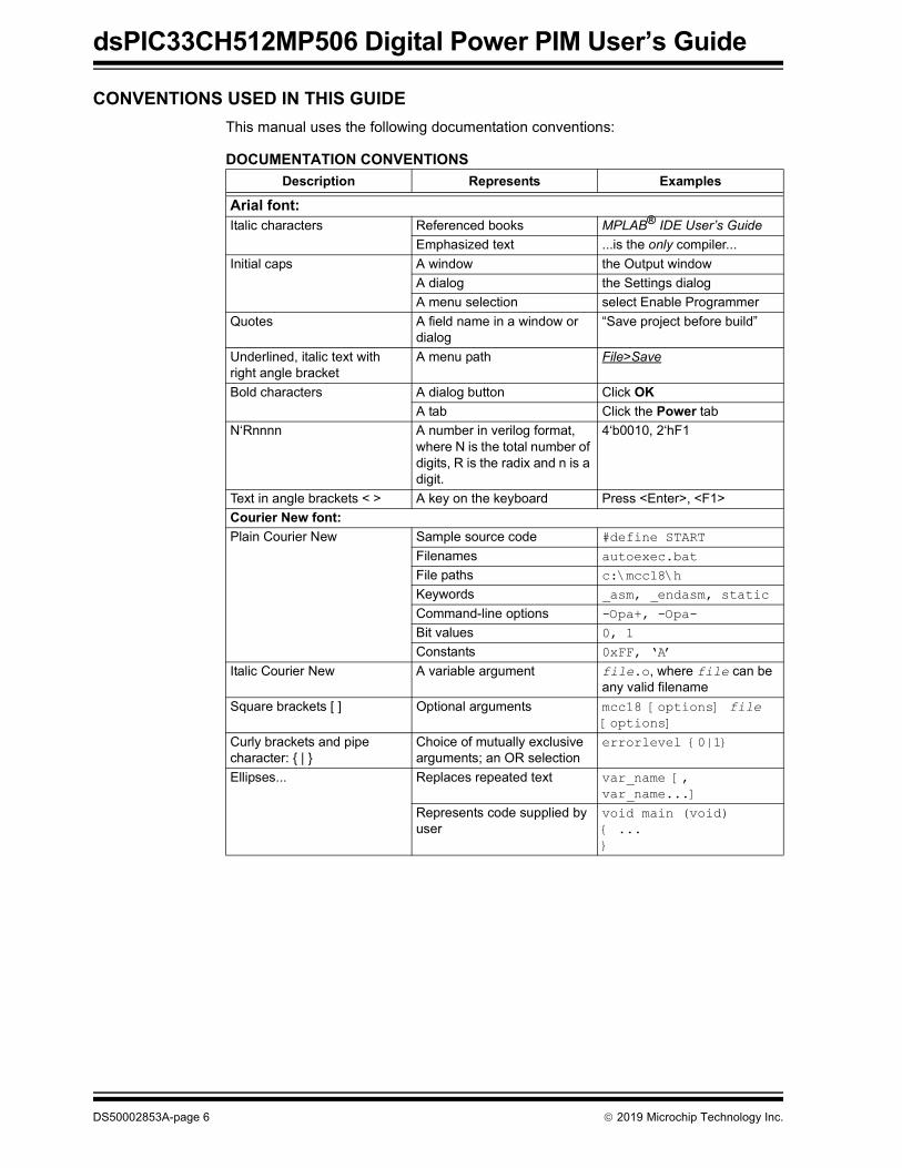
The dsPIC33CH512MP506 DP PIM has the following features, as shown in Figure 1-1.
FIGURE 1-1: dsPIC33CH512MP506 DP PIM
1. Microchip dsPIC33CH512MP506 16-Bit DSC (64-pin TQFP package).
2. ICSP™ programming header for the Master core (6-pin, 2.54 mm header).
3. ICSP programming header for the Slave core (6-pin, 1.27 mm header – not populated).
4. On-board LDO with Power Good (PG) function.
5. Solder pad for ground connection.
6. Micro-USB connector.
7. MCP2221A USB to UART/I2C serial converter.
8. Power indicator LED (Green).
9. User LED (Red).
10. Board edge connection interface for analog inputs/outputs.
11. Board edge connection interface for PWM outputs, digital peripherals and GPIO ports.
Note: Both cores can be programmed and debugged through one ICSP interface.
2019 Microchip Technology Inc. DS50002853A-page 9
dsPIC33CH512MP506 Digital Power PIM User’s Guide
12. Analog input with op amp buffer via test point loop connector; can be used for Bode plot measurements.
13. Op amp buffer for Bode input.
14. Test point loop for DAC output.
15. Test point to access RD13 (also available on card edge connector pin 12).
16. Test point to access RD15 (also available on card edge connector pin 8).
17. Op amp buffers for medium speed ADC inputs.
18. MEMS oscillator.
Board dimensions are: 51 mm (length) x 38.5 mm (width).
1.2.1 Test Points
Table 1-1 lists the test points available on the dsPIC33CH512MP506 DP PIM.
1.2.2 Electrical Characteristics
Table 1-2 shows the electrical characteristics of the dsPIC33CH512MP506 DP PIM.
TABLE 1-1: TEST POINTS
Test Point Name Function/Description
TP1, TP2 Bode Measurement Signal Injection Point
TP3 RB2_DAC1_OUT: Digital-to-Analog Converter Output
TP4 Test Point for Debugging: Access to RD13 through 270 Resistor
TP5 General Purpose Test Point Connected to RD15 along with LD2 (Red LED)
TABLE 1-2: ELECTRICAL CHARACTERISTICS
Parameter Value
Input Voltage Range 3.6 VDC to 10 VDC, Absolute Maximum 16 VDC
Current Consumption Minimum 82 mA, Typical 108 mA, Absolute Maximum 200 mA
Power Dissipation Minimum 295 mW, Typical 414 mW, Maximum 1100 mW
Operating Temperature Range -40°C to +85°C
Note: Typical Test Conditions: Ambient Temperature +25°C, Master core running at 90 MIPS, Slave core running at 100 MIPS, all peripherals powered but not enabled, power-on LED, LD1, active, no USB device or debugger connected.
DS50002853A-page 10 2019 Microchip Technology Inc.
Overview
1.2.3 Analog and Digital Signals
The dsPIC33CH512MP506 DP PIM ensures good signal integrity and provides all signals needed to control a power train. These signals are divided into two main sections: Analog and Digital.
1. Analog SectionThe analog section is located at the short segment of the edge connector. It consists of 17 signals, all referenced to the analog ground. These lines are split into the following subsections:
• High-Speed Comparator Inputs: RC filtered with corner frequency of 10 MHz and maximum signal rise/fall time of 33 ns. These lines are designed to be used with on-chip comparators for signal tracking tasks, such as peak, valley or zero-cross detections.
• High-Speed ADC Inputs: RC filtered with corner frequency of 2 MHz and maximum signal rise/fall time of 180 ns. These lines are connected to the Track-and-Hold (T&H) circuitry of the dedicated ADC inputs and to the Sample-and-Hold (S&H) circuitry of the shared ADC inputs.
• Medium Speed ADC Inputs: Buffered input lines, RC filtered with corner frequency of 1 MHz and maximum signal rise/fall time of 360 ns.
• Low-Speed ADC Inputs: RC filtered with corner frequency of 190 kHz and maximum signal rise/fall time of 1.8 µs.
• 12-Bit DAC Output with Optional On-Board RC Filtering.
2. Digital SectionThe digital section is located at the long segment of the edge connector. It consists of 31 signals, all referenced to digital ground. These lines are split into four subsections:
• High-Speed PWM Outputs: Each line has a 75 series resistance.
• Medium Speed GPIO: Each line has a 270 series resistance.
• Programing/Debugging Lines: Each line has a 100 series resistance.
• Communication Lines (SPI): Each line has a 75 series resistance.
1.2.4 dsPIC33CH512MP506 DP PIM – PCB Edge Connector
The dsPIC33CH512MP506 DP PIM has an edge connector compatible with any application board that provides a mating socket.
The mating socket type is Samtec, Inc.: MECF-30-01-L-DV-WT.
Note: RC filtering and series resistance are needed for good signal integrity, and for reducing EMI issues. Hence, the board can be used for development purposes under frequent plug-in/out cycles. This decoupling also increases robustness in case of accidental shorts and EMC issues.
Note: The range of the digital I/Os allows access to other peripheral functions of the populated DSC, such as communication interfaces like I2C, SPI, UART, Single-Edge Nibble Transmission (SENT), Controller Area Network (CAN), input capture, output compare, Combinatorial Logic Cells (CLC) and more. Please refer to the device data sheet for further information on available functions.
2019 Microchip Technology Inc. DS50002853A-page 11
dsPIC33CH512MP506 Digital Power PIM User’s Guide
1.3 UART COMMUNICATIONThe on-board USB to UART serial bridge enables easy serial connection to PCs. The USB port can provide power to the Digital Power PIM and allows the user to communicate with the dsPIC® Digital Signal Controller (DSC).
The USB driver package and software tool support of the MCP2221A serial converter also offers free terminal software for I2C Master and Slave emulation, as well as generic API drivers for custom software development. Please visit the MCP2221A product web page for more details (www.microchip.com).
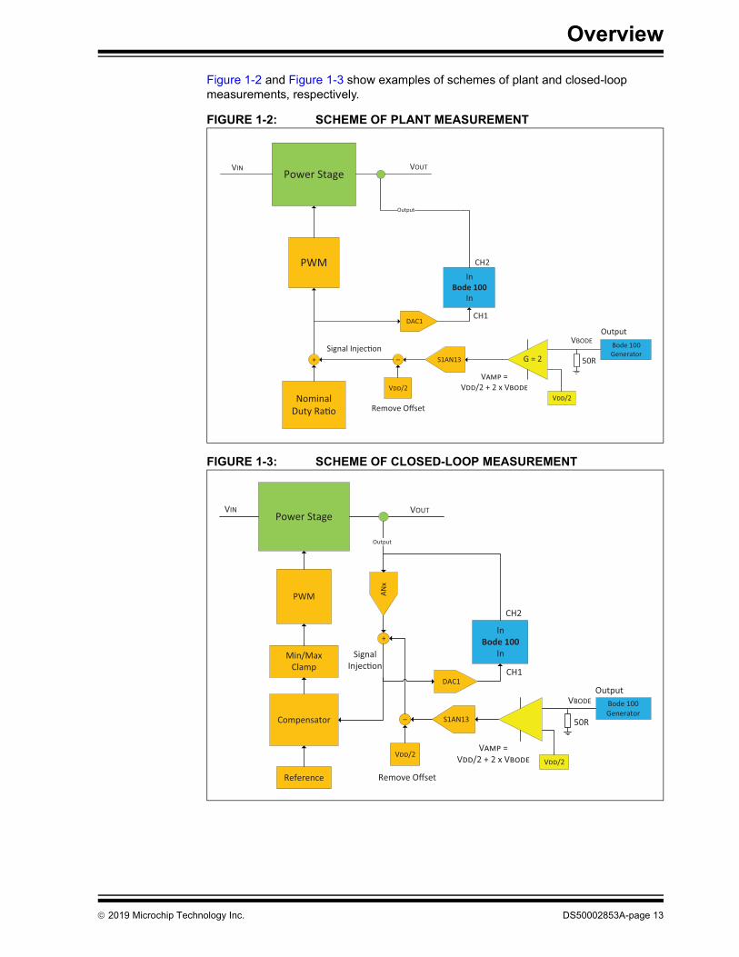
1.4 LOW-FREQUENCY BODE PLOT MEASUREMENTSThe dsPIC33CH512MP506 device, along with an additional on-board circuitry, allows Bode plot measurements to be performed without the need for an isolation transformer. The transformer might still be required if the injected signal tends to be at a very low frequency (for instance, in case of Power Factor Correction (PFC) applications).
Perform the following steps:
1. Solder the 150 resistor from position R74 to R94. Make sure that the RD10_S1AN13_IN line is not driven by any other low-impedance source.
2. Run the power stage in Open-Loop mode with a fixed duty cycle.
3. Connect the Bode 100 AC output to TP1 and TP2. The on-board operational amplifier will add a VDD/2 (1.65V) offset. In this case, no injection transformer is needed.
4. Connect RB2_DAC1_OUT to CH2 of the Bode 100.
5. Use the S1AN13 input to sample the signal from Bode 100 in every PWM cycle at Frequency Switching (fSW) (action in firmware is needed).
6. Remove the VDD/2 offset to regain a signal with no DC value (action in firmware is needed).
7. Add sampled AC signal to the nominal duty cycle (PDCx) (action in firmware is needed).
8. Use a second dedicated ADC core input (ANx) to sample the output of the plant at FSW. The output can be:• Output voltage.• Average coil current sampled at TON/2, where TON is the switch-on time.
9. Duty cycle input and plant output are converted into an analog signal using RB2_DAC1_OUT.
The measured transfer function is the plant (power stage and digital modulator), after scaling and ADC sampling, versus digital duty cycle input (PDCx).
Note: Due to run-time delays of Sample-and-Hold circuits and conversion time of ADC and DAC, this measurement is only recommended for low-frequency measurements: a maximum two decades below sampling frequency.
DS50002853A-page 12 2019 Microchip Technology Inc.
Overview
Figure 1-2 and Figure 1-3 show examples of schemes of plant and closed-loop measurements, respectively.
FIGURE 1-2: SCHEME OF PLANT MEASUREMENT
FIGURE 1-3: SCHEME OF CLOSED-LOOP MEASUREMENT
Power Stage
PWM
VOUTVIN
NominalDuty Ra o
Output
+Signal Injec
S1AN13–
V /2
Remove O set
InBode 100
In
DAC1
Bode 100 Generator
V /2
50R
CH2
CH1
VBODE
G = 2
V =V /2 + 2 x V
Output
Power Stage
PWM
VOUTVIN
Compensator
Output
Bode 100 Generator
InBode 100
In
V /2
Signal Injec n
ANx
–
V /2
Remove O set
Min/Max Clamp
Reference
S1AN13
+
DAC1
50R
CH2
CH1
VBODE
V =V /2 + 2 x V
Output
2019 Microchip Technology Inc. DS50002853A-page 13

dsPIC33CH512MP506 Digital Power PIM User’s Guide
NOTES:
DS50002853A-page 14 2019 Microchip Technology Inc.
dsPIC33CH512MP506 DIGITALPOWER PIM USER’S GUIDE
Appendix A. Board Layout and Schematics
This appendix contains the pinout, the schematics and the board layouts for the dsPIC33CH512MP506 DP PIM.
• Pinout
• Board Schematics
• PCB Layout
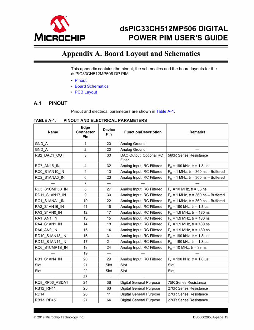
A.1 PINOUT
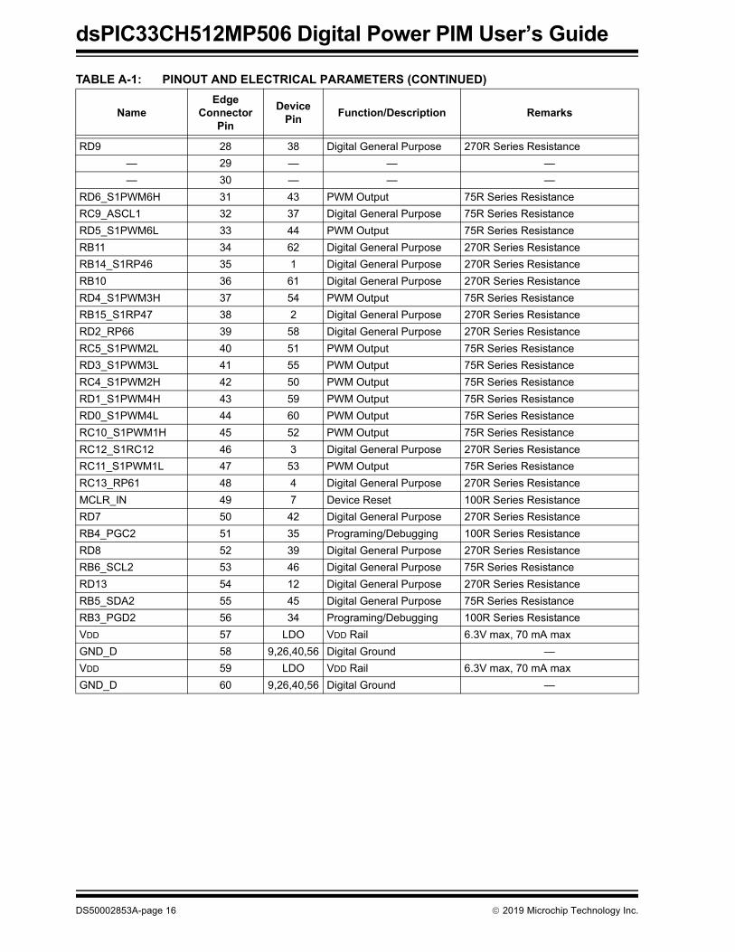
Pinout and electrical parameters are shown in Table A-1.
TABLE A-1: PINOUT AND ELECTRICAL PARAMETERS
NameEdge
Connector Pin
Device Pin
Function/Description Remarks
GND_A 1 20 Analog Ground —
GND_A 2 20 Analog Ground —
RB2_DAC1_OUT 3 33 DAC Output, Optional RC Filter
560R Series Resistance
RC7_AN15_IN 4 32 Analog Input, RC Filtered Fc = 190 kHz, tr = 1.8 µs
RC0_S1AN10_IN 5 13 Analog Input, RC Filtered Fc = 1 MHz, tr = 360 ns – Buffered
RC2_S1ANA0_IN 6 23 Analog Input, RC Filtered Fc = 1 MHz, tr = 360 ns – Buffered
— 7 — — —
RC3_S1CMP3B_IN 8 27 Analog Input, RC Filtered Fc = 10 MHz, tr = 33 ns
RD11_S1AN17_IN 9 30 Analog Input, RC Filtered Fc = 1 MHz, tr = 360 ns – Buffered
RC1_S1ANA1_IN 10 22 Analog Input, RC Filtered Fc = 1 MHz, tr = 360 ns – Buffered
RA2_S1AN16_IN 11 16 Analog Input, RC Filtered Fc = 190 kHz, tr = 1.8 µs
RA3_S1AN0_IN 12 17 Analog Input, RC Filtered Fc = 1.9 MHz, tr = 180 ns
RA1_AN1_IN 13 15 Analog Input, RC Filtered Fc = 1.9 MHz, tr = 180 ns
RA4_S1AN1_IN 14 18 Analog Input, RC Filtered Fc = 1.9 MHz, tr = 180 ns
RA0_AN0_IN 15 14 Analog Input, RC Filtered Fc = 1.9 MHz, tr = 180 ns
RD10_S1AN13_IN 16 31 Analog Input, RC Filtered Fc = 190 kHz, tr = 1.8 µs
RD12_S1AN14_IN 17 21 Analog Input, RC Filtered Fc = 190 kHz, tr = 1.8 µs
RC6_S1CMP1B_IN 18 24 Analog Input, RC Filtered Fc = 10 MHz, tr = 33 ns
— 19 — — —
RB1_S1AN4_IN 20 29 Analog Input, RC Filtered Fc = 190 kHz, tr = 1.8 µs
Slot 21 Slot Slot Slot
Slot 22 Slot Slot Slot
— 23 — — —
RC8_RP56_ASDA1 24 36 Digital General Purpose 75R Series Resistance
RB12_RP44 25 63 Digital General Purpose 270R Series Resistance
RD14 26 11 Digital General Purpose 270R Series Resistance
RB13_RP45 27 64 Digital General Purpose 270R Series Resistance
2019 Microchip Technology Inc. DS50002853A-page 15
dsPIC33CH512MP506 Digital Power PIM User’s Guide
RD9 28 38 Digital General Purpose 270R Series Resistance
— 29 — — —
— 30 — — —
RD6_S1PWM6H 31 43 PWM Output 75R Series Resistance
RC9_ASCL1 32 37 Digital General Purpose 75R Series Resistance
RD5_S1PWM6L 33 44 PWM Output 75R Series Resistance
RB11 34 62 Digital General Purpose 270R Series Resistance
RB14_S1RP46 35 1 Digital General Purpose 270R Series Resistance
RB10 36 61 Digital General Purpose 270R Series Resistance
RD4_S1PWM3H 37 54 PWM Output 75R Series Resistance
RB15_S1RP47 38 2 Digital General Purpose 270R Series Resistance
RD2_RP66 39 58 Digital General Purpose 270R Series Resistance
RC5_S1PWM2L 40 51 PWM Output 75R Series Resistance
RD3_S1PWM3L 41 55 PWM Output 75R Series Resistance
RC4_S1PWM2H 42 50 PWM Output 75R Series Resistance
RD1_S1PWM4H 43 59 PWM Output 75R Series Resistance
RD0_S1PWM4L 44 60 PWM Output 75R Series Resistance
RC10_S1PWM1H 45 52 PWM Output 75R Series Resistance
RC12_S1RC12 46 3 Digital General Purpose 270R Series Resistance
RC11_S1PWM1L 47 53 PWM Output 75R Series Resistance
RC13_RP61 48 4 Digital General Purpose 270R Series Resistance
MCLR_IN 49 7 Device Reset 100R Series Resistance
RD7 50 42 Digital General Purpose 270R Series Resistance
RB4_PGC2 51 35 Programing/Debugging 100R Series Resistance
RD8 52 39 Digital General Purpose 270R Series Resistance
RB6_SCL2 53 46 Digital General Purpose 75R Series Resistance
RD13 54 12 Digital General Purpose 270R Series Resistance
RB5_SDA2 55 45 Digital General Purpose 75R Series Resistance
RB3_PGD2 56 34 Programing/Debugging 100R Series Resistance
VDD 57 LDO VDD Rail 6.3V max, 70 mA max
GND_D 58 9,26,40,56 Digital Ground —
VDD 59 LDO VDD Rail 6.3V max, 70 mA max
GND_D 60 9,26,40,56 Digital Ground —
TABLE A-1: PINOUT AND ELECTRICAL PARAMETERS (CONTINUED)
NameEdge
Connector Pin
Device Pin
Function/Description Remarks
DS50002853A-page 16 2019 Microchip Technology Inc.
Bo
ard L
ayou
t and
Sch
ematics
2
01
9 M
icroch
ip T
ech
no
log
y Inc.
DS
50
00
28
53
A-p
ag
e 1
7
A.
FIG
Designed with
Altium.com
1k04021%
R76
+3.3V_OPA
GND_A
0.1 μF50V0402
C20
GND_A
VIN-3
VIN+1
VOUT4
Vss
2
VDD
5
MCP6V91UTU5
RC0_S1AN10_IN
RC2_S1ANA0_IN
RC1_S1ANA1_IN
OPA_1
+3.3V_OPA
1k04021%
R77
+3.3V_OPA
GND_A
0.1 μF50V0402
C21
GND_A
VIN-3
VIN+1
VOUT4
Vss
2
VDD
5
MCP6V91UTU6
OPA_2
+3.3V_OPA
1k04021%
R78
+3.3V_OPA
GND_A
0.1 μF50V0402
C22
GND_A
VIN-3
VIN+1
VOUT4
Vss
2
VDD
5
MCP6V91UTU7
OPA_3
+3.3V_OPA
+3.3V_OPA
GND_A
0.1 μF50V0402
C23
GND_A
VIN-3
VIN+1
VOUT4
Vss
2
VDD
5
MCP6V91UTU8
OPA_4
+3.3V_OPA
1k04021%
R79
OPA_1_IN
OPA_2_IN
OPA_3_IN
OPA_4_IN
RD11_S1AN17_IN
10k04020.5%
R95
49.9R08051%
R90
GND_A
Vbode_max = 1 Vrms
TP LOOP Yellow
TP2
VBODE
TP LOOP Black
TP1
49.9R0603 1%R93
GND_A
10k0402 0.5%R92
0.1 μF50V0402
C51
GND_A
10k0402 0.5%R91
3.3k04020.5%
R96
VIN-3
VIN+1
VOUT4
Vss
2
VDD
5
MCP6V91UTU4
+3.3V_OPA
+3.3V_OPA
GND_A
0.1 μF50V0402
C24
GND_A
+3.3V_OPA
VB_inj = Vcc/2 – VBODE
22pF50V0402
C50
Bode_Inj
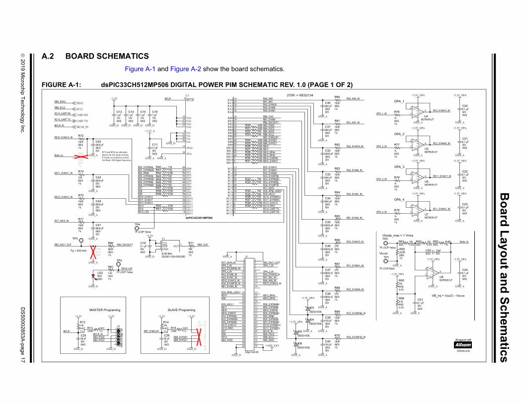
2 BOARD SCHEMATICS
Figure A-1 and Figure A-2 show the board schematics.
URE A-1: dsPIC33CH512MP506 DIGITAL POWER PIM SCHEMATIC REV. 1.0 (PAGE 1 OF 2)
5600 pF060325V
C37
560 pF060350V
C34
560 pF060350V
C33
+3.3V
0.1uF50V0402
C17
GND_DGND_DGND_D
GND_D
GND_A GND_A
GND_A
GND_A
GND_A
GND_A
GND_A
5600 pF060325V
C32
GND_A
100 pF060350V
C39
GND_A
GND_D
75RR37
TP3
75RR36
75RR4475RR43
75RR3275RR33
75RR46
GND_A
GND_D
75RR35
270RR50270RR51
75RR34
5600 pF060325V
C36
GND_A
GND_A
5600 pF060325V
C41
GND_A
100 pF060350V
C40
GND_A
GND_A
560 pF060350V
C30
Fg = 500 kHz
GND_D
100RR20100RR21
dsPIC33CH512MP506
VDD57 VDD41 VDD25 VDD10
VSS40 VSS26 VSS
9
RD060
RD159
RD258
RD355
RD454
RD544
RD643
RD742
RD839
RD938
RD1031
RD1130
RD1221
RD1312
RD1411
RD158
MCLR7
VSS56
AVDD19
AVSS20
RA0 14
RA1 15
RA2 16
RA3 17
RA4 18
RB0 28
RB1 29
RB2 33
RB3 34
RB4 35
RB5 45
RB6 46
RB7 47
RB8 48
RB9 49
RC0 13
RC1 22
RC2 23
RC3 27
RC4 50
RC5 51
RC6 24
RC7 32
RC8 36
RC9 37
RC10 52
RC11 53
RC12 3
RC13 4
RC14 5
RC15 6
RB10 61
RB11 62
RB12 63
RB13 64
RB14 1
RB15 2
U3
560 pF060350V
C31
GND_A
GND_A
75RR45
100RR25100RR24
75RR2275RR23
270RR49270RR48
5600 pF060325V
C38
GND_A
75RR4175RR40
RED0603
LD2
1234567891011121314151617181920
2324252627282930313233343536373839404142434445464748495051525354555657585960
Edge Card 60
J5
RB0_CLKI
RB2_DAC1_OUT
RB2_DAC1_OUT RB2_DACOUT1
RB2_DACOUT1RB3_PGD2RB4_PGC2
+3.3V_A
OPA_1_IN
RB3_PGD2
MCLR_INRB4_PGC2RB6_SCL2RB5_SDA2
RC7_AN15_IN
RA3_S1AN0_IN
RD10_S1AN13_IN
RC8_RP56_ASDA1
RC2_S1ANA0
RC1_S1ANA1_IN
RC0_S1AN10_IN
RC7_AN15_IN
RD11_S1AN17_IN
RD15_LEDOPA_2_IN
OPA_3_INOPA_4_IN
150R06031%
R75
150R06031%
R60
150R06031%
R63
150R06031%
R64
150R06031%
R71
150R06031%
R61
150R06031%
R62
150R06031%
R69
150R06031%
R70
5600 pF25V0603
C43
5600 pF25V0603
C44
150R06031%
R72
27R06031%
R67
27R06031%
R68
27R06031%
R66
27R06031%
R74
1 μF10V0402
C131 μF10V0402
C141 μF10V0402
C151 μF10V0402
C16
MCLR
+3.3V
MASTER Programing
GND_D
123456
HDR-
2.54 M
ale 1
x6
J1
RB3_PGD2RB4_PGC2
MCLR
+3.3V
GND_D
100R04021%
R1310k04021%
R12
56 pF50V0402
C25
MCLR_IN MCLR_IN
SDA2
SCL2
UART TX
UART RX
RC14_UART TX
RC15_UART RX
+3.3V
SLAVE Programing
GND_D
+3.3V
GND_D
123456
HD
R-1
.27
Mal
e 1x
6 ST
AG
DNPJ2
10k04021%
R14
100R04021%
R15RB7_S1MCLR1
RB8_S1PGD1RB9_S1PGC1
MCLR_IN
RC7_AN15
RC0_S1AN10
RC3_S1CMP3B_IN
RC3_S1CMP3B_IN
RC3_S1CMP3B
RC1_S1ANA1
RC2_S1ANA0_IN
RA2_S1AN16_IN
RA2_S1AN16_IN
RA2_S1AN16
RA3_S1AN0_IN
RA3_S1AN0
RA1_AN1
RA1_AN1_IN
RA1_AN1_INRA4_S1AN1_IN
RA4_S1AN1_IN
RA4_S1AN1
RA0_AN0_IN
RA0_AN0_INRA0_AN0
RD10_S1AN13_IN
RD12_S1AN14_IN
RD12_S1AN14_IN
RC6_S1CMP1B
RC6_S1CMP1B_IN
RC6_S1CMP1B_INRB1_S1AN4_IN
RB1_S1AN4
5600 pF060325V
C35
GND_A
150R06031%
R65 RB1_S1AN4_IN
RD10_S1AN13RD11_S1AN17RD12_S1AN14
5600 pF060325V
C42
RC8_RP56_ASDA1
RB12_RP44
RB12_RP44
RD14
RD14
RB13_RP45
RB13_RP45
RD9
RD9
RD6_S1PWM6H
RD6_S1PWM6H
RD5_S1PWM6L
RD5_S1PWM6L
RC9_ASCL1
RC9_ASCL1
RB11RB14_S1RP46
RB14_S1RP46
RB10
RB10RB11
RD4_S1PWM3H
RD4_S1PWM3HRD3_S1PWM3L
RD3_S1PWM3L
RB15_S1RP47
RB15_S1RP47
RD2_RP66
RD2_RP66
RC5_S1PWM2L
RC5_S1PWM2LRC4_S1PWM2H
RC4_S1PWM2HRD1_S1PWM4H
RD1_S1PWM4HRD0_S1PWM4L
RD0_S1PWM4LRC10_S1PWM1H
RC10_S1PWM1HRC11_S1PWM1L
RC11_S1PWM1LRC12_S1RC12
RC12_S1RC12
RC13_RP61
RC13_RP61
RD7
RD7
RD8
RD8
RB6_SCL2RB5_SDA2
RB6_SCL2
RB5_SDA2
RD13
RD13
RC15_UART RXRC14_UART TX
RD15_LED
RB7_S1MCLR1RB8_S1PGD1RB9_S1PGC1
270RR42
270RR47
270RR26270RR27270RR28270RR29270RR30270RR31
270RR38270RR39
0.1 μF50V0402
C18
GND_D
+3.3V
75R04021%
R11 RB0_CLKISTB1
GND2 OUT 3VDD4
8.000 MHzDSC6011JI2A-008.0000
Y1
0603DNP
C45 560R06031%
R80
GND_A
GND_A
+3.3V_OPA
+3.3V_OPA
150R06031%
DNPR94Bode_Inj
56 pF50V0402
C26
R72 and R94 are alternateplaces for the same resistor.It forms an isolation switch for Bode 100 Signal Injection.
DB2S31000LD4
DB2S31000LD3
DB2S31000LD6
DB2S31000LD5
+VDD_EXT
3.3k04021%
R81
270R -> RES2134
TP LOOP Yellow
TP4
TP LOOP Yellow
TP5
dsP
IC33C
H512M
P506 D
igital P
ow
er PIM
User’s G
uid
e
DS
50
00
28
53
A-p
ag
e 1
8
20
19
Micro
chip
Te
chn
olo
gy In
c.
Designed with
Altium.com
SDA2
SCL2
UART TX
UART RX
3.3V
ND_D
+3.3V_A
GND_A
+3.3V_OPA3.3V
GND_A
10 μF10V0603
C1010 μF10V0603
C11
10 μF10V0603
C12
600R0402900 mA
FB6
600R0402900 mA
FB7
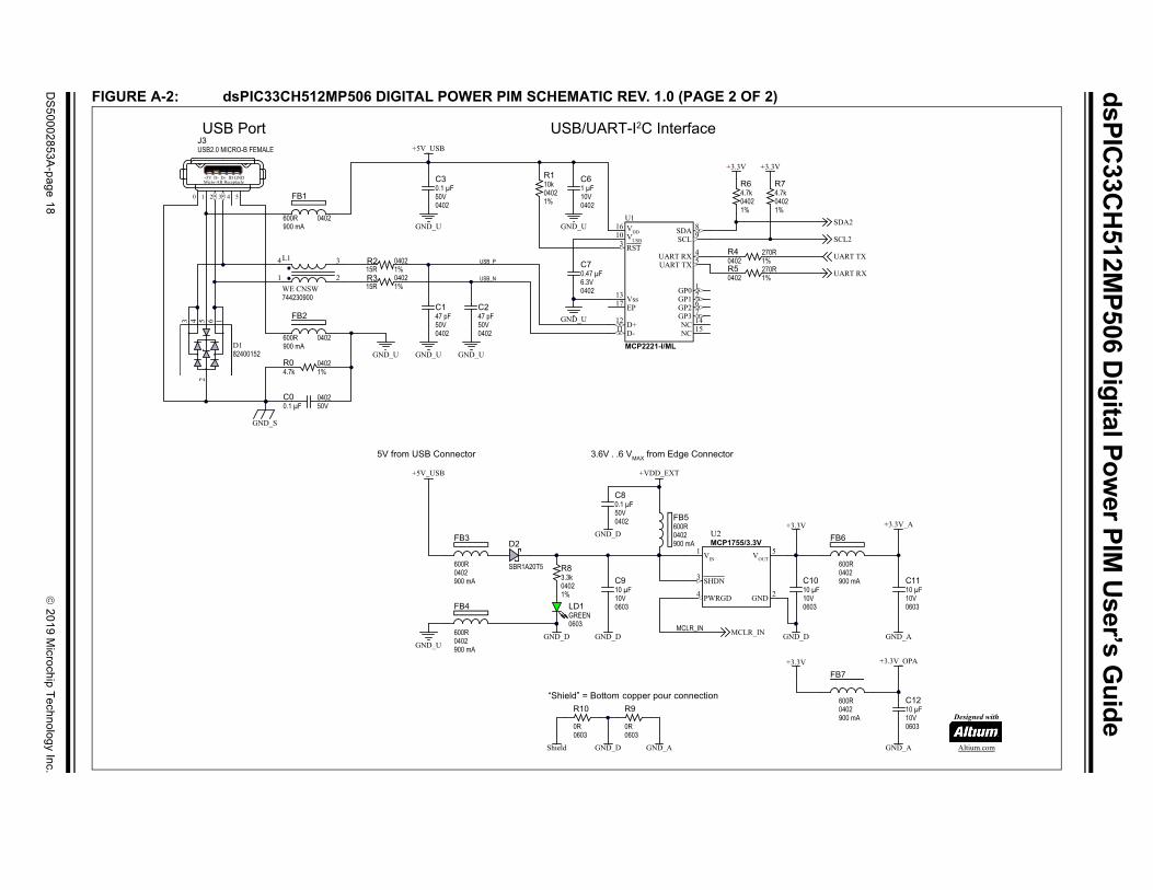
FIGURE A-2: dsPIC33CH512MP506 DIGITAL POWER PIM SCHEMATIC REV. 1.0 (PAGE 2 OF 2)
10k04021%
R1
270R0402 1%R4
270R0402 1%R5
+3.3V +3.3V
VDD16
GP0 1
GP1 2
RST3
UART RX 4
UART TX 5
GP2 6
GP3 7
SDA 8
SCL 9VUSB10
D-11 D+12
Vss13
EP17
NC 14
NC 15
MCP2221-I/ML
U1
4.7k04021%
R64.7k04021%
R7
GND_D
+VDD_EXT
+
GGND_D
3.6V . .6 VMAX from Edge Connector
+5V_USB
0.1 μF50V0402
C8
GND_D
3.3k04021%
R8
GREEN0603
LD1
VIN1
SHDN3
GND 2PWRGD4
VOUT5
MCP1755/3.3VU2
MCLR_IN MCLR_IN
GND_A
0R0603
R9
GND_D
0R0603
R10
Shield
“Shield” = Bottom copper pour connection
+
1 μF10V0402
C6
0.47 μF6.3V0402
C7
10 μF10V0603
C9
600R0402900 mA
FB3600R0402900 mA
FB5
GND_U
GND_U
SBR1A20T5
D2
1 2 3 4 50
DNGV5+ -D +D DIMicro-AB Receptacle
USB2.0 MICRO-B FEMALEJ3
GND_S
+5V_USB
USB_N
USB_P3
1
4
2
744230900
L1
WE CNSW
1
2
3 4 5 6
82400152D1
GND_U
USB Port
0.1 μF50V0402
C3
47 pF50V0402
C147 pF50V0402
C2
GND_U GND_UGND_U
GND_U
600R0402900 mA
FB4
USB/UART-I2C Interface
600R 0402900 mA
FB1
600R 0402900 mA
FB2
4.7k04021%
R0
15R04021%
R2
15R04021%
R3
0.1 μF 50V0402C0
5V from USB Connector
Board Layout and Schematics
A.3 PCB LAYOUT
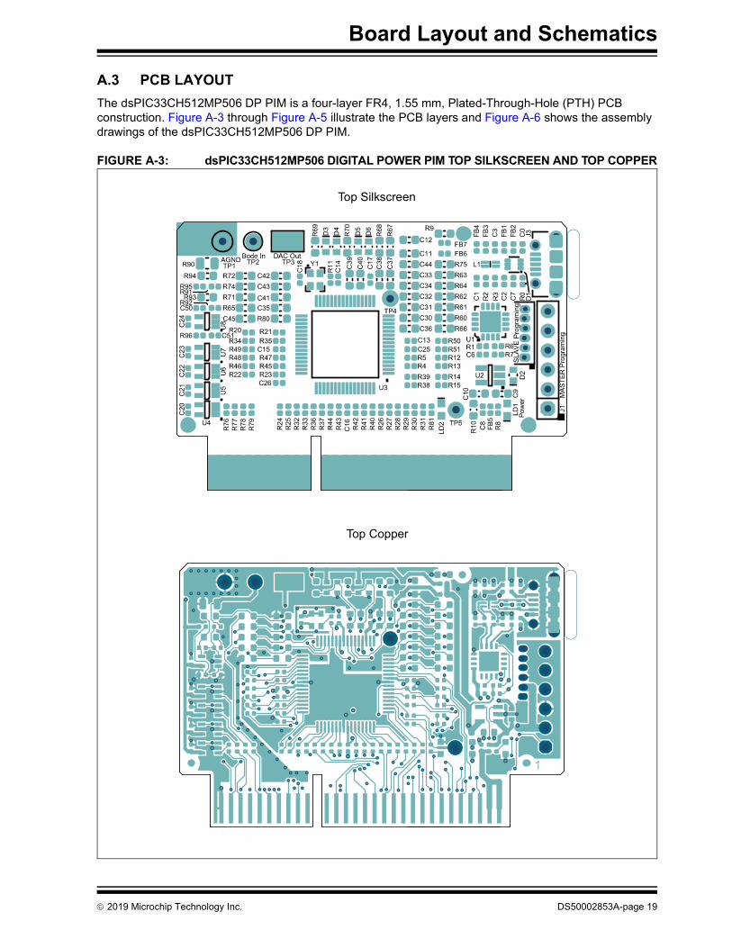
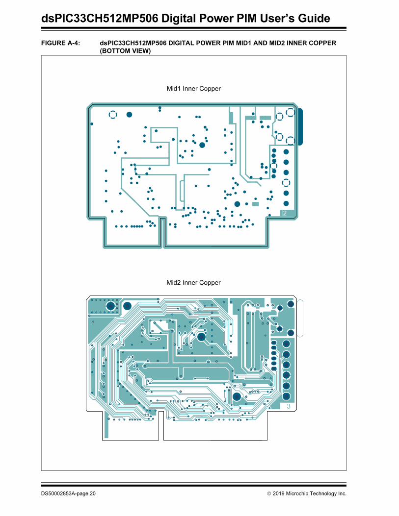
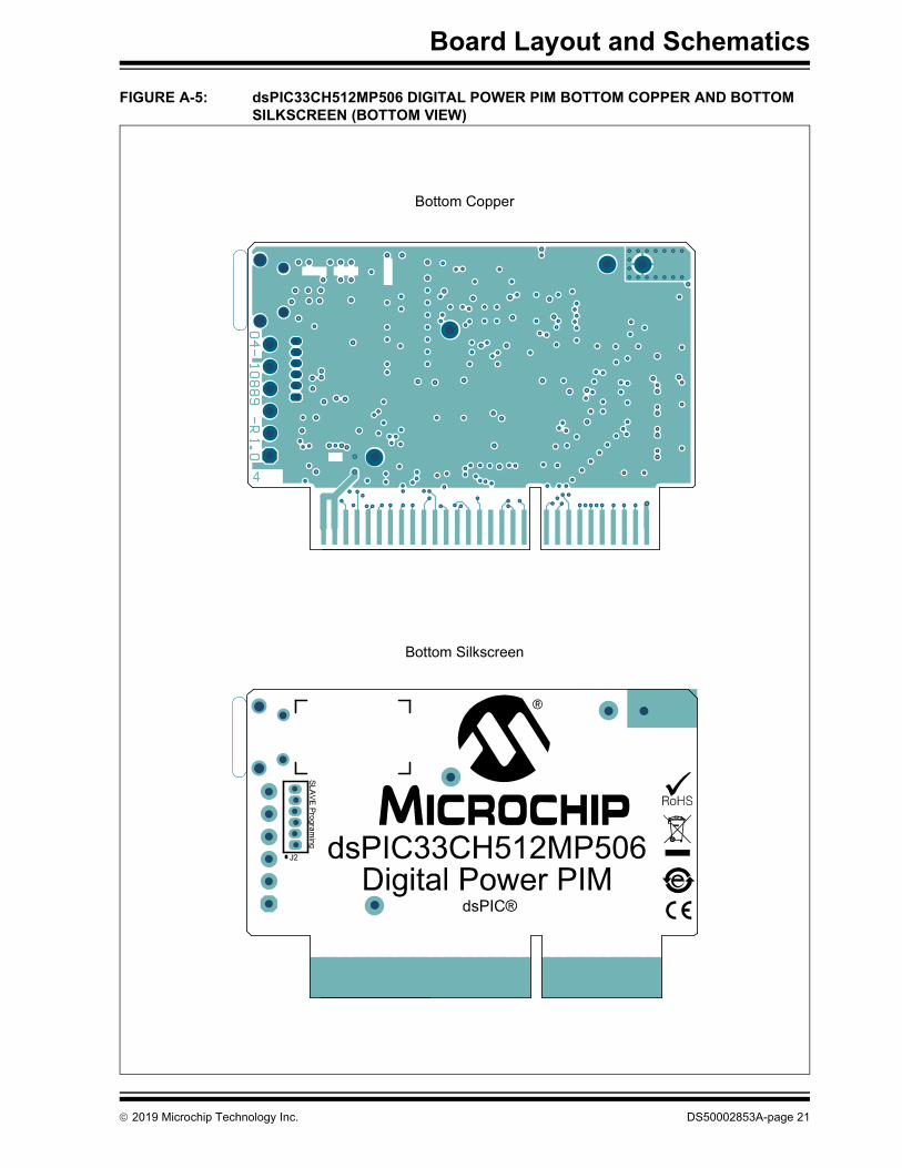
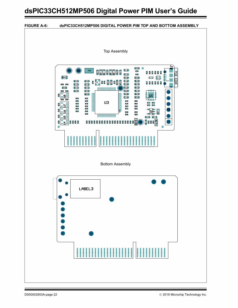
The dsPIC33CH512MP506 DP PIM is a four-layer FR4, 1.55 mm, Plated-Through-Hole (PTH) PCB construction. Figure A-3 through Figure A-5 illustrate the PCB layers and Figure A-6 shows the assembly drawings of the dsPIC33CH512MP506 DP PIM.
FIGURE A-3: dsPIC33CH512MP506 DIGITAL POWER PIM TOP SILKSCREEN AND TOP COPPER
Top Silkscreen
Top Copper
2019 Microchip Technology Inc. DS50002853A-page 19
dsPIC33CH512MP506 Digital Power PIM User’s Guide
FIGURE A-4: dsPIC33CH512MP506 DIGITAL POWER PIM MID1 AND MID2 INNER COPPER (BOTTOM VIEW)
Mid1 Inner Copper
Mid2 Inner Copper
DS50002853A-page 20 2019 Microchip Technology Inc.
Board Layout and Schematics
FIGURE A-5: dsPIC33CH512MP506 DIGITAL POWER PIM BOTTOM COPPER AND BOTTOM SILKSCREEN (BOTTOM VIEW)
Bottom Copper
Bottom Silkscreen
2019 Microchip Technology Inc. DS50002853A-page 21
dsPIC33CH512MP506 Digital Power PIM User’s Guide
FIGURE A-6: dsPIC33CH512MP506 DIGITAL POWER PIM TOP AND BOTTOM ASSEMBLY
Top Assembly
Bottom Assembly
1
5
0
0
1
1
1
2
3
4
0
0
6
1
1
2
1
1
2
2
1
2
2
3
2
1
2
1
1
3
3
2
1
3
1
1
2
1
2
2 1
21
1 2
21
12
2
2
2
1
12
21
21
21
12
1
2
2
1
2
32
2
1
2
1
2
30 29 28
2
1
2
2
11
2
26 25 24
2
1
2
22 21 20
2
1
2
2
1
18 17
1
2
1
1
5
4
3
9
8
7
13
12
11
16
15
2
1
2
1
2
1
1
1
1
2
2
2
2
2
2
1
2 1
2
1
2
1
2
2
1
1
1
2
1
1
2
2
2
1
2
2
1
1
12
2
3
2
1
2
1
1
2
12
2
4
1
1
2
2
1
2
1
1
2
1
1
1
1
3
2
2
2
1
5 7
12
2
2
11 13
12
12
17
1
49
1
23
535251
1
27
575655
1
29
616059
1
33
6463
2
37
14
10
6
2
1
39
1
2
2
2
2
43 45
1
2
1
2
1
2
49
2
1
2
1
53 55
5
2 1
21
4
12 11
1
2
59
1
43
12
3
10 9
1
2
1
1
2
4
5
5
5
4
4
2 1
5
4
1
1 2
1
2
1
2
1
1 1
21
2
1 1
2
1
2
48
46
45
44
42
41
40
38
37
36
2 34
33
2
31 27
1 3
1
2
2
1 2
1
2
1
23 19
1 2
1 11
2 22
1
2
22
1
2
2
2
2 1
1
1
1
1
1
1
2
1
22
16 5
14
13 8
7
122
6
25
1
11 1
3
2
1
5
5
4
2 2
93
11
11
251915
5450
47
43
39
35
24
2
3531
6258
2 1
514741
2 2
1
2
1 1
1
1
1
57
1
2 1
2
15 6
2
34
11
22 2
0
4
0
0
17
0
2
1
1
5
0
0
1
1
1
2
3
4
0
0
6
1
268121418242830343840444650545660 10 426 20 1636 3252 48 4258
DS50002853A-page 22 2019 Microchip Technology Inc.
dsPIC33CH512MP506 DIGITALPOWER PIM USER’S GUIDE
Appendix B. Bill of Materials (BOM)
This appendix contains the Bill of Materials (BOM) for the dsPIC33CH512MP506 Digital Power PIM.
• Bill of Materials
B.1 BILL OF MATERIALS
Table B-1 shows the Bill of Materials for the dsPIC33CH512MP506.
TABLE B-1: dsPIC33CH512MP506 DIGITAL POWER PIM BILL OF MATERIALS (BOM)
Qty Designator Description Manufacturer Manufacturer Part Number
11 C0, C3, C8, C17, C18, C20, C21, C22, C23, C24, C51
Capacitor, Ceramic, 0.1 µF, 50V, 10%, X7R, SMD, 0402
TDK Corporation C1005X7R1H104K050BB
2 C1, C2 Capacitor, Ceramic, 47 pF, 50V, 5%, NP0, SMD, 0402
Murata Electronics® GRM1555C1H470JA01D
5 C6, C13, C14, C15, C16 Capacitor, Ceramic, 1 µF, 10V, 10%, X7S, SMD, 0402
TDK Corporation C1005X7S1A105K050BC
1 C7 Capacitor, Ceramic, 0.47 µF, 6.3V, 10%, X5R, SMD, 0402
Murata Electronics GRM155R60J474KE19D
4 C9, C10, C11, C12 Capacitor, Ceramic, 10 µF, 10V, 20%, X5R, SMD, 0603
Samsung Group CL10A106MP8NNNC
2 C25, C26 Capacitor, Ceramic, 56 pF, 50V, 5%, C0G, SMD, 0402
TDK Corporation C1005C0G1H560J050BA
4 C30, C31, C33, C34 Capacitor, Ceramic, 560 pF, 50V, 5%, C0G, NP0, SMD, 0603
KEMET C0603C561J5GACTU
9 C32, C35, C36, C37, C38, C41, C42, C43, C44
Capacitor, Ceramic, 5600 pF, 25V, 5%, C0G, SMD, 0603
TDK Corporation C1608C0G1E562J080AA
2 C39, C40 Capacitor, Ceramic, 100 pF, 50V, 5%, NP0, SMD, 0603
AVX Corporation GMC10CG101J50NT
1 C50 Capacitor, HiQ, 22 pF, 50V, 5%, NP0, 1.95 GHz, SMD, 0402
Johanson Technology Inc.
500R07S220JV4T
1 D1 Diode, TVS Array, 82400152, 5V, USB 2.0, SMD, SOT-563
Wurth Elektronik 82400152
1 D2 Diode, Schottky, SBR1A20T5-7, 520 mV, 1A, 20V, SOD-523
Diodes Incorporated® SBR1A20T5-7
4 D3, D4, D5, D6 Diode, Schottky, DB2S31000L, 470 mV, 200 mA, 30V, SMD, SOD-523
Panasonic® - ECG DB2S31000L
7 FB1, FB2, FB3, FB4, FB5, FB6, FB7
Ferrite, 600R at 100 MHz, 0.23R, 900 mA, SMD, 0402
Murata Electronics BLM15PX601SN1D
1 J1 Connector Header-2.54, Male, 1x6 Gold, 5.84 MH TH, Vertical
FCI 68000-106HLF
1 J3 Connector, USB 2.0, Micro-B, Female, TH/SMD, R/A
FCI 10118194-0001LF
2019 Microchip Technology Inc. DS50002853A-page 23
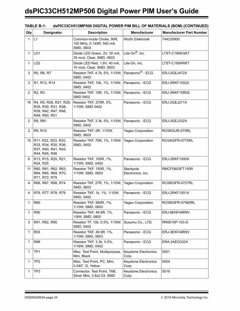
dsPIC33CH512MP506 Digital Power PIM User’s Guide
1 L1 Common-mode Choke, 90R, 100 MHz, 0.145R, 550 mA, SMD, 0603
Wurth Elektronik 744230900
1 LD1 Diode LED Green, 2V, 30 mA, 35 mcd, Clear, SMD, 0603
Lite-On®, Inc. LTST-C190KGKT
1 LD2 Diode LED Red, 1.8V, 40 mA, 10 mcd, Clear, SMD, 0603
Lite-On, Inc. LTST-C190KRKT
3 R0, R6, R7 Resistor TKF, 4.7k, 5%, 1/10W, SMD, 0402
Panasonic® - ECG ERJ-2GEJ472X
3 R1, R12, R14 Resistor TKF, 10k, 1%, 1/10W, SMD, 0402
Panasonic - ECG ERJ-2RKF1002X
2 R2, R3 Resistor TKF, 15R, 1%, 1/10W, SMD 0402
Panasonic - ECG ERJ-2RKF15R0X
16 R4, R5, R26, R27, R28, R29, R30, R31, R38, R39, R42, R47, R48, R49, R50, R51
Resistor TKF, 270R, 5%, 1/10W, SMD 0402
Panasonic - ECG ERJ-2GEJ271X
2 R8, R81 Resistor TKF, 3.3k, 5%, 1/10W, SMD, 0402
Panasonic - ECG ERJ-2GEJ332X
2 R9, R10 Resistor TKF, 0R, 1/10W, SMD, 0603
Yageo Corporation RC0603JR-070RL
15 R11, R22, R23, R32, R33, R34, R35, R36, R37, R40, R41, R43, R44, R45, R46
Resistor TKF, 75R, 1%, 1/16W, SMD, 0402
Yageo Corporation RC0402FR-0775RL
6 R13, R15, R20, R21, R24, R25
Resistor TKF, 100R, 1%, 1/10W, SMD, 0402
Panasonic - ECG ERJ-2RKF1000X
11 R60, R61, R62, R63, R64, R65, R69, R70, R71, R72, R75
Resistor TKF, 150R, 1%, 1/10W, SMD, 0603
Stackpole Electronics, Inc.
RMCF0603FT150R
4 R66, R67, R68, R74 Resistor TKF, 27R, 1%, 1/10W, SMD, 0603
Yageo Corporation RC0603FR-0727RL
4 R76, R77, R78, R79 Resistor TKF, 1k, 1%, 1/10W, SMD, 0402
Panasonic - ECG ERJ-2RKF1001X
1 R80 Resistor TKF, 560R, 1%, 1/10W, SMD, 0603
Yageo Corporation RC0603FR-07560RL
1 R90 Resistor TKF, 49.9R, 1%, 1/8W, SMD, 0805
Panasonic - ECG ERJ-6ENF49R9V
3 R91, R92, R95 Resistor TF, 10k, 0.5%, 1/16W, SMD, 0402
Susumu Co., LTD. RR0510P-103-D
1 R93 Resistor TKF, 49.9R, 1%, 1/10W, SMD, 0603
Panasonic - ECG ERJ-3EKF49R9V
1 R96 Resistor TKF, 3.3k, 0.5%, 1/16W, SMD, 0402
Panasonic - ECG ERA-2AED332X
1 TP1 Misc. Test Point, Multipurpose, Mini, Black
Keystone Electronics Corp.
5001
1 TP2 Misc. Test Point, PC, Mini,0.040", D, Yellow
Keystone Electronics Corp.
5004
1 TP3 Connector, Test Point, TAB, Silver Mini, 3.8x2.03, SMD
Keystone Electronics Corp.
5019
TABLE B-1: dsPIC33CH512MP506 DIGITAL POWER PIM BILL OF MATERIALS (BOM) (CONTINUED)
Qty Designator Description Manufacturer Manufacturer Part Number
DS50002853A-page 24 2019 Microchip Technology Inc.
Bill of Materials (BOM)
2 TP4, TP5 Misc. Test Point, PC, Mini,0.040", D, Yellow
Keystone Electronics Corp.
5004
1 U1 Microchip Interface, USB,I2C/UART, MCP2221A-I/ML,QFN-16
Microchip Technology Inc.
MCP2221A-I/ML
1 U2 Microchip Analog LDO, 3.3V,MCP1755T-3302E/OT,SOT-23-5
Microchip Technology Inc.
MCP1755T-3302E/OT
1 U3 Microchip MCU, 16-Bit, 180/200 MHz, 512/72 kB, 48/16 kB, dsPIC33CH512MP506-I/PT, TQFP-64
Microchip Technology Inc.
dsPIC33CH512MP506-I/PT
5 U4, U5, U6, U7, U8 Microchip Analog Op Amp,1-Ch, 10 MHz, MCP6V91UT-E/LTYCT-ND, SC-70-5
Microchip Technology Inc.
MCP6V91UT-E/LTY
1 Y1 Microchip Clock Oscillator,Single, 8.000 MHz, DSC6011JI2A-008.0000, VDFN-4
Microchip Technology Inc.
DSC6011JI2A-008.0000
TABLE B-1: dsPIC33CH512MP506 DIGITAL POWER PIM BILL OF MATERIALS (BOM) (CONTINUED)
Qty Designator Description Manufacturer Manufacturer Part Number
2019 Microchip Technology Inc. DS50002853A-page 25

dsPIC33CH512MP506 Digital Power PIM User’s Guide
NOTES:
DS50002853A-page 26 2019 Microchip Technology Inc.
dsPIC33CH512MP506 DIGITALPOWER PIM USER’S GUIDE
Appendix C. Characterization Data
This chapter provides some characterization data and further guidance on sub-circuits of this Digital Power PIM to allow engineers to gain a better understanding of technical limitations, as well as enable users to solve design trade-offs in additional circuits on custom boards, such as signal conditioning or auxiliary power supplies.
C.1 MEASUREMENT ACCURACY IMPACTS
C.1.1 High-Speed Analog Signal Tracking Considerations
Each of the four groups of the analog inputs, high-speed ADC, mid-speed ADC, low-speed ADC and high-speed comparator inputs have been equipped with RC low-pass filters to prevent corruption of sampling results, such as alias-frequencies being injected into a series of ADC sampling results, and to ensure proper operation of the high-speed comparators in noisy environments. These deliberate bandwidth limitations, however, may affect the accuracy of the ADC results when tracking high-speed signals.
C.1.1.1 FILTER BANDWIDTH IMPACTS
This section discusses the influence of the RC low-pass filter bandwidth limits versus the expected sampling error to allow designers to identify the maximum signal slew rate, which can be tracked with a certain known accuracy.
The cutoff frequency, fc, of an RC low-pass filter defines the frequency at which its output signal magnitude is reduced by -3dB.
The first-order RC filter cutoff frequency is defined by Equation C-1.
EQUATION C-1:
When using high-speed ADCs with sampling times of 10 ns to 50 ns or less, tracking signal transients at this frequency will also show a 3 dB offset in ADC results in accordance to the damped signal gain. To allow a more accurate analysis of the tracking error, with regards to the transient frequency, we need to look at the total gain characteristic over frequency.
Note: The graphs and tables provided following this note are a statistical summary based on a limited number of samples and are provided for informational purposes only. The performance characteristics listed herein are not tested or guaranteed. In some graphs or tables, the data presented may be outside the specified operating range (e.g., outside specified power supply range), and therefore, outside the warranted range.
fc1
2 RFiltCFilt ----------------------------------=
2019 Microchip Technology Inc. DS50002853A-page 27
dsPIC33CH512MP506 Digital Power PIM User’s Guide
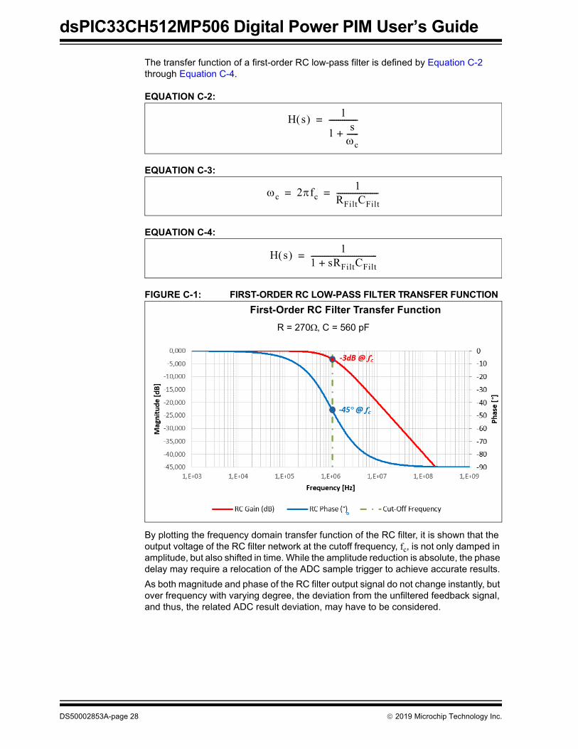
The transfer function of a first-order RC low-pass filter is defined by Equation C-2 through Equation C-4.
EQUATION C-2:
EQUATION C-3:
EQUATION C-4:
FIGURE C-1: FIRST-ORDER RC LOW-PASS FILTER TRANSFER FUNCTION
By plotting the frequency domain transfer function of the RC filter, it is shown that the output voltage of the RC filter network at the cutoff frequency, fc, is not only damped in amplitude, but also shifted in time. While the amplitude reduction is absolute, the phase delay may require a relocation of the ADC sample trigger to achieve accurate results.
As both magnitude and phase of the RC filter output signal do not change instantly, but over frequency with varying degree, the deviation from the unfiltered feedback signal, and thus, the related ADC result deviation, may have to be considered.
H s 1
1sc------+
---------------=
c 2fc1
RFiltCFilt----------------------= =
H s 11 sRFiltCFilt+-----------------------------------=
First-Order RC Filter Transfer Function
R = 270, C = 560 pF
DS50002853A-page 28 2019 Microchip Technology Inc.
Characterization Data
C.1.2 Example
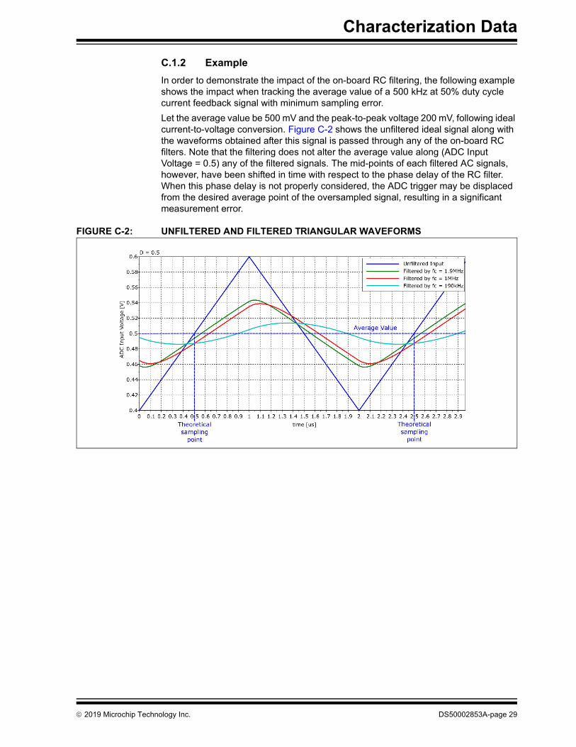
In order to demonstrate the impact of the on-board RC filtering, the following example shows the impact when tracking the average value of a 500 kHz at 50% duty cycle current feedback signal with minimum sampling error.
Let the average value be 500 mV and the peak-to-peak voltage 200 mV, following ideal current-to-voltage conversion. Figure C-2 shows the unfiltered ideal signal along with the waveforms obtained after this signal is passed through any of the on-board RC filters. Note that the filtering does not alter the average value along (ADC Input Voltage = 0.5) any of the filtered signals. The mid-points of each filtered AC signals, however, have been shifted in time with respect to the phase delay of the RC filter. When this phase delay is not properly considered, the ADC trigger may be displaced from the desired average point of the oversampled signal, resulting in a significant measurement error.
FIGURE C-2: UNFILTERED AND FILTERED TRIANGULAR WAVEFORMS
2019 Microchip Technology Inc. DS50002853A-page 29
dsPIC33CH512MP506 Digital Power PIM User’s Guide
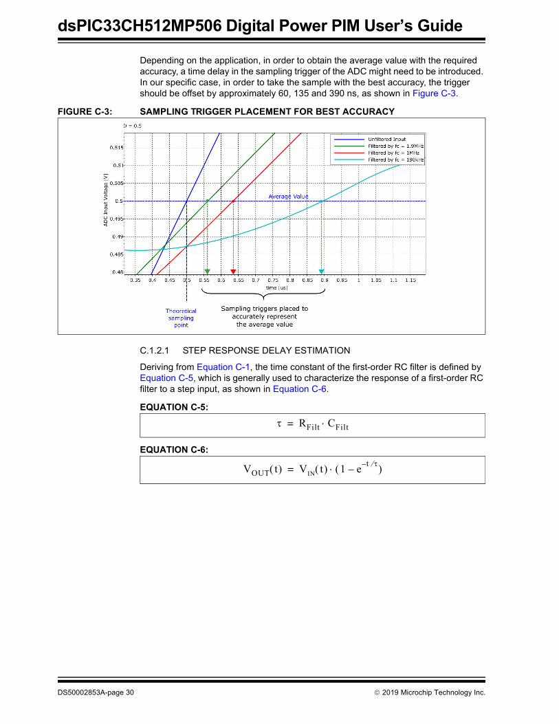
Depending on the application, in order to obtain the average value with the required accuracy, a time delay in the sampling trigger of the ADC might need to be introduced. In our specific case, in order to take the sample with the best accuracy, the trigger should be offset by approximately 60, 135 and 390 ns, as shown in Figure C-3.
FIGURE C-3: SAMPLING TRIGGER PLACEMENT FOR BEST ACCURACY
C.1.2.1 STEP RESPONSE DELAY ESTIMATION
Deriving from Equation C-1, the time constant of the first-order RC filter is defined by Equation C-5, which is generally used to characterize the response of a first-order RC filter to a step input, as shown in Equation C-6.
EQUATION C-5:
EQUATION C-6:
RFilt CFilt=
VOUT t VIN t 1 et–
– =
DS50002853A-page 30 2019 Microchip Technology Inc.
Characterization Data
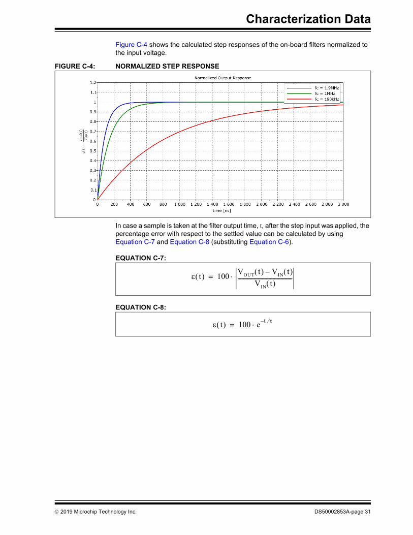
Figure C-4 shows the calculated step responses of the on-board filters normalized to the input voltage.
FIGURE C-4: NORMALIZED STEP RESPONSE
In case a sample is taken at the filter output time, t, after the step input was applied, the percentage error with respect to the settled value can be calculated by using Equation C-7 and Equation C-8 (substituting Equation C-6).
EQUATION C-7:
EQUATION C-8:
t 100VOUT t VIN t –
VIN t ----------------------------------------=
t 100 et– =
2019 Microchip Technology Inc. DS50002853A-page 31
dsPIC33CH512MP506 Digital Power PIM User’s Guide
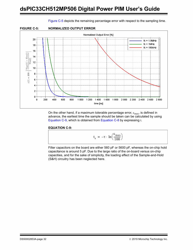
Figure C-5 depicts the remaining percentage error with respect to the sampling time.
FIGURE C-5: NORMALIZED OUTPUT ERROR
On the other hand, if a maximum tolerable percentage error, max, is defined in advance, the earliest time the sample should be taken can be calculated by using Equation C-9, which is obtained from Equation C-8 by expressing t.
EQUATION C-9:
Filter capacitors on the board are either 560 pF or 5600 pF, whereas the on-chip hold capacitance is around 5 pF. Due to the large ratio of the on-board versus on-chip capacities, and for the sake of simplicity, the loading effect of the Sample-and-Hold (S&H) circuitry has been neglected here.
ts –max100----------- ln=
DS50002853A-page 32 2019 Microchip Technology Inc.
Characterization Data
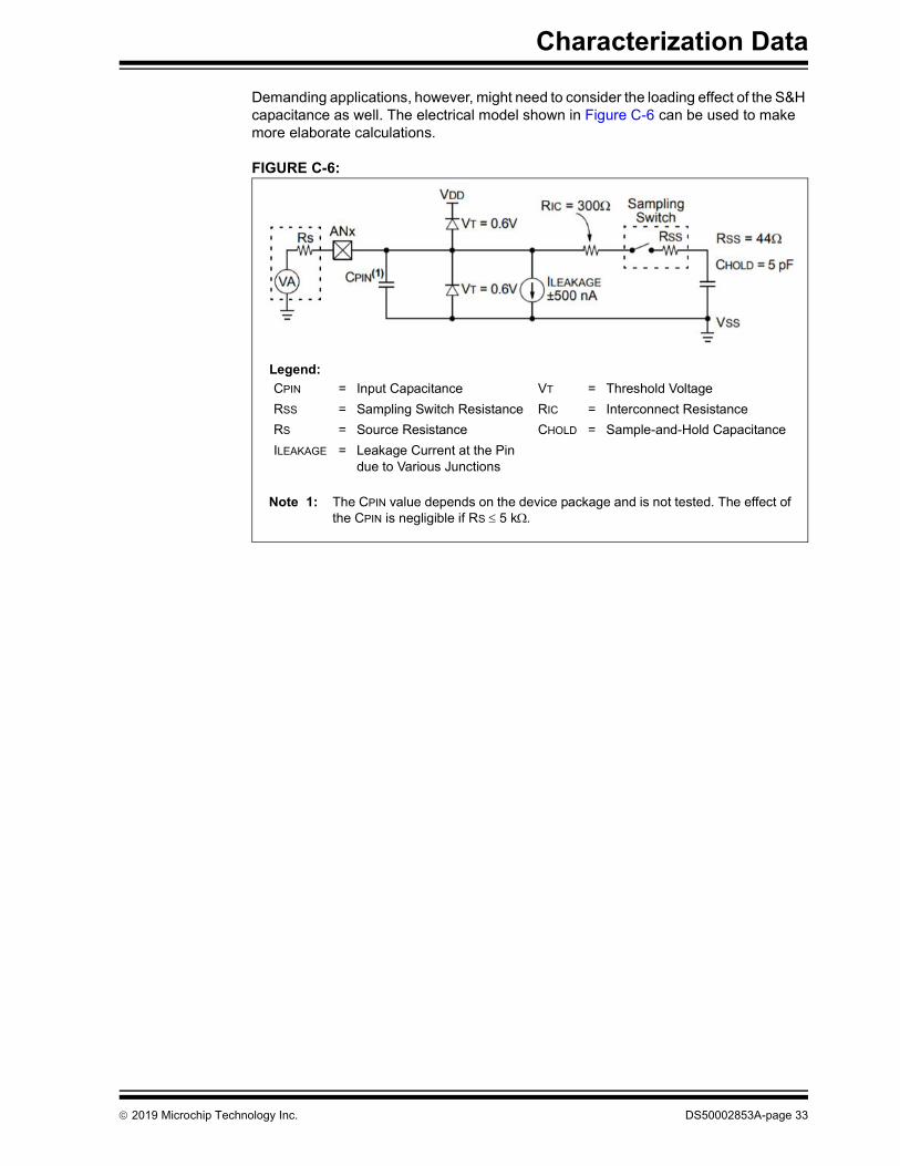
Demanding applications, however, might need to consider the loading effect of the S&H capacitance as well. The electrical model shown in Figure C-6 can be used to make more elaborate calculations.
FIGURE C-6:
Legend:
CPIN = Input Capacitance VT = Threshold Voltage
RSS = Sampling Switch Resistance RIC = Interconnect Resistance
RS = Source Resistance CHOLD = Sample-and-Hold Capacitance
ILEAKAGE = Leakage Current at the Pindue to Various Junctions
Note 1: The CPIN value depends on the device package and is not tested. The effect of the CPIN is negligible if RS 5 k.
2019 Microchip Technology Inc. DS50002853A-page 33

DS50002853A-page 34 2019 Microchip Technology Inc.
AMERICASCorporate Office2355 West Chandler Blvd.Chandler, AZ 85224-6199Tel: 480-792-7200 Fax: 480-792-7277Technical Support: http://www.microchip.com/supportWeb Address: www.microchip.com
AtlantaDuluth, GA Tel: 678-957-9614 Fax: 678-957-1455
Austin, TXTel: 512-257-3370
BostonWestborough, MA Tel: 774-760-0087 Fax: 774-760-0088
ChicagoItasca, IL Tel: 630-285-0071 Fax: 630-285-0075
DallasAddison, TX Tel: 972-818-7423 Fax: 972-818-2924
DetroitNovi, MI Tel: 248-848-4000
Houston, TX Tel: 281-894-5983
IndianapolisNoblesville, IN Tel: 317-773-8323Fax: 317-773-5453Tel: 317-536-2380
Los AngelesMission Viejo, CA Tel: 949-462-9523Fax: 949-462-9608Tel: 951-273-7800
Raleigh, NC Tel: 919-844-7510
New York, NY Tel: 631-435-6000
San Jose, CA Tel: 408-735-9110Tel: 408-436-4270
Canada - TorontoTel: 905-695-1980 Fax: 905-695-2078
ASIA/PACIFICAustralia - SydneyTel: 61-2-9868-6733
China - BeijingTel: 86-10-8569-7000
China - ChengduTel: 86-28-8665-5511
China - ChongqingTel: 86-23-8980-9588
China - DongguanTel: 86-769-8702-9880
China - GuangzhouTel: 86-20-8755-8029
China - HangzhouTel: 86-571-8792-8115
China - Hong Kong SARTel: 852-2943-5100
China - NanjingTel: 86-25-8473-2460
China - QingdaoTel: 86-532-8502-7355
China - ShanghaiTel: 86-21-3326-8000
China - ShenyangTel: 86-24-2334-2829
China - ShenzhenTel: 86-755-8864-2200
China - SuzhouTel: 86-186-6233-1526
China - WuhanTel: 86-27-5980-5300
China - XianTel: 86-29-8833-7252
China - XiamenTel: 86-592-2388138
China - ZhuhaiTel: 86-756-3210040
ASIA/PACIFICIndia - BangaloreTel: 91-80-3090-4444
India - New DelhiTel: 91-11-4160-8631
India - PuneTel: 91-20-4121-0141
Japan - OsakaTel: 81-6-6152-7160
Japan - TokyoTel: 81-3-6880- 3770
Korea - DaeguTel: 82-53-744-4301
Korea - SeoulTel: 82-2-554-7200
Malaysia - Kuala LumpurTel: 60-3-7651-7906
Malaysia - PenangTel: 60-4-227-8870
Philippines - ManilaTel: 63-2-634-9065
SingaporeTel: 65-6334-8870
Taiwan - Hsin ChuTel: 886-3-577-8366
Taiwan - KaohsiungTel: 886-7-213-7830
Taiwan - TaipeiTel: 886-2-2508-8600
Thailand - BangkokTel: 66-2-694-1351
Vietnam - Ho Chi MinhTel: 84-28-5448-2100
EUROPEAustria - WelsTel: 43-7242-2244-39Fax: 43-7242-2244-393
Denmark - CopenhagenTel: 45-4450-2828 Fax: 45-4485-2829
Finland - EspooTel: 358-9-4520-820
France - ParisTel: 33-1-69-53-63-20 Fax: 33-1-69-30-90-79
Germany - GarchingTel: 49-8931-9700
Germany - HaanTel: 49-2129-3766400
Germany - HeilbronnTel: 49-7131-67-3636
Germany - KarlsruheTel: 49-721-625370
Germany - MunichTel: 49-89-627-144-0 Fax: 49-89-627-144-44
Germany - RosenheimTel: 49-8031-354-560
Israel - Ra’anana Tel: 972-9-744-7705
Italy - Milan Tel: 39-0331-742611 Fax: 39-0331-466781
Italy - PadovaTel: 39-049-7625286
Netherlands - DrunenTel: 31-416-690399 Fax: 31-416-690340
Norway - TrondheimTel: 47-7288-4388
Poland - WarsawTel: 48-22-3325737
Romania - BucharestTel: 40-21-407-87-50
Spain - MadridTel: 34-91-708-08-90Fax: 34-91-708-08-91
Sweden - GothenbergTel: 46-31-704-60-40
Sweden - StockholmTel: 46-8-5090-4654
UK - WokinghamTel: 44-118-921-5800Fax: 44-118-921-5820
Worldwide Sales and Service
08/15/18


![AppNote - PIM - Mitigating Ext. Sources of PIM [11410-00756A]](https://img.pdfslide.us/doc/110x75/55cf9b4e550346d033a5882d/appnote-pim-mitigating-ext-sources-of-pim-11410-00756a.jpg)