Embed Size (px)
Citation preview
© 2007 Microchip Technology Inc. DS70138E
dsPIC30F3014/4013Data Sheet
High-Performance, 16-Bit
Digital Signal Controllers
DS70138E-page ii © 2007 Microchip Technology Inc.
Information contained in this publication regarding deviceapplications and the like is provided only for your convenienceand may be superseded by updates. It is your responsibility toensure that your application meets with your specifications.MICROCHIP MAKES NO REPRESENTATIONS ORWARRANTIES OF ANY KIND WHETHER EXPRESS ORIMPLIED, WRITTEN OR ORAL, STATUTORY OROTHERWISE, RELATED TO THE INFORMATION,INCLUDING BUT NOT LIMITED TO ITS CONDITION,QUALITY, PERFORMANCE, MERCHANTABILITY ORFITNESS FOR PURPOSE. Microchip disclaims all liabilityarising from this information and its use. Use of Microchipdevices in life support and/or safety applications is entirely atthe buyer’s risk, and the buyer agrees to defend, indemnify andhold harmless Microchip from any and all damages, claims,suits, or expenses resulting from such use. No licenses areconveyed, implicitly or otherwise, under any Microchipintellectual property rights.
Trademarks
The Microchip name and logo, the Microchip logo, Accuron, dsPIC, KEELOQ, microID, MPLAB, PIC, PICmicro, PICSTART, PRO MATE, PowerSmart, rfPIC and SmartShunt are registered trademarks of Microchip Technology Incorporated in the U.S.A. and other countries.
AmpLab, FilterLab, Migratable Memory, MXDEV, MXLAB, SEEVAL, SmartSensor and The Embedded Control Solutions Company are registered trademarks of Microchip Technology Incorporated in the U.S.A.
Analog-for-the-Digital Age, Application Maestro, CodeGuard, dsPICDEM, dsPICDEM.net, dsPICworks, ECAN, ECONOMONITOR, FanSense, FlexROM, fuzzyLAB, In-Circuit Serial Programming, ICSP, ICEPIC, Linear Active Thermistor, Mindi, MiWi, MPASM, MPLIB, MPLINK, PICkit, PICDEM, PICDEM.net, PICLAB, PICtail, PowerCal, PowerInfo, PowerMate, PowerTool, REAL ICE, rfLAB, rfPICDEM, Select Mode, Smart Serial, SmartTel, Total Endurance, UNI/O, WiperLock and ZENA are trademarks of Microchip Technology Incorporated in the U.S.A. and other countries.
SQTP is a service mark of Microchip Technology Incorporated in the U.S.A.
All other trademarks mentioned herein are property of their respective companies.
© 2007, Microchip Technology Incorporated, Printed in the U.S.A., All Rights Reserved.
Printed on recycled paper.
Note the following details of the code protection feature on Microchip devices:
• Microchip products meet the specification contained in their particular Microchip Data Sheet.
• Microchip believes that its family of products is one of the most secure families of its kind on the market today, when used in the intended manner and under normal conditions.
• There are dishonest and possibly illegal methods used to breach the code protection feature. All of these methods, to our knowledge, require using the Microchip products in a manner outside the operating specifications contained in Microchip’s Data Sheets. Most likely, the person doing so is engaged in theft of intellectual property.
• Microchip is willing to work with the customer who is concerned about the integrity of their code.
• Neither Microchip nor any other semiconductor manufacturer can guarantee the security of their code. Code protection does not mean that we are guaranteeing the product as “unbreakable.”
Code protection is constantly evolving. We at Microchip are committed to continuously improving the code protection features of ourproducts. Attempts to break Microchip’s code protection feature may be a violation of the Digital Millennium Copyright Act. If such actsallow unauthorized access to your software or other copyrighted work, you may have a right to sue for relief under that Act.
Microchip received ISO/TS-16949:2002 certification for its worldwide headquarters, design and wafer fabrication facilities in Chandler and Tempe, Arizona, Gresham, Oregon and Mountain View, California. The Company’s quality system processes and procedures are for its PIC®
MCUs and dsPIC DSCs, KEELOQ® code hopping devices, Serial EEPROMs, microperipherals, nonvolatile memory and analog products. In addition, Microchip’s quality system for the design and manufacture of development systems is ISO 9001:2000 certified.

© 2007 Microchip Technology Inc. DS70138E-page 1
dsPIC30F3014/4013
High-Performance Modified RISC CPU:
• Modified Harvard architecture• C compiler optimized instruction set architecture
• Flexible addressing modes• 83 base instructions• 24-bit wide instructions, 16-bit wide data path
• Up to 48 Kbytes on-chip Flash program space• 2 Kbytes of on-chip data RAM• 1 Kbyte of nonvolatile data EEPROM
• 16 x 16-bit working register array• Up to 30 MIPS operation:
- DC to 40 MHz external clock input- 4 MHz-10 MHz oscillator input with
PLL active (4x, 8x, 16x)• Up to 33 interrupt sources:
- 8 user selectable priority levels
- 3 external interrupt sources- 4 processor traps
DSP Features:
• Dual data fetch• Modulo and Bit-Reversed modes
• Two 40-bit wide accumulators with optional saturation logic
• 17-bit x 17-bit single-cycle hardware fractional/integer multiplier
• All DSP instructions are single cycle- Multiply-Accumulate (MAC) operation
• Single-cycle ±16 shift
Peripheral Features:
• High-current sink/source I/O pins: 25 mA/25 mA• Up to five 16-bit timers/counters; optionally pair
up16-bit timers into 32-bit timer modules
• Up to four 16-bit Capture input functions• Up to four 16-bit Compare/PWM output functions• Data Converter Interface (DCI) supports common
audio Codec protocols, including I2S and AC’97• 3-wire SPI module (supports 4 Frame modes)• I2C™ module supports Multi-Master/Slave mode
and 7-bit/10-bit addressing• Up to two addressable UART modules with FIFO
buffers• CAN bus module compliant with CAN 2.0B
standard
Analog Features:
• 12-bit Analog-to-Digital Converter (ADC) with:
- 200 ksps conversion rate- Up to 13 input channels- Conversion available during Sleep and Idle
• Programmable Low-Voltage Detection (PLVD)• Programmable Brown-out Reset
Special Microcontroller Features:
• Enhanced Flash program memory:- 10,000 erase/write cycle (min.) for
industrial temperature range, 100K (typical)• Data EEPROM memory:
- 100,000 erase/write cycle (min.) for industrial temperature range, 1M (typical)
• Self-reprogrammable under software control• Power-on Reset (POR), Power-up Timer (PWRT)
and Oscillator Start-up Timer (OST)• Flexible Watchdog Timer (WDT) with on-chip
low-power RC oscillator for reliable operation• Fail-Safe Clock Monitor operation:
- Detects clock failure and switches to on-chip low-power RC oscillator
Note: This data sheet summarizes features of this groupof dsPIC30F devices and is not intended to be a completereference source. For more information on the CPU,peripherals, register descriptions and general devicefunctionality, refer to the “dsPIC30F Family ReferenceManual” (DS70046). For more information on the deviceinstruction set and programming, refer to the “dsPIC30F/33F Programmer’s Reference Manual” (DS70157).
dsPIC30F3014/4013 High-Performance, 16-Bit Digital Signal Controllers
dsPIC30F3014/4013
DS70138E-page 2 © 2007 Microchip Technology Inc.
Special Microcontroller Features (Cont.):
• Programmable code protection• In-Circuit Serial Programming™ (ICSP™)
• Selectable Power Management modes: - Sleep, Idle and Alternate Clock modes
CMOS Technology:
• Low-power, high-speed Flash technology
• Wide operating voltage range (2.5V to 5.5V)• Industrial and Extended temperature ranges• Low-power consumption
dsPIC30F3014/4013 Controller Family
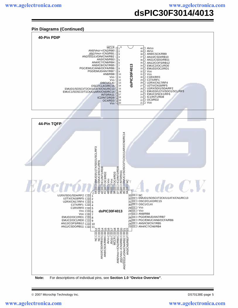
Pin Diagrams
Device PinsProgram Memory
SRAM Bytes
EEPROMBytes
Timer 16-bit
InputCap
Output Comp/
Std PWM
Codec Interface
A/D 12-bit 200 Ksps U
AR
T
SP
I
I2 C™
CA
N
Bytes Instructions
dsPIC30F3014 40/44 24K 8K 2048 1024 3 2 2 - 13 ch 2 1 1 0
dsPIC30F4013 40/44 48K 16K 2048 1024 5 4 4 AC’97, I2S 13 ch 2 1 1 1
PGD/EMUD/AN7/RB7PGC/EMUC/AN6/OCFA/RB6
RF0RF1
RD2IC1/INT1/RD8
AN8/RB8
1234567891011121314151617181920
4039383736353433323130292827262524232221
dsP
IC30
F30
14
MCLR
VDDVss
IC2/INT2/RD9
EMUC1/SOSCO/T1CK/U1ARX/CN0/RC14EMUD1/SOSCI/T2CK/U1ATX/CN1/RC13
OSC2/CLKO/RC15OSC1/CLKI
AN9/RB9AN10/RB10AN11/RB11AN12/RB12
EMUD2/OC2/RD1
AVDDAVss
RD3
VssVDD
EMUC3/SCK1/RF6
U1RX/SDI1/SDA/RF2EMUD3/U1TX/SDO1/SCL/RF3
EMUC2/OC1/RD0
VDD
U2RX/CN17/RF4U2TX/CN18/RF5
AN4/CN6/RB4
AN2/SS1/LVDIN/CN4/RB2AN1/VREF-/CN3/RB1AN0/VREF+/CN2/RB0
AN5/CN7/RB5
INT0/RA11
Vss
AN3/CN5/RB3
40-Pin PDIP
© 2007 Microchip Technology Inc. DS70138E-page 3
dsPIC30F3014/4013
Pin Diagrams (Continued)
Note: For descriptions of individual pins, see Section 1.0 “Device Overview”.
1011
23456
1
18 19 20 21 2212 13 14 15
38
87
44 43 42 41 40 3916 17
2930313233
232425262728
36 3435
9
37
EM
UD
3/U
1TX
/SD
O1/
SC
L/R
F3
EM
UC
3/S
CK
1/R
F6
IC1/
NT
1/R
D8
RD
2V
DD
EM
UC
1/S
OS
CO
/T1C
K/U
1AR
X/C
N0/
RC
14N
C
VS
S
RD
3IC
2/IN
T2/
RD
9IN
T0/
RA
11
AN
3/C
N5/
RB
3A
N2/
SS
1/LV
DIN
/CN
4/R
B2
AN
1/V
RE
F-/
CN
3/R
B1
AN
0/V
RE
F+
/CN
2/R
B0
MC
LRNC
AV
DD
AV
SS
AN
9/R
B9
AN
10/R
B10
AN12/RB12EMUC2/OC1/RD0EMUD2/OC2/RD1
VDD
VSSRF0RF1
U2RX/CN17/RF4U2TX/CN18/RF5
U1RX/SDI1/SDA/RF2
AN4/CN6/RB4AN5/CN7/RB5PGC/EMUC/AN6/OCFA/RB6PGD/EMUD/AN7/RB7AN8/RB8
NC
VDD
VSS
OSC1/CLKIOSC2/CLKO/RC15EMUD1/SOSCI/T2CK/U1ATX/CN1/RC13
dsPIC30F3014
44-Pin TQFP
AN11/RB11
NC
dsPIC30F3014/4013
DS70138E-page 4 © 2007 Microchip Technology Inc.
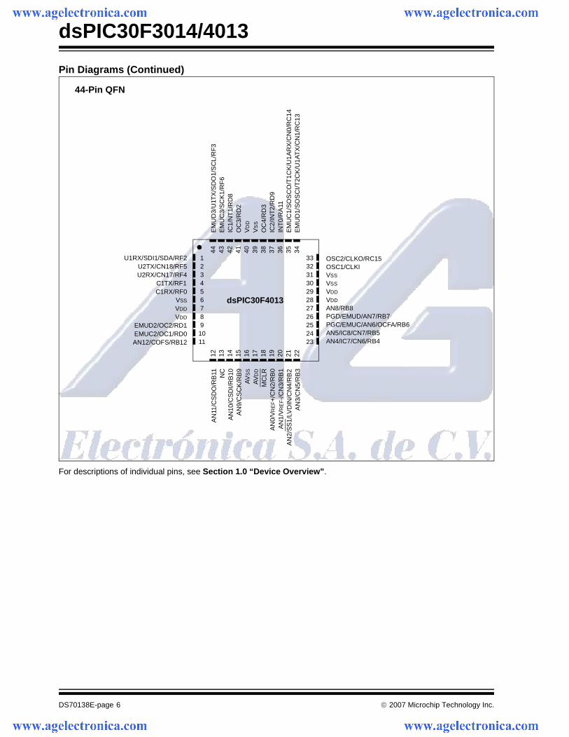
Pin Diagrams (Continued)
Note: For descriptions of individual pins, see Section 1.0 “Device Overview”.
44-Pin QFN
dsPIC30F3014
EM
UD
3/U
1TX
/SD
O1/
SC
L/R
F3
EM
UC
3/S
CK
1/R
F6
IC1/
INT
1/R
D8
RD
2V
DD
EM
UC
1/S
OS
CO
/T1C
K/U
1AR
X/C
N0/
RC
14E
MU
D1/
SO
SC
I/T2C
K/U
1AT
X/C
N1/
RC
13
VS
S
RD
3IC
2/IN
T2/
RD
9IN
T0/
RA
11
AN4/CN6/RB4AN5/CN7/RB5PGC/EMUC/AN6/OCFA/RB6PGD/EMUD/AN7/RB7AN8/RB8
OSC2/CLKO/RC15
VDD
VDD
VSS
VSS
OSC1/CLKI
EMUC2/OC1/RD0EMUD2/OC2/RD1
VDD
VDD
VSS
RF0RF1
U2RX/CN17/RF4U2TX/CN18/RF5
U1RX/SDI1/SDA/RF2
AN12/RB12
AN
3/C
N5/
RB
3A
N2/
SS
1/LV
DIN
/CN
4/R
B2
AN
1/V
RE
F-/
CN
3/R
B1
AN
0/V
RE
F+
/CN
2/R
B0
MC
LR
AN
11/R
B11
AV
DD
AV
SS
AN
9/R
B9
AN
10/R
B10NC
44 43 42 41 40 39 38 37 36 35
12 13 14 15 16 17 18 19 20 213
3029282726252423
45
7891011
12 32
31
622
33
34
© 2007 Microchip Technology Inc. DS70138E-page 5
dsPIC30F3014/4013
Pin Diagrams (Continued)
Note: For descriptions of individual pins, see Section 1.0 “Device Overview”.
PGD/EMUD/AN7/RB7PGC/EMUC/AN6/OCFA/RB6
C1RX/RF0C1TX/RF1
OC3/RD2IC1/INT1/RD8
AN8/RB8
1234567891011121314151617181920
4039383736353433323130292827262524232221
dsP
IC30
F40
13
MCLR
VDDVSS
IC2/INT2/RD9
EMUC1/SOSCO/T1CK/U1ARX/CN0/RC14EMUD1/SOSCI/T2CK/U1ATX/CN1/RC13
OSC2/CLKO/RC15OSC1/CLKI
AN9/CSCK/RB9AN10/CSDI/RB10AN11/CSDO/RB11AN12/COFS/RB12
EMUD2/OC2/RD1
AVDDAVSS
OC4/RD3
VSSVDD
EMUC3/SCK1/RF6
U1RX/SDI1/SDA/RF2EMUD3/U1TX/SDO1/SCL/RF3
EMUC2/OC1/RD0
VDD
U2RX/CN17/RF4U2TX/CN18/RF5
AN4/IC7/CN6/RB4
AN2/SS1/LVDIN/CN4/RB2AN1/VREF-/CN3/RB1AN0/VREF+/CN2/RB0
AN5/IC8/CN7/RB5
INT0/RA11
VSS
AN3/CN5/RB3
40-Pin PDIP
1011
23456
1
18 19 20 21 2212 13 14 15
38
87
44 43 42 41 40 3916 17
2930313233
232425262728
36 3435
9
37
EM
UD
3/U
1TX
/SD
O1/
SC
L/R
F3
EM
UC
3/S
CK
1/R
F6
IC1/
INT
1/R
D8
OC
3/R
D2
VD
D
EM
UC
1/S
OS
CO
/T1C
K/U
1AR
X/C
N0/
RC
14N
C
VS
S
OC
4/R
D3
IC2/
INT
2/R
D9
INT
0/R
A11
AN
3/C
N5/
RB
3A
N2/
SS
1 /LV
DIN
/CN
4/R
B2
AN
1/V
RE
F-/
CN
3/R
B1
AN
0/V
RE
F+
/CN
2/R
B0
MC
LRNC
AV
DD
AV
SS
AN
9/C
SC
K/R
B9
AN
10/C
SD
I/RB
10
AN12/COFS/RB12EMUC2/OC1/RD0EMUD2/OC2/RD1
VDD
VSSC1RX/RF0C1TX/RF1
U2RX/CN17/RF4U2TX/CN18/RF5
U1RX/SDI1/SDA/RF2
AN4/IC7/CN6/RB4AN5/IC8/CN7/RB5PGC/EMUC/AN6/OCFA/RB6PGD/EMUD/AN7/RB7AN8/RB8
NC
VDD
VSS
OSC1/CLKIOSC2/CLKO/RC15EMUD1/SOSCI/T2CK/U1ATX/CN1/RC13
dsPIC30F4013
44-Pin TQFP
AN11/CSDO/RB11
NC
dsPIC30F3014/4013
DS70138E-page 6 © 2007 Microchip Technology Inc.
Pin Diagrams (Continued)
For descriptions of individual pins, see Section 1.0 “Device Overview”.
44-Pin QFN
44 43 42 41 40 39 38 37 36 35
12 13 14 15 16 17 18 19 20 21
33029282726252423
45
7891011
12 32
31
dsPIC30F4013622
33
34
EM
UD
3/U
1TX
/SD
O1/
SC
L/R
F3
EM
UC
3/S
CK
1/R
F6
IC1/
NT
1/R
D8
OC
3/R
D2
VD
D
EM
UC
1/S
OS
CO
/T1C
K/U
1AR
X/C
N0/
RC
14E
MU
D1/
SO
SC
I/T2C
K/U
1AT
X/C
N1/
RC
13
VS
S
OC
4/R
D3
IC2/
INT
2/R
D9
INT
0/R
A11
AN4/IC7/CN6/RB4AN5/IC8/CN7/RB5PGC/EMUC/AN6/OCFA/RB6PGD/EMUD/AN7/RB7AN8/RB8
OSC2/CLKO/RC15
VDD
VDD
VSS
VSS
OSC1/CLKI
EMUC2/OC1/RD0EMUD2/OC2/RD1
VDD
VDD
VSS
C1RX/RF0C1TX/RF1
U2RX/CN17/RF4U2TX/CN18/RF5
U1RX/SDI1/SDA/RF2
AN12/COFS/RB12
AN
3/C
N5/
RB
3A
N2/
SS
1/LV
DIN
/CN
4/R
B2
AN
1/V
RE
F-/
CN
3/R
B1
AN
0/V
RE
F+
/CN
2/R
B0
MC
LR
AN
11/C
SD
O/R
B11
AV
DD
AV
SS
AN
9/C
SC
K/R
B9
AN
10/C
SD
I/RB
10NC
© 2007 Microchip Technology Inc. DS70138E-page 7
dsPIC30F3014/4013
Table of Contents
1.0 Device Overview ......................................................................................................................................................................... 92.0 CPU Architecture Overview ....................................................................................................................................................... 133.0 Memory Organization ................................................................................................................................................................ 234.0 Address Generator Units ........................................................................................................................................................... 355.0 Flash Program Memory ............................................................................................................................................................. 416.0 Data EEPROM Memory ............................................................................................................................................................ 477.0 I/O Ports .................................................................................................................................................................................... 518.0 Interrupts ................................................................................................................................................................................... 559.0 Timer1 Module .......................................................................................................................................................................... 6310.0 Timer2/3 Module ....................................................................................................................................................................... 6711.0 Timer4/5 Module ...................................................................................................................................................................... 7312.0 Input Capture Module ................................................................................................................................................................ 7713.0 Output Compare Module ........................................................................................................................................................... 8114.0 I2C™ Module ............................................................................................................................................................................ 8515.0 SPI Module ................................................................................................................................................................................ 9316.0 Universal Asynchronous Receiver Transmitter (UART) Module ............................................................................................... 9717.0 CAN Module ............................................................................................................................................................................ 10518.0 Data Converter Interface (DCI) Module ................................................................................................................................... 11519.0 12-bit Analog-to-Digital Converter (ADC) Module ................................................................................................................... 12520.0 System Integration .................................................................................................................................................................. 13521.0 Instruction Set Summary ......................................................................................................................................................... 15322.0 Development Support .............................................................................................................................................................. 16123.0 Electrical Characteristics ......................................................................................................................................................... 16524.0 Packaging Information ............................................................................................................................................................. 203Index ................................................................................................................................................................................................. 209The Microchip Web Site .................................................................................................................................................................... 215Customer Change Notification Service ............................................................................................................................................. 215Customer Support ............................................................................................................................................................................. 215Reader Response ............................................................................................................................................................................. 216Product Identification System ........................................................................................................................................................... 217
TO OUR VALUED CUSTOMERS
It is our intention to provide our valued customers with the best documentation possible to ensure successful use of your Microchipproducts. To this end, we will continue to improve our publications to better suit your needs. Our publications will be refined andenhanced as new volumes and updates are introduced.
If you have any questions or comments regarding this publication, please contact the Marketing Communications Department viaE-mail at [email protected] or fax the Reader Response Form in the back of this data sheet to (480) 792-4150. Wewelcome your feedback.
Most Current Data SheetTo obtain the most up-to-date version of this data sheet, please register at our Worldwide Web site at:
http://www.microchip.com
You can determine the version of a data sheet by examining its literature number found on the bottom outside corner of any page.The last character of the literature number is the version number, (e.g., DS30000A is version A of document DS30000).
ErrataAn errata sheet, describing minor operational differences from the data sheet and recommended workarounds, may exist for currentdevices. As device/documentation issues become known to us, we will publish an errata sheet. The errata will specify the revisionof silicon and revision of document to which it applies.
To determine if an errata sheet exists for a particular device, please check with one of the following:
• Microchip’s Worldwide Web site; http://www.microchip.com• Your local Microchip sales office (see last page)When contacting a sales office, please specify which device, revision of silicon and data sheet (include literature number) you areusing.
Customer Notification SystemRegister on our web site at www.microchip.com to receive the most current information on all of our products.

dsPIC30F3014/4013
DS70138E-page 8 © 2007 Microchip Technology Inc.
NOTES:
© 2007 Microchip Technology Inc. DS70138E-page 9
dsPIC30F3014/4013
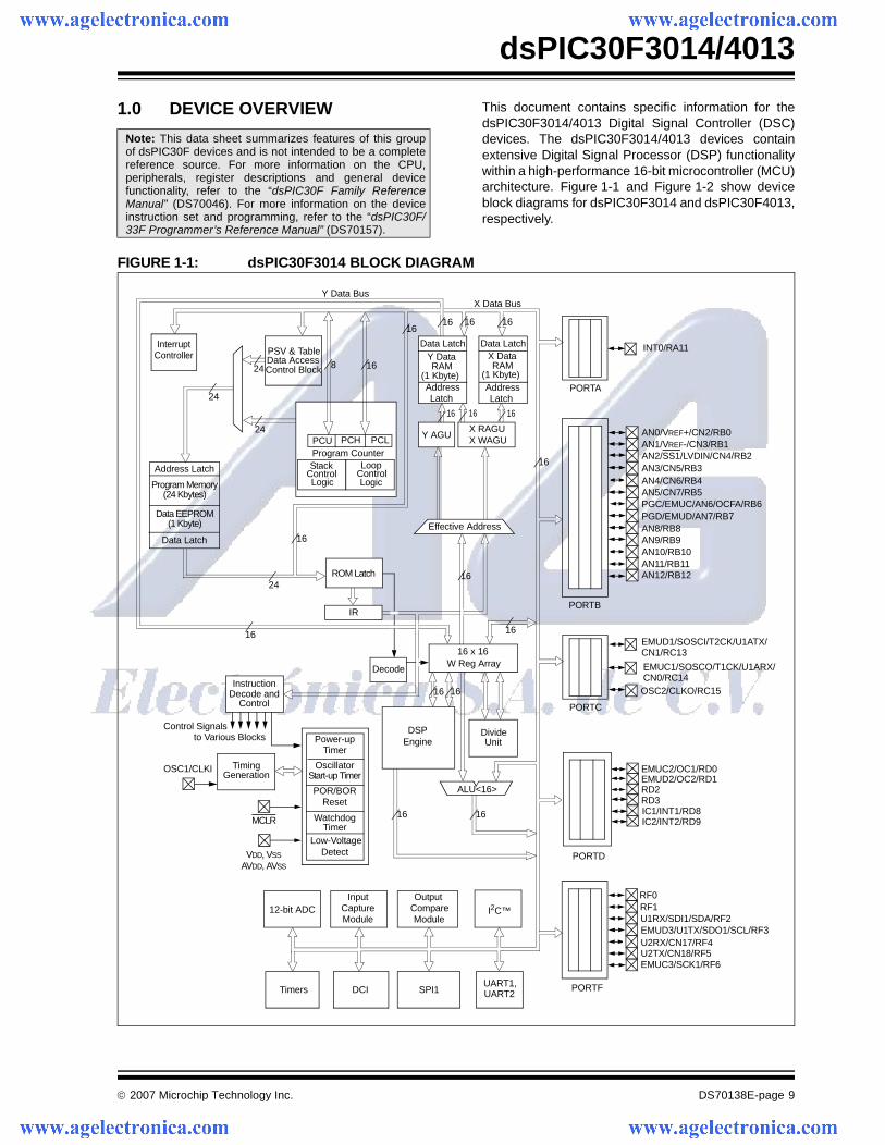
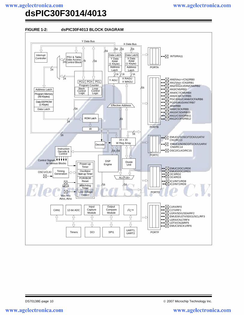
1.0 DEVICE OVERVIEW This document contains specific information for thedsPIC30F3014/4013 Digital Signal Controller (DSC)devices. The dsPIC30F3014/4013 devices containextensive Digital Signal Processor (DSP) functionalitywithin a high-performance 16-bit microcontroller (MCU)architecture. Figure 1-1 and Figure 1-2 show deviceblock diagrams for dsPIC30F3014 and dsPIC30F4013,respectively.
FIGURE 1-1: dsPIC30F3014 BLOCK DIAGRAM
Note: This data sheet summarizes features of this groupof dsPIC30F devices and is not intended to be a completereference source. For more information on the CPU,peripherals, register descriptions and general devicefunctionality, refer to the “dsPIC30F Family ReferenceManual” (DS70046). For more information on the deviceinstruction set and programming, refer to the “dsPIC30F/33F Programmer’s Reference Manual” (DS70157).
AN8/RB8AN9/RB9AN10/RB10AN11/RB11
Power-upTimer
OscillatorStart-up Timer
POR/BORReset
WatchdogTimer
InstructionDecode and
Control
OSC1/CLKI
MCLR
VDD, VSS
AN4/CN6/RB4
AN12/RB12
Low-VoltageDetect
UART1,
TimingGeneration
AN5/CN7/RB5
16
PCH PCLProgram Counter
ALU<16>
16
24
24
24
24
X Data Bus
IR
I2C™
DCI
PGC/EMUC/AN6/OCFA/RB6PGD/EMUD/AN7/RB7
PCU
12-bit ADC
Timers
U2TX/CN18/RF5EMUC3/SCK1/RF6
InputCaptureModule
OutputCompareModule
EMUD1/SOSCI/T2CK/U1ATX/
PORTB
RF0RF1U1RX/SDI1/SDA/RF2EMUD3/U1TX/SDO1/SCL/RF3
PORTD
16
16 16
16 x 16W Reg Array
Divide UnitEngine
DSP
Decode
ROM Latch
16
Y Data Bus
Effective Address
X RAGUX WAGU Y AGU AN0/VREF+/CN2/RB0
AN1/VREF-/CN3/RB1AN2/SS1/LVDIN/CN4/RB2AN3/CN5/RB3
OSC2/CLKO/RC15
U2RX/CN17/RF4
AVDD, AVSS
UART2
16
16
16
16
16
PORTC
PORTF
16
16
16
16
8
InterruptController PSV & Table
Data AccessControl Block
StackControl Logic
LoopControlLogic
Data LatchData LatchY Data
(1 Kbyte)RAM
X Data
(1 Kbyte)RAM
AddressLatch
AddressLatch
Control Signals to Various Blocks
EMUC2/OC1/RD0EMUD2/OC2/RD1RD2RD3IC1/INT1/RD8IC2/INT2/RD9
16
SPI1
Address Latch
Program Memory(24 Kbytes)
Data Latch
Data EEPROM(1 Kbyte)
16
CN1/RC13
EMUC1/SOSCO/T1CK/U1ARX/CN0/RC14
PORTA
INT0/RA11
dsPIC30F3014/4013
DS70138E-page 10 © 2007 Microchip Technology Inc.
FIGURE 1-2: dsPIC30F4013 BLOCK DIAGRAM
AN8/RB8AN9/CSCK/RB9AN10/CSDI/RB10AN11/CSDO/RB11
Power-upTimer
OscillatorStart-up Timer
POR/BORReset
WatchdogTimer
InstructionDecode &Control
OSC1/CLKI
MCLR
VDD, VSS
AN4/IC7/CN6/RB4
AN12/COFS/RB12
Low-VoltageDetect
TimingGeneration
AN5/IC8/CN7/RB5
16
PCH PCLProgram Counter
ALU<16>
16
24
24
24
24
X Data Bus
IR
PGC/EMUC/AN6/OCFA/RB6PGD/EMUD/AN7/RB7
PCU
U2TX/CN18/RF5EMUC3/SCK1/RF6
EMUD1/SOSCI/T2CK/U1ATX/
PORTB
C1RX/RF0C1TX/RF1U1RX/SDI1/SDA/RF2EMUD3/U1TX/SDO1/SCL/RF3
PORTD
16
16 16
16 x 16W Reg Array
Divide Unit Engine
DSP
Decode
ROM Latch
16
Y Data Bus
Effective Address
X RAGUX WAGU Y AGU AN0/VREF+/CN2/RB0
AN1/VREF-/CN3/RB1AN2/SS1/LVDIN/CN4/RB2AN3/CN5/RB3
OSC2/CLKO/RC15
U2RX/CN17/RF4
AVDD, AVSS
16
16
16
16
16
PORTC
PORTF
16
16
16
16
8
InterruptController PSV & Table
Data AccessControl Block
StackControl Logic
LoopControlLogic
Data LatchData LatchY Data
(1 Kbyte)RAM
X Data
(1 Kbyte)RAM
AddressLatch
AddressLatch
Control Signals to Various Blocks
EMUC2/OC1/RD0EMUD2/OC2/RD1OC3/RD2OC4/RD3
IC1/INT1/RD8IC2/INT2/RD9
16
Address Latch
Program Memory(48 Kbytes)
Data Latch
Data EEPROM(1 Kbyte)
16
CN1/RC13
EMUC1/SOSCO/T1CK/U1ARX/CN0/RC14
PORTA
INT0/RA11
UART1,
I2C™
DCI
12-bit ADC
Timers
InputCaptureModule
OutputCompareModule
UART2SPI1
CAN1
© 2007 Microchip Technology Inc. DS70138E-page 11
dsPIC30F3014/4013
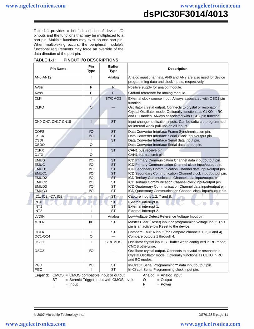
Table 1-1 provides a brief description of device I/Opinouts and the functions that may be multiplexed to aport pin. Multiple functions may exist on one port pin.When multiplexing occurs, the peripheral module’sfunctional requirements may force an override of thedata direction of the port pin.
TABLE 1-1: PINOUT I/O DESCRIPTIONS
Pin NamePin
TypeBufferType
Description
AN0-AN12 I Analog Analog input channels. AN6 and AN7 are also used for device programming data and clock inputs, respectively.
AVDD P P Positive supply for analog module.
AVSS P P Ground reference for analog module.
CLKI
CLKO
I
O
ST/CMOS
—
External clock source input. Always associated with OSC1 pin function.Oscillator crystal output. Connects to crystal or resonator in Crystal Oscillator mode. Optionally functions as CLKO in RC and EC modes. Always associated with OSC2 pin function.
CN0-CN7, CN17-CN18 I ST Input change notification inputs. Can be software programmed for internal weak pull-ups on all inputs.
COFSCSCKCSDICSDO
I/OI/OIO
STSTST—
Data Converter Interface Frame Synchronization pin.Data Converter Interface Serial Clock input/output pin.Data Converter Interface Serial data input pin.Data Converter Interface Serial data output pin.
C1RXC1TX
IO
ST—
CAN1 bus receive pin.CAN1 bus transmit pin.
EMUDEMUCEMUD1EMUC1EMUD2EMUC2EMUD3EMUC3
I/OI/OI/OI/OI/OI/OI/OI/O
STSTSTSTSTSTSTST
ICD Primary Communication Channel data input/output pin.ICD Primary Communication Channel clock input/output pin.ICD Secondary Communication Channel data input/output pin.ICD Secondary Communication Channel clock input/output pin.ICD Tertiary Communication Channel data input/output pin.ICD Tertiary Communication Channel clock input/output pin.ICD Quaternary Communication Channel data input/output pin.ICD Quaternary Communication Channel clock input/output pin.
IC1, IC2, IC7, IC8 I ST Capture inputs 1,2, 7 and 8.
INT0INT1INT2
III
STSTST
External interrupt 0.External interrupt 1.External interrupt 2.
LVDIN I Analog Low-Voltage Detect Reference Voltage Input pin.
MCLR I/P ST Master Clear (Reset) input or programming voltage input. This pin is an active-low Reset to the device.
OCFAOC1-OC4
IO
ST—
Compare Fault A input (for Compare channels 1, 2, 3 and 4).Compare outputs 1 through 4.
OSC1
OSC2
I
I/O
ST/CMOS
—
Oscillator crystal input. ST buffer when configured in RC mode; CMOS otherwise.Oscillator crystal output. Connects to crystal or resonator in Crystal Oscillator mode. Optionally functions as CLKO in RC and EC modes.
PGDPGC
I/OI
STST
In-Circuit Serial Programming™ data input/output pin.In-Circuit Serial Programming clock input pin.
Legend: CMOS = CMOS compatible input or output Analog = Analog input ST = Schmitt Trigger input with CMOS levels O = Output I = Input P = Power
dsPIC30F3014/4013
DS70138E-page 12 © 2007 Microchip Technology Inc.
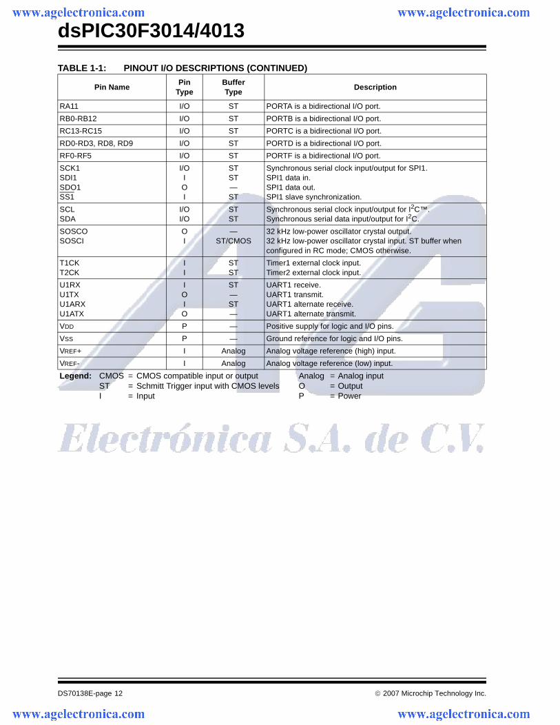
RA11 I/O ST PORTA is a bidirectional I/O port.
RB0-RB12 I/O ST PORTB is a bidirectional I/O port.
RC13-RC15 I/O ST PORTC is a bidirectional I/O port.
RD0-RD3, RD8, RD9 I/O ST PORTD is a bidirectional I/O port.
RF0-RF5 I/O ST PORTF is a bidirectional I/O port.
SCK1SDI1SDO1SS1
I/OIOI
STST—ST
Synchronous serial clock input/output for SPI1.SPI1 data in.SPI1 data out.SPI1 slave synchronization.
SCLSDA
I/OI/O
STST
Synchronous serial clock input/output for I2C™.Synchronous serial data input/output for I2C.
SOSCOSOSCI
OI
—ST/CMOS
32 kHz low-power oscillator crystal output. 32 kHz low-power oscillator crystal input. ST buffer when configured in RC mode; CMOS otherwise.
T1CKT2CK
II
STST
Timer1 external clock input.Timer2 external clock input.
U1RXU1TXU1ARXU1ATX
IOIO
ST—ST—
UART1 receive.UART1 transmit.UART1 alternate receive.UART1 alternate transmit.
VDD P — Positive supply for logic and I/O pins.
VSS P — Ground reference for logic and I/O pins.
VREF+ I Analog Analog voltage reference (high) input.
VREF- I Analog Analog voltage reference (low) input.
TABLE 1-1: PINOUT I/O DESCRIPTIONS (CONTINUED)
Pin NamePin
TypeBufferType
Description
Legend: CMOS = CMOS compatible input or output Analog = Analog input ST = Schmitt Trigger input with CMOS levels O = Output I = Input P = Power
© 2007 Microchip Technology Inc. DS70138E-page 13
dsPIC30F3014/4013
2.0 CPU ARCHITECTURE OVERVIEW
2.1 Core Overview
This section contains a brief overview of the CPUarchitecture of the dsPIC30F.
The core has a 24-bit instruction word. The ProgramCounter (PC) is 23 bits wide with the Least Significantbit (LSb) always clear (refer to Section 3.1 “ProgramAddress Space”), and the Most Significant bit (MSb)is ignored during normal program execution, except forcertain specialized instructions. Thus, the PC canaddress up to 4M instruction words of user programspace. An instruction prefetch mechanism is used tohelp maintain throughput. Program loop constructs,free from loop count management overhead, aresupported using the DO and REPEAT instructions, bothof which are interruptible at any point.
The working register array consists of 16-bit x 16-bitregisters, each of which can act as data, address or off-set registers. One working register (W15) operates asa software Stack Pointer for interrupts and calls.
The data space is 64 Kbytes (32K words) and is splitinto two blocks, referred to as X and Y data memory.Each block has its own independent Address Genera-tion Unit (AGU). Most instructions operate solelythrough the X memory, AGU, which provides theappearance of a single, unified data space. TheMultiply-Accumulate (MAC) class of dual source DSPinstructions operate through both the X and Y AGUs,splitting the data address space into two parts (seeSection 3.2 “Data Address Space”). The X and Ydata space boundary is device-specific and cannot bealtered by the user. Each data word consists of 2 bytes,and most instructions can address data either as wordsor bytes.
There are two methods of accessing data stored inprogram memory:
• The upper 32 Kbytes of data space memory can be mapped into the lower half (user space) of pro-gram space at any 16K program word boundary, defined by the 8-bit Program Space Visibility Page (PSVPAG) register. This lets any instruction access program space as if it were data space, with a limitation that the access requires an addi-tional cycle. Moreover, only the lower 16 bits of each instruction word can be accessed using this method.
• Linear indirect access of 32K word pages within program space is also possible using any working register, via table read and write instructions. Table read and write instructions can be used to access all 24 bits of an instruction word.
Overhead-free circular buffers (Modulo Addressing)are supported in both X and Y address spaces. This isprimarily intended to remove the loop overhead forDSP algorithms.
The X AGU also supports Bit-Reversed Addressing ondestination Effective Addresses to greatly simplify inputor output data reordering for radix-2 FFT algorithms.Refer to Section 4.0 “Address Generator Units” fordetails on Modulo and Bit-Reversed Addressing.
The core supports Inherent (no operand), Relative,Literal, Memory Direct, Register Direct, RegisterIndirect, Register Offset and Literal Offset Addressingmodes. Instructions are associated with predefinedaddressing modes, depending upon their functionalrequirements.
For most instructions, the core is capable of executinga data (or program data) memory read, a working reg-ister (data) read, a data memory write and a program(instruction) memory read per instruction cycle. As aresult, 3-operand instructions are supported, allowingC = A+B operations to be executed in a single cycle.
A DSP engine has been included to significantlyenhance the core arithmetic capability and throughput.It features a high-speed, 17-bit x 17-bit multiplier, a 40-bit ALU, two 40-bit saturating accumulators and a 40-bit bidirectional barrel shifter. Data in the accumulator,or any working register, can be shifted up to 15 bitsright, or 16 bits left in a single cycle. The DSP instruc-tions operate seamlessly with all other instructions andhave been designed for optimal real-time performance.The MAC class of instructions can concurrently fetchtwo data operands from memory while multiplying twoW registers. To enable this concurrent fetching of dataoperands, the data space has been split for theseinstructions and linear is for all others. This has beenachieved in a transparent and flexible manner bydedicating certain working registers to each addressspace for the MAC class of instructions.
Note: This data sheet summarizes features of this groupof dsPIC30F devices and is not intended to be a completereference source. For more information on the CPU,peripherals, register descriptions and general devicefunctionality, refer to the “dsPIC30F Family ReferenceManual” (DS70046). For more information on the deviceinstruction set and programming, refer to the “dsPIC30F/33F Programmer’s Reference Manual” (DS70157).
dsPIC30F3014/4013
DS70138E-page 14 © 2007 Microchip Technology Inc.
The core does not support a multi-stage instructionpipeline. However, a single-stage instruction prefetchmechanism is used, which accesses and partiallydecodes instructions a cycle ahead of execution, inorder to maximize available execution time. Mostinstructions execute in a single cycle with certainexceptions.
The core features a vectored exception processingstructure for traps and interrupts, with 62 independentvectors. The exceptions consist of up to 8 traps (ofwhich 4 are reserved) and 54 interrupts. Each interruptis prioritized based on a user-assigned priority between1 and 7 (1 being the lowest priority and 7 being thehighest), in conjunction with a predetermined ‘naturalorder’. Traps have fixed priorities ranging from 8 to 15.
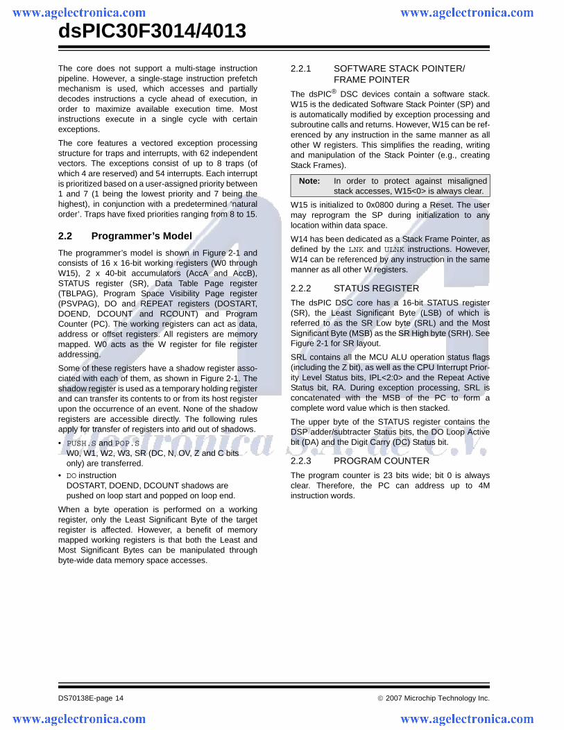
2.2 Programmer’s Model
The programmer’s model is shown in Figure 2-1 andconsists of 16 x 16-bit working registers (W0 throughW15), 2 x 40-bit accumulators (AccA and AccB),STATUS register (SR), Data Table Page register(TBLPAG), Program Space Visibility Page register(PSVPAG), DO and REPEAT registers (DOSTART,DOEND, DCOUNT and RCOUNT) and ProgramCounter (PC). The working registers can act as data,address or offset registers. All registers are memorymapped. W0 acts as the W register for file registeraddressing.
Some of these registers have a shadow register asso-ciated with each of them, as shown in Figure 2-1. Theshadow register is used as a temporary holding registerand can transfer its contents to or from its host registerupon the occurrence of an event. None of the shadowregisters are accessible directly. The following rulesapply for transfer of registers into and out of shadows.
• PUSH.S and POP.S W0, W1, W2, W3, SR (DC, N, OV, Z and C bits only) are transferred.
• DO instruction DOSTART, DOEND, DCOUNT shadows are pushed on loop start and popped on loop end.
When a byte operation is performed on a workingregister, only the Least Significant Byte of the targetregister is affected. However, a benefit of memorymapped working registers is that both the Least andMost Significant Bytes can be manipulated throughbyte-wide data memory space accesses.
2.2.1 SOFTWARE STACK POINTER/ FRAME POINTER
The dsPIC® DSC devices contain a software stack.W15 is the dedicated Software Stack Pointer (SP) andis automatically modified by exception processing andsubroutine calls and returns. However, W15 can be ref-erenced by any instruction in the same manner as allother W registers. This simplifies the reading, writingand manipulation of the Stack Pointer (e.g., creatingStack Frames).
W15 is initialized to 0x0800 during a Reset. The usermay reprogram the SP during initialization to anylocation within data space.
W14 has been dedicated as a Stack Frame Pointer, asdefined by the LNK and ULNK instructions. However,W14 can be referenced by any instruction in the samemanner as all other W registers.
2.2.2 STATUS REGISTER
The dsPIC DSC core has a 16-bit STATUS register(SR), the Least Significant Byte (LSB) of which isreferred to as the SR Low byte (SRL) and the MostSignificant Byte (MSB) as the SR High byte (SRH). SeeFigure 2-1 for SR layout.
SRL contains all the MCU ALU operation status flags(including the Z bit), as well as the CPU Interrupt Prior-ity Level Status bits, IPL<2:0> and the Repeat ActiveStatus bit, RA. During exception processing, SRL isconcatenated with the MSB of the PC to form acomplete word value which is then stacked.
The upper byte of the STATUS register contains theDSP adder/subtracter Status bits, the DO Loop Activebit (DA) and the Digit Carry (DC) Status bit.
2.2.3 PROGRAM COUNTER
The program counter is 23 bits wide; bit 0 is alwaysclear. Therefore, the PC can address up to 4Minstruction words.
Note: In order to protect against misalignedstack accesses, W15<0> is always clear.
© 2007 Microchip Technology Inc. DS70138E-page 15
dsPIC30F3014/4013
FIGURE 2-1: PROGRAMMER’S MODEL
TABPAG
PC22 PC0
7 0
D0D15
Program Counter
Data Table Page Address
STATUS Register
Working Registers
DSP OperandRegisters
W1
W2
W3
W4
W5
W6
W7
W8
W9
W10
W11
W12/DSP Offset
W13/DSP Write-Back
W14/Frame Pointer
W15/Stack Pointer
DSP AddressRegisters
AD39 AD0AD31
DSPAccumulators
AccA
AccB
PSVPAG7 0
Program Space Visibility Page Address
Z
0
OA OB SA SB
RCOUNT15 0
REPEAT Loop Counter
DCOUNT15 0
DO Loop Counter
DOSTART
22 0DO Loop Start Address
IPL2 IPL1
SPLIM Stack Pointer Limit Register
AD15
SRL
PUSH.S Shadow
DO Shadow
OAB SAB
15 0Core Configuration Register
Legend
CORCON
DA DC RA N
TBLPAG
PSVPAG
IPL0 OV
W0/WREG
SRH
DO Loop End AddressDOEND
22
C
dsPIC30F3014/4013
DS70138E-page 16 © 2007 Microchip Technology Inc.
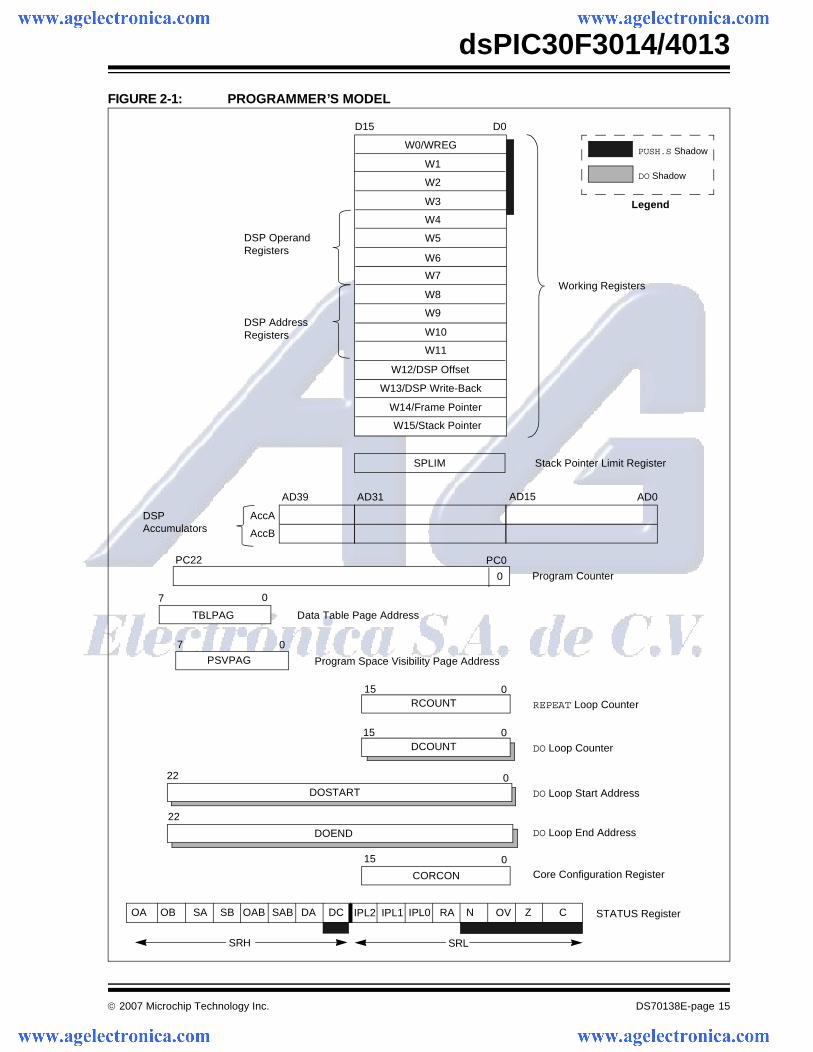
2.3 Divide Support
The dsPIC DSC devices feature a 16/16-bit signedfractional divide operation, as well as 32/16-bit and 16/16-bit signed and unsigned integer divide operations, inthe form of single instruction iterative divides. Thefollowing instructions and data sizes are supported:
1. DIVF – 16/16 signed fractional divide2. DIV.sd – 32/16 signed divide
3. DIV.ud – 32/16 unsigned divide4. DIV.s– 16/16 signed divide5. DIV.u – 16/16 unsigned divide
The 16/16 divides are similar to the 32/16 (same numberof iterations), but the dividend is either zero-extended orsign-extended during the first iteration.
The divide instructions must be executed within aREPEAT loop. Any other form of execution (e.g., aseries of discrete divide instructions) will not functioncorrectly because the instruction flow depends onRCOUNT. The divide instruction does not automaticallyset up the RCOUNT value and it must, therefore, beexplicitly and correctly specified in the REPEAT instruc-tion, as shown in Table 2-1 (REPEAT will execute thetarget instruction {operand value+1} times). TheREPEAT loop count must be setup for 18 iterations ofthe DIV/DIVF instruction. Thus, a complete divideoperation requires 19 cycles.
TABLE 2-1: DIVIDE INSTRUCTIONS
Note: The divide flow is interruptible. However,the user needs to save the context asappropriate.
Instruction Function
DIVF Signed fractional divide: Wm/Wn → W0; Rem → W1
DIV.sd Signed divide: (Wm+1:Wm)/Wn → W0; Rem → W1
DIV.s Signed divide: Wm/Wn → W0; Rem → W1
DIV.ud Unsigned divide: (Wm+1:Wm)/Wn → W0; Rem → W1
DIV.u Unsigned divide: Wm/Wn → W0; Rem → W1
© 2007 Microchip Technology Inc. DS70138E-page 17
dsPIC30F3014/4013
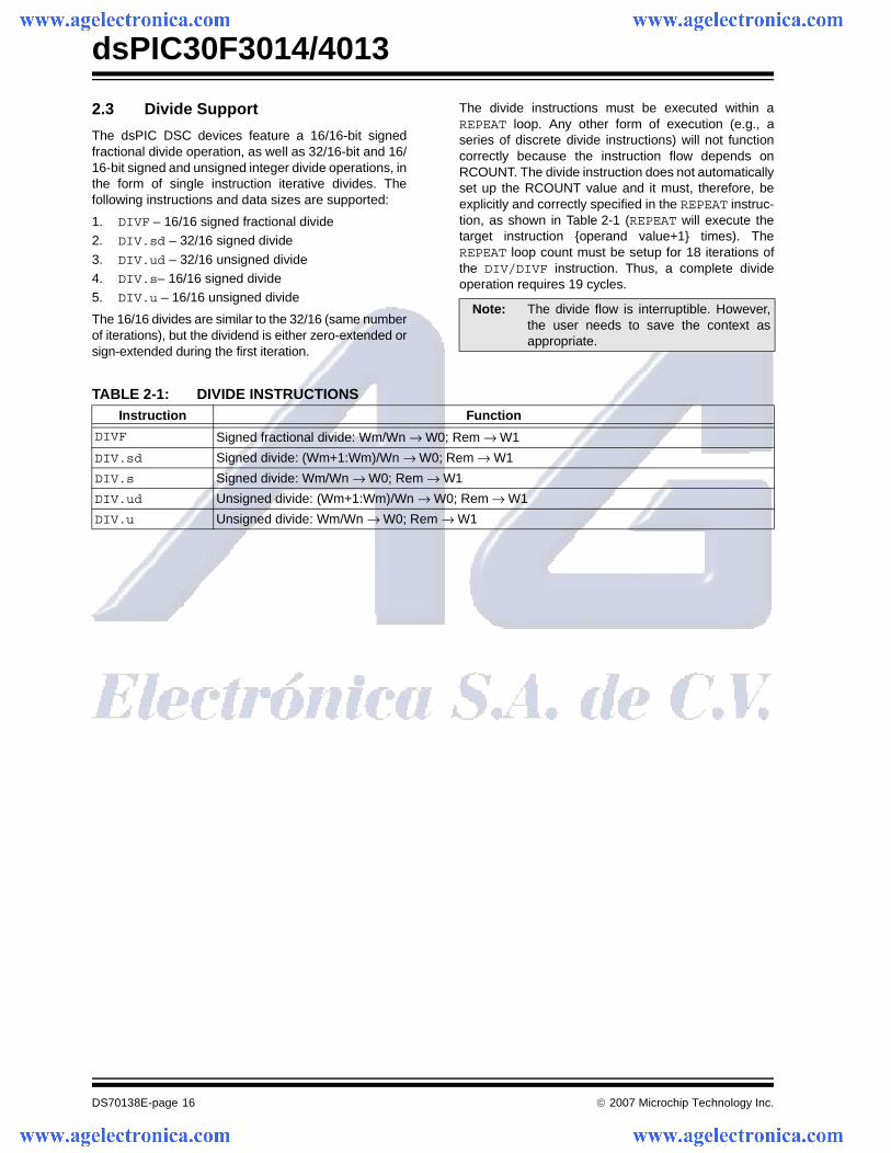
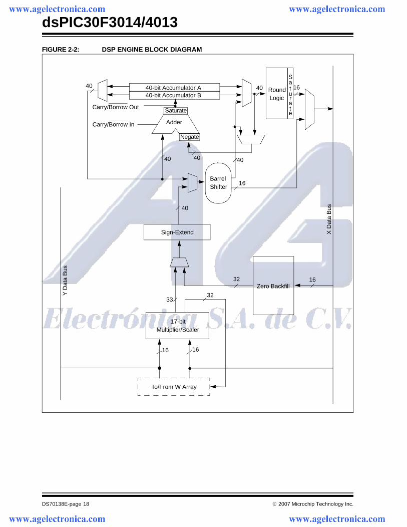
2.4 DSP Engine
The DSP engine consists of a high-speed, 17-bit x17-bit multiplier, a barrel shifter and a 40-bit adder/subtracter (with two target accumulators, round andsaturation logic).
The DSP engine also has the capability to performinherent accumulator-to-accumulator operations,which require no additional data. These instructions areADD, SUB and NEG.
The dsPIC30F is a single-cycle instruction flow archi-tecture, therefore, concurrent operation of the DSPengine with MCU instruction flow is not possible.However, some MCU ALU and DSP engine resourcesmay be used concurrently by the same instruction (e.g.,ED, EDAC). (See Table 2-2 for DSP instructions.)
The DSP engine has various options selected throughvarious bits in the CPU Core Configuration register(CORCON), as listed below:
1. Fractional or integer DSP multiply (IF).
2. Signed or unsigned DSP multiply (US).3. Conventional or convergent rounding (RND).4. Automatic saturation on/off for AccA (SATA).
5. Automatic saturation on/off for AccB (SATB).6. Automatic saturation on/off for writes to data
memory (SATDW).7. Accumulator Saturation mode selection
(ACCSAT).
A block diagram of the DSP engine is shown inFigure 2-2.
Note: For CORCON layout, see Table 3-3.
TABLE 2-2: DSP INSTRUCTION SUMMARY
Instruction Algebraic Operation ACC WB?
CLR A = 0 Yes
ED A = (x – y)2 No
EDAC A = A + (x – y)2 No
MAC A = A + (x * y) Yes
MAC A = A + x2 No
MOVSAC No change in A Yes
MPY A = x * y No
MPY.N A = – x * y No
MSC A = A – x * y Yes
dsPIC30F3014/4013
DS70138E-page 18 © 2007 Microchip Technology Inc.
FIGURE 2-2: DSP ENGINE BLOCK DIAGRAM
Zero Backfill
Sign-Extend
BarrelShifter
40-bit Accumulator A40-bit Accumulator B
RoundLogic
X D
ata
Bus
To/From W Array
Adder
Saturate
Negate
32
3233
16
16 16
16
40 40
40 40
Saturate
Y D
ata
Bus
40
Carry/Borrow Out
Carry/Borrow In
16
40
Multiplier/Scaler17-bit
© 2007 Microchip Technology Inc. DS70138E-page 19
dsPIC30F3014/4013
2.4.1 MULTIPLIER
The 17-bit x 17-bit multiplier is capable of signed orunsigned operation and can multiplex its output using ascaler to support either 1.31 fractional (Q31) or 32-bitinteger results. Unsigned operands are zero-extendedinto the 17th bit of the multiplier input value. Signedoperands are sign-extended into the 17th bit of themultiplier input value. The output of the 17-bit x 17-bitmultiplier/scaler is a 33-bit value, which is sign-extended to 40 bits. Integer data is inherently repre-sented as a signed two’s complement value, where theMSB is defined as a sign bit. Generally speaking, therange of an N-bit two’s complement integer is -2N-1 to2N-1 – 1. For a 16-bit integer, the data range is -32768(0x8000) to 32767 (0x7FFF) including ‘0’. For a 32-bitinteger, the data range is -2,147,483,648(0x8000 0000) to 2,147,483,645 (0x7FFF FFFF).
When the multiplier is configured for fractional multipli-cation, the data is represented as a two’s complementfraction, where the MSB is defined as a sign bit and theradix point is implied to lie just after the sign bit (QX for-mat). The range of an N-bit two’s complement fractionwith this implied radix point is -1.0 to (1 – 21-N). For a16-bit fraction, the Q15 data range is -1.0 (0x8000) to0.999969482 (0x7FFF) including ‘0’ and has a preci-sion of 3.01518x10⁻⁵. In Fractional mode, the 16x16multiply operation generates a 1.31 product, which hasa precision of 4.65661 x 10⁻¹⁰.
The same multiplier is used to support the MCU multi-ply instructions, which include integer 16-bit signed,unsigned and mixed sign multiplies.
The MUL instruction can be directed to use byte orword-sized operands. Byte operands direct a 16-bitresult, and word operands direct a 32-bit result to thespecified register(s) in the W array.
2.4.2 DATA ACCUMULATORS AND ADDER/SUBTRACTER
The data accumulator consists of a 40-bit adder/subtracter with automatic sign extension logic. It canselect one of two accumulators (A or B) as its pre-accumulation source and post-accumulation destina-tion. For the ADD and LAC instructions, the data to beaccumulated or loaded can be optionally scaled via thebarrel shifter prior to accumulation.
2.4.2.1 Adder/Subtracter, Overflow and Saturation
The adder/subtracter is a 40-bit adder with an optionalzero input into one side and either true or complementdata into the other input. In the case of addition, thecarry/borrow input is active high and the other input istrue data (not complemented), whereas in the case ofsubtraction, the carry/borrow input is active low and theother input is complemented. The adder/subtractergenerates overflow Status bits SA/SB and OA/OB,which are latched and reflected in the STATUS register:
• Overflow from bit 39: this is a catastrophic overflow in which the sign of the accumulator is destroyed.
• Overflow into guard bits 32 through 39: this is a recoverable overflow. This bit is set whenever all the guard bits are not identical to each other.
The adder has an additional saturation block whichcontrols accumulator data saturation if selected. It usesthe result of the adder, the overflow Status bitsdescribed above, and the SATA/B (CORCON<7:6>)and ACCSAT (CORCON<4>) mode control bits todetermine when and to what value to saturate.
Six STATUS register bits have been provided tosupport saturation and overflow. They are:
1. OA:AccA overflowed into guard bits
2. OB: AccB overflowed into guard bits
3. SA:AccA saturated (bit 31 overflow and saturation)orAccA overflowed into guard bits and saturated(bit 39 overflow and saturation)
4. SB:AccB saturated (bit 31 overflow and saturation)orAccB overflowed into guard bits and saturated(bit 39 overflow and saturation)
5. OAB:Logical OR of OA and OB
6. SAB:Logical OR of SA and SB
The OA and OB bits are modified each time datapasses through the adder/subtracter. When set, theyindicate that the most recent operation has overflowedinto the accumulator guard bits (bits 32 through 39).The OA and OB bits can also optionally generate anarithmetic warning trap when set and the correspond-ing overflow trap flag enable bit (OVATE, OVBTE) inthe INTCON1 register (refer to Section 8.0 “Inter-rupts”) is set. This allows the user to take immediateaction, for example, to correct system gain.
dsPIC30F3014/4013
DS70138E-page 20 © 2007 Microchip Technology Inc.
The SA and SB bits are modified each time datapasses through the adder/subtracter but can only becleared by the user. When set, they indicate that theaccumulator has overflowed its maximum range (bit 31for 32-bit saturation or bit 39 for 40-bit saturation) andwill be saturated if saturation is enabled. Whensaturation is not enabled, SA and SB default to bit 39overflow and, thus, indicate that a catastrophic over-flow has occurred. If the COVTE bit in the INTCON1register is set, SA and SB bits generate an arithmeticwarning trap when saturation is disabled.
The overflow and saturation Status bits can optionallybe viewed in the STATUS register (SR) as the logicalOR of OA and OB (in bit OAB) and the logical OR of SAand SB (in bit SAB). This allows programmers to checkone bit in the STATUS register to determine if eitheraccumulator has overflowed, or one bit to determine ifeither accumulator has saturated. This would be usefulfor complex number arithmetic which typically usesboth the accumulators.
The device supports three saturation and overflowmodes:
1. Bit 39 Overflow and Saturation:When bit 39 overflow and saturation occurs, thesaturation logic loads the maximally positive 9.31(0x7FFFFFFFFF), or maximally negative 9.31value (0x8000000000) into the target accumula-tor. The SA or SB bit is set and remains set untilcleared by the user. This is referred to as ‘supersaturation’ and provides protection against erro-neous data or unexpected algorithm problems(e.g., gain calculations).
2. Bit 31 Overflow and Saturation:When bit 31 overflow and saturation occurs, thesaturation logic then loads the maximally posi-tive 1.31 value (0x007FFFFFFF), or maximallynegative 1.31 value (0x0080000000) into thetarget accumulator. The SA or SB bit is set andremains set until cleared by the user. When thisSaturation mode is in effect, the guard bits arenot used, so the OA, OB or OAB bits are neverset.
3. Bit 39 Catastrophic Overflow:The bit 39 overflow Status bit from the adder isused to set the SA or SB bit which remain setuntil cleared by the user. No saturation operationis performed and the accumulator is allowed tooverflow (destroying its sign). If the COVTE bit inthe INTCON1 register is set, a catastrophicoverflow can initiate a trap exception.
2.4.2.2 Accumulator ‘Write-Back’
The MAC class of instructions (with the exception ofMPY, MPY.N, ED and EDAC) can optionally write arounded version of the high word (bits 31 through 16)of the accumulator that is not targeted by the instructioninto data space memory. The write is performed acrossthe X bus into combined X and Y address space. Thefollowing addressing modes are supported:
1. W13, Register Direct:The rounded contents of the non-targetaccumulator are written into W13 as a 1.15fraction.
2. [W13]+=2, Register Indirect with Post-Increment:The rounded contents of the non-target accumu-lator are written into the address pointed to byW13 as a 1.15 fraction. W13 is thenincremented by 2 (for a word write).
2.4.2.3 Round Logic
The round logic is a combinational block which per-forms a conventional (biased) or convergent (unbi-ased) round function during an accumulator write(store). The Round mode is determined by the state ofthe RND bit in the CORCON register. It generates a 16-bit, 1.15 data value, which is passed to the data spacewrite saturation logic. If rounding is not indicated by theinstruction, a truncated 1.15 data value is stored andthe least significant word (lsw) is simply discarded.
Conventional rounding takes bit 15 of the accumulator,zero-extends it and adds it to the ACCxH word (bits 16through 31 of the accumulator). If the ACCxL word(bits 0 through 15 of the accumulator) is between0x8000 and 0xFFFF (0x8000 included), ACCxH isincremented. If ACCxL is between 0x0000 and 0x7FFF,ACCxH is left unchanged. A consequence of this algo-rithm is that over a succession of random roundingoperations, the value tends to be biased slightly posi-tive.
Convergent (or unbiased) rounding operates in thesame manner as conventional rounding, except whenACCxL equals 0x8000. If this is the case, the Least Sig-nificant bit (LSb) (bit 16 of the accumulator) of ACCxHis examined. If it is ‘1’, ACCxH is incremented. If it is ‘0’,ACCxH is not modified. Assuming that bit 16 iseffectively random in nature, this scheme removes anyrounding bias that may accumulate.
The SAC and SAC.R instructions store either a trun-cated (SAC) or rounded (SAC.R) version of the contentsof the target accumulator to data memory via the X bus(subject to data saturation, see Section 2.4.2.4 “DataSpace Write Saturation”). Note that for the MAC classof instructions, the accumulator write-back operationfunctions in the same manner, addressing combinedMCU (X and Y) data space though the X bus. For thisclass of instructions, the data is always subject torounding.
© 2007 Microchip Technology Inc. DS70138E-page 21
dsPIC30F3014/4013
2.4.2.4 Data Space Write Saturation
In addition to adder/subtracter saturation, writes to dataspace may also be saturated but without affecting thecontents of the source accumulator. The data spacewrite saturation logic block accepts a 16-bit, 1.15fractional value from the round logic block as its input,together with overflow status from the original source(accumulator) and the 16-bit round adder. These arecombined and used to select the appropriate 1.15fractional value as output to write to data spacememory.
If the SATDW bit in the CORCON register is set, data(after rounding or truncation) is tested for overflow andadjusted accordingly. For input data greater than0x007FFF, data written to memory is forced to themaximum positive 1.15 value, 0x7FFF. For input dataless than 0xFF8000, data written to memory is forcedto the maximum negative 1.15 value, 0x8000. TheMost Significant bit (MSb) of the source (bit 39) is usedto determine the sign of the operand being tested.
If the SATDW bit in the CORCON register is not set, theinput data is always passed through unmodified underall conditions.
2.4.3 BARREL SHIFTER
The barrel shifter is capable of performing up to 16-bitarithmetic or logic right shifts, or up to 16-bit left shiftsin a single cycle. The source can be either of the twoDSP accumulators, or the X bus (to support multi-bitshifts of register or memory data).
The shifter requires a signed binary value to determineboth the magnitude (number of bits) and direction of theshift operation. A positive value shifts the operand right.A negative value shifts the operand left. A value of ‘0’does not modify the operand.
The barrel shifter is 40 bits wide, thereby obtaining a40-bit result for DSP shift operations and a 16-bit resultfor MCU shift operations. Data from the X bus ispresented to the barrel shifter between bit positions 16to 31 for right shifts, and bit positions 0 to 16 for leftshifts.

dsPIC30F3014/4013
DS70138E-page 22 © 2007 Microchip Technology Inc.
NOTES:
© 2007 Microchip Technology Inc. DS70138E-page 23
dsPIC30F3014/4013
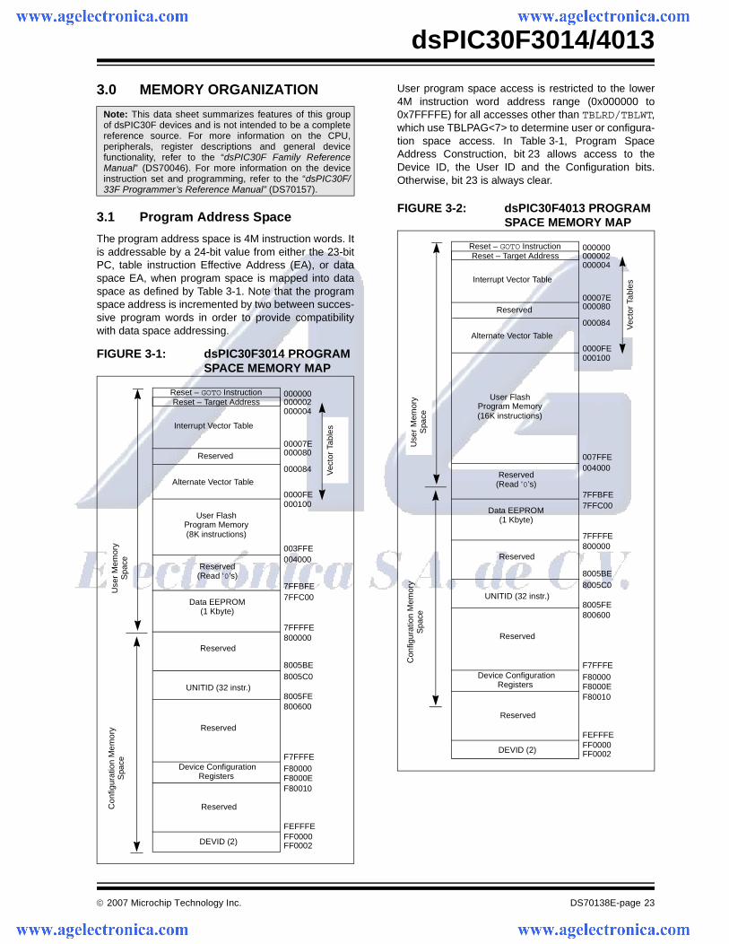
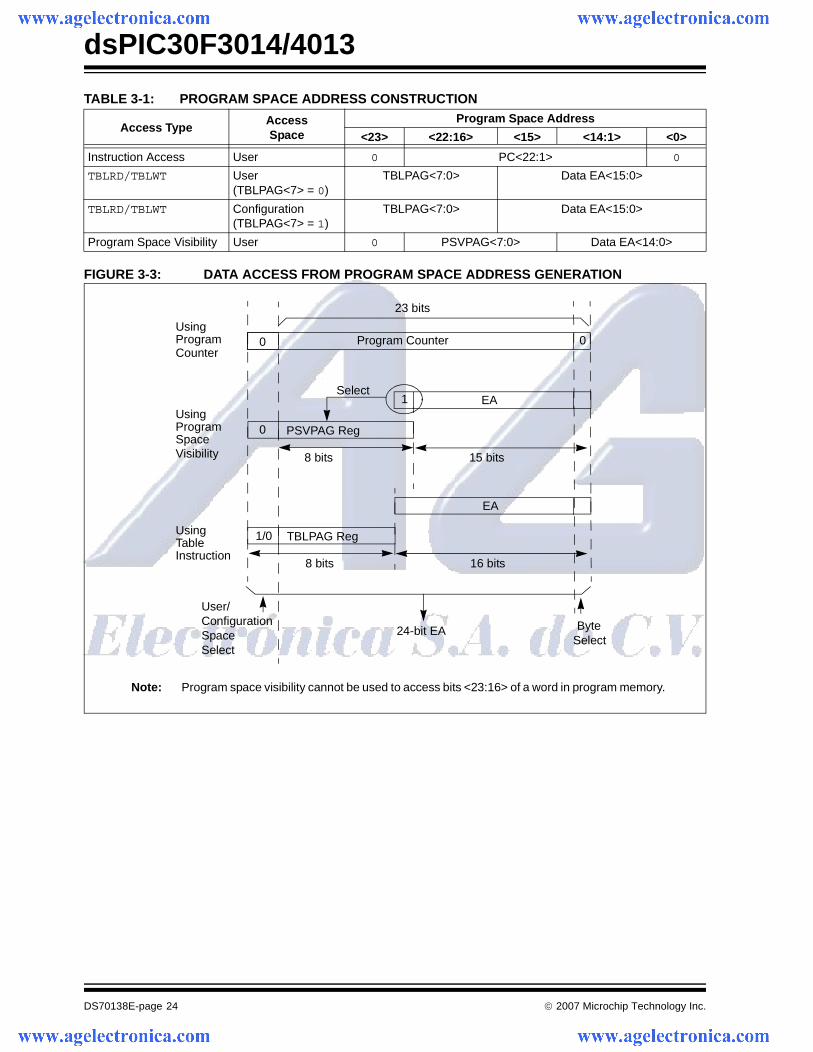
3.0 MEMORY ORGANIZATION
3.1 Program Address Space
The program address space is 4M instruction words. Itis addressable by a 24-bit value from either the 23-bitPC, table instruction Effective Address (EA), or dataspace EA, when program space is mapped into dataspace as defined by Table 3-1. Note that the programspace address is incremented by two between succes-sive program words in order to provide compatibilitywith data space addressing.
FIGURE 3-1: dsPIC30F3014 PROGRAM SPACE MEMORY MAP
User program space access is restricted to the lower4M instruction word address range (0x000000 to0x7FFFFE) for all accesses other than TBLRD/TBLWT,which use TBLPAG<7> to determine user or configura-tion space access. In Table 3-1, Program SpaceAddress Construction, bit 23 allows access to theDevice ID, the User ID and the Configuration bits.Otherwise, bit 23 is always clear.
FIGURE 3-2: dsPIC30F4013 PROGRAM SPACE MEMORY MAP
Note: This data sheet summarizes features of this groupof dsPIC30F devices and is not intended to be a completereference source. For more information on the CPU,peripherals, register descriptions and general devicefunctionality, refer to the “dsPIC30F Family ReferenceManual” (DS70046). For more information on the deviceinstruction set and programming, refer to the “dsPIC30F/33F Programmer’s Reference Manual” (DS70157).
Reset – Target Address
Use
r M
emor
yS
pace
User FlashProgram Memory
Con
figur
atio
n M
emor
yS
pace
(8K instructions)
Reset – GOTO Instruction
Alternate Vector Table
Reserved
Interrupt Vector Table
Vec
tor
Tabl
es
000000
00007E
000002
000080
Device Configuration
004000003FFE
Data EEPROM(1 Kbyte)
800000
F80000Registers F8000E
F80010
DEVID (2)
FEFFFEFF0000FF0002
Reserved
F7FFFE
Reserved
7FFC007FFBFE
(Read ‘0’s)
8005FE800600
UNITID (32 instr.)
8005BE8005C0
000004
Reserved
7FFFFE
Reserved
0001000000FE
000084
Reset – Target Address
Use
r M
emor
yS
pace
000000
00007E
000002
000080
Device Configuration
User FlashProgram Memory
004000007FFE
Con
figur
atio
n M
emor
yS
pace
Data EEPROM
(16K instructions)
(1 Kbyte)
800000
F80000Registers F8000E
F80010
DEVID (2)
FEFFFEFF0000FF0002
Reserved
F7FFFE
Reserved
7FFC007FFBFE
(Read ‘0’s)
8005FE800600
UNITID (32 instr.)
8005BE8005C0
Reset – GOTO Instruction
000004
Reserved
7FFFFE
Reserved
0001000000FE
000084
Alternate Vector Table
Reserved
Interrupt Vector Table
Vec
tor
Tabl
es
dsPIC30F3014/4013
DS70138E-page 24 © 2007 Microchip Technology Inc.
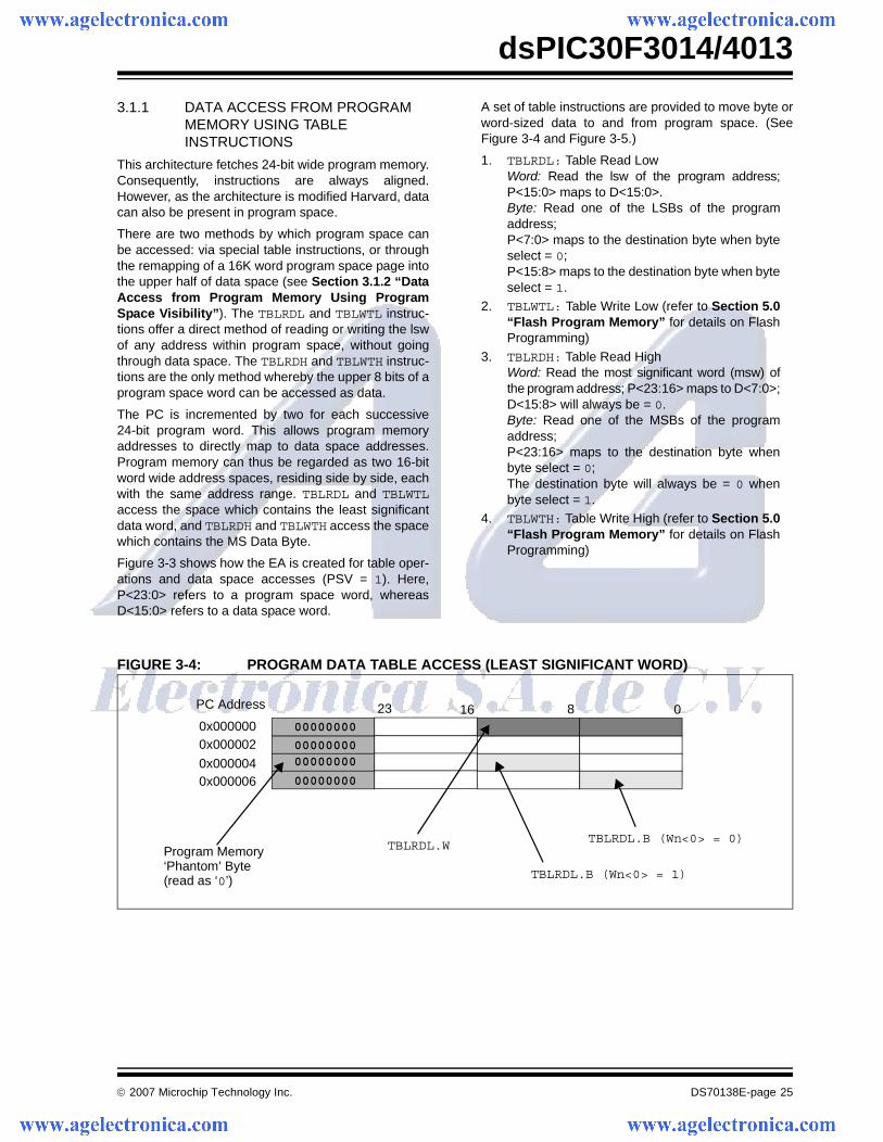
TABLE 3-1: PROGRAM SPACE ADDRESS CONSTRUCTION
FIGURE 3-3: DATA ACCESS FROM PROGRAM SPACE ADDRESS GENERATION
Access TypeAccessSpace
Program Space Address
<23> <22:16> <15> <14:1> <0>
Instruction Access User 0 PC<22:1> 0
TBLRD/TBLWT User (TBLPAG<7> = 0)
TBLPAG<7:0> Data EA<15:0>
TBLRD/TBLWT Configuration (TBLPAG<7> = 1)
TBLPAG<7:0> Data EA<15:0>
Program Space Visibility User 0 PSVPAG<7:0> Data EA<14:0>
0Program Counter
23 bits
1
PSVPAG Reg
8 bits
EA
15 bits
Program
Using
Select
TBLPAG Reg
8 bits
EA
16 bits
Using
Byte24-bit EA
0
0
1/0
Select
User/Configuration
TableInstruction
ProgramSpace
Counter
Using
SpaceSelect
Visibility
Note: Program space visibility cannot be used to access bits <23:16> of a word in program memory.
© 2007 Microchip Technology Inc. DS70138E-page 25
dsPIC30F3014/4013
3.1.1 DATA ACCESS FROM PROGRAM MEMORY USING TABLE INSTRUCTIONS
This architecture fetches 24-bit wide program memory.Consequently, instructions are always aligned.However, as the architecture is modified Harvard, datacan also be present in program space.
There are two methods by which program space canbe accessed: via special table instructions, or throughthe remapping of a 16K word program space page intothe upper half of data space (see Section 3.1.2 “DataAccess from Program Memory Using ProgramSpace Visibility”). The TBLRDL and TBLWTL instruc-tions offer a direct method of reading or writing the lswof any address within program space, without goingthrough data space. The TBLRDH and TBLWTH instruc-tions are the only method whereby the upper 8 bits of aprogram space word can be accessed as data.
The PC is incremented by two for each successive24-bit program word. This allows program memoryaddresses to directly map to data space addresses.Program memory can thus be regarded as two 16-bitword wide address spaces, residing side by side, eachwith the same address range. TBLRDL and TBLWTLaccess the space which contains the least significantdata word, and TBLRDH and TBLWTH access the spacewhich contains the MS Data Byte.
Figure 3-3 shows how the EA is created for table oper-ations and data space accesses (PSV = 1). Here,P<23:0> refers to a program space word, whereasD<15:0> refers to a data space word.
A set of table instructions are provided to move byte orword-sized data to and from program space. (SeeFigure 3-4 and Figure 3-5.)
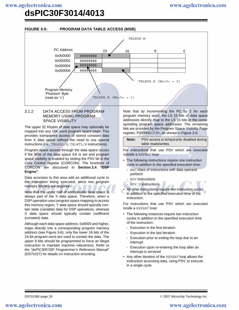
1. TBLRDL: Table Read LowWord: Read the lsw of the program address;P<15:0> maps to D<15:0>.Byte: Read one of the LSBs of the programaddress;P<7:0> maps to the destination byte when byteselect = 0;P<15:8> maps to the destination byte when byteselect = 1.
2. TBLWTL: Table Write Low (refer to Section 5.0“Flash Program Memory” for details on FlashProgramming)
3. TBLRDH: Table Read HighWord: Read the most significant word (msw) ofthe program address; P<23:16> maps to D<7:0>;D<15:8> will always be = 0.Byte: Read one of the MSBs of the programaddress;P<23:16> maps to the destination byte whenbyte select = 0;The destination byte will always be = 0 whenbyte select = 1.
4. TBLWTH: Table Write High (refer to Section 5.0“Flash Program Memory” for details on FlashProgramming)
FIGURE 3-4: PROGRAM DATA TABLE ACCESS (LEAST SIGNIFICANT WORD)
0816PC Address
0x0000000x000002
0x0000040x000006
2300000000
00000000
00000000
00000000
Program Memory‘Phantom’ Byte(read as ‘0’)
TBLRDL.W
TBLRDL.B (Wn<0> = 1)
TBLRDL.B (Wn<0> = 0)
dsPIC30F3014/4013
DS70138E-page 26 © 2007 Microchip Technology Inc.
FIGURE 3-5: PROGRAM DATA TABLE ACCESS (MSB)
3.1.2 DATA ACCESS FROM PROGRAM MEMORY USING PROGRAM SPACE VISIBILITY
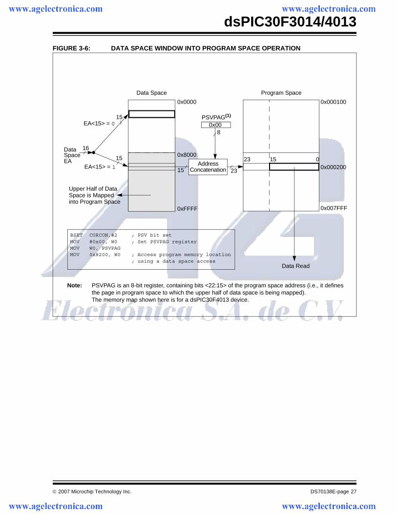
The upper 32 Kbytes of data space may optionally bemapped into any 16K word program space page. Thisprovides transparent access of stored constant datafrom X data space without the need to use specialinstructions (i.e., TBLRDL/H, TBLWTL/H instructions).
Program space access through the data space occursif the MSb of the data space EA is set and programspace visibility is enabled by setting the PSV bit in theCore Control register (CORCON). The functions ofCORCON are discussed in Section 2.4 “DSPEngine”.
Data accesses to this area add an additional cycle tothe instruction being executed, since two programmemory fetches are required.
Note that the upper half of addressable data space isalways part of the X data space. Therefore, when aDSP operation uses program space mapping to accessthis memory region, Y data space should typically con-tain state (variable) data for DSP operations, whereasX data space should typically contain coefficient(constant) data.
Although each data space address, 0x8000 and higher,maps directly into a corresponding program memoryaddress (see Figure 3-6), only the lower 16 bits of the24-bit program word are used to contain the data. Theupper 8 bits should be programmed to force an illegalinstruction to maintain machine robustness. Refer tothe “dsPIC30F/33F Programmer’s Reference Manual”(DS70157) for details on instruction encoding.
Note that by incrementing the PC by 2 for eachprogram memory word, the LS 15 bits of data spaceaddresses directly map to the LS 15 bits in the corre-sponding program space addresses. The remainingbits are provided by the Program Space Visibility Pageregister, PSVPAG<7:0>, as shown in Figure 3-6.
For instructions that use PSV which are executedoutside a REPEAT loop:
• The following instructions require one instruction cycle in addition to the specified execution time: - MAC class of instructions with data operand
prefetch- MOV instructions- MOV.D instructions
• All other instructions require two instruction cycles in addition to the specified execution time of the instruction.
For instructions that use PSV which are executedinside a REPEAT loop:
• The following instances require two instruction cycles in addition to the specified execution time of the instruction:- Execution in the first iteration
- Execution in the last iteration- Execution prior to exiting the loop due to an
interrupt- Execution upon re-entering the loop after an
interrupt is serviced• Any other iteration of the REPEAT loop allows the
instruction accessing data, using PSV, to execute in a single cycle.
0816PC Address
0x0000000x000002
0x0000040x000006
2300000000
00000000
00000000
00000000
Program Memory‘Phantom’ Byte(read as ‘0’)
TBLRDH.W
TBLRDH.B (Wn<0> = 1)
TBLRDH.B (Wn<0> = 0)
Note: PSV access is temporarily disabled duringtable reads/writes.
© 2007 Microchip Technology Inc. DS70138E-page 27
dsPIC30F3014/4013
FIGURE 3-6: DATA SPACE WINDOW INTO PROGRAM SPACE OPERATION
23 15 0
PSVPAG(1)15
15
EA<15> = 0
EA<15> = 1
16DataSpaceEA
Data Space Program Space
8
15 23
0x0000
0x8000
0xFFFF
0x00
0x000100
0x007FFF
Data Read
Upper Half of Data Space is Mapped into Program Space
0x000200Address
Concatenation
BSET CORCON,#2 ; PSV bit setMOV #0x00, W0 ; Set PSVPAG registerMOV W0, PSVPAGMOV 0x8200, W0 ; Access program memory location
; using a data space access
Note: PSVPAG is an 8-bit register, containing bits <22:15> of the program space address (i.e., it definesthe page in program space to which the upper half of data space is being mapped).The memory map shown here is for a dsPIC30F4013 device.
dsPIC30F3014/4013
DS70138E-page 28 © 2007 Microchip Technology Inc.
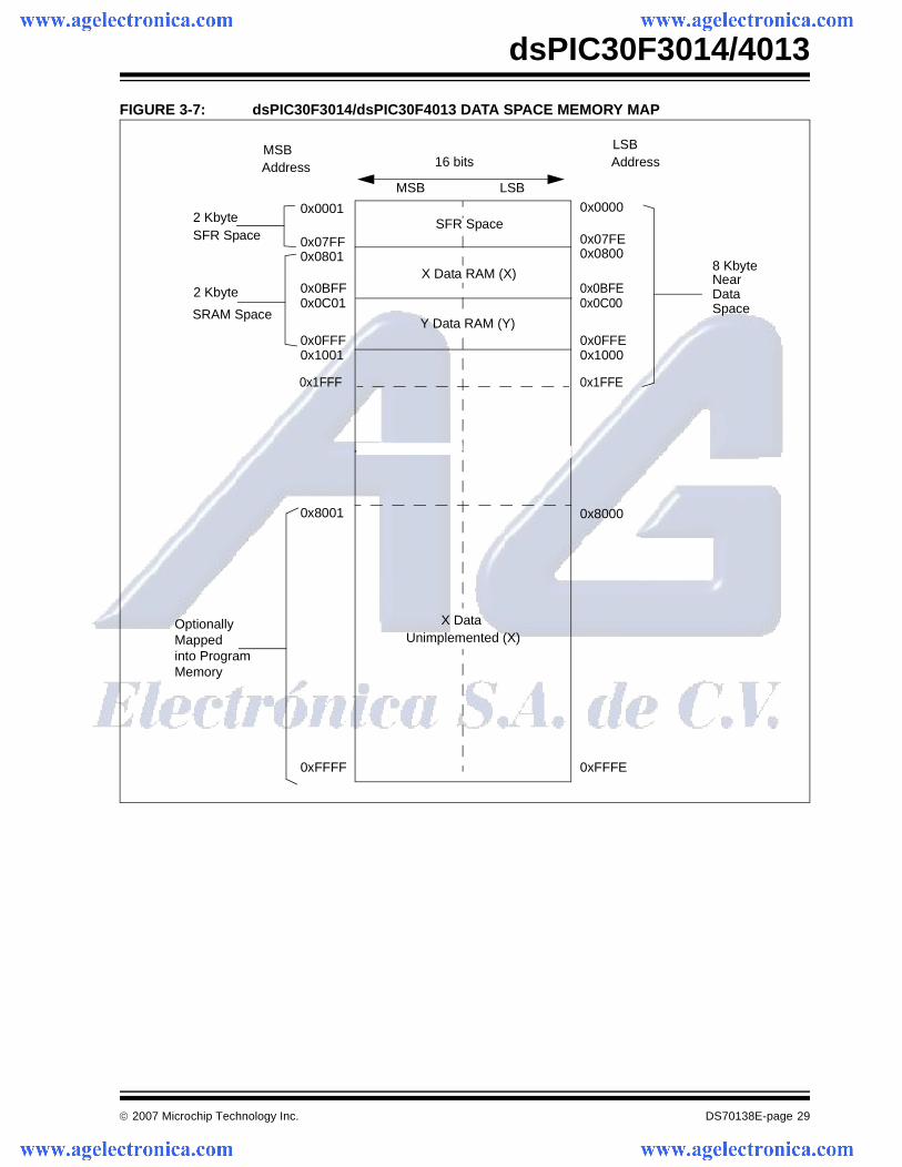
3.2 Data Address Space
The core has two data spaces. The data spaces can beconsidered either separate (for some DSP instruc-tions), or as one unified linear address range (for MCUinstructions). The data spaces are accessed using twoAddress Generation Units (AGUs) and separate datapaths.
3.2.1 DATA SPACE MEMORY MAP
The data space memory is split into two blocks, X andY data space. A key element of this architecture is thatY space is a subset of X space, and is fully containedwithin X space. In order to provide an apparent LinearAddressing space, X and Y spaces have contiguousaddresses.
When executing any instruction other than one of theMAC class of instructions, the X block consists of the 64-Kbyte data address space (including all Y addresses).When executing one of the MAC class of instructions,the X block consists of the 64-Kbyte data addressspace excluding the Y address block (for data readsonly). In other words, all other instructions regard theentire data memory as one composite address space.The MAC class instructions extract the Y address spacefrom data space and address it using EAs sourced fromW10 and W11. The remaining X data space isaddressed using W8 and W9. Both address spaces areconcurrently accessed only with the MAC classinstructions.
The data space memory map is shown in Figure 3-7.
© 2007 Microchip Technology Inc. DS70138E-page 29
dsPIC30F3014/4013
FIGURE 3-7: dsPIC30F3014/dsPIC30F4013 DATA SPACE MEMORY MAP
0x0000
0x07FE
0x0BFE
0xFFFE
LSBAddress16 bits
LSBMSB
MSBAddress
0x0001
0x07FF
0x0BFF
0xFFFF
0x8001 0x8000
OptionallyMappedinto ProgramMemory
0x0FFF 0x0FFE0x10000x1001
0x0801 0x0800
0x0C01 0x0C00
NearData
0x1FFE 0x1FFF
2 KbyteSFR Space
2 Kbyte
SRAM Space
8 Kbyte
Space
X Data Unimplemented (X)
SFR Space
X Data RAM (X)
Y Data RAM (Y)
dsPIC30F3014/4013
DS70138E-page 30 © 2007 Microchip Technology Inc.
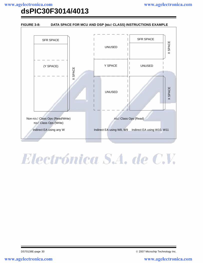
FIGURE 3-8: DATA SPACE FOR MCU AND DSP (MAC CLASS) INSTRUCTIONS EXAMPLE
SFR SPACE
(Y SPACE)
X S
PA
CE
SFR SPACE
UNUSED
X S
PA
CE
X S
PA
CE
Y SPACE
UNUSED
UNUSED
Non-MAC Class Ops (Read/Write) MAC Class Ops (Read)
Indirect EA using any W Indirect EA using W8, W9 Indirect EA using W10, W11
MAC Class Ops (Write)
© 2007 Microchip Technology Inc. DS70138E-page 31
dsPIC30F3014/4013
3.2.2 DATA SPACES
The X data space is used by all instructions and sup-ports all addressing modes. There are separate readand write data buses. The X read data bus is the returndata path for all instructions that view data space ascombined X and Y address space. It is also the Xaddress space data path for the dual operand readinstructions (MAC class). The X write data bus is theonly write path to data space for all instructions.
The X data space also supports Modulo Addressing forall instructions, subject to addressing mode restric-tions. Bit-Reversed Addressing is only supported forwrites to X data space.
The Y data space is used in concert with the X dataspace by the MAC class of instructions (CLR, ED,EDAC, MAC, MOVSAC, MPY, MPY.N and MSC) toprovide two concurrent data read paths. No writesoccur across the Y bus. This class of instructions dedi-cates two W register pointers, W10 and W11, to alwaysaddress Y data space, independent of X data space,whereas W8 and W9 always address X data space.Note that during accumulator write-back, the dataaddress space is considered a combination of X and Ydata spaces, so the write occurs across the X bus.Consequently, the write can be to any address in theentire data space.
The Y data space can only be used for the dataprefetch operation associated with the MAC class ofinstructions. It also supports Modulo Addressing forautomated circular buffers. Of course, all other instruc-tions can access the Y data address space through theX data path as part of the composite linear space.
The boundary between the X and Y data spaces isdefined as shown in Figure 3-7 and is not user pro-grammable. Should an EA point to data outside its ownassigned address space, or to a location outside phys-ical memory, an all zero word/byte is returned. Forexample, although Y address space is visible by allnon-MAC instructions using any addressing mode, anattempt by a MAC instruction to fetch data from thatspace using W8 or W9 (X space pointers) returns0x0000.
TABLE 3-2: EFFECT OF INVALID MEMORY ACCESSES
All Effective Addresses are 16 bits wide and point tobytes within the data space. Therefore, the data spaceaddress range is 64 Kbytes or 32K words.
3.2.3 DATA SPACE WIDTH
The core data width is 16 bits. All internal registers areorganized as 16-bit wide words. Data space memory isorganized in byte addressable, 16-bit wide blocks.
3.2.4 DATA ALIGNMENT
To help maintain backward compatibility with PIC®
MCU devices and improve data space memory usageefficiency, the dsPIC30F instruction set supports bothword and byte operations. Data is aligned in data mem-ory and registers as words, but all data space EAsresolve to bytes. Data byte reads read the completeword which contains the byte, using the LSb of any EAto determine which byte to select. The selected byte isplaced onto the LSB of the X data path (no byteaccesses are possible from the Y data path as the MACclass of instruction can only fetch words). That is, datamemory and registers are organized as two parallelbyte-wide entities with shared (word) address decodebut separate write lines. Data byte writes only write tothe corresponding side of the array or register whichmatches the byte address.
As a consequence of this byte accessibility, all EffectiveAddress calculations (including those generated by theDSP operations which are restricted to word-sizeddata) are internally scaled to step through word alignedmemory. For example, the core would recognize thatPost-Modified Register Indirect Addressing mode[Ws++] will result in a value of Ws + 1 for byteoperations and Ws + 2 for word operations.
All word accesses must be aligned to an even address.Misaligned word data fetches are not supported socare must be taken when mixing byte and word opera-tions, or translating from 8-bit MCU code. Should a mis-aligned read or write be attempted, an address errortrap is generated. If the error occurred on a read, theinstruction underway is completed, whereas if itoccurred on a write, the instruction is executed but thewrite does not occur. In either case, a trap is then exe-cuted, allowing the system and/or user to examine themachine state prior to execution of the address Fault.
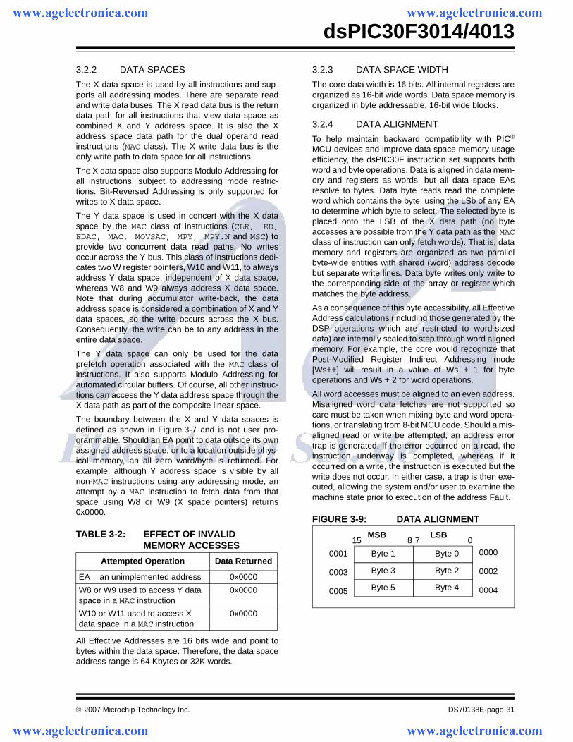
FIGURE 3-9: DATA ALIGNMENT
Attempted Operation Data Returned
EA = an unimplemented address 0x0000
W8 or W9 used to access Y data space in a MAC instruction
0x0000
W10 or W11 used to access X data space in a MAC instruction
0x0000
15 8 7 0
0001
0003
0005
0000
0002
0004
Byte 1 Byte 0
Byte 3 Byte 2
Byte 5 Byte 4
LSBMSB
dsPIC30F3014/4013
DS70138E-page 32 © 2007 Microchip Technology Inc.
All byte loads into any W register are loaded into theLSB. The MSB is not modified.
A Sign-Extend (SE) instruction is provided to allowusers to translate 8-bit signed data to 16-bit signedvalues. Alternatively, for 16-bit unsigned data, userscan clear the MSB of any W register by executing aZero-Extend (ZE) instruction on the appropriateaddress.
Although most instructions are capable of operating onword or byte data sizes, it should be noted that someinstructions, including the DSP instructions, operateonly on words.
3.2.5 NEAR DATA SPACE
An 8-Kbyte ‘near’ data space is reserved in X addressmemory space between 0x0000 and 0x1FFF, which isdirectly addressable via a 13-bit absolute address fieldwithin all memory direct instructions. The remaining Xaddress space and all of the Y address space isaddressable indirectly. Additionally, the whole of X dataspace is addressable using MOV instructions, whichsupport memory direct addressing with a 16-bitaddress field.
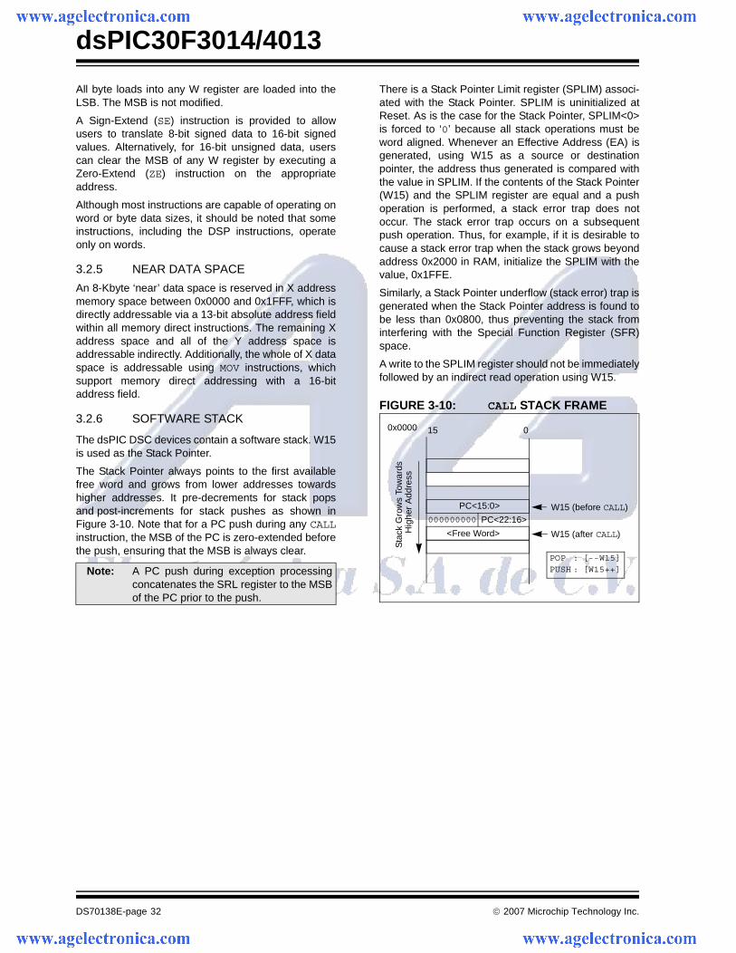
3.2.6 SOFTWARE STACK
The dsPIC DSC devices contain a software stack. W15is used as the Stack Pointer.
The Stack Pointer always points to the first availablefree word and grows from lower addresses towardshigher addresses. It pre-decrements for stack popsand post-increments for stack pushes as shown inFigure 3-10. Note that for a PC push during any CALLinstruction, the MSB of the PC is zero-extended beforethe push, ensuring that the MSB is always clear.
There is a Stack Pointer Limit register (SPLIM) associ-ated with the Stack Pointer. SPLIM is uninitialized atReset. As is the case for the Stack Pointer, SPLIM<0>is forced to ‘0’ because all stack operations must beword aligned. Whenever an Effective Address (EA) isgenerated, using W15 as a source or destinationpointer, the address thus generated is compared withthe value in SPLIM. If the contents of the Stack Pointer(W15) and the SPLIM register are equal and a pushoperation is performed, a stack error trap does notoccur. The stack error trap occurs on a subsequentpush operation. Thus, for example, if it is desirable tocause a stack error trap when the stack grows beyondaddress 0x2000 in RAM, initialize the SPLIM with thevalue, 0x1FFE.
Similarly, a Stack Pointer underflow (stack error) trap isgenerated when the Stack Pointer address is found tobe less than 0x0800, thus preventing the stack frominterfering with the Special Function Register (SFR)space.
A write to the SPLIM register should not be immediatelyfollowed by an indirect read operation using W15.
FIGURE 3-10: CALL STACK FRAME
Note: A PC push during exception processingconcatenates the SRL register to the MSBof the PC prior to the push.
<Free Word>
PC<15:0>
000000000
015
W15 (before CALL)
W15 (after CALL)
Sta
ck G
row
s To
war
dsH
ighe
r A
ddre
ss
0x0000
PC<22:16>
POP : [--W15]PUSH : [W15++]
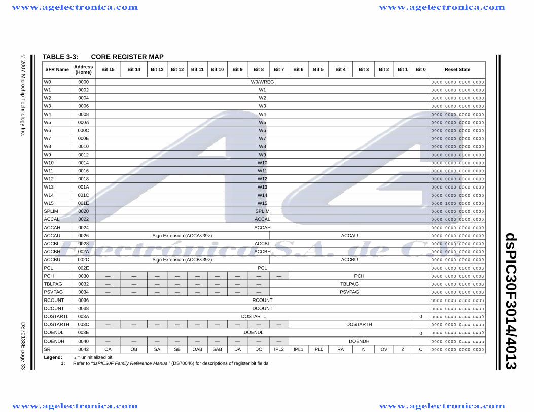
© 2007 M
icrochip Technology Inc.
DS
70138E-page 33
dsP
IC30F
3014/4013
TABLE 3-3: CORE REGISTER MAP
SFR Name Address(Home) Bit 15 Bit 14 Bit 13 Bit 12 Bit 11 Bit 10 Bit 9 Bit 8 Bit 7 Bit 6 Bit 5 Bit 4 Bit 3 Bit 2 Bit 1 Bit 0 Reset State
W0 0000 W0/WREG 0000 0000 0000 0000
W1 0002 W1 0000 0000 0000 0000
W2 0004 W2 0000 0000 0000 0000
W3 0006 W3 0000 0000 0000 0000
W4 0008 W4 0000 0000 0000 0000
W5 000A W5 0000 0000 0000 0000
W6 000C W6 0000 0000 0000 0000
W7 000E W7 0000 0000 0000 0000
W8 0010 W8 0000 0000 0000 0000
W9 0012 W9 0000 0000 0000 0000
W10 0014 W10 0000 0000 0000 0000
W11 0016 W11 0000 0000 0000 0000
W12 0018 W12 0000 0000 0000 0000
W13 001A W13 0000 0000 0000 0000
W14 001C W14 0000 0000 0000 0000
W15 001E W15 0000 1000 0000 0000
SPLIM 0020 SPLIM 0000 0000 0000 0000
ACCAL 0022 ACCAL 0000 0000 0000 0000
ACCAH 0024 ACCAH 0000 0000 0000 0000
ACCAU 0026 Sign Extension (ACCA<39>) ACCAU 0000 0000 0000 0000
ACCBL 0028 ACCBL 0000 0000 0000 0000
ACCBH 002A ACCBH 0000 0000 0000 0000
ACCBU 002C Sign Extension (ACCB<39>) ACCBU 0000 0000 0000 0000
PCL 002E PCL 0000 0000 0000 0000
PCH 0030 — — — — — — — — — PCH 0000 0000 0000 0000
TBLPAG 0032 — — — — — — — — TBLPAG 0000 0000 0000 0000
PSVPAG 0034 — — — — — — — — PSVPAG 0000 0000 0000 0000
RCOUNT 0036 RCOUNT uuuu uuuu uuuu uuuu
DCOUNT 0038 DCOUNT uuuu uuuu uuuu uuuu
DOSTARTL 003A DOSTARTL 0 uuuu uuuu uuuu uuu0
DOSTARTH 003C — — — — — — — — — DOSTARTH 0000 0000 0uuu uuuu
DOENDL 003E DOENDL 0 uuuu uuuu uuuu uuu0
DOENDH 0040 — — — — — — — — — DOENDH 0000 0000 0uuu uuuu
SR 0042 OA OB SA SB OAB SAB DA DC IPL2 IPL1 IPL0 RA N OV Z C 0000 0000 0000 0000
Legend: u = uninitialized bit1: Refer to “dsPIC30F Family Reference Manual” (DS70046) for descriptions of register bit fields.
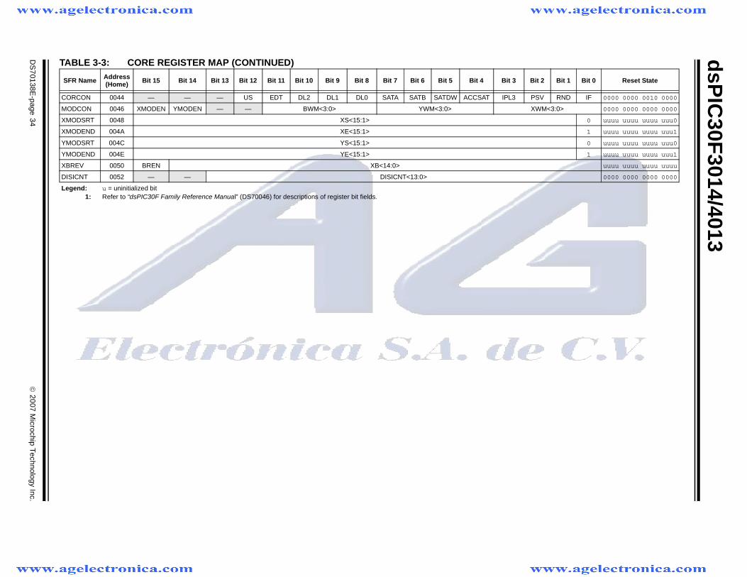
dsP
IC30F
3014/4013
DS
70138E-page 34
© 2007 M
icrochip Technology Inc.
CORCON 0044 — — — US EDT DL2 DL1 DL0 SATA SATB SATDW ACCSAT IPL3 PSV RND IF 0000 0000 0010 0000
MODCON 0046 XMODEN YMODEN — — BWM<3:0> YWM<3:0> XWM<3:0> 0000 0000 0000 0000
XMODSRT 0048 XS<15:1> 0 uuuu uuuu uuuu uuu0
XMODEND 004A XE<15:1> 1 uuuu uuuu uuuu uuu1
YMODSRT 004C YS<15:1> 0 uuuu uuuu uuuu uuu0
YMODEND 004E YE<15:1> 1 uuuu uuuu uuuu uuu1
XBREV 0050 BREN XB<14:0> uuuu uuuu uuuu uuuu
DISICNT 0052 — — DISICNT<13:0> 0000 0000 0000 0000
TABLE 3-3: CORE REGISTER MAP (CONTINUED)
SFR Name Address(Home) Bit 15 Bit 14 Bit 13 Bit 12 Bit 11 Bit 10 Bit 9 Bit 8 Bit 7 Bit 6 Bit 5 Bit 4 Bit 3 Bit 2 Bit 1 Bit 0 Reset State
Legend: u = uninitialized bit1: Refer to “dsPIC30F Family Reference Manual” (DS70046) for descriptions of register bit fields.
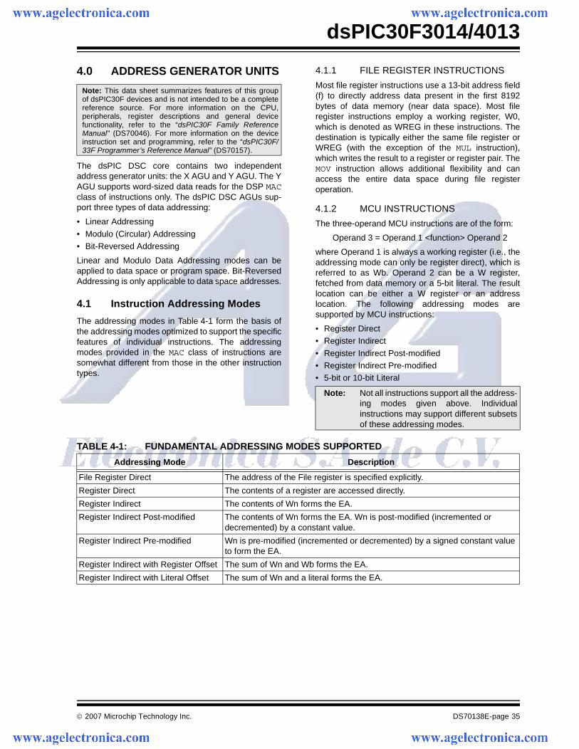
© 2007 Microchip Technology Inc. DS70138E-page 35
dsPIC30F3014/4013
4.0 ADDRESS GENERATOR UNITS
The dsPIC DSC core contains two independentaddress generator units: the X AGU and Y AGU. The YAGU supports word-sized data reads for the DSP MACclass of instructions only. The dsPIC DSC AGUs sup-port three types of data addressing:
• Linear Addressing
• Modulo (Circular) Addressing• Bit-Reversed Addressing
Linear and Modulo Data Addressing modes can beapplied to data space or program space. Bit-ReversedAddressing is only applicable to data space addresses.
4.1 Instruction Addressing Modes
The addressing modes in Table 4-1 form the basis ofthe addressing modes optimized to support the specificfeatures of individual instructions. The addressingmodes provided in the MAC class of instructions aresomewhat different from those in the other instructiontypes.
4.1.1 FILE REGISTER INSTRUCTIONS
Most file register instructions use a 13-bit address field(f) to directly address data present in the first 8192bytes of data memory (near data space). Most fileregister instructions employ a working register, W0,which is denoted as WREG in these instructions. Thedestination is typically either the same file register orWREG (with the exception of the MUL instruction),which writes the result to a register or register pair. TheMOV instruction allows additional flexibility and canaccess the entire data space during file registeroperation.
4.1.2 MCU INSTRUCTIONS
The three-operand MCU instructions are of the form:
Operand 3 = Operand 1 <function> Operand 2
where Operand 1 is always a working register (i.e., theaddressing mode can only be register direct), which isreferred to as Wb. Operand 2 can be a W register,fetched from data memory or a 5-bit literal. The resultlocation can be either a W register or an addresslocation. The following addressing modes aresupported by MCU instructions:
• Register Direct• Register Indirect
• Register Indirect Post-modified• Register Indirect Pre-modified• 5-bit or 10-bit Literal
TABLE 4-1: FUNDAMENTAL ADDRESSING MODES SUPPORTED
Note: This data sheet summarizes features of this groupof dsPIC30F devices and is not intended to be a completereference source. For more information on the CPU,peripherals, register descriptions and general devicefunctionality, refer to the “dsPIC30F Family ReferenceManual” (DS70046). For more information on the deviceinstruction set and programming, refer to the “dsPIC30F/33F Programmer’s Reference Manual” (DS70157).
Note: Not all instructions support all the address-ing modes given above. Individualinstructions may support different subsetsof these addressing modes.
Addressing Mode Description
File Register Direct The address of the File register is specified explicitly.
Register Direct The contents of a register are accessed directly.
Register Indirect The contents of Wn forms the EA.
Register Indirect Post-modified The contents of Wn forms the EA. Wn is post-modified (incremented or decremented) by a constant value.
Register Indirect Pre-modified Wn is pre-modified (incremented or decremented) by a signed constant value to form the EA.
Register Indirect with Register Offset The sum of Wn and Wb forms the EA.
Register Indirect with Literal Offset The sum of Wn and a literal forms the EA.
dsPIC30F3014/4013
DS70138E-page 36 © 2007 Microchip Technology Inc.
4.1.3 MOVE AND ACCUMULATOR INSTRUCTIONS
Move instructions and the DSP accumulator class ofinstructions provide a greater degree of addressingflexibility than other instructions. In addition to theaddressing modes supported by most MCU instruc-tions, move and accumulator instructions also supportRegister Indirect with Register Offset Addressingmode, also referred to as Register Indexed mode.
In summary, the following addressing modes aresupported by move and accumulator instructions:
• Register Direct• Register Indirect• Register Indirect Post-modified
• Register Indirect Pre-modified• Register Indirect with Register Offset (Indexed)• Register Indirect with Literal Offset
• 8-bit Literal• 16-bit Literal
4.1.4 MAC INSTRUCTIONS
The dual source operand DSP instructions (CLR, ED,EDAC, MAC, MPY, MPY.N, MOVSAC and MSC), alsoreferred to as MAC instructions, utilize a simplified set ofaddressing modes to allow the user to effectivelymanipulate the data pointers through register indirecttables.
The two source operand prefetch registers must be amember of the set {W8, W9, W10, W11}. For datareads, W8 and W9 is always directed to the X RAGU,and W10 and W11 are always directed to the Y AGU.The Effective Addresses generated (before and aftermodification) must, therefore, be valid addresses withinX data space for W8 and W9 and Y data space for W10and W11.
In summary, the following addressing modes aresupported by the MAC class of instructions:
• Register Indirect• Register Indirect Post-modified by 2• Register Indirect Post-modified by 4
• Register Indirect Post-modified by 6• Register Indirect with Register Offset (Indexed)
4.1.5 OTHER INSTRUCTIONS
Besides the various addressing modes outlined above,some instructions use literal constants of various sizes.For example, BRA (branch) instructions use 16-bitsigned literals to specify the branch destination directly,whereas the DISI instruction uses a 14-bit unsignedliteral field. In some instructions, such as ADD Acc, thesource of an operand or result is implied by the opcodeitself. Certain operations, such as NOP, do not have anyoperands.
4.2 Modulo Addressing
Modulo Addressing is a method of providing anautomated means to support circular data buffers usinghardware. The objective is to remove the need forsoftware to perform data address boundary checkswhen executing tightly looped code, as is typical inmany DSP algorithms.
Modulo Addressing can operate in either data orprogram space (since the data pointer mechanism isessentially the same for both). One circular buffer canbe supported in each of the X (which also provides thepointers into program space) and Y data spaces.Modulo Addressing can operate on any W registerpointer. However, it is not advisable to use W14 or W15for Modulo Addressing since these two registers areused as the Stack Frame Pointer and Stack Pointer,respectively.
In general, any particular circular buffer can only beconfigured to operate in one direction, as there arecertain restrictions on the buffer start address (for incre-menting buffers), or end address (for decrementingbuffers) based upon the direction of the buffer.
The only exception to the usage restrictions is forbuffers that have a power-of-2 length. As these bufferssatisfy the start and end address criteria, they mayoperate in a Bidirectional mode (i.e., address boundarychecks are performed on both the lower and upperaddress boundaries).
Note: For the MOV instructions, the addressingmode specified in the instruction can differfor the source and destination EA.However, the 4-bit Wb (register offset)field is shared between both source anddestination (but typically only used byone).
Note: Not all instructions support all the address-ing modes given above. Individualinstructions may support different subsetsof these addressing modes.
Note: Register Indirect with Register Offsetaddressing is only available for W9 (in Xspace) and W11 (in Y space).
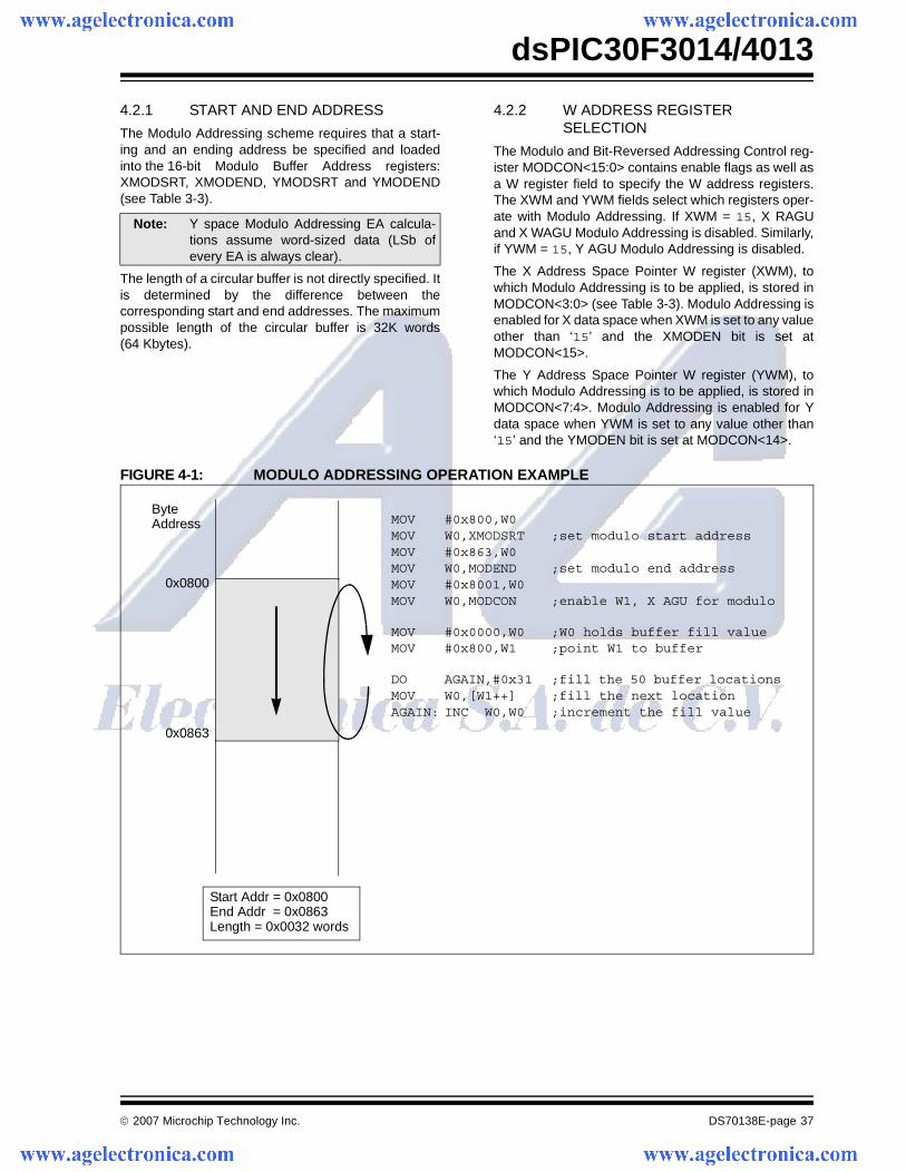
© 2007 Microchip Technology Inc. DS70138E-page 37
dsPIC30F3014/4013
4.2.1 START AND END ADDRESS
The Modulo Addressing scheme requires that a start-ing and an ending address be specified and loadedinto the 16-bit Modulo Buffer Address registers:XMODSRT, XMODEND, YMODSRT and YMODEND(see Table 3-3).
The length of a circular buffer is not directly specified. Itis determined by the difference between thecorresponding start and end addresses. The maximumpossible length of the circular buffer is 32K words(64 Kbytes).
4.2.2 W ADDRESS REGISTER SELECTION
The Modulo and Bit-Reversed Addressing Control reg-ister MODCON<15:0> contains enable flags as well asa W register field to specify the W address registers.The XWM and YWM fields select which registers oper-ate with Modulo Addressing. If XWM = 15, X RAGUand X WAGU Modulo Addressing is disabled. Similarly,if YWM = 15, Y AGU Modulo Addressing is disabled.
The X Address Space Pointer W register (XWM), towhich Modulo Addressing is to be applied, is stored inMODCON<3:0> (see Table 3-3). Modulo Addressing isenabled for X data space when XWM is set to any valueother than ‘15’ and the XMODEN bit is set atMODCON<15>.
The Y Address Space Pointer W register (YWM), towhich Modulo Addressing is to be applied, is stored inMODCON<7:4>. Modulo Addressing is enabled for Ydata space when YWM is set to any value other than‘15’ and the YMODEN bit is set at MODCON<14>.
FIGURE 4-1: MODULO ADDRESSING OPERATION EXAMPLE
Note: Y space Modulo Addressing EA calcula-tions assume word-sized data (LSb ofevery EA is always clear).
0x0800
0x0863
Start Addr = 0x0800End Addr = 0x0863Length = 0x0032 words
ByteAddress MOV #0x800,W0
MOV W0,XMODSRT ;set modulo start addressMOV #0x863,W0MOV W0,MODEND ;set modulo end addressMOV #0x8001,W0MOV W0,MODCON ;enable W1, X AGU for modulo
MOV #0x0000,W0 ;W0 holds buffer fill valueMOV #0x800,W1 ;point W1 to buffer
DO AGAIN,#0x31 ;fill the 50 buffer locationsMOV W0,[W1++] ;fill the next locationAGAIN: INC W0,W0 ;increment the fill value
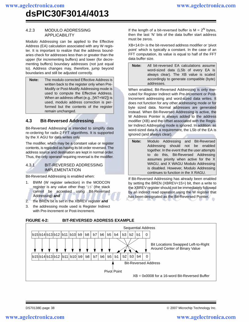
dsPIC30F3014/4013
DS70138E-page 38 © 2007 Microchip Technology Inc.
4.2.3 MODULO ADDRESSING APPLICABILITY
Modulo Addressing can be applied to the EffectiveAddress (EA) calculation associated with any W regis-ter. It is important to realize that the address bound-aries check for addresses less than or greater than theupper (for incrementing buffers) and lower (for decre-menting buffers) boundary addresses (not just equalto). Address changes may, therefore, jump beyondboundaries and still be adjusted correctly.
4.3 Bit-Reversed Addressing
Bit-Reversed Addressing is intended to simplify datare-ordering for radix-2 FFT algorithms. It is supportedby the X AGU for data writes only.
The modifier, which may be a constant value or registercontents, is regarded as having its bit order reversed. Theaddress source and destination are kept in normal order.Thus, the only operand requiring reversal is the modifier.
4.3.1 BIT-REVERSED ADDRESSING IMPLEMENTATION
Bit-Reversed Addressing is enabled when:
1. BWM (W register selection) in the MODCONregister is any value other than ‘15’ (the stackcannot be accessed using Bit-ReversedAddressing) and
2. the BREN bit is set in the XBREV register and3. the addressing mode used is Register Indirect
with Pre-Increment or Post-Increment.
If the length of a bit-reversed buffer is M = 2N bytes,then the last ‘N’ bits of the data buffer start addressmust be zeros.
XB<14:0> is the bit-reversed address modifier or ‘pivotpoint’ which is typically a constant. In the case of anFFT computation, its value is equal to half of the FFTdata buffer size.
When enabled, Bit-Reversed Addressing is only exe-cuted for Register Indirect with Pre-Increment or Post-Increment addressing and word-sized data writes. Itdoes not function for any other addressing mode or forbyte sized data. Normal addresses are generatedinstead. When Bit-Reversed Addressing is active, theW Address Pointer is always added to the addressmodifier (XB) and the offset associated with the Regis-ter Indirect Addressing mode is ignored. In addition, asword-sized data is a requirement, the LSb of the EA isignored (and always clear).
If Bit-Reversed Addressing has already been enabledby setting the BREN (XBREV<15>) bit, then a write tothe XBREV register should not be immediately followedby an indirect read operation using the W register thathas been designated as the Bit-Reversed Pointer.
FIGURE 4-2: BIT-REVERSED ADDRESS EXAMPLE
Note: The modulo corrected Effective Address iswritten back to the register only when Pre-Modify or Post-Modify Addressing mode isused to compute the Effective Address.When an address offset (e.g., [W7+W2]) isused, modulo address correction is per-formed but the contents of the registerremain unchanged.
Note: All bit-reversed EA calculations assumeword-sized data (LSb of every EA isalways clear). The XB value is scaledaccordingly to generate compatible (byte)addresses.
Note: Modulo Addressing and Bit-ReversedAddressing should not be enabledtogether. In the event that the user attemptsto do this, Bit-Reversed Addressingassumes priority when active for the XWAGU, and X WAGU Modulo Addressingis disabled. However, Modulo Addressingcontinues to function in the X RAGU.
b3 b2 b1 0
b2 b3 b4 0
Bit Locations Swapped Left-to-RightAround Center of Binary Value
Bit-Reversed Address
XB = 0x0008 for a 16-word Bit-Reversed Buffer
b7 b6 b5 b1
b7 b6 b5 b4b11 b10 b9 b8
b11 b10 b9 b8
b15 b14 b13 b12
b15 b14 b13 b12
Sequential Address
Pivot Point
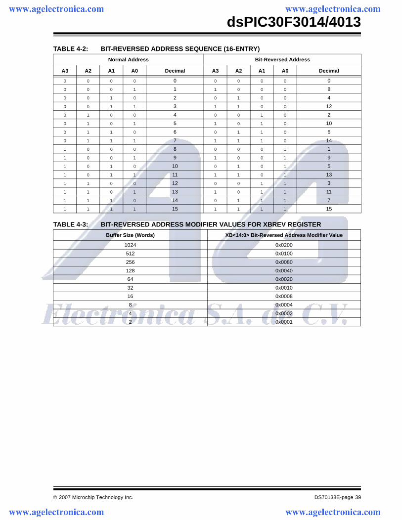
© 2007 Microchip Technology Inc. DS70138E-page 39
dsPIC30F3014/4013
TABLE 4-2: BIT-REVERSED ADDRESS SEQUENCE (16-ENTRY)
TABLE 4-3: BIT-REVERSED ADDRESS MODIFIER VALUES FOR XBREV REGISTER
Normal Address Bit-Reversed Address
A3 A2 A1 A0 Decimal A3 A2 A1 A0 Decimal
0 0 0 0 0 0 0 0 0 0
0 0 0 1 1 1 0 0 0 8
0 0 1 0 2 0 1 0 0 4
0 0 1 1 3 1 1 0 0 12
0 1 0 0 4 0 0 1 0 2
0 1 0 1 5 1 0 1 0 10
0 1 1 0 6 0 1 1 0 6
0 1 1 1 7 1 1 1 0 14
1 0 0 0 8 0 0 0 1 1
1 0 0 1 9 1 0 0 1 9
1 0 1 0 10 0 1 0 1 5
1 0 1 1 11 1 1 0 1 13
1 1 0 0 12 0 0 1 1 3
1 1 0 1 13 1 0 1 1 11
1 1 1 0 14 0 1 1 1 7
1 1 1 1 15 1 1 1 1 15
Buffer Size (Words) XB<14:0> Bit-Reversed Address Modifier Value
1024 0x0200
512 0x0100
256 0x0080
128 0x0040
64 0x0020
32 0x0010
16 0x0008
8 0x0004
4 0x0002
2 0x0001

dsPIC30F3014/4013
DS70138E-page 40 © 2007 Microchip Technology Inc.
NOTES:
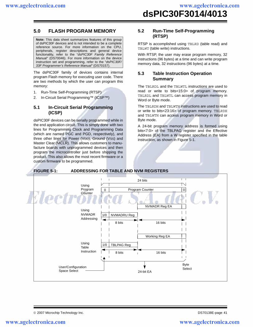
© 2007 Microchip Technology Inc. DS70138E-page 41
dsPIC30F3014/4013
5.0 FLASH PROGRAM MEMORY
The dsPIC30F family of devices contains internalprogram Flash memory for executing user code. Thereare two methods by which the user can program thismemory:
1. Run-Time Self-Programming (RTSP)2. In-Circuit Serial Programming™ (ICSP™)
5.1 In-Circuit Serial Programming (ICSP)
dsPIC30F devices can be serially programmed while inthe end application circuit. This is simply done with twolines for Programming Clock and Programming Data(which are named PGC and PGD, respectively), andthree other lines for Power (VDD), Ground (VSS) andMaster Clear (MCLR). This allows customers to manu-facture boards with unprogrammed devices and thenprogram the microcontroller just before shipping theproduct. This also allows the most recent firmware or acustom firmware to be programmed.
5.2 Run-Time Self-Programming (RTSP)
RTSP is accomplished using TBLRD (table read) andTBLWT (table write) instructions.
With RTSP, the user may erase program memory, 32instructions (96 bytes) at a time and can write programmemory data, 32 instructions (96 bytes) at a time.
5.3 Table Instruction Operation Summary
The TBLRDL and the TBLWTL instructions are used toread or write to bits<15:0> of program memory.TBLRDL and TBLWTL can access program memory inWord or Byte mode.
The TBLRDH and TBLWTH instructions are used to reador write to bits<23:16> of program memory. TBLRDHand TBLWTH can access program memory in Word orByte mode.
A 24-bit program memory address is formed usingbits<7:0> of the TBLPAG register and the EffectiveAddress (EA) from a W register specified in the tableinstruction, as shown in Figure 5-1.
FIGURE 5-1: ADDRESSING FOR TABLE AND NVM REGISTERS
Note: This data sheet summarizes features of this groupof dsPIC30F devices and is not intended to be a completereference source. For more information on the CPU,peripherals, register descriptions and general devicefunctionality, refer to the “dsPIC30F Family ReferenceManual” (DS70046). For more information on the deviceinstruction set and programming, refer to the “dsPIC30F/33F Programmer’s Reference Manual” (DS70157).
0Program Counter
24 bits
NVMADRU Reg
8 bits 16 bits
Program
Using
TBLPAG Reg
8 bits
Working Reg EA
16 bits
Using
Byte
24-bit EA
1/0
0
1/0
Select
TableInstruction
NVMADRAddressing
Counter
Using
NVMADR Reg EA
User/ConfigurationSpace Select
dsPIC30F3014/4013
DS70138E-page 42 © 2007 Microchip Technology Inc.
5.4 RTSP Operation
The dsPIC30F Flash program memory is organizedinto rows and panels. Each row consists of 32 instruc-tions or 96 bytes. Each panel consists of 128 rows or4K x 24 instructions. RTSP allows the user to erase onerow (32 instructions) at a time and to program fourinstructions at one time. RTSP may be used to programmultiple program memory panels, but the Table Pointermust be changed at each panel boundary.
Each panel of program memory contains write latchesthat hold 32 instructions of programming data. Prior tothe actual programming operation, the write data mustbe loaded into the panel write latches. The data to beprogrammed into the panel is loaded in sequentialorder into the write latches; instruction 0, instruction 1,etc. The instruction words loaded must always be froma 32 address boundary.
The basic sequence for RTSP programming is to set upa Table Pointer, then do a series of TBLWT instructionsto load the write latches. Programming is performed bysetting the special bits in the NVMCON register. 32TBLWTL and four TBLWTH instructions are required toload the 32 instructions. If multiple panel programmingis required, the Table Pointer needs to be changed andthe next set of multiple write latches written.
All of the table write operations are single-word writes(2 instruction cycles), because only the table latchesare written. A programming cycle is required forprogramming each row.
The Flash Program Memory is readable, writable anderasable during normal operation over the entire VDD
range.
5.5 Control Registers
The four SFRs used to read and write the programFlash memory are:
• NVMCON• NVMADR
• NVMADRU• NVMKEY
5.5.1 NVMCON REGISTER
The NVMCON register controls which blocks are to beerased, which memory type is to be programmed, andstart of the programming cycle.
5.5.2 NVMADR REGISTER
The NVMADR register is used to hold the lower twobytes of the Effective Address. The NVMADR registercaptures the EA<15:0> of the last table instruction thathas been executed and selects the row to write.
5.5.3 NVMADRU REGISTER
The NVMADRU register is used to hold the upper byteof the Effective Address. The NVMADRU register cap-tures the EA<23:16> of the last table instruction thathas been executed.
5.5.4 NVMKEY REGISTER
NVMKEY is a write-only register that is used for writeprotection. To start a programming or an erasesequence, the user must consecutively write 0x55 and0xAA to the NVMKEY register. Refer to Section 5.6“Programming Operations” for further details.
Note: The user can also directly write to theNVMADR and NVMADRU registers tospecify a program memory address forerasing or programming.
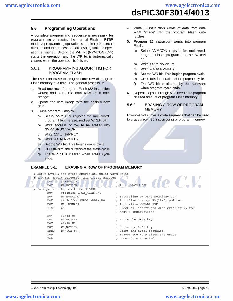
© 2007 Microchip Technology Inc. DS70138E-page 43
dsPIC30F3014/4013
5.6 Programming Operations
A complete programming sequence is necessary forprogramming or erasing the internal Flash in RTSPmode. A programming operation is nominally 2 msec induration and the processor stalls (waits) until the oper-ation is finished. Setting the WR bit (NVMCON<15>)starts the operation and the WR bit is automaticallycleared when the operation is finished.
5.6.1 PROGRAMMING ALGORITHM FOR PROGRAM FLASH
The user can erase or program one row of programFlash memory at a time. The general process is:
1. Read one row of program Flash (32 instructionwords) and store into data RAM as a data“image”.
2. Update the data image with the desired newdata.
3. Erase program Flash row.a) Setup NVMCON register for multi-word,
program Flash, erase, and set WREN bit.b) Write address of row to be erased into
NVMADRU/NVMDR.c) Write ‘55’ to NVMKEY.d) Write ‘AA’ to NVMKEY.
e) Set the WR bit. This begins erase cycle.f) CPU stalls for the duration of the erase cycle.g) The WR bit is cleared when erase cycle
ends.
4. Write 32 instruction words of data from dataRAM “image” into the program Flash writelatches.
5. Program 32 instruction words into programFlash.
a) Setup NVMCON register for multi-word,program Flash, program, and set WRENbit.
b) Write ‘55’ to NVMKEY.
c) Write ‘AA’ to NVMKEY.d) Set the WR bit. This begins program cycle.e) CPU stalls for duration of the program cycle.
f) The WR bit is cleared by the hardwarewhen program cycle ends.
6. Repeat steps 1 through 5 as needed to programdesired amount of program Flash memory.
5.6.2 ERASING A ROW OF PROGRAM MEMORY
Example 5-1 shows a code sequence that can be usedto erase a row (32 instructions) of program memory.
EXAMPLE 5-1: ERASING A ROW OF PROGRAM MEMORY
; Setup NVMCON for erase operation, multi word write; program memory selected, and writes enabled
MOV #0x4041,W0 ;MOV W0,NVMCON ; Init NVMCON SFR
; Init pointer to row to be ERASEDMOV #tblpage(PROG_ADDR),W0 ; MOV W0,NVMADRU ; Initialize PM Page Boundary SFRMOV #tbloffset(PROG_ADDR),W0 ; Intialize in-page EA[15:0] pointerMOV W0, NVMADR ; Initialize NVMADR SFRDISI #5 ; Block all interrupts with priority <7 for
; next 5 instructionsMOV #0x55,W0MOV W0,NVMKEY ; Write the 0x55 key MOV #0xAA,W1 ;MOV W1,NVMKEY ; Write the 0xAA keyBSET NVMCON,#WR ; Start the erase sequence NOP ; Insert two NOPs after the eraseNOP ; command is asserted
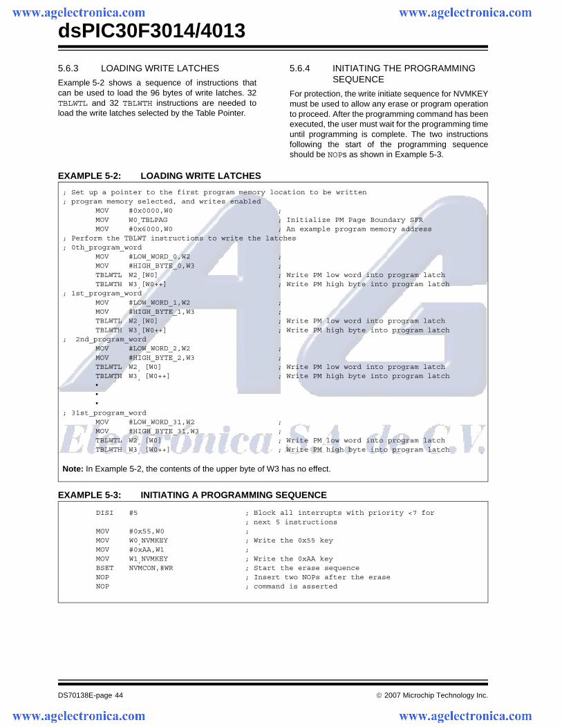
dsPIC30F3014/4013
DS70138E-page 44 © 2007 Microchip Technology Inc.
5.6.3 LOADING WRITE LATCHES
Example 5-2 shows a sequence of instructions thatcan be used to load the 96 bytes of write latches. 32TBLWTL and 32 TBLWTH instructions are needed toload the write latches selected by the Table Pointer.
5.6.4 INITIATING THE PROGRAMMING SEQUENCE
For protection, the write initiate sequence for NVMKEYmust be used to allow any erase or program operationto proceed. After the programming command has beenexecuted, the user must wait for the programming timeuntil programming is complete. The two instructionsfollowing the start of the programming sequenceshould be NOPs as shown in Example 5-3.
EXAMPLE 5-2: LOADING WRITE LATCHES
EXAMPLE 5-3: INITIATING A PROGRAMMING SEQUENCE
; Set up a pointer to the first program memory location to be written; program memory selected, and writes enabled
MOV #0x0000,W0 ; MOV W0,TBLPAG ; Initialize PM Page Boundary SFRMOV #0x6000,W0 ; An example program memory address
; Perform the TBLWT instructions to write the latches; 0th_program_word
MOV #LOW_WORD_0,W2 ; MOV #HIGH_BYTE_0,W3 ; TBLWTL W2,[W0] ; Write PM low word into program latchTBLWTH W3,[W0++] ; Write PM high byte into program latch
; 1st_program_wordMOV #LOW_WORD_1,W2 ; MOV #HIGH_BYTE_1,W3 ; TBLWTL W2,[W0] ; Write PM low word into program latchTBLWTH W3,[W0++] ; Write PM high byte into program latch
; 2nd_program_wordMOV #LOW_WORD_2,W2 ; MOV #HIGH_BYTE_2,W3 ; TBLWTL W2, [W0] ; Write PM low word into program latchTBLWTH W3, [W0++] ; Write PM high byte into program latch•••
; 31st_program_wordMOV #LOW_WORD_31,W2 ; MOV #HIGH_BYTE_31,W3 ; TBLWTL W2, [W0] ; Write PM low word into program latchTBLWTH W3, [W0++] ; Write PM high byte into program latch
Note: In Example 5-2, the contents of the upper byte of W3 has no effect.
DISI #5 ; Block all interrupts with priority <7 for; next 5 instructions
MOV #0x55,W0 ; MOV W0,NVMKEY ; Write the 0x55 keyMOV #0xAA,W1 ;MOV W1,NVMKEY ; Write the 0xAA keyBSET NVMCON,#WR ; Start the erase sequence NOP ; Insert two NOPs after the eraseNOP ; command is asserted
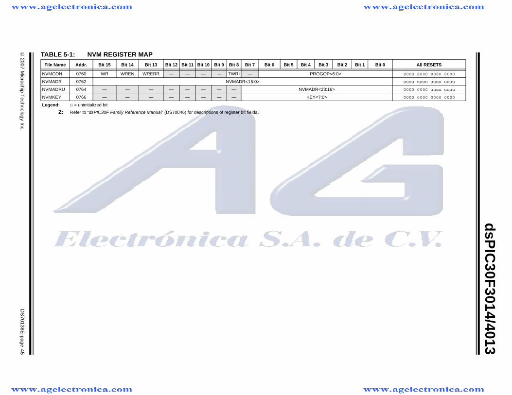
© 2007 M
icrochip Technology Inc.
DS
70138E-page 45
dsP
IC30F
3014/4013
TABLE 5-1: NVM REGISTER MAP
File Name Addr. Bit 15 Bit 14 Bit 13 Bit 12 Bit 11 Bit 10 Bit 9 Bit 8 Bit 7 Bit 6 Bit 5 Bit 4 Bit 3 Bit 2 Bit 1 Bit 0 All RESETS
NVMCON 0760 WR WREN WRERR — — — — TWRI — PROGOP<6:0> 0000 0000 0000 0000
NVMADR 0762 NVMADR<15:0> uuuu uuuu uuuu uuuu
NVMADRU 0764 — — — — — — — — NVMADR<23:16> 0000 0000 uuuu uuuu
NVMKEY 0766 — — — — — — — — KEY<7:0> 0000 0000 0000 0000
Legend: u = uninitialized bit
2: Refer to “dsPIC30F Family Reference Manual” (DS70046) for descriptions of register bit fields.

dsPIC30F3014/4013
DS70138E-page 46 © 2007 Microchip Technology Inc.
NOTES:
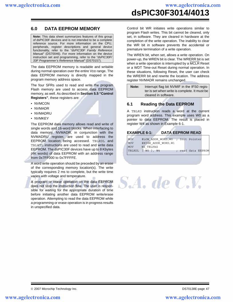
© 2007 Microchip Technology Inc. DS70138E-page 47
dsPIC30F3014/4013
6.0 DATA EEPROM MEMORY
The data EEPROM memory is readable and writableduring normal operation over the entire VDD range. Thedata EEPROM memory is directly mapped in theprogram memory address space.
The four SFRs used to read and write the programFlash memory are used to access data EEPROMmemory, as well. As described in Section 5.5 “ControlRegisters”, these registers are:
• NVMCON• NVMADR• NVMADRU
• NVMKEY
The EEPROM data memory allows read and write ofsingle words and 16-word blocks. When interfacing todata memory, NVMADR, in conjunction with theNVMADRU register, are used to address theEEPROM location being accessed. TBLRDL andTBLWTL instructions are used to read and write dataEEPROM. The dsPIC30F devices have up to 8 Kbytes(4K words) of data EEPROM with an address rangefrom 0x7FF000 to 0x7FFFFE.
A word write operation should be preceded by an eraseof the corresponding memory location(s). The writetypically requires 2 ms to complete, but the write timevaries with voltage and temperature.
A program or erase operation on the data EEPROMdoes not stop the instruction flow. The user is respon-sible for waiting for the appropriate duration of timebefore initiating another data EEPROM write/eraseoperation. Attempting to read the data EEPROM whilea programming or erase operation is in progress resultsin unspecified data.
Control bit WR initiates write operations similar toprogram Flash writes. This bit cannot be cleared, onlyset, in software. They are cleared in hardware at thecompletion of the write operation. The inability to clearthe WR bit in software prevents the accidental orpremature termination of a write operation.
The WREN bit, when set, allows a write operation. Onpower-up, the WREN bit is clear. The WRERR bit is setwhen a write operation is interrupted by a MCLR Resetor a WDT Time-out Reset during normal operation. Inthese situations, following Reset, the user can checkthe WRERR bit and rewrite the location. The addressregister NVMADR remains unchanged.
6.1 Reading the Data EEPROM
A TBLRD instruction reads a word at the currentprogram word address. This example uses W0 as apointer to data EEPROM. The result is placed inregister W4 as shown in Example 6-1.
EXAMPLE 6-1: DATA EEPROM READ
Note: This data sheet summarizes features of this groupof dsPIC30F devices and is not intended to be a completereference source. For more information on the CPU,peripherals, register descriptions and general devicefunctionality, refer to the “dsPIC30F Family ReferenceManual” (DS70046). For more information on the deviceinstruction set and programming, refer to the “dsPIC30F/33F Programmer’s Reference Manual” (DS70157).
Note: Interrupt flag bit NVMIF in the IFS0 regis-ter is set when write is complete. It must becleared in software.
MOV #LOW_ADDR_WORD,W0 ; Init PointerMOV #HIGH_ADDR_WORD,W1MOV W1,TBLPAG TBLRDL [ W0 ], W4 ; read data EEPROM
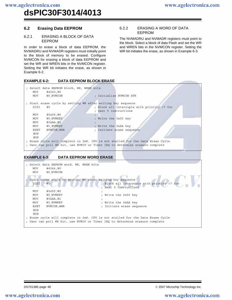
dsPIC30F3014/4013
DS70138E-page 48 © 2007 Microchip Technology Inc.
6.2 Erasing Data EEPROM
6.2.1 ERASING A BLOCK OF DATA EEPROM
In order to erase a block of data EEPROM, theNVMADRU and NVMADR registers must initially pointto the block of memory to be erased. ConfigureNVMCON for erasing a block of data EEPROM andset the WR and WREN bits in the NVMCON register.Setting the WR bit initiates the erase, as shown inExample 6-2.
6.2.2 ERASING A WORD OF DATA EEPROM
The NVMADRU and NVMADR registers must point tothe block. Select a block of data Flash and set the WRand WREN bits in the NVMCON register. Setting theWR bit initiates the erase, as shown in Example 6-3.
EXAMPLE 6-2: DATA EEPROM BLOCK ERASE
EXAMPLE 6-3: DATA EEPROM WORD ERASE
; Select data EEPROM block, WR, WREN bitsMOV #4045,W0MOV W0,NVMCON ; Initialize NVMCON SFR
; Start erase cycle by setting WR after writing key sequence
DISI #5 ; Block all interrupts with priority <7 for; next 5 instructions
MOV #0x55,W0 ; MOV W0,NVMKEY ; Write the 0x55 keyMOV #0xAA,W1 ;MOV W1,NVMKEY ; Write the 0xAA keyBSET NVMCON,#WR ; Initiate erase sequence
NOP NOP ; Erase cycle will complete in 2mS. CPU is not stalled for the Data Erase Cycle; User can poll WR bit, use NVMIF or Timer IRQ to determine erasure complete
; Select data EEPROM word, WR, WREN bitsMOV #4044,W0MOV W0,NVMCON
; Start erase cycle by setting WR after writing key sequence
DISI #5 ; Block all interrupts with priority <7 for; next 5 instructions
MOV #0x55,W0 ; MOV W0,NVMKEY ; Write the 0x55 key
MOV #0xAA,W1 ;MOV W1,NVMKEY ; Write the 0xAA key
BSET NVMCON,#WR ; Initiate erase sequence NOP NOP ; Erase cycle will complete in 2mS. CPU is not stalled for the Data Erase Cycle; User can poll WR bit, use NVMIF or Timer IRQ to determine erasure complete
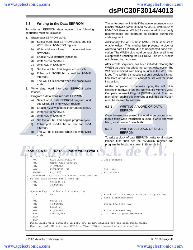
© 2007 Microchip Technology Inc. DS70138E-page 49
dsPIC30F3014/4013
6.3 Writing to the Data EEPROM
To write an EEPROM data location, the followingsequence must be followed:
1. Erase data EEPROM word.a) Select word, data EEPROM erase, and set
WREN bit in NVMCON register.b) Write address of word to be erased into
NVMADR.c) Enable NVM interrupt (optional).
d) Write ‘55’ to NVMKEY.e) Write ‘AA’ to NVMKEY.f) Set the WR bit. This begins erase cycle.
g) Either poll NVMIF bit or wait for NVMIFinterrupt.
h) The WR bit is cleared when the erase cycleends.
2. Write data word into data EEPROM writelatches.
3. Program 1 data word into data EEPROM.a) Select word, data EEPROM program, and
set WREN bit in NVMCON register.b) Enable NVM write done interrupt (optional).c) Write ‘55’ to NVMKEY.
d) Write ‘AA’ to NVMKEY.e) Set the WR bit. This begins program cycle.f) Either poll NVMIF bit or wait for NVM
interrupt.g) The WR bit is cleared when the write cycle
ends.
The write does not initiate if the above sequence is notexactly followed (write 0x55 to NVMKEY, write 0xAA toNVMCON, then set WR bit) for each word. It is stronglyrecommended that interrupts be disabled during thiscode segment.
Additionally, the WREN bit in NVMCON must be set toenable writes. This mechanism prevents accidentalwrites to data EEPROM due to unexpected code exe-cution. The WREN bit should be kept clear at all timesexcept when updating the EEPROM. The WREN bit isnot cleared by hardware.
After a write sequence has been initiated, clearing theWREN bit does not affect the current write cycle. TheWR bit is inhibited from being set unless the WREN bitis set. The WREN bit must be set on a previous instruc-tion. Both WR and WREN cannot be set with the sameinstruction.
At the completion of the write cycle, the WR bit iscleared in hardware and the Nonvolatile Memory WriteComplete Interrupt Flag bit (NVMIF) is set. The usermay either enable this interrupt or poll this bit. NVMIFmust be cleared by software.
6.3.1 WRITING A WORD OF DATA EEPROM
Once the user has erased the word to be programmed,then a table write instruction is used to write one writelatch, as shown in Example 6-4.
6.3.2 WRITING A BLOCK OF DATA EEPROM
To write a block of data EEPROM, write to all sixteenlatches first, then set the NVMCON register andprogram the block, as shown in Example 6-5.
EXAMPLE 6-4: DATA EEPROM WORD WRITE
; Point to data memoryMOV #LOW_ADDR_WORD,W0 ; Init pointerMOV #HIGH_ADDR_WORD,W1MOV W1,TBLPAGMOV #LOW(WORD),W2 ; Get dataTBLWTL W2,[ W0] ; Write data
; The NVMADR captures last table access address; Select data EEPROM for 1 word op
MOV #0x4004,W0MOV W0,NVMCON
; Operate key to allow write operation
DISI #5 ; Block all interrupts with priority <7 for; next 5 instructions
MOV #0x55,W0MOV W0,NVMKEY ; Write the 0x55 keyMOV #0xAA,W1MOV W1,NVMKEY ; Write the 0xAA keyBSET NVMCON,#WR ; Initiate program sequence
NOP NOP ; Write cycle will complete in 2mS. CPU is not stalled for the Data Write Cycle; User can poll WR bit, use NVMIF or Timer IRQ to determine write complete
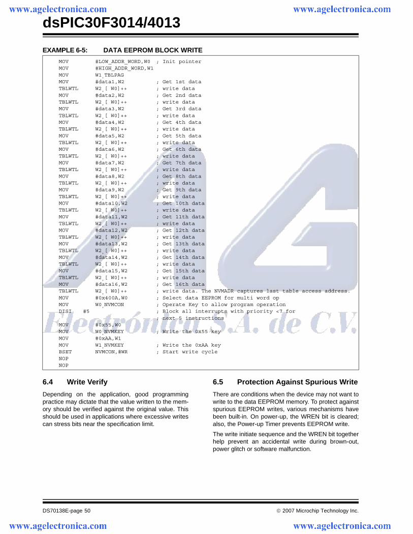
dsPIC30F3014/4013
DS70138E-page 50 © 2007 Microchip Technology Inc.
EXAMPLE 6-5: DATA EEPROM BLOCK WRITE
6.4 Write Verify
Depending on the application, good programmingpractice may dictate that the value written to the mem-ory should be verified against the original value. Thisshould be used in applications where excessive writescan stress bits near the specification limit.
6.5 Protection Against Spurious Write
There are conditions when the device may not want towrite to the data EEPROM memory. To protect againstspurious EEPROM writes, various mechanisms havebeen built-in. On power-up, the WREN bit is cleared;also, the Power-up Timer prevents EEPROM write.
The write initiate sequence and the WREN bit togetherhelp prevent an accidental write during brown-out,power glitch or software malfunction.
MOV #LOW_ADDR_WORD,W0 ; Init pointer MOV #HIGH_ADDR_WORD,W1 MOV W1,TBLPAG MOV #data1,W2 ; Get 1st data TBLWTL W2,[ W0]++ ; write data MOV #data2,W2 ; Get 2nd data TBLWTL W2,[ W0]++ ; write data MOV #data3,W2 ; Get 3rd data TBLWTL W2,[ W0]++ ; write data MOV #data4,W2 ; Get 4th data TBLWTL W2,[ W0]++ ; write data MOV #data5,W2 ; Get 5th data TBLWTL W2,[ W0]++ ; write data MOV #data6,W2 ; Get 6th data TBLWTL W2,[ W0]++ ; write data MOV #data7,W2 ; Get 7th data TBLWTL W2,[ W0]++ ; write data MOV #data8,W2 ; Get 8th data TBLWTL W2,[ W0]++ ; write data MOV #data9,W2 ; Get 9th data TBLWTL W2,[ W0]++ ; write data MOV #data10,W2 ; Get 10th data TBLWTL W2,[ W0]++ ; write data MOV #data11,W2 ; Get 11th data TBLWTL W2,[ W0]++ ; write data MOV #data12,W2 ; Get 12th data TBLWTL W2,[ W0]++ ; write data MOV #data13,W2 ; Get 13th data TBLWTL W2,[ W0]++ ; write data MOV #data14,W2 ; Get 14th data TBLWTL W2,[ W0]++ ; write data MOV #data15,W2 ; Get 15th data TBLWTL W2,[ W0]++ ; write data MOV #data16,W2 ; Get 16th data TBLWTL W2,[ W0]++ ; write data. The NVMADR captures last table access address. MOV #0x400A,W0 ; Select data EEPROM for multi word op MOV W0,NVMCON ; Operate Key to allow program operation
DISI #5 ; Block all interrupts with priority <7 for; next 5 instructions
MOV #0x55,W0 MOV W0,NVMKEY ; Write the 0x55 key MOV #0xAA,W1 MOV W1,NVMKEY ; Write the 0xAA key BSET NVMCON,#WR ; Start write cycle NOP NOP
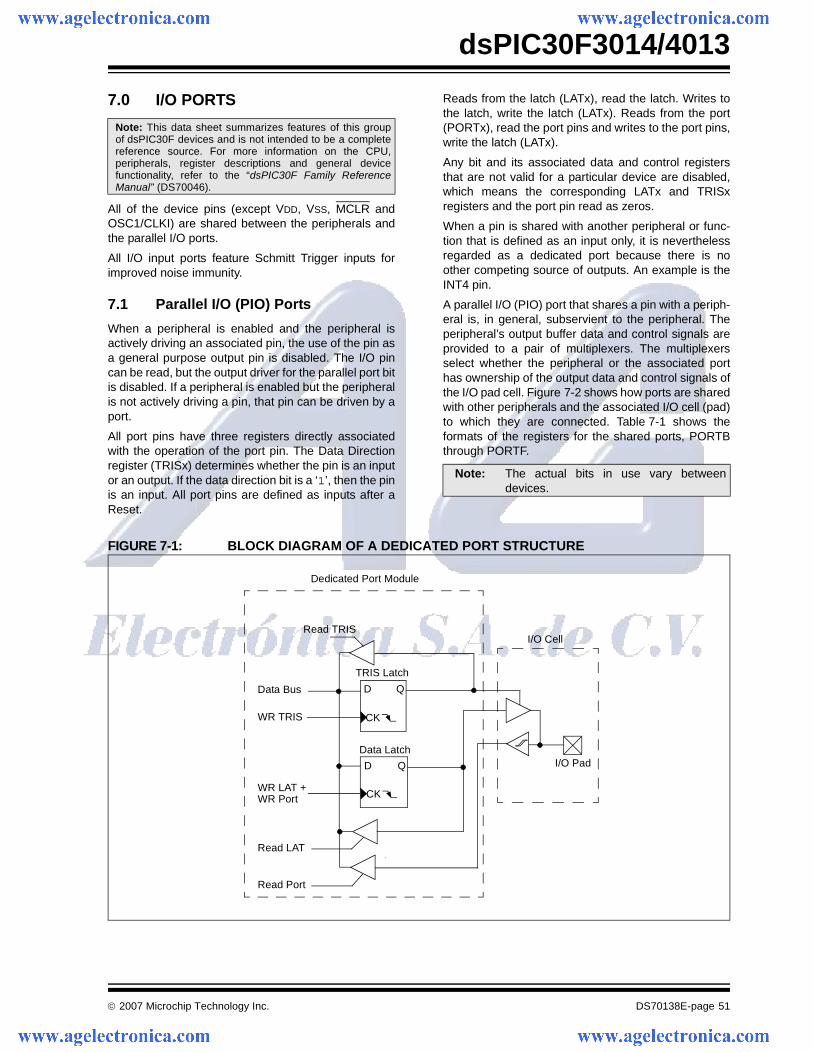
© 2007 Microchip Technology Inc. DS70138E-page 51
dsPIC30F3014/4013
7.0 I/O PORTS
All of the device pins (except VDD, VSS, MCLR andOSC1/CLKI) are shared between the peripherals andthe parallel I/O ports.
All I/O input ports feature Schmitt Trigger inputs forimproved noise immunity.
7.1 Parallel I/O (PIO) Ports
When a peripheral is enabled and the peripheral isactively driving an associated pin, the use of the pin asa general purpose output pin is disabled. The I/O pincan be read, but the output driver for the parallel port bitis disabled. If a peripheral is enabled but the peripheralis not actively driving a pin, that pin can be driven by aport.
All port pins have three registers directly associatedwith the operation of the port pin. The Data Directionregister (TRISx) determines whether the pin is an inputor an output. If the data direction bit is a ‘1’, then the pinis an input. All port pins are defined as inputs after aReset.
Reads from the latch (LATx), read the latch. Writes tothe latch, write the latch (LATx). Reads from the port(PORTx), read the port pins and writes to the port pins,write the latch (LATx).
Any bit and its associated data and control registersthat are not valid for a particular device are disabled,which means the corresponding LATx and TRISxregisters and the port pin read as zeros.
When a pin is shared with another peripheral or func-tion that is defined as an input only, it is neverthelessregarded as a dedicated port because there is noother competing source of outputs. An example is theINT4 pin.
A parallel I/O (PIO) port that shares a pin with a periph-eral is, in general, subservient to the peripheral. Theperipheral’s output buffer data and control signals areprovided to a pair of multiplexers. The multiplexersselect whether the peripheral or the associated porthas ownership of the output data and control signals ofthe I/O pad cell. Figure 7-2 shows how ports are sharedwith other peripherals and the associated I/O cell (pad)to which they are connected. Table 7-1 shows theformats of the registers for the shared ports, PORTBthrough PORTF.
FIGURE 7-1: BLOCK DIAGRAM OF A DEDICATED PORT STRUCTURE
Note: This data sheet summarizes features of this groupof dsPIC30F devices and is not intended to be a completereference source. For more information on the CPU,peripherals, register descriptions and general devicefunctionality, refer to the “dsPIC30F Family ReferenceManual” (DS70046).
Note: The actual bits in use vary betweendevices.
QD
CK
WR LAT +
TRIS Latch
I/O Pad
WR Port
Data Bus
QD
CK
Data Latch
Read LAT
Read Port
Read TRIS
WR TRIS
I/O Cell
Dedicated Port Module
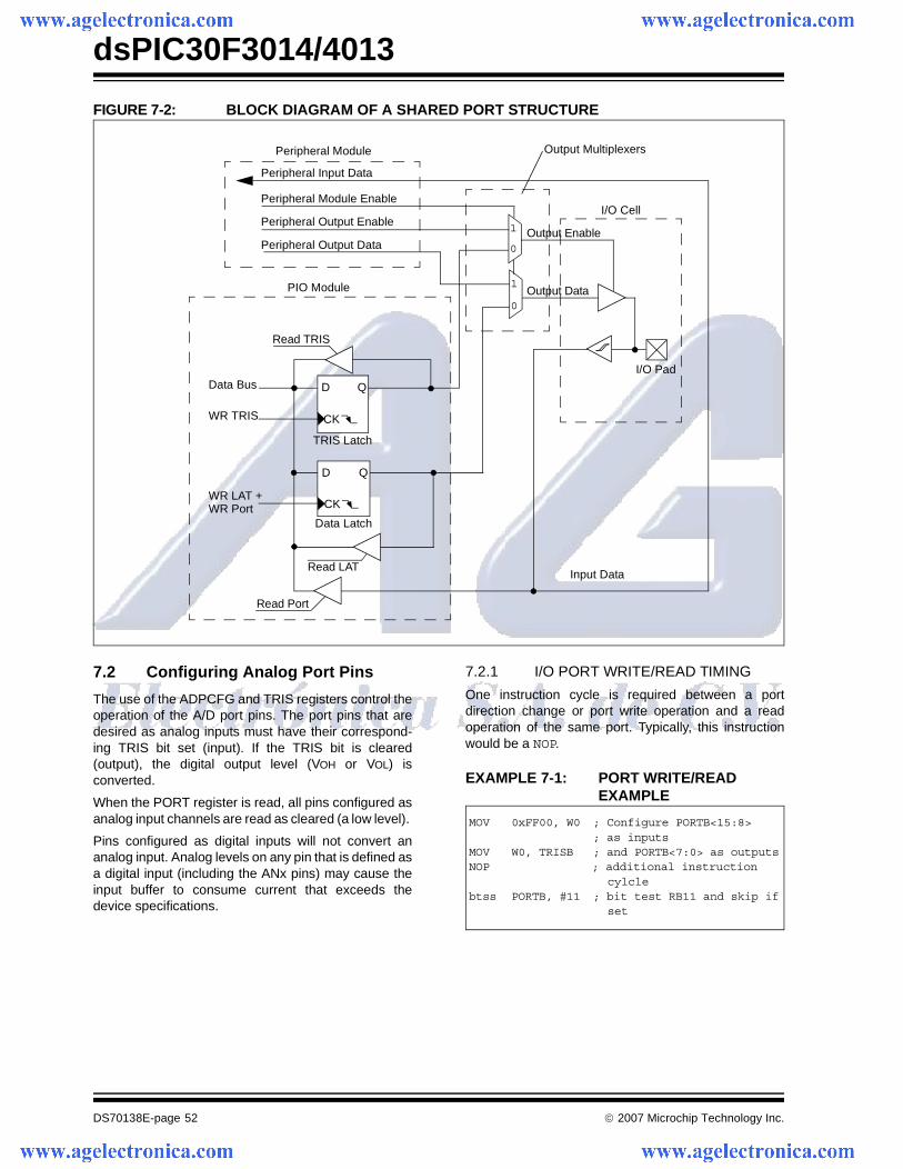
dsPIC30F3014/4013
DS70138E-page 52 © 2007 Microchip Technology Inc.
FIGURE 7-2: BLOCK DIAGRAM OF A SHARED PORT STRUCTURE
7.2 Configuring Analog Port Pins
The use of the ADPCFG and TRIS registers control theoperation of the A/D port pins. The port pins that aredesired as analog inputs must have their correspond-ing TRIS bit set (input). If the TRIS bit is cleared(output), the digital output level (VOH or VOL) isconverted.
When the PORT register is read, all pins configured asanalog input channels are read as cleared (a low level).
Pins configured as digital inputs will not convert ananalog input. Analog levels on any pin that is defined asa digital input (including the ANx pins) may cause theinput buffer to consume current that exceeds thedevice specifications.
7.2.1 I/O PORT WRITE/READ TIMING
One instruction cycle is required between a portdirection change or port write operation and a readoperation of the same port. Typically, this instructionwould be a NOP.
EXAMPLE 7-1: PORT WRITE/READ EXAMPLE
QD
CK
WR LAT +
TRIS Latch
I/O Pad
WR Port
Data Bus
QD
CK
Data Latch
Read LAT
Read Port
Read TRIS
1
0
1
0
WR TRIS
Peripheral Output DataOutput Enable
Peripheral Input Data
I/O Cell
Peripheral Module
Peripheral Output Enable
PIO Module
Output Multiplexers
Output Data
Input Data
Peripheral Module Enable
MOV 0xFF00, W0 ; Configure PORTB<15:8>; as inputs
MOV W0, TRISB ; and PORTB<7:0> as outputsNOP ; additional instruction
cylclebtss PORTB, #11 ; bit test RB11 and skip if
set
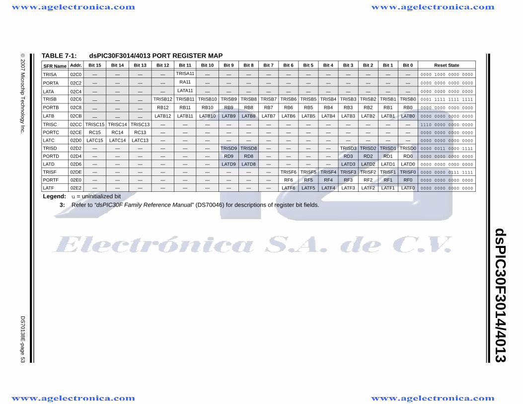
© 2007 M
icrochip Technology Inc.
DS
70138E-page 53
dsP
IC30F
3014/4013
TABLE 7-1: dsPIC30F3014/4013 PORT REGISTER MAPSFR Name Addr. Bit 15 Bit 14 Bit 13 Bit 12 Bit 11 Bit 10 Bit 9 Bit 8 Bit 7 Bit 6 Bit 5 Bit 4 Bit 3 Bit 2 Bit 1 Bit 0 Reset State
TRISA 02C0 — — — — TRISA11 — — — — — — — — — — — 0000 1000 0000 0000
PORTA 02C2 — — — — RA11 — — — — — — — — — — — 0000 0000 0000 0000
LATA 02C4 — — — — LATA11 — — — — — — — — — — — 0000 0000 0000 0000
TRISB 02C6 — — — TRISB12 TRISB11 TRISB10 TRISB9 TRISB8 TRISB7 TRISB6 TRISB5 TRISB4 TRISB3 TRISB2 TRISB1 TRISB0 0001 1111 1111 1111
PORTB 02C8 — — — RB12 RB11 RB10 RB9 RB8 RB7 RB6 RB5 RB4 RB3 RB2 RB1 RB0 0000 0000 0000 0000
LATB 02CB — — — LATB12 LATB11 LATB10 LATB9 LATB8 LATB7 LATB6 LATB5 LATB4 LATB3 LATB2 LATB1 LATB0 0000 0000 0000 0000
TRISC 02CC TRISC15 TRISC14 TRISC13 — — — — — — — — — — — — — 1110 0000 0000 0000
PORTC 02CE RC15 RC14 RC13 — — — — — — — — — — — — — 0000 0000 0000 0000
LATC 02D0 LATC15 LATC14 LATC13 — — — — — — — — — — — — — 0000 0000 0000 0000
TRISD 02D2 — — — — — — TRISD9 TRISD8 — — — — TRISD3 TRISD2 TRISD1 TRISD0 0000 0011 0000 1111
PORTD 02D4 — — — — — — RD9 RD8 — — — — RD3 RD2 RD1 RD0 0000 0000 0000 0000
LATD 02D6 — — — — — — LATD9 LATD8 — — — — LATD3 LATD2 LATD1 LATD0 0000 0000 0000 0000
TRISF 02DE — — — — — — — — — TRISF6 TRISF5 TRISF4 TRISF3 TRISF2 TRISF1 TRISF0 0000 0000 0111 1111
PORTF 02E0 — — — — — — — — — RF6 RF5 RF4 RF3 RF2 RF1 RF0 0000 0000 0000 0000
LATF 02E2 — — — — — — — — — LATF6 LATF5 LATF4 LATF3 LATF2 LATF1 LATF0 0000 0000 0000 0000
Legend: u = uninitialized bit3: Refer to “dsPIC30F Family Reference Manual” (DS70046) for descriptions of register bit fields.
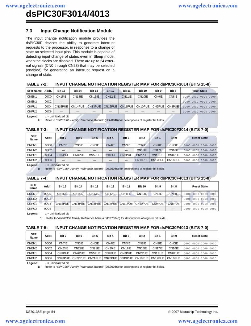
dsPIC30F3014/4013
DS70138E-page 54 © 2007 Microchip Technology Inc.
7.3 Input Change Notification Module
The input change notification module provides thedsPIC30F devices the ability to generate interruptrequests to the processor, in response to a change ofstate on selected input pins. This module is capable ofdetecting input change of states even in Sleep mode,when the clocks are disabled. There are up to 24 exter-nal signals (CN0 through CN23) that may be selected(enabled) for generating an interrupt request on achange of state.
TABLE 7-2: INPUT CHANGE NOTIFICATION REGISTER MAP FOR dsPIC30F3014 (BITS 15-8)
TABLE 7-3: INPUT CHANGE NOTIFICATION REGISTER MAP FOR dsPIC30F3014 (BITS 7-0)
TABLE 7-4: INPUT CHANGE NOTIFICATION REGISTER MAP FOR dsPIC30F4013 (BITS 15-8)
TABLE 7-5: INPUT CHANGE NOTIFICATION REGISTER MAP FOR dsPIC30F4013 (BITS 7-0)
SFR Name Addr. Bit 15 Bit 14 Bit 13 Bit 12 Bit 11 Bit 10 Bit 9 Bit 8 Reset State
CNEN1 00C0 CN15IE CN14IE CN13IE CN12IE CN11IE CN10IE CN9IE CN8IE 0000 0000 0000 0000
CNEN2 00C2 — — — — — — — — 0000 0000 0000 0000
CNPU1 00C4 CN15PUE CN14PUE CN13PUE CN12PUE CN11PUE CN10PUE CN9PUE CN8PUE 0000 0000 0000 0000
CNPU2 00C6 — — — — — — — — 0000 0000 0000 0000
Legend: u = uninitialized bit1: Refer to “dsPIC30F Family Reference Manual” (DS70046) for descriptions of register bit fields.
SFR Name Addr. Bit 7 Bit 6 Bit 5 Bit 4 Bit 3 Bit 2 Bit 1 Bit 0 Reset State
CNEN1 00C0 CN7IE CN6IE CN5IE CN4IE CN3IE CN2IE CN1IE CN0IE 0000 0000 0000 0000
CNEN2 00C2 — — — — — CN18IE CN17IE CN16IE 0000 0000 0000 0000
CNPU1 00C4 CN7PUE CN6PUE CN5PUE CN4PUE CN3PUE CN2PUE CN1PUE CN0PUE 0000 0000 0000 0000
CNPU2 00C6 — — — — — CN18PUE CN17PUE CN16PUE 0000 0000 0000 0000
Legend: u = uninitialized bit1: Refer to “dsPIC30F Family Reference Manual” (DS70046) for descriptions of register bit fields.
SFR Name Addr. Bit 15 Bit 14 Bit 13 Bit 12 Bit 11 Bit 10 Bit 9 Bit 8 Reset State
CNEN1 00C0 CN15IE CN14IE CN13IE CN12IE CN11IE CN10IE CN9IE CN8IE 0000 0000 0000 0000
CNEN2 00C2 — — — — — — — — 0000 0000 0000 0000
CNPU1 00C4 CN15PUE CN14PUE CN13PUE CN12PUE CN11PUE CN10PUE CN9PUE CN8PUE 0000 0000 0000 0000
CNPU2 00C6 — — — — — — — — 0000 0000 0000 0000
Legend: u = uninitialized bit
1: Refer to “dsPIC30F Family Reference Manual” (DS70046) for descriptions of register bit fields.
SFR Name Addr. Bit 7 Bit 6 Bit 5 Bit 4 Bit 3 Bit 2 Bit 1 Bit 0 Reset State
CNEN1 00C0 CN7IE CN6IE CN5IE CN4IE CN3IE CN2IE CN1IE CN0IE 0000 0000 0000 0000
CNEN2 00C2 CN23IE CN22IE CN21IE CN20IE CN19IE CN18IE CN17IE CN16IE 0000 0000 0000 0000
CNPU1 00C4 CN7PUE CN6PUE CN5PUE CN4PUE CN3PUE CN2PUE CN1PUE CN0PUE 0000 0000 0000 0000
CNPU2 00C6 CN23PUE CN22PUE CN21PUE CN20PUE CN19PUE CN18PUE CN17PUE CN16PUE 0000 0000 0000 0000
Legend: u = uninitialized bit1: Refer to “dsPIC30F Family Reference Manual” (DS70046) for descriptions of register bit fields.
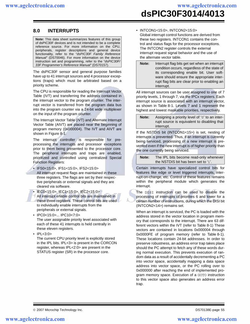
© 2007 Microchip Technology Inc. DS70138E-page 55
dsPIC30F3014/4013
8.0 INTERRUPTS
The dsPIC30F sensor and general purpose familieshave up to 41 interrupt sources and 4 processor excep-tions (traps) which must be arbitrated based on apriority scheme.
The CPU is responsible for reading the Interrupt VectorTable (IVT) and transferring the address contained inthe interrupt vector to the program counter. The inter-rupt vector is transferred from the program data businto the program counter via a 24-bit wide multiplexeron the input of the program counter.
The Interrupt Vector Table (IVT) and Alternate InterruptVector Table (AIVT) are placed near the beginning ofprogram memory (0x000004). The IVT and AIVT areshown in Figure 8-1.
The interrupt controller is responsible for pre-processing the interrupts and processor exceptionsprior to them being presented to the processor core.The peripheral interrupts and traps are enabled,prioritized and controlled using centralized SpecialFunction Registers:
• IFS0<15:0>, IFS1<15:0>, IFS2<15:0>All interrupt request flags are maintained in these three registers. The flags are set by their respec-tive peripherals or external signals and they are cleared via software.
• IEC0<15:0>, IEC1<15:0>, IEC2<15:0>All interrupt enable control bits are maintained in these three registers. These control bits are used to individually enable interrupts from the peripherals or external signals.
• IPC0<15:0>... IPC10<7:0>The user assignable priority level associated with each of these 41 interrupts is held centrally in these eleven registers.
• IPL<3:0> The current CPU priority level is explicitly stored in the IPL bits. IPL<3> is present in the CORCON register, whereas IPL<2:0> are present in the STATUS register (SR) in the processor core.
• INTCON1<15:0>, INTCON2<15:0>Global interrupt control functions are derived from these two registers. INTCON1 contains the con-trol and status flags for the processor exceptions. The INTCON2 register controls the external interrupt request signal behavior and the use of the alternate vector table.
All interrupt sources can be user assigned to one of 7priority levels, 1 through 7, via the IPCx registers. Eachinterrupt source is associated with an interrupt vector,as shown in Table 8-1. Levels 7 and 1 represent thehighest and lowest maskable priorities, respectively.
If the NSTDIS bit (INTCON1<15>) is set, nesting ofinterrupts is prevented. Thus, if an interrupt is currentlybeing serviced, processing of a new interrupt is pre-vented even if the new interrupt is of higher priority thanthe one currently being serviced.
Certain interrupts have specialized control bits forfeatures like edge or level triggered interrupts, inter-rupt-on-change, etc. Control of these features remainswithin the peripheral module which generates theinterrupt.
The DISI instruction can be used to disable theprocessing of interrupts of priorities 6 and lower for acertain number of instructions, during which the DISI bit(INTCON2<14>) remains set.
When an interrupt is serviced, the PC is loaded with theaddress stored in the vector location in program mem-ory that corresponds to the interrupt. There are 63 dif-ferent vectors within the IVT (refer to Table 8-1) Thesevectors are contained in locations 0x000004 through0x0000FE of program memory (refer to Table 8-1).These locations contain 24-bit addresses. In order topreserve robustness, an address error trap takes placeshould the PC attempt to fetch any of these words dur-ing normal execution. This prevents execution of ran-dom data as a result of accidentally decrementing a PCinto vector space, accidentally mapping a data spaceaddress into vector space, or the PC rolling over to0x000000 after reaching the end of implemented pro-gram memory space. Execution of a GOTO instructionto this vector space also generates an address errortrap.
Note: This data sheet summarizes features of this groupof dsPIC30F devices and is not intended to be a completereference source. For more information on the CPU,peripherals, register descriptions and general devicefunctionality, refer to the “dsPIC30F Family ReferenceManual” (DS70046). For more information on the deviceinstruction set and programming, refer to the “dsPIC30F/33F Programmer’s Reference Manual” (DS70157). Note: Interrupt flag bits get set when an interrupt
condition occurs, regardless of the state ofits corresponding enable bit. User soft-ware should ensure the appropriate inter-rupt flag bits are clear prior to enabling aninterrupt.
Note: Assigning a priority level of ‘0’ to an inter-rupt source is equivalent to disabling thatinterrupt.
Note: The IPL bits become read-only wheneverthe NSTDIS bit has been set to ‘1’.
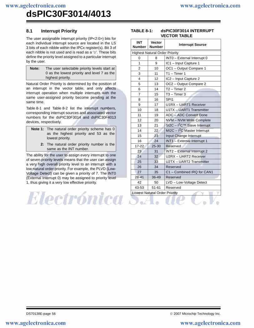
dsPIC30F3014/4013
DS70138E-page 56 © 2007 Microchip Technology Inc.
8.1 Interrupt Priority
The user assignable interrupt priority (IP<2:0>) bits foreach individual interrupt source are located in the LS3 bits of each nibble within the IPCx register(s). Bit 3 ofeach nibble is not used and is read as a ‘0’. These bitsdefine the priority level assigned to a particular interruptby the user.
Natural Order Priority is determined by the position ofan interrupt in the vector table, and only affectsinterrupt operation when multiple interrupts with thesame user-assigned priority become pending at thesame time.
Table 8-1 and Table 8-2 list the interrupt numbers,corresponding interrupt sources and associated vectornumbers for the dsPIC30F3014 and dsPIC30F4013devices, respectively.
The ability for the user to assign every interrupt to oneof seven priority levels means that the user can assigna very high overall priority level to an interrupt with alow natural order priority. For example, the PLVD (Low-Voltage Detect) can be given a priority of 7. The INT0(External Interrupt 0) may be assigned to priority level1, thus giving it a very low effective priority.
TABLE 8-1: dsPIC30F3014 INTERRUPT VECTOR TABLE
Note: The user selectable priority levels start at0 as the lowest priority and level 7 as thehighest priority.
Note 1: The natural order priority scheme has 0as the highest priority and 53 as thelowest priority.
2: The natural order priority number is thesame as the INT number.
INT Number
Vector Number
Interrupt Source
Highest Natural Order Priority
0 8 INT0 – External Interrupt 0
1 9 IC1 – Input Capture 1
2 10 OC1 – Output Compare 1
3 11 T1 – Timer 1
4 12 IC2 – Input Capture 2
5 13 OC2 – Output Compare 2
6 14 T2 – Timer 2
7 15 T3 – Timer 3
8 16 SPI1
9 17 U1RX – UART1 Receiver
10 18 U1TX – UART1 Transmitter
11 19 ADC – ADC Convert Done
12 20 NVM – NVM Write Complete
13 21 SI2C – I2C™ Slave Interrupt
14 22 MI2C – I2C Master Interrupt
15 23 Input Change Interrupt
16 24 INT1 – External Interrupt 1
17-22 25-30 Reserved
23 31 INT2 – External Interrupt 2
24 32 U2RX – UART2 Receiver
25 33 U2TX – UART2 Transmitter
26 34 Reserved
27 35 C1 – Combined IRQ for CAN1
28-41 36-49 Reserved
42 50 LVD – Low-Voltage Detect
43-53 51-61 Reserved
Lowest Natural Order Priority
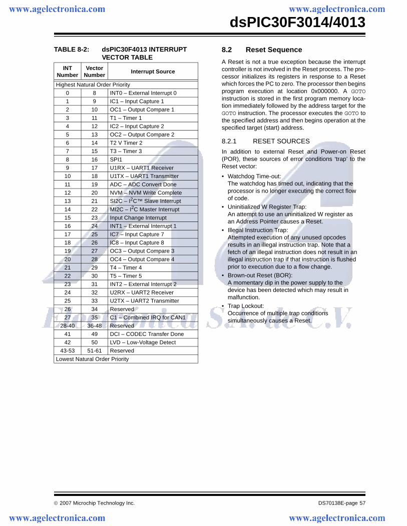
© 2007 Microchip Technology Inc. DS70138E-page 57
dsPIC30F3014/4013
TABLE 8-2: dsPIC30F4013 INTERRUPT VECTOR TABLE
8.2 Reset Sequence
A Reset is not a true exception because the interruptcontroller is not involved in the Reset process. The pro-cessor initializes its registers in response to a Resetwhich forces the PC to zero. The processor then beginsprogram execution at location 0x000000. A GOTOinstruction is stored in the first program memory loca-tion immediately followed by the address target for theGOTO instruction. The processor executes the GOTO tothe specified address and then begins operation at thespecified target (start) address.
8.2.1 RESET SOURCES
In addition to external Reset and Power-on Reset(POR), these sources of error conditions ‘trap’ to theReset vector:
• Watchdog Time-out:The watchdog has timed out, indicating that the processor is no longer executing the correct flow of code.
• Uninitialized W Register Trap:An attempt to use an uninitialized W register as an Address Pointer causes a Reset.
• Illegal Instruction Trap:Attempted execution of any unused opcodes results in an illegal instruction trap. Note that a fetch of an illegal instruction does not result in an illegal instruction trap if that instruction is flushed prior to execution due to a flow change.
• Brown-out Reset (BOR):A momentary dip in the power supply to the device has been detected which may result in malfunction.
• Trap Lockout:Occurrence of multiple trap conditions simultaneously causes a Reset.
INT Number
Vector Number
Interrupt Source
Highest Natural Order Priority
0 8 INT0 – External Interrupt 0
1 9 IC1 – Input Capture 1
2 10 OC1 – Output Compare 1
3 11 T1 – Timer 1
4 12 IC2 – Input Capture 2
5 13 OC2 – Output Compare 2
6 14 T2 V Timer 2
7 15 T3 – Timer 3
8 16 SPI1
9 17 U1RX – UART1 Receiver
10 18 U1TX – UART1 Transmitter
11 19 ADC – ADC Convert Done
12 20 NVM – NVM Write Complete
13 21 SI2C – I2C™ Slave Interrupt
14 22 MI2C – I2C Master Interrupt
15 23 Input Change Interrupt
16 24 INT1 – External Interrupt 1
17 25 IC7 – Input Capture 7
18 26 IC8 – Input Capture 8
19 27 OC3 – Output Compare 3
20 28 OC4 – Output Compare 4
21 29 T4 – Timer 4
22 30 T5 – Timer 5
23 31 INT2 – External Interrupt 2
24 32 U2RX – UART2 Receiver
25 33 U2TX – UART2 Transmitter
26 34 Reserved
27 35 C1 – Combined IRQ for CAN1
28-40 36-48 Reserved
41 49 DCI – CODEC Transfer Done
42 50 LVD – Low-Voltage Detect
43-53 51-61 Reserved
Lowest Natural Order Priority
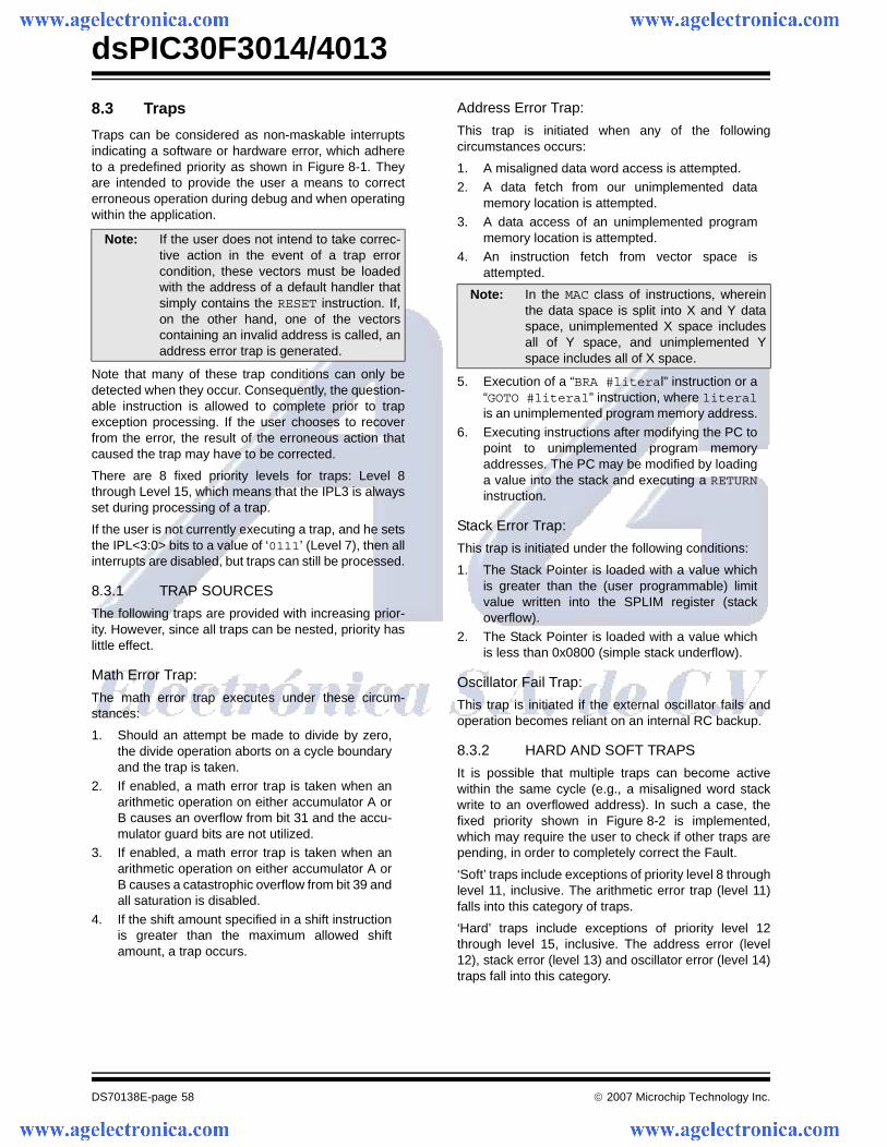
dsPIC30F3014/4013
DS70138E-page 58 © 2007 Microchip Technology Inc.
8.3 Traps
Traps can be considered as non-maskable interruptsindicating a software or hardware error, which adhereto a predefined priority as shown in Figure 8-1. Theyare intended to provide the user a means to correcterroneous operation during debug and when operatingwithin the application.
Note that many of these trap conditions can only bedetected when they occur. Consequently, the question-able instruction is allowed to complete prior to trapexception processing. If the user chooses to recoverfrom the error, the result of the erroneous action thatcaused the trap may have to be corrected.
There are 8 fixed priority levels for traps: Level 8through Level 15, which means that the IPL3 is alwaysset during processing of a trap.
If the user is not currently executing a trap, and he setsthe IPL<3:0> bits to a value of ‘0111’ (Level 7), then allinterrupts are disabled, but traps can still be processed.
8.3.1 TRAP SOURCES
The following traps are provided with increasing prior-ity. However, since all traps can be nested, priority haslittle effect.
Math Error Trap:
The math error trap executes under these circum-stances:
1. Should an attempt be made to divide by zero,the divide operation aborts on a cycle boundaryand the trap is taken.
2. If enabled, a math error trap is taken when anarithmetic operation on either accumulator A orB causes an overflow from bit 31 and the accu-mulator guard bits are not utilized.
3. If enabled, a math error trap is taken when anarithmetic operation on either accumulator A orB causes a catastrophic overflow from bit 39 andall saturation is disabled.
4. If the shift amount specified in a shift instructionis greater than the maximum allowed shiftamount, a trap occurs.
Address Error Trap:
This trap is initiated when any of the followingcircumstances occurs:
1. A misaligned data word access is attempted.2. A data fetch from our unimplemented data
memory location is attempted.3. A data access of an unimplemented program
memory location is attempted.4. An instruction fetch from vector space is
attempted.
5. Execution of a “BRA #literal” instruction or a“GOTO #literal” instruction, where literalis an unimplemented program memory address.
6. Executing instructions after modifying the PC topoint to unimplemented program memoryaddresses. The PC may be modified by loadinga value into the stack and executing a RETURNinstruction.
Stack Error Trap:
This trap is initiated under the following conditions:
1. The Stack Pointer is loaded with a value whichis greater than the (user programmable) limitvalue written into the SPLIM register (stackoverflow).
2. The Stack Pointer is loaded with a value whichis less than 0x0800 (simple stack underflow).
Oscillator Fail Trap:
This trap is initiated if the external oscillator fails andoperation becomes reliant on an internal RC backup.
8.3.2 HARD AND SOFT TRAPS
It is possible that multiple traps can become activewithin the same cycle (e.g., a misaligned word stackwrite to an overflowed address). In such a case, thefixed priority shown in Figure 8-2 is implemented,which may require the user to check if other traps arepending, in order to completely correct the Fault.
‘Soft’ traps include exceptions of priority level 8 throughlevel 11, inclusive. The arithmetic error trap (level 11)falls into this category of traps.
‘Hard’ traps include exceptions of priority level 12through level 15, inclusive. The address error (level12), stack error (level 13) and oscillator error (level 14)traps fall into this category.
Note: If the user does not intend to take correc-tive action in the event of a trap errorcondition, these vectors must be loadedwith the address of a default handler thatsimply contains the RESET instruction. If,on the other hand, one of the vectorscontaining an invalid address is called, anaddress error trap is generated.
Note: In the MAC class of instructions, whereinthe data space is split into X and Y dataspace, unimplemented X space includesall of Y space, and unimplemented Yspace includes all of X space.
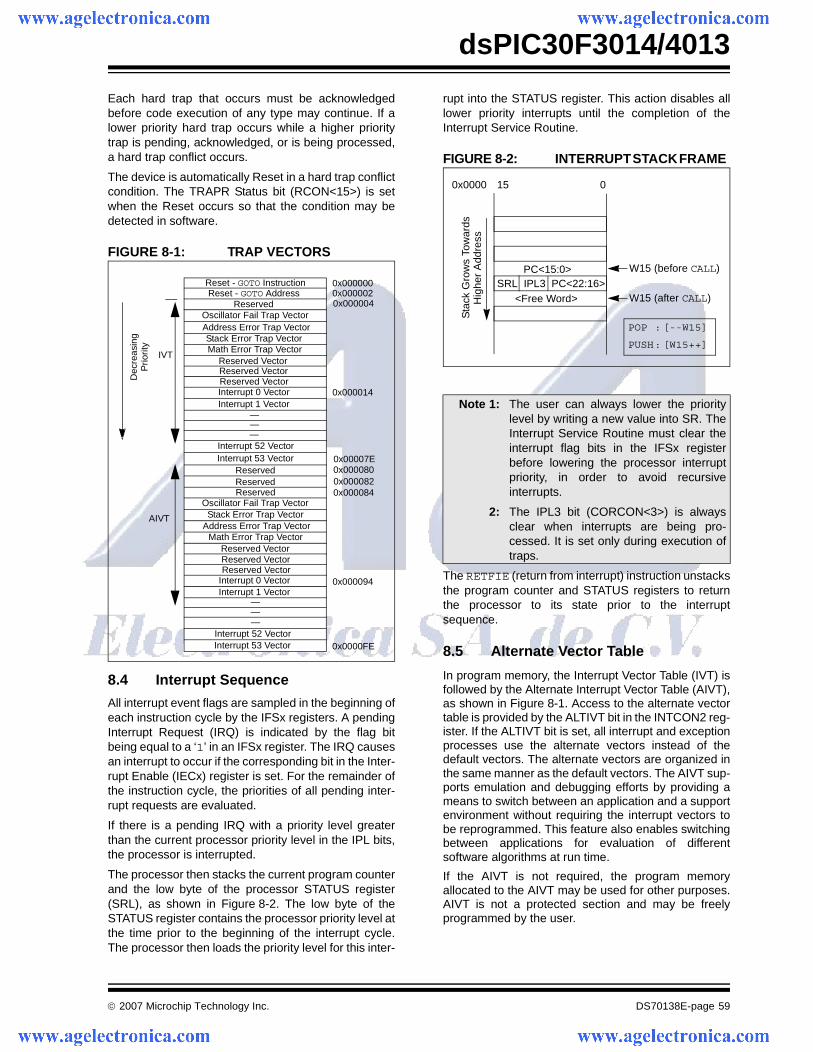
© 2007 Microchip Technology Inc. DS70138E-page 59
dsPIC30F3014/4013
Each hard trap that occurs must be acknowledgedbefore code execution of any type may continue. If alower priority hard trap occurs while a higher prioritytrap is pending, acknowledged, or is being processed,a hard trap conflict occurs.
The device is automatically Reset in a hard trap conflictcondition. The TRAPR Status bit (RCON<15>) is setwhen the Reset occurs so that the condition may bedetected in software.
FIGURE 8-1: TRAP VECTORS
8.4 Interrupt Sequence
All interrupt event flags are sampled in the beginning ofeach instruction cycle by the IFSx registers. A pendingInterrupt Request (IRQ) is indicated by the flag bitbeing equal to a ‘1’ in an IFSx register. The IRQ causesan interrupt to occur if the corresponding bit in the Inter-rupt Enable (IECx) register is set. For the remainder ofthe instruction cycle, the priorities of all pending inter-rupt requests are evaluated.
If there is a pending IRQ with a priority level greaterthan the current processor priority level in the IPL bits,the processor is interrupted.
The processor then stacks the current program counterand the low byte of the processor STATUS register(SRL), as shown in Figure 8-2. The low byte of theSTATUS register contains the processor priority level atthe time prior to the beginning of the interrupt cycle.The processor then loads the priority level for this inter-
rupt into the STATUS register. This action disables alllower priority interrupts until the completion of theInterrupt Service Routine.
FIGURE 8-2: INTERRUPT STACK FRAME
The RETFIE (return from interrupt) instruction unstacksthe program counter and STATUS registers to returnthe processor to its state prior to the interruptsequence.
8.5 Alternate Vector Table
In program memory, the Interrupt Vector Table (IVT) isfollowed by the Alternate Interrupt Vector Table (AIVT),as shown in Figure 8-1. Access to the alternate vectortable is provided by the ALTIVT bit in the INTCON2 reg-ister. If the ALTIVT bit is set, all interrupt and exceptionprocesses use the alternate vectors instead of thedefault vectors. The alternate vectors are organized inthe same manner as the default vectors. The AIVT sup-ports emulation and debugging efforts by providing ameans to switch between an application and a supportenvironment without requiring the interrupt vectors tobe reprogrammed. This feature also enables switchingbetween applications for evaluation of differentsoftware algorithms at run time.
If the AIVT is not required, the program memoryallocated to the AIVT may be used for other purposes.AIVT is not a protected section and may be freelyprogrammed by the user.
Address Error Trap Vector
Oscillator Fail Trap VectorStack Error Trap Vector
Reserved VectorMath Error Trap Vector
Reserved
Oscillator Fail Trap VectorAddress Error Trap Vector
Reserved VectorReserved Vector
Interrupt 0 VectorInterrupt 1 Vector
———
Interrupt 52 VectorInterrupt 53 Vector
Math Error Trap Vector
Dec
reas
ing
Prio
rity
0x000000
0x000014
Reserved
Stack Error Trap Vector
Reserved Vector
Interrupt 1 Vector
——
Interrupt 52 VectorInterrupt 53 Vector
IVT
AIVT
0x0000800x00007E
0x0000FE
Reserved
0x000094
Reset - GOTO InstructionReset - GOTO Address 0x000002
Reserved0x0000820x000084
0x000004
Reserved Vector
Reserved VectorInterrupt 0 Vector
—
Note 1: The user can always lower the prioritylevel by writing a new value into SR. TheInterrupt Service Routine must clear theinterrupt flag bits in the IFSx registerbefore lowering the processor interruptpriority, in order to avoid recursiveinterrupts.
2: The IPL3 bit (CORCON<3>) is alwaysclear when interrupts are being pro-cessed. It is set only during execution oftraps.
<Free Word>
015
W15 (before CALL)
W15 (after CALL)
Sta
ck G
row
s To
war
dsH
ighe
r A
ddre
ss
0x0000
PC<15:0> SRL IPL3 PC<22:16>
POP : [--W15]
PUSH: [W15++]
dsPIC30F3014/4013
DS70138E-page 60 © 2007 Microchip Technology Inc.
8.6 Fast Context SavingA context saving option is available using shadow reg-isters. Shadow registers are provided for the DC, N,OV, Z and C bits in SR, and the registers W0 throughW3. The shadows are only one level deep. The shadowregisters are accessible using the PUSH.S and POP.Sinstructions only.
When the processor vectors to an interrupt, thePUSH.S instruction can be used to store the currentvalue of the aforementioned registers into theirrespective shadow registers.
If an ISR of a certain priority uses the PUSH.S andPOP.S instructions for fast context saving, then ahigher priority ISR should not include the same instruc-tions. Users must save the key registers in softwareduring a lower priority interrupt if the higher priority ISRuses fast context saving.
8.7 External Interrupt Requests
The interrupt controller supports up to five externalinterrupt request signals, INT0-INT4. These inputs areedge sensitive; they require a low-to-high or a high-to-low transition to generate an interrupt request. TheINTCON2 register has three bits, INT0EP-INT2EP, thatselect the polarity of the edge detection circuitry.
8.8 Wake-up from Sleep and Idle
The interrupt controller may be used to wake-up theprocessor from either Sleep or Idle modes, if Sleep orIdle mode is active when the interrupt is generated.
If an enabled interrupt request of sufficient priority isreceived by the interrupt controller, then the standardinterrupt request is presented to the processor. At thesame time, the processor wakes up from Sleep or Idleand begins execution of the Interrupt Service Routine(ISR) needed to process the interrupt request.
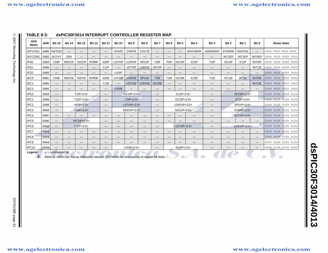
© 2007 M
icrochip Technology Inc.
DS
70138E-page 61
dsP
IC30F
3014/4013
TABLE 8-3: dsPIC30F3014 INTERRUPT CONTROLLER REGISTER MAP
SFR Name ADR Bit 15 Bit 14 Bit 13 Bit 12 Bit 11 Bit 10 Bit 9 Bit 8 Bit 7 Bit 6 Bit 5 Bit 4 Bit 3 Bit 2 Bit 1 Bit 0 Reset State
INTCON1 0080 NSTDIS — — — — OVATE OVBTE COVTE — — — MATHERR ADDRERR STKERR OSCFAIL — 0000 0000 0000 0000
INTCON2 0082 ALTIVT DISI — — — — — — — — — — — INT2EP INT1EP INT0EP 0000 0000 0000 0000
IFS0 0084 CNIF MI2CIF SI2CIF NVMIF ADIF U1TXIF U1RXIF SPI1IF T3IF T2IF OC2IF IC2IF T1IF OC1IF IC1IF INT0IF 0000 0000 0000 0000
IFS1 0086 — — — — C1IF — U2TXIF U2RXIF INT2IF — — — — — — INT1IF 0000 0000 0000 0000
IFS2 0088 — — — — — LVDIF — — — — — — — — — — 0000 0000 0000 0000
IEC0 008C CNIE MI2CIE SI2CIE NVMIE ADIE U1TXIE U1RXIE SPI1IE T3IE T2IE OC2IE IC2IE T1IE OC1IE IC1IE INT0IE 0000 0000 0000 0000
IEC1 008E — — — — C1IE — U2TXIE U2RXIE INT2IE — — — — — — INT1IE 0000 0000 0000 0000
IEC2 0090 — — — — — LVDIE — — — — — — — — — — 0000 0000 0000 0000
IPC0 0094 — T1IP<2:0> — OC1IP<2:0> — IC1IP<2:0> — INT0IP<2:0> 0100 0100 0100 0100
IPC1 0096 — T31P<2:0> — T2IP<2:0> — OC2IP<2:0> — IC2IP<2:0> 0100 0100 0100 0100
IPC2 0098 — ADIP<2:0> — U1TXIP<2:0> — U1RXIP<2:0> — SPI1IP<2:0> 0100 0100 0100 0100
IPC3 009A — CNIP<2:0> — MI2CIP<2:0> — SI2CIP<2:0> — NVMIP<2:0> 0100 0100 0100 0100
IPC4 009C — — — — — — — — — — — — — INT1IP<2:0> 0100 0100 0100 0100
IPC5 009E — INT2IP<2:0> — — — — — — — — — — — — 0100 0100 0100 0100
IPC6 00A0 — C1IP<2:0> — — — — — U2TXIP<2:0> — U2RXIP<2:0> 0100 0100 0100 0100
IPC7 00A2 — — — — — — — — — — — — — — — — 0100 0100 0100 0100
IPC8 00A4 — — — — — — — — — — — — — — — — 0100 0100 0100 0100
IPC9 00A6 — — — — — — — — — — — — — — — — 0000 0100 0100 0100
IPC10 00A8 — — — — — LVDIP<2:0> — DCIIP<2:0> — — — — 0000 0100 0100 0000
Legend: u = uninitialized bit
2: Refer to “dsPIC30F Family Reference Manual” (DS70046) for descriptions of register bit fields.
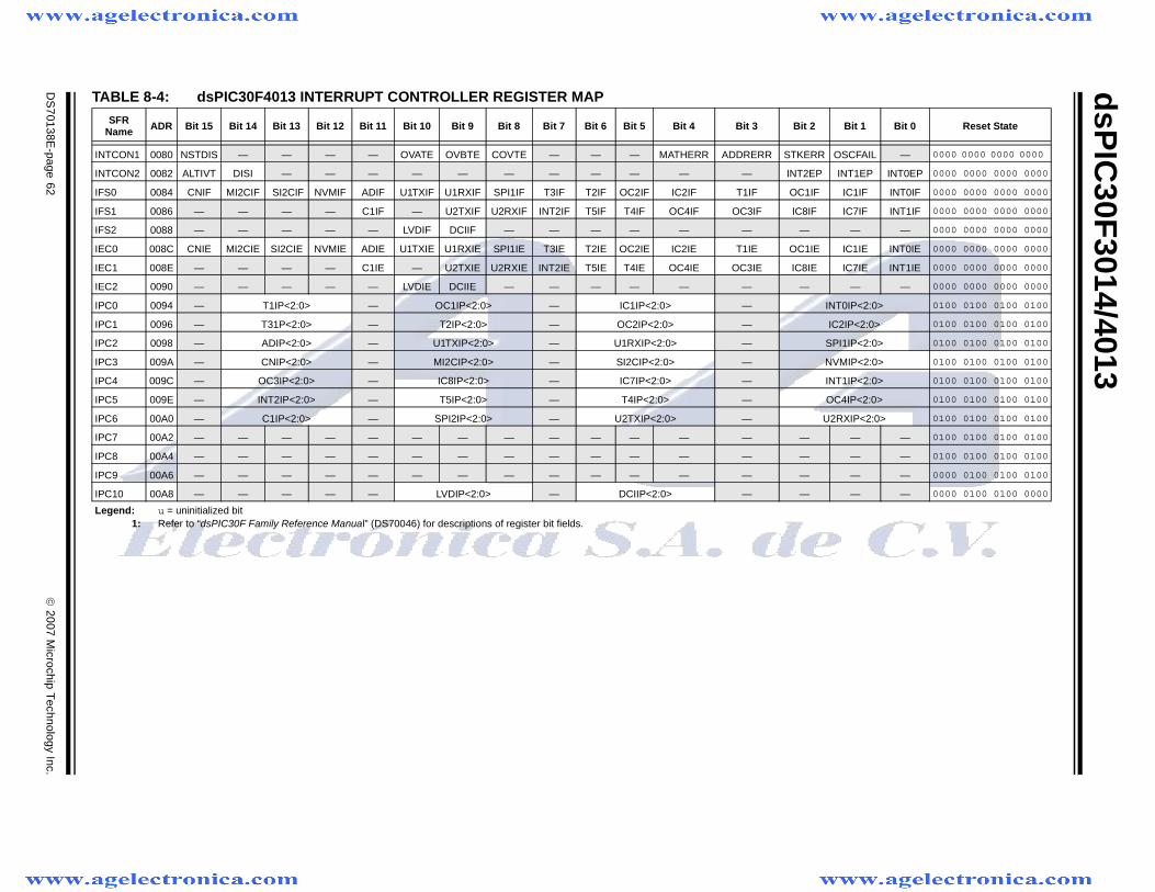
dsP
IC30F
3014/4013
DS
70138E-page 62
© 2007 M
icrochip Technology Inc.
TABLE 8-4: dsPIC30F4013 INTERRUPT CONTROLLER REGISTER MAP
SFR Name ADR Bit 15 Bit 14 Bit 13 Bit 12 Bit 11 Bit 10 Bit 9 Bit 8 Bit 7 Bit 6 Bit 5 Bit 4 Bit 3 Bit 2 Bit 1 Bit 0 Reset State
INTCON1 0080 NSTDIS — — — — OVATE OVBTE COVTE — — — MATHERR ADDRERR STKERR OSCFAIL — 0000 0000 0000 0000
INTCON2 0082 ALTIVT DISI — — — — — — — — — — — INT2EP INT1EP INT0EP 0000 0000 0000 0000
IFS0 0084 CNIF MI2CIF SI2CIF NVMIF ADIF U1TXIF U1RXIF SPI1IF T3IF T2IF OC2IF IC2IF T1IF OC1IF IC1IF INT0IF 0000 0000 0000 0000
IFS1 0086 — — — — C1IF — U2TXIF U2RXIF INT2IF T5IF T4IF OC4IF OC3IF IC8IF IC7IF INT1IF 0000 0000 0000 0000
IFS2 0088 — — — — — LVDIF DCIIF — — — — — — — — — 0000 0000 0000 0000
IEC0 008C CNIE MI2CIE SI2CIE NVMIE ADIE U1TXIE U1RXIE SPI1IE T3IE T2IE OC2IE IC2IE T1IE OC1IE IC1IE INT0IE 0000 0000 0000 0000
IEC1 008E — — — — C1IE — U2TXIE U2RXIE INT2IE T5IE T4IE OC4IE OC3IE IC8IE IC7IE INT1IE 0000 0000 0000 0000
IEC2 0090 — — — — — LVDIE DCIIE — — — — — — — — — 0000 0000 0000 0000
IPC0 0094 — T1IP<2:0> — OC1IP<2:0> — IC1IP<2:0> — INT0IP<2:0> 0100 0100 0100 0100
IPC1 0096 — T31P<2:0> — T2IP<2:0> — OC2IP<2:0> — IC2IP<2:0> 0100 0100 0100 0100
IPC2 0098 — ADIP<2:0> — U1TXIP<2:0> — U1RXIP<2:0> — SPI1IP<2:0> 0100 0100 0100 0100
IPC3 009A — CNIP<2:0> — MI2CIP<2:0> — SI2CIP<2:0> — NVMIP<2:0> 0100 0100 0100 0100
IPC4 009C — OC3IP<2:0> — IC8IP<2:0> — IC7IP<2:0> — INT1IP<2:0> 0100 0100 0100 0100
IPC5 009E — INT2IP<2:0> — T5IP<2:0> — T4IP<2:0> — OC4IP<2:0> 0100 0100 0100 0100
IPC6 00A0 — C1IP<2:0> — SPI2IP<2:0> — U2TXIP<2:0> — U2RXIP<2:0> 0100 0100 0100 0100
IPC7 00A2 — — — — — — — — — — — — — — — — 0100 0100 0100 0100
IPC8 00A4 — — — — — — — — — — — — — — — — 0100 0100 0100 0100
IPC9 00A6 — — — — — — — — — — — — — — — — 0000 0100 0100 0100
IPC10 00A8 — — — — — LVDIP<2:0> — DCIIP<2:0> — — — — 0000 0100 0100 0000
Legend: u = uninitialized bit1: Refer to “dsPIC30F Family Reference Manual” (DS70046) for descriptions of register bit fields.
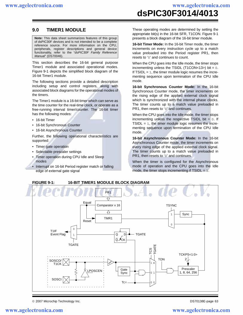
© 2007 Microchip Technology Inc. DS70138E-page 63
dsPIC30F3014/4013
9.0 TIMER1 MODULE
This section describes the 16-bit general purposeTimer1 module and associated operational modes.Figure 9-1 depicts the simplified block diagram of the16-bit Timer1 module.
The following sections provide a detailed descriptionincluding setup and control registers, along withassociated block diagrams for the operational modes ofthe timers.
The Timer1 module is a 16-bit timer which can serve asthe time counter for the real-time clock, or operate as afree-running interval timer/counter. The 16-bit timerhas the following modes:
• 16-bit Timer• 16-bit Synchronous Counter• 16-bit Asynchronous Counter
Further, the following operational characteristics aresupported:
• Timer gate operation• Selectable prescaler settings
• Timer operation during CPU Idle and Sleep modes
• Interrupt on 16-bit Period register match or falling edge of external gate signal
These operating modes are determined by setting theappropriate bit(s) in the 16-bit SFR, T1CON. Figure 9-1presents a block diagram of the 16-bit timer module.
16-bit Timer Mode: In the 16-bit Timer mode, the timerincrements on every instruction cycle up to a matchvalue preloaded into the Period register PR1, thenresets to ‘0’ and continues to count.
When the CPU goes into the Idle mode, the timer stopsincrementing unless the TSIDL (T1CON<13>) bit = 0.If TSIDL = 1, the timer module logic resumes the incre-menting sequence upon termination of the CPU Idlemode.
16-bit Synchronous Counter Mode: In the 16-bitSynchronous Counter mode, the timer increments onthe rising edge of the applied external clock signalwhich is synchronized with the internal phase clocks.The timer counts up to a match value preloaded inPR1, then resets to ‘0’ and continues.
When the CPU goes into the Idle mode, the timer stopsincrementing unless the respective TSIDL bit = 0. IfTSIDL = 1, the timer module logic resumes the incre-menting sequence upon termination of the CPU Idlemode.
16-bit Asynchronous Counter Mode: In the 16-bitAsynchronous Counter mode, the timer increments onevery rising edge of the applied external clock signal.The timer counts up to a match value preloaded inPR1, then resets to ‘0’ and continues.
When the timer is configured for the Asynchronousmode of operation and the CPU goes into the Idlemode, the timer stops incrementing if TSIDL = 1.
FIGURE 9-1: 16-BIT TIMER1 MODULE BLOCK DIAGRAM
Note: This data sheet summarizes features of this groupof dsPIC30F devices and is not intended to be a completereference source. For more information on the CPU,peripherals, register descriptions and general devicefunctionality, refer to the “dsPIC30F Family ReferenceManual” (DS70046).
TON
Sync
SOSCI
SOSCO/
PR1
T1IF
EqualComparator x 16
TMR1Reset
LPOSCEN
Event Flag
1
0
TSYNC
Q
Q D
CK
TGATE
TCKPS<1:0>
Prescaler1, 8, 64, 256
2
TGATE
TCY
1
0
T1CK
TC
S
1 x
0 1
TG
AT
E
0 0
GateSync
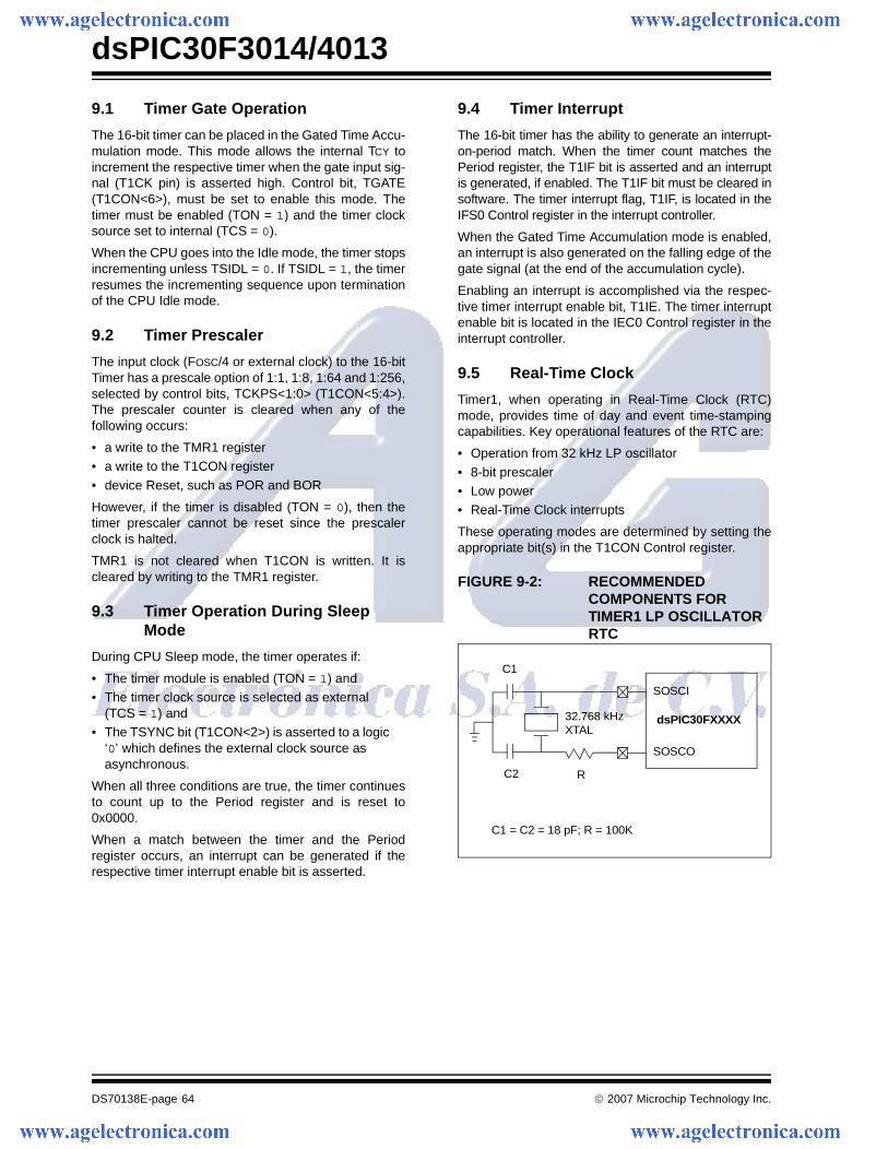
dsPIC30F3014/4013
DS70138E-page 64 © 2007 Microchip Technology Inc.
9.1 Timer Gate Operation
The 16-bit timer can be placed in the Gated Time Accu-mulation mode. This mode allows the internal TCY toincrement the respective timer when the gate input sig-nal (T1CK pin) is asserted high. Control bit, TGATE(T1CON<6>), must be set to enable this mode. Thetimer must be enabled (TON = 1) and the timer clocksource set to internal (TCS = 0).
When the CPU goes into the Idle mode, the timer stopsincrementing unless TSIDL = 0. If TSIDL = 1, the timerresumes the incrementing sequence upon terminationof the CPU Idle mode.
9.2 Timer Prescaler
The input clock (FOSC/4 or external clock) to the 16-bitTimer has a prescale option of 1:1, 1:8, 1:64 and 1:256,selected by control bits, TCKPS<1:0> (T1CON<5:4>).The prescaler counter is cleared when any of thefollowing occurs:
• a write to the TMR1 register• a write to the T1CON register
• device Reset, such as POR and BOR
However, if the timer is disabled (TON = 0), then thetimer prescaler cannot be reset since the prescalerclock is halted.
TMR1 is not cleared when T1CON is written. It iscleared by writing to the TMR1 register.
9.3 Timer Operation During Sleep Mode
During CPU Sleep mode, the timer operates if:
• The timer module is enabled (TON = 1) and • The timer clock source is selected as external
(TCS = 1) and• The TSYNC bit (T1CON<2>) is asserted to a logic
‘0’ which defines the external clock source as asynchronous.
When all three conditions are true, the timer continuesto count up to the Period register and is reset to0x0000.
When a match between the timer and the Periodregister occurs, an interrupt can be generated if therespective timer interrupt enable bit is asserted.
9.4 Timer Interrupt
The 16-bit timer has the ability to generate an interrupt-on-period match. When the timer count matches thePeriod register, the T1IF bit is asserted and an interruptis generated, if enabled. The T1IF bit must be cleared insoftware. The timer interrupt flag, T1IF, is located in theIFS0 Control register in the interrupt controller.
When the Gated Time Accumulation mode is enabled,an interrupt is also generated on the falling edge of thegate signal (at the end of the accumulation cycle).
Enabling an interrupt is accomplished via the respec-tive timer interrupt enable bit, T1IE. The timer interruptenable bit is located in the IEC0 Control register in theinterrupt controller.
9.5 Real-Time Clock
Timer1, when operating in Real-Time Clock (RTC)mode, provides time of day and event time-stampingcapabilities. Key operational features of the RTC are:
• Operation from 32 kHz LP oscillator
• 8-bit prescaler• Low power • Real-Time Clock interrupts
These operating modes are determined by setting theappropriate bit(s) in the T1CON Control register.
FIGURE 9-2: RECOMMENDED COMPONENTS FOR TIMER1 LP OSCILLATOR RTC
SOSCI
SOSCO
R
C1
C2
dsPIC30FXXXX32.768 kHzXTAL
C1 = C2 = 18 pF; R = 100K
© 2007 Microchip Technology Inc. DS70138E-page 65
dsPIC30F3014/4013
9.5.1 RTC OSCILLATOR OPERATION
When the TON = 1, TCS = 1 and TGATE = 0, the timerincrements on the rising edge of the 32 kHz LP oscilla-tor output signal, up to the value specified in the Periodregister and is then reset to ‘0’.
The TSYNC bit must be asserted to a logic ‘0’(Asynchronous mode) for correct operation.
Enabling LPOSCEN (OSCCON<1>) disables the nor-mal Timer and Counter modes and enable a timercarry-out wake-up event.
When the CPU enters Sleep mode, the RTC continuesto operate, provided the 32 kHz external crystal oscilla-tor is active and the control bits have not beenchanged. The TSIDL bit should be cleared to ‘0’ inorder for RTC to continue operation in Idle mode.
9.5.2 RTC INTERRUPTS
When an interrupt event occurs, the respective interruptflag, T1IF, is asserted and an interrupt is generated, ifenabled. The T1IF bit must be cleared in software. Therespective Timer interrupt flag, T1IF, is located in theIFS0 STATUS register in the interrupt controller.
Enabling an interrupt is accomplished via the respec-tive timer interrupt enable bit, T1IE. The timer interruptenable bit is located in the IEC0 Control register in theinterrupt controller.

dsP
IC30F
3014/4013
DS
70138E-page 66
© 2007 M
icrochip Technology Inc.
TABLE 9-1: dsPIC30F3014/4013 TIMER1 REGISTER MAP
SFR Name Addr. Bit 15 Bit 14 Bit 13 Bit 12 Bit 11 Bit 10 Bit 9 Bit 8 Bit 7 Bit 6 Bit 5 Bit 4 Bit 3 Bit 2 Bit 1 Bit 0 Reset State
TMR1 0100 Timer1 Register uuuu uuuu uuuu uuuu
PR1 0102 Period Register 1 1111 1111 1111 1111
T1CON 0104 TON — TSIDL — — — — — — TGATE TCKPS1 TCKPS0 — TSYNC TCS — 0000 0000 0000 0000
Legend: u = uninitialized bit2: Refer to “dsPIC30F Family Reference Manual” (DS70046) for descriptions of register bit fields.
© 2007 Microchip Technology Inc. DS70138E-page 67
dsPIC30F3014/4013
10.0 TIMER2/3 MODULE
This section describes the 32-bit general purposeTimer module (Timer2/3) and associated operationalmodes. Figure 10-1 depicts the simplified block dia-gram of the 32-bit Timer2/3 module. Figure 10-2 andFigure 10-3 show Timer2/3 configured as twoindependent 16-bit timers, Timer2 and Timer3,respectively.
The Timer2/3 module is a 32-bit timer (which can beconfigured as two 16-bit timers) with selectableoperating modes. These timers are utilized by otherperipheral modules, such as:
• Input Capture• Output Compare/Simple PWM
The following sections provide a detailed description,including setup and control registers, along withassociated block diagrams for the operational modes ofthe timers.
The 32-bit timer has the following modes:
• Two independent 16-bit timers (Timer2 and Timer3) with all 16-bit operating modes (except Asynchronous Counter mode)
• Single 32-bit timer operation• Single 32-bit synchronous counter
Further, the following operational characteristics aresupported:
• ADC event trigger• Timer gate operation• Selectable prescaler settings
• Timer operation during Idle and Sleep modes• Interrupt on a 32-bit period register match
These operating modes are determined by setting theappropriate bit(s) in the 16-bit T2CON and T3CONSFRs.
For 32-bit timer/counter operation, Timer2 is the lswand Timer3 is the msw of the 32-bit timer.
16-bit Timer Mode: In the 16-bit mode, Timer2 andTimer3 can be configured as two independent 16-bittimers. Each timer can be set up in either 16-bit Timermode or 16-bit Synchronous Counter mode. SeeSection 9.0 “Timer1 Module” for details on these twooperating modes.
The only functional difference between Timer2 andTimer3 is that Timer2 provides synchronization of theclock prescaler output. This is useful for high-frequencyexternal clock inputs.
32-bit Timer Mode: In the 32-bit Timer mode, the timerincrements on every instruction cycle, up to a matchvalue preloaded into the combined 32-bit Periodregister, PR3/PR2, then resets to ‘0’ and continues tocount.
For synchronous 32-bit reads of the Timer2/Timer3pair, reading the lsw (TMR2 register) causes the mswto be read and latched into a 16-bit holding register,termed TMR3HLD.
For synchronous 32-bit writes, the holding register(TMR3HLD) must first be written to. When followed bya write to the TMR2 register, the contents of TMR3HLDis transferred and latched into the MSB of the 32-bittimer (TMR3).
32-bit Synchronous Counter Mode: In the 32-bitSynchronous Counter mode, the timer increments onthe rising edge of the applied external clock signalwhich is synchronized with the internal phase clocks.The timer counts up to a match value preloaded in thecombined 32-bit period register, PR3/PR2, then resetsto ‘0’ and continues.
When the timer is configured for the SynchronousCounter mode of operation and the CPU goes into theIdle mode, the timer stops incrementing unless theTSIDL (T2CON<13>) bit = 0. If TSIDL = 1, the timermodule logic resumes the incrementing sequenceupon termination of the CPU Idle mode.
Note: This data sheet summarizes features of this groupof dsPIC30F devices and is not intended to be a completereference source. For more information on the CPU,peripherals, register descriptions and general devicefunctionality, refer to the “dsPIC30F Family ReferenceManual” (DS70046).
Note: For 32-bit timer operation, T3CON controlbits are ignored. Only T2CON control bitsare used for setup and control. Timer2clock and gate inputs are utilized for the32-bit timer module, but an interrupt isgenerated with the Timer3 interrupt flag(T3IF) and the interrupt is enabled with theTimer3 interrupt enable bit (T3IE).
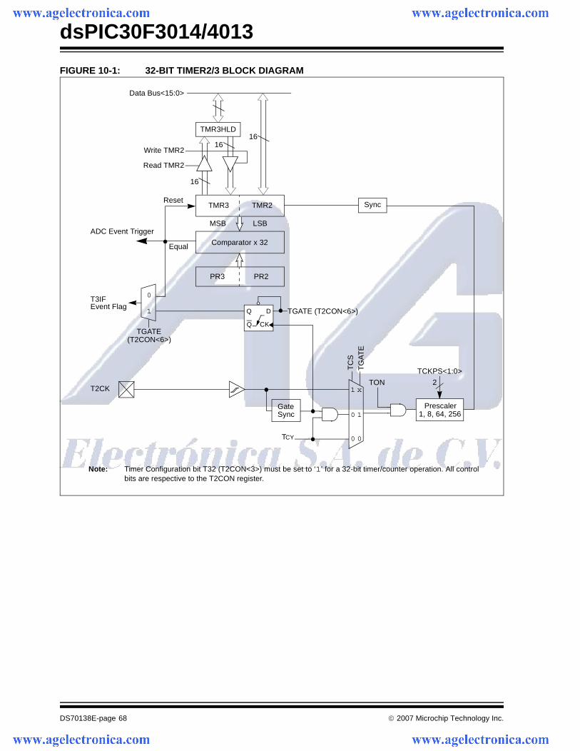
dsPIC30F3014/4013
DS70138E-page 68 © 2007 Microchip Technology Inc.
FIGURE 10-1: 32-BIT TIMER2/3 BLOCK DIAGRAM
TMR3 TMR2
T3IF
Equal Comparator x 32
PR3 PR2
Reset
LSB MSB
Event Flag
Note: Timer Configuration bit T32 (T2CON<3>) must be set to ‘1’ for a 32-bit timer/counter operation. All controlbits are respective to the T2CON register.
Data Bus<15:0>
Read TMR2
Write TMR216
16
16
Q
Q D
CK
TGATE (T2CON<6>)
(T2CON<6>)TGATE
0
1
TON
TCKPS<1:0>
2
TCY
T
CS
1 x
0 1
TG
AT
E
0 0
Gate
T2CK
Sync
ADC Event Trigger
Sync
TMR3HLD
Prescaler1, 8, 64, 256
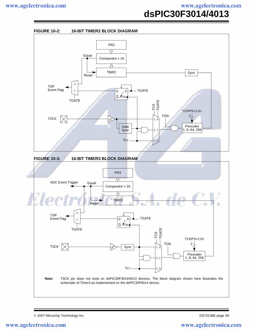
© 2007 Microchip Technology Inc. DS70138E-page 69
dsPIC30F3014/4013
FIGURE 10-2: 16-BIT TIMER2 BLOCK DIAGRAM
FIGURE 10-3: 16-BIT TIMER3 BLOCK DIAGRAM
TON
Sync
PR2
T2IF
EqualComparator x 16
TMR2Reset
Event Flag TGATE
TCKPS<1:0>
2
TGATE
TCY
1
0
TC
S
1 x
0 1
TG
AT
E
0 0
Gate
T2CK
SyncPrescaler
1, 8, 64, 256
Q
Q D
CK
TON
PR3
T3IF
EqualComparator x 16
TMR3Reset
Event Flag TGATE
TCKPS<1:0>
2
TGATE
TCY
1
0
TC
S
1 x
0 1
TG
AT
E
0 0
T3CK
ADC Event Trigger
Sync
Q
Q D
CK
Prescaler1, 8, 64, 256
Note: T3CK pin does not exist on dsPIC30F3014/4013 devices. The block diagram shown here illustrates theschematic of Timer3 as implemented on the dsPIC30F6014 device.
dsPIC30F3014/4013
DS70138E-page 70 © 2007 Microchip Technology Inc.
10.1 Timer Gate Operation
The 32-bit timer can be placed in the Gated Time Accu-mulation mode. This mode allows the internal TCY toincrement the respective timer when the gate inputsignal (T2CK pin) is asserted high. Control bit, TGATE(T2CON<6>), must be set to enable this mode. Whenin this mode, Timer2 is the originating clock source.The TGATE setting is ignored for Timer3. The timermust be enabled (TON = 1) and the timer clock sourceset to internal (TCS = 0).
The falling edge of the external signal terminates thecount operation but does not reset the timer. The usermust reset the timer in order to start counting from zero.
10.2 ADC Event Trigger
When a match occurs between the 32-bit timer (TMR3/TMR2) and the 32-bit combined period register (PR3/PR2), a special ADC trigger event signal is generatedby Timer3.
10.3 Timer Prescaler
The input clock (FOSC/4 or external clock) to the timerhas a prescale option of 1:1, 1:8, 1:64, and 1:256,selected by control bits, TCKPS<1:0> (T2CON<5:4>and T3CON<5:4>). For the 32-bit timer operation, theoriginating clock source is Timer2. The prescaler oper-ation for Timer3 is not applicable in this mode. Theprescaler counter is cleared when any of the followingoccurs:
• a write to the TMR2/TMR3 register• a write to the T2CON/T3CON register• device Reset, such as POR and BOR
However, if the timer is disabled (TON = 0), then theTimer 2 prescaler cannot be reset since the prescalerclock is halted.
TMR2/TMR3 is not cleared when T2CON/T3CON iswritten.
10.4 Timer Operation During Sleep Mode
During CPU Sleep mode, the timer does not operatebecause the internal clocks are disabled.
10.5 Timer Interrupt
The 32-bit timer module can generate an interrupt-on-period match or on the falling edge of the external gatesignal. When the 32-bit timer count matches therespective 32-bit period register, or the falling edge ofthe external “gate” signal is detected, the T3IF bit(IFS0<7>) is asserted and an interrupt is generated, ifenabled. In this mode, the T3IF interrupt flag is used asthe source of the interrupt. The T3IF bit must becleared in software.
Enabling an interrupt is accomplished via therespective timer interrupt enable bit, T3IE (IEC0<7>).

© 2007 M
icrochip Technology Inc.
DS
70138E-page 71
dsP
IC30F
3014/4013
TABLE 10-1: dsPIC30F3014/4013 TIMER2/3 REGISTER MAP
SFR Name Addr. Bit 15 Bit 14 Bit 13 Bit 12 Bit 11 Bit 10 Bit 9 Bit 8 Bit 7 Bit 6 Bit 5 Bit 4 Bit 3 Bit 2 Bit 1 Bit 0 Reset State
TMR2 0106 Timer2 Register uuuu uuuu uuuu uuuu
TMR3HLD 0108 Timer3 Holding Register (for 32-bit timer operations only) uuuu uuuu uuuu uuuu
TMR3 010A Timer3 Register uuuu uuuu uuuu uuuu
PR2 010C Period Register 2 1111 1111 1111 1111
PR3 010E Period Register 3 1111 1111 1111 1111
T2CON 0110 TON — TSIDL — — — — — — TGATE TCKPS1 TCKPS0 T32 — TCS — 0000 0000 0000 0000
T3CON 0112 TON — TSIDL — — — — — — TGATE TCKPS1 TCKPS0 — — TCS — 0000 0000 0000 0000
Legend: u = uninitialized bit3: Refer to “dsPIC30F Family Reference Manual” (DS70046) for descriptions of register bit fields.

dsPIC30F3014/4013
DS70138E-page 72 © 2007 Microchip Technology Inc.
NOTES:
© 2007 Microchip Technology Inc. DS70138E-page 73
dsPIC30F3014/4013
11.0 TIMER4/5 MODULE
This section describes the second 32-bit generalpurpose Timer module (Timer4/5) and associatedoperational modes. Figure 11-1 depicts the simplifiedblock diagram of the 32-bit Timer4/5 module.Figure 11-2 and Figure 11-3 show Timer4/5 configuredas two independent 16-bit timers, Timer4 and Timer5,respectively.
The Timer4/5 module is similar in operation to theTimer2/3 module. However, there are somedifferences which are listed:
• The Timer4/5 module does not support the ADC event trigger feature
• Timer4/5 can not be utilized by other peripheral modules, such as input capture and output compare
The operating modes of the Timer4/5 module are deter-mined by setting the appropriate bit(s) in the 16-bitT4CON and T5CON SFRs.
For 32-bit timer/counter operation, Timer4 is the lswand Timer5 is the msw of the 32-bit timer.
FIGURE 11-1: 32-BIT TIMER4/5 BLOCK DIAGRAM
Note: This data sheet summarizes features of this groupof dsPIC30F devices and is not intended to be a completereference source. For more information on the CPU,peripherals, register descriptions and general devicefunctionality, refer to the dsPIC30F Family ReferenceManual (DS70046). Note: For 32-bit timer operation, T5CON control
bits are ignored. Only T4CON control bitsare used for setup and control. Timer4clock and gate inputs are utilized for the32-bit timer module but an interrupt isgenerated with the Timer5 interrupt flag(T5IF) and the interrupt is enabled with theTimer5 interrupt enable bit (T5IE).
TMR5 TMR4
T5IF
EqualComparator x 32
PR5 PR4
Reset
LSB MSB
Event Flag
Note: Timer Configuration bit T32 (T4CON<3>) must be set to ‘1’ for a 32-bit timer/counter operation. All controlbits are respective to the T4CON register.
Data Bus<15:0>
TMR5HLD
Read TMR4
Write TMR416
16
16
Q
Q D
CK
TGATE (T4CON<6>)
(T4CON<6>)TGATE
0
1
TON
TCKPS<1:0>
Prescaler1, 8, 64, 256
2
TCY
TC
S
1 x
0 1
TG
AT
E
0 0
Gate
T4CK
Sync
Sync
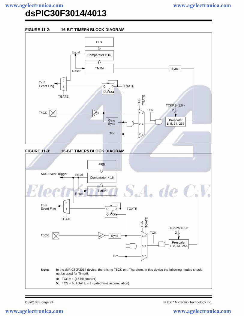
dsPIC30F3014/4013
DS70138E-page 74 © 2007 Microchip Technology Inc.
FIGURE 11-2: 16-BIT TIMER4 BLOCK DIAGRAM
FIGURE 11-3: 16-BIT TIMER5 BLOCK DIAGRAM
TON
Sync
PR4
T4IF
EqualComparator x 16
TMR4Reset
Event Flag TGATE
TCKPS<1:0>
Prescaler1, 8, 64, 256
2
TGATE
TCY
1
0
TC
S
1 x
0 1
TG
AT
E
0 0
Gate
T4CK
Sync
Q
Q D
CK
TON
PR5
T5IF
EqualComparator x 16
TMR5Reset
Event Flag TGATE
TCKPS<1:0>
Prescaler1, 8, 64, 256
2
TGATE
TCY
1
0
TC
S
1 x
0 1
TG
AT
E
0 0
T5CK
ADC Event Trigger
Sync
Q
Q D
CK
Note: In the dsPIC30F3014 device, there is no T5CK pin. Therefore, in this device the following modes should not be used for Timer5:
4: TCS = 1 (16-bit counter)5: TCS = 0, TGATE = 1 (gated time accumulation)
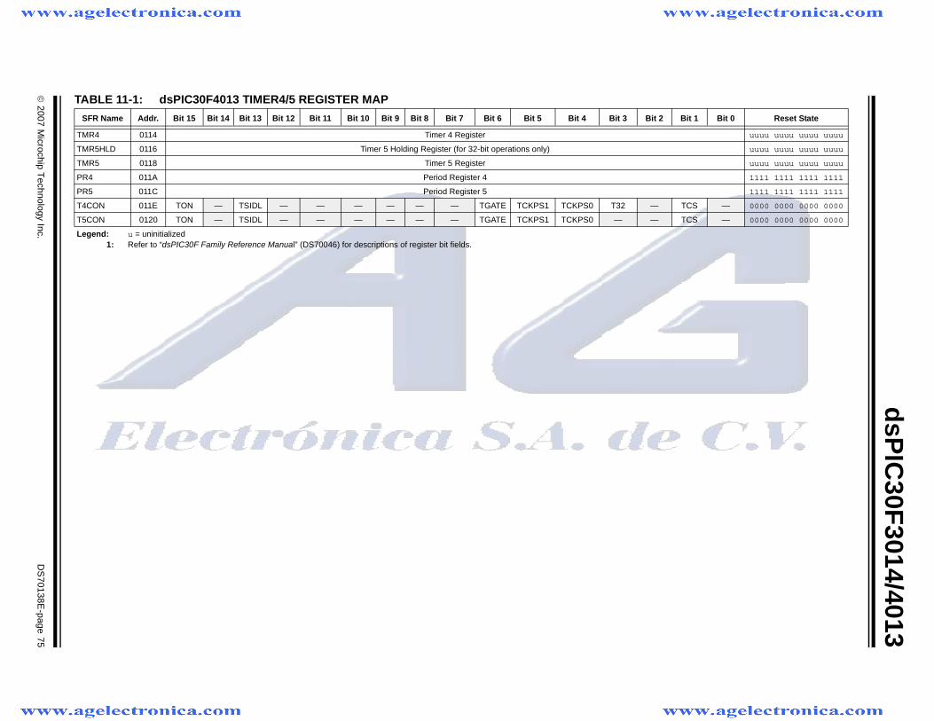
© 2007 M
icrochip Technology Inc.
DS
70138E-page 75
dsP
IC30F
3014/4013
TABLE 11-1: dsPIC30F4013 TIMER4/5 REGISTER MAP
SFR Name Addr. Bit 15 Bit 14 Bit 13 Bit 12 Bit 11 Bit 10 Bit 9 Bit 8 Bit 7 Bit 6 Bit 5 Bit 4 Bit 3 Bit 2 Bit 1 Bit 0 Reset State
TMR4 0114 Timer 4 Register uuuu uuuu uuuu uuuu
TMR5HLD 0116 Timer 5 Holding Register (for 32-bit operations only) uuuu uuuu uuuu uuuu
TMR5 0118 Timer 5 Register uuuu uuuu uuuu uuuu
PR4 011A Period Register 4 1111 1111 1111 1111
PR5 011C Period Register 5 1111 1111 1111 1111
T4CON 011E TON — TSIDL — — — — — — TGATE TCKPS1 TCKPS0 T32 — TCS — 0000 0000 0000 0000
T5CON 0120 TON — TSIDL — — — — — — TGATE TCKPS1 TCKPS0 — — TCS — 0000 0000 0000 0000
Legend: u = uninitialized1: Refer to “dsPIC30F Family Reference Manual” (DS70046) for descriptions of register bit fields.

dsPIC30F3014/4013
DS70138E-page 76 © 2007 Microchip Technology Inc.
NOTES:
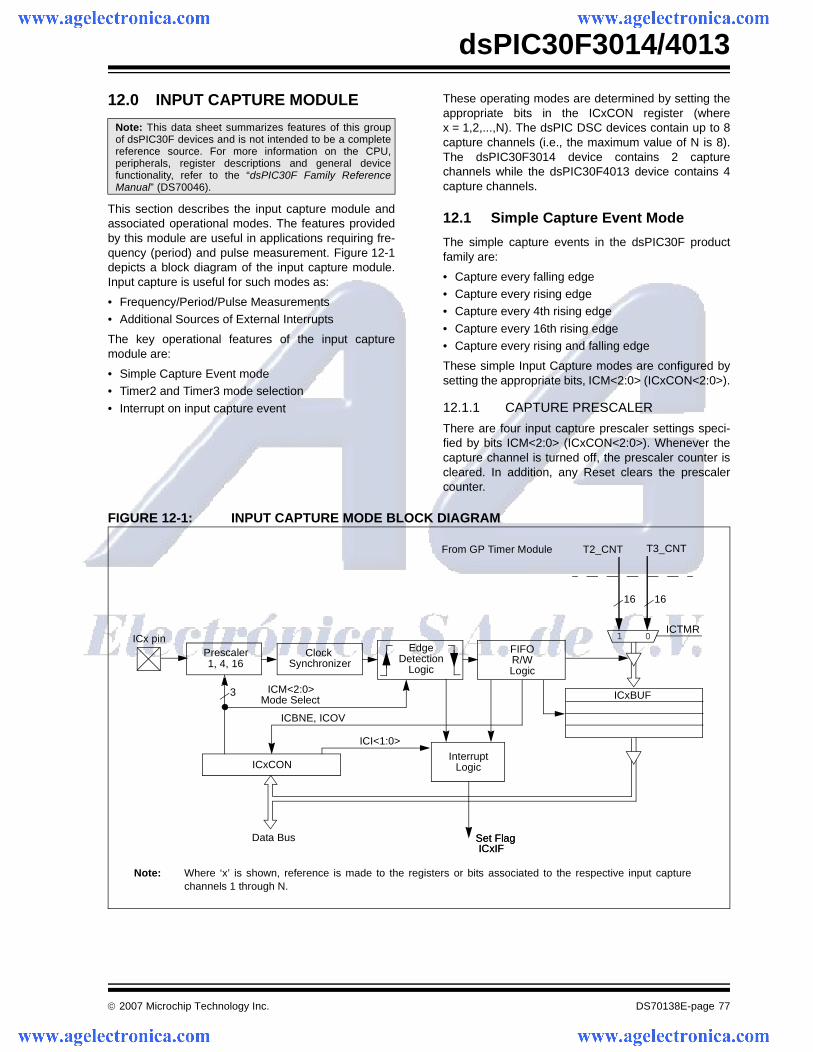
© 2007 Microchip Technology Inc. DS70138E-page 77
dsPIC30F3014/4013
12.0 INPUT CAPTURE MODULE
This section describes the input capture module andassociated operational modes. The features providedby this module are useful in applications requiring fre-quency (period) and pulse measurement. Figure 12-1depicts a block diagram of the input capture module.Input capture is useful for such modes as:
• Frequency/Period/Pulse Measurements• Additional Sources of External Interrupts
The key operational features of the input capturemodule are:
• Simple Capture Event mode• Timer2 and Timer3 mode selection
• Interrupt on input capture event
These operating modes are determined by setting theappropriate bits in the ICxCON register (wherex = 1,2,...,N). The dsPIC DSC devices contain up to 8capture channels (i.e., the maximum value of N is 8).The dsPIC30F3014 device contains 2 capturechannels while the dsPIC30F4013 device contains 4capture channels.
12.1 Simple Capture Event Mode
The simple capture events in the dsPIC30F productfamily are:
• Capture every falling edge• Capture every rising edge• Capture every 4th rising edge
• Capture every 16th rising edge• Capture every rising and falling edge
These simple Input Capture modes are configured bysetting the appropriate bits, ICM<2:0> (ICxCON<2:0>).
12.1.1 CAPTURE PRESCALER
There are four input capture prescaler settings speci-fied by bits ICM<2:0> (ICxCON<2:0>). Whenever thecapture channel is turned off, the prescaler counter iscleared. In addition, any Reset clears the prescalercounter.
FIGURE 12-1: INPUT CAPTURE MODE BLOCK DIAGRAM
Note: This data sheet summarizes features of this groupof dsPIC30F devices and is not intended to be a completereference source. For more information on the CPU,peripherals, register descriptions and general devicefunctionality, refer to the “dsPIC30F Family ReferenceManual” (DS70046).
ICxBUF
PrescalerICx pin
ICM<2:0>Mode Select
3
Note: Where ‘x’ is shown, reference is made to the registers or bits associated to the respective input capturechannels 1 through N.
1 0
Set Flag ICxIF
ICTMR
T2_CNT T3_CNT
EdgeDetection
Logic
ClockSynchronizer1, 4, 16
From GP Timer Module
16 16
FIFOR/WLogic
ICI<1:0>
ICBNE, ICOV
ICxCONInterrupt
Logic
Set Flag ICxIF
Data Bus
dsPIC30F3014/4013
DS70138E-page 78 © 2007 Microchip Technology Inc.
12.1.2 CAPTURE BUFFER OPERATION
Each capture channel has an associated FIFO bufferwhich is four 16-bit words deep. There are two statusflags which provide status on the FIFO buffer:
• ICBNE – Input Capture Buffer Not Empty• ICOV – Input Capture Overflow
The ICBFNE is set on the first input capture event andremain set until all capture events have been read fromthe FIFO. As each word is read from the FIFO, theremaining words are advanced by one position withinthe buffer.
In the event that the FIFO is full with four captureevents and a fifth capture event occurs prior to a readof the FIFO, an overflow condition occurs and the ICOVbit is set to a logic ‘1’. The fifth capture event is lost andis not stored in the FIFO. No additional events arecaptured until all four events have been read from thebuffer.
If a FIFO read is performed after the last read and nonew capture event has been received, the read willyield indeterminate results.
12.1.3 TIMER2 AND TIMER3 SELECTION MODE
The input capture module consists of up to 8 input cap-ture channels. Each channel can select between one oftwo timers for the time base, Timer2 or Timer3.
Selection of the timer resource is accomplishedthrough SFR bit, ICTMR (ICxCON<7>). Timer3 is thedefault timer resource available for the input capturemodule.
12.1.4 HALL SENSOR MODE
When the input capture module is set for capture onevery edge, rising and falling, ICM<2:0> = 001, thefollowing operations are performed by the input capturelogic:
• The input capture interrupt flag is set on every edge, rising and falling.
• The interrupt on Capture mode setting bits, ICI<1:0>, is ignored since every capture generates an interrupt.
• A capture overflow condition is not generated in this mode.
12.2 Input Capture Operation During Sleep and Idle Modes
An input capture event generates a device wake-up orinterrupt, if enabled, if the device is in CPU Idle or Sleepmode.
Independent of the timer being enabled, the input cap-ture module wakes up from the CPU Sleep or Idle modewhen a capture event occurs if ICM<2:0> = 111 and theinterrupt enable bit is asserted. The same wake-up cangenerate an interrupt if the conditions for processing theinterrupt have been satisfied. The wake-up feature isuseful as a method of adding extra external pininterrupts.
12.2.1 INPUT CAPTURE IN CPU SLEEP MODE
CPU Sleep mode allows input capture module opera-tion with reduced functionality. In the CPU Sleep mode,the ICI<1:0> bits are not applicable and the input cap-ture module can only function as an external interruptsource.
The capture module must be configured for interruptonly on rising edge (ICM<2:0> = 111) in order for theinput capture module to be used while the device is inSleep mode. The prescale settings of 4:1 or 16:1 arenot applicable in this mode.
12.2.2 INPUT CAPTURE IN CPU IDLE MODE
CPU Idle mode allows input capture module operationwith full functionality. In the CPU Idle mode, the Inter-rupt mode selected by the ICI<1:0> bits is applicable,as well as the 4:1 and 16:1 capture prescale settingswhich are defined by control bits ICM<2:0>. This moderequires the selected timer to be enabled. Moreover,the ICSIDL bit must be asserted to a logic ‘0’.
If the input capture module is defined asICM<2:0> = 111 in CPU Idle mode, the input capturepin serves only as an external interrupt pin.
12.3 Input Capture Interrupts
The input capture channels have the ability to generatean interrupt based upon the selected number ofcapture events. The selection number is set by controlbits, ICI<1:0> (ICxCON<6:5>).
Each channel provides an interrupt flag (ICxIF) bit. Therespective capture channel interrupt flag is located inthe corresponding IFSx STATUS register.
Enabling an interrupt is accomplished via the respec-tive capture channel interrupt enable (ICxIE) bit. Thecapture interrupt enable bit is located in thecorresponding IEC Control register.
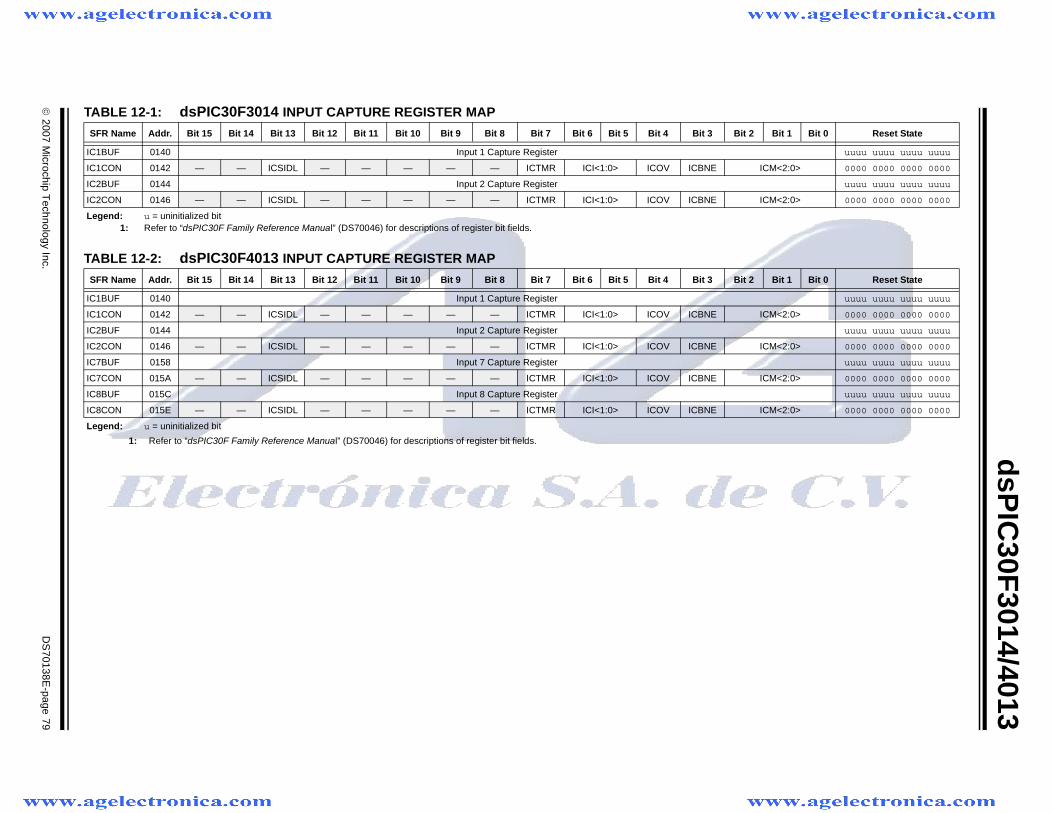
© 2007 M
icrochip Technology Inc.
DS
70138E-page 79
dsP
IC30F
3014/4013
TABLE 12-1: dsPIC30F3014 INPUT CAPTURE REGISTER MAP
TABLE 12-2: dsPIC30F4013 INPUT CAPTURE REGISTER MAP
SFR Name Addr. Bit 15 Bit 14 Bit 13 Bit 12 Bit 11 Bit 10 Bit 9 Bit 8 Bit 7 Bit 6 Bit 5 Bit 4 Bit 3 Bit 2 Bit 1 Bit 0 Reset State
IC1BUF 0140 Input 1 Capture Register uuuu uuuu uuuu uuuu
IC1CON 0142 — — ICSIDL — — — — — ICTMR ICI<1:0> ICOV ICBNE ICM<2:0> 0000 0000 0000 0000
IC2BUF 0144 Input 2 Capture Register uuuu uuuu uuuu uuuu
IC2CON 0146 — — ICSIDL — — — — — ICTMR ICI<1:0> ICOV ICBNE ICM<2:0> 0000 0000 0000 0000
Legend: u = uninitialized bit1: Refer to “dsPIC30F Family Reference Manual” (DS70046) for descriptions of register bit fields.
SFR Name Addr. Bit 15 Bit 14 Bit 13 Bit 12 Bit 11 Bit 10 Bit 9 Bit 8 Bit 7 Bit 6 Bit 5 Bit 4 Bit 3 Bit 2 Bit 1 Bit 0 Reset State
IC1BUF 0140 Input 1 Capture Register uuuu uuuu uuuu uuuu
IC1CON 0142 — — ICSIDL — — — — — ICTMR ICI<1:0> ICOV ICBNE ICM<2:0> 0000 0000 0000 0000
IC2BUF 0144 Input 2 Capture Register uuuu uuuu uuuu uuuu
IC2CON 0146 — — ICSIDL — — — — — ICTMR ICI<1:0> ICOV ICBNE ICM<2:0> 0000 0000 0000 0000
IC7BUF 0158 Input 7 Capture Register uuuu uuuu uuuu uuuu
IC7CON 015A — — ICSIDL — — — — — ICTMR ICI<1:0> ICOV ICBNE ICM<2:0> 0000 0000 0000 0000
IC8BUF 015C Input 8 Capture Register uuuu uuuu uuuu uuuu
IC8CON 015E — — ICSIDL — — — — — ICTMR ICI<1:0> ICOV ICBNE ICM<2:0> 0000 0000 0000 0000
Legend: u = uninitialized bit
1: Refer to “dsPIC30F Family Reference Manual” (DS70046) for descriptions of register bit fields.

dsPIC30F3014/4013
DS70138E-page 80 © 2007 Microchip Technology Inc.
NOTES:
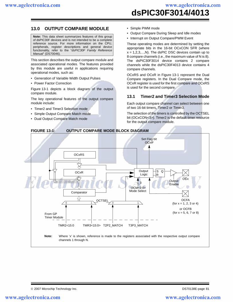
© 2007 Microchip Technology Inc. DS70138E-page 81
dsPIC30F3014/4013
13.0 OUTPUT COMPARE MODULE
This section describes the output compare module andassociated operational modes. The features providedby this module are useful in applications requiringoperational modes, such as:
• Generation of Variable Width Output Pulses• Power Factor Correction
Figure 13-1 depicts a block diagram of the outputcompare module.
The key operational features of the output comparemodule include:
• Timer2 and Timer3 Selection mode
• Simple Output Compare Match mode• Dual Output Compare Match mode
• Simple PWM mode• Output Compare During Sleep and Idle modes
• Interrupt on Output Compare/PWM Event
These operating modes are determined by setting theappropriate bits in the 16-bit OCxCON SFR (wherex = 1,2,3,...,N). The dsPIC DSC devices contain up to8 compare channels (i.e., the maximum value of N is 8).The dsPIC30F3014 device contains 2 comparechannels while the dsPIC30F4013 device contains 4compare channels.
OCxRS and OCxR in Figure 13-1 represent the DualCompare registers. In the Dual Compare mode, theOCxR register is used for the first compare and OCxRSis used for the second compare.
13.1 Timer2 and Timer3 Selection Mode
Each output compare channel can select between oneof two 16-bit timers, Timer2 or Timer3.
The selection of the timers is controlled by the OCTSELbit (OCxCON<3>). Timer2 is the default timer resourcefor the output compare module.
FIGURE 13-1: OUTPUT COMPARE MODE BLOCK DIAGRAM
Note: This data sheet summarizes features of this groupof dsPIC30F devices and is not intended to be a completereference source. For more information on the CPU,peripherals, register descriptions and general devicefunctionality, refer to the “dsPIC30F Family ReferenceManual” (DS70046).
OCxR
Comparator
OutputLogic
QSR
OCM<2:0>
OutputOCx
Set Flag bitOCxIF
OCxRS
Mode Select
3
Note: Where ‘x’ is shown, reference is made to the registers associated with the respective output comparechannels 1 through N.
OCFA OCTSEL
0 1
T2P2_MATCHTMR2<15:0 TMR3<15:0> T3P3_MATCH
From GP
(for x = 1, 2, 3 or 4)
or OCFB(for x = 5, 6, 7 or 8)
0 1
Timer Module
Enable
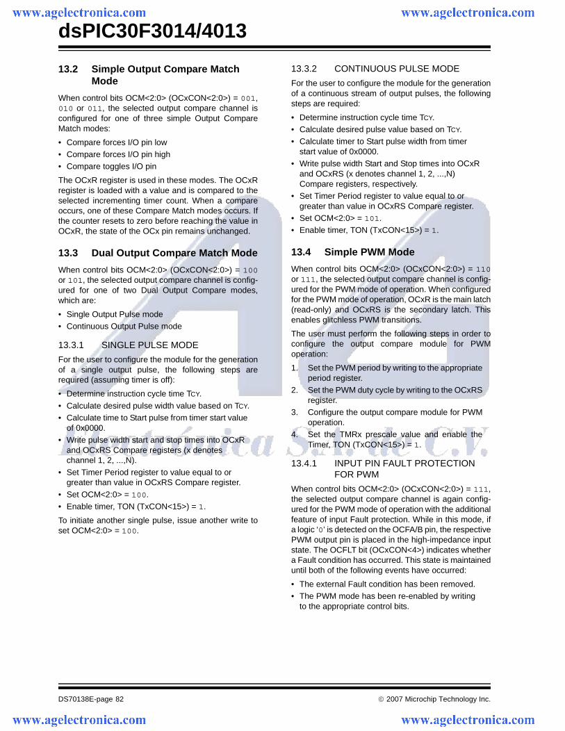
dsPIC30F3014/4013
DS70138E-page 82 © 2007 Microchip Technology Inc.
13.2 Simple Output Compare Match Mode
When control bits OCM<2:0> (OCxCON<2:0>) = 001,010 or 011, the selected output compare channel isconfigured for one of three simple Output CompareMatch modes:
• Compare forces I/O pin low• Compare forces I/O pin high• Compare toggles I/O pin
The OCxR register is used in these modes. The OCxRregister is loaded with a value and is compared to theselected incrementing timer count. When a compareoccurs, one of these Compare Match modes occurs. Ifthe counter resets to zero before reaching the value inOCxR, the state of the OCx pin remains unchanged.
13.3 Dual Output Compare Match Mode
When control bits OCM<2:0> (OCxCON<2:0>) = 100or 101, the selected output compare channel is config-ured for one of two Dual Output Compare modes,which are:
• Single Output Pulse mode• Continuous Output Pulse mode
13.3.1 SINGLE PULSE MODE
For the user to configure the module for the generationof a single output pulse, the following steps arerequired (assuming timer is off):
• Determine instruction cycle time TCY.
• Calculate desired pulse width value based on TCY.• Calculate time to Start pulse from timer start value
of 0x0000.• Write pulse width start and stop times into OCxR
and OCxRS Compare registers (x denotes channel 1, 2, ...,N).
• Set Timer Period register to value equal to or greater than value in OCxRS Compare register.
• Set OCM<2:0> = 100.• Enable timer, TON (TxCON<15>) = 1.
To initiate another single pulse, issue another write toset OCM<2:0> = 100.
13.3.2 CONTINUOUS PULSE MODE
For the user to configure the module for the generationof a continuous stream of output pulses, the followingsteps are required:
• Determine instruction cycle time TCY.• Calculate desired pulse value based on TCY.• Calculate timer to Start pulse width from timer
start value of 0x0000.• Write pulse width Start and Stop times into OCxR
and OCxRS (x denotes channel 1, 2, ...,N) Compare registers, respectively.
• Set Timer Period register to value equal to or greater than value in OCxRS Compare register.
• Set OCM<2:0> = 101.• Enable timer, TON (TxCON<15>) = 1.
13.4 Simple PWM Mode
When control bits OCM<2:0> (OCxCON<2:0>) = 110or 111, the selected output compare channel is config-ured for the PWM mode of operation. When configuredfor the PWM mode of operation, OCxR is the main latch(read-only) and OCxRS is the secondary latch. Thisenables glitchless PWM transitions.
The user must perform the following steps in order toconfigure the output compare module for PWMoperation:
1. Set the PWM period by writing to the appropriateperiod register.
2. Set the PWM duty cycle by writing to the OCxRSregister.
3. Configure the output compare module for PWMoperation.
4. Set the TMRx prescale value and enable theTimer, TON (TxCON<15>) = 1.
13.4.1 INPUT PIN FAULT PROTECTION FOR PWM
When control bits OCM<2:0> (OCxCON<2:0>) = 111,the selected output compare channel is again config-ured for the PWM mode of operation with the additionalfeature of input Fault protection. While in this mode, ifa logic ‘0’ is detected on the OCFA/B pin, the respectivePWM output pin is placed in the high-impedance inputstate. The OCFLT bit (OCxCON<4>) indicates whethera Fault condition has occurred. This state is maintaineduntil both of the following events have occurred:
• The external Fault condition has been removed. • The PWM mode has been re-enabled by writing
to the appropriate control bits.
© 2007 Microchip Technology Inc. DS70138E-page 83
dsPIC30F3014/4013
13.4.2 PWM PERIOD
The PWM period is specified by writing to the PRxregister. The PWM period can be calculated usingEquation 13-1.
EQUATION 13-1:
PWM frequency is defined as 1/[PWM period].
When the selected TMRx is equal to its respectiveperiod register, PRx, the following four events occur onthe next increment cycle:
• TMRx is cleared.
• The OCx pin is set. - Exception 1: If PWM duty cycle is 0x0000,
the OCx pin remains low.- Exception 2: If duty cycle is greater than PRx,
the pin remains high.• The PWM duty cycle is latched from OCxRS into
OCxR.• The corresponding timer interrupt flag is set.
See Figure 13-2 for key PWM period comparisons.Timer3 is referred to in Figure 13-2 for clarity.
FIGURE 13-2: PWM OUTPUT TIMING
13.5 Output Compare Operation During CPU Sleep Mode
When the CPU enters Sleep mode, all internal clocksare stopped. Therefore, when the CPU enters theSleep state, the output compare channel drives the pinto the active state that was observed prior to enteringthe CPU Sleep state.
For example, if the pin was high when the CPU enteredthe Sleep state, the pin remains high. Likewise, if thepin was low when the CPU entered the Sleep state, thepin remains low. In either case, the output comparemodule resumes operation when the device wakes up.
13.6 Output Compare Operation During CPU Idle Mode
When the CPU enters the Idle mode, the outputcompare module can operate with full functionality.
The output compare channel operates during the CPUIdle mode if the OCSIDL bit (OCxCON<13>) is at logic‘0’ and the selected time base (Timer2 or Timer3) isenabled and the TSIDL bit of the selected timer is setto logic ‘0’.
13.7 Output Compare Interrupts
The output compare channels have the ability to gener-ate an interrupt on a compare match, for whicheverMatch mode has been selected.
For all modes, except the PWM mode, when a com-pare event occurs, the respective interrupt flag (OCxIF)is asserted and an interrupt is generated, if enabled.The OCxIF bit is located in the corresponding IFSSTATUS register and must be cleared in software. Theinterrupt is enabled via the respective compare inter-rupt enable (OCxIE) bit located in the correspondingIEC Control register.
For the PWM mode, when an event occurs, the respec-tive timer interrupt flag (T2IF or T3IF) is asserted andan interrupt is generated, if enabled. The IF bit islocated in the IFS0 STATUS register and must becleared in software. The interrupt is enabled via therespective timer interrupt enable bit (T2IE or T3IE)located in the IEC0 Control register. The outputcompare interrupt flag is never set during the PWMmode of operation.
PWM period = [(PRx) + 1] • 4 • TOSC •(TMRx prescale value)
Period
Duty Cycle
TMR3 = Duty Cycle TMR3 = Duty Cycle
TMR3 = PR3T3IF = 1
(Interrupt Flag)OCxR = OCxRS
TMR3 = PR3
(Interrupt Flag)OCxR = OCxRS
T3IF = 1
(OCxR) (OCxR)
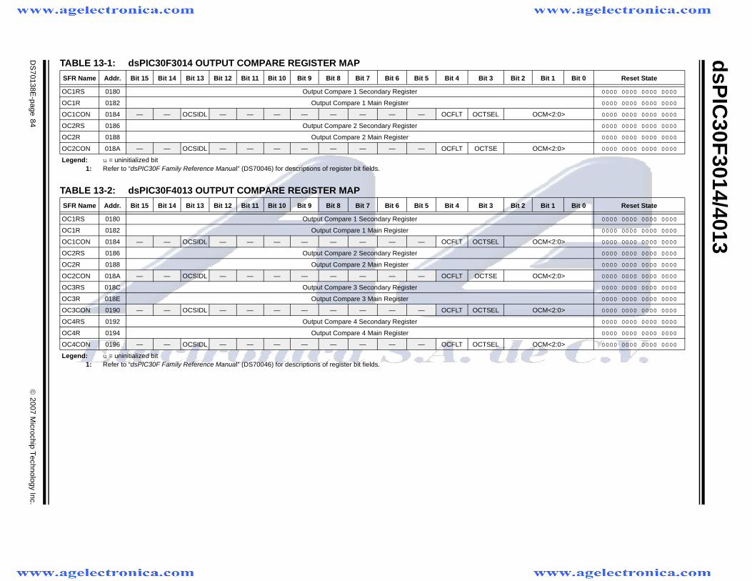
dsP
IC30F
3014/4013
DS
70138E-page 84
© 2007 M
icrochip Technology Inc.
TABLE 13-1: dsPIC30F3014 OUTPUT COMPARE REGISTER MAP
TABLE 13-2: dsPIC30F4013 OUTPUT COMPARE REGISTER MAP
SFR Name Addr. Bit 15 Bit 14 Bit 13 Bit 12 Bit 11 Bit 10 Bit 9 Bit 8 Bit 7 Bit 6 Bit 5 Bit 4 Bit 3 Bit 2 Bit 1 Bit 0 Reset State
OC1RS 0180 Output Compare 1 Secondary Register 0000 0000 0000 0000
OC1R 0182 Output Compare 1 Main Register 0000 0000 0000 0000
OC1CON 0184 — — OCSIDL — — — — — — — — OCFLT OCTSEL OCM<2:0> 0000 0000 0000 0000
OC2RS 0186 Output Compare 2 Secondary Register 0000 0000 0000 0000
OC2R 0188 Output Compare 2 Main Register 0000 0000 0000 0000
OC2CON 018A — — OCSIDL — — — — — — — — OCFLT OCTSE OCM<2:0> 0000 0000 0000 0000
Legend: u = uninitialized bit1: Refer to “dsPIC30F Family Reference Manual” (DS70046) for descriptions of register bit fields.
SFR Name Addr. Bit 15 Bit 14 Bit 13 Bit 12 Bit 11 Bit 10 Bit 9 Bit 8 Bit 7 Bit 6 Bit 5 Bit 4 Bit 3 Bit 2 Bit 1 Bit 0 Reset State
OC1RS 0180 Output Compare 1 Secondary Register 0000 0000 0000 0000
OC1R 0182 Output Compare 1 Main Register 0000 0000 0000 0000
OC1CON 0184 — — OCSIDL — — — — — — — — OCFLT OCTSEL OCM<2:0> 0000 0000 0000 0000
OC2RS 0186 Output Compare 2 Secondary Register 0000 0000 0000 0000
OC2R 0188 Output Compare 2 Main Register 0000 0000 0000 0000
OC2CON 018A — — OCSIDL — — — — — — — — OCFLT OCTSE OCM<2:0> 0000 0000 0000 0000
OC3RS 018C Output Compare 3 Secondary Register 0000 0000 0000 0000
OC3R 018E Output Compare 3 Main Register 0000 0000 0000 0000
OC3CON 0190 — — OCSIDL — — — — — — — — OCFLT OCTSEL OCM<2:0> 0000 0000 0000 0000
OC4RS 0192 Output Compare 4 Secondary Register 0000 0000 0000 0000
OC4R 0194 Output Compare 4 Main Register 0000 0000 0000 0000
OC4CON 0196 — — OCSIDL — — — — — — — — OCFLT OCTSEL OCM<2:0> 0000 0000 0000 0000
Legend: u = uninitialized bit1: Refer to “dsPIC30F Family Reference Manual” (DS70046) for descriptions of register bit fields.
© 2007 Microchip Technology Inc. DS70138E-page 85
dsPIC30F3014/4013
14.0 I2C MODULE
The Inter-Integrated Circuit (I2CTM) module providescomplete hardware support for both Slave and Multi-Master modes of the I2C serial communicationstandard, with a 16-bit interface.
This module offers the following key features:
• I2C interface supporting both master and slave operation.
• I2C Slave mode supports 7 and 10-bit address.• I2C Master mode supports 7 and 10-bit address.• I2C port allows bidirectional transfers between
master and slaves.• Serial clock synchronization for I2C port can be
used as a handshake mechanism to suspend and resume serial transfer (SCLREL control).
• I2C supports multi-master operation; detects bus collision and arbitrates accordingly.
14.1 Operating Function Description
The hardware fully implements all the master and slavefunctions of the I2C Standard and Fast modespecifications, as well as 7 and 10-bit addressing.
Thus, the I2C module can operate either as a slave ora master on an I2C bus.
14.1.1 VARIOUS I2C MODES
The following types of I2C operation are supported:
• I2C slave operation with 7-bit address
• I2C slave operation with 10-bit address• I2C master operation with 7 or 10-bit address
See the I2C programmer’s model in Figure 14-1.
14.1.2 PIN CONFIGURATION IN I2C MODE
I2C has a 2-pin interface: the SCL pin is clock and theSDA pin is data.
14.1.3 I2C REGISTERS
I2CCON and I2CSTAT are control and STATUS regis-ters, respectively. The I2CCON register is readable andwritable. The lower 6 bits of I2CSTAT are read-only.The remaining bits of the I2CSTAT are read/write.
I2CRSR is the shift register used for shifting data,whereas I2CRCV is the buffer register to which databytes are written, or from which data bytes are read.I2CRCV is the receive buffer as shown in Figure 14-1.I2CTRN is the transmit register to which bytes arewritten during a transmit operation, as shown inFigure 14-2.
The I2CADD register holds the slave address. A Statusbit, ADD10, indicates 10-bit Address mode. TheI2CBRG acts as the Baud Rate Generator reloadvalue.
In receive operations, I2CRSR and I2CRCV togetherform a double-buffered receiver. When I2CRSRreceives a complete byte, it is transferred to I2CRCVand an interrupt pulse is generated. Duringtransmission, the I2CTRN is not double-buffered.
FIGURE 14-1: PROGRAMMER’S MODEL
Note: This data sheet summarizes features of this groupof dsPIC30F devices and is not intended to be a completereference source. For more information on the CPU,peripherals, register descriptions and general devicefunctionality, refer to the 'dsPIC30F Family ReferenceManual' (DS70046).
Note: Following a Restart condition in 10-bitmode, the user only needs to match thefirst 7-bit address.
Bit 7 Bit 0I2CRCV (8 bits)
Bit 7 Bit 0I2CTRN (8 bits)
Bit 8 Bit 0I2CBRG (9 bits)
Bit 15 Bit 0I2CCON (16 bits)
Bit 15 Bit 0I2CSTAT (16 bits)
Bit 9 Bit 0I2CADD (10 bits)
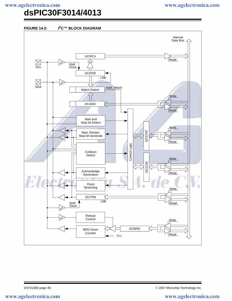
dsPIC30F3014/4013
DS70138E-page 86 © 2007 Microchip Technology Inc.
FIGURE 14-2: I2C™ BLOCK DIAGRAM
I2CRSR
I2CRCV
InternalData Bus
SCL
SDA
Shift
Match Detect
I2CADD
Start andStop bit Detect
Clock
Addr_Match
ClockStretching
I2CTRNLSBShift
Clock
Write
Read
BRG Down I2CBRG
ReloadControl
FCY
Start, Restart,Stop bit Generate
Write
Read
AcknowledgeGeneration
CollisionDetect
Write
Read
Write
ReadI2C
CO
N
Write
ReadI2C
STA
T
Con
trol
Log
ic
Read
LSB
Counter
© 2007 Microchip Technology Inc. DS70138E-page 87
dsPIC30F3014/4013
14.2 I2C Module Addresses
The I2CADD register contains the Slave modeaddresses. The register is a 10-bit register.
If the A10M bit (I2CCON<10>) is ‘0’, the address isinterpreted by the module as a 7-bit address. When anaddress is received, it is compared to the 7 LSbs of theI2CADD register.
If the A10M bit is ‘1’, the address is assumed to be a10-bit address. When an address is received, it is com-pared with the binary value, ‘11110 A9 A8’ (where A9and A8 are two Most Significant bits of I2CADD). If thatvalue matches, the next address is compared with theLeast Significant 8 bits of I2CADD, as specified in the10-bit addressing protocol.
14.3 I2C 7-bit Slave Mode Operation
Once enabled (I2CEN = 1), the slave module waits fora Start bit to occur (i.e., the I2C module is ‘Idle’). Follow-ing the detection of a Start bit, 8 bits are shifted intoI2CRSR, and the address is compared againstI2CADD. In 7-bit mode (A10M = 0), bits I2CADD<6:0>are compared against I2CRSR<7:1> and I2CRSR<0>is the R_W bit. All incoming bits are sampled on therising edge of SCL.
If an address match occurs, an acknowledgement issent and the slave event interrupt flag (SI2CIF) is seton the falling edge of the ninth (ACK) bit. The addressmatch does not affect the contents of the I2CRCVbuffer or the RBF bit.
14.3.1 SLAVE TRANSMISSION
If the R_W bit received is a ‘1’, the serial port goes intoTransmit mode. It sends ACK on the ninth bit and thenholds SCL to ‘0’ until the CPU responds by writing toI2CTRN. SCL is released by setting the SCLREL bit,and 8 bits of data are shifted out. Data bits are shiftedout on the falling edge of SCL, such that SDA is validduring SCL high. The interrupt pulse is sent on thefalling edge of the ninth clock pulse, regardless of thestatus of the ACK received from the master.
14.3.2 SLAVE RECEPTION
If the R_W bit received is a ‘0’ during an addressmatch, then Receive mode is initiated. Incoming bitsare sampled on the rising edge of SCL. After 8 bits arereceived, if I2CRCV is not full or I2COV is not set,I2CRSR is transferred to I2CRCV. ACK is sent on theninth clock.
If the RBF flag is set, indicating that I2CRCV is stillholding data from a previous operation (RBF = 1), thenACK is not sent; however, the interrupt pulse is gener-ated. In the case of an overflow, the contents of theI2CRSR are not loaded into the I2CRCV.
14.4 I2C 10-bit Slave Mode Operation
In 10-bit mode, the basic receive and transmit opera-tions are the same as in the 7-bit mode. However, thecriteria for address match is more complex.
The I2C specification dictates that a slave must beaddressed for a write operation with two address bytesfollowing a Start bit.
The A10M bit is a control bit that signifies that theaddress in I2CADD is a 10-bit address rather than a 7-bitaddress. The address detection protocol for the first byteof a message address is identical for 7-bit and 10-bitmessages, but the bits being compared are different.
I2CADD holds the entire 10-bit address. Upon receiv-ing an address following a Start bit, I2CRSR <7:3> iscompared against a literal ‘11110’ (the default 10-bitaddress) and I2CRSR<2:1> are compared againstI2CADD<9:8>. If a match occurs and if R_W = 0, theinterrupt pulse is sent. The ADD10 bit is cleared to indi-cate a partial address match. If a match fails or R_W =1, the ADD10 bit is cleared and the module returns tothe Idle state.
The low byte of the address is then received and com-pared with I2CADD<7:0>. If an address match occurs,the interrupt pulse is generated and the ADD10 bit isset, indicating a complete 10-bit address match. If anaddress match did not occur, the ADD10 bit is clearedand the module returns to the Idle state.
14.4.1 10-BIT MODE SLAVE TRANSMISSION
Once a slave is addressed in this fashion with the full10-bit address (we refer to this state as“PRIOR_ADDR_MATCH”), the master can beginsending data bytes for a slave reception operation.
TABLE 14-1: 7-BIT I2C™ SLAVE ADDRESSES SUPPORTED BY dsPIC30F
0x00 General call address or start byte
0x01-0x03 Reserved
0x04-0x07 Hs-mode Master codes
0x08-0x77 Valid 7-bit addresses
0x78-0x7b Valid 10-bit addresses (lower 7 bits)
0x7c-0x7f Reserved
Note: The I2CRCV is loaded if the I2COV bit = 1and the RBF flag = 0. In this case, a readof the I2CRCV was performed but the userdid not clear the state of the I2COV bitbefore the next receive occurred. Theacknowledgement is not sent (ACK = 1)and the I2CRCV is updated.
dsPIC30F3014/4013
DS70138E-page 88 © 2007 Microchip Technology Inc.
14.4.2 10-BIT MODE SLAVE RECEPTION
Once addressed, the master can generate a RepeatedStart, reset the high byte of the address and set theR_W bit without generating a Stop bit, thus initiating aslave transmit operation.
14.5 Automatic Clock Stretch
In the Slave modes, the module can synchronize bufferreads and write to the master device by clock stretching.
14.5.1 TRANSMIT CLOCK STRETCHING
Both 10-bit and 7-bit Transmit modes implement clockstretching by asserting the SCLREL bit after the fallingedge of the ninth clock, if the TBF bit is cleared,indicating the buffer is empty.
In Slave Transmit modes, clock stretching is alwaysperformed irrespective of the STREN bit.
Clock synchronization takes place following the ninthclock of the transmit sequence. If the device samplesan ACK on the falling edge of the ninth clock and if theTBF bit is still clear, then the SCLREL bit is automati-cally cleared. The SCLREL being cleared to ‘0’ assertsthe SCL line low. The user’s ISR must set the SCLRELbit before transmission is allowed to continue. By hold-ing the SCL line low, the user has time to service theISR and load the contents of the I2CTRN before themaster device can initiate another transmit sequence.
14.5.2 RECEIVE CLOCK STRETCHING
The STREN bit in the I2CCON register can be used toenable clock stretching in Slave Receive mode. Whenthe STREN bit is set, the SCL pin is held low at the endof each data receive sequence.
14.5.3 CLOCK STRETCHING DURING 7-BIT ADDRESSING (STREN = 1)
When the STREN bit is set in Slave Receive mode, theSCL line is held low when the buffer register is full. Themethod for stretching the SCL output is the same forboth 7 and 10-bit addressing modes.
Clock stretching takes place following the ninth clock ofthe receive sequence. On the falling edge of the ninthclock at the end of the ACK sequence, if the RBF bit isset, the SCLREL bit is automatically cleared, forcingthe SCL output to be held low. The user’s ISR must setthe SCLREL bit before reception is allowed to continue.By holding the SCL line low, the user has time to ser-vice the ISR and read the contents of the I2CRCVbefore the master device can initiate another receivesequence. This prevents buffer overruns fromoccurring.
14.5.4 CLOCK STRETCHING DURING 10-BIT ADDRESSING (STREN = 1)
Clock stretching takes place automatically during theaddressing sequence. Because this module has aregister for the entire address, it is not necessary forthe protocol to wait for the address to be updated.
After the address phase is complete, clock stretchingoccurs on each data receive or transmit sequence, asdescribed earlier.
14.6 Software Controlled Clock Stretching (STREN = 1)
When the STREN bit is ‘1’, the SCLREL bit can becleared by software to allow software to control theclock stretching. Program logic synchronizes writes tothe SCLREL bit with the SCL clock. Clearing theSCLREL bit does not assert the SCL output until themodule detects a falling edge on the SCL output andSCL is sampled low. If the SCLREL bit is cleared by theuser while the SCL line has been sampled low, the SCLoutput is asserted (held low). The SCL output remainslow until the SCLREL bit is set and all other devices onthe I2C bus have de-asserted SCL. This ensures that awrite to the SCLREL bit does not violate the minimumhigh time requirement for SCL.
If the STREN bit is ‘0’, a software write to the SCLRELbit is disregarded and has no effect on the SCLREL bit.
Note 1: If the user loads the contents of I2CTRN,setting the TBF bit before the falling edgeof the ninth clock, the SCLREL bit is notbe cleared and clock stretching does notoccur.
2: The SCLREL bit can be set in software,regardless of the state of the TBF bit.
Note 1: If the user reads the contents of theI2CRCV, clearing the RBF bit before thefalling edge of the ninth clock, theSCLREL bit is not cleared and clockstretching does not occur.
2: The SCLREL bit can be set in softwareregardless of the state of the RBF bit. Theuser should be careful to clear the RBF bitin the ISR before the next receivesequence in order to prevent an overflowcondition.
© 2007 Microchip Technology Inc. DS70138E-page 89
dsPIC30F3014/4013
14.7 Interrupts
The I2C module generates two interrupt flags, MI2CIF(I2C Master Interrupt Flag) and SI2CIF (I2C Slave Inter-rupt Flag). The MI2CIF interrupt flag is activated oncompletion of a master message event. The SI2CIFinterrupt flag is activated on detection of a messagedirected to the slave.
14.8 Slope Control
The I2C standard requires slope control on the SDAand SCL signals for Fast mode (400 kHz). The controlbit, DISSLW, enables the user to disable slew ratecontrol if desired. It is necessary to disable the slewrate control for 1 MHz mode.
14.9 IPMI Support
The control bit, IPMIEN, enables the module to supportIntelligent Peripheral Management Interface (IPMI).When this bit is set, the module accepts and acts uponall addresses.
14.10 General Call Address Support
The general call address can address all devices.When this address is used, all devices should, intheory, respond with an acknowledgement.
The general call address is one of eight addressesreserved for specific purposes by the I2C protocol. Itconsists of all ‘0’s with R_W = 0.
The general call address is recognized when the Gen-eral Call Enable (GCEN) bit is set (I2CCON<7> = 1).Following a Start bit detection, 8 bits are shifted intoI2CRSR and the address is compared with I2CADD,and is also compared with the general call addresswhich is fixed in hardware.
If a general call address match occurs, the I2CRSR istransferred to the I2CRCV after the eighth clock, theRBF flag is set and on the falling edge of the ninth bit(ACK bit), the master event interrupt flag (MI2CIF) isset.
When the interrupt is serviced, the source for theinterrupt can be checked by reading the contents of theI2CRCV to determine if the address was device-spe-cific or a general call address.
14.11 I2C Master Support
As a master device, six operations are supported:
• Assert a Start condition on SDA and SCL.
• Assert a Restart condition on SDA and SCL.• Write to the I2CTRN register initiating
transmission of data/address.• Generate a Stop condition on SDA and SCL.• Configure the I2C port to receive data.
• Generate an ACK condition at the end of a received byte of data.
14.12 I2C Master Operation
The master device generates all of the serial clockpulses and the Start and Stop conditions. A transfer isended with a Stop condition or with a Repeated Startcondition. Since the Repeated Start condition is alsothe beginning of the next serial transfer, the I2C bus isnot released.
In Master Transmitter mode, serial data is outputthrough SDA, while SCL outputs the serial clock. Thefirst byte transmitted contains the slave address of thereceiving device (7 bits) and the data direction bit. Inthis case, the data direction bit (R_W) is logic ‘0’. Serialdata is transmitted 8 bits at a time. After each byte istransmitted, an ACK bit is received. Start and Stopconditions are output to indicate the beginning and theend of a serial transfer.
In Master Receive mode, the first byte transmittedcontains the slave address of the transmitting device(7 bits) and the data direction bit. In this case, the datadirection bit (R_W) is logic ‘1’. Thus, the first byte trans-mitted is a 7-bit slave address, followed by a ‘1’ to indi-cate receive bit. Serial data is received via SDA whileSCL outputs the serial clock. Serial data is received8 bits at a time. After each byte is received, an ACK bitis transmitted. Start and Stop conditions indicate thebeginning and end of transmission.
14.12.1 I2C MASTER TRANSMISSION
Transmission of a data byte, a 7-bit address or thesecond half of a 10-bit address, is accomplished bysimply writing a value to I2CTRN register. The usershould only write to I2CTRN when the module is in aWAIT state. This action sets the Buffer Full Flag (TBF)and allow the Baud Rate Generator to begin countingand start the next transmission. Each bit of address/data is shifted out onto the SDA pin after the fallingedge of SCL is asserted. The Transmit Status Flag,TRSTAT (I2CSTAT<14>), indicates that a mastertransmit is in progress.
dsPIC30F3014/4013
DS70138E-page 90 © 2007 Microchip Technology Inc.
14.12.2 I2C MASTER RECEPTION
Master mode reception is enabled by programming theReceive Enable bit, RCEN (I2CCON<3>). The I2Cmodule must be Idle before the RCEN bit is set, other-wise the RCEN bit is disregarded. The Baud Rate Gen-erator begins counting and on each rollover, the stateof the SCL pin ACK and data are shifted into theI2CRSR on the rising edge of each clock.
14.12.3 BAUD RATE GENERATOR
In I2C Master mode, the reload value for the BRG islocated in the I2CBRG register. When the BRG isloaded with this value, the BRG counts down to ‘0’ andstops until another reload has taken place. If clockarbitration is taking place, for instance, the BRG isreloaded when the SCL pin is sampled high.
As per the I2C standard, FSCK may be 100 kHz or400 kHz. However, the user can specify any baud rateup to 1 MHz. I2CBRG values of ‘0’ or ‘1’ are illegal.
EQUATION 14-1: SERIAL CLOCK RATE
14.12.4 CLOCK ARBITRATION
Clock arbitration occurs when the master de-assertsthe SCL pin (SCL allowed to float high) during anyreceive, transmit, or Restart/Stop condition. When theSCL pin is allowed to float high, the Baud Rate Gener-ator (BRG) is suspended from counting until the SCLpin is actually sampled high. When the SCL pin is sam-pled high, the Baud Rate Generator is reloaded withthe contents of I2CBRG and begins counting. Thisensures that the SCL high time is always at least oneBRG rollover count in the event that the clock is heldlow by an external device.
14.12.5 MULTI-MASTER COMMUNICATION, BUS COLLISION AND BUS ARBITRATION
Multi-master operation support is achieved by bus arbi-tration. When the master outputs address/data bitsonto the SDA pin, arbitration takes place when themaster outputs a ‘1’ on SDA by letting SDA float highwhile another master asserts a ‘0’. When the SCL pinfloats high, data should be stable. If the expected dataon SDA is a ‘1’ and the data sampled on the SDApin = 0, then a bus collision has taken place. Themaster sets the MI2CIF pulse and resetS the masterportion of the I2C port to its Idle state.
If a transmit was in progress when the bus collisionoccurred, the transmission is halted, the TBF flag iscleared, the SDA and SCL lines are de-asserted and avalue can now be written to I2CTRN. When the userservices the I2C master event Interrupt Service Rou-tine, if the I2C bus is free (i.e., the P bit is set), the usercan resume communication by asserting a Startcondition.
If a Start, Restart, Stop or Acknowledge condition wasin progress when the bus collision occurred, the condi-tion is aborted, the SDA and SCL lines are de-asserted,and the respective control bits in the I2CCON registerare cleared to ‘0’. When the user services the buscollision Interrupt Service Routine, and if the I2C bus isfree, the user can resume communication by assertinga Start condition.
The master continues to monitor the SDA and SCLpins, and if a Stop condition occurs, the MI2CIF bit isset.
A write to the I2CTRN starts the transmission of data atthe first data bit, regardless of where the transmitter leftoff when bus collision occurred.
In a multi-master environment, the interrupt generationon the detection of Start and Stop conditions allows thedetermination of when the bus is free. Control of the I2Cbus can be taken when the P bit is set in the I2CSTATregister, or the bus is Idle and the S and P bits arecleared.
14.13 I2C Module Operation During CPU Sleep and Idle Modes
14.13.1 I2C OPERATION DURING CPU SLEEP MODE
When the device enters Sleep mode, all clock sourcesto the module are shut down and stay at logic ‘0’. IfSleep occurs in the middle of a transmission and thestate machine is partially into a transmission as theclocks stop, then the transmission is aborted. Similarly,if Sleep occurs in the middle of a reception, then thereception is aborted.
14.13.2 I2C OPERATION DURING CPU IDLE MODE
For the I2C, the I2CSIDL bit determines if the modulestops or continues on Idle. If I2CSIDL = 0, the modulecontinues operation on assertion of the Idle mode. IfI2CSIDL = 1, the module stops on Idle.
I2CBRG = FCY FCYFSCK 1,111,111
– 1–( )
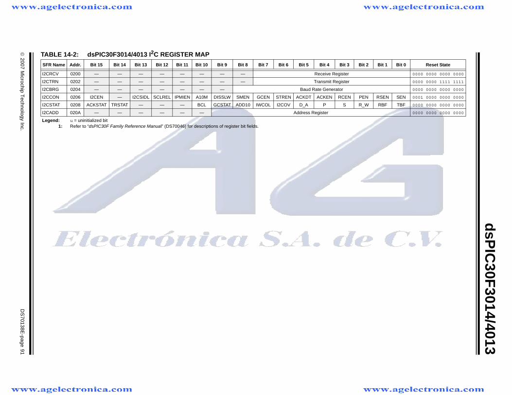
© 2007 M
icrochip Technology Inc.
DS
70138E-page 91
dsP
IC30F
3014/4013
TABLE 14-2: dsPIC30F3014/4013 I2C REGISTER MAP
SFR Name Addr. Bit 15 Bit 14 Bit 13 Bit 12 Bit 11 Bit 10 Bit 9 Bit 8 Bit 7 Bit 6 Bit 5 Bit 4 Bit 3 Bit 2 Bit 1 Bit 0 Reset State
I2CRCV 0200 — — — — — — — — Receive Register 0000 0000 0000 0000
I2CTRN 0202 — — — — — — — — Transmit Register 0000 0000 1111 1111
I2CBRG 0204 — — — — — — — Baud Rate Generator 0000 0000 0000 0000
I2CCON 0206 I2CEN — I2CSIDL SCLREL IPMIEN A10M DISSLW SMEN GCEN STREN ACKDT ACKEN RCEN PEN RSEN SEN 0001 0000 0000 0000
I2CSTAT 0208 ACKSTAT TRSTAT — — — BCL GCSTAT ADD10 IWCOL I2COV D_A P S R_W RBF TBF 0000 0000 0000 0000
I2CADD 020A — — — — — — Address Register 0000 0000 0000 0000
Legend: u = uninitialized bit1: Refer to “dsPIC30F Family Reference Manual” (DS70046) for descriptions of register bit fields.

dsPIC30F3014/4013
DS70138E-page 92 © 2007 Microchip Technology Inc.
NOTES:
© 2007 Microchip Technology Inc. DS70138E-page 93
dsPIC30F3014/4013
15.0 SPI MODULE
The Serial Peripheral Interface (SPI) module is a syn-chronous serial interface. It is useful for communicatingwith other peripheral devices, such as EEPROMs, shiftregisters, display drivers and A/D converters, or othermicrocontrollers. It is compatible with Motorola’s SPIand SIOP interfaces. The dsPIC30F3014 anddsPIC30F4013 devices feature one SPI module, SPI1.
15.1 Operating Function Description
Each SPI module consists of a 16-bit shift register,SPIxSR (where x = 1 or 2) , used for shifting data in andout, and a buffer register, SPIxBUF. A control register,SPIxCON, configures the module. Additionally, aSTATUS register, SPIxSTAT, indicates various statusconditions.
The serial interface consists of 4 pins: SDIx (serial datainput), SDOx (serial data output), SCKx (shift clockinput or output), and SSx (active-low slave select).
In Master mode operation, SCK is a clock output but inSlave mode, it is a clock input.
A series of eight (8) or sixteen (16) clock pulses shiftout bits from the SPIxSR to SDOx pin and simulta-neously shift in data from SDIx pin. An interrupt is gen-erated when the transfer is complete and thecorresponding interrupt flag bit (SPI1IF or SPI2IF) isset. This interrupt can be disabled through an interruptenable bit (SPI1IE or SPI2IE).
The receive operation is double-buffered. When a com-plete byte is received, it is transferred from SPIxSR toSPIxBUF.
If the receive buffer is full when new data is being trans-ferred from SPIxSR to SPIxBUF, the module sets theSPIROV bit, indicating an overflow condition. Thetransfer of the data from SPIxSR to SPIxBUF is notcompleted and new data is lost. The module does notrespond to SCL transitions while SPIROV is ‘1’,effectively disabling the module until SPIxBUF is readby user software.
Transmit writes are also double-buffered. The userwrites to SPIxBUF. When the master or slave transferis completed, the contents of the shift register (SPIxSR)are moved to the receive buffer. If any transmit data hasbeen written to the buffer register, the contents of the
transmit buffer are moved to SPIxSR. The receiveddata is thus placed in SPIxBUF and the transmit data inSPIxSR is ready for the next transfer.
In Master mode, the clock is generated by prescalingthe system clock. Data is transmitted as soon as avalue is written to SPIxBUF. The interrupt is generatedat the middle of the transfer of the last bit.
In Slave mode, data is transmitted and received asexternal clock pulses appear on SCK. Again, the inter-rupt is generated when the last bit is latched. If SSxcontrol is enabled, then transmission and reception areenabled only when SSx = low. The SDOx output isdisabled in SSx mode with SSx high.
The clock provided to the module is (FOSC/4). Thisclock is then prescaled by the primary (PPRE<1:0>)and the secondary (SPRE<2:0>) prescale factors. TheCKE bit determines whether transmit occurs on transi-tion from active clock state to Idle clock state, or viceversa. The CKP bit selects the Idle state (high or low)for the clock.
15.1.1 WORD AND BYTE COMMUNICATION
A control bit, MODE16 (SPIxCON<10>), allows themodule to communicate in either 16-bit or 8-bit mode.16-bit operation is identical to 8-bit operation exceptthat the number of bits transmitted is 16 instead of 8.
The user software must disable the module prior tochanging the MODE16 bit. The SPI module is resetwhen the MODE16 bit is changed by the user.
A basic difference between 8-bit and 16-bit operation isthat the data is transmitted out of bit 7 of the SPIxSR for8-bit operation, and data is transmitted out of bit 15 ofthe SPIxSR for 16-bit operation. In both modes, data isshifted into bit 0 of the SPIxSR.
15.1.2 SDOx DISABLE
A control bit, DISSDO, is provided to the SPIxCON reg-ister to allow the SDOx output to be disabled. Thisallows the SPI module to be connected in an input-onlyconfiguration. SDO can also be used for generalpurpose I/O.
15.2 Framed SPI Support
The module supports a basic framed SPI protocol inMaster or Slave mode. The control bit, FRMEN,enables framed SPI support and causes the SSx pin toperform the Frame Synchronization pulse (FSYNC)function. The control bit, SPIFSD, determines whetherthe SSx pin is an input or an output (i.e., whether themodule receives or generates the Frame Synchroniza-tion pulse). The frame pulse is an active-high pulse for
Note: This data sheet summarizes features of this groupof dsPIC30F devices and is not intended to be a completereference source. For more information on the CPU,peripherals, register descriptions and general devicefunctionality, refer to the “dsPIC30F Family ReferenceManual” (DS70046).
Note: Both the transmit buffer (SPIxTXB) andthe receive buffer (SPIxRXB) are mappedto the same register address, SPIxBUF.
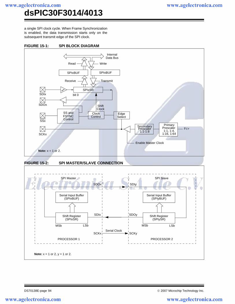
dsPIC30F3014/4013
DS70138E-page 94 © 2007 Microchip Technology Inc.
a single SPI clock cycle. When Frame Synchronizationis enabled, the data transmission starts only on thesubsequent transmit edge of the SPI clock.
FIGURE 15-1: SPI BLOCK DIAGRAM
FIGURE 15-2: SPI MASTER/SLAVE CONNECTION
Note: x = 1 or 2.
Read Write
InternalData Bus
SDIx
SDOx
SSx
SCKx
SPIxSR
SPIxBUF
bit 0
ShiftClock
EdgeSelect
Enable Master Clock
SS and
Control
ClockControl
Transmit
SPIxBUF
Receive
FSYNC
FCY
Primary
1:1, 1:4,PrescalerSecondary
Prescaler1:1-1:8
1:16, 1:64
Serial Input Buffer(SPIxBUF)
Shift Register(SPIxSR)
MSb LSb
SDOx
SDIx
PROCESSOR 1
SCKx
SPI Master
Serial Input Buffer(SPIyBUF)
Shift Register(SPIySR)
LSbMSb
SDIy
SDOy
PROCESSOR 2
SCKy
SPI Slave
Serial Clock
Note: x = 1 or 2, y = 1 or 2.
© 2007 Microchip Technology Inc. DS70138E-page 95
dsPIC30F3014/4013
15.3 Slave Select Synchronization
The SSx pin allows a Synchronous Slave mode. TheSPI must be configured in SPI Slave mode with SSx pincontrol enabled (SSEN = 1). When the SSx pin is low,transmission and reception are enabled and the SDOxpin is driven. When SSx pin goes high, the SDOx pin isno longer driven. Also, the SPI module is resynchro-nized, and all counters/control circuitry are reset.Therefore, when the SSx pin is asserted low again,transmission/reception begins at the MSb even if SSxhad been de-asserted in the middle of a transmit/receive.
15.4 SPI Operation During CPU Sleep Mode
During Sleep mode, the SPI module is shut down. If theCPU enters Sleep mode while an SPI transaction is inprogress, then the transmission and reception isaborted.
The transmitter and receiver stop in Sleep mode.However, register contents are not affected by enteringor exiting Sleep mode.
15.5 SPI Operation During CPU Idle Mode
When the device enters Idle mode, all clock sourcesremain functional. The SPISIDL bit (SPIxSTAT<13>)determines if the SPI module stops or continues onIdle. If SPISIDL = 0, the module continues to operatewhen the CPU enters Idle mode. If SPISIDL = 1, themodule stops when the CPU enters Idle mode.
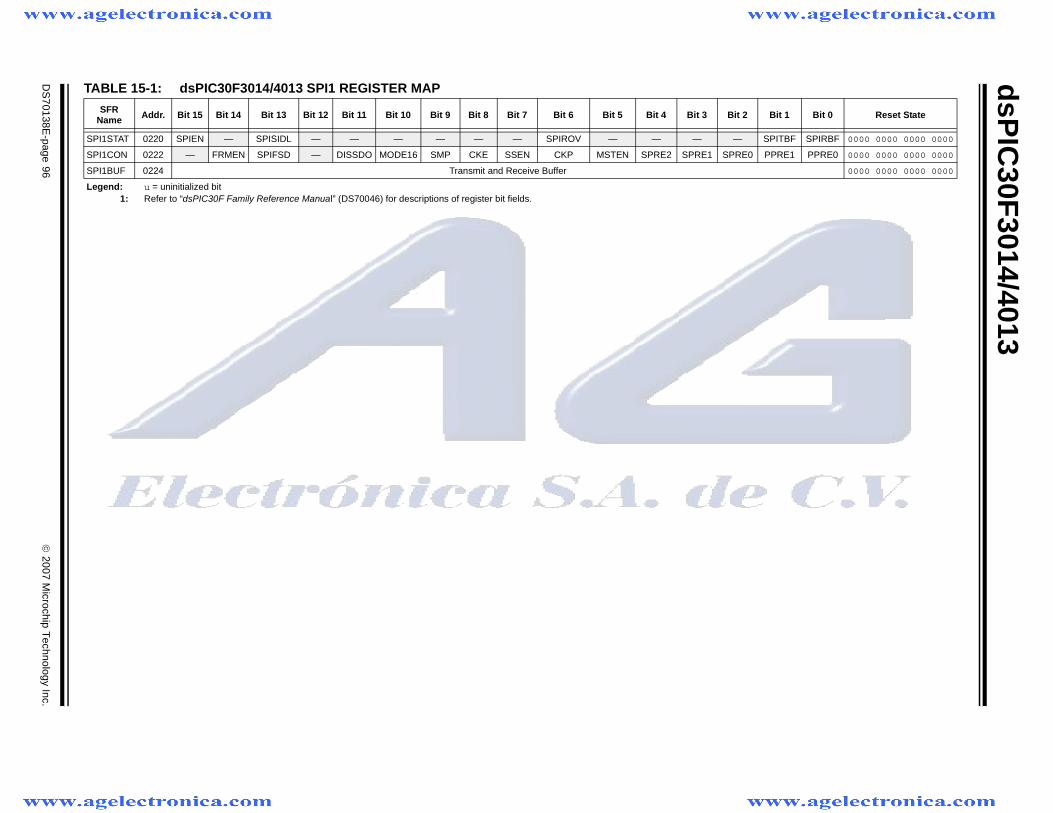
dsP
IC30F
3014/4013
DS
70138E-page 96
© 2007 M
icrochip Technology Inc.
TABLE 15-1: dsPIC30F3014/4013 SPI1 REGISTER MAP
SFR Name Addr. Bit 15 Bit 14 Bit 13 Bit 12 Bit 11 Bit 10 Bit 9 Bit 8 Bit 7 Bit 6 Bit 5 Bit 4 Bit 3 Bit 2 Bit 1 Bit 0 Reset State
SPI1STAT 0220 SPIEN — SPISIDL — — — — — — SPIROV — — — — SPITBF SPIRBF 0000 0000 0000 0000
SPI1CON 0222 — FRMEN SPIFSD — DISSDO MODE16 SMP CKE SSEN CKP MSTEN SPRE2 SPRE1 SPRE0 PPRE1 PPRE0 0000 0000 0000 0000
SPI1BUF 0224 Transmit and Receive Buffer 0000 0000 0000 0000
Legend: u = uninitialized bit1: Refer to “dsPIC30F Family Reference Manual” (DS70046) for descriptions of register bit fields.
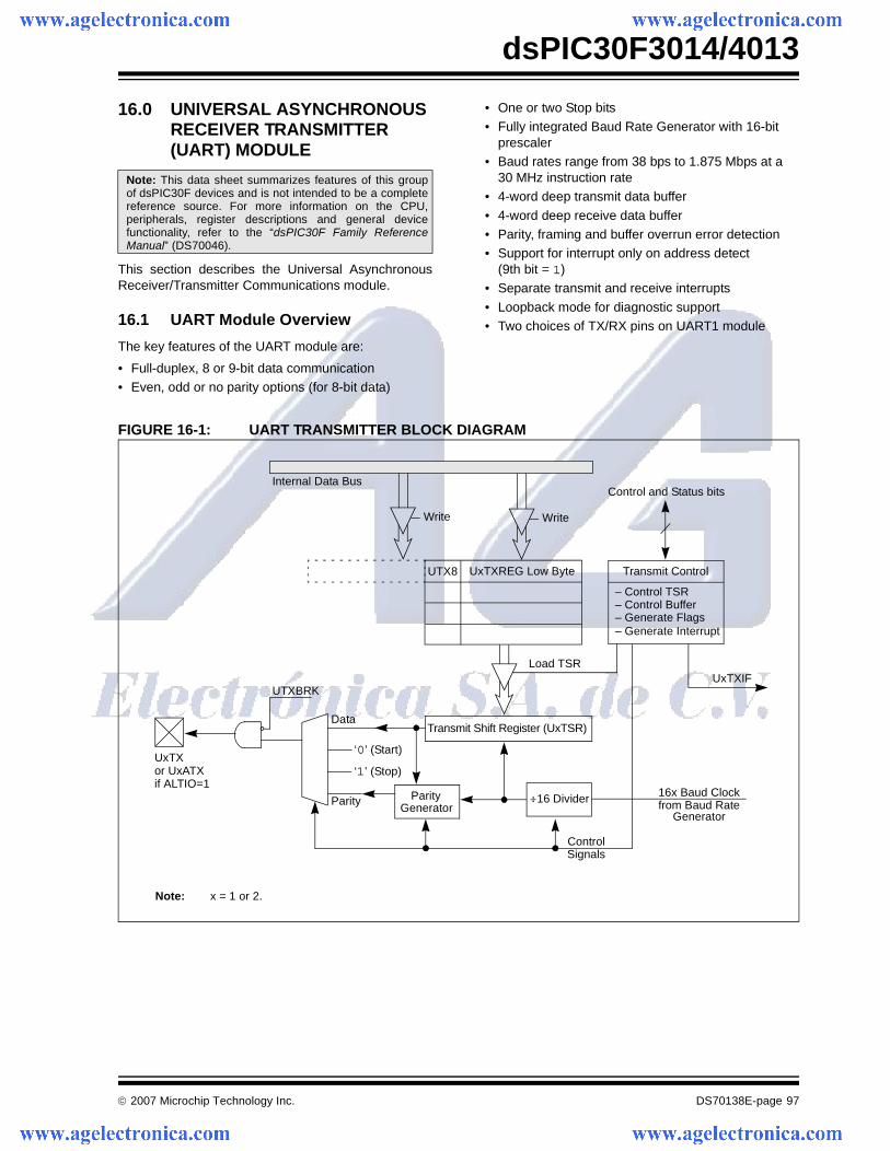
© 2007 Microchip Technology Inc. DS70138E-page 97
dsPIC30F3014/4013
16.0 UNIVERSAL ASYNCHRONOUS RECEIVER TRANSMITTER (UART) MODULE
This section describes the Universal AsynchronousReceiver/Transmitter Communications module.
16.1 UART Module Overview
The key features of the UART module are:
• Full-duplex, 8 or 9-bit data communication• Even, odd or no parity options (for 8-bit data)
• One or two Stop bits• Fully integrated Baud Rate Generator with 16-bit
prescaler• Baud rates range from 38 bps to 1.875 Mbps at a
30 MHz instruction rate• 4-word deep transmit data buffer
• 4-word deep receive data buffer• Parity, framing and buffer overrun error detection• Support for interrupt only on address detect
(9th bit = 1)• Separate transmit and receive interrupts
• Loopback mode for diagnostic support• Two choices of TX/RX pins on UART1 module
FIGURE 16-1: UART TRANSMITTER BLOCK DIAGRAM
Note: This data sheet summarizes features of this groupof dsPIC30F devices and is not intended to be a completereference source. For more information on the CPU,peripherals, register descriptions and general devicefunctionality, refer to the “dsPIC30F Family ReferenceManual” (DS70046).
Write Write
UTX8 UxTXREG Low Byte
Load TSR
Transmit Control
– Control TSR– Control Buffer– Generate Flags– Generate Interrupt
Control and Status bits
UxTXIF
Data
‘0’ (Start)
‘1’ (Stop)
Parity ParityGenerator
Transmit Shift Register (UxTSR)
16 Divider
ControlSignals
16x Baud Clockfrom Baud Rate
Generator
Internal Data Bus
UTXBRK
UxTX
Note: x = 1 or 2.
or UxATXif ALTIO=1
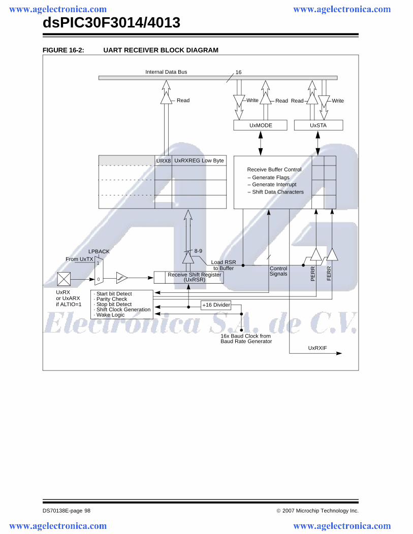
dsPIC30F3014/4013
DS70138E-page 98 © 2007 Microchip Technology Inc.
FIGURE 16-2: UART RECEIVER BLOCK DIAGRAM
Read
URX8 UxRXREG Low Byte
Load RSR
UxMODE
Receive Buffer Control
– Generate Flags– Generate Interrupt
UxRXIF
UxRX · Start bit Detect
Receive Shift Register
16 Divider
ControlSignals
UxSTA
– Shift Data Characters
Read ReadWrite Write
to Buffer
8-9
(UxRSR) PE
RR
FE
RR
· Parity Check· Stop bit Detect· Shift Clock Generation· Wake Logic
16Internal Data Bus
1
0
LPBACKFrom UxTX
16x Baud Clock fromBaud Rate Generator
or UxARXif ALTIO=1
© 2007 Microchip Technology Inc. DS70138E-page 99
dsPIC30F3014/4013
16.2 Enabling and Setting Up UART
16.2.1 ENABLING THE UART
The UART module is enabled by setting the UARTENbit in the UxMODE register (where x = 1 or 2). Onceenabled, the UxTX and UxRX pins are configured as anoutput and an input, respectively, overriding the TRISand LAT register bit settings for the corresponding I/Oport pins. The UxTX pin is at logic ‘1’ when notransmission is taking place.
16.2.2 DISABLING THE UART
The UART module is disabled by clearing the UARTENbit in the UxMODE register. This is the default stateafter any Reset. If the UART is disabled, all I/O pinsoperate as port pins under the control of the LAT andTRIS bits of the corresponding port pins.
Disabling the UART module resets the buffers to emptystates. Any data characters in the buffers are lost andthe baud rate counter is reset.
All error and status flags associated with the UARTmodule are reset when the module is disabled. TheURXDA, OERR, FERR, PERR, UTXEN, UTXBRK andUTXBF bits are cleared, whereas RIDLE and TRMTare set. Other control bits, including ADDEN,URXISEL<1:0>, UTXISEL, as well as the UxMODEand UxBRG registers, are not affected.
Clearing the UARTEN bit while the UART is activeaborts all pending transmissions and receptions andresets the module, as defined above. Re-enabling theUART restarts the UART in the same configuration.
16.2.3 ALTERNATE I/O
The alternate I/O function is enabled by setting theALTIO bit (UxMODE<10>). If ALTIO = 1, the UxATXand UxARX pins (alternate transmit and alternatereceive pins, respectively) are used by the UART mod-ule instead of the UxTX and UxRX pins. If ALTIO = 0,the UxTX and UxRX pins are used by the UARTmodule.
16.2.4 SETTING UP DATA, PARITY AND STOP BIT SELECTIONS
Control bits PDSEL<1:0> in the UxMODE register areused to select the data length and parity used in thetransmission. The data length may either be 8 bits witheven, odd or no parity, or 9 bits with no parity.
The STSEL bit determines whether one or two Stop bitsare used during data transmission.
The default (power-on) setting of the UART is 8 bits, noparity and 1 Stop bit (typically represented as 8, N, 1).
16.3 Transmitting Data
16.3.1 TRANSMITTING IN 8-BIT DATA MODE
The following steps must be performed in order totransmit 8-bit data:
1. Set up the UART:First, the data length, parity and number of Stopbits must be selected. Then, the transmit andreceive interrupt enable and priority bits aresetup in the UxMODE and UxSTA registers.Also, the appropriate baud rate value must bewritten to the UxBRG register.
2. Enable the UART by setting the UARTEN bit(UxMODE<15>).
3. Set the UTXEN bit (UxSTA<10>), therebyenabling a transmission.
4. Write the byte to be transmitted to the lower byteof UxTXREG. The value is transferred to theTransmit Shift register (UxTSR) immediately,and the serial bit stream starts shifting out duringthe next rising edge of the baud clock. Alterna-tively, the data byte can be written while UTXEN= 0, following which, the user can set UTXEN.This causes the serial bit stream to begin imme-diately because the baud clock starts from acleared state.
5. A transmit interrupt is generated, depending onthe value of the interrupt control bit UTXISEL(UxSTA<15>).
16.3.2 TRANSMITTING IN 9-BIT DATA MODE
The sequence of steps involved in the transmission of9-bit data is similar to 8-bit transmission, except that a16-bit data word (of which the upper 7 bits are alwaysclear) must be written to the UxTXREG register.
16.3.3 TRANSMIT BUFFER (UXTXB)
The transmit buffer is 9 bits wide and 4 charactersdeep. Including the Transmit Shift register (UxTSR),the user effectively has a 5-deep FIFO (First-In, First-Out) buffer. The UTXBF Status bit (UxSTA<9>)indicates whether the transmit buffer is full.
If a user attempts to write to a full buffer, the new datais not accepted into the FIFO, and no data shift occurswithin the buffer. This enables recovery from a bufferoverrun condition.
The FIFO is reset during any device Reset but is notaffected when the device enters or wakes up from aPower-Saving mode.
dsPIC30F3014/4013
DS70138E-page 100 © 2007 Microchip Technology Inc.
16.3.4 TRANSMIT INTERRUPT
The transmit interrupt flag (U1TXIF or U2TXIF) islocated in the corresponding interrupt flag register.
The transmitter generates an edge to set the UxTXIFbit. The condition for generating the interrupt dependson the UTXISEL control bit:
a) If UTXISEL = 0, an interrupt is generated whena word is transferred from the transmit buffer tothe Transmit Shift register (UxTSR). This meansthat the transmit buffer has at least one emptyword.
b) If UTXISEL = 1, an interrupt is generated whena word is transferred from the transmit buffer tothe Transmit Shift register (UxTSR) and thetransmit buffer is empty.
Switching between the two Interrupt modes duringoperation is possible and sometimes offers moreflexibility.
16.3.5 TRANSMIT BREAK
Setting the UTXBRK bit (UxSTA<11>) causes theUxTX line to be driven to logic ‘0’. The UTXBRK bitoverrides all transmission activity. Therefore, the usershould generally wait for the transmitter to be Idlebefore setting UTXBRK.
To send a Break character, the UTXBRK bit must be setby software and must remain set for a minimum of 13baud clock cycles. The UTXBRK bit is then cleared bysoftware to generate Stop bits. The user must wait fora duration of at least one or two baud clock cycles inorder to ensure a valid Stop bit(s) before reloading theUxTXB, or starting other transmitter activity. Transmis-sion of a Break character does not generate a transmitinterrupt.
16.4 Receiving Data
16.4.1 RECEIVING IN 8-BIT OR 9-BIT DATA MODE
The following steps must be performed while receiving8-bit or 9-bit data:
1. Set up the UART (see Section 16.3.1 “Trans-mitting in 8-Bit Data Mode”).
2. Enable the UART (see Section 16.3.1 “Trans-mitting in 8-Bit Data Mode”).
3. A receive interrupt is generated when one ormore data words have been received, depend-ing on the receive interrupt settings specified bythe URXISEL bits (UxSTA<7:6>).
4. Read the OERR bit to determine if an overrunerror has occurred. The OERR bit must be resetin software.
5. Read the received data from UxRXREG. The actof reading UxRXREG moves the next word tothe top of the receive FIFO, and the PERR and
FERR values are updated.
16.4.2 RECEIVE BUFFER (UXRXB)
The receive buffer is 4 words deep. Including theReceive Shift register (UxRSR), the user effectivelyhas a 5-word deep FIFO buffer.
URXDA (UxSTA<0>) = 1 indicates that the receivebuffer has data available. URXDA = 0 means that thebuffer is empty. If a user attempts to read an emptybuffer, the old values in the buffer are read and no datashift occurs within the FIFO.
The FIFO is reset during any device Reset. It is notaffected when the device enters or wakes up from aPower-Saving mode.
16.4.3 RECEIVE INTERRUPT
The receive interrupt flag (U1RXIF or U2RXIF) can beread from the corresponding interrupt flag register. Theinterrupt flag is set by an edge generated by thereceiver. The condition for setting the receive interruptflag depends on the settings specified by theURXISEL<1:0> (UxSTA<7:6>) control bits.
a) If URXISEL<1:0> = 00 or 01, an interrupt is gen-erated every time a data word is transferredfrom the Receive Shift register (UxRSR) to thereceive buffer. There may be one or morecharacters in the receive buffer.
b) If URXISEL<1:0> = 10, an interrupt is generatedwhen a word is transferred from the Receive Shiftregister (UxRSR) to the receive buffer, which as aresult of the transfer, contains 3 characters.
c) If URXISEL<1:0> = 11, an interrupt is set whena word is transferred from the Receive Shiftregister (UxRSR) to the receive buffer, which asa result of the transfer, contains 4 characters(i.e., becomes full).
Switching between the Interrupt modes during opera-tion is possible, though generally not advisable duringnormal operation.
16.5 Reception Error Handling
16.5.1 RECEIVE BUFFER OVERRUN ERROR (OERR BIT)
The OERR bit (UxSTA<1>) is set if all of the followingconditions occur:
a) The receive buffer is full.b) The Receive Shift register is full, but unable to
transfer the character to the receive buffer.c) The Stop bit of the character in the UxRSR is
detected, indicating that the UxRSR needs totransfer the character to the buffer.
© 2007 Microchip Technology Inc. DS70138E-page 101
dsPIC30F3014/4013
Once OERR is set, no further data is shifted in UxRSR(until the OERR bit is cleared in software or a Resetoccurs). The data held in UxRSR and UxRXREGremains valid.
16.5.2 FRAMING ERROR (FERR)
The FERR bit (UxSTA<2>) is set if a ‘0’ is detectedinstead of a Stop bit. If two Stop bits are selected, bothStop bits must be ‘1’, otherwise FERR is set. The read-only FERR bit is buffered along with the received data.It is cleared on any Reset.
16.5.3 PARITY ERROR (PERR)
The PERR bit (UxSTA<3>) is set if the parity of thereceived word is incorrect. This error bit is applicableonly if a Parity mode (odd or even) is selected. Theread-only PERR bit is buffered along with the receiveddata bytes. It is cleared on any Reset.
16.5.4 IDLE STATUS
When the receiver is active (i.e., between the initialdetection of the Start bit and the completion of the Stopbit), the RIDLE bit (UxSTA<4>) is ‘0’. Between the com-pletion of the Stop bit and detection of the next Start bit,the RIDLE bit is ‘1’, indicating that the UART is Idle.
16.5.5 RECEIVE BREAK
The receiver counts and expects a certain number of bittimes based on the values programmed in the PDSEL(UxMODE<2:1>) and STSEL (UxMODE<0>) bits.
If the break is longer than 13 bit times, the reception isconsidered complete after the number of bit timesspecified by PDSEL and STSEL. The URXDA bit is set,FERR is set, zeros are loaded into the receive FIFO,interrupts are generated if appropriate and the RIDLEbit is set.
When the module receives a long break signal and thereceiver has detected the Start bit, the data bits and theinvalid Stop bit (which sets the FERR), the receivermust wait for a valid Stop bit before looking for the nextStart bit. It cannot assume that the break condition onthe line is the next Start bit.
Break is regarded as a character containing all ‘0’s withthe FERR bit set. The Break character is loaded intothe buffer. No further reception can occur until a Stop bitis received. Note that RIDLE goes high when the Stopbit has not yet been received.
16.6 Address Detect Mode
Setting the ADDEN bit (UxSTA<5>) enables thisspecial mode in which a 9th bit (URX8) value of ‘1’identifies the received word as an address, rather thandata. This mode is only applicable for 9-bit datacommunication. The URXISEL control bit does nothave any impact on interrupt generation in this modesince an interrupt (if enabled) is generated every timethe received word has the 9th bit set.
16.7 Loopback Mode
Setting the LPBACK bit enables this special mode inwhich the UxTX pin is internally connected to the UxRXpin. When configured for the Loopback mode, theUxRX pin is disconnected from the internal UARTreceive logic. However, the UxTX pin still functions asin a normal operation.
To select this mode:
a) Configure UART for desired mode of operation.
b) Set LPBACK = 1 to enable Loopback mode.c) Enable transmission as defined in Section 16.3
“Transmitting Data”.
16.8 Baud Rate Generator
The UART has a 16-bit Baud Rate Generator to allowmaximum flexibility in baud rate generation. The BaudRate Generator register (UxBRG) is readable andwritable. The baud rate is computed as follows:
BRG = 16-bit value held in UxBRG register (0 through 65535)
FCY = Instruction Clock Rate (1/TCY)
The Baud Rate is given by Equation 16-1.
EQUATION 16-1: BAUD RATE
Therefore, the maximum baud rate possible is:
FCY /16 (if BRG = 0),
and the minimum baud rate possible is:
FCY / (16* 65536).
With a full 16-bit Baud Rate Generator at 30 MIPSoperation, the minimum baud rate achievable is28.5 bps.
Baud Rate = FCY / (16*(BRG+1))
dsPIC30F3014/4013
DS70138E-page 102 © 2007 Microchip Technology Inc.
16.9 Auto-Baud Support
To allow the system to determine baud rates ofreceived characters, the input can be optionally linkedto a capture input (IC1 for UART1, IC2 for UART2). Toenable this mode, the user must program the inputcapture module to detect the falling and rising edges ofthe Start bit.
16.10 UART Operation During CPU Sleep and Idle Modes
16.10.1 UART OPERATION DURING CPU SLEEP MODE
When the device enters Sleep mode, all clock sourcesto the module are shut down and stay at logic ‘0’. Ifentry into Sleep mode occurs while a transmission is inprogress, then the transmission is aborted. The UxTXpin is driven to logic ‘1’. Similarly, if entry into Sleepmode occurs while a reception is in progress, then thereception is aborted. The UxSTA, UxMODE, transmitand receive registers and buffers, and the UxBRGregister are not affected by Sleep mode.
If the WAKE bit (UxMODE<7>) is set before the deviceenters Sleep mode, a falling edge on the UxRX pingenerates a receive interrupt. The Receive InterruptSelect mode bit (URXISEL) has no effect for this func-tion. If the receive interrupt is enabled, this wakes thedevice up from Sleep. The UARTEN bit must be set inorder to generate a wake-up interrupt.
16.10.2 UART OPERATION DURING CPU IDLE MODE
For the UART, the USIDL bit determines if the modulestops or continues operation when the device entersIdle mode. If USIDL = 0, the module continuesoperation during Idle mode. If USIDL = 1, the modulestops on Idle.
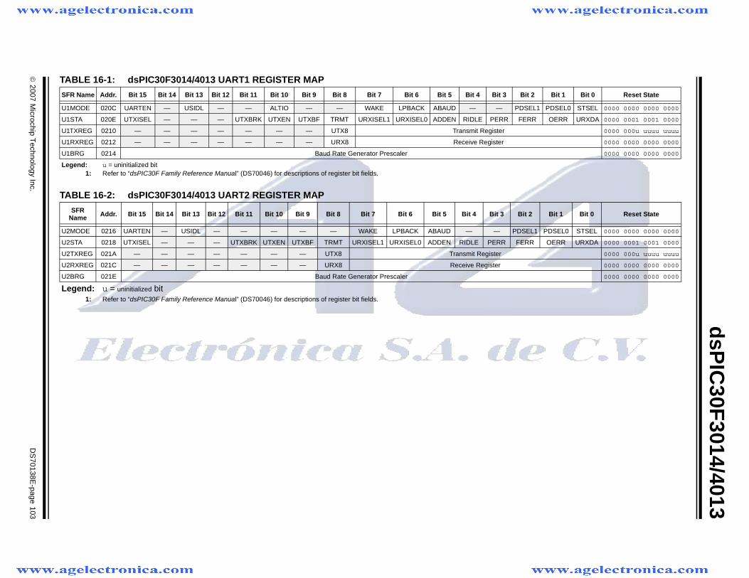
© 2007 M
icrochip Technology Inc.
DS
70138E-page 103
dsP
IC30F
3014/4013
TABLE 16-1: dsPIC30F3014/4013 UART1 REGISTER MAP
TABLE 16-2: dsPIC30F3014/4013 UART2 REGISTER MAP
SFR Name Addr. Bit 15 Bit 14 Bit 13 Bit 12 Bit 11 Bit 10 Bit 9 Bit 8 Bit 7 Bit 6 Bit 5 Bit 4 Bit 3 Bit 2 Bit 1 Bit 0 Reset State
U1MODE 020C UARTEN — USIDL — — ALTIO — — WAKE LPBACK ABAUD — — PDSEL1 PDSEL0 STSEL 0000 0000 0000 0000
U1STA 020E UTXISEL — — — UTXBRK UTXEN UTXBF TRMT URXISEL1 URXISEL0 ADDEN RIDLE PERR FERR OERR URXDA 0000 0001 0001 0000
U1TXREG 0210 — — — — — — — UTX8 Transmit Register 0000 000u uuuu uuuu
U1RXREG 0212 — — — — — — — URX8 Receive Register 0000 0000 0000 0000
U1BRG 0214 Baud Rate Generator Prescaler 0000 0000 0000 0000
Legend: u = uninitialized bit1: Refer to “dsPIC30F Family Reference Manual” (DS70046) for descriptions of register bit fields.
SFR Name Addr. Bit 15 Bit 14 Bit 13 Bit 12 Bit 11 Bit 10 Bit 9 Bit 8 Bit 7 Bit 6 Bit 5 Bit 4 Bit 3 Bit 2 Bit 1 Bit 0 Reset State
U2MODE 0216 UARTEN — USIDL — — — — — WAKE LPBACK ABAUD — — PDSEL1 PDSEL0 STSEL 0000 0000 0000 0000
U2STA 0218 UTXISEL — — — UTXBRK UTXEN UTXBF TRMT URXISEL1 URXISEL0 ADDEN RIDLE PERR FERR OERR URXDA 0000 0001 0001 0000
U2TXREG 021A — — — — — — — UTX8 Transmit Register 0000 000u uuuu uuuu
U2RXREG 021C — — — — — — — URX8 Receive Register 0000 0000 0000 0000
U2BRG 021E Baud Rate Generator Prescaler 0000 0000 0000 0000
Legend: u = uninitialized bit1: Refer to “dsPIC30F Family Reference Manual” (DS70046) for descriptions of register bit fields.

dsPIC30F3014/4013
DS70138E-page 104 © 2007 Microchip Technology Inc.
NOTES:
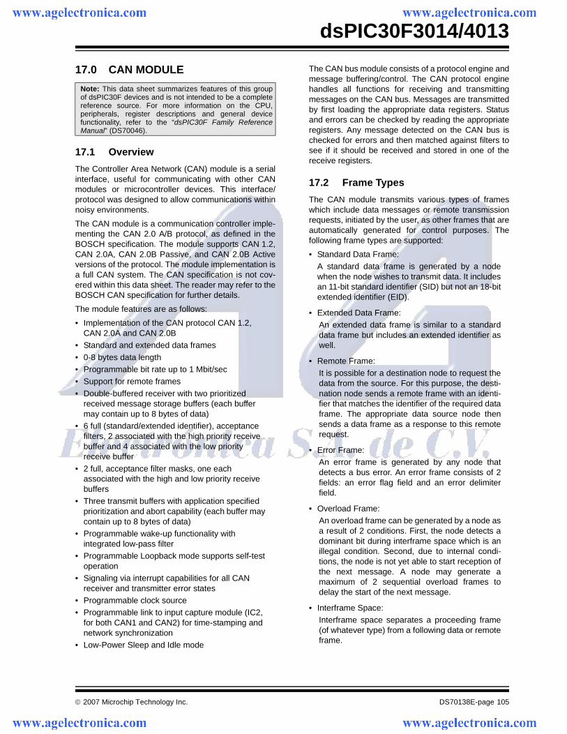
© 2007 Microchip Technology Inc. DS70138E-page 105
dsPIC30F3014/4013
17.0 CAN MODULE
17.1 Overview
The Controller Area Network (CAN) module is a serialinterface, useful for communicating with other CANmodules or microcontroller devices. This interface/protocol was designed to allow communications withinnoisy environments.
The CAN module is a communication controller imple-menting the CAN 2.0 A/B protocol, as defined in theBOSCH specification. The module supports CAN 1.2,CAN 2.0A, CAN 2.0B Passive, and CAN 2.0B Activeversions of the protocol. The module implementation isa full CAN system. The CAN specification is not cov-ered within this data sheet. The reader may refer to theBOSCH CAN specification for further details.
The module features are as follows:
• Implementation of the CAN protocol CAN 1.2, CAN 2.0A and CAN 2.0B
• Standard and extended data frames
• 0-8 bytes data length• Programmable bit rate up to 1 Mbit/sec• Support for remote frames
• Double-buffered receiver with two prioritized received message storage buffers (each buffer may contain up to 8 bytes of data)
• 6 full (standard/extended identifier), acceptance filters, 2 associated with the high priority receive buffer and 4 associated with the low priority receive buffer
• 2 full, acceptance filter masks, one each associated with the high and low priority receive buffers
• Three transmit buffers with application specified prioritization and abort capability (each buffer may contain up to 8 bytes of data)
• Programmable wake-up functionality with integrated low-pass filter
• Programmable Loopback mode supports self-test operation
• Signaling via interrupt capabilities for all CAN receiver and transmitter error states
• Programmable clock source• Programmable link to input capture module (IC2,
for both CAN1 and CAN2) for time-stamping and network synchronization
• Low-Power Sleep and Idle mode
The CAN bus module consists of a protocol engine andmessage buffering/control. The CAN protocol enginehandles all functions for receiving and transmittingmessages on the CAN bus. Messages are transmittedby first loading the appropriate data registers. Statusand errors can be checked by reading the appropriateregisters. Any message detected on the CAN bus ischecked for errors and then matched against filters tosee if it should be received and stored in one of thereceive registers.
17.2 Frame Types
The CAN module transmits various types of frameswhich include data messages or remote transmissionrequests, initiated by the user, as other frames that areautomatically generated for control purposes. Thefollowing frame types are supported:
• Standard Data Frame:A standard data frame is generated by a nodewhen the node wishes to transmit data. It includesan 11-bit standard identifier (SID) but not an 18-bitextended identifier (EID).
• Extended Data Frame:An extended data frame is similar to a standarddata frame but includes an extended identifier aswell.
• Remote Frame:It is possible for a destination node to request thedata from the source. For this purpose, the desti-nation node sends a remote frame with an identi-fier that matches the identifier of the required dataframe. The appropriate data source node thensends a data frame as a response to this remoterequest.
• Error Frame:An error frame is generated by any node thatdetects a bus error. An error frame consists of 2fields: an error flag field and an error delimiterfield.
• Overload Frame: An overload frame can be generated by a node asa result of 2 conditions. First, the node detects adominant bit during interframe space which is anillegal condition. Second, due to internal condi-tions, the node is not yet able to start reception ofthe next message. A node may generate amaximum of 2 sequential overload frames todelay the start of the next message.
• Interframe Space:Interframe space separates a proceeding frame(of whatever type) from a following data or remoteframe.
Note: This data sheet summarizes features of this groupof dsPIC30F devices and is not intended to be a completereference source. For more information on the CPU,peripherals, register descriptions and general devicefunctionality, refer to the “dsPIC30F Family ReferenceManual” (DS70046).
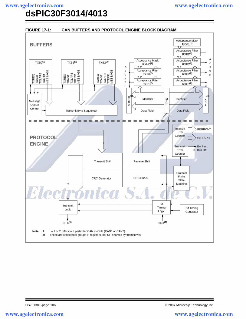
dsPIC30F3014/4013
DS70138E-page 106 © 2007 Microchip Technology Inc.
FIGURE 17-1: CAN BUFFERS AND PROTOCOL ENGINE BLOCK DIAGRAM
Acceptance FilterRXF2(2)
R(2)
XB1
Accept
Accept
Identifier
Data Field Data Field
Identifier
Acceptance MaskRXM1(2)
Acceptance FilterRXF3(2)
Acceptance FilterRXF4(2)
Acceptance FilterRXF5(2)
MAB
Acceptance MaskRXM0(2)
Acceptance FilterRXF0(2)
Acceptance FilterRXF1(2)
R(2)
XB0
TX
RE
Q
TXB2(2)
TX
AB
TT
XLA
RB
TX
ER
RM
ES
SA
GE
MessageQueueControl
Transmit Byte Sequencer
TX
RE
QTXB1(2)
TX
AB
TT
XLA
RB
TX
ER
RM
ES
SA
GE
TX
RE
Q
TXB0(2)
TX
AB
TT
XLA
RB
TX
ER
RM
ES
SA
GE
Receive ShiftTransmit Shift
ReceiveError
TransmitError
Protocol
RERRCNT
TERRCNT
Err PasBus Off
FiniteState
Machine
Counter
Counter
TransmitLogic
BitTimingLogic
CiTX(1) CiRX(1)
Bit TimingGenerator
PROTOCOLENGINE
BUFFERS
CRC CheckCRC Generator
Note 1: i = 1 or 2 refers to a particular CAN module (CAN1 or CAN2).2: These are conceptual groups of registers, not SFR names by themselves.
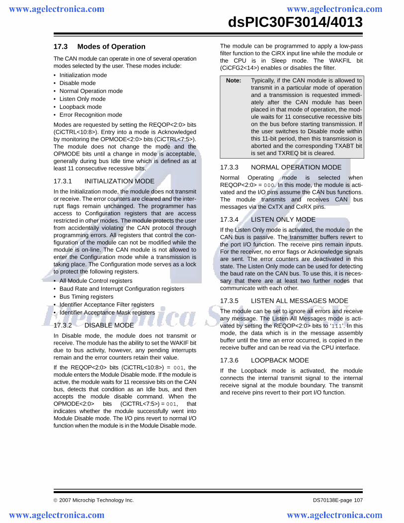
© 2007 Microchip Technology Inc. DS70138E-page 107
dsPIC30F3014/4013
17.3 Modes of Operation
The CAN module can operate in one of several operationmodes selected by the user. These modes include:
• Initialization mode• Disable mode• Normal Operation mode• Listen Only mode• Loopback mode• Error Recognition mode
Modes are requested by setting the REQOP<2:0> bits(CiCTRL<10:8>). Entry into a mode is Acknowledgedby monitoring the OPMODE<2:0> bits (CiCTRL<7:5>).The module does not change the mode and theOPMODE bits until a change in mode is acceptable,generally during bus Idle time which is defined as atleast 11 consecutive recessive bits.
17.3.1 INITIALIZATION MODE
In the Initialization mode, the module does not transmitor receive. The error counters are cleared and the inter-rupt flags remain unchanged. The programmer hasaccess to Configuration registers that are accessrestricted in other modes. The module protects the userfrom accidentally violating the CAN protocol throughprogramming errors. All registers that control the con-figuration of the module can not be modified while themodule is on-line. The CAN module is not allowed toenter the Configuration mode while a transmission istaking place. The Configuration mode serves as a lockto protect the following registers.
• All Module Control registers• Baud Rate and Interrupt Configuration registers • Bus Timing registers • Identifier Acceptance Filter registers • Identifier Acceptance Mask registers
17.3.2 DISABLE MODE
In Disable mode, the module does not transmit orreceive. The module has the ability to set the WAKIF bitdue to bus activity, however, any pending interruptsremain and the error counters retain their value.
If the REQOP<2:0> bits (CiCTRL<10:8>) = 001, themodule enters the Module Disable mode. If the module isactive, the module waits for 11 recessive bits on the CANbus, detects that condition as an Idle bus, and thenaccepts the module disable command. When theOPMODE<2:0> bits (CiCTRL<7:5>) = 001, thatindicates whether the module successfully went intoModule Disable mode. The I/O pins revert to normal I/Ofunction when the module is in the Module Disable mode.
The module can be programmed to apply a low-passfilter function to the CiRX input line while the module orthe CPU is in Sleep mode. The WAKFIL bit(CiCFG2<14>) enables or disables the filter.
17.3.3 NORMAL OPERATION MODE
Normal Operating mode is selected whenREQOP<2:0> = 000. In this mode, the module is acti-vated and the I/O pins assume the CAN bus functions.The module transmits and receives CAN busmessages via the CxTX and CxRX pins.
17.3.4 LISTEN ONLY MODE
If the Listen Only mode is activated, the module on theCAN bus is passive. The transmitter buffers revert tothe port I/O function. The receive pins remain inputs.For the receiver, no error flags or Acknowledge signalsare sent. The error counters are deactivated in thisstate. The Listen Only mode can be used for detectingthe baud rate on the CAN bus. To use this, it is neces-sary that there are at least two further nodes thatcommunicate with each other.
17.3.5 LISTEN ALL MESSAGES MODE
The module can be set to ignore all errors and receiveany message. The Listen All Messages mode is acti-vated by setting the REQOP<2:0> bits to ‘111’. In thismode, the data which is in the message assemblybuffer until the time an error occurred, is copied in thereceive buffer and can be read via the CPU interface.
17.3.6 LOOPBACK MODE
If the Loopback mode is activated, the moduleconnects the internal transmit signal to the internalreceive signal at the module boundary. The transmitand receive pins revert to their port I/O function.
Note: Typically, if the CAN module is allowed totransmit in a particular mode of operationand a transmission is requested immedi-ately after the CAN module has beenplaced in that mode of operation, the mod-ule waits for 11 consecutive recessive bitson the bus before starting transmission. Ifthe user switches to Disable mode withinthis 11-bit period, then this transmission isaborted and the corresponding TXABT bitis set and TXREQ bit is cleared.
dsPIC30F3014/4013
DS70138E-page 108 © 2007 Microchip Technology Inc.
17.4 Message Reception
17.4.1 RECEIVE BUFFERS
The CAN bus module has 3 receive buffers. However,one of the receive buffers is always committed to mon-itoring the bus for incoming messages. This buffer iscalled the Message Assembly Buffer (MAB). So thereare 2 receive buffers visible, denoted as RXB0 andRXB1, that can essentially instantaneously receive acomplete message from the protocol engine.
All messages are assembled by the MAB and are trans-ferred to the RXBn buffers only if the acceptance filtercriterion are met. When a message is received, theRXnIF flag (CiINRF<0> or CiINRF<1>) is set. This bitcan only be set by the module when a message isreceived. The bit is cleared by the CPU when it has com-pleted processing the message in the buffer. If theRXnIE bit (CiINTE<0> or CiINTE<1>) is set, an interruptis generated when a message is received.
RXF0 and RXF1 filters with RXM0 mask are associatedwith RXB0. The filters RXF2, RXF3, RXF4 and RXF5,and the mask RXM1 are associated with RXB1.
17.4.2 MESSAGE ACCEPTANCE FILTERS
The message acceptance filters and masks are used todetermine if a message in the message assemblybuffer should be loaded into either of the receive buff-ers. Once a valid message has been received into theMessage Assembly Buffer (MAB), the identifier fields ofthe message are compared to the filter values. If thereis a match, that message is loaded into the appropriatereceive buffer.
The acceptance filter looks at incoming messages forthe RXIDE bit (CiRXnSID<0>) to determine how tocompare the identifiers. If the RXIDE bit is clear, themessage is a standard frame and only filters with theEXIDE bit (CiRXFnSID<0>) clear are compared. If theRXIDE bit is set, the message is an extended frameand only filters with the EXIDE bit set are compared.
17.4.3 MESSAGE ACCEPTANCE FILTER MASKS
The mask bits essentially determine which bits to applythe filter to. If any mask bit is set to a zero, that bit isautomatically accepted regardless of the filter bit.There are two programmable acceptance filter masksassociated with the receive buffers, one for each buffer.
17.4.4 RECEIVE OVERRUN
An overrun condition occurs when the MessageAssembly Buffer (MAB) has assembled a validreceived message, the message is accepted throughthe acceptance filters, and when the receive bufferassociated with the filter has not been designated asclear of the previous message.
The overrun error flag, RXnOVR (CiINTF<15> orCiINTF<14>), and the ERRIF bit (CiINTF<5>) are setand the message in the MAB is discarded.
If the DBEN bit is clear, RXB1 and RXB0 operate inde-pendently. When this is the case, a message intendedfor RXB0 is not diverted into RXB1 if RXB0 contains anunread message, and the RX0OVR bit is set.
If the DBEN bit is set, the overrun for RXB0 is handleddifferently. If a valid message is received for RXB0 andRXFUL = 1 it indicates that RXB0 is full andRXFUL = 0 indicates that RXB1 is empty, the messagefor RXB0 is loaded into RXB1. An overrun error is notgenerated for RXB0. If a valid message is received forRXB0 and RXFUL = 1, indicates that both RXB0 andRXB1 are full, the message is lost and an overrun isindicated for RXB1.
17.4.5 RECEIVE ERRORS
The CAN module detects the following receive errors:
• Cyclic Redundancy Check (CRC) error
• Bit Stuffing error• Invalid Message Receive Error
These receive errors do not generate an interrupt.However, the receive error counter is incremented byone in case one of these errors occur. The RXWAR bit(CiINTF<9>) indicates that the receive error counterhas reached the CPU warning limit of 96 and aninterrupt is generated.
17.4.6 RECEIVE INTERRUPTS
Receive interrupts can be divided into 3 major groups,each including various conditions that generateinterrupts:
• Receive Interrupt:A message has been successfully received andloaded into one of the receive buffers. This inter-rupt is activated immediately after receiving theEnd-of-Frame (EOF) field. Reading the RXnIF flagindicates which receive buffer caused theinterrupt.
• Wake-up Interrupt:The CAN module has woken up from Disablemode or the device has woken up from Sleepmode.
© 2007 Microchip Technology Inc. DS70138E-page 109
dsPIC30F3014/4013
• Receive Error Interrupts:A receive error interrupt is indicated by the ERRIFbit. This bit shows that an error conditionoccurred. The source of the error can be deter-mined by checking the bits in the CAN InterruptSTATUS register, CiINTF.
- Invalid Message Received:If any type of error occurred during reception ofthe last message, an error is indicated by theIVRIF bit.
- Receiver Overrun:The RXnOVR bit indicates that an overruncondition occurred.
- Receiver Warning: The RXWAR bit indicates that the Receive ErrorCounter (RERRCNT<7:0>) has reached thewarning limit of 96.
- Receiver Error Passive:The RXEP bit indicates that the Receive ErrorCounter has exceeded the error passive limit of127 and the module has gone into error passivestate.
17.5 Message Transmission
17.5.1 TRANSMIT BUFFERS
The CAN module has three transmit buffers. Each ofthe three buffers occupies 14 bytes of data. Eight of thebytes are the maximum 8 bytes of the transmitted mes-sage. Five bytes hold the standard and extendedidentifiers and other message arbitration information.
17.5.2 TRANSMIT MESSAGE PRIORITY
Transmit priority is a prioritization within each node ofthe pending transmittable messages. There are4 levels of transmit priority. If TXPRI<1:0>(CiTXnCON<1:0>, where n = 0, 1 or 2, represents aparticular transmit buffer) for a particular messagebuffer is set to ‘11’, that buffer has the highest priority.If TXPRI<1:0> for a particular message buffer is set to‘10’ or ‘01’, that buffer has an intermediate priority. IfTXPRI<1:0> for a particular message buffer is ‘00’, thatbuffer has the lowest priority.
17.5.3 TRANSMISSION SEQUENCE
To initiate transmission of the message, the TXREQ bit(CiTXnCON<3>) must be set. The CAN bus moduleresolves any timing conflicts between setting of theTXREQ bit and the Start-of-Frame (SOF), ensuring that ifthe priority was changed, it is resolved correctly before theSOF occurs. When TXREQ is set, the TXABT(CiTXnCON<6>), TXLARB (CiTXnCON<5>) and TXERR(CiTXnCON<4>) flag bits are automatically cleared.
Setting TXREQ bit simply flags a message buffer asenqueued for transmission. When the module detectsan available bus, it begins transmitting the messagewhich has been determined to have the highest priority.
If the transmission completes successfully on the firstattempt, the TXREQ bit is cleared automatically and aninterrupt is generated if TX1IE was set.
If the message transmission fails, one of the errorcondition flags is set, and the TXREQ bit remains set,indicating that the message is still pending for transmis-sion. If the message encountered an error conditionduring the transmission attempt, the TXERR bit is set,and the error condition may cause an interrupt. If themessage loses arbitration during the transmissionattempt, the TXLARB bit is set. No interrupt isgenerated to signal the loss of arbitration.
17.5.4 ABORTING MESSAGE TRANSMISSION
The system can also abort a message by clearing theTXREQ bit associated with each message buffer. Set-ting the ABAT bit (CiCTRL<12>) requests an abort ofall pending messages. If the message has not yetstarted transmission, or if the message started but isinterrupted by loss of arbitration or an error, the abort isprocessed. The abort is indicated when the modulesets the TXABT bit and the TXnIF flag is not automati-cally set.
17.5.5 TRANSMISSION ERRORS
The CAN module detects the following transmissionerrors:
• Acknowledge error
• Form error• Bit error
These transmission errors do not necessarily generatean interrupt but are indicated by the transmission errorcounter. However, each of these errors causes thetransmission error counter to be incremented by one.Once the value of the error counter exceeds the valueof 96, the ERRIF (CiINTF<5>) and the TXWAR bit(CiINTF<10>) are set. Once the value of the errorcounter exceeds the value of 96, an interrupt isgenerated and the TXWAR bit in the Error Flag registeris set.
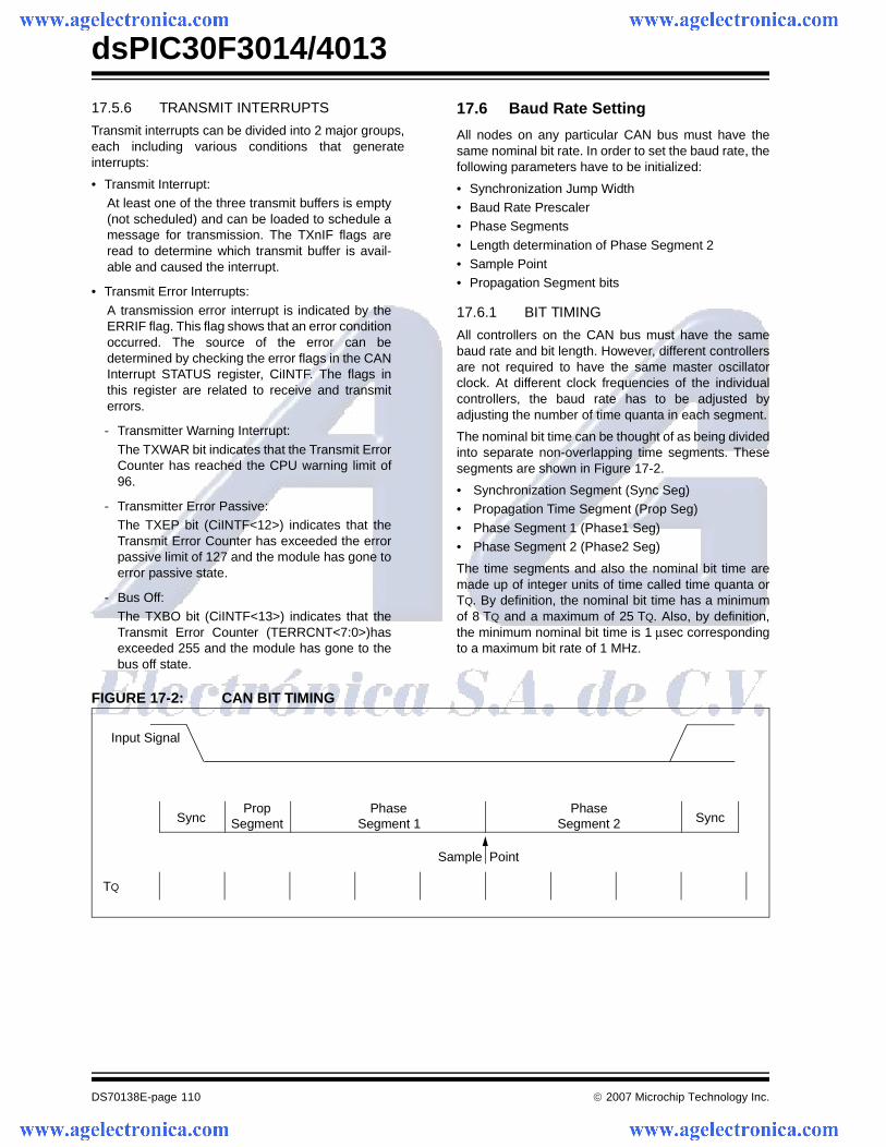
dsPIC30F3014/4013
DS70138E-page 110 © 2007 Microchip Technology Inc.
17.5.6 TRANSMIT INTERRUPTS
Transmit interrupts can be divided into 2 major groups,each including various conditions that generateinterrupts:
• Transmit Interrupt:At least one of the three transmit buffers is empty(not scheduled) and can be loaded to schedule amessage for transmission. The TXnIF flags areread to determine which transmit buffer is avail-able and caused the interrupt.
• Transmit Error Interrupts:
A transmission error interrupt is indicated by theERRIF flag. This flag shows that an error conditionoccurred. The source of the error can bedetermined by checking the error flags in the CANInterrupt STATUS register, CiINTF. The flags inthis register are related to receive and transmiterrors.
- Transmitter Warning Interrupt:
The TXWAR bit indicates that the Transmit ErrorCounter has reached the CPU warning limit of96.
- Transmitter Error Passive:The TXEP bit (CiINTF<12>) indicates that theTransmit Error Counter has exceeded the errorpassive limit of 127 and the module has gone toerror passive state.
- Bus Off: The TXBO bit (CiINTF<13>) indicates that theTransmit Error Counter (TERRCNT<7:0>)hasexceeded 255 and the module has gone to thebus off state.
17.6 Baud Rate Setting
All nodes on any particular CAN bus must have thesame nominal bit rate. In order to set the baud rate, thefollowing parameters have to be initialized:
• Synchronization Jump Width• Baud Rate Prescaler • Phase Segments
• Length determination of Phase Segment 2 • Sample Point • Propagation Segment bits
17.6.1 BIT TIMING
All controllers on the CAN bus must have the samebaud rate and bit length. However, different controllersare not required to have the same master oscillatorclock. At different clock frequencies of the individualcontrollers, the baud rate has to be adjusted byadjusting the number of time quanta in each segment.
The nominal bit time can be thought of as being dividedinto separate non-overlapping time segments. Thesesegments are shown in Figure 17-2.
• Synchronization Segment (Sync Seg)• Propagation Time Segment (Prop Seg)
• Phase Segment 1 (Phase1 Seg)• Phase Segment 2 (Phase2 Seg)
The time segments and also the nominal bit time aremade up of integer units of time called time quanta orTQ. By definition, the nominal bit time has a minimumof 8 TQ and a maximum of 25 TQ. Also, by definition,the minimum nominal bit time is 1 μsec correspondingto a maximum bit rate of 1 MHz.
FIGURE 17-2: CAN BIT TIMING
Input Signal
SyncProp
SegmentPhase
Segment 1Phase
Segment 2 Sync
Sample Point
TQ
© 2007 Microchip Technology Inc. DS70138E-page 111
dsPIC30F3014/4013
17.6.2 PRESCALER SETTING
There is a programmable prescaler with integral valuesranging from 1 to 64 in addition to a fixed divide-by-2 forclock generation. The Time Quantum (TQ) is a fixedunit of time derived from the oscillator period, shown inEquation 17-1, where FCAN is FCY (if the CANCKS bitis set) or 4FCY (if CANCKS is clear).
EQUATION 17-1: TIME QUANTUM FOR CLOCK GENERATION
17.6.3 PROPAGATION SEGMENT
This part of the bit time is used to compensate physicaldelay times within the network. These delay times con-sist of the signal propagation time on the bus line andthe internal delay time of the nodes. The propagationsegment can be programmed from 1 TQ to 8 TQ bysetting the PRSEG<2:0> bits (CiCFG2<2:0>).
17.6.4 PHASE SEGMENTS
The phase segments are used to optimally locate thesampling of the received bit within the transmitted bittime. The sampling point is between Phase1 Seg andPhase2 Seg. These segments are lengthened or short-ened by resynchronization. The end of the Phase1 Segdetermines the sampling point within a bit period. Thesegment is programmable from 1 TQ to 8 TQ. Phase2Seg provides delay to the next transmitted data transi-tion. The segment is programmable from 1 TQ to 8 TQ,or it may be defined to be equal to the greater ofPhase1 Seg or the information processing time (2 TQ).The Phase1 Seg is initialized by setting bitsSEG1PH<2:0> (CiCFG2<5:3>), and Phase2 Seg isinitialized by setting SEG2PH<2:0> (CiCFG2<10:8>).
The following requirement must be fulfilled while settingthe lengths of the phase segments:
Prop Seg + Phase1 Seg > = Phase2 Seg
17.6.5 SAMPLE POINT
The sample point is the point of time at which the buslevel is read and interpreted as the value of that respec-tive bit. The location is at the end of Phase1 Seg. If thebit timing is slow and contains many TQ, it is possible tospecify multiple sampling of the bus line at the samplepoint. The level determined by the CAN bus then corre-sponds to the result from the majority decision of threevalues. The majority samples are taken at the samplepoint and twice before with a distance of TQ/2. TheCAN module allows the user to choose betweensampling three times at the same point, or once at thesame point by setting or clearing the SAM bit(CiCFG2<6>).
Typically, the sampling of the bit should take place atabout 60-70% through the bit time depending on thesystem parameters.
17.6.6 SYNCHRONIZATION
To compensate for phase shifts between the oscillatorfrequencies of the different bus stations, each CANcontroller must be able to synchronize to the relevantsignal edge of the incoming signal. When an edge inthe transmitted data is detected, the logic compares thelocation of the edge to the expected time (synchronoussegment). The circuit then adjusts the values ofPhase1 Seg and Phase2 Seg. There are twomechanisms used to synchronize.
17.6.6.1 Hard Synchronization
Hard synchronization is only done when there is arecessive to dominant edge during bus Idle, indicatingthe start of a message. After hard synchronization, thebit-time counters are restarted with the synchronoussegment. Hard synchronization forces the edge whichhas caused the hard synchronization to lie within thesynchronization segment of the restarted bit time. If ahard synchronization is done, there will not be aresynchronization within that bit time.
17.6.6.2 Resynchronization
As a result of resynchronization, Phase1 Seg may belengthened or Phase2 Seg may be shortened. Theamount of lengthening or shortening of the phasebuffer segment has an upper bound known as the syn-chronization jump width, and is specified by theSJW<1:0> bits (CiCFG1<7:6>). The value of thesynchronization jump width is added to Phase1 Seg orsubtracted from Phase2 Seg. The resynchronizationjump width is programmable between 1 TQ and 4 TQ.
The following requirement must be fulfilled while settingthe SJW<1:0> bits:
Phase2 Seg > Synchronization Jump Width
Note: FCAN must not exceed 30 MHz. IfCANCKS = 0, then FCY must not exceed7.5 MHz.
TQ = 2 (BRP<5:0> + 1)/FCAN
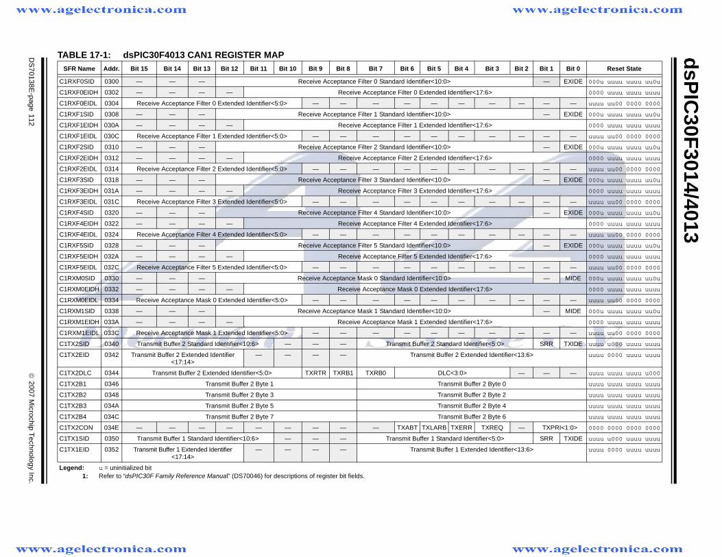
dsP
IC30F
3014/4013
DS
70138E-page 112
© 2007 M
icrochip Technology Inc.
TABLE 17-1: dsPIC30F4013 CAN1 REGISTER MAPSFR Name Addr. Bit 15 Bit 14 Bit 13 Bit 12 Bit 11 Bit 10 Bit 9 Bit 8 Bit 7 Bit 6 Bit 5 Bit 4 Bit 3 Bit 2 Bit 1 Bit 0 Reset State
C1RXF0SID 0300 — — — Receive Acceptance Filter 0 Standard Identifier<10:0> — EXIDE 000u uuuu uuuu uu0u
C1RXF0EIDH 0302 — — — — Receive Acceptance Filter 0 Extended Identifier<17:6> 0000 uuuu uuuu uuuu
C1RXF0EIDL 0304 Receive Acceptance Filter 0 Extended Identifier<5:0> — — — — — — — — — — uuuu uu00 0000 0000
C1RXF1SID 0308 — — — Receive Acceptance Filter 1 Standard Identifier<10:0> — EXIDE 000u uuuu uuuu uu0u
C1RXF1EIDH 030A — — — — Receive Acceptance Filter 1 Extended Identifier<17:6> 0000 uuuu uuuu uuuu
C1RXF1EIDL 030C Receive Acceptance Filter 1 Extended Identifier<5:0> — — — — — — — — — — uuuu uu00 0000 0000
C1RXF2SID 0310 — — — Receive Acceptance Filter 2 Standard Identifier<10:0> — EXIDE 000u uuuu uuuu uu0u
C1RXF2EIDH 0312 — — — — Receive Acceptance Filter 2 Extended Identifier<17:6> 0000 uuuu uuuu uuuu
C1RXF2EIDL 0314 Receive Acceptance Filter 2 Extended Identifier<5:0> — — — — — — — — — — uuuu uu00 0000 0000
C1RXF3SID 0318 — — — Receive Acceptance Filter 3 Standard Identifier<10:0> — EXIDE 000u uuuu uuuu uu0u
C1RXF3EIDH 031A — — — — Receive Acceptance Filter 3 Extended Identifier<17:6> 0000 uuuu uuuu uuuu
C1RXF3EIDL 031C Receive Acceptance Filter 3 Extended Identifier<5:0> — — — — — — — — — — uuuu uu00 0000 0000
C1RXF4SID 0320 — — — Receive Acceptance Filter 4 Standard Identifier<10:0> — EXIDE 000u uuuu uuuu uu0u
C1RXF4EIDH 0322 — — — — Receive Acceptance Filter 4 Extended Identifier<17:6> 0000 uuuu uuuu uuuu
C1RXF4EIDL 0324 Receive Acceptance Filter 4 Extended Identifier<5:0> — — — — — — — — — — uuuu uu00 0000 0000
C1RXF5SID 0328 — — — Receive Acceptance Filter 5 Standard Identifier<10:0> — EXIDE 000u uuuu uuuu uu0u
C1RXF5EIDH 032A — — — — Receive Acceptance Filter 5 Extended Identifier<17:6> 0000 uuuu uuuu uuuu
C1RXF5EIDL 032C Receive Acceptance Filter 5 Extended Identifier<5:0> — — — — — — — — — — uuuu uu00 0000 0000
C1RXM0SID 0330 — — — Receive Acceptance Mask 0 Standard Identifier<10:0> — MIDE 000u uuuu uuuu uu0u
C1RXM0EIDH 0332 — — — — Receive Acceptance Mask 0 Extended Identifier<17:6> 0000 uuuu uuuu uuuu
C1RXM0EIDL 0334 Receive Acceptance Mask 0 Extended Identifier<5:0> — — — — — — — — — — uuuu uu00 0000 0000
C1RXM1SID 0338 — — — Receive Acceptance Mask 1 Standard Identifier<10:0> — MIDE 000u uuuu uuuu uu0u
C1RXM1EIDH 033A — — — — Receive Acceptance Mask 1 Extended Identifier<17:6> 0000 uuuu uuuu uuuu
C1RXM1EIDL 033C Receive Acceptance Mask 1 Extended Identifier<5:0> — — — — — — — — — — uuuu uu00 0000 0000
C1TX2SID 0340 Transmit Buffer 2 Standard Identifier<10:6> — — — Transmit Buffer 2 Standard Identifier<5:0> SRR TXIDE uuuu u000 uuuu uuuu
C1TX2EID 0342 Transmit Buffer 2 Extended Identifier <17:14>
— — — — Transmit Buffer 2 Extended Identifier<13:6> uuuu 0000 uuuu uuuu
C1TX2DLC 0344 Transmit Buffer 2 Extended Identifier<5:0> TXRTR TXRB1 TXRB0 DLC<3:0> — — — uuuu uuuu uuuu u000
C1TX2B1 0346 Transmit Buffer 2 Byte 1 Transmit Buffer 2 Byte 0 uuuu uuuu uuuu uuuu
C1TX2B2 0348 Transmit Buffer 2 Byte 3 Transmit Buffer 2 Byte 2 uuuu uuuu uuuu uuuu
C1TX2B3 034A Transmit Buffer 2 Byte 5 Transmit Buffer 2 Byte 4 uuuu uuuu uuuu uuuu
C1TX2B4 034C Transmit Buffer 2 Byte 7 Transmit Buffer 2 Byte 6 uuuu uuuu uuuu uuuu
C1TX2CON 034E — — — — — — — — — TXABT TXLARB TXERR TXREQ — TXPRI<1:0> 0000 0000 0000 0000
C1TX1SID 0350 Transmit Buffer 1 Standard Identifier<10:6> — — — Transmit Buffer 1 Standard Identifier<5:0> SRR TXIDE uuuu u000 uuuu uuuu
C1TX1EID 0352 Transmit Buffer 1 Extended Identifier <17:14>
— — — — Transmit Buffer 1 Extended Identifier<13:6> uuuu 0000 uuuu uuuu
Legend: u = uninitialized bit1: Refer to “dsPIC30F Family Reference Manual” (DS70046) for descriptions of register bit fields.
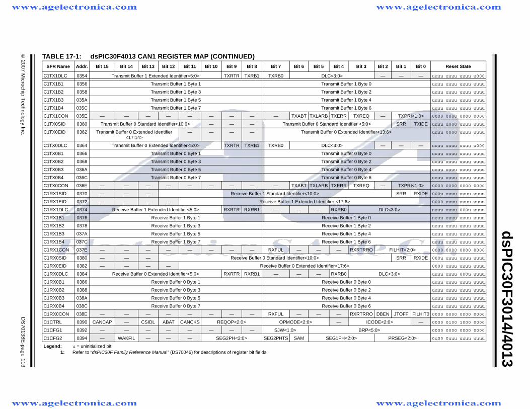
© 2007 M
icrochip Technology Inc.
DS
70138E-page 113
dsP
IC30F
3014/4013
C1TX1DLC 0354 Transmit Buffer 1 Extended Identifier<5:0> TXRTR TXRB1 TXRB0 DLC<3:0> — — — uuuu uuuu uuuu u000
C1TX1B1 0356 Transmit Buffer 1 Byte 1 Transmit Buffer 1 Byte 0 uuuu uuuu uuuu uuuu
C1TX1B2 0358 Transmit Buffer 1 Byte 3 Transmit Buffer 1 Byte 2 uuuu uuuu uuuu uuuu
C1TX1B3 035A Transmit Buffer 1 Byte 5 Transmit Buffer 1 Byte 4 uuuu uuuu uuuu uuuu
C1TX1B4 035C Transmit Buffer 1 Byte 7 Transmit Buffer 1 Byte 6 uuuu uuuu uuuu uuuu
C1TX1CON 035E — — — — — — — — — TXABT TXLARB TXERR TXREQ — TXPRI<1:0> 0000 0000 0000 0000
C1TX0SID 0360 Transmit Buffer 0 Standard Identifier<10:6> — — — Transmit Buffer 0 Standard Identifier <5:0> SRR TXIDE uuuu u000 uuuu uuuu
C1TX0EID 0362 Transmit Buffer 0 Extended Identifier <17:14>
— — — — Transmit Buffer 0 Extended Identifier<13:6> uuuu 0000 uuuu uuuu
C1TX0DLC 0364 Transmit Buffer 0 Extended Identifier<5:0> TXRTR TXRB1 TXRB0 DLC<3:0> — — — uuuu uuuu uuuu u000
C1TX0B1 0366 Transmit Buffer 0 Byte 1 Transmit Buffer 0 Byte 0 uuuu uuuu uuuu uuuu
C1TX0B2 0368 Transmit Buffer 0 Byte 3 Transmit Buffer 0 Byte 2 uuuu uuuu uuuu uuuu
C1TX0B3 036A Transmit Buffer 0 Byte 5 Transmit Buffer 0 Byte 4 uuuu uuuu uuuu uuuu
C1TX0B4 036C Transmit Buffer 0 Byte 7 Transmit Buffer 0 Byte 6 uuuu uuuu uuuu uuuu
C1TX0CON 036E — — — — — — — — — TXABT TXLARB TXERR TXREQ — TXPRI<1:0> 0000 0000 0000 0000
C1RX1SID 0370 — — — Receive Buffer 1 Standard Identifier<10:0> SRR RXIDE 000u uuuu uuuu uuuu
C1RX1EID 0372 — — — — Receive Buffer 1 Extended Identifier <17:6> 0000 uuuu uuuu uuuu
C1RX1DLC 0374 Receive Buffer 1 Extended Identifier<5:0> RXRTR RXRB1 — — — RXRB0 DLC<3:0> uuuu uuuu 000u uuuu
C1RX1B1 0376 Receive Buffer 1 Byte 1 Receive Buffer 1 Byte 0 uuuu uuuu uuuu uuuu
C1RX1B2 0378 Receive Buffer 1 Byte 3 Receive Buffer 1 Byte 2 uuuu uuuu uuuu uuuu
C1RX1B3 037A Receive Buffer 1 Byte 5 Receive Buffer 1 Byte 4 uuuu uuuu uuuu uuuu
C1RX1B4 037C Receive Buffer 1 Byte 7 Receive Buffer 1 Byte 6 uuuu uuuu uuuu uuuu
C1RX1CON 037E — — — — — — — — RXFUL — — — RXRTRRO FILHIT<2:0> 0000 0000 0000 0000
C1RX0SID 0380 — — — Receive Buffer 0 Standard Identifier<10:0> SRR RXIDE 000u uuuu uuuu uuuu
C1RX0EID 0382 — — — — Receive Buffer 0 Extended Identifier<17:6> 0000 uuuu uuuu uuuu
C1RX0DLC 0384 Receive Buffer 0 Extended Identifier<5:0> RXRTR RXRB1 — — — RXRB0 DLC<3:0> uuuu uuuu 000u uuuu
C1RX0B1 0386 Receive Buffer 0 Byte 1 Receive Buffer 0 Byte 0 uuuu uuuu uuuu uuuu
C1RX0B2 0388 Receive Buffer 0 Byte 3 Receive Buffer 0 Byte 2 uuuu uuuu uuuu uuuu
C1RX0B3 038A Receive Buffer 0 Byte 5 Receive Buffer 0 Byte 4 uuuu uuuu uuuu uuuu
C1RX0B4 038C Receive Buffer 0 Byte 7 Receive Buffer 0 Byte 6 uuuu uuuu uuuu uuuu
C1RX0CON 038E — — — — — — — — RXFUL — — — RXRTRRO DBEN JTOFF FILHIT0 0000 0000 0000 0000
C1CTRL 0390 CANCAP — CSIDL ABAT CANCKS REQOP<2:0> OPMODE<2:0> — ICODE<2:0> — 0000 0100 1000 0000
C1CFG1 0392 — — — — — — — — SJW<1:0> BRP<5:0> 0000 0000 0000 0000
C1CFG2 0394 — WAKFIL — — — SEG2PH<2:0> SEG2PHTS SAM SEG1PH<2:0> PRSEG<2:0> 0u00 0uuu uuuu uuuu
TABLE 17-1: dsPIC30F4013 CAN1 REGISTER MAP (CONTINUED)SFR Name Addr. Bit 15 Bit 14 Bit 13 Bit 12 Bit 11 Bit 10 Bit 9 Bit 8 Bit 7 Bit 6 Bit 5 Bit 4 Bit 3 Bit 2 Bit 1 Bit 0 Reset State
Legend: u = uninitialized bit1: Refer to “dsPIC30F Family Reference Manual” (DS70046) for descriptions of register bit fields.
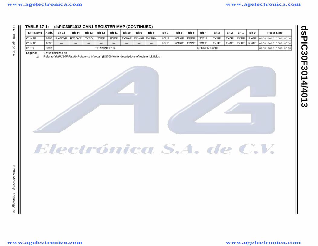
dsP
IC30F
3014/4013
DS
70138E-page 114
© 2007 M
icrochip Technology Inc.
C1INTF 0396 RX0OVR RX1OVR TXBO TXEP RXEP TXWAR RXWAR EWARN IVRIF WAKIF ERRIF TX2IF TX1IF TX0IF RX1IF RX0IF 0000 0000 0000 0000
C1INTE 0398 — — — — — — — — IVRIE WAKIE ERRIE TX2IE TX1IE TX0IE RX1IE RX0IE 0000 0000 0000 0000
C1EC 039A TERRCNT<7:0> RERRCNT<7:0> 0000 0000 0000 0000
TABLE 17-1: dsPIC30F4013 CAN1 REGISTER MAP (CONTINUED)SFR Name Addr. Bit 15 Bit 14 Bit 13 Bit 12 Bit 11 Bit 10 Bit 9 Bit 8 Bit 7 Bit 6 Bit 5 Bit 4 Bit 3 Bit 2 Bit 1 Bit 0 Reset State
Legend: u = uninitialized bit1: Refer to “dsPIC30F Family Reference Manual” (DS70046) for descriptions of register bit fields.
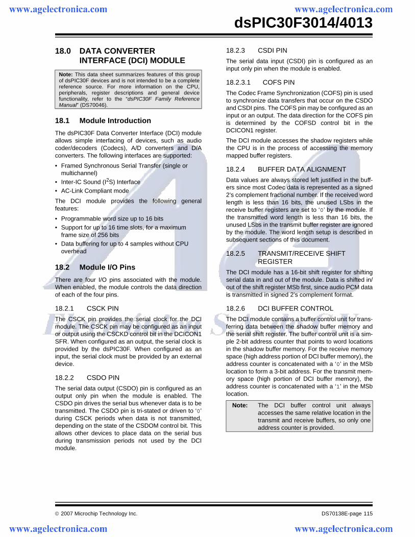
© 2007 Microchip Technology Inc. DS70138E-page 115
dsPIC30F3014/4013
18.0 DATA CONVERTER INTERFACE (DCI) MODULE
18.1 Module Introduction
The dsPIC30F Data Converter Interface (DCI) moduleallows simple interfacing of devices, such as audiocoder/decoders (Codecs), A/D converters and D/Aconverters. The following interfaces are supported:
• Framed Synchronous Serial Transfer (single or multichannel)
• Inter-IC Sound (I2S) Interface• AC-Link Compliant mode
The DCI module provides the following generalfeatures:
• Programmable word size up to 16 bits• Support for up to 16 time slots, for a maximum
frame size of 256 bits• Data buffering for up to 4 samples without CPU
overhead
18.2 Module I/O Pins
There are four I/O pins associated with the module.When enabled, the module controls the data directionof each of the four pins.
18.2.1 CSCK PIN
The CSCK pin provides the serial clock for the DCImodule. The CSCK pin may be configured as an inputor output using the CSCKD control bit in the DCICON1SFR. When configured as an output, the serial clock isprovided by the dsPIC30F. When configured as aninput, the serial clock must be provided by an externaldevice.
18.2.2 CSDO PIN
The serial data output (CSDO) pin is configured as anoutput only pin when the module is enabled. TheCSDO pin drives the serial bus whenever data is to betransmitted. The CSDO pin is tri-stated or driven to ‘0’during CSCK periods when data is not transmitted,depending on the state of the CSDOM control bit. Thisallows other devices to place data on the serial busduring transmission periods not used by the DCImodule.
18.2.3 CSDI PIN
The serial data input (CSDI) pin is configured as aninput only pin when the module is enabled.
18.2.3.1 COFS PIN
The Codec Frame Synchronization (COFS) pin is usedto synchronize data transfers that occur on the CSDOand CSDI pins. The COFS pin may be configured as aninput or an output. The data direction for the COFS pinis determined by the COFSD control bit in theDCICON1 register.
The DCI module accesses the shadow registers whilethe CPU is in the process of accessing the memorymapped buffer registers.
18.2.4 BUFFER DATA ALIGNMENT
Data values are always stored left justified in the buff-ers since most Codec data is represented as a signed2’s complement fractional number. If the received wordlength is less than 16 bits, the unused LSbs in thereceive buffer registers are set to ‘0’ by the module. Ifthe transmitted word length is less than 16 bits, theunused LSbs in the transmit buffer register are ignoredby the module. The word length setup is described insubsequent sections of this document.
18.2.5 TRANSMIT/RECEIVE SHIFT REGISTER
The DCI module has a 16-bit shift register for shiftingserial data in and out of the module. Data is shifted in/out of the shift register MSb first, since audio PCM datais transmitted in signed 2’s complement format.
18.2.6 DCI BUFFER CONTROL
The DCI module contains a buffer control unit for trans-ferring data between the shadow buffer memory andthe serial shift register. The buffer control unit is a sim-ple 2-bit address counter that points to word locationsin the shadow buffer memory. For the receive memoryspace (high address portion of DCI buffer memory), theaddress counter is concatenated with a ‘0’ in the MSblocation to form a 3-bit address. For the transmit mem-ory space (high portion of DCI buffer memory), theaddress counter is concatenated with a ‘1’ in the MSblocation.
Note: This data sheet summarizes features of this groupof dsPIC30F devices and is not intended to be a completereference source. For more information on the CPU,peripherals, register descriptions and general devicefunctionality, refer to the “dsPIC30F Family ReferenceManual” (DS70046).
Note: The DCI buffer control unit alwaysaccesses the same relative location in thetransmit and receive buffers, so only oneaddress counter is provided.
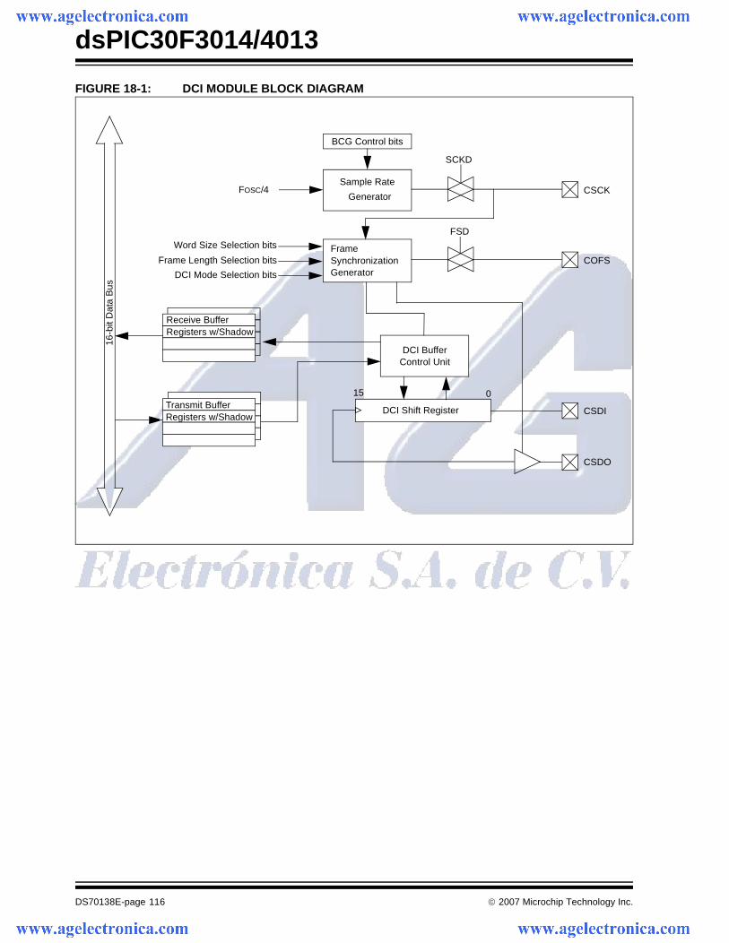
dsPIC30F3014/4013
DS70138E-page 116 © 2007 Microchip Technology Inc.
FIGURE 18-1: DCI MODULE BLOCK DIAGRAM
BCG Control bits
16-b
it D
ata
Bus
Sample Rate
Generator
SCKD
FSD
DCI Buffer
Frame SynchronizationGenerator
Control Unit
DCI Shift Register
Receive Buffer Registers w/Shadow
FOSC/4
Word Size Selection bits
Frame Length Selection bits
DCI Mode Selection bits
CSCK
COFS
CSDI
CSDO
15 0Transmit Buffer Registers w/Shadow
© 2007 Microchip Technology Inc. DS70138E-page 117
dsPIC30F3014/4013
18.3 DCI Module Operation
18.3.1 MODULE ENABLE
The DCI module is enabled or disabled by setting/clearing the DCIEN control bit in the DCICON1 SFR.Clearing the DCIEN control bit has the effect of reset-ting the module. In particular, all counters associatedwith CSCK generation, Frame Sync, and the DCI buffercontrol unit are reset.
The DCI clocks are shut down when the DCIEN bit iscleared.
When enabled, the DCI controls the data direction forthe four I/O pins associated with the module. The port,LAT and TRIS register values for these I/O pins areoverridden by the DCI module when the DCIEN bit is set.
It is also possible to override the CSCK pin separatelywhen the bit clock generator is enabled. This permitsthe bit clock generator to operate without enabling therest of the DCI module.
18.3.2 WORD-SIZE SELECTION BITS
The WS<3:0> word-size selection bits in the DCICON2SFR determine the number of bits in each DCI dataword. Essentially, the WS<3:0> bits determine thecounting period for a 4-bit counter clocked from theCSCK signal.
Any data length, up to 16 bits, may be selected. Thevalue loaded into the WS<3:0> bits is one less thedesired word length. For example, a 16-bit data wordsize is selected when WS<3:0> = 1111.
18.3.3 FRAME SYNC GENERATOR
The Frame Sync generator (COFSG) is a 4-bit counterthat sets the frame length in data words. The FrameSync generator is incremented each time the word-sizecounter is reset (refer to Section 18.3.2 “Word-SizeSelection Bits”). The period for the Frame Synchroni-zation generator is set by writing the COFSG<3:0>control bits in the DCICON2 SFR. The COFSG periodin clock cycles is determined by the following formula:
EQUATION 18-1: COFSG PERIOD
Frame lengths, up to 16 data words, may be selected.The frame length in CSCK periods can vary up to amaximum of 256 depending on the word size that isselected.
18.3.4 FRAME SYNC MODE CONTROL BITS
The type of Frame Sync signal is selected using theFrame Synchronization mode control bits(COFSM<1:0>) in the DCICON1 SFR. The followingoperating modes can be selected:
• Multichannel mode
• I2S mode• AC-Link mode (16-bit)• AC-Link mode (20-bit)
The operation of the COFSM control bits depends onwhether the DCI module generates the Frame Syncsignal as a master device, or receives the Frame Syncsignal as a slave device.
The master device in a DSP/Codec pair is the devicethat generates the Frame Sync signal. The Frame Syncsignal initiates data transfers on the CSDI and CSDOpins and usually has the same frequency as the datasample rate (COFS).
The DCI module is a Frame Sync master if the COFSDcontrol bit is cleared and is a Frame Sync slave if theCOFSD control bit is set.
18.3.5 MASTER FRAME SYNC OPERATION
When the DCI module is operating as a Frame Syncmaster device (COFSD = 0), the COFSM mode bitsdetermine the type of Frame Sync pulse that isgenerated by the Frame Sync generator logic.
A new COFS signal is generated when the Frame Syncgenerator resets to ‘0’.
In the Multichannel mode, the Frame Sync pulse isdriven high for the CSCK period to initiate a data trans-fer. The number of CSCK cycles between successiveFrame Sync pulses depends on the word size andFrame Sync generator control bits. A timing diagram forthe Frame Sync signal in Multichannel mode is shownin Figure 18-2.
In the AC-Link mode of operation, the Frame Syncsignal has a fixed period and duty cycle. The AC-LinkFrame Sync signal is high for 16 CSCK cycles and islow for 240 CSCK cycles. A timing diagram with thetiming details at the start of an AC-Link frame is shownin Figure 18-3.
In the I2S mode, a Frame Sync signal having a 50%duty cycle is generated. The period of the I2S FrameSync signal in CSCK cycles is determined by the wordsize and Frame Sync generator control bits. A new I2Sdata transfer boundary is marked by a high-to-low or alow-to-high transition edge on the COFS pin.
Note: These WS<3:0> control bits are used onlyin the Multichannel and I2S modes. Thesebits have no effect in AC-Link mode sincethe data slot sizes are fixed by the protocol.
Note: The COFSG control bits have no effect inAC-Link mode since the frame length isset to 256 CSCK periods by the protocol.
Frame Length = Word Length • (FSG Value + 1)
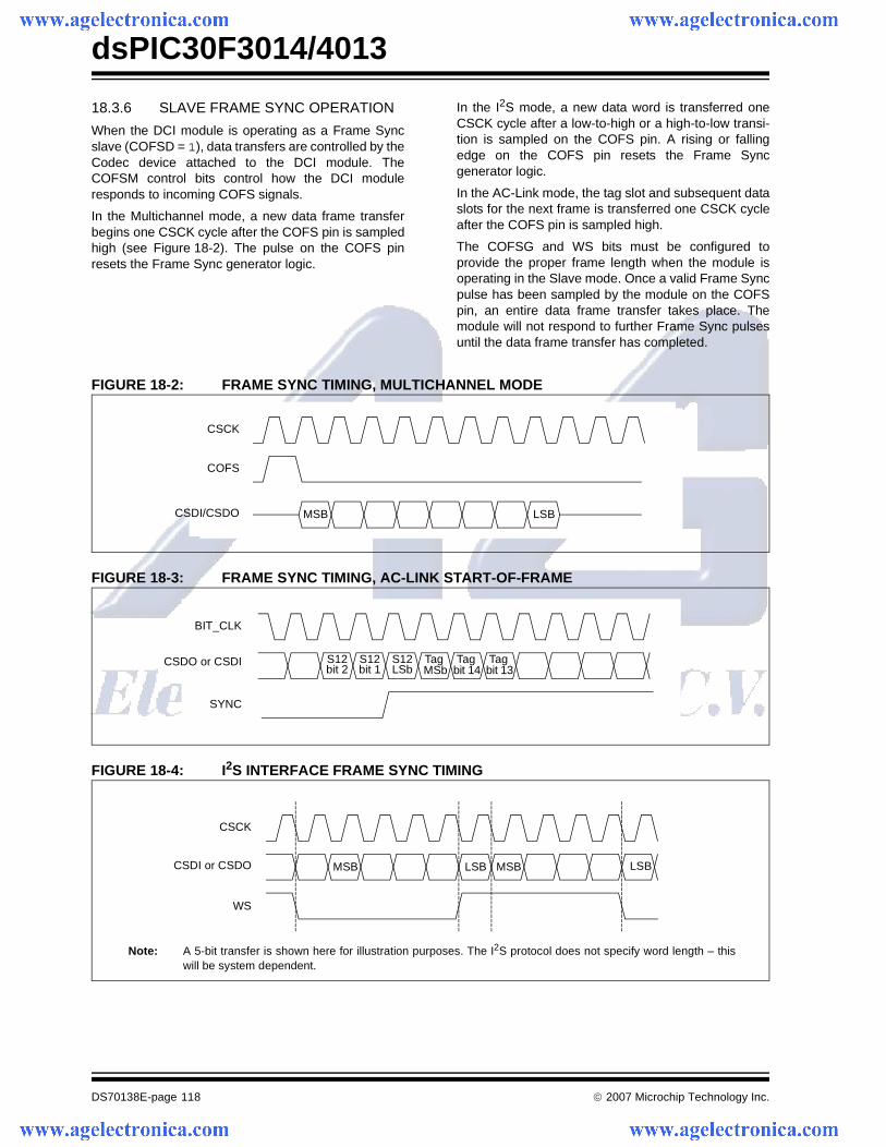
dsPIC30F3014/4013
DS70138E-page 118 © 2007 Microchip Technology Inc.
18.3.6 SLAVE FRAME SYNC OPERATION
When the DCI module is operating as a Frame Syncslave (COFSD = 1), data transfers are controlled by theCodec device attached to the DCI module. TheCOFSM control bits control how the DCI moduleresponds to incoming COFS signals.
In the Multichannel mode, a new data frame transferbegins one CSCK cycle after the COFS pin is sampledhigh (see Figure 18-2). The pulse on the COFS pinresets the Frame Sync generator logic.
In the I2S mode, a new data word is transferred oneCSCK cycle after a low-to-high or a high-to-low transi-tion is sampled on the COFS pin. A rising or fallingedge on the COFS pin resets the Frame Syncgenerator logic.
In the AC-Link mode, the tag slot and subsequent dataslots for the next frame is transferred one CSCK cycleafter the COFS pin is sampled high.
The COFSG and WS bits must be configured toprovide the proper frame length when the module isoperating in the Slave mode. Once a valid Frame Syncpulse has been sampled by the module on the COFSpin, an entire data frame transfer takes place. Themodule will not respond to further Frame Sync pulsesuntil the data frame transfer has completed.
FIGURE 18-2: FRAME SYNC TIMING, MULTICHANNEL MODE
FIGURE 18-3: FRAME SYNC TIMING, AC-LINK START-OF-FRAME
FIGURE 18-4: I2S INTERFACE FRAME SYNC TIMING
CSCK
CSDI/CSDO
COFS
MSB LSB
TagMSb
BIT_CLK
CSDO or CSDI
SYNC
Tagbit 14
S12LSb
S12bit 1
S12bit 2
Tagbit 13
MSB LSB MSB LSB
CSCK
CSDI or CSDO
WS
Note: A 5-bit transfer is shown here for illustration purposes. The I2S protocol does not specify word length – thiswill be system dependent.
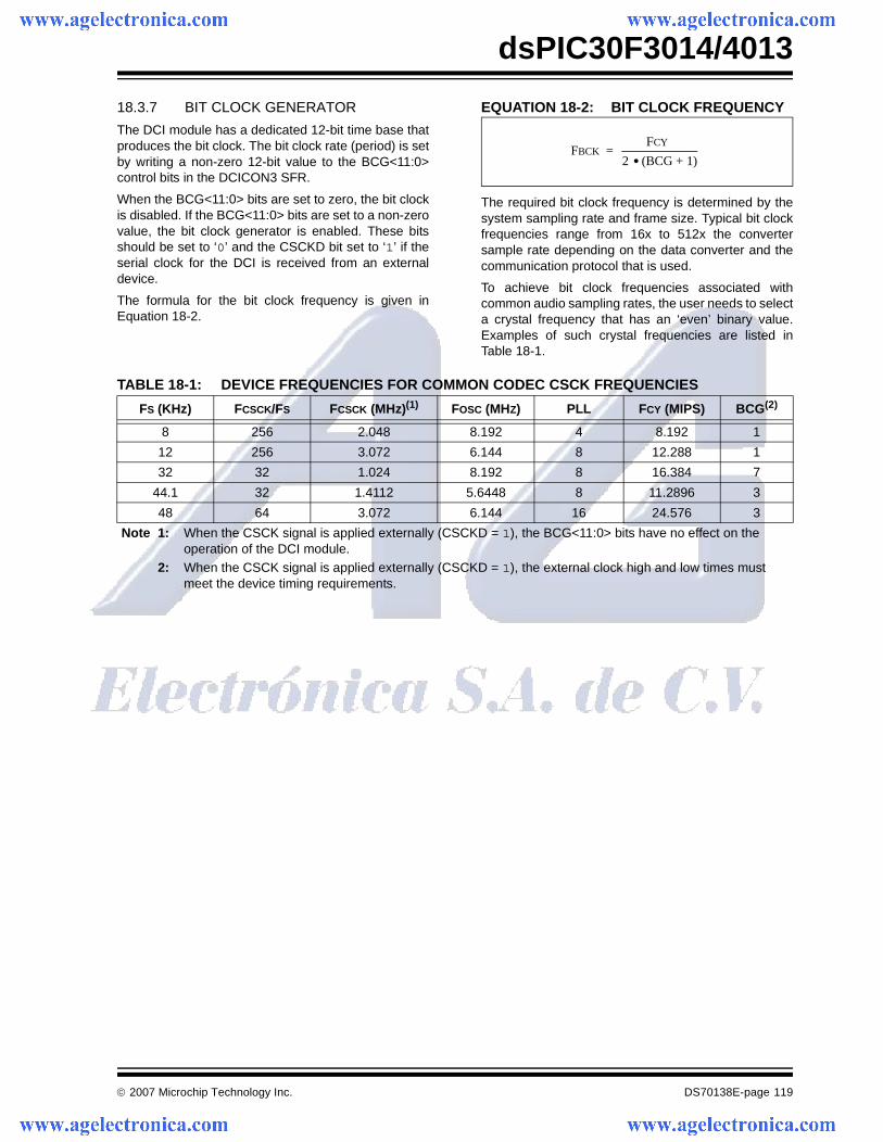
© 2007 Microchip Technology Inc. DS70138E-page 119
dsPIC30F3014/4013
18.3.7 BIT CLOCK GENERATOR
The DCI module has a dedicated 12-bit time base thatproduces the bit clock. The bit clock rate (period) is setby writing a non-zero 12-bit value to the BCG<11:0>control bits in the DCICON3 SFR.
When the BCG<11:0> bits are set to zero, the bit clockis disabled. If the BCG<11:0> bits are set to a non-zerovalue, the bit clock generator is enabled. These bitsshould be set to ‘0’ and the CSCKD bit set to ‘1’ if theserial clock for the DCI is received from an externaldevice.
The formula for the bit clock frequency is given inEquation 18-2.
EQUATION 18-2: BIT CLOCK FREQUENCY
The required bit clock frequency is determined by thesystem sampling rate and frame size. Typical bit clockfrequencies range from 16x to 512x the convertersample rate depending on the data converter and thecommunication protocol that is used.
To achieve bit clock frequencies associated withcommon audio sampling rates, the user needs to selecta crystal frequency that has an ‘even’ binary value.Examples of such crystal frequencies are listed inTable 18-1.
TABLE 18-1: DEVICE FREQUENCIES FOR COMMON CODEC CSCK FREQUENCIES
FBCK =FCY
2 (BCG + 1)•
FS (KHz) FCSCK/FS FCSCK (MHz)(1) FOSC (MHZ) PLL FCY (MIPS) BCG(2)
8 256 2.048 8.192 4 8.192 1
12 256 3.072 6.144 8 12.288 1
32 32 1.024 8.192 8 16.384 7
44.1 32 1.4112 5.6448 8 11.2896 3
48 64 3.072 6.144 16 24.576 3
Note 1: When the CSCK signal is applied externally (CSCKD = 1), the BCG<11:0> bits have no effect on the operation of the DCI module.
2: When the CSCK signal is applied externally (CSCKD = 1), the external clock high and low times must meet the device timing requirements.
dsPIC30F3014/4013
DS70138E-page 120 © 2007 Microchip Technology Inc.
18.3.8 SAMPLE CLOCK EDGE CONTROL BIT
The sample clock edge (CSCKE) control bit determinesthe sampling edge for the CSCK signal. If the CSCK bitis cleared (default), data is sampled on the falling edgeof the CSCK signal. The AC-Link protocols and mostmultichannel formats require that data be sampled onthe falling edge of the CSCK signal. If the CSCK bit isset, data is sampled on the rising edge of CSCK. TheI2S protocol requires that data be sampled on the risingedge of the CSCK signal.
18.3.9 DATA JUSTIFICATION CONTROL BIT
In most applications, the data transfer begins oneCSCK cycle after the COFS signal is sampled active.This is the default configuration of the DCI module. Analternate data alignment can be selected by setting theDJST control bit in the DCICON1 SFR. When DJST = 1,data transfers begin during the same CSCK cycle whenthe COFS signal is sampled active.
18.3.10 TRANSMIT SLOT ENABLE BITS
The TSCON SFR has control bits that are used toenable up to 16 time slots for transmission. These con-trol bits are the TSE<15:0> bits. The size of each timeslot is determined by the WS<3:0> word-size selectionbits and can vary up to 16 bits.
If a transmit time slot is enabled via one of the TSE bits(TSEx = 1), the contents of the current transmit shadowbuffer location is loaded into the CSDO Shift registerand the DCI buffer control unit is incremented to pointto the next location.
During an unused transmit time slot, the CSDO pindrives ‘0’s or is tri-stated during all disabled time slotsdepending on the state of the CSDOM bit in theDCICON1 SFR.
The data frame size in bits is determined by the chosendata word size and the number of data word elementsin the frame. If the chosen frame size has less than 16elements, the additional slot enable bits have no effect.
Each transmit data word is written to the 16-bit transmitbuffer as left justified data. If the selected word size isless than 16 bits, then the LSbs of the transmit buffermemory have no effect on the transmitted data. Theuser should write ‘0’s to the unused LSbs of each trans-mit buffer location.
18.3.11 RECEIVE SLOT ENABLE BITS
The RSCON SFR contains control bits that are used toenable up to 16 time slots for reception. These controlbits are the RSE<15:0> bits. The size of each receivetime slot is determined by the WS<3:0> word-sizeselection bits and can vary from 1 to 16 bits.
If a receive time slot is enabled via one of the RSE bits(RSEx = 1), the shift register contents are written to thecurrent DCI receive shadow buffer location and thebuffer control unit is incremented to point to the nextbuffer location.
Data is not packed in the receive memory buffer loca-tions if the selected word size is less than 16 bits. Eachreceived slot data word is stored in a separate 16-bitbuffer location. Data is always stored in a left justifiedformat in the receive memory buffer.
18.3.12 SLOT ENABLE BITS OPERATION WITH FRAME SYNC
The TSE and RSE control bits operate in concert withthe DCI Frame Sync generator. In the Master mode, aCOFS signal is generated whenever the Frame Syncgenerator is reset. In the Slave mode, the Frame Syncgenerator is reset whenever a COFS pulse is received.
The TSE and RSE control bits allow up to 16 consecu-tive time slots to be enabled for transmit or receive.After the last enabled time slot has been transmitted/received, the DCI stops buffering data until the nextoccurring COFS pulse.
18.3.13 SYNCHRONOUS DATA TRANSFERS
The DCI buffer control unit is incremented by one wordlocation whenever a given time slot has been enabledfor transmission or reception. In most cases, data inputand output transfers are synchronized, which meansthat a data sample is received for a given channel at thesame time a data sample is transmitted. Therefore, thetransmit and receive buffers are filled with equalamounts of data when a DCI interrupt is generated.
In some cases, the amount of data transmitted andreceived during a data frame may not be equal. As anexample, assume a two-word data frame is used.Furthermore, assume that data is only received duringslot #0 but is transmitted during slot #0 and slot #1. Inthis case, the buffer control unit counter would beincremented twice during a data frame but only onereceive register location would be filled with data.
© 2007 Microchip Technology Inc. DS70138E-page 121
dsPIC30F3014/4013
18.3.14 BUFFER LENGTH CONTROL
The amount of data that is buffered between interruptsis determined by the buffer length (BLEN<1:0>) controlbits in the DCICON2 SFR. The size of the transmit andreceive buffers may be varied from 1 to 4 data wordsusing the BLEN control bits. The BLEN control bits arecompared to the current value of the DCI buffer controlunit address counter. When the two LSbs of the DCIaddress counter match the BLEN<1:0> value, thebuffer control unit is reset to ‘0’. In addition, the con-tents of the receive shadow registers are transferred tothe receive buffer registers and the contents of thetransmit buffer registers are transferred to the transmitshadow registers.
18.3.15 BUFFER ALIGNMENT WITH DATA FRAMES
There is no direct coupling between the position of theAGU Address Pointer and the data frame boundaries.This means that there is an implied assignment of eachtransmit and receive buffer that is a function of theBLEN control bits and the number of enabled data slotsvia the TSE and RSE control bits.
As an example, assume that a 4-word data frame ischosen and that we want to transmit on all four timeslots in the frame. This configuration would be estab-lished by setting the TSE0, TSE1, TSE2, and TSE3control bits in the TSCON SFR. With this module setup,the TXBUF0 register would be naturally assigned toslot #0, the TXBUF1 register would be naturallyassigned to slot #1, and so on.
18.3.16 TRANSMIT STATUS BITS
There are two transmit Status bits in the DCISTAT SFR.
The TMPTY bit is set when the contents of the transmitbuffer registers are transferred to the transmit shadowregisters. The TMPTY bit may be polled in software todetermine when the transmit buffer registers may bewritten. The TMPTY bit is cleared automatically by thehardware when a write to one of the four transmitbuffers occurs.
The TUNF bit is read-only and indicates that a transmitunderflow has occurred for at least one of the transmitbuffer registers that is in use. The TUNF bit is set at thetime the transmit buffer registers are transferred to thetransmit shadow registers. The TUNF Status bit iscleared automatically when the buffer register thatunderflowed is written by the CPU.
18.3.17 RECEIVE STATUS BITS
There are two receive Status bits in the DCISTAT SFR.
The RFUL Status bit is read-only and indicates thatnew data is available in the receive buffers. The RFULbit is cleared automatically when all receive buffers inuse have been read by the CPU.
The ROV Status bit is read-only and indicates that areceive overflow has occurred for at least one of thereceive buffer locations. A receive overflow occurswhen the buffer location is not read by the CPU beforenew data is transferred from the shadow registers. TheROV Status bit is cleared automatically when the bufferregister that caused the overflow is read by the CPU.
When a receive overflow occurs for a specific bufferlocation, the old contents of the buffer are overwritten.
Note: When more than four time slots are activewithin a data frame, the user code mustkeep track of which time slots are to beread/written at each interrupt. In somecases, the alignment between transmit/receive buffers and their respective slotassignments could be lost. Examples ofsuch cases include an emulation break-point or a hardware trap. In these situa-tions, the user should poll the SLOT Statusbits to determine what data should beloaded into the buffer registers toresynchronize the software with the DCImodule.
Note: The transmit Status bits only indicate sta-tus for buffer locations that are used by themodule. If the buffer length is set to lessthan four words, for example, the unusedbuffer locations do not affect the transmitStatus bits.
Note: The receive Status bits only indicate statusfor buffer locations that are used by themodule. If the buffer length is set to lessthan four words, for example, the unusedbuffer locations do not affect the transmitStatus bits.
dsPIC30F3014/4013
DS70138E-page 122 © 2007 Microchip Technology Inc.
18.3.18 SLOT STATUS BITS
The SLOT<3:0> Status bits in the DCISTAT SFR indi-cate the current active time slot. These bits correspondto the value of the Frame Sync generator counter. Theuser may poll these Status bits in software when a DCIinterrupt occurs to determine what time slot data waslast received and which time slot data should be loadedinto the TXBUF registers.
18.3.19 CSDO MODE BIT
The CSDOM control bit controls the behavior of theCSDO pin during unused transmit slots. A given trans-mit time slot is unused if it’s corresponding TSEx bit inthe TSCON SFR is cleared.
If the CSDOM bit is cleared (default), the CSDO pin islow during unused time slot periods. This mode is usedwhen there are only two devices attached to the serialbus.
If the CSDOM bit is set, the CSDO pin is tri-stated dur-ing unused time slot periods. This mode allows multipledevices to share the same CSDO line in a multichannelapplication. Each device on the CSDO line is config-ured so that it only transmits data during specific timeslots. No two devices transmit data during the sametime slot.
18.3.20 DIGITAL LOOPBACK MODE
Digital Loopback mode is enabled by setting theDLOOP control bit in the DCICON1 SFR. When theDLOOP bit is set, the module internally connects theCSDO signal to CSDI. The actual data input on theCSDI I/O pin is ignored in Digital Loopback mode.
18.3.21 UNDERFLOW MODE CONTROL BIT
When an underflow occurs, one of two actions mayoccur depending on the state of the Underflow mode(UNFM) control bit in the DCICON1 SFR. If the UNFMbit is cleared (default), the module transmits ‘0’s on theCSDO pin during the active time slot for the buffer loca-tion. In this operating mode, the Codec device attachedto the DCI module is simply fed digital ‘silence’. If theUNFM control bit is set, the module transmits the lastdata written to the buffer location. This operating modepermits the user to send continuous data to the Codecdevice without consuming CPU overhead.
18.4 DCI Module Interrupts
The frequency of DCI module interrupts is dependenton the BLEN<1:0> control bits in the DCICON2 SFR.An interrupt to the CPU is generated each time the setbuffer length has been reached and a shadow registertransfer takes place. A shadow register transfer isdefined as the time when the previously written TXBUFvalues are transferred to the transmit shadow registersand new received values in the receive shadowregisters are transferred into the RXBUF registers.
18.5 DCI Module Operation During CPU Sleep and Idle Modes
18.5.1 DCI MODULE OPERATION DURING CPU SLEEP MODE
The DCI module has the ability to operate while inSleep mode and wake the CPU when the CSCK signalis supplied by an external device (CSCKD = 1). TheDCI module generates an asynchronous interruptwhen a DCI buffer transfer has completed and the CPUis in Sleep mode.
18.5.2 DCI MODULE OPERATION DURING CPU IDLE MODE
If the DCISIDL control bit is cleared (default), the mod-ule continues to operate normally even in Idle mode. Ifthe DCISIDL bit is set, the module halts when Idlemode is asserted.
18.6 AC-Link Mode Operation
The AC-Link protocol is a 256-bit frame with one 16-bitdata slot, followed by twelve 20-bit data slots. The DCImodule has two operating modes for the AC-Link pro-tocol. These operating modes are selected by theCOFSM<1:0> control bits in the DCICON1 SFR. Thefirst AC-Link mode is called ‘16-bit AC-Link mode’ andis selected by setting COFSM<1:0> = 10. The secondAC-Link mode is called ‘20-bit AC-Link mode’ and isselected by setting COFSM<1:0> = 11.
18.6.1 16-BIT AC-LINK MODE
In the 16-bit AC-Link mode, data word lengths arerestricted to 16 bits. Note that this restriction onlyaffects the 20-bit data time slots of the AC-Link proto-col. For received time slots, the incoming data is simplytruncated to 16 bits. For outgoing time slots, the 4 LSbsof the data word are set to ‘0’ by the module. This trun-cation of the time slots limits the A/D and DAC data to16 bits but permits proper data alignment in the TXBUFand RXBUF registers. Each RXBUF and TXBUFregister contains one data time slot value.
© 2007 Microchip Technology Inc. DS70138E-page 123
dsPIC30F3014/4013
18.6.2 20-BIT AC-LINK MODE
The 20-bit AC-Link mode allows all bits in the data timeslots to be transmitted and received but does not main-tain data alignment in the TXBUF and RXBUFregisters.
The 20-bit AC-Link mode functions similar to the Multi-channel mode of the DCI module, except for the dutycycle of the Frame Synchronization signal. The AC-Link Frame Synchronization signal should remain highfor 16 CSCK cycles and should be low for the following240 cycles.
The 20-bit mode treats each 256-bit AC-Link frame assixteen, 16-bit time slots. In the 20-bit AC-Link mode,the module operates as if COFSG<3:0> = 1111 andWS<3:0> = 1111. The data alignment for 20-bit dataslots is ignored. For example, an entire AC-Link dataframe can be transmitted and received in a packedfashion by setting all bits in the TSCON and RSCONSFRs. Since the total available buffer length is 64 bits,it would take 4 consecutive interrupts to transfer theAC-Link frame. The application software must keeptrack of the current AC-Link frame segment.
18.7 I2S Mode Operation
The DCI module is configured for I2S mode by writinga value of ‘01’ to the COFSM<1:0> control bits in theDCICON1 SFR. When operating in the I2S mode, theDCI module generates Frame Synchronization signalswith a 50% duty cycle. Each edge of the FrameSynchronization signal marks the boundary of a newdata word transfer.
The user must also select the frame length and dataword size using the COFSG and WS control bits in theDCICON2 SFR.
18.7.1 I2S FRAME AND DATA WORD LENGTH SELECTION
The WS and COFSG control bits are set to produce theperiod for one half of an I2S data frame. That is, theframe length is the total number of CSCK cyclesrequired for a left or a right data word transfer.
The BLEN bits must be set for the desired buffer length.Setting BLEN<1:0> = 01 produces a CPU interrupt,once per I2S frame.
18.7.2 I2S DATA JUSTIFICATION
As per the I2S specification, a data word transfer, bydefault, begins one CSCK cycle after a transition of theWS signal. A ‘MSb left justified’ option can be selectedusing the DJST control bit in the DCICON1 SFR.
If DJST = 1, the I2S data transfers are MSb left justified.The MSb of the data word is presented on the CSDOpin during the same CSCK cycle as the rising or fallingedge of the COFS signal. The CSDO pin is tri-statedafter the data word has been sent.
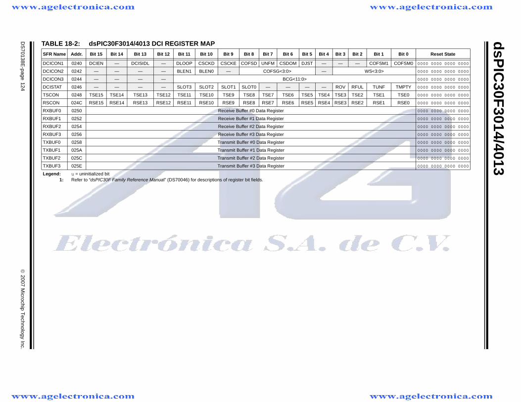
dsP
IC30F
3014/4013
DS
70138E-page 124
© 2007 M
icrochip Technology Inc.
TABLE 18-2: dsPIC30F3014/4013 DCI REGISTER MAP
SFR Name Addr. Bit 15 Bit 14 Bit 13 Bit 12 Bit 11 Bit 10 Bit 9 Bit 8 Bit 7 Bit 6 Bit 5 Bit 4 Bit 3 Bit 2 Bit 1 Bit 0 Reset State
DCICON1 0240 DCIEN — DCISIDL — DLOOP CSCKD CSCKE COFSD UNFM CSDOM DJST — — — COFSM1 COFSM0 0000 0000 0000 0000
DCICON2 0242 — — — — BLEN1 BLEN0 — COFSG<3:0> — WS<3:0> 0000 0000 0000 0000
DCICON3 0244 — — — — BCG<11:0> 0000 0000 0000 0000
DCISTAT 0246 — — — — SLOT3 SLOT2 SLOT1 SLOT0 — — — — ROV RFUL TUNF TMPTY 0000 0000 0000 0000
TSCON 0248 TSE15 TSE14 TSE13 TSE12 TSE11 TSE10 TSE9 TSE8 TSE7 TSE6 TSE5 TSE4 TSE3 TSE2 TSE1 TSE0 0000 0000 0000 0000
RSCON 024C RSE15 RSE14 RSE13 RSE12 RSE11 RSE10 RSE9 RSE8 RSE7 RSE6 RSE5 RSE4 RSE3 RSE2 RSE1 RSE0 0000 0000 0000 0000
RXBUF0 0250 Receive Buffer #0 Data Register 0000 0000 0000 0000
RXBUF1 0252 Receive Buffer #1 Data Register 0000 0000 0000 0000
RXBUF2 0254 Receive Buffer #2 Data Register 0000 0000 0000 0000
RXBUF3 0256 Receive Buffer #3 Data Register 0000 0000 0000 0000
TXBUF0 0258 Transmit Buffer #0 Data Register 0000 0000 0000 0000
TXBUF1 025A Transmit Buffer #1 Data Register 0000 0000 0000 0000
TXBUF2 025C Transmit Buffer #2 Data Register 0000 0000 0000 0000
TXBUF3 025E Transmit Buffer #3 Data Register 0000 0000 0000 0000
Legend: u = uninitialized bit1: Refer to “dsPIC30F Family Reference Manual” (DS70046) for descriptions of register bit fields.
© 2007 Microchip Technology Inc. DS70138E-page 125
dsPIC30F3014/4013
19.0 12-BIT ANALOG-TO-DIGITAL CONVERTER (ADC) MODULE
The 12-bit Analog-to-Digital Converter (ADC) allowsconversion of an analog input signal to a 12-bit digitalnumber. This module is based on a SuccessiveApproximation Register (SAR) architecture and pro-vides a maximum sampling rate of 200 ksps. The A/Dmodule has up to 16 analog inputs which are multi-plexed into a sample and hold amplifier. The output ofthe sample and hold is the input into the converterwhich generates the result. The analog reference volt-age is software selectable to either the device supplyvoltage (AVDD/AVSS) or the voltage level on the(VREF+/VREF-) pin. The A/D converter has a uniquefeature of being able to operate while the device is inSleep mode with RC oscillator selection.
The A/D module has six 16-bit registers:
• A/D Control Register 1 (ADCON1)• A/D Control Register 2 (ADCON2)
• A/D Control Register 3 (ADCON3)• A/D Input Select Register (ADCHS)• A/D Port Configuration Register (ADPCFG)
• A/D Input Scan Selection Register (ADCSSL)
The ADCON1, ADCON2 and ADCON3 registerscontrol the operation of the A/D module. The ADCHSregister selects the input channels to be converted. TheADPCFG register configures the port pins as analoginputs or as digital I/O. The ADCSSL register selectsinputs for scanning.
The block diagram of the 12-bit A/D module is shown inFigure 19-1.
FIGURE 19-1: 12-BIT A/D FUNCTIONAL BLOCK DIAGRAM
Note: This data sheet summarizes features of this groupof dsPIC30F devices and is not intended to be a completereference source. For more information on the CPU,peripherals, register descriptions and general devicefunctionality, refer to the “dsPIC30F Family ReferenceManual” (DS70046).
Note: The SSRC<2:0>, ASAM, SMPI<3:0>,BUFM and ALTS bits, as well as theADCON3 and ADCSSL registers, mustnot be written to while ADON = 1. Thiswould lead to indeterminate results.
Comparator
12-bit SAR Conversion Logic
VREF+
DAC
Dat
a
16-word, 12-bitDual Port
RAM
Bus
Inte
rfac
e
AN12
0000
0101
0111
1001
1100
0001
0010
0011
0100
0110
1000
1010
1011
AN8
AN9
AN10
AN11
AN4
AN5
AN6
AN7
AN0
AN1
AN2
AN3
CH0
AN1VREF-
VREF-
Sample/SequenceControlSample
Input MUXControl
InputSwitches
S/H
AVSS
AVDD
For
mat
Note: The ADCHS, ADPCFG and ADCSSL registers allow the application to configure AN13-AN15 as analog input pins.Since these pins are not physically present on the device, conversion results from these pins will read ‘0’.
dsPIC30F3014/4013
DS70138E-page 126 © 2007 Microchip Technology Inc.
19.1 A/D Result Buffer
The module contains a 16-word dual port read-onlybuffer, called ADCBUF0...ADCBUFF, to buffer the A/Dresults. The RAM is 12 bits wide but the data obtainedis represented in one of four different 16-bit data for-mats. The contents of the sixteen A/D ConversionResult Buffer registers, ADCBUF0 through ADCBUFF,cannot be written by user software.
19.2 Conversion Operation
After the A/D module has been configured, the sampleacquisition is started by setting the SAMP bit. Varioussources, such as a programmable bit, timer time-outsand external events, terminate acquisition and start aconversion. When the A/D conversion is complete, theresult is loaded into ADCBUF0...ADCBUFF, and theDONE bit and the A/D interrupt flag, ADIF, are set afterthe number of samples specified by the SMPI bit. TheADC module can be configured for different interruptrates as described in Section 19.3 “Selecting theConversion Sequence”.
The following steps should be followed for doing anA/D conversion:
1. Configure the A/D module:• Configure analog pins, voltage reference and
digital I/O• Select A/D input channels• Select A/D conversion clock
• Select A/D conversion trigger• Turn on A/D module
2. Configure A/D interrupt (if required):
• Clear ADIF bit • Select A/D interrupt priority• Set ADIE bit (for ISR processing)
3. Start sampling4. Wait the required acquisition time5. Trigger acquisition end, start conversion:
6. Wait for A/D conversion to complete, by either:• Waiting for the A/D interrupt, or• Waiting for the DONE bit to get set.
7. Read A/D result buffer, clear ADIF if required
19.3 Selecting the Conversion Sequence
Several groups of control bits select the sequence inwhich the A/D connects inputs to the sample/holdchannel, converts a channel, writes the buffer memoryand generates interrupts.
The sequence is controlled by the sampling clocks.
The SMPI bits select the number of acquisition/conversion sequences that would be performed beforean interrupt occurs. This can vary from 1 sample perinterrupt to 16 samples per interrupt.
The BUFM bit splits the 16-word results buffer into two8-word groups. Writing to the 8-word buffers is alter-nated on each interrupt event.
Use of the BUFM bit depends on how much time isavailable for moving the buffers after the interrupt.
If the processor can quickly unload a full buffer withinthe time it takes to acquire and convert one channel,the BUFM bit can be ‘0’ and up to 16 conversions (cor-responding to the 16 input channels) may be done perinterrupt. The processor has one acquisition andconversion time to move the sixteen conversions.
If the processor cannot unload the buffer within theacquisition and conversion time, the BUFM bit should be‘1’. For example, if SMPI<3:0> (ADCON2<5:2>) = 0111,then eight conversions are loaded into 1/2 of the buffer,following which an interrupt occurs. The next eight con-versions are loaded into the other 1/2 of the buffer. Theprocessor has the entire time between interrupts tomove the eight conversions.
The ALTS bit can be used to alternate the inputsselected during the sampling sequence. The inputmultiplexer has two sets of sample inputs: MUX A andMUX B. If the ALTS bit is ‘0’, only the MUX A inputs areselected for sampling. If the ALTS bit is ‘1’ andSMPI<3:0> = 0000 on the first sample/convertsequence, the MUX A inputs are selected and on thenext acquire/convert sequence, the MUX B inputs areselected.
The CSCNA bit (ADCON2<10>) allows the S/H input tobe sequentially scanned across a selected number ofanalog inputs for the MUX A group. The inputs areselected by the ADCSSL register. If a particular bit inthe ADCSSL register is ‘1’, the corresponding input isselected. The inputs are always scanned from lower tohigher numbered inputs, starting after each interrupt. Ifthe number of inputs selected is greater than thenumber of samples taken per interrupt, the highernumbered inputs are unused.
Note: The ADCHS, ADPCFG and ADCSSL reg-isters allow the application to configureAN13-AN15 as analog input pins. Sincethese pins are not physically present onthe device, conversion results from thesepins read ‘0’.
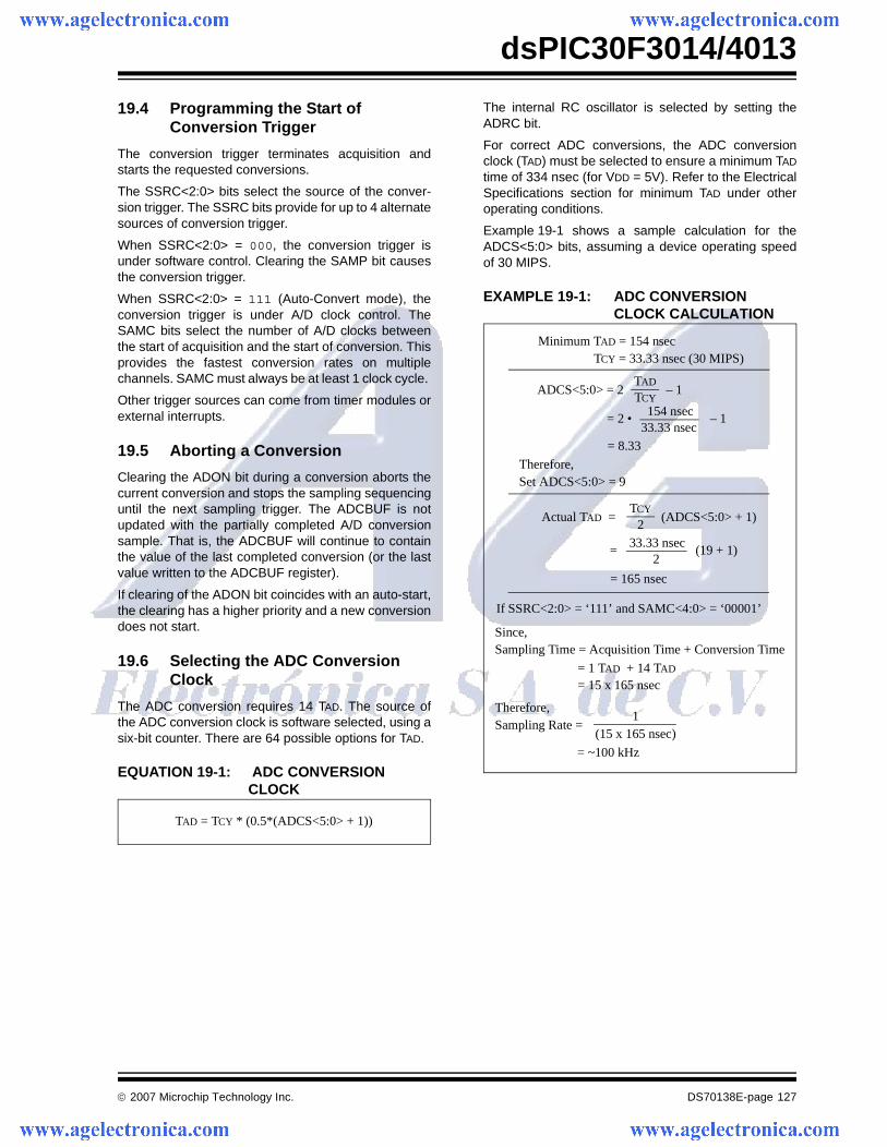
© 2007 Microchip Technology Inc. DS70138E-page 127
dsPIC30F3014/4013
19.4 Programming the Start of Conversion Trigger
The conversion trigger terminates acquisition andstarts the requested conversions.
The SSRC<2:0> bits select the source of the conver-sion trigger. The SSRC bits provide for up to 4 alternatesources of conversion trigger.
When SSRC<2:0> = 000, the conversion trigger isunder software control. Clearing the SAMP bit causesthe conversion trigger.
When SSRC<2:0> = 111 (Auto-Convert mode), theconversion trigger is under A/D clock control. TheSAMC bits select the number of A/D clocks betweenthe start of acquisition and the start of conversion. Thisprovides the fastest conversion rates on multiplechannels. SAMC must always be at least 1 clock cycle.
Other trigger sources can come from timer modules orexternal interrupts.
19.5 Aborting a Conversion
Clearing the ADON bit during a conversion aborts thecurrent conversion and stops the sampling sequencinguntil the next sampling trigger. The ADCBUF is notupdated with the partially completed A/D conversionsample. That is, the ADCBUF will continue to containthe value of the last completed conversion (or the lastvalue written to the ADCBUF register).
If clearing of the ADON bit coincides with an auto-start,the clearing has a higher priority and a new conversiondoes not start.
19.6 Selecting the ADC Conversion Clock
The ADC conversion requires 14 TAD. The source ofthe ADC conversion clock is software selected, using asix-bit counter. There are 64 possible options for TAD.
EQUATION 19-1: ADC CONVERSION CLOCK
The internal RC oscillator is selected by setting theADRC bit.
For correct ADC conversions, the ADC conversionclock (TAD) must be selected to ensure a minimum TAD
time of 334 nsec (for VDD = 5V). Refer to the ElectricalSpecifications section for minimum TAD under otheroperating conditions.
Example 19-1 shows a sample calculation for theADCS<5:0> bits, assuming a device operating speedof 30 MIPS.
EXAMPLE 19-1: ADC CONVERSION CLOCK CALCULATION
TAD = TCY * (0.5*(ADCS<5:0> + 1))
Minimum TAD = 154 nsec
ADCS<5:0> = 2 – 1TAD
TCY
TCY = 33.33 nsec (30 MIPS)
= 2 • – 1154 nsec
33.33 nsec
= 8.33
Therefore,Set ADCS<5:0> = 9
Actual TAD = (ADCS<5:0> + 1)TCY
2
= (19 + 1)33.33 nsec
2
= 165 nsec
If SSRC<2:0> = ‘111’ and SAMC<4:0> = ‘00001’
Since,Sampling Time = Acquisition Time + Conversion Time
= 1 TAD + 14 TAD = 15 x 165 nsec
Therefore,Sampling Rate =
= ~100 kHz
1(15 x 165 nsec)
dsPIC30F3014/4013
DS70138E-page 128 © 2007 Microchip Technology Inc.
19.7 ADC Speeds
The dsPIC30F 12-bit ADC specifications permit amaximum of 200 ksps sampling rate. The table belowsummarizes the conversion speeds for the dsPIC30F12-bit ADC and the required operating conditions.
TABLE 19-1: 12-BIT ADC EXTENDED CONVERSION RATES
dsPIC30F 12-bit ADC Conversion Rates
SpeedTAD
MinimumSampling Time Min
Rs Max VDD Temperature Channels Configuration
Up to 200 ksps(1)
334 ns 1 TAD 2.5 kΩ 4.5V to 5.5V -40°C to +85°C
Up to 100 ksps
668 ns 1 TAD 2.5 kΩ 3.0V to 5.5V -40°C to +125°C
Note 1: External VREF- and VREF+ pins must be used for correct operation. See Figure 19-2 for recommendedcircuit.
VREF- VREF+
ADCANx
S/H
CHX
VREF- VREF+
ADCANx
S/H
CHX
ANx or VREF-
orAVSS
orAVDD
© 2007 Microchip Technology Inc. DS70138E-page 129
dsPIC30F3014/4013
The following figure depicts the recommended circuitfor the conversion rates above 200 ksps. ThedsPIC30F3014 is shown as an example.
FIGURE 19-2: ADC VOLTAGE REFERENCE SCHEMATIC
The configuration procedures below give the requiredsetup values for the conversion speeds above 100ksps.
19.7.1 200 KSPS CONFIGURATION GUIDELINE
The following configuration items are required toachieve a 200 ksps conversion rate.
• Comply with conditions provided in Table 19-2.• Connect external VREF+ and VREF- pins following
the recommended circuit shown in Figure 19-2.• Set SSRC<2.0> = 111 in the ADCON1 register to
enable the auto-convert option.• Enable automatic sampling by setting the ASAM
control bit in the ADCON1 register.• Write the SMPI<3.0> control bits in the ADCON2
register for the desired number of conversions between interrupts.
• Configure the ADC clock period to be:
by writing to the ADCS<5:0> control bits in the ADCON3 register.
• Configure the sampling time to be 1 TAD by writing: SAMC<4:0> = 00001.
The following figure shows the timing diagram of theADC running at 200 ksps. The TAD selection in conjunc-tion with the guidelines described above allows a con-version speed of 200 ksps. See Example 19-1 for codeexample.
VDD
VDD
VDD
VDD
R210
C20.1 μF
C10.01 μF
R110
C81 μF
VDD
C70.1 μF
VDD
C60.01 μF
AVDD
C51 μF
AVDD
C40.1 μF
AVDD
C30.01 μF
See Note 1:
Note 1: Ensure adequate bypass capacitors are provided on each VDD pin.
1011
2
3
4
5
6
1
18 19 20 21 2212 13 14 15
38
8
7
44 43 42 41 40 39
16 1729
30
3132
33
232425
26
27
28
36 34359
37
dsPIC30F3014
VSS
VSS
VDD
VDD
VR
EF-
VR
EF+
AV
SS
AV
DD
VSS
VDD
VDD
VDD
1
(14 + 1) x 200,000= 334 ns
dsPIC30F3014/4013
DS70138E-page 130 © 2007 Microchip Technology Inc.
FIGURE 19-3: CONVERTING 1 CHANNEL AT 200 KSPS, AUTO-SAMPLE START, 1 TAD SAMPLING TIME
19.8 A/D Acquisition Requirements
The analog input model of the 12-bit A/D converter isshown in Figure 19-4. The total sampling time for the A/D is a function of the internal amplifier settling time andthe holding capacitor charge time.
For the A/D converter to meet its specified accuracy,the charge holding capacitor (CHOLD) must be allowedto fully charge to the voltage level on the analog inputpin. The source impedance (RS), the interconnectimpedance (RIC), and the internal sampling switch(RSS) impedance combine to directly affect the time
required to charge the capacitor CHOLD. The combinedimpedance of the analog sources must therefore besmall enough to fully charge the holding capacitorwithin the chosen sample time. To minimize the effectsof pin leakage currents on the accuracy of the A/D con-verter, the maximum recommended source imped-ance, RS, is 2.5 kΩ. After the analog input channel isselected (changed), this sampling function must becompleted prior to starting the conversion. The internalholding capacitor will be in a discharged state prior toeach sample operation.
FIGURE 19-4: 12-BIT A/D CONVERTER ANALOG INPUT MODEL
TCONV= 14 TAD
TSAMP= 1 TAD
TSAMP= 1 TAD
ADCLK
SAMP
DONE
ADCBUF0
ADCBUF1
Instruction Execution BSET ADCON1, ASAM
TCONV= 14 TAD
CPINVA
Rs ANxVT = 0.6V
VT = 0.6VI leakage
RIC ≤ 250Ω SamplingSwitch
RSS
CHOLD= DAC capacitance
VSS
VDD
= 18 pF± 500 nA
Legend: CPIN
VT
I leakage
RIC
RSS
CHOLD
= input capacitance= threshold voltage= leakage current at the pin due to
= interconnect resistance= sampling switch resistance= sample/hold capacitance (from DAC)
various junctions
Note: CPIN value depends on device package and is not tested. Effect of CPIN negligible if Rs ≤ 2.5 kΩ.
RSS ≤ 3 kΩ
© 2007 Microchip Technology Inc. DS70138E-page 131
dsPIC30F3014/4013
19.9 Module Power-down Modes
The module has two internal power modes.
When the ADON bit is ‘1’, the module is in Active mode;it is fully powered and functional.
When ADON is ‘0’, the module is in Off mode. Thedigital and analog portions of the circuit are disabled formaximum current savings.
In order to return to the Active mode from Off mode, theuser must wait for the ADC circuitry to stabilize. Thetime required to stabilize is specified in the “ElectricalCharacteristics”.
19.10 A/D Operation During CPU Sleep and Idle Modes
19.10.1 A/D OPERATION DURING CPU SLEEP MODE
When the device enters Sleep mode, all clock sourcesto the module are shut down and stay at logic ‘0’.
If Sleep occurs in the middle of a conversion, the con-version is aborted. The converter does not continuewith a partially completed conversion on exit fromSleep mode.
Register contents are not affected by the deviceentering or leaving Sleep mode.
The A/D module can operate during Sleep mode if theA/D clock source is set to RC (ADRC = 1). When the RCclock source is selected, the A/D module waits oneinstruction cycle before starting the conversion. Thisallows the SLEEP instruction to be executed which
eliminates all digital switching noise from the conver-sion. (When the conversion sequence is complete, theDONE bit is set.)
If the A/D interrupt is enabled, the device wakes upfrom Sleep. If the A/D interrupt is not enabled, the A/Dmodule is then turned off, although the ADON bitremains set.
19.10.2 A/D OPERATION DURING CPU IDLE MODE
The ADSIDL bit determines if the module stops or con-tinues on Idle. If ADSIDL = 0, the module continuesoperation on assertion of Idle mode. If ADSIDL = 1, themodule stops on Idle.
19.11 Effects of a Reset
A device Reset forces all registers to their Reset state.This forces the A/D module to be turned off, and anyconversion and sampling sequence is aborted. The val-ues that are in the ADCBUF registers are not modified.The A/D Result register contains unknown data after aPower-on Reset.
19.12 Output Formats
The A/D result is 12 bits wide. The data buffer RAM isalso 12 bits wide. The 12-bit data can be read in one offour different formats. The FORM<1:0> bits select theformat. Each of the output formats translates to a 16-bitresult on the data bus. Write data is always in right-justified (integer) format.
FIGURE 19-5: A/D OUTPUT DATA FORMATS
RAM Contents: d11 d10 d09 d08 d07 d06 d05 d04 d03 d02 d01 d00
Read to Bus:
Signed Fractional d11 d10 d09 d08 d07 d06 d05 d04 d03 d02 d01 d00 0 0 0 0
Fractional d11 d10 d09 d08 d07 d06 d05 d04 d03 d02 d01 d00 0 0 0 0
Signed Integer d11 d11 d11 d11 d11 d10 d09 d08 d07 d06 d05 d04 d03 d02 d01 d00
Integer 0 0 0 0 d11 d10 d09 d08 d07 d06 d05 d04 d03 d02 d01 d00
dsPIC30F3014/4013
DS70138E-page 132 © 2007 Microchip Technology Inc.
19.13 Configuring Analog Port Pins
The use of the ADPCFG and TRIS registers control theoperation of the A/D port pins. The port pins that aredesired as analog inputs must have their correspond-ing TRIS bit set (input). If the TRIS bit is cleared (out-put), the digital output level (VOH or VOL) is converted.
The A/D operation is independent of the state of theCH0SA<3:0>/CH0SB<3:0> bits and the TRIS bits.
When reading the PORT register, all pins configured asanalog input channels are read as cleared.
Pins configured as digital inputs will not convert ananalog input. Analog levels on any pin that is defined asa digital input (including the ANx pins) may cause theinput buffer to consume current that exceeds thedevice specifications.
19.14 Connection Considerations
The analog inputs have diodes to VDD and VSS as ESDprotection. This requires that the analog input bebetween VDD and VSS. If the input voltage exceeds thisrange by greater than 0.3V (either direction), one of thediodes becomes forward biased and it may damage thedevice if the input current specification is exceeded.
An external RC filter is sometimes added for anti-aliasing of the input signal. The R component should beselected to ensure that the sampling time requirementsare satisfied. Any external components connected (viahigh-impedance) to an analog input pin (capacitor,Zener diode, etc.) should have very little leakagecurrent at the pin.
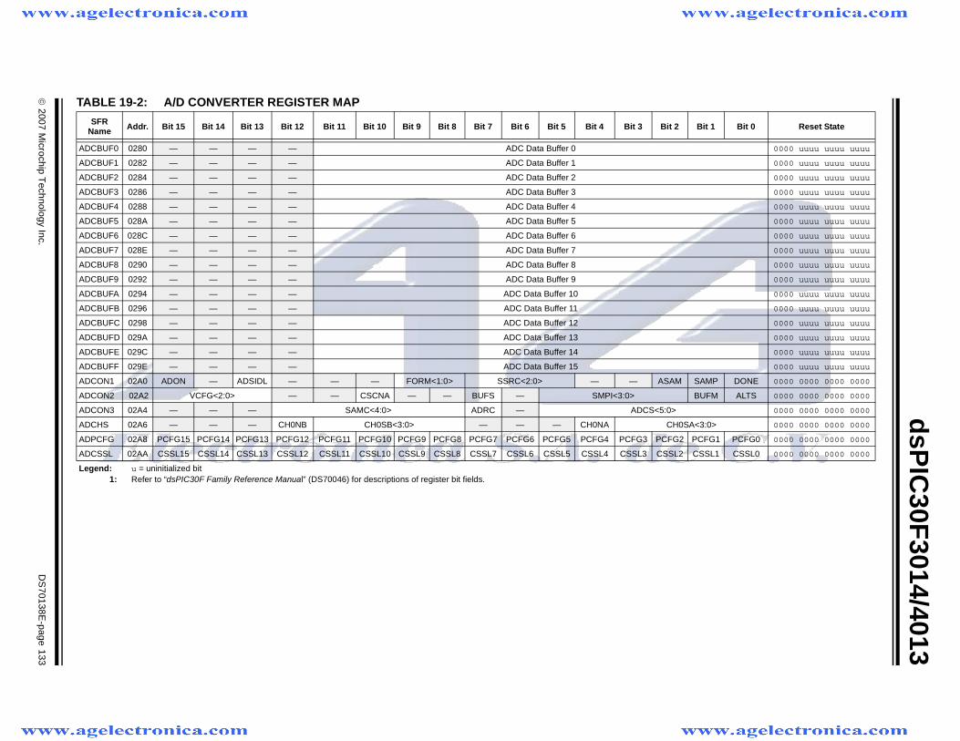
© 2007 M
icrochip Technology Inc.
DS
70138E-page 133
dsP
IC30F
3014/4013
TABLE 19-2: A/D CONVERTER REGISTER MAP
SFR Name Addr. Bit 15 Bit 14 Bit 13 Bit 12 Bit 11 Bit 10 Bit 9 Bit 8 Bit 7 Bit 6 Bit 5 Bit 4 Bit 3 Bit 2 Bit 1 Bit 0 Reset State
ADCBUF0 0280 — — — — ADC Data Buffer 0 0000 uuuu uuuu uuuu
ADCBUF1 0282 — — — — ADC Data Buffer 1 0000 uuuu uuuu uuuu
ADCBUF2 0284 — — — — ADC Data Buffer 2 0000 uuuu uuuu uuuu
ADCBUF3 0286 — — — — ADC Data Buffer 3 0000 uuuu uuuu uuuu
ADCBUF4 0288 — — — — ADC Data Buffer 4 0000 uuuu uuuu uuuu
ADCBUF5 028A — — — — ADC Data Buffer 5 0000 uuuu uuuu uuuu
ADCBUF6 028C — — — — ADC Data Buffer 6 0000 uuuu uuuu uuuu
ADCBUF7 028E — — — — ADC Data Buffer 7 0000 uuuu uuuu uuuu
ADCBUF8 0290 — — — — ADC Data Buffer 8 0000 uuuu uuuu uuuu
ADCBUF9 0292 — — — — ADC Data Buffer 9 0000 uuuu uuuu uuuu
ADCBUFA 0294 — — — — ADC Data Buffer 10 0000 uuuu uuuu uuuu
ADCBUFB 0296 — — — — ADC Data Buffer 11 0000 uuuu uuuu uuuu
ADCBUFC 0298 — — — — ADC Data Buffer 12 0000 uuuu uuuu uuuu
ADCBUFD 029A — — — — ADC Data Buffer 13 0000 uuuu uuuu uuuu
ADCBUFE 029C — — — — ADC Data Buffer 14 0000 uuuu uuuu uuuu
ADCBUFF 029E — — — — ADC Data Buffer 15 0000 uuuu uuuu uuuu
ADCON1 02A0 ADON — ADSIDL — — — FORM<1:0> SSRC<2:0> — — ASAM SAMP DONE 0000 0000 0000 0000
ADCON2 02A2 VCFG<2:0> — — CSCNA — — BUFS — SMPI<3:0> BUFM ALTS 0000 0000 0000 0000
ADCON3 02A4 — — — SAMC<4:0> ADRC — ADCS<5:0> 0000 0000 0000 0000
ADCHS 02A6 — — — CH0NB CH0SB<3:0> — — — CH0NA CH0SA<3:0> 0000 0000 0000 0000
ADPCFG 02A8 PCFG15 PCFG14 PCFG13 PCFG12 PCFG11 PCFG10 PCFG9 PCFG8 PCFG7 PCFG6 PCFG5 PCFG4 PCFG3 PCFG2 PCFG1 PCFG0 0000 0000 0000 0000
ADCSSL 02AA CSSL15 CSSL14 CSSL13 CSSL12 CSSL11 CSSL10 CSSL9 CSSL8 CSSL7 CSSL6 CSSL5 CSSL4 CSSL3 CSSL2 CSSL1 CSSL0 0000 0000 0000 0000
Legend: u = uninitialized bit1: Refer to “dsPIC30F Family Reference Manual” (DS70046) for descriptions of register bit fields.

dsPIC30F3014/4013
DS70138E-page 134 © 2007 Microchip Technology Inc.
NOTES:
© 2007 Microchip Technology Inc. DS70138E-page 135
dsPIC30F3014/4013
20.0 SYSTEM INTEGRATION
There are several features intended to maximizesystem reliability, minimize cost through elimination ofexternal components, provide power-saving operatingmodes and offer code protection:
• Oscillator Selection• Reset
- Power-on Reset (POR)
- Power-up Timer (PWRT)- Oscillator Start-up Timer (OST)- Programmable Brown-out Reset (BOR)
• Watchdog Timer (WDT)• Low-Voltage Detect• Power-Saving modes (Sleep and Idle)
• Code Protection• Unit ID Locations• In-Circuit Serial Programming (ICSP)
dsPIC30F devices have a Watchdog Timer which ispermanently enabled via the Configuration bits or canbe software controlled. It runs off its own RC oscillatorfor added reliability. There are two timers that offernecessary delays on power-up. One is the OscillatorStart-up Timer (OST), intended to keep the chip inReset until the crystal oscillator is stable. The other isthe Power-up Timer (PWRT) which provides a delay onpower-up only, designed to keep the part in Reset whilethe power supply stabilizes. With these two timers on-chip, most applications need no external Resetcircuitry.
Sleep mode is designed to offer a very low-currentPower-Down mode. The user can wake-up from Sleepthrough external Reset, Watchdog Timer Wake-up, orthrough an interrupt. Several oscillator options are alsomade available to allow the part to fit a wide variety ofapplications. In the Idle mode, the clock sources arestill active but the CPU is shut-off. The RC oscillatoroption saves system cost while the LP crystal optionsaves power.
20.1 Oscillator System Overview
The dsPIC30F oscillator system has the followingmodules and features:
• Various external and internal oscillator options as clock sources
• An on-chip PLL to boost internal operating frequency
• A clock switching mechanism between various clock sources
• Programmable clock postscaler for system power savings
• A Fail-Safe Clock Monitor (FSCM) that detects clock failure and takes fail-safe measures
• Clock Control register (OSCCON)• Configuration bits for main oscillator selection
Configuration bits determine the clock source uponPower-on Reset (POR) and Brown-out Reset (BOR).Thereafter, the clock source can be changed betweenpermissible clock sources. The OSCCON registercontrols the clock switching and reflects system clockrelated Status bits.
Table 20-1 provides a summary of the dsPIC30Foscillator operating modes. A simplified diagram of theoscillator system is shown in Figure 20-1.
Note: This data sheet summarizes features of this groupof dsPIC30F devices and is not intended to be a completereference source. For more information on the CPU,peripherals, register descriptions and general devicefunctionality, refer to the “dsPIC30F Family ReferenceManual” (DS70046). For more information on the deviceinstruction set and programming, refer to the “dsPIC30F/33F Programmer’s Reference Manual” (DS70157).
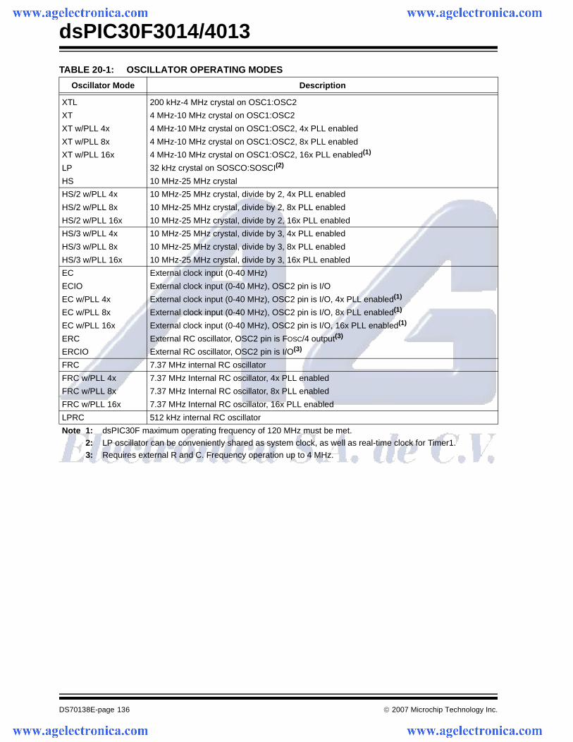
dsPIC30F3014/4013
DS70138E-page 136 © 2007 Microchip Technology Inc.
TABLE 20-1: OSCILLATOR OPERATING MODES
Oscillator Mode Description
XTL 200 kHz-4 MHz crystal on OSC1:OSC2
XT 4 MHz-10 MHz crystal on OSC1:OSC2
XT w/PLL 4x 4 MHz-10 MHz crystal on OSC1:OSC2, 4x PLL enabled
XT w/PLL 8x 4 MHz-10 MHz crystal on OSC1:OSC2, 8x PLL enabled
XT w/PLL 16x 4 MHz-10 MHz crystal on OSC1:OSC2, 16x PLL enabled(1)
LP 32 kHz crystal on SOSCO:SOSCI(2)
HS 10 MHz-25 MHz crystal
HS/2 w/PLL 4x 10 MHz-25 MHz crystal, divide by 2, 4x PLL enabled
HS/2 w/PLL 8x 10 MHz-25 MHz crystal, divide by 2, 8x PLL enabled
HS/2 w/PLL 16x 10 MHz-25 MHz crystal, divide by 2, 16x PLL enabled
HS/3 w/PLL 4x 10 MHz-25 MHz crystal, divide by 3, 4x PLL enabled
HS/3 w/PLL 8x 10 MHz-25 MHz crystal, divide by 3, 8x PLL enabled
HS/3 w/PLL 16x 10 MHz-25 MHz crystal, divide by 3, 16x PLL enabled
EC External clock input (0-40 MHz)
ECIO External clock input (0-40 MHz), OSC2 pin is I/O
EC w/PLL 4x External clock input (0-40 MHz), OSC2 pin is I/O, 4x PLL enabled(1)
EC w/PLL 8x External clock input (0-40 MHz), OSC2 pin is I/O, 8x PLL enabled(1)
EC w/PLL 16x External clock input (0-40 MHz), OSC2 pin is I/O, 16x PLL enabled(1)
ERC External RC oscillator, OSC2 pin is FOSC/4 output(3)
ERCIO External RC oscillator, OSC2 pin is I/O(3)
FRC 7.37 MHz internal RC oscillator
FRC w/PLL 4x 7.37 MHz Internal RC oscillator, 4x PLL enabled
FRC w/PLL 8x 7.37 MHz Internal RC oscillator, 8x PLL enabled
FRC w/PLL 16x 7.37 MHz Internal RC oscillator, 16x PLL enabled
LPRC 512 kHz internal RC oscillator
Note 1: dsPIC30F maximum operating frequency of 120 MHz must be met.
2: LP oscillator can be conveniently shared as system clock, as well as real-time clock for Timer1.3: Requires external R and C. Frequency operation up to 4 MHz.
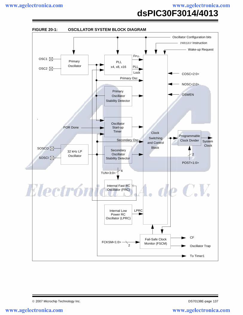
© 2007 Microchip Technology Inc. DS70138E-page 137
dsPIC30F3014/4013
FIGURE 20-1: OSCILLATOR SYSTEM BLOCK DIAGRAM
Primary OSC1
OSC2
SOSCO
SOSCI
Oscillator
32 kHz LP
Clock
and Control
Block
Switching
Oscillator
x4, x8, x16
PLL
Primary
Oscillator
Stability Detector
Stability Detector
SecondaryOscillator
ProgrammableClock Divider
OscillatorStart-upTimer
Fail-Safe ClockMonitor (FSCM)
Internal Fast RCOscillator (FRC)
Internal LowPower RC
Oscillator (LPRC)
PWRSAV Instruction
Wake-up Request
Oscillator Configuration bits
SystemClock
Oscillator Trap
To Timer1
LPRC
Secondary Osc
POR Done
Primary Osc
FPLL
POST<1:0>
2
FCKSM<1:0>2
PLL
Lock COSC<2:0>
NOSC<2:0>
OSWEN
CF
TUN<3:0>4
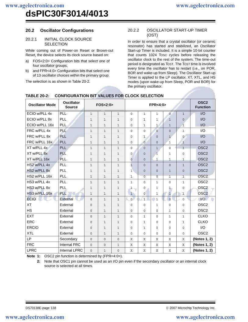
dsPIC30F3014/4013
DS70138E-page 138 © 2007 Microchip Technology Inc.
20.2 Oscillator Configurations
20.2.1 INITIAL CLOCK SOURCE SELECTION
While coming out of Power-on Reset or Brown-outReset, the device selects its clock source based on:
a) FOS<2:0> Configuration bits that select one offour oscillator groups,
b) and FPR<4:0> Configuration bits that select oneof 13 oscillator choices within the primary group.
The selection is as shown in Table 20-2.
20.2.2 OSCILLATOR START-UP TIMER (OST)
In order to ensure that a crystal oscillator (or ceramicresonator) has started and stabilized, an OscillatorStart-up Timer is included. It is a simple 10-bit counterthat counts 1024 TOSC cycles before releasing theoscillator clock to the rest of the system. The time-outperiod is designated as TOST. The TOST time is involvedevery time the oscillator has to restart (i.e., on POR,BOR and wake-up from Sleep). The Oscillator Start-upTimer is applied to the LP oscillator, XT, XTL, and HSmodes (upon wake-up from Sleep, POR and BOR) forthe primary oscillator.
TABLE 20-2: CONFIGURATION BIT VALUES FOR CLOCK SELECTION
Oscillator ModeOscillator
SourceFOS<2:0> FPR<4:0>
OSC2 Function
ECIO w/PLL 4x PLL 1 1 1 0 1 1 0 1 I/O
ECIO w/PLL 8x PLL 1 1 1 0 1 1 1 0 I/O
ECIO w/PLL 16x PLL 1 1 1 0 1 1 1 1 I/O
FRC w/PLL 4x PLL 1 1 1 0 0 0 0 1 I/O
FRC w/PLL 8x PLL 1 1 1 0 1 0 1 0 I/O
FRC w/PLL 16x PLL 1 1 1 0 0 0 1 1 I/O
XT w/PLL 4x PLL 1 1 1 0 0 1 0 1 OSC2
XT w/PLL 8x PLL 1 1 1 0 0 1 1 0 OSC2
XT w/PLL 16x PLL 1 1 1 0 0 1 1 1 OSC2
HS2 w/PLL 4x PLL 1 1 1 1 0 0 0 1 OSC2
HS2 w/PLL 8x PLL 1 1 1 1 0 0 1 0 OSC2
HS2 w/PLL 16x PLL 1 1 1 1 0 0 1 1 OSC2
HS3 w/PLL 4x PLL 1 1 1 1 0 1 0 1 OSC2
HS3 w/PLL 8x PLL 1 1 1 1 0 1 1 0 OSC2
HS3 w/PLL 16x PLL 1 1 1 1 0 1 1 1 OSC2
ECIO External 0 1 1 0 1 1 0 0 I/O
XT External 0 1 1 0 0 1 0 0 OSC2
HS External 0 1 1 0 0 0 1 0 OSC2
EXT External 0 1 1 0 1 0 1 1 CLKO
ERC External 0 1 1 0 1 0 0 1 CLKO
ERCIO External 0 1 1 0 1 0 0 0 I/O
XTL External 0 1 1 0 0 0 0 0 OSC2
LP Secondary 0 0 0 X X X X X (Notes 1, 2)
FRC Internal FRC 0 0 1 X X X X X (Notes 1, 2)
LPRC Internal LPRC 0 1 0 X X X X X (Notes 1, 2)
Note 1: OSC2 pin function is determined by (FPR<4:0>).2: Note that OSC1 pin cannot be used as an I/O pin even if the secondary oscillator or an internal clock
source is selected at all times.
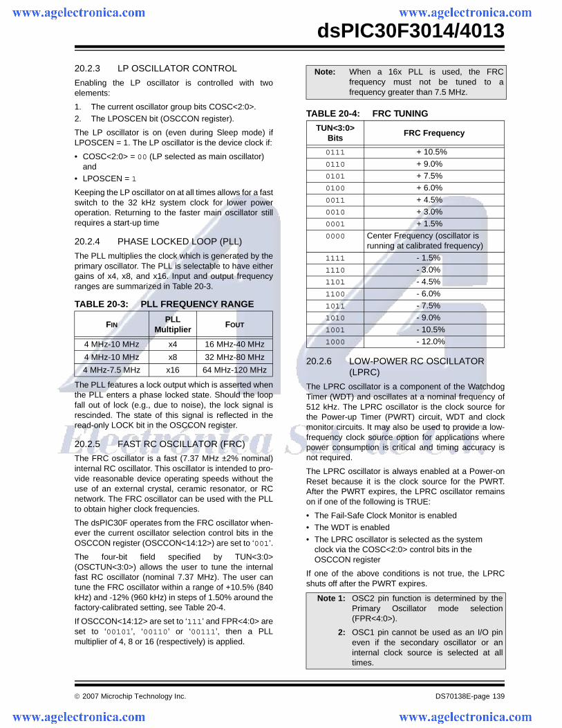
© 2007 Microchip Technology Inc. DS70138E-page 139
dsPIC30F3014/4013
20.2.3 LP OSCILLATOR CONTROL
Enabling the LP oscillator is controlled with twoelements:
1. The current oscillator group bits COSC<2:0>.2. The LPOSCEN bit (OSCCON register).
The LP oscillator is on (even during Sleep mode) ifLPOSCEN = 1. The LP oscillator is the device clock if:
• COSC<2:0> = 00 (LP selected as main oscillator)and
• LPOSCEN = 1
Keeping the LP oscillator on at all times allows for a fastswitch to the 32 kHz system clock for lower poweroperation. Returning to the faster main oscillator stillrequires a start-up time
20.2.4 PHASE LOCKED LOOP (PLL)
The PLL multiplies the clock which is generated by theprimary oscillator. The PLL is selectable to have eithergains of x4, x8, and x16. Input and output frequencyranges are summarized in Table 20-3.
TABLE 20-3: PLL FREQUENCY RANGE
The PLL features a lock output which is asserted whenthe PLL enters a phase locked state. Should the loopfall out of lock (e.g., due to noise), the lock signal isrescinded. The state of this signal is reflected in theread-only LOCK bit in the OSCCON register.
20.2.5 FAST RC OSCILLATOR (FRC)
The FRC oscillator is a fast (7.37 MHz ±2% nominal)internal RC oscillator. This oscillator is intended to pro-vide reasonable device operating speeds without theuse of an external crystal, ceramic resonator, or RCnetwork. The FRC oscillator can be used with the PLLto obtain higher clock frequencies.
The dsPIC30F operates from the FRC oscillator when-ever the current oscillator selection control bits in theOSCCON register (OSCCON<14:12>) are set to ‘001’.
The four-bit field specified by TUN<3:0>(OSCTUN<3:0>) allows the user to tune the internalfast RC oscillator (nominal 7.37 MHz). The user cantune the FRC oscillator within a range of +10.5% (840kHz) and -12% (960 kHz) in steps of 1.50% around thefactory-calibrated setting, see Table 20-4.
If OSCCON<14:12> are set to ‘111’ and FPR<4:0> areset to ‘00101’, ‘00110’ or ‘00111’, then a PLLmultiplier of 4, 8 or 16 (respectively) is applied.
TABLE 20-4: FRC TUNING
20.2.6 LOW-POWER RC OSCILLATOR (LPRC)
The LPRC oscillator is a component of the WatchdogTimer (WDT) and oscillates at a nominal frequency of512 kHz. The LPRC oscillator is the clock source forthe Power-up Timer (PWRT) circuit, WDT and clockmonitor circuits. It may also be used to provide a low-frequency clock source option for applications wherepower consumption is critical and timing accuracy isnot required.
The LPRC oscillator is always enabled at a Power-onReset because it is the clock source for the PWRT.After the PWRT expires, the LPRC oscillator remainson if one of the following is TRUE:
• The Fail-Safe Clock Monitor is enabled• The WDT is enabled
• The LPRC oscillator is selected as the system clock via the COSC<2:0> control bits in the OSCCON register
If one of the above conditions is not true, the LPRCshuts off after the PWRT expires.
FINPLL
MultiplierFOUT
4 MHz-10 MHz x4 16 MHz-40 MHz
4 MHz-10 MHz x8 32 MHz-80 MHz
4 MHz-7.5 MHz x16 64 MHz-120 MHz
Note: When a 16x PLL is used, the FRCfrequency must not be tuned to afrequency greater than 7.5 MHz.
TUN<3:0>Bits
FRC Frequency
0111 + 10.5%
0110 + 9.0%0101 + 7.5%0100 + 6.0%
0011 + 4.5%0010 + 3.0%0001 + 1.5%
0000 Center Frequency (oscillator isrunning at calibrated frequency)
1111 - 1.5%1110 - 3.0%1101 - 4.5%
1100 - 6.0%1011 - 7.5%1010 - 9.0%
1001 - 10.5%1000 - 12.0%
Note 1: OSC2 pin function is determined by thePrimary Oscillator mode selection(FPR<4:0>).
2: OSC1 pin cannot be used as an I/O pineven if the secondary oscillator or aninternal clock source is selected at alltimes.
dsPIC30F3014/4013
DS70138E-page 140 © 2007 Microchip Technology Inc.
20.2.7 FAIL-SAFE CLOCK MONITOR
The Fail-Safe Clock Monitor (FSCM) allows the deviceto continue to operate even in the event of an oscillatorfailure. The FSCM function is enabled by appropriatelyprogramming the FCKSM Configuration bits (clockswitch and monitor selection bits) in the FOSC DeviceConfiguration register. If the FSCM function is enabled,the LPRC internal oscillator runs at all times (exceptduring Sleep mode) and is not subject to control by theSWDTEN bit.
In the event of an oscillator failure, the FSCMgenerates a clock failure trap event and switches thesystem clock over to the FRC oscillator. The user thenhas the option to either attempt to restart the oscillatoror execute a controlled shutdown. The user may decideto treat the trap as a warm Reset by simply loading theReset address into the oscillator fail trap vector. In thisevent, the CF (Clock Fail) Status bit (OSCCON<3>) isalso set whenever a clock failure is recognized.
In the event of a clock failure, the WDT is unaffectedand continues to run on the LPRC clock.
If the oscillator has a very slow start-up time coming outof POR, BOR or Sleep, it is possible that the PWRTtimer will expire before the oscillator has started. Insuch cases, the FSCM is activated and the FSCM ini-tiates a clock failure trap, and the COSC<2:0> bits areloaded with FRC oscillator selection. This effectivelyshuts off the original oscillator that was trying to start.
The user may detect this situation and restart theoscillator in the clock fail trap ISR.
Upon a clock failure detection, the FSCM moduleinitiates a clock switch to the FRC oscillator as follows:
1. The COSC bits (OSCCON<14:12>) are loadedwith the FRC oscillator selection value.
2. CF bit is set (OSCCON<3>).3. OSWEN control bit (OSCCON<0>) is cleared.
For the purpose of clock switching, the clock sourcesare sectioned into four groups:
1. Primary2. Secondary
3. Internal FRC4. Internal LPRC
The user can switch between these functional groupsbut cannot switch between options within a group. If theprimary group is selected, then the choice within thegroup is always determined by the FPR<4:0> Configu-ration bits.
The OSCCON register holds the control and Status bitsrelated to clock switching.
• COSC<2:0>: Read-only Status bits always reflect the current oscillator group in effect.
• NOSC<2:0>: Control bits which are written to indicate the new oscillator group of choice.
- On POR and BOR, COSC<2:0> and NOSC<2:0> are both loaded with the Config-uration bit values FOS<2:0>.
• LOCK: The LOCK Status bit indicates a PLL lock.
• CF: Read-only Status bit indicating if a clock fail detect has occurred.
• OSWEN: Control bit changes from a ‘0’ to a ‘1’ when a clock transition sequence is initiated. Clearing the OSWEN control bit aborts a clock transition in progress (used for hang-up situations).
If Configuration bits FCKSM<1:0> = 1x, then the clockswitching and Fail-Safe Clock monitoring functions aredisabled. This is the default Configuration bit setting.
If clock switching is disabled, then the FOS<2:0> andFPR<4:0> bits directly control the oscillator selectionand the COSC<2:0> bits do not control the clockselection. However, these bits reflect the clock sourceselection.
20.2.8 PROTECTION AGAINST ACCIDENTAL WRITES TO OSCCON
A write to the OSCCON register is intentionally madedifficult because it controls clock switching and clockscaling.
To write to the OSCCON low byte, the following codesequence must be executed without any otherinstructions in between:
Byte write is allowed for one instruction cycle. Write thedesired value or use bit manipulation instruction.
To write to the OSCCON high byte, the followinginstructions must be executed without any otherinstructions in between:
Byte write is allowed for one instruction cycle. Write thedesired value or use bit manipulation instruction.
Note: The application should not attempt toswitch to a clock of frequency lower than100 KHz when the Fail-Safe Clock Monitoris enabled. If such clock switching isperformed, the device may generate anoscillator fail trap and switch to the Fast RCoscillator.
Byte Write “0x46” to OSCCON lowByte Write “0x57” to OSCCON low
Byte Write “0x78” to OSCCON highByte Write “0x9A” to OSCCON high
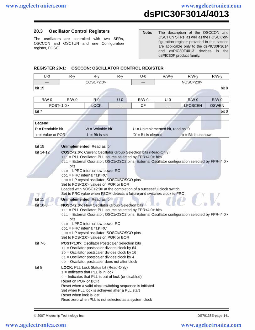
© 2007 Microchip Technology Inc. DS70138E-page 141
dsPIC30F3014/4013
20.3 Oscillator Control Registers
The oscillators are controlled with two SFRs,OSCCON and OSCTUN and one Configurationregister, FOSC.
Note: The description of the OSCCON andOSCTUN SFRs, as well as the FOSC Con-figuration register provided in this sectionare applicable only to the dsPIC30F3014and dsPIC30F4013 devices in thedsPIC30F product family.
REGISTER 20-1: OSCCON: OSCILLATOR CONTROL REGISTER
U-0 R-y R-y R-y U-0 R/W-y R/W-y R/W-y
— COSC<2:0> — NOSC<2:0>
bit 15 bit 8
R/W-0 R/W-0 R-0 U-0 R/W-0 U-0 R/W-0 R/W-0
POST<1:0> LOCK — CF — LPOSCEN OSWEN
bit 7 bit 0
Legend:
R = Readable bit W = Writable bit U = Unimplemented bit, read as ‘0’
-n = Value at POR ‘1’ = Bit is set ‘0’ = Bit is cleared x = Bit is unknown
bit 15 Unimplemented: Read as ‘0’
bit 14-12 COSC<2:0>: Current Oscillator Group Selection bits (Read-Only)111 = PLL Oscillator; PLL source selected by FPR<4:0> bits011 = External Oscillator; OSC1/OSC2 pins; External Oscillator configuration selected by FPR<4:0>
bits010 = LPRC internal low-power RC001 = FRC internal fast RC000 = LP crystal oscillator; SOSCI/SOSCO pinsSet to FOS<2:0> values on POR or BORLoaded with NOSC<2:0> at the completion of a successful clock switchSet to FRC value when FSCM detects a failure and switches clock to FRC
bit 11 Unimplemented: Read as ‘0’
bit 10-8 NOSC<2:0>: New Oscillator Group Selection bits111 = PLL Oscillator; PLL source selected by FPR<4:0> bits011 = External Oscillator; OSC1/OSC2 pins; External Oscillator configuration selected by FPR<4:0>
bits010 = LPRC internal low-power RC001 = FRC internal fast RC000 = LP crystal oscillator; SOSCI/SOSCO pinsSet to FOS<2:0> values on POR or BOR
bit 7-6 POST<1:0>: Oscillator Postscaler Selection bits11 = Oscillator postscaler divides clock by 6410 = Oscillator postscaler divides clock by 1601 = Oscillator postscaler divides clock by 400 = Oscillator postscaler does not alter clock
bit 5 LOCK: PLL Lock Status bit (Read-Only)1 = Indicates that PLL is in lock0 = Indicates that PLL is out of lock (or disabled)Reset on POR or BORReset when a valid clock switching sequence is initiatedSet when PLL lock is achieved after a PLL startReset when lock is lostRead zero when PLL is not selected as a system clock
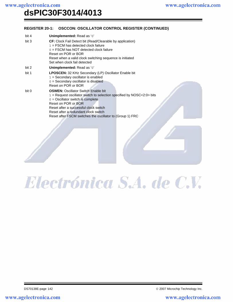
dsPIC30F3014/4013
DS70138E-page 142 © 2007 Microchip Technology Inc.
bit 4 Unimplemented: Read as ‘0’
bit 3 CF: Clock Fail Detect bit (Read/Clearable by application)1 = FSCM has detected clock failure0 = FSCM has NOT detected clock failureReset on POR or BORReset when a valid clock switching sequence is initiatedSet when clock fail detected
bit 2 Unimplemented: Read as ‘0’
bit 1 LPOSCEN: 32 KHz Secondary (LP) Oscillator Enable bit1 = Secondary oscillator is enabled0 = Secondary oscillator is disabledReset on POR or BOR
bit 0 OSWEN: Oscillator Switch Enable bit1 = Request oscillator switch to selection specified by NOSC<2:0> bits0 = Oscillator switch is completeReset on POR or BORReset after a successful clock switchReset after a redundant clock switchReset after FSCM switches the oscillator to (Group 1) FRC
REGISTER 20-1: OSCCON: OSCILLATOR CONTROL REGISTER (CONTINUED)
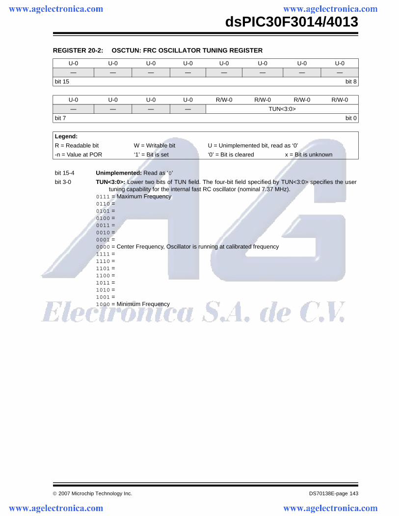
© 2007 Microchip Technology Inc. DS70138E-page 143
dsPIC30F3014/4013
REGISTER 20-2: OSCTUN: FRC OSCILLATOR TUNING REGISTER
U-0 U-0 U-0 U-0 U-0 U-0 U-0 U-0
— — — — — — — —
bit 15 bit 8
U-0 U-0 U-0 U-0 R/W-0 R/W-0 R/W-0 R/W-0
— — — — TUN<3:0>
bit 7 bit 0
Legend:
R = Readable bit W = Writable bit U = Unimplemented bit, read as ‘0’
-n = Value at POR ‘1’ = Bit is set ‘0’ = Bit is cleared x = Bit is unknown
bit 15-4 Unimplemented: Read as ‘0’
bit 3-0 TUN<3:0>: Lower two bits of TUN field. The four-bit field specified by TUN<3:0> specifies the usertuning capability for the internal fast RC oscillator (nominal 7.37 MHz).
0111 = Maximum Frequency0110 = 0101 = 0100 = 0011 = 0010 = 0001 = 0000 = Center Frequency, Oscillator is running at calibrated frequency1111 = 1110 = 1101 = 1100 = 1011 = 1010 = 1001 = 1000 = Minimum Frequency
dsPIC30F3014/4013
DS70138E-page 144 © 2007 Microchip Technology Inc.
REGISTER 20-3: FOSC: OSCILLATOR CONFIGURATION REGISTER
U U U U U U U U
— — — — — — — —
bit 23 bit 16
R/P R/P U U U R/P R/P R/P
FCKSM<1:0> — — — FOS<2:0>
bit 15 bit 8
U U U R/P R/P R/P R/P R/P
— — — FPR<4:0>
bit 7 bit 0
Legend:
R = Readable bit W = Writable bit U = Unimplemented bit, read as ‘0’
-n = Value at POR ‘1’ = Bit is set ‘0’ = Bit is cleared x = Bit is unknown
bit 23-16 Unimplemented: Read as ‘0’
bit 15-14 FCKSM<1:0>: Clock Switching and Monitor Selection Configuration bits1x = Clock switching is disabled, Fail-Safe Clock Monitor is disabled01 = Clock switching is enabled, Fail-Safe Clock Monitor is disabled00 = Clock switching is enabled, Fail-Safe Clock Monitor is enabled
bit 13-11 Unimplemented: Read as ‘0’
bit 10-8 FOS<2:0>: Oscillator Group Selection on POR bits111 = PLL Oscillator; PLL source selected by FPR<4:0> bits. See Table 20-2.011 = EXT: External Oscillator; OSC1/OSC2 pins; External Oscillator configuration selected by
FPR<4:0> bits010 = LPRC: Internal Low-Power RC001 = FRC: Internal Fast RC000 = LPOSC: Low-Power Crystal Oscillator; SOSCI/SOSCO pins
bit 7-4 Unimplemented: Read as ‘0’
bit 3-0 FPR<4:0>: Oscillator Selection within Primary Group bits. See Table 20-2.
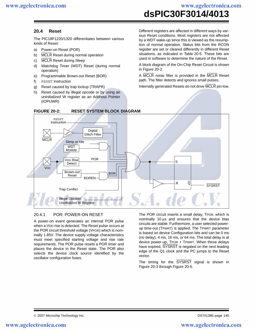
© 2007 Microchip Technology Inc. DS70138E-page 145
dsPIC30F3014/4013
20.4 Reset
The PIC18F1220/1320 differentiates between variouskinds of Reset:
a) Power-on Reset (POR) b) MCLR Reset during normal operation
c) MCLR Reset during Sleep d) Watchdog Timer (WDT) Reset (during normal
operation)e) Programmable Brown-out Reset (BOR) f) RESET Instruction
g) Reset caused by trap lockup (TRAPR)h) Reset caused by illegal opcode or by using an
uninitialized W register as an Address Pointer(IOPUWR)
Different registers are affected in different ways by var-ious Reset conditions. Most registers are not affectedby a WDT wake-up since this is viewed as the resump-tion of normal operation. Status bits from the RCONregister are set or cleared differently in different Resetsituations, as indicated in Table 20-5. These bits areused in software to determine the nature of the Reset.
A block diagram of the On-Chip Reset Circuit is shownin Figure 20-2.
A MCLR noise filter is provided in the MCLR Resetpath. The filter detects and ignores small pulses.
Internally generated Resets do not drive MCLR pin low.
FIGURE 20-2: RESET SYSTEM BLOCK DIAGRAM
20.4.1 POR: POWER-ON RESET
A power-on event generates an internal POR pulsewhen a VDD rise is detected. The Reset pulse occurs atthe POR circuit threshold voltage (VPOR) which is nom-inally 1.85V. The device supply voltage characteristicsmust meet specified starting voltage and rise raterequirements. The POR pulse resets a POR timer andplaces the device in the Reset state. The POR alsoselects the device clock source identified by theoscillator configuration fuses.
The POR circuit inserts a small delay, TPOR, which isnominally 10 μs and ensures that the device biascircuits are stable. Furthermore, a user selected power-up time-out (TPWRT) is applied. The TPWRT parameteris based on device Configuration bits and can be 0 ms(no delay), 4 ms, 16 ms, or 64 ms. The total delay is atdevice power-up, TPOR + TPWRT. When these delayshave expired, SYSRST is negated on the next leadingedge of the Q1 clock and the PC jumps to the Resetvector.
The timing for the SYSRST signal is shown inFigure 20-3 through Figure 20-5.
S
R Q
MCLR
VDD
VDD RiseDetect
POR
SYSRST
Sleep or Idle
Brown-outReset
BOREN
RESETInstruction
WDTModule
DigitalGlitch Filter
BOR
Trap Conflict
Illegal Opcode/Uninitialized W Register
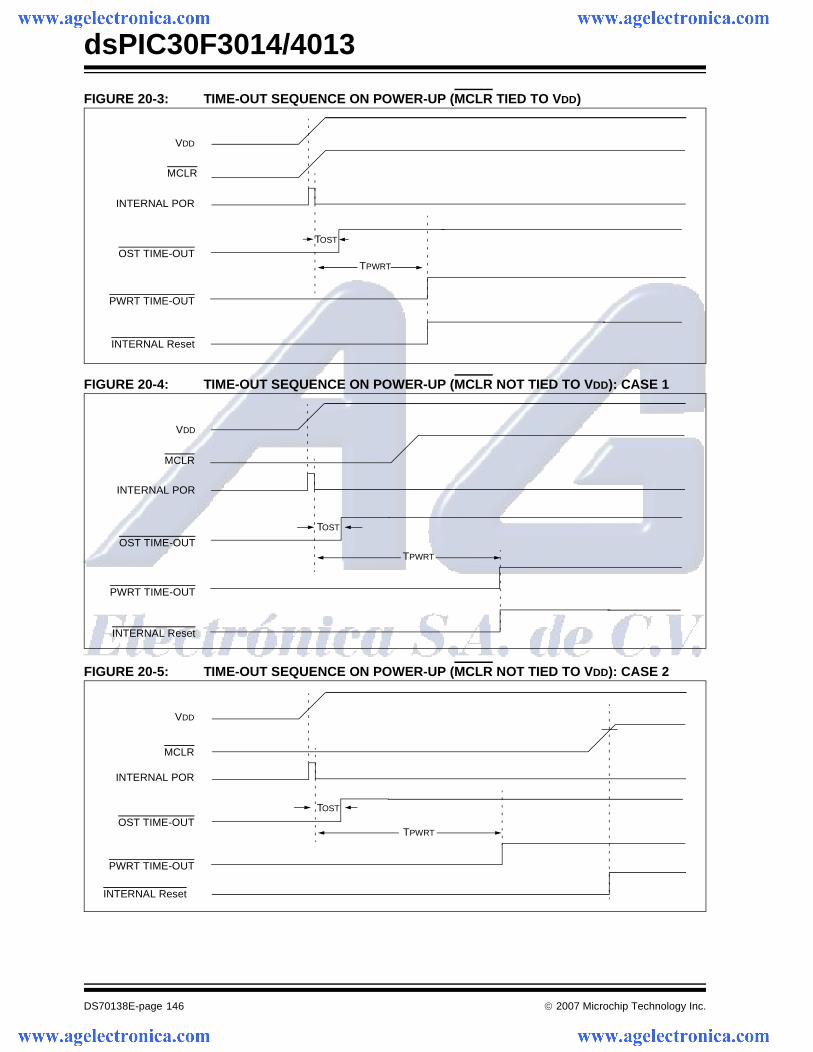
dsPIC30F3014/4013
DS70138E-page 146 © 2007 Microchip Technology Inc.
FIGURE 20-3: TIME-OUT SEQUENCE ON POWER-UP (MCLR TIED TO VDD)
FIGURE 20-4: TIME-OUT SEQUENCE ON POWER-UP (MCLR NOT TIED TO VDD): CASE 1
FIGURE 20-5: TIME-OUT SEQUENCE ON POWER-UP (MCLR NOT TIED TO VDD): CASE 2
TPWRT
TOST
VDD
INTERNAL POR
PWRT TIME-OUT
OST TIME-OUT
INTERNAL Reset
MCLR
TPWRT
TOST
VDD
INTERNAL POR
PWRT TIME-OUT
OST TIME-OUT
INTERNAL Reset
MCLR
VDD
MCLR
INTERNAL POR
PWRT TIME-OUT
OST TIME-OUT
INTERNAL Reset
TPWRT
TOST
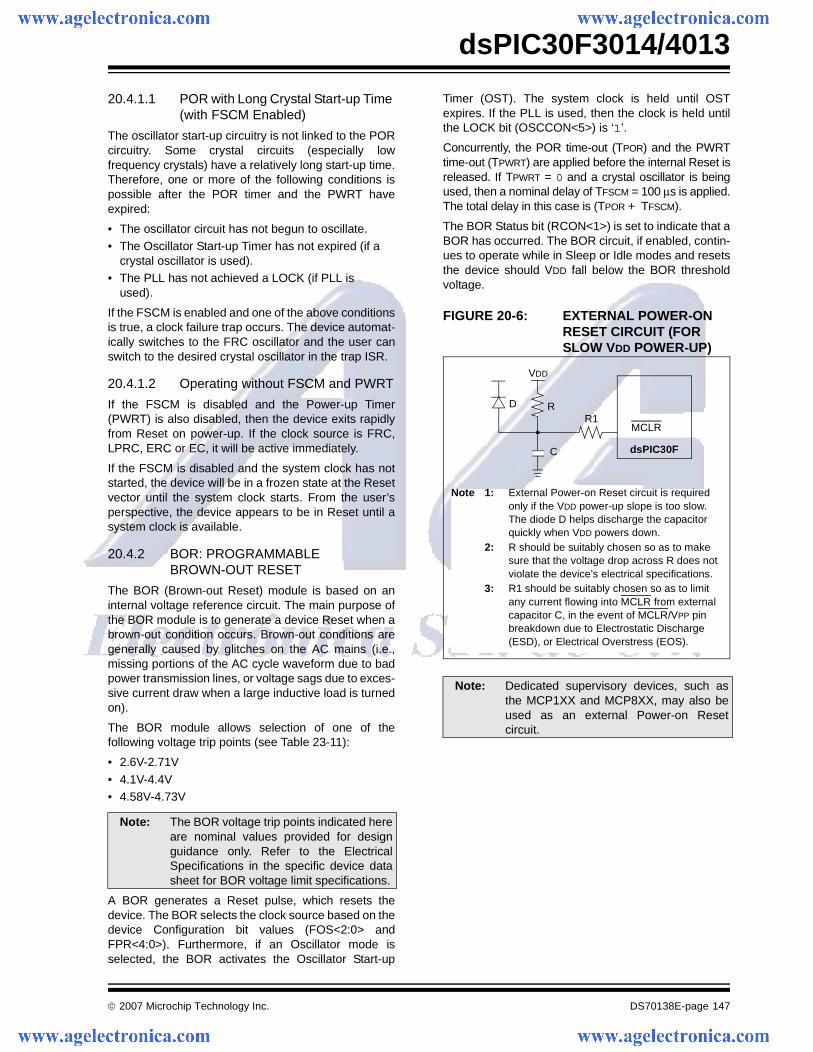
© 2007 Microchip Technology Inc. DS70138E-page 147
dsPIC30F3014/4013
20.4.1.1 POR with Long Crystal Start-up Time (with FSCM Enabled)
The oscillator start-up circuitry is not linked to the PORcircuitry. Some crystal circuits (especially lowfrequency crystals) have a relatively long start-up time.Therefore, one or more of the following conditions ispossible after the POR timer and the PWRT haveexpired:
• The oscillator circuit has not begun to oscillate.• The Oscillator Start-up Timer has not expired (if a
crystal oscillator is used).• The PLL has not achieved a LOCK (if PLL is
used).
If the FSCM is enabled and one of the above conditionsis true, a clock failure trap occurs. The device automat-ically switches to the FRC oscillator and the user canswitch to the desired crystal oscillator in the trap ISR.
20.4.1.2 Operating without FSCM and PWRT
If the FSCM is disabled and the Power-up Timer(PWRT) is also disabled, then the device exits rapidlyfrom Reset on power-up. If the clock source is FRC,LPRC, ERC or EC, it will be active immediately.
If the FSCM is disabled and the system clock has notstarted, the device will be in a frozen state at the Resetvector until the system clock starts. From the user’sperspective, the device appears to be in Reset until asystem clock is available.
20.4.2 BOR: PROGRAMMABLE BROWN-OUT RESET
The BOR (Brown-out Reset) module is based on aninternal voltage reference circuit. The main purpose ofthe BOR module is to generate a device Reset when abrown-out condition occurs. Brown-out conditions aregenerally caused by glitches on the AC mains (i.e.,missing portions of the AC cycle waveform due to badpower transmission lines, or voltage sags due to exces-sive current draw when a large inductive load is turnedon).
The BOR module allows selection of one of thefollowing voltage trip points (see Table 23-11):
• 2.6V-2.71V
• 4.1V-4.4V• 4.58V-4.73V
A BOR generates a Reset pulse, which resets thedevice. The BOR selects the clock source based on thedevice Configuration bit values (FOS<2:0> andFPR<4:0>). Furthermore, if an Oscillator mode isselected, the BOR activates the Oscillator Start-up
Timer (OST). The system clock is held until OSTexpires. If the PLL is used, then the clock is held untilthe LOCK bit (OSCCON<5>) is ‘1’.
Concurrently, the POR time-out (TPOR) and the PWRTtime-out (TPWRT) are applied before the internal Reset isreleased. If TPWRT = 0 and a crystal oscillator is beingused, then a nominal delay of TFSCM = 100 μs is applied.The total delay in this case is (TPOR + TFSCM).
The BOR Status bit (RCON<1>) is set to indicate that aBOR has occurred. The BOR circuit, if enabled, contin-ues to operate while in Sleep or Idle modes and resetsthe device should VDD fall below the BOR thresholdvoltage.
FIGURE 20-6: EXTERNAL POWER-ON RESET CIRCUIT (FOR SLOW VDD POWER-UP)
Note: The BOR voltage trip points indicated hereare nominal values provided for designguidance only. Refer to the ElectricalSpecifications in the specific device datasheet for BOR voltage limit specifications.
Note: Dedicated supervisory devices, such asthe MCP1XX and MCP8XX, may also beused as an external Power-on Resetcircuit.
Note 1: External Power-on Reset circuit is required only if the VDD power-up slope is too slow. The diode D helps discharge the capacitor quickly when VDD powers down.
2: R should be suitably chosen so as to make sure that the voltage drop across R does not violate the device’s electrical specifications.
3: R1 should be suitably chosen so as to limit any current flowing into MCLR from external capacitor C, in the event of MCLR/VPP pin breakdown due to Electrostatic Discharge (ESD), or Electrical Overstress (EOS).
C
R1RD
VDD
dsPIC30F
MCLR
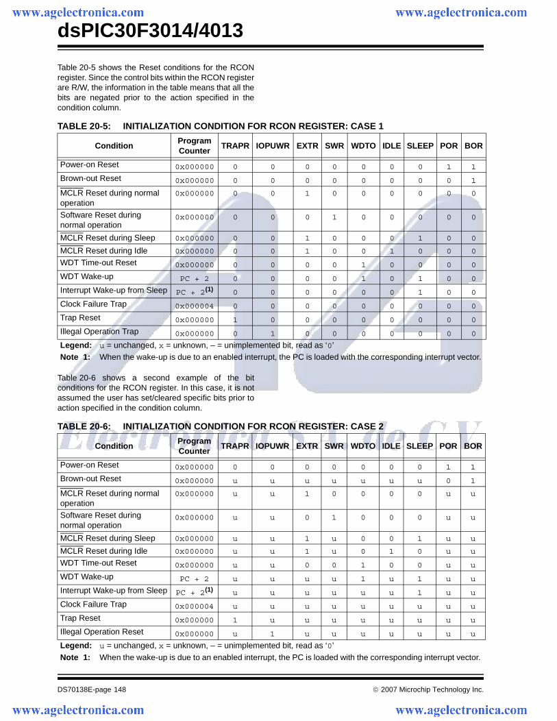
dsPIC30F3014/4013
DS70138E-page 148 © 2007 Microchip Technology Inc.
Table 20-5 shows the Reset conditions for the RCONregister. Since the control bits within the RCON registerare R/W, the information in the table means that all thebits are negated prior to the action specified in thecondition column.
TABLE 20-5: INITIALIZATION CONDITION FOR RCON REGISTER: CASE 1
Table 20-6 shows a second example of the bitconditions for the RCON register. In this case, it is notassumed the user has set/cleared specific bits prior toaction specified in the condition column.
TABLE 20-6: INITIALIZATION CONDITION FOR RCON REGISTER: CASE 2
ConditionProgramCounter
TRAPR IOPUWR EXTR SWR WDTO IDLE SLEEP POR BOR
Power-on Reset 0x000000 0 0 0 0 0 0 0 1 1
Brown-out Reset 0x000000 0 0 0 0 0 0 0 0 1
MCLR Reset during normaloperation
0x000000 0 0 1 0 0 0 0 0 0
Software Reset during normal operation
0x000000 0 0 0 1 0 0 0 0 0
MCLR Reset during Sleep 0x000000 0 0 1 0 0 0 1 0 0
MCLR Reset during Idle 0x000000 0 0 1 0 0 1 0 0 0
WDT Time-out Reset 0x000000 0 0 0 0 1 0 0 0 0
WDT Wake-up PC + 2 0 0 0 0 1 0 1 0 0
Interrupt Wake-up from Sleep PC + 2(1) 0 0 0 0 0 0 1 0 0
Clock Failure Trap 0x000004 0 0 0 0 0 0 0 0 0
Trap Reset 0x000000 1 0 0 0 0 0 0 0 0
Illegal Operation Trap 0x000000 0 1 0 0 0 0 0 0 0
Legend: u = unchanged, x = unknown, – = unimplemented bit, read as ‘0’Note 1: When the wake-up is due to an enabled interrupt, the PC is loaded with the corresponding interrupt vector.
ConditionProgramCounter
TRAPR IOPUWR EXTR SWR WDTO IDLE SLEEP POR BOR
Power-on Reset 0x000000 0 0 0 0 0 0 0 1 1
Brown-out Reset 0x000000 u u u u u u u 0 1
MCLR Reset during normal operation
0x000000 u u 1 0 0 0 0 u u
Software Reset during normal operation
0x000000 u u 0 1 0 0 0 u u
MCLR Reset during Sleep 0x000000 u u 1 u 0 0 1 u u
MCLR Reset during Idle 0x000000 u u 1 u 0 1 0 u u
WDT Time-out Reset 0x000000 u u 0 0 1 0 0 u u
WDT Wake-up PC + 2 u u u u 1 u 1 u u
Interrupt Wake-up from Sleep PC + 2(1) u u u u u u 1 u u
Clock Failure Trap 0x000004 u u u u u u u u u
Trap Reset 0x000000 1 u u u u u u u u
Illegal Operation Reset 0x000000 u 1 u u u u u u u
Legend: u = unchanged, x = unknown, – = unimplemented bit, read as ‘0’
Note 1: When the wake-up is due to an enabled interrupt, the PC is loaded with the corresponding interrupt vector.
© 2007 Microchip Technology Inc. DS70138E-page 149
dsPIC30F3014/4013
20.5 Watchdog Timer (WDT)
20.5.1 WATCHDOG TIMER OPERATION
The primary function of the Watchdog Timer (WDT) isto reset the processor in the event of a software mal-function. The WDT is a free-running timer that runs offan on-chip RC oscillator, requiring no external compo-nent. Therefore, the WDT timer continues to operateeven if the main processor clock (e.g., the crystaloscillator) fails.
20.5.2 ENABLING AND DISABLING THE WDT
The Watchdog Timer can be “Enabled” or “Disabled”only through a Configuration bit (FWDTEN) in theConfiguration register, FWDT.
Setting FWDTEN = 1 enables the Watchdog Timer. Theenabling is done when programming the device. Bydefault, after chip erase, FWDTEN bit = 1. Any deviceprogrammer capable of programming dsPIC30Fdevices allows programming of this and otherConfiguration bits.
If enabled, the WDT increments until it overflows or“times out”. A WDT time-out forces a device Reset(except during Sleep). To prevent a WDT time-out, theuser must clear the Watchdog Timer using a CLRWDTinstruction.
If a WDT times out during Sleep, the device wakes up.The WDTO bit in the RCON register is cleared to indi-cate a wake-up resulting from a WDT time-out.
Setting FWDTEN = 0 allows user software to enable/disable the Watchdog Timer via the SWDTEN(RCON<5>) control bit.
20.6 Low-Voltage Detect
The Low-Voltage Detect (LVD) module is used todetect when the VDD of the device drops below athreshold value, VLVD, which is determined by theLVDL<3:0> bits (RCON<11:8>) and is thus user pro-grammable. The internal voltage reference circuitryrequires a nominal amount of time to stabilize, and theBGST bit (RCON<13>) indicates when the voltage ref-erence has stabilized.
In some devices, the LVD threshold voltage may beapplied externally on the LVDIN pin.
The LVD module is enabled by setting the LVDEN bit(RCON<12>).
20.7 Power-Saving Modes
There are two power-saving states that can be enteredthrough the execution of a special instruction, PWRSAV;these are Sleep and Idle.
The format of the PWRSAV instruction is as follows:
PWRSAV <parameter>, where ‘parameter’ definesIdle or Sleep mode.
20.7.1 SLEEP MODE
In Sleep mode, the clock to the CPU and peripherals isshut down. If an on-chip oscillator is being used, it isshut down.
The Fail-Safe Clock Monitor is not functional duringSleep since there is no clock to monitor. However,LPRC clock remains active if WDT is operational duringSleep.
The brown-out protection circuit and the Low-VoltageDetect circuit, if enabled, remains functional duringSleep.
The processor wakes up from Sleep if at least one ofthe following conditions has occurred:
• any interrupt that is individually enabled and meets the required priority level
• any Reset (POR, BOR and MCLR) • WDT time-out
On waking up from Sleep mode, the processor restartsthe same clock that was active prior to entry into Sleepmode. When clock switching is enabled, bitsCOSC<2:0> determine the oscillator source to be usedon wake-up. If clock switch is disabled, then there isonly one system clock.
If the clock source is an oscillator, the clock to thedevice is held off until OST times out (indicating a sta-ble oscillator). If PLL is used, the system clock is heldoff until LOCK = 1 (indicating that the PLL is stable). Ineither case, TPOR, TLOCK and TPWRT delays areapplied.
If EC, FRC, LPRC or ERC oscillators are used, then adelay of TPOR (~ 10 μs) is applied. This is the smallestdelay possible on wake-up from Sleep.
Moreover, if LP oscillator was active during Sleep andLP is the oscillator used on wake-up, then the start-updelay is equal to TPOR. PWRT delay and OST timerdelay are not applied. In order to have the smallestpossible start-up delay when waking up from Sleep,one of these faster wake-up options should be selectedbefore entering Sleep.
Note: If a POR or BOR occurred, the selection ofthe oscillator is based on the FOS<2:0>and FPR<4:0> Configuration bits.
dsPIC30F3014/4013
DS70138E-page 150 © 2007 Microchip Technology Inc.
Any interrupt that is individually enabled (using the cor-responding IE bit) and meets the prevailing priority levelcan wake-up the processor. The processor processesthe interrupt and branch to the ISR. The Sleep Status bitin the RCON register is set upon wake-up.
All Resets wake up the processor from Sleep mode.Any Reset, other than POR, sets the Sleep Status bit.In a POR, the Sleep bit is cleared.
If the Watchdog Timer is enabled, the processor wakesup from Sleep mode upon WDT time-out. The Sleepand WDTO Status bits are both set.
20.7.2 IDLE MODE
In Idle mode, the clock to the CPU is shut down whileperipherals keep running. Unlike Sleep mode, the clocksource remains active.
Several peripherals have a control bit in each modulethat allows them to operate during Idle.
LPRC Fail-Safe Clock remains active if clock failuredetect is enabled.
The processor wakes up from Idle if at least one of thefollowing conditions has occurred:
• any interrupt that is individually enabled (IE bit is ‘1’) and meets the required priority level
• any Reset (POR, BOR, MCLR)
• WDT time-out
Upon wake-up from Idle mode, the clock is re-appliedto the CPU and instruction execution begins immedi-ately, starting with the instruction following the PWRSAVinstruction.
Any interrupt that is individually enabled (using IE bit)and meets the prevailing priority level is able to wakeup the processor. The processor processes the inter-rupt and branches to the ISR. The Idle Status bit in theRCON register is set upon wake-up.
Any Reset other than POR sets the Idle Status bit. Ona POR, the Idle bit is cleared.
If Watchdog Timer is enabled, the processor wakes upfrom Idle mode upon WDT time-out. The Idle andWDTO Status bits are both set.
Unlike wake-up from Sleep, there are no time delaysinvolved in wake-up from Idle.
20.8 Device Configuration Registers
The Configuration bits in each device Configurationregister specify some of the device modes and areprogrammed by a device programmer, or by using theIn-Circuit Serial Programming™ (ICSP™) feature ofthe device. Each device Configuration register is a24-bit register, but only the lower 16 bits of each regis-ter are used to hold configuration data. There are fourdevice Configuration registers available to the user:
1. FOSC (0xF80000): Oscillator Configuration Register
2. FWDT (0xF80002): Watchdog Timer Configuration Register
3. FBORPOR (0xF80004): BOR and POR Configuration Register
4. FGS (0xF8000A): General Code Segment Configuration Register
The placement of the Configuration bits is automati-cally handled when you select the device in your deviceprogrammer. The desired state of the Configuration bitsmay be specified in the source code (dependent on thelanguage tool used), or through the programminginterface. After the device has been programmed, theapplication software may read the Configuration bitvalues through the table read instructions. Foradditional information, please refer to the ProgrammingSpecifications of the device.
Note: In spite of various delays applied (TPOR,TLOCK and TPWRT), the crystal oscillator(and PLL) may not be active at the end ofthe time-out (e.g., for low frequency crys-tals). In such cases, if FSCM is enabled, thedevice detects this as a clock failure andprocesses the clock failure trap, the FRCoscillator is enabled and the user will haveto re-enable the crystal oscillator. If FSCM isnot enabled, the device simply suspendsexecution of code until the clock is stableand remain in Sleep until the oscillator clockhas started.
Note: If the code protection configuration fusebits (FGS<GCP> and FGS<GWRP>)have been programmed, an erase of theentire code-protected device is onlypossible at voltages VDD ≥ 4.5V.
© 2007 Microchip Technology Inc. DS70138E-page 151
dsPIC30F3014/4013
20.9 Peripheral Module Disable (PMD) Registers
The Peripheral Module Disable (PMD) registersprovide a method to disable a peripheral module bystopping all clock sources supplied to that module.When a peripheral is disabled via the appropriate PMDcontrol bit, the peripheral is in a minimum power con-sumption state. The control and STATUS registersassociated with the peripheral are also disabled sowrites to those registers have no effect and read valuesare invalid.
A peripheral module is only enabled if both the associ-ated bit in the PMD register is cleared and the periph-eral is supported by the specific dsPIC DSC variant. Ifthe peripheral is present in the device, it is enabled inthe PMD register by default.
20.10 In-Circuit Debugger
When MPLAB® ICD 2 is selected as a Debugger, theIn-Circuit Debugging functionality is enabled. Thisfunction allows simple debugging functions when usedwith MPLAB IDE. When the device has this featureenabled, some of the resources are not available forgeneral use. These resources include the first 80 bytesof Data RAM and two I/O pins.
One of four pairs of Debug I/O pins may be selected bythe user using configuration options in MPLAB IDE.These pin pairs are named EMUD/EMUC, EMUD1/EMUC1, EMUD2/EMUC2 and MUD3/EMUC3.
In each case, the selected EMUD pin is the Emulation/Debug Data line, and the EMUC pin is the Emulation/Debug Clock line. These pins interface to the MPLABICD 2 module available from Microchip. The selectedpair of Debug I/O pins is used by MPLAB ICD 2 to sendcommands and receive responses, as well as to sendand receive data. To use the In-Circuit Debuggerfunction of the device, the design must implement ICSPconnections to MCLR, VDD, VSS, PGC, PGD and theselected EMUDx/EMUCx pin pair.
This gives rise to two possibilities:
1. If EMUD/EMUC is selected as the Debug I/O pinpair, then only a 5-pin interface is required, asthe EMUD and EMUC pin functions are multi-plexed with the PGD and PGC pin functions inall dsPIC30F devices.
2. If EMUD1/EMUC1, EMUD2/EMUC2 or EMUD3/EMUC3 is selected as the Debug I/O pin pair,then a 7-pin interface is required, as theEMUDx/EMUCx pin functions (x = 1, 2 or 3) arenot multiplexed with the PGD and PGC pinfunctions.
Note: If a PMD bit is set, the corresponding mod-ule is disabled after a delay of 1 instructioncycle. Similarly, if a PMD bit is cleared, thecorresponding module is enabled after adelay of 1 instruction cycle (assuming themodule control registers are alreadyconfigured to enable module operation).
Note: In the dsPIC30F3014 device, the T4MD,T5MD, IC7MD, IC8MD, OC3MD, OC4MDand DCIMD are readable and writable,and are read as “1” when set.
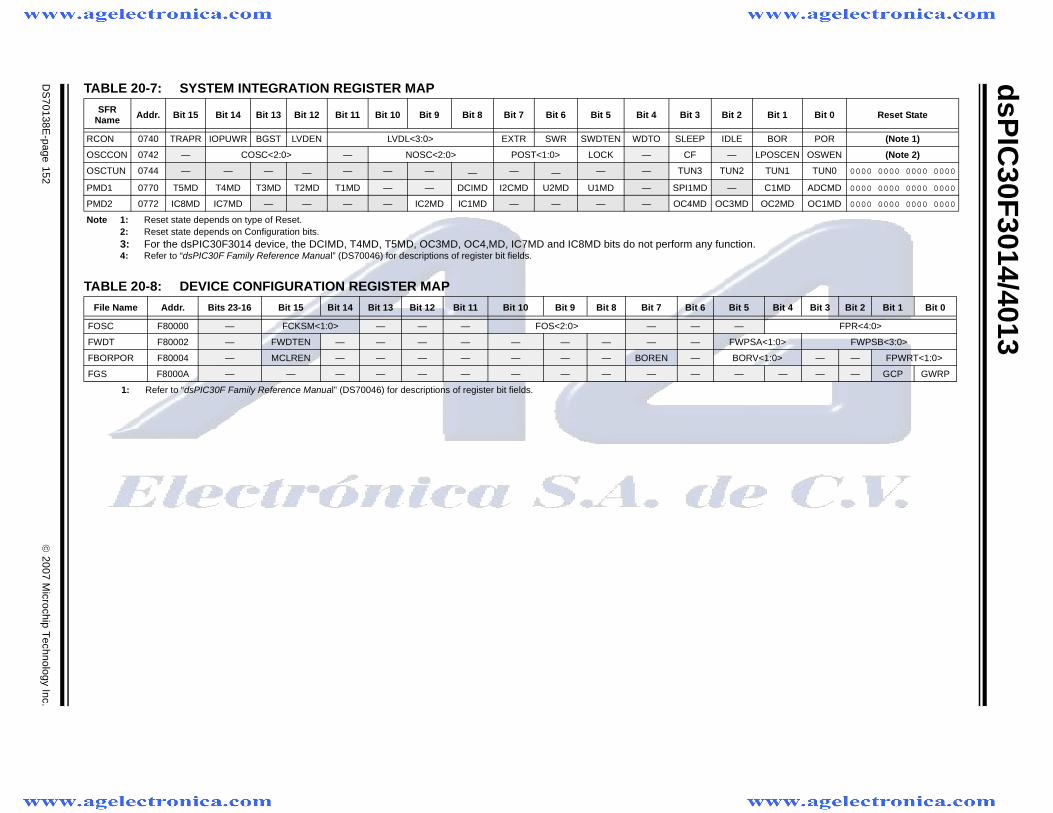
dsP
IC30F
3014/4013
DS
70138E-page 152
© 2007 M
icrochip Technology Inc.
TABLE 20-7: SYSTEM INTEGRATION REGISTER MAP
TABLE 20-8: DEVICE CONFIGURATION REGISTER MAP
SFR Name Addr. Bit 15 Bit 14 Bit 13 Bit 12 Bit 11 Bit 10 Bit 9 Bit 8 Bit 7 Bit 6 Bit 5 Bit 4 Bit 3 Bit 2 Bit 1 Bit 0 Reset State
RCON 0740 TRAPR IOPUWR BGST LVDEN LVDL<3:0> EXTR SWR SWDTEN WDTO SLEEP IDLE BOR POR (Note 1)
OSCCON 0742 — COSC<2:0> — NOSC<2:0> POST<1:0> LOCK — CF — LPOSCEN OSWEN (Note 2)
OSCTUN 0744 — — — — — — — — — — — — TUN3 TUN2 TUN1 TUN0 0000 0000 0000 0000
PMD1 0770 T5MD T4MD T3MD T2MD T1MD — — DCIMD I2CMD U2MD U1MD — SPI1MD — C1MD ADCMD 0000 0000 0000 0000
PMD2 0772 IC8MD IC7MD — — — — IC2MD IC1MD — — — — OC4MD OC3MD OC2MD OC1MD 0000 0000 0000 0000
Note 1: Reset state depends on type of Reset.2: Reset state depends on Configuration bits.3: For the dsPIC30F3014 device, the DCIMD, T4MD, T5MD, OC3MD, OC4,MD, IC7MD and IC8MD bits do not perform any function.4: Refer to “dsPIC30F Family Reference Manual” (DS70046) for descriptions of register bit fields.
File Name Addr. Bits 23-16 Bit 15 Bit 14 Bit 13 Bit 12 Bit 11 Bit 10 Bit 9 Bit 8 Bit 7 Bit 6 Bit 5 Bit 4 Bit 3 Bit 2 Bit 1 Bit 0
FOSC F80000 — FCKSM<1:0> — — — FOS<2:0> — — — FPR<4:0>
FWDT F80002 — FWDTEN — — — — — — — — — FWPSA<1:0> FWPSB<3:0>
FBORPOR F80004 — MCLREN — — — — — — — BOREN — BORV<1:0> — — FPWRT<1:0>
FGS F8000A — — — — — — — — — — — — — — — GCP GWRP
1: Refer to “dsPIC30F Family Reference Manual” (DS70046) for descriptions of register bit fields.
© 2007 Microchip Technology Inc. DS70138E-page 153
dsPIC30F3014/4013
21.0 INSTRUCTION SET SUMMARY
The dsPIC30F instruction set adds manyenhancements to the previous PIC® MCU instructionsets, while maintaining an easy migration from PICMCU instruction sets.
Most instructions are a single program memory word(24 bits). Only three instructions require two programmemory locations.
Each single-word instruction is a 24-bit word dividedinto an 8-bit opcode which specifies the instructiontype, and one or more operands which further specifythe operation of the instruction.
The instruction set is highly orthogonal and is groupedinto five basic categories:
• Word or byte-oriented operations• Bit-oriented operations• Literal operations
• DSP operations• Control operations
Table 21-1 shows the general symbols used indescribing the instructions.
The dsPIC30F instruction set summary in Table 21-2lists all the instructions, along with the status flagsaffected by each instruction.
Most word or byte-oriented W register instructions(including barrel shift instructions) have threeoperands:
• The first source operand which is typically a register ‘Wb’ without any address modifier
• The second source operand which is typically a register ‘Ws’ with or without an address modifier
• The destination of the result which is typically a register ‘Wd’ with or without an address modifier
However, word or byte-oriented file register instructionshave two operands:
• The file register specified by the value ‘f’• The destination, which could either be the file
register ‘f’ or the W0 register, which is denoted as ‘WREG’
Most bit-oriented instructions (including simple rotate/shift instructions) have two operands:
• The W register (with or without an address modifier) or file register (specified by the value of ‘Ws’ or ‘f’)
• The bit in the W register or file register (specified by a literal value or indirectly by the contents of register ‘Wb’)
The literal instructions that involve data movement mayuse some of the following operands:
• A literal value to be loaded into a W register or file register (specified by the value of ‘k’)
• The W register or file register where the literal value is to be loaded (specified by ‘Wb’ or ‘f’)
However, literal instructions that involve arithmetic orlogical operations use some of the following operands:
• The first source operand which is a register ‘Wb’ without any address modifier
• The second source operand which is a literal value
• The destination of the result (only if not the same as the first source operand) which is typically a register ‘Wd’ with or without an address modifier
The MAC class of DSP instructions may use some of thefollowing operands:
• The accumulator (A or B) to be used (required operand)
• The W registers to be used as the two operands• The X and Y address space prefetch operations• The X and Y address space prefetch destinations
• The accumulator write-back destination
The other DSP instructions do not involve anymultiplication, and may include:
• The accumulator to be used (required)
• The source or destination operand (designated as Wso or Wdo, respectively) with or without an address modifier
• The amount of shift specified by a W register ‘Wn’ or a literal value
The control instructions may use some of the followingoperands:
• A program memory address • The mode of the table read and table write
instructions
All instructions are a single word, except for certaindouble word instructions, which were made doubleword instructions so that all the required information isavailable in these 48 bits. In the second word, the8 MSbs are ‘0’s. If this second word is executed as aninstruction (by itself), it executes as a NOP.
Note: This data sheet summarizes features of this groupof dsPIC30F devices and is not intended to be a completereference source. For more information on the CPU,peripherals, register descriptions and general devicefunctionality, refer to the “dsPIC30F Family ReferenceManual” (DS70046). For more information on the deviceinstruction set and programming, refer to the “dsPIC30F/33F Programmer’s Reference Manual” (DS70157).
dsPIC30F3014/4013
DS70138E-page 154 © 2007 Microchip Technology Inc.
Most single-word instructions are executed in a singleinstruction cycle, unless a conditional test is true orthe program counter is changed as a result of theinstruction. In these cases, the execution takes twoinstruction cycles with the additional instructioncycle(s) executed as a NOP. Notable exceptions are theBRA (unconditional/computed branch), indirect CALL/GOTO, all table reads and writes, and RETURN/RETFIEinstructions, which are single-word instructions but taketwo or three cycles. Certain instructions that involveskipping over the subsequent instruction require either
two or three cycles if the skip is performed, dependingon whether the instruction being skipped is a single-word or two-word instruction. Moreover, double wordmoves require two cycles. The double wordinstructions execute in two instruction cycles.
Note: For more details on the instruction set,refer to the Programmer’s ReferenceManual.
TABLE 21-1: SYMBOLS USED IN OPCODE DESCRIPTIONS
Field Description
#text Means literal defined by “text”
(text) Means “content of text”
[text] Means “the location addressed by text”
{ } Optional field or operation
<n:m> Register bit field
.b Byte mode selection
.d Double Word mode selection
.S Shadow register select
.w Word mode selection (default)
Acc One of two accumulators {A, B}
AWB Accumulator write-back destination address register ∈ {W13, [W13]+=2}
bit4 4-bit bit selection field (used in word addressed instructions) ∈ {0...15}
C, DC, N, OV, Z MCU Status bits: Carry, Digit Carry, Negative, Overflow, Sticky Zero
Expr Absolute address, label or expression (resolved by the linker)
f File register address ∈ {0x0000...0x1FFF}
lit1 1-bit unsigned literal ∈ {0,1}
lit4 4-bit unsigned literal ∈ {0...15}
lit5 5-bit unsigned literal ∈ {0...31}
lit8 8-bit unsigned literal ∈ {0...255}
lit10 10-bit unsigned literal ∈ {0...255} for Byte mode, {0:1023} for Word mode
lit14 14-bit unsigned literal ∈ {0...16384}
lit16 16-bit unsigned literal ∈ {0...65535}
lit23 23-bit unsigned literal ∈ {0...8388608}; LSB must be 0
None Field does not require an entry, may be blank
OA, OB, SA, SB DSP Status bits: AccA Overflow, AccB Overflow, AccA Saturate, AccB Saturate
PC Program Counter
Slit10 10-bit signed literal ∈ {-512...511}
Slit16 16-bit signed literal ∈ {-32768...32767}
Slit6 6-bit signed literal ∈ {-16...16}
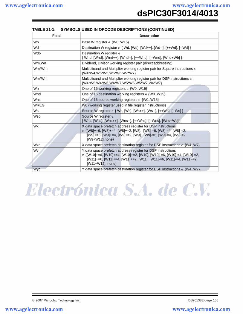
© 2007 Microchip Technology Inc. DS70138E-page 155
dsPIC30F3014/4013
Wb Base W register ∈ {W0..W15}
Wd Destination W register ∈ { Wd, [Wd], [Wd++], [Wd--], [++Wd], [--Wd] }
Wdo Destination W register ∈ { Wnd, [Wnd], [Wnd++], [Wnd--], [++Wnd], [--Wnd], [Wnd+Wb] }
Wm,Wn Dividend, Divisor working register pair (direct addressing)
Wm*Wm Multiplicand and Multiplier working register pair for Square instructions ∈ {W4*W4,W5*W5,W6*W6,W7*W7}
Wm*Wn Multiplicand and Multiplier working register pair for DSP instructions ∈{W4*W5,W4*W6,W4*W7,W5*W6,W5*W7,W6*W7}
Wn One of 16 working registers ∈ {W0..W15}
Wnd One of 16 destination working registers ∈ {W0..W15}
Wns One of 16 source working registers ∈ {W0..W15}
WREG W0 (working register used in file register instructions)
Ws Source W register ∈ { Ws, [Ws], [Ws++], [Ws--], [++Ws], [--Ws] }
Wso Source W register ∈ { Wns, [Wns], [Wns++], [Wns--], [++Wns], [--Wns], [Wns+Wb] }
Wx X data space prefetch address register for DSP instructions ∈ {[W8]+=6, [W8]+=4, [W8]+=2, [W8], [W8]-=6, [W8]-=4, [W8]-=2, [W9]+=6, [W9]+=4, [W9]+=2, [W9], [W9]-=6, [W9]-=4, [W9]-=2, [W9+W12],none}
Wxd X data space prefetch destination register for DSP instructions ∈ {W4..W7}
Wy Y data space prefetch address register for DSP instructions ∈ {[W10]+=6, [W10]+=4, [W10]+=2, [W10], [W10]-=6, [W10]-=4, [W10]-=2, [W11]+=6, [W11]+=4, [W11]+=2, [W11], [W11]-=6, [W11]-=4, [W11]-=2, [W11+W12], none}
Wyd Y data space prefetch destination register for DSP instructions ∈ {W4..W7}
TABLE 21-1: SYMBOLS USED IN OPCODE DESCRIPTIONS (CONTINUED)
Field Description
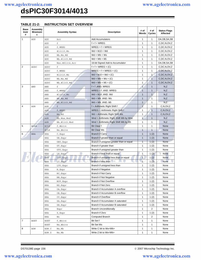
dsPIC30F3014/4013
DS70138E-page 156 © 2007 Microchip Technology Inc.
TABLE 21-2: INSTRUCTION SET OVERVIEW BaseInstr
#
AssemblyMnemoni
cAssembly Syntax Description # of
Words# of
CyclesStatus Flags
Affected
1 ADD ADD Acc Add Accumulators 1 1 OA,OB,SA,SB
ADD f f = f + WREG 1 1 C,DC,N,OV,Z
ADD f,WREG WREG = f + WREG 1 1 C,DC,N,OV,Z
ADD #lit10,Wn Wd = lit10 + Wd 1 1 C,DC,N,OV,Z
ADD Wb,Ws,Wd Wd = Wb + Ws 1 1 C,DC,N,OV,Z
ADD Wb,#lit5,Wd Wd = Wb + lit5 1 1 C,DC,N,OV,Z
ADD Wso,#Slit4,Acc 16-bit Signed Add to Accumulator 1 1 OA,OB,SA,SB
2 ADDC ADDC f f = f + WREG + (C) 1 1 C,DC,N,OV,Z
ADDC f,WREG WREG = f + WREG + (C) 1 1 C,DC,N,OV,Z
ADDC #lit10,Wn Wd = lit10 + Wd + (C) 1 1 C,DC,N,OV,Z
ADDC Wb,Ws,Wd Wd = Wb + Ws + (C) 1 1 C,DC,N,OV,Z
ADDC Wb,#lit5,Wd Wd = Wb + lit5 + (C) 1 1 C,DC,N,OV,Z
3 AND AND f f = f .AND. WREG 1 1 N,Z
AND f,WREG WREG = f .AND. WREG 1 1 N,Z
AND #lit10,Wn Wd = lit10 .AND. Wd 1 1 N,Z
AND Wb,Ws,Wd Wd = Wb .AND. Ws 1 1 N,Z
AND Wb,#lit5,Wd Wd = Wb .AND. lit5 1 1 N,Z
4 ASR ASR f f = Arithmetic Right Shift f 1 1 C,N,OV,Z
ASR f,WREG WREG = Arithmetic Right Shift f 1 1 C,N,OV,Z
ASR Ws,Wd Wd = Arithmetic Right Shift Ws 1 1 C,N,OV,Z
ASR Wb,Wns,Wnd Wnd = Arithmetic Right Shift Wb by Wns 1 1 N,Z
ASR Wb,#lit5,Wnd Wnd = Arithmetic Right Shift Wb by lit5 1 1 N,Z
5 BCLR BCLR f,#bit4 Bit Clear f 1 1 None
BCLR Ws,#bit4 Bit Clear Ws 1 1 None
6 BRA BRA C,Expr Branch if Carry 1 1 (2) None
BRA GE,Expr Branch if greater than or equal 1 1 (2) None
BRA GEU,Expr Branch if unsigned greater than or equal 1 1 (2) None
BRA GT,Expr Branch if greater than 1 1 (2) None
BRA GTU,Expr Branch if unsigned greater than 1 1 (2) None
BRA LE,Expr Branch if less than or equal 1 1 (2) None
BRA LEU,Expr Branch if unsigned less than or equal 1 1 (2) None
BRA LT,Expr Branch if less than 1 1 (2) None
BRA LTU,Expr Branch if unsigned less than 1 1 (2) None
BRA N,Expr Branch if Negative 1 1 (2) None
BRA NC,Expr Branch if Not Carry 1 1 (2) None
BRA NN,Expr Branch if Not Negative 1 1 (2) None
BRA NOV,Expr Branch if Not Overflow 1 1 (2) None
BRA NZ,Expr Branch if Not Zero 1 1 (2) None
BRA OA,Expr Branch if Accumulator A overflow 1 1 (2) None
BRA OB,Expr Branch if Accumulator B overflow 1 1 (2) None
BRA OV,Expr Branch if Overflow 1 1 (2) None
BRA SA,Expr Branch if Accumulator A saturated 1 1 (2) None
BRA SB,Expr Branch if Accumulator B saturated 1 1 (2) None
BRA Expr Branch Unconditionally 1 2 None
BRA Z,Expr Branch if Zero 1 1 (2) None
BRA Wn Computed Branch 1 2 None
7 BSET BSET f,#bit4 Bit Set f 1 1 None
BSET Ws,#bit4 Bit Set Ws 1 1 None
8 BSW BSW.C Ws,Wb Write C bit to Ws<Wb> 1 1 None
BSW.Z Ws,Wb Write Z bit to Ws<Wb> 1 1 None
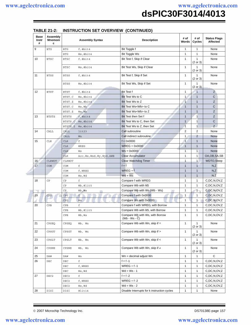
© 2007 Microchip Technology Inc. DS70138E-page 157
dsPIC30F3014/4013
9 BTG BTG f,#bit4 Bit Toggle f 1 1 None
BTG Ws,#bit4 Bit Toggle Ws 1 1 None
10 BTSC BTSC f,#bit4 Bit Test f, Skip if Clear 1 1 (2 or 3)
None
BTSC Ws,#bit4 Bit Test Ws, Skip if Clear 1 1 (2 or 3)
None
11 BTSS BTSS f,#bit4 Bit Test f, Skip if Set 1 1 (2 or 3)
None
BTSS Ws,#bit4 Bit Test Ws, Skip if Set 1 1 (2 or 3)
None
12 BTST BTST f,#bit4 Bit Test f 1 1 Z
BTST.C Ws,#bit4 Bit Test Ws to C 1 1 C
BTST.Z Ws,#bit4 Bit Test Ws to Z 1 1 Z
BTST.C Ws,Wb Bit Test Ws<Wb> to C 1 1 C
BTST.Z Ws,Wb Bit Test Ws<Wb> to Z 1 1 Z
13 BTSTS BTSTS f,#bit4 Bit Test then Set f 1 1 Z
BTSTS.C Ws,#bit4 Bit Test Ws to C, then Set 1 1 C
BTSTS.Z Ws,#bit4 Bit Test Ws to Z, then Set 1 1 Z
14 CALL CALL lit23 Call subroutine 2 2 None
CALL Wn Call indirect subroutine 1 2 None
15 CLR CLR f f = 0x0000 1 1 None
CLR WREG WREG = 0x0000 1 1 None
CLR Ws Ws = 0x0000 1 1 None
CLR Acc,Wx,Wxd,Wy,Wyd,AWB Clear Accumulator 1 1 OA,OB,SA,SB
16 CLRWDT CLRWDT Clear Watchdog Timer 1 1 WDTO,Sleep
17 COM COM f f = f 1 1 N,Z
COM f,WREG WREG = f 1 1 N,Z
COM Ws,Wd Wd = Ws 1 1 N,Z
18 CP CP f Compare f with WREG 1 1 C,DC,N,OV,Z
CP Wb,#lit5 Compare Wb with lit5 1 1 C,DC,N,OV,Z
CP Wb,Ws Compare Wb with Ws (Wb - Ws) 1 1 C,DC,N,OV,Z
19 CP0 CP0 f Compare f with 0x0000 1 1 C,DC,N,OV,Z
CP0 Ws Compare Ws with 0x0000 1 1 C,DC,N,OV,Z
20 CPB CPB f Compare f with WREG, with Borrow 1 1 C,DC,N,OV,Z
CPB Wb,#lit5 Compare Wb with lit5, with Borrow 1 1 C,DC,N,OV,Z
CPB Wb,Ws Compare Wb with Ws, with Borrow (Wb - Ws - C)
1 1 C,DC,N,OV,Z
21 CPSEQ CPSEQ Wb, Wn Compare Wb with Wn, skip if = 1 1 (2 or 3)
None
22 CPSGT CPSGT Wb, Wn Compare Wb with Wn, skip if > 1 1 (2 or 3)
None
23 CPSLT CPSLT Wb, Wn Compare Wb with Wn, skip if < 1 1 (2 or 3)
None
24 CPSNE CPSNE Wb, Wn Compare Wb with Wn, skip if ≠ 1 1 (2 or 3)
None
25 DAW DAW Wn Wn = decimal adjust Wn 1 1 C
26 DEC DEC f f = f -1 1 1 C,DC,N,OV,Z
DEC f,WREG WREG = f -1 1 1 C,DC,N,OV,Z
DEC Ws,Wd Wd = Ws - 1 1 1 C,DC,N,OV,Z
27 DEC2 DEC2 f f = f -2 1 1 C,DC,N,OV,Z
DEC2 f,WREG WREG = f -2 1 1 C,DC,N,OV,Z
DEC2 Ws,Wd Wd = Ws - 2 1 1 C,DC,N,OV,Z
28 DISI DISI #lit14 Disable Interrupts for k instruction cycles 1 1 None
TABLE 21-2: INSTRUCTION SET OVERVIEW (CONTINUED) BaseInstr
#
AssemblyMnemoni
cAssembly Syntax Description # of
Words# of
CyclesStatus Flags
Affected
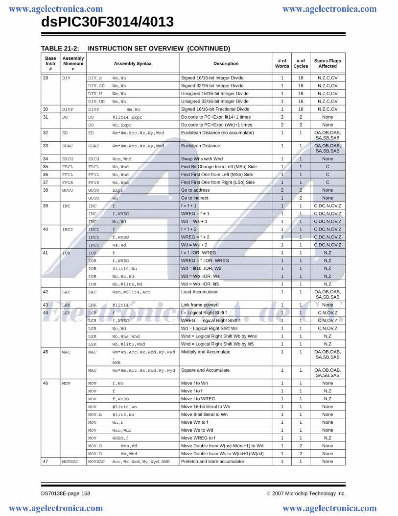
dsPIC30F3014/4013
DS70138E-page 158 © 2007 Microchip Technology Inc.
29 DIV DIV.S Wm,Wn Signed 16/16-bit Integer Divide 1 18 N,Z,C,OV
DIV.SD Wm,Wn Signed 32/16-bit Integer Divide 1 18 N,Z,C,OV
DIV.U Wm,Wn Unsigned 16/16-bit Integer Divide 1 18 N,Z,C,OV
DIV.UD Wm,Wn Unsigned 32/16-bit Integer Divide 1 18 N,Z,C,OV
30 DIVF DIVF Wm,Wn Signed 16/16-bit Fractional Divide 1 18 N,Z,C,OV
31 DO DO #lit14,Expr Do code to PC+Expr, lit14+1 times 2 2 None
DO Wn,Expr Do code to PC+Expr, (Wn)+1 times 2 2 None
32 ED ED Wm*Wm,Acc,Wx,Wy,Wxd Euclidean Distance (no accumulate) 1 1 OA,OB,OAB,SA,SB,SAB
33 EDAC EDAC Wm*Wm,Acc,Wx,Wy,Wxd Euclidean Distance 1 1 OA,OB,OAB,SA,SB,SAB
34 EXCH EXCH Wns,Wnd Swap Wns with Wnd 1 1 None
35 FBCL FBCL Ws,Wnd Find Bit Change from Left (MSb) Side 1 1 C
36 FF1L FF1L Ws,Wnd Find First One from Left (MSb) Side 1 1 C
37 FF1R FF1R Ws,Wnd Find First One from Right (LSb) Side 1 1 C
38 GOTO GOTO Expr Go to address 2 2 None
GOTO Wn Go to indirect 1 2 None
39 INC INC f f = f + 1 1 1 C,DC,N,OV,Z
INC f,WREG WREG = f + 1 1 1 C,DC,N,OV,Z
INC Ws,Wd Wd = Ws + 1 1 1 C,DC,N,OV,Z
40 INC2 INC2 f f = f + 2 1 1 C,DC,N,OV,Z
INC2 f,WREG WREG = f + 2 1 1 C,DC,N,OV,Z
INC2 Ws,Wd Wd = Ws + 2 1 1 C,DC,N,OV,Z
41 IOR IOR f f = f .IOR. WREG 1 1 N,Z
IOR f,WREG WREG = f .IOR. WREG 1 1 N,Z
IOR #lit10,Wn Wd = lit10 .IOR. Wd 1 1 N,Z
IOR Wb,Ws,Wd Wd = Wb .IOR. Ws 1 1 N,Z
IOR Wb,#lit5,Wd Wd = Wb .IOR. lit5 1 1 N,Z
42 LAC LAC Wso,#Slit4,Acc Load Accumulator 1 1 OA,OB,OAB,SA,SB,SAB
43 LNK LNK #lit14 Link frame pointer 1 1 None
44 LSR LSR f f = Logical Right Shift f 1 1 C,N,OV,Z
LSR f,WREG WREG = Logical Right Shift f 1 1 C,N,OV,Z
LSR Ws,Wd Wd = Logical Right Shift Ws 1 1 C,N,OV,Z
LSR Wb,Wns,Wnd Wnd = Logical Right Shift Wb by Wns 1 1 N,Z
LSR Wb,#lit5,Wnd Wnd = Logical Right Shift Wb by lit5 1 1 N,Z
45 MAC MAC Wm*Wn,Acc,Wx,Wxd,Wy,Wyd,AWB
Multiply and Accumulate 1 1 OA,OB,OAB,SA,SB,SAB
MAC Wm*Wm,Acc,Wx,Wxd,Wy,Wyd Square and Accumulate 1 1 OA,OB,OAB,SA,SB,SAB
46 MOV MOV f,Wn Move f to Wn 1 1 None
MOV f Move f to f 1 1 N,Z
MOV f,WREG Move f to WREG 1 1 N,Z
MOV #lit16,Wn Move 16-bit literal to Wn 1 1 None
MOV.b #lit8,Wn Move 8-bit literal to Wn 1 1 None
MOV Wn,f Move Wn to f 1 1 None
MOV Wso,Wdo Move Ws to Wd 1 1 None
MOV WREG,f Move WREG to f 1 1 N,Z
MOV.D Wns,Wd Move Double from W(ns):W(ns+1) to Wd 1 2 None
MOV.D Ws,Wnd Move Double from Ws to W(nd+1):W(nd) 1 2 None
47 MOVSAC MOVSAC Acc,Wx,Wxd,Wy,Wyd,AWB Prefetch and store accumulator 1 1 None
TABLE 21-2: INSTRUCTION SET OVERVIEW (CONTINUED) BaseInstr
#
AssemblyMnemoni
cAssembly Syntax Description # of
Words# of
CyclesStatus Flags
Affected
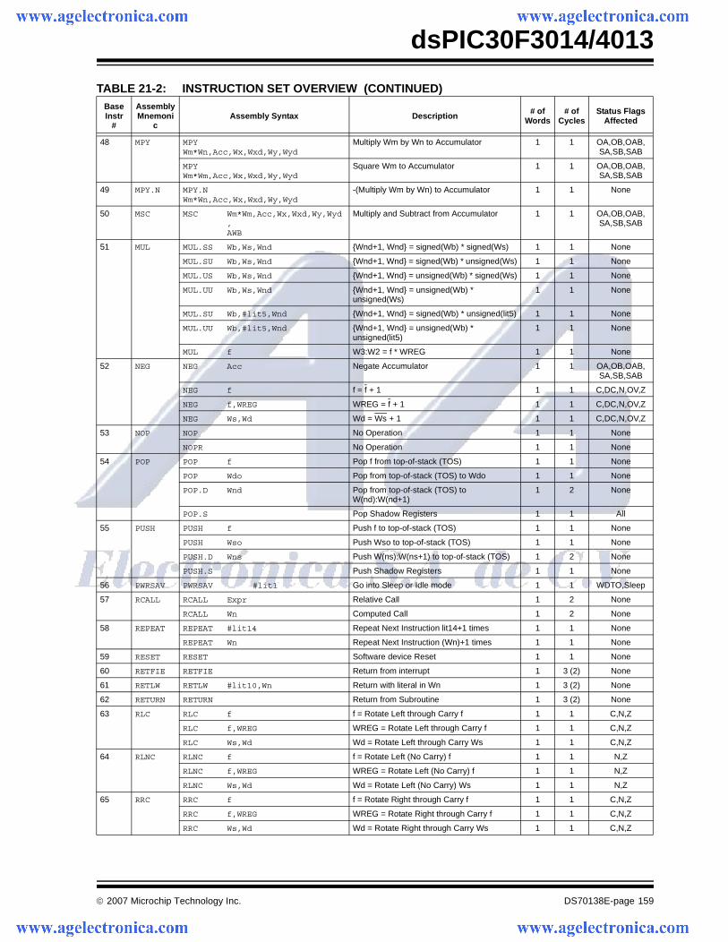
© 2007 Microchip Technology Inc. DS70138E-page 159
dsPIC30F3014/4013
48 MPY MPY Wm*Wn,Acc,Wx,Wxd,Wy,Wyd
Multiply Wm by Wn to Accumulator 1 1 OA,OB,OAB,SA,SB,SAB
MPY Wm*Wm,Acc,Wx,Wxd,Wy,Wyd
Square Wm to Accumulator 1 1 OA,OB,OAB,SA,SB,SAB
49 MPY.N MPY.N Wm*Wn,Acc,Wx,Wxd,Wy,Wyd
-(Multiply Wm by Wn) to Accumulator 1 1 None
50 MSC MSC Wm*Wm,Acc,Wx,Wxd,Wy,Wyd,AWB
Multiply and Subtract from Accumulator 1 1 OA,OB,OAB,SA,SB,SAB
51 MUL MUL.SS Wb,Ws,Wnd {Wnd+1, Wnd} = signed(Wb) * signed(Ws) 1 1 None
MUL.SU Wb,Ws,Wnd {Wnd+1, Wnd} = signed(Wb) * unsigned(Ws) 1 1 None
MUL.US Wb,Ws,Wnd {Wnd+1, Wnd} = unsigned(Wb) * signed(Ws) 1 1 None
MUL.UU Wb,Ws,Wnd {Wnd+1, Wnd} = unsigned(Wb) * unsigned(Ws)
1 1 None
MUL.SU Wb,#lit5,Wnd {Wnd+1, Wnd} = signed(Wb) * unsigned(lit5) 1 1 None
MUL.UU Wb,#lit5,Wnd {Wnd+1, Wnd} = unsigned(Wb) * unsigned(lit5)
1 1 None
MUL f W3:W2 = f * WREG 1 1 None
52 NEG NEG Acc Negate Accumulator 1 1 OA,OB,OAB,SA,SB,SAB
NEG f f = f + 1 1 1 C,DC,N,OV,Z
NEG f,WREG WREG = f + 1 1 1 C,DC,N,OV,Z
NEG Ws,Wd Wd = Ws + 1 1 1 C,DC,N,OV,Z
53 NOP NOP No Operation 1 1 None
NOPR No Operation 1 1 None
54 POP POP f Pop f from top-of-stack (TOS) 1 1 None
POP Wdo Pop from top-of-stack (TOS) to Wdo 1 1 None
POP.D Wnd Pop from top-of-stack (TOS) to W(nd):W(nd+1)
1 2 None
POP.S Pop Shadow Registers 1 1 All
55 PUSH PUSH f Push f to top-of-stack (TOS) 1 1 None
PUSH Wso Push Wso to top-of-stack (TOS) 1 1 None
PUSH.D Wns Push W(ns):W(ns+1) to top-of-stack (TOS) 1 2 None
PUSH.S Push Shadow Registers 1 1 None
56 PWRSAV PWRSAV #lit1 Go into Sleep or Idle mode 1 1 WDTO,Sleep
57 RCALL RCALL Expr Relative Call 1 2 None
RCALL Wn Computed Call 1 2 None
58 REPEAT REPEAT #lit14 Repeat Next Instruction lit14+1 times 1 1 None
REPEAT Wn Repeat Next Instruction (Wn)+1 times 1 1 None
59 RESET RESET Software device Reset 1 1 None
60 RETFIE RETFIE Return from interrupt 1 3 (2) None
61 RETLW RETLW #lit10,Wn Return with literal in Wn 1 3 (2) None
62 RETURN RETURN Return from Subroutine 1 3 (2) None
63 RLC RLC f f = Rotate Left through Carry f 1 1 C,N,Z
RLC f,WREG WREG = Rotate Left through Carry f 1 1 C,N,Z
RLC Ws,Wd Wd = Rotate Left through Carry Ws 1 1 C,N,Z
64 RLNC RLNC f f = Rotate Left (No Carry) f 1 1 N,Z
RLNC f,WREG WREG = Rotate Left (No Carry) f 1 1 N,Z
RLNC Ws,Wd Wd = Rotate Left (No Carry) Ws 1 1 N,Z
65 RRC RRC f f = Rotate Right through Carry f 1 1 C,N,Z
RRC f,WREG WREG = Rotate Right through Carry f 1 1 C,N,Z
RRC Ws,Wd Wd = Rotate Right through Carry Ws 1 1 C,N,Z
TABLE 21-2: INSTRUCTION SET OVERVIEW (CONTINUED) BaseInstr
#
AssemblyMnemoni
cAssembly Syntax Description # of
Words# of
CyclesStatus Flags
Affected
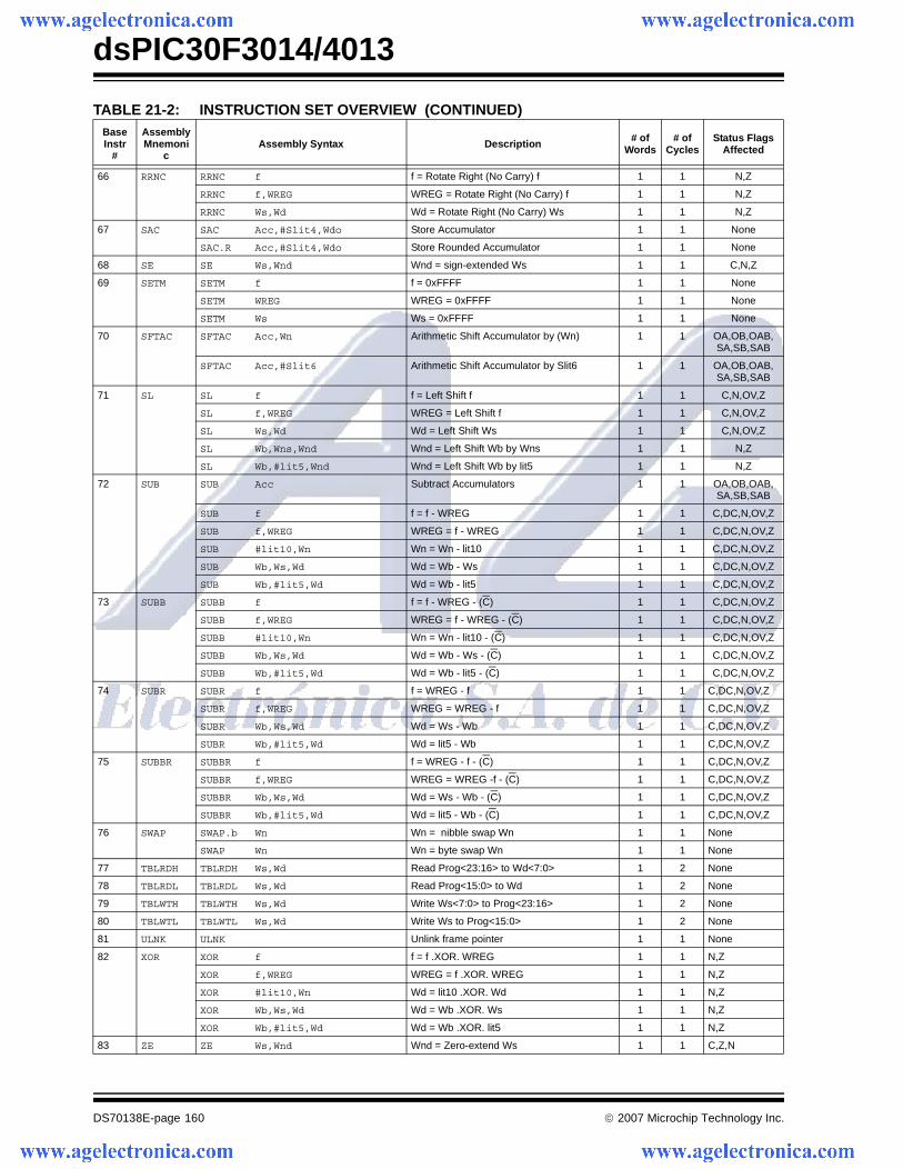
dsPIC30F3014/4013
DS70138E-page 160 © 2007 Microchip Technology Inc.
66 RRNC RRNC f f = Rotate Right (No Carry) f 1 1 N,Z
RRNC f,WREG WREG = Rotate Right (No Carry) f 1 1 N,Z
RRNC Ws,Wd Wd = Rotate Right (No Carry) Ws 1 1 N,Z
67 SAC SAC Acc,#Slit4,Wdo Store Accumulator 1 1 None
SAC.R Acc,#Slit4,Wdo Store Rounded Accumulator 1 1 None
68 SE SE Ws,Wnd Wnd = sign-extended Ws 1 1 C,N,Z
69 SETM SETM f f = 0xFFFF 1 1 None
SETM WREG WREG = 0xFFFF 1 1 None
SETM Ws Ws = 0xFFFF 1 1 None
70 SFTAC SFTAC Acc,Wn Arithmetic Shift Accumulator by (Wn) 1 1 OA,OB,OAB,SA,SB,SAB
SFTAC Acc,#Slit6 Arithmetic Shift Accumulator by Slit6 1 1 OA,OB,OAB,SA,SB,SAB
71 SL SL f f = Left Shift f 1 1 C,N,OV,Z
SL f,WREG WREG = Left Shift f 1 1 C,N,OV,Z
SL Ws,Wd Wd = Left Shift Ws 1 1 C,N,OV,Z
SL Wb,Wns,Wnd Wnd = Left Shift Wb by Wns 1 1 N,Z
SL Wb,#lit5,Wnd Wnd = Left Shift Wb by lit5 1 1 N,Z
72 SUB SUB Acc Subtract Accumulators 1 1 OA,OB,OAB,SA,SB,SAB
SUB f f = f - WREG 1 1 C,DC,N,OV,Z
SUB f,WREG WREG = f - WREG 1 1 C,DC,N,OV,Z
SUB #lit10,Wn Wn = Wn - lit10 1 1 C,DC,N,OV,Z
SUB Wb,Ws,Wd Wd = Wb - Ws 1 1 C,DC,N,OV,Z
SUB Wb,#lit5,Wd Wd = Wb - lit5 1 1 C,DC,N,OV,Z
73 SUBB SUBB f f = f - WREG - (C) 1 1 C,DC,N,OV,Z
SUBB f,WREG WREG = f - WREG - (C) 1 1 C,DC,N,OV,Z
SUBB #lit10,Wn Wn = Wn - lit10 - (C) 1 1 C,DC,N,OV,Z
SUBB Wb,Ws,Wd Wd = Wb - Ws - (C) 1 1 C,DC,N,OV,Z
SUBB Wb,#lit5,Wd Wd = Wb - lit5 - (C) 1 1 C,DC,N,OV,Z
74 SUBR SUBR f f = WREG - f 1 1 C,DC,N,OV,Z
SUBR f,WREG WREG = WREG - f 1 1 C,DC,N,OV,Z
SUBR Wb,Ws,Wd Wd = Ws - Wb 1 1 C,DC,N,OV,Z
SUBR Wb,#lit5,Wd Wd = lit5 - Wb 1 1 C,DC,N,OV,Z
75 SUBBR SUBBR f f = WREG - f - (C) 1 1 C,DC,N,OV,Z
SUBBR f,WREG WREG = WREG -f - (C) 1 1 C,DC,N,OV,Z
SUBBR Wb,Ws,Wd Wd = Ws - Wb - (C) 1 1 C,DC,N,OV,Z
SUBBR Wb,#lit5,Wd Wd = lit5 - Wb - (C) 1 1 C,DC,N,OV,Z
76 SWAP SWAP.b Wn Wn = nibble swap Wn 1 1 None
SWAP Wn Wn = byte swap Wn 1 1 None
77 TBLRDH TBLRDH Ws,Wd Read Prog<23:16> to Wd<7:0> 1 2 None
78 TBLRDL TBLRDL Ws,Wd Read Prog<15:0> to Wd 1 2 None
79 TBLWTH TBLWTH Ws,Wd Write Ws<7:0> to Prog<23:16> 1 2 None
80 TBLWTL TBLWTL Ws,Wd Write Ws to Prog<15:0> 1 2 None
81 ULNK ULNK Unlink frame pointer 1 1 None
82 XOR XOR f f = f .XOR. WREG 1 1 N,Z
XOR f,WREG WREG = f .XOR. WREG 1 1 N,Z
XOR #lit10,Wn Wd = lit10 .XOR. Wd 1 1 N,Z
XOR Wb,Ws,Wd Wd = Wb .XOR. Ws 1 1 N,Z
XOR Wb,#lit5,Wd Wd = Wb .XOR. lit5 1 1 N,Z
83 ZE ZE Ws,Wnd Wnd = Zero-extend Ws 1 1 C,Z,N
TABLE 21-2: INSTRUCTION SET OVERVIEW (CONTINUED) BaseInstr
#
AssemblyMnemoni
cAssembly Syntax Description # of
Words# of
CyclesStatus Flags
Affected
© 2007 Microchip Technology Inc. DS70138E-page 161
dsPIC30F3014/4013
22.0 DEVELOPMENT SUPPORT
The PIC® microcontrollers are supported with a fullrange of hardware and software development tools:
• Integrated Development Environment
- MPLAB® IDE Software• Assemblers/Compilers/Linkers
- MPASMTM Assembler
- MPLAB C18 and MPLAB C30 C Compilers- MPLINKTM Object Linker/
MPLIBTM Object Librarian- MPLAB ASM30 Assembler/Linker/Library
• Simulators
- MPLAB SIM Software Simulator• Emulators
- MPLAB ICE 2000 In-Circuit Emulator
- MPLAB ICE 4000 In-Circuit Emulator• In-Circuit Debugger
- MPLAB ICD 2
• Device Programmers- PICSTART® Plus Development Programmer- MPLAB PM3 Device Programmer
- PICkit™ 2 Development Programmer• Low-Cost Demonstration and Development
Boards and Evaluation Kits
22.1 MPLAB Integrated Development Environment Software
The MPLAB IDE software brings an ease of softwaredevelopment previously unseen in the 8/16-bit micro-controller market. The MPLAB IDE is a Windows®
operating system-based application that contains:
• A single graphical interface to all debugging tools- Simulator- Programmer (sold separately)
- Emulator (sold separately)- In-Circuit Debugger (sold separately)
• A full-featured editor with color-coded context
• A multiple project manager• Customizable data windows with direct edit of
contents• High-level source code debugging• Visual device initializer for easy register
initialization• Mouse over variable inspection
• Drag and drop variables from source to watch windows
• Extensive on-line help• Integration of select third party tools, such as
HI-TECH Software C Compilers and IAR C Compilers
The MPLAB IDE allows you to:
• Edit your source files (either assembly or C)
• One touch assemble (or compile) and download to PIC MCU emulator and simulator tools (automatically updates all project information)
• Debug using:
- Source files (assembly or C)- Mixed assembly and C- Machine code
MPLAB IDE supports multiple debugging tools in asingle development paradigm, from the cost-effectivesimulators, through low-cost in-circuit debuggers, tofull-featured emulators. This eliminates the learningcurve when upgrading to tools with increased flexibilityand power.
dsPIC30F3014/4013
DS70138E-page 162 © 2007 Microchip Technology Inc.
22.2 MPASM Assembler
The MPASM Assembler is a full-featured, universalmacro assembler for all PIC MCUs.
The MPASM Assembler generates relocatable objectfiles for the MPLINK Object Linker, Intel® standard HEXfiles, MAP files to detail memory usage and symbolreference, absolute LST files that contain source linesand generated machine code and COFF files fordebugging.
The MPASM Assembler features include:
• Integration into MPLAB IDE projects
• User-defined macros to streamline assembly code
• Conditional assembly for multi-purpose source files
• Directives that allow complete control over the assembly process
22.3 MPLAB C18 and MPLAB C30 C Compilers
The MPLAB C18 and MPLAB C30 Code DevelopmentSystems are complete ANSI C compilers forMicrochip’s PIC18 family of microcontrollers and thedsPIC30, dsPIC33 and PIC24 family of digital signalcontrollers. These compilers provide powerful integra-tion capabilities, superior code optimization and easeof use not found with other compilers.
For easy source level debugging, the compilers providesymbol information that is optimized to the MPLAB IDEdebugger.
22.4 MPLINK Object Linker/MPLIB Object Librarian
The MPLINK Object Linker combines relocatableobjects created by the MPASM Assembler and theMPLAB C18 C Compiler. It can link relocatable objectsfrom precompiled libraries, using directives from alinker script.
The MPLIB Object Librarian manages the creation andmodification of library files of precompiled code. Whena routine from a library is called from a source file, onlythe modules that contain that routine are linked in withthe application. This allows large libraries to be usedefficiently in many different applications.
The object linker/library features include:
• Efficient linking of single libraries instead of many smaller files
• Enhanced code maintainability by grouping related modules together
• Flexible creation of libraries with easy module listing, replacement, deletion and extraction
22.5 MPLAB ASM30 Assembler, Linker and Librarian
MPLAB ASM30 Assembler produces relocatablemachine code from symbolic assembly language fordsPIC30F devices. MPLAB C30 C Compiler uses theassembler to produce its object file. The assemblergenerates relocatable object files that can then bearchived or linked with other relocatable object files andarchives to create an executable file. Notable featuresof the assembler include:
• Support for the entire dsPIC30F instruction set
• Support for fixed-point and floating-point data• Command line interface• Rich directive set
• Flexible macro language• MPLAB IDE compatibility
22.6 MPLAB SIM Software Simulator
The MPLAB SIM Software Simulator allows codedevelopment in a PC-hosted environment by simulat-ing the PIC MCUs and dsPIC® DSCs on an instructionlevel. On any given instruction, the data areas can beexamined or modified and stimuli can be applied froma comprehensive stimulus controller. Registers can belogged to files for further run-time analysis. The tracebuffer and logic analyzer display extend the power ofthe simulator to record and track program execution,actions on I/O, most peripherals and internal registers.
The MPLAB SIM Software Simulator fully supportssymbolic debugging using the MPLAB C18 andMPLAB C30 C Compilers, and the MPASM andMPLAB ASM30 Assemblers. The software simulatoroffers the flexibility to develop and debug code outsideof the hardware laboratory environment, making it anexcellent, economical software development tool.
© 2007 Microchip Technology Inc. DS70138E-page 163
dsPIC30F3014/4013
22.7 MPLAB ICE 2000 High-Performance In-Circuit Emulator
The MPLAB ICE 2000 In-Circuit Emulator is intendedto provide the product development engineer with acomplete microcontroller design tool set for PIC micro-controllers. Software control of the MPLAB ICE 2000In-Circuit Emulator is advanced by the MPLAB Integrated Development Environment, which allowsediting, building, downloading and source debuggingfrom a single environment.
The MPLAB ICE 2000 is a full-featured emulatorsystem with enhanced trace, trigger and data monitor-ing features. Interchangeable processor modules allowthe system to be easily reconfigured for emulation ofdifferent processors. The architecture of the MPLABICE 2000 In-Circuit Emulator allows expansion tosupport new PIC microcontrollers.
The MPLAB ICE 2000 In-Circuit Emulator system hasbeen designed as a real-time emulation system withadvanced features that are typically found on moreexpensive development tools. The PC platform andMicrosoft® Windows® 32-bit operating system werechosen to best make these features available in asimple, unified application.
22.8 MPLAB ICE 4000 High-Performance In-Circuit Emulator
The MPLAB ICE 4000 In-Circuit Emulator is intended toprovide the product development engineer with acomplete microcontroller design tool set for high-endPIC MCUs and dsPIC DSCs. Software control of theMPLAB ICE 4000 In-Circuit Emulator is provided by theMPLAB Integrated Development Environment, whichallows editing, building, downloading and sourcedebugging from a single environment.
The MPLAB ICE 4000 is a premium emulator system,providing the features of MPLAB ICE 2000, but withincreased emulation memory and high-speed perfor-mance for dsPIC30F and PIC18XXXX devices. Itsadvanced emulator features include complex triggeringand timing, and up to 2 Mb of emulation memory.
The MPLAB ICE 4000 In-Circuit Emulator system hasbeen designed as a real-time emulation system withadvanced features that are typically found on moreexpensive development tools. The PC platform andMicrosoft Windows 32-bit operating system werechosen to best make these features available in asimple, unified application.
22.9 MPLAB ICD 2 In-Circuit Debugger
Microchip’s In-Circuit Debugger, MPLAB ICD 2, is apowerful, low-cost, run-time development tool,connecting to the host PC via an RS-232 or high-speedUSB interface. This tool is based on the Flash PICMCUs and can be used to develop for these and otherPIC MCUs and dsPIC DSCs. The MPLAB ICD 2 utilizesthe in-circuit debugging capability built into the Flashdevices. This feature, along with Microchip’s In-CircuitSerial ProgrammingTM (ICSPTM) protocol, offers cost-effective, in-circuit Flash debugging from the graphicaluser interface of the MPLAB Integrated DevelopmentEnvironment. This enables a designer to develop anddebug source code by setting breakpoints, single step-ping and watching variables, and CPU status andperipheral registers. Running at full speed enablestesting hardware and applications in real time. MPLABICD 2 also serves as a development programmer forselected PIC devices.
22.10 MPLAB PM3 Device Programmer
The MPLAB PM3 Device Programmer is a universal,CE compliant device programmer with programmablevoltage verification at VDDMIN and VDDMAX formaximum reliability. It features a large LCD display(128 x 64) for menus and error messages and a modu-lar, detachable socket assembly to support variouspackage types. The ICSP™ cable assembly is includedas a standard item. In Stand-Alone mode, the MPLABPM3 Device Programmer can read, verify and programPIC devices without a PC connection. It can also setcode protection in this mode. The MPLAB PM3connects to the host PC via an RS-232 or USB cable.The MPLAB PM3 has high-speed communications andoptimized algorithms for quick programming of largememory devices and incorporates an SD/MMC card forfile storage and secure data applications.
dsPIC30F3014/4013
DS70138E-page 164 © 2007 Microchip Technology Inc.
22.11 PICSTART Plus Development Programmer
The PICSTART Plus Development Programmer is aneasy-to-use, low-cost, prototype programmer. Itconnects to the PC via a COM (RS-232) port. MPLABIntegrated Development Environment software makesusing the programmer simple and efficient. ThePICSTART Plus Development Programmer supportsmost PIC devices in DIP packages up to 40 pins.Larger pin count devices, such as the PIC16C92X andPIC17C76X, may be supported with an adapter socket.The PICSTART Plus Development Programmer is CEcompliant.
22.12 PICkit 2 Development Programmer
The PICkit™ 2 Development Programmer is a low-costprogrammer with an easy-to-use interface for pro-gramming many of Microchip’s baseline, mid-rangeand PIC18F families of Flash memory microcontrollers.The PICkit 2 Starter Kit includes a prototyping develop-ment board, twelve sequential lessons, software andHI-TECH’s PICC™ Lite C compiler, and is designed tohelp get up to speed quickly using PIC® micro-controllers. The kit provides everything needed toprogram, evaluate and develop applications usingMicrochip’s powerful, mid-range Flash memory familyof microcontrollers.
22.13 Demonstration, Development and Evaluation Boards
A wide variety of demonstration, development andevaluation boards for various PIC MCUs and dsPICDSCs allows quick application development on fully func-tional systems. Most boards include prototyping areas foradding custom circuitry and provide application firmwareand source code for examination and modification.
The boards support a variety of features, including LEDs,temperature sensors, switches, speakers, RS-232interfaces, LCD displays, potentiometers and additionalEEPROM memory.
The demonstration and development boards can beused in teaching environments, for prototyping customcircuits and for learning about various microcontrollerapplications.
In addition to the PICDEM™ and dsPICDEM™ demon-stration/development board series of circuits, Microchiphas a line of evaluation kits and demonstration softwarefor analog filter design, KEELOQ® security ICs, CAN,IrDA®, PowerSmart® battery management, SEEVAL®
evaluation system, Sigma-Delta ADC, flow ratesensing, plus many more.
Check the Microchip web page (www.microchip.com)and the latest “Product Selector Guide” (DS00148) forthe complete list of demonstration, development andevaluation kits.
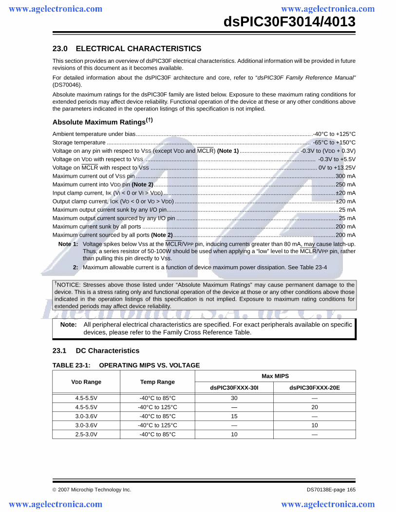
© 2007 Microchip Technology Inc. DS70138E-page 165
dsPIC30F3014/4013
23.0 ELECTRICAL CHARACTERISTICS
This section provides an overview of dsPIC30F electrical characteristics. Additional information will be provided in futurerevisions of this document as it becomes available.
For detailed information about the dsPIC30F architecture and core, refer to “dsPIC30F Family Reference Manual”(DS70046).
Absolute maximum ratings for the dsPIC30F family are listed below. Exposure to these maximum rating conditions forextended periods may affect device reliability. Functional operation of the device at these or any other conditions abovethe parameters indicated in the operation listings of this specification is not implied.
Absolute Maximum Ratings(†)
Ambient temperature under bias............................................................................................................ .-40°C to +125°C
Storage temperature .............................................................................................................................. -65°C to +150°CVoltage on any pin with respect to VSS (except VDD and MCLR) (Note 1) ..................................... -0.3V to (VDD + 0.3V)Voltage on VDD with respect to VSS ......................................................................................................... -0.3V to +5.5V
Voltage on MCLR with respect to VSS ....................................................................................................... 0V to +13.25VMaximum current out of VSS pin ...........................................................................................................................300 mAMaximum current into VDD pin (Note 2)................................................................................................................250 mA
Input clamp current, IIK (VI < 0 or VI > VDD) ..........................................................................................................±20 mAOutput clamp current, IOK (VO < 0 or VO > VDD) ...................................................................................................±20 mAMaximum output current sunk by any I/O pin..........................................................................................................25 mA
Maximum output current sourced by any I/O pin ....................................................................................................25 mAMaximum current sunk by all ports .......................................................................................................................200 mAMaximum current sourced by all ports (Note 2)....................................................................................................200 mA
Note 1: Voltage spikes below Vss at the MCLR/VPP pin, inducing currents greater than 80 mA, may cause latch-up.Thus, a series resistor of 50-100W should be used when applying a “low” level to the MCLR/VPP pin, ratherthan pulling this pin directly to Vss.
2: Maximum allowable current is a function of device maximum power dissipation. See Table 23-4
23.1 DC Characteristics
†NOTICE: Stresses above those listed under “Absolute Maximum Ratings” may cause permanent damage to thedevice. This is a stress rating only and functional operation of the device at those or any other conditions above thoseindicated in the operation listings of this specification is not implied. Exposure to maximum rating conditions forextended periods may affect device reliability.
Note: All peripheral electrical characteristics are specified. For exact peripherals available on specific devices, please refer to the Family Cross Reference Table.
TABLE 23-1: OPERATING MIPS VS. VOLTAGE
VDD Range Temp RangeMax MIPS
dsPIC30FXXX-30I dsPIC30FXXX-20E
4.5-5.5V -40°C to 85°C 30 —
4.5-5.5V -40°C to 125°C — 20
3.0-3.6V -40°C to 85°C 15 —
3.0-3.6V -40°C to 125°C — 10
2.5-3.0V -40°C to 85°C 10 —
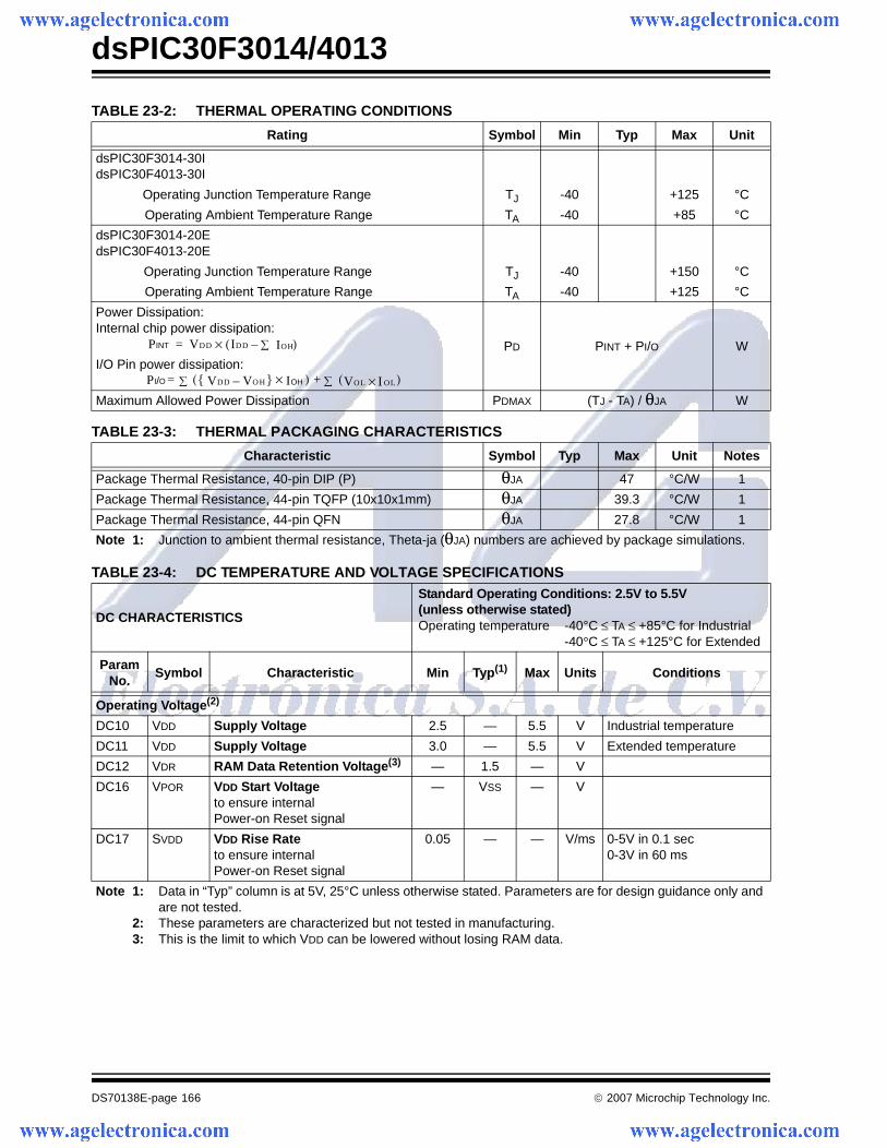
dsPIC30F3014/4013
DS70138E-page 166 © 2007 Microchip Technology Inc.
TABLE 23-2: THERMAL OPERATING CONDITIONS
Rating Symbol Min Typ Max Unit
dsPIC30F3014-30IdsPIC30F4013-30I
Operating Junction Temperature Range TJ -40 +125 °C
Operating Ambient Temperature Range TA -40 +85 °C
dsPIC30F3014-20EdsPIC30F4013-20E
Operating Junction Temperature Range TJ -40 +150 °C
Operating Ambient Temperature Range TA -40 +125 °C
Power Dissipation:Internal chip power dissipation:
PD PINT + PI/O WI/O Pin power dissipation:
Maximum Allowed Power Dissipation PDMAX (TJ - TA) / θJA W
TABLE 23-3: THERMAL PACKAGING CHARACTERISTICS
Characteristic Symbol Typ Max Unit Notes
Package Thermal Resistance, 40-pin DIP (P) θJA 47 °C/W 1
Package Thermal Resistance, 44-pin TQFP (10x10x1mm) θJA 39.3 °C/W 1
Package Thermal Resistance, 44-pin QFN θJA 27.8 °C/W 1
Note 1: Junction to ambient thermal resistance, Theta-ja (θJA) numbers are achieved by package simulations.
TABLE 23-4: DC TEMPERATURE AND VOLTAGE SPECIFICATIONS
DC CHARACTERISTICS
Standard Operating Conditions: 2.5V to 5.5V(unless otherwise stated)Operating temperature -40°C ≤ TA ≤ +85°C for Industrial
-40°C ≤ TA ≤ +125°C for Extended
Param No.
Symbol Characteristic Min Typ(1) Max Units Conditions
Operating Voltage(2)
DC10 VDD Supply Voltage 2.5 — 5.5 V Industrial temperature
DC11 VDD Supply Voltage 3.0 — 5.5 V Extended temperature
DC12 VDR RAM Data Retention Voltage(3) — 1.5 — V
DC16 VPOR VDD Start Voltageto ensure internalPower-on Reset signal
— VSS — V
DC17 SVDD VDD Rise Rateto ensure internalPower-on Reset signal
0.05 — — V/ms 0-5V in 0.1 sec0-3V in 60 ms
Note 1: Data in “Typ” column is at 5V, 25°C unless otherwise stated. Parameters are for design guidance only and are not tested.
2: These parameters are characterized but not tested in manufacturing.3: This is the limit to which VDD can be lowered without losing RAM data.
PINT VDD IDD IOH∑–( )×=
PI/O VDD VO H–{ } IOH×( )∑ VOL I OL×( )∑+=
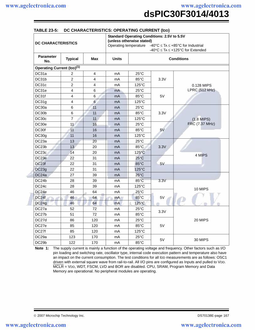
© 2007 Microchip Technology Inc. DS70138E-page 167
dsPIC30F3014/4013
TABLE 23-5: DC CHARACTERISTICS: OPERATING CURRENT (IDD)
DC CHARACTERISTICS
Standard Operating Conditions: 2.5V to 5.5V(unless otherwise stated)Operating temperature -40°C ≤ TA ≤ +85°C for Industrial
-40°C ≤ TA ≤ +125°C for Extended
Parameter No.
Typical Max Units Conditions
Operating Current (IDD)(1)
DC31a 2 4 mA 25°C
3.3V
0.128 MIPSLPRC (512 kHz)
DC31b 2 4 mA 85°C
DC31c 2 4 mA 125°C
DC31e 4 6 mA 25°C
5VDC31f 4 6 mA 85°C
DC31g 4 6 mA 125°C
DC30a 6 11 mA 25°C
3.3V
(1.8 MIPS)FRC (7.37 MHz)
DC30b 6 11 mA 85°C
DC30c 7 11 mA 125°C
DC30e 11 16 mA 25°C
5VDC30f 11 16 mA 85°C
DC30g 11 16 mA 125°C
DC23a 13 20 mA 25°C
3.3V
4 MIPS
DC23b 13 20 mA 85°C
DC23c 14 20 mA 125°C
DC23e 22 31 mA 25°C
5VDC23f 22 31 mA 85°C
DC23g 22 31 mA 125°C
DC24a 27 39 mA 25°C
3.3V
10 MIPS
DC24b 28 39 mA 85°C
DC24c 28 39 mA 125°C
DC24e 46 64 mA 25°C
5VDC24f 46 64 mA 85°C
DC24g 46 64 mA 125°C
DC27a 52 72 mA 25°C3.3V
20 MIPS
DC27b 51 72 mA 85°C
DC27d 86 120 mA 25°C
5VDC27e 85 120 mA 85°C
DC27f 85 120 mA 125°C
DC29a 123 170 mA 25°C5V 30 MIPS
DC29b 122 170 mA 85°C
Note 1: The supply current is mainly a function of the operating voltage and frequency. Other factors such as I/O pin loading and switching rate, oscillator type, internal code execution pattern and temperature also have an impact on the current consumption. The test conditions for all IDD measurements are as follows: OSC1 driven with external square wave from rail-to-rail. All I/O pins are configured as Inputs and pulled to VDD. MCLR = VDD, WDT, FSCM, LVD and BOR are disabled. CPU, SRAM, Program Memory and Data Memory are operational. No peripheral modules are operating.
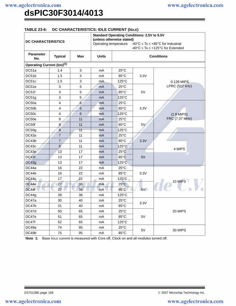
dsPIC30F3014/4013
DS70138E-page 168 © 2007 Microchip Technology Inc.
TABLE 23-6: DC CHARACTERISTICS: IDLE CURRENT (IIDLE)
DC CHARACTERISTICS
Standard Operating Conditions: 2.5V to 5.5V(unless otherwise stated)Operating temperature -40°C ≤ TA ≤ +85°C for Industrial
-40°C ≤ TA ≤ +125°C for Extended
Parameter No.
Typical Max Units Conditions
Operating Current (IDD)(1)
DC51a 1.4 3 mA 25°C
3.3V
0.128 MIPSLPRC (512 kHz)
DC51b 1.5 3 mA 85°C
DC51c 1.5 3 mA 125°C
DC51e 3 5 mA 25°C
5VDC51f 3 5 mA 85°C
DC51g 3 5 mA 125°C
DC50a 4 6 mA 25°C
3.3V
(1.8 MIPS)FRC (7.37 MHz)
DC50b 4 6 mA 85°C
DC50c 4 6 mA 125°C
DC50e 8 11 mA 25°C
5VDC50f 8 11 mA 85°C
DC50g 8 11 mA 125°C
DC43a 7 11 mA 25°C
3.3V
4 MIPS
DC43b 7 11 mA 85°C
DC43c 8 11 mA 125°C
DC43e 13 17 mA 25°C
5VDC43f 13 17 mA 85°C
DC43g 13 17 mA 125°C
DC44a 16 22 mA 25°C
3.3V
10 MIPS
DC44b 16 22 mA 85°C
DC44c 17 22 mA 125°C
DC44e 27 36 mA 25°C
5VDC44f 27 36 mA 85°C
DC44g 28 36 mA 125°C
DC47a 30 40 mA 25°C3.3V
20 MIPS
DC47b 31 40 mA 85°C
DC47d 50 65 mA 25°C
5VDC47e 51 65 mA 85°C
DC47f 52 65 mA 125°C
DC49a 74 95 mA 25°C5V 30 MIPS
DC49b 75 95 mA 85°C
Note 1: Base IIDLE current is measured with Core off, Clock on and all modules turned off.
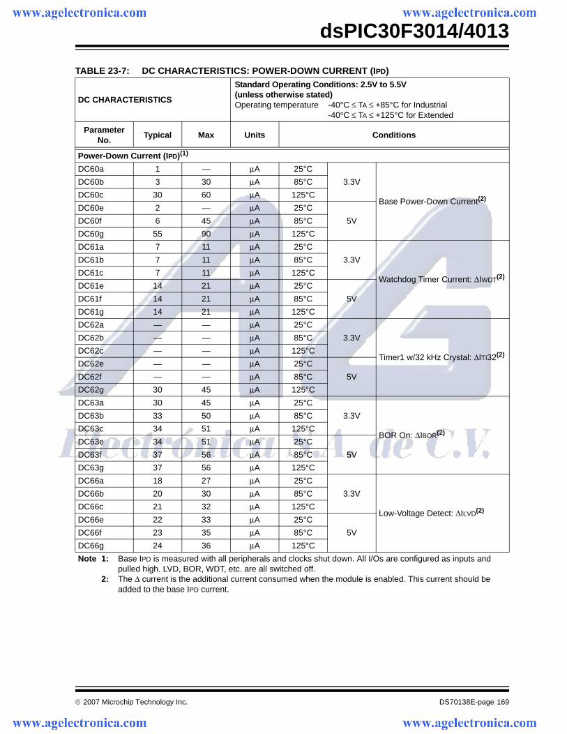
© 2007 Microchip Technology Inc. DS70138E-page 169
dsPIC30F3014/4013
TABLE 23-7: DC CHARACTERISTICS: POWER-DOWN CURRENT (IPD)
DC CHARACTERISTICS
Standard Operating Conditions: 2.5V to 5.5V(unless otherwise stated)Operating temperature -40°C ≤ TA ≤ +85°C for Industrial
-40°C ≤ TA ≤ +125°C for Extended
Parameter No.
Typical Max Units Conditions
Power-Down Current (IPD)(1)
DC60a 1 — μA 25°C
3.3V
Base Power-Down Current(2)
DC60b 3 30 μA 85°C
DC60c 30 60 μA 125°C
DC60e 2 — μA 25°C
5VDC60f 6 45 μA 85°C
DC60g 55 90 μA 125°C
DC61a 7 11 μA 25°C
3.3V
Watchdog Timer Current: ΔIWDT(2)
DC61b 7 11 μA 85°C
DC61c 7 11 μA 125°C
DC61e 14 21 μA 25°C
5VDC61f 14 21 μA 85°C
DC61g 14 21 μA 125°C
DC62a — — μA 25°C
3.3V
Timer1 w/32 kHz Crystal: ΔITI32(2)
DC62b — — μA 85°C
DC62c — — μA 125°C
DC62e — — μA 25°C
5VDC62f — — μA 85°C
DC62g 30 45 μA 125°C
DC63a 30 45 μA 25°C
3.3V
BOR On: ΔIBOR(2)
DC63b 33 50 μA 85°C
DC63c 34 51 μA 125°C
DC63e 34 51 μA 25°C
5VDC63f 37 56 μA 85°C
DC63g 37 56 μA 125°C
DC66a 18 27 μA 25°C
3.3V
Low-Voltage Detect: ΔILVD(2)
DC66b 20 30 μA 85°C
DC66c 21 32 μA 125°C
DC66e 22 33 μA 25°C
5VDC66f 23 35 μA 85°C
DC66g 24 36 μA 125°C
Note 1: Base IPD is measured with all peripherals and clocks shut down. All I/Os are configured as inputs and pulled high. LVD, BOR, WDT, etc. are all switched off.
2: The Δ current is the additional current consumed when the module is enabled. This current should be added to the base IPD current.
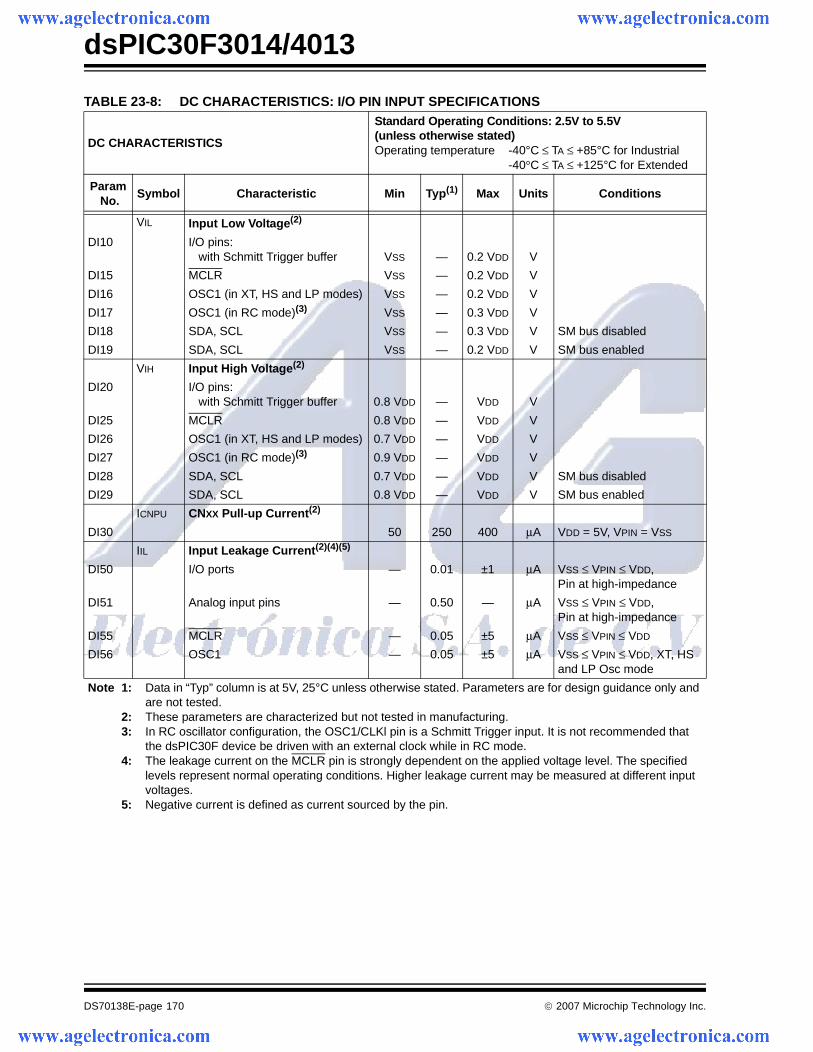
dsPIC30F3014/4013
DS70138E-page 170 © 2007 Microchip Technology Inc.
TABLE 23-8: DC CHARACTERISTICS: I/O PIN INPUT SPECIFICATIONS
DC CHARACTERISTICS
Standard Operating Conditions: 2.5V to 5.5V(unless otherwise stated)Operating temperature -40°C ≤ TA ≤ +85°C for Industrial
-40°C ≤ TA ≤ +125°C for Extended
Param No.
Symbol Characteristic Min Typ(1) Max Units Conditions
VIL Input Low Voltage(2)
DI10 I/O pins: with Schmitt Trigger buffer VSS — 0.2 VDD V
DI15 MCLR VSS — 0.2 VDD V
DI16 OSC1 (in XT, HS and LP modes) VSS — 0.2 VDD V
DI17 OSC1 (in RC mode)(3) VSS — 0.3 VDD V
DI18 SDA, SCL VSS — 0.3 VDD V SM bus disabled
DI19 SDA, SCL VSS — 0.2 VDD V SM bus enabled
VIH Input High Voltage(2)
DI20 I/O pins: with Schmitt Trigger buffer 0.8 VDD — VDD V
DI25 MCLR 0.8 VDD — VDD V
DI26 OSC1 (in XT, HS and LP modes) 0.7 VDD — VDD V
DI27 OSC1 (in RC mode)(3) 0.9 VDD — VDD V
DI28 SDA, SCL 0.7 VDD — VDD V SM bus disabled
DI29 SDA, SCL 0.8 VDD — VDD V SM bus enabled
ICNPU CNXX Pull-up Current(2)
DI30 50 250 400 μA VDD = 5V, VPIN = VSS
IIL Input Leakage Current(2)(4)(5)
DI50 I/O ports — 0.01 ±1 μA VSS ≤ VPIN ≤ VDD,Pin at high-impedance
DI51 Analog input pins — 0.50 — μA VSS ≤ VPIN ≤ VDD,Pin at high-impedance
DI55 MCLR — 0.05 ±5 μA VSS ≤ VPIN ≤ VDD
DI56 OSC1 — 0.05 ±5 μA VSS ≤ VPIN ≤ VDD, XT, HSand LP Osc mode
Note 1: Data in “Typ” column is at 5V, 25°C unless otherwise stated. Parameters are for design guidance only and are not tested.
2: These parameters are characterized but not tested in manufacturing.3: In RC oscillator configuration, the OSC1/CLKl pin is a Schmitt Trigger input. It is not recommended that
the dsPIC30F device be driven with an external clock while in RC mode.4: The leakage current on the MCLR pin is strongly dependent on the applied voltage level. The specified
levels represent normal operating conditions. Higher leakage current may be measured at different input voltages.
5: Negative current is defined as current sourced by the pin.
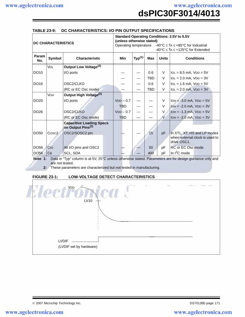
© 2007 Microchip Technology Inc. DS70138E-page 171
dsPIC30F3014/4013
FIGURE 23-1: LOW-VOLTAGE DETECT CHARACTERISTICS
TABLE 23-9: DC CHARACTERISTICS: I/O PIN OUTPUT SPECIFICATIONS
DC CHARACTERISTICS
Standard Operating Conditions: 2.5V to 5.5V(unless otherwise stated)Operating temperature -40°C ≤ TA ≤ +85°C for Industrial
-40°C ≤ TA ≤ +125°C for Extended
Param No.
Symbol Characteristic Min Typ(1) Max Units Conditions
VOL Output Low Voltage(2)
DO10 I/O ports — — 0.6 V IOL = 8.5 mA, VDD = 5V
— — TBD V IOL = 2.0 mA, VDD = 3V
DO16 OSC2/CLKO — — 0.6 V IOL = 1.6 mA, VDD = 5V
(RC or EC Osc mode) — — TBD V IOL = 2.0 mA, VDD = 3V
VOH Output High Voltage(2)
DO20 I/O ports VDD – 0.7 — — V IOH = -3.0 mA, VDD = 5V
TBD — — V IOH = -2.0 mA, VDD = 3V
DO26 OSC2/CLKO VDD – 0.7 — — V IOH = -1.3 mA, VDD = 5V
(RC or EC Osc mode) TBD — — V IOH = -2.0 mA, VDD = 3V
Capacitive Loading Specs on Output Pins(2)
DO50 COSC2 OSC2/SOSC2 pin — — 15 pF In XTL, XT, HS and LP modes when external clock is used to drive OSC1.
DO56 CIO All I/O pins and OSC2 — — 50 pF RC or EC Osc mode
DO58 CB SCL, SDA — — 400 pF In I2C mode
Note 1: Data in “Typ” column is at 5V, 25°C unless otherwise stated. Parameters are for design guidance only and are not tested.
2: These parameters are characterized but not tested in manufacturing.
LV10
LVDIF
VDD
(LVDIF set by hardware)
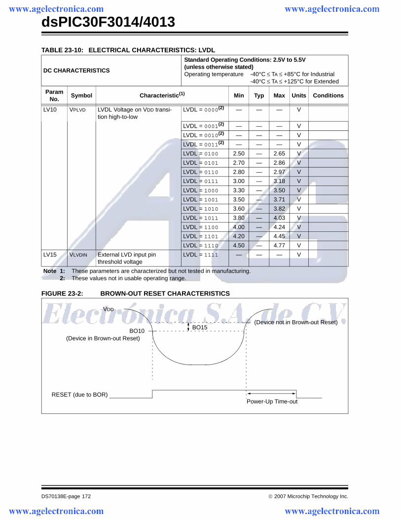
dsPIC30F3014/4013
DS70138E-page 172 © 2007 Microchip Technology Inc.
FIGURE 23-2: BROWN-OUT RESET CHARACTERISTICS
TABLE 23-10: ELECTRICAL CHARACTERISTICS: LVDL
DC CHARACTERISTICS
Standard Operating Conditions: 2.5V to 5.5V(unless otherwise stated)Operating temperature -40°C ≤ TA ≤ +85°C for Industrial
-40°C ≤ TA ≤ +125°C for Extended
ParamNo.
Symbol Characteristic(1) Min Typ Max Units Conditions
LV10 VPLVD LVDL Voltage on VDD transi-tion high-to-low
LVDL = 0000(2) — — — V
LVDL = 0001(2) — — — V
LVDL = 0010(2) — — — V
LVDL = 0011(2) — — — V
LVDL = 0100 2.50 — 2.65 V
LVDL = 0101 2.70 — 2.86 V
LVDL = 0110 2.80 — 2.97 V
LVDL = 0111 3.00 — 3.18 V
LVDL = 1000 3.30 — 3.50 V
LVDL = 1001 3.50 — 3.71 V
LVDL = 1010 3.60 — 3.82 V
LVDL = 1011 3.80 — 4.03 V
LVDL = 1100 4.00 — 4.24 V
LVDL = 1101 4.20 — 4.45 V
LVDL = 1110 4.50 — 4.77 V
LV15 VLVDIN External LVD input pinthreshold voltage
LVDL = 1111 — — — V
Note 1: These parameters are characterized but not tested in manufacturing.2: These values not in usable operating range.
BO10
RESET (due to BOR)
VDD
(Device in Brown-out Reset)
(Device not in Brown-out Reset)
Power-Up Time-out
BO15
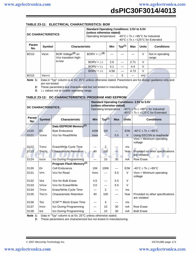
© 2007 Microchip Technology Inc. DS70138E-page 173
dsPIC30F3014/4013
TABLE 23-11: ELECTRICAL CHARACTERISTICS: BOR
DC CHARACTERISTICS
Standard Operating Conditions: 2.5V to 5.5V(unless otherwise stated)Operating temperature -40°C ≤ TA ≤ +85°C for Industrial
-40°C ≤ TA ≤ +125°C for Extended
ParamNo.
Symbol Characteristic Min Typ(1) Max Units Conditions
BO10 VBOR BOR Voltage(2) on VDD transition high-to-low
BORV = 11(3) — — — V Not in operating range
BORV = 10 2.6 — 2.71 V
BORV = 01 4.1 — 4.4 V
BORV = 00 4.58 — 4.73 V
BO15 VBHYS — 5 — mV
Note 1: Data in “Typ” column is at 5V, 25°C unless otherwise stated. Parameters are for design guidance only and are not tested.
2: These parameters are characterized but not tested in manufacturing.3: 11 values not in usable operating range.
TABLE 23-12: DC CHARACTERISTICS: PROGRAM AND EEPROM
DC CHARACTERISTICS
Standard Operating Conditions: 2.5V to 5.5V(unless otherwise stated)Operating temperature -40°C ≤ TA ≤ +85°C for Industrial
-40°C ≤ TA ≤ +125°C for Extended
ParamNo.
Symbol Characteristic Min Typ(1) Max Units Conditions
Data EEPROM Memory(2)
D120 ED Byte Endurance 100K 1M — E/W -40°C ≤ TA ≤ +85°C
D121 VDRW VDD for Read/Write VMIN — 5.5 V Using EECON to read/writeVMIN = Minimum operating voltage
D122 TDEW Erase/Write Cycle Time — 2 — ms
D123 TRETD Characteristic Retention 40 100 — Year Provided no other specifications are violated
D124 IDEW IDD During Programming — 10 30 mA Row Erase
Program Flash Memory(2)
D130 EP Cell Endurance 10K 100K — E/W -40°C ≤ TA ≤ +85°C
D131 VPR VDD for Read VMIN — 5.5 V VMIN = Minimum operating voltage
D132 VEB VDD for Bulk Erase 4.5 — 5.5 V
D133 VPEW VDD for Erase/Write 3.0 — 5.5 V
D134 TPEW Erase/Write Cycle Time — 2 — ms
D135 TRETD Characteristic Retention 40 100 — Year Provided no other specifications are violated
D136 TEB ICSP™ Block Erase Time — 4 — ms
D137 IPEW IDD During Programming — 10 30 mA Row Erase
D138 IEB IDD During Programming — 10 30 mA Bulk Erase
Note 1: Data in “Typ” column is at 5V, 25°C unless otherwise stated.2: These parameters are characterized but not tested in manufacturing.
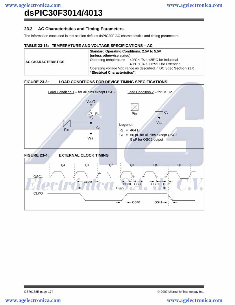
dsPIC30F3014/4013
DS70138E-page 174 © 2007 Microchip Technology Inc.
23.2 AC Characteristics and Timing Parameters
The information contained in this section defines dsPIC30F AC characteristics and timing parameters.
FIGURE 23-3: LOAD CONDITIONS FOR DEVICE TIMING SPECIFICATIONS
FIGURE 23-4: EXTERNAL CLOCK TIMING
TABLE 23-13: TEMPERATURE AND VOLTAGE SPECIFICATIONS – AC
AC CHARACTERISTICS
Standard Operating Conditions: 2.5V to 5.5V(unless otherwise stated)Operating temperature -40°C ≤ TA ≤ +85°C for Industrial
-40°C ≤ TA ≤ +125°C for ExtendedOperating voltage VDD range as described in DC Spec Section 23.0 “Electrical Characteristics”.
VDD/2
CL
RL
Pin
Pin
VSS
VSS
CL
RL = 464 ΩCL = 50 pF for all pins except OSC2
5 pF for OSC2 output
Load Condition 1 – for all pins except OSC2 Load Condition 2 – for OSC2
Legend:
OSC1
CLKO
Q4 Q1 Q2 Q3 Q4 Q1
OS20
OS25OS30 OS30
OS40 OS41
OS31 OS31
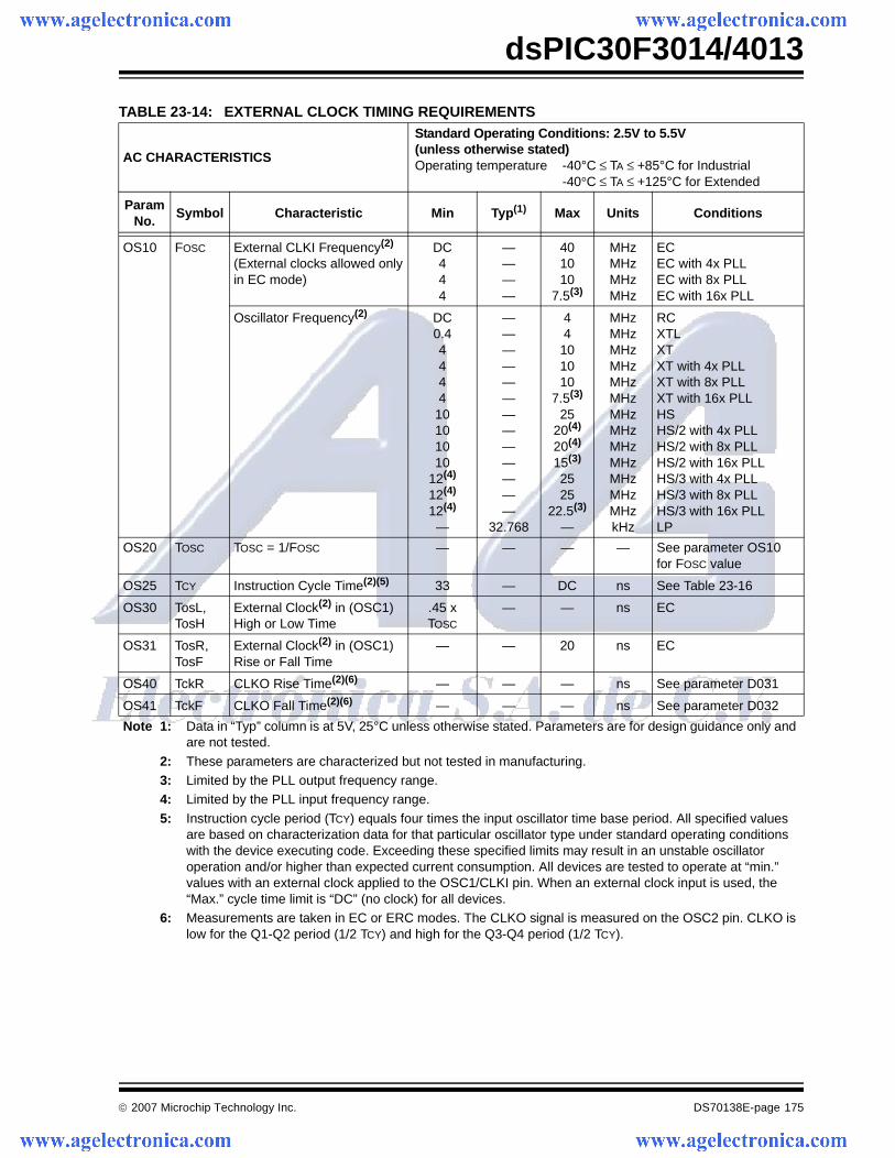
© 2007 Microchip Technology Inc. DS70138E-page 175
dsPIC30F3014/4013
TABLE 23-14: EXTERNAL CLOCK TIMING REQUIREMENTS
AC CHARACTERISTICS
Standard Operating Conditions: 2.5V to 5.5V(unless otherwise stated)Operating temperature -40°C ≤ TA ≤ +85°C for Industrial
-40°C ≤ TA ≤ +125°C for Extended
ParamNo.
Symbol Characteristic Min Typ(1) Max Units Conditions
OS10 FOSC External CLKI Frequency(2)
(External clocks allowed onlyin EC mode)
DC444
————
401010
7.5(3)
MHzMHzMHzMHz
ECEC with 4x PLLEC with 8x PLLEC with 16x PLL
Oscillator Frequency(2) DC0.44444
10101010
12(4)
12(4)
12(4)
—
—————————————
32.768
44
101010
7.5(3)
2520(4)
20(4)
15(3)
2525
22.5(3)
—
MHzMHzMHzMHzMHzMHzMHzMHzMHzMHzMHzMHzMHzkHz
RCXTLXTXT with 4x PLLXT with 8x PLLXT with 16x PLLHSHS/2 with 4x PLLHS/2 with 8x PLLHS/2 with 16x PLLHS/3 with 4x PLLHS/3 with 8x PLLHS/3 with 16x PLLLP
OS20 TOSC TOSC = 1/FOSC — — — — See parameter OS10for FOSC value
OS25 TCY Instruction Cycle Time(2)(5) 33 — DC ns See Table 23-16
OS30 TosL,TosH
External Clock(2) in (OSC1)High or Low Time
.45 x TOSC
— — ns EC
OS31 TosR,TosF
External Clock(2) in (OSC1)Rise or Fall Time
— — 20 ns EC
OS40 TckR CLKO Rise Time(2)(6) — — — ns See parameter D031
OS41 TckF CLKO Fall Time(2)(6) — — — ns See parameter D032
Note 1: Data in “Typ” column is at 5V, 25°C unless otherwise stated. Parameters are for design guidance only and are not tested.
2: These parameters are characterized but not tested in manufacturing.3: Limited by the PLL output frequency range.4: Limited by the PLL input frequency range.
5: Instruction cycle period (TCY) equals four times the input oscillator time base period. All specified values are based on characterization data for that particular oscillator type under standard operating conditions with the device executing code. Exceeding these specified limits may result in an unstable oscillator operation and/or higher than expected current consumption. All devices are tested to operate at “min.” values with an external clock applied to the OSC1/CLKI pin. When an external clock input is used, the “Max.” cycle time limit is “DC” (no clock) for all devices.
6: Measurements are taken in EC or ERC modes. The CLKO signal is measured on the OSC2 pin. CLKO is low for the Q1-Q2 period (1/2 TCY) and high for the Q3-Q4 period (1/2 TCY).
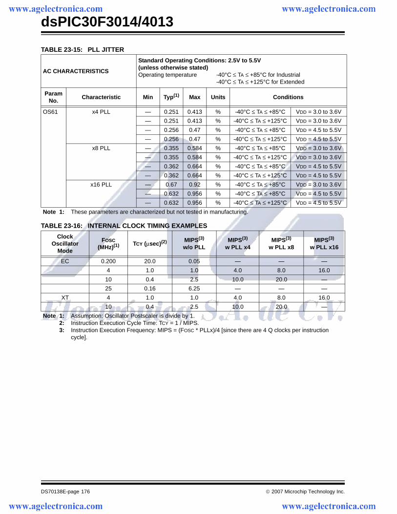
dsPIC30F3014/4013
DS70138E-page 176 © 2007 Microchip Technology Inc.
TABLE 23-15: PLL JITTER
AC CHARACTERISTICS
Standard Operating Conditions: 2.5V to 5.5V(unless otherwise stated)Operating temperature -40°C ≤ TA ≤ +85°C for Industrial
-40°C ≤ TA ≤ +125°C for Extended
Param No.
Characteristic Min Typ(1) Max Units Conditions
OS61 x4 PLL — 0.251 0.413 % -40°C ≤ TA ≤ +85°C VDD = 3.0 to 3.6V
— 0.251 0.413 % -40°C ≤ TA ≤ +125°C VDD = 3.0 to 3.6V
— 0.256 0.47 % -40°C ≤ TA ≤ +85°C VDD = 4.5 to 5.5V
— 0.256 0.47 % -40°C ≤ TA ≤ +125°C VDD = 4.5 to 5.5V
x8 PLL — 0.355 0.584 % -40°C ≤ TA ≤ +85°C VDD = 3.0 to 3.6V
— 0.355 0.584 % -40°C ≤ TA ≤ +125°C VDD = 3.0 to 3.6V
— 0.362 0.664 % -40°C ≤ TA ≤ +85°C VDD = 4.5 to 5.5V
— 0.362 0.664 % -40°C ≤ TA ≤ +125°C VDD = 4.5 to 5.5V
x16 PLL — 0.67 0.92 % -40°C ≤ TA ≤ +85°C VDD = 3.0 to 3.6V
— 0.632 0.956 % -40°C ≤ TA ≤ +85°C VDD = 4.5 to 5.5V
— 0.632 0.956 % -40°C ≤ TA ≤ +125°C VDD = 4.5 to 5.5V
Note 1: These parameters are characterized but not tested in manufacturing.
TABLE 23-16: INTERNAL CLOCK TIMING EXAMPLES
Clock Oscillator
Mode
FOSC (MHz)(1) TCY (μsec)(2) MIPS(3)
w/o PLLMIPS(3)
w PLL x4MIPS(3)
w PLL x8MIPS(3)
w PLL x16
EC 0.200 20.0 0.05 — — —
4 1.0 1.0 4.0 8.0 16.0
10 0.4 2.5 10.0 20.0 —
25 0.16 6.25 — — —
XT 4 1.0 1.0 4.0 8.0 16.0
10 0.4 2.5 10.0 20.0 —
Note 1: Assumption: Oscillator Postscaler is divide by 1.2: Instruction Execution Cycle Time: TCY = 1 / MIPS.3: Instruction Execution Frequency: MIPS = (FOSC * PLLx)/4 [since there are 4 Q clocks per instruction
cycle].
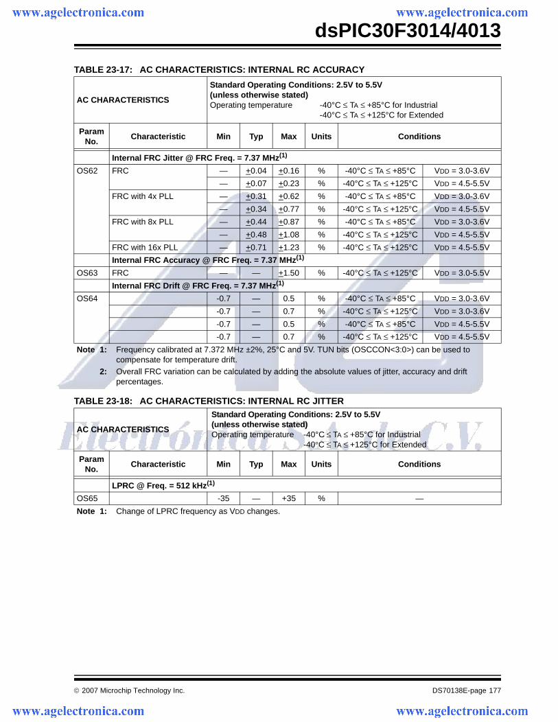
© 2007 Microchip Technology Inc. DS70138E-page 177
dsPIC30F3014/4013
TABLE 23-17: AC CHARACTERISTICS: INTERNAL RC ACCURACY
AC CHARACTERISTICS
Standard Operating Conditions: 2.5V to 5.5V(unless otherwise stated)Operating temperature -40°C ≤ TA ≤ +85°C for Industrial
-40°C ≤ TA ≤ +125°C for Extended
Param No.
Characteristic Min Typ Max Units Conditions
Internal FRC Jitter @ FRC Freq. = 7.37 MHz(1)
OS62 FRC — +0.04 +0.16 % -40°C ≤ TA ≤ +85°C VDD = 3.0-3.6V
— +0.07 +0.23 % -40°C ≤ TA ≤ +125°C VDD = 4.5-5.5V
FRC with 4x PLL — +0.31 +0.62 % -40°C ≤ TA ≤ +85°C VDD = 3.0-3.6V
— +0.34 +0.77 % -40°C ≤ TA ≤ +125°C VDD = 4.5-5.5V
FRC with 8x PLL — +0.44 +0.87 % -40°C ≤ TA ≤ +85°C VDD = 3.0-3.6V
— +0.48 +1.08 % -40°C ≤ TA ≤ +125°C VDD = 4.5-5.5V
FRC with 16x PLL — +0.71 +1.23 % -40°C ≤ TA ≤ +125°C VDD = 4.5-5.5V
Internal FRC Accuracy @ FRC Freq. = 7.37 MHz(1)
OS63 FRC — — +1.50 % -40°C ≤ TA ≤ +125°C VDD = 3.0-5.5V
Internal FRC Drift @ FRC Freq. = 7.37 MHz(1)
OS64 -0.7 — 0.5 % -40°C ≤ TA ≤ +85°C VDD = 3.0-3.6V
-0.7 — 0.7 % -40°C ≤ TA ≤ +125°C VDD = 3.0-3.6V
-0.7 — 0.5 % -40°C ≤ TA ≤ +85°C VDD = 4.5-5.5V
-0.7 — 0.7 % -40°C ≤ TA ≤ +125°C VDD = 4.5-5.5V
Note 1: Frequency calibrated at 7.372 MHz ±2%, 25°C and 5V. TUN bits (OSCCON<3:0>) can be used to compensate for temperature drift.
2: Overall FRC variation can be calculated by adding the absolute values of jitter, accuracy and drift percentages.
TABLE 23-18: AC CHARACTERISTICS: INTERNAL RC JITTER
AC CHARACTERISTICS
Standard Operating Conditions: 2.5V to 5.5V(unless otherwise stated)Operating temperature -40°C ≤ TA ≤ +85°C for Industrial
-40°C ≤ TA ≤ +125°C for Extended
ParamNo.
Characteristic Min Typ Max Units Conditions
LPRC @ Freq. = 512 kHz(1)
OS65 -35 — +35 % —
Note 1: Change of LPRC frequency as VDD changes.
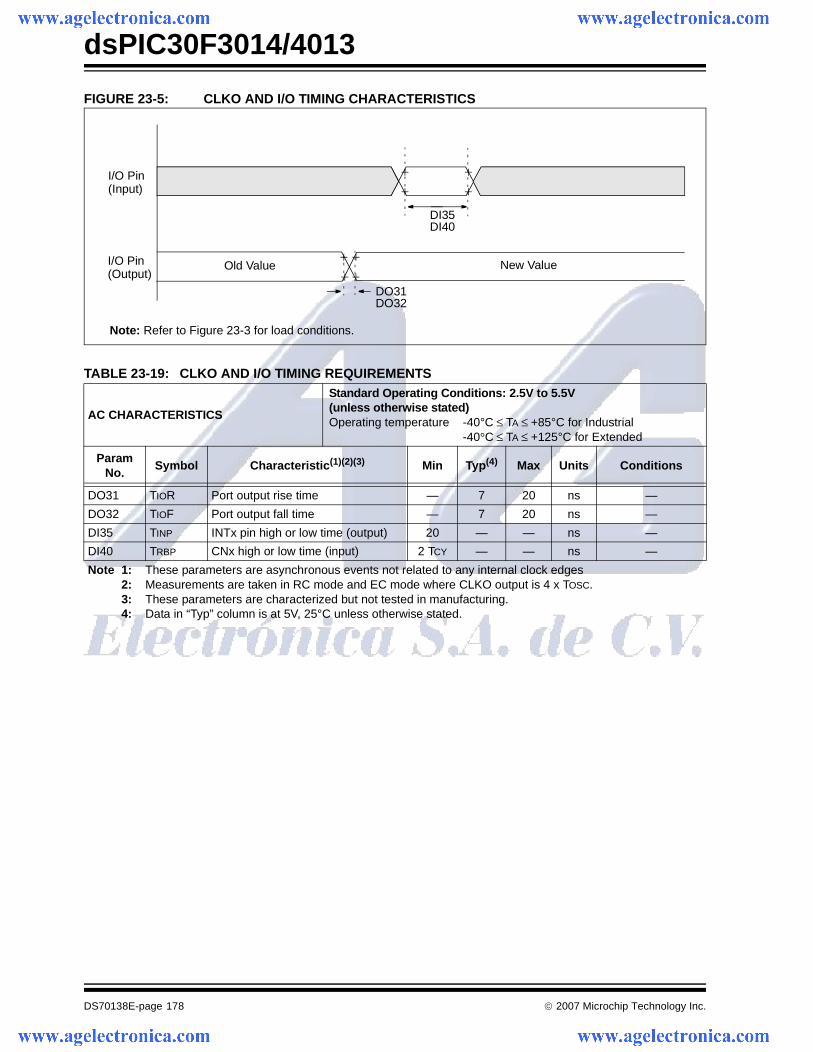
dsPIC30F3014/4013
DS70138E-page 178 © 2007 Microchip Technology Inc.
FIGURE 23-5: CLKO AND I/O TIMING CHARACTERISTICS
TABLE 23-19: CLKO AND I/O TIMING REQUIREMENTS
AC CHARACTERISTICS
Standard Operating Conditions: 2.5V to 5.5V(unless otherwise stated)Operating temperature -40°C ≤ TA ≤ +85°C for Industrial
-40°C ≤ TA ≤ +125°C for Extended
ParamNo.
Symbol Characteristic(1)(2)(3) Min Typ(4) Max Units Conditions
DO31 TIOR Port output rise time — 7 20 ns —
DO32 TIOF Port output fall time — 7 20 ns —
DI35 TINP INTx pin high or low time (output) 20 — — ns —
DI40 TRBP CNx high or low time (input) 2 TCY — — ns —
Note 1: These parameters are asynchronous events not related to any internal clock edges2: Measurements are taken in RC mode and EC mode where CLKO output is 4 x TOSC.3: These parameters are characterized but not tested in manufacturing.4: Data in “Typ” column is at 5V, 25°C unless otherwise stated.
Note: Refer to Figure 23-3 for load conditions.
I/O Pin(Input)
I/O Pin(Output)
DI35
Old Value New Value
DI40
DO31DO32
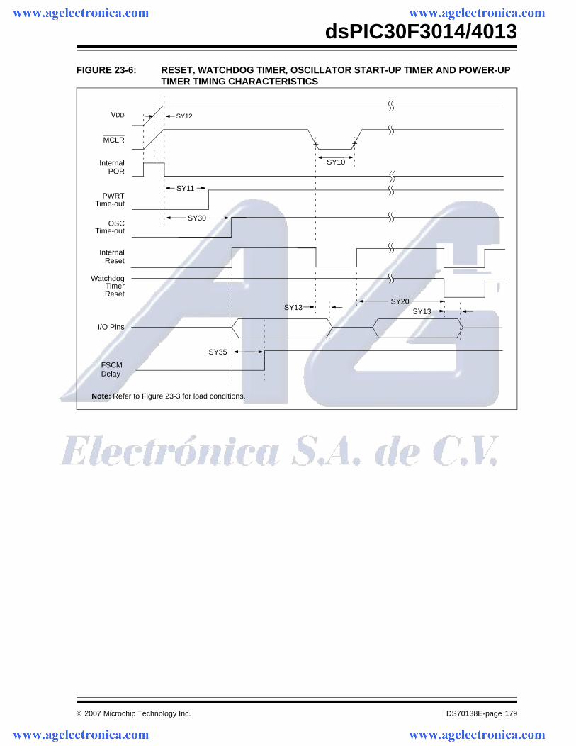
© 2007 Microchip Technology Inc. DS70138E-page 179
dsPIC30F3014/4013
FIGURE 23-6: RESET, WATCHDOG TIMER, OSCILLATOR START-UP TIMER AND POWER-UP TIMER TIMING CHARACTERISTICS
VDD
MCLR
InternalPOR
PWRTTime-out
OSCTime-out
InternalReset
WatchdogTimerReset
SY11
SY10
SY20SY13
I/O Pins
SY13
Note: Refer to Figure 23-3 for load conditions.
FSCMDelay
SY35
SY30
SY12
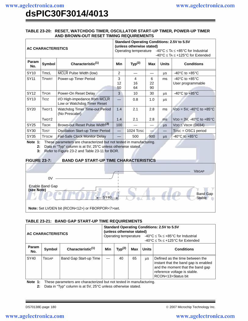
dsPIC30F3014/4013
DS70138E-page 180 © 2007 Microchip Technology Inc.
FIGURE 23-7: BAND GAP START-UP TIME CHARACTERISTICS
TABLE 23-20: RESET, WATCHDOG TIMER, OSCILLATOR START-UP TIMER, POWER-UP TIMER AND BROWN-OUT RESET TIMING REQUIREMENTS
AC CHARACTERISTICS
Standard Operating Conditions: 2.5V to 5.5V(unless otherwise stated)Operating temperature -40°C ≤ TA ≤ +85°C for Industrial
-40°C ≤ TA ≤ +125°C for Extended
ParamNo.
Symbol Characteristic(1) Min Typ(2) Max Units Conditions
SY10 TmcL MCLR Pulse Width (low) 2 — — μs -40°C to +85°C
SY11 TPWRT Power-up Timer Period 31250
41664
62290
ms -40°C to +85°CUser programmable
SY12 TPOR Power-On Reset Delay 3 10 30 μs -40°C to +85°C
SY13 TIOZ I/O High-impedance from MCLR Low or Watchdog Timer Reset
— 0.8 1.0 μs
SY20 TWDT1 Watchdog Timer Time-out Period (No Prescaler)
1.4 2.1 2.8 ms VDD = 5V, -40°C to +85°C
TWDT2 1.4 2.1 2.8 ms VDD = 3V, -40°C to +85°C
SY25 TBOR Brown-out Reset Pulse Width(3) 100 — — μs VDD ≤ VBOR (D034)
SY30 TOST Oscillation Start-up Timer Period — 1024 TOSC — — TOSC = OSC1 period
SY35 TFSCM Fail-Safe Clock Monitor Delay — 500 900 μs -40°C to +85°C
Note 1: These parameters are characterized but not tested in manufacturing.2: Data in “Typ” column is at 5V, 25°C unless otherwise stated.3: Refer to Figure 23-2 and Table 23-11 for BOR.
TABLE 23-21: BAND GAP START-UP TIME REQUIREMENTS
AC CHARACTERISTICS
Standard Operating Conditions: 2.5V to 5.5V(unless otherwise stated)Operating temperature -40°C ≤ TA ≤ +85°C for Industrial
-40°C ≤ TA ≤ +125°C for Extended
ParamNo.
Symbol Characteristic(1) Min Typ(2) Max Units Conditions
SY40 TBGAP Band Gap Start-up Time — 40 65 μs Defined as the time between the instant that the band gap is enabled and the moment that the band gap reference voltage is stable. RCON<13>Status bit
Note 1: These parameters are characterized but not tested in manufacturing.2: Data in “Typ” column is at 5V, 25°C unless otherwise stated.
VBGAP
Enable Band Gap
Band Gap
0V
(see Note)
Stable
Note: Set LVDEN bit (RCON<12>) or FBORPOR<7>set.
SY40
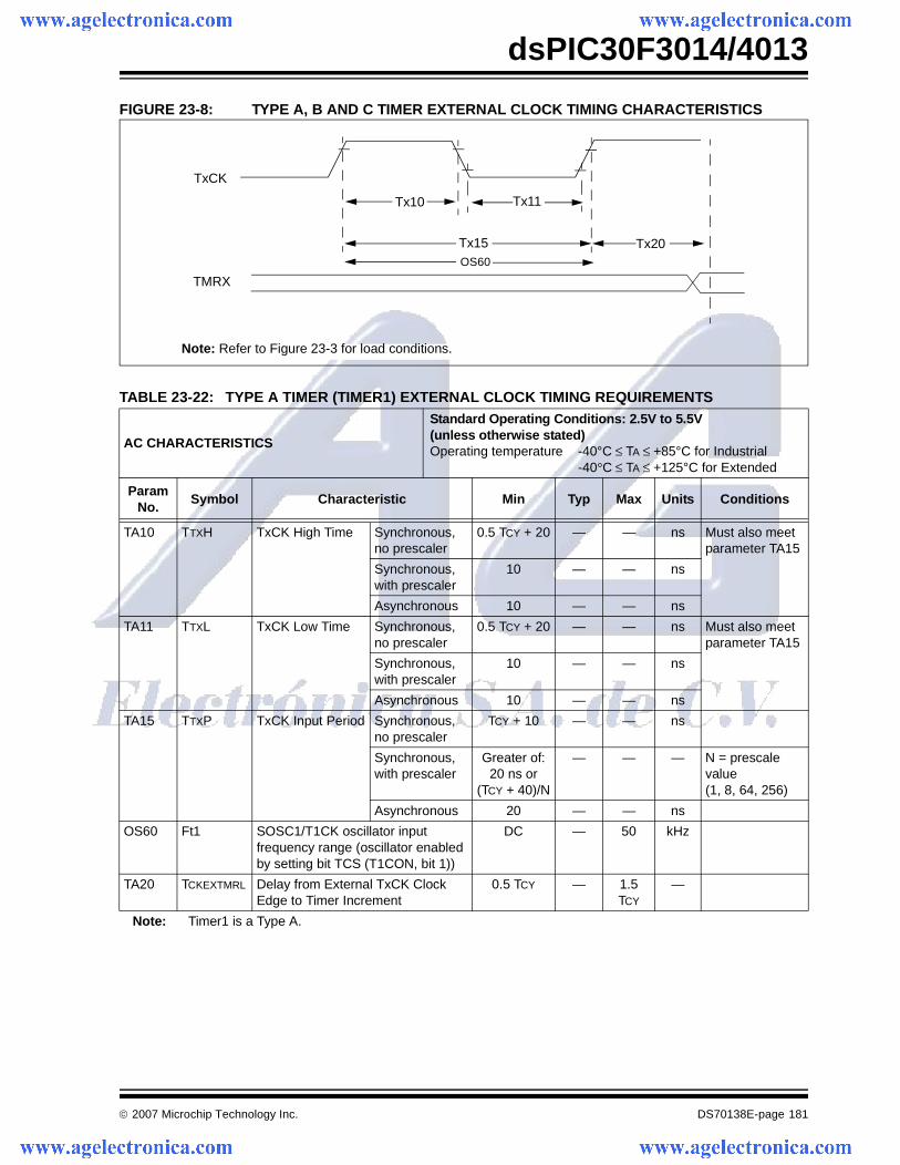
© 2007 Microchip Technology Inc. DS70138E-page 181
dsPIC30F3014/4013
FIGURE 23-8: TYPE A, B AND C TIMER EXTERNAL CLOCK TIMING CHARACTERISTICS
TABLE 23-22: TYPE A TIMER (TIMER1) EXTERNAL CLOCK TIMING REQUIREMENTS
AC CHARACTERISTICS
Standard Operating Conditions: 2.5V to 5.5V(unless otherwise stated)Operating temperature -40°C ≤ TA ≤ +85°C for Industrial
-40°C ≤ TA ≤ +125°C for Extended
ParamNo.
Symbol Characteristic Min Typ Max Units Conditions
TA10 TTXH TxCK High Time Synchronous,no prescaler
0.5 TCY + 20 — — ns Must also meet parameter TA15
Synchronous,with prescaler
10 — — ns
Asynchronous 10 — — ns
TA11 TTXL TxCK Low Time Synchronous,no prescaler
0.5 TCY + 20 — — ns Must also meet parameter TA15
Synchronous,with prescaler
10 — — ns
Asynchronous 10 — — ns
TA15 TTXP TxCK Input Period Synchronous,no prescaler
TCY + 10 — — ns
Synchronous,with prescaler
Greater of:20 ns or
(TCY + 40)/N
— — — N = prescale value(1, 8, 64, 256)
Asynchronous 20 — — ns
OS60 Ft1 SOSC1/T1CK oscillator input frequency range (oscillator enabled by setting bit TCS (T1CON, bit 1))
DC — 50 kHz
TA20 TCKEXTMRL Delay from External TxCK Clock Edge to Timer Increment
0.5 TCY — 1.5 TCY
—
Note: Timer1 is a Type A.
Note: Refer to Figure 23-3 for load conditions.
Tx11
Tx15
Tx10
Tx20
TMRX
OS60
TxCK
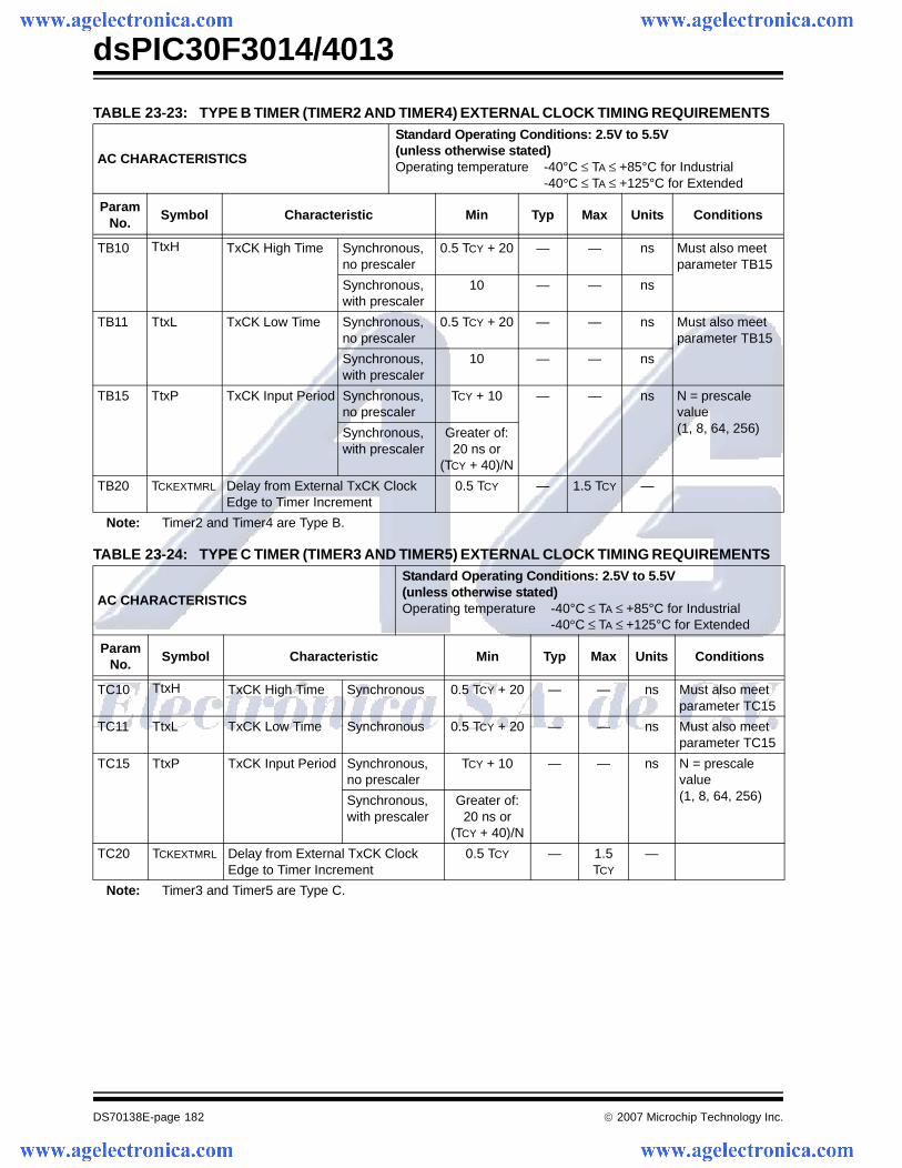
dsPIC30F3014/4013
DS70138E-page 182 © 2007 Microchip Technology Inc.
TABLE 23-23: TYPE B TIMER (TIMER2 AND TIMER4) EXTERNAL CLOCK TIMING REQUIREMENTS
AC CHARACTERISTICS
Standard Operating Conditions: 2.5V to 5.5V(unless otherwise stated)Operating temperature -40°C ≤ TA ≤ +85°C for Industrial
-40°C ≤ TA ≤ +125°C for Extended
ParamNo.
Symbol Characteristic Min Typ Max Units Conditions
TB10 TtxH TxCK High Time Synchronous,no prescaler
0.5 TCY + 20 — — ns Must also meet parameter TB15
Synchronous,with prescaler
10 — — ns
TB11 TtxL TxCK Low Time Synchronous,no prescaler
0.5 TCY + 20 — — ns Must also meet parameter TB15
Synchronous,with prescaler
10 — — ns
TB15 TtxP TxCK Input Period Synchronous,no prescaler
TCY + 10 — — ns N = prescale value(1, 8, 64, 256)Synchronous,
with prescalerGreater of:
20 ns or(TCY + 40)/N
TB20 TCKEXTMRL Delay from External TxCK Clock Edge to Timer Increment
0.5 TCY — 1.5 TCY —
Note: Timer2 and Timer4 are Type B.
TABLE 23-24: TYPE C TIMER (TIMER3 AND TIMER5) EXTERNAL CLOCK TIMING REQUIREMENTS
AC CHARACTERISTICS
Standard Operating Conditions: 2.5V to 5.5V(unless otherwise stated)Operating temperature -40°C ≤ TA ≤ +85°C for Industrial
-40°C ≤ TA ≤ +125°C for Extended
ParamNo.
Symbol Characteristic Min Typ Max Units Conditions
TC10 TtxH TxCK High Time Synchronous 0.5 TCY + 20 — — ns Must also meet parameter TC15
TC11 TtxL TxCK Low Time Synchronous 0.5 TCY + 20 — — ns Must also meet parameter TC15
TC15 TtxP TxCK Input Period Synchronous,no prescaler
TCY + 10 — — ns N = prescalevalue (1, 8, 64, 256)Synchronous,
with prescalerGreater of:
20 ns or (TCY + 40)/N
TC20 TCKEXTMRL Delay from External TxCK Clock Edge to Timer Increment
0.5 TCY — 1.5 TCY
—
Note: Timer3 and Timer5 are Type C.
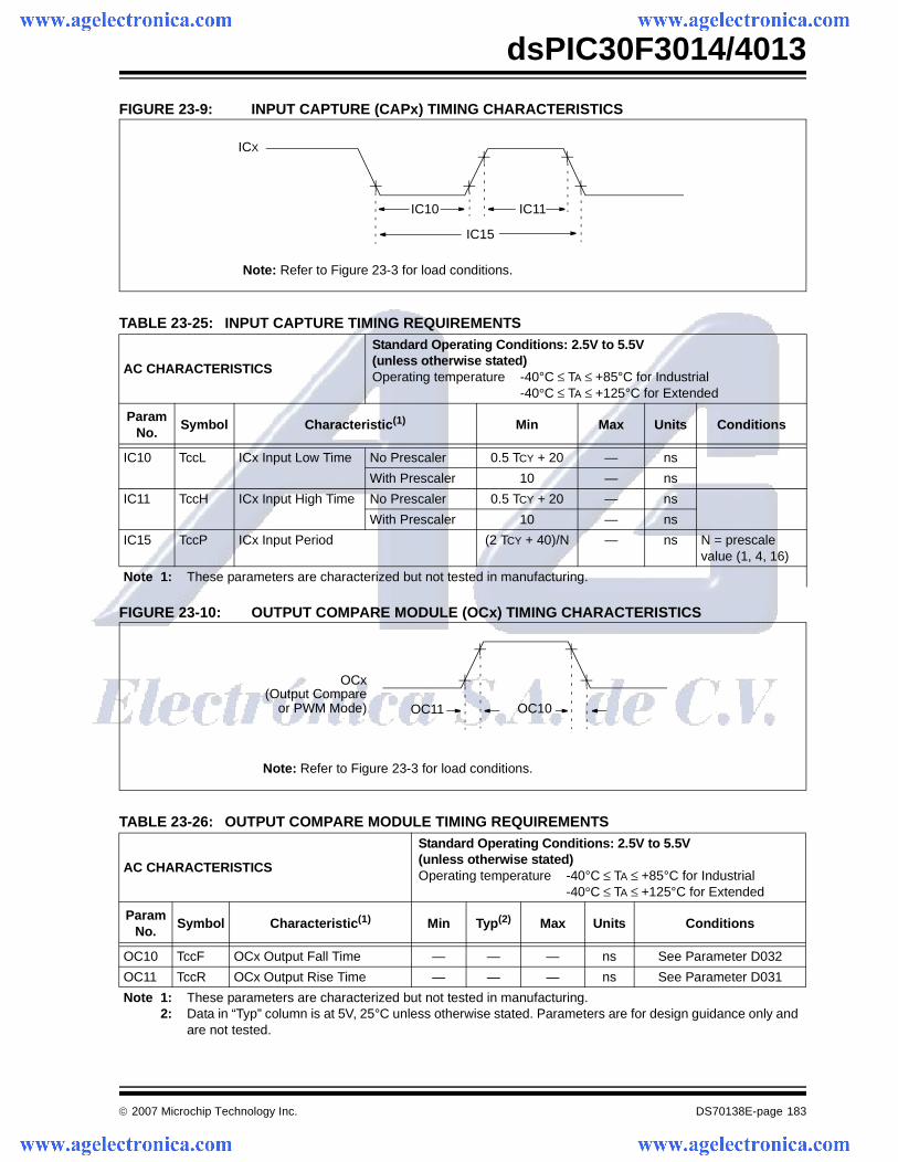
© 2007 Microchip Technology Inc. DS70138E-page 183
dsPIC30F3014/4013
FIGURE 23-9: INPUT CAPTURE (CAPx) TIMING CHARACTERISTICS
FIGURE 23-10: OUTPUT COMPARE MODULE (OCx) TIMING CHARACTERISTICS
TABLE 23-25: INPUT CAPTURE TIMING REQUIREMENTS
AC CHARACTERISTICS
Standard Operating Conditions: 2.5V to 5.5V(unless otherwise stated)Operating temperature -40°C ≤ TA ≤ +85°C for Industrial
-40°C ≤ TA ≤ +125°C for Extended
ParamNo.
Symbol Characteristic(1) Min Max Units Conditions
IC10 TccL ICx Input Low Time No Prescaler 0.5 TCY + 20 — ns
With Prescaler 10 — ns
IC11 TccH ICx Input High Time No Prescaler 0.5 TCY + 20 — ns
With Prescaler 10 — ns
IC15 TccP ICx Input Period (2 TCY + 40)/N — ns N = prescale value (1, 4, 16)
Note 1: These parameters are characterized but not tested in manufacturing.
TABLE 23-26: OUTPUT COMPARE MODULE TIMING REQUIREMENTS
AC CHARACTERISTICS
Standard Operating Conditions: 2.5V to 5.5V(unless otherwise stated)Operating temperature -40°C ≤ TA ≤ +85°C for Industrial
-40°C ≤ TA ≤ +125°C for Extended
Param No.
Symbol Characteristic(1) Min Typ(2) Max Units Conditions
OC10 TccF OCx Output Fall Time — — — ns See Parameter D032
OC11 TccR OCx Output Rise Time — — — ns See Parameter D031
Note 1: These parameters are characterized but not tested in manufacturing.2: Data in “Typ” column is at 5V, 25°C unless otherwise stated. Parameters are for design guidance only and
are not tested.
ICX
IC10 IC11
IC15
Note: Refer to Figure 23-3 for load conditions.
OCx
OC11 OC10(Output Compare
Note: Refer to Figure 23-3 for load conditions.
or PWM Mode)
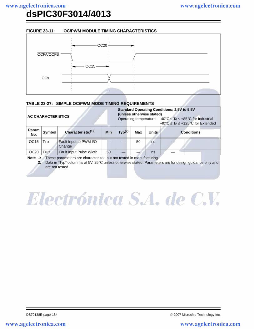
dsPIC30F3014/4013
DS70138E-page 184 © 2007 Microchip Technology Inc.
FIGURE 23-11: OC/PWM MODULE TIMING CHARACTERISTICS
TABLE 23-27: SIMPLE OC/PWM MODE TIMING REQUIREMENTS
AC CHARACTERISTICS
Standard Operating Conditions: 2.5V to 5.5V(unless otherwise stated)Operating temperature -40°C ≤ TA ≤ +85°C for Industrial
-40°C ≤ TA ≤ +125°C for Extended
Param No.
Symbol Characteristic(1) Min Typ(2) Max Units Conditions
OC15 TFD Fault Input to PWM I/O Change
— — 50 ns —
OC20 TFLT Fault Input Pulse Width 50 — — ns —
Note 1: These parameters are characterized but not tested in manufacturing.2: Data in “Typ” column is at 5V, 25°C unless otherwise stated. Parameters are for design guidance only and
are not tested.
OCFA/OCFB
OCx
OC20
OC15
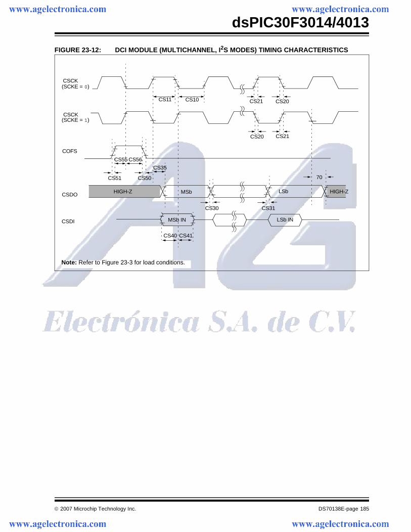
© 2007 Microchip Technology Inc. DS70138E-page 185
dsPIC30F3014/4013
FIGURE 23-12: DCI MODULE (MULTICHANNEL, I2S MODES) TIMING CHARACTERISTICS
COFS
CSCK(SCKE = 0)
CSCK(SCKE = 1)
CSDO
CSDI
CS11 CS10
CS40 CS41
CS21CS20
CS35
CS21
MSb LSb
MSb IN LSb IN
CS31
HIGH-Z HIGH-Z
70
CS30
CS51 CS50
CS55
Note: Refer to Figure 23-3 for load conditions.
CS20
CS56
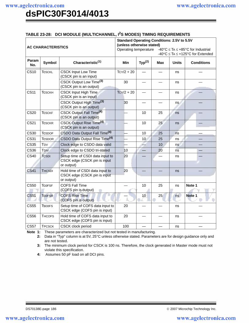
dsPIC30F3014/4013
DS70138E-page 186 © 2007 Microchip Technology Inc.
TABLE 23-28: DCI MODULE (MULTICHANNEL, I2S MODES) TIMING REQUIREMENTS
AC CHARACTERISTICS
Standard Operating Conditions: 2.5V to 5.5V(unless otherwise stated)Operating temperature -40°C ≤ TA ≤ +85°C for Industrial
-40°C ≤ TA ≤ +125°C for Extended
ParamNo.
Symbol Characteristic(1) Min Typ(2) Max Units Conditions
CS10 TcSCKL CSCK Input Low Time(CSCK pin is an input)
TCY/2 + 20 — — ns —
CSCK Output Low Time(3)
(CSCK pin is an output)30 — — ns —
CS11 TcSCKH CSCK Input High Time(CSCK pin is an input)
TCY/2 + 20 — — ns —
CSCK Output High Time(3)
(CSCK pin is an output)30 — — ns —
CS20 TcSCKF CSCK Output Fall Time(4)
(CSCK pin is an output)— 10 25 ns —
CS21 TcSCKR CSCK Output Rise Time(4)
(CSCK pin is an output)— 10 25 ns —
CS30 TcSDOF CSDO Data Output Fall Time(4) — 10 25 ns —
CS31 TcSDOR CSDO Data Output Rise Time(4) — 10 25 ns —
CS35 TDV Clock edge to CSDO data valid — — 10 ns —
CS36 TDIV Clock edge to CSDO tri-stated 10 — 20 ns —
CS40 TCSDI Setup time of CSDI data input toCSCK edge (CSCK pin is inputor output)
20 — — ns —
CS41 THCSDI Hold time of CSDI data input toCSCK edge (CSCK pin is inputor output)
20 — — ns —
CS50 TcoFSF COFS Fall Time(COFS pin is output)
— 10 25 ns Note 1
CS51 TcoFSR COFS Rise Time(COFS pin is output)
— 10 25 ns Note 1
CS55 TscoFS Setup time of COFS data input toCSCK edge (COFS pin is input)
20 — — ns —
CS56 THCOFS Hold time of COFS data input toCSCK edge (COFS pin is input)
20 — — ns —
CS57 TPCSCK CSCK clock period 100 — — ns —
Note 1: These parameters are characterized but not tested in manufacturing.2: Data in “Typ” column is at 5V, 25°C unless otherwise stated. Parameters are for design guidance only and
are not tested.3: The minimum clock period for CSCK is 100 ns. Therefore, the clock generated in Master mode must not
violate this specification.4: Assumes 50 pF load on all DCI pins.
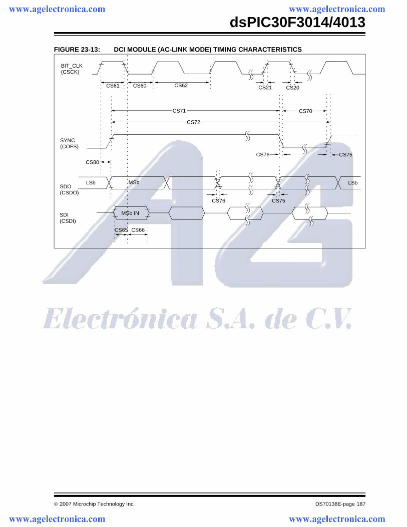
© 2007 Microchip Technology Inc. DS70138E-page 187
dsPIC30F3014/4013
FIGURE 23-13: DCI MODULE (AC-LINK MODE) TIMING CHARACTERISTICS
SYNC
BIT_CLK
SDO
SDI
CS61 CS60
CS65 CS66
CS80
CS21
MSb IN
CS75
LSb
CS76
(COFS)
(CSCK)
LSbMSb
CS72
CS71 CS70
CS76 CS75
(CSDO)
(CSDI)
CS62 CS20
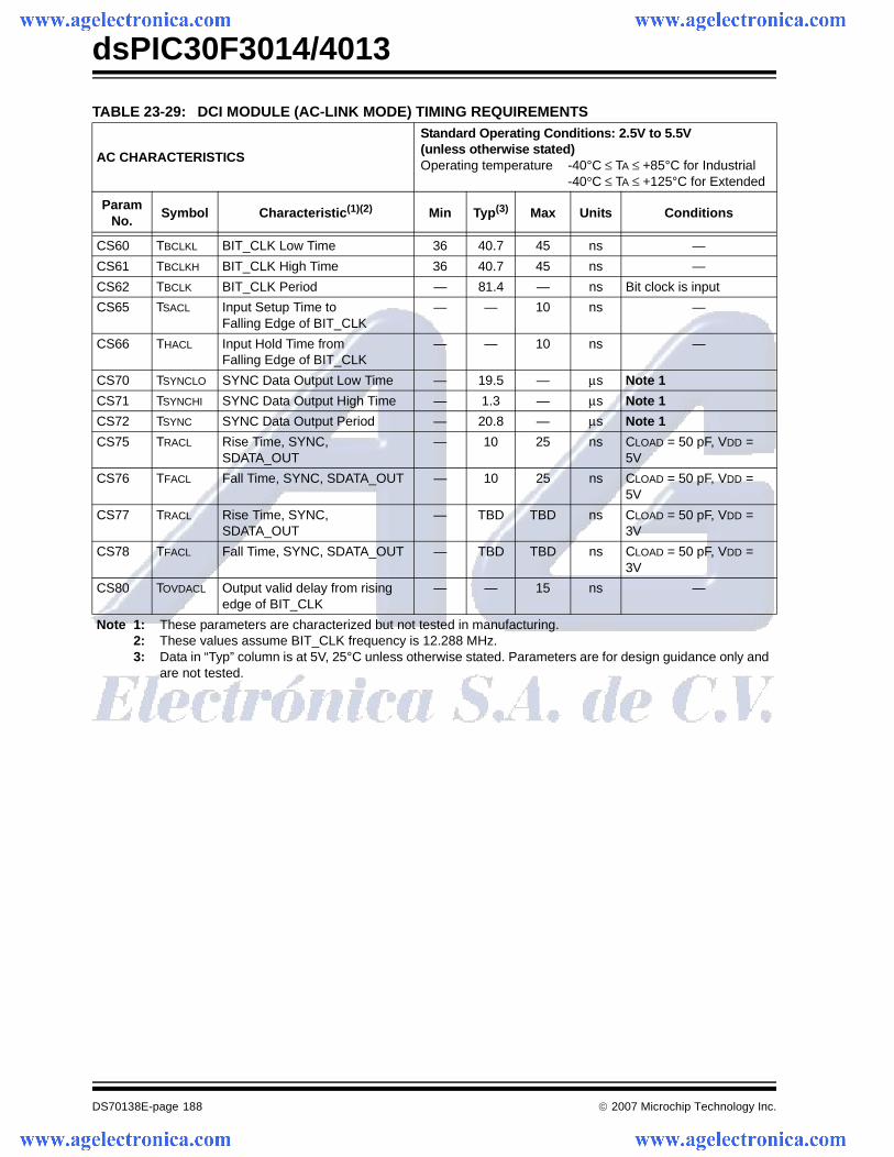
dsPIC30F3014/4013
DS70138E-page 188 © 2007 Microchip Technology Inc.
TABLE 23-29: DCI MODULE (AC-LINK MODE) TIMING REQUIREMENTS
AC CHARACTERISTICS
Standard Operating Conditions: 2.5V to 5.5V(unless otherwise stated)Operating temperature -40°C ≤ TA ≤ +85°C for Industrial
-40°C ≤ TA ≤ +125°C for Extended
ParamNo.
Symbol Characteristic(1)(2) Min Typ(3) Max Units Conditions
CS60 TBCLKL BIT_CLK Low Time 36 40.7 45 ns —
CS61 TBCLKH BIT_CLK High Time 36 40.7 45 ns —
CS62 TBCLK BIT_CLK Period — 81.4 — ns Bit clock is input
CS65 TSACL Input Setup Time toFalling Edge of BIT_CLK
— — 10 ns —
CS66 THACL Input Hold Time fromFalling Edge of BIT_CLK
— — 10 ns —
CS70 TSYNCLO SYNC Data Output Low Time — 19.5 — μs Note 1
CS71 TSYNCHI SYNC Data Output High Time — 1.3 — μs Note 1
CS72 TSYNC SYNC Data Output Period — 20.8 — μs Note 1
CS75 TRACL Rise Time, SYNC, SDATA_OUT
— 10 25 ns CLOAD = 50 pF, VDD = 5V
CS76 TFACL Fall Time, SYNC, SDATA_OUT — 10 25 ns CLOAD = 50 pF, VDD = 5V
CS77 TRACL Rise Time, SYNC, SDATA_OUT
— TBD TBD ns CLOAD = 50 pF, VDD = 3V
CS78 TFACL Fall Time, SYNC, SDATA_OUT — TBD TBD ns CLOAD = 50 pF, VDD = 3V
CS80 TOVDACL Output valid delay from rising edge of BIT_CLK
— — 15 ns —
Note 1: These parameters are characterized but not tested in manufacturing.2: These values assume BIT_CLK frequency is 12.288 MHz.3: Data in “Typ” column is at 5V, 25°C unless otherwise stated. Parameters are for design guidance only and
are not tested.
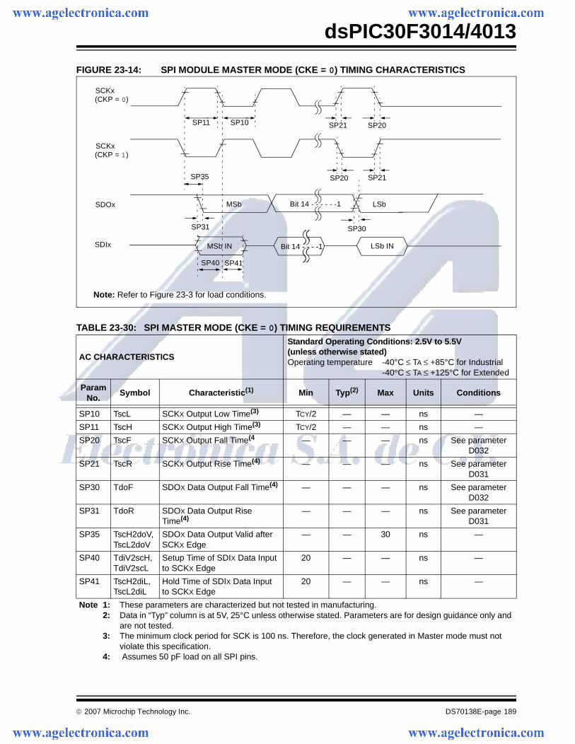
© 2007 Microchip Technology Inc. DS70138E-page 189
dsPIC30F3014/4013
FIGURE 23-14: SPI MODULE MASTER MODE (CKE = 0) TIMING CHARACTERISTICS
TABLE 23-30: SPI MASTER MODE (CKE = 0) TIMING REQUIREMENTS
AC CHARACTERISTICS
Standard Operating Conditions: 2.5V to 5.5V(unless otherwise stated)Operating temperature -40°C ≤ TA ≤ +85°C for Industrial
-40°C ≤ TA ≤ +125°C for Extended
ParamNo.
Symbol Characteristic(1) Min Typ(2) Max Units Conditions
SP10 TscL SCKX Output Low Time(3) TCY/2 — — ns —
SP11 TscH SCKX Output High Time(3) TCY/2 — — ns —
SP20 TscF SCKX Output Fall Time(4 — — — ns See parameter D032
SP21 TscR SCKX Output Rise Time(4) — — — ns See parameter D031
SP30 TdoF SDOX Data Output Fall Time(4) — — — ns See parameter D032
SP31 TdoR SDOX Data Output Rise Time(4)
— — — ns See parameter D031
SP35 TscH2doV,TscL2doV
SDOX Data Output Valid after SCKX Edge
— — 30 ns —
SP40 TdiV2scH,TdiV2scL
Setup Time of SDIX Data Inputto SCKX Edge
20 — — ns —
SP41 TscH2diL,TscL2diL
Hold Time of SDIX Data Inputto SCKX Edge
20 — — ns —
Note 1: These parameters are characterized but not tested in manufacturing.2: Data in “Typ” column is at 5V, 25°C unless otherwise stated. Parameters are for design guidance only and
are not tested.3: The minimum clock period for SCK is 100 ns. Therefore, the clock generated in Master mode must not
violate this specification.4: Assumes 50 pF load on all SPI pins.
SCKx(CKP = 0)
SCKx(CKP = 1)
SDOx
SDIx
SP11 SP10
SP40 SP41
SP21SP20SP35
SP20SP21
MSb LSbBit 14 - - - - - -1
MSb IN LSb INBit 14 - - - -1
SP30SP31
Note: Refer to Figure 23-3 for load conditions.
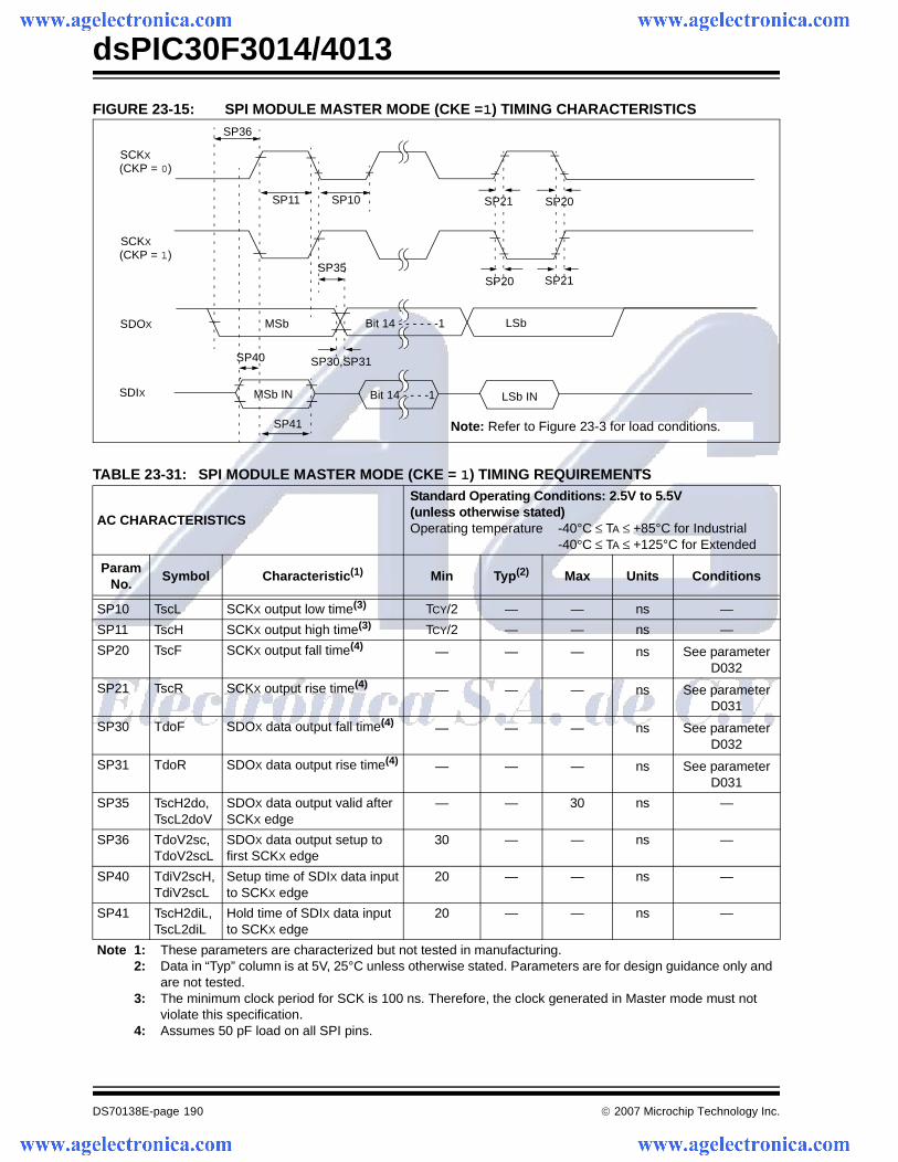
dsPIC30F3014/4013
DS70138E-page 190 © 2007 Microchip Technology Inc.
FIGURE 23-15: SPI MODULE MASTER MODE (CKE =1) TIMING CHARACTERISTICS
TABLE 23-31: SPI MODULE MASTER MODE (CKE = 1) TIMING REQUIREMENTS
AC CHARACTERISTICS
Standard Operating Conditions: 2.5V to 5.5V(unless otherwise stated)Operating temperature -40°C ≤ TA ≤ +85°C for Industrial
-40°C ≤ TA ≤ +125°C for Extended
ParamNo.
Symbol Characteristic(1) Min Typ(2) Max Units Conditions
SP10 TscL SCKX output low time(3) TCY/2 — — ns —
SP11 TscH SCKX output high time(3) TCY/2 — — ns —
SP20 TscF SCKX output fall time(4) — — — ns See parameter D032
SP21 TscR SCKX output rise time(4) — — — ns See parameter D031
SP30 TdoF SDOX data output fall time(4) — — — ns See parameter D032
SP31 TdoR SDOX data output rise time(4) — — — ns See parameter D031
SP35 TscH2do,TscL2doV
SDOX data output valid afterSCKX edge
— — 30 ns —
SP36 TdoV2sc, TdoV2scL
SDOX data output setup tofirst SCKX edge
30 — — ns —
SP40 TdiV2scH, TdiV2scL
Setup time of SDIX data inputto SCKX edge
20 — — ns —
SP41 TscH2diL, TscL2diL
Hold time of SDIX data inputto SCKX edge
20 — — ns —
Note 1: These parameters are characterized but not tested in manufacturing.2: Data in “Typ” column is at 5V, 25°C unless otherwise stated. Parameters are for design guidance only and
are not tested.3: The minimum clock period for SCK is 100 ns. Therefore, the clock generated in Master mode must not
violate this specification.4: Assumes 50 pF load on all SPI pins.
SCKX
(CKP = 0)
SCKX
(CKP = 1)
SDOX
SDIX
SP36
SP30,SP31
SP35
MSb
MSb IN
Bit 14 - - - - - -1
LSb INBit 14 - - - -1
LSb
Note: Refer to Figure 23-3 for load conditions.
SP11 SP10 SP20SP21
SP21SP20
SP40
SP41
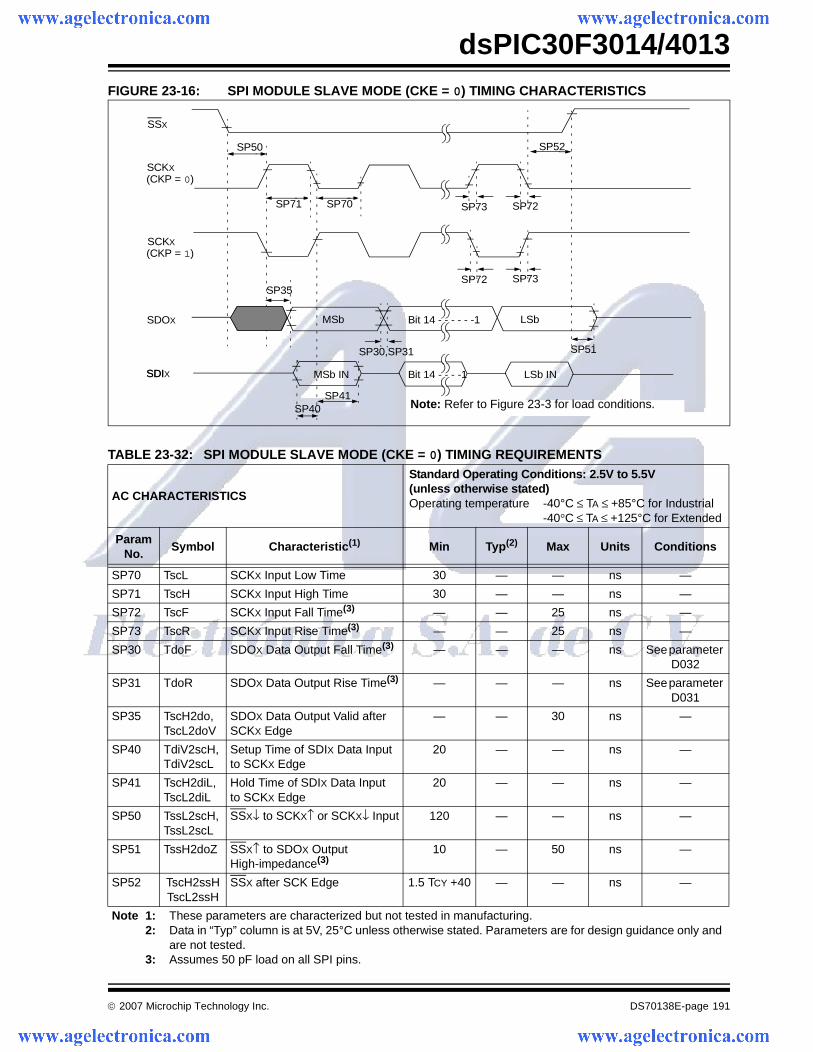
© 2007 Microchip Technology Inc. DS70138E-page 191
dsPIC30F3014/4013FIGURE 23-16: SPI MODULE SLAVE MODE (CKE = 0) TIMING CHARACTERISTICS
TABLE 23-32: SPI MODULE SLAVE MODE (CKE = 0) TIMING REQUIREMENTS
AC CHARACTERISTICS
Standard Operating Conditions: 2.5V to 5.5V(unless otherwise stated)Operating temperature -40°C ≤ TA ≤ +85°C for Industrial
-40°C ≤ TA ≤ +125°C for Extended
ParamNo.
Symbol Characteristic(1) Min Typ(2) Max Units Conditions
SP70 TscL SCKX Input Low Time 30 — — ns —
SP71 TscH SCKX Input High Time 30 — — ns —
SP72 TscF SCKX Input Fall Time(3) — — 25 ns —
SP73 TscR SCKX Input Rise Time(3) — — 25 ns —
SP30 TdoF SDOX Data Output Fall Time(3) — — — ns See parameter D032
SP31 TdoR SDOX Data Output Rise Time(3) — — — ns See parameter D031
SP35 TscH2do,TscL2doV
SDOX Data Output Valid afterSCKX Edge
— — 30 ns —
SP40 TdiV2scH, TdiV2scL
Setup Time of SDIX Data Inputto SCKX Edge
20 — — ns —
SP41 TscH2diL, TscL2diL
Hold Time of SDIX Data Inputto SCKX Edge
20 — — ns —
SP50 TssL2scH, TssL2scL
SSX↓ to SCKX↑ or SCKX↓ Input 120 — — ns —
SP51 TssH2doZ SSX↑ to SDOX OutputHigh-impedance(3)
10 — 50 ns —
SP52 TscH2ssHTscL2ssH
SSX after SCK Edge 1.5 TCY +40 — — ns —
Note 1: These parameters are characterized but not tested in manufacturing.2: Data in “Typ” column is at 5V, 25°C unless otherwise stated. Parameters are for design guidance only and
are not tested.3: Assumes 50 pF load on all SPI pins.
SSX
SCKX(CKP = 0)
SCKX(CKP = 1)
SDOX
SDI
SP50
SP40SP41
SP30,SP31 SP51
SP35
SDIX
MSb LSbBit 14 - - - - - -1
MSb IN Bit 14 - - - -1 LSb IN
SP52
SP73SP72
SP72SP73SP71 SP70
Note: Refer to Figure 23-3 for load conditions.
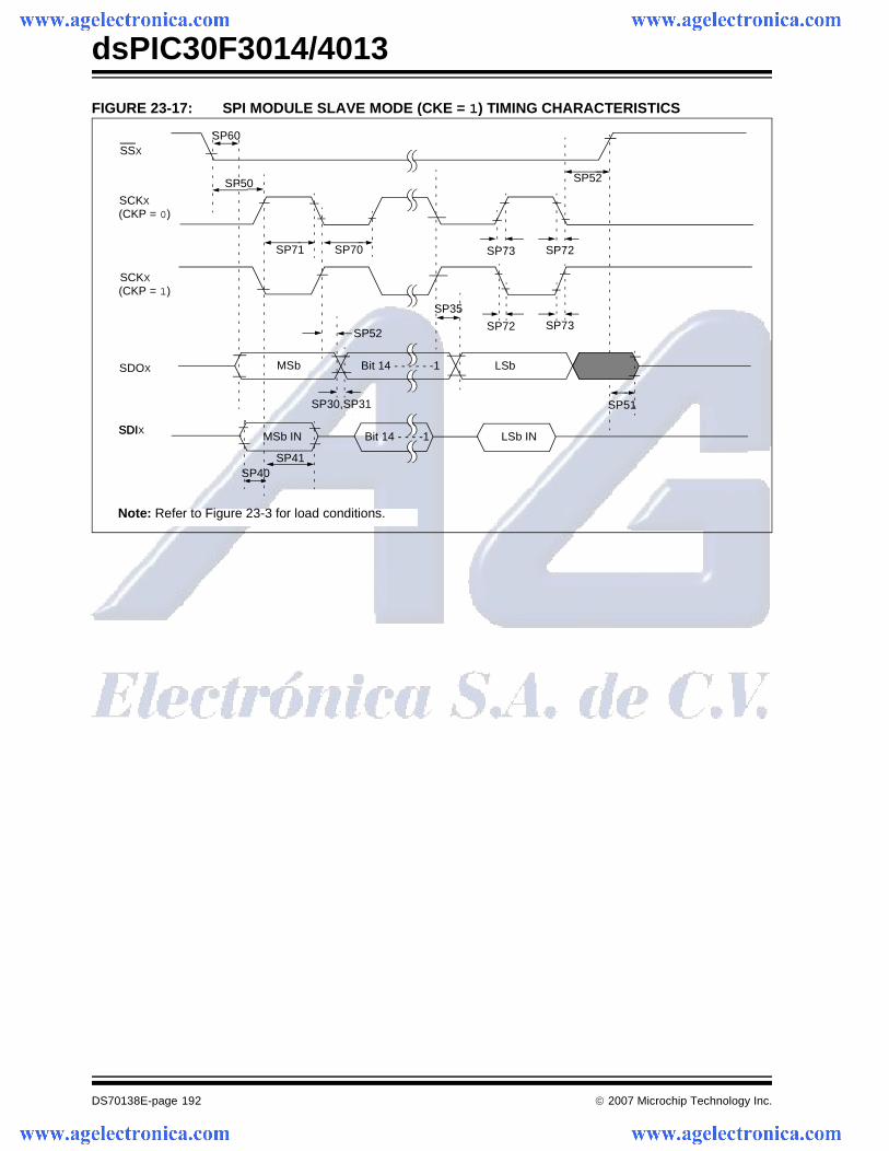
dsPIC30F3014/4013
DS70138E-page 192 © 2007 Microchip Technology Inc.
FIGURE 23-17: SPI MODULE SLAVE MODE (CKE = 1) TIMING CHARACTERISTICS
SSX
SCKX
(CKP = 0)
SCKX
(CKP = 1)
SDOX
SDI
SP50
SP60
SDIX
SP30,SP31
MSb Bit 14 - - - - - -1 LSb
SP51
MSb IN Bit 14 - - - -1 LSb IN
SP35
SP52
SP52
SP73SP72
SP72SP73SP71 SP70
SP40SP41
Note: Refer to Figure 23-3 for load conditions.
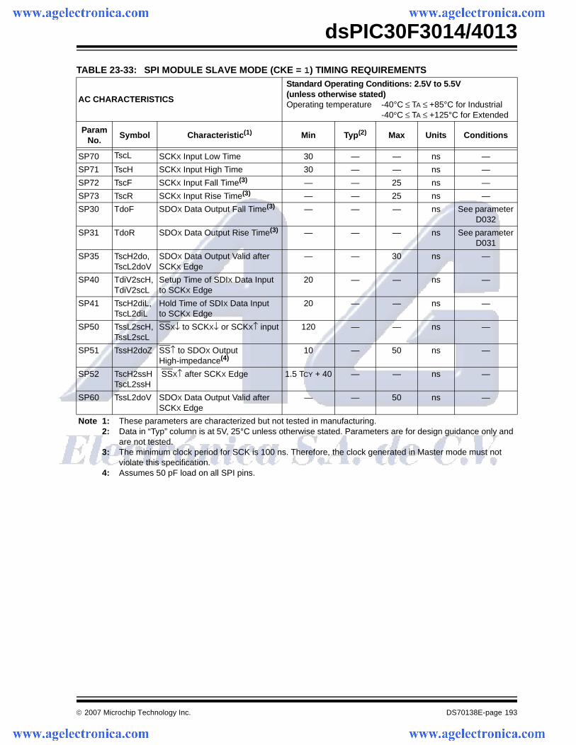
© 2007 Microchip Technology Inc. DS70138E-page 193
dsPIC30F3014/4013
TABLE 23-33: SPI MODULE SLAVE MODE (CKE = 1) TIMING REQUIREMENTS
AC CHARACTERISTICS
Standard Operating Conditions: 2.5V to 5.5V(unless otherwise stated)Operating temperature -40°C ≤ TA ≤ +85°C for Industrial
-40°C ≤ TA ≤ +125°C for Extended
ParamNo.
Symbol Characteristic(1) Min Typ(2) Max Units Conditions
SP70 TscL SCKX Input Low Time 30 — — ns —
SP71 TscH SCKX Input High Time 30 — — ns —
SP72 TscF SCKX Input Fall Time(3) — — 25 ns —
SP73 TscR SCKX Input Rise Time(3) — — 25 ns —
SP30 TdoF SDOX Data Output Fall Time(3) — — — ns See parameter D032
SP31 TdoR SDOX Data Output Rise Time(3) — — — ns See parameter D031
SP35 TscH2do,TscL2doV
SDOX Data Output Valid afterSCKX Edge
— — 30 ns —
SP40 TdiV2scH, TdiV2scL
Setup Time of SDIX Data Inputto SCKX Edge
20 — — ns —
SP41 TscH2diL, TscL2diL
Hold Time of SDIX Data Inputto SCKX Edge
20 — — ns —
SP50 TssL2scH, TssL2scL
SSX↓ to SCKX↓ or SCKX↑ input 120 — — ns —
SP51 TssH2doZ SS↑ to SDOX OutputHigh-impedance(4)
10 — 50 ns —
SP52 TscH2ssHTscL2ssH
SSX↑ after SCKX Edge 1.5 TCY + 40 — — ns —
SP60 TssL2doV SDOX Data Output Valid afterSCKX Edge
— — 50 ns —
Note 1: These parameters are characterized but not tested in manufacturing.2: Data in “Typ” column is at 5V, 25°C unless otherwise stated. Parameters are for design guidance only and
are not tested.3: The minimum clock period for SCK is 100 ns. Therefore, the clock generated in Master mode must not
violate this specification.4: Assumes 50 pF load on all SPI pins.
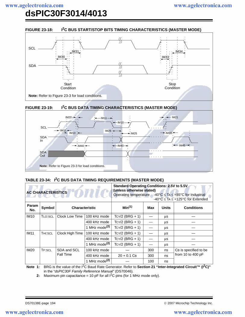
dsPIC30F3014/4013
DS70138E-page 194 © 2007 Microchip Technology Inc.
FIGURE 23-18: I2C BUS START/STOP BITS TIMING CHARACTERISTICS (MASTER MODE)
FIGURE 23-19: I2C BUS DATA TIMING CHARACTERISTICS (MASTER MODE)
TABLE 23-34: I2C BUS DATA TIMING REQUIREMENTS (MASTER MODE)
AC CHARACTERISTICS
Standard Operating Conditions: 2.5V to 5.5V(unless otherwise stated)Operating temperature -40°C ≤ TA ≤ +85°C for Industrial
-40°C ≤ TA ≤ +125°C for Extended
ParamNo.
Symbol Characteristic Min(1) Max Units Conditions
IM10 TLO:SCL Clock Low Time 100 kHz mode TCY/2 (BRG + 1) — μs —
400 kHz mode TCY/2 (BRG + 1) — μs —
1 MHz mode(2) TCY/2 (BRG + 1) — μs —
IM11 THI:SCL Clock High Time 100 kHz mode TCY/2 (BRG + 1) — μs —
400 kHz mode TCY/2 (BRG + 1) — μs —
1 MHz mode(2) TCY/2 (BRG + 1) — μs —
IM20 TF:SCL SDA and SCLFall Time
100 kHz mode — 300 ns CB is specified to be from 10 to 400 pF400 kHz mode 20 + 0.1 CB 300 ns
1 MHz mode(2) — 100 ns
Note 1: BRG is the value of the I2C Baud Rate Generator. Refer to Section 21 “Inter-Integrated Circuit™ (I2C)” in the “dsPIC30F Family Reference Manual” (DS70046).
2: Maximum pin capacitance = 10 pF for all I2C pins (for 1 MHz mode only).
IM31 IM34SCL
SDA
StartCondition
StopCondition
IM30 IM33
Note: Refer to Figure 23-3 for load conditions.
IM11IM10 IM33
IM11
IM10
IM20
IM26IM25
IM40 IM40 IM45
IM21
SCL
SDAIn
SDAOut
Note: Refer to Figure 23-3 for load conditions.
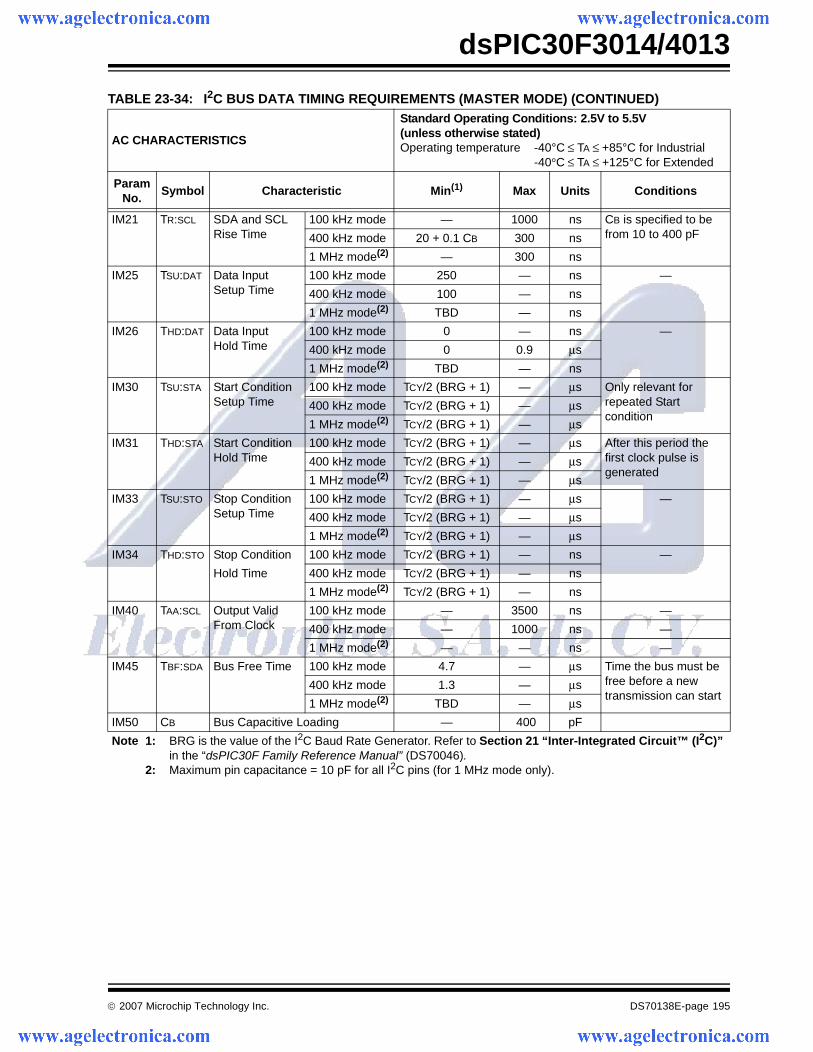
© 2007 Microchip Technology Inc. DS70138E-page 195
dsPIC30F3014/4013
IM21 TR:SCL SDA and SCLRise Time
100 kHz mode — 1000 ns CB is specified to be from 10 to 400 pF400 kHz mode 20 + 0.1 CB 300 ns
1 MHz mode(2) — 300 ns
IM25 TSU:DAT Data InputSetup Time
100 kHz mode 250 — ns —
400 kHz mode 100 — ns
1 MHz mode(2) TBD — ns
IM26 THD:DAT Data InputHold Time
100 kHz mode 0 — ns —
400 kHz mode 0 0.9 μs
1 MHz mode(2) TBD — ns
IM30 TSU:STA Start ConditionSetup Time
100 kHz mode TCY/2 (BRG + 1) — μs Only relevant for repeated Startcondition
400 kHz mode TCY/2 (BRG + 1) — μs
1 MHz mode(2) TCY/2 (BRG + 1) — μs
IM31 THD:STA Start Condition Hold Time
100 kHz mode TCY/2 (BRG + 1) — μs After this period thefirst clock pulse isgenerated
400 kHz mode TCY/2 (BRG + 1) — μs
1 MHz mode(2) TCY/2 (BRG + 1) — μs
IM33 TSU:STO Stop Condition Setup Time
100 kHz mode TCY/2 (BRG + 1) — μs —
400 kHz mode TCY/2 (BRG + 1) — μs
1 MHz mode(2) TCY/2 (BRG + 1) — μs
IM34 THD:STO Stop Condition 100 kHz mode TCY/2 (BRG + 1) — ns —
Hold Time 400 kHz mode TCY/2 (BRG + 1) — ns
1 MHz mode(2) TCY/2 (BRG + 1) — ns
IM40 TAA:SCL Output Valid From Clock
100 kHz mode — 3500 ns —
400 kHz mode — 1000 ns —
1 MHz mode(2) — — ns —
IM45 TBF:SDA Bus Free Time 100 kHz mode 4.7 — μs Time the bus must be free before a newtransmission can start
400 kHz mode 1.3 — μs
1 MHz mode(2) TBD — μs
IM50 CB Bus Capacitive Loading — 400 pF
TABLE 23-34: I2C BUS DATA TIMING REQUIREMENTS (MASTER MODE) (CONTINUED)
AC CHARACTERISTICS
Standard Operating Conditions: 2.5V to 5.5V(unless otherwise stated)Operating temperature -40°C ≤ TA ≤ +85°C for Industrial
-40°C ≤ TA ≤ +125°C for Extended
ParamNo.
Symbol Characteristic Min(1) Max Units Conditions
Note 1: BRG is the value of the I2C Baud Rate Generator. Refer to Section 21 “Inter-Integrated Circuit™ (I2C)” in the “dsPIC30F Family Reference Manual” (DS70046).
2: Maximum pin capacitance = 10 pF for all I2C pins (for 1 MHz mode only).
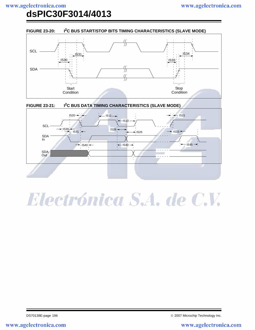
dsPIC30F3014/4013
DS70138E-page 196 © 2007 Microchip Technology Inc.
FIGURE 23-20: I2C BUS START/STOP BITS TIMING CHARACTERISTICS (SLAVE MODE)
FIGURE 23-21: I2C BUS DATA TIMING CHARACTERISTICS (SLAVE MODE)
IS31 IS34SCL
SDA
StartCondition
StopCondition
IS30 IS33
IS30IS31 IS33
IS11
IS10
IS20
IS26IS25
IS40 IS40 IS45
IS21
SCL
SDAIn
SDAOut
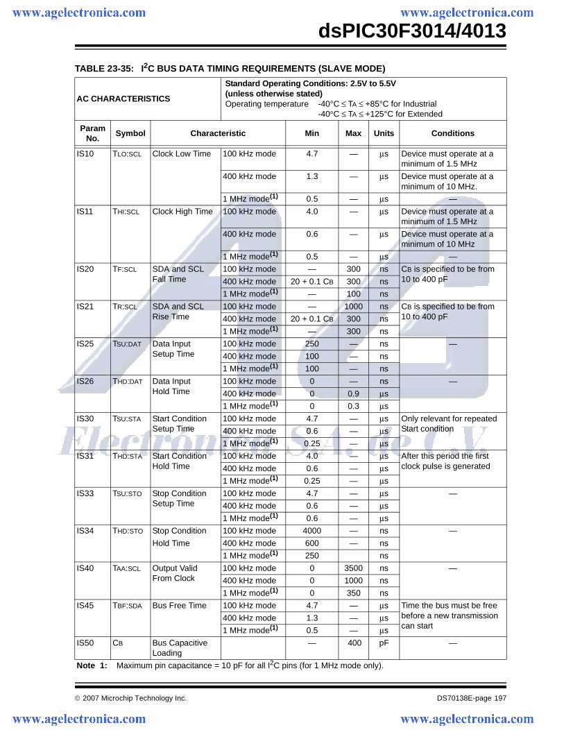
© 2007 Microchip Technology Inc. DS70138E-page 197
dsPIC30F3014/4013
TABLE 23-35: I2C BUS DATA TIMING REQUIREMENTS (SLAVE MODE)
AC CHARACTERISTICS
Standard Operating Conditions: 2.5V to 5.5V(unless otherwise stated)Operating temperature -40°C ≤ TA ≤ +85°C for Industrial
-40°C ≤ TA ≤ +125°C for Extended
ParamNo.
Symbol Characteristic Min Max Units Conditions
IS10 TLO:SCL Clock Low Time 100 kHz mode 4.7 — μs Device must operate at a minimum of 1.5 MHz
400 kHz mode 1.3 — μs Device must operate at a minimum of 10 MHz.
1 MHz mode(1) 0.5 — μs —
IS11 THI:SCL Clock High Time 100 kHz mode 4.0 — μs Device must operate at a minimum of 1.5 MHz
400 kHz mode 0.6 — μs Device must operate at a minimum of 10 MHz
1 MHz mode(1) 0.5 — μs —
IS20 TF:SCL SDA and SCLFall Time
100 kHz mode — 300 ns CB is specified to be from10 to 400 pF400 kHz mode 20 + 0.1 CB 300 ns
1 MHz mode(1) — 100 ns
IS21 TR:SCL SDA and SCLRise Time
100 kHz mode — 1000 ns CB is specified to be from10 to 400 pF400 kHz mode 20 + 0.1 CB 300 ns
1 MHz mode(1) — 300 ns
IS25 TSU:DAT Data InputSetup Time
100 kHz mode 250 — ns —
400 kHz mode 100 — ns
1 MHz mode(1) 100 — ns
IS26 THD:DAT Data InputHold Time
100 kHz mode 0 — ns —
400 kHz mode 0 0.9 μs
1 MHz mode(1) 0 0.3 μs
IS30 TSU:STA Start ConditionSetup Time
100 kHz mode 4.7 — μs Only relevant for repeated Start condition400 kHz mode 0.6 — μs
1 MHz mode(1) 0.25 — μs
IS31 THD:STA Start Condition Hold Time
100 kHz mode 4.0 — μs After this period the first clock pulse is generated400 kHz mode 0.6 — μs
1 MHz mode(1) 0.25 — μs
IS33 TSU:STO Stop Condition Setup Time
100 kHz mode 4.7 — μs —
400 kHz mode 0.6 — μs
1 MHz mode(1) 0.6 — μs
IS34 THD:STO Stop Condition 100 kHz mode 4000 — ns —
Hold Time 400 kHz mode 600 — ns
1 MHz mode(1) 250 ns
IS40 TAA:SCL Output Valid From Clock
100 kHz mode 0 3500 ns —
400 kHz mode 0 1000 ns
1 MHz mode(1) 0 350 ns
IS45 TBF:SDA Bus Free Time 100 kHz mode 4.7 — μs Time the bus must be free before a new transmission can start
400 kHz mode 1.3 — μs
1 MHz mode(1) 0.5 — μs
IS50 CB Bus Capacitive Loading
— 400 pF —
Note 1: Maximum pin capacitance = 10 pF for all I2C pins (for 1 MHz mode only).
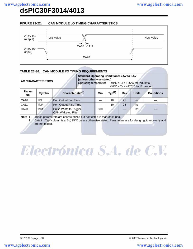
dsPIC30F3014/4013
DS70138E-page 198 © 2007 Microchip Technology Inc.
FIGURE 23-22: CAN MODULE I/O TIMING CHARACTERISTICS
TABLE 23-36: CAN MODULE I/O TIMING REQUIREMENTS
AC CHARACTERISTICS
Standard Operating Conditions: 2.5V to 5.5V(unless otherwise stated)Operating temperature -40°C ≤ TA ≤ +85°C for Industrial
-40°C ≤ TA ≤ +125°C for Extended
ParamNo.
Symbol Characteristic(1) Min Typ(2) Max Units Conditions
CA10 TioF Port Output Fall Time — 10 25 ns —
CA11 TioR Port Output Rise Time — 10 25 ns —
CA20 Tcwf Pulse Width to TriggerCAN Wake-up Filter
500 — — ns —
Note 1: These parameters are characterized but not tested in manufacturing.2: Data in “Typ” column is at 5V, 25°C unless otherwise stated. Parameters are for design guidance only and
are not tested.
CXTX Pin(output)
CA10 CA11
Old Value New Value
CA20
CXRX Pin(input)
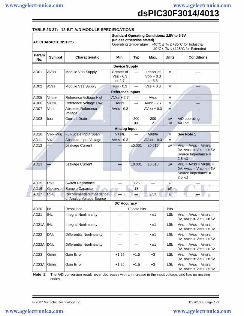
© 2007 Microchip Technology Inc. DS70138E-page 199
dsPIC30F3014/4013
TABLE 23-37: 12-BIT A/D MODULE SPECIFICATIONS
AC CHARACTERISTICS
Standard Operating Conditions: 2.5V to 5.5V(unless otherwise stated)Operating temperature -40°C ≤ TA ≤ +85°C for Industrial
-40°C ≤ TA ≤ +125°C for Extended
Param No.
Symbol Characteristic Min. Typ Max. Units Conditions
Device Supply
AD01 AVDD Module VDD Supply Greater ofVDD - 0.3
or 2.7
— Lesser ofVDD + 0.3
or 5.5
V —
AD02 AVSS Module VSS Supply VSS - 0.3 — VSS + 0.3 V —
Reference Inputs
AD05 VREFH Reference Voltage High AVSS + 2.7 — AVDD V —
AD06 VREFL Reference Voltage Low AVSS — AVDD - 2.7 V —
AD07 VREF Absolute ReferenceVoltage
AVSS - 0.3 — AVDD + 0.3 V —
AD08 IREF Current Drain — 200.001
3002
μAμA
A/D operatingA/D off
Analog Input
AD10 VINH-VINL Full-Scale Input Span VREFL — VREFH V See Note 1
AD11 VIN Absolute Input Voltage AVSS - 0.3 — AVDD + 0.3 V —
AD12 — Leakage Current — ±0.001 ±0.610 μA VINL = AVSS = VREFL = 0V, AVDD = VREFH = 5VSource Impedance =2.5 kΩ
AD13 — Leakage Current — ±0.001 ±0.610 μA VINL = AVSS = VREFL = 0V, AVDD = VREFH = 3VSource Impedance =2.5 kΩ
AD15 RSS Switch Resistance — 3.2K — Ω —
AD16 CSAMPLE Sample Capacitor — 18 pF —
AD17 RIN Recommended Impedance of Analog Voltage Source
— — 2.5K Ω —
DC Accuracy
AD20 Nr Resolution 12 data bits bits
AD21 INL Integral Nonlinearity — — <±1 LSb VINL = AVSS = VREFL = 0V, AVDD = VREFH = 5V
AD21A INL Integral Nonlinearity — — <±1 LSb VINL = AVSS = VREFL = 0V, AVDD = VREFH = 3V
AD22 DNL Differential Nonlinearity — — <±1 LSb VINL = AVSS = VREFL = 0V, AVDD = VREFH = 5V
AD22A DNL Differential Nonlinearity — — <±1 LSb VINL = AVSS = VREFL = 0V, AVDD = VREFH = 3V
AD23 GERR Gain Error +1.25 +1.5 +3 LSb VINL = AVSS = VREFL = 0V, AVDD = VREFH = 5V
AD23A GERR Gain Error +1.25 +1.5 +3 LSb VINL = AVSS = VREFL = 0V, AVDD = VREFH = 3V
Note 1: The A/D conversion result never decreases with an increase in the input voltage, and has no missing codes.
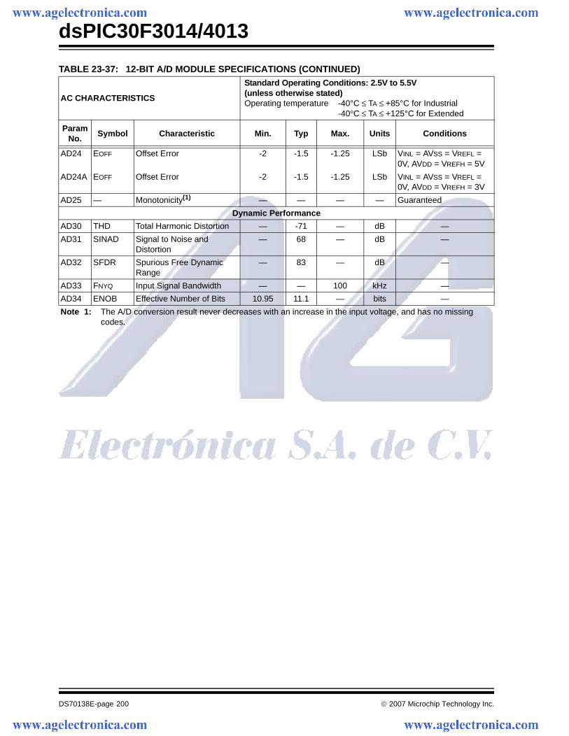
dsPIC30F3014/4013
DS70138E-page 200 © 2007 Microchip Technology Inc.
AD24 EOFF Offset Error -2 -1.5 -1.25 LSb VINL = AVSS = VREFL = 0V, AVDD = VREFH = 5V
AD24A EOFF Offset Error -2 -1.5 -1.25 LSb VINL = AVSS = VREFL = 0V, AVDD = VREFH = 3V
AD25 — Monotonicity(1) — — — — Guaranteed
Dynamic Performance
AD30 THD Total Harmonic Distortion — -71 — dB —
AD31 SINAD Signal to Noise andDistortion
— 68 — dB —
AD32 SFDR Spurious Free DynamicRange
— 83 — dB —
AD33 FNYQ Input Signal Bandwidth — — 100 kHz —
AD34 ENOB Effective Number of Bits 10.95 11.1 — bits —
TABLE 23-37: 12-BIT A/D MODULE SPECIFICATIONS (CONTINUED)
AC CHARACTERISTICS
Standard Operating Conditions: 2.5V to 5.5V(unless otherwise stated)Operating temperature -40°C ≤ TA ≤ +85°C for Industrial
-40°C ≤ TA ≤ +125°C for Extended
Param No.
Symbol Characteristic Min. Typ Max. Units Conditions
Note 1: The A/D conversion result never decreases with an increase in the input voltage, and has no missing codes.
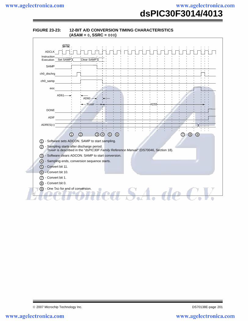
© 2007 Microchip Technology Inc. DS70138E-page 201
dsPIC30F3014/4013
FIGURE 23-23: 12-BIT A/D CONVERSION TIMING CHARACTERISTICS(ASAM = 0, SSRC = 000)
AD55TSAMP
Clear SAMPSet SAMP
AD61
ADCLK
Instruction
SAMP
ch0_dischrg
ch0_samp
AD60
DONE
ADIF
ADRES(0)
1 2 3 4 5 6 87
1 - Software sets ADCON. SAMP to start sampling.
2 - Sampling starts after discharge period.
3 - Software clears ADCON. SAMP to start conversion.
4 - Sampling ends, conversion sequence starts.
5 - Convert bit 11.
9 - One TAD for end of conversion.
AD50
eoc
9
6 - Convert bit 10.
7 - Convert bit 1.
8 - Convert bit 0.
Execution
TSAMP is described in the “dsPIC30F Family Reference Manual” (DS70046, Section 18).
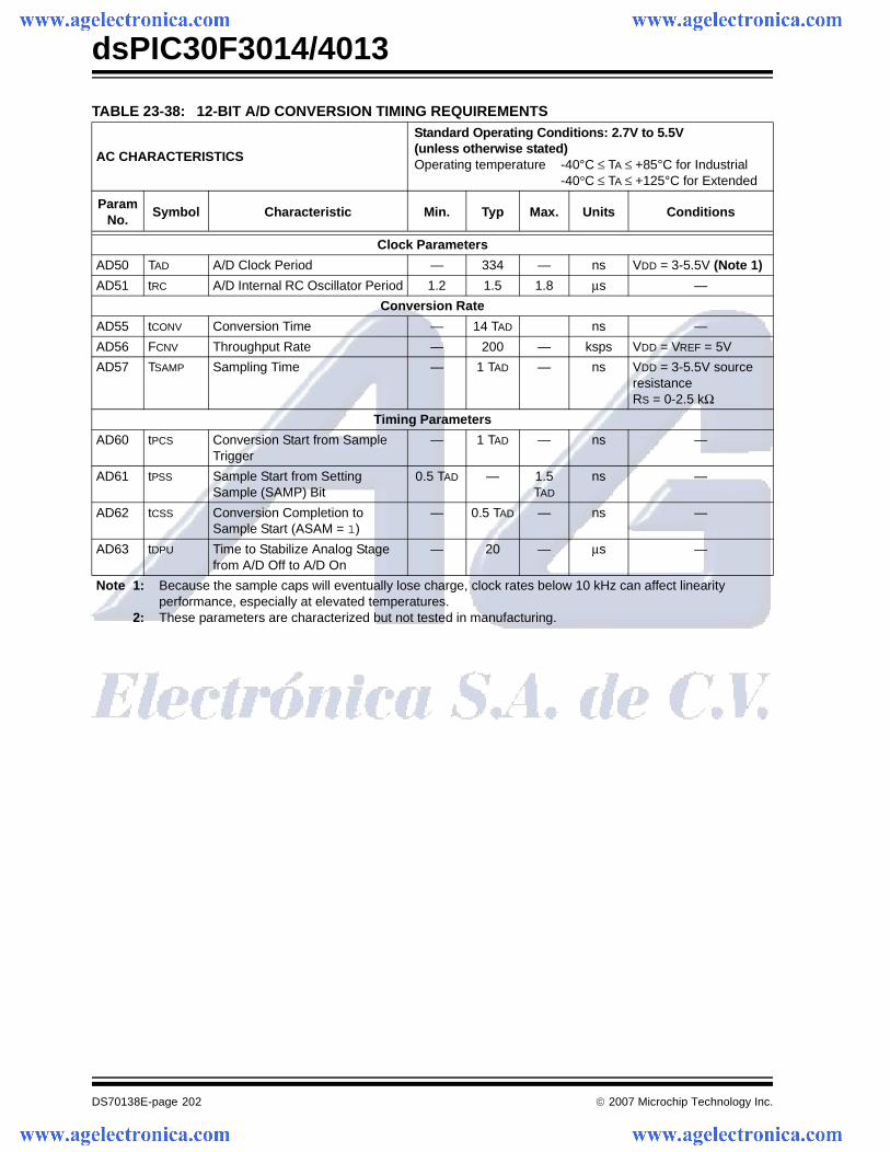
dsPIC30F3014/4013
DS70138E-page 202 © 2007 Microchip Technology Inc.
TABLE 23-38: 12-BIT A/D CONVERSION TIMING REQUIREMENTS
AC CHARACTERISTICS
Standard Operating Conditions: 2.7V to 5.5V(unless otherwise stated)Operating temperature -40°C ≤ TA ≤ +85°C for Industrial
-40°C ≤ TA ≤ +125°C for Extended
Param No.
Symbol Characteristic Min. Typ Max. Units Conditions
Clock Parameters
AD50 TAD A/D Clock Period — 334 — ns VDD = 3-5.5V (Note 1)
AD51 tRC A/D Internal RC Oscillator Period 1.2 1.5 1.8 μs —
Conversion Rate
AD55 tCONV Conversion Time — 14 TAD ns —
AD56 FCNV Throughput Rate — 200 — ksps VDD = VREF = 5V
AD57 TSAMP Sampling Time — 1 TAD — ns VDD = 3-5.5V source resistanceRS = 0-2.5 kΩ
Timing Parameters
AD60 tPCS Conversion Start from Sample Trigger
— 1 TAD — ns —
AD61 tPSS Sample Start from SettingSample (SAMP) Bit
0.5 TAD — 1.5 TAD
ns —
AD62 tCSS Conversion Completion toSample Start (ASAM = 1)
— 0.5 TAD — ns —
AD63 tDPU Time to Stabilize Analog Stagefrom A/D Off to A/D On
— 20 — μs —
Note 1: Because the sample caps will eventually lose charge, clock rates below 10 kHz can affect linearity performance, especially at elevated temperatures.
2: These parameters are characterized but not tested in manufacturing.
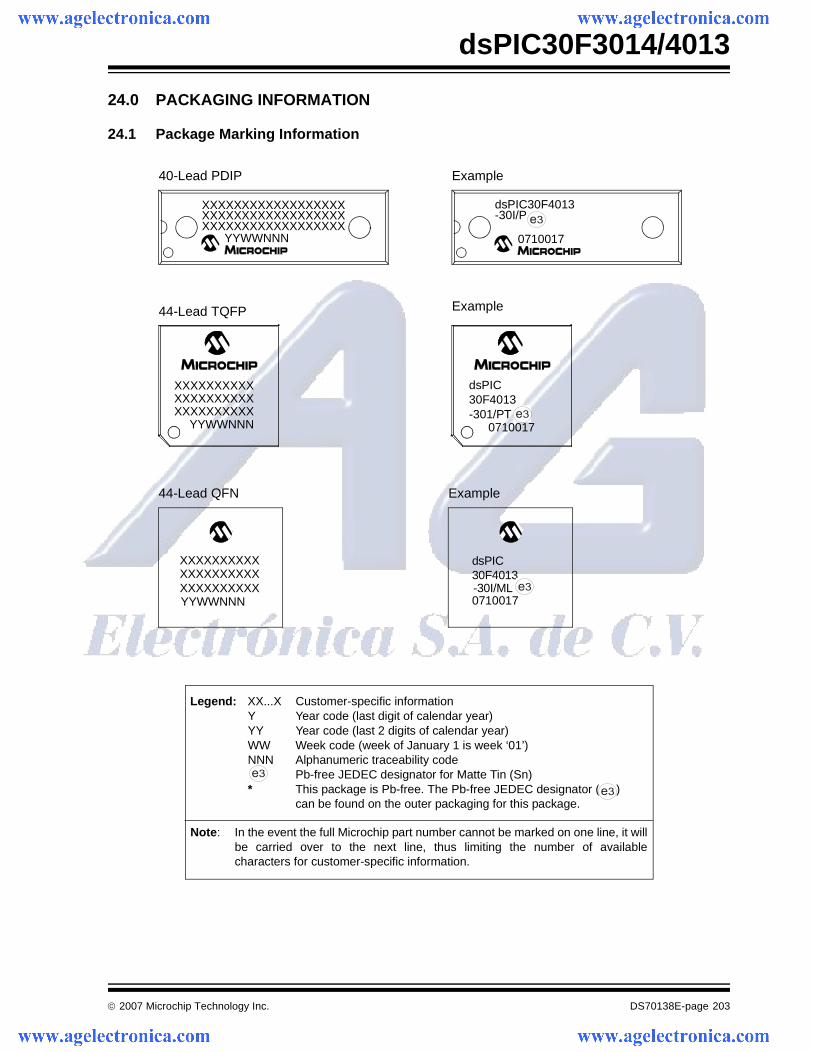
© 2007 Microchip Technology Inc. DS70138E-page 203
dsPIC30F3014/4013
24.0 PACKAGING INFORMATION
24.1 Package Marking Information
Example
dsPIC30F4013
0710017
40-Lead PDIP
XXXXXXXXXXXXXXXXXXXXXXXXXXXXXXXXXXXX
XXXXXXXXXXXXXXXXXXYYWWNNN
44-Lead TQFP
XXXXXXXXXXXXXXXXXXXXXXXXXXXXXX
YYWWNNN
Example
XXXXXXXXXX
44-Lead QFN
XXXXXXXXXXXXXXXXXXXXYYWWNNN
dsPIC
Example
0710017
0710017
dsPIC30F4013-301/PT
-30I/ML30F4013
-30I/P
Legend: XX...X Customer-specific informationY Year code (last digit of calendar year)YY Year code (last 2 digits of calendar year)WW Week code (week of January 1 is week ‘01’)NNN Alphanumeric traceability code Pb-free JEDEC designator for Matte Tin (Sn)* This package is Pb-free. The Pb-free JEDEC designator ( )
can be found on the outer packaging for this package.
Note: In the event the full Microchip part number cannot be marked on one line, it willbe carried over to the next line, thus limiting the number of availablecharacters for customer-specific information.
3e
3e
3e
3e
3e
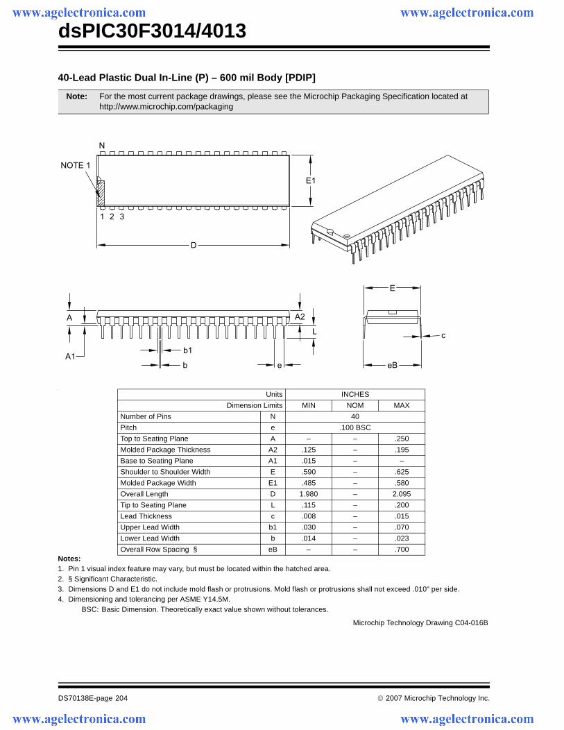
dsPIC30F3014/4013
DS70138E-page 204 © 2007 Microchip Technology Inc.
40-Lead Plastic Dual In-Line (P) – 600 mil Body [PDIP]
Notes:1. Pin 1 visual index feature may vary, but must be located within the hatched area.2. § Significant Characteristic.3. Dimensions D and E1 do not include mold flash or protrusions. Mold flash or protrusions shall not exceed .010" per side.4. Dimensioning and tolerancing per ASME Y14.5M.
BSC: Basic Dimension. Theoretically exact value shown without tolerances.
Note: For the most current package drawings, please see the Microchip Packaging Specification located at http://www.microchip.com/packaging
Units INCHES
Dimension Limits MIN NOM MAX
Number of Pins N 40
Pitch e .100 BSC
Top to Seating Plane A – – .250
Molded Package Thickness A2 .125 – .195
Base to Seating Plane A1 .015 – –
Shoulder to Shoulder Width E .590 – .625
Molded Package Width E1 .485 – .580
Overall Length D 1.980 – 2.095
Tip to Seating Plane L .115 – .200
Lead Thickness c .008 – .015
Upper Lead Width b1 .030 – .070
Lower Lead Width b .014 – .023
Overall Row Spacing § eB – – .700
N
NOTE 1
E1
D
1 2 3
A
A1b1
b e
c
eB
E
L
A2
Microchip Technology Drawing C04-016B
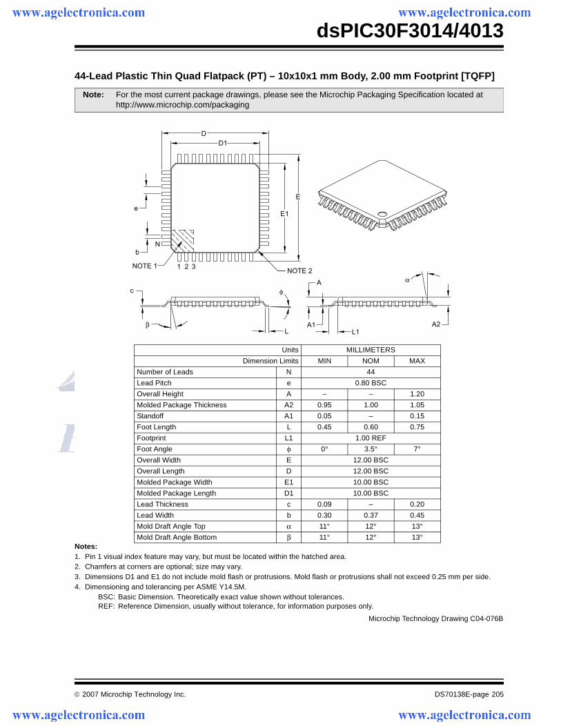
© 2007 Microchip Technology Inc. DS70138E-page 205
dsPIC30F3014/4013
44-Lead Plastic Thin Quad Flatpack (PT) – 10x10x1 mm Body, 2.00 mm Footprint [TQFP]
Notes:1. Pin 1 visual index feature may vary, but must be located within the hatched area.2. Chamfers at corners are optional; size may vary.3. Dimensions D1 and E1 do not include mold flash or protrusions. Mold flash or protrusions shall not exceed 0.25 mm per side.4. Dimensioning and tolerancing per ASME Y14.5M.
BSC: Basic Dimension. Theoretically exact value shown without tolerances.REF: Reference Dimension, usually without tolerance, for information purposes only.
Note: For the most current package drawings, please see the Microchip Packaging Specification located at http://www.microchip.com/packaging
Units MILLIMETERS
Dimension Limits MIN NOM MAX
Number of Leads N 44
Lead Pitch e 0.80 BSC
Overall Height A – – 1.20
Molded Package Thickness A2 0.95 1.00 1.05
Standoff A1 0.05 – 0.15
Foot Length L 0.45 0.60 0.75
Footprint L1 1.00 REF
Foot Angle φ 0° 3.5° 7°
Overall Width E 12.00 BSC
Overall Length D 12.00 BSC
Molded Package Width E1 10.00 BSC
Molded Package Length D1 10.00 BSC
Lead Thickness c 0.09 – 0.20
Lead Width b 0.30 0.37 0.45
Mold Draft Angle Top α 11° 12° 13°
Mold Draft Angle Bottom β 11° 12° 13°
A
E
E1
D
D1
e
b
NOTE 1NOTE 2
N
1 2 3
c
A1
L
A2
L1
α
φ
β
Microchip Technology Drawing C04-076B
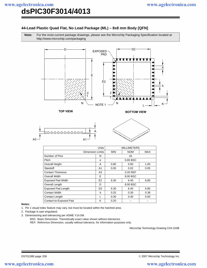
dsPIC30F3014/4013
DS70138E-page 206 © 2007 Microchip Technology Inc.
44-Lead Plastic Quad Flat, No Lead Package (ML) – 8x8 mm Body [QFN]
Notes:1. Pin 1 visual index feature may vary, but must be located within the hatched area.2. Package is saw singulated.3. Dimensioning and tolerancing per ASME Y14.5M.
BSC: Basic Dimension. Theoretically exact value shown without tolerances.REF: Reference Dimension, usually without tolerance, for information purposes only.
Note: For the most current package drawings, please see the Microchip Packaging Specification located at http://www.microchip.com/packaging
Units MILLIMETERS
Dimension Limits MIN NOM MAX
Number of Pins N 44
Pitch e 0.65 BSC
Overall Height A 0.80 0.90 1.00
Standoff A1 0.00 0.02 0.05
Contact Thickness A3 0.20 REF
Overall Width E 8.00 BSC
Exposed Pad Width E2 6.30 6.45 6.80
Overall Length D 8.00 BSC
Exposed Pad Length D2 6.30 6.45 6.80
Contact Width b 0.25 0.30 0.38
Contact Length L 0.30 0.40 0.50
Contact-to-Exposed Pad K 0.20 – –
DEXPOSED
PAD
D2
e
b
KL
E2
2
1
NNOTE 1
2
1
E
N
BOTTOM VIEWTOP VIEW
A3 A1
A
Microchip Technology Drawing C04-103B
© 2007 Microchip Technology Inc. DS70138E-page 207
dsPIC30F3014/4013
APPENDIX A: REVISION HISTORY
Revision D (June 2006)
Previous versions of this data sheet containedAdvance or Preliminary Information. They were distrib-uted with incomplete characterization data.
This revision reflects these changes:
• Revised I2C Slave Addresses (see Table 14-1)
• Updated example for ADC Conversion Clock selection (see Section 19.0 “12-bit Analog-to-Digital Converter (ADC) Module”)
• Base instruction CP1 eliminated from instruction set (seeTable 21-2 )
• Revised electrical characteristics:- Operating Current (IDD) Specifications
(see Table 23-5)- Idle Current (IIDLE) Specifications
(see Table 23-6)- Power-down Current (IPD) Specifications
(see Table 23-7)- I/O pin Input Specifications
(see Table 23-8)- Brown Out Reset (BOR) Specifications
(see Table 23-11)- Watchdog Timer time-out limits
(see Table 23-20)-
Revision E (January 2007)
This revision includes updates to the packaging diagrams.

dsPIC30F3014/4013
DS70138E-page 208 © 2007 Microchip Technology Inc.
NOTES:
© 2007 Microchip Technology Inc. DS70138E-page 209
dsPIC30F3014/4013
INDEX
Numerics12-bit Analog-to-Digital Converter (ADC) Module ............. 125
AA/D .................................................................................... 125
Aborting a Conversion .............................................. 127ADCHS Register ....................................................... 125ADCON1 Register..................................................... 125ADCON2 Register..................................................... 125ADCON3 Register..................................................... 125ADCSSL Register ..................................................... 125ADPCFG Register..................................................... 125Configuring Analog Port Pins.............................. 52, 132Connection Considerations....................................... 132Conversion Operation ............................................... 126Effects of a Reset...................................................... 131Operation During CPU Idle Mode ............................. 131Operation During CPU Sleep Mode.......................... 131Output Formats ......................................................... 131Power-down Modes .................................................. 131Programming the Sample Trigger............................. 127Register Map............................................................. 133Result Buffer ............................................................. 126Sampling Requirements............................................ 130Selecting the Conversion Sequence......................... 126
AC Characteristics ............................................................ 174Load Conditions ........................................................ 174
AC Temperature and Voltage Specifications .................... 174AC-Link Mode Operation .................................................. 122
16-bit Mode ............................................................... 12220-bit Mode ............................................................... 123
ADCSelecting the Conversion Clock ................................ 127
ADC Conversion Speeds .................................................. 128Address Generator Units .................................................... 35Alternate Vector Table ........................................................ 59Analog-to-Digital Converter. See A/D.Assembler
MPASM Assembler................................................... 162Automatic Clock Stretch...................................................... 88
During 10-bit Addressing (STREN = 1)....................... 88During 7-bit Addressing (STREN = 1)......................... 88Receive Mode ............................................................. 88Transmit Mode ............................................................ 88
BBandgap Start-up Time
Requirements............................................................ 180Timing Characteristics .............................................. 180
Barrel Shifter ....................................................................... 21Bit-Reversed Addressing .................................................... 38
Example ...................................................................... 38Implementation ........................................................... 38Modifier Values Table ................................................. 39Sequence Table (16-Entry)......................................... 39
Block Diagrams12-bit A/D Functional ................................................ 12516-bit Timer1 Module .................................................. 6316-bit Timer2............................................................... 6916-bit Timer3............................................................... 6916-bit Timer4............................................................... 7416-bit Timer5............................................................... 7432-bit Timer2/3............................................................ 68
32-bit Timer4/5 ........................................................... 73CAN Buffers and Protocol Engine ............................ 106DCI Module............................................................... 116Dedicated Port Structure ............................................ 51DSP Engine ................................................................ 18dsPIC30F3014.............................................................. 9dsPIC30F4013............................................................ 10External Power-on Reset Circuit .............................. 147I2C .............................................................................. 86Input Capture Mode.................................................... 77Oscillator System...................................................... 137Output Compare Mode ............................................... 81Reset System ........................................................... 145Shared Port Structure................................................. 52SPI.............................................................................. 94SPI Master/Slave Connection..................................... 94UART Receiver........................................................... 98UART Transmitter....................................................... 97
BOR Characteristics ......................................................... 173BOR. See Brown-out Reset.Brown-out Reset
Characteristics.......................................................... 172Timing Requirements ............................................... 180
CC Compilers
MPLAB C18.............................................................. 162MPLAB C30.............................................................. 162
CAN Module ..................................................................... 105Baud Rate Setting .................................................... 110CAN1 Register Map.................................................. 112Frame Types ............................................................ 105I/O Timing Characteristics ........................................ 198I/O Timing Requirements.......................................... 198Message Reception.................................................. 108Message Transmission............................................. 109Modes of Operation .................................................. 107Overview................................................................... 105
CLKO and I/O TimingCharacteristics.......................................................... 178Requirements ........................................................... 178
Code ExamplesData EEPROM Block Erase ....................................... 48Data EEPROM Block Write ........................................ 50Data EEPROM Read.................................................. 47Data EEPROM Word Erase ....................................... 48Data EEPROM Word Write ........................................ 49Erasing a Row of Program Memory ........................... 43Initiating a Programming Sequence ........................... 44Loading Write Latches................................................ 44
Code Protection................................................................ 135Control Registers ................................................................ 42
NVMADR .................................................................... 42NVMADRU ................................................................. 42NVMCON.................................................................... 42NVMKEY .................................................................... 42
Core ArchitectureOverview..................................................................... 13
CPU Architecture Overview................................................ 13Customer Change Notification Service............................. 215Customer Notification Service .......................................... 215Customer Support............................................................. 215
dsPIC30F3014/4013
DS70138E-page 210 © 2007 Microchip Technology Inc.
DData Accumulators and Adder/Subtracter........................... 19Data Accumulators and Adder/Subtractor
Data Space Write Saturation ...................................... 21Overflow and Saturation ............................................. 19Round Logic................................................................ 20Write-Back .................................................................. 20
Data Address Space ........................................................... 28Alignment .................................................................... 31Alignment (Figure) ...................................................... 31Effect of Invalid Memory Accesses (Table)................. 31MCU and DSP (MAC Class) Instructions Example..... 30Memory Map ......................................................... 28, 29Near Data Space ........................................................ 32Software Stack............................................................ 32Spaces ........................................................................ 31Width........................................................................... 31
Data Converter Interface (DCI) Module ............................ 115Data EEPROM Memory ...................................................... 47
Erasing........................................................................ 48Erasing, Block ............................................................. 48Erasing, Word ............................................................. 48Protection Against Spurious Write .............................. 50Reading....................................................................... 47Write Verify ................................................................. 50Writing......................................................................... 49Writing, Block .............................................................. 49Writing, Word .............................................................. 49
DC Characteristics ............................................................ 165BOR .......................................................................... 173Brown-out Reset ....................................................... 172I/O Pin Input Specifications ....................................... 171I/O Pin Output Specifications .................................... 171Idle Current (IIDLE) .................................................... 168Low-Voltage Detect................................................... 171LVDL ......................................................................... 172Operating Current (IDD)............................................. 167Power-Down Current (IPD) ........................................ 169Program and EEPROM............................................. 173Temperature and Voltage Specifications .................. 165
DCI ModuleBit Clock Generator................................................... 119Buffer Alignment with Data Frames .......................... 121Buffer Control ............................................................ 115Buffer Data Alignment ............................................... 115Buffer Length Control ................................................ 121COFS Pin.................................................................. 115CSCK Pin.................................................................. 115CSDI Pin ................................................................... 115CSDO Mode Bit ........................................................ 122CSDO Pin ................................................................. 115Data Justification Control Bit ..................................... 120Device Frequencies for Common Codec
CSCK Frequencies (Table)............................... 119Digital Loopback Mode ............................................. 122Enable....................................................................... 117Frame Sync Generator ............................................. 117Frame Sync Mode Control Bits ................................. 117I/O Pins ..................................................................... 115Interrupts................................................................... 122Introduction ............................................................... 115Master Frame Sync Operation.................................. 117Operation .................................................................. 117Operation During CPU Idle Mode ............................. 122Operation During CPU Sleep Mode.......................... 122
Receive Slot Enable Bits .......................................... 120Receive Status Bits................................................... 121Register Map ............................................................ 124Sample Clock Edge Control Bit ................................ 120Slave Frame Sync Operation.................................... 118Slot Enable Bits Operation with Frame Sync............ 120Slot Status Bits ......................................................... 122Synchronous Data Transfers .................................... 120Timing Characteristics
AC-Link Mode................................................... 187Multichannel, I2S Modes................................... 185
Timing RequirementsAC-Link Mode................................................... 188Multichannel, I2S Modes................................... 185
Transmit Slot Enable Bits ......................................... 120Transmit Status Bits.................................................. 121Transmit/Receive Shift Register ............................... 115Underflow Mode Control Bit...................................... 122Word Size Selection Bits .......................................... 117
Development Support ....................................................... 161Device Configuration
Register Map ............................................................ 152Device Configuration Registers
FBORPOR................................................................ 150FGS .......................................................................... 150FOSC........................................................................ 150FWDT ....................................................................... 150
Device Overview................................................................... 9Disabling the UART ............................................................ 99Divide Support .................................................................... 16
Instructions (Table) ..................................................... 16DSP Engine ........................................................................ 17
Multiplier ..................................................................... 19Dual Output Compare Match Mode .................................... 82
Continuous Pulse Mode.............................................. 82Single Pulse Mode...................................................... 82
EElectrical Characteristics .................................................. 165
AC............................................................................. 174DC ............................................................................ 165
Enabling and Setting Up UARTAlternate I/O ............................................................... 99Setting Up Data, Parity and Stop Bit Selections ......... 99
Enabling the UART ............................................................. 99Equations
ADC Conversion Clock ............................................. 127Baud Rate................................................................. 101Bit Clock Frequency.................................................. 119COFSG Period.......................................................... 117Serial Clock Rate ........................................................ 90Time Quantum for Clock Generation ........................ 111
Errata .................................................................................... 7Exception Sequence
Trap Sources .............................................................. 58External Clock Timing Characteristics
Type A, B and C Timer ............................................. 181External Clock Timing Requirements ............................... 175
Type A Timer ............................................................ 181Type B Timer ............................................................ 182Type C Timer ............................................................ 182
External Interrupt Requests ................................................ 60
FFast Context Saving ........................................................... 60Flash Program Memory ...................................................... 41
© 2007 Microchip Technology Inc. DS70138E-page 211
dsPIC30F3014/4013
II/O Pin Specifications
Input .......................................................................... 171Output ....................................................................... 171
I/O Ports .............................................................................. 51Parallel (PIO) .............................................................. 51
I2C 10-bit Slave Mode Operation ........................................ 87Reception.................................................................... 88Transmission............................................................... 87
I2C 7-bit Slave Mode Operation .......................................... 87Reception.................................................................... 87Transmission............................................................... 87
I2C Master Mode Operation ................................................ 89Baud Rate Generator.................................................. 90Clock Arbitration.......................................................... 90Multi-Master Communication, Bus Collision and
Bus Arbitration .................................................... 90Reception.................................................................... 90Transmission............................................................... 89
I2C Master Mode Support ................................................... 89I2C Module .......................................................................... 85
Addresses ................................................................... 87Bus Data Timing Characteristics
Master Mode..................................................... 194Slave Mode....................................................... 196
Bus Data Timing RequirementsMaster Mode..................................................... 194Slave Mode....................................................... 197
Bus Start/Stop Bits Timing CharacteristicsMaster Mode..................................................... 194Slave Mode....................................................... 196
General Call Address Support .................................... 89Interrupts..................................................................... 89IPMI Support ............................................................... 89Operating Function Description .................................. 85Operation During CPU Sleep and Idle Modes ............ 90Pin Configuration ........................................................ 85Programmer’s Model................................................... 85Register Map............................................................... 91Registers..................................................................... 85Slope Control .............................................................. 89Software Controlled Clock Stretching (STREN = 1).... 88Various Modes ............................................................ 85
I2S Mode Operation .......................................................... 123Data Justification....................................................... 123Frame and Data Word Length Selection................... 123
Idle Current (IIDLE) ............................................................ 168In-Circuit Serial Programming (ICSP) ......................... 41, 135Input Capture (CAPX) Timing Characteristics .................. 183Input Capture Module ......................................................... 77
Interrupts..................................................................... 78Register Map............................................................... 79
Input Capture Operation During Sleep and Idle Modes ...... 78CPU Idle Mode............................................................ 78CPU Sleep Mode ........................................................ 78
Input Capture Timing Requirements ................................. 183Input Change Notification Module....................................... 54
dsPIC30F3014 Register Map (Bits 15-8) .................... 54dsPIC30F3014 Register Map (Bits 7-0) ...................... 54dsPIC30F4013 Register Map (Bits 15-8) .................... 54dsPIC30F4013 Register Map (Bits 7-0) ...................... 54
Instruction Addressing Modes............................................. 35File Register Instructions ............................................ 35Fundamental Modes Supported.................................. 35MAC Instructions......................................................... 36
MCU Instructions ........................................................ 35Move and Accumulator Instructions ........................... 36Other Instructions ....................................................... 36
Instruction SetOverview................................................................... 156Summary .................................................................. 153
Internal Clock Timing Examples ....................................... 176Internet Address ............................................................... 215Interrupt Controller
Register Map .............................................................. 62Interrupt Priority .................................................................. 56
Traps .......................................................................... 58Interrupt Sequence ............................................................. 59
Interrupt Stack Frame................................................. 59Interrupts ............................................................................ 55
LLoad Conditions................................................................ 174Low-Voltage Detect (LVD)................................................ 149Low-Voltage Detect Characteristics.................................. 171LVDL Characteristics ........................................................ 172
MMemory Organization ......................................................... 23
Core Register Map ..................................................... 32Microchip Internet Web Site.............................................. 215Modes of Operation
Disable...................................................................... 107Initialization............................................................... 107Listen All Messages.................................................. 107Listen Only................................................................ 107Loopback .................................................................. 107Normal Operation ..................................................... 107
Modulo Addressing ............................................................. 36Applicability................................................................. 38Incrementing Buffer Operation Example .................... 37Start and End Address ............................................... 37W Address Register Selection.................................... 37
MPLAB ASM30 Assembler, Linker, Librarian ................... 162MPLAB ICD 2 In-Circuit Debugger ................................... 163MPLAB ICE 2000 High-Performance Universal
In-Circuit Emulator.................................................... 163MPLAB ICE 4000 High-Performance Universal
In-Circuit Emulator.................................................... 163MPLAB Integrated Development Environment Software.. 161MPLAB PM3 Device Programmer .................................... 163MPLINK Object Linker/MPLIB Object Librarian ................ 162
NNVM
Register Map .............................................................. 45
OOC/PWM Module Timing Characteristics ......................... 184Operating Current (IDD) .................................................... 167Operating Frequency vs Voltage
dsPIC30FXXXX-20 (Extended) ................................ 165Oscillator
Configurations .......................................................... 138Fail-Safe Clock Monitor .................................... 140Fast RC (FRC).................................................. 139Initial Clock Source Selection........................... 138Low-Power RC (LPRC) .................................... 139LP Oscillator Control......................................... 139Phase Locked Loop (PLL) ................................ 139Start-up Timer (OST)........................................ 138
dsPIC30F3014/4013
DS70138E-page 212 © 2007 Microchip Technology Inc.
Control Registers ...................................................... 141Operating Modes (Table) .......................................... 136System Overview ...................................................... 135
Oscillator Selection ........................................................... 135Oscillator Start-up Timer
Timing Characteristics .............................................. 179Timing Requirements................................................ 180
Output Compare Interrupts ................................................. 83Output Compare Module..................................................... 81
Register Map dsPIC30F3014...................................... 84Register Map dsPIC30F4013...................................... 84Timing Characteristics .............................................. 183Timing Requirements................................................ 183
Output Compare Operation During CPU Idle Mode............ 83Output Compare Sleep Mode Operation............................. 83
PPackaging Information ...................................................... 203
Marking ..................................................................... 203Peripheral Module Disable (PMD) Registers .................... 151PICSTART Plus Development Programmer ..................... 164Pinout Descriptions ............................................................. 11POR. See Power-on Reset.Port Register Map for dsPIC30F3014/4013 ........................ 53Port Write/Read Example.................................................... 52Power Saving Modes
Sleep and Idle ........................................................... 135Power-Down Current (IPD) ................................................ 169Power-Saving Modes ........................................................ 149
Idle ............................................................................ 150Sleep......................................................................... 149
Power-up TimerTiming Characteristics .............................................. 179Timing Requirements................................................ 180
Program Address Space ..................................................... 23Construction................................................................ 24Data Access from Program Memory Using
Program Space Visibility ..................................... 26Data Access From Program Memory Using
Table Instructions................................................ 25Data Access from, Address Generation...................... 24Data Space Window into Operation ............................ 27Data Table Access (lsw) ............................................. 25Data Table Access (MS Byte) ..................................... 26Memory Map ............................................................... 23Table Instructions
TBLRDH.............................................................. 25TBLRDL .............................................................. 25TBLWTH ............................................................. 25TBLWTL.............................................................. 25
Program and EEPROM Characteristics ............................ 173Program Counter................................................................. 14Programmable................................................................... 135Programmer’s Model........................................................... 14
Diagram ...................................................................... 15Programming Operations .................................................... 43
Algorithm for Program Flash ....................................... 43Erasing a Row of Program Memory ............................ 43Initiating the Programming Sequence......................... 44Loading Write Latches ................................................ 44
Protection Against Accidental Writes to OSCCON ........... 140
RReader Response............................................................. 216Reset ........................................................................ 135, 145
BOR, Programmable ................................................ 147Brown-out Reset (BOR)............................................ 135Oscillator Start-up Timer (OST) ................................ 135POR
Operating without FSCM and PWRT................ 147With Long Crystal Start-up Time ...................... 147
POR (Power-on Reset)............................................. 145Power-on Reset (POR)............................................. 135Power-up Timer (PWRT) .......................................... 135
Reset Sequence ................................................................. 57Reset Sources ............................................................ 57
Reset SourcesBrown-out Reset (BOR).............................................. 57Illegal Instruction Trap ................................................ 57Trap Lockout............................................................... 57Uninitialized W Register Trap ..................................... 57Watchdog Time-out .................................................... 57
Reset Timing Characteristics............................................ 179Reset Timing Requirements ............................................. 180Run-Time Self-Programming (RTSP) ................................. 41
SSimple Capture Event Mode............................................... 77
Buffer Operation ......................................................... 78Hall Sensor Mode ....................................................... 78Prescaler .................................................................... 77Timer2 and Timer3 Selection Mode............................ 78
Simple OC/PWM Mode Timing Requirements ................. 184Simple Output Compare Match Mode ................................ 82Simple PWM Mode ............................................................. 82
Input Pin Fault Protection ........................................... 82Period ......................................................................... 83
Software Simulator (MPLAB SIM) .................................... 162Software Stack Pointer, Frame Pointer .............................. 14
CALL Stack Frame ..................................................... 32SPI Module ......................................................................... 93
Framed SPI Support ................................................... 93Operating Function Description .................................. 93Operation During CPU Idle Mode............................... 95Operation During CPU Sleep Mode............................ 95SDOx Disable ............................................................. 93Slave Select Synchronization ..................................... 95SPI1 Register Map...................................................... 96Timing Characteristics
Master Mode (CKE = 0).................................... 189Master Mode (CKE = 1).................................... 190Slave Mode (CKE = 1).............................. 191, 192
Timing RequirementsMaster Mode (CKE = 0).................................... 189Master Mode (CKE = 1).................................... 190Slave Mode (CKE = 0)...................................... 191Slave Mode (CKE = 1)...................................... 193
Word and Byte Communication .................................. 93Status Bits, Their Significance and the Initialization
Condition for RCON Register, Case 1 ...................... 148Status Bits, Their Significance and the Initialization
Condition for RCON Register, Case 2 ...................... 148Status Register ................................................................... 14Symbols Used in Opcode Descriptions ............................ 154System Integration............................................................ 135
Register Map ............................................................ 152
© 2007 Microchip Technology Inc. DS70138E-page 213
dsPIC30F3014/4013
TTable Instruction Operation Summary ................................ 41Temperature and Voltage Specifications
AC ............................................................................. 174DC............................................................................. 165
Timer1 Module .................................................................... 6316-bit Asynchronous Counter Mode ........................... 6316-bit Synchronous Counter Mode ............................. 6316-bit Timer Mode....................................................... 63Gate Operation ........................................................... 64Interrupt....................................................................... 64Operation During Sleep Mode .................................... 64Prescaler..................................................................... 64Real-Time Clock ......................................................... 64
Interrupts............................................................. 65Oscillator Operation ............................................ 65
Register Map............................................................... 66Timer2 and Timer3 Selection Mode.................................... 81Timer2/3 Module ................................................................. 67
16-bit Timer Mode....................................................... 6732-bit Synchronous Counter Mode ............................. 6732-bit Timer Mode....................................................... 67ADC Event Trigger...................................................... 70Gate Operation ........................................................... 70Interrupt....................................................................... 70Operation During Sleep Mode .................................... 70Register Map............................................................... 71Timer Prescaler........................................................... 70
Timer4/5 Module ................................................................. 73Register Map............................................................... 75
Timing CharacteristicsA/D Conversion
Low-speed (ASAM = 0, SSRC = 000) .............. 201Bandgap Start-up Time............................................. 180CAN Module I/O........................................................ 198CLKO and I/O ........................................................... 178DCI Module
AC-Link Mode ................................................... 187Multichannel, I2S Modes................................... 185
External Clock........................................................... 174I2C Bus Data
Master Mode..................................................... 194Slave Mode....................................................... 196
I2C Bus Start/Stop BitsMaster Mode..................................................... 194Slave Mode....................................................... 196
Input Capture (CAPX) ............................................... 183OC/PWM Module ...................................................... 184Oscillator Start-up Timer ........................................... 179Output Compare Module........................................... 183Power-up Timer ........................................................ 179Reset......................................................................... 179SPI Module
Master Mode (CKE = 0) .................................... 189Master Mode (CKE = 1) .................................... 190Slave Mode (CKE = 0) ...................................... 191Slave Mode (CKE = 1) ...................................... 192
Type A, B and C Timer External Clock ..................... 181Watchdog Timer........................................................ 179
Timing DiagramsCAN Bit ..................................................................... 110Frame Sync, AC-Link Start-of-Frame ....................... 118Frame Sync, Multichannel Mode .............................. 118I2S Interface Frame Sync.......................................... 118PWM Output ............................................................... 83
Time-out Sequence on Power-up (MCLR Not Tied to VDD), Case 1.................................. 146
Time-out Sequence on Power-up (MCLR Not Tied to VDD), Case 2.................................. 146
Time-out Sequence on Power-up (MCLR Tied to VDD).............................................................. 146
Timing Diagrams and SpecificationsDC Characteristics - Internal RC Accuracy .............. 176
Timing Diagrams.See Timing CharacteristicsTiming Requirements
A/D ConversionLow-speed........................................................ 202
Bandgap Start-up Time ............................................ 180Brown-out Reset....................................................... 180CAN Module I/O ....................................................... 198CLKO and I/O ........................................................... 178DCI Module
AC-Link Mode................................................... 188Multichannel, I2S Modes................................... 185
External Clock .......................................................... 175I2C Bus Data (Master Mode) .................................... 194I2C Bus Data (Slave Mode) ...................................... 197Input Capture............................................................ 183Oscillator Start-up Timer........................................... 180Output Compare Module .......................................... 183Power-up Timer ........................................................ 180Reset ........................................................................ 180Simple OC/PWM Mode ............................................ 184SPI Module
Master Mode (CKE = 0).................................... 189Master Mode (CKE = 1).................................... 190Slave Mode (CKE = 0)...................................... 191Slave Mode (CKE = 1)...................................... 193
Type A Timer External Clock.................................... 181Type B Timer External Clock.................................... 182Type C Timer External Clock.................................... 182Watchdog Timer ....................................................... 180
Trap Vectors ....................................................................... 59
UUART Module
Address Detect Mode ............................................... 101Auto Baud Support ................................................... 102Baud Rate Generator ............................................... 101Enabling and Setting Up............................................. 99Framing Error (FERR) .............................................. 101Idle Status................................................................. 101Loopback Mode ........................................................ 101Operation During CPU Sleep and Idle Modes.......... 102Overview..................................................................... 97Parity Error (PERR) .................................................. 101Receive Break .......................................................... 101Receive Buffer (UxRXB)........................................... 100Receive Buffer Overrun Error (OERR Bit) ................ 100Receive Interrupt ...................................................... 100Receiving Data ......................................................... 100Receiving in 8-bit or 9-bit Data Mode ....................... 100Reception Error Handling ......................................... 100Transmit Break ......................................................... 100Transmit Buffer (UxTXB) ............................................ 99Transmit Interrupt ..................................................... 100Transmitting Data ....................................................... 99Transmitting in 8-Bit Data Mode ................................. 99Transmitting in 9-bit Data Mode ................................. 99UART1 Register Map ............................................... 103UART2 Register Map ............................................... 103
dsPIC30F3014/4013
DS70138E-page 214 © 2007 Microchip Technology Inc.
UART OperationIdle Mode .................................................................. 102Sleep Mode............................................................... 102
Unit ID Locations............................................................... 135Universal Asynchronous Receiver Transmitter
(UART) Module ........................................................... 97
WWake-up from Sleep ......................................................... 135Wake-up from Sleep and Idle.............................................. 60Watchdog Timer
Timing Characteristics .............................................. 179Timing Requirements................................................ 180
Watchdog Timer (WDT) ............................................ 135, 149Enabling and Disabling ............................................. 149Operation .................................................................. 149
WWW Address.................................................................. 215WWW, On-Line Support........................................................ 7

© 2007 Microchip Technology Inc. DS70138E-page 215
dsPIC30F3014/4013
THE MICROCHIP WEB SITE
Microchip provides online support via our WWW site atwww.microchip.com. This web site is used as a meansto make files and information easily available tocustomers. Accessible by using your favorite Internetbrowser, the web site contains the followinginformation:
• Product Support – Data sheets and errata, application notes and sample programs, design resources, user’s guides and hardware support documents, latest software releases and archived software
• General Technical Support – Frequently Asked Questions (FAQ), technical support requests, online discussion groups, Microchip consultant program member listing
• Business of Microchip – Product selector and ordering guides, latest Microchip press releases, listing of seminars and events, listings of Microchip sales offices, distributors and factory representatives
CUSTOMER CHANGE NOTIFICATION SERVICE
Microchip’s customer notification service helps keepcustomers current on Microchip products. Subscriberswill receive e-mail notification whenever there arechanges, updates, revisions or errata related to aspecified product family or development tool of interest.
To register, access the Microchip web site atwww.microchip.com, click on Customer ChangeNotification and follow the registration instructions.
CUSTOMER SUPPORT
Users of Microchip products can receive assistancethrough several channels:
• Distributor or Representative
• Local Sales Office• Field Application Engineer (FAE)• Technical Support
• Development Systems Information Line
Customers should contact their distributor,representative or field application engineer (FAE) forsupport. Local sales offices are also available to helpcustomers. A listing of sales offices and locations isincluded in the back of this document.
Technical support is available through the web siteat: http://support.microchip.com

dsPIC30F3014/4013
DS70138E-page 216 © 2007 Microchip Technology Inc.
READER RESPONSE
It is our intention to provide you with the best documentation possible to ensure successful use of your Microchip prod-uct. If you wish to provide your comments on organization, clarity, subject matter, and ways in which our documentationcan better serve you, please FAX your comments to the Technical Publications Manager at (480) 792-4150.
Please list the following information, and use this outline to provide us with your comments about this document.
To: Technical Publications Manager
RE: Reader Response
Total Pages Sent ________
From: Name
Company
Address
City / State / ZIP / Country
Telephone: (_______) _________ - _________
Application (optional):
Would you like a reply? Y N
Device: Literature Number:
Questions:
FAX: (______) _________ - _________
DS70138EdsPIC30F3014/4013
1. What are the best features of this document?
2. How does this document meet your hardware and software development needs?
3. Do you find the organization of this document easy to follow? If not, why?
4. What additions to the document do you think would enhance the structure and subject?
5. What deletions from the document could be made without affecting the overall usefulness?
6. Is there any incorrect or misleading information (what and where)?
7. How would you improve this document?
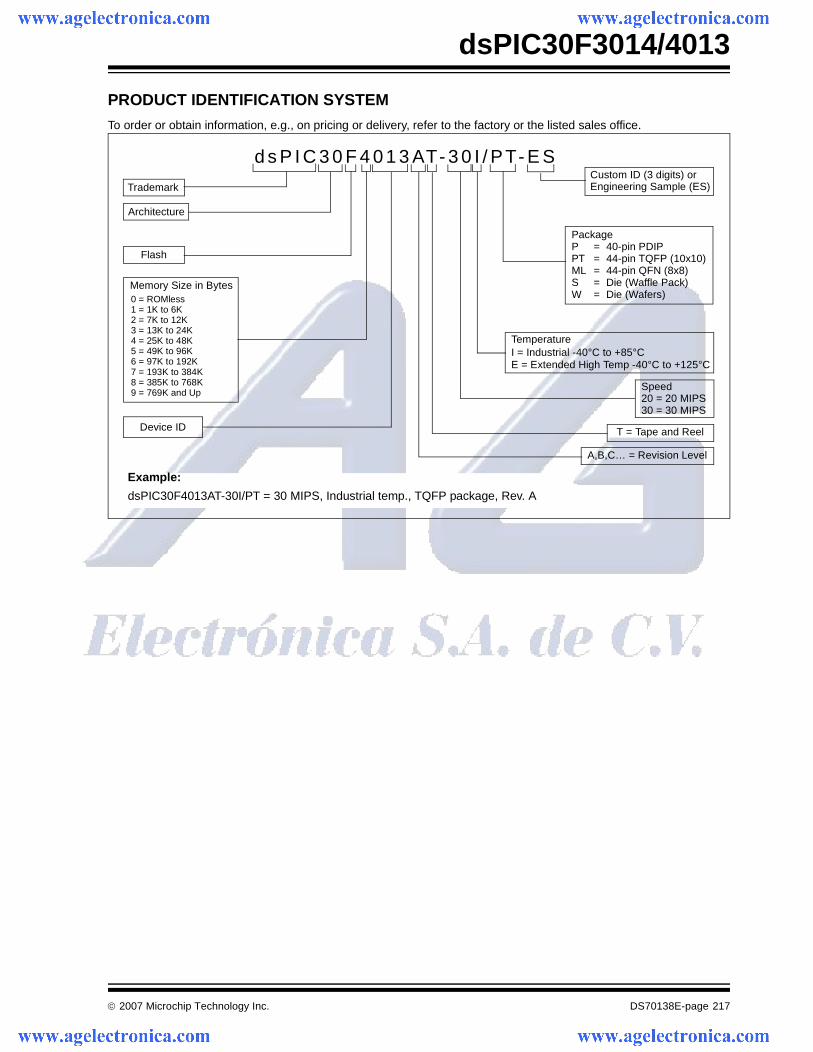
© 2007 Microchip Technology Inc. DS70138E-page 217
dsPIC30F3014/4013
PRODUCT IDENTIFICATION SYSTEM
To order or obtain information, e.g., on pricing or delivery, refer to the factory or the listed sales office.
d s P I C 3 0 F 4 0 1 3 AT- 3 0 I / PT- E S
Example:
dsPIC30F4013AT-30I/PT = 30 MIPS, Industrial temp., TQFP package, Rev. A
Trademark
Architecture
Flash
E = Extended High Temp -40°C to +125°CI = Industrial -40°C to +85°CTemperature
Device ID
Memory Size in Bytes0 = ROMless1 = 1K to 6K2 = 7K to 12K3 = 13K to 24K4 = 25K to 48K5 = 49K to 96K6 = 97K to 192K7 = 193K to 384K8 = 385K to 768K9 = 769K and Up
Custom ID (3 digits) or
T = Tape and Reel
A,B,C… = Revision Level
Engineering Sample (ES)
Speed20 = 20 MIPS30 = 30 MIPS
PackageP = 40-pin PDIPPT = 44-pin TQFP (10x10)ML = 44-pin QFN (8x8)S = Die (Waffle Pack)W = Die (Wafers)