Embed Size (px)
Citation preview
User Manual
DSP6000A Digital Studio-Transmitter Link
Doc. 602-11157-01 R: A
Released August 1997

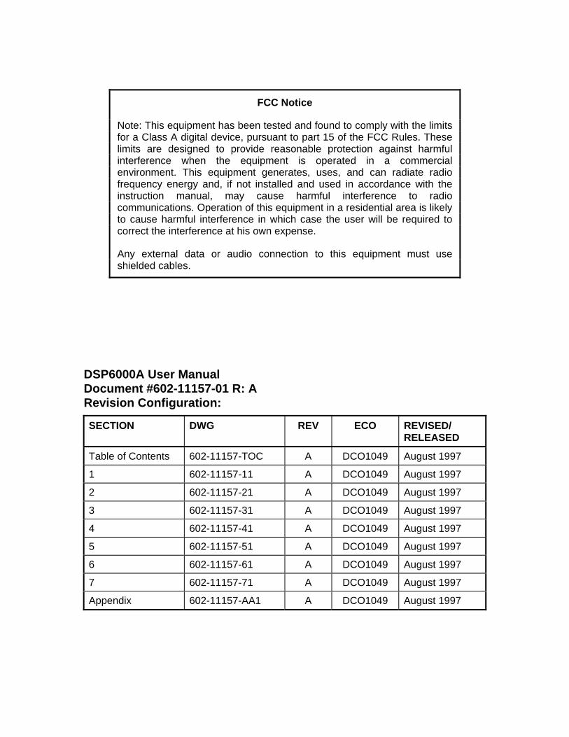
FCC Notice
Note: This equipment has been tested and found to comply with the limits for a Class A digital device, pursuant to part 15 of the FCC Rules. These limits are designed to provide reasonable protection against harmful interference when the equipment is operated in a commercial environment. This equipment generates, uses, and can radiate radio frequency energy and, if not installed and used in accordance with the instruction manual, may cause harmful interference to radio communications. Operation of this equipment in a residential area is likely to cause harmful interference in which case the user will be required to correct the interference at his own expense.
Any external data or audio connection to this equipment must use shielded cables.
DSP6000A User Manual Document #602-11157-01 R: A Revision Configuration:
SECTION DWG REV ECO REVISED/ RELEASED
Table of Contents 602-11157-TOC A DCO1049 August 1997
1 602-11157-11 A DCO1049 August 1997
2 602-11157-21 A DCO1049 August 1997
3 602-11157-31 A DCO1049 August 1997
4 602-11157-41 A DCO1049 August 1997
5 602-11157-51 A DCO1049 August 1997
6 602-11157-61 A DCO1049 August 1997
7 602-11157-71 A DCO1049 August 1997
Appendix 602-11157-AA1 A DCO1049 August 1997

DSP6000A 602-11157-11 R: A
Section 1
System Characteristics
Section Contents Page
1.1 Introduction 1-2 1.2 System Features 1-3 1.3 DSP6000A System 1-4 1.3.1 DSP6000A System Specifications 1-4 1.3.2 DSP6000E Encoder Specifications 1-5 1.3.3 DSP6000D Decoder Specifications 1-6 1.4 System Description 1-7 1.4.1 DSP6000E Encoder Description 1-7 1.4.2 DSP6000D Decoder Description 1-11
System Characteristics 1-6
DSP6000A 602-11157-11 R: A
1.1 Introduction
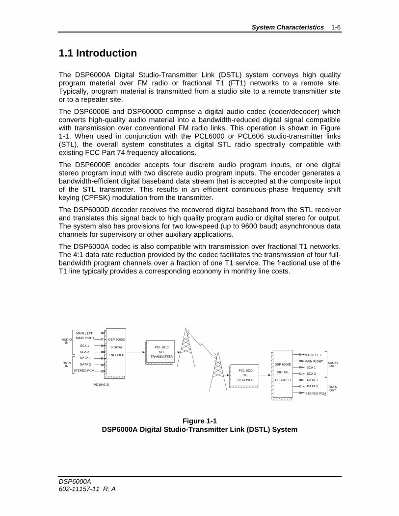
The DSP6000A Digital Studio-Transmitter Link (DSTL) system conveys high quality program material over FM radio or fractional T1 (FT1) networks to a remote site. Typically, program material is transmitted from a studio site to a remote transmitter site or to a repeater site.
The DSP6000E and DSP6000D comprise a digital audio codec (coder/decoder) which converts high-quality audio material into a bandwidth-reduced digital signal compatible with transmission over conventional FM radio links. This operation is shown in Figure 1-1. When used in conjunction with the PCL6000 or PCL606 studio-transmitter links (STL), the overall system constitutes a digital STL radio spectrally compatible with existing FCC Part 74 frequency allocations.
The DSP6000E encoder accepts four discrete audio program inputs, or one digital stereo program input with two discrete audio program inputs. The encoder generates a bandwidth-efficient digital baseband data stream that is accepted at the composite input of the STL transmitter. This results in an efficient continuous-phase frequency shift keying (CPFSK) modulation from the transmitter.
The DSP6000D decoder receives the recovered digital baseband from the STL receiver and translates this signal back to high quality program audio or digital stereo for output. The system also has provisions for two low-speed (up to 9600 baud) asynchronous data channels for supervisory or other auxiliary applications.
The DSP6000A codec is also compatible with transmission over fractional T1 networks. The 4:1 data rate reduction provided by the codec facilitates the transmission of four full-bandwidth program channels over a fraction of one T1 service. The fractional use of the T1 line typically provides a corresponding economy in monthly line costs.
(MD1049-2)
PCL 6010STL
TRANSMITTER
PCL 6020STL
AUDIOIN
DATAIN
MAIN LEFTMAIN RIGHT
SCA 1
SCA 2
DATA 1
DATA 2
STEREO PCM
DSP 6000E
DIGITAL
ENCODER
RECEIVER
AUDIOOUT
DATAOUT
MAIN LEFT
MAIN RIGHT
SCA 1
SCA 2
DATA 1
DATA 2
STEREO PCM
DSP 6000D
DIGITAL
DECODER
Figure 1-1 DSP6000A Digital Studio-Transmitter Link (DSTL) System
System Characteristics 1-7
DSP6000A 602-11157-11 R: A
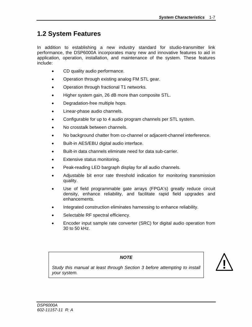
1.2 System Features
In addition to establishing a new industry standard for studio-transmitter link performance, the DSP6000A incorporates many new and innovative features to aid in application, operation, installation, and maintenance of the system. These features include:
• CD quality audio performance.
• Operation through existing analog FM STL gear.
• Operation through fractional T1 networks.
• Higher system gain, 26 dB more than composite STL.
• Degradation-free multiple hops.
• Linear-phase audio channels.
• Configurable for up to 4 audio program channels per STL system.
• No crosstalk between channels.
• No background chatter from co-channel or adjacent-channel interference.
• Built-in AES/EBU digital audio interface.
• Built-in data channels eliminate need for data sub-carrier.
• Extensive status monitoring.
• Peak-reading LED bargraph display for all audio channels.
• Adjustable bit error rate threshold indication for monitoring transmission quality.
• Use of field programmable gate arrays (FPGA’s) greatly reduce circuit density, enhance reliability, and facilitate rapid field upgrades and enhancements.
• Integrated construction eliminates harnessing to enhance reliability.
• Selectable RF spectral efficiency.
• Encoder input sample rate converter (SRC) for digital audio operation from 30 to 50 kHz.
NOTE
Study this manual at least through Section 3 before attempting to install your system.
!
System Characteristics 1-8
DSP6000A 602-11157-11 R: A
1.3 DSP6000A System
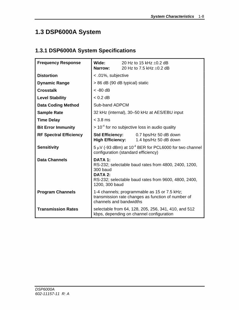
1.3.1 DSP6000A System Specifications
Frequency Response Wide: 20 Hz to 15 kHz ±0.2 dB Narrow: 20 Hz to 7.5 kHz ±0.2 dB
Distortion < .01%, subjective
Dynamic Range > 86 dB (90 dB typical) static
Crosstalk < -80 dB
Level Stability < 0.2 dB
Data Coding Method Sub-band ADPCM
Sample Rate 32 kHz (internal), 30–50 kHz at AES/EBU input
Time Delay < 3.8 ms
Bit Error Immunity > 10-4 for no subjective loss in audio quality
RF Spectral Efficiency Std Efficiency: 0.7 bps/Hz 50 dB down High Efficiency: 1.4 bps/Hz 50 dB down
Sensitivity 5 μV (-93 dBm) at 10-4 BER for PCL6000 for two channel configuration (standard efficiency)
Data Channels DATA 1: RS-232; selectable baud rates from 4800, 2400, 1200, 300 baud DATA 2: RS-232; selectable baud rates from 9600, 4800, 2400, 1200, 300 baud
Program Channels 1-4 channels; programmable as 15 or 7.5 kHz; transmission rate changes as function of number of channels and bandwidths
Transmission Rates selectable from 64, 128, 205, 256, 341, 410, and 512 kbps, depending on channel configuration
System Characteristics 1-9
DSP6000A 602-11157-11 R: A
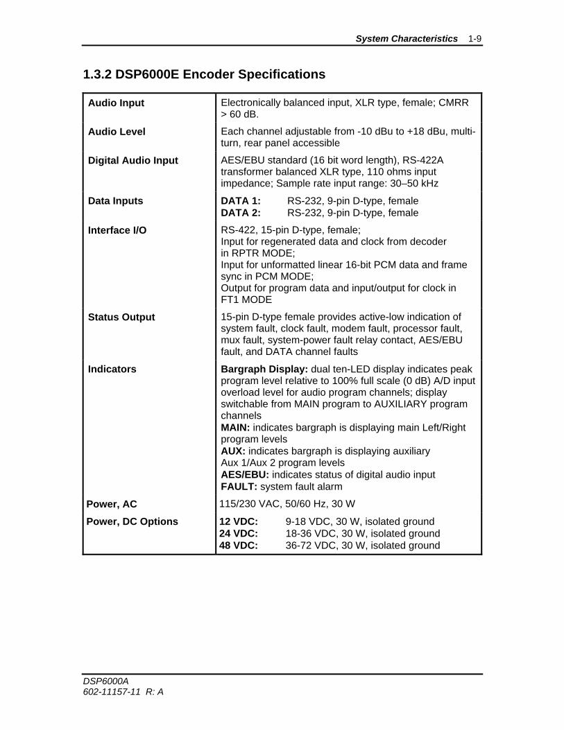
1.3.2 DSP6000E Encoder Specifications
Audio Input Electronically balanced input, XLR type, female; CMRR > 60 dB.
Audio Level Each channel adjustable from -10 dBu to +18 dBu, multi-turn, rear panel accessible
Digital Audio Input AES/EBU standard (16 bit word length), RS-422A transformer balanced XLR type, 110 ohms input impedance; Sample rate input range: 30–50 kHz
Data Inputs DATA 1: RS-232, 9-pin D-type, female DATA 2: RS-232, 9-pin D-type, female
Interface I/O RS-422, 15-pin D-type, female; Input for regenerated data and clock from decoder in RPTR MODE; Input for unformatted linear 16-bit PCM data and frame sync in PCM MODE; Output for program data and input/output for clock in FT1 MODE
Status Output 15-pin D-type female provides active-low indication of system fault, clock fault, modem fault, processor fault, mux fault, system-power fault relay contact, AES/EBU fault, and DATA channel faults
Indicators Bargraph Display: dual ten-LED display indicates peak program level relative to 100% full scale (0 dB) A/D input overload level for audio program channels; display switchable from MAIN program to AUXILIARY program channels MAIN: indicates bargraph is displaying main Left/Right program levels AUX: indicates bargraph is displaying auxiliary Aux 1/Aux 2 program levels AES/EBU: indicates status of digital audio input FAULT: system fault alarm
Power, AC 115/230 VAC, 50/60 Hz, 30 W
Power, DC Options 12 VDC: 9-18 VDC, 30 W, isolated ground 24 VDC: 18-36 VDC, 30 W, isolated ground 48 VDC: 36-72 VDC, 30 W, isolated ground
System Characteristics 1-10
DSP6000A 602-11157-11 R: A
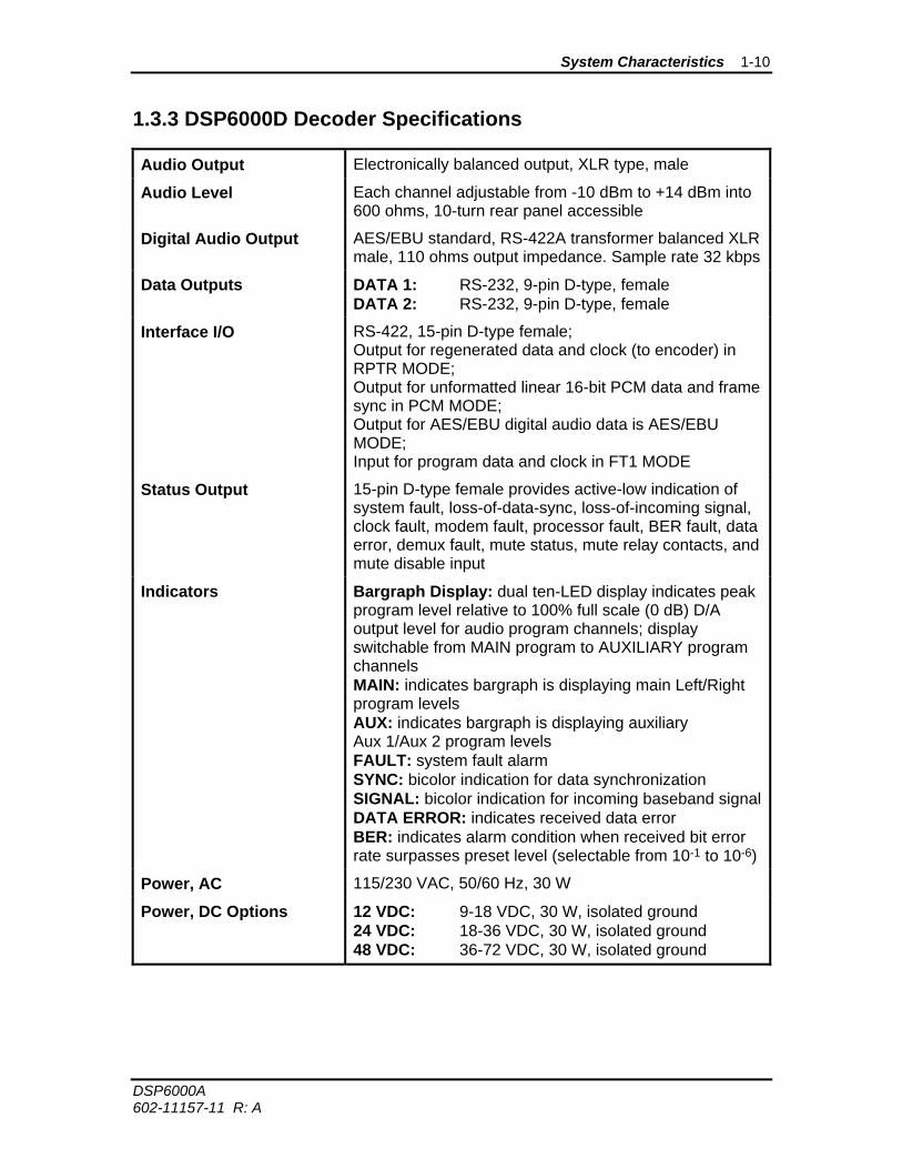
1.3.3 DSP6000D Decoder Specifications
Audio Output Electronically balanced output, XLR type, male
Audio Level Each channel adjustable from -10 dBm to +14 dBm into 600 ohms, 10-turn rear panel accessible
Digital Audio Output AES/EBU standard, RS-422A transformer balanced XLR male, 110 ohms output impedance. Sample rate 32 kbps
Data Outputs DATA 1: RS-232, 9-pin D-type, female DATA 2: RS-232, 9-pin D-type, female
Interface I/O RS-422, 15-pin D-type female; Output for regenerated data and clock (to encoder) in RPTR MODE; Output for unformatted linear 16-bit PCM data and frame sync in PCM MODE; Output for AES/EBU digital audio data is AES/EBU MODE; Input for program data and clock in FT1 MODE
Status Output 15-pin D-type female provides active-low indication of system fault, loss-of-data-sync, loss-of-incoming signal, clock fault, modem fault, processor fault, BER fault, data error, demux fault, mute status, mute relay contacts, and mute disable input
Indicators Bargraph Display: dual ten-LED display indicates peak program level relative to 100% full scale (0 dB) D/A output level for audio program channels; display switchable from MAIN program to AUXILIARY program channels MAIN: indicates bargraph is displaying main Left/Right program levels AUX: indicates bargraph is displaying auxiliary Aux 1/Aux 2 program levels FAULT: system fault alarm SYNC: bicolor indication for data synchronization SIGNAL: bicolor indication for incoming baseband signalDATA ERROR: indicates received data error BER: indicates alarm condition when received bit error rate surpasses preset level (selectable from 10-1 to 10-6)
Power, AC 115/230 VAC, 50/60 Hz, 30 W
Power, DC Options 12 VDC: 9-18 VDC, 30 W, isolated ground 24 VDC: 18-36 VDC, 30 W, isolated ground 48 VDC: 36-72 VDC, 30 W, isolated ground
System Characteristics 1-11
DSP6000A 602-11157-11 R: A
1.4 System Description
1.4.1 DSP6000E Encoder Description
The DSP6000E is a digital audio encoder designed to work with existing STL transmission equipment or fractional T1 telco lines. The system accepts four discrete audio inputs, a digital audio input, and two low-rate data inputs for encoding. The audio channels are converted to digital binary form. Digital signal processing then reduces each channel data rate by a factor of four. Channel data is multiplexed together with the data channels. This composite signal is available for output to a T1 CSU for fractional T1 transmission. Otherwise, the composite digital signal is processed by an efficient channel coding scheme. This signal is then output to frequency modulate any FM-type STL transmitter.
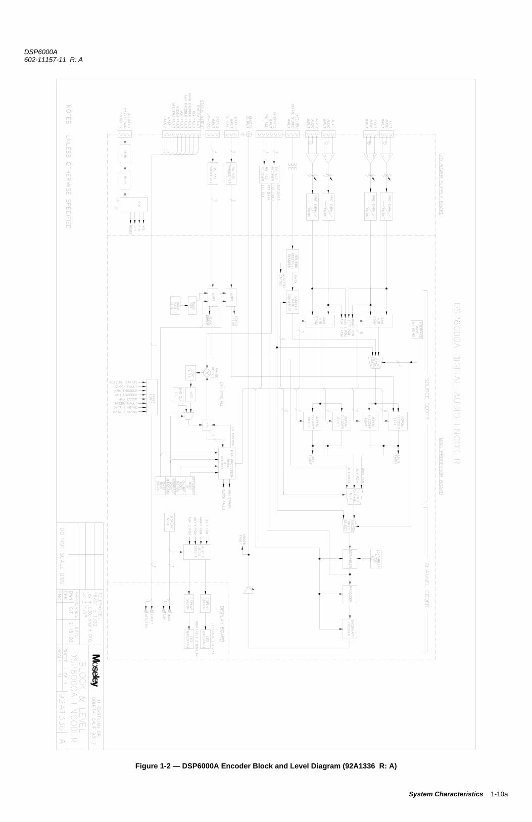
The encoder is physically partitioned into three printed circuit assemblies—the I/O board, the main processor board, and the display board. Functionally, the encoder is partitioned into six groups which are described below. Refer to Figure 1-2, Encoder Block and Level Diagram, for reference to this section.
Audio-Digital I/O Interface (I/O Board)
The audio-digital I/O interface consists of four active balanced program audio inputs (LEFT, RIGHT, AUX 1, and AUX 2) with input level adjustments and selectable active preemphasis, AES/EBU digital stereo input (MAIN only), RS-232 data inputs, RS-422 INTERFACE input, and buffered STATUS output. This board provides the appropriate signal conditioning, I/O buffering, and electromagnetic interference (EMI) protection between the outside world and the main processor portion of the encoder.
Source Encoder (Main Processor Board)
The source encoder converts the audio information into digital binary 1's and 0's serial format. The source encoder consists of the analog-to-digital (A/D) converters, the adaptive-differential pulse code modulation (ADPCM) encoders, and the data multiplexer. The A/D converters receive discrete audio inputs from the I/O board which are converted to 16-bit linear PCM serial data. The ADPCM encoders, in turn, convert these signals to 4-bit serial data, yielding a 4:1 data reduction. Alternatively, the main channel analog audio inputs (LEFT and RIGHT) may be replaced by one digital stereo audio input in AES/EBU format. In this case the main A/D converter is bypassed and the digital audio is input directly into the ADPCM encoder for data reduction.
The serial outputs from the ADPCM encoders (one from each channel), along with two low-rate asynchronous data channels, are then time division multiplexed together into one composite serial data stream. This data is available for output for T1 transmission or sent to the channel encoder for processing prior to channel transmission. System and data timing are derived internally from a crystal clock reference for STL operation, or are derived either internally or externally for fractional T1 synchronization.
System Characteristics 1-12
DSP6000A 602-11157-11 R: A
Channel Encoder (Main Processor Board)
The channel encoder processes the serial binary data from the source encoder into a multilevel, spectrally shaped signal prior to channel transmission. The channel encoder consists of the scrambler, precoder, and shaping filter. The scrambler eliminates discrete spectral information. The precoder eliminates error propogation. The shaping filter produces either a 3-level or 7-level shaped data signal that corresponds to “standard” or “high” spectral efficiency transmission modes, respectively.
The channel encoder also accepts data from the external INTERFACE input, bypassing the internal source encoder, to facilitate repeater operation or the use of alternate source coding equipment. For FT1 operation the channel encoder is bypassed and only the source encoder is used.
Timing and Control (Main Processor Board)
The channel configuration (1 to 4 audio channels with 1 or 2 data channels), the channel bandwidths (15 kHz or 7.5 kHz), and resulting data transmission rate (64 kbps to 512 kbps) are determined through the mode selection DIP switches M0 to M3. The interface mode DIP switches M4, M5, and M6 select I/O source data from the following: 1) internal program channels with internal synchronization for standard STL/FT1 operation, 2) internal program channels with external synchronization for FT1 operation, 3) external program data for repeater operation or outboard source coding, 4) AES/EBU digital audio input, or 5) unformatted linear PCM input. RF spectral efficiency is selected between “standard” (3-level) and “high” (7-level) with DIP switch D1.
Status and Metering (Display Board)
This board contains the front panel indicator LED’s. The peak program level of the discrete audio channels is displayed in MAIN or AUX channel pairs on the dual LED bargraphs. A tricolor LED displays the status and condition of the AES/EBU digital audio input. A red LED gives indication of system failure.
Power Supply (I/O Board)
The power supply converts AC line source (115 VAC or 230 VAC, internally wired) to three regulated voltages: +5 VDC, +15 VDC, and -15 VDC. Supervisory functions provide system reset for power-up and low voltage conditions (for example, power drop out or brown out) and crowbar/pull-down on the +5 VDC line during overvoltage conditions (for example, from a faulty regulator) to protect vital processing components.
Note
Once the crowbar is tripped the system may require a new fuse or manually removing and reapplying AC power to bring the system up.
System Characteristics 1-13
DSP6000A 602-11157-11 R: A
DC Option
The DC option uses a triple output DC-DC converter with a 12, 24, or 48V input. The linear regulators are bypassed on the I/O card. The inputs are isolated, allowing for positive or negative ground operation.
System Characteristics 1-14
DSP6000A 602-11157-11 R: A
This page is intentionally blank.
DSP6000A 602-11157-11 R: A
System Characteristics 1-10a
Figure 1-2 — DSP6000A Encoder Block and Level Diagram (92A1336 R: A)
System Characteristics 1-11
DSP6000A 602-11157-11 R: A
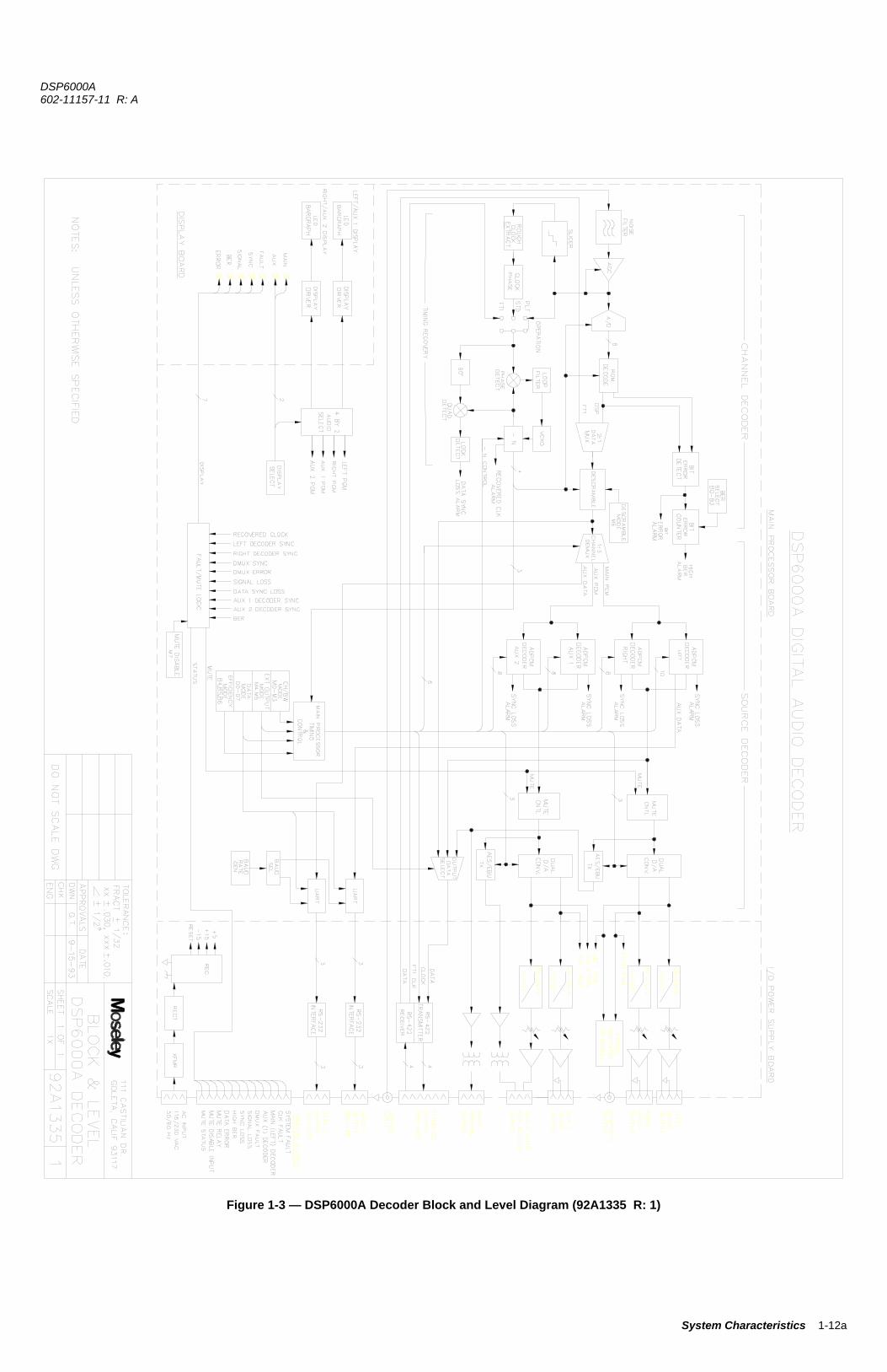
1.4.2 DSP6000D Decoder Description
The DSP6000D is a digital audio decoder designed to work through existing STL receiving equipment or fractional T1 telco lines. The decoder accepts the recovered baseband signal at the STL receiver demodulator output which had originally been generated by the companion DSP6000E encoder and STL transmitter. From the STL baseband signal the decoder recovers the encoded data and associated data timing. For FT1 operation where an STL is not required the decoder accepts RS-422 data and timing directly. The data is demultiplexed into the original data subgroups, which are in turn converted back into discrete audio, formatted digital audio, and data channels.
The decoder is physically partitioned into three printed circuit boards—the I/O board, the main processor board, and the display board. Functionally, the decoder is partitioned into six groups which are described below. Refer to Figure 1-3, Decoder Block and Level Diagram, for reference to this section.
Audio-Digital I/O Interface (I/O Board)
The audio-digital I/O interface consists of four program audio active balanced outputs (LEFT, RIGHT, AUX 1, and AUX 2) with output level adjustments and selectable active de-emphasis, AES/EBU digital stereo outputs (both MAIN and AUX), RS-232 data outputs, RS-422 INTERFACE output, and buffered STATUS output. This board provides the appropriate signal conditioning, I/O buffering, and electromagnetic interference (EMI) protection between outside world and the main processor portion of the decoder.
Channel Decoder (Main Processor Board)
The channel decoder converts the encoded multilevel baseband signal from the STL receiver demodulator into the binary data stream that was originally generated at the input of the channel encoder portion of the DSP6000E encoder. The channel decoder consists of an active low-pass Bessel noise filter, automatic gain control, analog-to-digital convertor, ROM decoder, timing recovery phase-locked loop, data descrambler, data error detection, and BER (bit error rate) flag. The regenerated data stream is routed to the source decoder and to the external INTERFACE output port. The external output facilitates repeater operation or the use of alternate source decoding equipment. The channel decoder is bypassed for FT1 operation.
Source Decoder (Main Processor Board)
The source decoder performs the inverse operation of the source encoder of the DSP6000E, converting the serial bit stream back into audio and data channels. The source decoder consists of the demultiplexer, the ADPCM decoders, and the digital-to-analog (D/A) converters. The data stream from the channel decoder is demultiplexed into the original channel data streams. The ADPCM decoders convert serial 4-bit words into linear 16-bit PCM data. The PCM data is converted to formatted AES/EBU digital audio data for digital output, or to discrete audio by the D/A converters for analog output.
DSP6000A 602-11157-11 R: A
System Characteristics 1-10a
Timing and Control (Main Processor Board)
The channel configuration (1 to 4 audio channels with 1 or 2 data channels), the channel bandwidths (15 kHz or 7.5 kHz), and the resulting data transmission rate (64 kbps to 512 kbps) are determined through mode selection DIP switches M0 to M3. These settings will typically match that of the encoder for correct operation. Interface mode DIP switches M4, M5, and D1 configure data I/O at the INTERFACE port from the following: 1) program data output with internal synchronization for repeater operation or outboard source decoding, 2) program data output with external synchronization for FT1 operation, 3) AES/EBU digital audio output, or 4) raw PCM data output. RF spectral efficiency is selected between “standard” and “high” with DIP switch B4.
Status and Metering (Display Board)
This board contains the front panel indicator LED’s. The peak program output level of the discrete audio channels is displayed in MAIN or AUX channel pairs on the dual LED bargraphs. Two bicolor LED’s display signal and data-sync status. Two red LED’s give indication of system failure and BER threshold. A yellow LED indicates individual data errors.
Power Supply (I/O Board)
The power supply converts AC line source (115 VAC or 230 VAC, internally wired) to three regulated voltages: +5 VDC, +15 VDC, and -15 VDC. Supervisory functions provide system reset for power-up and low voltage conditions (for example, power drop out or brown out) and crowbar/pull-down on the +5 VDC line during overvoltage conditions (for example, from a faulty regulator) to protect vital processing components.
Note
Once the crowbar is tripped the system may require a new fuse or manually removing and reapplying AC power to bring the system up.
DC Option
The DC option uses a triple output DC-DC converter with a 12, 24, or 48V input. The +5V and -15V linear regulators are bypassed on the I/O card; the +15V linear regulator is not bypassed, in order to maintain tighter regulation for critical decoder components. The inputs are isolated, allowing for positive or negative ground operation.
DSP6000A 602-11157-11 R: A
System Characteristics 1-12a
Figure 1-3 — DSP6000A Decoder Block and Level Diagram (92A1335 R: 1)

DSP6000A 602-11157-21 R: A
Section 2
Installation
Section Contents Page
2.1 Unpacking 2-2 2.2 Power 2-2 2.2.1 AC Line Voltage Selection 2-2 2.2.2 DC Option Fuses 2-4 2.3 Pre-Installation Checkout 2-5 2.3.1 Checkout of Encoder/Decoder Only 2-5 2.3.2 Checkout of System — Encoder/STL/Decoder 2-7 2.4 Rack Installation 2-9 2.5 STL Installation 2-10 2.5.1 Encoder 2-10 2.5.2 Decoder 2-12 2.5.3 Air-Chain Processing 2-14 2.5.4 Repeater 2-16 2.6 Fractional T1 (FT1) Installation 2-18 2.7 Data Communications 2-22 2.7.1 Data Rate and Format Selection 2-22 2.7.2 Remote Control Communication 2-23 2.7.2.1 Subcarrier Communications 2-23 2.7.2.2 FSK Communications 2-23 2.7.2.3 RS-232 Communications 2-24 2.8 Retrofit STL Installation 2-31 2.8.1 PCL6010 Transmitter 2-31 2.8.2 PCL6020/6030/6060 Receiver 2-32 2.8.3 PCL606 Transmitter, Mono 2-36 2.8.4 PCL606 Receiver, Mono 2-38 2.8.5 PCL606/C Transmitter, Composite 2-40 2.8.6 PCL606/C Receiver, Composite 2-41 2.8.7 PCL505 Transmitter, Composite 2-43 2.8.8 PCL505 Receiver, Composite 2-44 2.8.9 Other Radios 2-45 2.8.10 Retrofit Repeater Installation with STL 2-46
Installation 2-16
DSP6000A 602-11157-21 R: A
2.1 Unpacking
The DSP6000A Encoder and Decoder should be carefully unpacked and inspected for shipping damage. Should inspection reveal any shipping damage, visible or hidden, immediately file a claim with the carrier. Keep all packing materials at least until correct performance of the system is confirmed. If possible, save all packing materials in case the unit must be shipped in the future.
Units configured to order by the factory may be accompanied by additional components in the shipping container. These may not be required for the intended application, but should be retained for future reconfiguration.
We recommend removal of the top covers of both the encoder and decoder for a brief inspection of the internal components. Verify that assemblies and cables are mechanically secure. Check also for socketed components that may have been jarred loose or partially dismounted. This is a good time to familiarize yourself with the various assemblies, using the Block and Level diagrams (Figures 1-2 and 1-3) and the drawings of Section 7. After the internal inspection, replace the top covers or continue directly to Section 2.2.
CAUTION
Do not make adjustments of any kind until the nature of each adjustment is understood.
Do not apply AC power to the encoder or decoder until the procedure in Section 2.2.1 is completed.
2.2 Power
The encoder and decoder are each capable of operating at one of the two nominal AC power source voltages of 115 or 230 VAC, 50–60 Hz. Optionally, one or both units may configured for 12, 24, or 48 VDC operation. Units are configured for 115 VAC operation when shipped, unless otherwise specified. See Section 2.2.1 for AC operation or Section 2.2.2 for DC operation.
2.2.1 AC Line Voltage Selection
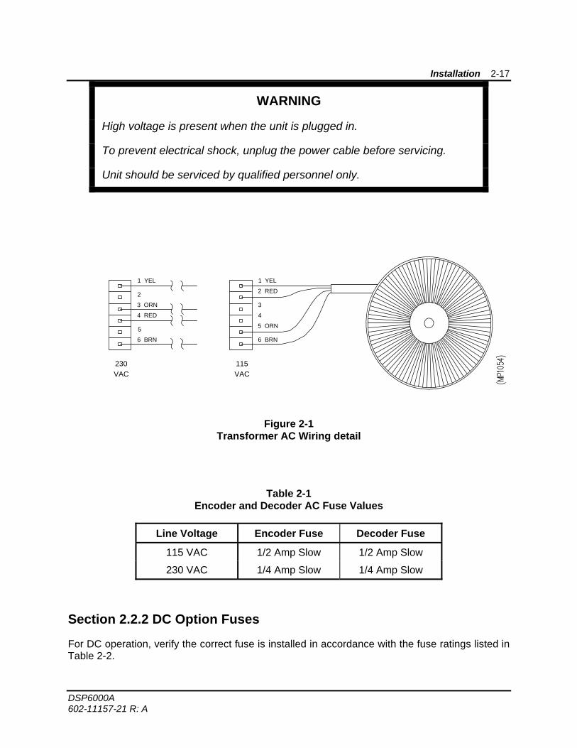
The AC operating voltage is determined by the wiring of the power transformer inside the unit. To change the operating voltage configuration, rewire the transformer connector as shown in Figure 2-1. The electrical contacts can be extracted from the insulating connector shell by using a pointed tool to depress the detents, which are accessible through the side of the shell. Insert each contact into its new location until it is secured by the detent. Tug gently to verify the contact is correctly installed. If the operating voltage is changed, change the fuse also in accordance with the fuse ratings listed in Table 2-1 (also found on the rear panel of each unit).
Installation 2-17
DSP6000A 602-11157-21 R: A
WARNING
High voltage is present when the unit is plugged in.
To prevent electrical shock, unplug the power cable before servicing.
Unit should be serviced by qualified personnel only.
1 YEL
2
3 ORN
4 RED
5
6 BRN
230VAC
115VAC
1 YEL
2 RED
3
4
5 ORN
6 BRN
Figure 2-1 Transformer AC Wiring detail
Table 2-1 Encoder and Decoder AC Fuse Values
Line Voltage Encoder Fuse Decoder Fuse
115 VAC 1/2 Amp Slow 1/2 Amp Slow
230 VAC 1/4 Amp Slow 1/4 Amp Slow
Section 2.2.2 DC Option Fuses
For DC operation, verify the correct fuse is installed in accordance with the fuse ratings listed in Table 2-2.
Installation 2-18
DSP6000A 602-11157-21 R: A
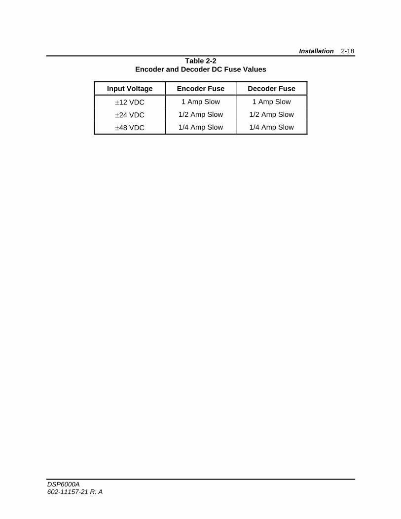
Table 2-2 Encoder and Decoder DC Fuse Values
Input Voltage Encoder Fuse Decoder Fuse
±12 VDC 1 Amp Slow 1 Amp Slow
±24 VDC 1/2 Amp Slow 1/2 Amp Slow
±48 VDC 1/4 Amp Slow 1/4 Amp Slow
Installation 2-19
DSP6000A 602-11157-21 R: A
2.3 Pre-Installation Checkout
While both encoder and decoder are at the same location, we suggest that a checkout of the system be performed before mounting the equipment in racks separated by many miles. This also allows for verification of fault conditions and mode selection, which will be discussed in subsequent sections.
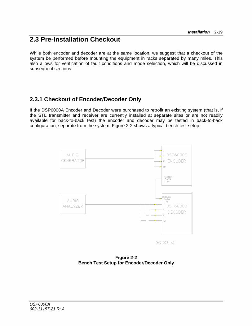
2.3.1 Checkout of Encoder/Decoder Only
If the DSP6000A Encoder and Decoder were purchased to retrofit an existing system (that is, if the STL transmitter and receiver are currently installed at separate sites or are not readily available for back-to-back test) the encoder and decoder may be tested in back-to-back configuration, separate from the system. Figure 2-2 shows a typical bench test setup.
Figure 2-2 Bench Test Setup for Encoder/Decoder Only
Installation 2-20
DSP6000A 602-11157-21 R: A
Test Equipment
Audio signal generator and analyzer (HP 339 or equivalent)
Procedure
1. Connect the system as shown in Figure 2-2 and apply AC power to the encoder and decoder. The presence of power is indicated by the green display mode LED's, MAIN or AUX, on both encoder and decoder.
On the encoder, the red FAULT LED and the bicolor AES/EBU LED should both be off.
On the decoder, the bicolor status LED's SIGNAL and SYNC should display green, while the red status LED's FAULT and BER, and the yellow status LED DATA ERROR should be all off within a few seconds after power-up.
2. Remove the signal from DECODE DATA IN on the decoder.
SIGNAL, SYNC, and FAULT should turn red and BER and DATA ERROR should turn on. Reconnect the signal to DECODE DATA IN.
3. Apply audio to the encoder audio input at +10 dBu. The display mode should be set to the appropriate channel, MAIN or AUX, for both encoder and decoder.
The encoder LED bar graph should be registering to the yellow (-3 dB) level.
The decoder LED bargraph should also register to the yellow (-3 dB) level, and the decoder output level should be approximately +10 dBm (600 ohms).
4. The input signal may be removed and the audio signal-to-noise ratio (SNR) measured using a 22 kHz measurement bandwidth.
Installation 2-21
DSP6000A 602-11157-21 R: A
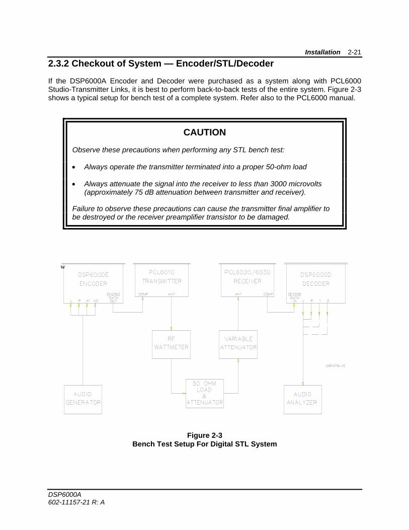
2.3.2 Checkout of System — Encoder/STL/Decoder
If the DSP6000A Encoder and Decoder were purchased as a system along with PCL6000 Studio-Transmitter Links, it is best to perform back-to-back tests of the entire system. Figure 2-3 shows a typical setup for bench test of a complete system. Refer also to the PCL6000 manual.
CAUTION
Observe these precautions when performing any STL bench test:
• Always operate the transmitter terminated into a proper 50-ohm load
• Always attenuate the signal into the receiver to less than 3000 microvolts (approximately 75 dB attenuation between transmitter and receiver).
Failure to observe these precautions can cause the transmitter final amplifier to be destroyed or the receiver preamplifier transistor to be damaged.
w
Figure 2-3 Bench Test Setup For Digital STL System
Installation 2-22
DSP6000A 602-11157-21 R: A
Test Equipment
RF wattmeter with measurement range of 5–12 watts (Bird 43 or equivalent)
50 ohm, 10 watt dummy load for 950 MHz with 30 dB of attenuation output capability (Sierra 661A-30 or equivalent)
Variable attenuator, 0–100 dB at 950 MHz (Kay Model 432D or equivalent)
Audio distortion analyzer (HP 339 or equivalent)
Procedure
1. With the wattmeter and dummy load connected to the transmitter, apply AC power to the receiver. The SIGNAL LED will be red, indicating that there is no RF.
2. Apply AC power to the transmitter and place the OPERATE/STANDBY switch in the OPERATE position. The RADIATE and AFC LED's will change from red to green. Observe that the wattmeter indicates 5–8 watts and that the transmitter meter will provide readings of FWD POWER.
A brief period after the RADIATE LED turns green, the SIGNAL LED on the receiver should change from red to green. The RF LEVEL meter position on the receiver may be selected to determine the strength of the RF signal received.
3. Adjust the variable attenuator until an input signal strength of approximately 1000 microvolts is indicated. It should be noted that, in any bench test where the transmitter and receiver are in close proximity, there can be sufficient RF leakage from the cables to render impractical any computations of applied signal strength based upon power and attenuation data.
4. At this point, the encoder/decoder portion of the system may be tested as described in the prior section (that is, for encoder/decoder only).
5. This is also a good opportunity to verify threshold performance of the system. Increase the variable attenuation until the decoder DATA ERROR status LED begins to flicker. The STL receiver signal strength should be on the order of 5 μV–10 μV, depending on the system configuration.
As the attenuation is increased, the decoder BER (Bit Error Rate) red LED will eventually illuminate. This indicates an error rate in excess of 10-2 (1 error in 100 bits of data). There will also be an audible click from the MUTE relay. This error rate is factory set but is internally selectable for other rates (see Section 5). Due to the nature of digital transmission, the system will transition from error-free operation to failure in only 2–4 dB of attenuation once the error threshold is reached.
This concludes the basic bench test of the units. The user may want to run further experiments to become familiar with the system. Before proceeding with higher level testing, consult Sections 1–3 for a thorough understanding of the DSP6000A system.
Installation 2-23
DSP6000A 602-11157-21 R: A
2.4 Rack Installation
NOTE
Always pre-test the system on the bench in its intended configuration prior to installation at a remote site.
The DSP6000A Encoder and Decoder are designed for mounting in standard rack cabinets, preferably between waist and shoulder height. The encoder and decoder have mounting holes for Chassis Trak C-300-5-1-14 chassis rack slides. If the rack will accept chassis rack slides, their use is recommended. When using rack slides, be sure to leave at least a 15-inch service loop in all cables to the equipment.
When mounted in a rack, the unit must have an unobstructed free flow of cooling air above and, if possible, below the unit. Continued operation in a confined environment can cause the ambient temperature to exceed specification, resulting in reduced life or system failure.
It is desirable to collocate the encoder with the STL transmitter to reduce the length of the interconnect cable. Similarly, the decoder should be located with the STL receiver. Due to strong electromagnetic interference (EMI) typical at a transmitter site, RF field conduction on long interconnect cables can adversely effect the system error performance and cause audio drop-outs.
NOTE
Avoid cable interconnection length in excess of 1 meter in strong RF environments.
We highly recommend installation of lightning protectors in the power lines to the encoder and decoder to prevent line surges from damaging expensive components.
In configurations of two STL transmitters with the DSP6000E Encoder, Moseley’s TPT-2 transfer panel may be installed to provide automatic switchover upon detectable transmitter failure. The transmitters should not already incorporate automatic transfer. Mount the transfer panel between the transmitters, thereby allowing short cables and better ventilation.
For automatic switchover in systems using the DSP6000D Decoder with two STL receivers, install the MOSELEY TPR-2 transfer panel. The receivers should not already incorporate automatic transfer, and the TPR-2 should be mounted between them.
Installation 2-24
DSP6000A 602-11157-21 R: A
2.5 STL Installation
2.5.1 Encoder
Encoder/STL Connection
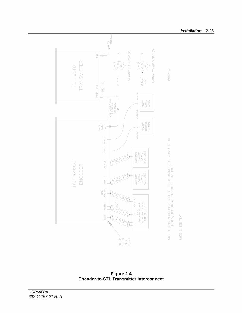
Figure 2-4 depicts a typical interconnection of a DSP6000E Encoder with a PCL6010 STL transmitter for normal operation. The interconnect cable between encoder ENCODE DATA OUT and STL transmitter COMPOSITE IN should be coaxial type (RG-58A/U or equivalent) with BNC male connectors on each end.
Encoder Audio Input Levels LEFT, RIGHT, AUX 1, and AUX 2 discrete audio program levels are displayed on the peak-reading LED bargraph on the front panel. The 0 dB/100% point refers to full-scale input of the encoder analog-to-digital (A/D) converters. Audio inputs above this level are clipped, which causes distortion and sounds bad! Allow some headroom when setting the input levels. Apply audio program and set the input level for meter readings to the -3 dB (yellow) LED on the largest program peaks (the corresponding VU reading will be approximately 4-14 dB below the peak audio level displayed by the meter, depending on the program source material). Ideally, some form of peak limiting or leveling should precede the encoder audio inputs.
NOTE
Do not allow the audio level to read into the red (0 dB) on the LED bargraph, as this causes severe distortion.
The AES/EBU input accepts digital stereo audio input in place of the LEFT/RIGHT discrete stereo input. This input requires no level adjustment. Unlike the main LEFT/RIGHT inputs, the AES/EBU input is not displayed on the LED bargraph. See Section 5 for AES/EBU selection.
Encoder DATA OUTPUT Level to STL The encoder output level and transmitter deviation are calibrated at the factory. Normally, no other adjustments are required. If the encoder is ordered separately from the STL transmitter, as an add-on or for retrofitting, then some minor STL modifications may be required. Refer to Section 2.8 (Retrofit STL Installation) for further details.
STL Transmitter MUX Input The STL MUX channel is usable only under certain circumstances when the STL is used for digital transmission. See Section 2.8.2 for MUX subcarrier configurations.
Installation 2-25
DSP6000A 602-11157-21 R: A
Figure 2-4 Encoder-to-STL Transmitter Interconnect
Installation 2-26
DSP6000A 602-11157-21 R: A
2.5.2 Decoder
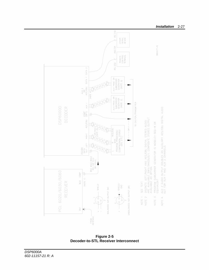
STL/Decoder Connection Figure 2-5 depicts a typical interconnection of DSP6000D Decoder and a PCL6020/6030/6060 STL receiver for normal operation. The interconnect cable between decoder DECODE DATA IN and STL receiver COMPOSITE OUT should be coaxial type RG-58A/U or equivalent with BNC male connectors on each end.
NOTE
In hostile or high-level RF environments we strongly recommend the use of double-shielded coaxial cable RG-142 or equivalent to insure proper decoder operation.
Decoder Output Levels LEFT, RIGHT, AUX 1, and AUX 2 discrete audio program levels are displayed on the peak-reading LED bargraph on the front panel. The 0 dB/100% point refers to full-scale output of the decoder digital-to-analog (D/A) converters. The outputs will not exceed this level (they are limited by the encoder A/D converters). With the audio level displaying full scale on the bargraph, the balanced audio XLR outputs may be adjusted between -10 dBm to +14 dBm into 600 ohm loads.
The AES/EBU output generates digital stereo audio simultaneously with the Left/Right discrete stereo output. This output is digital and requires no level adjustment. Unlike the encoder, AES/EBU audio levels are displayed on the LED bargraph on the decoder. AES/EBU output is also available for the AUX 1/AUX 2 channel pair by selecting jumpers at the AUX 2 XLR connector. For this output configuration, AUX 1 channel provides AUX 1 discrete audio with AUX AES/EBU digital output on AUX 2 channel.
Decoder DATA INPUT Level from STL The decoder input level and receiver output level are calibrated at the factory. No other adjustments are required. If the decoder is ordered separately from the DSTL system, as an add-on or for retrofitting, some minor STL modifications may be required. Refer to Section 2.8 Retrofit STL Installation for further details.
STL Receiver Multiplex Output The MUX channel is usable only under certain circumstances when the STL is used for digital transmission. See Section 2.8.2 for subcarrier MUX configurations.
Installation 2-27
DSP6000A 602-11157-21 R: A
Figure 2-5 Decoder-to-STL Receiver Interconnect
Installation 2-28
DSP6000A 602-11157-21 R: A
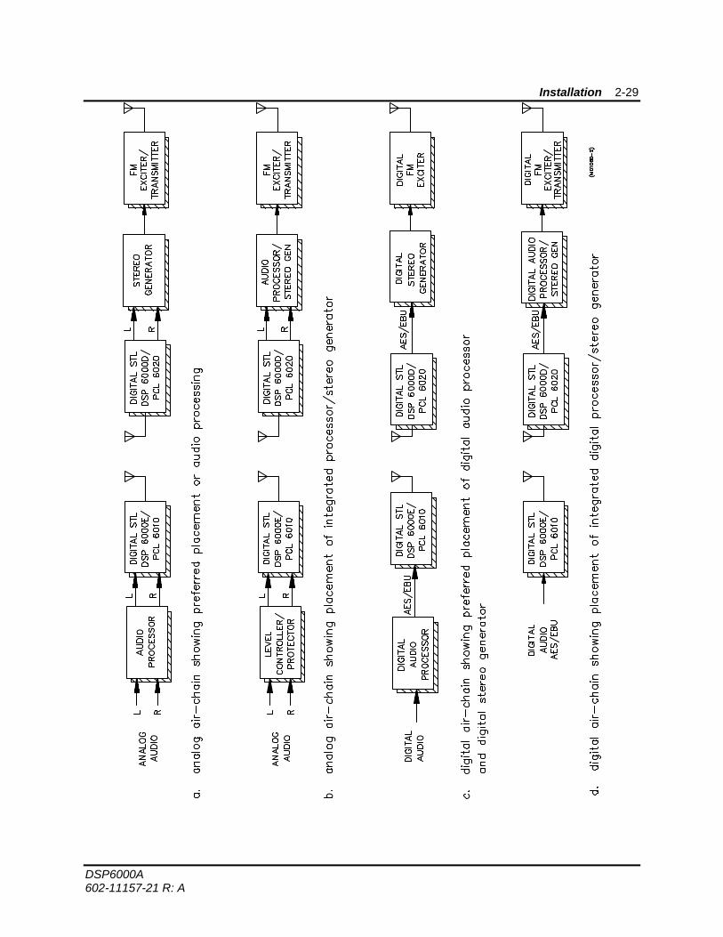
2.5.3 Air-Chain Processing
There are important considerations when installing or partitioning the audio processing around the digital studio-transmitter link:
• The DSP6000A system accepts and processes only discrete analog or digital audio. Systems requiring composite outputs must place the composite generator following the decoder output (an optional composite output is available for the decoder). This is analogous to the dual-mono STL configuration. Similarly, auxiliary SCA channels require the subcarrier generator to be placed after the decoder output.
• Do not use preemphasized audio in the encoder. Use flat audio only. Preemphasized audio will effect encoder source processing and unnecessarily reduce the available headroom. The DSP6000E encoder provides jumper-selectable de-emphasis to compensate for preemphasized discrete audio inputs that are provided by some audio processors.
• It is desirable to place all air-chain audio processing (equalization, compression, limiting) preceding the encoder. It may be possible for processing following the encoder to unmask artifacts from the source coding process. However, other factors of operational practicality may outweigh this consideration.
• Avoid multiple generations through devices that employ audio data reduction. This may unmask processing artifacts. The maximum number of passes through devices that incorporate the aptX-100 data reduction source processing used in the DSP6000A is about seven to eight times before discernible artifacts appear. The effect of combining audio data reduction schemes from different manufacturers are unpredictable and may reduce the number of generations for acceptable audio quality.
Figure 2-6 shows some examples of partitioning of air-chain audio processing. Figure 2-6a presents the preferred partitioning of the traditional analog audio processing chain. The digital STL should be placed between the audio processor and stereo generator. This extends the dynamic range of the STL and provides convenient studio access to the audio processor.
Many stations use the integrated processor/stereo generator. Typically, the composite output is transmitted though a composite STL. For a discrete STL, the composite generator must follow the STL and precede the FM exciter. Therefore, the integrated processor/stereo generator must be placed at the transmitter site, as in Figure 2-6b.
The preferred digital processing configuration is shown in Figure 2-6c. The DSP6000A facilitates the direct digital audio air-chain via AES/EBU digital audio inputs and outputs.
When using a fully digital integrated audio processor/stereo generator, the composite output must follow the discrete STL, which places audio processing at the transmitter site, as shown in Figure 2-6d. Many of these digital processors provide RS-232 control of their audio parameters. Therefore, studio control of the audio processor may be accomplished through phone lines or via the RS-232 data channel provided with the DSP6000A.
Installation 2-29
DSP6000A 602-11157-21 R: A
Installation 2-30
DSP6000A 602-11157-21 R: A
Figure 2-6 Air-Chain Processing with the Digital STL
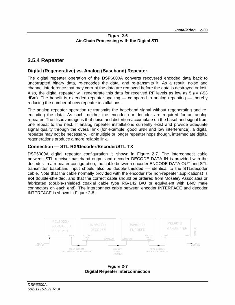
2.5.4 Repeater
Digital (Regenerative) vs. Analog (Baseband) Repeater The digital repeater operation of the DSP6000A converts recovered encoded data back to uncorrupted binary data, re-encodes the data, and re-transmits it. As a result, noise and channel interference that may corrupt the data are removed before the data is destroyed or lost. Also, the digital repeater will regenerate this data for received RF levels as low as 5 μV (-93 dBm). The benefit is extended repeater spacing — compared to analog repeating — thereby reducing the number of new repeater installations.
The analog repeater operation re-transmits the baseband signal without regenerating and re-encoding the data. As such, neither the encoder nor decoder are required for an analog repeater. The disadvantage is that noise and distortion accumulate on the baseband signal from one repeat to the next. If analog repeater installations currently exist and provide adequate signal quality through the overall link (for example, good SNR and low interference), a digital repeater may not be necessary. For multiple or longer repeater hops though, intermediate digital regenerations produce a more reliable link.
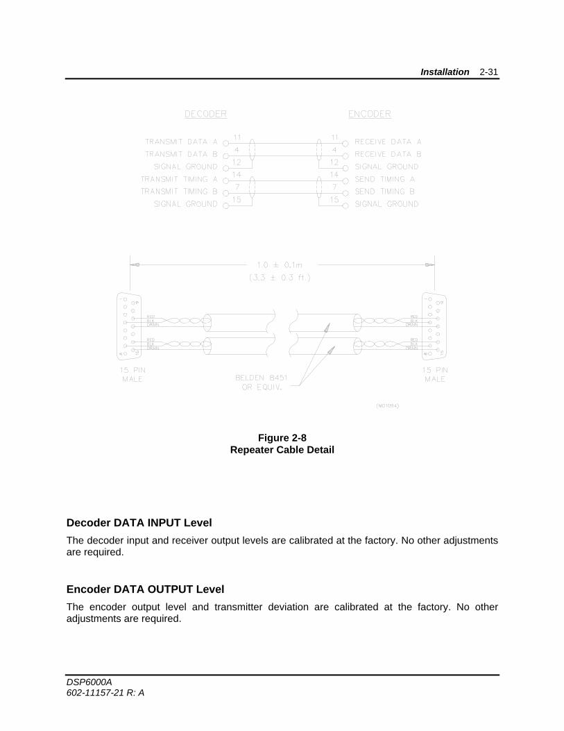
Connection — STL RX/Decoder/Encoder/STL TX DSP6000A digital repeater configuration is shown in Figure 2-7. The interconnect cable between STL receiver baseband output and decoder DECODE DATA IN is provided with the decoder. In a repeater configuration, the cable between encoder ENCODE DATA OUT and STL transmitter baseband input should also be double-shielded — identical to the STL/decoder cable. Note that the cable normally provided with the encoder (for non-repeater applications) is not double-shielded, and that the correct cable should be ordered from Moseley Associates or fabricated (double-shielded coaxial cable type RG-142 B/U or equivalent with BNC male connectors on each end). The interconnect cable between encoder INTERFACE and decoder INTERFACE is shown in Figure 2-8.
Figure 2-7 Digital Repeater Interconnection
Installation 2-31
DSP6000A 602-11157-21 R: A
Figure 2-8 Repeater Cable Detail
Decoder DATA INPUT Level The decoder input and receiver output levels are calibrated at the factory. No other adjustments are required.
Encoder DATA OUTPUT Level The encoder output level and transmitter deviation are calibrated at the factory. No other adjustments are required.
Installation 2-32
DSP6000A 602-11157-21 R: A
2.6 Fractional T1 (FT1) Installation
Fractional T1 T1 transmission service accommodates data rates up to 1.536 Mbps consisting of 24 time slots. Each time slot operates at 64 kbps. Fractional T1 service provides access to one or more of the 24 time slots. Typically, the use of the fractional T1 service will provide proportionally lower operating costs than that of a full (all 24 time slots) T1 service.
The DSP6000A system provides the ability to transmit and receive multiple high-quality audio channels through public or private T1 lines using the fractional capability of T1 service. A fractional T1 channel service unit (CSU) is required at both ends to provide an intelligent interface between the T1 network and the data terminal equipment (DTE) — that is, the DSP6000A codec. CSU’s are available from many manufacturers.
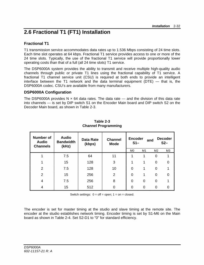
DSP6000A Configuration The DSP6000A provides N × 64 data rates. The data rate — and the division of this data rate into channels — is set by DIP switch S1 on the Encoder Main board and DIP switch S2 on the Decoder Main board, as shown in Table 2-3.
Table 2-3 Channel Programming
Number of Audio
Channels
Audio Bandwidth
(kHz)
Data Rate (kbps)
Channel Mode
Encoder S1–
and Decoder S2–
M0 M1 M2 M3
1 7.5 64 11 1 1 0 1
1 15 128 3 1 1 0 0
2 7.5 128 10 0 1 0 1
2 15 256 2 0 1 0 0
4 7.5 256 8 0 0 0 1
4 15 512 0 0 0 0 0
Switch settings: 0 = off = open; 1 = on = closed.
The encoder is set for master timing at the studio and slave timing at the remote site. The encoder at the studio establishes network timing. Encoder timing is set by S1-M6 on the Main board as shown in Table 2-4. Set S2-D1 to "0" for standard efficiency.
Installation 2-33
DSP6000A 602-11157-21 R: A
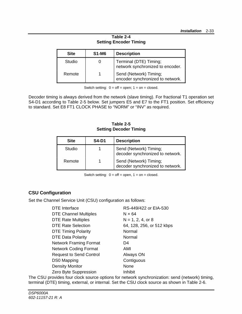
Table 2-4 Setting Encoder Timing
Site S1-M6 Description
Studio 0 Terminal (DTE) Timing; network synchronized to encoder.
Remote 1 Send (Network) Timing; encoder synchronized to network.
Switch setting: 0 = off = open; 1 = on = closed.
Decoder timing is always derived from the network (slave timing). For fractional T1 operation set S4-D1 according to Table 2-5 below. Set jumpers E5 and E7 to the FT1 position. Set efficiency to standard. Set E8 FT1 CLOCK PHASE to “NORM” or “INV” as required.
Table 2-5 Setting Decoder Timing
Site S4-D1 Description
Studio 1 Send (Network) Timing; decoder synchronized to network.
Remote 1 Send (Network) Timing; decoder synchronized to network.
Switch setting: 0 = off = open, 1 = on = closed.
CSU Configuration Set the Channel Service Unit (CSU) configuration as follows:
DTE Interface RS-449/422 or EIA-530 DTE Channel Multiples N × 64 DTE Rate Multiples N = 1, 2, 4, or 8 DTE Rate Selection 64, 128, 256, or 512 kbps DTE Timing Polarity Normal DTE Data Polarity Normal Network Framing Format D4 Network Coding Format AMI Request to Send Control Always ON DS0 Mapping Contiguous Density Monitor None Zero Byte Suppression Inhibit
The CSU provides four clock source options for network synchronization: send (network) timing, terminal (DTE) timing, external, or internal. Set the CSU clock source as shown in Table 2-6.
Installation 2-34
DSP6000A 602-11157-21 R: A
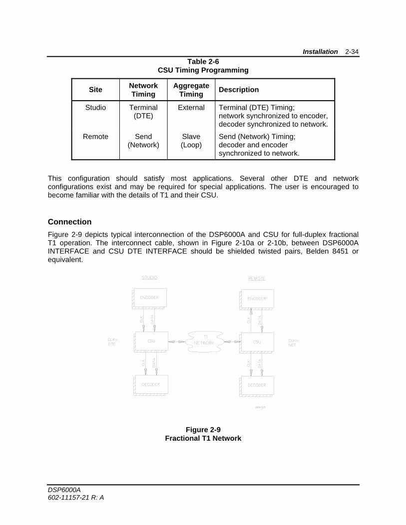
Table 2-6 CSU Timing Programming
Site Network Timing
Aggregate Timing Description
Studio Terminal (DTE)
External Terminal (DTE) Timing; network synchronized to encoder, decoder synchronized to network.
Remote Send (Network)
Slave (Loop)
Send (Network) Timing; decoder and encoder synchronized to network.
This configuration should satisfy most applications. Several other DTE and network configurations exist and may be required for special applications. The user is encouraged to become familiar with the details of T1 and their CSU.
Connection Figure 2-9 depicts typical interconnection of the DSP6000A and CSU for full-duplex fractional T1 operation. The interconnect cable, shown in Figure 2-10a or 2-10b, between DSP6000A INTERFACE and CSU DTE INTERFACE should be shielded twisted pairs, Belden 8451 or equivalent.
Figure 2-9 Fractional T1 Network
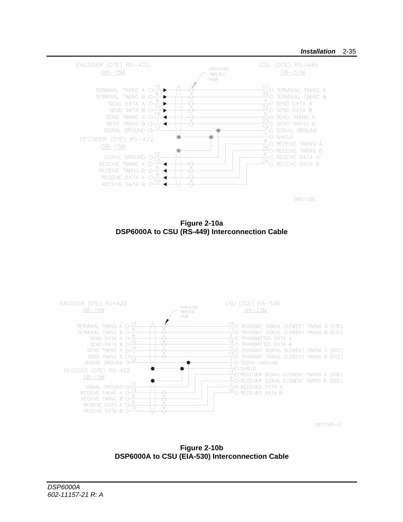
Installation 2-35
DSP6000A 602-11157-21 R: A
Figure 2-10a DSP6000A to CSU (RS-449) Interconnection Cable
Figure 2-10b DSP6000A to CSU (EIA-530) Interconnection Cable
Installation 2-36
DSP6000A 602-11157-21 R: A
2.7 Data Communications
In addition to audio transmission, the DSP6000A system provides data communication capability through RS-232 ports. This communication is unidirectional and provides data up-link for supervisory and remote control functions at the transmitter site.
2.7.1 Data Rate and Format Selection
Data channels DATA 1 and DATA 2 are asynchronous DCE ports capable of baud rates of 300, 1200, 2400, and 4800 baud. In addition, DATA 2 is capable of 9600 baud in some configurations. Factory default is 1200 baud. The data rates can be changed via DIP switches S5 and S6 on the decoder main board and switches S3 and S4 on the encoder main board. The data rates must be set at both the encoder and decoder. Be sure to select only one baud rate for each data channel. Refer to Section 5.9 for more information on data channel configuration.
Each data channel can be set for 8 or 7 data bits, and even, odd, or no parity. Each channel is fixed at 1 start and 1 stop bit. The factory default is 8 bits, no parity. The following tables summarize the data formats and their selection.
Table 2-7 DATA 1 Format
Encoder S2–
and Decoder S4– Data Bits Parity Total Bits
D2 D3 D4
0 0 0 8 None 10 (Default)
0 0 1 8 None 10
0 1 0 8 Even 11
0 1 1 8 Odd 11
1 0 0 7 None 9
1 0 1 7 None 9
1 1 0 7 Even 10
1 1 1 7 Odd 10
Switch setting: 0 = off = open; 1 = on = closed.
Installation 2-37
DSP6000A 602-11157-21 R: A
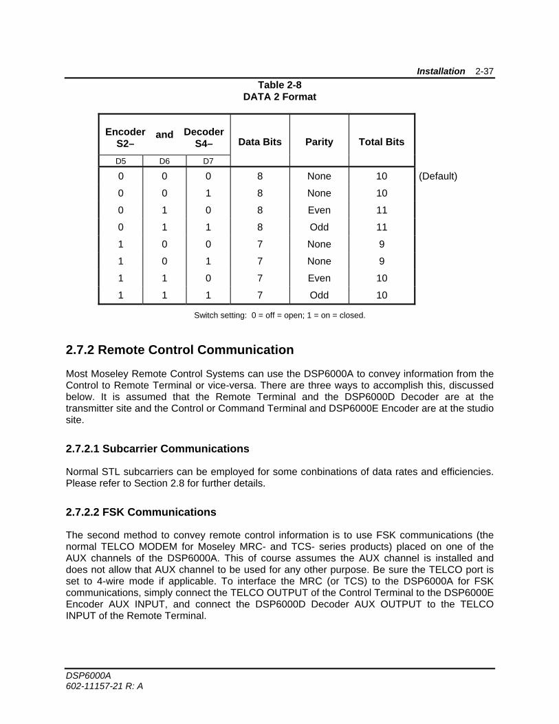
Table 2-8 DATA 2 Format
Encoder S2–
and Decoder S4– Data Bits Parity Total Bits
D5 D6 D7
0 0 0 8 None 10 (Default)
0 0 1 8 None 10
0 1 0 8 Even 11
0 1 1 8 Odd 11
1 0 0 7 None 9
1 0 1 7 None 9
1 1 0 7 Even 10
1 1 1 7 Odd 10
Switch setting: 0 = off = open; 1 = on = closed.
2.7.2 Remote Control Communication
Most Moseley Remote Control Systems can use the DSP6000A to convey information from the Control to Remote Terminal or vice-versa. There are three ways to accomplish this, discussed below. It is assumed that the Remote Terminal and the DSP6000D Decoder are at the transmitter site and the Control or Command Terminal and DSP6000E Encoder are at the studio site.
2.7.2.1 Subcarrier Communications
Normal STL subcarriers can be employed for some conbinations of data rates and efficiencies. Please refer to Section 2.8 for further details.
2.7.2.2 FSK Communications
The second method to convey remote control information is to use FSK communications (the normal TELCO MODEM for Moseley MRC- and TCS- series products) placed on one of the AUX channels of the DSP6000A. This of course assumes the AUX channel is installed and does not allow that AUX channel to be used for any other purpose. Be sure the TELCO port is set to 4-wire mode if applicable. To interface the MRC (or TCS) to the DSP6000A for FSK communications, simply connect the TELCO OUTPUT of the Control Terminal to the DSP6000E Encoder AUX INPUT, and connect the DSP6000D Decoder AUX OUTPUT to the TELCO INPUT of the Remote Terminal.
Installation 2-38
DSP6000A 602-11157-21 R: A
2.7.2.3 RS-232 Communications
The third method to convey remote control information is to use the built-in data port(s) of the DSP6000A. Because of technology changes over the years, each system is different and must be configured differently. Be sure to match the cabling, data rates, and formats with the particular system being used, referring to Table 2-9 for assistance.
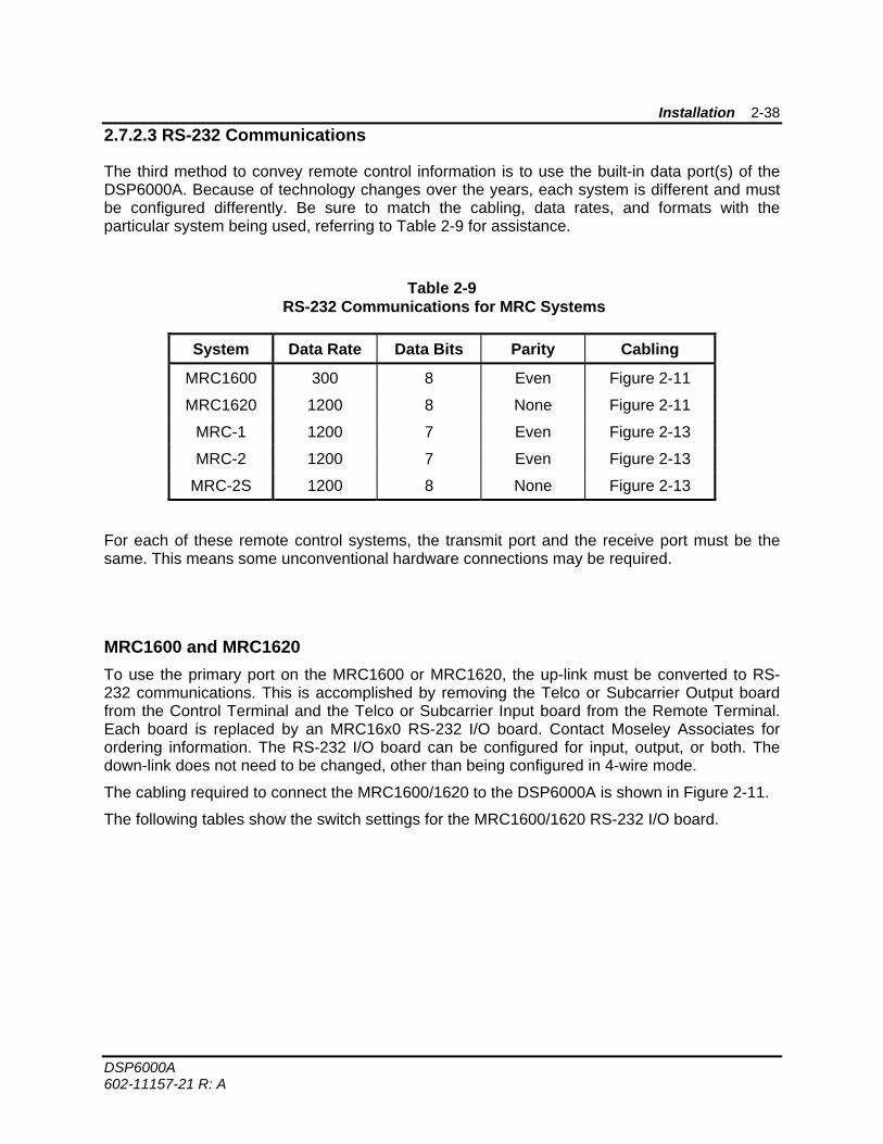
Table 2-9 RS-232 Communications for MRC Systems
System Data Rate Data Bits Parity Cabling
MRC1600 300 8 Even Figure 2-11
MRC1620 1200 8 None Figure 2-11
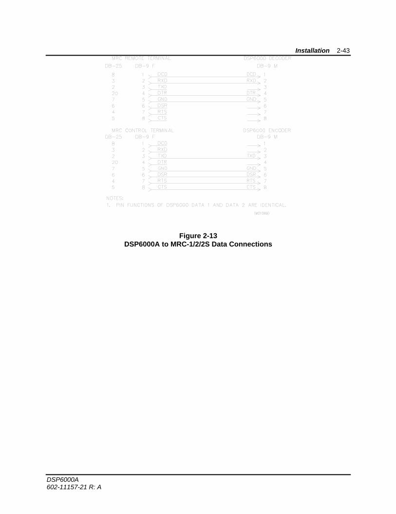
MRC-1 1200 7 Even Figure 2-13
MRC-2 1200 7 Even Figure 2-13
MRC-2S 1200 8 None Figure 2-13
For each of these remote control systems, the transmit port and the receive port must be the same. This means some unconventional hardware connections may be required.
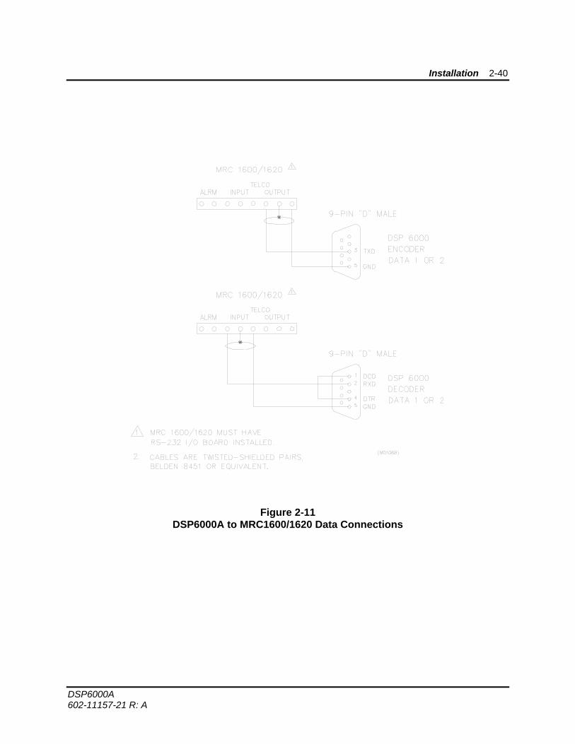
MRC1600 and MRC1620 To use the primary port on the MRC1600 or MRC1620, the up-link must be converted to RS-232 communications. This is accomplished by removing the Telco or Subcarrier Output board from the Control Terminal and the Telco or Subcarrier Input board from the Remote Terminal. Each board is replaced by an MRC16x0 RS-232 I/O board. Contact Moseley Associates for ordering information. The RS-232 I/O board can be configured for input, output, or both. The down-link does not need to be changed, other than being configured in 4-wire mode.
The cabling required to connect the MRC1600/1620 to the DSP6000A is shown in Figure 2-11.
The following tables show the switch settings for the MRC1600/1620 RS-232 I/O board.
Installation 2-39
DSP6000A 602-11157-21 R: A
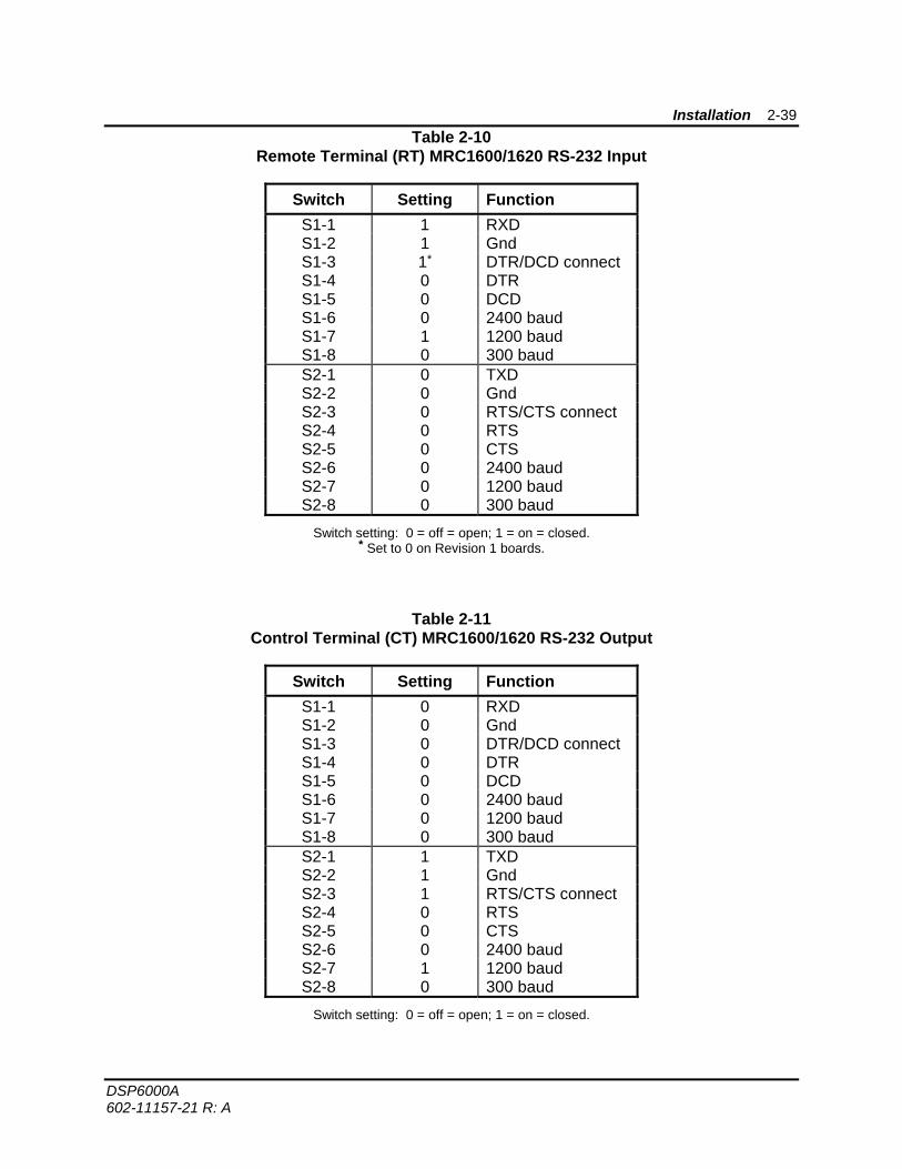
Table 2-10 Remote Terminal (RT) MRC1600/1620 RS-232 Input
Switch Setting Function S1-1 1 RXD S1-2 1 Gnd S1-3 1* DTR/DCD connect S1-4 0 DTR S1-5 0 DCD S1-6 0 2400 baud S1-7 1 1200 baud S1-8 0 300 baud S2-1 0 TXD S2-2 0 Gnd S2-3 0 RTS/CTS connect S2-4 0 RTS S2-5 0 CTS S2-6 0 2400 baud S2-7 0 1200 baud S2-8 0 300 baud
Switch setting: 0 = off = open; 1 = on = closed. * Set to 0 on Revision 1 boards.
Table 2-11 Control Terminal (CT) MRC1600/1620 RS-232 Output
Switch Setting Function S1-1 0 RXD S1-2 0 Gnd S1-3 0 DTR/DCD connect S1-4 0 DTR S1-5 0 DCD S1-6 0 2400 baud S1-7 0 1200 baud S1-8 0 300 baud S2-1 1 TXD S2-2 1 Gnd S2-3 1 RTS/CTS connect S2-4 0 RTS S2-5 0 CTS S2-6 0 2400 baud S2-7 1 1200 baud S2-8 0 300 baud
Switch setting: 0 = off = open; 1 = on = closed.
Installation 2-40
DSP6000A 602-11157-21 R: A
Figure 2-11 DSP6000A to MRC1600/1620 Data Connections
Installation 2-41
DSP6000A 602-11157-21 R: A
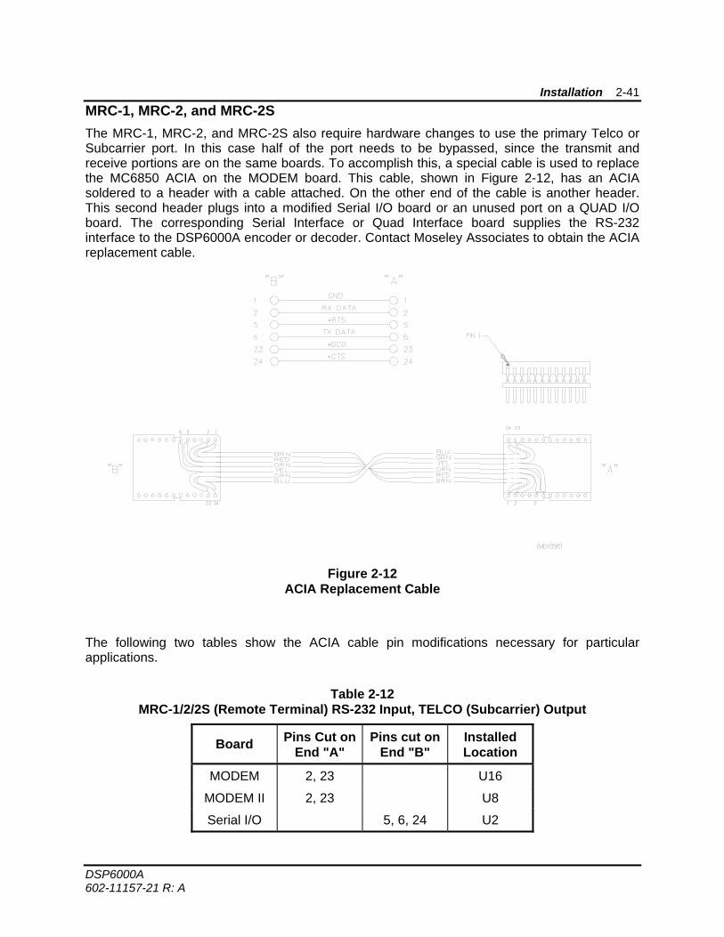
MRC-1, MRC-2, and MRC-2S The MRC-1, MRC-2, and MRC-2S also require hardware changes to use the primary Telco or Subcarrier port. In this case half of the port needs to be bypassed, since the transmit and receive portions are on the same boards. To accomplish this, a special cable is used to replace the MC6850 ACIA on the MODEM board. This cable, shown in Figure 2-12, has an ACIA soldered to a header with a cable attached. On the other end of the cable is another header. This second header plugs into a modified Serial I/O board or an unused port on a QUAD I/O board. The corresponding Serial Interface or Quad Interface board supplies the RS-232 interface to the DSP6000A encoder or decoder. Contact Moseley Associates to obtain the ACIA replacement cable.
Figure 2-12 ACIA Replacement Cable
The following two tables show the ACIA cable pin modifications necessary for particular applications.
Table 2-12 MRC-1/2/2S (Remote Terminal) RS-232 Input, TELCO (Subcarrier) Output
Board Pins Cut on End "A"
Pins cut on End "B"
Installed Location
MODEM 2, 23 U16
MODEM II 2, 23 U8
Serial I/O 5, 6, 24 U2
Installation 2-42
DSP6000A 602-11157-21 R: A
Quad I/O 5, 6, 24 U1
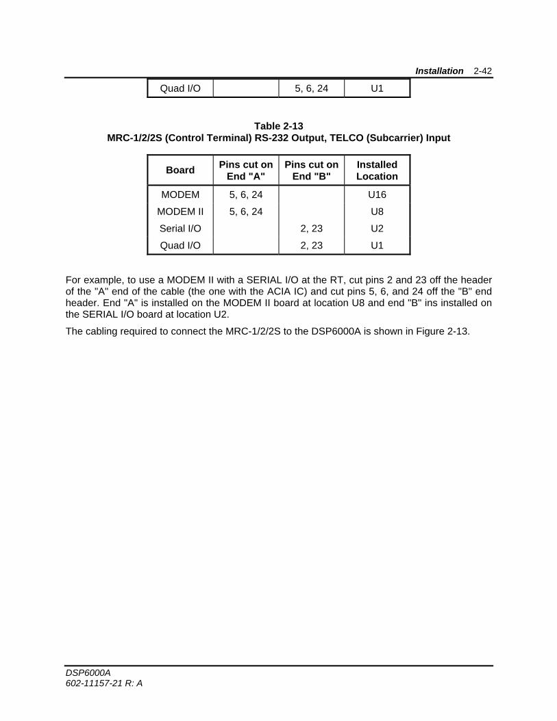
Table 2-13 MRC-1/2/2S (Control Terminal) RS-232 Output, TELCO (Subcarrier) Input
Board Pins cut on End "A"
Pins cut on End "B"
Installed Location
MODEM 5, 6, 24 U16
MODEM II 5, 6, 24 U8
Serial I/O 2, 23 U2
Quad I/O 2, 23 U1
For example, to use a MODEM II with a SERIAL I/O at the RT, cut pins 2 and 23 off the header of the "A" end of the cable (the one with the ACIA IC) and cut pins 5, 6, and 24 off the "B" end header. End "A" is installed on the MODEM II board at location U8 and end "B" ins installed on the SERIAL I/O board at location U2.
The cabling required to connect the MRC-1/2/2S to the DSP6000A is shown in Figure 2-13.
Installation 2-43
DSP6000A 602-11157-21 R: A
Figure 2-13 DSP6000A to MRC-1/2/2S Data Connections
Installation 2-44
DSP6000A 602-11157-21 R: A
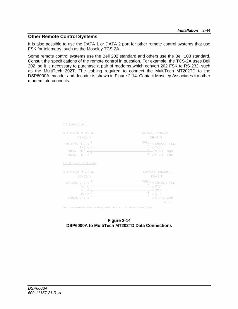
Other Remote Control Systems It is also possible to use the DATA 1 or DATA 2 port for other remote control systems that use FSK for telemetry, such as the Moseley TCS-2A.
Some remote control systems use the Bell 202 standard and others use the Bell 103 standard. Consult the specifications of the remote control in question. For example, the TCS-2A uses Bell 202, so it is necessary to purchase a pair of modems which convert 202 FSK to RS-232, such as the MultiTech 202T. The cabling required to connect the MultiTech MT202TD to the DSP6000A encoder and decoder is shown in Figure 2-14. Contact Moseley Associates for other modem interconnects.
Figure 2-14 DSP6000A to MultiTech MT202TD Data Connections
Installation 2-45
DSP6000A 602-11157-21 R: A
The MT202TD switch settings are as follows:
Table 2-14 MT202TD Settings
Switch Setting Function 1 On Suppress Local Copy 2 Off 4-wire mode 3 Off 4-wire mode 4 On 4-wire mode 5 On 0 dBm output 6 Off RTS is controlled 7 Off Squelch off
Connect the Remote Terminal Telco Output to the modem Telco Input. Connect the modem RS-232 port to the DSP6000A as outlined above for MRC-1/2/2S systems.
Connect the Control (Command) Terminal Telco Input to the other modem Telco Output. Connect the modem RS-232 port to the DSP6000A as outlined above for MRC-1/2/2S.
Be sure to set the baud rate and data format according to the remote control specifications.
Another alternative is to bypass the FSK portion of the remote control internal modem and convert the internal TTL levels to RS-232 levels using appropriate RS-232 line driver ICs (such as the MC1488) and/or receiver ICs (such as the MC1489) available from several IC manufacturers.
Installation 2-46
DSP6000A 602-11157-21 R: A
2.8 Retrofit STL Installation
If the DSP6000A codec is purchased independently from, or as an add-on to, the Studio-Transmitter Link radio, it may be necessary to perform minor alignment or modification to the STL system. This will depend on the STL model. The STL models covered in this section are:
• PCL6000
• PCL606/C (composite)
• PCL606 (mono)
• PCL505 (composite)
• Other STL radios
Refer to Section 2.5 for details on setting program levels and program and data connections.
2.8.1 PCL6010 Transmitter
Connection Refer to Section 2.5.1 for connection of encoder to PCL6010 STL transmitter.
Audio PS board Configure the jumpers on the transmitter Audio/PS board as follows:
Table 2-15 PCL6010 Audio/PS Settings
Jumper Description Position
E2 PHASE SELECT A
E3 MONO/COMP COMP
E7* MONO/COMP/DIG DIG
E8* MONO/COMP/DIG DIG
E9* MONO/COMP/DIG DIG
*On earlier PCL6010 systems with SEC jumper position, set E7 to COMP position and E8 and E9 to SEC position.
Carrier Deviation The encoder level into the transmitter determines the carrier deviation. For standard composite operation, the transmitter deviation is calibrated to ±50 kHz for COMP input level of 3.5 Vp-p. No
Installation 2-47
DSP6000A 602-11157-21 R: A
adjustment or recalibration of the transmitter deviation is required. This allows quick reconversion to the original analog transmitter configuration for emergencies, etc.
Meter Calibration Meter adjustment is required only on earlier PCL6010 systems with an SEC jumper position. With the encoder operating into the transmitter, adjust R203 PGM MTRG on the transmitter audio board until the meter reading is again 0 dB. On earlier PCL6010 systems that do not have MONO/COMP/SEC-DIG program level selection (E8/E9), adjust R160 PGM for a meter reading of 0 dB.
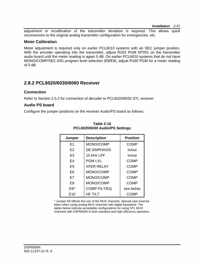
2.8.2 PCL6020/6030/6060 Receiver
Connection Refer to Section 2.5.2 for connection of decoder to PCL6020/6030 STL receiver.
Audio PS board Configure the jumper positions on the receiver Audio/PS board as follows:
Table 2-16 PCL6020/6030 Audio/PS Settings
Jumper Description Position E1 MONO/COMP COMP E2 DE-EMPHASIS in/out E3 15 kHz LPF in/out E4 PGM LVL COMP E5 XFER RELAY COMP E6 MONO/COMP COMP E7 MONO/COMP COMP E8 MONO/COMP COMP E9* COMP FILT/EQ see below E10 HF TILT COMP
* Jumper E9 effects the use of the MUX channels. Special care must be taken when using analog MUX channels with digital baseband. The tables below indicate acceptable configurations for using STL MUX channels with DSP6000A in both standard and high efficiency operation.
Installation 2-48
DSP6000A 602-11157-21 R: A
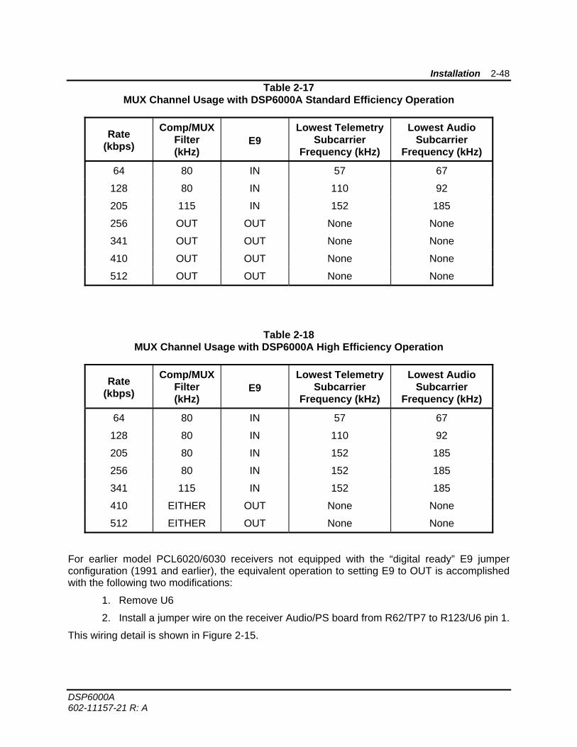
Table 2-17 MUX Channel Usage with DSP6000A Standard Efficiency Operation
Rate (kbps)
Comp/MUX Filter (kHz)
E9 Lowest Telemetry
Subcarrier Frequency (kHz)
Lowest Audio Subcarrier
Frequency (kHz)
64 80 IN 57 67
128 80 IN 110 92
205 115 IN 152 185
256 OUT OUT None None
341 OUT OUT None None
410 OUT OUT None None
512 OUT OUT None None
Table 2-18 MUX Channel Usage with DSP6000A High Efficiency Operation
Rate (kbps)
Comp/MUX Filter (kHz)
E9 Lowest Telemetry
Subcarrier Frequency (kHz)
Lowest Audio Subcarrier
Frequency (kHz)
64 80 IN 57 67
128 80 IN 110 92
205 80 IN 152 185
256 80 IN 152 185
341 115 IN 152 185
410 EITHER OUT None None
512 EITHER OUT None None
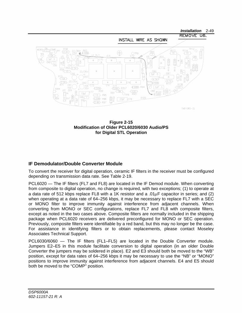
For earlier model PCL6020/6030 receivers not equipped with the “digital ready” E9 jumper configuration (1991 and earlier), the equivalent operation to setting E9 to OUT is accomplished with the following two modifications:
1. Remove U6
2. Install a jumper wire on the receiver Audio/PS board from R62/TP7 to R123/U6 pin 1.
This wiring detail is shown in Figure 2-15.
Installation 2-49
DSP6000A 602-11157-21 R: A
Figure 2-15 Modification of Older PCL6020/6030 Audio/PS
for Digital STL Operation
IF Demodulator/Double Converter Module To convert the receiver for digital operation, ceramic IF filters in the receiver must be configured depending on transmission data rate. See Table 2-19.
PCL6020 — The IF filters (FL7 and FL8) are located in the IF Demod module. When converting from composite to digital operation, no change is required, with two exceptions; (1) to operate at a data rate of 512 kbps replace FL8 with a 1K resistor and a .01μF capacitor in series; and (2) when operating at a data rate of 64–256 kbps, it may be necessary to replace FL7 with a SEC or MONO filter to improve immunity against interference from adjacent channels. When converting from MONO or SEC configurations, replace FL7 and FL8 with composite filters, except as noted in the two cases above. Composite filters are normally included in the shipping package when PCL6020 receivers are delivered preconfigured for MONO or SEC operation. Previously, composite filters were identifiable by a red band, but this may no longer be the case. For assistance in identifying filters or to obtain replacements, please contact Moseley Associates Technical Support.
PCL6030/6060 — The IF filters (FL1–FL5) are located in the Double Converter module. Jumpers E2–E5 in this module facilitate conversion to digital operation (in an older Double Converter the jumpers may be soldered in place). E2 and E3 should both be moved to the “WB” position, except for data rates of 64–256 kbps it may be necessary to use the “NB” or “MONO” positions to improve immunity against interference from adjacent channels. E4 and E5 should both be moved to the “COMP” position.
Installation 2-50
DSP6000A 602-11157-21 R: A
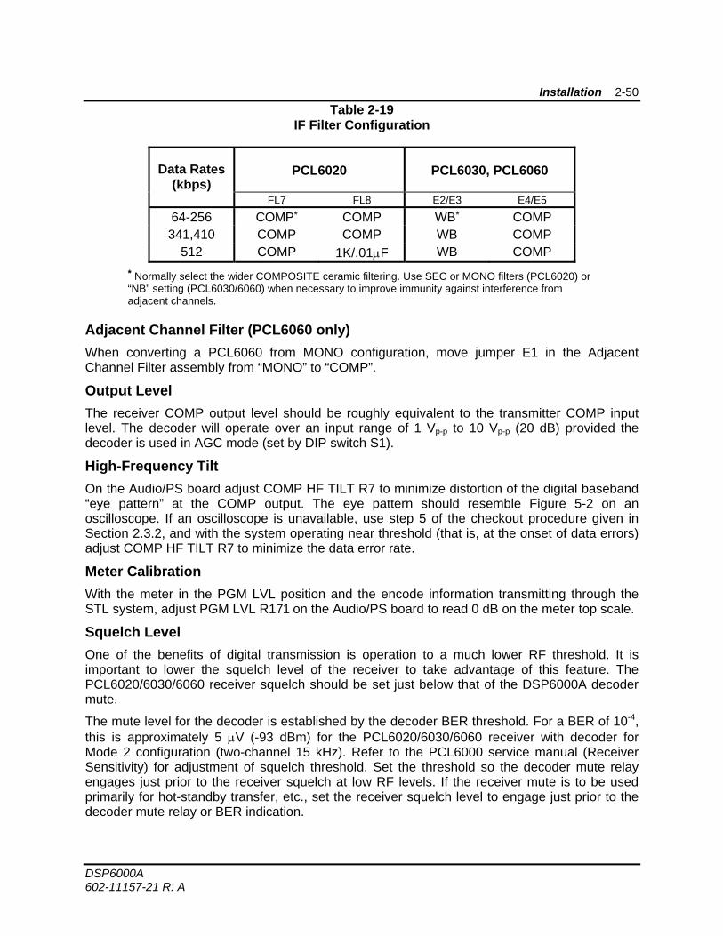
Table 2-19 IF Filter Configuration
Data Rates (kbps)
PCL6020 PCL6030, PCL6060
FL7 FL8 E2/E3 E4/E5
64-256 COMP* COMP WB* COMP 341,410 COMP COMP WB COMP
512 COMP 1K/.01μF WB COMP * Normally select the wider COMPOSITE ceramic filtering. Use SEC or MONO filters (PCL6020) or “NB” setting (PCL6030/6060) when necessary to improve immunity against interference from adjacent channels.
Adjacent Channel Filter (PCL6060 only) When converting a PCL6060 from MONO configuration, move jumper E1 in the Adjacent Channel Filter assembly from “MONO” to “COMP”.
Output Level The receiver COMP output level should be roughly equivalent to the transmitter COMP input level. The decoder will operate over an input range of 1 Vp-p to 10 Vp-p (20 dB) provided the decoder is used in AGC mode (set by DIP switch S1).
High-Frequency Tilt On the Audio/PS board adjust COMP HF TILT R7 to minimize distortion of the digital baseband “eye pattern” at the COMP output. The eye pattern should resemble Figure 5-2 on an oscilloscope. If an oscilloscope is unavailable, use step 5 of the checkout procedure given in Section 2.3.2, and with the system operating near threshold (that is, at the onset of data errors) adjust COMP HF TILT R7 to minimize the data error rate.
Meter Calibration With the meter in the PGM LVL position and the encode information transmitting through the STL system, adjust PGM LVL R171 on the Audio/PS board to read 0 dB on the meter top scale.
Squelch Level One of the benefits of digital transmission is operation to a much lower RF threshold. It is important to lower the squelch level of the receiver to take advantage of this feature. The PCL6020/6030/6060 receiver squelch should be set just below that of the DSP6000A decoder mute.
The mute level for the decoder is established by the decoder BER threshold. For a BER of 10-4, this is approximately 5 μV (-93 dBm) for the PCL6020/6030/6060 receiver with decoder for Mode 2 configuration (two-channel 15 kHz). Refer to the PCL6000 service manual (Receiver Sensitivity) for adjustment of squelch threshold. Set the threshold so the decoder mute relay engages just prior to the receiver squelch at low RF levels. If the receiver mute is to be used primarily for hot-standby transfer, etc., set the receiver squelch level to engage just prior to the decoder mute relay or BER indication.
Installation 2-51
DSP6000A 602-11157-21 R: A
2.8.3 PCL606 Transmitter, Mono
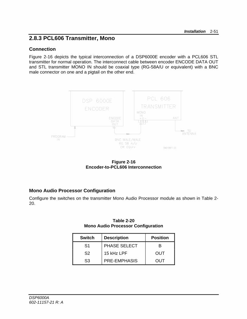
Connection Figure 2-16 depicts the typical interconnection of a DSP6000E encoder with a PCL606 STL transmitter for normal operation. The interconnect cable between encoder ENCODE DATA OUT and STL transmitter MONO IN should be coaxial type (RG-58A/U or equivalent) with a BNC male connector on one and a pigtail on the other end.
Figure 2-16 Encoder-to-PCL606 Interconnection
Mono Audio Processor Configuration Configure the switches on the transmitter Mono Audio Processor module as shown in Table 2-20.
Table 2-20 Mono Audio Processor Configuration
Switch Description Position
S1 PHASE SELECT B
S2 15 kHz LPF OUT
S3 PRE-EMPHASIS OUT
Installation 2-52
DSP6000A 602-11157-21 R: A
NOTE
In an old system, reduced reliability may be experienced in mechanical switches. Moseley recommends hardwiring switches S1, S1, and S3 into the appropriate configuration with wire jumpers.
We also recommend removal of resistor R93 (600 ohm) to reduce loading of the output of the encoder. Otherwise, it is necessary to compensate for this load by increasing the output level of the encoder.
Carrier Deviation For standard mono operation, the transmitter carrier deviation is calibrated to ±40 kHz for MONO IN input level of +10 dBm (6.93 Vp-p). Recalibrate the transmitter carrier deviation to ±50 kHz for input level of 3.5 Vp-p. Refer to Section 6.3.4 of the PCL606 service manual for deviation adjustment.
An alternative is available to avoid recalibration of carrier deviation and speed installation. Instead, recalibrate the encoder OUTPUT DATA level. It will be necessary to recalculate encoder output level as described in step #4 (Encoder Output Level) of the alignment procedure given in Section 5.3 (Encoder Alignment). In this case, however, do not adjust transmitter deviation. This has the advantage of allowing quick reconversion to the original analog configuration. For example, when operating at a transmission rate of 256 kbps, set ENCODE OUTPUT LEVEL = 11.03 Vp-p to produce 64 kHz deviation (0.0431 × 256 = 11.03). If the encoder output level has been recalibrated, the levels given in Table 5-6 for various configurations will be inaccurate.
Meter Calibration With the encoder operating into the transmitter, adjust PGM R3 on the transmitter Metering and Status board until the meter reading is again 0 dB.
Installation 2-53
DSP6000A 602-11157-21 R: A
2.8.4 PCL606 Receiver, Mono
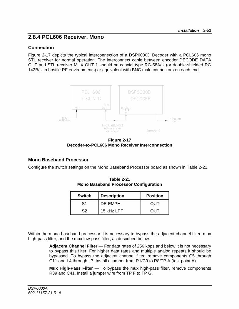
Connection Figure 2-17 depicts the typical interconnection of a DSP6000D Decoder with a PCL606 mono STL receiver for normal operation. The interconnect cable between encoder DECODE DATA OUT and STL receiver MUX OUT 1 should be coaxial type RG-58A/U (or double-shielded RG 142B/U in hostile RF environments) or equivalent with BNC male connectors on each end.
Figure 2-17 Decoder-to-PCL606 Mono Receiver Interconnection
Mono Baseband Processor Configure the switch settings on the Mono Baseband Processor board as shown in Table 2-21.
Table 2-21 Mono Baseband Processor Configuration
Switch Description Position
S1 DE-EMPH OUT
S2 15 kHz LPF OUT
Within the mono baseband processor it is necessary to bypass the adjacent channel filter, mux high-pass filter, and the mux low-pass filter, as described below.
Adjacent Channel Filter — For data rates of 256 kbps and below it is not necessary to bypass this filter. For higher data rates and multiple analog repeats it should be bypassed. To bypass the adjacent channel filter, remove components C5 through C11 and L4 through L7. Install a jumper from R1/C9 to R8/TP A (test point A).
Mux High-Pass Filter — To bypass the mux high-pass filter, remove components R39 and C41. Install a jumper wire from TP F to TP G.
Installation 2-54
DSP6000A 602-11157-21 R: A
Mux Low-Pass Filter — To bypass the mux low-pass filter, remove components C57, C58, C59, and L10. Remove R92 on the mux buffer. Install a jumper wire from TP H to TP I.
Double Converter The PCL606 mono STL receiver is supplied with ceramic IF filters of 250 kHz bandwidth. These filters are FL1 and FL2, located in the double converter. These filters are generally too narrow to pass the "digital" baseband information, but are adequate for transmission data rates of 256 kbps and below. For transmission data rates above 256 kbps to below 512 kbps, replace FL1 and FL2 with composite ceramic IF filters (available from Moseley Associates). For operation at 512 kbps, replace FL1 with a composite ceramic filter and replace FL2 with a 1 kohm resistor.
High-Frequency Gain Correction Within the Mono Baseband Processor module adjust HF TILT R11 to minimize distortion of the digital baseband “eye pattern” at the MUX output. The eye pattern should resemble Figure 5-2 on an oscilloscope. Alternatively, if an oscilloscope is unavailable, use step #5 of the checkout procedure given in Section 2.3.2, and with the system operating near RF threshold (that is, at the onset of data errors), adjust HF TILT R11 to minimize the data error rate.
Output Level The receiver output is found at the MUX OUT 1 BNC connector. The analog mux facility is not available in the digital STL configuration. Adjust MUX LEVEL R64 to set MUX OUT 1 level approximately equivalent to the transmitter COMP input level. The decoder will operate over an input range of 1 Vp-p to 10 Vp-p (20 dB) or more as long as the decoder is used in AGC mode (set by DIP switch S1).
Meter Calibration With the meter in the MUX LVL position and the encoder data transmitting through the STL system, adjust MUX LVL R2 to read 0 dB on the meter top scale.
Squelch Level One of the benefits of digital transmission is operation to a much lower RF threshold. It is important to lower the squelch level of the receiver to take advantage of this feature. The receiver squelch should be set just below that of the decoder mute.
The mute level for the decoder is established by the decoder BER threshold. For a BER of 10-4, this is approximately 5 μV (-93 dBm) for the PCL6020 receiver with decoder in Mode 2 configuration (two-channel 15 kHz). Refer to the PCL606 service manual (Section 6.3.2 Receiver Sensitivity) for adjustment of squelch threshold. Set the threshold so the decoder mute relay engages just prior to the receiver squelch at low RF levels. If the receiver mute is to be used primarily for hot-standby transfer, etc., set the receiver squelch level to engage just prior to the decoder mute relay or BER indication.
Installation 2-55
DSP6000A 602-11157-21 R: A
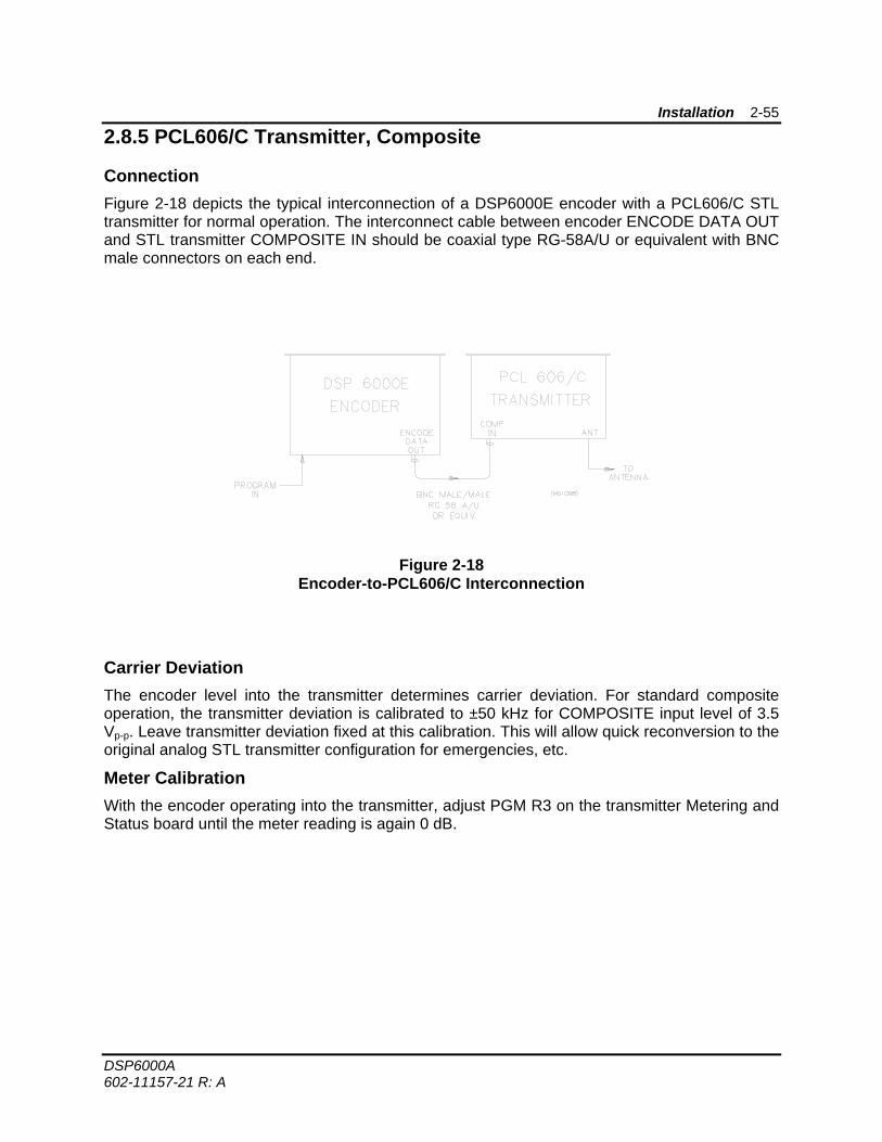
2.8.5 PCL606/C Transmitter, Composite
Connection Figure 2-18 depicts the typical interconnection of a DSP6000E encoder with a PCL606/C STL transmitter for normal operation. The interconnect cable between encoder ENCODE DATA OUT and STL transmitter COMPOSITE IN should be coaxial type RG-58A/U or equivalent with BNC male connectors on each end.
Figure 2-18 Encoder-to-PCL606/C Interconnection
Carrier Deviation The encoder level into the transmitter determines carrier deviation. For standard composite operation, the transmitter deviation is calibrated to ±50 kHz for COMPOSITE input level of 3.5 Vp-p. Leave transmitter deviation fixed at this calibration. This will allow quick reconversion to the original analog STL transmitter configuration for emergencies, etc.
Meter Calibration With the encoder operating into the transmitter, adjust PGM R3 on the transmitter Metering and Status board until the meter reading is again 0 dB.
Installation 2-56
DSP6000A 602-11157-21 R: A
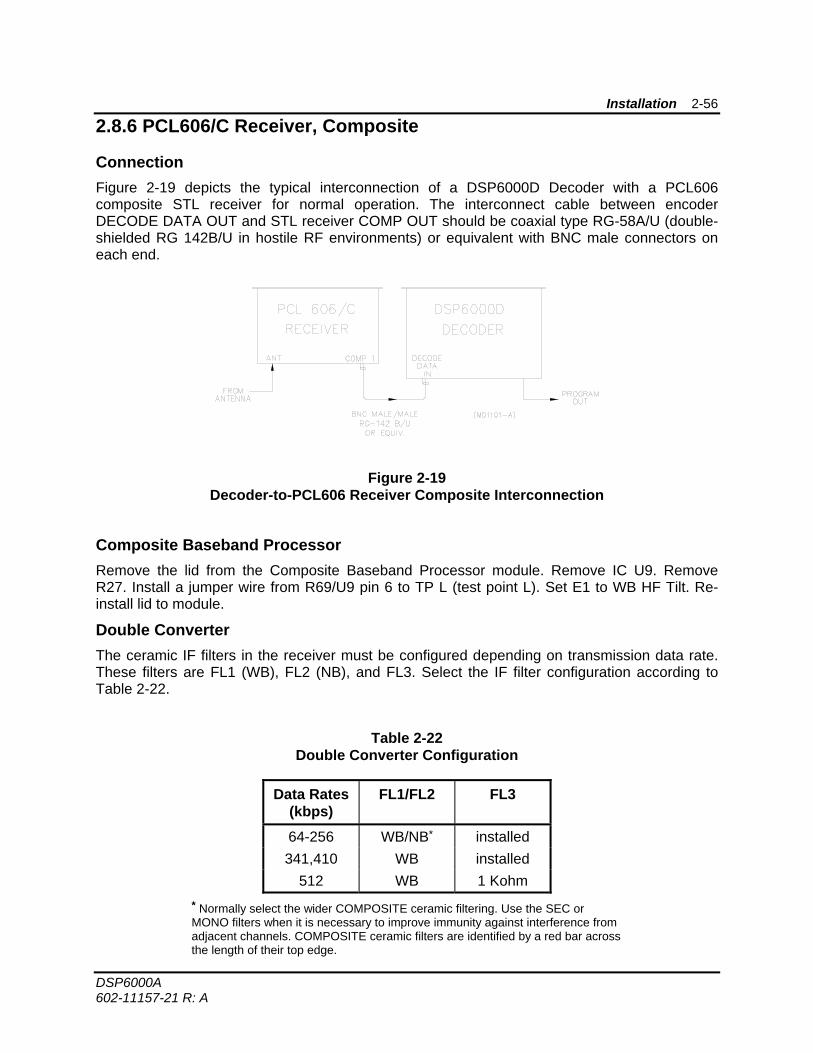
2.8.6 PCL606/C Receiver, Composite
Connection Figure 2-19 depicts the typical interconnection of a DSP6000D Decoder with a PCL606 composite STL receiver for normal operation. The interconnect cable between encoder DECODE DATA OUT and STL receiver COMP OUT should be coaxial type RG-58A/U (double-shielded RG 142B/U in hostile RF environments) or equivalent with BNC male connectors on each end.
Figure 2-19 Decoder-to-PCL606 Receiver Composite Interconnection
Composite Baseband Processor Remove the lid from the Composite Baseband Processor module. Remove IC U9. Remove R27. Install a jumper wire from R69/U9 pin 6 to TP L (test point L). Set E1 to WB HF Tilt. Re-install lid to module.
Double Converter The ceramic IF filters in the receiver must be configured depending on transmission data rate. These filters are FL1 (WB), FL2 (NB), and FL3. Select the IF filter configuration according to Table 2-22.
Table 2-22 Double Converter Configuration
Data Rates (kbps)
FL1/FL2 FL3
64-256 WB/NB* installed 341,410 WB installed
512 WB 1 Kohm * Normally select the wider COMPOSITE ceramic filtering. Use the SEC or MONO filters when it is necessary to improve immunity against interference from adjacent channels. COMPOSITE ceramic filters are identified by a red bar across the length of their top edge.
Installation 2-57
DSP6000A 602-11157-21 R: A
High-Frequency Gain Correction Within the Composite Baseband Processor module adjust HF TILT WB R10 to minimize distortion of the digital baseband “eye-pattern” at the COMP 1 output. The eye pattern should resemble Figure 5-2 on an oscilloscope. Alternatively, if an oscilloscope is unavailable, use step #5 of the checkout procedure given in Section 2.3.2, and with the system operating near threshold (that is, at the onset of data errors) adjust HF TILT R11 to minimize the data error rate.
Output Level The receiver output is found at the COMP 1 BNC connector. The receiver COMP 1 level should be roughly equivalent to the transmitter COMP input level. The decoder will operate properly over an input range of 1 Vp-p to 10 Vp-p (20 dB) as long as the decoder is used in ALC mode (S1).
Meter Calibration With the meter in the PGM LVL position and the encoder data transmitting through the STL system, adjust PGM LVL R1 to read 0 dB on the meter top scale.
Squelch Level One of the benefits of digital transmission is operation to a much lower RF threshold. It is important to lower the squelch level of the receiver to take advantage of this feature. The receiver squelch should be set just below that of the decoder mute.
The mute level for the decoder is established by the decoder BER threshold. For a BER of 10-4, this is approximately 5 μV (-93 dBm) for the PCL6020 receiver with decoder in Mode 2 configuration (two-channel 15 kHz). Refer to the PCL606 service manual (Section 6.3.2 Receiver Sensitivity) for adjustment of squelch threshold. Set the threshold so the decoder mute relay engages just prior to the receiver squelch at low RF levels. If the receiver mute is to be used primarily for hot-standby transfer, etc., set the receiver squelch level to engage just prior to the decoder mute relay or BER indication.
Installation 2-58
DSP6000A 602-11157-21 R: A
2.8.7 PCL505 Transmitter, Composite
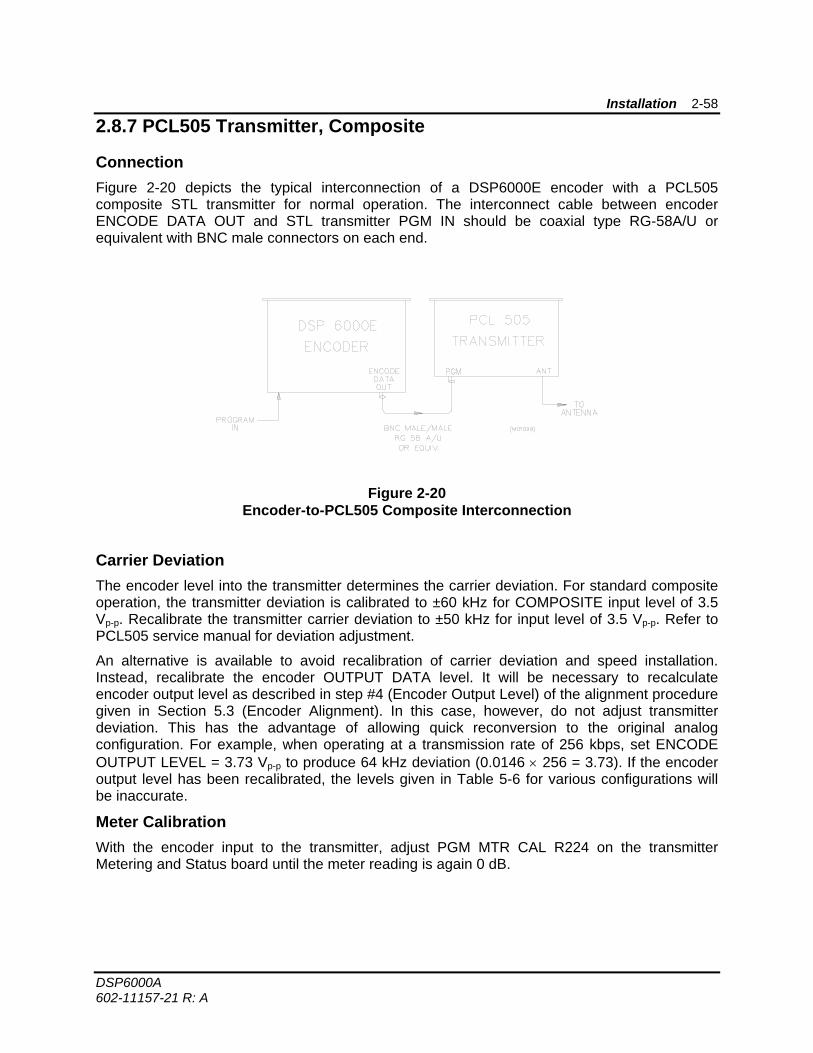
Connection Figure 2-20 depicts the typical interconnection of a DSP6000E encoder with a PCL505 composite STL transmitter for normal operation. The interconnect cable between encoder ENCODE DATA OUT and STL transmitter PGM IN should be coaxial type RG-58A/U or equivalent with BNC male connectors on each end.
Figure 2-20 Encoder-to-PCL505 Composite Interconnection
Carrier Deviation The encoder level into the transmitter determines the carrier deviation. For standard composite operation, the transmitter deviation is calibrated to ±60 kHz for COMPOSITE input level of 3.5 Vp-p. Recalibrate the transmitter carrier deviation to ±50 kHz for input level of 3.5 Vp-p. Refer to PCL505 service manual for deviation adjustment.
An alternative is available to avoid recalibration of carrier deviation and speed installation. Instead, recalibrate the encoder OUTPUT DATA level. It will be necessary to recalculate encoder output level as described in step #4 (Encoder Output Level) of the alignment procedure given in Section 5.3 (Encoder Alignment). In this case, however, do not adjust transmitter deviation. This has the advantage of allowing quick reconversion to the original analog configuration. For example, when operating at a transmission rate of 256 kbps, set ENCODE OUTPUT LEVEL = 3.73 Vp-p to produce 64 kHz deviation (0.0146 × 256 = 3.73). If the encoder output level has been recalibrated, the levels given in Table 5-6 for various configurations will be inaccurate.
Meter Calibration With the encoder input to the transmitter, adjust PGM MTR CAL R224 on the transmitter Metering and Status board until the meter reading is again 0 dB.
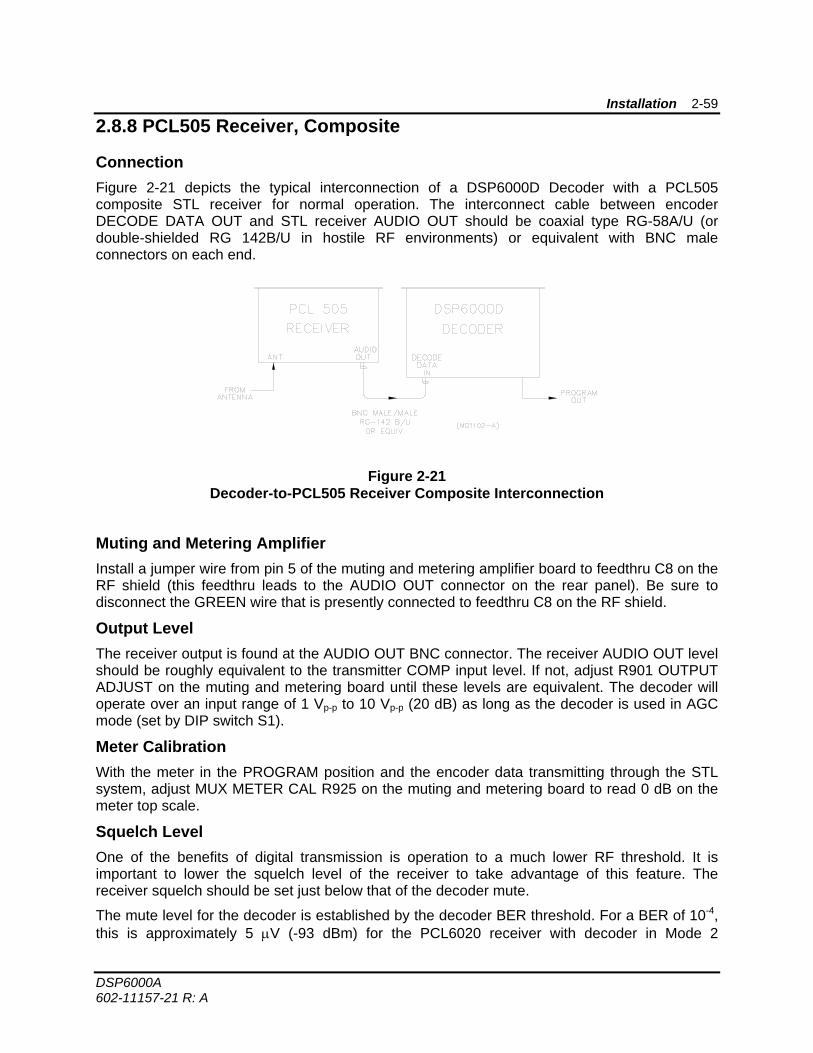
Installation 2-59
DSP6000A 602-11157-21 R: A
2.8.8 PCL505 Receiver, Composite
Connection Figure 2-21 depicts the typical interconnection of a DSP6000D Decoder with a PCL505 composite STL receiver for normal operation. The interconnect cable between encoder DECODE DATA OUT and STL receiver AUDIO OUT should be coaxial type RG-58A/U (or double-shielded RG 142B/U in hostile RF environments) or equivalent with BNC male connectors on each end.
Figure 2-21 Decoder-to-PCL505 Receiver Composite Interconnection
Muting and Metering Amplifier Install a jumper wire from pin 5 of the muting and metering amplifier board to feedthru C8 on the RF shield (this feedthru leads to the AUDIO OUT connector on the rear panel). Be sure to disconnect the GREEN wire that is presently connected to feedthru C8 on the RF shield.
Output Level The receiver output is found at the AUDIO OUT BNC connector. The receiver AUDIO OUT level should be roughly equivalent to the transmitter COMP input level. If not, adjust R901 OUTPUT ADJUST on the muting and metering board until these levels are equivalent. The decoder will operate over an input range of 1 Vp-p to 10 Vp-p (20 dB) as long as the decoder is used in AGC mode (set by DIP switch S1).
Meter Calibration With the meter in the PROGRAM position and the encoder data transmitting through the STL system, adjust MUX METER CAL R925 on the muting and metering board to read 0 dB on the meter top scale.
Squelch Level One of the benefits of digital transmission is operation to a much lower RF threshold. It is important to lower the squelch level of the receiver to take advantage of this feature. The receiver squelch should be set just below that of the decoder mute.
The mute level for the decoder is established by the decoder BER threshold. For a BER of 10-4, this is approximately 5 μV (-93 dBm) for the PCL6020 receiver with decoder in Mode 2
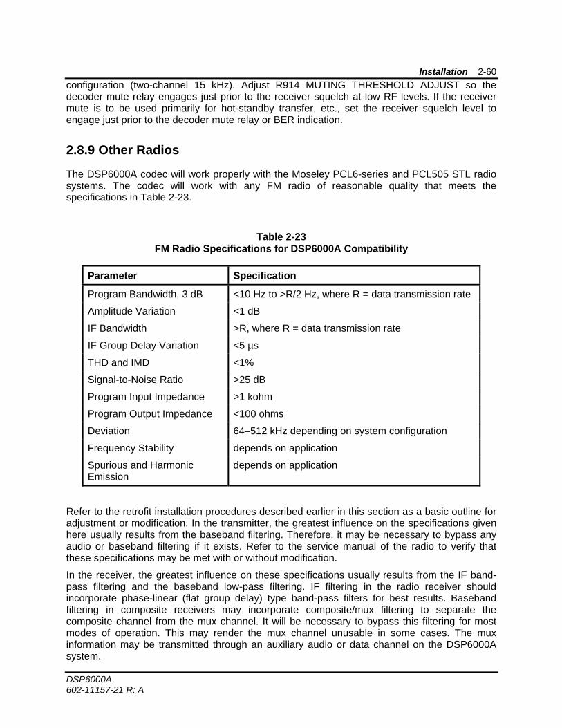
Installation 2-60
DSP6000A 602-11157-21 R: A
configuration (two-channel 15 kHz). Adjust R914 MUTING THRESHOLD ADJUST so the decoder mute relay engages just prior to the receiver squelch at low RF levels. If the receiver mute is to be used primarily for hot-standby transfer, etc., set the receiver squelch level to engage just prior to the decoder mute relay or BER indication.
2.8.9 Other Radios
The DSP6000A codec will work properly with the Moseley PCL6-series and PCL505 STL radio systems. The codec will work with any FM radio of reasonable quality that meets the specifications in Table 2-23.
Table 2-23 FM Radio Specifications for DSP6000A Compatibility
Parameter Specification
Program Bandwidth, 3 dB <10 Hz to >R/2 Hz, where R = data transmission rate
Amplitude Variation <1 dB
IF Bandwidth >R, where R = data transmission rate
IF Group Delay Variation <5 µs
THD and IMD <1%
Signal-to-Noise Ratio >25 dB
Program Input Impedance >1 kohm
Program Output Impedance <100 ohms
Deviation 64–512 kHz depending on system configuration
Frequency Stability depends on application
Spurious and Harmonic Emission
depends on application
Refer to the retrofit installation procedures described earlier in this section as a basic outline for adjustment or modification. In the transmitter, the greatest influence on the specifications given here usually results from the baseband filtering. Therefore, it may be necessary to bypass any audio or baseband filtering if it exists. Refer to the service manual of the radio to verify that these specifications may be met with or without modification.
In the receiver, the greatest influence on these specifications usually results from the IF band-pass filtering and the baseband low-pass filtering. IF filtering in the radio receiver should incorporate phase-linear (flat group delay) type band-pass filters for best results. Baseband filtering in composite receivers may incorporate composite/mux filtering to separate the composite channel from the mux channel. It will be necessary to bypass this filtering for most modes of operation. This may render the mux channel unusable in some cases. The mux information may be transmitted through an auxiliary audio or data channel on the DSP6000A system.
Installation 2-61
DSP6000A 602-11157-21 R: A
The system's ability to handle radio interference from co-channel and adjacent-channel sources and simply mean-time-between-failure depends solely on the quality of the radio used. For applications requiring very high reliability or on-air time, such as an aural studio-transmitter link, good design and quality are essential.
High-quality composite-type STL radios, such as the Moseley PCL6010 and PCL606, will satisfy these requirements with little or no modification. Mono-type STL radios may require that the baseband filtering be bypassed. Also, balanced 600 ohm audio inputs found on mono systems may not be capable of handling the wider bandwidth requirements of the digital signal.
2.8.10 Retrofit Repeater Installation with STL
If existing STL radios are to be used for the repeater installation, follow the alignment procedures described above in Retrofit STL Installation appropriate to the radio being used. The basic repeater configuration is presented in Section 2.5.4 (STL Installation, Repeater). Refer to that section for a more complete understanding of the repeater installation. A complete detail of the repeater installation is shown in Figure 2-7.
DSP6000A 602-11157-31 R: A
Section 3
Operation
Section Contents Page
3.1 Encoder Front Panel 3-2 3.2 Encoder Back Panel 3-3 3.3 Encoder Pin Assignments 3-4 3.4 Decoder Front Panel 3-6 3.5 Decoder Back Panel 3-7 3.6 Decoder Pin Assignments 3-8
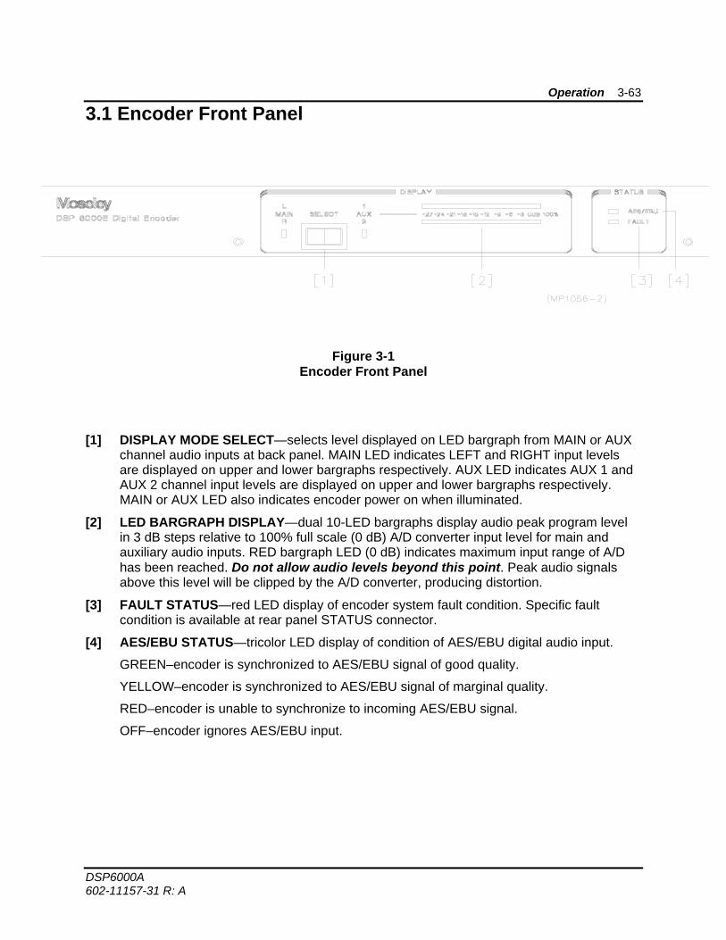
Operation 3-63
DSP6000A 602-11157-31 R: A
3.1 Encoder Front Panel
Figure 3-1 Encoder Front Panel
[1] DISPLAY MODE SELECT—selects level displayed on LED bargraph from MAIN or AUX
channel audio inputs at back panel. MAIN LED indicates LEFT and RIGHT input levels are displayed on upper and lower bargraphs respectively. AUX LED indicates AUX 1 and AUX 2 channel input levels are displayed on upper and lower bargraphs respectively. MAIN or AUX LED also indicates encoder power on when illuminated.
[2] LED BARGRAPH DISPLAY—dual 10-LED bargraphs display audio peak program level in 3 dB steps relative to 100% full scale (0 dB) A/D converter input level for main and auxiliary audio inputs. RED bargraph LED (0 dB) indicates maximum input range of A/D has been reached. Do not allow audio levels beyond this point. Peak audio signals above this level will be clipped by the A/D converter, producing distortion.
[3] FAULT STATUS—red LED display of encoder system fault condition. Specific fault condition is available at rear panel STATUS connector.
[4] AES/EBU STATUS—tricolor LED display of condition of AES/EBU digital audio input.
GREEN–encoder is synchronized to AES/EBU signal of good quality.
YELLOW–encoder is synchronized to AES/EBU signal of marginal quality.
RED–encoder is unable to synchronize to incoming AES/EBU signal.
OFF–encoder ignores AES/EBU input.
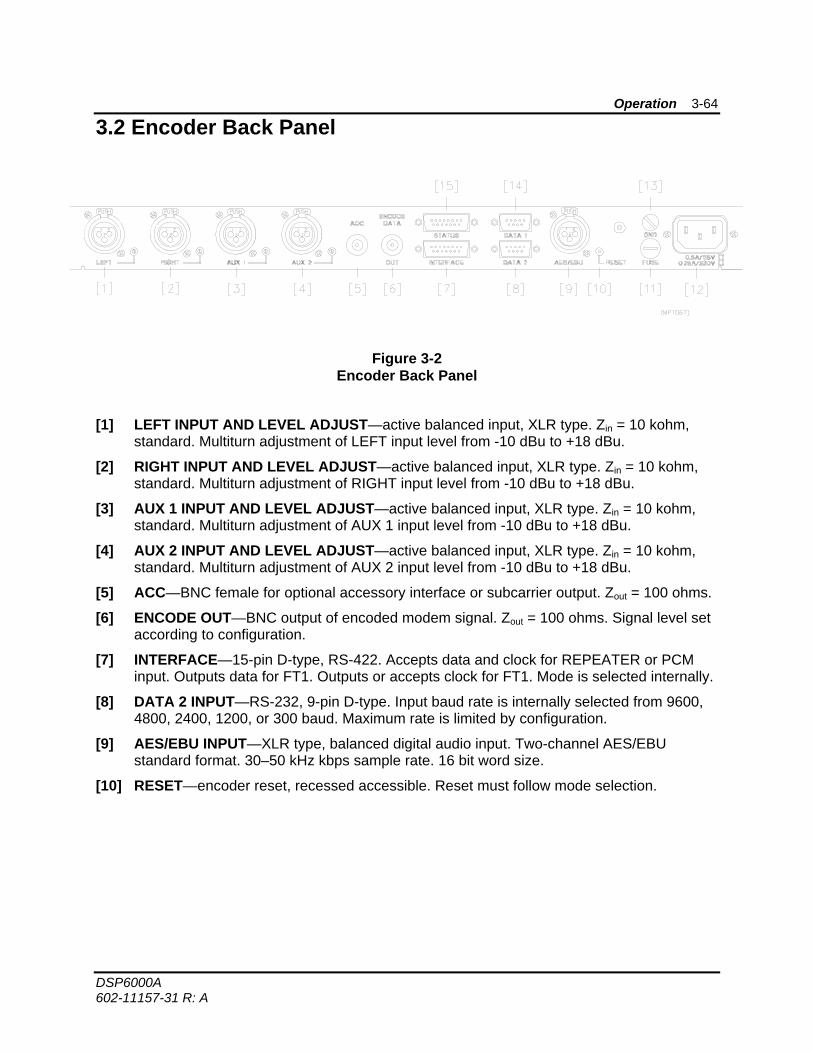
Operation 3-64
DSP6000A 602-11157-31 R: A
3.2 Encoder Back Panel
Figure 3-2 Encoder Back Panel
[1] LEFT INPUT AND LEVEL ADJUST—active balanced input, XLR type. Zin = 10 kohm, standard. Multiturn adjustment of LEFT input level from -10 dBu to +18 dBu.
[2] RIGHT INPUT AND LEVEL ADJUST—active balanced input, XLR type. Zin = 10 kohm, standard. Multiturn adjustment of RIGHT input level from -10 dBu to +18 dBu.
[3] AUX 1 INPUT AND LEVEL ADJUST—active balanced input, XLR type. Zin = 10 kohm, standard. Multiturn adjustment of AUX 1 input level from -10 dBu to +18 dBu.
[4] AUX 2 INPUT AND LEVEL ADJUST—active balanced input, XLR type. Zin = 10 kohm, standard. Multiturn adjustment of AUX 2 input level from -10 dBu to +18 dBu.
[5] ACC—BNC female for optional accessory interface or subcarrier output. Zout = 100 ohms.
[6] ENCODE OUT—BNC output of encoded modem signal. Zout = 100 ohms. Signal level set according to configuration.
[7] INTERFACE—15-pin D-type, RS-422. Accepts data and clock for REPEATER or PCM input. Outputs data for FT1. Outputs or accepts clock for FT1. Mode is selected internally.
[8] DATA 2 INPUT—RS-232, 9-pin D-type. Input baud rate is internally selected from 9600, 4800, 2400, 1200, or 300 baud. Maximum rate is limited by configuration.
[9] AES/EBU INPUT—XLR type, balanced digital audio input. Two-channel AES/EBU standard format. 30–50 kHz kbps sample rate. 16 bit word size.
[10] RESET—encoder reset, recessed accessible. Reset must follow mode selection.
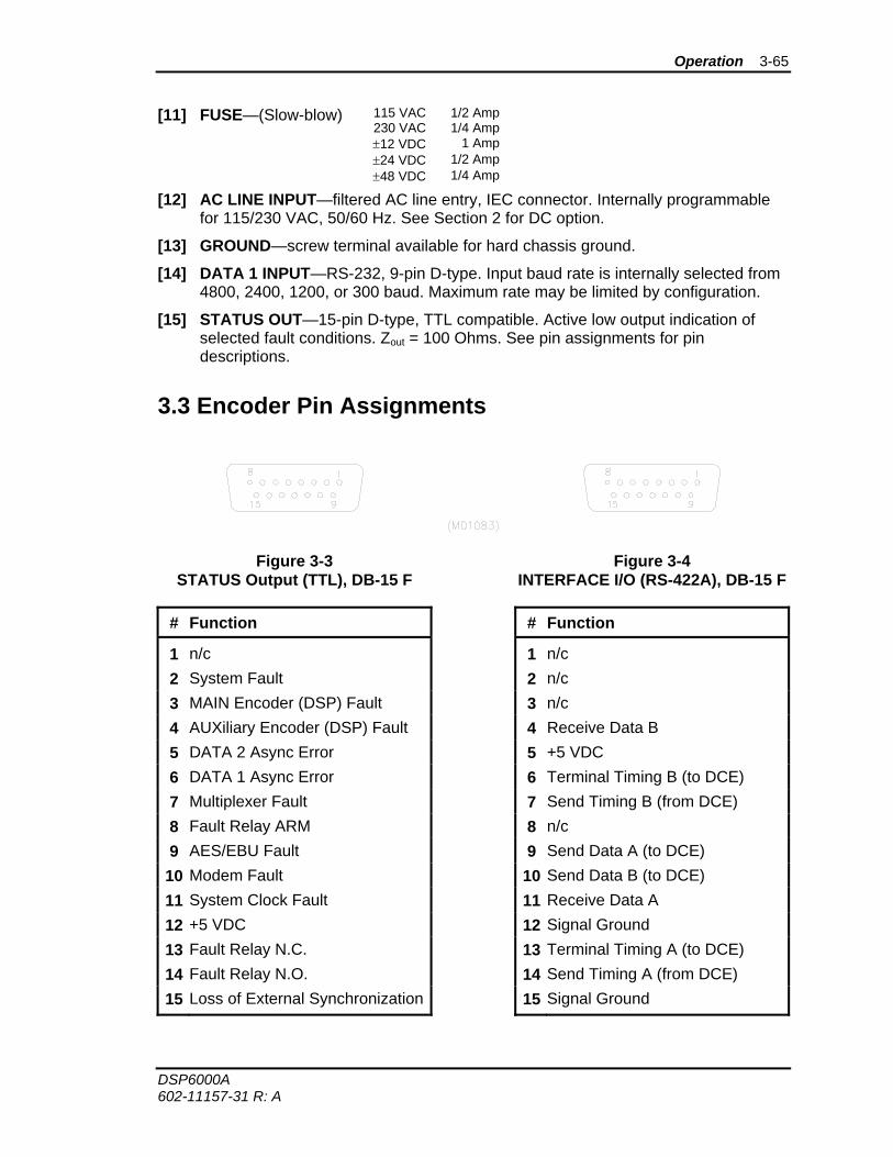
Operation 3-65
DSP6000A 602-11157-31 R: A
[11] FUSE—(Slow-blow)
115 VAC 1/2 Amp 230 VAC 1/4 Amp ±12 VDC 1 Amp ±24 VDC 1/2 Amp ±48 VDC 1/4 Amp
[12] AC LINE INPUT—filtered AC line entry, IEC connector. Internally programmable for 115/230 VAC, 50/60 Hz. See Section 2 for DC option.
[13] GROUND—screw terminal available for hard chassis ground.
[14] DATA 1 INPUT—RS-232, 9-pin D-type. Input baud rate is internally selected from 4800, 2400, 1200, or 300 baud. Maximum rate may be limited by configuration.
[15] STATUS OUT—15-pin D-type, TTL compatible. Active low output indication of selected fault conditions. Zout = 100 Ohms. See pin assignments for pin descriptions.
3.3 Encoder Pin Assignments
Figure 3-3 STATUS Output (TTL), DB-15 F
Figure 3-4 INTERFACE I/O (RS-422A), DB-15 F
# Function # Function
1 n/c 1 n/c 2 System Fault 2 n/c 3 MAIN Encoder (DSP) Fault 3 n/c 4 AUXiliary Encoder (DSP) Fault 4 Receive Data B 5 DATA 2 Async Error 5 +5 VDC 6 DATA 1 Async Error 6 Terminal Timing B (to DCE) 7 Multiplexer Fault 7 Send Timing B (from DCE) 8 Fault Relay ARM 8 n/c 9 AES/EBU Fault 9 Send Data A (to DCE)
10 Modem Fault 10 Send Data B (to DCE) 11 System Clock Fault 11 Receive Data A 12 +5 VDC 12 Signal Ground 13 Fault Relay N.C. 13 Terminal Timing A (to DCE) 14 Fault Relay N.O. 14 Send Timing A (from DCE) 15 Loss of External Synchronization 15 Signal Ground
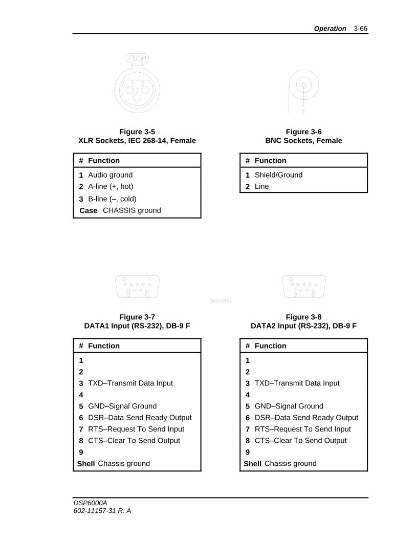
Operation 3-66
DSP6000A 602-11157-31 R: A
Figure 3-5 XLR Sockets, IEC 268-14, Female
Figure 3-6 BNC Sockets, Female
# Function # Function
1 Audio ground 1 Shield/Ground 2 A-line (+, hot) 2 Line
3 B-line (–, cold) Case CHASSIS ground
Figure 3-7 DATA1 Input (RS-232), DB-9 F
Figure 3-8 DATA2 Input (RS-232), DB-9 F
# Function # Function
1 1 2 2 3 TXD–Transmit Data Input 3 TXD–Transmit Data Input 4 4 5 GND–Signal Ground 5 GND–Signal Ground 6 DSR–Data Send Ready Output 6 DSR–Data Send Ready Output 7 RTS–Request To Send Input 7 RTS–Request To Send Input 8 CTS–Clear To Send Output 8 CTS–Clear To Send Output 9 9 Shell Chassis ground Shell Chassis ground
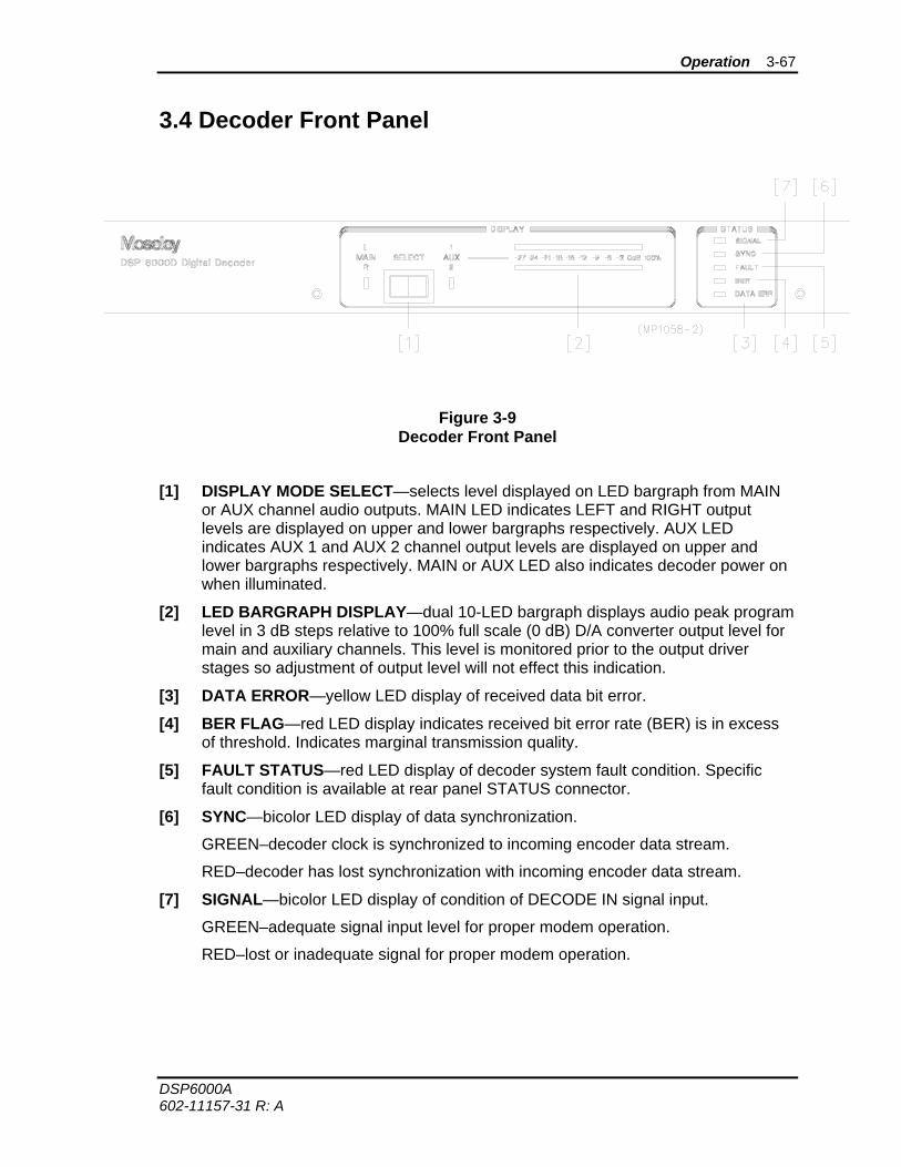
Operation 3-67
DSP6000A 602-11157-31 R: A
3.4 Decoder Front Panel
Figure 3-9 Decoder Front Panel
[1] DISPLAY MODE SELECT—selects level displayed on LED bargraph from MAIN or AUX channel audio outputs. MAIN LED indicates LEFT and RIGHT output levels are displayed on upper and lower bargraphs respectively. AUX LED indicates AUX 1 and AUX 2 channel output levels are displayed on upper and lower bargraphs respectively. MAIN or AUX LED also indicates decoder power on when illuminated.
[2] LED BARGRAPH DISPLAY—dual 10-LED bargraph displays audio peak program level in 3 dB steps relative to 100% full scale (0 dB) D/A converter output level for main and auxiliary channels. This level is monitored prior to the output driver stages so adjustment of output level will not effect this indication.
[3] DATA ERROR—yellow LED display of received data bit error.
[4] BER FLAG—red LED display indicates received bit error rate (BER) is in excess of threshold. Indicates marginal transmission quality.
[5] FAULT STATUS—red LED display of decoder system fault condition. Specific fault condition is available at rear panel STATUS connector.
[6] SYNC—bicolor LED display of data synchronization.
GREEN–decoder clock is synchronized to incoming encoder data stream.
RED–decoder has lost synchronization with incoming encoder data stream.
[7] SIGNAL—bicolor LED display of condition of DECODE IN signal input.
GREEN–adequate signal input level for proper modem operation.
RED–lost or inadequate signal for proper modem operation.
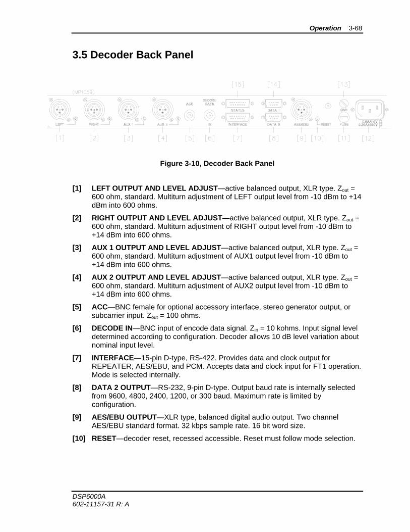
Operation 3-68
DSP6000A 602-11157-31 R: A
3.5 Decoder Back Panel
Figure 3-10, Decoder Back Panel
[1] LEFT OUTPUT AND LEVEL ADJUST—active balanced output, XLR type. Zout = 600 ohm, standard. Multiturn adjustment of LEFT output level from -10 dBm to +14 dBm into 600 ohms.
[2] RIGHT OUTPUT AND LEVEL ADJUST—active balanced output, XLR type. Zout = 600 ohm, standard. Multiturn adjustment of RIGHT output level from -10 dBm to +14 dBm into 600 ohms.
[3] AUX 1 OUTPUT AND LEVEL ADJUST—active balanced output, XLR type. Zout = 600 ohm, standard. Multiturn adjustment of AUX1 output level from -10 dBm to +14 dBm into 600 ohms.
[4] AUX 2 OUTPUT AND LEVEL ADJUST—active balanced output, XLR type. Zout = 600 ohm, standard. Multiturn adjustment of AUX2 output level from -10 dBm to +14 dBm into 600 ohms.
[5] ACC—BNC female for optional accessory interface, stereo generator output, or subcarrier input. Zout = 100 ohms.
[6] DECODE IN—BNC input of encode data signal. Zin = 10 kohms. Input signal level determined according to configuration. Decoder allows 10 dB level variation about nominal input level.
[7] INTERFACE—15-pin D-type, RS-422. Provides data and clock output for REPEATER, AES/EBU, and PCM. Accepts data and clock input for FT1 operation. Mode is selected internally.
[8] DATA 2 OUTPUT—RS-232, 9-pin D-type. Output baud rate is internally selected from 9600, 4800, 2400, 1200, or 300 baud. Maximum rate is limited by configuration.
[9] AES/EBU OUTPUT—XLR type, balanced digital audio output. Two channel AES/EBU standard format. 32 kbps sample rate. 16 bit word size.
[10] RESET—decoder reset, recessed accessible. Reset must follow mode selection.
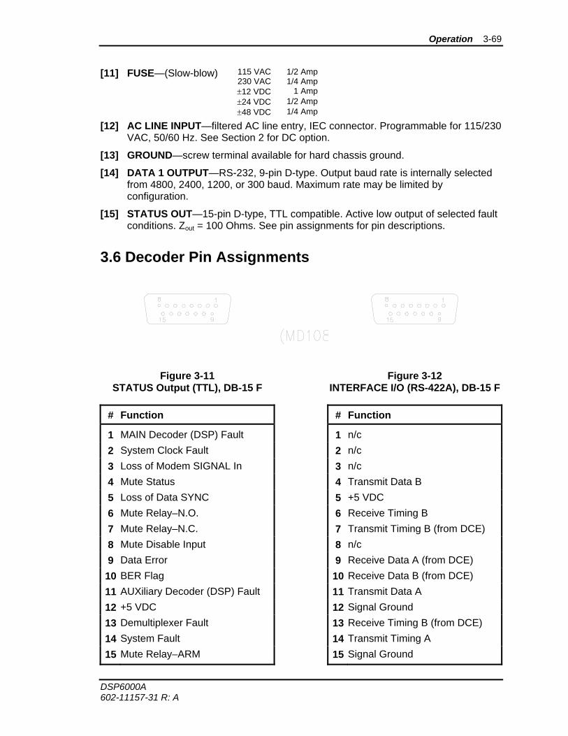
Operation 3-69
DSP6000A 602-11157-31 R: A
[11] FUSE—(Slow-blow)
115 VAC 1/2 Amp 230 VAC 1/4 Amp ±12 VDC 1 Amp ±24 VDC 1/2 Amp ±48 VDC 1/4 Amp
.
[12] AC LINE INPUT—filtered AC line entry, IEC connector. Programmable for 115/230 VAC, 50/60 Hz. See Section 2 for DC option.
[13] GROUND—screw terminal available for hard chassis ground.
[14] DATA 1 OUTPUT—RS-232, 9-pin D-type. Output baud rate is internally selected from 4800, 2400, 1200, or 300 baud. Maximum rate may be limited by configuration.
[15] STATUS OUT—15-pin D-type, TTL compatible. Active low output of selected fault conditions. Zout = 100 Ohms. See pin assignments for pin descriptions.
3.6 Decoder Pin Assignments
Figure 3-11 STATUS Output (TTL), DB-15 F
Figure 3-12 INTERFACE I/O (RS-422A), DB-15 F
# Function # Function
1 MAIN Decoder (DSP) Fault 1 n/c 2 System Clock Fault 2 n/c 3 Loss of Modem SIGNAL In 3 n/c 4 Mute Status 4 Transmit Data B 5 Loss of Data SYNC 5 +5 VDC 6 Mute Relay–N.O. 6 Receive Timing B 7 Mute Relay–N.C. 7 Transmit Timing B (from DCE) 8 Mute Disable Input 8 n/c 9 Data Error 9 Receive Data A (from DCE)
10 BER Flag 10 Receive Data B (from DCE) 11 AUXiliary Decoder (DSP) Fault 11 Transmit Data A 12 +5 VDC 12 Signal Ground 13 Demultiplexer Fault 13 Receive Timing B (from DCE) 14 System Fault 14 Transmit Timing A 15 Mute Relay–ARM 15 Signal Ground
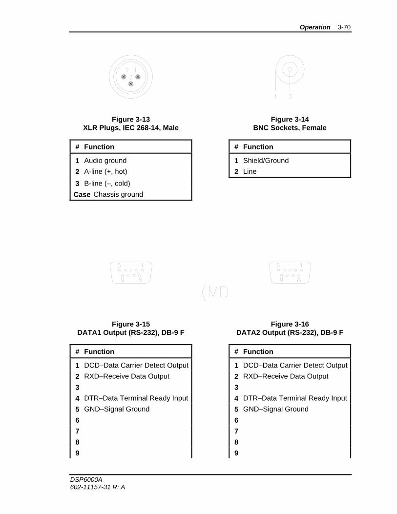
Operation 3-70
DSP6000A 602-11157-31 R: A
Figure 3-13 XLR Plugs, IEC 268-14, Male
Figure 3-14 BNC Sockets, Female
# Function # Function
1 Audio ground 1 Shield/Ground 2 A-line (+, hot) 2 Line
3 B-line (–, cold) Case Chassis ground
Figure 3-15 DATA1 Output (RS-232), DB-9 F
Figure 3-16 DATA2 Output (RS-232), DB-9 F
# Function # Function
1 DCD–Data Carrier Detect Output 1 DCD–Data Carrier Detect Output2 RXD–Receive Data Output 2 RXD–Receive Data Output 3 3 4 DTR–Data Terminal Ready Input 4 DTR–Data Terminal Ready Input5 GND–Signal Ground 5 GND–Signal Ground 6 6 7 7 8 8 9 9
Operation 3-71
DSP6000A 602-11157-31 R: A
Shell Chassis ground Shell Chassis ground
DSP6000A 602-11157-41 R: A
Section 4
Customer Service
Section Contents Page
4.1 Introduction 4-2 4.2 Technical Consultation 4-2 4.3 Factory Service 4-3 4.4 Field Repair 4-4
Customer Service 4-73
DSP6000A 602-11157-41 R: A
4.1 Introduction
Moseley Associates will assist its product users with difficulties. Most problems can be resolved through telephone consultation with our technical service department. When necessary, factory service may be provided. If you are not certain whether factory service of your equipment is covered, please check your product Warranty/Service Agreement.
Do not return any equipment to Moseley without prior consultation.
The solutions to many technical problems can be found in our product manuals; please read them and become familiar with your equipment.
We invite you to visit our Internet web site at http://www.moseleysb.com/ .
4.2 Technical Consultation
Please have the following information available prior to calling the factory:
• Model number and serial number of unit;
• Shipment date or date of purchase of an Extended Service Agreement;
• Any markings on suspected subassemblies (such as revision level); and
• Factory test data, if applicable.
Efficient resolution of your problem will be facilitated by an accurate description of the problem and its precise symptoms. For example, is the problem intermittent or constant? What are the front panel indications? If applicable, what is your operating frequency?
Technical consultation is available at (805) 968-9621 from 8:00 a.m. to 5:00 p.m., Pacific time, Monday through Friday. During these hours a technical service representative who knows your product should be available. If the representative for your product is busy, your call will be returned as soon as possible. Leave your name, station call letters if applicable, type of equipment, and telephone number(s) where you can be reached in the next few hours.
Please understand that, in trying to keep our service lines open, we may be unable to provide “walk-through” consultation. Instead, our representative will usually suggest the steps to resolve your problem; try these steps and, if your problem remains, do not hesitate to call back.
After-Hours Emergencies
Emergency consultation is available through the same telephone number from 5:00 p.m. to 10:00 p.m. Pacific time, Monday to Friday, and from 8:00 a.m. to 10:00 p.m. Pacific time on weekends and holidays. Please do not call during these hours unless you have an emergency with installed equipment. Our representative will not be able to take orders for parts, provide order status information, or assist with installation problems.
Customer Service 4-74
DSP6000A 602-11157-41 R: A
4.3 Factory Service
Arrangements for factory service should be made only with a Moseley technical service representative. You will be given a Return Authorization (RA) number. This number will expedite the routing of your equipment directly to the service department. Do not send any equipment to Moseley Associates without an RA number.
When returning equipment for troubleshooting and repair, include a detailed description of the symptoms experienced in the field, as well as any other information that well help us fix the problem and get the equipment back to you as fast as possible. Include your RA number inside the carton.
If you are shipping a complete chassis, all modules should be tied down or secured as they were originally received. On some Moseley Associates equipment, printing on the underside or topside of the chassis will indicate where shipping screws should be installed and secured.
Ship equipment in its original packing, if possible. If you are shipping a subassembly, please pack it generously to survive shipping. Make sure the carton is packed fully and evenly without voids, to prevent shifting. Seal it with appropriate shipping tape or nylon-reinforced tape. Mark the outside of the carton "Electronic Equipment - Fragile" in large red letters. Note the RA number clearly on the carton or on the shipping label, and make sure the name of your company is listed on the shipping label. Insure your shipment appropriately. All equipment must be shipped prepaid.
The survival of your equipment depends on the care you take in shipping it.
Address shipments to:
MOSELEY ASSOCIATES, INC. Attn: Technical Services Department 111 Castilian Drive Santa Barbara, CA 93117
Moseley Associates, Inc. will return the equipment prepaid under Warranty and Service Agreement conditions, and either freight collect or billed for equipment not covered by Warranty or a Service Agreement.
Customer Service 4-75
DSP6000A 602-11157-41 R: A
4.4 Field Repair
Some Moseley Associates equipment will have stickers covering certain potentiometers, varicaps, screws, and so forth. Please contact Moseley Associates technical service department before breaking these stickers. Breaking a tamperproof sticker may void your warranty.
When working with Moseley’s electronic circuits, work on a grounded antistatic surface, wear a ground strap, and use industry-standard ESD control.
Try to isolate a problem to a module or to a specific section of a module. Then compare actual wave shapes and voltage levels in your circuit with any shown on the block and level diagrams or schematics. These will sometimes allow the problem to be traced to a component.
Spare Parts Kits
Spare parts kits are available for all Moseley Associates products. We encourage the purchase of the appropriate kits to allow self-sufficiency with regard to parts. Information about spares kits for your product may be obtained from our sales department or technical service department.
Module Exchange
When it is impossible or impractical to trace a problem to the component level, replacing an entire module or subassembly may be a more expedient way to correct the problem. Replacement modules are normally available at Moseley Associates for immediate shipment. Arrange delivery of a module with our technical services representative. If the shipment is to be held at your local airport with a telephone number to call, please provide an alternate number as well. This can prevent unnecessary delays.
Customer Service 4-76
DSP6000A 602-11157-41 R: A
Field Repair Techniques
If an integrated circuit is suspect, carefully remove the original and install the new one, observing polarity. Installing an IC backward may damage not only the component itself, but the surrounding circuitry as well. IC’s occasionally exhibit temperature-sensitive characteristics. If a device operates intermittently, or appears to drift, rapidly cooling the component with a cryogenic spray may aid in identifying the problem.
If a soldered component must be replaced, do the following:
• Use a 40W maximum soldering iron with an 1/8-inch maximum tip. Do not use a soldering gun. Excessive heat can damage components and the printed circuit. Surface mount devices are especially heat sensitive, and require a lower power soldering iron. If you are not experienced with surface mount components, we suggest that you do not learn on critical equipment.
• Remove the solder from the component leads and the printed circuit pads. Solder wicking braid or a vacuum de-solderer are useful for this. Gently loosen the component leads and extract the component from the board.
• Form the leads of the replacement component to fit easily into the circuit board pattern.
• Solder each lead of the component to the bottom side of the board, using a good brand of rosin-core solder. We recommend not using water soluble flux, particularly in RF portions of the circuit. The solder should flow through the hole and form a fillet on both sides. Fillets should be smooth and shiny, but do not overheat the component trying to obtain this result.
• Trim the leads of the replacement component close to the solder on the pad side of the printed circuit board with a pair of diagonal cutters.
• Completely remove all residual flux with a cotton swab moistened with flux cleaner.
• For long term quality, inspect each solder joint—top-side and bottom—under a magnifier and rework solder joints to meet industry standards. Inspect the nearby components soldered by the Moseley Associates production line for an example of high reliability soldering.
DSP6000A 602-11157-51 R: A
Section 5
Configuration
Section Contents Page
5.1 Introduction 5-2 5.2 Encoder Channel Configuration 5-3 5.3 Encoder Alignment 5-5 5.4 Encoder Interface Configuration 5-9 5.4.1 Interface Mode 0 — PROGRAM, FT1 SEND 5-10 5.4.2 Interface Mode 1 — REPEATER 5-11 5.4.3 Interface Mode 2 — AES/EBU, FT1 SEND 5-12 5.4.4 Interface Mode 3 — PCM 5-13 5.4.5 Interface Mode 4 — PROGRAM, FT1 RECEIVE 5-14 5.4.6 Interface Mode 5 — AES/EBU, FT1 RECEIVE 5-15 5.5 Decoder Channel Configuration 5-16 5.6 Decoder Alignment 5-18 5.6.1 Decoder Alignment — Standard Efficiency 5-21 5.6.2 Decoder Alignment — High Efficiency with Pilot 5-23 5.6.3 Decoder Alignment — Standard Efficiency with Pilot 5-25 5.6.4 Decoder Alignment — FT1 5-27 5.7 Decoder Interface Configuration 5-27 5.7.1 Interface Mode 0 — PROGRAM 5-28 5.7.2 Interface Mode 1 — REPEATER 5-29 5.7.3 Interface Mode 2 — AES/EBU 5-30 5.7.4 Interface Mode 3 — PCM 5-31 5.7.5 STL Interface Mode 5-32 5.7.6 FT1 Interface Mode 5-32 5.8 Changing Transmission Efficiency 5-33 5.9 Data Channel Configuration 5-33 5.9.1 DATA 1 (RS-232) 5-35 5.9.2 DATA 2 (RS-232) 5-37 5.10 BER Threshold Selection 5-38 5.11 Automatic Audio Mute 5-39 5.12 Scrambler Disable 5-39 5.13 Configuration Programming Summary Tables 5-40

Configuration 5-78
DSP6000A 602-11157-51 R: A
5.1 Introduction
This section contains configuration and alignment procedures for the DSP6000A Encoder and Decoder. It is intended to aid the user in system reconfiguration and general troubleshooting in the field. The Encoder and Decoder are configured as specified by the customer before delivery from the factory.
For certain alignment procedures, a rough field measurement may be performed with a voltmeter instead of an oscilloscope. These cases are noted in the text.
Configuration requires the setting of DIP switches. The DSP6000A may contain different types of switches. Figure 5-1 illustrates settings for the two most common types of DIP switches.
Figure 5-1
DIP Switch Setting Definitions
Transmission Efficiency Modes
Available efficiency modes are “standard” and “high”. Standard efficiency mode may be further configured with pilot-aided recovery similar to the high efficiency mode.
Standard efficiency mode is compatible with existing DSP6000 STL and FT1 installations.
The pilot feature allows the DSP6000A to be compatible with the Moseley NX64 digital transceiver radio for repeater applications. The pilot feature is not compatible with existing DSP6000 STL and FT1 installations.
For a more detailed discussion of transmission efficiency, refer to the appendix.
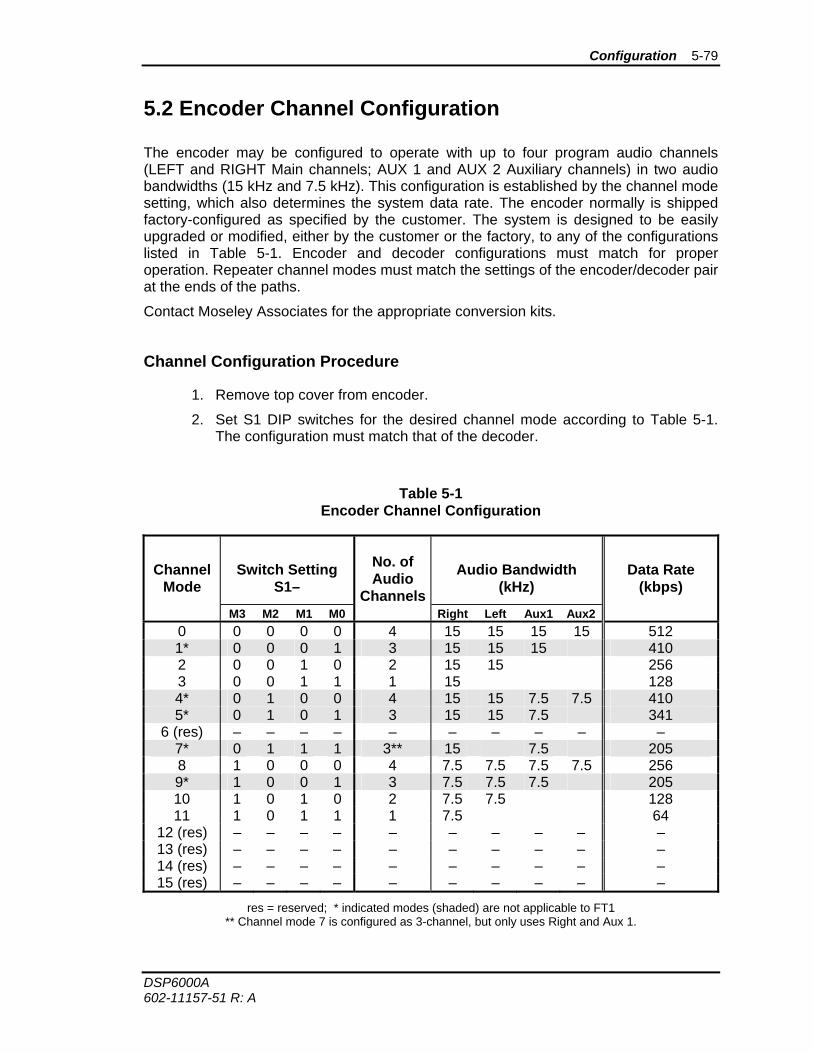
Configuration 5-79
DSP6000A 602-11157-51 R: A
5.2 Encoder Channel Configuration
The encoder may be configured to operate with up to four program audio channels (LEFT and RIGHT Main channels; AUX 1 and AUX 2 Auxiliary channels) in two audio bandwidths (15 kHz and 7.5 kHz). This configuration is established by the channel mode setting, which also determines the system data rate. The encoder normally is shipped factory-configured as specified by the customer. The system is designed to be easily upgraded or modified, either by the customer or the factory, to any of the configurations listed in Table 5-1. Encoder and decoder configurations must match for proper operation. Repeater channel modes must match the settings of the encoder/decoder pair at the ends of the paths.
Contact Moseley Associates for the appropriate conversion kits.
Channel Configuration Procedure
1. Remove top cover from encoder.
2. Set S1 DIP switches for the desired channel mode according to Table 5-1. The configuration must match that of the decoder.
Table 5-1 Encoder Channel Configuration
Channel Mode
Switch Setting S1–
No. of Audio
Channels
Audio Bandwidth (kHz)
Data Rate (kbps)
M3 M2 M1 M0 Right Left Aux1 Aux2 0 0 0 0 0 4 15 15 15 15 512 1* 0 0 0 1 3 15 15 15 410 2 0 0 1 0 2 15 15 256 3 0 0 1 1 1 15 128 4* 0 1 0 0 4 15 15 7.5 7.5 410 5* 0 1 0 1 3 15 15 7.5 341
6 (res) – – – – – – – – – – 7* 0 1 1 1 3** 15 7.5 205 8 1 0 0 0 4 7.5 7.5 7.5 7.5 256 9* 1 0 0 1 3 7.5 7.5 7.5 205 10 1 0 1 0 2 7.5 7.5 128 11 1 0 1 1 1 7.5 64
12 (res) – – – – – – – – – – 13 (res) – – – – – – – – – – 14 (res) – – – – – – – – – – 15 (res) – – – – – – – – – –
res = reserved; * indicated modes (shaded) are not applicable to FT1 ** Channel mode 7 is configured as 3-channel, but only uses Right and Aux 1.
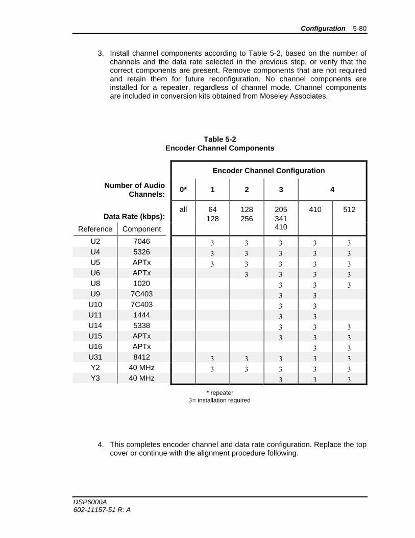
Configuration 5-80
DSP6000A 602-11157-51 R: A
3. Install channel components according to Table 5-2, based on the number of channels and the data rate selected in the previous step, or verify that the correct components are present. Remove components that are not required and retain them for future reconfiguration. No channel components are installed for a repeater, regardless of channel mode. Channel components are included in conversion kits obtained from Moseley Associates.
Table 5-2 Encoder Channel Components
Encoder Channel Configuration
Number of Audio Channels: 0* 1 2 3 4
Data Rate (kbps):
all 64 128
128 256
205 341
410 512
Reference Component 410
U2 7046 3 3 3 3 3 U4 5326 3 3 3 3 3 U5 APTx 3 3 3 3 3 U6 APTx 3 3 3 3 U8 1020 3 3 3 U9 7C403 3 3
U10 7C403 3 3 U11 1444 3 3 U14 5338 3 3 3 U15 APTx 3 3 3 U16 APTx 3 3 U31 8412 3 3 3 3 3 Y2 40 MHz 3 3 3 3 3 Y3 40 MHz 3 3 3
* repeater 3= installation required
4. This completes encoder channel and data rate configuration. Replace the top cover or continue with the alignment procedure following.
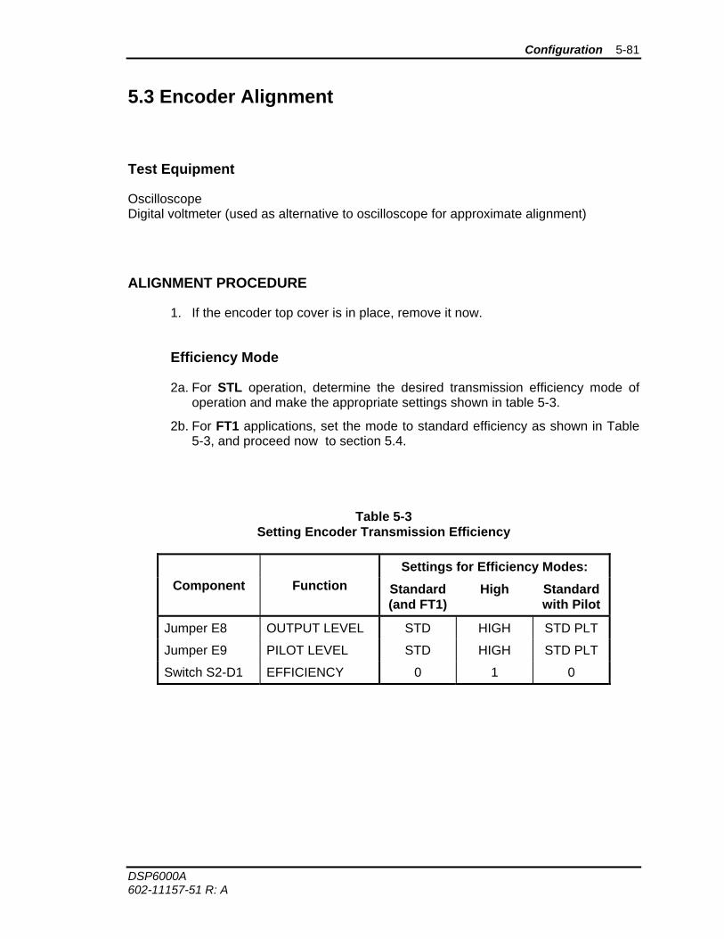
Configuration 5-81
DSP6000A 602-11157-51 R: A
5.3 Encoder Alignment
Test Equipment
Oscilloscope Digital voltmeter (used as alternative to oscilloscope for approximate alignment)
ALIGNMENT PROCEDURE
1. If the encoder top cover is in place, remove it now.
Efficiency Mode
2a. For STL operation, determine the desired transmission efficiency mode of operation and make the appropriate settings shown in table 5-3.
2b. For FT1 applications, set the mode to standard efficiency as shown in Table 5-3, and proceed now to section 5.4.
Table 5-3 Setting Encoder Transmission Efficiency
Settings for Efficiency Modes: Component Function Standard
(and FT1) High Standard
with Pilot
Jumper E8 OUTPUT LEVEL STD HIGH STD PLT
Jumper E9 PILOT LEVEL STD HIGH STD PLT
Switch S2-D1 EFFICIENCY 0 1 0
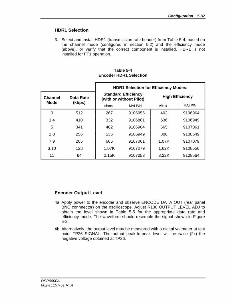
Configuration 5-82
DSP6000A 602-11157-51 R: A
HDR1 Selection
3. Select and install HDR1 (transmission rate header) from Table 5-4, based on the channel mode (configured in section 5.2) and the efficiency mode (above), or verify that the correct component is installed. HDR1 is not installed for FT1 operation.
Table 5-4 Encoder HDR1 Selection
HDR1 Selection for Efficiency Modes:
Channel Mode
Data Rate (kbps)
Standard Efficiency (with or without Pilot)
ohms MAI P/N
High Efficiency
ohms MAI P/N
0 512 267 9106956 402 9106964
1,4 410 332 9106881 536 9106949
5 341 402 9106964 665 9107061
2,8 256 536 9106949 806 9108549
7,9 205 665 9107061 1.07K 9107079
3,10 128 1.07K 9107079 1.62K 9108556
11 64 2.15K 9107053 3.32K 9108564
Encoder Output Level
4a. Apply power to the encoder and observe ENCODE DATA OUT (rear panel BNC connnector) on the oscilloscope. Adjust R138 OUTPUT LEVEL ADJ to obtain the level shown in Table 5-5 for the appropriate data rate and efficiency mode. The waveform should resemble the signal shown in Figure 5-2.
4b. Alternatively, the output level may be measured with a digital voltmeter at test point TP26 SIGNAL. The output peak-to-peak level will be twice (2x) the negative voltage obtained at TP26.
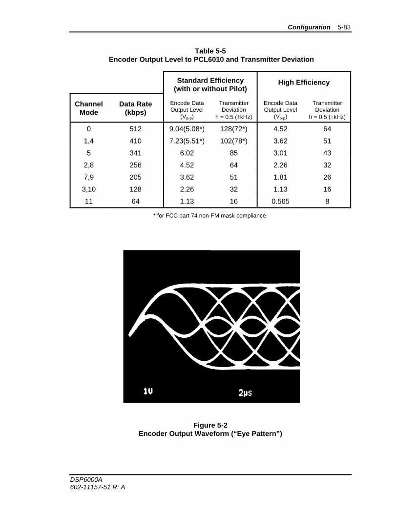
Configuration 5-83
DSP6000A 602-11157-51 R: A
Table 5-5 Encoder Output Level to PCL6010 and Transmitter Deviation
Standard Efficiency (with or without Pilot)
High Efficiency
Channel Mode
Data Rate (kbps)
Encode Data Output Level
(Vp-p)
Transmitter Deviation
h = 0.5 (±kHz)
Encode Data Output Level
(Vp-p)
Transmitter Deviation
h = 0.5 (±kHz)
0 512 9.04(5.08*) 128(72*) 4.52 64
1,4 410 7.23(5.51*) 102(78*) 3.62 51
5 341 6.02 85 3.01 43
2,8 256 4.52 64 2.26 32
7,9 205 3.62 51 1.81 26
3,10 128 2.26 32 1.13 16
11 64 1.13 16 0.565 8
* for FCC part 74 non-FM mask compliance.
Figure 5-2 Encoder Output Waveform (“Eye Pattern”)
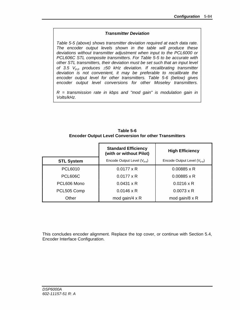
Configuration 5-84
DSP6000A 602-11157-51 R: A
Transmitter Deviation
Table 5-5 (above) shows transmitter deviation required at each data rate. The encoder output levels shown in the table will produce these deviations without transmitter adjustment when input to the PCL6000 or PCL606C STL composite transmitters. For Table 5-5 to be accurate with other STL transmitters, their deviation must be set such that an input level of 3.5 Vp-p produces ±50 kHz deviation. If recalibrating transmitter deviation is not convenient, it may be preferable to recalibrate the encoder output level for other transmitters. Table 5-6 (below) gives encoder output level conversions for other Moseley transmitters. R = transmission rate in kbps and "mod gain" is modulation gain in Volts/kHz.
Table 5-6 Encoder Output Level Conversion for other Transmitters
Standard Efficiency
(with or without Pilot) High Efficiency
STL System Encode Output Level (Vp-p) Encode Output Level (Vp-p)
PCL6010 0.0177 x R 0.00885 x R
PCL606C 0.0177 x R 0.00885 x R
PCL606 Mono 0.0431 x R 0.0216 x R
PCL505 Comp 0.0146 x R 0.0073 x R
Other mod gain/4 x R mod gain/8 x R
This concludes encoder alignment. Replace the top cover, or continue with Section 5.4, Encoder Interface Configuration.
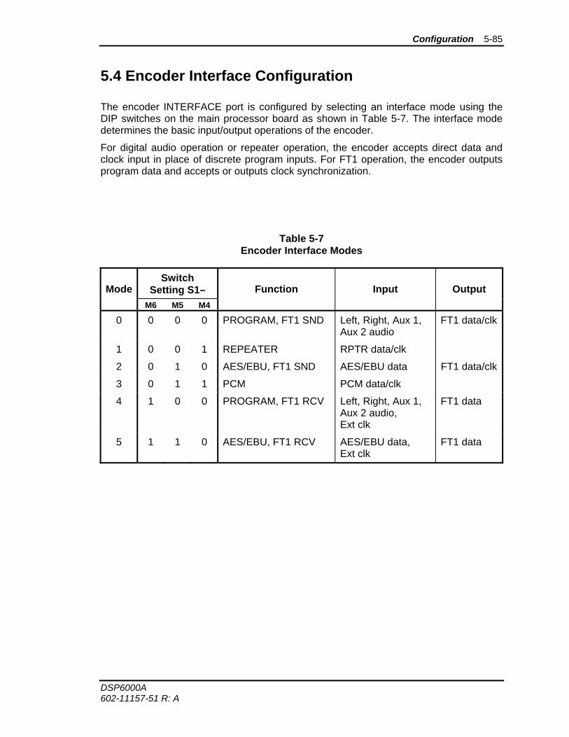
Configuration 5-85
DSP6000A 602-11157-51 R: A
5.4 Encoder Interface Configuration
The encoder INTERFACE port is configured by selecting an interface mode using the DIP switches on the main processor board as shown in Table 5-7. The interface mode determines the basic input/output operations of the encoder.
For digital audio operation or repeater operation, the encoder accepts direct data and clock input in place of discrete program inputs. For FT1 operation, the encoder outputs program data and accepts or outputs clock synchronization.
Table 5-7 Encoder Interface Modes
Mode Switch
Setting S1– Function Input Output M6 M5 M4
0 0 0 0 PROGRAM, FT1 SND Left, Right, Aux 1, Aux 2 audio
FT1 data/clk
1 0 0 1 REPEATER RPTR data/clk
2 0 1 0 AES/EBU, FT1 SND AES/EBU data FT1 data/clk
3 0 1 1 PCM PCM data/clk
4 1 0 0 PROGRAM, FT1 RCV Left, Right, Aux 1, Aux 2 audio, Ext clk
FT1 data
5 1 1 0 AES/EBU, FT1 RCV AES/EBU data, Ext clk
FT1 data
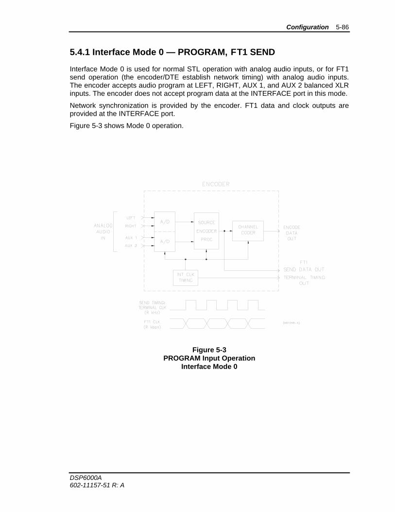
Configuration 5-86
DSP6000A 602-11157-51 R: A
5.4.1 Interface Mode 0 — PROGRAM, FT1 SEND
Interface Mode 0 is used for normal STL operation with analog audio inputs, or for FT1 send operation (the encoder/DTE establish network timing) with analog audio inputs. The encoder accepts audio program at LEFT, RIGHT, AUX 1, and AUX 2 balanced XLR inputs. The encoder does not accept program data at the INTERFACE port in this mode.
Network synchronization is provided by the encoder. FT1 data and clock outputs are provided at the INTERFACE port.
Figure 5-3 shows Mode 0 operation.
Figure 5-3 PROGRAM Input Operation
Interface Mode 0
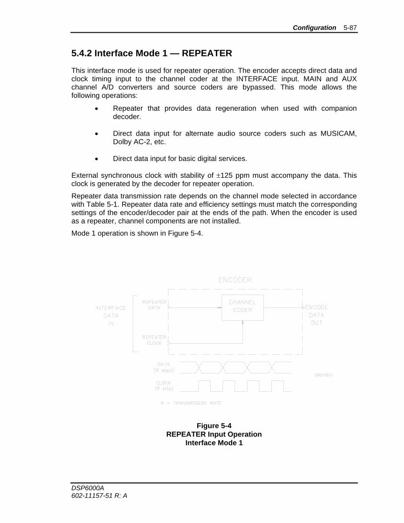
Configuration 5-87
DSP6000A 602-11157-51 R: A
5.4.2 Interface Mode 1 — REPEATER
This interface mode is used for repeater operation. The encoder accepts direct data and clock timing input to the channel coder at the INTERFACE input. MAIN and AUX channel A/D converters and source coders are bypassed. This mode allows the following operations:
• Repeater that provides data regeneration when used with companion decoder.
• Direct data input for alternate audio source coders such as MUSICAM, Dolby AC-2, etc.
• Direct data input for basic digital services.
External synchronous clock with stability of ±125 ppm must accompany the data. This clock is generated by the decoder for repeater operation.
Repeater data transmission rate depends on the channel mode selected in accordance with Table 5-1. Repeater data rate and efficiency settings must match the corresponding settings of the encoder/decoder pair at the ends of the path. When the encoder is used as a repeater, channel components are not installed.
Mode 1 operation is shown in Figure 5-4.
Figure 5-4 REPEATER Input Operation
Interface Mode 1
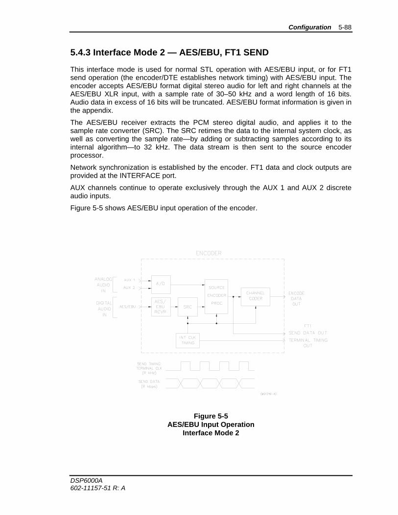
Configuration 5-88
DSP6000A 602-11157-51 R: A
5.4.3 Interface Mode 2 — AES/EBU, FT1 SEND
This interface mode is used for normal STL operation with AES/EBU input, or for FT1 send operation (the encoder/DTE establishes network timing) with AES/EBU input. The encoder accepts AES/EBU format digital stereo audio for left and right channels at the AES/EBU XLR input, with a sample rate of 30–50 kHz and a word length of 16 bits. Audio data in excess of 16 bits will be truncated. AES/EBU format information is given in the appendix.
The AES/EBU receiver extracts the PCM stereo digital audio, and applies it to the sample rate converter (SRC). The SRC retimes the data to the internal system clock, as well as converting the sample rate—by adding or subtracting samples according to its internal algorithm—to 32 kHz. The data stream is then sent to the source encoder processor.
Network synchronization is established by the encoder. FT1 data and clock outputs are provided at the INTERFACE port.
AUX channels continue to operate exclusively through the AUX 1 and AUX 2 discrete audio inputs.
Figure 5-5 shows AES/EBU input operation of the encoder.
Figure 5-5 AES/EBU Input Operation
Interface Mode 2
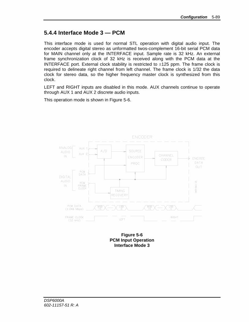
Configuration 5-89
DSP6000A 602-11157-51 R: A
5.4.4 Interface Mode 3 — PCM
This interface mode is used for normal STL operation with digital audio input. The encoder accepts digital stereo as unformatted twos-complement 16-bit serial PCM data for MAIN channel only at the INTERFACE input. Sample rate is 32 kHz. An external frame synchronization clock of 32 kHz is received along with the PCM data at the INTERFACE port. External clock stability is restricted to ±125 ppm. The frame clock is required to delineate right channel from left channel. The frame clock is 1/32 the data clock for stereo data, so the higher frequency master clock is synthesized from this clock.
LEFT and RIGHT inputs are disabled in this mode. AUX channels continue to operate through AUX 1 and AUX 2 discrete audio inputs.
This operation mode is shown in Figure 5-6.
Figure 5-6 PCM Input Operation
Interface Mode 3
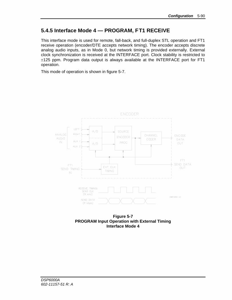
Configuration 5-90
DSP6000A 602-11157-51 R: A
5.4.5 Interface Mode 4 — PROGRAM, FT1 RECEIVE
This interface mode is used for remote, fall-back, and full-duplex STL operation and FT1 receive operation (encoder/DTE accepts network timing). The encoder accepts discrete analog audio inputs, as in Mode 0, but network timing is provided externally. External clock synchronization is received at the INTERFACE port. Clock stability is restricted to ±125 ppm. Program data output is always available at the INTERFACE port for FT1 operation.
This mode of operation is shown in figure 5-7.
Figure 5-7 PROGRAM Input Operation with External Timing
Interface Mode 4
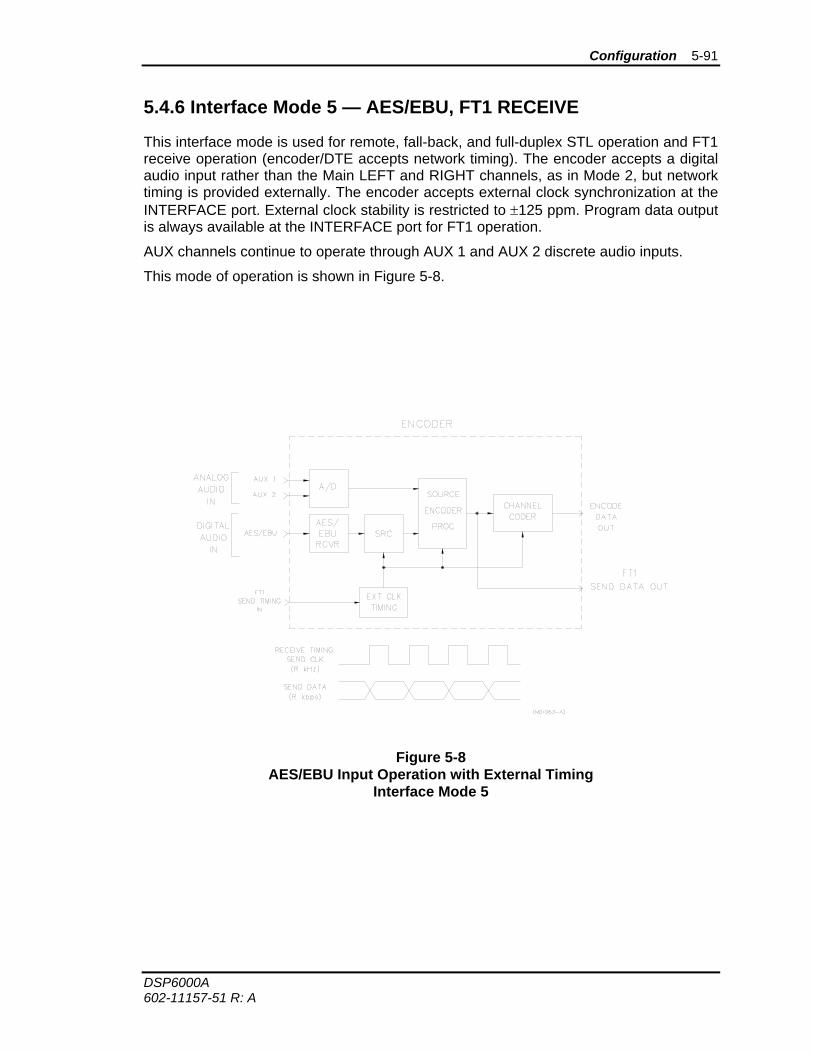
Configuration 5-91
DSP6000A 602-11157-51 R: A
5.4.6 Interface Mode 5 — AES/EBU, FT1 RECEIVE
This interface mode is used for remote, fall-back, and full-duplex STL operation and FT1 receive operation (encoder/DTE accepts network timing). The encoder accepts a digital audio input rather than the Main LEFT and RIGHT channels, as in Mode 2, but network timing is provided externally. The encoder accepts external clock synchronization at the INTERFACE port. External clock stability is restricted to ±125 ppm. Program data output is always available at the INTERFACE port for FT1 operation.
AUX channels continue to operate through AUX 1 and AUX 2 discrete audio inputs.
This mode of operation is shown in Figure 5-8.
Figure 5-8 AES/EBU Input Operation with External Timing
Interface Mode 5
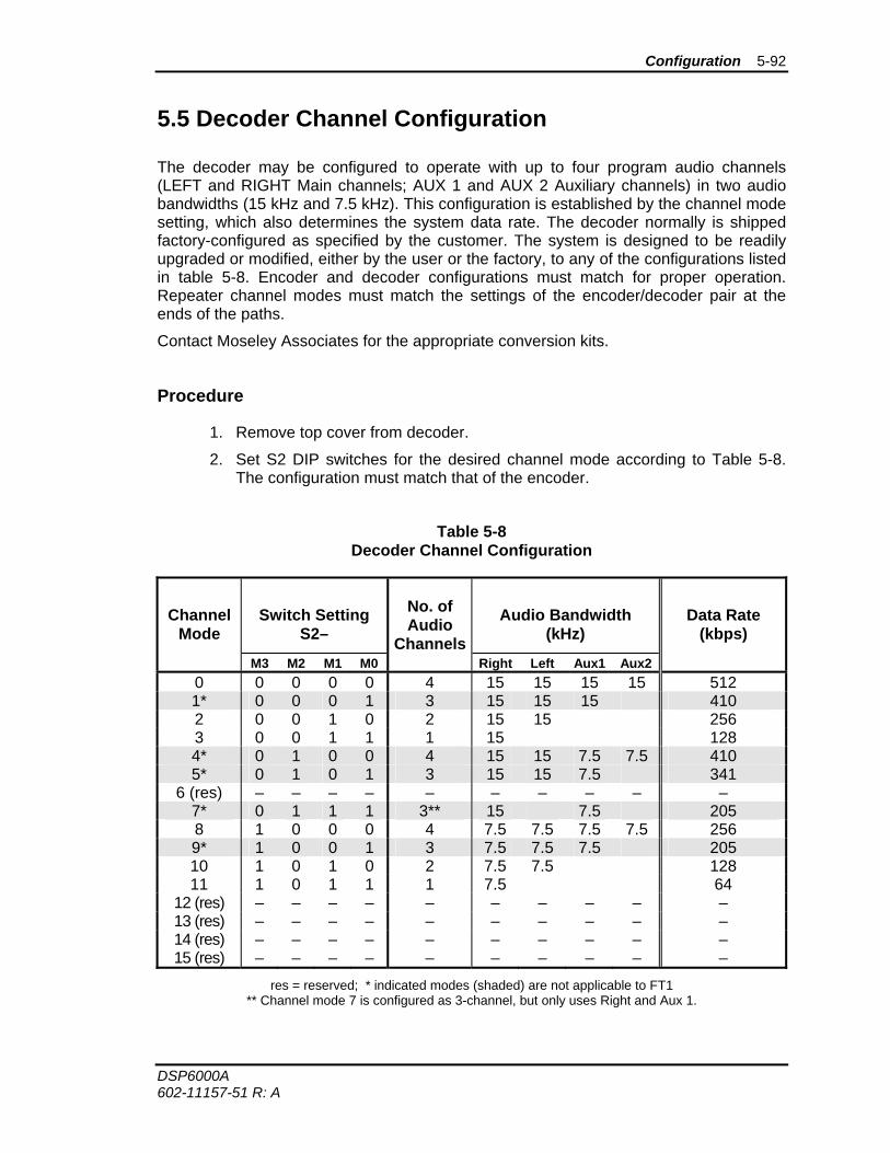
Configuration 5-92
DSP6000A 602-11157-51 R: A
5.5 Decoder Channel Configuration
The decoder may be configured to operate with up to four program audio channels (LEFT and RIGHT Main channels; AUX 1 and AUX 2 Auxiliary channels) in two audio bandwidths (15 kHz and 7.5 kHz). This configuration is established by the channel mode setting, which also determines the system data rate. The decoder normally is shipped factory-configured as specified by the customer. The system is designed to be readily upgraded or modified, either by the user or the factory, to any of the configurations listed in table 5-8. Encoder and decoder configurations must match for proper operation. Repeater channel modes must match the settings of the encoder/decoder pair at the ends of the paths.
Contact Moseley Associates for the appropriate conversion kits.
Procedure
1. Remove top cover from decoder.
2. Set S2 DIP switches for the desired channel mode according to Table 5-8. The configuration must match that of the encoder.
Table 5-8 Decoder Channel Configuration
Channel Mode
Switch Setting S2–
No. of Audio
Channels
Audio Bandwidth (kHz)
Data Rate (kbps)
M3 M2 M1 M0 Right Left Aux1 Aux2 0 0 0 0 0 4 15 15 15 15 512 1* 0 0 0 1 3 15 15 15 410 2 0 0 1 0 2 15 15 256 3 0 0 1 1 1 15 128 4* 0 1 0 0 4 15 15 7.5 7.5 410 5* 0 1 0 1 3 15 15 7.5 341
6 (res) – – – – – – – – – – 7* 0 1 1 1 3** 15 7.5 205 8 1 0 0 0 4 7.5 7.5 7.5 7.5 256 9* 1 0 0 1 3 7.5 7.5 7.5 205 10 1 0 1 0 2 7.5 7.5 128 11 1 0 1 1 1 7.5 64
12 (res) – – – – – – – – – – 13 (res) – – – – – – – – – – 14 (res) – – – – – – – – – – 15 (res) – – – – – – – – – –
res = reserved; * indicated modes (shaded) are not applicable to FT1 ** Channel mode 7 is configured as 3-channel, but only uses Right and Aux 1.
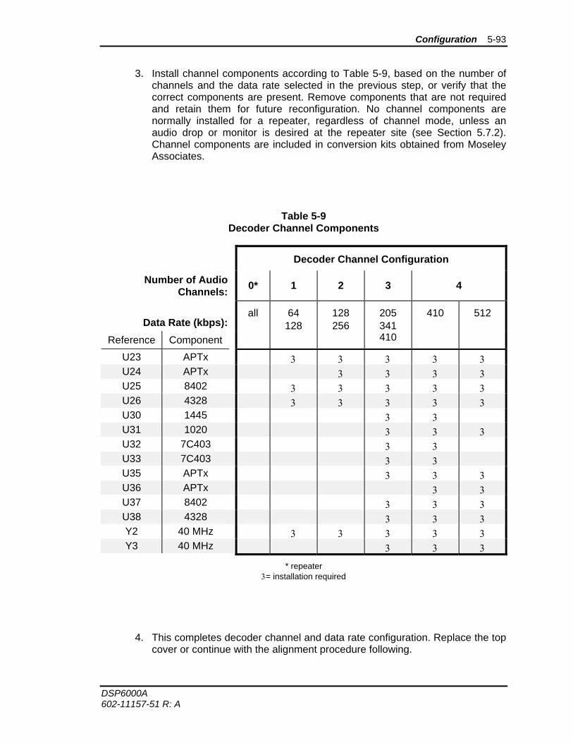
Configuration 5-93
DSP6000A 602-11157-51 R: A
3. Install channel components according to Table 5-9, based on the number of channels and the data rate selected in the previous step, or verify that the correct components are present. Remove components that are not required and retain them for future reconfiguration. No channel components are normally installed for a repeater, regardless of channel mode, unless an audio drop or monitor is desired at the repeater site (see Section 5.7.2). Channel components are included in conversion kits obtained from Moseley Associates.
Table 5-9 Decoder Channel Components
Decoder Channel Configuration
Number of Audio Channels: 0* 1 2 3 4
Data Rate (kbps):
all 64 128
128 256
205 341
410 512
Reference Component 410
U23 APTx 3 3 3 3 3 U24 APTx 3 3 3 3 U25 8402 3 3 3 3 3 U26 4328 3 3 3 3 3 U30 1445 3 3 U31 1020 3 3 3 U32 7C403 3 3 U33 7C403 3 3 U35 APTx 3 3 3 U36 APTx 3 3 U37 8402 3 3 3 U38 4328 3 3 3 Y2 40 MHz 3 3 3 3 3 Y3 40 MHz 3 3 3
* repeater 3= installation required
4. This completes decoder channel and data rate configuration. Replace the top cover or continue with the alignment procedure following.
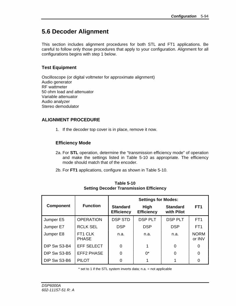
Configuration 5-94
DSP6000A 602-11157-51 R: A
5.6 Decoder Alignment
This section includes alignment procedures for both STL and FT1 applications. Be careful to follow only those procedures that apply to your configuration. Alignment for all configurations begins with step 1 below.
Test Equipment
Oscilloscope (or digital voltmeter for approximate alignment) Audio generator RF wattmeter 50 ohm load and attenuator Variable attenuator Audio analyzer Stereo demodulator
ALIGNMENT PROCEDURE
1. If the decoder top cover is in place, remove it now.
Efficiency Mode
2a. For STL operation, determine the “transmission efficiency mode” of operation and make the settings listed in Table 5-10 as appropriate. The efficiency mode should match that of the encoder.
2b. For FT1 applications, configure as shown in Table 5-10.
Table 5-10 Setting Decoder Transmission Efficiency
Settings for Modes: Component Function Standard
Efficiency High
Efficiency Standard with Pilot
FT1
Jumper E5 OPERATION DSP STD DSP PLT DSP PLT FT1
Jumper E7 RCLK SEL DSP DSP DSP FT1
Jumper E8 FT1 CLK PHASE
n.a. n.a. n.a. NORM or INV
DIP Sw S3-B4 EFF SELECT 0 1 0 0
DIP Sw S3-B5 EFF2 PHASE 0 0* 0 0
DIP Sw S3-B6 PILOT 0 1 1 0
* set to 1 if the STL system inverts data; n.a. = not applicable
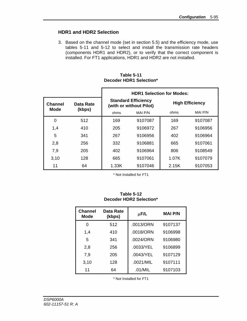
Configuration 5-95
DSP6000A 602-11157-51 R: A
HDR1 and HDR2 Selection
3. Based on the channel mode (set in section 5.5) and the efficiency mode, use tables 5-11 and 5-12 to select and install the transmission rate headers (components HDR1 and HDR2), or to verify that the correct component is installed. For FT1 applications, HDR1 and HDR2 are not installed.
Table 5-11 Decoder HDR1 Selection*
HDR1 Selection for Modes:
Channel Mode
Data Rate (kbps)
Standard Efficiency (with or without Pilot)
ohms MAI P/N
High Efficiency
ohms MAI P/N
0 512 169 9107087 169 9107087
1,4 410 205 9106972 267 9106956
5 341 267 9106956 402 9106964
2,8 256 332 9106881 665 9107061
7,9 205 402 9106964 806 9108549
3,10 128 665 9107061 1.07K 9107079
11 64 1.33K 9107046 2.15K 9107053
* Not Installed for FT1
Table 5-12 Decoder HDR2 Selection*
Channel Mode
Data Rate (kbps) μF/L MAI P/N
0 512 .0013/ORN 9107137
1,4 410 .0018/ORN 9106998
5 341 .0024/ORN 9106980
2,8 256 .0033/YEL 9106899
7,9 205 .0043/YEL 9107129
3,10 128 .0021/MIL 9107111
11 64 .01/MIL 9107103
* Not Installed for FT1
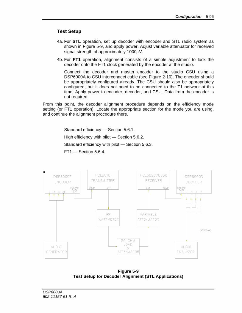
Configuration 5-96
DSP6000A 602-11157-51 R: A
Test Setup
4a. For STL operation, set up decoder with encoder and STL radio system as shown in Figure 5-9, and apply power. Adjust variable attenuator for received signal strength of approximately 1000μV.
4b. For FT1 operation, alignment consists of a simple adjustment to lock the decoder onto the FT1 clock generated by the encoder at the studio.
Connect the decoder and master encoder to the studio CSU using a DSP6000A to CSU interconnect cable (see Figure 2-10). The encoder should be appropriately configured already. The CSU should also be appropriately configured, but it does not need to be connected to the T1 network at this time. Apply power to encoder, decoder, and CSU. Data from the encoder is not required.
From this point, the decoder alignment procedure depends on the efficiency mode setting (or FT1 operation). Locate the appropriate section for the mode you are using, and continue the alignment procedure there.
Standard efficiency — Section 5.6.1.
High efficiency with pilot — Section 5.6.2.
Standard efficiency with pilot — Section 5.6.3.
FT1 — Section 5.6.4.
u
Figure 5-9 Test Setup for Decoder Alignment (STL Applications)
Configuration 5-97
DSP6000A 602-11157-51 R: A
5.6.1 Decoder Alignment — Standard Efficiency
Continued from section 5.6.
Decoder input level
5. Connect oscilloscope probe to TP1 FILTERED INPUT. Verify the level agrees with Table 5-13. If the level does not agree approximately with the table, check the following for proper calibration: (1) encoder output level, (2) transmitter deviation, and (3) receiver output level.
Table 5-13 Decoder Input Level — Standard Efficiency
Channel Mode
Transmission Rate, R (kbps)
Input Level (Vp-p)
0 512 9.04 (5.08*)
1,4 410 7.23 (5.51*)
5 341 6.02
2,8 256 4.52
7,9 205 3.62
3,10 128 2.26
11 64 1.13
* for FCC part 74 non-FM mask compliance.
Set AGC
6. Set S1 AGC MODE to AGC. Connect scope probe to TP4 A/D IN. Adjust R42 AGC LEVEL ADJ for level at TP4 A/D IN = 1.6 Vp-p.
Set clock recovery
7a. Connect CH1 scope probe to TP10 RCLK SIG IN. Connect CH2 scope probe to TP11 RCLK SYM. Adjust L1 on HDR2 (RCLK LVL ADJ) for peak waveform level on CH1 (TP10). The DC level at TP10 is about 3 VDC.
7b. Alternatively, adjust L1 for peak voltage on TP9 RCLK SIG LVL, using a DVM.
1. Adjust R60 RCLK SYMMETRY ADJ for waveform symmetry (50% duty cycle) on CH2 (TP11). The waveforms should correspond to Figure 5-10.
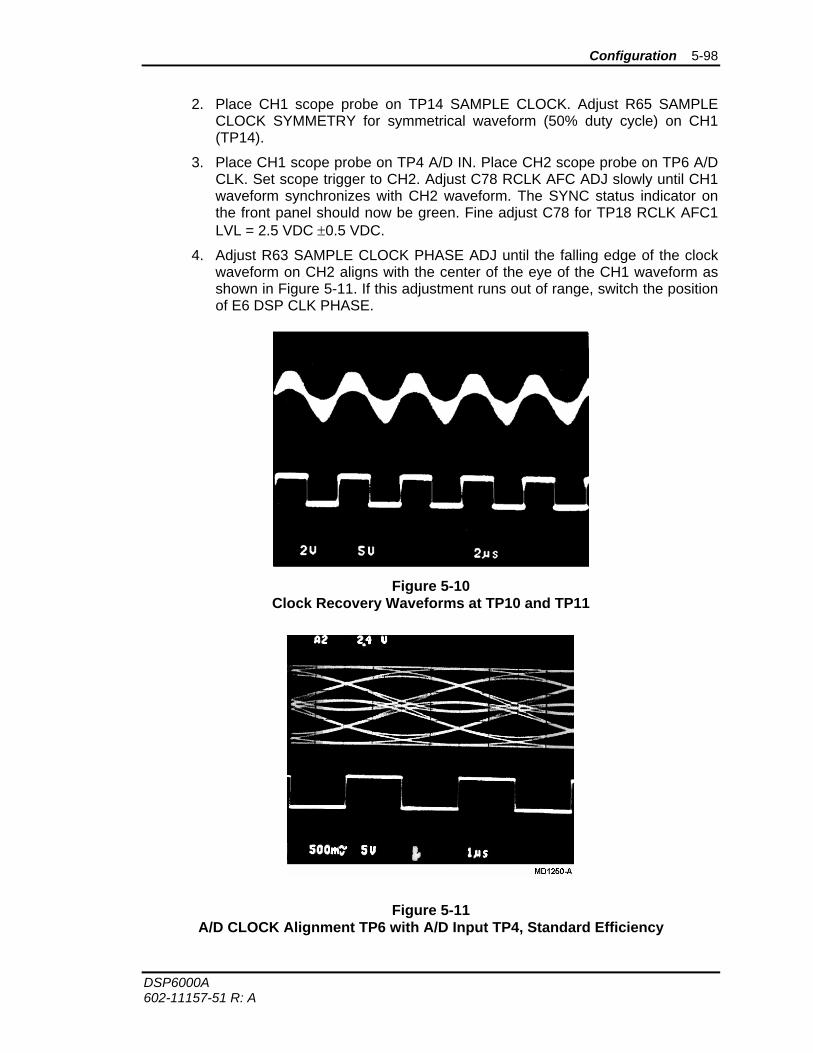
Configuration 5-98
DSP6000A 602-11157-51 R: A
2. Place CH1 scope probe on TP14 SAMPLE CLOCK. Adjust R65 SAMPLE CLOCK SYMMETRY for symmetrical waveform (50% duty cycle) on CH1 (TP14).
3. Place CH1 scope probe on TP4 A/D IN. Place CH2 scope probe on TP6 A/D CLK. Set scope trigger to CH2. Adjust C78 RCLK AFC ADJ slowly until CH1 waveform synchronizes with CH2 waveform. The SYNC status indicator on the front panel should now be green. Fine adjust C78 for TP18 RCLK AFC1 LVL = 2.5 VDC ±0.5 VDC.
4. Adjust R63 SAMPLE CLOCK PHASE ADJ until the falling edge of the clock waveform on CH2 aligns with the center of the eye of the CH1 waveform as shown in Figure 5-11. If this adjustment runs out of range, switch the position of E6 DSP CLK PHASE.
Figure 5-10
Clock Recovery Waveforms at TP10 and TP11
Figure 5-11 A/D CLOCK Alignment TP6 with A/D Input TP4, Standard Efficiency
Configuration 5-99
DSP6000A 602-11157-51 R: A
Set threshold performance
12. Increase attenuation between STL transmitter and STL receiver until data errors are indicated on decoder front panel.
13. Slowly adjust R42 AGC LEVEL ADJ to minimize data error indications. It may be necessary to increase attenuation to observe errors as optimal adjustment is reached.
14. Slowly adjust R63 SAMPLE CLOCK PHASE ADJ to minimize data error indications.
This concludes the decoder alignment for standard efficiency. Replace the cover or continue with Section 5.7, Decoder Interface Configuration.
5.6.2 Decoder Alignment — High Efficiency with Pilot
Continued from section 5.6.
Decoder input level
5. Connect oscilloscope probe to TP1 FILTERED INPUT. Verify that the input level agrees with Table 5-14 below. If this level does not approximately agree with the table, check the following for proper calibration: (1) encoder output level, (2) transmitter deviation, and (3) receiver output level.
Table 5-14 Decoder Input Level — High Efficiency
Channel Mode
Transmission Rate, R (kbps)
Input Level (Vp-p)
0 512 4.52
1,4 410 3.62
5 341 3.01
2,8 256 2.26
7,9 205 1.81
3,10 128 1.13
11 64 0.565
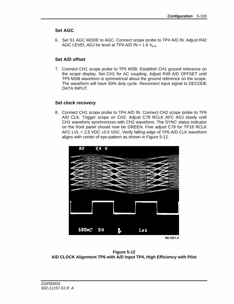
Configuration 5-100
DSP6000A 602-11157-51 R: A
Set AGC
6. Set S1 AGC MODE to AGC. Connect scope probe to TP4 A/D IN. Adjust R42 AGC LEVEL ADJ for level at TP4 A/D IN = 1.6 Vp-p.
Set A/D offset
7. Connect CH1 scope probe to TP5 MSB. Establish CH1 ground reference on the scope display. Set CH1 for AC coupling. Adjust R49 A/D OFFSET until TP5 MSB waveform is symmetrical about the ground reference on the scope. The waveform will have 50% duty cycle. Reconnect input signal to DECODE DATA INPUT.
Set clock recovery
8. Connect CH1 scope probe to TP4 A/D IN. Connect CH2 scope probe to TP6 A/D CLK. Trigger scope on CH2. Adjust C78 RCLK AFC ADJ slowly until CH1 waveform synchronizes with CH2 waveform. The SYNC status indicator on the front panel should now be GREEN. Fine adjust C78 for TP18 RCLK AFC LVL = 2.5 VDC ±0.5 VDC. Verify falling edge of TP6 A/D CLK waveform aligns with center of eye-pattern as shown in Figure 5-12.
Figure 5-12 A/D CLOCK Alignment TP6 with A/D Input TP4, High Efficiency with Pilot
Configuration 5-101
DSP6000A 602-11157-51 R: A
9. If FAULT indication is still displayed on the front panel, it is possible the data phase has been inverted by the radio. To remedy this, change DIP switch S3-B5 EFF2_PHASE to invert data phase.
Set threshold performance
10. Increase attenuation between STL transmitter and STL receiver until data errors are indicated on decoder front panel.
11. Slowly adjust R42 AGC LEVEL ADJ to minimize data error indications. It may be necessary to increase attenuation to observe errors as optimal adjustment is reached.
12. Slowly adjust R63 SAMPLE CLOCK PHASE ADJ to minimize data error indications.
This concludes the decoder alignment for high efficiency. Replace the cover or continue with Section 5.7, Decoder Interface Configuration.
5.6.3 Decoder Alignment — Standard Efficiency with Pilot
Continued from section 5.6.
Decoder input level
5. Connect scope probe to TP1 FILTERED INPUT. Verify that the input level agrees with Table 5-13 (see Section 5.6.1). If this level does not approximately agree with the table, check the following for proper calibration: (1) encoder output level, (2) transmitter deviation, and (3) receiver output level.
Set AGC
6. Set S1 AGC MODE to AGC. Connect scope probe to TP4 A/D IN. Adjust R42 AGC LEVEL ADJ for level at TP4 A/D IN = 1.55 Vp-p.
Set A/D offset
7. Connect CH1 scope probe to TP5 MSB. Establish CH1 ground reference on the scope display. Set CH1 for AC coupling. Adjust R49 A/D OFFSET until TP5 MSB waveform is symmetrical about the ground reference on the scope. The waveform will have 50% duty cycle. Reconnect input signal to DECODE DATA INPUT.
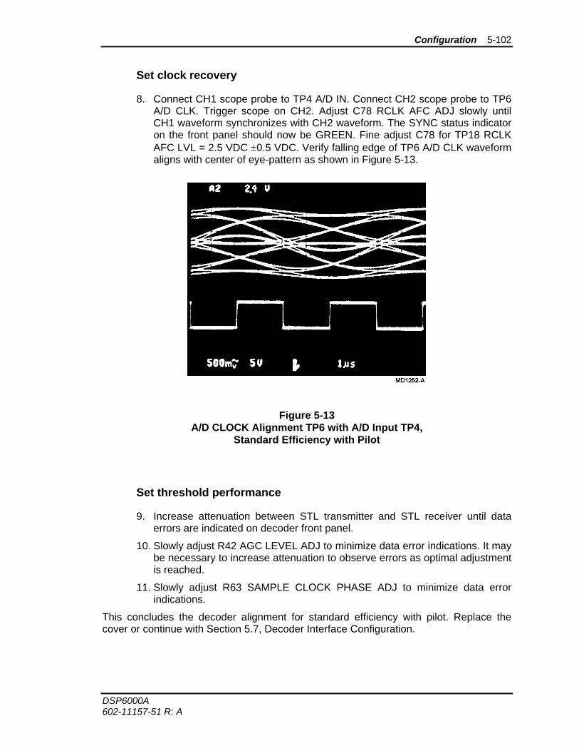
Configuration 5-102
DSP6000A 602-11157-51 R: A
Set clock recovery
8. Connect CH1 scope probe to TP4 A/D IN. Connect CH2 scope probe to TP6 A/D CLK. Trigger scope on CH2. Adjust C78 RCLK AFC ADJ slowly until CH1 waveform synchronizes with CH2 waveform. The SYNC status indicator on the front panel should now be GREEN. Fine adjust C78 for TP18 RCLK AFC LVL = 2.5 VDC ±0.5 VDC. Verify falling edge of TP6 A/D CLK waveform aligns with center of eye-pattern as shown in Figure 5-13.
Figure 5-13 A/D CLOCK Alignment TP6 with A/D Input TP4,
Standard Efficiency with Pilot
Set threshold performance
9. Increase attenuation between STL transmitter and STL receiver until data errors are indicated on decoder front panel.
10. Slowly adjust R42 AGC LEVEL ADJ to minimize data error indications. It may be necessary to increase attenuation to observe errors as optimal adjustment is reached.
11. Slowly adjust R63 SAMPLE CLOCK PHASE ADJ to minimize data error indications.
This concludes the decoder alignment for standard efficiency with pilot. Replace the cover or continue with Section 5.7, Decoder Interface Configuration.
Configuration 5-103
DSP6000A 602-11157-51 R: A
5.6.4 Decoder Alignment — FT1
Continued from section 5.6.
Set FT1 clock locking
5. Using an oscilloscope or digital voltmeter, monitor TP18 RCLK AFC 2 and adjust C78 RCLK AFC ADJ to obtain 2.5 VDC ±0.5 VDC. If you run out of room on C78, change the position of E8 FT1 CLK PHASE from NORM to INV (or vice versa) and readjust.
6. The SYNC status indicator on the front panel should now be green.
When installing the decoder at its site, check the SYNC indicator. If it is red, indicating possible clock phase inversion by the FT1 network, try changing the position of E8. The clock locking adjustment may also be made after site installation.
This concludes the decoder alignment for FT1. Replace the cover or continue with Section 5.7, Decoder Interface Configuration.
5.7 Decoder Interface Configuration
The decoder INTERFACE port is configured by setting DIP switches on the main processor board as shown in Table 5-15. These switches also configure the basic input/output operations of the decoder.
The decoder provides direct data output concurrently with discrete program and AES/EBU outputs set by S2-M4 and S2-M5. FT1 operation is set by S4-D1.
Table 5-15 Decoder Interface Modes
Switch Settings
Mode S4-D1
S2-M5
S2-M4 Function Input Output
0 x 0 0 PROGRAM Left, Right, Aux 1, Aux 2, AES/EBU
1 x 0 1 REPEATER RPTR data/clk
2 x 1 0 AES/EBU AES/EBU, Left, Right, Aux 1, Aux 2
3 x 1 1 PCM PCM data/clk, Left, Right, Aux 1, Aux 2
STL 0 x x STL operation selected modes 0–3 above
FT1 1 x x FT1 operation FT1 data/clk selected modes 0 and 2 above
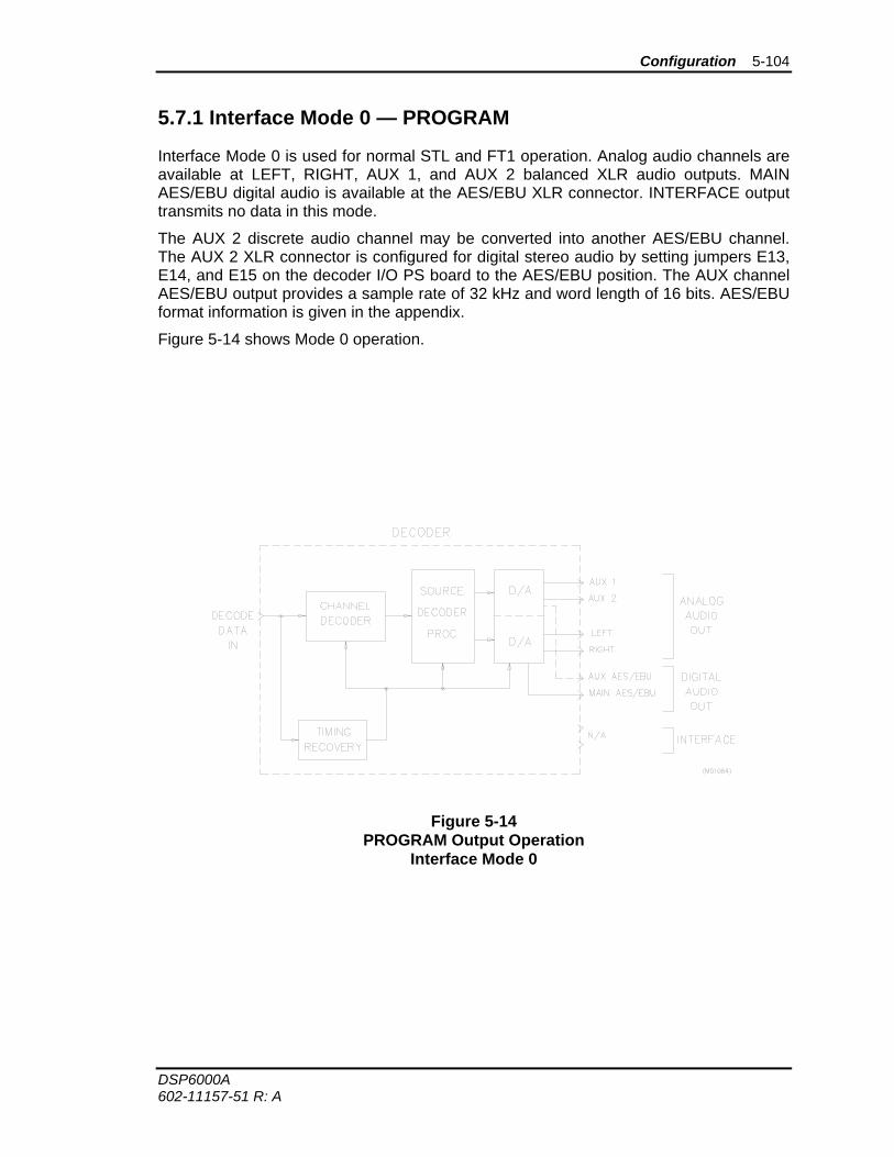
Configuration 5-104
DSP6000A 602-11157-51 R: A
5.7.1 Interface Mode 0 — PROGRAM
Interface Mode 0 is used for normal STL and FT1 operation. Analog audio channels are available at LEFT, RIGHT, AUX 1, and AUX 2 balanced XLR audio outputs. MAIN AES/EBU digital audio is available at the AES/EBU XLR connector. INTERFACE output transmits no data in this mode.
The AUX 2 discrete audio channel may be converted into another AES/EBU channel. The AUX 2 XLR connector is configured for digital stereo audio by setting jumpers E13, E14, and E15 on the decoder I/O PS board to the AES/EBU position. The AUX channel AES/EBU output provides a sample rate of 32 kHz and word length of 16 bits. AES/EBU format information is given in the appendix.
Figure 5-14 shows Mode 0 operation.
Figure 5-14 PROGRAM Output Operation
Interface Mode 0
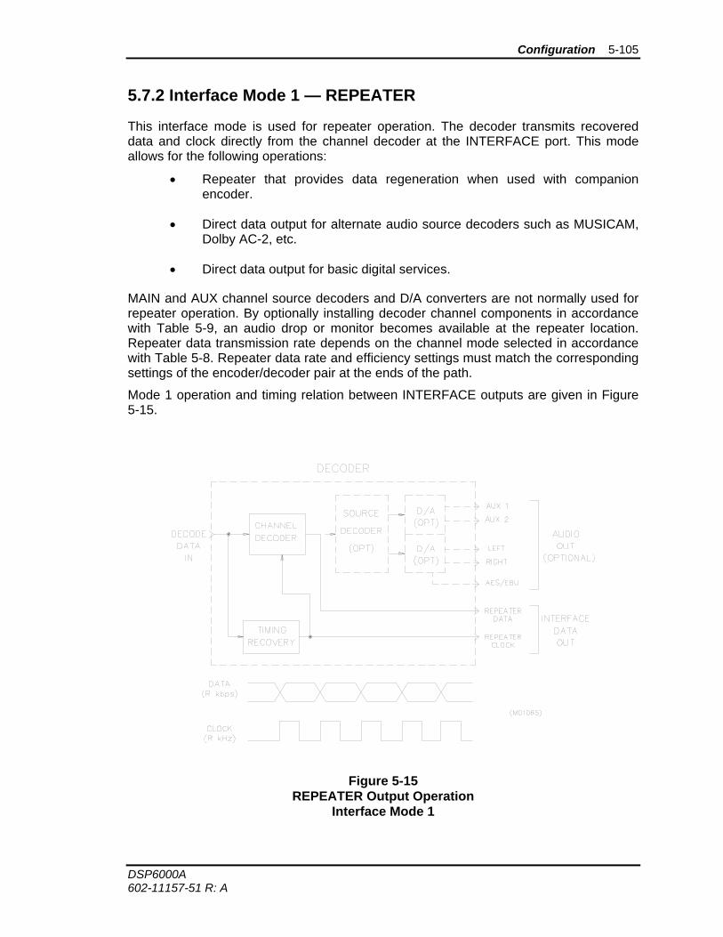
Configuration 5-105
DSP6000A 602-11157-51 R: A
5.7.2 Interface Mode 1 — REPEATER
This interface mode is used for repeater operation. The decoder transmits recovered data and clock directly from the channel decoder at the INTERFACE port. This mode allows for the following operations:
• Repeater that provides data regeneration when used with companion encoder.
• Direct data output for alternate audio source decoders such as MUSICAM, Dolby AC-2, etc.
• Direct data output for basic digital services.
MAIN and AUX channel source decoders and D/A converters are not normally used for repeater operation. By optionally installing decoder channel components in accordance with Table 5-9, an audio drop or monitor becomes available at the repeater location. Repeater data transmission rate depends on the channel mode selected in accordance with Table 5-8. Repeater data rate and efficiency settings must match the corresponding settings of the encoder/decoder pair at the ends of the path.
Mode 1 operation and timing relation between INTERFACE outputs are given in Figure 5-15.
Figure 5-15 REPEATER Output Operation
Interface Mode 1
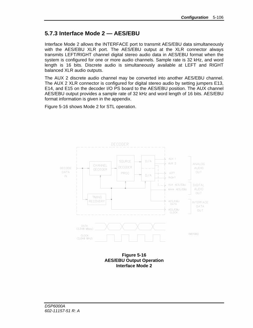
Configuration 5-106
DSP6000A 602-11157-51 R: A
5.7.3 Interface Mode 2 — AES/EBU
Interface Mode 2 allows the INTERFACE port to transmit AES/EBU data simultaneously with the AES/EBU XLR port. The AES/EBU output at the XLR connector always transmits LEFT/RIGHT channel digital stereo audio data in AES/EBU format when the system is configured for one or more audio channels. Sample rate is 32 kHz, and word length is 16 bits. Discrete audio is simultaneously available at LEFT and RIGHT balanced XLR audio outputs.
The AUX 2 discrete audio channel may be converted into another AES/EBU channel. The AUX 2 XLR connector is configured for digital stereo audio by setting jumpers E13, E14, and E15 on the decoder I/O PS board to the AES/EBU position. The AUX channel AES/EBU output provides a sample rate of 32 kHz and word length of 16 bits. AES/EBU format information is given in the appendix.
Figure 5-16 shows Mode 2 for STL operation.
Figure 5-16 AES/EBU Output Operation
Interface Mode 2
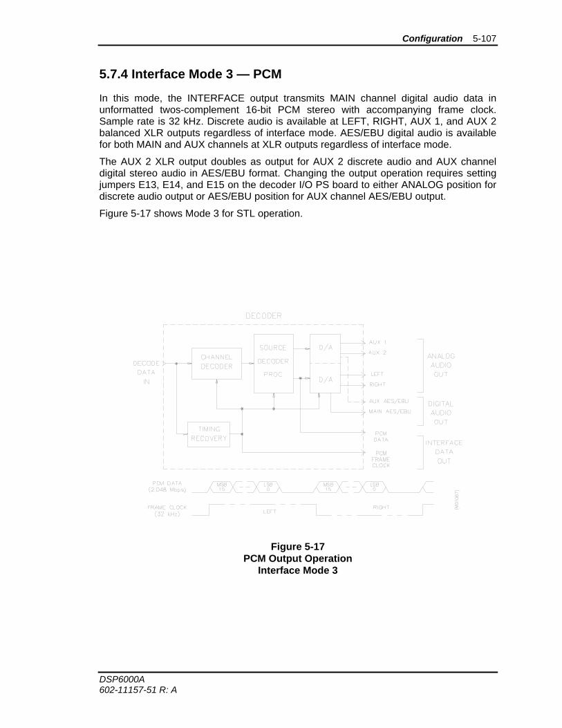
Configuration 5-107
DSP6000A 602-11157-51 R: A
5.7.4 Interface Mode 3 — PCM
In this mode, the INTERFACE output transmits MAIN channel digital audio data in unformatted twos-complement 16-bit PCM stereo with accompanying frame clock. Sample rate is 32 kHz. Discrete audio is available at LEFT, RIGHT, AUX 1, and AUX 2 balanced XLR outputs regardless of interface mode. AES/EBU digital audio is available for both MAIN and AUX channels at XLR outputs regardless of interface mode.
The AUX 2 XLR output doubles as output for AUX 2 discrete audio and AUX channel digital stereo audio in AES/EBU format. Changing the output operation requires setting jumpers E13, E14, and E15 on the decoder I/O PS board to either ANALOG position for discrete audio output or AES/EBU position for AUX channel AES/EBU output.
Figure 5-17 shows Mode 3 for STL operation.
Figure 5-17 PCM Output Operation
Interface Mode 3
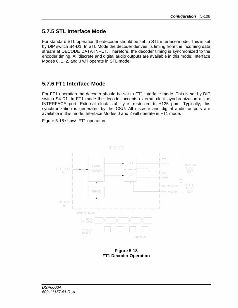
Configuration 5-108
DSP6000A 602-11157-51 R: A
5.7.5 STL Interface Mode
For standard STL operation the decoder should be set to STL interface mode. This is set by DIP switch S4-D1. In STL Mode the decoder derives its timing from the incoming data stream at DECODE DATA INPUT. Therefore, the decoder timing is synchronized to the encoder timing. All discrete and digital audio outputs are available in this mode. Interface Modes 0, 1, 2, and 3 will operate in STL mode.
5.7.6 FT1 Interface Mode
For FT1 operation the decoder should be set to FT1 interface mode. This is set by DIP switch S4-D1. In FT1 mode the decoder accepts external clock synchronization at the INTERFACE port. External clock stability is restricted to ±125 ppm. Typically, this synchronization is generated by the CSU. All discrete and digital audio outputs are available in this mode. Interface Modes 0 and 2 will operate in FT1 mode.
Figure 5-18 shows FT1 operation.
Figure 5-18 FT1 Decoder Operation
Configuration 5-109
DSP6000A 602-11157-51 R: A
5.8 Changing Transmission Efficiency
A spare resistor header, identified as SPARE HDR1 on the circuit board, is stored on the encoder and decoder main processor boards. This header facilitates changes between standard and high efficiency modes when the data rate is not to be changed. The encoder and decoder must be set to the same efficiency. Data rate kits ordered from Moseley Associates include both HDR1 and SPARE HDR1, of the appropriate values for Standard and High efficiencies at the date rate requested.
To change from standard to high efficiency, or vice versa, exchange HDR1 and SPARE HDR1 in both units. Exchanging HDR1 is not required when switching between Standard Efficiency and Standard with Pilot. The decoder’s HDR2 is not exchanged.
Next, make the switch and jumper settings in Table 5-3 (encoder) and Table 5-10 (decoder).
Connect an oscilloscope to ENCODE DATA OUT on the encoder rear panel. Verify the output provides the appropriate waveform and level (see section 5.3).
Set up the test configuration shown in Figure 5-9, and follow the threshold performance procedure given in Sections 5.6.1, 5.6.2, or 5.6.3, depending on the transmission efficiency.
5.9 Data Channel Configuration
The DSP6000A can transmit up to two asynchronous data channels. The ports are wired as Data Communication Equipment (DCE). Data Channel 1 (DATA 1) uses one bit (the LSB) from the MAIN LEFT APTx encoder/decoder pair. This channel can be switched on or off. DATA 2 is multiplexed with the MAIN and AUX audio data within the auxiliary multiplexer, and cannot be disabled. Table 5-16 and Table 5-17 show the DIP switch settings for the two data channels.
Repeater configuration does not allow the use of data channels at the repeater site.
The encoder and decoder must be set identically.
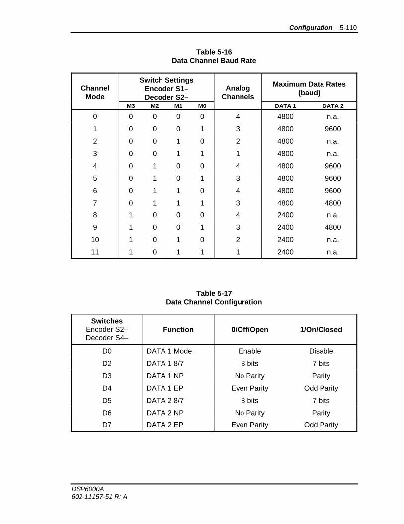
Configuration 5-110
DSP6000A 602-11157-51 R: A
Table 5-16 Data Channel Baud Rate
Channel Mode
Switch Settings Encoder S1– Decoder S2–
Analog Channels
Maximum Data Rates (baud)
M3 M2 M1 M0 DATA 1 DATA 2
0 0 0 0 0 4 4800 n.a.
1 0 0 0 1 3 4800 9600
2 0 0 1 0 2 4800 n.a.
3 0 0 1 1 1 4800 n.a.
4 0 1 0 0 4 4800 9600
5 0 1 0 1 3 4800 9600
6 0 1 1 0 4 4800 9600
7 0 1 1 1 3 4800 4800
8 1 0 0 0 4 2400 n.a.
9 1 0 0 1 3 2400 4800
10 1 0 1 0 2 2400 n.a.
11 1 0 1 1 1 2400 n.a.
Table 5-17 Data Channel Configuration
Switches Encoder S2– Decoder S4–
Function
0/Off/Open
1/On/Closed
D0 DATA 1 Mode Enable Disable
D2 DATA 1 8/7 8 bits 7 bits
D3 DATA 1 NP No Parity Parity
D4 DATA 1 EP Even Parity Odd Parity
D5 DATA 2 8/7 8 bits 7 bits
D6 DATA 2 NP No Parity Parity
D7 DATA 2 EP Even Parity Odd Parity
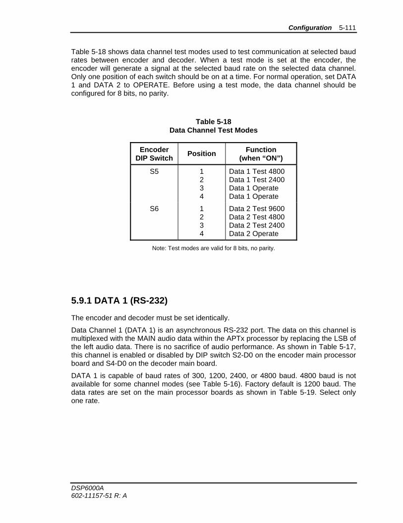
Configuration 5-111
DSP6000A 602-11157-51 R: A
Table 5-18 shows data channel test modes used to test communication at selected baud rates between encoder and decoder. When a test mode is set at the encoder, the encoder will generate a signal at the selected baud rate on the selected data channel. Only one position of each switch should be on at a time. For normal operation, set DATA 1 and DATA 2 to OPERATE. Before using a test mode, the data channel should be configured for 8 bits, no parity.
Table 5-18 Data Channel Test Modes
Encoder DIP Switch Position Function
(when “ON”)
S5 1 2 3 4
Data 1 Test 4800 Data 1 Test 2400 Data 1 Operate Data 1 Operate
S6 1 2 3 4
Data 2 Test 9600 Data 2 Test 4800 Data 2 Test 2400 Data 2 Operate
Note: Test modes are valid for 8 bits, no parity.
5.9.1 DATA 1 (RS-232)
The encoder and decoder must be set identically.
Data Channel 1 (DATA 1) is an asynchronous RS-232 port. The data on this channel is multiplexed with the MAIN audio data within the APTx processor by replacing the LSB of the left audio data. There is no sacrifice of audio performance. As shown in Table 5-17, this channel is enabled or disabled by DIP switch S2-D0 on the encoder main processor board and S4-D0 on the decoder main board.
DATA 1 is capable of baud rates of 300, 1200, 2400, or 4800 baud. 4800 baud is not available for some channel modes (see Table 5-16). Factory default is 1200 baud. The data rates are set on the main processor boards as shown in Table 5-19. Select only one rate.
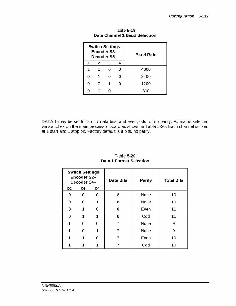
Configuration 5-112
DSP6000A 602-11157-51 R: A
Table 5-19 Data Channel 1 Baud Selection
Switch Settings Encoder S3– Decoder S5– Baud Rate
1 2 3 4
1 0 0 0 4800
0 1 0 0 2400
0 0 1 0 1200
0 0 0 1 300
DATA 1 may be set for 8 or 7 data bits, and even, odd, or no parity. Format is selected via switches on the main processor board as shown in Table 5-20. Each channel is fixed at 1 start and 1 stop bit. Factory default is 8 bits, no parity.
Table 5-20 Data 1 Format Selection
Switch Settings Encoder S2– Decoder S4– Data Bits Parity Total Bits
D2 D3 D4
0 0 0 8 None 10
0 0 1 8 None 10
0 1 0 8 Even 11
0 1 1 8 Odd 11
1 0 0 7 None 9
1 0 1 7 None 9
1 1 0 7 Even 10
1 1 1 7 Odd 10
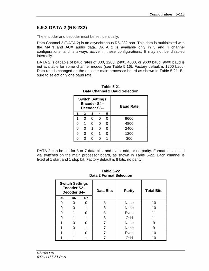
Configuration 5-113
DSP6000A 602-11157-51 R: A
5.9.2 DATA 2 (RS-232)
The encoder and decoder must be set identically.
Data Channel 2 (DATA 2) is an asynchronous RS-232 port. This data is multiplexed with the MAIN and AUX audio data. DATA 2 is available only in 3 and 4 channel configurations, and is always active in these configurations. It may not be disabled internally.
DATA 2 is capable of baud rates of 300, 1200, 2400, 4800, or 9600 baud. 9600 baud is not available for some channel modes (see Table 5-16). Factory default is 1200 baud. Data rate is changed on the encoder main processor board as shown in Table 5-21. Be sure to select only one baud rate.
Table 5-21 Data Channel 2 Baud Selection
Switch Settings Encoder S4– Decoder S6– Baud Rate
1 2 3 4 5 1 0 0 0 0 9600 0 1 0 0 0 4800 0 0 1 0 0 2400 0 0 0 1 0 1200 0 0 0 0 1 300
DATA 2 can be set for 8 or 7 data bits, and even, odd, or no parity. Format is selected via switches on the main processor board, as shown in Table 5-22. Each channel is fixed at 1 start and 1 stop bit. Factory default is 8 bits, no parity.
Table 5-22 Data 2 Format Selection
Switch Settings Encoder S2– Decoder S4– Data Bits Parity Total Bits
D5 D6 D7 0 0 0 8 None 10 0 0 1 8 None 10 0 1 0 8 Even 11 0 1 1 8 Odd 11 1 0 0 7 None 9 1 0 1 7 None 9 1 1 0 7 Even 10 1 1 1 7 Odd 10
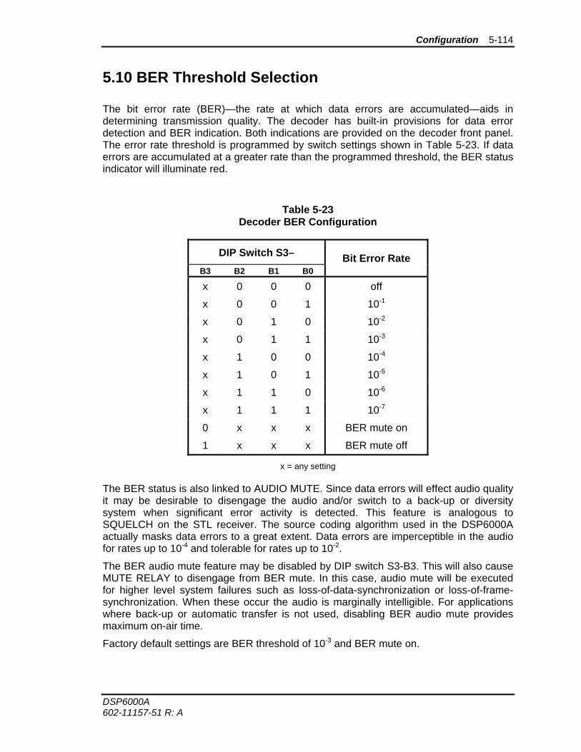
Configuration 5-114
DSP6000A 602-11157-51 R: A
5.10 BER Threshold Selection
The bit error rate (BER)—the rate at which data errors are accumulated—aids in determining transmission quality. The decoder has built-in provisions for data error detection and BER indication. Both indications are provided on the decoder front panel. The error rate threshold is programmed by switch settings shown in Table 5-23. If data errors are accumulated at a greater rate than the programmed threshold, the BER status indicator will illuminate red.
Table 5-23 Decoder BER Configuration
DIP Switch S3– Bit Error Rate B3 B2 B1 B0
x 0 0 0 off
x 0 0 1 10-1
x 0 1 0 10-2
x 0 1 1 10-3
x 1 0 0 10-4
x 1 0 1 10-5
x 1 1 0 10-6
x 1 1 1 10-7
0 x x x BER mute on
1 x x x BER mute off
x = any setting
The BER status is also linked to AUDIO MUTE. Since data errors will effect audio quality it may be desirable to disengage the audio and/or switch to a back-up or diversity system when significant error activity is detected. This feature is analogous to SQUELCH on the STL receiver. The source coding algorithm used in the DSP6000A actually masks data errors to a great extent. Data errors are imperceptible in the audio for rates up to 10-4 and tolerable for rates up to 10-2.
The BER audio mute feature may be disabled by DIP switch S3-B3. This will also cause MUTE RELAY to disengage from BER mute. In this case, audio mute will be executed for higher level system failures such as loss-of-data-synchronization or loss-of-frame-synchronization. When these occur the audio is marginally intelligible. For applications where back-up or automatic transfer is not used, disabling BER audio mute provides maximum on-air time.
Factory default settings are BER threshold of 10-3 and BER mute on.
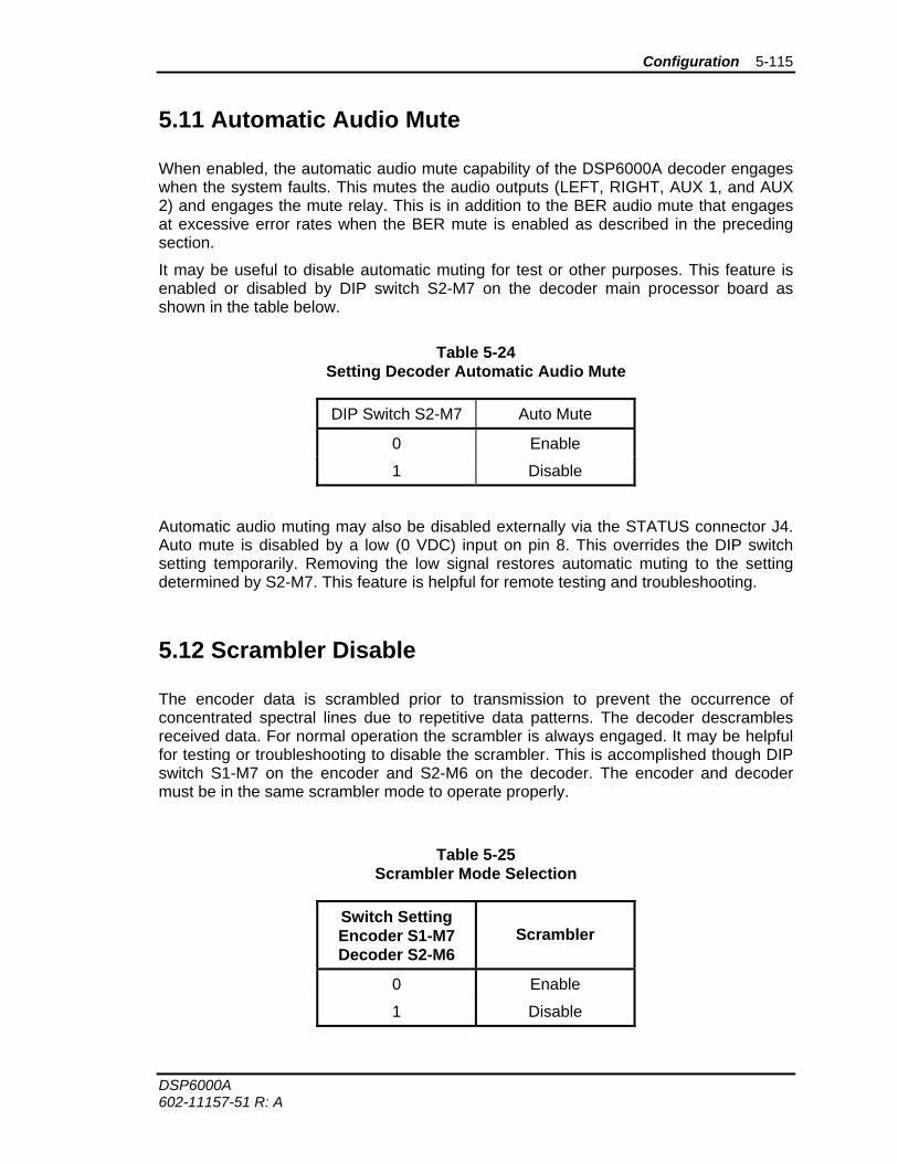
Configuration 5-115
DSP6000A 602-11157-51 R: A
5.11 Automatic Audio Mute
When enabled, the automatic audio mute capability of the DSP6000A decoder engages when the system faults. This mutes the audio outputs (LEFT, RIGHT, AUX 1, and AUX 2) and engages the mute relay. This is in addition to the BER audio mute that engages at excessive error rates when the BER mute is enabled as described in the preceding section.
It may be useful to disable automatic muting for test or other purposes. This feature is enabled or disabled by DIP switch S2-M7 on the decoder main processor board as shown in the table below.
Table 5-24 Setting Decoder Automatic Audio Mute
DIP Switch S2-M7 Auto Mute
0 Enable
1 Disable
Automatic audio muting may also be disabled externally via the STATUS connector J4. Auto mute is disabled by a low (0 VDC) input on pin 8. This overrides the DIP switch setting temporarily. Removing the low signal restores automatic muting to the setting determined by S2-M7. This feature is helpful for remote testing and troubleshooting.
5.12 Scrambler Disable
The encoder data is scrambled prior to transmission to prevent the occurrence of concentrated spectral lines due to repetitive data patterns. The decoder descrambles received data. For normal operation the scrambler is always engaged. It may be helpful for testing or troubleshooting to disable the scrambler. This is accomplished though DIP switch S1-M7 on the encoder and S2-M6 on the decoder. The encoder and decoder must be in the same scrambler mode to operate properly.
Table 5-25 Scrambler Mode Selection
Switch Setting Encoder S1-M7 Decoder S2-M6
Scrambler
0 Enable
1 Disable
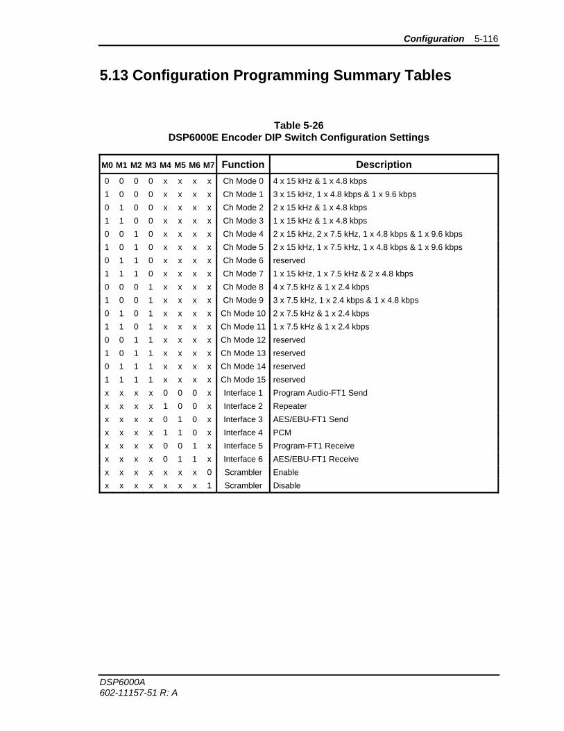
Configuration 5-116
DSP6000A 602-11157-51 R: A
5.13 Configuration Programming Summary Tables
Table 5-26
DSP6000E Encoder DIP Switch Configuration Settings
M0 M1 M2 M3 M4 M5 M6 M7 Function Description 0 0 0 0 x x x x Ch Mode 0 4 x 15 kHz & 1 x 4.8 kbps 1 0 0 0 x x x x Ch Mode 1 3 x 15 kHz, 1 x 4.8 kbps & 1 x 9.6 kbps 0 1 0 0 x x x x Ch Mode 2 2 x 15 kHz & 1 x 4.8 kbps 1 1 0 0 x x x x Ch Mode 3 1 x 15 kHz & 1 x 4.8 kbps 0 0 1 0 x x x x Ch Mode 4 2 x 15 kHz, 2 x 7.5 kHz, 1 x 4.8 kbps & 1 x 9.6 kbps 1 0 1 0 x x x x Ch Mode 5 2 x 15 kHz, 1 x 7.5 kHz, 1 x 4.8 kbps & 1 x 9.6 kbps 0 1 1 0 x x x x Ch Mode 6 reserved 1 1 1 0 x x x x Ch Mode 7 1 x 15 kHz, 1 x 7.5 kHz & 2 x 4.8 kbps 0 0 0 1 x x x x Ch Mode 8 4 x 7.5 kHz & 1 x 2.4 kbps 1 0 0 1 x x x x Ch Mode 9 3 x 7.5 kHz, 1 x 2.4 kbps & 1 x 4.8 kbps 0 1 0 1 x x x x Ch Mode 10 2 x 7.5 kHz & 1 x 2.4 kbps 1 1 0 1 x x x x Ch Mode 11 1 x 7.5 kHz & 1 x 2.4 kbps 0 0 1 1 x x x x Ch Mode 12 reserved 1 0 1 1 x x x x Ch Mode 13 reserved 0 1 1 1 x x x x Ch Mode 14 reserved 1 1 1 1 x x x x Ch Mode 15 reserved x x x x 0 0 0 x Interface 1 Program Audio-FT1 Send x x x x 1 0 0 x Interface 2 Repeater x x x x 0 1 0 x Interface 3 AES/EBU-FT1 Send x x x x 1 1 0 x Interface 4 PCM x x x x 0 0 1 x Interface 5 Program-FT1 Receive x x x x 0 1 1 x Interface 6 AES/EBU-FT1 Receive x x x x x x x 0 Scrambler Enable x x x x x x x 1 Scrambler Disable
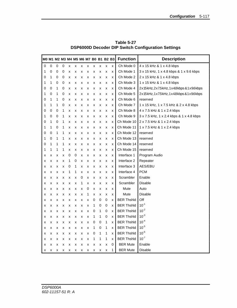
Configuration 5-117
DSP6000A 602-11157-51 R: A
Table 5-27 DSP6000D Decoder DIP Switch Configuration Settings
M0 M1 M2 M3 M4 M5 M6 M7 B0 B1 B2 B3 Function Description 0 0 0 0 x x x x x x x x Ch Mode 0 4 x 15 kHz & 1 x 4.8 kbps 1 0 0 0 x x x x x x x x Ch Mode 1 3 x 15 kHz, 1 x 4.8 kbps & 1 x 9.6 kbps 0 1 0 0 x x x x x x x x Ch Mode 2 2 x 15 kHz & 1 x 4.8 kbps 1 1 0 0 x x x x x x x x Ch Mode 3 1 x 15 kHz & 1 x 4.8 kbps 0 0 1 0 x x x x x x x x Ch Mode 4 2 x 15 kHz, 2 x 7.5 kHz, 1 x 4.8 kbps & 1 x 9.6 kbps 1 0 1 0 x x x x x x x x Ch Mode 5 2 x 15 kHz, 1 x 7.5 kHz, 1 x 4.8 kbps & 1 x 9.6 kbps 0 1 1 0 x x x x x x x x Ch Mode 6 reserved 1 1 1 0 x x x x x x x x Ch Mode 7 1 x 15 kHz, 1 x 7.5 kHz & 2 x 4.8 kbps 0 0 0 1 x x x x x x x x Ch Mode 8 4 x 7.5 kHz & 1 x 2.4 kbps 1 0 0 1 x x x x x x x x Ch Mode 9 3 x 7.5 kHz, 1 x 2.4 kbps & 1 x 4.8 kbps 0 1 0 1 x x x x x x x x Ch Mode 10 2 x 7.5 kHz & 1 x 2.4 kbps 1 1 0 1 x x x x x x x x Ch Mode 11 1 x 7.5 kHz & 1 x 2.4 kbps 0 0 1 1 x x x x x x x x Ch Mode 12 reserved 1 0 1 1 x x x x x x x x Ch Mode 13 reserved 0 1 1 1 x x x x x x x x Ch Mode 14 reserved 1 1 1 1 x x x x x x x x Ch Mode 15 reserved x x x x 0 0 x x x x x x Interface 1 Program Audio x x x x 1 0 x x x x x x Interface 2 Repeater x x x x 0 1 x x x x x x Interface 3 AES/EBU x x x x 1 1 x x x x x x Interface 4 PCM x x x x x x 0 x x x x x Scrambler Enable x x x x x x 1 x x x x x Scrambler Disable x x x x x x x 0 x x x x Mute Auto x x x x x x x 1 x x x x Mute Disable x x x x x x x x 0 0 0 x BER Thshld Off x x x x x x x x 1 0 0 x BER Thshld 10-1 x x x x x x x x 0 1 0 x BER Thshld 10-2 x x x x x x x x 1 1 0 x BER Thshld 10-3 x x x x x x x x 0 0 1 x BER Thshld 10-4 x x x x x x x x 1 0 1 x BER Thshld 10-5 x x x x x x x x 0 1 1 x BER Thshld 10-6 x x x x x x x x 1 1 1 x BER Thshld 10-7 x x x x x x x x x x x 0 BER Mute Enable x x x x x x x x x x x 1 BER Mute Disable
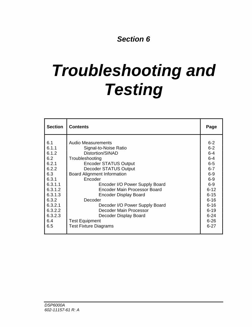
DSP6000A 602-11157-61 R: A
Section 6
Troubleshooting and Testing
Section Contents Page
6.1 Audio Measurements 6-2 6.1.1 Signal-to-Noise Ratio 6-2 6.1.2 Distortion/SINAD 6-4 6.2 Troubleshooting 6-4 6.2.1 Encoder STATUS Output 6-5 6.2.2 Decoder STATUS Output 6-7 6.3 Board Alignment Information 6-9 6.3.1 Encoder 6-9 6.3.1.1 Encoder I/O Power Supply Board 6-9 6.3.1.2 Encoder Main Processor Board 6-12 6.3.1.3 Encoder Display Board 6-15 6.3.2 Decoder 6-16 6.3.2.1 Decoder I/O Power Supply Board 6-16 6.3.2.2 Decoder Main Processor 6-19 6.3.2.3 Decoder Display Board 6-24 6.4 Test Equipment 6-26 6.5 Test Fixture Diagrams 6-27
Troubleshooting and Testing 6-119
DSP6000A 602-11157-61 R: A
6.1 Audio Measurements
This section is intended to help the user better understand what to expect from audio measurements of the DSP6000A system. The DSP6000A is based on techniques of digital audio processing technology that provide high quality audio reproduction, but these techniques add special requirements during audio testing. Familiarity with the following technologies will prevent suprises during testing.
The DSP6000A uses digital audio data reduction techniques that render traditional harmonic distortion measurements meaningless. The data reduction algorithm (aptX-100, 4:1 reduction) makes it possible to transmit “spectrum hungry” digital audio over narrow radio channels or telco lines. This algorithm removes redundant audio information by means of subband coding and places the resulting quantizing noise into audio regions within the passband that are not acoustically relevant to the hearing process. Perceptually, the audio is perfect. Standard wideband distortion or SINAD measurements, however, will measure this quantizing noise that the ear does not hear. We recommend measuring harmonic distortion using a spectrum analyzer and calculating the total harmonic content as described below.
The delta-sigma D/A conversion process used in the DSP6000A, on the other hand, places the quantizing noise well outside the audio passband. By means of digital noise-shaping the output noise floor slowly rises to a peak at about 60 kHz (32 kHz sample rate). A wideband signal-to-noise measurement sees this out-of-band noise peak as excessive noise or poor SNR. Therefore, place a 22 kHz low-pass filter preceding the test set for signal-to-noise measurements. In essence, take care not to measure what the ear cannot hear.
6.1.1 Signal-to-Noise Ratio
The signal-to-noise ratio measurement will provide the user with the usable dynamic range of the DSP6000A system. This is a static measurement.
Test Equipment
Distortion Analyzer and Signal Source, Audio Precision System 1 or equivalent.
Procedure
1. Set up the equipment as indicated in Figure 6-1.
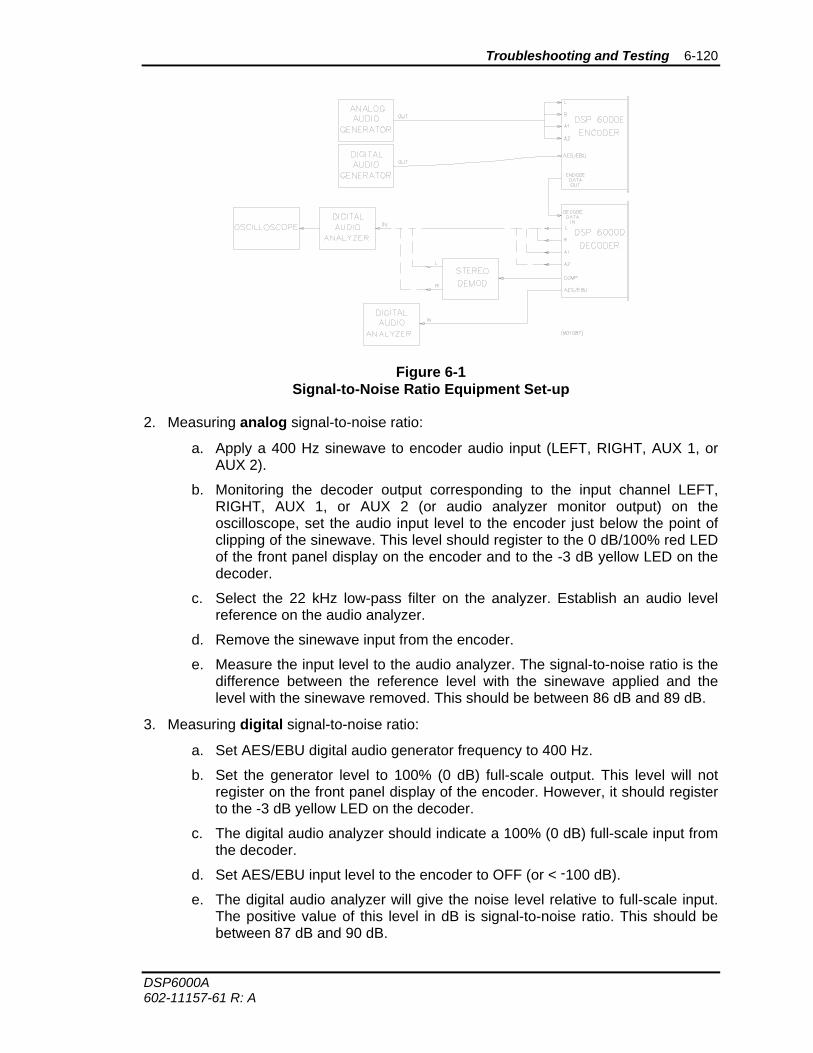
Troubleshooting and Testing 6-120
DSP6000A 602-11157-61 R: A
Figure 6-1 Signal-to-Noise Ratio Equipment Set-up
2. Measuring analog signal-to-noise ratio:
a. Apply a 400 Hz sinewave to encoder audio input (LEFT, RIGHT, AUX 1, or AUX 2).
b. Monitoring the decoder output corresponding to the input channel LEFT, RIGHT, AUX 1, or AUX 2 (or audio analyzer monitor output) on the oscilloscope, set the audio input level to the encoder just below the point of clipping of the sinewave. This level should register to the 0 dB/100% red LED of the front panel display on the encoder and to the -3 dB yellow LED on the decoder.
c. Select the 22 kHz low-pass filter on the analyzer. Establish an audio level reference on the audio analyzer.
d. Remove the sinewave input from the encoder.
e. Measure the input level to the audio analyzer. The signal-to-noise ratio is the difference between the reference level with the sinewave applied and the level with the sinewave removed. This should be between 86 dB and 89 dB.
3. Measuring digital signal-to-noise ratio:
a. Set AES/EBU digital audio generator frequency to 400 Hz.
b. Set the generator level to 100% (0 dB) full-scale output. This level will not register on the front panel display of the encoder. However, it should register to the -3 dB yellow LED on the decoder.
c. The digital audio analyzer should indicate a 100% (0 dB) full-scale input from the decoder.
d. Set AES/EBU input level to the encoder to OFF (or < -100 dB).
e. The digital audio analyzer will give the noise level relative to full-scale input. The positive value of this level in dB is signal-to-noise ratio. This should be between 87 dB and 90 dB.
Troubleshooting and Testing 6-121
DSP6000A 602-11157-61 R: A
6.1.2 Distortion/SINAD
Traditional dynamic measurements such as wideband distortion or SINAD will produce erroneous results. These measurement techniques will measure audio artifacts that are irrelevant to the hearing process. Harmonic distortion may be measured, though, since harmonic distortion is not part of the masking process. A traditional total harmonic distortion (THD) may be accomplished by measuring the amplitude of each harmonic on a spectrum analyzer. THD is equal to the square root of the sum of the squares of the relative harmonic levels.
6.2 Troubleshooting
This section is intended to aid in troubleshooting the DSP6000A system in the event of a system failure.
In general, first check the DIP switches for proper configuration. Check inputs and outputs for proper connections. Check the power supplies for +5V, +15V, and -15V. Then check the alignment of the system.
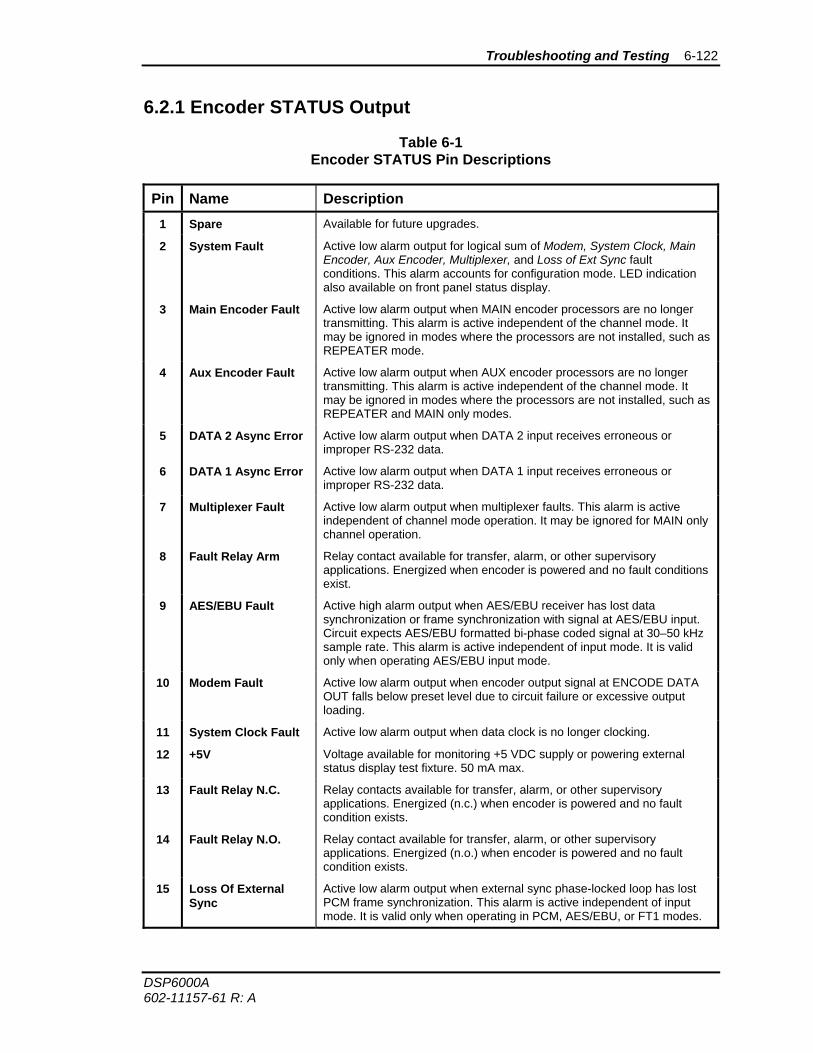
Troubleshooting and Testing 6-122
DSP6000A 602-11157-61 R: A
6.2.1 Encoder STATUS Output
Table 6-1 Encoder STATUS Pin Descriptions
Pin Name Description 1 Spare Available for future upgrades.
2 System Fault Active low alarm output for logical sum of Modem, System Clock, Main Encoder, Aux Encoder, Multiplexer, and Loss of Ext Sync fault conditions. This alarm accounts for configuration mode. LED indication also available on front panel status display.
3 Main Encoder Fault Active low alarm output when MAIN encoder processors are no longer transmitting. This alarm is active independent of the channel mode. It may be ignored in modes where the processors are not installed, such as REPEATER mode.
4 Aux Encoder Fault Active low alarm output when AUX encoder processors are no longer transmitting. This alarm is active independent of the channel mode. It may be ignored in modes where the processors are not installed, such as REPEATER and MAIN only modes.
5 DATA 2 Async Error Active low alarm output when DATA 2 input receives erroneous or improper RS-232 data.
6 DATA 1 Async Error Active low alarm output when DATA 1 input receives erroneous or improper RS-232 data.
7 Multiplexer Fault Active low alarm output when multiplexer faults. This alarm is active independent of channel mode operation. It may be ignored for MAIN only channel operation.
8 Fault Relay Arm Relay contact available for transfer, alarm, or other supervisory applications. Energized when encoder is powered and no fault conditions exist.
9 AES/EBU Fault Active high alarm output when AES/EBU receiver has lost data synchronization or frame synchronization with signal at AES/EBU input. Circuit expects AES/EBU formatted bi-phase coded signal at 30–50 kHz sample rate. This alarm is active independent of input mode. It is valid only when operating AES/EBU input mode.
10 Modem Fault Active low alarm output when encoder output signal at ENCODE DATA OUT falls below preset level due to circuit failure or excessive output loading.
11 System Clock Fault Active low alarm output when data clock is no longer clocking.
12 +5V Voltage available for monitoring +5 VDC supply or powering external status display test fixture. 50 mA max.
13 Fault Relay N.C. Relay contacts available for transfer, alarm, or other supervisory applications. Energized (n.c.) when encoder is powered and no fault condition exists.
14 Fault Relay N.O. Relay contact available for transfer, alarm, or other supervisory applications. Energized (n.o.) when encoder is powered and no fault condition exists.
15 Loss Of External Sync
Active low alarm output when external sync phase-locked loop has lost PCM frame synchronization. This alarm is active independent of input mode. It is valid only when operating in PCM, AES/EBU, or FT1 modes.
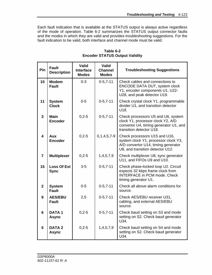
Troubleshooting and Testing 6-123
DSP6000A 602-11157-61 R: A
Each fault indication that is available at the STATUS output is always active regardless of the mode of operation. Table 6-2 summarizes the STATUS output connector faults and the modes in which they are valid and provides troubleshooting suggestions. For the fault indication to be valid, both interface and channel mode must be valid.
Table 6-2 Encoder STATUS Output Validity
Pin Fault Description
Valid Interface Modes
Valid Channel Modes
Troubleshooting Suggestions
10 Modem Fault
0-3 0-5,7-11 Check cables and connections to ENCODE DATA OUT, system clock Y1, encoder components U1, U22-U28, and peak detector U19.
11 System Clock
0-5 0-5,7-11 Check crystal clock Y1, programmable divider U1, and transition detector U18.
3 Main Encoder
0,2-5 0-5,7-11 Check processors U5 and U6, system clock Y1, processor clock Y2, A/D convertor U4, timing generator U1, and transition detector U18.
4 Aux Encoder
0,2-5 0,1,4,5,7-9 Check processors U15 and U16, system clock Y1, processor clock Y3, A/D convertor U14, timing generator U8, and transition detector U12.
7 Multiplexer 0,2-5 1,4,5,7,9 Check multiplexer U8, sync generator U11, and FIFOs U9 and U10.
15 Loss Of Ext Sync
3-5 0-5,7-11 Check phase-locked loop U2. Circuit expects 32 kbps frame clock from INTERFACE in PCM mode. Check timing generator U1.
2 System Fault
0-5 0-5,7-11 Check all above alarm conditions for source.
9 AES/EBU Fault
2,5 0-5,7-11 Check AES/EBU receiver U31, cabling, and external AES/EBU source.
6 DATA 1 Async
0,2-5 0-5,7-11 Check baud setting on S3 and mode setting on S2. Check baud generator U34.
5 DATA 2 Async
0,2-5 1,4,5,7,9 Check baud setting on S4 and mode setting on S2. Check baud generator U34.
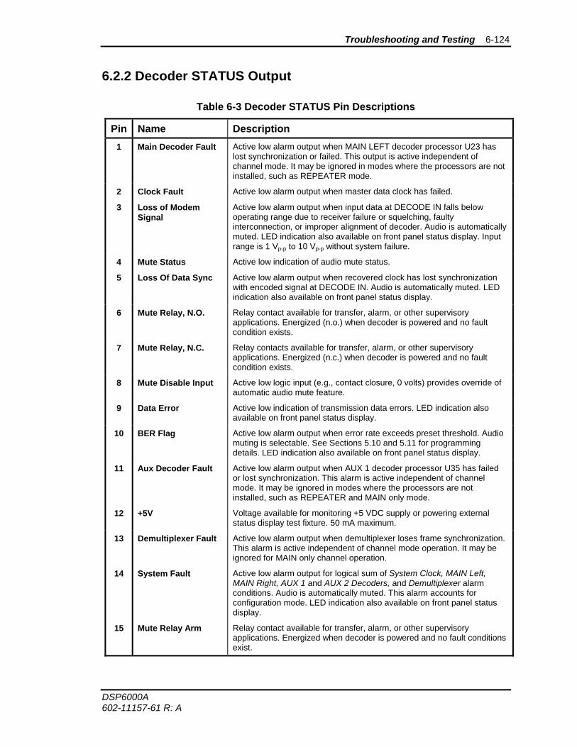
Troubleshooting and Testing 6-124
DSP6000A 602-11157-61 R: A
6.2.2 Decoder STATUS Output
Table 6-3 Decoder STATUS Pin Descriptions
Pin Name Description 1 Main Decoder Fault Active low alarm output when MAIN LEFT decoder processor U23 has
lost synchronization or failed. This output is active independent of channel mode. It may be ignored in modes where the processors are not installed, such as REPEATER mode.
2 Clock Fault Active low alarm output when master data clock has failed.
3 Loss of Modem Signal
Active low alarm output when input data at DECODE IN falls below operating range due to receiver failure or squelching, faulty interconnection, or improper alignment of decoder. Audio is automatically muted. LED indication also available on front panel status display. Input range is 1 Vp-p to 10 Vp-p without system failure.
4 Mute Status Active low indication of audio mute status.
5 Loss Of Data Sync Active low alarm output when recovered clock has lost synchronization with encoded signal at DECODE IN. Audio is automatically muted. LED indication also available on front panel status display.
6 Mute Relay, N.O. Relay contact available for transfer, alarm, or other supervisory applications. Energized (n.o.) when decoder is powered and no fault condition exists.
7 Mute Relay, N.C. Relay contacts available for transfer, alarm, or other supervisory applications. Energized (n.c.) when decoder is powered and no fault condition exists.
8 Mute Disable Input Active low logic input (e.g., contact closure, 0 volts) provides override of automatic audio mute feature.
9 Data Error Active low indication of transmission data errors. LED indication also available on front panel status display.
10 BER Flag Active low alarm output when error rate exceeds preset threshold. Audio muting is selectable. See Sections 5.10 and 5.11 for programming details. LED indication also available on front panel status display.
11 Aux Decoder Fault Active low alarm output when AUX 1 decoder processor U35 has failed or lost synchronization. This alarm is active independent of channel mode. It may be ignored in modes where the processors are not installed, such as REPEATER and MAIN only mode.
12 +5V Voltage available for monitoring +5 VDC supply or powering external status display test fixture. 50 mA maximum.
13 Demultiplexer Fault Active low alarm output when demultiplexer loses frame synchronization. This alarm is active independent of channel mode operation. It may be ignored for MAIN only channel operation.
14 System Fault Active low alarm output for logical sum of System Clock, MAIN Left, MAIN Right, AUX 1 and AUX 2 Decoders, and Demultiplexer alarm conditions. Audio is automatically muted. This alarm accounts for configuration mode. LED indication also available on front panel status display.
15 Mute Relay Arm Relay contact available for transfer, alarm, or other supervisory applications. Energized when decoder is powered and no fault conditions exist.
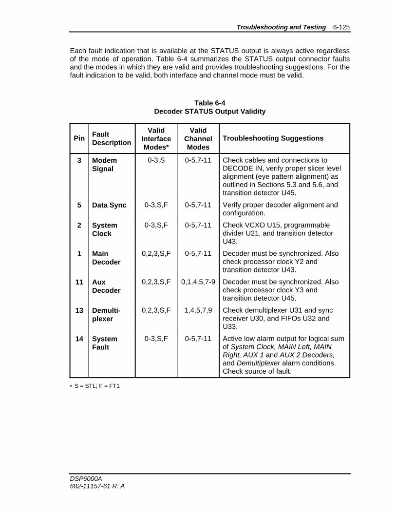
Troubleshooting and Testing 6-125
DSP6000A 602-11157-61 R: A
Each fault indication that is available at the STATUS output is always active regardless of the mode of operation. Table 6-4 summarizes the STATUS output connector faults and the modes in which they are valid and provides troubleshooting suggestions. For the fault indication to be valid, both interface and channel mode must be valid.
Table 6-4 Decoder STATUS Output Validity
Pin Fault Description
Valid Interface Modes*
Valid Channel Modes
Troubleshooting Suggestions
3 Modem Signal
0-3,S 0-5,7-11 Check cables and connections to DECODE IN, verify proper slicer level alignment (eye pattern alignment) as outlined in Sections 5.3 and 5.6, and transition detector U45.
5 Data Sync 0-3,S,F 0-5,7-11 Verify proper decoder alignment and configuration.
2 System Clock
0-3,S,F 0-5,7-11 Check VCXO U15, programmable divider U21, and transition detector U43.
1 Main Decoder
0,2,3,S,F 0-5,7-11 Decoder must be synchronized. Also check processor clock Y2 and transition detector U43.
11 Aux Decoder
0,2,3,S,F 0,1,4,5,7-9 Decoder must be synchronized. Also check processor clock Y3 and transition detector U45.
13 Demulti-plexer
0,2,3,S,F 1,4,5,7,9 Check demultiplexer U31 and sync receiver U30, and FIFOs U32 and U33.
14 System Fault
0-3,S,F 0-5,7-11 Active low alarm output for logical sum of System Clock, MAIN Left, MAIN Right, AUX 1 and AUX 2 Decoders, and Demultiplexer alarm conditions. Check source of fault.
∗ S = STL; F = FT1
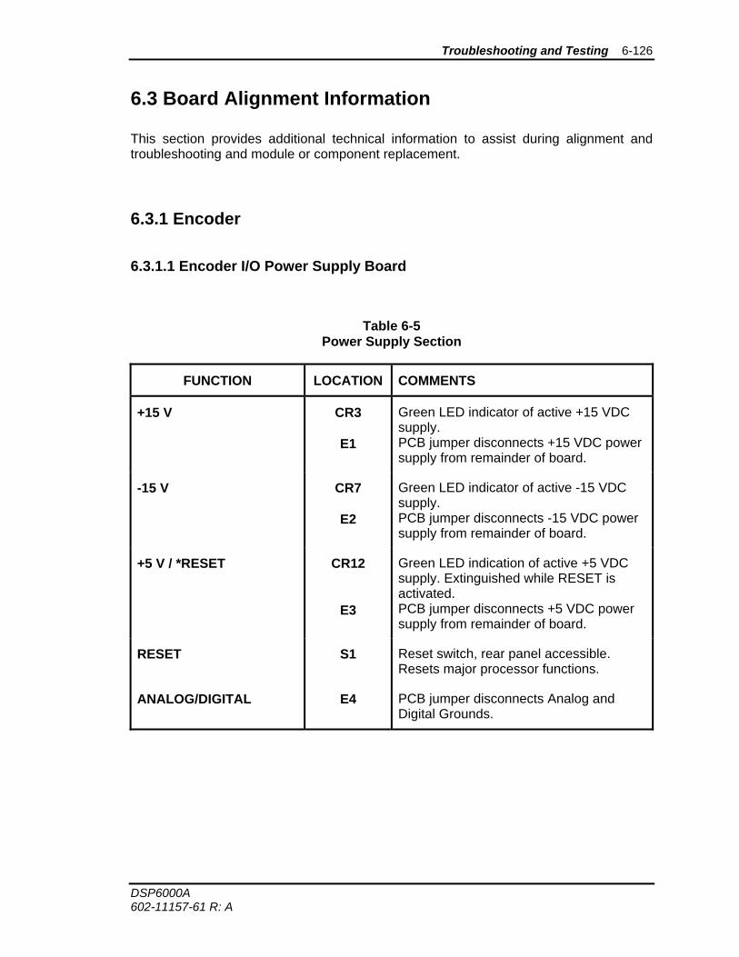
Troubleshooting and Testing 6-126
DSP6000A 602-11157-61 R: A
6.3 Board Alignment Information
This section provides additional technical information to assist during alignment and troubleshooting and module or component replacement.
6.3.1 Encoder
6.3.1.1 Encoder I/O Power Supply Board
Table 6-5 Power Supply Section
FUNCTION LOCATION COMMENTS
+15 V CR3
E1
Green LED indicator of active +15 VDC supply. PCB jumper disconnects +15 VDC power supply from remainder of board.
-15 V CR7
E2
Green LED indicator of active -15 VDC supply. PCB jumper disconnects -15 VDC power supply from remainder of board.
+5 V / *RESET CR12
E3
Green LED indication of active +5 VDC supply. Extinguished while RESET is activated. PCB jumper disconnects +5 VDC power supply from remainder of board.
RESET S1 Reset switch, rear panel accessible. Resets major processor functions.
ANALOG/DIGITAL E4 PCB jumper disconnects Analog and Digital Grounds.
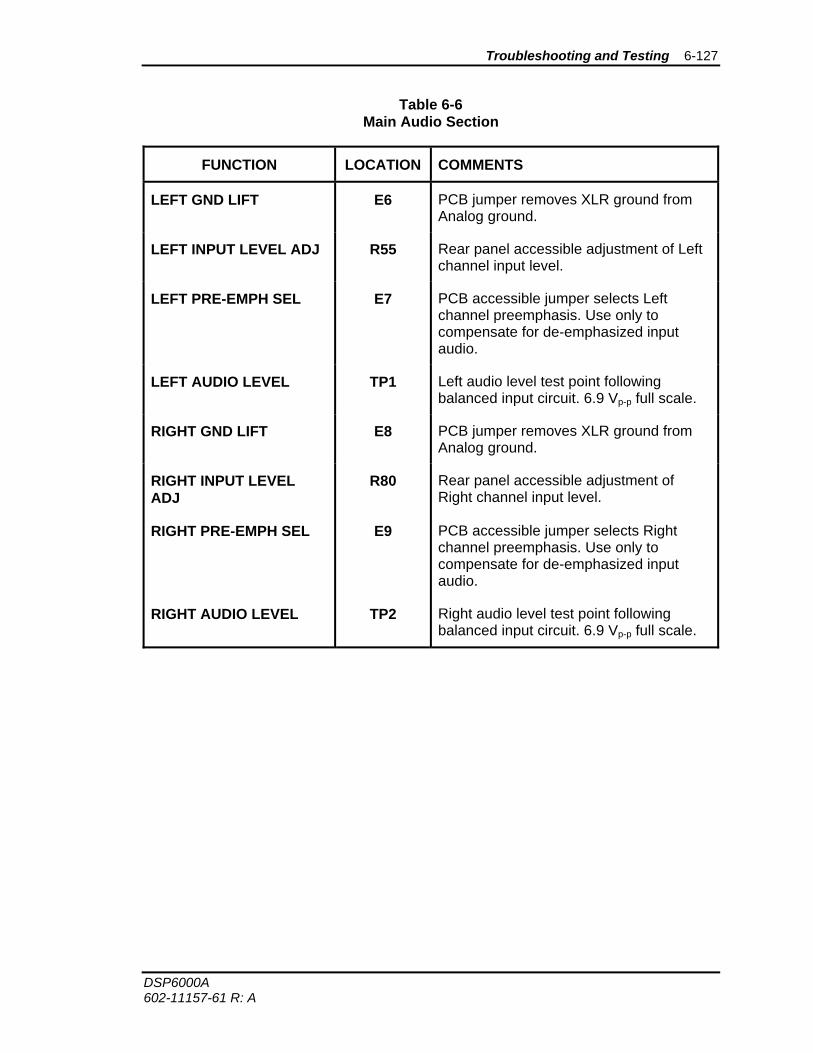
Troubleshooting and Testing 6-127
DSP6000A 602-11157-61 R: A
Table 6-6 Main Audio Section
FUNCTION LOCATION COMMENTS
LEFT GND LIFT E6 PCB jumper removes XLR ground from Analog ground.
LEFT INPUT LEVEL ADJ R55 Rear panel accessible adjustment of Left channel input level.
LEFT PRE-EMPH SEL E7 PCB accessible jumper selects Left channel preemphasis. Use only to compensate for de-emphasized input audio.
LEFT AUDIO LEVEL TP1 Left audio level test point following balanced input circuit. 6.9 Vp-p full scale.
RIGHT GND LIFT E8 PCB jumper removes XLR ground from Analog ground.
RIGHT INPUT LEVEL ADJ
R80 Rear panel accessible adjustment of Right channel input level.
RIGHT PRE-EMPH SEL E9 PCB accessible jumper selects Right channel preemphasis. Use only to compensate for de-emphasized input audio.
RIGHT AUDIO LEVEL TP2 Right audio level test point following balanced input circuit. 6.9 Vp-p full scale.
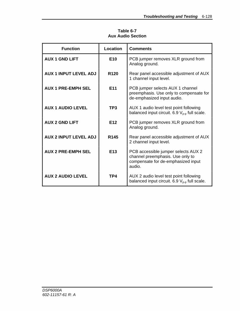
Troubleshooting and Testing 6-128
DSP6000A 602-11157-61 R: A
Table 6-7 Aux Audio Section
Function Location Comments
AUX 1 GND LIFT E10 PCB jumper removes XLR ground from Analog ground.
AUX 1 INPUT LEVEL ADJ R120 Rear panel accessible adjustment of AUX 1 channel input level.
AUX 1 PRE-EMPH SEL E11 PCB jumper selects AUX 1 channel preemphasis. Use only to compensate for de-emphasized input audio.
AUX 1 AUDIO LEVEL TP3 AUX 1 audio level test point following balanced input circuit. 6.9 Vp-p full scale.
AUX 2 GND LIFT E12 PCB jumper removes XLR ground from Analog ground.
AUX 2 INPUT LEVEL ADJ R145 Rear panel accessible adjustment of AUX 2 channel input level.
AUX 2 PRE-EMPH SEL E13 PCB accessible jumper selects AUX 2 channel preemphasis. Use only to compensate for de-emphasized input audio.
AUX 2 AUDIO LEVEL TP4 AUX 2 audio level test point following balanced input circuit. 6.9 Vp-p full scale.

Troubleshooting and Testing 6-129
DSP6000A 602-11157-61 R: A
6.3.1.2 Encoder Main Processor Board
Table 6-8 External Sync Section
Function Location Comments
EXT SYNC AFC ADJ R3 PCB accessible adjustment of External Sync (clock) phase-locked loop.
EXT SYNC AFC LEVEL TP2 External Sync AFC Level, 1.1–3.9 VDC. Should be set for 2.5 VDC nominal when external clock input is present.
EXT SYNC LED CR1 Red LED is illuminated when External Sync is lost.
AES/EBU ERROR MODE TP-En Error Flags generated by the AES/EBU receiver:
E2 E1 E0 Function 0 0 0 No Error 0 0 1 Validity Bit High 0 1 0 Confidence Flag 0 1 1 Slipped Sample 1 0 0 CRC Error 1 0 1 Parity Error 1 1 0 Bi-Phase Coding Error 1 1 1 No Lock
AES/EBU SAMPLE RATE TP-Fn External input sample frequency as determined by the AES/EBU receiver:
F2 F1 F0 Frequency 0 0 0 Out of Range 0 0 1 48 kHz ± 4% 0 1 0 44.1 kHz ± 4% 0 1 1 32 kHz ± 4% 1 0 0 48 kHz ± 400 ppm 1 0 1 44.1 kHz ± 400 ppm 1 1 0 44.056 kHz ± 400 ppm 1 1 1 32 kHz ± 400 ppm
Note: These status indicators of the input AES/EBU sample rate are for information only, with no system significance. Input sample rates of 30–50 kHz will be converted to 32 kHz by the SRC, even if an “out of range” indication exists.
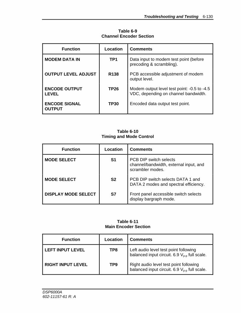
Troubleshooting and Testing 6-130
DSP6000A 602-11157-61 R: A
Table 6-9 Channel Encoder Section
Function Location Comments
MODEM DATA IN TP1 Data input to modem test point (before precoding & scrambling).
OUTPUT LEVEL ADJUST R138 PCB accessible adjustment of modem output level.
ENCODE OUTPUT LEVEL
TP26 Modem output level test point: -0.5 to -4.5 VDC, depending on channel bandwidth.
ENCODE SIGNAL OUTPUT
TP30 Encoded data output test point.
Table 6-10 Timing and Mode Control
Function Location Comments
MODE SELECT S1 PCB DIP switch selects channel/bandwidth, external input, and scrambler modes.
MODE SELECT S2 PCB DIP switch selects DATA 1 and DATA 2 modes and spectral efficiency.
DISPLAY MODE SELECT S7 Front panel accessible switch selects display bargraph mode.
Table 6-11 Main Encoder Section
Function Location Comments
LEFT INPUT LEVEL TP8 Left audio level test point following balanced input circuit. 6.9 Vp-p full scale.
RIGHT INPUT LEVEL TP9 Right audio level test point following balanced input circuit. 6.9 Vp-p full scale.
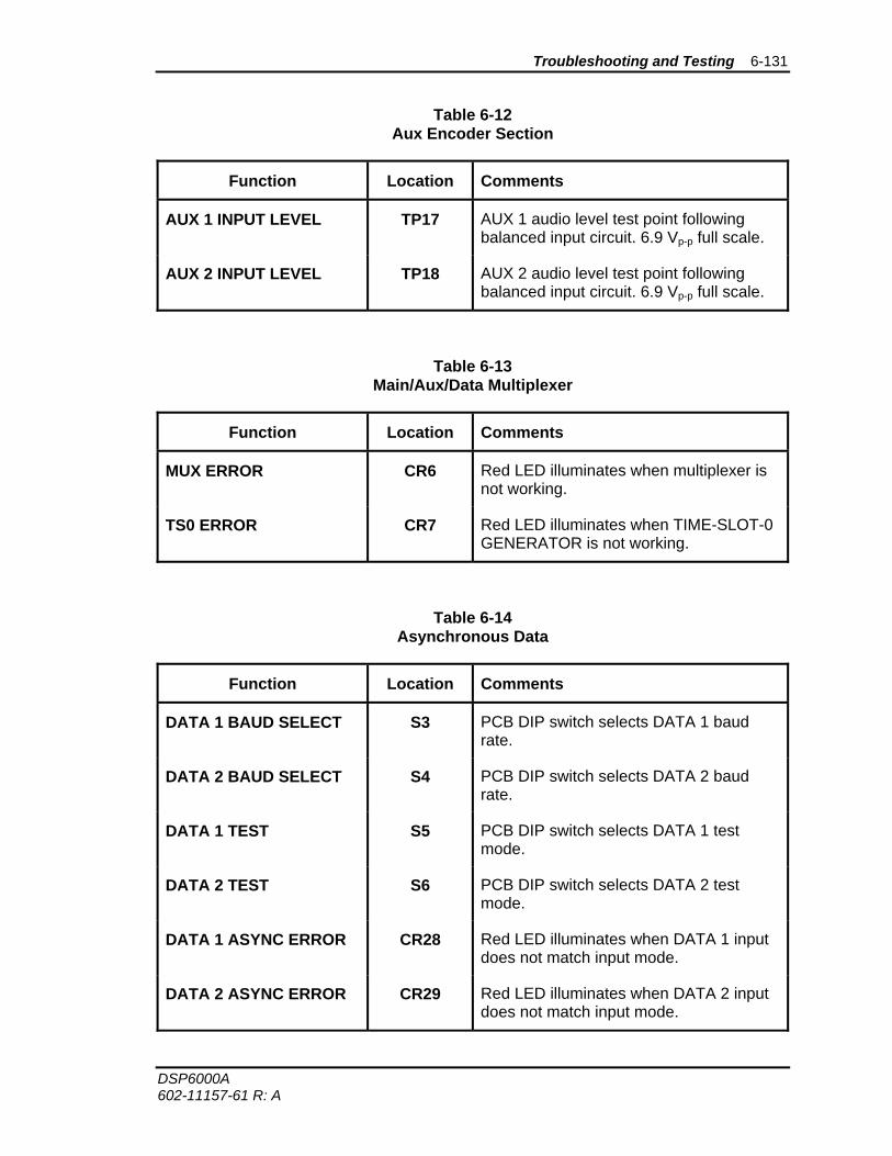
Troubleshooting and Testing 6-131
DSP6000A 602-11157-61 R: A
Table 6-12 Aux Encoder Section
Function Location Comments
AUX 1 INPUT LEVEL TP17 AUX 1 audio level test point following balanced input circuit. 6.9 Vp-p full scale.
AUX 2 INPUT LEVEL TP18 AUX 2 audio level test point following balanced input circuit. 6.9 Vp-p full scale.
Table 6-13 Main/Aux/Data Multiplexer
Function Location Comments
MUX ERROR CR6 Red LED illuminates when multiplexer is not working.
TS0 ERROR CR7 Red LED illuminates when TIME-SLOT-0 GENERATOR is not working.
Table 6-14 Asynchronous Data
Function Location Comments
DATA 1 BAUD SELECT S3 PCB DIP switch selects DATA 1 baud rate.
DATA 2 BAUD SELECT S4 PCB DIP switch selects DATA 2 baud rate.
DATA 1 TEST S5 PCB DIP switch selects DATA 1 test mode.
DATA 2 TEST S6 PCB DIP switch selects DATA 2 test mode.
DATA 1 ASYNC ERROR CR28 Red LED illuminates when DATA 1 input does not match input mode.
DATA 2 ASYNC ERROR CR29 Red LED illuminates when DATA 2 input does not match input mode.
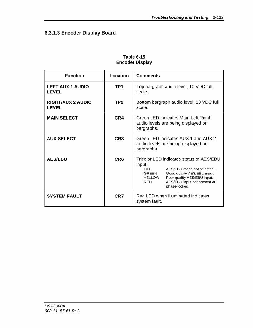
Troubleshooting and Testing 6-132
DSP6000A 602-11157-61 R: A
6.3.1.3 Encoder Display Board
Table 6-15
Encoder Display
Function Location Comments
LEFT/AUX 1 AUDIO LEVEL
TP1 Top bargraph audio level, 10 VDC full scale.
RIGHT/AUX 2 AUDIO LEVEL
TP2 Bottom bargraph audio level, 10 VDC full scale.
MAIN SELECT CR4 Green LED indicates Main Left/Right audio levels are being displayed on bargraphs.
AUX SELECT CR3 Green LED indicates AUX 1 and AUX 2 audio levels are being displayed on bargraphs.
AES/EBU CR6 Tricolor LED indicates status of AES/EBU input: OFF AES/EBU mode not selected. GREEN Good quality AES/EBU input. YELLOW Poor quality AES/EBU input. RED AES/EBU input not present or phase-locked.
SYSTEM FAULT CR7 Red LED when illuminated indicates system fault.
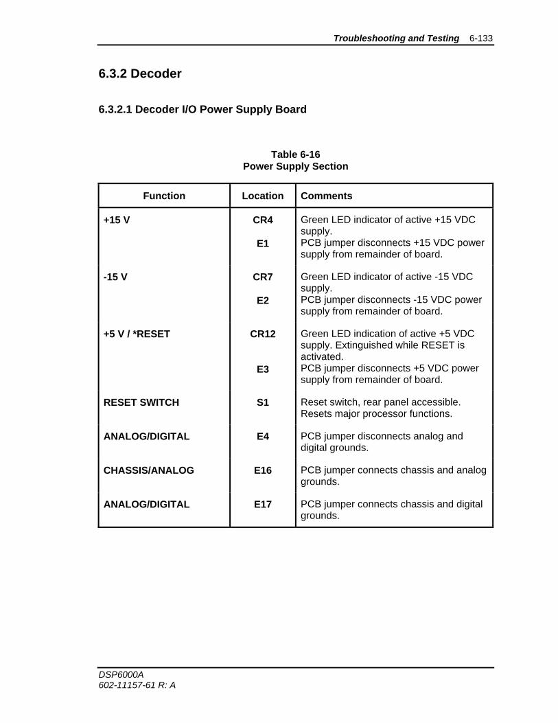
Troubleshooting and Testing 6-133
DSP6000A 602-11157-61 R: A
6.3.2 Decoder
6.3.2.1 Decoder I/O Power Supply Board
Table 6-16 Power Supply Section
Function Location Comments
+15 V CR4
E1
Green LED indicator of active +15 VDC supply. PCB jumper disconnects +15 VDC power supply from remainder of board.
-15 V CR7
E2
Green LED indicator of active -15 VDC supply. PCB jumper disconnects -15 VDC power supply from remainder of board.
+5 V / *RESET CR12
E3
Green LED indication of active +5 VDC supply. Extinguished while RESET is activated. PCB jumper disconnects +5 VDC power supply from remainder of board.
RESET SWITCH S1 Reset switch, rear panel accessible. Resets major processor functions.
ANALOG/DIGITAL E4 PCB jumper disconnects analog and digital grounds.
CHASSIS/ANALOG E16 PCB jumper connects chassis and analog grounds.
ANALOG/DIGITAL E17 PCB jumper connects chassis and digital grounds.
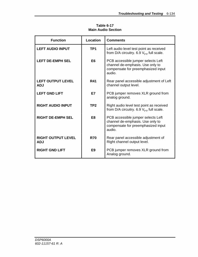
Troubleshooting and Testing 6-134
DSP6000A 602-11157-61 R: A
Table 6-17 Main Audio Section
Function Location Comments
LEFT AUDIO INPUT TP1 Left audio level test point as received from D/A circuitry. 6.9 Vp-p full scale.
LEFT DE-EMPH SEL E6 PCB accessible jumper selects Left channel de-emphasis. Use only to compensate for preemphasized input audio.
LEFT OUTPUT LEVEL ADJ
R41 Rear panel accessible adjustment of Left channel output level.
LEFT GND LIFT E7 PCB jumper removes XLR ground from analog ground.
RIGHT AUDIO INPUT TP2 Right audio level test point as received from D/A circuitry. 6.9 Vp-p full scale.
RIGHT DE-EMPH SEL E8 PCB accessible jumper selects Left channel de-emphasis. Use only to compensate for preemphasized input audio.
RIGHT OUTPUT LEVEL ADJ
R70 Rear panel accessible adjustment of Right channel output level.
RIGHT GND LIFT E9 PCB jumper removes XLR ground from Analog ground.
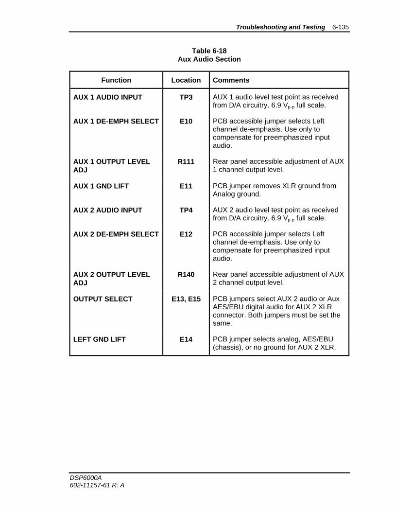
Troubleshooting and Testing 6-135
DSP6000A 602-11157-61 R: A
Table 6-18 Aux Audio Section
Function Location Comments
AUX 1 AUDIO INPUT TP3 AUX 1 audio level test point as received from D/A circuitry. 6.9 Vp-p full scale.
AUX 1 DE-EMPH SELECT E10 PCB accessible jumper selects Left channel de-emphasis. Use only to compensate for preemphasized input audio.
AUX 1 OUTPUT LEVEL ADJ
R111 Rear panel accessible adjustment of AUX 1 channel output level.
AUX 1 GND LIFT E11 PCB jumper removes XLR ground from Analog ground.
AUX 2 AUDIO INPUT TP4 AUX 2 audio level test point as received from D/A circuitry. 6.9 Vp-p full scale.
AUX 2 DE-EMPH SELECT E12 PCB accessible jumper selects Left channel de-emphasis. Use only to compensate for preemphasized input audio.
AUX 2 OUTPUT LEVEL ADJ
R140 Rear panel accessible adjustment of AUX 2 channel output level.
OUTPUT SELECT E13, E15 PCB jumpers select AUX 2 audio or Aux AES/EBU digital audio for AUX 2 XLR connector. Both jumpers must be set the same.
LEFT GND LIFT E14 PCB jumper selects analog, AES/EBU (chassis), or no ground for AUX 2 XLR.
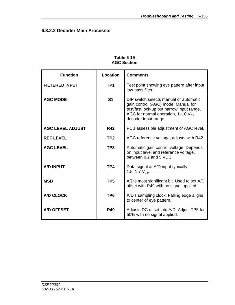
Troubleshooting and Testing 6-136
DSP6000A 602-11157-61 R: A
6.3.2.2 Decoder Main Processor
Table 6-19 AGC Section
Function Location Comments
FILTERED INPUT TP1 Test point showing eye pattern after input low-pass filter.
AGC MODE S1 DIP switch selects manual or automatic gain control (AGC) mode. Manual for test/fast lock-up but narrow input range. AGC for normal operation, 1–10 Vp-p decoder input range.
AGC LEVEL ADJUST R42 PCB assessible adjustment of AGC level.
REF LEVEL TP2 AGC reference voltage, adjusts with R42.
AGC LEVEL TP3 Automatic gain control voltage. Depends on input level and reference voltage, between 0.2 and 5 VDC.
A/D INPUT TP4 Data signal at A/D input typically 1.5–1.7 Vp-p.
MSB TP5 A/D's most significant bit. Used to set A/D offset with R49 with no signal applied.
A/D CLOCK TP6 A/D's sampling clock. Falling edge aligns to center of eye pattern.
A/D OFFSET R49 Adjusts DC offset into A/D. Adjust TP5 for 50% with no signal applied.
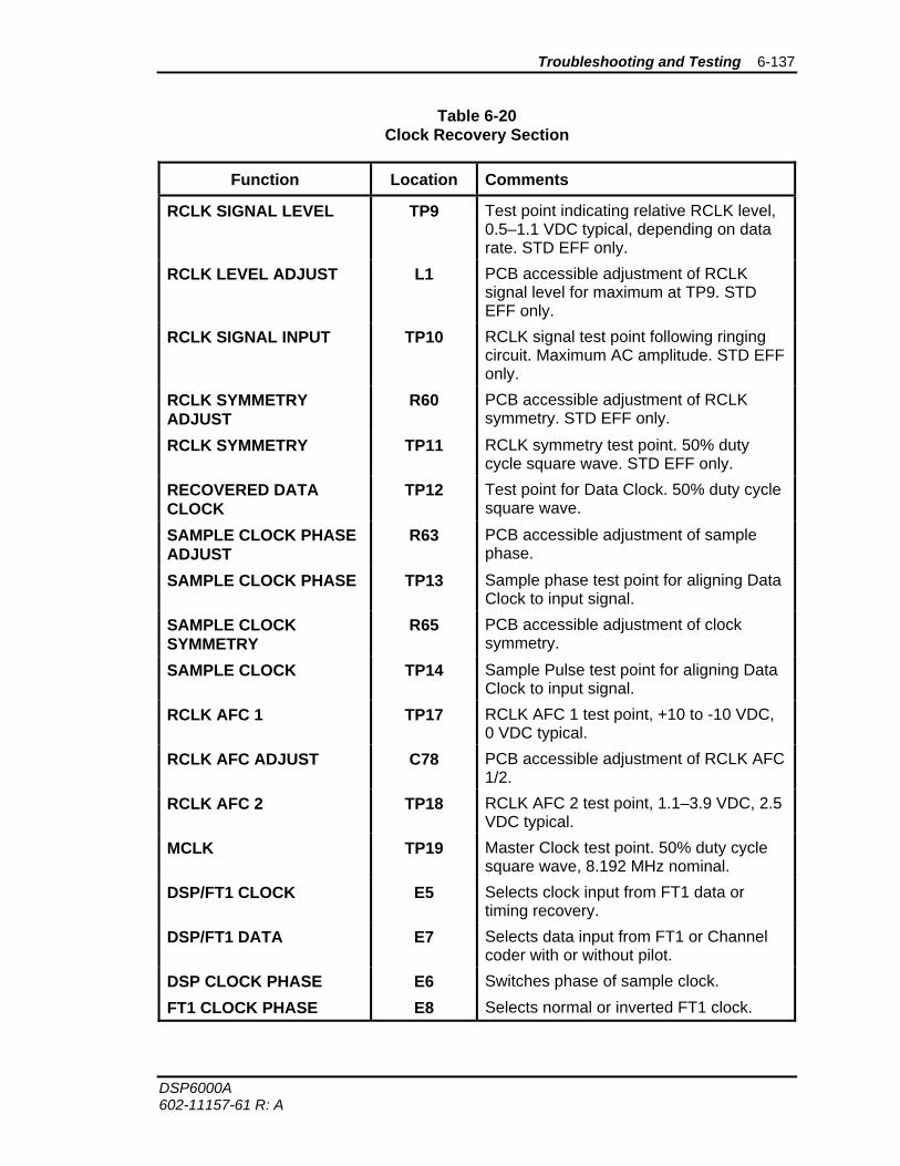
Troubleshooting and Testing 6-137
DSP6000A 602-11157-61 R: A
Table 6-20 Clock Recovery Section
Function Location Comments
RCLK SIGNAL LEVEL TP9 Test point indicating relative RCLK level, 0.5–1.1 VDC typical, depending on data rate. STD EFF only.
RCLK LEVEL ADJUST L1 PCB accessible adjustment of RCLK signal level for maximum at TP9. STD EFF only.
RCLK SIGNAL INPUT TP10 RCLK signal test point following ringing circuit. Maximum AC amplitude. STD EFF only.
RCLK SYMMETRY ADJUST
R60 PCB accessible adjustment of RCLK symmetry. STD EFF only.
RCLK SYMMETRY TP11 RCLK symmetry test point. 50% duty cycle square wave. STD EFF only.
RECOVERED DATA CLOCK
TP12 Test point for Data Clock. 50% duty cycle square wave.
SAMPLE CLOCK PHASE ADJUST
R63 PCB accessible adjustment of sample phase.
SAMPLE CLOCK PHASE TP13 Sample phase test point for aligning Data Clock to input signal.
SAMPLE CLOCK SYMMETRY
R65 PCB accessible adjustment of clock symmetry.
SAMPLE CLOCK TP14 Sample Pulse test point for aligning Data Clock to input signal.
RCLK AFC 1 TP17 RCLK AFC 1 test point, +10 to -10 VDC, 0 VDC typical.
RCLK AFC ADJUST C78 PCB accessible adjustment of RCLK AFC 1/2.
RCLK AFC 2 TP18 RCLK AFC 2 test point, 1.1–3.9 VDC, 2.5 VDC typical.
MCLK TP19 Master Clock test point. 50% duty cycle square wave, 8.192 MHz nominal.
DSP/FT1 CLOCK E5 Selects clock input from FT1 data or timing recovery.
DSP/FT1 DATA E7 Selects data input from FT1 or Channel coder with or without pilot.
DSP CLOCK PHASE E6 Switches phase of sample clock. FT1 CLOCK PHASE E8 Selects normal or inverted FT1 clock.
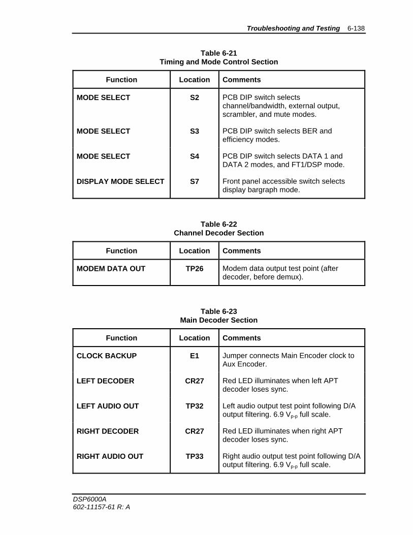
Troubleshooting and Testing 6-138
DSP6000A 602-11157-61 R: A
Table 6-21 Timing and Mode Control Section
Function Location Comments
MODE SELECT S2 PCB DIP switch selects channel/bandwidth, external output, scrambler, and mute modes.
MODE SELECT S3 PCB DIP switch selects BER and efficiency modes.
MODE SELECT S4 PCB DIP switch selects DATA 1 and DATA 2 modes, and FT1/DSP mode.
DISPLAY MODE SELECT S7 Front panel accessible switch selects display bargraph mode.
Table 6-22 Channel Decoder Section
Function Location Comments
MODEM DATA OUT TP26 Modem data output test point (after decoder, before demux).
Table 6-23 Main Decoder Section
Function Location Comments
CLOCK BACKUP E1 Jumper connects Main Encoder clock to Aux Encoder.
LEFT DECODER CR27 Red LED illuminates when left APT decoder loses sync.
LEFT AUDIO OUT TP32 Left audio output test point following D/A output filtering. 6.9 Vp-p full scale.
RIGHT DECODER CR27 Red LED illuminates when right APT decoder loses sync.
RIGHT AUDIO OUT TP33 Right audio output test point following D/A output filtering. 6.9 Vp-p full scale.
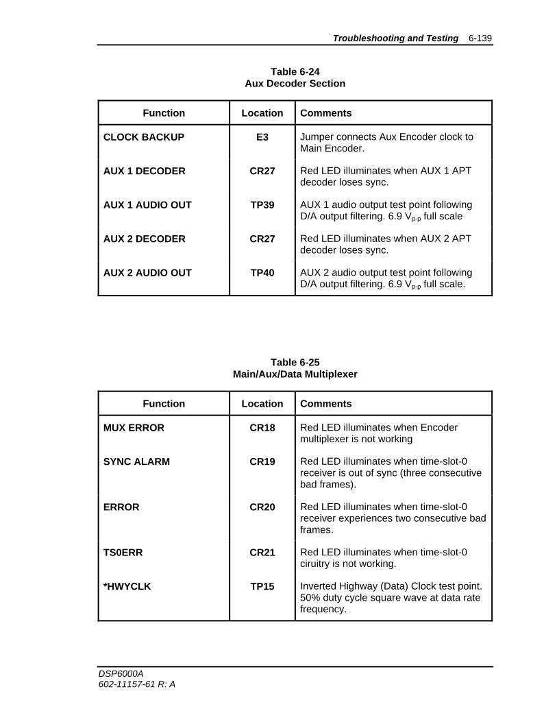
Troubleshooting and Testing 6-139
DSP6000A 602-11157-61 R: A
Table 6-24 Aux Decoder Section
Function Location Comments
CLOCK BACKUP E3 Jumper connects Aux Encoder clock to Main Encoder.
AUX 1 DECODER CR27 Red LED illuminates when AUX 1 APT decoder loses sync.
AUX 1 AUDIO OUT TP39 AUX 1 audio output test point following D/A output filtering. 6.9 Vp-p full scale
AUX 2 DECODER CR27 Red LED illuminates when AUX 2 APT decoder loses sync.
AUX 2 AUDIO OUT TP40 AUX 2 audio output test point following D/A output filtering. 6.9 Vp-p full scale.
Table 6-25 Main/Aux/Data Multiplexer
Function Location Comments
MUX ERROR CR18 Red LED illuminates when Encoder multiplexer is not working
SYNC ALARM CR19 Red LED illuminates when time-slot-0 receiver is out of sync (three consecutive bad frames).
ERROR CR20 Red LED illuminates when time-slot-0 receiver experiences two consecutive bad frames.
TS0ERR CR21 Red LED illuminates when time-slot-0 ciruitry is not working.
*HWYCLK TP15 Inverted Highway (Data) Clock test point. 50% duty cycle square wave at data rate frequency.
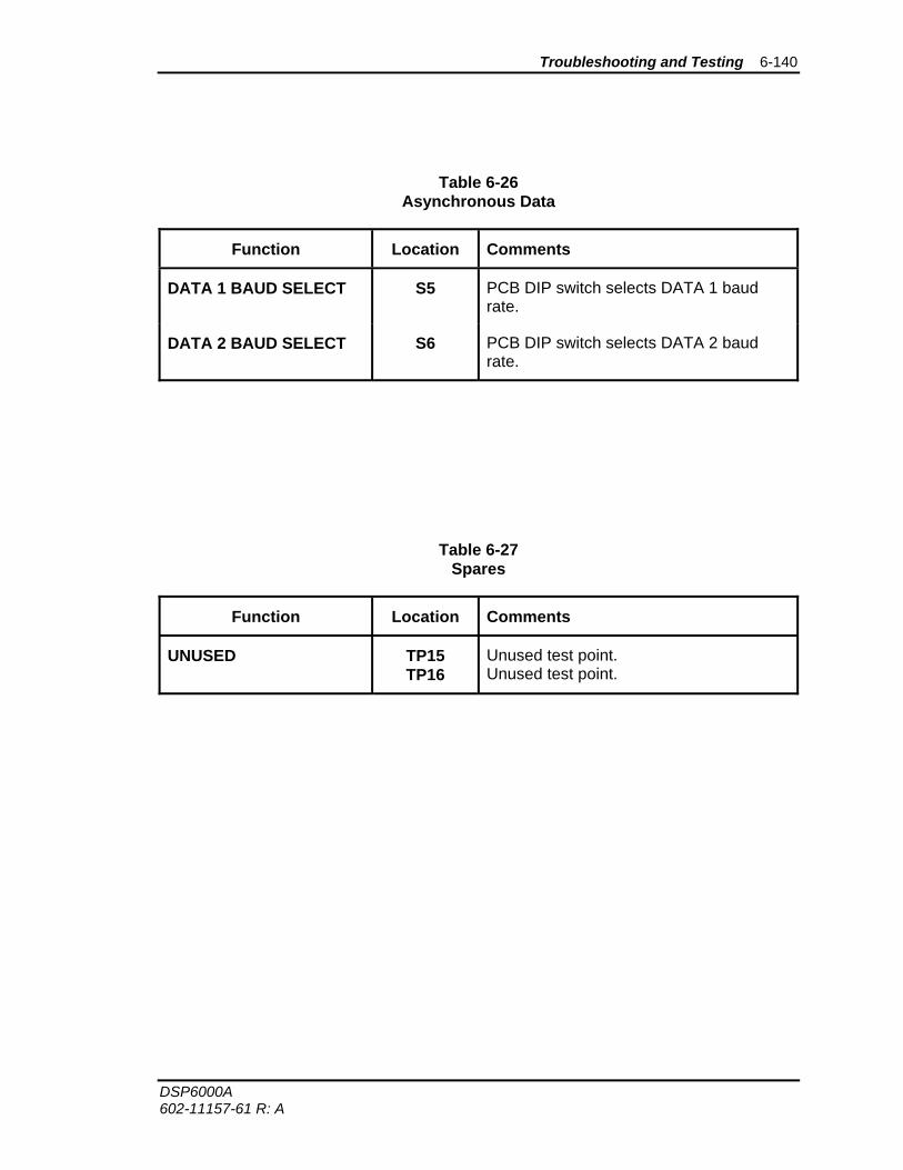
Troubleshooting and Testing 6-140
DSP6000A 602-11157-61 R: A
Table 6-26 Asynchronous Data
Function Location Comments
DATA 1 BAUD SELECT S5 PCB DIP switch selects DATA 1 baud rate.
DATA 2 BAUD SELECT S6 PCB DIP switch selects DATA 2 baud rate.
Table 6-27 Spares
Function Location Comments
UNUSED TP15 TP16
Unused test point. Unused test point.
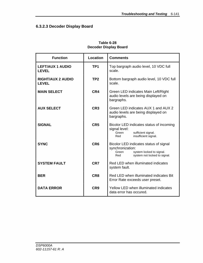
Troubleshooting and Testing 6-141
DSP6000A 602-11157-61 R: A
6.3.2.3 Decoder Display Board
Table 6-28 Decoder Display Board
Function Location Comments
LEFT/AUX 1 AUDIO LEVEL
TP1 Top bargraph audio level, 10 VDC full scale.
RIGHT/AUX 2 AUDIO LEVEL
TP2 Bottom bargraph audio level, 10 VDC full scale.
MAIN SELECT CR4 Green LED indicates Main Left/Right audio levels are being displayed on bargraphs.
AUX SELECT CR3 Green LED indicates AUX 1 and AUX 2 audio levels are being displayed on bargraphs.
SIGNAL CR5 Bicolor LED indicates status of incoming signal level: Green sufficient signal. Red insufficient signal.
SYNC CR6 Bicolor LED indicates status of signal synchronization: Green system locked to signal. Red system not locked to signal.
SYSTEM FAULT CR7 Red LED when illuminated indicates system fault.
BER CR8 Red LED when illuminated indicates Bit Error Rate exceeds user preset.
DATA ERROR CR9 Yellow LED when illuminated indicates data error has occured.
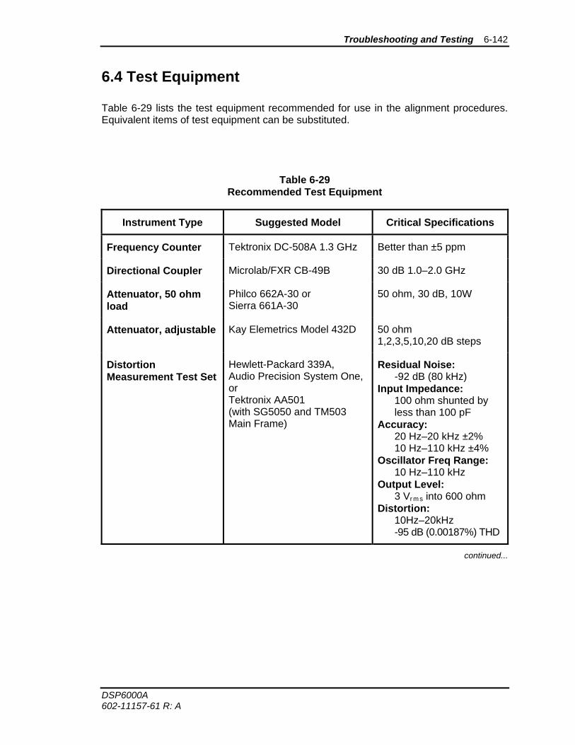
Troubleshooting and Testing 6-142
DSP6000A 602-11157-61 R: A
6.4 Test Equipment
Table 6-29 lists the test equipment recommended for use in the alignment procedures. Equivalent items of test equipment can be substituted.
Table 6-29 Recommended Test Equipment
Instrument Type Suggested Model Critical Specifications
Frequency Counter Tektronix DC-508A 1.3 GHz Better than ±5 ppm
Directional Coupler Microlab/FXR CB-49B 30 dB 1.0–2.0 GHz
Attenuator, 50 ohm load
Philco 662A-30 or Sierra 661A-30
50 ohm, 30 dB, 10W
Attenuator, adjustable Kay Elemetrics Model 432D 50 ohm 1,2,3,5,10,20 dB steps
Distortion Measurement Test Set
Hewlett-Packard 339A, Audio Precision System One, or Tektronix AA501 (with SG5050 and TM503 Main Frame)
Residual Noise: -92 dB (80 kHz) Input Impedance: 100 ohm shunted by less than 100 pF Accuracy: 20 Hz–20 kHz ±2% 10 Hz–110 kHz ±4% Oscillator Freq Range: 10 Hz–110 kHz Output Level: 3 Vr m s into 600 ohm Distortion: 10Hz–20kHz -95 dB (0.00187%) THD
continued...
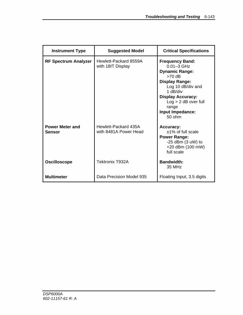
Troubleshooting and Testing 6-143
DSP6000A 602-11157-61 R: A
Instrument Type Suggested Model Critical Specifications
RF Spectrum Analyzer Hewlett-Packard 8559A with 18IT Display
Frequency Band: 0.01–3 GHz Dynamic Range: >70 dB Display Range: Log 10 dB/div and 1 dB/div Display Accuracy: Log > 2 dB over full range Input Impedance: 50 ohm
Power Meter and Sensor
Hewlett-Packard 435A with 8481A Power Head
Accuracy: ±1% of full scale Power Range: -25 dBm (3 uW) to +20 dBm (100 mW) full scale
Oscilloscope Tektronix T932A Bandwidth: 35 MHz
Multimeter Data Precision Model 935 Floating Input, 3.5 digits
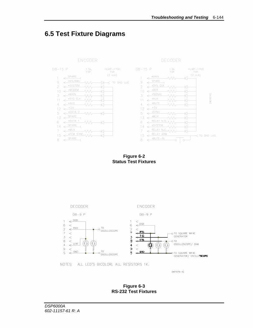
Troubleshooting and Testing 6-144
DSP6000A 602-11157-61 R: A
6.5 Test Fixture Diagrams
Figure 6-2 Status Test Fixtures
Figure 6-3 RS-232 Test Fixtures
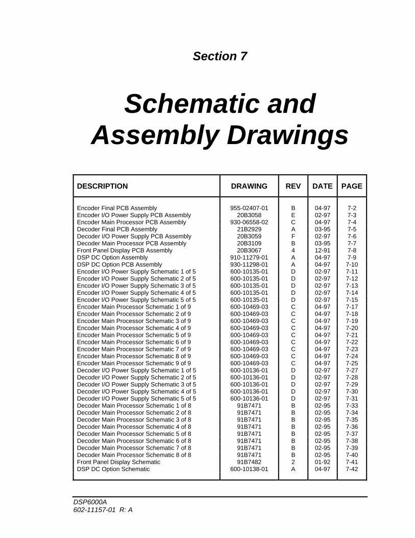
DSP6000A 602-11157-01 R: A
Section 7
Schematic and Assembly Drawings
DESCRIPTION DRAWING REV DATE PAGE
Encoder Final PCB Assembly 955-02407-01 B 04-97 7-2 Encoder I/O Power Supply PCB Assembly 20B3058 E 02-97 7-3 Encoder Main Processor PCB Assembly 930-06558-02 C 04-97 7-4 Decoder Final PCB Assembly 21B2929 A 03-95 7-5 Decoder I/O Power Supply PCB Assembly 20B3059 F 02-97 7-6 Decoder Main Processor PCB Assembly 20B3109 B 03-95 7-7 Front Panel Display PCB Assembly 20B3067 4 12-91 7-8 DSP DC Option Assembly 910-11279-01 A 04-97 7-9 DSP DC Option PCB Assembly 930-11298-01 A 04-97 7-10 Encoder I/O Power Supply Schematic 1 of 5 600-10135-01 D 02-97 7-11 Encoder I/O Power Supply Schematic 2 of 5 600-10135-01 D 02-97 7-12 Encoder I/O Power Supply Schematic 3 of 5 600-10135-01 D 02-97 7-13 Encoder I/O Power Supply Schematic 4 of 5 600-10135-01 D 02-97 7-14 Encoder I/O Power Supply Schematic 5 of 5 600-10135-01 D 02-97 7-15 Encoder Main Processor Schematic 1 of 9 600-10469-03 C 04-97 7-17 Encoder Main Processor Schematic 2 of 9 600-10469-03 C 04-97 7-18 Encoder Main Processor Schematic 3 of 9 600-10469-03 C 04-97 7-19 Encoder Main Processor Schematic 4 of 9 600-10469-03 C 04-97 7-20 Encoder Main Processor Schematic 5 of 9 600-10469-03 C 04-97 7-21 Encoder Main Processor Schematic 6 of 9 600-10469-03 C 04-97 7-22 Encoder Main Processor Schematic 7 of 9 600-10469-03 C 04-97 7-23 Encoder Main Processor Schematic 8 of 9 600-10469-03 C 04-97 7-24 Encoder Main Processor Schematic 9 of 9 600-10469-03 C 04-97 7-25 Decoder I/O Power Supply Schematic 1 of 5 600-10136-01 D 02-97 7-27 Decoder I/O Power Supply Schematic 2 of 5 600-10136-01 D 02-97 7-28 Decoder I/O Power Supply Schematic 3 of 5 600-10136-01 D 02-97 7-29 Decoder I/O Power Supply Schematic 4 of 5 600-10136-01 D 02-97 7-30 Decoder I/O Power Supply Schematic 5 of 5 600-10136-01 D 02-97 7-31 Decoder Main Processor Schematic 1 of 8 91B7471 B 02-95 7-33 Decoder Main Processor Schematic 2 of 8 91B7471 B 02-95 7-34 Decoder Main Processor Schematic 3 of 8 91B7471 B 02-95 7-35 Decoder Main Processor Schematic 4 of 8 91B7471 B 02-95 7-36 Decoder Main Processor Schematic 5 of 8 91B7471 B 02-95 7-37 Decoder Main Processor Schematic 6 of 8 91B7471 B 02-95 7-38 Decoder Main Processor Schematic 7 of 8 91B7471 B 02-95 7-39 Decoder Main Processor Schematic 8 of 8 91B7471 B 02-95 7-40 Front Panel Display Schematic 91B7482 2 01-92 7-41 DSP DC Option Schematic 600-10138-01 A 04-97 7-42
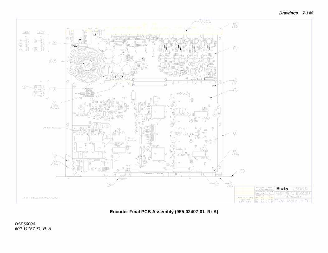
Drawings 7-146
DSP6000A 602-11157-71 R: A
Encoder Final PCB Assembly (955-02407-01 R: A)
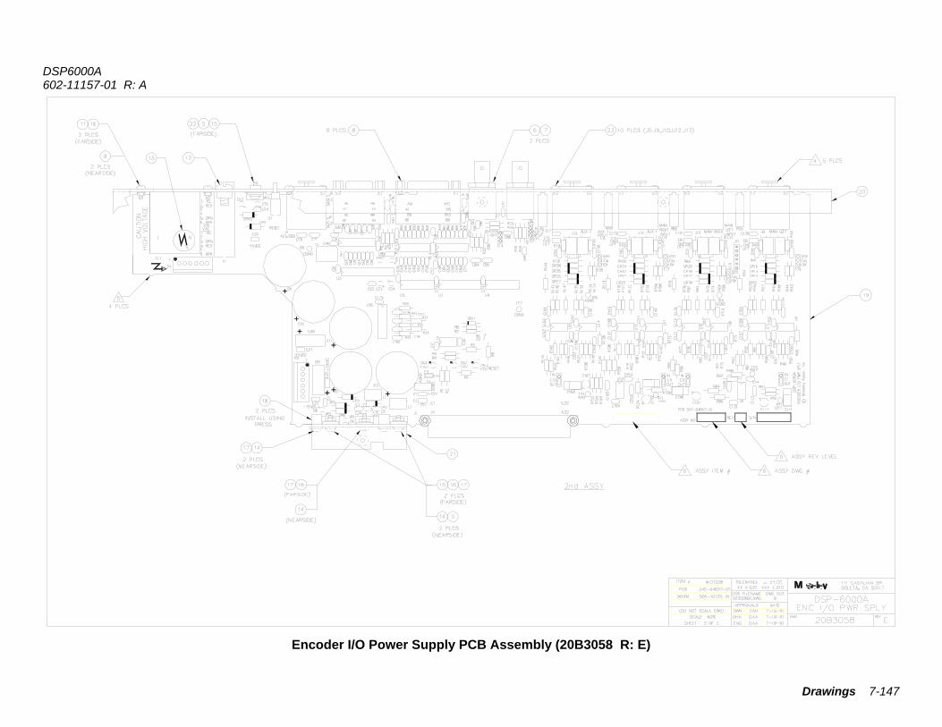
DSP6000A 602-11157-01 R: A
Drawings 7-147
Encoder I/O Power Supply PCB Assembly (20B3058 R: E)
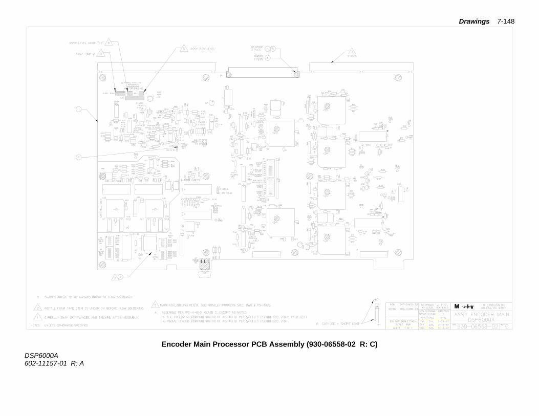
Drawings 7-148
DSP6000A 602-11157-01 R: A
Encoder Main Processor PCB Assembly (930-06558-02 R: C)
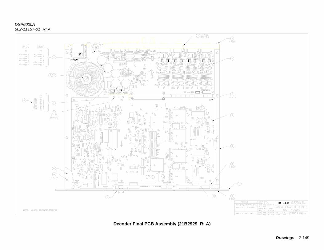
DSP6000A 602-11157-01 R: A
Drawings 7-149
Decoder Final PCB Assembly (21B2929 R: A)
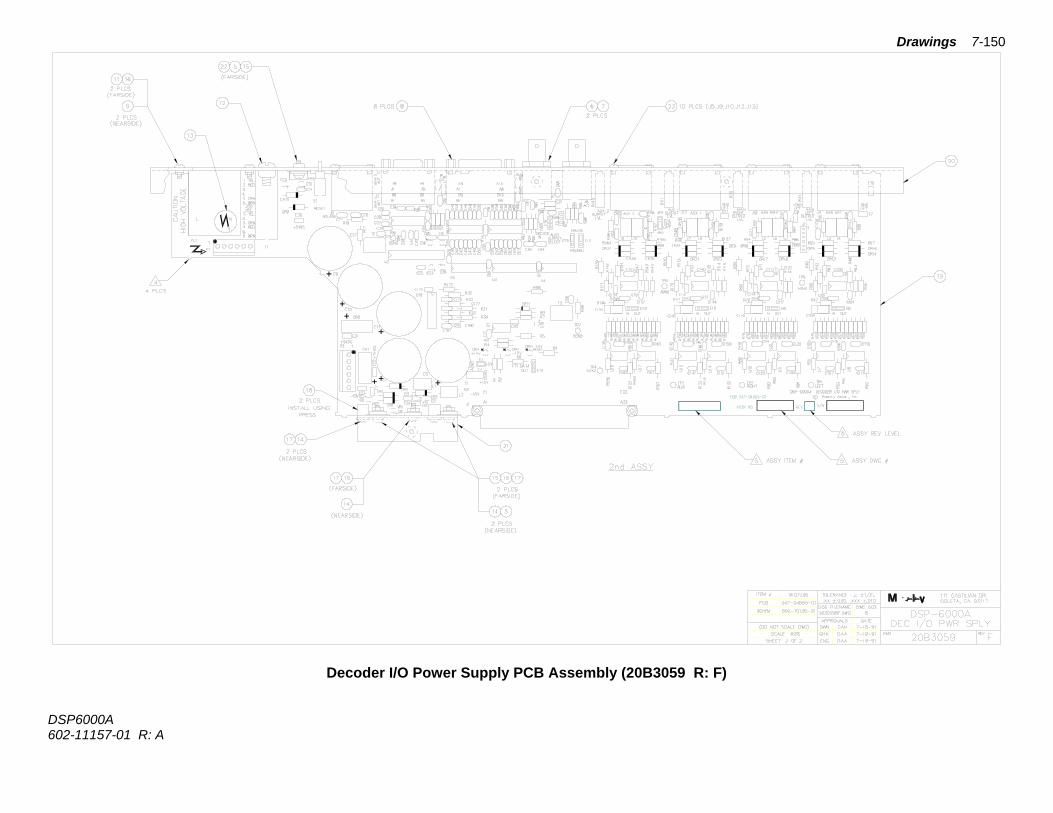
Drawings 7-150
DSP6000A 602-11157-01 R: A
Decoder I/O Power Supply PCB Assembly (20B3059 R: F)
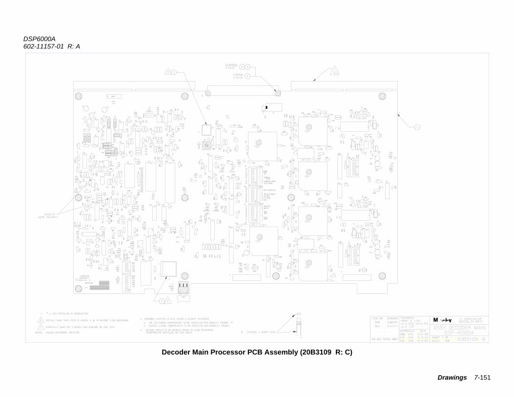
DSP6000A 602-11157-01 R: A
Drawings 7-151
Decoder Main Processor PCB Assembly (20B3109 R: C)
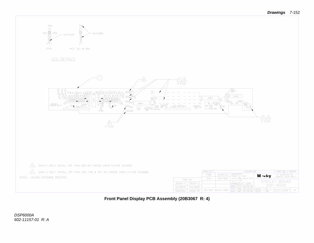
Drawings 7-152
DSP6000A 602-11157-01 R: A
Front Panel Display PCB Assembly (20B3067 R: 4)
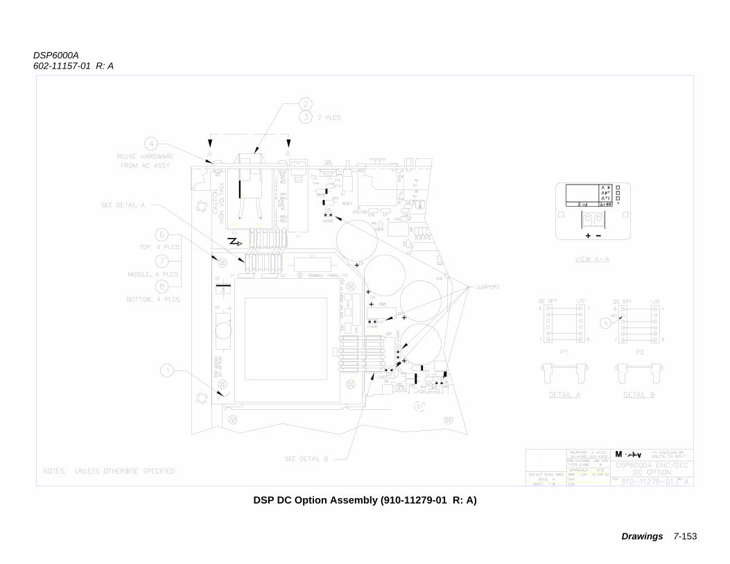
DSP6000A 602-11157-01 R: A
Drawings 7-153
DSP DC Option Assembly (910-11279-01 R: A)
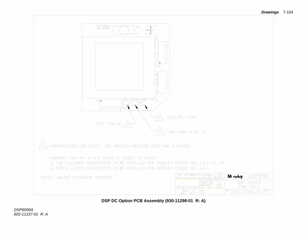
Drawings 7-154
DSP6000A 602-11157-01 R: A
DSP DC Option PCB Assembly (930-11298-01 R: A)
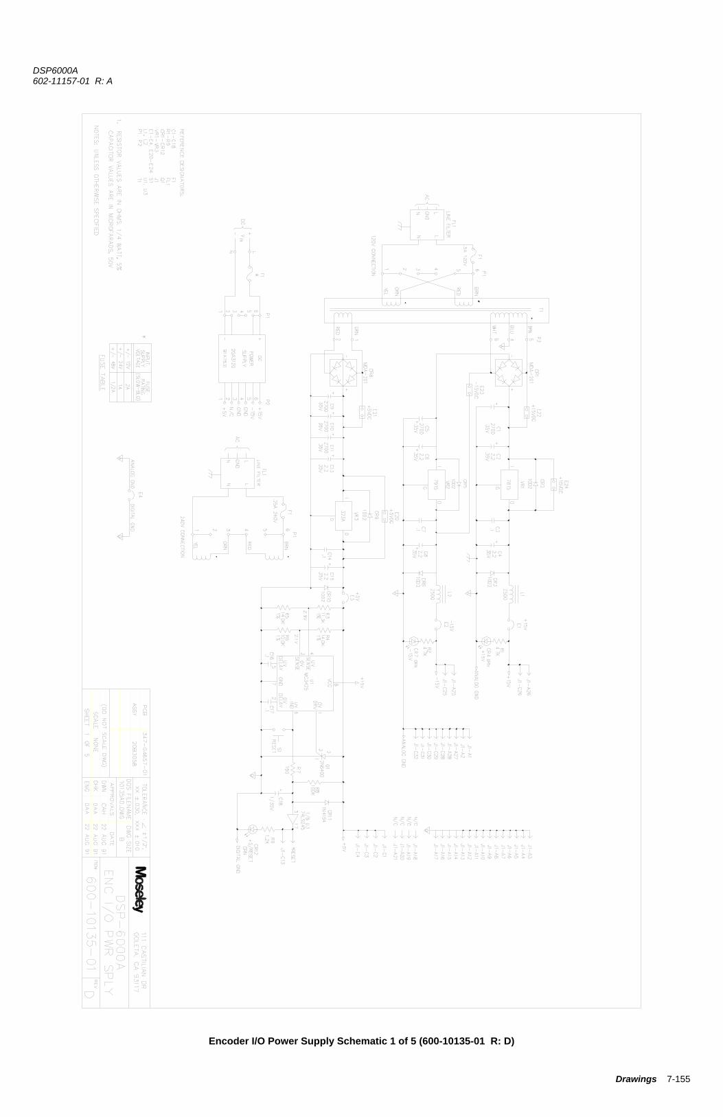
DSP6000A 602-11157-01 R: A
Drawings 7-155
Encoder I/O Power Supply Schematic 1 of 5 (600-10135-01 R: D)

DSP6000A 602-11157-01 R: A
Drawings 7-156
Encoder I/O Power Supply Schematic 2 of 5 (600-10135-01 R: D)
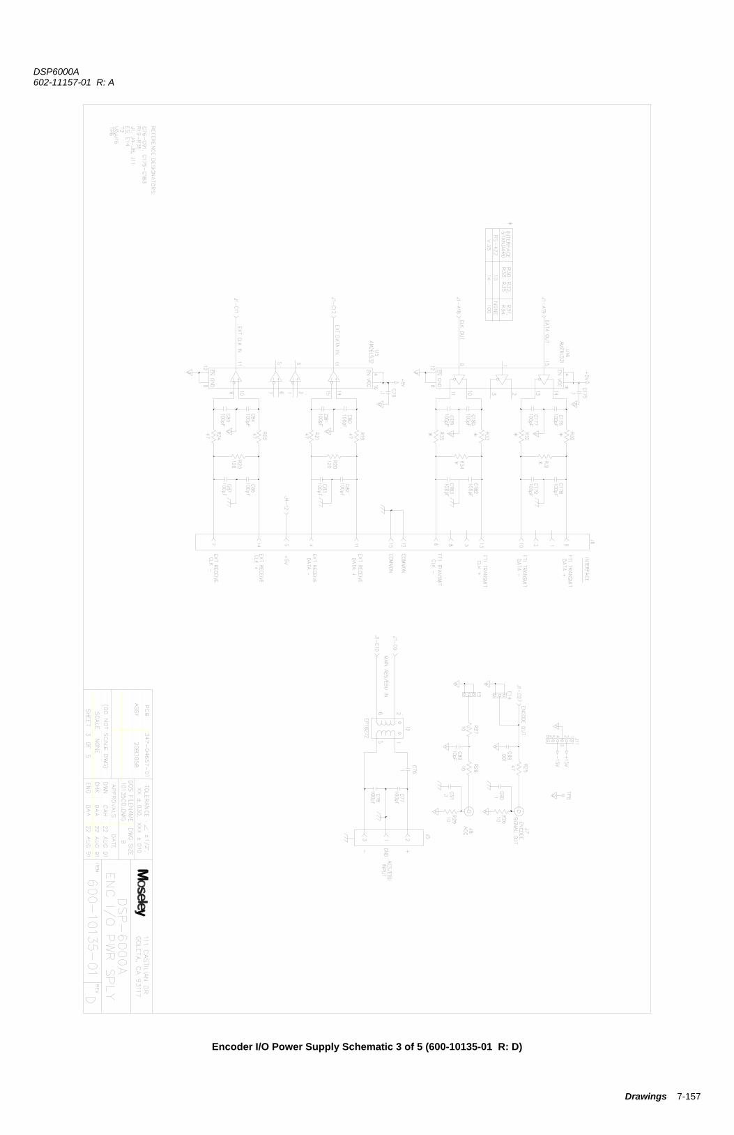
DSP6000A 602-11157-01 R: A
Drawings 7-157
Encoder I/O Power Supply Schematic 3 of 5 (600-10135-01 R: D)
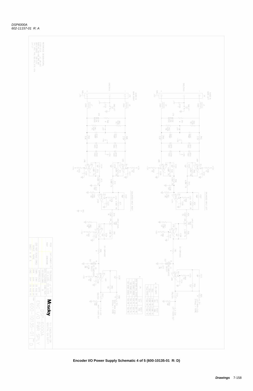
DSP6000A 602-11157-01 R: A
Drawings 7-158
Encoder I/O Power Supply Schematic 4 of 5 (600-10135-01 R: D)
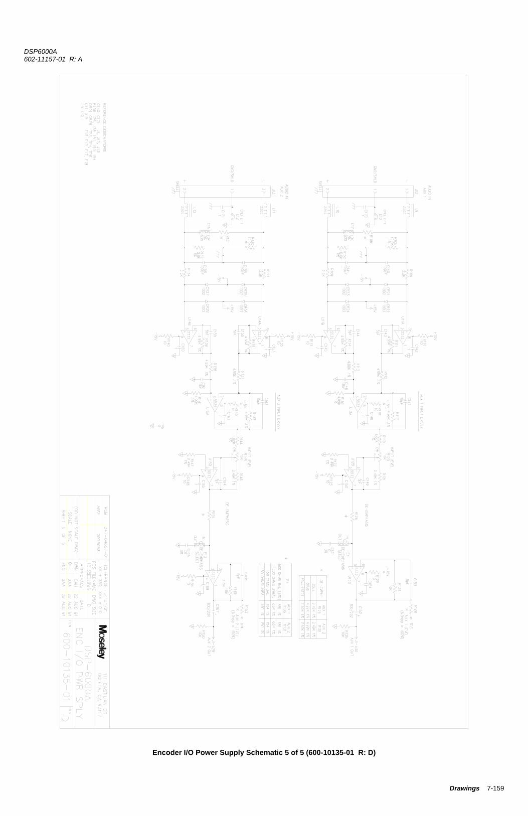
DSP6000A 602-11157-01 R: A
Drawings 7-159
Encoder I/O Power Supply Schematic 5 of 5 (600-10135-01 R: D)

DSP6000A 602-11157-01 R: A
Drawings 7-160
This page is intentionally blank.
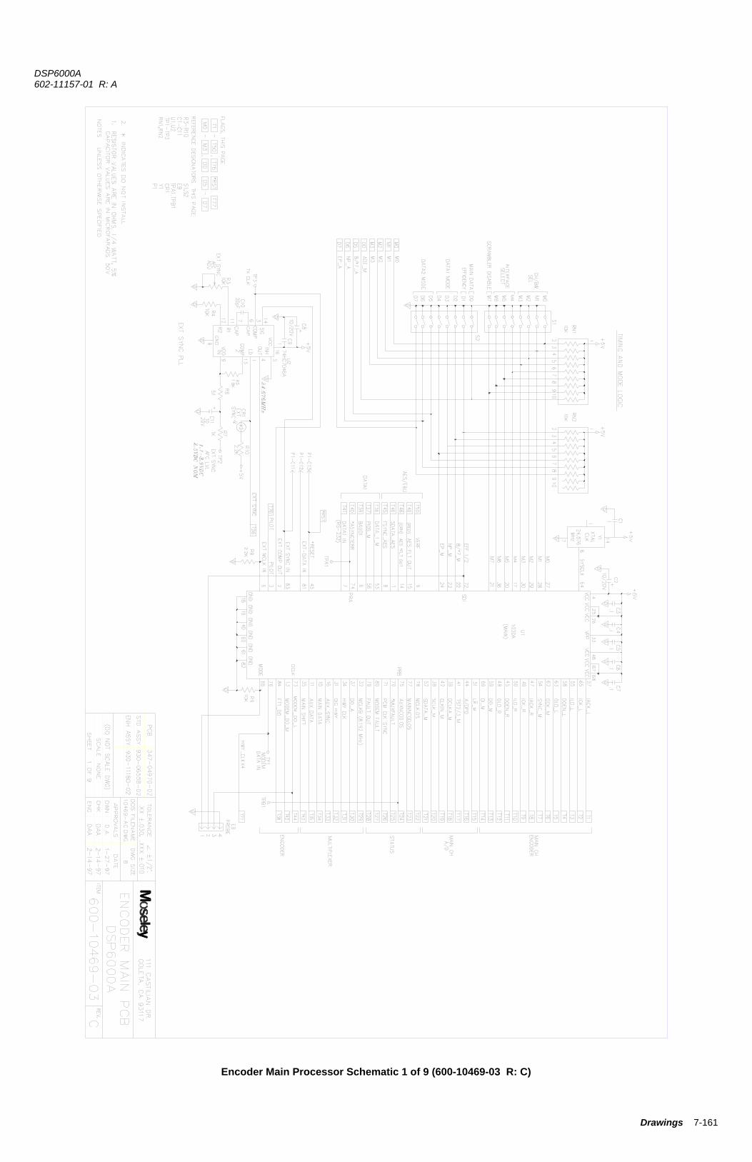
DSP6000A 602-11157-01 R: A
Drawings 7-161
Encoder Main Processor Schematic 1 of 9 (600-10469-03 R: C)
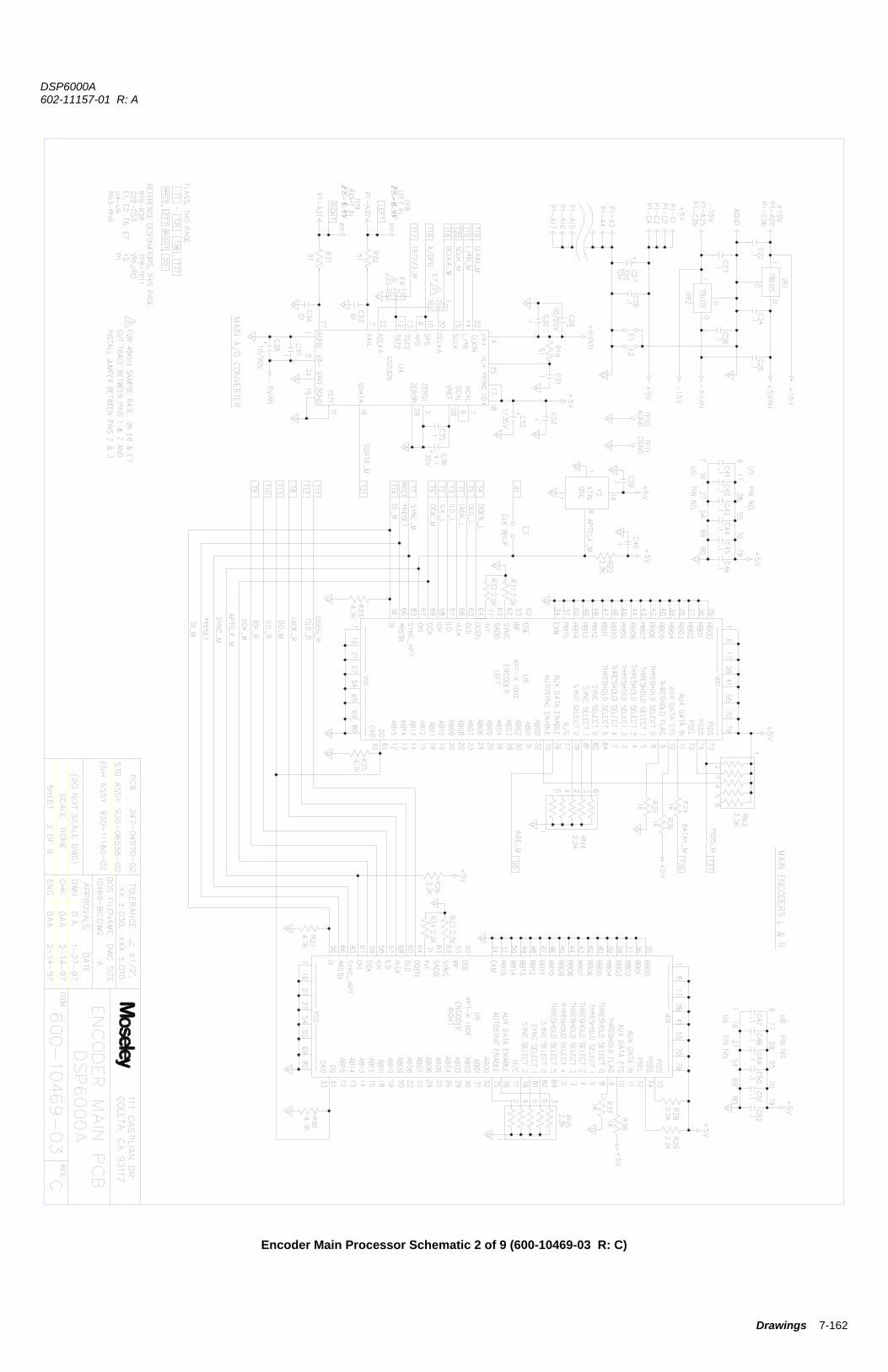
DSP6000A 602-11157-01 R: A
Drawings 7-162
Encoder Main Processor Schematic 2 of 9 (600-10469-03 R: C)
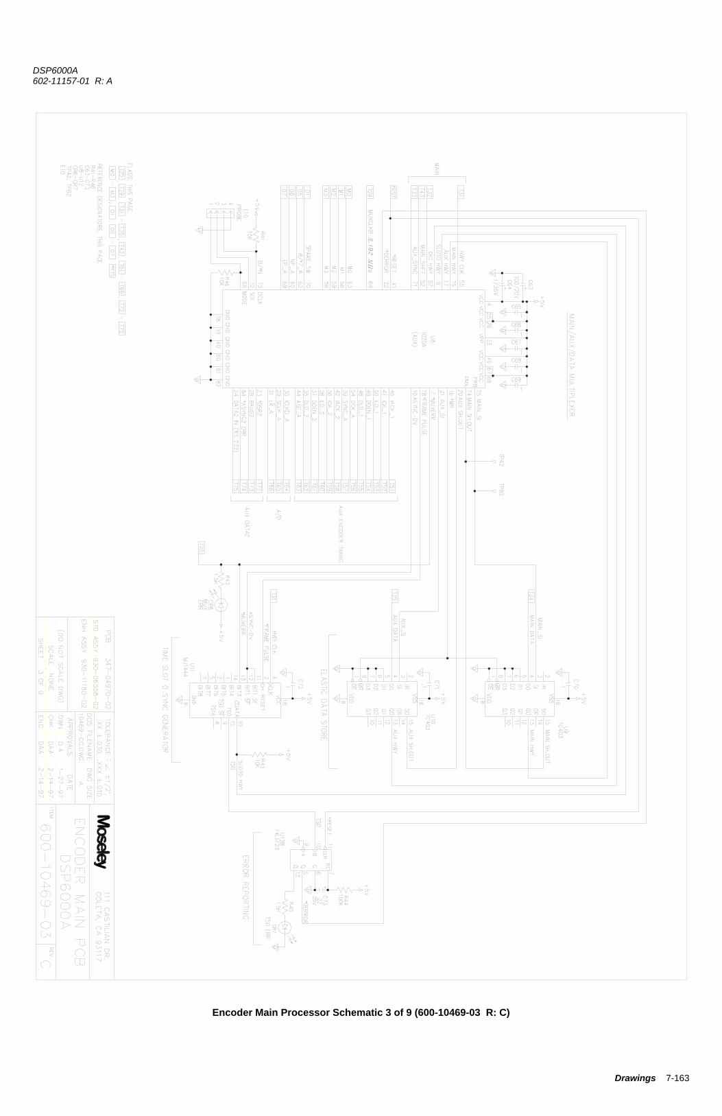
DSP6000A 602-11157-01 R: A
Drawings 7-163
Encoder Main Processor Schematic 3 of 9 (600-10469-03 R: C)
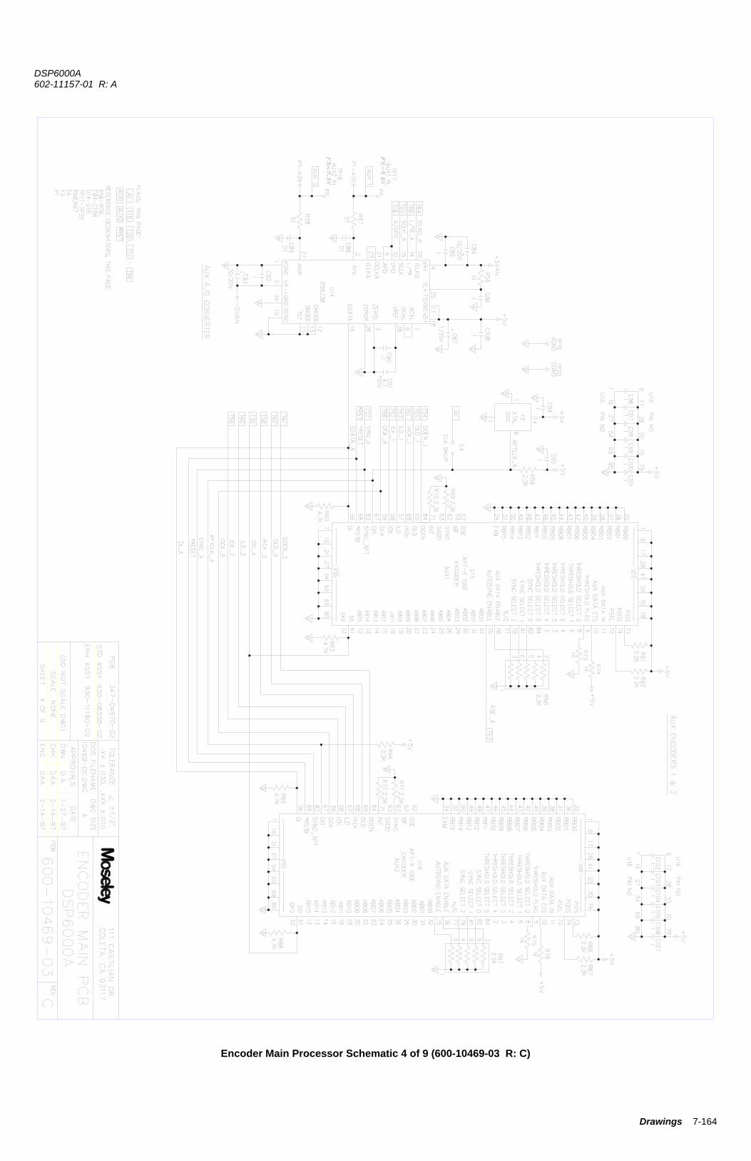
DSP6000A 602-11157-01 R: A
Drawings 7-164
Encoder Main Processor Schematic 4 of 9 (600-10469-03 R: C)
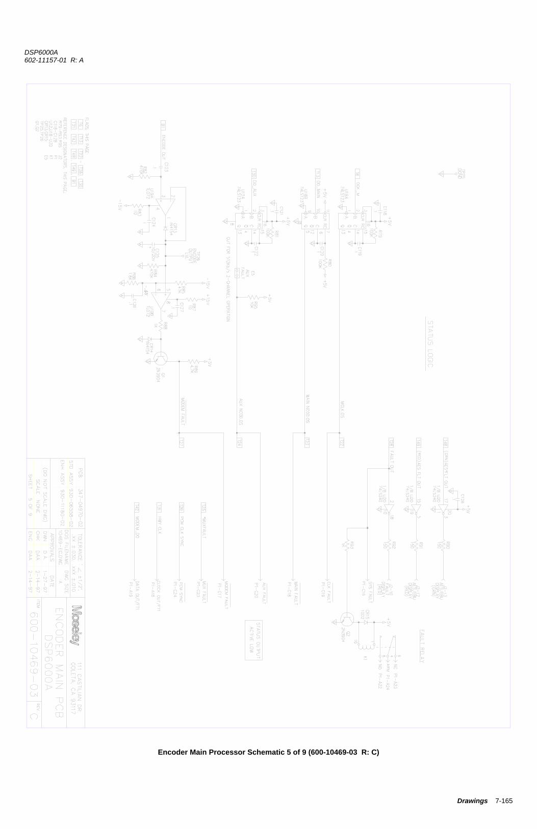
DSP6000A 602-11157-01 R: A
Drawings 7-165
Encoder Main Processor Schematic 5 of 9 (600-10469-03 R: C)
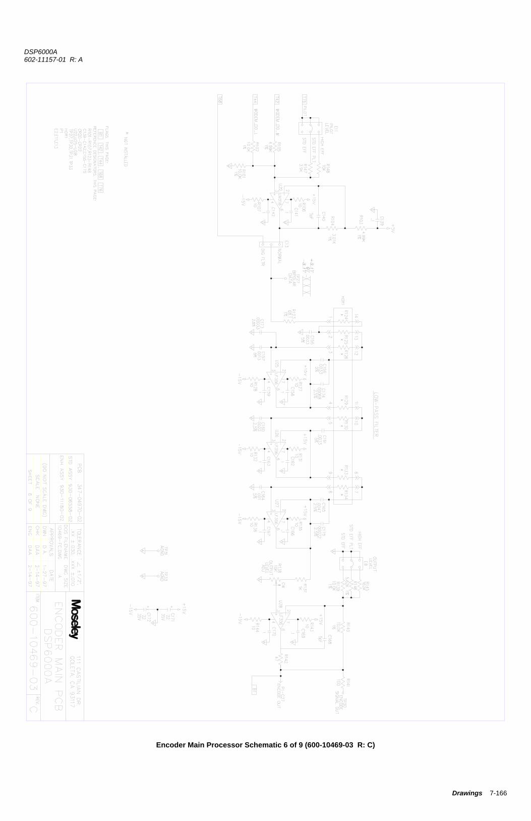
DSP6000A 602-11157-01 R: A
Drawings 7-166
Encoder Main Processor Schematic 6 of 9 (600-10469-03 R: C)
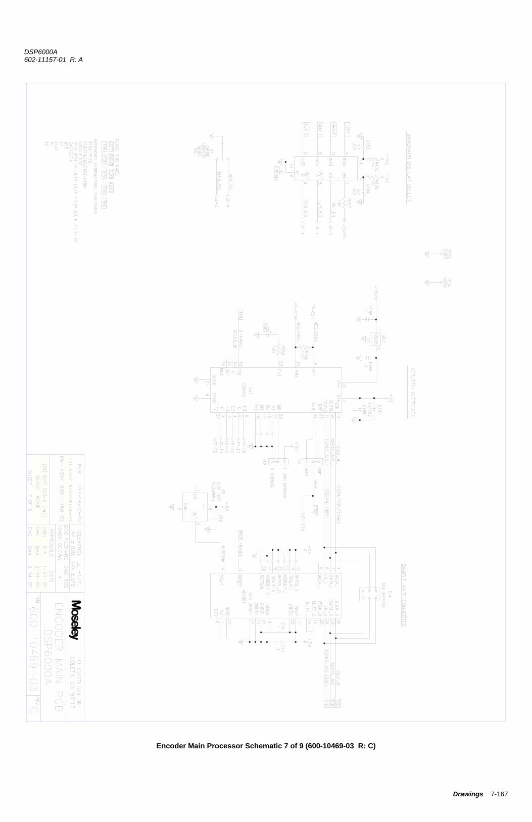
DSP6000A 602-11157-01 R: A
Drawings 7-167
Encoder Main Processor Schematic 7 of 9 (600-10469-03 R: C)
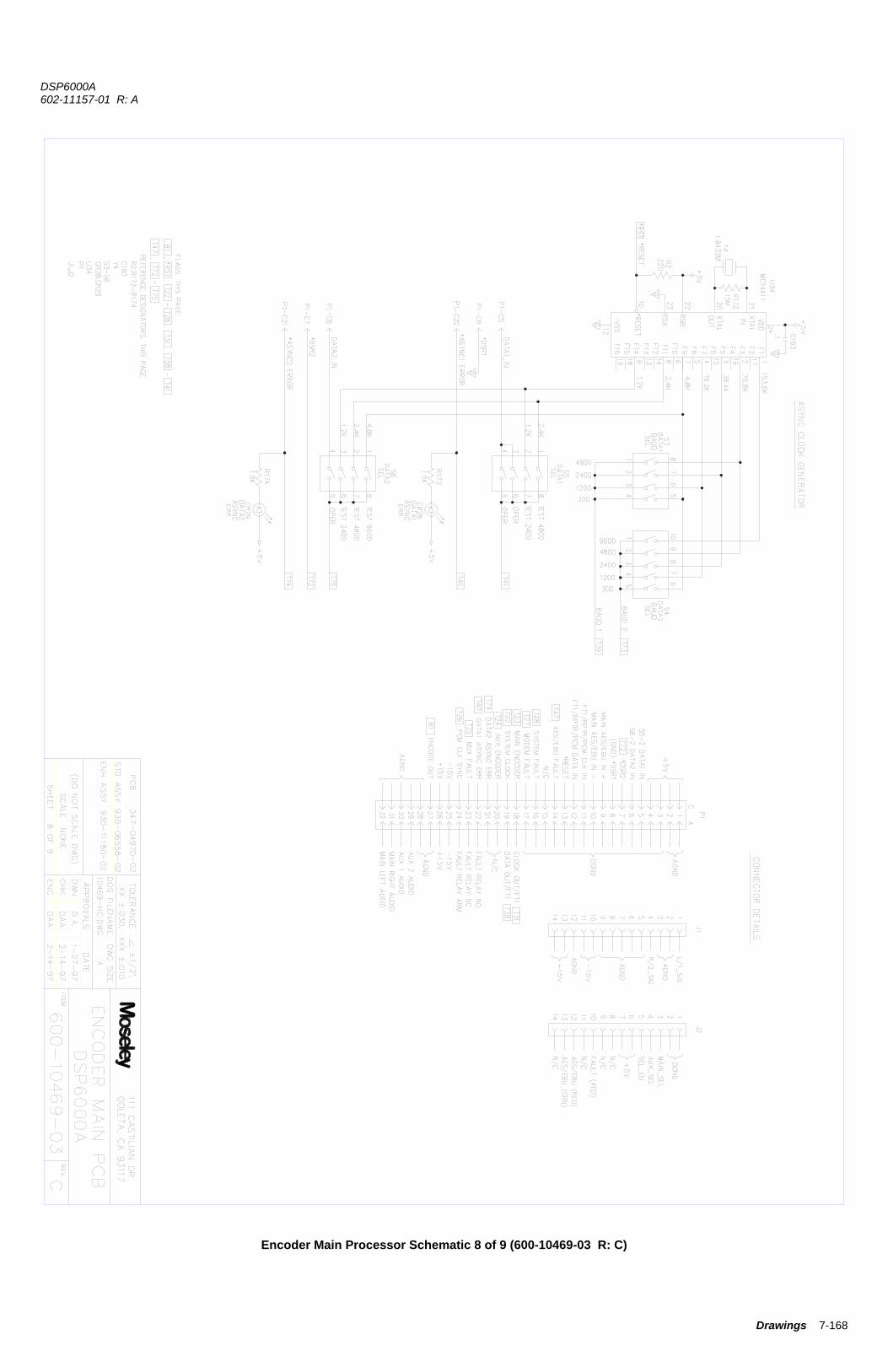
DSP6000A 602-11157-01 R: A
Drawings 7-168
Encoder Main Processor Schematic 8 of 9 (600-10469-03 R: C)
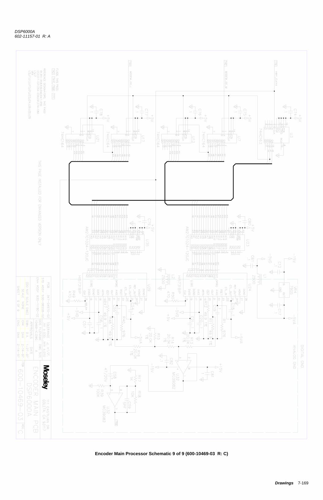
DSP6000A 602-11157-01 R: A
Drawings 7-169
Encoder Main Processor Schematic 9 of 9 (600-10469-03 R: C)

DSP6000A 602-11157-01 R: A
Drawings 7-170
This page is intentionally blank.
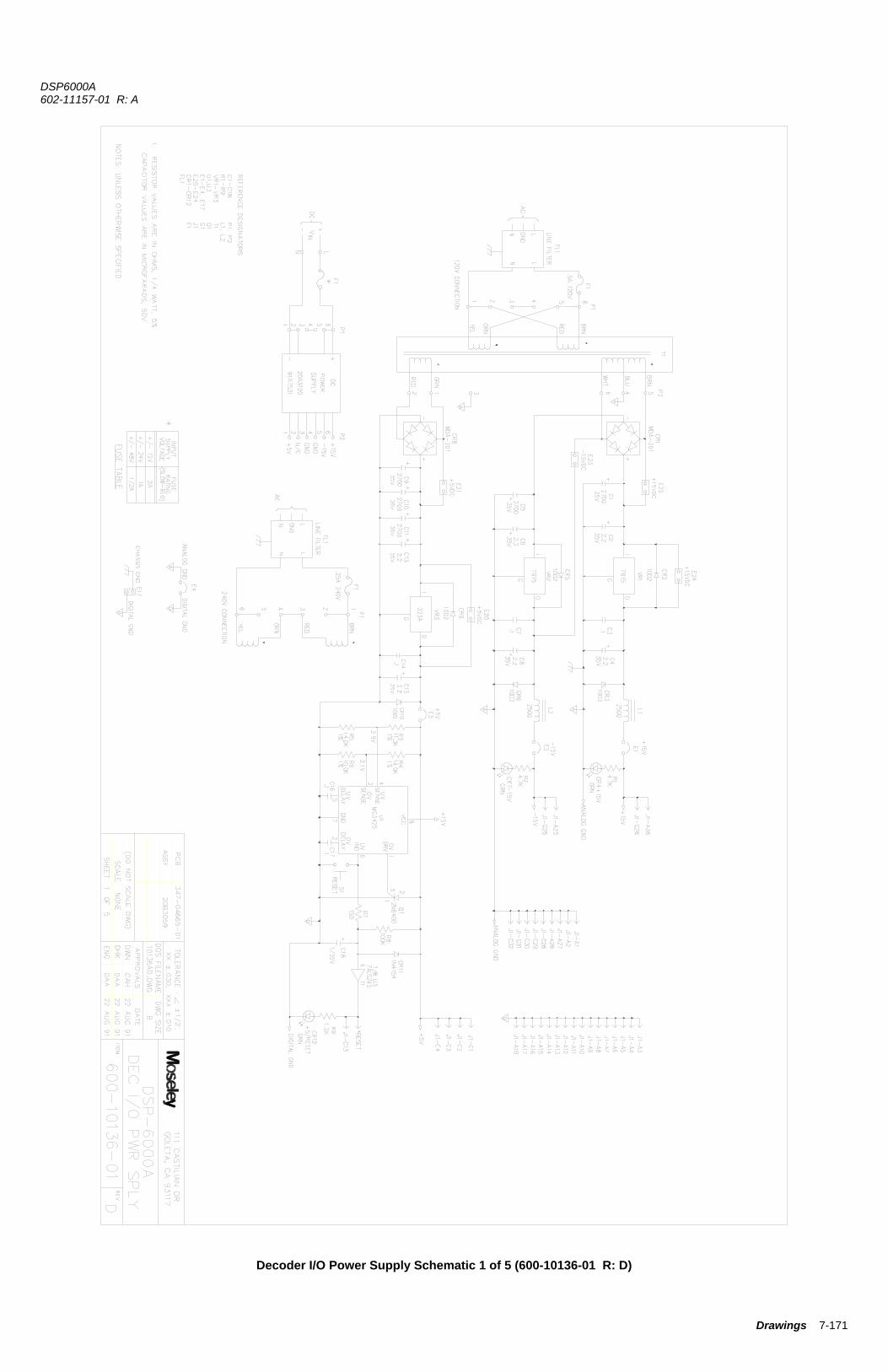
DSP6000A 602-11157-01 R: A
Drawings 7-171
Decoder I/O Power Supply Schematic 1 of 5 (600-10136-01 R: D)
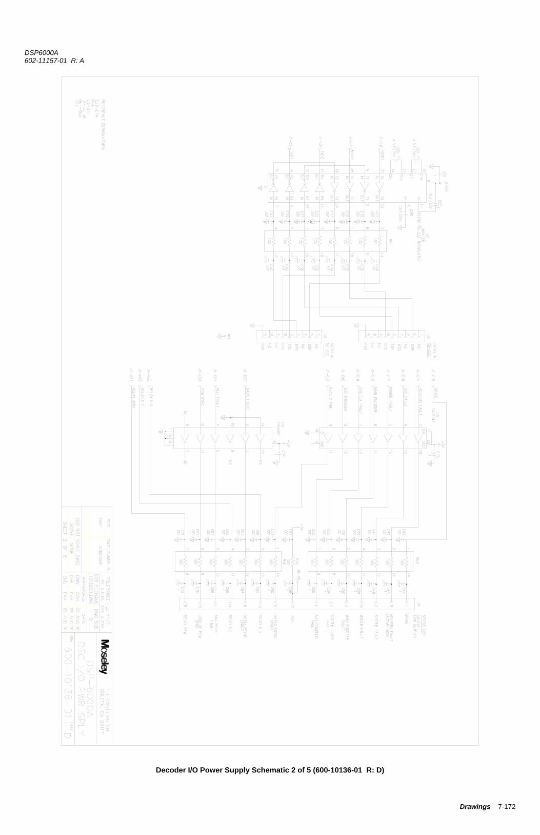
DSP6000A 602-11157-01 R: A
Drawings 7-172
Decoder I/O Power Supply Schematic 2 of 5 (600-10136-01 R: D)
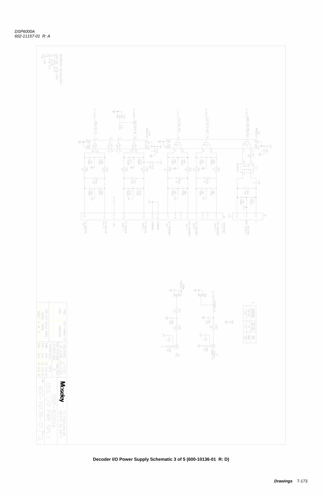
DSP6000A 602-11157-01 R: A
Drawings 7-173
Decoder I/O Power Supply Schematic 3 of 5 (600-10136-01 R: D)
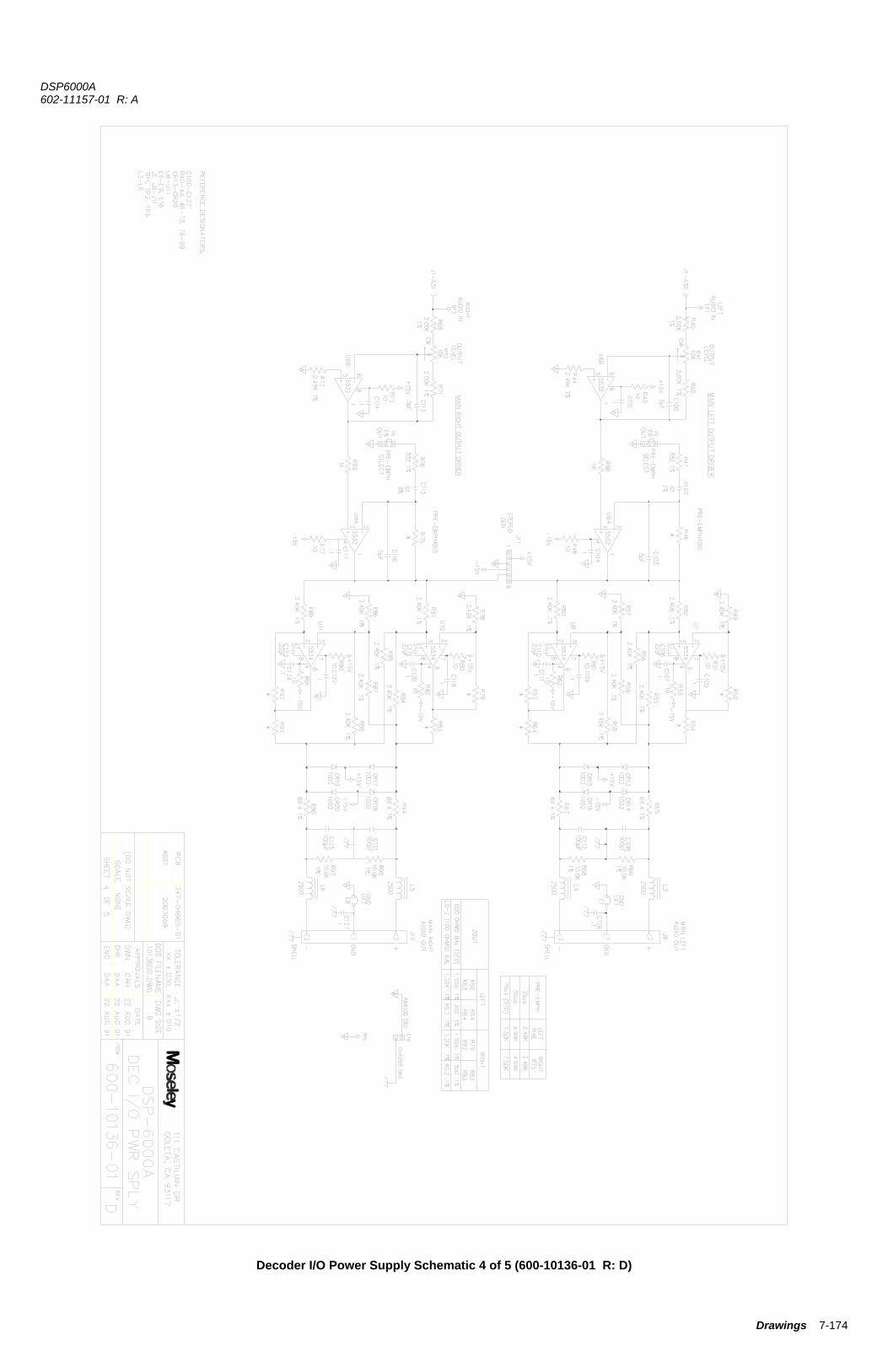
DSP6000A 602-11157-01 R: A
Drawings 7-174
Decoder I/O Power Supply Schematic 4 of 5 (600-10136-01 R: D)
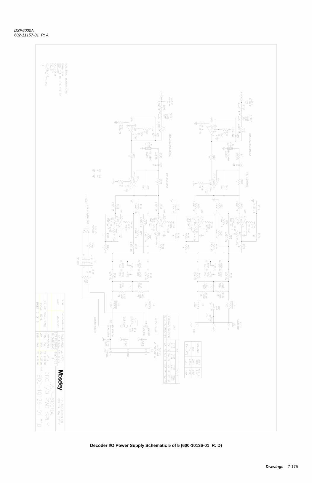
DSP6000A 602-11157-01 R: A
Drawings 7-175
Decoder I/O Power Supply Schematic 5 of 5 (600-10136-01 R: D)

DSP6000A 602-11157-01 R: A
Drawings 7-176
This page is intentionally blank.

DSP6000A 602-11157-01 R: A
Drawings 7-177
Decoder Main Processor Schematic 1 of 8 (91B7471 R: B)
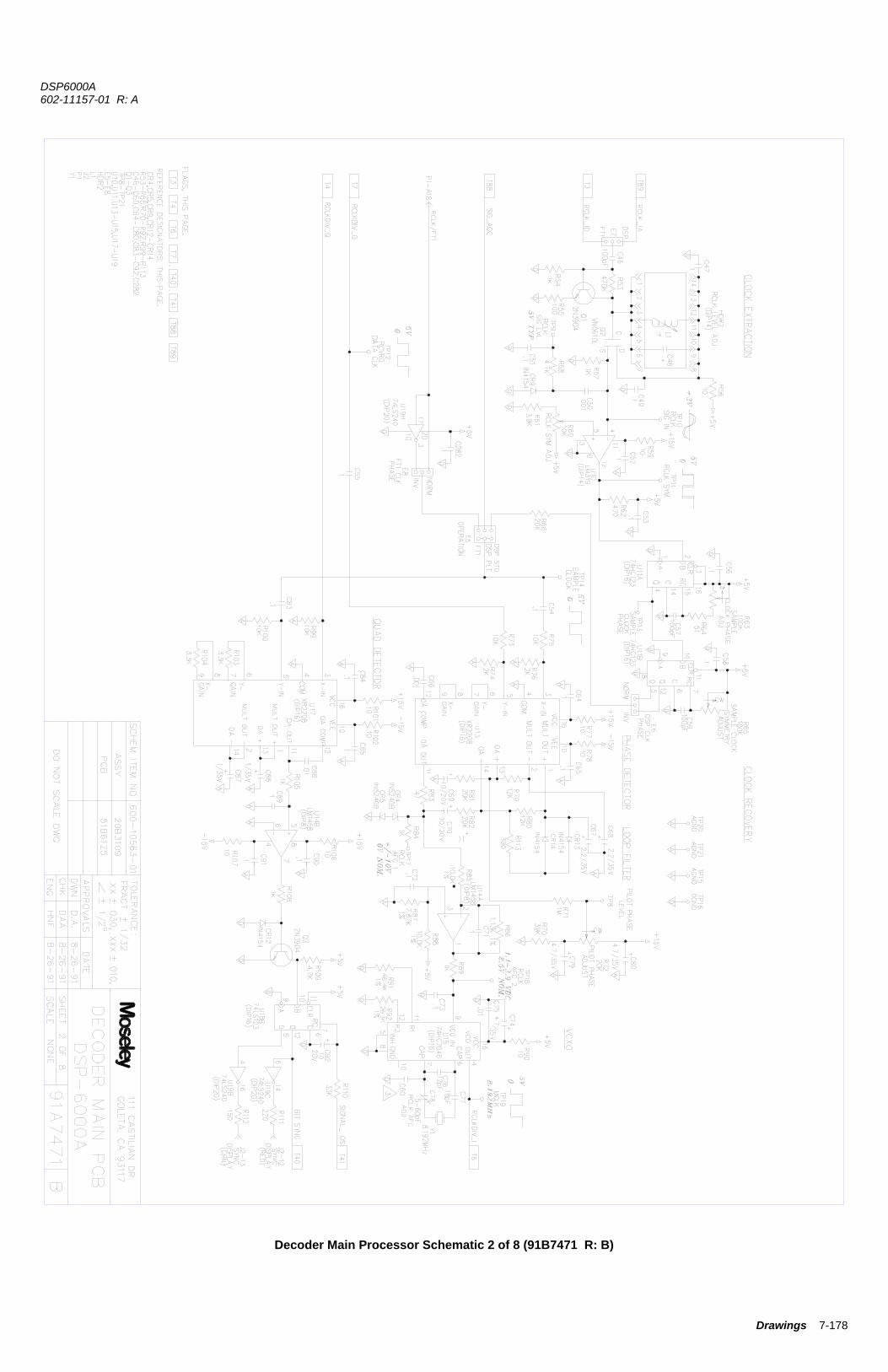
DSP6000A 602-11157-01 R: A
Drawings 7-178
Decoder Main Processor Schematic 2 of 8 (91B7471 R: B)
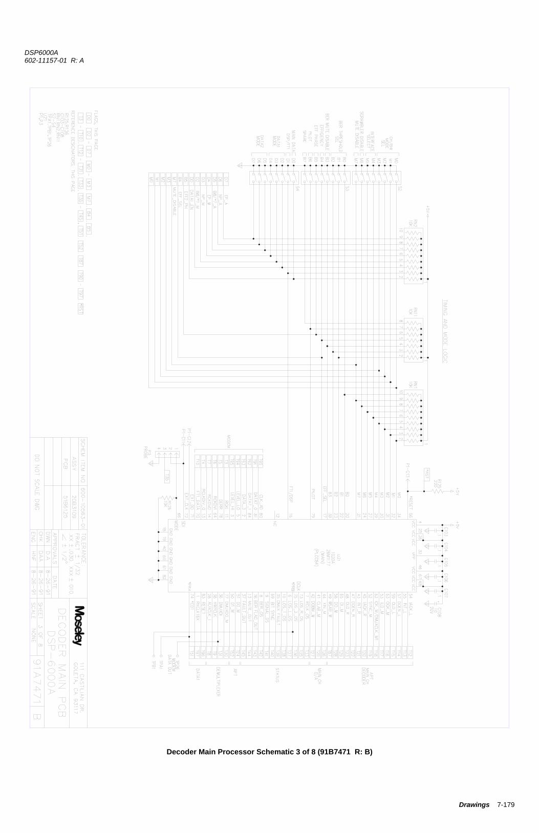
DSP6000A 602-11157-01 R: A
Drawings 7-179
Decoder Main Processor Schematic 3 of 8 (91B7471 R: B)
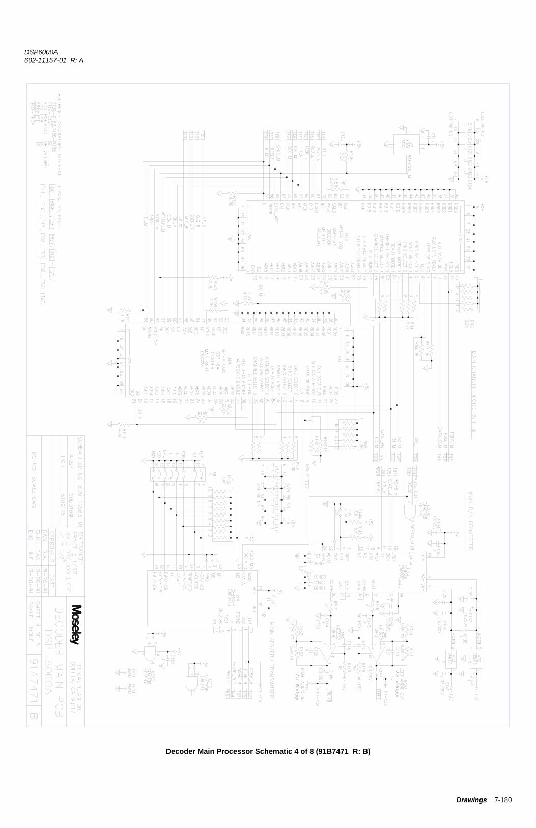
DSP6000A 602-11157-01 R: A
Drawings 7-180
Decoder Main Processor Schematic 4 of 8 (91B7471 R: B)
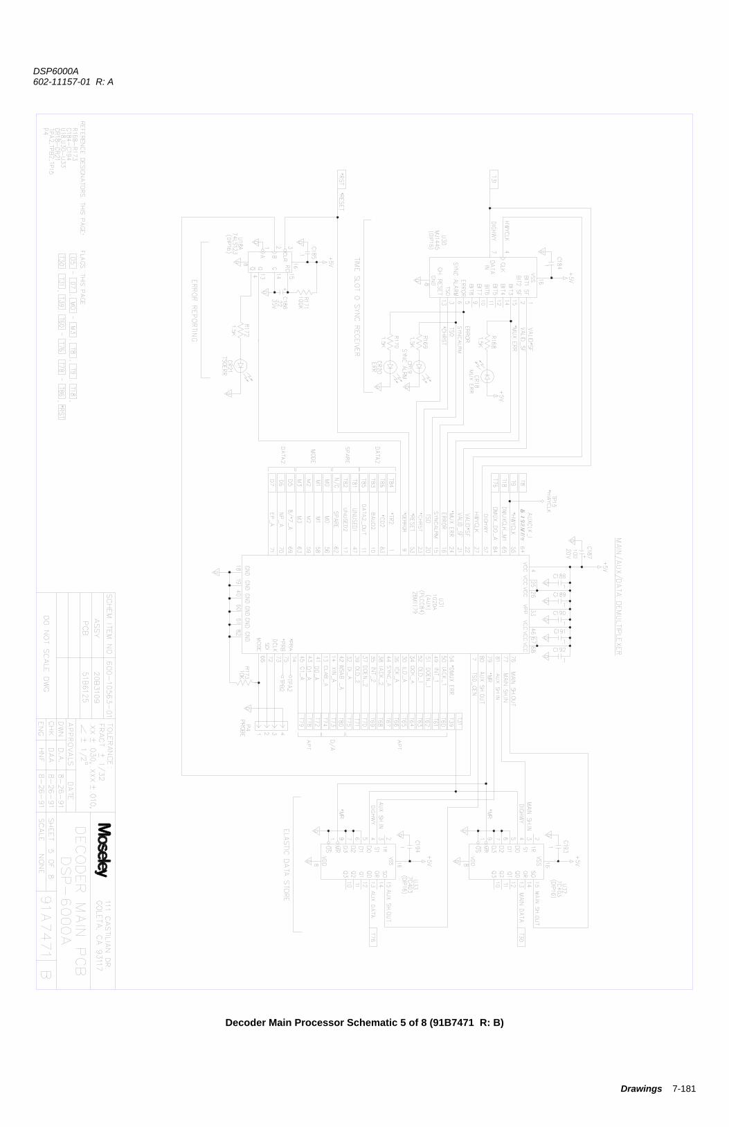
DSP6000A 602-11157-01 R: A
Drawings 7-181
Decoder Main Processor Schematic 5 of 8 (91B7471 R: B)
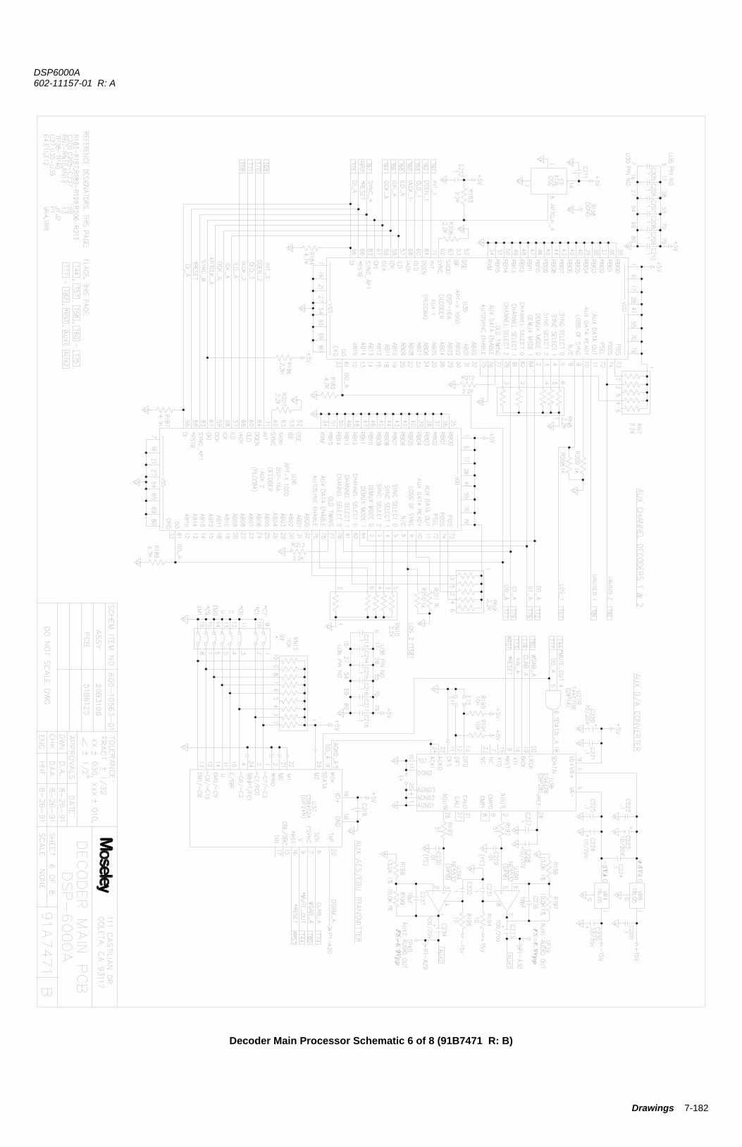
DSP6000A 602-11157-01 R: A
Drawings 7-182
Decoder Main Processor Schematic 6 of 8 (91B7471 R: B)
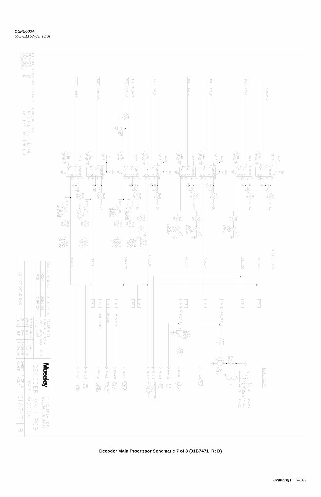
DSP6000A 602-11157-01 R: A
Drawings 7-183
Decoder Main Processor Schematic 7 of 8 (91B7471 R: B)
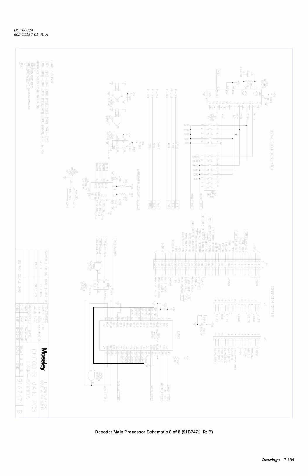
DSP6000A 602-11157-01 R: A
Drawings 7-184
Decoder Main Processor Schematic 8 of 8 (91B7471 R: B)
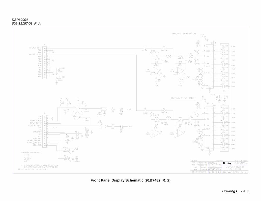
DSP6000A 602-11157-01 R: A
Drawings 7-185
Front Panel Display Schematic (91B7482 R: 2)
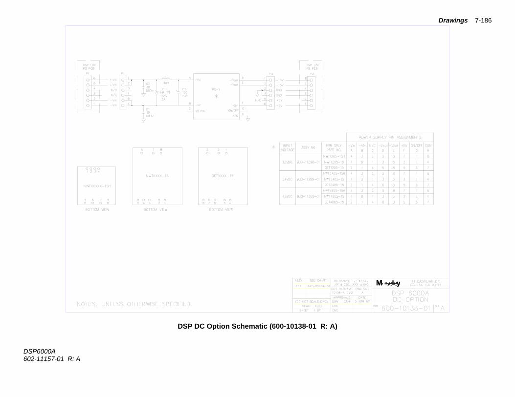
Drawings 7-186
DSP6000A 602-11157-01 R: A
DSP DC Option Schematic (600-10138-01 R: A)
Appendix A-187
DSP6000A 602-11157-AA1 R: A
Appendix
Section Contents Page
A.1 Path Evaluation Information A-2 A.2 Spectral Efficiency A-2 A.3 AES/EBU Digital Audio Data Format A-5 A.3.1 AES/EBU Standard A-5 A.3.2 DSP6000A AES/EBU Output A-7
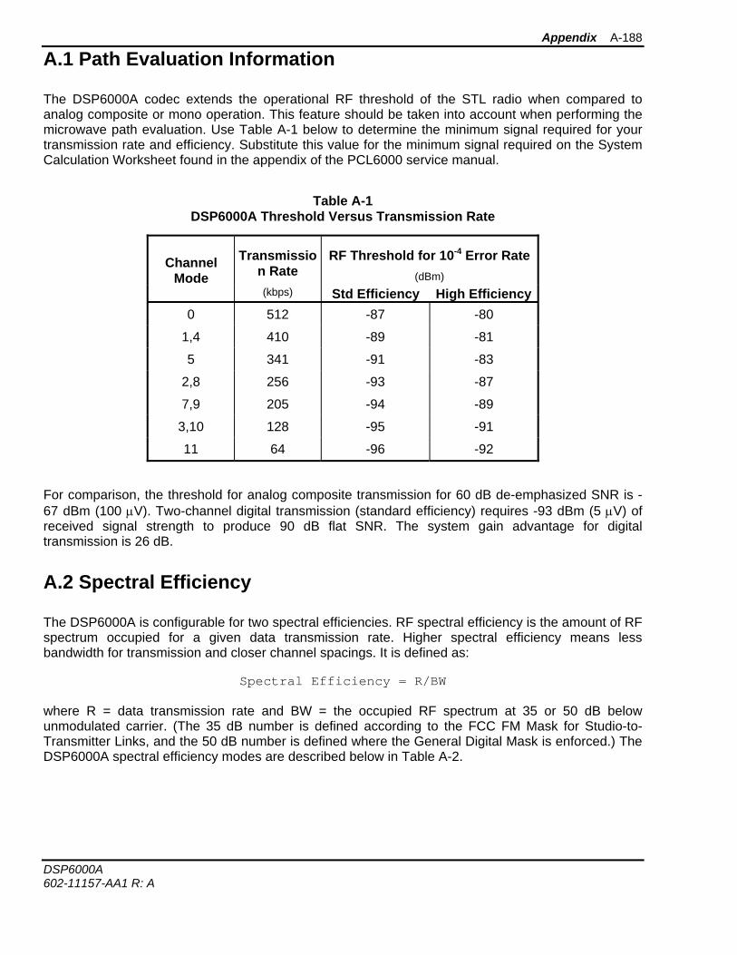
Appendix A-188
DSP6000A 602-11157-AA1 R: A
A.1 Path Evaluation Information
The DSP6000A codec extends the operational RF threshold of the STL radio when compared to analog composite or mono operation. This feature should be taken into account when performing the microwave path evaluation. Use Table A-1 below to determine the minimum signal required for your transmission rate and efficiency. Substitute this value for the minimum signal required on the System Calculation Worksheet found in the appendix of the PCL6000 service manual.
Table A-1 DSP6000A Threshold Versus Transmission Rate
Channel Mode
Transmission Rate
RF Threshold for 10-4 Error Rate (dBm)
(kbps) Std Efficiency High Efficiency 0 512 -87 -80
1,4 410 -89 -81
5 341 -91 -83
2,8 256 -93 -87
7,9 205 -94 -89
3,10 128 -95 -91
11 64 -96 -92
For comparison, the threshold for analog composite transmission for 60 dB de-emphasized SNR is -67 dBm (100 μV). Two-channel digital transmission (standard efficiency) requires -93 dBm (5 μV) of received signal strength to produce 90 dB flat SNR. The system gain advantage for digital transmission is 26 dB.
A.2 Spectral Efficiency
The DSP6000A is configurable for two spectral efficiencies. RF spectral efficiency is the amount of RF spectrum occupied for a given data transmission rate. Higher spectral efficiency means less bandwidth for transmission and closer channel spacings. It is defined as:
Spectral Efficiency = R/BW
where R = data transmission rate and BW = the occupied RF spectrum at 35 or 50 dB below unmodulated carrier. (The 35 dB number is defined according to the FCC FM Mask for Studio-to-Transmitter Links, and the 50 dB number is defined where the General Digital Mask is enforced.) The DSP6000A spectral efficiency modes are described below in Table A-2.
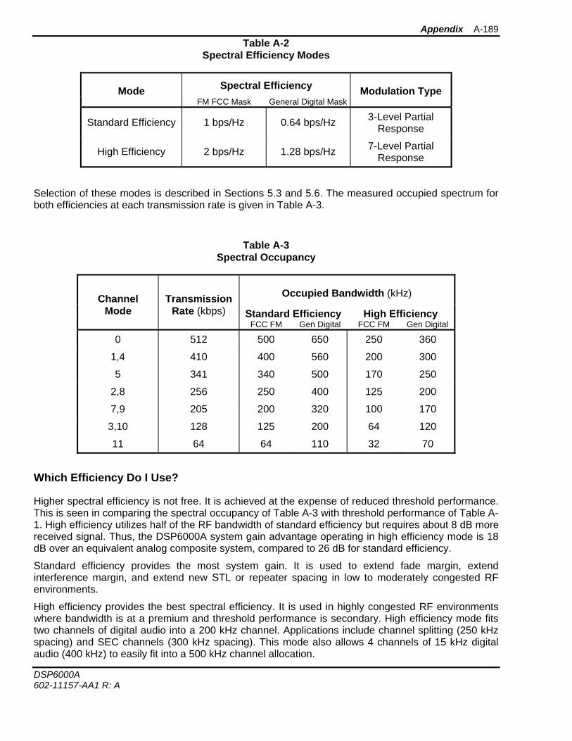
Appendix A-189
DSP6000A 602-11157-AA1 R: A
Table A-2 Spectral Efficiency Modes
Mode Spectral Efficiency Modulation Type FM FCC Mask General Digital Mask
Standard Efficiency 1 bps/Hz 0.64 bps/Hz 3-Level Partial Response
High Efficiency 2 bps/Hz 1.28 bps/Hz 7-Level Partial Response
Selection of these modes is described in Sections 5.3 and 5.6. The measured occupied spectrum for both efficiencies at each transmission rate is given in Table A-3.
Table A-3 Spectral Occupancy
Channel Transmission Occupied Bandwidth (kHz) Mode Rate (kbps) Standard Efficiency High Efficiency
FCC FM Gen Digital FCC FM Gen Digital
0 512 500 650 250 360
1,4 410 400 560 200 300
5 341 340 500 170 250
2,8 256 250 400 125 200
7,9 205 200 320 100 170
3,10 128 125 200 64 120
11 64 64 110 32 70
Which Efficiency Do I Use?
Higher spectral efficiency is not free. It is achieved at the expense of reduced threshold performance. This is seen in comparing the spectral occupancy of Table A-3 with threshold performance of Table A-1. High efficiency utilizes half of the RF bandwidth of standard efficiency but requires about 8 dB more received signal. Thus, the DSP6000A system gain advantage operating in high efficiency mode is 18 dB over an equivalent analog composite system, compared to 26 dB for standard efficiency.
Standard efficiency provides the most system gain. It is used to extend fade margin, extend interference margin, and extend new STL or repeater spacing in low to moderately congested RF environments.
High efficiency provides the best spectral efficiency. It is used in highly congested RF environments where bandwidth is at a premium and threshold performance is secondary. High efficiency mode fits two channels of digital audio into a 200 kHz channel. Applications include channel splitting (250 kHz spacing) and SEC channels (300 kHz spacing). This mode also allows 4 channels of 15 kHz digital audio (400 kHz) to easily fit into a 500 kHz channel allocation.
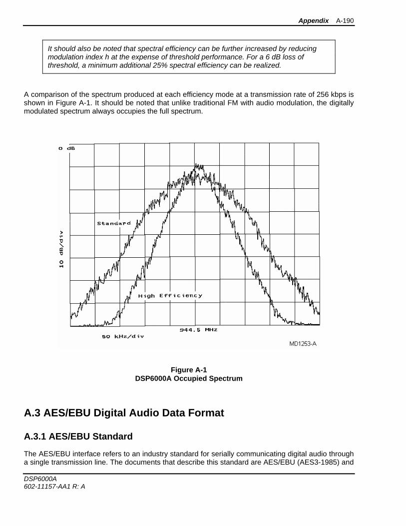
Appendix A-190
DSP6000A 602-11157-AA1 R: A
It should also be noted that spectral efficiency can be further increased by reducing modulation index h at the expense of threshold performance. For a 6 dB loss of threshold, a minimum additional 25% spectral efficiency can be realized.
A comparison of the spectrum produced at each efficiency mode at a transmission rate of 256 kbps is shown in Figure A-1. It should be noted that unlike traditional FM with audio modulation, the digitally modulated spectrum always occupies the full spectrum.
Figure A-1 DSP6000A Occupied Spectrum
A.3 AES/EBU Digital Audio Data Format
A.3.1 AES/EBU Standard
The AES/EBU interface refers to an industry standard for serially communicating digital audio through a single transmission line. The documents that describe this standard are AES/EBU (AES3-1985) and
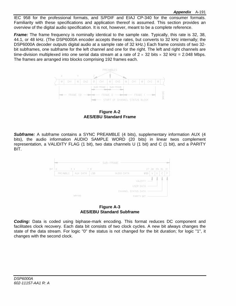
Appendix A-191
DSP6000A 602-11157-AA1 R: A
IEC 958 for the professional formats, and S/PDIF and EIAJ CP-340 for the consumer formats. Familiarity with these specifications and application thereof is assumed. This section provides an overview of the digital audio specification. It is not, however, meant to be a complete reference.
Frame: The frame frequency is nominally identical to the sample rate. Typically, this rate is 32, 38, 44.1, or 48 kHz. (The DSP6000A encoder accepts these rates, but converts to 32 kHz internally; the DSP6000A decoder outputs digital audio at a sample rate of 32 kHz.) Each frame consists of two 32-bit subframes, one subframe for the left channel and one for the right. The left and right channels are time-division multiplexed into one serial data stream at a rate of 2 × 32 bits × 32 kHz = 2.048 Mbps. The frames are arranged into blocks comprising 192 frames each.
Figure A-2 AES/EBU Standard Frame
Subframe: A subframe contains a SYNC PREAMBLE (4 bits), supplementary information AUX (4 bits), the audio information AUDIO SAMPLE WORD (20 bits) in linear twos complement representation, a VALIDITY FLAG (1 bit), two data channels U (1 bit) and C (1 bit), and a PARITY BIT.
Figure A-3 AES/EBU Standard Subframe
Coding: Data is coded using biphase-mark encoding. This format reduces DC component and facilitates clock recovery. Each data bit consists of two clock cycles. A new bit always changes the state of the data stream. For logic "0" the status is not changed for the bit duration; for logic "1", it changes with the second clock.
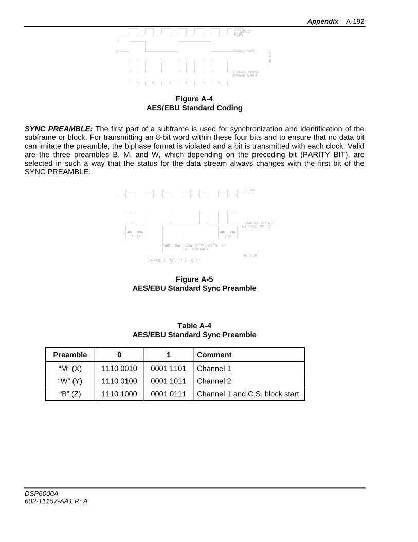
Appendix A-192
DSP6000A 602-11157-AA1 R: A
Figure A-4 AES/EBU Standard Coding
SYNC PREAMBLE: The first part of a subframe is used for synchronization and identification of the subframe or block. For transmitting an 8-bit word within these four bits and to ensure that no data bit can imitate the preamble, the biphase format is violated and a bit is transmitted with each clock. Valid are the three preambles B, M, and W, which depending on the preceding bit (PARITY BIT), are selected in such a way that the status for the data stream always changes with the first bit of the SYNC PREAMBLE.
Figure A-5 AES/EBU Standard Sync Preamble
Table A-4 AES/EBU Standard Sync Preamble
Preamble 0 1 Comment
“M” (X) 1110 0010 0001 1101 Channel 1
“W” (Y) 1110 0100 0001 1011 Channel 2
“B” (Z) 1110 1000 0001 0111 Channel 1 and C.S. block start
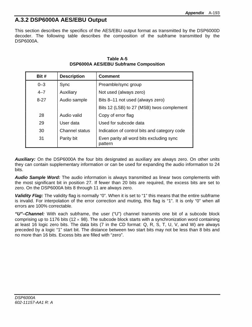
Appendix A-193
DSP6000A 602-11157-AA1 R: A
A.3.2 DSP6000A AES/EBU Output
This section describes the specifics of the AES/EBU output format as transmitted by the DSP6000D decoder. The following table describes the composition of the subframe transmitted by the DSP6000A.
Table A-5 DSP6000A AES/EBU Subframe Composition
Bit # Description Comment
0–3 Sync Preamble/sync group
4–7 Auxiliary Not used (always zero)
8-27 Audio sample Bits 8–11 not used (always zero)
Bits 12 (LSB) to 27 (MSB) twos complement
28 Audio valid Copy of error flag
29 User data Used for subcode data
30 Channel status Indication of control bits and category code
31 Parity bit Even parity all word bits excluding sync pattern
Auxiliary: On the DSP6000A the four bits designated as auxiliary are always zero. On other units they can contain supplementary information or can be used for expanding the audio information to 24 bits.
Audio Sample Word: The audio information is always transmitted as linear twos complements with the most significant bit in position 27. If fewer than 20 bits are required, the excess bits are set to zero. On the DSP6000A bits 8 through 11 are always zero.
Validity Flag: The validity flag is normally “0”. When it is set to “1” this means that the entire subframe is invalid. For interpolation of the error correction and muting, this flag is “1”. It is only “0” when all errors are 100% correctable.
“U”–Channel: With each subframe, the user (“U”) channel transmits one bit of a subcode block comprising up to 1176 bits (12 × 98). The subcode block starts with a synchronization word containing at least 16 logic zero bits. The data bits (7 in the CD format: Q, R, S, T, U, V, and W) are always preceded by a logic “1” start bit. The distance between two start bits may not be less than 8 bits and no more than 16 bits. Excess bits are filled with “zero”.
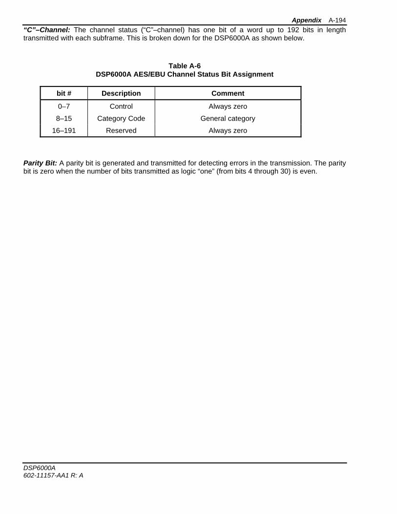
Appendix A-194
DSP6000A 602-11157-AA1 R: A
“C”–Channel: The channel status (“C”–channel) has one bit of a word up to 192 bits in length transmitted with each subframe. This is broken down for the DSP6000A as shown below.
Table A-6 DSP6000A AES/EBU Channel Status Bit Assignment
bit # Description Comment
0–7 Control Always zero
8–15 Category Code General category
16–191 Reserved Always zero
Parity Bit: A parity bit is generated and transmitted for detecting errors in the transmission. The parity bit is zero when the number of bits transmitted as logic “one” (from bits 4 through 30) is even.
DSP6000A 602-11157-AA1 R: A
Table of Contents
Section Contents Page
Table of Contents i List of Figures v List of Tables vii Glossary x About this Manual xii 1 System Characteristics 1.1 Introduction 1-2 1.2 System Features 1-3 1.3 DSP6000A System 1-4 1.3.1 DSP6000A System Specifications 1-4 1.3.2 DSP6000E Encoder Specifications 1-5 1.3.3 DSP6000D Decoder Specifications 1-6 1.4 System Description 1-7 1.4.1 DSP6000E Encoder Description 1-7 1.4.2 DSP6000D Decoder Description 1-11 2 Installation 2.1 Unpacking 2-2 2.2 Power 2-2 2.2.1 AC Line Voltage Selection 2-2 2.2.2 DC Option Fuses 2-4 2.3 Pre-Installation Checkout 2-5 2.3.1 Checkout of Encoder/Decoder Only 2-5 2.3.2 Checkout of System — Encoder/STL/Decoder 2-7 2.4 Rack Installation 2-9 2.5 STL Installation 2-10 2.5.1 Encoder 2-10 2.5.2 Decoder 2-12 2.5.3 Air-Chain Processing 2-14 2.5.4 Repeater 2-16 2.6 Fractional T1 (FT1) Installation 2-18 2.7 Data Communications 2-22 2.7.1 Data Rate and Format Selection 2-22 2.7.2 Remote Control Communication 2-23 2.7.2.1 Subcarrier Communications 2-23 2.7.2.2 FSK Communications 2-23
Table of Contents 196
DSP6000A 602-11157-TC1 R: A
Section Contents Page
2.7.2.3 RS-232 Communications 2-24 2.8 Retrofit STL Installation 2-31 2.8.1 PCL6010 Transmitter 2-31 2.8.2 PCL6020/6030/6060 Receiver 2-32 2.8.3 PCL606 Transmitter, Mono 2-36 2.8.4 PCL606 Receiver, Mono 2-38 2.8.5 PCL606/C Transmitter, Composite 2-40 2.8.6 PCL606/C Receiver, Composite 2-41 2.8.7 PCL505 Transmitter, Composite 2-43 2.8.8 PCL505 Receiver, Composite 2-44 2.8.9 Other Radios 2-45 2.8.10 Retrofit Repeater Installation with STL 2-46 3 Operation 3.1 Encoder Front Panel 3-2 3.2 Encoder Back Panel 3-3 3.3 Encoder Pin Assignments 3-4 3.4 Decoder Front Panel 3-6 3.5 Decoder Back Panel 3-7 3.6 Decoder Pin Assignments 3-8 4 Customer Service Information 4.1 Introduction 4-2 4.2 Technical Consultation 4-2 4.3 Factory Service 4-3 4.4 Field Repair 4-4 5 Configuration 5.1 Introduction 5-2 5.2 Encoder Channel Configuration 5-3 5.3 Encoder Alignment 5-5 5.4 Encoder Interface Configuration 5-9 5.4.1 Interface Mode 0 — PROGRAM, FT1 SEND 5-10 5.4.2 Interface Mode 1 — REPEATER 5-11 5.4.3 Interface Mode 2 — AES/EBU, FT1 SEND 5-12 5.4.4 Interface Mode 3 — PCM 5-13 5.4.5 Interface Mode 4 — PROGRAM, FT1 RECEIVE 5-14 5.4.6 Interface Mode 5 — AES/EBU, FT1 RECEIVE 5-15 5.5 Decoder Channel Configuration 5-16 5.6 Decoder Alignment 5-18 5.6.1 Decoder Alignment — Standard Efficiency 5-21
Table of Contents 197
DSP6000A 602-11157-TC1 R: A
Section Contents Page
5.6.2 Decoder Alignment — High Efficiency with Pilot 5-23 5.6.3 Decoder Alignment — Standard Efficiency with Pilot 5-25 5.6.4 Decoder Alignment — FT1 5-27 5.7 Decoder Interface Configuration 5-27 5.7.1 Interface Mode 0 — PROGRAM 5-28 5.7.2 Interface Mode 1 — REPEATER 5-29 5.7.3 Interface Mode 2 — AES/EBU 5-30 5.7.4 Interface Mode 3 — PCM 5-31 5.7.5 STL Interface Mode 5-32 5.7.6 FT1 Interface Mode 5-32 5.8 Changing Transmission Efficiency 5-33 5.9 Data Channel Configuration 5-33 5.9.1 DATA 1 (RS-232) 5-35 5.9.1 DATA 2 (RS-232) 5-37 5.10 BER Threshold Selection 5-38 5.11 Automatic Audio Mute 5-39 5.12 Scrambler Disable 5-39 5.13 Configuration Programming Summary Tables 5-40 6 Troubleshooting and Testing 6.1 Audio Measurements 6-2 6.1.1 Signal-to-Noise Ratio 6-2 6.1.2 Distortion/SINAD 6-4 6.2 Troubleshooting 6-4 6.2.1 Encoder STATUS Output 6-5 6.2.2 Decoder STATUS Output 6-7 6.3 Board Alignment Information 6-9 6.3.1 Encoder 6-9 6.3.1.1 Encoder I/O Power Supply Board 6-9 6.3.1.2 Encoder Main Processor Board 6-12 6.3.1.3 Encoder Display Board 6-15 6.3.2 Decoder 6-16 6.3.2.1 Decoder I/O Power Supply Board 6-16 6.3.2.2 Decoder Main Processor 6-19 6.3.2.3 Decoder Display Board 6-24 6.4 Test Equipment 6-26 6.5 Test Fixture Diagrams 6-27 7 Schematic and Assembly Drawings Appendix A.1 Path Evaluation Information A-2 A.2 Spectral Efficiency A-2 A.3 AES/EBU Digital Audio Data Format A-5 A.3.1 AES/EBU Standard A-5 A.3.2 DSP6000A AES/EBU Output A-7
Table of Contents 198
DSP6000A 602-11157-TC1 R: A
Section Contents Page
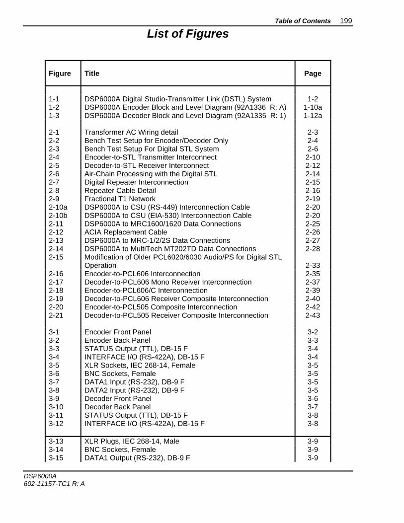
Table of Contents 199
DSP6000A 602-11157-TC1 R: A
List of Figures
Figure Title Page
1-1 DSP6000A Digital Studio-Transmitter Link (DSTL) System 1-2 1-2 DSP6000A Encoder Block and Level Diagram (92A1336 R: A) 1-10a 1-3 DSP6000A Decoder Block and Level Diagram (92A1335 R: 1) 1-12a 2-1 Transformer AC Wiring detail 2-3 2-2 Bench Test Setup for Encoder/Decoder Only 2-4 2-3 Bench Test Setup For Digital STL System 2-6 2-4 Encoder-to-STL Transmitter Interconnect 2-10 2-5 Decoder-to-STL Receiver Interconnect 2-12 2-6 Air-Chain Processing with the Digital STL 2-14 2-7 Digital Repeater Interconnection 2-15 2-8 Repeater Cable Detail 2-16 2-9 Fractional T1 Network 2-19 2-10a DSP6000A to CSU (RS-449) Interconnection Cable 2-20 2-10b DSP6000A to CSU (EIA-530) Interconnection Cable 2-20 2-11 DSP6000A to MRC1600/1620 Data Connections 2-25 2-12 ACIA Replacement Cable 2-26 2-13 DSP6000A to MRC-1/2/2S Data Connections 2-27 2-14 DSP6000A to MultiTech MT202TD Data Connections 2-28 2-15 Modification of Older PCL6020/6030 Audio/PS for Digital STL
Operation
2-33 2-16 Encoder-to-PCL606 Interconnection 2-35 2-17 Decoder-to-PCL606 Mono Receiver Interconnection 2-37 2-18 Encoder-to-PCL606/C Interconnection 2-39 2-19 Decoder-to-PCL606 Receiver Composite Interconnection 2-40 2-20 Encoder-to-PCL505 Composite Interconnection 2-42 2-21 Decoder-to-PCL505 Receiver Composite Interconnection 2-43 3-1 Encoder Front Panel 3-2 3-2 Encoder Back Panel 3-3 3-3 STATUS Output (TTL), DB-15 F 3-4 3-4 INTERFACE I/O (RS-422A), DB-15 F 3-4 3-5 XLR Sockets, IEC 268-14, Female 3-5 3-6 BNC Sockets, Female 3-5 3-7 DATA1 Input (RS-232), DB-9 F 3-5 3-8 DATA2 Input (RS-232), DB-9 F 3-5 3-9 Decoder Front Panel 3-6 3-10 Decoder Back Panel 3-7 3-11 STATUS Output (TTL), DB-15 F 3-8 3-12 INTERFACE I/O (RS-422A), DB-15 F 3-8 3-13 XLR Plugs, IEC 268-14, Male 3-9 3-14 BNC Sockets, Female 3-9 3-15 DATA1 Output (RS-232), DB-9 F 3-9
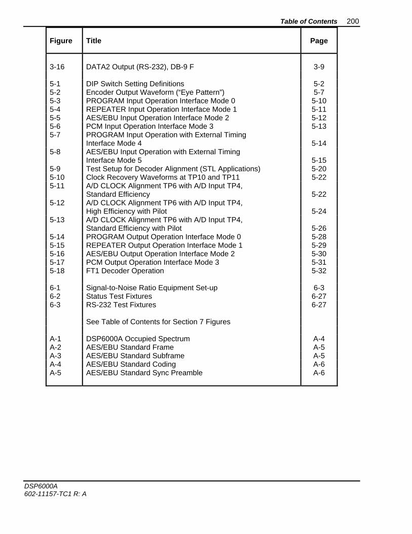
Table of Contents 200
DSP6000A 602-11157-TC1 R: A
Figure Title Page
3-16 DATA2 Output (RS-232), DB-9 F 3-9 5-1 DIP Switch Setting Definitions 5-2 5-2 Encoder Output Waveform (“Eye Pattern”) 5-7 5-3 PROGRAM Input Operation Interface Mode 0 5-10 5-4 REPEATER Input Operation Interface Mode 1 5-11 5-5 AES/EBU Input Operation Interface Mode 2 5-12 5-6 PCM Input Operation Interface Mode 3 5-13 5-7 PROGRAM Input Operation with External Timing
Interface Mode 4
5-14 5-8 AES/EBU Input Operation with External Timing
Interface Mode 5
5-15 5-9 Test Setup for Decoder Alignment (STL Applications) 5-20 5-10 Clock Recovery Waveforms at TP10 and TP11 5-22 5-11 A/D CLOCK Alignment TP6 with A/D Input TP4,
Standard Efficiency
5-22 5-12 A/D CLOCK Alignment TP6 with A/D Input TP4,
High Efficiency with Pilot
5-24 5-13 A/D CLOCK Alignment TP6 with A/D Input TP4,
Standard Efficiency with Pilot
5-26 5-14 PROGRAM Output Operation Interface Mode 0 5-28 5-15 REPEATER Output Operation Interface Mode 1 5-29 5-16 AES/EBU Output Operation Interface Mode 2 5-30 5-17 PCM Output Operation Interface Mode 3 5-31 5-18 FT1 Decoder Operation 5-32 6-1 Signal-to-Noise Ratio Equipment Set-up 6-3 6-2 Status Test Fixtures 6-27 6-3 RS-232 Test Fixtures 6-27 See Table of Contents for Section 7 Figures A-1 DSP6000A Occupied Spectrum A-4 A-2 AES/EBU Standard Frame A-5 A-3 AES/EBU Standard Subframe A-5 A-4 AES/EBU Standard Coding A-6 A-5 AES/EBU Standard Sync Preamble A-6
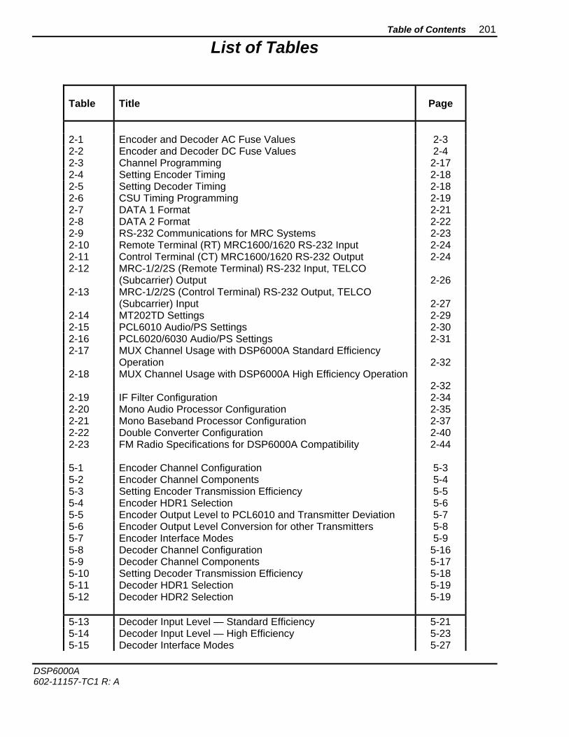
Table of Contents 201
DSP6000A 602-11157-TC1 R: A
List of Tables
Table Title Page
2-1 Encoder and Decoder AC Fuse Values 2-3 2-2 Encoder and Decoder DC Fuse Values 2-4 2-3 Channel Programming 2-17 2-4 Setting Encoder Timing 2-18 2-5 Setting Decoder Timing 2-18 2-6 CSU Timing Programming 2-19 2-7 DATA 1 Format 2-21 2-8 DATA 2 Format 2-22 2-9 RS-232 Communications for MRC Systems 2-23 2-10 Remote Terminal (RT) MRC1600/1620 RS-232 Input 2-24 2-11 Control Terminal (CT) MRC1600/1620 RS-232 Output 2-24 2-12 MRC-1/2/2S (Remote Terminal) RS-232 Input, TELCO
(Subcarrier) Output
2-26 2-13 MRC-1/2/2S (Control Terminal) RS-232 Output, TELCO
(Subcarrier) Input
2-27 2-14 MT202TD Settings 2-29 2-15 PCL6010 Audio/PS Settings 2-30 2-16 PCL6020/6030 Audio/PS Settings 2-31 2-17 MUX Channel Usage with DSP6000A Standard Efficiency
Operation
2-32 2-18 MUX Channel Usage with DSP6000A High Efficiency Operation
2-32 2-19 IF Filter Configuration 2-34 2-20 Mono Audio Processor Configuration 2-35 2-21 Mono Baseband Processor Configuration 2-37 2-22 Double Converter Configuration 2-40 2-23 FM Radio Specifications for DSP6000A Compatibility 2-44 5-1 Encoder Channel Configuration 5-3 5-2 Encoder Channel Components 5-4 5-3 Setting Encoder Transmission Efficiency 5-5 5-4 Encoder HDR1 Selection 5-6 5-5 Encoder Output Level to PCL6010 and Transmitter Deviation 5-7 5-6 Encoder Output Level Conversion for other Transmitters 5-8 5-7 Encoder Interface Modes 5-9 5-8 Decoder Channel Configuration 5-16 5-9 Decoder Channel Components 5-17 5-10 Setting Decoder Transmission Efficiency 5-18 5-11 Decoder HDR1 Selection 5-19 5-12 Decoder HDR2 Selection 5-19 5-13 Decoder Input Level — Standard Efficiency 5-21 5-14 Decoder Input Level — High Efficiency 5-23 5-15 Decoder Interface Modes 5-27
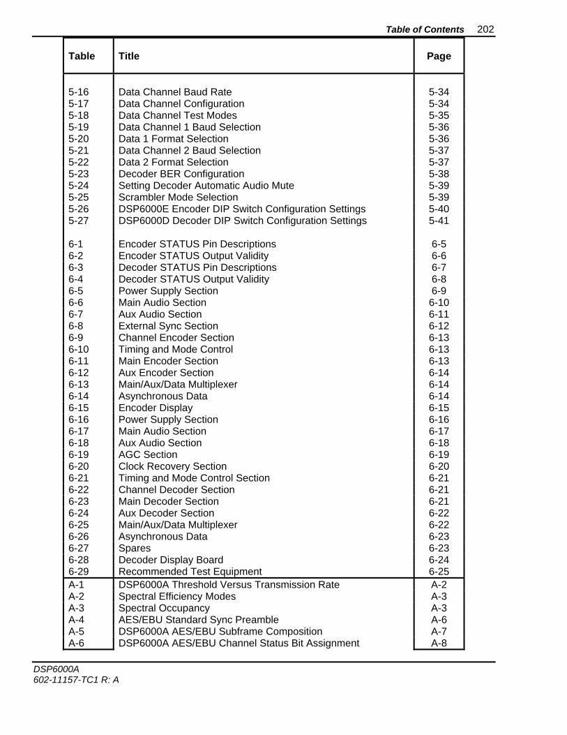
Table of Contents 202
DSP6000A 602-11157-TC1 R: A
Table Title Page
5-16 Data Channel Baud Rate 5-34 5-17 Data Channel Configuration 5-34 5-18 Data Channel Test Modes 5-35 5-19 Data Channel 1 Baud Selection 5-36 5-20 Data 1 Format Selection 5-36 5-21 Data Channel 2 Baud Selection 5-37 5-22 Data 2 Format Selection 5-37 5-23 Decoder BER Configuration 5-38 5-24 Setting Decoder Automatic Audio Mute 5-39 5-25 Scrambler Mode Selection 5-39 5-26 DSP6000E Encoder DIP Switch Configuration Settings 5-40 5-27 DSP6000D Decoder DIP Switch Configuration Settings 5-41 6-1 Encoder STATUS Pin Descriptions 6-5 6-2 Encoder STATUS Output Validity 6-6 6-3 Decoder STATUS Pin Descriptions 6-7 6-4 Decoder STATUS Output Validity 6-8 6-5 Power Supply Section 6-9 6-6 Main Audio Section 6-10 6-7 Aux Audio Section 6-11 6-8 External Sync Section 6-12 6-9 Channel Encoder Section 6-13 6-10 Timing and Mode Control 6-13 6-11 Main Encoder Section 6-13 6-12 Aux Encoder Section 6-14 6-13 Main/Aux/Data Multiplexer 6-14 6-14 Asynchronous Data 6-14 6-15 Encoder Display 6-15 6-16 Power Supply Section 6-16 6-17 Main Audio Section 6-17 6-18 Aux Audio Section 6-18 6-19 AGC Section 6-19 6-20 Clock Recovery Section 6-20 6-21 Timing and Mode Control Section 6-21 6-22 Channel Decoder Section 6-21 6-23 Main Decoder Section 6-21 6-24 Aux Decoder Section 6-22 6-25 Main/Aux/Data Multiplexer 6-22 6-26 Asynchronous Data 6-23 6-27 Spares 6-23 6-28 Decoder Display Board 6-24 6-29 Recommended Test Equipment 6-25 A-1 DSP6000A Threshold Versus Transmission Rate A-2 A-2 Spectral Efficiency Modes A-3 A-3 Spectral Occupancy A-3 A-4 AES/EBU Standard Sync Preamble A-6 A-5 DSP6000A AES/EBU Subframe Composition A-7 A-6 DSP6000A AES/EBU Channel Status Bit Assignment A-8
Table of Contents 203
DSP6000A 602-11157-TC1 R: A
Table Title Page
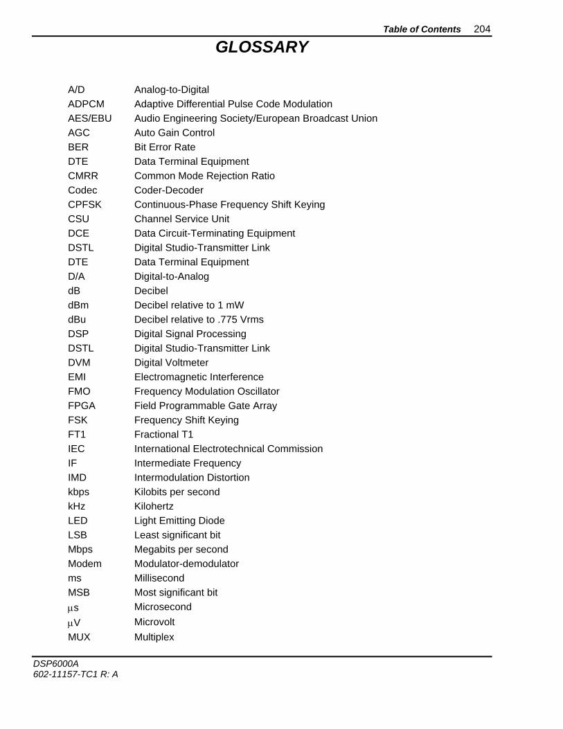
Table of Contents 204
DSP6000A 602-11157-TC1 R: A
GLOSSARY
A/D Analog-to-Digital ADPCM Adaptive Differential Pulse Code Modulation AES/EBU Audio Engineering Society/European Broadcast Union AGC Auto Gain Control BER Bit Error Rate DTE Data Terminal Equipment CMRR Common Mode Rejection Ratio Codec Coder-Decoder CPFSK Continuous-Phase Frequency Shift Keying CSU Channel Service Unit DCE Data Circuit-Terminating Equipment DSTL Digital Studio-Transmitter Link DTE Data Terminal Equipment D/A Digital-to-Analog dB Decibel dBm Decibel relative to 1 mW dBu Decibel relative to .775 Vrms DSP Digital Signal Processing DSTL Digital Studio-Transmitter Link DVM Digital Voltmeter EMI Electromagnetic Interference FMO Frequency Modulation Oscillator FPGA Field Programmable Gate Array FSK Frequency Shift Keying FT1 Fractional T1 IEC International Electrotechnical Commission IF Intermediate Frequency IMD Intermodulation Distortion kbps Kilobits per second kHz Kilohertz LED Light Emitting Diode LSB Least significant bit Mbps Megabits per second Modem Modulator-demodulator ms Millisecond MSB Most significant bit μs Microsecond μV Microvolt MUX Multiplex
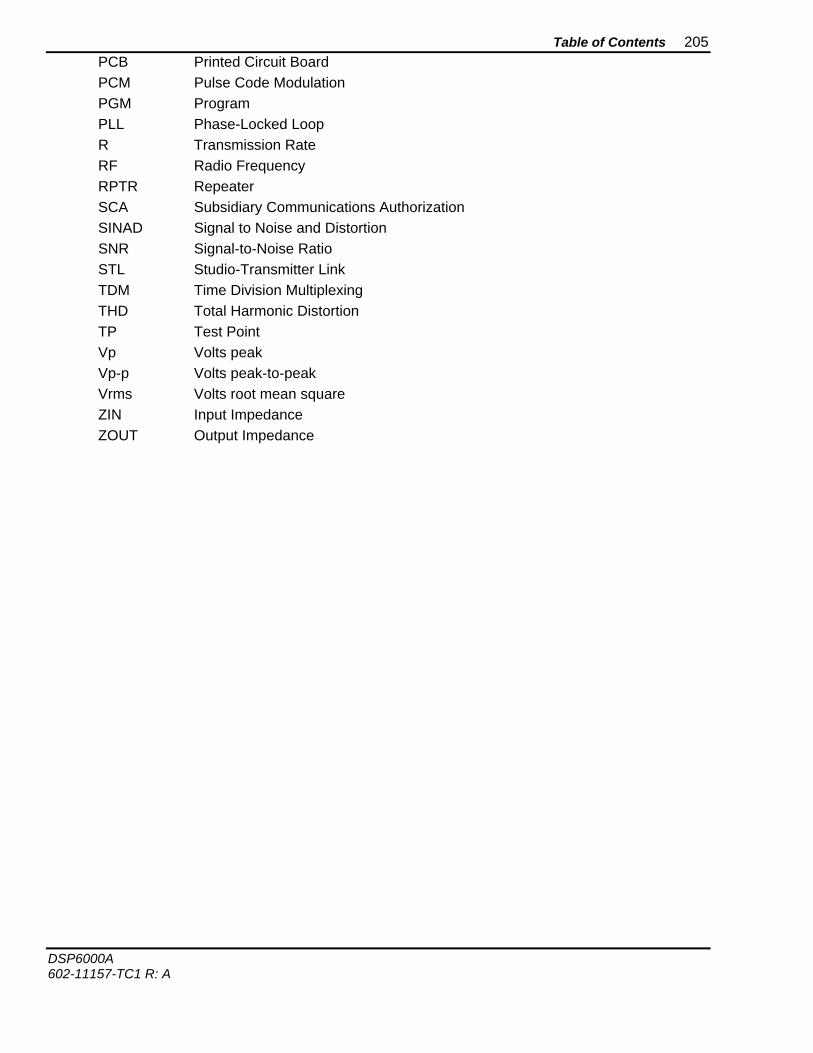
Table of Contents 205
DSP6000A 602-11157-TC1 R: A
PCB Printed Circuit Board PCM Pulse Code Modulation PGM Program PLL Phase-Locked Loop R Transmission Rate RF Radio Frequency RPTR Repeater SCA Subsidiary Communications Authorization SINAD Signal to Noise and Distortion SNR Signal-to-Noise Ratio STL Studio-Transmitter Link TDM Time Division Multiplexing THD Total Harmonic Distortion TP Test Point Vp Volts peak Vp-p Volts peak-to-peak Vrms Volts root mean square ZIN Input Impedance ZOUT Output Impedance
Table of Contents 206
DSP6000A 602-11157-TC1 R: A
About This Manual
This manual is a comprehensive operation guide to the DSP6000A Digital Studio-Transmitter Link with information for new installations, retrofit installations, configuration, alignment, and general troubleshooting in the field.
If you are unfamiliar with the basic use of the DSP6000A, read Sections 1 through 3 before installing any equipment. Sections 4 through the appendix will aid those in need of more detailed information on the operation of this system.
Section 1, System Characteristics, is a brief overview of the DSP6000A. It includes encoder and decoder specifications, features, and system descriptions.
Section 2, Installation, covers unpacking, installation, and checkout procedures. It also describes retrofit modifications for STL’s and remote controls.
Section 3, Operation, discusses the controls, adjustments, and I/O operations for the DSP6000A system that the user will encounter in normal operation and initial setup.
Section 4, Customer Service, tells how to get technical assistance or return equipment for factory service, and provides some field repair basics.
Section 5, Configuration, presents programming information for the various configurations of the system. Alignment information is also included.
Section 6, Troubleshooting and Testing, covers audio performance checks, troubleshooting aids, and user adjustments that are used to service and maintain the DSP6000A. This section also includes recommended test equipment and test fixtures.
Section 7, Schematic and Assembly Drawings, contains system schematics and board diagrams to aid in troubleshooting and field repair. The Appendix contains addendum information to the 950 MHz Microwave path evaluation, spectral occupancy information, and AES/EBU digital audio data format overview.


![FM Microwave Radio Link - Elber radio TV broadcast …UserManuals~NBFM_[EN].pdfFM Microwave Radio Link Transmitter T_NBFM-01 ... microwave radio link. It is able to transfer, over](https://img.pdfslide.us/doc/110x75/5ab9bcd47f8b9aa6018e34cf/fm-microwave-radio-link-elber-radio-tv-broadcast-usermanualsnbfmenpdffm.jpg)


![[PSS EML0610A-(en)] 144LD Intelligent Buoyancy Transmitter ... · 144LD Intelligent Buoyancy Transmitter with Torque Tube ... FFspecification Rev. 1.4, Link-Master ... according to](https://img.pdfslide.us/doc/110x75/5b159f477f8b9a1a398d7c89/pss-eml0610a-en-144ld-intelligent-buoyancy-transmitter-144ld-intelligent.jpg)