Embed Size (px)
Citation preview
DSP56F801/803/805/807 User’s ManualPreliminary - Rev. 2.0
DSP56F801/803/805/807
16-Bit Digital Signal Processor
User’s Manual
18
17
16
15
14
13
12
DSP56F801/803/805/807 User’s Manual
This manual is one of a set of three documents. You need the following manuals to have complete product information: Family Manual, User’s Manual, and Technical Data Sheet.
OnCE™ is a trademark of Motorola, Inc.
HOME PAGE: http://motorola.com/sps
Motorola DSP Products Home Page: http://www.motorola-dsp.com
How to reach us:
USA/EUROPE/Locations Not Listed: Motorola Literature Distribution: P.O. Box 5405, Denver, Colorado 80217; 1-303-675-2140 or 1-800-441-2447.
JAPAN: Motorola Japan Ltd.; SPS, Technical Information Center, 3-20-1 Minami-Azabu. Minato-ku, Tokyo 106-8573 Japan. 81-3-3440-3569
ASIA/PACIFIC: Motorola Semiconductors H.K. Ltd.; Silicon Harbour Centre, 2 Dai King Street, Tai Po Industrial Estate, Tao Po, N.T.,
Hong Kong. 852-26668334
Customer Focus Center: 1-800-521-6274
HOME PAGE: http://motorola.com/semiconductors/dsp MOTOROLA HOME PAGE: http://motorola.com/semiconductors/
© MOTOROLA INC, 2000
Order this document by DSP56F801-7UM/D - Rev. 2.0
Summary of Changes and Updates:
In Chapter 3, the Program Memory and Data Memory Maps (Tables 3-2 and 3-3) were updated and the Operating Mode Register bit descriptions were expanded and clarified.
In Chapter 15, the EXTAL/XTAL description was clarified.
In Chapter 16, descriptions of the System Control Register bit descriptions were expanded and clarified.
In Chapter 18, packaging information for the DSP56F801 and DSP56F807 was added to Table 18-5.
Appendix C was added to provide programmers’ sheets for all registers.
Appendix D, which includes packaging and pinout information for all four parts, was added.
General grammatical and cosmetic alterations have been made throughout this revision.
Motorola reserves the right to make changes without further notice to any products herein. Motorola makes no warranty,representation or guarantee regarding the suitability of its products for any particular purpose, nor does Motorola assume any liabilityarising out of the application or use of any product or circuit, and specifically disclaims any and all liability, including without limitationconsequential or incidental damages. “Typical” parameters can and do vary in different applications and actual performance may varyover time. All operating parameters, including “Typicals”, must be validated for each customer application by customer’s technicalexperts. Motorola does not convey any license under its patent rights nor the rights of others. Motorola products are not designed,intended, or authorized for use as components in systems intended for surgical implant into the body, or other applications intendedto support or sustain life, or for any other application in which the failure of the Motorola product could create a situation wherepersonal injury or death may occur. Should Buyer purchase or use Motorola products for any such unintended or unauthorizedapplication, Buyer shall indemnify and hold Motorola and its officers, employees, subsidiaries, affiliates, and distributors harmlessagainst all claims, costs, damages, and expenses, and reasonable attorney fees arising out of, directly or indirectly, any claim ofpersonal injury or death associated with such unintended or unauthorized use, even if such claim alleges that Motorola was negligentregarding the design or manufacture of the part. Motorola and � are registered trademarks of Motorola, Inc. Motorola, Inc. is anEqual Opportunity/Affirmative Action Employer.
DSP56F801/803/805/807 User’s Manual
1
10
5
4
3
2
8
9
6
7
13
12
11
IN
N
A
N
B
18
17
16
14
C
D
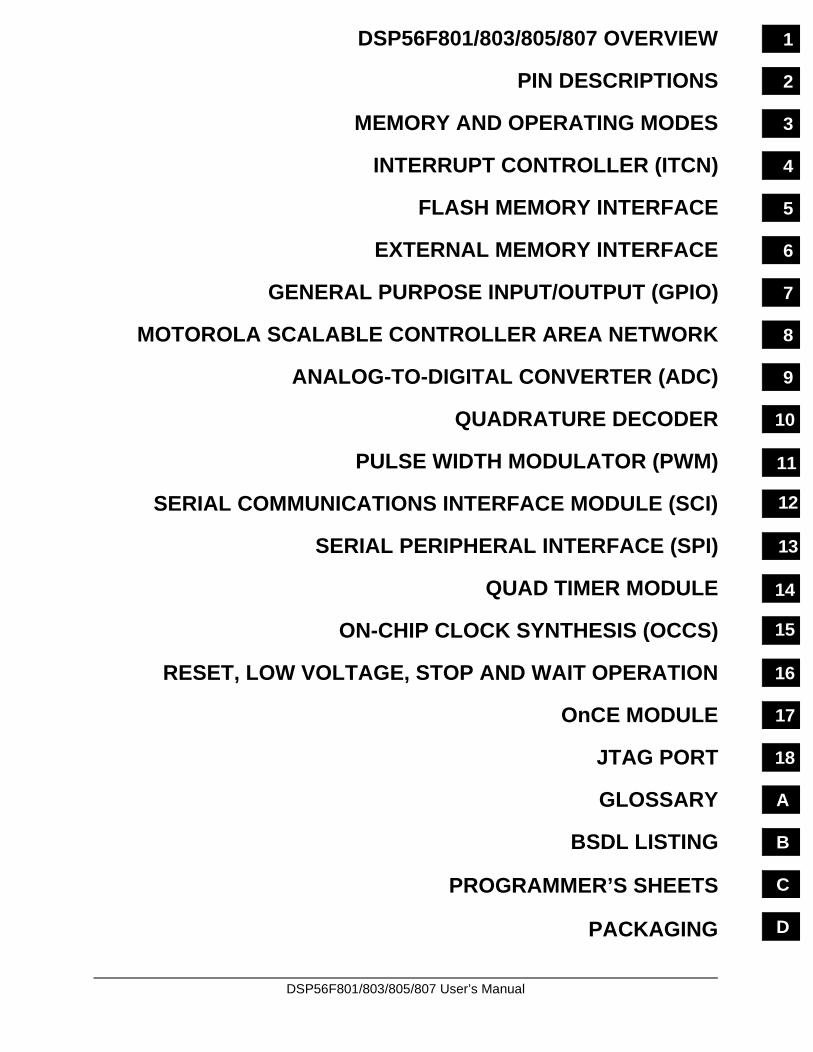
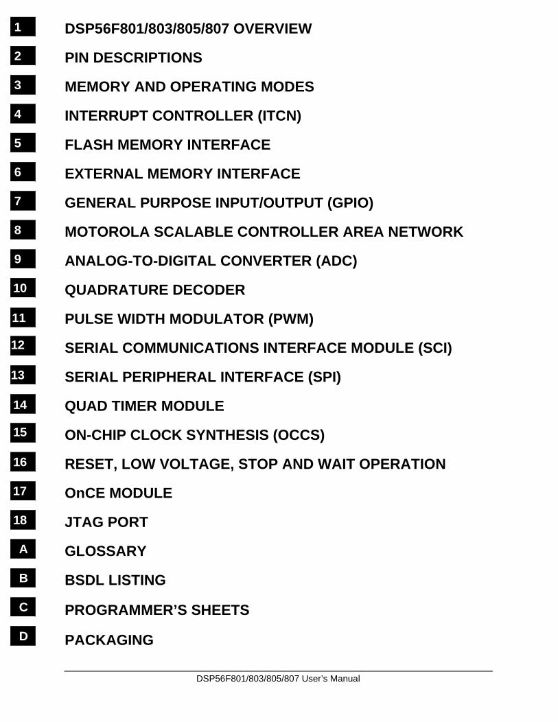
DSP56F801/803/805/807 OVERVIEW
PIN DESCRIPTIONS
MEMORY AND OPERATING MODES
INTERRUPT CONTROLLER (ITCN)
FLASH MEMORY INTERFACE
EXTERNAL MEMORY INTERFACE
GENERAL PURPOSE INPUT/OUTPUT (GPIO)
MOTOROLA SCALABLE CONTROLLER AREA NETWORK
ANALOG-TO-DIGITAL CONVERTER (ADC)
QUADRATURE DECODER
PULSE WIDTH MODULATOR (PWM)
SERIAL COMMUNICATIONS INTERFACE MODULE (SCI)
SERIAL PERIPHERAL INTERFACE (SPI)
QUAD TIMER MODULE
ON-CHIP CLOCK SYNTHESIS (OCCS)
RESET, LOW VOLTAGE, STOP AND WAIT OPERATION
OnCE MODULE
JTAG PORT
GLOSSARY
BSDL LISTING
PROGRAMMER’S SHEETS
PACKAGING
15
DSP56F801/803/805/807 User’s Manual
DSP56F801/803/805/807 OVERVIEW
PIN DESCRIPTIONS
MEMORY AND OPERATING MODES
INTERRUPT CONTROLLER (ITCN)
FLASH MEMORY INTERFACE
EXTERNAL MEMORY INTERFACE
GENERAL PURPOSE INPUT/OUTPUT (GPIO)
MOTOROLA SCALABLE CONTROLLER AREA NETWORK
ANALOG-TO-DIGITAL CONVERTER (ADC)
QUADRATURE DECODER
PULSE WIDTH MODULATOR (PWM)
SERIAL COMMUNICATIONS INTERFACE MODULE (SCI)
SERIAL PERIPHERAL INTERFACE (SPI)
QUAD TIMER MODULE
ON-CHIP CLOCK SYNTHESIS (OCCS)
RESET, LOW VOLTAGE, STOP AND WAIT OPERATION
OnCE MODULE
JTAG PORT
GLOSSARY
BSDL LISTING
PROGRAMMER’S SHEETS
PACKAGING
1
10
5
4
3
2
8
9
6
7
13
12
11
N
A
ON
B
18
17
16
14
C
D
15
�DSP56F801/803/805/807 User’s Manual i
Preliminary
TABLE OF CONTENTS
Chapter 1 DSP56F801/803/805/807 Overview1.1 Introduction . . . . . . . . . . . . . . . . . . . . . . . . . . . . . . . . . . . . . . . . . . . . . . . . . . . . 1-31.2 DSP56800 Family Description . . . . . . . . . . . . . . . . . . . . . . . . . . . . . . . . . . . . . 1-51.3 Manual Organization . . . . . . . . . . . . . . . . . . . . . . . . . . . . . . . . . . . . . . . . . . . . . 1-71.4 Manual Conventions . . . . . . . . . . . . . . . . . . . . . . . . . . . . . . . . . . . . . . . . . . . . . 1-91.5 Architectural Overview . . . . . . . . . . . . . . . . . . . . . . . . . . . . . . . . . . . . . . . . . . 1-111.6 DSP56800 Core Description . . . . . . . . . . . . . . . . . . . . . . . . . . . . . . . . . . . . . . 1-161.6.1 DSP56800 Core Differences . . . . . . . . . . . . . . . . . . . . . . . . . . . . . . . . . . . 1-161.6.2 DSP56800 Core Block Diagram . . . . . . . . . . . . . . . . . . . . . . . . . . . . . . . . 1-171.6.3 Data Arithmetic Logic Unit (Data ALU) . . . . . . . . . . . . . . . . . . . . . . . . . . . 1-201.6.4 Address Generation Unit (AGU) . . . . . . . . . . . . . . . . . . . . . . . . . . . . . . . . 1-211.6.5 Program Controller and Hardware Looping Unit . . . . . . . . . . . . . . . . . . . . 1-211.6.6 Bit Manipulation Unit . . . . . . . . . . . . . . . . . . . . . . . . . . . . . . . . . . . . . . . . . 1-211.6.7 Address and Data Buses . . . . . . . . . . . . . . . . . . . . . . . . . . . . . . . . . . . . . . 1-221.6.8 On-Chip Emulation (OnCE) Module. . . . . . . . . . . . . . . . . . . . . . . . . . . . . . 1-231.6.9 On-Chip Clock Synthesis Block . . . . . . . . . . . . . . . . . . . . . . . . . . . . . . . . . 1-231.6.10 Oscillators . . . . . . . . . . . . . . . . . . . . . . . . . . . . . . . . . . . . . . . . . . . . . . . . . 1-231.6.11 PLL. . . . . . . . . . . . . . . . . . . . . . . . . . . . . . . . . . . . . . . . . . . . . . . . . . . . . . . 1-241.6.12 Resets . . . . . . . . . . . . . . . . . . . . . . . . . . . . . . . . . . . . . . . . . . . . . . . . . . . . 1-241.6.13 Core Voltage Regulator . . . . . . . . . . . . . . . . . . . . . . . . . . . . . . . . . . . . . . . 1-251.6.14 IPBus Bridge . . . . . . . . . . . . . . . . . . . . . . . . . . . . . . . . . . . . . . . . . . . . . . . 1-251.7 Memory Modules. . . . . . . . . . . . . . . . . . . . . . . . . . . . . . . . . . . . . . . . . . . . . . . 1-251.7.1 Program Flash . . . . . . . . . . . . . . . . . . . . . . . . . . . . . . . . . . . . . . . . . . . . . . 1-261.7.2 Program RAM . . . . . . . . . . . . . . . . . . . . . . . . . . . . . . . . . . . . . . . . . . . . . . 1-271.7.3 Data Flash . . . . . . . . . . . . . . . . . . . . . . . . . . . . . . . . . . . . . . . . . . . . . . . . . 1-271.7.4 Data RAM . . . . . . . . . . . . . . . . . . . . . . . . . . . . . . . . . . . . . . . . . . . . . . . . . 1-271.8 DSP56F801 Peripheral Blocks . . . . . . . . . . . . . . . . . . . . . . . . . . . . . . . . . . . . 1-271.9 DSP56F803 Peripheral Blocks . . . . . . . . . . . . . . . . . . . . . . . . . . . . . . . . . . . . 1-281.10 DSP56F805 Peripheral Blocks . . . . . . . . . . . . . . . . . . . . . . . . . . . . . . . . . . . . 1-291.11 DSP56F807 Peripheral Blocks . . . . . . . . . . . . . . . . . . . . . . . . . . . . . . . . . . . . 1-291.12 Peripheral Descriptions . . . . . . . . . . . . . . . . . . . . . . . . . . . . . . . . . . . . . . . . . . 1-301.12.1 External Memory Interface. . . . . . . . . . . . . . . . . . . . . . . . . . . . . . . . . . . . . 1-301.12.2 General Purpose Input/Output Port (GPIO) . . . . . . . . . . . . . . . . . . . . . . . . 1-301.12.3 Serial Peripheral Interface (SPI) . . . . . . . . . . . . . . . . . . . . . . . . . . . . . . . . 1-311.12.4 COP/Watchdog Timer & Modes of Operation Module . . . . . . . . . . . . . . . . 1-311.12.5 JTAG/OnCE Port . . . . . . . . . . . . . . . . . . . . . . . . . . . . . . . . . . . . . . . . . . . . 1-321.12.6 Quadrature Decoder . . . . . . . . . . . . . . . . . . . . . . . . . . . . . . . . . . . . . . . . . 1-32
ii DSP56F801/803/805/807 User’s Manual�Preliminary
1.12.7 Quad Timer Module . . . . . . . . . . . . . . . . . . . . . . . . . . . . . . . . . . . . . . . . . . 1-331.12.8 Pulse Width Modulator (PWM) Module . . . . . . . . . . . . . . . . . . . . . . . . . . . 1-331.12.9 Analog-to-Digital Conversion (ADC) . . . . . . . . . . . . . . . . . . . . . . . . . . . . . 1-341.12.10 ADC & PWM Synchronization Feature . . . . . . . . . . . . . . . . . . . . . . . . . . . 1-351.12.11 Serial Communications Interface (SCI) . . . . . . . . . . . . . . . . . . . . . . . . . . . 1-351.12.12 Motorola Scannable Controller Area Network (MSCAN) Module. . . . . . . . 1-351.12.13 Peripheral Interrupts . . . . . . . . . . . . . . . . . . . . . . . . . . . . . . . . . . . . . . . . . 1-361.13 DSP56800 Programming Model . . . . . . . . . . . . . . . . . . . . . . . . . . . . . . . . . . . 1-36
Chapter 2 Pin Descriptions2.1 Introduction . . . . . . . . . . . . . . . . . . . . . . . . . . . . . . . . . . . . . . . . . . . . . . . . . . . . 2-32.2 Power and Ground Signals . . . . . . . . . . . . . . . . . . . . . . . . . . . . . . . . . . . . . . . . 2-82.3 Clock and Phase Lock Loop Signals . . . . . . . . . . . . . . . . . . . . . . . . . . . . . . . . 2-112.4 Address, Data, and Bus Control Signals . . . . . . . . . . . . . . . . . . . . . . . . . . . . . 2-122.5 Interrupt and Program Control Signals . . . . . . . . . . . . . . . . . . . . . . . . . . . . . . 2-142.6 GPIO Signals. . . . . . . . . . . . . . . . . . . . . . . . . . . . . . . . . . . . . . . . . . . . . . . . . . 2-152.7 Pulse Width Modulator (PWM) Signals . . . . . . . . . . . . . . . . . . . . . . . . . . . . . . 2-162.8 Serial Peripheral Interface (SPI) Signals . . . . . . . . . . . . . . . . . . . . . . . . . . . . . 2-172.9 Quadrature Decoder Signals . . . . . . . . . . . . . . . . . . . . . . . . . . . . . . . . . . . . . . 2-182.10 Serial Communications Interface (SCI) Signals . . . . . . . . . . . . . . . . . . . . . . . 2-192.11 CAN Signals . . . . . . . . . . . . . . . . . . . . . . . . . . . . . . . . . . . . . . . . . . . . . . . . . . 2-192.12 Analog to Digital Converter (ADC) Signals . . . . . . . . . . . . . . . . . . . . . . . . . . . 2-202.13 Quad Timer Module Signals . . . . . . . . . . . . . . . . . . . . . . . . . . . . . . . . . . . . . . 2-202.14 JTAG/OnCE . . . . . . . . . . . . . . . . . . . . . . . . . . . . . . . . . . . . . . . . . . . . . . . . . . 2-21
Chapter 3 Memory and Operating Modes3.1 Memory Map . . . . . . . . . . . . . . . . . . . . . . . . . . . . . . . . . . . . . . . . . . . . . . . . . . . 3-33.2 DSP56F801/803/805/807 Memory Map Description. . . . . . . . . . . . . . . . . . . . . 3-33.3 Data Memory. . . . . . . . . . . . . . . . . . . . . . . . . . . . . . . . . . . . . . . . . . . . . . . . . . . 3-53.3.1 Bus Control Register (BCR). . . . . . . . . . . . . . . . . . . . . . . . . . . . . . . . . . . . . 3-73.3.1.1 Reserved Bits—Bits 15–10 and 8. . . . . . . . . . . . . . . . . . . . . . . . . . . . . . 3-73.3.1.2 Drive Bit (DRV)—Bit 9 . . . . . . . . . . . . . . . . . . . . . . . . . . . . . . . . . . . . . . 3-73.3.1.3 Wait State Data Memory (WSX[3:0])—Bits 7–4 . . . . . . . . . . . . . . . . . . . 3-83.3.1.4 Wait State P Memory (WSP[3:0])—Bits 3–0. . . . . . . . . . . . . . . . . . . . . . 3-83.3.2 Operating Mode Register (OMR) . . . . . . . . . . . . . . . . . . . . . . . . . . . . . . . . . 3-83.3.2.1 Nested Looping (NL)—Bit 15 . . . . . . . . . . . . . . . . . . . . . . . . . . . . . . . . . 3-93.3.2.2 Reserved Bits—Bits 14–9, 7 and 2. . . . . . . . . . . . . . . . . . . . . . . . . . . . . 3-93.3.2.3 Condition Codes (CC)—Bit 8 . . . . . . . . . . . . . . . . . . . . . . . . . . . . . . . . . 3-93.3.2.4 Stop Delay (SD)—Bit 6 . . . . . . . . . . . . . . . . . . . . . . . . . . . . . . . . . . . . . 3-103.3.2.5 Rounding (R)—Bit 5 . . . . . . . . . . . . . . . . . . . . . . . . . . . . . . . . . . . . . . . 3-10
�Table of Contents iii
Preliminary
3.3.2.6 Saturation (SA)—Bit 4 . . . . . . . . . . . . . . . . . . . . . . . . . . . . . . . . . . . . . 3-103.3.2.7 External X Memory (EX)—Bit 3 . . . . . . . . . . . . . . . . . . . . . . . . . . . . . . 3-113.3.2.8 Operating Mode B (MB)—Bit 1. . . . . . . . . . . . . . . . . . . . . . . . . . . . . . . 3-113.3.2.9 Operating Mode A (MA)—Bit 0. . . . . . . . . . . . . . . . . . . . . . . . . . . . . . . 3-113.4 Core Configuration Memory Map . . . . . . . . . . . . . . . . . . . . . . . . . . . . . . . . . . 3-113.5 On-Chip Peripheral Memory Map . . . . . . . . . . . . . . . . . . . . . . . . . . . . . . . . . . 3-123.6 Program Memory . . . . . . . . . . . . . . . . . . . . . . . . . . . . . . . . . . . . . . . . . . . . . . 3-283.7 DSP56800 Operating Modes . . . . . . . . . . . . . . . . . . . . . . . . . . . . . . . . . . . . . 3-293.7.1 Single Chip Mode: Start-up (Mode 0) . . . . . . . . . . . . . . . . . . . . . . . . . . . . 3-293.7.2 Modes 1 & 2. . . . . . . . . . . . . . . . . . . . . . . . . . . . . . . . . . . . . . . . . . . . . . . . 3-303.7.3 External Mode (Mode 3) . . . . . . . . . . . . . . . . . . . . . . . . . . . . . . . . . . . . . . 3-303.8 Boot Flash Operation . . . . . . . . . . . . . . . . . . . . . . . . . . . . . . . . . . . . . . . . . . . 3-303.9 Executing Programs from XRAM . . . . . . . . . . . . . . . . . . . . . . . . . . . . . . . . . . 3-323.10 DSP56800 Reset and Interrupt Vectors . . . . . . . . . . . . . . . . . . . . . . . . . . . . . 3-323.11 Memory Architecture . . . . . . . . . . . . . . . . . . . . . . . . . . . . . . . . . . . . . . . . . . . . 3-35
Chapter 4 Interrupt Controller (ITCN)4.1 Introduction . . . . . . . . . . . . . . . . . . . . . . . . . . . . . . . . . . . . . . . . . . . . . . . . . . . . 4-34.2 DSP56F801/803/805/807 Interrupt Priority Register (IPR) . . . . . . . . . . . . . . . . 4-44.3 ITCN Register Summary . . . . . . . . . . . . . . . . . . . . . . . . . . . . . . . . . . . . . . . . . . 4-54.4 Priority Level and Vector Assignments . . . . . . . . . . . . . . . . . . . . . . . . . . . . . . . 4-64.5 Register Definitions . . . . . . . . . . . . . . . . . . . . . . . . . . . . . . . . . . . . . . . . . . . . . . 4-94.5.1 Group Priority Registers 2–15 (GPR2–GPR15) . . . . . . . . . . . . . . . . . . . . . 4-94.5.2 Test Interrupt Request Registers 0-3 (TIRQO-TIQ3). . . . . . . . . . . . . . . . . 4-134.5.3 Test Interrupt Source Registers 0–3 (TISR0–TISR3) . . . . . . . . . . . . . . . . 4-144.5.4 Test Control and Status Register (TCSR) . . . . . . . . . . . . . . . . . . . . . . . . . 4-144.5.4.1 Any IRQ Flag Bit (IRQ0)—Bit 15 . . . . . . . . . . . . . . . . . . . . . . . . . . . . . 4-144.5.4.2 Current Vector Output (vector[5:0])—Bits 13–8 . . . . . . . . . . . . . . . . . . 4-154.5.4.3 Test Mode (TMODE)—Bit 7 . . . . . . . . . . . . . . . . . . . . . . . . . . . . . . . . . 4-154.5.4.4 Peripheral Test Mode (PTM)—Bit 6 . . . . . . . . . . . . . . . . . . . . . . . . . . . 4-154.5.4.5 Field Specifying the Interrupt Acknowledge Level During PTM
(tst_iack[2:0])—Bits 2–0 . . . . . . . . . . . . . . . . . . . . . . . . . . . . . . . . . 4-15
Chapter 5 Flash Memory Interface5.1 Introduction . . . . . . . . . . . . . . . . . . . . . . . . . . . . . . . . . . . . . . . . . . . . . . . . . . . . 5-35.2 Features . . . . . . . . . . . . . . . . . . . . . . . . . . . . . . . . . . . . . . . . . . . . . . . . . . . . . . 5-35.3 Register Summary . . . . . . . . . . . . . . . . . . . . . . . . . . . . . . . . . . . . . . . . . . . . . . 5-35.4 General Flash Description. . . . . . . . . . . . . . . . . . . . . . . . . . . . . . . . . . . . . . . . . 5-55.4.1 Flash Timing Relationships . . . . . . . . . . . . . . . . . . . . . . . . . . . . . . . . . . . . . 5-8
iv DSP56F801/803/805/807 User’s Manual�Preliminary
5.5 Program Flash (PFLASH) . . . . . . . . . . . . . . . . . . . . . . . . . . . . . . . . . . . . . . . . . 5-95.5.1 Program Flash Block Diagram . . . . . . . . . . . . . . . . . . . . . . . . . . . . . . . . . . 5-105.6 Data Flash (DFLASH) . . . . . . . . . . . . . . . . . . . . . . . . . . . . . . . . . . . . . . . . . . . 5-105.6.1 Data Flash Block Diagram . . . . . . . . . . . . . . . . . . . . . . . . . . . . . . . . . . . . . 5-115.7 Boot Flash (BFLASH) . . . . . . . . . . . . . . . . . . . . . . . . . . . . . . . . . . . . . . . . . . . 5-115.7.1 Boot Flash Block Diagram . . . . . . . . . . . . . . . . . . . . . . . . . . . . . . . . . . . . . 5-125.8 Program/Data/Boot Flash Interface Unit Features . . . . . . . . . . . . . . . . . . . . . 5-125.9 Program/Data/Boot Flash Modes . . . . . . . . . . . . . . . . . . . . . . . . . . . . . . . . . . 5-125.10 Functional Description of the PFIU, DFIU and BFIU . . . . . . . . . . . . . . . . . . . . 5-135.11 Flash Programming and Erase Models . . . . . . . . . . . . . . . . . . . . . . . . . . . . . . 5-145.11.1 Intelligent Word Programming . . . . . . . . . . . . . . . . . . . . . . . . . . . . . . . . . . 5-145.11.2 Dumb Word Programming . . . . . . . . . . . . . . . . . . . . . . . . . . . . . . . . . . . . . 5-155.11.3 Intelligent Erase Operation . . . . . . . . . . . . . . . . . . . . . . . . . . . . . . . . . . . . 5-165.11.4 Memory Map & Register Definitions. . . . . . . . . . . . . . . . . . . . . . . . . . . . . . 5-165.11.4.1 Flash Control Register (FIU_CNTL) . . . . . . . . . . . . . . . . . . . . . . . . . . . 5-175.11.4.2 Flash Program Enable Register (FIU_PE) . . . . . . . . . . . . . . . . . . . . . . 5-185.11.4.3 Flash Erase Enable Register (FIU_EE) . . . . . . . . . . . . . . . . . . . . . . . . 5-195.11.4.4 Flash Address Register (FIU_ADDR). . . . . . . . . . . . . . . . . . . . . . . . . . 5-205.11.4.5 Flash Data Register (FIU_DATA) . . . . . . . . . . . . . . . . . . . . . . . . . . . . . 5-215.11.4.6 Flash Interrupt Enable Register (FIU_IE) . . . . . . . . . . . . . . . . . . . . . . . 5-215.11.4.7 Flash Interrupt Source Register (FIU_IS) . . . . . . . . . . . . . . . . . . . . . . . 5-225.11.4.8 Flash Interrupt Pending Register (FIU_IP) . . . . . . . . . . . . . . . . . . . . . . 5-235.11.4.9 Flash Clock Divisor Register (FIU_CKDIVISOR) . . . . . . . . . . . . . . . . . 5-245.11.4.10 Flash Terase Limit Register (FIU_TERASEL) . . . . . . . . . . . . . . . . . . . 5-245.11.4.11 Flash Tme Limit Register (FIU_TMEL) . . . . . . . . . . . . . . . . . . . . . . . . . 5-255.11.4.12 Flash Tnvs Limit Register (FIU_TNVSL) . . . . . . . . . . . . . . . . . . . . . . . 5-255.11.4.13 Flash Tpgs Limit Register (FIU_TPGSL) . . . . . . . . . . . . . . . . . . . . . . . 5-265.11.4.14 Flash Tprog Limit Register (FIU_TPROGL) . . . . . . . . . . . . . . . . . . . . . 5-265.11.4.15 Flash Tnvh Limit Register (FIU_TNVHL) . . . . . . . . . . . . . . . . . . . . . . . 5-275.11.4.16 Flash Tnvh1 Limit Register (FIU_TNVH1L) . . . . . . . . . . . . . . . . . . . . . 5-275.11.4.17 Flash Trcv Limit Register (FIU_TRCVL) . . . . . . . . . . . . . . . . . . . . . . . . 5-285.11.4.18 Flash Interface Unit Timeout Registers . . . . . . . . . . . . . . . . . . . . . . . . 5-28
Chapter 6 External Memory Interface6.1 Introduction . . . . . . . . . . . . . . . . . . . . . . . . . . . . . . . . . . . . . . . . . . . . . . . . . . . . 6-36.2 External Memory Port Architecture . . . . . . . . . . . . . . . . . . . . . . . . . . . . . . . . . . 6-36.3 Pin Descriptions . . . . . . . . . . . . . . . . . . . . . . . . . . . . . . . . . . . . . . . . . . . . . . . . 6-36.4 Register Summary. . . . . . . . . . . . . . . . . . . . . . . . . . . . . . . . . . . . . . . . . . . . . . . 6-46.5 Port A Description . . . . . . . . . . . . . . . . . . . . . . . . . . . . . . . . . . . . . . . . . . . . . . . 6-46.5.1 Reserved Bits—Bits 15–10 and 8 . . . . . . . . . . . . . . . . . . . . . . . . . . . . . . . . 6-46.5.2 Drive (DRV)—Bit 9 . . . . . . . . . . . . . . . . . . . . . . . . . . . . . . . . . . . . . . . . . . . . 6-4
�Table of Contents v
Preliminary
6.5.3 Wait State X Data Memory (WSX[3:0])—Bits 7–4 . . . . . . . . . . . . . . . . . . . . 6-56.5.4 Wait State P Memory (WSP[3:0])—Bits 3–0 . . . . . . . . . . . . . . . . . . . . . . . . 6-56.5.5 Pins in Different Processing States . . . . . . . . . . . . . . . . . . . . . . . . . . . . . . . 6-7
Chapter 7 General Purpose Input/Output (GPIO)7.1 Introduction . . . . . . . . . . . . . . . . . . . . . . . . . . . . . . . . . . . . . . . . . . . . . . . . . . . . 7-37.2 GPIO Interrupts . . . . . . . . . . . . . . . . . . . . . . . . . . . . . . . . . . . . . . . . . . . . . . . . . 7-67.3 GPIO Register Summary . . . . . . . . . . . . . . . . . . . . . . . . . . . . . . . . . . . . . . . . . 7-77.4 Chip Specific Configurations . . . . . . . . . . . . . . . . . . . . . . . . . . . . . . . . . . . . . . . 7-97.5 Programming Model . . . . . . . . . . . . . . . . . . . . . . . . . . . . . . . . . . . . . . . . . . . . . 7-97.5.1 Pull-Up Enable Register (PUR) . . . . . . . . . . . . . . . . . . . . . . . . . . . . . . . . . 7-107.5.2 Data Register (DR) . . . . . . . . . . . . . . . . . . . . . . . . . . . . . . . . . . . . . . . . . . 7-107.5.3 Data Direction Register (DDR) . . . . . . . . . . . . . . . . . . . . . . . . . . . . . . . . . 7-107.5.4 Peripheral Enable Register (PER) . . . . . . . . . . . . . . . . . . . . . . . . . . . . . . . 7-117.5.5 Interrupt Assert Register (IAR) . . . . . . . . . . . . . . . . . . . . . . . . . . . . . . . . . 7-117.5.6 Interrupt Enable Register (IENR). . . . . . . . . . . . . . . . . . . . . . . . . . . . . . . . 7-127.5.7 Interrupt Polarity Register (IPOLR) . . . . . . . . . . . . . . . . . . . . . . . . . . . . . . 7-127.5.8 Interrupt Pending Register (IPR) . . . . . . . . . . . . . . . . . . . . . . . . . . . . . . . . 7-127.5.9 Interrupt Edge Sensitive Register (IESR) . . . . . . . . . . . . . . . . . . . . . . . . . 7-137.6 GPIO Programming Algorithms. . . . . . . . . . . . . . . . . . . . . . . . . . . . . . . . . . . . 7-13
Chapter 8 Motorola Scalable Controller Area Network (MSCAN)8.1 Introduction . . . . . . . . . . . . . . . . . . . . . . . . . . . . . . . . . . . . . . . . . . . . . . . . . . . . 8-38.2 Features . . . . . . . . . . . . . . . . . . . . . . . . . . . . . . . . . . . . . . . . . . . . . . . . . . . . . . 8-48.3 Pin Definitions . . . . . . . . . . . . . . . . . . . . . . . . . . . . . . . . . . . . . . . . . . . . . . . . . . 8-48.4 Block Diagram. . . . . . . . . . . . . . . . . . . . . . . . . . . . . . . . . . . . . . . . . . . . . . . . . . 8-68.5 Register Summary . . . . . . . . . . . . . . . . . . . . . . . . . . . . . . . . . . . . . . . . . . . . . . 8-68.6 Register Map. . . . . . . . . . . . . . . . . . . . . . . . . . . . . . . . . . . . . . . . . . . . . . . . . . . 8-78.7 Functional Description. . . . . . . . . . . . . . . . . . . . . . . . . . . . . . . . . . . . . . . . . . . 8-108.7.1 Message Storage. . . . . . . . . . . . . . . . . . . . . . . . . . . . . . . . . . . . . . . . . . . . 8-108.7.1.1 Message Transmit Background . . . . . . . . . . . . . . . . . . . . . . . . . . . . . . 8-128.7.1.2 Transmit Structures . . . . . . . . . . . . . . . . . . . . . . . . . . . . . . . . . . . . . . . 8-128.7.1.3 Receive Structures . . . . . . . . . . . . . . . . . . . . . . . . . . . . . . . . . . . . . . . . 8-138.7.1.4 Identifier Acceptance Filter. . . . . . . . . . . . . . . . . . . . . . . . . . . . . . . . . . 8-148.7.2 Protocol Violation Protection . . . . . . . . . . . . . . . . . . . . . . . . . . . . . . . . . . . 8-188.7.3 Clock System. . . . . . . . . . . . . . . . . . . . . . . . . . . . . . . . . . . . . . . . . . . . . . . 8-188.8 Register Descriptions . . . . . . . . . . . . . . . . . . . . . . . . . . . . . . . . . . . . . . . . . . . 8-218.8.1 MSCAN Control Register 0 (CANCTL0) . . . . . . . . . . . . . . . . . . . . . . . . . . 8-228.8.1.1 Reserved Bits—Bits 15–8 . . . . . . . . . . . . . . . . . . . . . . . . . . . . . . . . . . 8-228.8.1.2 Received Frame Flag (RXFRM)—Bit 7 . . . . . . . . . . . . . . . . . . . . . . . . 8-22
vi DSP56F801/803/805/807 User’s Manual�Preliminary
8.8.1.3 Receiver Active Status (RXACT)—Bit 6 . . . . . . . . . . . . . . . . . . . . . . . . 8-228.8.1.4 CAN Stops in Wait Mode (CSWAI)—Bit 5 . . . . . . . . . . . . . . . . . . . . . . 8-228.8.1.5 Synchronized Status (SYNCH)—Bit 4 . . . . . . . . . . . . . . . . . . . . . . . . . 8-238.8.1.6 Reserved Bit—Bit 3 . . . . . . . . . . . . . . . . . . . . . . . . . . . . . . . . . . . . . . . 8-238.8.1.7 Sleep Acknowledge (SLPAK)—Bit 2 . . . . . . . . . . . . . . . . . . . . . . . . . . 8-238.8.1.8 Sleep Request–Go into Sleep Mode (SLPRQ)—Bit 1 . . . . . . . . . . . . . 8-238.8.1.9 Soft Reset (SFTRES)—Bit 0. . . . . . . . . . . . . . . . . . . . . . . . . . . . . . . . . 8-238.8.2 MSCAN Control Register 1 (CANCTL1) . . . . . . . . . . . . . . . . . . . . . . . . . . 8-248.8.2.1 Reserved Bits—Bits 15–8 and 6–3. . . . . . . . . . . . . . . . . . . . . . . . . . . . 8-248.8.2.2 CAN Enable (CANE)—Bit 7 . . . . . . . . . . . . . . . . . . . . . . . . . . . . . . . . . 8-248.8.2.3 Loop Back Self Test Mode (LOOPB)—Bit 2 . . . . . . . . . . . . . . . . . . . . . 8-258.8.2.4 Wake-Up Mode (WUPM)—Bit 1 . . . . . . . . . . . . . . . . . . . . . . . . . . . . . . 8-258.8.2.5 MSCAN Clock Source (CLKSRC)—Bit 0 . . . . . . . . . . . . . . . . . . . . . . . 8-258.8.3 MSCAN Bus Timing Register 0 (CANBTR0) . . . . . . . . . . . . . . . . . . . . . . . 8-258.8.3.1 Reserved Bits—Bits 15–8. . . . . . . . . . . . . . . . . . . . . . . . . . . . . . . . . . . 8-268.8.3.2 Synchronization Jump Width (SJW[1:0])—Bits 7–6 . . . . . . . . . . . . . . . 8-268.8.3.3 Baud Rate Prescaler (BRP[5:0])—Bits 5–0 . . . . . . . . . . . . . . . . . . . . . 8-268.8.4 MSCAN Bus Timing Register 1 (CANBTR1) . . . . . . . . . . . . . . . . . . . . . . . 8-278.8.4.1 Reserved Bits—Bits 15–8. . . . . . . . . . . . . . . . . . . . . . . . . . . . . . . . . . . 8-278.8.4.2 Sampling (SAMP)—Bit 7 . . . . . . . . . . . . . . . . . . . . . . . . . . . . . . . . . . . 8-278.8.4.3 Time Segment 2 (TSEG22–TSEG20)—Bits 6–4 . . . . . . . . . . . . . . . . . 8-288.8.4.4 Time Segment 1 (TSEG13–TSEG10)—Bits 3–0 . . . . . . . . . . . . . . . . . 8-288.8.5 MSCAN Receiver Flag Register (CANRFLG) . . . . . . . . . . . . . . . . . . . . . . 8-298.8.5.1 Reserved Bits—Bits 15–8. . . . . . . . . . . . . . . . . . . . . . . . . . . . . . . . . . . 8-308.8.5.2 Wake-up Interrupt Flag (WUPIF)—Bit 7 . . . . . . . . . . . . . . . . . . . . . . . . 8-308.8.5.3 Receiver Warning Interrupt Flag (RWRNIF)—Bit 6 . . . . . . . . . . . . . . . 8-308.8.5.4 Transmitter Warning Interrupt Flag (TWRNIF)—Bit 5. . . . . . . . . . . . . . 8-308.8.5.5 Receiver Error Passive Interrupt Flag (RERRIF)—Bit 4 . . . . . . . . . . . . 8-308.8.5.6 Transmitter Error Passive Interrupt Flag (TERRIF)—Bit 3 . . . . . . . . . . 8-318.8.5.7 Bus-Off Interrupt Flag (BOFFIF)—Bit 2 . . . . . . . . . . . . . . . . . . . . . . . . 8-318.8.5.8 Overrun Interrupt Flag (OVRIF)—Bit 1 . . . . . . . . . . . . . . . . . . . . . . . . . 8-318.8.5.9 Receive Buffer Full (RXF)—Bit 0 . . . . . . . . . . . . . . . . . . . . . . . . . . . . . 8-328.8.6 MSCAN Receiver Interrupt Enable Register (CANRIER) . . . . . . . . . . . . . 8-328.8.6.1 Reserved Bits—Bits 15–8. . . . . . . . . . . . . . . . . . . . . . . . . . . . . . . . . . . 8-328.8.6.2 Wake-up Interrupt Enable (WUPIE)—Bit 7. . . . . . . . . . . . . . . . . . . . . . 8-328.8.6.3 Receiver Warning Interrupt Enable (RWRNIE)—Bit 6 . . . . . . . . . . . . . 8-328.8.6.4 Transmitter Warning Interrupt Enable (TWRNIE)—Bit 5 . . . . . . . . . . . 8-338.8.6.5 Receiver Error Passive Interrupt Enable (RERRIE)—Bit 4. . . . . . . . . . 8-338.8.6.6 Transmitter Error Passive Interrupt Enable (TERRIE)—Bit 3 . . . . . . . . 8-338.8.6.7 Bus-Off Interrupt Enable (BOFFIE)—Bit 2 . . . . . . . . . . . . . . . . . . . . . . 8-338.8.6.8 Overrun Interrupt Enable (OVRIE)—Bit 1. . . . . . . . . . . . . . . . . . . . . . . 8-338.8.6.9 Receiver Full Interrupt Enable (RXFIE)—Bit 0 . . . . . . . . . . . . . . . . . . . 8-338.8.7 MSCAN Transmitter Flag Register (CANTFLG) . . . . . . . . . . . . . . . . . . . . 8-33
�Table of Contents vii
Preliminary
8.8.7.1 Reserved Bits—Bits 15–7 and 3 . . . . . . . . . . . . . . . . . . . . . . . . . . . . . 8-348.8.7.2 Abort Acknowledge (ABTAK[2:0])—Bits 6–4 . . . . . . . . . . . . . . . . . . . . 8-348.8.7.3 Transmitter Buffer Empty (TXE[2:0])—Bits 2–0 . . . . . . . . . . . . . . . . . . 8-348.8.8 MSCAN Transmitter Control Register (CANTCR) . . . . . . . . . . . . . . . . . . . 8-348.8.8.1 Reserved Bits—Bits 15–7 and 3 . . . . . . . . . . . . . . . . . . . . . . . . . . . . . 8-358.8.8.2 Abort Request (ABTRQ[2:0])—Bits 6–4 . . . . . . . . . . . . . . . . . . . . . . . . 8-358.8.8.3 Transmitter Empty Interrupt Enable (TXEIE[2:0])—Bits 2–0 . . . . . . . . 8-358.8.9 MSCAN Identifier Acceptance Control Register (CANIDAC). . . . . . . . . . . 8-358.8.9.1 Reserved Bits—Bits 15–6 and 3 . . . . . . . . . . . . . . . . . . . . . . . . . . . . . 8-368.8.9.2 Identifier Acceptance Mode (IDAM[1:0])—Bits 5–4 . . . . . . . . . . . . . . . 8-368.8.9.3 Identifier Acceptance Hit Indicator (IDHIT[2:0])—Bits 2–0 . . . . . . . . . . 8-368.8.10 MSCAN Receive Error Counter Register (CANRXERR) . . . . . . . . . . . . . . 8-378.8.11 MSCAN Transmit Error Counter Register (CANTXERR) . . . . . . . . . . . . . 8-378.8.12 MSCAN Identifier Acceptance Registers (CANIDAR0–7) . . . . . . . . . . . . . 8-388.8.12.1 Acceptance Code Bits (AC[7:0])—Bits 7–0 . . . . . . . . . . . . . . . . . . . . . 8-398.8.13 MSCAN Identifier Mask Registers (CANIDMR0–7) . . . . . . . . . . . . . . . . . . 8-398.8.13.1 Acceptance Mask Bits (AM[7:0])—Bits 7–0 . . . . . . . . . . . . . . . . . . . . . 8-408.8.14 Programmer’s Model of Message Storage . . . . . . . . . . . . . . . . . . . . . . . . 8-408.8.14.1 Identifier Registers (IDR0–3) . . . . . . . . . . . . . . . . . . . . . . . . . . . . . . . . 8-428.8.14.2 Data Segment Registers (DSR0–7) . . . . . . . . . . . . . . . . . . . . . . . . . . . 8-448.8.14.3 Data Length Register (DLR). . . . . . . . . . . . . . . . . . . . . . . . . . . . . . . . . 8-458.8.14.4 Transmit Buffer Priority Register (TBPR) . . . . . . . . . . . . . . . . . . . . . . . 8-468.9 Modes of Operation. . . . . . . . . . . . . . . . . . . . . . . . . . . . . . . . . . . . . . . . . . . . . 8-478.9.1 Normal Modes . . . . . . . . . . . . . . . . . . . . . . . . . . . . . . . . . . . . . . . . . . . . . . 8-478.9.2 Special Modes . . . . . . . . . . . . . . . . . . . . . . . . . . . . . . . . . . . . . . . . . . . . . . 8-478.9.3 Emulation Modes . . . . . . . . . . . . . . . . . . . . . . . . . . . . . . . . . . . . . . . . . . . . 8-478.9.4 Security Modes . . . . . . . . . . . . . . . . . . . . . . . . . . . . . . . . . . . . . . . . . . . . . 8-478.10 Low Power Options . . . . . . . . . . . . . . . . . . . . . . . . . . . . . . . . . . . . . . . . . . . . . 8-478.10.1 Run Mode . . . . . . . . . . . . . . . . . . . . . . . . . . . . . . . . . . . . . . . . . . . . . . . . . 8-488.10.2 Wait Mode . . . . . . . . . . . . . . . . . . . . . . . . . . . . . . . . . . . . . . . . . . . . . . . . . 8-488.10.3 Stop Mode . . . . . . . . . . . . . . . . . . . . . . . . . . . . . . . . . . . . . . . . . . . . . . . . . 8-498.10.4 Sleep Mode . . . . . . . . . . . . . . . . . . . . . . . . . . . . . . . . . . . . . . . . . . . . . . . . 8-498.10.5 Soft Reset Mode . . . . . . . . . . . . . . . . . . . . . . . . . . . . . . . . . . . . . . . . . . . . 8-528.10.6 Power Down Mode . . . . . . . . . . . . . . . . . . . . . . . . . . . . . . . . . . . . . . . . . . 8-528.10.7 Programmable Wake-Up Function . . . . . . . . . . . . . . . . . . . . . . . . . . . . . . 8-528.11 Interrupt Operation . . . . . . . . . . . . . . . . . . . . . . . . . . . . . . . . . . . . . . . . . . . . . 8-538.11.1 Interrupt Acknowledge . . . . . . . . . . . . . . . . . . . . . . . . . . . . . . . . . . . . . . . . 8-548.11.2 Interrupt Sources . . . . . . . . . . . . . . . . . . . . . . . . . . . . . . . . . . . . . . . . . . . . 8-558.11.3 Recovery from Stop or Wait. . . . . . . . . . . . . . . . . . . . . . . . . . . . . . . . . . . . 8-55
viii DSP56F801/803/805/807 User’s Manual�Preliminary
Chapter 9 Analog-to-Digital Converter (ADC)9.1 Introduction . . . . . . . . . . . . . . . . . . . . . . . . . . . . . . . . . . . . . . . . . . . . . . . . . . . . 9-39.2 Features . . . . . . . . . . . . . . . . . . . . . . . . . . . . . . . . . . . . . . . . . . . . . . . . . . . . . . 9-39.3 Functional Description. . . . . . . . . . . . . . . . . . . . . . . . . . . . . . . . . . . . . . . . . . . . 9-49.3.1 Differential Inputs . . . . . . . . . . . . . . . . . . . . . . . . . . . . . . . . . . . . . . . . . . . . . 9-59.4 Timing . . . . . . . . . . . . . . . . . . . . . . . . . . . . . . . . . . . . . . . . . . . . . . . . . . . . . . . . 9-89.5 Pin Descriptions . . . . . . . . . . . . . . . . . . . . . . . . . . . . . . . . . . . . . . . . . . . . . . . . 9-99.5.1 Analog Input Pins (AN0–AN7) . . . . . . . . . . . . . . . . . . . . . . . . . . . . . . . . . . . 9-99.5.2 Voltage Reference Pin (VREF) . . . . . . . . . . . . . . . . . . . . . . . . . . . . . . . . . 9-109.5.3 Supply Pins (VDDA, VSSA) . . . . . . . . . . . . . . . . . . . . . . . . . . . . . . . . . . . . 9-109.6 Register Summary. . . . . . . . . . . . . . . . . . . . . . . . . . . . . . . . . . . . . . . . . . . . . . 9-109.7 Register Definitions . . . . . . . . . . . . . . . . . . . . . . . . . . . . . . . . . . . . . . . . . . . . . 9-119.7.1 ADC Control Register 1 (ADCR1) . . . . . . . . . . . . . . . . . . . . . . . . . . . . . . . 9-119.7.1.1 Reserved Bits—Bits 15 and 3. . . . . . . . . . . . . . . . . . . . . . . . . . . . . . . . 9-119.7.1.2 Stop (STOP)—Bit 14 . . . . . . . . . . . . . . . . . . . . . . . . . . . . . . . . . . . . . . 9-119.7.1.3 START Conversion (START)—Bit 13. . . . . . . . . . . . . . . . . . . . . . . . . . 9-129.7.1.4 SYNC Select (SYNC)—Bit 12. . . . . . . . . . . . . . . . . . . . . . . . . . . . . . . . 9-129.7.1.5 End Of Scan Interrupt Enable (EOSIE)—Bit 11 . . . . . . . . . . . . . . . . . . 9-129.7.1.6 Zero Crossing Interrupt Enable (ZCIE)—Bit 10 . . . . . . . . . . . . . . . . . . 9-129.7.1.7 Low Limit Interrupt Enable (LLMTIE)—Bit 9 . . . . . . . . . . . . . . . . . . . . . 9-139.7.1.8 High Limit Interrupt Enable (HLMTIE)—Bit 8 . . . . . . . . . . . . . . . . . . . . 9-139.7.1.9 Channel Configure (CHNCFG[3:0])—Bits 7–4 . . . . . . . . . . . . . . . . . . . 9-139.7.1.10 Scan Mode (SMODE[2:0])—Bits 2–0 . . . . . . . . . . . . . . . . . . . . . . . . . . 9-139.7.2 ADC Control Register 2 (ADCR2) . . . . . . . . . . . . . . . . . . . . . . . . . . . . . . . 9-159.7.2.1 Reserved Bits—Bits 15–4. . . . . . . . . . . . . . . . . . . . . . . . . . . . . . . . . . . 9-159.7.2.2 Clock Divisor Select (DIV[3:0])—Bits 3–0. . . . . . . . . . . . . . . . . . . . . . . 9-159.7.3 ADC Zero Crossing Control Register (ADZCC) . . . . . . . . . . . . . . . . . . . . . 9-159.7.4 ADC Channel List Registers (ADLST1 & ADLST2) . . . . . . . . . . . . . . . . . . 9-169.7.5 ADC Sample Disable Register (ADSDIS) . . . . . . . . . . . . . . . . . . . . . . . . . 9-179.7.5.1 Test (TEST[1:0])—Bits 15–14. . . . . . . . . . . . . . . . . . . . . . . . . . . . . . . . 9-189.7.5.2 Reserved Bits—Bits 13–8. . . . . . . . . . . . . . . . . . . . . . . . . . . . . . . . . . . 9-189.7.5.3 Disable Sample (DS[7:0])—Bits 7–0. . . . . . . . . . . . . . . . . . . . . . . . . . . 9-189.7.6 ADC Status Register (ADSTAT) . . . . . . . . . . . . . . . . . . . . . . . . . . . . . . . . 9-189.7.6.1 Conversion in Progress (CIP)—Bit 15 . . . . . . . . . . . . . . . . . . . . . . . . . 9-199.7.6.2 Reserved Bits—Bits 14–12. . . . . . . . . . . . . . . . . . . . . . . . . . . . . . . . . . 9-199.7.6.3 End of Scan Interrupt (EOSI)—Bit 11. . . . . . . . . . . . . . . . . . . . . . . . . . 9-199.7.6.4 Zero Crossing Interrupt (ZCI)—Bit 10. . . . . . . . . . . . . . . . . . . . . . . . . . 9-199.7.6.5 Low Limit Interrupt (LLMTI)—Bit 9 . . . . . . . . . . . . . . . . . . . . . . . . . . . . 9-199.7.6.6 High Limit Interrupt (HLMTI)—Bit 8 . . . . . . . . . . . . . . . . . . . . . . . . . . . 9-209.7.6.7 Ready Channel 7–0 (RDY[7:0])—Bits 7–0 . . . . . . . . . . . . . . . . . . . . . . 9-209.7.7 ADC Limit Status Register (ADLSTAT) . . . . . . . . . . . . . . . . . . . . . . . . . . . 9-20
�Table of Contents ix
Preliminary
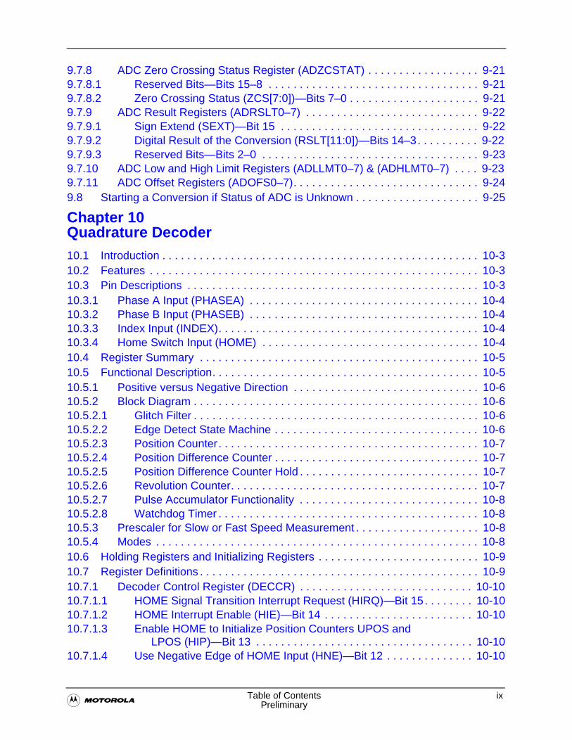
9.7.8 ADC Zero Crossing Status Register (ADZCSTAT) . . . . . . . . . . . . . . . . . . 9-219.7.8.1 Reserved Bits—Bits 15–8 . . . . . . . . . . . . . . . . . . . . . . . . . . . . . . . . . . 9-219.7.8.2 Zero Crossing Status (ZCS[7:0])—Bits 7–0 . . . . . . . . . . . . . . . . . . . . . 9-219.7.9 ADC Result Registers (ADRSLT0–7) . . . . . . . . . . . . . . . . . . . . . . . . . . . . 9-229.7.9.1 Sign Extend (SEXT)—Bit 15 . . . . . . . . . . . . . . . . . . . . . . . . . . . . . . . . 9-229.7.9.2 Digital Result of the Conversion (RSLT[11:0])—Bits 14–3. . . . . . . . . . 9-229.7.9.3 Reserved Bits—Bits 2–0 . . . . . . . . . . . . . . . . . . . . . . . . . . . . . . . . . . . 9-239.7.10 ADC Low and High Limit Registers (ADLLMT0–7) & (ADHLMT0–7) . . . . 9-239.7.11 ADC Offset Registers (ADOFS0–7). . . . . . . . . . . . . . . . . . . . . . . . . . . . . . 9-249.8 Starting a Conversion if Status of ADC is Unknown . . . . . . . . . . . . . . . . . . . . 9-25
Chapter 10 Quadrature Decoder10.1 Introduction . . . . . . . . . . . . . . . . . . . . . . . . . . . . . . . . . . . . . . . . . . . . . . . . . . . 10-310.2 Features . . . . . . . . . . . . . . . . . . . . . . . . . . . . . . . . . . . . . . . . . . . . . . . . . . . . . 10-310.3 Pin Descriptions . . . . . . . . . . . . . . . . . . . . . . . . . . . . . . . . . . . . . . . . . . . . . . . 10-310.3.1 Phase A Input (PHASEA) . . . . . . . . . . . . . . . . . . . . . . . . . . . . . . . . . . . . . 10-410.3.2 Phase B Input (PHASEB) . . . . . . . . . . . . . . . . . . . . . . . . . . . . . . . . . . . . . 10-410.3.3 Index Input (INDEX). . . . . . . . . . . . . . . . . . . . . . . . . . . . . . . . . . . . . . . . . . 10-410.3.4 Home Switch Input (HOME) . . . . . . . . . . . . . . . . . . . . . . . . . . . . . . . . . . . 10-410.4 Register Summary . . . . . . . . . . . . . . . . . . . . . . . . . . . . . . . . . . . . . . . . . . . . . 10-510.5 Functional Description. . . . . . . . . . . . . . . . . . . . . . . . . . . . . . . . . . . . . . . . . . . 10-510.5.1 Positive versus Negative Direction . . . . . . . . . . . . . . . . . . . . . . . . . . . . . . 10-610.5.2 Block Diagram . . . . . . . . . . . . . . . . . . . . . . . . . . . . . . . . . . . . . . . . . . . . . . 10-610.5.2.1 Glitch Filter . . . . . . . . . . . . . . . . . . . . . . . . . . . . . . . . . . . . . . . . . . . . . . 10-610.5.2.2 Edge Detect State Machine . . . . . . . . . . . . . . . . . . . . . . . . . . . . . . . . . 10-610.5.2.3 Position Counter. . . . . . . . . . . . . . . . . . . . . . . . . . . . . . . . . . . . . . . . . . 10-710.5.2.4 Position Difference Counter . . . . . . . . . . . . . . . . . . . . . . . . . . . . . . . . . 10-710.5.2.5 Position Difference Counter Hold . . . . . . . . . . . . . . . . . . . . . . . . . . . . . 10-710.5.2.6 Revolution Counter. . . . . . . . . . . . . . . . . . . . . . . . . . . . . . . . . . . . . . . . 10-710.5.2.7 Pulse Accumulator Functionality . . . . . . . . . . . . . . . . . . . . . . . . . . . . . 10-810.5.2.8 Watchdog Timer . . . . . . . . . . . . . . . . . . . . . . . . . . . . . . . . . . . . . . . . . . 10-810.5.3 Prescaler for Slow or Fast Speed Measurement . . . . . . . . . . . . . . . . . . . . 10-810.5.4 Modes . . . . . . . . . . . . . . . . . . . . . . . . . . . . . . . . . . . . . . . . . . . . . . . . . . . . 10-810.6 Holding Registers and Initializing Registers . . . . . . . . . . . . . . . . . . . . . . . . . . 10-910.7 Register Definitions . . . . . . . . . . . . . . . . . . . . . . . . . . . . . . . . . . . . . . . . . . . . . 10-910.7.1 Decoder Control Register (DECCR) . . . . . . . . . . . . . . . . . . . . . . . . . . . . 10-1010.7.1.1 HOME Signal Transition Interrupt Request (HIRQ)—Bit 15. . . . . . . . 10-1010.7.1.2 HOME Interrupt Enable (HIE)—Bit 14 . . . . . . . . . . . . . . . . . . . . . . . . 10-1010.7.1.3 Enable HOME to Initialize Position Counters UPOS and
LPOS (HIP)—Bit 13 . . . . . . . . . . . . . . . . . . . . . . . . . . . . . . . . . . . 10-1010.7.1.4 Use Negative Edge of HOME Input (HNE)—Bit 12 . . . . . . . . . . . . . . 10-10
x DSP56F801/803/805/807 User’s Manual�Preliminary
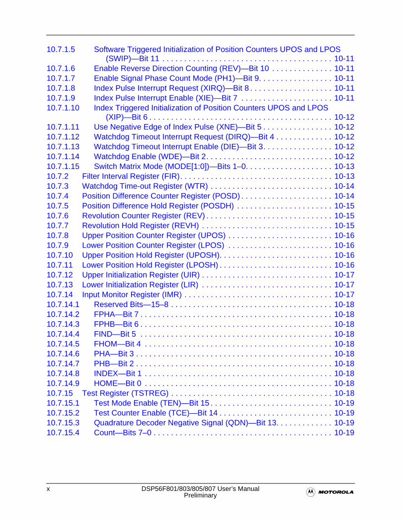
10.7.1.5 Software Triggered Initialization of Position Counters UPOS and LPOS (SWIP)—Bit 11 . . . . . . . . . . . . . . . . . . . . . . . . . . . . . . . . . . . . . . . 10-11
10.7.1.6 Enable Reverse Direction Counting (REV)—Bit 10 . . . . . . . . . . . . . . 10-1110.7.1.7 Enable Signal Phase Count Mode (PH1)—Bit 9. . . . . . . . . . . . . . . . . 10-1110.7.1.8 Index Pulse Interrupt Request (XIRQ)—Bit 8 . . . . . . . . . . . . . . . . . . . 10-1110.7.1.9 Index Pulse Interrupt Enable (XIE)—Bit 7 . . . . . . . . . . . . . . . . . . . . . 10-1110.7.1.10 Index Triggered Initialization of Position Counters UPOS and LPOS
(XIP)—Bit 6 . . . . . . . . . . . . . . . . . . . . . . . . . . . . . . . . . . . . . . . . . . 10-1210.7.1.11 Use Negative Edge of Index Pulse (XNE)—Bit 5 . . . . . . . . . . . . . . . . 10-1210.7.1.12 Watchdog Timeout Interrupt Request (DIRQ)—Bit 4 . . . . . . . . . . . . . 10-1210.7.1.13 Watchdog Timeout Interrupt Enable (DIE)—Bit 3. . . . . . . . . . . . . . . . 10-1210.7.1.14 Watchdog Enable (WDE)—Bit 2. . . . . . . . . . . . . . . . . . . . . . . . . . . . . 10-1210.7.1.15 Switch Matrix Mode (MODE[1:0])—Bits 1–0. . . . . . . . . . . . . . . . . . . . 10-1310.7.2 Filter Interval Register (FIR). . . . . . . . . . . . . . . . . . . . . . . . . . . . . . . . . . . 10-1310.7.3 Watchdog Time-out Register (WTR) . . . . . . . . . . . . . . . . . . . . . . . . . . . . 10-1410.7.4 Position Difference Counter Register (POSD) . . . . . . . . . . . . . . . . . . . . . 10-1410.7.5 Position Difference Hold Register (POSDH) . . . . . . . . . . . . . . . . . . . . . . 10-1510.7.6 Revolution Counter Register (REV) . . . . . . . . . . . . . . . . . . . . . . . . . . . . . 10-1510.7.7 Revolution Hold Register (REVH) . . . . . . . . . . . . . . . . . . . . . . . . . . . . . . 10-1510.7.8 Upper Position Counter Register (UPOS) . . . . . . . . . . . . . . . . . . . . . . . . 10-1610.7.9 Lower Position Counter Register (LPOS) . . . . . . . . . . . . . . . . . . . . . . . . 10-1610.7.10 Upper Position Hold Register (UPOSH). . . . . . . . . . . . . . . . . . . . . . . . . . 10-1610.7.11 Lower Position Hold Register (LPOSH) . . . . . . . . . . . . . . . . . . . . . . . . . . 10-1610.7.12 Upper Initialization Register (UIR) . . . . . . . . . . . . . . . . . . . . . . . . . . . . . . 10-1710.7.13 Lower Initialization Register (LIR) . . . . . . . . . . . . . . . . . . . . . . . . . . . . . . 10-1710.7.14 Input Monitor Register (IMR) . . . . . . . . . . . . . . . . . . . . . . . . . . . . . . . . . . 10-1710.7.14.1 Reserved Bits—15–8 . . . . . . . . . . . . . . . . . . . . . . . . . . . . . . . . . . . . . 10-1810.7.14.2 FPHA—Bit 7 . . . . . . . . . . . . . . . . . . . . . . . . . . . . . . . . . . . . . . . . . . . . 10-1810.7.14.3 FPHB—Bit 6 . . . . . . . . . . . . . . . . . . . . . . . . . . . . . . . . . . . . . . . . . . . . 10-1810.7.14.4 FIND—Bit 5 . . . . . . . . . . . . . . . . . . . . . . . . . . . . . . . . . . . . . . . . . . . . 10-1810.7.14.5 FHOM—Bit 4 . . . . . . . . . . . . . . . . . . . . . . . . . . . . . . . . . . . . . . . . . . . 10-1810.7.14.6 PHA—Bit 3 . . . . . . . . . . . . . . . . . . . . . . . . . . . . . . . . . . . . . . . . . . . . . 10-1810.7.14.7 PHB—Bit 2 . . . . . . . . . . . . . . . . . . . . . . . . . . . . . . . . . . . . . . . . . . . . . 10-1810.7.14.8 INDEX—Bit 1 . . . . . . . . . . . . . . . . . . . . . . . . . . . . . . . . . . . . . . . . . . . 10-1810.7.14.9 HOME—Bit 0 . . . . . . . . . . . . . . . . . . . . . . . . . . . . . . . . . . . . . . . . . . . 10-1810.7.15 Test Register (TSTREG) . . . . . . . . . . . . . . . . . . . . . . . . . . . . . . . . . . . . . 10-1810.7.15.1 Test Mode Enable (TEN)—Bit 15 . . . . . . . . . . . . . . . . . . . . . . . . . . . . 10-1910.7.15.2 Test Counter Enable (TCE)—Bit 14 . . . . . . . . . . . . . . . . . . . . . . . . . . 10-1910.7.15.3 Quadrature Decoder Negative Signal (QDN)—Bit 13. . . . . . . . . . . . . 10-1910.7.15.4 Count—Bits 7–0 . . . . . . . . . . . . . . . . . . . . . . . . . . . . . . . . . . . . . . . . . 10-19
�Table of Contents xi
Preliminary
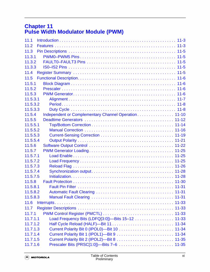
Chapter 11 Pulse Width Modulator Module (PWM)11.1 Introduction . . . . . . . . . . . . . . . . . . . . . . . . . . . . . . . . . . . . . . . . . . . . . . . . . . . 11-311.2 Features . . . . . . . . . . . . . . . . . . . . . . . . . . . . . . . . . . . . . . . . . . . . . . . . . . . . . 11-311.3 Pin Descriptions . . . . . . . . . . . . . . . . . . . . . . . . . . . . . . . . . . . . . . . . . . . . . . . 11-511.3.1 PWM0–PWM5 Pins . . . . . . . . . . . . . . . . . . . . . . . . . . . . . . . . . . . . . . . . . . 11-511.3.2 FAULT0–FAULT3 Pins . . . . . . . . . . . . . . . . . . . . . . . . . . . . . . . . . . . . . . . 11-511.3.3 IS0–IS2 Pins . . . . . . . . . . . . . . . . . . . . . . . . . . . . . . . . . . . . . . . . . . . . . . . 11-511.4 Register Summary . . . . . . . . . . . . . . . . . . . . . . . . . . . . . . . . . . . . . . . . . . . . . 11-511.5 Functional Description. . . . . . . . . . . . . . . . . . . . . . . . . . . . . . . . . . . . . . . . . . . 11-611.5.1 Block Diagram . . . . . . . . . . . . . . . . . . . . . . . . . . . . . . . . . . . . . . . . . . . . . . 11-611.5.2 Prescaler . . . . . . . . . . . . . . . . . . . . . . . . . . . . . . . . . . . . . . . . . . . . . . . . . . 11-611.5.3 PWM Generator. . . . . . . . . . . . . . . . . . . . . . . . . . . . . . . . . . . . . . . . . . . . . 11-611.5.3.1 Alignment . . . . . . . . . . . . . . . . . . . . . . . . . . . . . . . . . . . . . . . . . . . . . . . 11-711.5.3.2 Period . . . . . . . . . . . . . . . . . . . . . . . . . . . . . . . . . . . . . . . . . . . . . . . . . . 11-811.5.3.3 Duty Cycle . . . . . . . . . . . . . . . . . . . . . . . . . . . . . . . . . . . . . . . . . . . . . . 11-811.5.4 Independent or Complementary Channel Operation . . . . . . . . . . . . . . . . 11-1011.5.5 Deadtime Generators . . . . . . . . . . . . . . . . . . . . . . . . . . . . . . . . . . . . . . . 11-1211.5.5.1 Top/Bottom Correction . . . . . . . . . . . . . . . . . . . . . . . . . . . . . . . . . . . . 11-1411.5.5.2 Manual Correction . . . . . . . . . . . . . . . . . . . . . . . . . . . . . . . . . . . . . . . 11-1611.5.5.3 Current-Sensing Correction . . . . . . . . . . . . . . . . . . . . . . . . . . . . . . . . 11-1911.5.5.4 Output Polarity . . . . . . . . . . . . . . . . . . . . . . . . . . . . . . . . . . . . . . . . . . 11-2111.5.6 Software Output Control . . . . . . . . . . . . . . . . . . . . . . . . . . . . . . . . . . . . . 11-2211.5.7 PWM Generator Loading . . . . . . . . . . . . . . . . . . . . . . . . . . . . . . . . . . . . . 11-2511.5.7.1 Load Enable . . . . . . . . . . . . . . . . . . . . . . . . . . . . . . . . . . . . . . . . . . . . 11-2511.5.7.2 Load Frequency . . . . . . . . . . . . . . . . . . . . . . . . . . . . . . . . . . . . . . . . . 11-2511.5.7.3 Reload Flag . . . . . . . . . . . . . . . . . . . . . . . . . . . . . . . . . . . . . . . . . . . . 11-2611.5.7.4 Synchronization output . . . . . . . . . . . . . . . . . . . . . . . . . . . . . . . . . . . . 11-2811.5.7.5 Initialization. . . . . . . . . . . . . . . . . . . . . . . . . . . . . . . . . . . . . . . . . . . . . 11-2811.5.8 Fault Protection . . . . . . . . . . . . . . . . . . . . . . . . . . . . . . . . . . . . . . . . . . . . 11-3011.5.8.1 Fault Pin Filter . . . . . . . . . . . . . . . . . . . . . . . . . . . . . . . . . . . . . . . . . . 11-3111.5.8.2 Automatic Fault Clearing . . . . . . . . . . . . . . . . . . . . . . . . . . . . . . . . . . 11-3111.5.8.3 Manual Fault Clearing . . . . . . . . . . . . . . . . . . . . . . . . . . . . . . . . . . . . 11-3111.6 Interrupts . . . . . . . . . . . . . . . . . . . . . . . . . . . . . . . . . . . . . . . . . . . . . . . . . . . . 11-3311.7 Register Descriptions . . . . . . . . . . . . . . . . . . . . . . . . . . . . . . . . . . . . . . . . . . 11-3311.7.1 PWM Control Register (PMCTL) . . . . . . . . . . . . . . . . . . . . . . . . . . . . . . . 11-3311.7.1.1 Load Frequency Bits (LDFQ[3:0])—Bits 15–12 . . . . . . . . . . . . . . . . . 11-3311.7.1.2 Half Cycle Reload (HALF)—Bit 11 . . . . . . . . . . . . . . . . . . . . . . . . . . . 11-3411.7.1.3 Current Polarity Bit 0 (IPOL0)—Bit 10 . . . . . . . . . . . . . . . . . . . . . . . . 11-3411.7.1.4 Current Polarity Bit 1 (IPOL1)—Bit 9 . . . . . . . . . . . . . . . . . . . . . . . . . 11-3411.7.1.5 Current Polarity Bit 2 (IPOL2)—Bit 8 . . . . . . . . . . . . . . . . . . . . . . . . . 11-3511.7.1.6 Prescaler Bits (PRSC[1:0])—Bits 7–6 . . . . . . . . . . . . . . . . . . . . . . . . 11-35
xii DSP56F801/803/805/807 User’s Manual�Preliminary
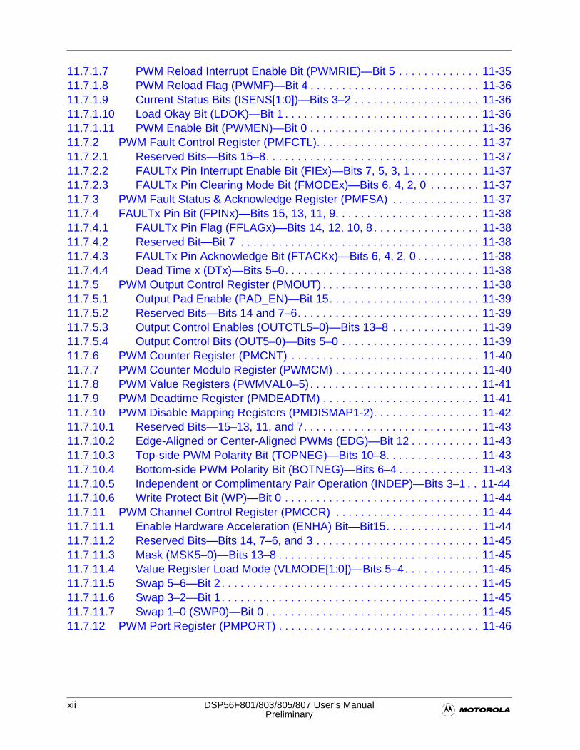
11.7.1.7 PWM Reload Interrupt Enable Bit (PWMRIE)—Bit 5 . . . . . . . . . . . . . 11-3511.7.1.8 PWM Reload Flag (PWMF)—Bit 4 . . . . . . . . . . . . . . . . . . . . . . . . . . . 11-3611.7.1.9 Current Status Bits (ISENS[1:0])—Bits 3–2 . . . . . . . . . . . . . . . . . . . . 11-3611.7.1.10 Load Okay Bit (LDOK)—Bit 1 . . . . . . . . . . . . . . . . . . . . . . . . . . . . . . . 11-3611.7.1.11 PWM Enable Bit (PWMEN)—Bit 0 . . . . . . . . . . . . . . . . . . . . . . . . . . . 11-3611.7.2 PWM Fault Control Register (PMFCTL). . . . . . . . . . . . . . . . . . . . . . . . . . 11-3711.7.2.1 Reserved Bits—Bits 15–8. . . . . . . . . . . . . . . . . . . . . . . . . . . . . . . . . . 11-3711.7.2.2 FAULTx Pin Interrupt Enable Bit (FIEx)—Bits 7, 5, 3, 1 . . . . . . . . . . . 11-3711.7.2.3 FAULTx Pin Clearing Mode Bit (FMODEx)—Bits 6, 4, 2, 0 . . . . . . . . 11-3711.7.3 PWM Fault Status & Acknowledge Register (PMFSA) . . . . . . . . . . . . . . 11-3711.7.4 FAULTx Pin Bit (FPINx)—Bits 15, 13, 11, 9. . . . . . . . . . . . . . . . . . . . . . . 11-3811.7.4.1 FAULTx Pin Flag (FFLAGx)—Bits 14, 12, 10, 8 . . . . . . . . . . . . . . . . . 11-3811.7.4.2 Reserved Bit—Bit 7 . . . . . . . . . . . . . . . . . . . . . . . . . . . . . . . . . . . . . . 11-3811.7.4.3 FAULTx Pin Acknowledge Bit (FTACKx)—Bits 6, 4, 2, 0 . . . . . . . . . . 11-3811.7.4.4 Dead Time x (DTx)—Bits 5–0. . . . . . . . . . . . . . . . . . . . . . . . . . . . . . . 11-3811.7.5 PWM Output Control Register (PMOUT) . . . . . . . . . . . . . . . . . . . . . . . . . 11-3811.7.5.1 Output Pad Enable (PAD_EN)—Bit 15. . . . . . . . . . . . . . . . . . . . . . . . 11-3911.7.5.2 Reserved Bits—Bits 14 and 7–6. . . . . . . . . . . . . . . . . . . . . . . . . . . . . 11-3911.7.5.3 Output Control Enables (OUTCTL5–0)—Bits 13–8 . . . . . . . . . . . . . . 11-3911.7.5.4 Output Control Bits (OUT5–0)—Bits 5–0 . . . . . . . . . . . . . . . . . . . . . . 11-3911.7.6 PWM Counter Register (PMCNT) . . . . . . . . . . . . . . . . . . . . . . . . . . . . . . 11-4011.7.7 PWM Counter Modulo Register (PWMCM) . . . . . . . . . . . . . . . . . . . . . . . 11-4011.7.8 PWM Value Registers (PWMVAL0–5). . . . . . . . . . . . . . . . . . . . . . . . . . . 11-4111.7.9 PWM Deadtime Register (PMDEADTM) . . . . . . . . . . . . . . . . . . . . . . . . . 11-4111.7.10 PWM Disable Mapping Registers (PMDISMAP1-2). . . . . . . . . . . . . . . . . 11-4211.7.10.1 Reserved Bits—15–13, 11, and 7. . . . . . . . . . . . . . . . . . . . . . . . . . . . 11-4311.7.10.2 Edge-Aligned or Center-Aligned PWMs (EDG)—Bit 12 . . . . . . . . . . . 11-4311.7.10.3 Top-side PWM Polarity Bit (TOPNEG)—Bits 10–8. . . . . . . . . . . . . . . 11-4311.7.10.4 Bottom-side PWM Polarity Bit (BOTNEG)—Bits 6–4 . . . . . . . . . . . . . 11-4311.7.10.5 Independent or Complimentary Pair Operation (INDEP)—Bits 3–1 . . 11-4411.7.10.6 Write Protect Bit (WP)—Bit 0 . . . . . . . . . . . . . . . . . . . . . . . . . . . . . . . 11-4411.7.11 PWM Channel Control Register (PMCCR) . . . . . . . . . . . . . . . . . . . . . . . 11-4411.7.11.1 Enable Hardware Acceleration (ENHA) Bit—Bit15. . . . . . . . . . . . . . . 11-4411.7.11.2 Reserved Bits—Bits 14, 7–6, and 3 . . . . . . . . . . . . . . . . . . . . . . . . . . 11-4511.7.11.3 Mask (MSK5–0)—Bits 13–8 . . . . . . . . . . . . . . . . . . . . . . . . . . . . . . . . 11-4511.7.11.4 Value Register Load Mode (VLMODE[1:0])—Bits 5–4. . . . . . . . . . . . 11-4511.7.11.5 Swap 5–6—Bit 2 . . . . . . . . . . . . . . . . . . . . . . . . . . . . . . . . . . . . . . . . . 11-4511.7.11.6 Swap 3–2—Bit 1 . . . . . . . . . . . . . . . . . . . . . . . . . . . . . . . . . . . . . . . . . 11-4511.7.11.7 Swap 1–0 (SWP0)—Bit 0 . . . . . . . . . . . . . . . . . . . . . . . . . . . . . . . . . . 11-4511.7.12 PWM Port Register (PMPORT) . . . . . . . . . . . . . . . . . . . . . . . . . . . . . . . . 11-46
�Table of Contents xiii
Preliminary
Chapter 12 Serial Communications Interface Module (SCI)12.1 Introduction . . . . . . . . . . . . . . . . . . . . . . . . . . . . . . . . . . . . . . . . . . . . . . . . . . . 12-312.2 Features . . . . . . . . . . . . . . . . . . . . . . . . . . . . . . . . . . . . . . . . . . . . . . . . . . . . . 12-312.3 Block Diagram. . . . . . . . . . . . . . . . . . . . . . . . . . . . . . . . . . . . . . . . . . . . . . . . . 12-412.4 External Pin Descriptions . . . . . . . . . . . . . . . . . . . . . . . . . . . . . . . . . . . . . . . . 12-412.4.1 TXD Pin . . . . . . . . . . . . . . . . . . . . . . . . . . . . . . . . . . . . . . . . . . . . . . . . . . . 12-412.4.2 RXD Pin . . . . . . . . . . . . . . . . . . . . . . . . . . . . . . . . . . . . . . . . . . . . . . . . . . . 12-412.5 Register Summary . . . . . . . . . . . . . . . . . . . . . . . . . . . . . . . . . . . . . . . . . . . . . 12-512.6 Definition of Terms . . . . . . . . . . . . . . . . . . . . . . . . . . . . . . . . . . . . . . . . . . . . . 12-512.7 Functional Description. . . . . . . . . . . . . . . . . . . . . . . . . . . . . . . . . . . . . . . . . . . 12-512.7.1 Data Frame Format . . . . . . . . . . . . . . . . . . . . . . . . . . . . . . . . . . . . . . . . . . 12-512.7.2 Baud Rate Generation . . . . . . . . . . . . . . . . . . . . . . . . . . . . . . . . . . . . . . . . 12-712.7.3 Block Diagram . . . . . . . . . . . . . . . . . . . . . . . . . . . . . . . . . . . . . . . . . . . . . . 12-812.7.3.1 Character Length . . . . . . . . . . . . . . . . . . . . . . . . . . . . . . . . . . . . . . . . . 12-812.7.3.2 Character Transmission . . . . . . . . . . . . . . . . . . . . . . . . . . . . . . . . . . . . 12-812.7.3.3 Break Characters . . . . . . . . . . . . . . . . . . . . . . . . . . . . . . . . . . . . . . . . 12-1012.7.3.4 Preambles . . . . . . . . . . . . . . . . . . . . . . . . . . . . . . . . . . . . . . . . . . . . . 12-1012.7.4 Receiver. . . . . . . . . . . . . . . . . . . . . . . . . . . . . . . . . . . . . . . . . . . . . . . . . . 12-1112.7.4.1 Character Length . . . . . . . . . . . . . . . . . . . . . . . . . . . . . . . . . . . . . . . . 12-1112.7.4.2 Character Reception . . . . . . . . . . . . . . . . . . . . . . . . . . . . . . . . . . . . . 12-1112.7.4.3 Data Sampling . . . . . . . . . . . . . . . . . . . . . . . . . . . . . . . . . . . . . . . . . . 12-1212.7.4.4 Framing Errors . . . . . . . . . . . . . . . . . . . . . . . . . . . . . . . . . . . . . . . . . . 12-1712.7.4.5 Baud Rate Tolerance . . . . . . . . . . . . . . . . . . . . . . . . . . . . . . . . . . . . . 12-1712.7.4.6 Receiver Wake-up . . . . . . . . . . . . . . . . . . . . . . . . . . . . . . . . . . . . . . . 12-2012.7.5 Single-Wire Operation . . . . . . . . . . . . . . . . . . . . . . . . . . . . . . . . . . . . . . . 12-2112.7.6 Loop Operation . . . . . . . . . . . . . . . . . . . . . . . . . . . . . . . . . . . . . . . . . . . . 12-2112.8 Register Descriptions . . . . . . . . . . . . . . . . . . . . . . . . . . . . . . . . . . . . . . . . . . 12-2212.8.1 SCI Baud Rate Register (SCIBR) . . . . . . . . . . . . . . . . . . . . . . . . . . . . . . 12-2212.8.1.1 Reserved Bits—Bits 15–13 . . . . . . . . . . . . . . . . . . . . . . . . . . . . . . . . 12-2212.8.1.2 SCI Baud Rate (SBR)—Bits 12–0 . . . . . . . . . . . . . . . . . . . . . . . . . . . 12-2212.8.2 SCI Control Register (SCICR) . . . . . . . . . . . . . . . . . . . . . . . . . . . . . . . . . 12-2212.8.2.1 Loop Select Bit (LOOP) - Bit 15 . . . . . . . . . . . . . . . . . . . . . . . . . . . . . 12-2312.8.2.2 Stop in Wait Mode Bit (SWAI)—Bit 14 . . . . . . . . . . . . . . . . . . . . . . . . 12-2312.8.2.3 Receiver Source Bit (RSRC)—Bit 13 . . . . . . . . . . . . . . . . . . . . . . . . . 12-2312.8.2.4 Data Format Mode Bit (M)—Bit 12 . . . . . . . . . . . . . . . . . . . . . . . . . . . 12-2312.8.2.5 Wake-up Condition Bit (WAKE)—Bit 11. . . . . . . . . . . . . . . . . . . . . . . 12-2412.8.2.6 Polarity Bit (POL)—Bit 10. . . . . . . . . . . . . . . . . . . . . . . . . . . . . . . . . . 12-2412.8.2.7 Parity Enable Bit (PE)—Bit 9 . . . . . . . . . . . . . . . . . . . . . . . . . . . . . . . 12-2412.8.2.8 Parity Type Bit (PT)—Bit 8 . . . . . . . . . . . . . . . . . . . . . . . . . . . . . . . . . 12-2412.8.2.9 Transmitter Empty Interrupt Enable Bit (TEIE)—Bit 7 . . . . . . . . . . . . 12-24
xiv DSP56F801/803/805/807 User’s Manual�Preliminary
12.8.2.10 Transmitter Idle Interrupt Enable Bit (TIIE)—Bit 6 . . . . . . . . . . . . . . . 12-2512.8.2.11 Receiver Full Interrupt Enable Bit (RIE)—Bit 5. . . . . . . . . . . . . . . . . . 12-2512.8.2.12 Receive Error Interrupt Enable Bit (REIE)—Bit 4 . . . . . . . . . . . . . . . . 12-2512.8.2.13 Transmitter Enable Bit (TE)—Bit 3 . . . . . . . . . . . . . . . . . . . . . . . . . . . 12-2512.8.2.14 Receiver Enable Bit (RE)—Bit 2 . . . . . . . . . . . . . . . . . . . . . . . . . . . . . 12-2512.8.2.15 Receiver Wake-up Bit (RWU)—Bit 1 . . . . . . . . . . . . . . . . . . . . . . . . . 12-2512.8.2.16 Send Break Bit (SBK)—Bit 0 . . . . . . . . . . . . . . . . . . . . . . . . . . . . . . . 12-2612.8.3 SCI Status Register (SCISR) . . . . . . . . . . . . . . . . . . . . . . . . . . . . . . . . . . 12-2612.8.3.1 Transmit Data Register Empty Flag (TDRE)—Bit 15 . . . . . . . . . . . . . 12-2612.8.3.2 Transmitter Idle Flag (TIDLE)—Bit 14 . . . . . . . . . . . . . . . . . . . . . . . . 12-2612.8.3.3 Receive Data Register Full Flag (RDRF)—Bit 13. . . . . . . . . . . . . . . . 12-2612.8.3.4 Receiver Idle Line Flag (RIDLE)—Bit 12 . . . . . . . . . . . . . . . . . . . . . . 12-2712.8.3.5 Overrun Flag (OR)—Bit 11 . . . . . . . . . . . . . . . . . . . . . . . . . . . . . . . . . 12-2712.8.3.6 Noise Flag (NF)—Bit 10 . . . . . . . . . . . . . . . . . . . . . . . . . . . . . . . . . . . 12-2712.8.3.7 Framing Error Flag (FE)—Bit 9. . . . . . . . . . . . . . . . . . . . . . . . . . . . . . 12-2712.8.3.8 Parity Error Flag (PF)—Bit 8. . . . . . . . . . . . . . . . . . . . . . . . . . . . . . . . 12-2812.8.3.9 Receiver Active Flag (RAF)—Bit 0 . . . . . . . . . . . . . . . . . . . . . . . . . . . 12-2812.8.4 SCI Data Register (SCIDR) . . . . . . . . . . . . . . . . . . . . . . . . . . . . . . . . . . . 12-2812.8.4.1 Reserved Bits—Bits 15–9. . . . . . . . . . . . . . . . . . . . . . . . . . . . . . . . . . 12-2812.8.4.2 Receive Data—Bits 8–0 . . . . . . . . . . . . . . . . . . . . . . . . . . . . . . . . . . . 12-2812.8.4.3 Transmit Data—Bits 8-0 . . . . . . . . . . . . . . . . . . . . . . . . . . . . . . . . . . . 12-2812.9 Low-Power Options . . . . . . . . . . . . . . . . . . . . . . . . . . . . . . . . . . . . . . . . . . . . 12-2912.9.1 Run Mode . . . . . . . . . . . . . . . . . . . . . . . . . . . . . . . . . . . . . . . . . . . . . . . . 12-2912.9.2 Wait Mode . . . . . . . . . . . . . . . . . . . . . . . . . . . . . . . . . . . . . . . . . . . . . . . . 12-2912.9.3 Stop Mode . . . . . . . . . . . . . . . . . . . . . . . . . . . . . . . . . . . . . . . . . . . . . . . . 12-2912.10 Interrupt Operation . . . . . . . . . . . . . . . . . . . . . . . . . . . . . . . . . . . . . . . . . . . . 12-3012.10.1 Interrupt Sources . . . . . . . . . . . . . . . . . . . . . . . . . . . . . . . . . . . . . . . . . . . 12-3012.10.1.1 Transmitter Interrupts . . . . . . . . . . . . . . . . . . . . . . . . . . . . . . . . . . . . . 12-3012.10.1.2 Receiver Interrupts . . . . . . . . . . . . . . . . . . . . . . . . . . . . . . . . . . . . . . . 12-3012.10.2 Recovery from Wait Mode . . . . . . . . . . . . . . . . . . . . . . . . . . . . . . . . . . . . 12-30
Chapter 13 Serial Peripheral Interface (SPI)13.1 Introduction . . . . . . . . . . . . . . . . . . . . . . . . . . . . . . . . . . . . . . . . . . . . . . . . . . . 13-313.2 Features . . . . . . . . . . . . . . . . . . . . . . . . . . . . . . . . . . . . . . . . . . . . . . . . . . . . . 13-313.3 Block Diagram . . . . . . . . . . . . . . . . . . . . . . . . . . . . . . . . . . . . . . . . . . . . . . . . . 13-413.4 Pin Descriptions . . . . . . . . . . . . . . . . . . . . . . . . . . . . . . . . . . . . . . . . . . . . . . . 13-413.4.1 MISO (Master In/Slave Out). . . . . . . . . . . . . . . . . . . . . . . . . . . . . . . . . . . . 13-413.4.2 MOSI (Master Out/Slave In). . . . . . . . . . . . . . . . . . . . . . . . . . . . . . . . . . . . 13-513.4.3 SCLK (Serial Clock) . . . . . . . . . . . . . . . . . . . . . . . . . . . . . . . . . . . . . . . . . . 13-513.4.4 SS (Slave Select) . . . . . . . . . . . . . . . . . . . . . . . . . . . . . . . . . . . . . . . . . . . . 13-513.5 Register Summary. . . . . . . . . . . . . . . . . . . . . . . . . . . . . . . . . . . . . . . . . . . . . . 13-6
�Table of Contents xv
Preliminary
13.6 Internal I/O Signals . . . . . . . . . . . . . . . . . . . . . . . . . . . . . . . . . . . . . . . . . . . . . 13-613.7 External I/O Signals . . . . . . . . . . . . . . . . . . . . . . . . . . . . . . . . . . . . . . . . . . . . 13-713.8 Functional Description. . . . . . . . . . . . . . . . . . . . . . . . . . . . . . . . . . . . . . . . . . . 13-813.8.1 Operating Modes . . . . . . . . . . . . . . . . . . . . . . . . . . . . . . . . . . . . . . . . . . . . 13-813.8.1.1 Master Mode . . . . . . . . . . . . . . . . . . . . . . . . . . . . . . . . . . . . . . . . . . . . 13-813.8.1.2 Slave Mode . . . . . . . . . . . . . . . . . . . . . . . . . . . . . . . . . . . . . . . . . . . . . 13-913.8.2 Transmission Formats . . . . . . . . . . . . . . . . . . . . . . . . . . . . . . . . . . . . . . . 13-1013.8.2.1 Data Transmission Length . . . . . . . . . . . . . . . . . . . . . . . . . . . . . . . . . 13-1013.8.2.2 Data Shift Ordering. . . . . . . . . . . . . . . . . . . . . . . . . . . . . . . . . . . . . . . 13-1013.8.2.3 Clock Phase and Polarity Controls. . . . . . . . . . . . . . . . . . . . . . . . . . . 13-1013.8.2.4 Transmission Format When CPHA = 0 . . . . . . . . . . . . . . . . . . . . . . . 13-1113.8.2.5 Transmission Format When CPHA = 1 . . . . . . . . . . . . . . . . . . . . . . . 13-1213.8.2.6 Transmission Initiation Latency . . . . . . . . . . . . . . . . . . . . . . . . . . . . . 13-1313.8.3 Transmission Data. . . . . . . . . . . . . . . . . . . . . . . . . . . . . . . . . . . . . . . . . . 13-1313.8.4 Error Conditions. . . . . . . . . . . . . . . . . . . . . . . . . . . . . . . . . . . . . . . . . . . . 13-1613.8.4.1 Overflow Error . . . . . . . . . . . . . . . . . . . . . . . . . . . . . . . . . . . . . . . . . . 13-1613.8.4.2 Mode Fault Error . . . . . . . . . . . . . . . . . . . . . . . . . . . . . . . . . . . . . . . . 13-1813.8.5 Interrupts . . . . . . . . . . . . . . . . . . . . . . . . . . . . . . . . . . . . . . . . . . . . . . . . . 13-2013.8.6 Resetting the SPI. . . . . . . . . . . . . . . . . . . . . . . . . . . . . . . . . . . . . . . . . . . 13-2113.9 Register Definitions . . . . . . . . . . . . . . . . . . . . . . . . . . . . . . . . . . . . . . . . . . . . 13-2213.9.1 SPI Status and Control Register (SPSCR) . . . . . . . . . . . . . . . . . . . . . . . 13-2213.9.1.1 Reserved Bit----Bit 15. . . . . . . . . . . . . . . . . . . . . . . . . . . . . . . . . . . . . 13-2313.9.1.2 Data Shift Order Bit (DSO)—Bit 14 . . . . . . . . . . . . . . . . . . . . . . . . . . 13-2313.9.1.3 SPI Receiver Full Bit (SPRF)—Bit 13. . . . . . . . . . . . . . . . . . . . . . . . . 13-2313.9.1.4 Error Interrupt Enable Bit (ERRIE)—Bit 12 . . . . . . . . . . . . . . . . . . . . 13-2313.9.1.5 Overflow Bit (OVRF)—Bit 11 . . . . . . . . . . . . . . . . . . . . . . . . . . . . . . . 13-2413.9.1.6 Mode Fault Bit (MODF)—Bit 10 . . . . . . . . . . . . . . . . . . . . . . . . . . . . . 13-2413.9.1.7 SPI Transmitter Empty Bit (SPTE)—Bit 9 . . . . . . . . . . . . . . . . . . . . . 13-2413.9.1.8 Mode Fault Enable Bit (MODFEN)—Bit 8 . . . . . . . . . . . . . . . . . . . . . 13-2413.9.1.9 SPI Baud Rate Select Bits (SPR1 and SPR0)—Bits 7,6 . . . . . . . . . . 13-2513.9.1.10 SPI Receiver Interrupt Enable Bit (SPRIE)—Bit 5 . . . . . . . . . . . . . . . 13-2513.9.1.11 SPI Master Bit (SPMSTR) — Bit 4 . . . . . . . . . . . . . . . . . . . . . . . . . . . 13-2513.9.1.12 Clock Polarity Bit (CPOL)—Bit 3 . . . . . . . . . . . . . . . . . . . . . . . . . . . . 13-2513.9.1.13 Clock Phase Bit (CPHA)—Bit 2 . . . . . . . . . . . . . . . . . . . . . . . . . . . . . 13-2613.9.1.14 SPI Enable (SPE)—Bit 1 . . . . . . . . . . . . . . . . . . . . . . . . . . . . . . . . . . 13-2613.9.1.15 SPI Transmit Interrupt Enable (SPTIE)—Bit 0 . . . . . . . . . . . . . . . . . . 13-2613.9.2 SPI Data Size Register (SPDSR) . . . . . . . . . . . . . . . . . . . . . . . . . . . . . . 13-2613.9.3 SPI Data Receive Register (SPDRR) . . . . . . . . . . . . . . . . . . . . . . . . . . . 13-2713.9.4 SPI Data Transmit Register (SPDTR) . . . . . . . . . . . . . . . . . . . . . . . . . . . 13-28
xvi DSP56F801/803/805/807 User’s Manual�Preliminary
Chapter 14 Quad Timer Module14.1 Introduction . . . . . . . . . . . . . . . . . . . . . . . . . . . . . . . . . . . . . . . . . . . . . . . . . . . 14-314.2 Features . . . . . . . . . . . . . . . . . . . . . . . . . . . . . . . . . . . . . . . . . . . . . . . . . . . . . 14-414.3 Pin Descriptions . . . . . . . . . . . . . . . . . . . . . . . . . . . . . . . . . . . . . . . . . . . . . . . 14-414.4 Register Summary. . . . . . . . . . . . . . . . . . . . . . . . . . . . . . . . . . . . . . . . . . . . . . 14-514.5 Functional Description. . . . . . . . . . . . . . . . . . . . . . . . . . . . . . . . . . . . . . . . . . . 14-514.5.1 Counting Options . . . . . . . . . . . . . . . . . . . . . . . . . . . . . . . . . . . . . . . . . . . . 14-514.5.2 External Inputs . . . . . . . . . . . . . . . . . . . . . . . . . . . . . . . . . . . . . . . . . . . . . . 14-614.5.3 OFLAG Output Signal . . . . . . . . . . . . . . . . . . . . . . . . . . . . . . . . . . . . . . . . 14-614.5.4 Master Signal . . . . . . . . . . . . . . . . . . . . . . . . . . . . . . . . . . . . . . . . . . . . . . . 14-614.6 Counting Mode Definitions . . . . . . . . . . . . . . . . . . . . . . . . . . . . . . . . . . . . . . . 14-614.6.1 Stop Mode . . . . . . . . . . . . . . . . . . . . . . . . . . . . . . . . . . . . . . . . . . . . . . . . . 14-614.6.2 Count Mode . . . . . . . . . . . . . . . . . . . . . . . . . . . . . . . . . . . . . . . . . . . . . . . . 14-614.6.3 Edge-Count Mode . . . . . . . . . . . . . . . . . . . . . . . . . . . . . . . . . . . . . . . . . . . 14-714.6.4 Gated-Count Mode . . . . . . . . . . . . . . . . . . . . . . . . . . . . . . . . . . . . . . . . . . 14-714.6.5 Quadrature-Count Mode . . . . . . . . . . . . . . . . . . . . . . . . . . . . . . . . . . . . . . 14-714.6.6 Signed-Count Mode . . . . . . . . . . . . . . . . . . . . . . . . . . . . . . . . . . . . . . . . . . 14-714.6.7 Triggered-Count Mode. . . . . . . . . . . . . . . . . . . . . . . . . . . . . . . . . . . . . . . . 14-814.6.8 One-Shot Mode . . . . . . . . . . . . . . . . . . . . . . . . . . . . . . . . . . . . . . . . . . . . . 14-814.6.9 Cascade-Count Mode . . . . . . . . . . . . . . . . . . . . . . . . . . . . . . . . . . . . . . . . 14-814.6.10 Pulse-Output Mode . . . . . . . . . . . . . . . . . . . . . . . . . . . . . . . . . . . . . . . . . . 14-914.6.11 Fixed-Frequency PWM Mode . . . . . . . . . . . . . . . . . . . . . . . . . . . . . . . . . . 14-914.6.12 Variable-Frequency PWM Mode . . . . . . . . . . . . . . . . . . . . . . . . . . . . . . . . 14-914.6.13 Usage of Compare Registers. . . . . . . . . . . . . . . . . . . . . . . . . . . . . . . . . . . 14-914.6.14 Usage of Capture Register . . . . . . . . . . . . . . . . . . . . . . . . . . . . . . . . . . . 14-1014.7 Register Definitions . . . . . . . . . . . . . . . . . . . . . . . . . . . . . . . . . . . . . . . . . . . . 14-1014.7.1 Control Registers (CTRL). . . . . . . . . . . . . . . . . . . . . . . . . . . . . . . . . . . . . 14-1114.7.1.1 Count Mode—Bits 15–13 . . . . . . . . . . . . . . . . . . . . . . . . . . . . . . . . . . 14-1114.7.1.2 Primary Count Source—Bits 12–9 . . . . . . . . . . . . . . . . . . . . . . . . . . . 14-1214.7.1.3 Secondary Count Source—Bits 8–7. . . . . . . . . . . . . . . . . . . . . . . . . . 14-1314.7.1.4 Count Once (ONCE)—Bit 6 . . . . . . . . . . . . . . . . . . . . . . . . . . . . . . . . 14-1314.7.1.5 Count Length (LENGTH)—Bit 5 . . . . . . . . . . . . . . . . . . . . . . . . . . . . . 14-1314.7.1.6 Count Direction (DIR)—Bit 4. . . . . . . . . . . . . . . . . . . . . . . . . . . . . . . . 14-1314.7.1.7 Co-channel Initialization (Co Init)—Bit 3 . . . . . . . . . . . . . . . . . . . . . . . 14-1314.7.1.8 Output Mode—Bits 2-0 . . . . . . . . . . . . . . . . . . . . . . . . . . . . . . . . . . . . 14-1414.7.2 Status and Control Registers (SCR) . . . . . . . . . . . . . . . . . . . . . . . . . . . . 14-1514.7.2.1 Timer Compare Flag (TCF)—Bit. . . . . . . . . . . . . . . . . . . . . . . . . . . . . 14-1514.7.2.2 Timer Compare Flag Interrupt Enable (TCFIE)—Bit 14 . . . . . . . . . . . 14-1514.7.2.3 Timer Overflow Flag (TOF)—Bit 13 . . . . . . . . . . . . . . . . . . . . . . . . . . 14-1514.7.2.4 Timer Overflow Flag Interrupt Enable (TOFIE)—Bit 12 . . . . . . . . . . . 14-1514.7.2.5 Input Edge Flag (IEF)—Bit 11 . . . . . . . . . . . . . . . . . . . . . . . . . . . . . . 14-16
�Table of Contents xvii
Preliminary
14.7.2.6 Input Edge Flag Interrupt Enable (IEFIE)—Bit 10 . . . . . . . . . . . . . . . 14-1614.7.2.7 Input Polarity Select (IPS)—Bit 9 . . . . . . . . . . . . . . . . . . . . . . . . . . . . 14-1614.7.2.8 External Input Signal (INPUT)—Bit 8 . . . . . . . . . . . . . . . . . . . . . . . . . 14-1614.7.2.9 Input Capture Mode (Capture Mode)—Bits 7–6. . . . . . . . . . . . . . . . . 14-1614.7.2.10 Master Mode (MSTR)—Bit 5 . . . . . . . . . . . . . . . . . . . . . . . . . . . . . . . 14-1614.7.2.11 Enable External OFLAG Force (EEOF)—Bit 4. . . . . . . . . . . . . . . . . . 14-1714.7.2.12 Forced OFLAG Value (VAL)—Bit 3 . . . . . . . . . . . . . . . . . . . . . . . . . . 14-1714.7.2.13 Force the OFLAG Output (FORCE)—Bit 2 . . . . . . . . . . . . . . . . . . . . 14-1714.7.2.14 Output Polarity Select (OPS)—Bit 1. . . . . . . . . . . . . . . . . . . . . . . . . . 14-1714.7.2.15 Output Enable (OEN)—Bit 0 . . . . . . . . . . . . . . . . . . . . . . . . . . . . . . . 14-1714.7.3 Compare Register #1 (CMP1) . . . . . . . . . . . . . . . . . . . . . . . . . . . . . . . . . 14-1714.7.4 Compare Register #2 (CMP2) . . . . . . . . . . . . . . . . . . . . . . . . . . . . . . . . . 14-1814.7.5 Capture Register (CAP). . . . . . . . . . . . . . . . . . . . . . . . . . . . . . . . . . . . . . 14-1914.7.6 Load Register (LOAD) . . . . . . . . . . . . . . . . . . . . . . . . . . . . . . . . . . . . . . . 14-1914.7.7 Hold Register (HOLD) . . . . . . . . . . . . . . . . . . . . . . . . . . . . . . . . . . . . . . . 14-2014.7.8 Counter Register (CNTR) . . . . . . . . . . . . . . . . . . . . . . . . . . . . . . . . . . . . 14-2114.8 Timer Group A, B, C, and D Functionality . . . . . . . . . . . . . . . . . . . . . . . . . . . 14-2114.8.1 Timer Group A (DSP56F803, DSP56F805, and DSP56F807 only) . . . . 14-2114.8.2 Timer Group B (DSP56F805 and DSP56F807 only) . . . . . . . . . . . . . . . . 14-2214.8.3 Timer Group C . . . . . . . . . . . . . . . . . . . . . . . . . . . . . . . . . . . . . . . . . . . . . 14-2214.8.3.1 DSP56F805 and DSP56F807 only. . . . . . . . . . . . . . . . . . . . . . . . . . . 14-2214.8.3.2 DSP56F801, DSP56F803, DSP56F805, and DSP56F807 . . . . . . . . 14-2314.8.4 Timer Group D . . . . . . . . . . . . . . . . . . . . . . . . . . . . . . . . . . . . . . . . . . . . . 14-2314.8.4.1 DSP56F801 . . . . . . . . . . . . . . . . . . . . . . . . . . . . . . . . . . . . . . . . . . . . 14-2314.8.4.2 DSP56F803 . . . . . . . . . . . . . . . . . . . . . . . . . . . . . . . . . . . . . . . . . . . . 14-2314.8.4.3 DSP56F805 and DSP56F807 . . . . . . . . . . . . . . . . . . . . . . . . . . . . . . 14-2314.8.4.4 General Input Behavior . . . . . . . . . . . . . . . . . . . . . . . . . . . . . . . . . . . 14-24
Chapter 15 On-chip Clock Synthesis (OCCS)15.1 Introduction . . . . . . . . . . . . . . . . . . . . . . . . . . . . . . . . . . . . . . . . . . . . . . . . . . . 15-315.2 Features . . . . . . . . . . . . . . . . . . . . . . . . . . . . . . . . . . . . . . . . . . . . . . . . . . . . . 15-315.3 Pin Descriptions . . . . . . . . . . . . . . . . . . . . . . . . . . . . . . . . . . . . . . . . . . . . . . . 15-315.3.1 Oscillator Inputs (XTAL, EXTAL) . . . . . . . . . . . . . . . . . . . . . . . . . . . . . . . . 15-315.3.2 External Crystal Design Considerations . . . . . . . . . . . . . . . . . . . . . . . . . . 15-315.3.2.1 Crystal Oscillator . . . . . . . . . . . . . . . . . . . . . . . . . . . . . . . . . . . . . . . . . 15-315.3.2.2 External Clock Source . . . . . . . . . . . . . . . . . . . . . . . . . . . . . . . . . . . . . 15-415.4 Register Summary . . . . . . . . . . . . . . . . . . . . . . . . . . . . . . . . . . . . . . . . . . . . . 15-515.5 Functional Description. . . . . . . . . . . . . . . . . . . . . . . . . . . . . . . . . . . . . . . . . . . 15-615.5.1 Timing . . . . . . . . . . . . . . . . . . . . . . . . . . . . . . . . . . . . . . . . . . . . . . . . . . . . 15-815.6 Register Definitions . . . . . . . . . . . . . . . . . . . . . . . . . . . . . . . . . . . . . . . . . . . . . 15-915.6.1 PLL Control Register (PLLCR) . . . . . . . . . . . . . . . . . . . . . . . . . . . . . . . . . 15-9
xviii DSP56F801/803/805/807 User’s Manual�Preliminary
15.6.1.1 PLL Interrupt Enable 1 (PLLIE1[1:0])—Bits 15–14. . . . . . . . . . . . . . . . 15-915.6.1.2 PLL Interrupt Enable 0 (PLLIE0[1:0])—Bits 13–12. . . . . . . . . . . . . . . . 15-915.6.1.3 Loss of Clock Interrupt Enable (LOCIE)—Bit 11. . . . . . . . . . . . . . . . . . 15-915.6.1.4 Reserved Bits—Bits 10–8. . . . . . . . . . . . . . . . . . . . . . . . . . . . . . . . . . 15-1015.6.1.5 Lock Detector On (LCKON)—Bit 7 . . . . . . . . . . . . . . . . . . . . . . . . . . . 15-1015.6.1.6 Charge Pump Tri-state (CHPMPTRI)—Bit 6 . . . . . . . . . . . . . . . . . . . 15-1015.6.1.7 Reserved Bit—Bit 5 . . . . . . . . . . . . . . . . . . . . . . . . . . . . . . . . . . . . . . 15-1015.6.1.8 PLL Power Down (PLLPD)—Bit 4 . . . . . . . . . . . . . . . . . . . . . . . . . . . 15-1015.6.1.9 Reserved Bit---Bit-3 . . . . . . . . . . . . . . . . . . . . . . . . . . . . . . . . . . . . . . 15-1015.6.1.10 Prescaler Clock Select (PRECS)—Bit 2 . . . . . . . . . . . . . . . . . . . . . . . 15-1015.6.1.11 ZCLOCK Source (ZSRC[1:0])—Bits 1–0 . . . . . . . . . . . . . . . . . . . . . . 15-1115.6.2 PLL Divide-By Register (PLLDB) . . . . . . . . . . . . . . . . . . . . . . . . . . . . . . . 15-1115.6.2.1 Reserved Bits—Bit 7 . . . . . . . . . . . . . . . . . . . . . . . . . . . . . . . . . . . . . 15-1115.6.2.2 PLL Clock Out Divide (PLLCOD[1:0])—Bits 11–10 . . . . . . . . . . . . . . 15-1115.6.2.3 PLL Clock In Divide (PLLCID[1:0])—Bits 9–8. . . . . . . . . . . . . . . . . . . 15-1215.6.2.4 PLL Divide-By (PLLDB[6:0])—Bits 6–0. . . . . . . . . . . . . . . . . . . . . . . . 15-1215.6.3 PLL Status Register (PLLSR) . . . . . . . . . . . . . . . . . . . . . . . . . . . . . . . . . 15-1215.6.3.1 PLL Loss of Lock Interrupt 1 (LOLI1)—Bit 15. . . . . . . . . . . . . . . . . . . 15-1215.6.3.2 PLL Loss of Lock Interrupt 0 (LOLI0)—Bit 14. . . . . . . . . . . . . . . . . . . 15-1315.6.3.3 Loss of Clock (LOCI)—Bit 13 . . . . . . . . . . . . . . . . . . . . . . . . . . . . . . . 15-1315.6.3.4 Reserved Bits—Bits 12–7 and 3. . . . . . . . . . . . . . . . . . . . . . . . . . . . . 15-1315.6.3.5 Loss of Lock 1 (LCK1)—Bit 6 . . . . . . . . . . . . . . . . . . . . . . . . . . . . . . . 15-1315.6.3.6 Loss of Lock 0 (LCK0)—Bit 5 . . . . . . . . . . . . . . . . . . . . . . . . . . . . . . . 15-1315.6.3.7 PLL Power Down (PLLPDN)—Bit 4 . . . . . . . . . . . . . . . . . . . . . . . . . . 15-1315.6.3.8 ZCLOCK Source (ZSRC[2:0])—Bits 2-0. . . . . . . . . . . . . . . . . . . . . . . 15-1315.6.4 Test Register (TESTR). . . . . . . . . . . . . . . . . . . . . . . . . . . . . . . . . . . . . . . 15-1415.6.4.1 Reserved Bits—Bits 15–8. . . . . . . . . . . . . . . . . . . . . . . . . . . . . . . . . . 15-1415.6.4.2 Test PLL Reference Clock (TPLLRef)—Bit 7 . . . . . . . . . . . . . . . . . . . 15-1415.6.4.3 Test PLL Clock (TFDBK)—Bit 6 . . . . . . . . . . . . . . . . . . . . . . . . . . . . . 15-1415.6.4.4 Test Feedback Clock (TFDBK)—Bit 5 . . . . . . . . . . . . . . . . . . . . . . . . 15-1415.6.4.5 Test Reference Frequency Clock (TFREF)—Bit 4 . . . . . . . . . . . . . . . 15-1415.6.4.6 Force Loss of Clock (FLOCI)—Bit 3 . . . . . . . . . . . . . . . . . . . . . . . . . . 15-1515.6.4.7 Force Loss of Lock 1 (FLOLI1)—Bit 2 . . . . . . . . . . . . . . . . . . . . . . . . 15-1515.6.4.8 Force Loss of Lock 0 (FLOLI0)—Bit 1 . . . . . . . . . . . . . . . . . . . . . . . . 15-1515.6.4.9 Test Mode (TM)—Bit 0 . . . . . . . . . . . . . . . . . . . . . . . . . . . . . . . . . . . . 15-1515.6.5 CLKO Select Register (CLKOSR) . . . . . . . . . . . . . . . . . . . . . . . . . . . . . . 15-1515.6.5.1 Reserved Bits—Bits 15–5. . . . . . . . . . . . . . . . . . . . . . . . . . . . . . . . . . 15-1615.6.5.2 CLKO Select (CLKOSEL)—Bits 4–0 . . . . . . . . . . . . . . . . . . . . . . . . . 15-1615.6.6 Internal Oscillator Control Register (IOSCTL) . . . . . . . . . . . . . . . . . . . . . 15-1615.6.6.1 ROPD - Relaxation Oscillator Power Down . . . . . . . . . . . . . . . . . . . . 15-1715.6.6.2 TRIM[7:0] - Internal Relaxation Oscillator TRIM bits . . . . . . . . . . . . . 15-1715.6.7 PLL Recommended Range of Operation. . . . . . . . . . . . . . . . . . . . . . . . . 15-1915.7 PLL Lock Time Specification . . . . . . . . . . . . . . . . . . . . . . . . . . . . . . . . . . . . . 15-20
�Table of Contents xix
Preliminary
15.7.1 Lock Time Definition . . . . . . . . . . . . . . . . . . . . . . . . . . . . . . . . . . . . . . . . 15-2015.7.2 Parametric Influences on Reaction Time. . . . . . . . . . . . . . . . . . . . . . . . . 15-2015.8 PLL Frequency Lock Detector Block. . . . . . . . . . . . . . . . . . . . . . . . . . . . . . . 15-20
Chapter 16 Reset, Low Voltage, Stop and Wait Operation16.1 Introduction . . . . . . . . . . . . . . . . . . . . . . . . . . . . . . . . . . . . . . . . . . . . . . . . . . . 16-316.2 Sources of Reset. . . . . . . . . . . . . . . . . . . . . . . . . . . . . . . . . . . . . . . . . . . . . . . 16-316.3 Register Summary . . . . . . . . . . . . . . . . . . . . . . . . . . . . . . . . . . . . . . . . . . . . . 16-416.4 Power-On-Reset and Low Voltage Interrupt . . . . . . . . . . . . . . . . . . . . . . . . . . 16-416.5 External Reset. . . . . . . . . . . . . . . . . . . . . . . . . . . . . . . . . . . . . . . . . . . . . . . . . 16-616.6 Computer Operating Properly (COP) Module . . . . . . . . . . . . . . . . . . . . . . . . . 16-716.6.1 COP Functional Description . . . . . . . . . . . . . . . . . . . . . . . . . . . . . . . . . . . 16-716.6.1.1 Time-out Specifications . . . . . . . . . . . . . . . . . . . . . . . . . . . . . . . . . . . . 16-716.6.1.2 COP after Reset . . . . . . . . . . . . . . . . . . . . . . . . . . . . . . . . . . . . . . . . . . 16-716.6.1.3 COP in Wait Mode . . . . . . . . . . . . . . . . . . . . . . . . . . . . . . . . . . . . . . . . 16-716.6.1.4 COP in Stop Mode . . . . . . . . . . . . . . . . . . . . . . . . . . . . . . . . . . . . . . . . 16-716.6.2 Register Definitions . . . . . . . . . . . . . . . . . . . . . . . . . . . . . . . . . . . . . . . . . . 16-816.6.2.1 COP Control Register (COPCTL). . . . . . . . . . . . . . . . . . . . . . . . . . . . . 16-816.6.2.2 COP Time-out Register (COPTO) . . . . . . . . . . . . . . . . . . . . . . . . . . . . 16-916.6.2.3 COP Service Register (COPSRV) . . . . . . . . . . . . . . . . . . . . . . . . . . . . 16-916.7 Stop and Wait Mode Disable Function . . . . . . . . . . . . . . . . . . . . . . . . . . . . . 16-1016.7.1 System Control Register (SYS_CNTL) . . . . . . . . . . . . . . . . . . . . . . . . . . 16-1116.7.1.1 Reserved Bits—Bits 15–12 and 7–5 . . . . . . . . . . . . . . . . . . . . . . . . . 16-1116.7.1.2 Timer I/O Pull-up Disable (TMR PD)—Bit 11 . . . . . . . . . . . . . . . . . . . 16-1116.7.1.3 Control Signal Pull-up Disable (CTRL PD)—Bit 10 . . . . . . . . . . . . . . 16-1116.7.1.4 Address Bus [5:0] Pull-up Disable (ADR PD)—Bit 9 . . . . . . . . . . . . . 16-1116.7.1.5 Data Bus I/O Pull-up Disable (DATA PD)—Bit 8 . . . . . . . . . . . . . . . . 16-1116.7.1.6 Bootmap (BOOTMAP_B)—Bit 4 . . . . . . . . . . . . . . . . . . . . . . . . . . . . 16-1116.7.1.7 2.7 V Low Voltage Interrupt Enable (LVIE27)—Bit 3 . . . . . . . . . . . . . 16-1216.7.1.8 2.2 V Low Voltage Interrupt Enable (LVIE22)—Bit 2 . . . . . . . . . . . . . 16-1216.7.1.9 Permanent STOP/WAIT Disable (PD)—Bit 1. . . . . . . . . . . . . . . . . . . 16-1216.7.1.10 Re-programmable STOP/WAIT Disable (RPD)—Bit 0. . . . . . . . . . . . 16-1216.7.2 System Status Register (SYS_STS) . . . . . . . . . . . . . . . . . . . . . . . . . . . . 16-1216.7.2.1 Reserved Bits—Bits 15–5 . . . . . . . . . . . . . . . . . . . . . . . . . . . . . . . . . 16-1316.7.2.2 COP Reset (COPR)—Bit 4. . . . . . . . . . . . . . . . . . . . . . . . . . . . . . . . . 16-1316.7.2.3 External Reset (EXTR)—Bit 3 . . . . . . . . . . . . . . . . . . . . . . . . . . . . . . 16-1316.7.2.4 Power on Reset (POR)—Bit 2 . . . . . . . . . . . . . . . . . . . . . . . . . . . . . . 16-1316.7.3 2.7 V Low Voltage Interrupt Source (LVIS27)—Bit 1. . . . . . . . . . . . . . . . 16-1316.7.4 2.2 Low Voltage Interrupt Source (LVIS 22)—Bit 0 . . . . . . . . . . . . . . . . . 16-1316.7.5 Most Significant Half of JTAG ID (MSH_ID) . . . . . . . . . . . . . . . . . . . . . . 16-1416.7.6 Least Significant Half of JTAG ID (LSH_ID) . . . . . . . . . . . . . . . . . . . . . . 16-14
xx DSP56F801/803/805/807 User’s Manual�Preliminary
16.7.7 Test Registers 0–4 (TST_REG0–TST_REG4) . . . . . . . . . . . . . . . . . . . . 16-1416.7.7.1 Operating Mode Register (OMR) . . . . . . . . . . . . . . . . . . . . . . . . . . . . 16-1416.7.7.2 Nested Looping (NL) Bit–15 . . . . . . . . . . . . . . . . . . . . . . . . . . . . . . . . 16-1516.7.7.3 Reserved Bits—Bits 14–9, 7 and 2. . . . . . . . . . . . . . . . . . . . . . . . . . . 16-1516.7.7.4 Condition Codes (CC)—Bit 8 . . . . . . . . . . . . . . . . . . . . . . . . . . . . . . . 16-1516.7.7.5 Stop Delay (SD)—Bit 6 . . . . . . . . . . . . . . . . . . . . . . . . . . . . . . . . . . . . 16-1616.7.7.6 Rounding (R)—Bit 5 . . . . . . . . . . . . . . . . . . . . . . . . . . . . . . . . . . . . . . 16-1616.7.7.7 Saturation (SA)—Bit 4 . . . . . . . . . . . . . . . . . . . . . . . . . . . . . . . . . . . . 16-1616.7.7.8 External X Memory (EX)—Bit 3 . . . . . . . . . . . . . . . . . . . . . . . . . . . . . 16-1716.7.7.9 Operating Mode B (MB)—Bit 1 . . . . . . . . . . . . . . . . . . . . . . . . . . . . . . 16-1716.7.7.10 Operating Mode A (MA)—Bit 0 . . . . . . . . . . . . . . . . . . . . . . . . . . . . . . 16-17
Chapter 17 OnCE Module17.1 Introduction . . . . . . . . . . . . . . . . . . . . . . . . . . . . . . . . . . . . . . . . . . . . . . . . . . . 17-317.2 Features . . . . . . . . . . . . . . . . . . . . . . . . . . . . . . . . . . . . . . . . . . . . . . . . . . . . . 17-317.3 Combined JTAG/OnCE Interface Overview . . . . . . . . . . . . . . . . . . . . . . . . . . 17-517.4 JTAG/OnCE Port Pin Descriptions . . . . . . . . . . . . . . . . . . . . . . . . . . . . . . . . . 17-617.5 Register Summary. . . . . . . . . . . . . . . . . . . . . . . . . . . . . . . . . . . . . . . . . . . . . . 17-717.6 OnCE Module Architecture . . . . . . . . . . . . . . . . . . . . . . . . . . . . . . . . . . . . . . . 17-717.7 Command, Status, and Control Registers . . . . . . . . . . . . . . . . . . . . . . . . . . . 17-1317.7.1 OnCE Shift Register (OSHR). . . . . . . . . . . . . . . . . . . . . . . . . . . . . . . . . . 17-1317.7.2 OnCE Command Register (OCMDR) . . . . . . . . . . . . . . . . . . . . . . . . . . . 17-1417.7.3 OnCE Decoder (ODEC). . . . . . . . . . . . . . . . . . . . . . . . . . . . . . . . . . . . . . 17-1617.7.4 OnCE Control Register (OCR). . . . . . . . . . . . . . . . . . . . . . . . . . . . . . . . . 17-1617.7.4.1 COP Timer Disable (COPDIS)—Bit 15. . . . . . . . . . . . . . . . . . . . . . . . 17-1617.7.4.2 Reserved Bit—Bit 14 . . . . . . . . . . . . . . . . . . . . . . . . . . . . . . . . . . . . . 17-1717.7.4.3 Breakpoint Configuration (BK[4:0])—Bits 13–9 . . . . . . . . . . . . . . . . . 17-1717.7.4.4 Reserved Bit—Bit 8 . . . . . . . . . . . . . . . . . . . . . . . . . . . . . . . . . . . . . . 17-1817.7.4.5 FIFO Halt (FH)—Bit 7 . . . . . . . . . . . . . . . . . . . . . . . . . . . . . . . . . . . . . 17-1817.7.4.6 Event Modifier (EM[1:0])—Bits 6–5 . . . . . . . . . . . . . . . . . . . . . . . . . . 17-1817.7.4.7 Power Down Mode (PWD)—Bit 4. . . . . . . . . . . . . . . . . . . . . . . . . . . . 17-2117.7.4.8 Breakpoint Selection (BS[1:0])—Bits 3–2. . . . . . . . . . . . . . . . . . . . . . 17-2117.7.4.9 Breakpoint Enable (BE[1:0])—Bits 1–0. . . . . . . . . . . . . . . . . . . . . . . . 17-2317.7.5 OnCE Breakpoint 2 Control Register (OBCTL2) . . . . . . . . . . . . . . . . . . . 17-2317.7.5.1 Reserved Bits—Bits 15–3. . . . . . . . . . . . . . . . . . . . . . . . . . . . . . . . . . 17-2417.7.5.2 Enable (EN)—Bit 2 . . . . . . . . . . . . . . . . . . . . . . . . . . . . . . . . . . . . . . . 17-2417.7.5.3 Invert (INV)—Bit 1 . . . . . . . . . . . . . . . . . . . . . . . . . . . . . . . . . . . . . . . 17-2417.7.5.4 Data/Address Select (DAT)—Bit 0 . . . . . . . . . . . . . . . . . . . . . . . . . . . 17-2417.7.6 OnCE Status Register (OSR). . . . . . . . . . . . . . . . . . . . . . . . . . . . . . . . . . 17-2417.7.6.1 Reserved Bits—Bits 7–5. . . . . . . . . . . . . . . . . . . . . . . . . . . . . . . . . . . 17-2417.7.6.2 OnCE Core Status (OS[1:0])—Bits 4–3 . . . . . . . . . . . . . . . . . . . . . . . 17-25
�Table of Contents xxi
Preliminary
17.7.6.3 Trace Occurrence (TO)—Bit 2 . . . . . . . . . . . . . . . . . . . . . . . . . . . . . . 17-2517.7.6.4 Hardware Breakpoint Occurrence (HBO)—Bit 1 . . . . . . . . . . . . . . . . 17-2517.7.6.5 Software Breakpoint Occurrence (SBO)—Bit 0 . . . . . . . . . . . . . . . . . 17-2517.8 Breakpoint and Trace Registers . . . . . . . . . . . . . . . . . . . . . . . . . . . . . . . . . . 17-2617.8.1 OnCE Breakpoint/Trace Counter Register (OCNTR) . . . . . . . . . . . . . . . 17-2617.8.2 OnCE Memory Address Latch Register (OMAL) . . . . . . . . . . . . . . . . . . . 17-2717.8.3 OnCE Breakpoint Address Register (OBAR). . . . . . . . . . . . . . . . . . . . . . 17-2717.8.4 OnCE Memory Address Comparator (OMAC). . . . . . . . . . . . . . . . . . . . . 17-2817.8.5 OnCE Breakpoint and Trace Section. . . . . . . . . . . . . . . . . . . . . . . . . . . . 17-2817.9 Pipeline Registers . . . . . . . . . . . . . . . . . . . . . . . . . . . . . . . . . . . . . . . . . . . . . 17-2917.9.1 OnCE PAB Fetch Register (OPABFR) . . . . . . . . . . . . . . . . . . . . . . . . . . 17-3017.9.2 OnCE PAB Decode Register (OPABDR) . . . . . . . . . . . . . . . . . . . . . . . . 17-3017.9.3 OnCE PAB Execute Register (OPABER) . . . . . . . . . . . . . . . . . . . . . . . . 17-3117.9.4 OnCE PAB Change-of-Flow FIFO (OPFIFO) . . . . . . . . . . . . . . . . . . . . . 17-3117.9.5 OnCE PDB Register (OPDBR) . . . . . . . . . . . . . . . . . . . . . . . . . . . . . . . . 17-3117.9.6 OnCE PGDB Register (OPGDBR) . . . . . . . . . . . . . . . . . . . . . . . . . . . . . 17-3317.9.7 OnCE FIFO History Buffer . . . . . . . . . . . . . . . . . . . . . . . . . . . . . . . . . . . . 17-3317.10 Breakpoint 2 Architecture . . . . . . . . . . . . . . . . . . . . . . . . . . . . . . . . . . . . . . . 17-3617.11 Breakpoint Configuration. . . . . . . . . . . . . . . . . . . . . . . . . . . . . . . . . . . . . . . . 17-3717.11.1 Programming the Breakpoints . . . . . . . . . . . . . . . . . . . . . . . . . . . . . . . . . 17-4117.11.2 . OnCE Trace Logic Operation . . . . . . . . . . . . . . . . . . . . . . . . . . . . . . . . 17-4217.12 The Debug Processing State . . . . . . . . . . . . . . . . . . . . . . . . . . . . . . . . . . . . 17-4317.12.1 OnCE Normal and Debug and STOP Modes . . . . . . . . . . . . . . . . . . . . . 17-4317.12.2 Entering Debug Mode . . . . . . . . . . . . . . . . . . . . . . . . . . . . . . . . . . . . . . . 17-4417.12.2.1 JTAG DEBUG_REQUEST . . . . . . . . . . . . . . . . . . . . . . . . . . . . . . . . . 17-4417.12.2.2 Software Request During Normal Activity . . . . . . . . . . . . . . . . . . . . . 17-4517.12.2.3 Trigger Events (Breakpoint/Trace Modes) . . . . . . . . . . . . . . . . . . . . . 17-4517.12.2.4 Re-entering Debug Mode with EX = 0 . . . . . . . . . . . . . . . . . . . . . . . . 17-4617.12.2.5 Exiting Debug Mode . . . . . . . . . . . . . . . . . . . . . . . . . . . . . . . . . . . . . . 17-4617.13 Accessing the OnCE Module . . . . . . . . . . . . . . . . . . . . . . . . . . . . . . . . . . . . 17-4617.13.1 Primitive JTAG Sequences . . . . . . . . . . . . . . . . . . . . . . . . . . . . . . . . . . . 17-4617.13.2 Entering the JTAG Test-Logic-Reset State . . . . . . . . . . . . . . . . . . . . . . . 17-4717.13.3 Loading the JTAG Instruction Register . . . . . . . . . . . . . . . . . . . . . . . . . . 17-4817.13.4 Accessing a JTAG Data Register . . . . . . . . . . . . . . . . . . . . . . . . . . . . . . 17-4917.13.4.1 JTAG/OnCE Interaction: Basic Sequences . . . . . . . . . . . . . . . . . . . . 17-5017.13.4.2 Executing a OnCE Command by Reading the OCR . . . . . . . . . . . . . 17-5117.13.4.3 Executing a OnCE Command by Writing the OCNTR . . . . . . . . . . . . 17-5317.13.4.4 OSR Status Polling. . . . . . . . . . . . . . . . . . . . . . . . . . . . . . . . . . . . . . . 17-5317.13.4.5 JTAGIR Status Polling . . . . . . . . . . . . . . . . . . . . . . . . . . . . . . . . . . . . 17-5417.13.4.6 DE Pin Polling . . . . . . . . . . . . . . . . . . . . . . . . . . . . . . . . . . . . . . . . . . 17-5517.13.5 OnCE Module Low Power Operation. . . . . . . . . . . . . . . . . . . . . . . . . . . . 17-5517.13.6 Resetting the Chip Without Resetting the OnCE Unit . . . . . . . . . . . . . . . 17-56
xxii DSP56F801/803/805/807 User’s Manual�Preliminary
Chapter 18 JTAG Port Introduction18.1 Introduction . . . . . . . . . . . . . . . . . . . . . . . . . . . . . . . . . . . . . . . . . . . . . . . . . . . 18-318.2 Features . . . . . . . . . . . . . . . . . . . . . . . . . . . . . . . . . . . . . . . . . . . . . . . . . . . . . 18-418.3 Pin Descriptions . . . . . . . . . . . . . . . . . . . . . . . . . . . . . . . . . . . . . . . . . . . . . . . 18-418.4 Register Summary. . . . . . . . . . . . . . . . . . . . . . . . . . . . . . . . . . . . . . . . . . . . . . 18-518.5 JTAG Port Architecture . . . . . . . . . . . . . . . . . . . . . . . . . . . . . . . . . . . . . . . . . . 18-518.5.1 JTAG Instruction Register (JTAGIR) and Decoder . . . . . . . . . . . . . . . . . . 18-618.5.1.1 EXTEST (B[3:0] = 0000). . . . . . . . . . . . . . . . . . . . . . . . . . . . . . . . . . . . 18-818.5.1.2 SAMPLE/PRELOAD (B[3:0] = 0001) . . . . . . . . . . . . . . . . . . . . . . . . . . 18-818.5.1.3 IDCODE (B[3:0] = 0010). . . . . . . . . . . . . . . . . . . . . . . . . . . . . . . . . . . . 18-918.5.1.4 EXTEST_PULLUP (B[3:0] = 0011). . . . . . . . . . . . . . . . . . . . . . . . . . . . 18-918.5.1.5 HIGHZ (B[3:0] = 0100) . . . . . . . . . . . . . . . . . . . . . . . . . . . . . . . . . . . . . 18-918.5.1.6 CLAMP (B[3:0] = 0101) . . . . . . . . . . . . . . . . . . . . . . . . . . . . . . . . . . . 18-1018.5.1.7 ENABLE_ONCE (B[3:0] = 0110) . . . . . . . . . . . . . . . . . . . . . . . . . . . . 18-1018.5.1.8 DEBUG_REQUEST (B[3:0] = 0111). . . . . . . . . . . . . . . . . . . . . . . . . . 18-1018.5.1.9 BYPASS (B[3:0] = 1111) . . . . . . . . . . . . . . . . . . . . . . . . . . . . . . . . . . 18-1018.5.2 JTAG Chip Identification (CID) Register . . . . . . . . . . . . . . . . . . . . . . . . . 18-1118.5.3 JTAG Boundary Scan Register (BSR) . . . . . . . . . . . . . . . . . . . . . . . . . . . 18-1218.5.4 JTAG Bypass Register (JTAGBR) . . . . . . . . . . . . . . . . . . . . . . . . . . . . . . 18-3218.6 TAP Controller . . . . . . . . . . . . . . . . . . . . . . . . . . . . . . . . . . . . . . . . . . . . . . . . 18-3318.7 DSP56F801/803/805/807 Restrictions . . . . . . . . . . . . . . . . . . . . . . . . . . . . . 18-35
Appendix A GlossaryA.1 Glossary . . . . . . . . . . . . . . . . . . . . . . . . . . . . . . . . . . . . . . . . . . . . . . . . . . . . . . A-3
Appendix B BSDL ListingB.1 DSP56F805 BSDL Listing - 144-Pin LQFP . . . . . . . . . . . . . . . . . . . . . . . . . . . . B-3
Appendix C Programmer’s SheetsC.1 Introduction . . . . . . . . . . . . . . . . . . . . . . . . . . . . . . . . . . . . . . . . . . . . . . . . . . . . C-3C.2 Instruction Set Summary . . . . . . . . . . . . . . . . . . . . . . . . . . . . . . . . . . . . . . . . . . C-3C.3 Interrupt, Vector, and Address Tables. . . . . . . . . . . . . . . . . . . . . . . . . . . . . . . C-11C.4 Programmer’s Sheets . . . . . . . . . . . . . . . . . . . . . . . . . . . . . . . . . . . . . . . . . . . C-12
�Table of Contents xxiii
Preliminary
Appendix D Packaging & Pinout InformationD.1 DSP56F801 Packaging & Pinout Information . . . . . . . . . . . . . . . . . . . . . . . . . . D-3D.2 DSP56F803 Packaging & Pinout Information . . . . . . . . . . . . . . . . . . . . . . . . . . D-6D.3 DSP56F805Package and Pin-Out Information . . . . . . . . . . . . . . . . . . . . . . . . . D-9D.4 Package and Pin-Out Information DSP56F807 . . . . . . . . . . . . . . . . . . . . . . . D-13

xxiv DSP56F801/803/805/807 User’s Manual�Preliminary
�List of Figures xxiii
Preliminary
LIST OF FIGURES
1-1 DSP56F801 Functional Block Diagram . . . . . . . . . . . . . . . . . . . . . . . . . . . 1-111-2 DSP56F803 Functional Block Diagram . . . . . . . . . . . . . . . . . . . . . . . . . . . 1-121-3 DSP56F805 Functional Block Diagram . . . . . . . . . . . . . . . . . . . . . . . . . . . 1-131-4 DSP56F807 Functional Block Diagram . . . . . . . . . . . . . . . . . . . . . . . . . . . 1-141-5 DSP56800 Core Block Diagram . . . . . . . . . . . . . . . . . . . . . . . . . . . . . . . . 1-181-6 DSP56800 Bus Block Diagram . . . . . . . . . . . . . . . . . . . . . . . . . . . . . . . . . 1-191-7 Register Programming Model for the DSP56800. . . . . . . . . . . . . . . . . . . . 1-372-1 DSP56F801 Signals Identified by Functional Group . . . . . . . . . . . . . . . . . . 2-42-2 DSP56F803 Signals Identified by Functional Group . . . . . . . . . . . . . . . . . . 2-52-3 DSP56F805 Signals Identified by Functional Group . . . . . . . . . . . . . . . . . . 2-62-4 DSP56F807 Signals Identified by Functional Group . . . . . . . . . . . . . . . . . . 2-72-5 DSP56F801 Power and Ground Pins . . . . . . . . . . . . . . . . . . . . . . . . . . . . . 2-92-6 DSP56F803 Power and Ground Pins . . . . . . . . . . . . . . . . . . . . . . . . . . . . . 2-92-7 DSP56F805 Power and Ground Pins . . . . . . . . . . . . . . . . . . . . . . . . . . . . 2-102-8 DSP56F807 Power and Ground Pins . . . . . . . . . . . . . . . . . . . . . . . . . . . . 2-103-3 DSP56F801/803/805/807 On-Board Address and Data Buses . . . . . . . . . 3-354-1 Interrupt Programming . . . . . . . . . . . . . . . . . . . . . . . . . . . . . . . . . . . . . . . . . 4-54-16 Test Interrupt Request Register 0 (TIRQ0) . . . . . . . . . . . . . . . . . . . . . . . . 4-134-17 Test Interrupt Request Register 1 (TIRQ1) . . . . . . . . . . . . . . . . . . . . . . . . 4-134-18 Test Interrupt Request Register 2 (TIRQ2) . . . . . . . . . . . . . . . . . . . . . . . . 4-134-19 Test Interrupt Request Register 3 (TIRQ3) . . . . . . . . . . . . . . . . . . . . . . . . 4-134-20 Test Interrupt Source Register 0 (TISR0) . . . . . . . . . . . . . . . . . . . . . . . . . 4-144-21 Test Interrupt Source Register 1 (TISR1) . . . . . . . . . . . . . . . . . . . . . . . . . 4-144-22 Test Interrupt Source Register 2 (TISR2) . . . . . . . . . . . . . . . . . . . . . . . . . 4-144-23 Test Interrupt Source Register 3 (TISR3) . . . . . . . . . . . . . . . . . . . . . . . . . 4-145-1 Flash Program Cycle . . . . . . . . . . . . . . . . . . . . . . . . . . . . . . . . . . . . . . . . . . 5-85-2 Flash Erase Cycle . . . . . . . . . . . . . . . . . . . . . . . . . . . . . . . . . . . . . . . . . . . . 5-85-3 Flash Mass Erase Cycle . . . . . . . . . . . . . . . . . . . . . . . . . . . . . . . . . . . . . . . 5-95-4 Program Flash Block Integration . . . . . . . . . . . . . . . . . . . . . . . . . . . . . . . . 5-105-5 Data Flash Block Integration . . . . . . . . . . . . . . . . . . . . . . . . . . . . . . . . . . . 5-115-6 Boot Flash Block Integration . . . . . . . . . . . . . . . . . . . . . . . . . . . . . . . . . . . 5-126-1 DSP56F803/805/807 Input/Output Block Diagram . . . . . . . . . . . . . . . . . . . 6-36-3 Bus Operation (Read/Write—Zero Wait States) . . . . . . . . . . . . . . . . . . . . . 6-66-4 Bus Operation (Read/Write—Four Wait States) . . . . . . . . . . . . . . . . . . . . . 6-67-1 Block Diagram Showing GPIO Connections for DSP56F803/805/807 . . . . 7-47-2 Bit-Slice View of the GPIO Logic . . . . . . . . . . . . . . . . . . . . . . . . . . . . . . . . . 7-5
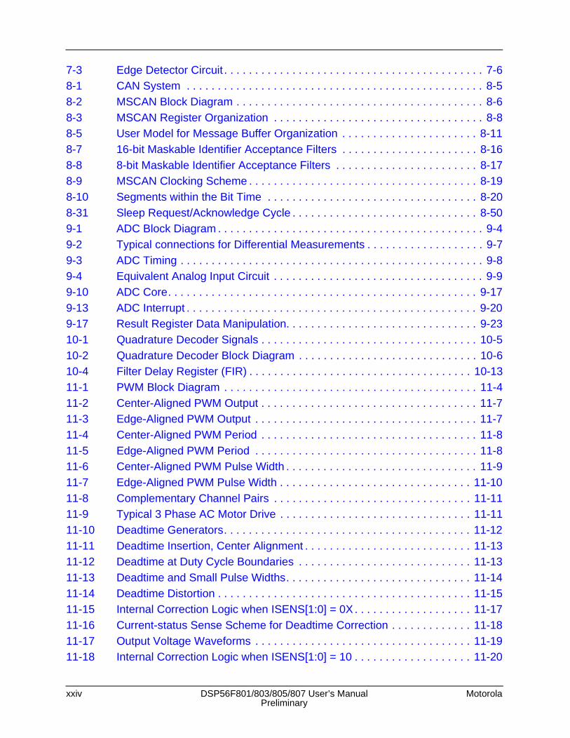
xxiv DSP56F801/803/805/807 User’s Manual MotorolaPreliminary
7-3 Edge Detector Circuit . . . . . . . . . . . . . . . . . . . . . . . . . . . . . . . . . . . . . . . . . . 7-68-1 CAN System . . . . . . . . . . . . . . . . . . . . . . . . . . . . . . . . . . . . . . . . . . . . . . . . 8-58-2 MSCAN Block Diagram . . . . . . . . . . . . . . . . . . . . . . . . . . . . . . . . . . . . . . . . 8-68-3 MSCAN Register Organization . . . . . . . . . . . . . . . . . . . . . . . . . . . . . . . . . . 8-88-5 User Model for Message Buffer Organization . . . . . . . . . . . . . . . . . . . . . . 8-118-7 16-bit Maskable Identifier Acceptance Filters . . . . . . . . . . . . . . . . . . . . . . 8-168-8 8-bit Maskable Identifier Acceptance Filters . . . . . . . . . . . . . . . . . . . . . . . 8-178-9 MSCAN Clocking Scheme . . . . . . . . . . . . . . . . . . . . . . . . . . . . . . . . . . . . . 8-198-10 Segments within the Bit Time . . . . . . . . . . . . . . . . . . . . . . . . . . . . . . . . . . 8-208-31 Sleep Request/Acknowledge Cycle . . . . . . . . . . . . . . . . . . . . . . . . . . . . . . 8-509-1 ADC Block Diagram . . . . . . . . . . . . . . . . . . . . . . . . . . . . . . . . . . . . . . . . . . . 9-49-2 Typical connections for Differential Measurements . . . . . . . . . . . . . . . . . . . 9-79-3 ADC Timing . . . . . . . . . . . . . . . . . . . . . . . . . . . . . . . . . . . . . . . . . . . . . . . . . 9-89-4 Equivalent Analog Input Circuit . . . . . . . . . . . . . . . . . . . . . . . . . . . . . . . . . . 9-99-10 ADC Core. . . . . . . . . . . . . . . . . . . . . . . . . . . . . . . . . . . . . . . . . . . . . . . . . . 9-179-13 ADC Interrupt . . . . . . . . . . . . . . . . . . . . . . . . . . . . . . . . . . . . . . . . . . . . . . . 9-209-17 Result Register Data Manipulation. . . . . . . . . . . . . . . . . . . . . . . . . . . . . . . 9-2310-1 Quadrature Decoder Signals . . . . . . . . . . . . . . . . . . . . . . . . . . . . . . . . . . . 10-510-2 Quadrature Decoder Block Diagram . . . . . . . . . . . . . . . . . . . . . . . . . . . . . 10-610-4 Filter Delay Register (FIR) . . . . . . . . . . . . . . . . . . . . . . . . . . . . . . . . . . . . 10-1311-1 PWM Block Diagram . . . . . . . . . . . . . . . . . . . . . . . . . . . . . . . . . . . . . . . . . 11-411-2 Center-Aligned PWM Output . . . . . . . . . . . . . . . . . . . . . . . . . . . . . . . . . . . 11-711-3 Edge-Aligned PWM Output . . . . . . . . . . . . . . . . . . . . . . . . . . . . . . . . . . . . 11-711-4 Center-Aligned PWM Period . . . . . . . . . . . . . . . . . . . . . . . . . . . . . . . . . . . 11-811-5 Edge-Aligned PWM Period . . . . . . . . . . . . . . . . . . . . . . . . . . . . . . . . . . . . 11-811-6 Center-Aligned PWM Pulse Width . . . . . . . . . . . . . . . . . . . . . . . . . . . . . . . 11-911-7 Edge-Aligned PWM Pulse Width . . . . . . . . . . . . . . . . . . . . . . . . . . . . . . . 11-1011-8 Complementary Channel Pairs . . . . . . . . . . . . . . . . . . . . . . . . . . . . . . . . 11-1111-9 Typical 3 Phase AC Motor Drive . . . . . . . . . . . . . . . . . . . . . . . . . . . . . . . 11-1111-10 Deadtime Generators. . . . . . . . . . . . . . . . . . . . . . . . . . . . . . . . . . . . . . . . 11-1211-11 Deadtime Insertion, Center Alignment . . . . . . . . . . . . . . . . . . . . . . . . . . . 11-1311-12 Deadtime at Duty Cycle Boundaries . . . . . . . . . . . . . . . . . . . . . . . . . . . . 11-1311-13 Deadtime and Small Pulse Widths. . . . . . . . . . . . . . . . . . . . . . . . . . . . . . 11-1411-14 Deadtime Distortion . . . . . . . . . . . . . . . . . . . . . . . . . . . . . . . . . . . . . . . . . 11-1511-15 Internal Correction Logic when ISENS[1:0] = 0X . . . . . . . . . . . . . . . . . . . 11-1711-16 Current-status Sense Scheme for Deadtime Correction . . . . . . . . . . . . . 11-1811-17 Output Voltage Waveforms . . . . . . . . . . . . . . . . . . . . . . . . . . . . . . . . . . . 11-1911-18 Internal Correction Logic when ISENS[1:0] = 10 . . . . . . . . . . . . . . . . . . . 11-20
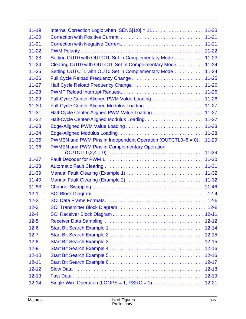
Motorola List of Figures xxvPreliminary
11-19 Internal Correction Logic when ISENS[1:0] = 11 . . . . . . . . . . . . . . . . . . . 11-2011-20 Correction with Positive Current . . . . . . . . . . . . . . . . . . . . . . . . . . . . . . . 11-2111-21 Correction with Negative Current. . . . . . . . . . . . . . . . . . . . . . . . . . . . . . . 11-2111-22 PWM Polarity . . . . . . . . . . . . . . . . . . . . . . . . . . . . . . . . . . . . . . . . . . . . . . 11-2211-23 Setting OUT0 with OUTCTL Set in Complementary Mode . . . . . . . . . . . 11-2311-24 Clearing OUT0 with OUTCTL Set In Complementary Mode . . . . . . . . . . 11-2411-25 Setting OUTCTL with OUT0 Set in Complementary Mode . . . . . . . . . . . 11-2411-26 Full Cycle Reload Frequency Change . . . . . . . . . . . . . . . . . . . . . . . . . . . 11-2511-27 Half Cycle Reload Frequency Change . . . . . . . . . . . . . . . . . . . . . . . . . . 11-2611-28 PWMF Reload Interrupt Request. . . . . . . . . . . . . . . . . . . . . . . . . . . . . . . 11-2611-29 Full-Cycle Center-Aligned PWM Value Loading . . . . . . . . . . . . . . . . . . . 11-2611-30 Full-Cycle Center-Aligned Modulus Loading . . . . . . . . . . . . . . . . . . . . . . 11-2711-31 Half-Cycle Center-Aligned PWM Value Loading . . . . . . . . . . . . . . . . . . . 11-2711-32 Half-Cycle Center-Aligned Modulus Loading. . . . . . . . . . . . . . . . . . . . . . 11-2711-33 Edge-Aligned PWM Value Loading . . . . . . . . . . . . . . . . . . . . . . . . . . . . . 11-2811-34 Edge-Aligned Modulus Loading. . . . . . . . . . . . . . . . . . . . . . . . . . . . . . . . 11-2811-35 PWMEN and PWM Pins in Independent Operation (OUTCTL0–5 = 0). . 11-2911-36 PWMEN and PWM Pins in Complementary Operation
(OUTCTL0,2,4 = 0) . . . . . . . . . . . . . . . . . . . . . . . . . . . . . . . . . . . . 11-2911-37 Fault Decoder for PWM 1 . . . . . . . . . . . . . . . . . . . . . . . . . . . . . . . . . . . . 11-3011-38 Automatic Fault Clearing . . . . . . . . . . . . . . . . . . . . . . . . . . . . . . . . . . . . . 11-3111-39 Manual Fault Clearing (Example 1) . . . . . . . . . . . . . . . . . . . . . . . . . . . . . 11-3211-40 Manual Fault Clearing (Example 2) . . . . . . . . . . . . . . . . . . . . . . . . . . . . . 11-3211-53 Channel Swapping. . . . . . . . . . . . . . . . . . . . . . . . . . . . . . . . . . . . . . . . . . 11-4612-1 SCI Block Diagram . . . . . . . . . . . . . . . . . . . . . . . . . . . . . . . . . . . . . . . . . . 12-412-2 SCI Data Frame Formats. . . . . . . . . . . . . . . . . . . . . . . . . . . . . . . . . . . . . . 12-612-3 SCI Transmitter Block Diagram . . . . . . . . . . . . . . . . . . . . . . . . . . . . . . . . . 12-812-4 SCI Receiver Block Diagram . . . . . . . . . . . . . . . . . . . . . . . . . . . . . . . . . . 12-1112-5 Receiver Data Sampling . . . . . . . . . . . . . . . . . . . . . . . . . . . . . . . . . . . . . 12-1212-6 Start Bit Search Example 1 . . . . . . . . . . . . . . . . . . . . . . . . . . . . . . . . . . . 12-1412-7 Start Bit Search Example 2 . . . . . . . . . . . . . . . . . . . . . . . . . . . . . . . . . . . 12-1512-8 Start Bit Search Example 3 . . . . . . . . . . . . . . . . . . . . . . . . . . . . . . . . . . . 12-1512-9 Start Bit Search Example 4 . . . . . . . . . . . . . . . . . . . . . . . . . . . . . . . . . . . 12-1612-10 Start Bit Search Example 5 . . . . . . . . . . . . . . . . . . . . . . . . . . . . . . . . . . . 12-1612-11 Start Bit Search Example 6 . . . . . . . . . . . . . . . . . . . . . . . . . . . . . . . . . . . 12-1712-12 Slow Data . . . . . . . . . . . . . . . . . . . . . . . . . . . . . . . . . . . . . . . . . . . . . . . . 12-1812-13 Fast Data . . . . . . . . . . . . . . . . . . . . . . . . . . . . . . . . . . . . . . . . . . . . . . . . . 12-1912-14 Single-Wire Operation (LOOPS = 1, RSRC = 1) . . . . . . . . . . . . . . . . . . . 12-21
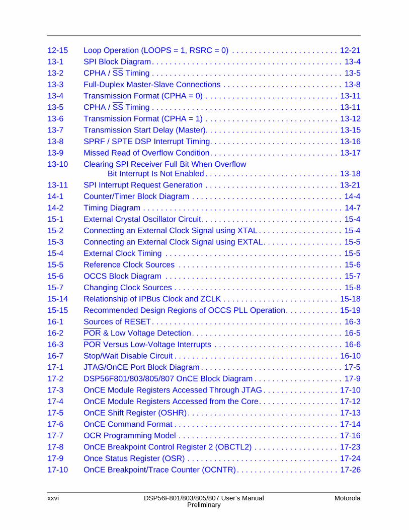
xxvi DSP56F801/803/805/807 User’s Manual MotorolaPreliminary
12-15 Loop Operation (LOOPS = 1, RSRC = 0) . . . . . . . . . . . . . . . . . . . . . . . . 12-2113-1 SPI Block Diagram. . . . . . . . . . . . . . . . . . . . . . . . . . . . . . . . . . . . . . . . . . . 13-413-2 CPHA / SS Timing . . . . . . . . . . . . . . . . . . . . . . . . . . . . . . . . . . . . . . . . . . . 13-513-3 Full-Duplex Master-Slave Connections . . . . . . . . . . . . . . . . . . . . . . . . . . . 13-813-4 Transmission Format (CPHA = 0) . . . . . . . . . . . . . . . . . . . . . . . . . . . . . . 13-1113-5 CPHA / SS Timing . . . . . . . . . . . . . . . . . . . . . . . . . . . . . . . . . . . . . . . . . . 13-1113-6 Transmission Format (CPHA = 1) . . . . . . . . . . . . . . . . . . . . . . . . . . . . . . 13-1213-7 Transmission Start Delay (Master). . . . . . . . . . . . . . . . . . . . . . . . . . . . . . 13-1513-8 SPRF / SPTE DSP Interrupt Timing. . . . . . . . . . . . . . . . . . . . . . . . . . . . . 13-1613-9 Missed Read of Overflow Condition. . . . . . . . . . . . . . . . . . . . . . . . . . . . . 13-1713-10 Clearing SPI Receiver Full Bit When Overflow
Bit Interrupt Is Not Enabled . . . . . . . . . . . . . . . . . . . . . . . . . . . . . . 13-1813-11 SPI Interrupt Request Generation . . . . . . . . . . . . . . . . . . . . . . . . . . . . . . 13-2114-1 Counter/Timer Block Diagram . . . . . . . . . . . . . . . . . . . . . . . . . . . . . . . . . . 14-414-2 Timing Diagram . . . . . . . . . . . . . . . . . . . . . . . . . . . . . . . . . . . . . . . . . . . . . 14-715-1 External Crystal Oscillator Circuit. . . . . . . . . . . . . . . . . . . . . . . . . . . . . . . . 15-415-2 Connecting an External Clock Signal using XTAL . . . . . . . . . . . . . . . . . . . 15-415-3 Connecting an External Clock Signal using EXTAL. . . . . . . . . . . . . . . . . . 15-515-4 External Clock Timing . . . . . . . . . . . . . . . . . . . . . . . . . . . . . . . . . . . . . . . . 15-515-5 Reference Clock Sources . . . . . . . . . . . . . . . . . . . . . . . . . . . . . . . . . . . . . 15-615-6 OCCS Block Diagram . . . . . . . . . . . . . . . . . . . . . . . . . . . . . . . . . . . . . . . . 15-715-7 Changing Clock Sources . . . . . . . . . . . . . . . . . . . . . . . . . . . . . . . . . . . . . . 15-815-14 Relationship of IPBus Clock and ZCLK . . . . . . . . . . . . . . . . . . . . . . . . . . 15-1815-15 Recommended Design Regions of OCCS PLL Operation. . . . . . . . . . . . 15-1916-1 Sources of RESET. . . . . . . . . . . . . . . . . . . . . . . . . . . . . . . . . . . . . . . . . . . 16-316-2 POR & Low Voltage Detection. . . . . . . . . . . . . . . . . . . . . . . . . . . . . . . . . . 16-516-3 POR Versus Low-Voltage Interrupts . . . . . . . . . . . . . . . . . . . . . . . . . . . . . 16-616-7 Stop/Wait Disable Circuit . . . . . . . . . . . . . . . . . . . . . . . . . . . . . . . . . . . . . 16-1017-1 JTAG/OnCE Port Block Diagram . . . . . . . . . . . . . . . . . . . . . . . . . . . . . . . . 17-517-2 DSP56F801/803/805/807 OnCE Block Diagram . . . . . . . . . . . . . . . . . . . . 17-917-3 OnCE Module Registers Accessed Through JTAG . . . . . . . . . . . . . . . . . 17-1017-4 OnCE Module Registers Accessed from the Core. . . . . . . . . . . . . . . . . . 17-1217-5 OnCE Shift Register (OSHR). . . . . . . . . . . . . . . . . . . . . . . . . . . . . . . . . . 17-1317-6 OnCE Command Format . . . . . . . . . . . . . . . . . . . . . . . . . . . . . . . . . . . . . 17-1417-7 OCR Programming Model . . . . . . . . . . . . . . . . . . . . . . . . . . . . . . . . . . . . 17-1617-8 OnCE Breakpoint Control Register 2 (OBCTL2) . . . . . . . . . . . . . . . . . . . 17-2317-9 Once Status Register (OSR) . . . . . . . . . . . . . . . . . . . . . . . . . . . . . . . . . . 17-2417-10 OnCE Breakpoint/Trace Counter (OCNTR). . . . . . . . . . . . . . . . . . . . . . . 17-26
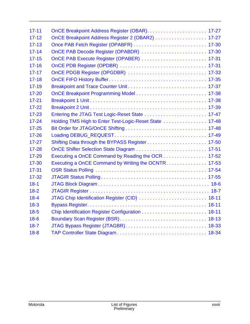
Motorola List of Figures xxviiPreliminary
17-11 OnCE Breakpoint Address Register (OBAR). . . . . . . . . . . . . . . . . . . . . . 17-2717-12 OnCE Breakpoint Address Register 2 (OBAR2) . . . . . . . . . . . . . . . . . . . 17-2717-13 Once PAB Fetch Register (OPABFR) . . . . . . . . . . . . . . . . . . . . . . . . . . . 17-3017-14 OnCE PAB Decode Register (OPABDR) . . . . . . . . . . . . . . . . . . . . . . . . 17-3017-15 OnCE PAB Execute Register (OPABER) . . . . . . . . . . . . . . . . . . . . . . . . 17-3117-16 OnCE PDB Register (OPDBR) . . . . . . . . . . . . . . . . . . . . . . . . . . . . . . . . 17-3117-17 OnCE PDGB Register (OPGDBR) . . . . . . . . . . . . . . . . . . . . . . . . . . . . . 17-3317-18 OnCE FIFO History Buffer . . . . . . . . . . . . . . . . . . . . . . . . . . . . . . . . . . . . 17-3517-19 Breakpoint and Trace Counter Unit . . . . . . . . . . . . . . . . . . . . . . . . . . . . . 17-3717-20 OnCE Breakpoint Programming Model . . . . . . . . . . . . . . . . . . . . . . . . . . 17-3817-21 Breakpoint 1 Unit . . . . . . . . . . . . . . . . . . . . . . . . . . . . . . . . . . . . . . . . . . . 17-3817-22 Breakpoint 2 Unit . . . . . . . . . . . . . . . . . . . . . . . . . . . . . . . . . . . . . . . . . . . 17-3917-23 Entering the JTAG Test Logic-Reset State . . . . . . . . . . . . . . . . . . . . . . . 17-4717-24 Holding TMS High to Enter Test-Logic-Reset State . . . . . . . . . . . . . . . . 17-4817-25 Bit Order for JTAG/OnCE Shifting . . . . . . . . . . . . . . . . . . . . . . . . . . . . . . 17-4817-26 Loading DEBUG_REQUEST. . . . . . . . . . . . . . . . . . . . . . . . . . . . . . . . . . 17-4917-27 Shifting Data through the BYPASS Register . . . . . . . . . . . . . . . . . . . . . . 17-5017-28 OnCE Shifter Selection State Diagram . . . . . . . . . . . . . . . . . . . . . . . . . . 17-5117-29 Executing a OnCE Command by Reading the OCR . . . . . . . . . . . . . . . . 17-5217-30 Executing a OnCE Command by Writing the OCNTR. . . . . . . . . . . . . . . 17-5317-31 OSR Status Polling . . . . . . . . . . . . . . . . . . . . . . . . . . . . . . . . . . . . . . . . . 17-5417-32 JTAGIR Status Polling . . . . . . . . . . . . . . . . . . . . . . . . . . . . . . . . . . . . . . . 17-5518-1 JTAG Block Diagram . . . . . . . . . . . . . . . . . . . . . . . . . . . . . . . . . . . . . . . . . 18-618-2 JTAGIR Register . . . . . . . . . . . . . . . . . . . . . . . . . . . . . . . . . . . . . . . . . . . . 18-718-4 JTAG Chip Identification Register (CID) . . . . . . . . . . . . . . . . . . . . . . . . . 18-1118-3 Bypass Register. . . . . . . . . . . . . . . . . . . . . . . . . . . . . . . . . . . . . . . . . . . . 18-1118-5 Chip Identification Register Configuration . . . . . . . . . . . . . . . . . . . . . . . . 18-1118-6 Boundary Scan Register (BSR) . . . . . . . . . . . . . . . . . . . . . . . . . . . . . . . . 18-1318-7 JTAG Bypass Register (JTAGBR). . . . . . . . . . . . . . . . . . . . . . . . . . . . . . 18-3318-8 TAP Controller State Diagram . . . . . . . . . . . . . . . . . . . . . . . . . . . . . . . . . 18-34

xxviii DSP56F801/803/805/807 User’s Manual MotorolaPreliminary
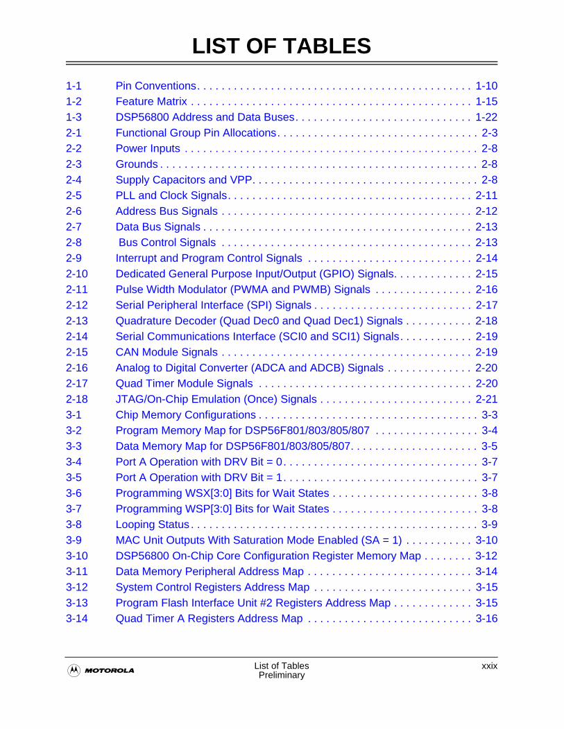
�List of Tables xxixPreliminary
LIST OF TABLES
1-1 Pin Conventions. . . . . . . . . . . . . . . . . . . . . . . . . . . . . . . . . . . . . . . . . . . . . 1-101-2 Feature Matrix . . . . . . . . . . . . . . . . . . . . . . . . . . . . . . . . . . . . . . . . . . . . . . 1-151-3 DSP56800 Address and Data Buses. . . . . . . . . . . . . . . . . . . . . . . . . . . . . 1-222-1 Functional Group Pin Allocations. . . . . . . . . . . . . . . . . . . . . . . . . . . . . . . . . 2-32-2 Power Inputs . . . . . . . . . . . . . . . . . . . . . . . . . . . . . . . . . . . . . . . . . . . . . . . . 2-82-3 Grounds . . . . . . . . . . . . . . . . . . . . . . . . . . . . . . . . . . . . . . . . . . . . . . . . . . . . 2-82-4 Supply Capacitors and VPP. . . . . . . . . . . . . . . . . . . . . . . . . . . . . . . . . . . . . 2-82-5 PLL and Clock Signals. . . . . . . . . . . . . . . . . . . . . . . . . . . . . . . . . . . . . . . . 2-112-6 Address Bus Signals . . . . . . . . . . . . . . . . . . . . . . . . . . . . . . . . . . . . . . . . . 2-122-7 Data Bus Signals . . . . . . . . . . . . . . . . . . . . . . . . . . . . . . . . . . . . . . . . . . . . 2-132-8 Bus Control Signals . . . . . . . . . . . . . . . . . . . . . . . . . . . . . . . . . . . . . . . . . 2-132-9 Interrupt and Program Control Signals . . . . . . . . . . . . . . . . . . . . . . . . . . . 2-142-10 Dedicated General Purpose Input/Output (GPIO) Signals. . . . . . . . . . . . . 2-152-11 Pulse Width Modulator (PWMA and PWMB) Signals . . . . . . . . . . . . . . . . 2-162-12 Serial Peripheral Interface (SPI) Signals . . . . . . . . . . . . . . . . . . . . . . . . . . 2-172-13 Quadrature Decoder (Quad Dec0 and Quad Dec1) Signals . . . . . . . . . . . 2-182-14 Serial Communications Interface (SCI0 and SCI1) Signals. . . . . . . . . . . . 2-192-15 CAN Module Signals . . . . . . . . . . . . . . . . . . . . . . . . . . . . . . . . . . . . . . . . . 2-192-16 Analog to Digital Converter (ADCA and ADCB) Signals . . . . . . . . . . . . . . 2-202-17 Quad Timer Module Signals . . . . . . . . . . . . . . . . . . . . . . . . . . . . . . . . . . . 2-202-18 JTAG/On-Chip Emulation (Once) Signals . . . . . . . . . . . . . . . . . . . . . . . . . 2-213-1 Chip Memory Configurations . . . . . . . . . . . . . . . . . . . . . . . . . . . . . . . . . . . . 3-33-2 Program Memory Map for DSP56F801/803/805/807 . . . . . . . . . . . . . . . . . 3-43-3 Data Memory Map for DSP56F801/803/805/807. . . . . . . . . . . . . . . . . . . . . 3-53-4 Port A Operation with DRV Bit = 0. . . . . . . . . . . . . . . . . . . . . . . . . . . . . . . . 3-73-5 Port A Operation with DRV Bit = 1. . . . . . . . . . . . . . . . . . . . . . . . . . . . . . . . 3-73-6 Programming WSX[3:0] Bits for Wait States . . . . . . . . . . . . . . . . . . . . . . . . 3-83-7 Programming WSP[3:0] Bits for Wait States . . . . . . . . . . . . . . . . . . . . . . . . 3-83-8 Looping Status . . . . . . . . . . . . . . . . . . . . . . . . . . . . . . . . . . . . . . . . . . . . . . . 3-93-9 MAC Unit Outputs With Saturation Mode Enabled (SA = 1) . . . . . . . . . . . 3-103-10 DSP56800 On-Chip Core Configuration Register Memory Map . . . . . . . . 3-123-11 Data Memory Peripheral Address Map . . . . . . . . . . . . . . . . . . . . . . . . . . . 3-143-12 System Control Registers Address Map . . . . . . . . . . . . . . . . . . . . . . . . . . 3-153-13 Program Flash Interface Unit #2 Registers Address Map . . . . . . . . . . . . . 3-153-14 Quad Timer A Registers Address Map . . . . . . . . . . . . . . . . . . . . . . . . . . . 3-16
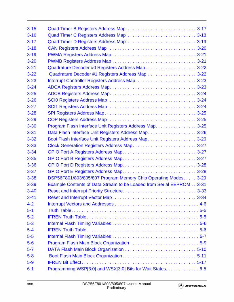
xxx DSP56F801/803/805/807 User’s Manual�Preliminary
3-15 Quad Timer B Registers Address Map . . . . . . . . . . . . . . . . . . . . . . . . . . . 3-173-16 Quad Timer C Registers Address Map . . . . . . . . . . . . . . . . . . . . . . . . . . . 3-183-17 Quad Timer D Registers Address Map . . . . . . . . . . . . . . . . . . . . . . . . . . . 3-193-18 CAN Registers Address Map . . . . . . . . . . . . . . . . . . . . . . . . . . . . . . . . . . . 3-203-19 PWMA Registers Address Map . . . . . . . . . . . . . . . . . . . . . . . . . . . . . . . . . 3-213-20 PWMB Registers Address Map . . . . . . . . . . . . . . . . . . . . . . . . . . . . . . . . . 3-213-21 Quadrature Decoder #0 Registers Address Map. . . . . . . . . . . . . . . . . . . . 3-223-22 Quadrature Decoder #1 Registers Address Map . . . . . . . . . . . . . . . . . . . 3-223-23 Interrupt Controller Registers Address Map. . . . . . . . . . . . . . . . . . . . . . . . 3-233-24 ADCA Registers Address Map. . . . . . . . . . . . . . . . . . . . . . . . . . . . . . . . . . 3-233-25 ADCB Registers Address Map. . . . . . . . . . . . . . . . . . . . . . . . . . . . . . . . . . 3-243-26 SCI0 Registers Address Map. . . . . . . . . . . . . . . . . . . . . . . . . . . . . . . . . . . 3-243-27 SCI1 Registers Address Map. . . . . . . . . . . . . . . . . . . . . . . . . . . . . . . . . . . 3-243-28 SPI Registers Address Map. . . . . . . . . . . . . . . . . . . . . . . . . . . . . . . . . . . . 3-253-29 COP Registers Address Map. . . . . . . . . . . . . . . . . . . . . . . . . . . . . . . . . . . 3-253-30 Program Flash Interface Unit Registers Address Map. . . . . . . . . . . . . . . . 3-253-31 Data Flash Interface Unit Registers Address Map. . . . . . . . . . . . . . . . . . . 3-263-32 Boot Flash Interface Unit Registers Address Map . . . . . . . . . . . . . . . . . . . 3-263-33 Clock Generation Registers Address Map. . . . . . . . . . . . . . . . . . . . . . . . . 3-273-34 GPIO Port A Registers Address Map. . . . . . . . . . . . . . . . . . . . . . . . . . . . . 3-273-35 GPIO Port B Registers Address Map. . . . . . . . . . . . . . . . . . . . . . . . . . . . . 3-273-36 GPIO Port D Registers Address Map. . . . . . . . . . . . . . . . . . . . . . . . . . . . . 3-283-37 GPIO Port E Registers Address Map. . . . . . . . . . . . . . . . . . . . . . . . . . . . . 3-283-38 DSP56F801/803/805/807 Program Memory Chip Operating Modes. . . . . 3-293-39 Example Contents of Data Stream to be Loaded from Serial EEPROM . . 3-313-40 Reset and Interrupt Priority Structure. . . . . . . . . . . . . . . . . . . . . . . . . . . . . 3-333-41 Reset and Interrupt Vector Map. . . . . . . . . . . . . . . . . . . . . . . . . . . . . . . . . 3-344-2 Interrupt Vectors and Addresses . . . . . . . . . . . . . . . . . . . . . . . . . . . . . . . . . 4-65-1 Truth Table. . . . . . . . . . . . . . . . . . . . . . . . . . . . . . . . . . . . . . . . . . . . . . . . . . 5-55-2 IFREN Truth Table. . . . . . . . . . . . . . . . . . . . . . . . . . . . . . . . . . . . . . . . . . . . 5-55-3 Internal Flash Timing Variables . . . . . . . . . . . . . . . . . . . . . . . . . . . . . . . . . . 5-65-4 IFREN Truth Table. . . . . . . . . . . . . . . . . . . . . . . . . . . . . . . . . . . . . . . . . . . . 5-65-5 Internal Flash Timing Variables . . . . . . . . . . . . . . . . . . . . . . . . . . . . . . . . . . 5-75-6 Program Flash Main Block Organization . . . . . . . . . . . . . . . . . . . . . . . . . . . 5-95-7 DATA Flash Main Block Organization . . . . . . . . . . . . . . . . . . . . . . . . . . . . 5-105-8 Boot Flash Main Block Organization. . . . . . . . . . . . . . . . . . . . . . . . . . . . . 5-115-9 IFREN Bit Effect . . . . . . . . . . . . . . . . . . . . . . . . . . . . . . . . . . . . . . . . . . . . . 5-176-1 Programming WSP[3:0] and WSX[3:0] Bits for Wait States. . . . . . . . . . . . . 6-5
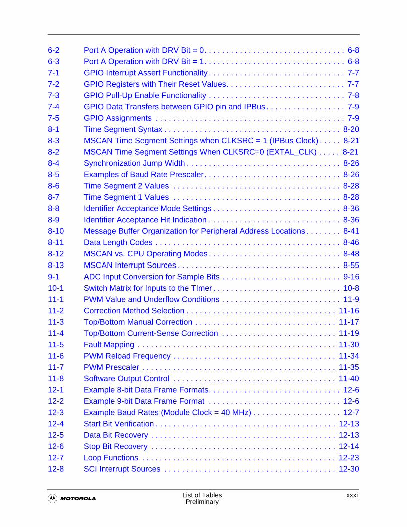
�List of Tables xxxiPreliminary
6-2 Port A Operation with DRV Bit = 0. . . . . . . . . . . . . . . . . . . . . . . . . . . . . . . . 6-86-3 Port A Operation with DRV Bit = 1. . . . . . . . . . . . . . . . . . . . . . . . . . . . . . . . 6-87-1 GPIO Interrupt Assert Functionality . . . . . . . . . . . . . . . . . . . . . . . . . . . . . . . 7-77-2 GPIO Registers with Their Reset Values. . . . . . . . . . . . . . . . . . . . . . . . . . . 7-77-3 GPIO Pull-Up Enable Functionality . . . . . . . . . . . . . . . . . . . . . . . . . . . . . . . 7-87-4 GPIO Data Transfers between GPIO pin and IPBus . . . . . . . . . . . . . . . . . . 7-97-5 GPIO Assignments . . . . . . . . . . . . . . . . . . . . . . . . . . . . . . . . . . . . . . . . . . . 7-98-1 Time Segment Syntax . . . . . . . . . . . . . . . . . . . . . . . . . . . . . . . . . . . . . . . . 8-208-3 MSCAN Time Segment Settings when CLKSRC = 1 (IPBus Clock) . . . . . 8-218-2 MSCAN Time Segment Settings When CLKSRC=0 (EXTAL_CLK) . . . . . 8-218-4 Synchronization Jump Width . . . . . . . . . . . . . . . . . . . . . . . . . . . . . . . . . . . 8-268-5 Examples of Baud Rate Prescaler. . . . . . . . . . . . . . . . . . . . . . . . . . . . . . . 8-268-6 Time Segment 2 Values . . . . . . . . . . . . . . . . . . . . . . . . . . . . . . . . . . . . . . 8-288-7 Time Segment 1 Values . . . . . . . . . . . . . . . . . . . . . . . . . . . . . . . . . . . . . . 8-288-8 Identifier Acceptance Mode Settings . . . . . . . . . . . . . . . . . . . . . . . . . . . . . 8-368-9 Identifier Acceptance Hit Indication . . . . . . . . . . . . . . . . . . . . . . . . . . . . . . 8-368-10 Message Buffer Organization for Peripheral Address Locations . . . . . . . . 8-418-11 Data Length Codes . . . . . . . . . . . . . . . . . . . . . . . . . . . . . . . . . . . . . . . . . . 8-468-12 MSCAN vs. CPU Operating Modes . . . . . . . . . . . . . . . . . . . . . . . . . . . . . . 8-488-13 MSCAN Interrupt Sources . . . . . . . . . . . . . . . . . . . . . . . . . . . . . . . . . . . . . 8-559-1 ADC Input Conversion for Sample Bits . . . . . . . . . . . . . . . . . . . . . . . . . . . 9-1610-1 Switch Matrix for Inputs to the TImer . . . . . . . . . . . . . . . . . . . . . . . . . . . . . 10-811-1 PWM Value and Underflow Conditions . . . . . . . . . . . . . . . . . . . . . . . . . . . 11-911-2 Correction Method Selection . . . . . . . . . . . . . . . . . . . . . . . . . . . . . . . . . . 11-1611-3 Top/Bottom Manual Correction . . . . . . . . . . . . . . . . . . . . . . . . . . . . . . . . 11-1711-4 Top/Bottom Current-Sense Correction . . . . . . . . . . . . . . . . . . . . . . . . . . 11-1911-5 Fault Mapping . . . . . . . . . . . . . . . . . . . . . . . . . . . . . . . . . . . . . . . . . . . . . 11-3011-6 PWM Reload Frequency . . . . . . . . . . . . . . . . . . . . . . . . . . . . . . . . . . . . . 11-3411-7 PWM Prescaler . . . . . . . . . . . . . . . . . . . . . . . . . . . . . . . . . . . . . . . . . . . . 11-3511-8 Software Output Control . . . . . . . . . . . . . . . . . . . . . . . . . . . . . . . . . . . . . 11-4012-1 Example 8-bit Data Frame Formats. . . . . . . . . . . . . . . . . . . . . . . . . . . . . . 12-612-2 Example 9-bit Data Frame Format . . . . . . . . . . . . . . . . . . . . . . . . . . . . . . 12-612-3 Example Baud Rates (Module Clock = 40 MHz) . . . . . . . . . . . . . . . . . . . . 12-712-4 Start Bit Verification . . . . . . . . . . . . . . . . . . . . . . . . . . . . . . . . . . . . . . . . . 12-1312-5 Data Bit Recovery . . . . . . . . . . . . . . . . . . . . . . . . . . . . . . . . . . . . . . . . . . 12-1312-6 Stop Bit Recovery . . . . . . . . . . . . . . . . . . . . . . . . . . . . . . . . . . . . . . . . . . 12-1412-7 Loop Functions . . . . . . . . . . . . . . . . . . . . . . . . . . . . . . . . . . . . . . . . . . . . 12-2312-8 SCI Interrupt Sources . . . . . . . . . . . . . . . . . . . . . . . . . . . . . . . . . . . . . . . 12-30
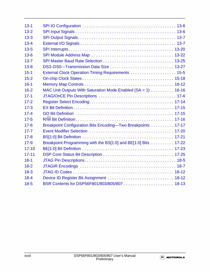
xxxii DSP56F801/803/805/807 User’s Manual�Preliminary
13-1 SPI IO Configuration . . . . . . . . . . . . . . . . . . . . . . . . . . . . . . . . . . . . . . . . . 13-613-2 SPI Input Signals . . . . . . . . . . . . . . . . . . . . . . . . . . . . . . . . . . . . . . . . . . . . 13-613-3 SPI Output Signals. . . . . . . . . . . . . . . . . . . . . . . . . . . . . . . . . . . . . . . . . . . 13-713-4 External I/O Signals . . . . . . . . . . . . . . . . . . . . . . . . . . . . . . . . . . . . . . . . . . 13-713-5 SPI Interrupts . . . . . . . . . . . . . . . . . . . . . . . . . . . . . . . . . . . . . . . . . . . . . . 13-2013-6 SPI Module Address Map . . . . . . . . . . . . . . . . . . . . . . . . . . . . . . . . . . . . 13-2213-7 SPI Master Baud Rate Selection . . . . . . . . . . . . . . . . . . . . . . . . . . . . . . . 13-2513-8 DS3–DS0—Transmission Data Size . . . . . . . . . . . . . . . . . . . . . . . . . . . . 13-2715-1 External Clock Operation Timing Requirements . . . . . . . . . . . . . . . . . . . . 15-515-2 On-chip Clock States . . . . . . . . . . . . . . . . . . . . . . . . . . . . . . . . . . . . . . . . 15-1816-1 Memory Map Controls . . . . . . . . . . . . . . . . . . . . . . . . . . . . . . . . . . . . . . . 16-1216-2 MAC Unit Outputs With Saturation Mode Enabled (SA = 1) . . . . . . . . . . 16-1617-1 JTAG/OnCE Pin Descriptions . . . . . . . . . . . . . . . . . . . . . . . . . . . . . . . . . . 17-617-2 Register Select Encoding. . . . . . . . . . . . . . . . . . . . . . . . . . . . . . . . . . . . . 17-1417-3 EX Bit Definition . . . . . . . . . . . . . . . . . . . . . . . . . . . . . . . . . . . . . . . . . . . . 17-1517-4 GO Bit Definition . . . . . . . . . . . . . . . . . . . . . . . . . . . . . . . . . . . . . . . . . . . 17-1517-5 R/W Bit Definition. . . . . . . . . . . . . . . . . . . . . . . . . . . . . . . . . . . . . . . . . . . 17-1617-6 Breakpoint Configuration Bits Encoding—Two Breakpoints . . . . . . . . . . 17-1717-7 Event Modifier Selection . . . . . . . . . . . . . . . . . . . . . . . . . . . . . . . . . . . . . 17-2017-8 BS[1:0] Bit Definition . . . . . . . . . . . . . . . . . . . . . . . . . . . . . . . . . . . . . . . . 17-2117-9 Breakpoint Programming with the BS[1:0] and BE[1:0] Bits . . . . . . . . . . 17-2217-10 BE[1:0] Bit Definition . . . . . . . . . . . . . . . . . . . . . . . . . . . . . . . . . . . . . . . . 17-2317-11 DSP Core Status Bit Description . . . . . . . . . . . . . . . . . . . . . . . . . . . . . . . 17-2518-1 JTAG Pin Descriptions. . . . . . . . . . . . . . . . . . . . . . . . . . . . . . . . . . . . . . . . 18-518-2 JTAGIR Encodings . . . . . . . . . . . . . . . . . . . . . . . . . . . . . . . . . . . . . . . . . . 18-718-3 JTAG ID Codes . . . . . . . . . . . . . . . . . . . . . . . . . . . . . . . . . . . . . . . . . . . . 18-1218-4 Device ID Register Bit Assignment . . . . . . . . . . . . . . . . . . . . . . . . . . . . . 18-1218-5 BSR Contents for DSP56F801/803/805/807 . . . . . . . . . . . . . . . . . . . . . . 18-13

�DSP56F801/803/805/807 Overview 1-1
Preliminary
1
Chapter 1DSP56F801/803/805/807 Overview

1-2 DSP56F801/803/805/807 User’s Manual�Preliminary
1
Introduction
�DSP56F801/803/805/807 Overview 1-3
Preliminary
1
1.1 Introduction
Differing in size of memories and choice of peripherals, these multi-functional chips offer exceptional application control using a Motorola-patented synchronization of the Pulse Width Modulator and Analog-to-Digital Converter. The core provides more processing power than any other control chip while saving design space and money. The DSP56F801, DSP56F803, DSP56F805, and DSP56F807 are members of the DSP56800 core-based family of Digital Signal Processors (DSPs). Combined on a single chip are the processing power of a DSP and the functionality of a micro controller and a flexible set of peripherals. The chip design creates an extremely cost-effective and compact solution for a number of uses. The family of chips will provide control for such applications as:
• AC Induction Motors (industrial and appliance--washing machines, HVAC, fans, vacuums, and motor drives
• Brush DC Motors—car window lifters and electric antennas, toys, cordless tools
• Brushless DC Motors (automotive and appliance)—PC fans, ceiling fans, blowers, washing machines, electric power steering systems
• Switched and Variable Reluctance Motors—washing machines, electric power steering, dynamic body control, refrigerator compressors, HVAC, fans, vacuums and for the power control for:
• General Converter/Inverter applications
• Uninterruptable Power Systems—in-line, line interactive, and standby
• Inverter Output Stages—push-pull, half-bridge, and full bridge
Want to know more? Each of the four chips may be designed, at the minimum, into the following applications:
• Precision Motor Control of all types, AC, DC, Brush, Brushless, Polyphase, and Switched Reluctance
• Automotive Control
• Power Line Modem
• Uninterruptable Power Supplies
• Telephony System Implementation
• Noise Cancellation Applications
• Home Security
• Temperature Regulation
• HVAC Applications
1-4 DSP56F801/803/805/807 User’s Manual�Preliminary
Introduction1
• Remote Monitoring and Control
• Digital Telephone Answering Machine
• Fuel Management Systems
• Voice Enabled Appliances
• Cable Test Equipment
• Electric Energy Meter with Embedded Power line Modem
• Underwater Acoustics
• Glass Breakage Detection and Security Systems
• Traffic Light Control
• Identification Tag Readers
In addition to the above general functions of each chip, the following are unique to a specific chip:
DSP56F801 Unique applications include:
• Steppers and Encoders
• Home Appliances Controls Integrated with voice Control
• Smart Appliances
• Home Security
• Digital Telephone Answering Machine
• Engine Management
• Power Line Modem
• Servo Drives
• Winder/Pullers
DSP56F803 Unique applications include:
• Steppers and Encoders
• Smart Appliances
• Home Appliances Controls Integrated with voice Control
• Home Security
• Servo Drives
• Exercise Equipment
• Digital Telephone Answering Machine
DSP56800 Family Description
�DSP56F801/803/805/807 Overview 1-5
Preliminary
1
• Power Line Modem
• Winder and Pullers
• Lifts, Elevators and Cranes
DSP56F805 Unique applications include:
• Steppers and Encoders
• Servo Drives
• Digital Telephone Answering Machine
• Home Security
• Power Line Modem
• Home Appliances Controls Integrated with voice Control
• Exercise Equipment
• Winder and Pullers
• Lifts, Elevators and Cranes
• Frequency Converters and Voltage Investors
DSP56F807 Unique applications include:
• Steppers and Encoders
• Power Line Modem
• Home Appliances Controls Integrated with voice Control
• Engine Management
• Digital Telephone Answering Machine
• Home Security
• Lifts, Elevators and Cranes
• Frequency Converters and Voltage Investors
1.2 DSP56800 Family Description
The DSP56800 core is based on a Harvard architecture consisting of three execution units operating in parallel. The MCU-style programming model and optimized instruction set allow straightforward generation of efficient, compact DSP and control code. The instruction set is highly efficient for C Compilers, enabling rapid development of optimized control applications.
1-6 DSP56F801/803/805/807 User’s Manual�Preliminary
DSP56800 Family Description1
The DSP56F/803/805/807 chips support program execution from either internal or external memories, providing two-external dedicated interrupt lines and up to 32 General-Purpose Input/Output (GPIO) lines. The DSP controller includes Program Flash and Data Flash, each programmable through the JTAG port, with Program RAM and Data RAM. With the exception of the 801, the controller also supports program execution for external memory. The DSP56800 core is capable of accessing two data operands from the on-chip Data RAM per instruction cycle.
A Boot Flash is incorporated for easy customer-inclusion of field-programmable software routines and can be used to program the main Program and Data Flash memory areas. Both Program and Flash memories can be both bulk and page erased; however, while erasure is being performed on the main Program and /or Data Flash memories, the Boot Flash should not be erased. All flash memories can be erased at once, if executing from a programmable RAM.
A key application-specific feature of the device is the inclusion of Pulse Width Modulator (PWM) modules. These modules each incorporate three complementary, individually programmable PWM signal outputs. To enhance motor control functionality, each module, except the 801,is also capable of supporting six independent PWM functions, for a total of 12 PWM outputs. Complementary operation permits programmable dead-time insertion, distortion correction through current sensing by software, and separate top and bottom output polarity control. The up-counter value is programmable to support a continuously variable PWM frequency. Both edge- and center-aligned synchronous pulse width-control, full zero percent to 100 percent modulation, are supported. The device is capable of controlling most motor types: AC Induction Motors (ACIM), both Brushless (BLDC) and Brush DC motors (BDC), Switched (SRM) and Variable Reluctance Motors (VRM), and Stepper motors.
Fault protection and cycle-by-cycle current limiting are incorporated in PWMs with sufficient output drive capability to directly drive standard opto-isolators. A smoke-inhibit write-once protection feature for key parameters is also included. And a patented PWM waveform distortion correction circuit is provided as well. Each PWM is double-buffered and includes interrupt controls permitting integral reload rates programmable from 1 to 16. The PWM modules provide a reference output to synchronize the Analog-to-Digital Converters.
Feature parts incorporated in the DSP56F801/803/805/807 are: 1) several 4-input multiplexed; and 2) 12-bit Analog-to-Digital Converters (ADC) and Quadrature Decoders. Each is capable of capturing transitions on the two-phase inputs, permitting generation of a number proportional to actual position. Speed computation capabilities accommodate both fast and slow moving shafts. The integrated watchdog timer in the Quadrature Decoder can be programmed with a time-out value to alarm when no shaft motion is detected. Each input is filtered ensuring only true transitions are recorded. If
Manual Organization
�DSP56F801/803/805/807 Overview 1-7
Preliminary
1
any Quadrature Decoder is not required, it can be programmed to provide a Quad Timer alternate function using four 16-bit independent timers. The DSP controller also provides a full set of standard programmable peripherals: Serial Communications Interfaces (SCI), Serial Peripheral Interface (SPI), and additional Quad Timers. Any of these interfaces can be used as General Purpose Input/Outputs (GPIOs) if that function is not required. A Controller Area
Network interface, CAN version 2.0 A/B-compliant, an internal interrupt controller and dedicated GPIO, are also included on some of the parts.
1.3 Manual Organization
This manual is arranged in the following sections:
• Chapter 1, DSP56F801/803/805/807 Overview—provides a brief overview of the DSP56F801, DSP56F803, DSP56F805, and DSP56F807. The chapter describes the structure of this document, and lists other documentation necessary to use these chips
• Chapter 2, Pin Descriptions—provides a description of the pins on the DSP56F801/803/805/807 chips and how the pins are grouped into the various interfaces
• Chapter 3, Memory and Operating Modes—describes the on-chip memory, structures, registers, and interfaces
• Chapter 4, Interrupt Controller (ITCN)—describes how the IPBus Interrupt Controller accepts interrupt requests from IPBus-based peripherals and presents them to the DSP56800 core
• Chapter 5, Flash Memory Interface—describes the Program Flash, Data Flash, and Boot Flash features and registers
• Chapter 6, External Memory Interface—describes the external memory interface available on the DSP56F803, DSP56F805, and DSP56F807
• Chapter 7, General Purpose Input/Output (GPIO)—describes how the GPIO shares package pins with other peripherals on the chip
• Chapter 8, Motorola Scalable Controller Area Network (MSCAN)—describes the capabilities of CAN as a communication controller
• Chapter 9, Analog-to-Digital Converter (ADC)—describes features, functions and registers of the Analog-to-Digital Converter
• Chapter 10, Quadrature Decoder—describes the features and registers of the Quadrature Decoder
1-8 DSP56F801/803/805/807 User’s Manual�Preliminary
Manual Organization1
• Chapter 11, Pulse Width Modulator Module (PWM)—describes the function, configuration and registers of the PWM
• Chapter 12, Serial Communications Interface Module (SCI)—describes the Serial Communications Interface (SCI), communicating with devices such as codecs, other DSPs, microprocessors, and peripherals to provide the primary data input path
• Chapter 13, Serial Peripheral Interface (SPI)—describes the Serial Peripheral Interface (SPI), communicating with external devices, such as Liquid Crystal Displays (LCDs) and Micro controller Units (MCUs)
• Chapter 14, Quad Timer Module—describes the available internal Quad Timer devices, including features and registers
• Chapter 15, On-chip Clock Synthesis (OCCS)—describes the internal oscillator, Phase Lock Loop (PLL), and timer distribution chain for the DSP56F801/803/805/807
• Chapter 16, Reset, Low Voltage, Stop and Wait Operation—describes the on-chip Watchdog timer and the real-time interrupt generator, and the modes of operation
• Chapter 17, OnCE Module—describes the specifics of the DSP56F801/803/805/807 On-Chip Emulation (OnCE™) module, accessed through the Joint Test Action Group (JTAG) port
• Chapter 18, JTAG Port Introduction—describes the specifics of the DSP56F801/803/805/807 JTAG port
• Appendix A, Glossary—provides definitions of terms, acronyms and register names used in this manual
• Appendix B, BSDL Listing—provides a sample Boundary Scan Description Language (BSDL) listing for the DSP56F801/803/805/807
• Appendix C, Programmer’s Sheets—provides a set of reference tables and programming sheets that are intended to simplify programming for the DSP56F801/803/805/807
• Appendix D, Packaging & Pinout Information—provides succinct package and pin-out information about each product
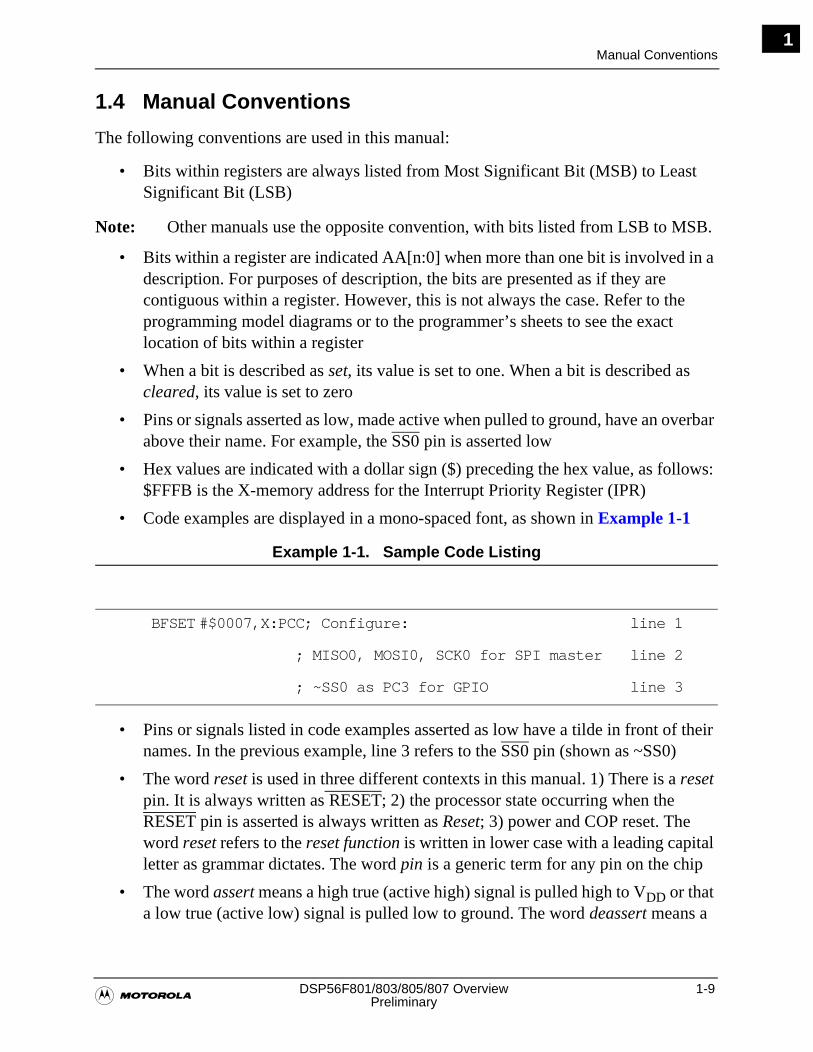
Manual Conventions
�DSP56F801/803/805/807 Overview 1-9
Preliminary
1
1.4 Manual Conventions
The following conventions are used in this manual:
• Bits within registers are always listed from Most Significant Bit (MSB) to Least Significant Bit (LSB)
Note: Other manuals use the opposite convention, with bits listed from LSB to MSB.
• Bits within a register are indicated AA[n:0] when more than one bit is involved in a description. For purposes of description, the bits are presented as if they are contiguous within a register. However, this is not always the case. Refer to the programming model diagrams or to the programmer’s sheets to see the exact location of bits within a register
• When a bit is described as set, its value is set to one. When a bit is described as cleared, its value is set to zero
• Pins or signals asserted as low, made active when pulled to ground, have an overbar above their name. For example, the SS0 pin is asserted low
• Hex values are indicated with a dollar sign ($) preceding the hex value, as follows: $FFFB is the X-memory address for the Interrupt Priority Register (IPR)
• Code examples are displayed in a mono-spaced font, as shown in Example 1-1
Example 1-1. Sample Code Listing
• Pins or signals listed in code examples asserted as low have a tilde in front of their names. In the previous example, line 3 refers to the SS0 pin (shown as ~SS0)
• The word reset is used in three different contexts in this manual. 1) There is a reset pin. It is always written as RESET; 2) the processor state occurring when the RESET pin is asserted is always written as Reset; 3) power and COP reset. The word reset refers to the reset function is written in lower case with a leading capital letter as grammar dictates. The word pin is a generic term for any pin on the chip
• The word assert means a high true (active high) signal is pulled high to VDD or that a low true (active low) signal is pulled low to ground. The word deassert means a
BFSET #$0007,X:PCC; Configure: line 1
; MISO0, MOSI0, SCK0 for SPI master line 2
; ~SS0 as PC3 for GPIO line 3
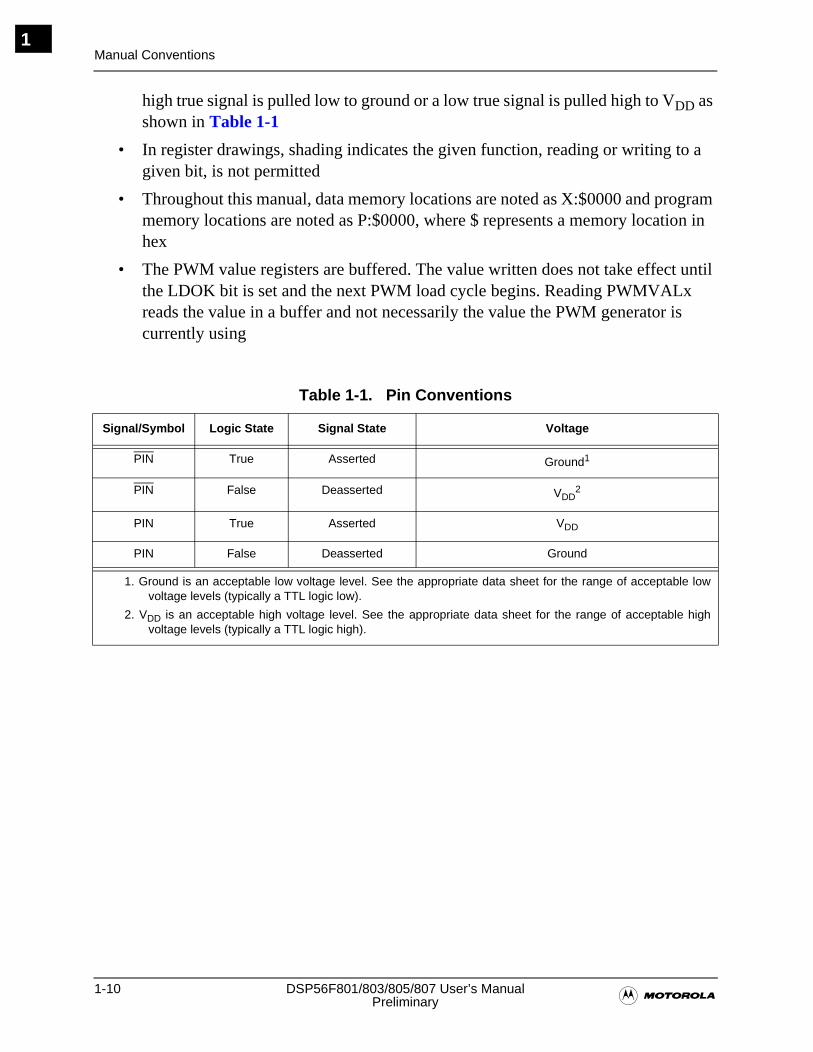
1-10 DSP56F801/803/805/807 User’s Manual�Preliminary
Manual Conventions1
high true signal is pulled low to ground or a low true signal is pulled high to VDD as shown in Table 1-1
• In register drawings, shading indicates the given function, reading or writing to a given bit, is not permitted
• Throughout this manual, data memory locations are noted as X:$0000 and program memory locations are noted as P:$0000, where $ represents a memory location in hex
• The PWM value registers are buffered. The value written does not take effect until the LDOK bit is set and the next PWM load cycle begins. Reading PWMVALx reads the value in a buffer and not necessarily the value the PWM generator is currently using
Table 1-1. Pin Conventions
Signal/Symbol Logic State Signal State Voltage
PIN True Asserted Ground1
PIN False Deasserted VDD2
PIN True Asserted VDD
PIN False Deasserted Ground
1. Ground is an acceptable low voltage level. See the appropriate data sheet for the range of acceptable lowvoltage levels (typically a TTL logic low).
2. VDD is an acceptable high voltage level. See the appropriate data sheet for the range of acceptable highvoltage levels (typically a TTL logic high).
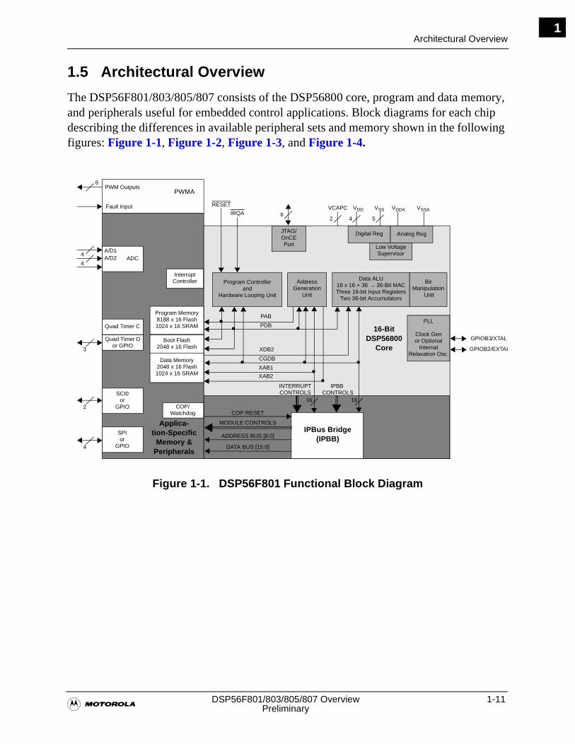
Architectural Overview
�DSP56F801/803/805/807 Overview 1-11
Preliminary
1
1.5 Architectural Overview
The DSP56F801/803/805/807 consists of the DSP56800 core, program and data memory, and peripherals useful for embedded control applications. Block diagrams for each chip describing the differences in available peripheral sets and memory shown in the following figures: Figure 1-1, Figure 1-2, Figure 1-3, and Figure 1-4.
Figure 1-1. DSP56F801 Functional Block Diagram
JTAG/OnCE Port
Digital Reg Analog Reg
Low VoltageSupervisor
Program Controllerand
Hardware Looping Unit
Data ALU16 x 16 + 36 → 36-Bit MACThree 16-bit Input Registers
Two 36-bit Accumulators
Address Generation
Unit
Bit Manipulation
Unit
PLL
Clock Genor Optional
InternalRelaxation Osc.
16-BitDSP56800
Core
PAB
PDB
XDB2
CGDB
XAB1
XAB2
GPIOB3/XTAL
GPIOB2/EXTAL
INTERRUPT CONTROLS
IPBB CONTROLS
IPBus Bridge (IPBB)
MODULE CONTROLS
ADDRESS BUS [8:0]
DATA BUS [15:0]
COP RESET
RESET
IRQA
Applica-tion-Specific
Memory &Peripherals
Interrupt Controller
Program Memory8188 x 16 Flash1024 x 16 SRAM
Boot Flash2048 x 16 Flash
Data Memory2048 x 16 Flash1024 x 16 SRAM
COP/Watchdog
SPIor
GPIO
SCI0or
GPIO
Quad Timer Dor GPIO
Quad Timer C
A/D1A/D2 ADC
4
2
3
4
4
6PWM Outputs
Fault Input
PWMA
16 16
VCAPC VDD VSS VDDA VSSA6
2 4 5
• •
•
•
••
•
•
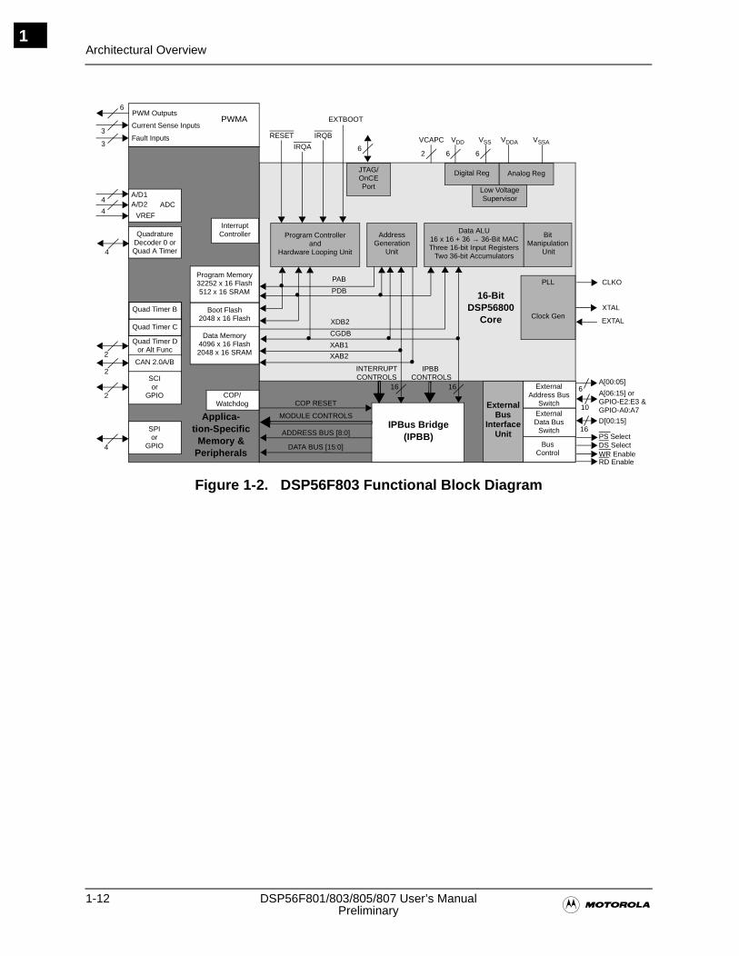
1-12 DSP56F801/803/805/807 User’s Manual�Preliminary
Architectural Overview1
Figure 1-2. DSP56F803 Functional Block Diagram
JTAG/OnCE Port
Digital Reg Analog Reg
Low VoltageSupervisor
Program Controllerand
Hardware Looping Unit
Data ALU16 x 16 + 36 → 36-Bit MACThree 16-bit Input Registers
Two 36-bit Accumulators
Address Generation
Unit
Bit Manipulation
Unit
PLL
Clock Gen
16-BitDSP56800
Core
PAB
PDB
XDB2
CGDB
XAB1
XAB2
XTAL
EXTAL
INTERRUPT CONTROLS
IPBB CONTROLS
IPBus Bridge (IPBB)
MODULE CONTROLS
ADDRESS BUS [8:0]
DATA BUS [15:0]
COP RESET
RESET
IRQA
IRQB
Applica-tion-Specific
Memory &Peripherals
Interrupt Controller
Program Memory32252 x 16 Flash512 x 16 SRAM
Boot Flash2048 x 16 Flash
Data Memory4096 x 16 Flash2048 x 16 SRAM
COP/Watchdog
SPIor
GPIO
SCIor
GPIO
Quad Timer Dor Alt Func
A/D1A/D2 ADC
4
2
2
4
4
3
6PWM Outputs
Fault Inputs
PWMA
16 16
VCAPC VDD VSS VDDA VSSA6
2 6 6
• •
•
•
••
••
EXTBOOTCurrent Sense Inputs
3
QuadratureDecoder 0 orQuad A Timer
CAN 2.0A/B2
CLKO
ExternalAddress Bus
Switch
BusControl
ExternalData Bus
Switch
ExternalBus
InterfaceUnit
RD EnableWR EnableDS SelectPS Select
10
16
6A[00:05]
D[00:15]
A[06:15] orGPIO-E2:E3 &GPIO-A0:A7
4
Quad Timer C
VREF
Quad Timer B
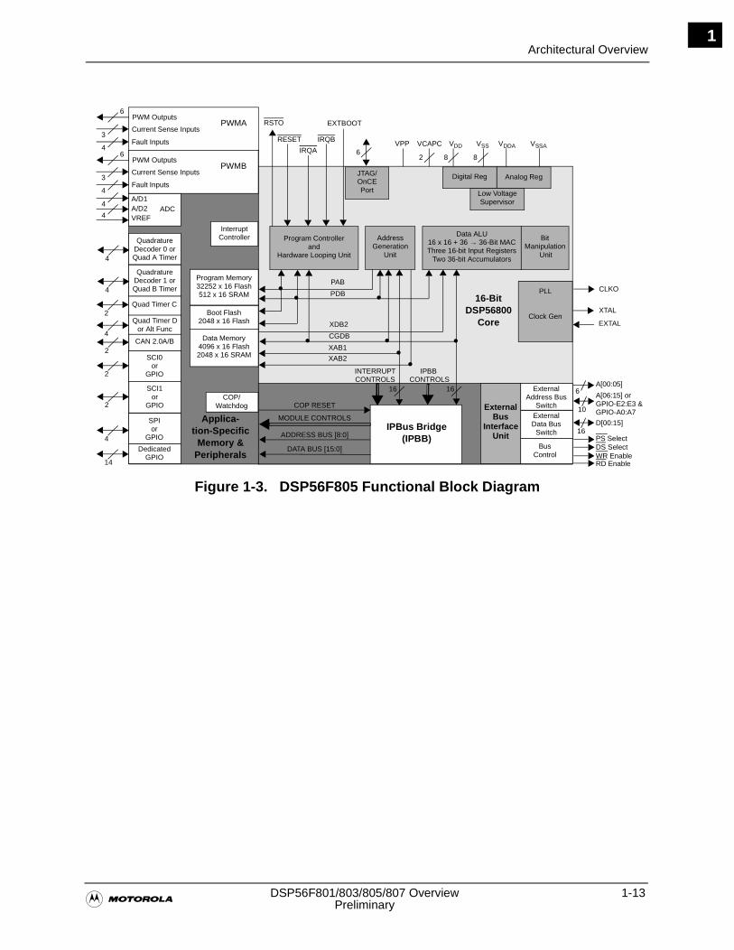
Architectural Overview
�DSP56F801/803/805/807 Overview 1-13
Preliminary
1
Figure 1-3. DSP56F805 Functional Block Diagram
JTAG/OnCE Port
Digital Reg Analog Reg
Low VoltageSupervisor
Program Controllerand
Hardware Looping Unit
Data ALU16 x 16 + 36 → 36-Bit MACThree 16-bit Input Registers
Two 36-bit Accumulators
Address Generation
Unit
Bit Manipulation
Unit
PLL
Clock Gen
16-BitDSP56800
Core
PAB
PDB
XDB2
CGDB
XAB1
XAB2
XTAL
EXTAL
INTERRUPT CONTROLS
IPBB CONTROLS
IPBus Bridge (IPBB)
MODULE CONTROLS
ADDRESS BUS [8:0]
DATA BUS [15:0]
COP RESET
RESET
IRQA
IRQB
Applica-tion-Specific
Memory &Peripherals
Interrupt Controller
Program Memory32252 x 16 Flash512 x 16 SRAM
Boot Flash2048 x 16 Flash
Data Memory4096 x 16 Flash2048 x 16 SRAM
COP/Watchdog
SPIor
GPIO
SCI0or
GPIO
Quad Timer Dor Alt Func
Quad Timer C
A/D1A/D2 ADC
4
2
4
4
4
4
6PWM Outputs
Fault Inputs
PWMA
16 16
VCAPC VDD VSS VDDA VSSA6
2 8 8
• •
•
•
••
••
EXTBOOTCurrent Sense Inputs
3
QuadratureDecoder 0 orQuad A Timer
CAN 2.0A/B2
CLKO
ExternalAddress Bus
Switch
BusControl
ExternalData Bus
Switch
ExternalBus
InterfaceUnit
RD EnableWR EnableDS SelectPS Select
10
16
6A[00:05]
D[00:15]
A[06:15] orGPIO-E2:E3 &GPIO-A0:A7
4
4
6PWM Outputs
Fault Inputs
PWMBCurrent Sense Inputs
3
QuadratureDecoder 1 orQuad B Timer4
2
SCI1or
GPIO2
DedicatedGPIO
14
VPP
RSTO
VREF
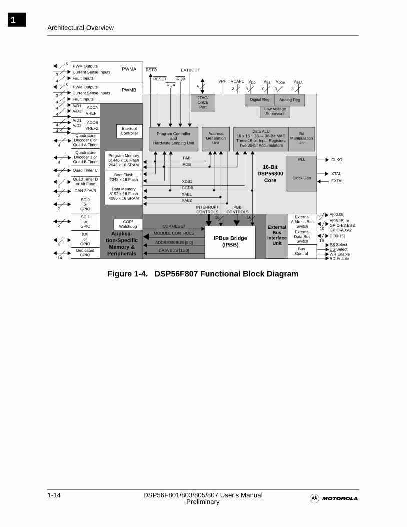
1-14 DSP56F801/803/805/807 User’s Manual�Preliminary
Architectural Overview1
Figure 1-4. DSP56F807 Functional Block Diagram
JTAG/OnCE Port
Digital Reg Analog Reg
Low VoltageSupervisor
Program Controllerand
Hardware Looping Unit
Data ALU16 x 16 + 36 → 36-Bit MACThree 16-bit Input Registers
Two 36-bit Accumulators
Address Generation
Unit
Bit Manipulation
Unit
PLL
Clock Gen
16-BitDSP56800
Core
PAB
PDB
XDB2
CGDB
XAB1
XAB2
XTAL
EXTAL
INTERRUPT CONTROLS
IPBB CONTROLS
IPBus Bridge (IPBB)
MODULE CONTROLS
ADDRESS BUS [8:0]
DATA BUS [15:0]
COP RESET
RESET
IRQA
IRQB
Applica-tion-Specific
Memory &Peripherals
Interrupt Controller
Program Memory61440 x 16 Flash2048 x 16 SRAM
Boot Flash2048 x 16 Flash
Data Memory8192 x 16 Flash4096 x 16 SRAM
COP/Watchdog
SPIor
GPIO
SCI0or
GPIO
Quad Timer Dor Alt Func
Quad Timer C
A/D1A/D2
ADCA
4
2
4
4
4
4
6PWM Outputs
Fault Inputs
PWMA
16 16
VCAPC VDD VSS VDDA VSSA6
2 8 10 3
• •
•
•
••
••
EXTBOOTCurrent Sense Inputs3
QuadratureDecoder 0 orQuad A Timer
CAN 2.0A/B2
CLKO
ExternalAddress Bus
Switch
BusControl
ExternalData Bus
Switch
ExternalBus
InterfaceUnit
RD EnableWR EnableDS SelectPS Select
10
16
6A[00:05]
D[00:15]
A[06:15] orGPIO-E2:E3 &GPIO-A0:A7
4
4
6PWM Outputs
Fault Inputs
PWMBCurrent Sense Inputs
3
QuadratureDecoder 1 orQuad B Timer4
2
SCI1or
GPIO2
DedicatedGPIO
14
VPP
RSTO
A/D1A/D2
ADCB
4
4
3
VREF2
VREF
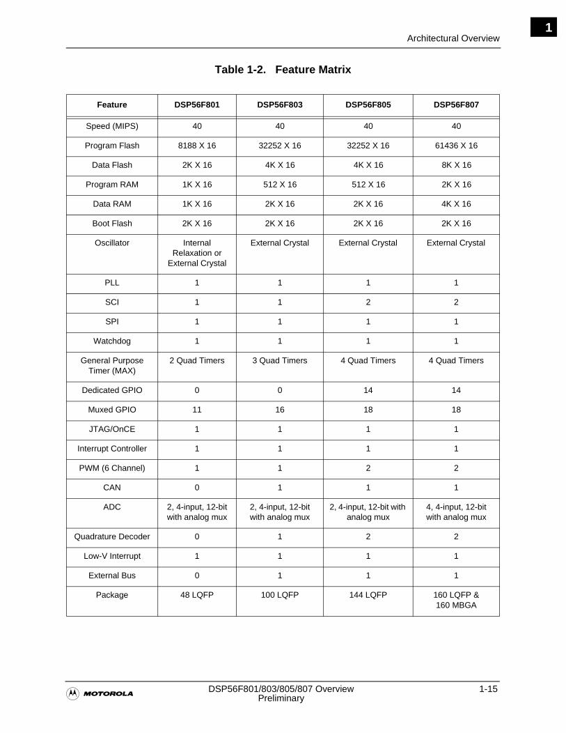
Architectural Overview
�DSP56F801/803/805/807 Overview 1-15
Preliminary
1
Table 1-2. Feature Matrix
Feature DSP56F801 DSP56F803 DSP56F805 DSP56F807
Speed (MIPS) 40 40 40 40
Program Flash 8188 X 16 32252 X 16 32252 X 16 61436 X 16
Data Flash 2K X 16 4K X 16 4K X 16 8K X 16
Program RAM 1K X 16 512 X 16 512 X 16 2K X 16
Data RAM 1K X 16 2K X 16 2K X 16 4K X 16
Boot Flash 2K X 16 2K X 16 2K X 16 2K X 16
Oscillator Internal Relaxation or
External Crystal
External Crystal External Crystal External Crystal
PLL 1 1 1 1
SCI 1 1 2 2
SPI 1 1 1 1
Watchdog 1 1 1 1
General Purpose Timer (MAX)
2 Quad Timers 3 Quad Timers 4 Quad Timers 4 Quad Timers
Dedicated GPIO 0 0 14 14
Muxed GPIO 11 16 18 18
JTAG/OnCE 1 1 1 1
Interrupt Controller 1 1 1 1
PWM (6 Channel) 1 1 2 2
CAN 0 1 1 1
ADC 2, 4-input, 12-bit with analog mux
2, 4-input, 12-bit with analog mux
2, 4-input, 12-bit with analog mux
4, 4-input, 12-bit with analog mux
Quadrature Decoder 0 1 2 2
Low-V Interrupt 1 1 1 1
External Bus 0 1 1 1
Package 48 LQFP 100 LQFP 144 LQFP 160 LQFP & 160 MBGA
1-16 DSP56F801/803/805/807 User’s Manual�Preliminary
DSP56800 Core Description1
1.6 DSP56800 Core Description
The DSP56800 core consists of functional units operating in parallel to increase throughput of the machine. The DSP56800 core consists of three execution units operating in parallel. These units allow as many as six operations during each instruction cycle. The MPU-style programming model and optimized instruction set allow straightforward generation of efficient, compact DSP and control code. The instruction set is also highly efficient for C Compilers. Major features of the DSP56800 core include the following:
• Efficient 16-bit DSP56800 family DSP engine with dual Harvard architecture
• As many as 40 Million Instructions Per Second (MIPS) at 80 MHz core frequency
• Single-cycle 16- × 16-bit parallel Multiplier-Accumulator (MAC)
• Two 36-bit accumulators, including extension bits
• 16-bit bidirectional barrel shifter
• Parallel instruction set with unique DSP addressing modes
• Hardware DO and REP loops
• Three internal address buses and one external address bus available
• Four internal data buses and one external data bus available
• Instruction set supports both DSP and controller functions
• Controller style addressing modes and instructions for compact code
• Efficient C Compiler and local variable support
• Software subroutine and interrupt stack with depth limited only by memory
• JTAG/OnCE debug programming interface
1.6.1 DSP56800 Core Differences
The DSP56800 core is used differently for the DSP56F801/803/805/807 from the way it was used in previous parts. Please note the following differences:
• Extensions for interrupt handling
• Bottom two bits of the BCR wait state fields are hardcoded to 0
• Optional disable for Stop and Wait modes
• MODA and MODB inputs have been replaced with EXTBOOT
• Disabled op code fetches from data memory space
• Fetches from Data Flash occur from either CGDB or XAB2, only one at a time
DSP56800 Core Description
�DSP56F801/803/805/807 Overview 1-17
Preliminary
1
• IPBus methodology used for most communication between the core and peripherals
• Single stage PLL with 8 MHz clock requirement
1.6.2 DSP56800 Core Block Diagram
An overall block diagram of the DSP56800 core architecture is shown in Figure 1-5. The DSP56800 core is fed by an internal program and data memory, an external memory interface, and various peripherals suitable for embedded applications. The blocks of the DSP56800 core include the following:
• Data Arithmetic Logic Unit (Data ALU)
• Address Generation Unit (AGU)
• Program Controller and Hardware Looping Unit
• Bit Manipulation Unit
• OnCE Port
• Interrupt Controller
• External Bus Bridge
• Address buses
• Data buses
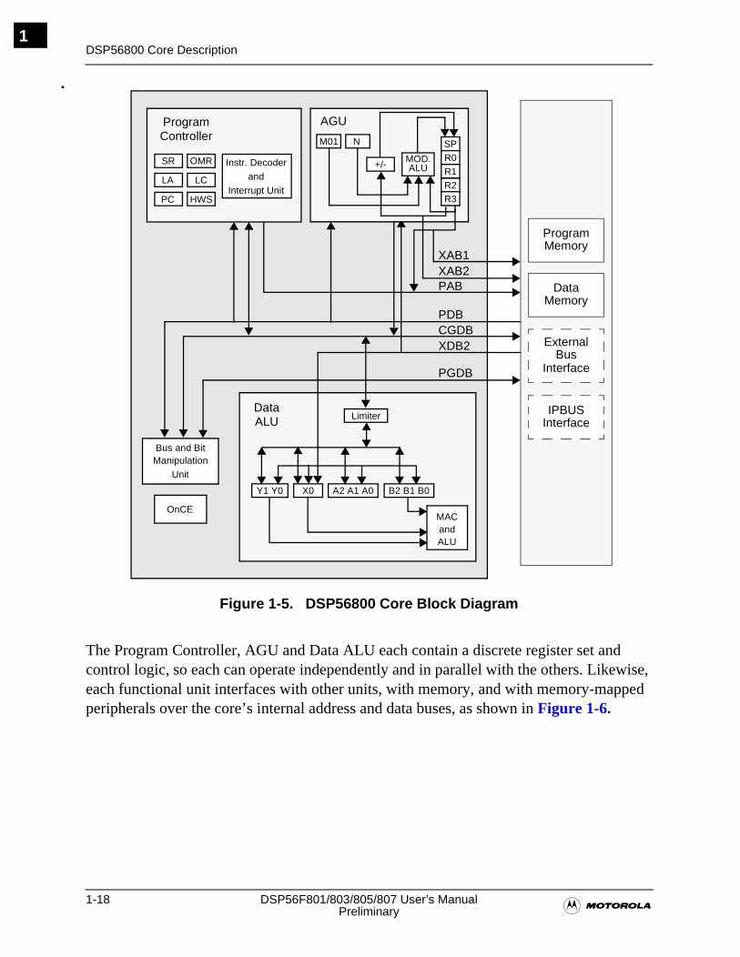
1-18 DSP56F801/803/805/807 User’s Manual�Preliminary
DSP56800 Core Description1
Figure 1-5. DSP56800 Core Block Diagram
The Program Controller, AGU and Data ALU each contain a discrete register set and control logic, so each can operate independently and in parallel with the others. Likewise, each functional unit interfaces with other units, with memory, and with memory-mapped peripherals over the core’s internal address and data buses, as shown in Figure 1-6.
CGDBPDB
PABXAB2XAB1
XDB2
PGDB
ProgramMemory
DataMemory
IPBUSInterface
ExternalBus
Interface
Instr. Decoder
and
Interrupt Unit
ProgramController
OMR
PC
LA LC
SR
HWS
SPR0R1R2
MOD.ALU+/-
AGU
R3
M01 N
Bus and BitManipulation
Unit
OnCE
Y1 Y0
Limiter
X0 A2 A1 A0 B2 B1 B0
DataALU
MACandALU
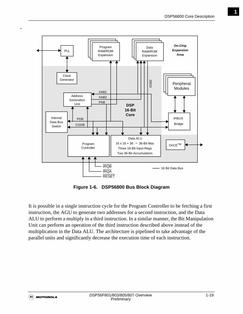
DSP56800 Core Description
�DSP56F801/803/805/807 Overview 1-19
Preliminary
1
It is possible in a single instruction cycle for the Program Controller to be fetching a first instruction, the AGU to generate two addresses for a second instruction, and the Data ALU to perform a multiply in a third instruction. In a similar manner, the Bit Manipulation Unit can perform an operation of the third instruction described above instead of the multiplication in the Data ALU. The architecture is pipelined to take advantage of the parallel units and significantly decrease the execution time of each instruction.
Figure 1-6. DSP56800 Bus Block Diagram
ProgramRAM/ROMExpansion
XAB1
XAB2
PAB
PDB
CGDB
IRQB
RESET
16 Bit Data BusIRQA
PeripheralModules
ExpansionArea
DSP16-BitCore
Program
Data ALU
16 x 16 + 36 → 36-Bit Mac
Three 16-Bit Input Regs
Two 36-Bit Accumulators
OnCETM
On-Chip
AddressGeneration
Unit
InternalData Bus
Switch
PLL
XD
B2
DataRAM/ROMExpansion
ClockGenerator
Controller
IPBUS
Bridge
1-20 DSP56F801/803/805/807 User’s Manual�Preliminary
DSP56800 Core Description1
1.6.3 Data Arithmetic Logic Unit (Data ALU)
The Data Arithmetic Logic Unit (Data ALU) performs all of the arithmetic and logical operations on data operands. It contains the following:
• Three 16-bit input registers
• Two 32-bit accumulator registers
• Two 4-bit accumulator extension registers
• One parallel, single cycle, non-pipelined MAC unit
• An accumulator shifter
• One data limiter
• One MAC output limiter
• One 16-bit barrel shifter
The Data ALU is capable of performing the following in one instruction cycle:
• Multiplication
• Multiply-accumulate with positive or negative accumulation
• Addition
• Subtraction
• Shifting
• Logical operations
Arithmetic operations are completed using two’s-complement fractional or integer arithmetic. Support is also provided for unsigned and multi-precision arithmetic.
Data ALU source operands can be 16, 32, or 36 bits and can originate from input registers and/or accumulators. ALU results are stored in one of the accumulators. In addition, some arithmetic instructions store their 16-bit results in any of the three Data ALU input registers or write directly to memory. Arithmetic operations and shifts have a 16-bit or 36-bit result, and logical operations are performed on 16-bit operands yielding 16-bit results. Data ALU registers can be read or written by the Core Global Data Bus (CGDB) as 16-bit operands, and the X0 register can also be written by the X Data Bus 2 (XDB2) with a 16-bit operand.
DSP56800 Core Description
�DSP56F801/803/805/807 Overview 1-21
Preliminary
1
1.6.4 Address Generation Unit (AGU)
The Address Generation Unit (AGU) performs all of the effective address calculations and address storage necessary to address data operands in memory. This unit operates in parallel with other chip resources to minimize address generation overhead. It contains two ALUs, allowing the generation of up to two 16-bit addresses every instruction cycle—one for either the XAB1 or PAB bus and one for the XAB2 bus. The ALU can directly address 65,536 locations on the XAB1 or XAB2 bus and 65,536 locations on the Program Address Bus (PAB), for a total capability of 131,072 16-bit data words. Hooks are provided on the DSP56800 core to expand this address space. Its arithmetic unit can perform linear and modulo arithmetic.
1.6.5 Program Controller and Hardware Looping Unit
The Program Controller performs:
• Instruction prefetch
• Instruction decoding
• Hardware loop control
• Interrupt (exception) processing
Instruction execution is carried out in other core units, such as the Data ALU or AGU. The Program Controller consists of a Program Counter (PC) unit, hardware looping control logic, interrupt control logic, and status and control registers.
Two interrupt control pins provide input to the program interrupt controller. The External Interrupt Request A (IRQA) pin and the External Interrupt Request B (IRQB) pin receive interrupt requests from external sources.
The RESET pin resets the DSP56F803/805/807. When it is asserted, it initializes the chip and places it in the Reset state. When the RESET pin is deasserted, the initial chip operating mode is latched into the Operating Mode Register (OMR) based upon the value present on the EXTBOOT pin. The DSP56F801 is internally pulled low. Refer to Section 3.3.2 for additional details.
1.6.6 Bit Manipulation Unit
The Bit Manipulation Unit performs bitfield manipulations on X-memory words, peripheral registers, and registers on the DSP56800 core. It is capable of testing, setting, clearing, or inverting any bits specified in a 16-bit mask. For branch-on-bitfield instructions, this unit tests bits on the upper or lower byte of a 16-bit word. In other words, the mask tests a maximum of 8 bits at a time.
1-22 DSP56F801/803/805/807 User’s Manual�Preliminary
DSP56800 Core Description1
Transfers between buses are accomplished in the bus unit. The bus unit is similar to a switch matrix, and can connect any two of the three data buses together without adding any pipeline delays. This is required for transferring a core register to a peripheral register, for example, because the core register is connected to the CGDB bus.
As a general rule, when reading any register less than 16 bits wide, unused bits are read as zero. Reserved and unused bits should always be written with a zero ensuring future compatibility.
1.6.7 Address and Data Buses
Addresses are provided to the internal X-data memory on two unidirectional 16-bit buses—X Address Bus 1 (XAB1) and X Address Bus 2 (XAB2). Program memory addresses are provided on the unidirectional 19-bit Program Address Bus (PAB). Note the XAB1 can provide addresses for accessing both internal and external memory, whereas the XAB2 can only provide addresses for accessing internal read-only memory. The External Address Bus (EAB) provides addresses for external memory.
Data movement on the DSP56F801/803/805/807 occurs over three bidirectional 16-bit buses—the CGDB, the Program Data Bus (PDB), the PGDB, and also over one unidirectional 16-bit bus: the X Data Bus 2 (XDB2). When one memory access is performed, data transfer between the Data ALU and the X data memory occurs over the CGDB. When two simultaneous memory reads are performed transfers occur over the CGDB and the XDB2. All other data transfers to core blocks occur over the CGDB, transferring all to and from peripherals over the PGDB. Instruction word fetches occur simultaneously over the PDB. The External Data Bus (EDB) provides bidirectional access to external data memory.
The bus structure supports: 1) General register-to-register; 2) Register-to-memory; and 3) Memory-to-register transfers. Each can transfer up to three 16-bit words in the same instruction cycle. Transfers between buses are accomplished in the Bit Manipulation Unit. Table 1-3 lists the address and data buses for the DSP56800 core.
Table 1-3. DSP56800 Address and Data Buses
Bus Bus Name Bus Width, Direction, and Use
XAB1 X Address Bus 1 16-bit, unidirectional, internal and external memory address
XAB2 X Address Bus 2 16-bit, unidirectional, internal memory address
PAB Program Address Bus 16-bit, unidirectional, internal memory address
EAB External Address Bus 16-bit, unidirectional, external memory address
CGDB Core Global Data Bus 16-bit, bidirectional, internal data movement
PDB Program Data Bus 16-bit, bidirectional, instruction word fetches
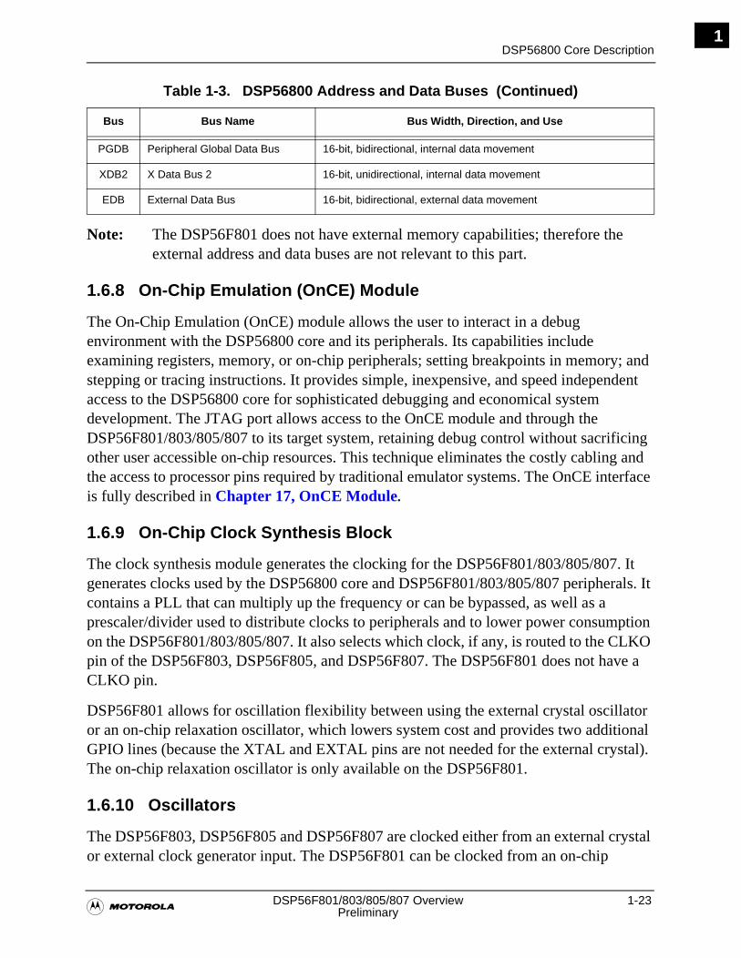
DSP56800 Core Description
�DSP56F801/803/805/807 Overview 1-23
Preliminary
1
Note: The DSP56F801 does not have external memory capabilities; therefore the external address and data buses are not relevant to this part.
1.6.8 On-Chip Emulation (OnCE) Module
The On-Chip Emulation (OnCE) module allows the user to interact in a debug environment with the DSP56800 core and its peripherals. Its capabilities include examining registers, memory, or on-chip peripherals; setting breakpoints in memory; and stepping or tracing instructions. It provides simple, inexpensive, and speed independent access to the DSP56800 core for sophisticated debugging and economical system development. The JTAG port allows access to the OnCE module and through the DSP56F801/803/805/807 to its target system, retaining debug control without sacrificing other user accessible on-chip resources. This technique eliminates the costly cabling and the access to processor pins required by traditional emulator systems. The OnCE interface is fully described in Chapter 17, OnCE Module.
1.6.9 On-Chip Clock Synthesis Block
The clock synthesis module generates the clocking for the DSP56F801/803/805/807. It generates clocks used by the DSP56800 core and DSP56F801/803/805/807 peripherals. It contains a PLL that can multiply up the frequency or can be bypassed, as well as a prescaler/divider used to distribute clocks to peripherals and to lower power consumption on the DSP56F801/803/805/807. It also selects which clock, if any, is routed to the CLKO pin of the DSP56F803, DSP56F805, and DSP56F807. The DSP56F801 does not have a CLKO pin.
DSP56F801 allows for oscillation flexibility between using the external crystal oscillator or an on-chip relaxation oscillator, which lowers system cost and provides two additional GPIO lines (because the XTAL and EXTAL pins are not needed for the external crystal). The on-chip relaxation oscillator is only available on the DSP56F801.
1.6.10 Oscillators
The DSP56F803, DSP56F805 and DSP56F807 are clocked either from an external crystal or external clock generator input. The DSP56F801 can be clocked from an on-chip
PGDB Peripheral Global Data Bus 16-bit, bidirectional, internal data movement
XDB2 X Data Bus 2 16-bit, unidirectional, internal data movement
EDB External Data Bus 16-bit, bidirectional, external data movement
Table 1-3. DSP56800 Address and Data Buses (Continued)
Bus Bus Name Bus Width, Direction, and Use
1-24 DSP56F801/803/805/807 User’s Manual�Preliminary
DSP56800 Core Description1
relaxation oscillator, which eliminates the need for the external crystal, lowering system cost. The DSP56F801 can also run from an external crystal or clock generator in the same manner as the DSP56F803, DSP56F805, and DSP56F807.
• Crystal oscillator uses an 8 MHz crystal
• Optionally, can use ceramic resonator in place of crystal
• Oscillator output can optionally be divided down by a programmable prescaler
• DSP56F801 has an on-chip relaxation oscillator
1.6.11 PLL• The PLL will generate an interrupt to instruct the DSP to gracefully shut down the
system in the event reference clock is stopped
• The PLL will continue running for at least 100 instruction cycles if oscillator source is removed
• The PLL generates output frequencies up to 80 MHz
• The PLL can be bypassed to use oscillator or prescalar outputs directly, either on-chip or external crystal oscillator can be used for DSP56F801
• Clock Control
A clock gear shifter guarantees smooth transition from one clock source to the next during normal operation. Clock sources available for normal operation include:
• Crystal oscillator output
• Relaxation oscillator output, only DSP56F801
• PLL output
• Programmable prescalar output, which is a divided down version of the oscillator clock; legal divisors are one, two, four or eight
1.6.12 Resets• Integrated POR release occurs when VDD exceeds 1.8 V
• Integrated Low Voltage Detect interrupts the host processor when VDD drops below 2.2 V in the core or 2.7 V in the I/O.
Note: Voltage level are set such that we guarantee that the host processor is still running at speed. There is nominally about 50mV of hysteresis present on each of the low voltage interrupt inputs.
Memory Modules
�DSP56F801/803/805/807 Overview 1-25
Preliminary
1
1.6.13 Core Voltage Regulator• Chip supply voltage = 3.3 V
• Core voltage = 2.5 V plus or minus 10%
1.6.14 IPBus Bridge
The IPBus Bridge converts data memory and interrupt interfaces to IPBus-compliant interface for peripherals.
This IPBus Bridge allows for communication between the core and peripherals utilizing the CGDB for data and XAB for addresses. All peripherals, except the COP/Watchdog timer, run off the IPBus clock. It runs at half of the system or processor frequency, IPBus is 40 MHz when the oscillator frequency is 80 MHz.
The IPBus Bridge translates the 4-phase clock bus protocol of the DSP56800 core to the single clock environment of the IPBus protocol used to communicate with the peripherals. All IPBus transfers are completed in one core clock cycle.
Unaligned word,16-bit and byte or long word 32-bit, accesses are not supported on this IPBus because the DSP56800 only supports 16-bit word transfers on word boundaries.
The IPBus Bridge also provides upper level address decoding and peripheral module enable generation.
Note: All peripherals on the DSP56F801/803/805/807 except the COP/Watchdog timer run off the IPBus Clock frequency. It is the chip operating frequency divided by two. The maximum frequency of operation is 80 MHz, correlating to a 40 MHz IPBus Clock frequency.
1.7 Memory Modules• Harvard architecture permits as many as three simultaneous accesses to program
and data memory
• On-chip memory, depending on specific chip selected
— DSP56F801
— 8K × 16-bit words of Program Flash
— 1K × 16-bit words of Program RAM
— 1K × 16-bit words of Data RAM
— 2K × 16-bit words of Data Flash
— 2K × 16-bit words of Boot Flash
1-26 DSP56F801/803/805/807 User’s Manual�Preliminary
Memory Modules1
— DSP56F803
— 32252 × 16-bit words of Program Flash
— 512 × 16-bit words of Program RAM
— 2K × 16-bit words of Data RAM
— 4K × 16-bit words of Data Flash
— 2K × 16-bit words of Boot Flash
— DSP56F805
— 32252 × 16-bit words of Program Flash
— 512 × 16-bit words of Program RAM
— 2K × 16-bit words of Data RAM
— 4K × 16-bit words of Data Flash
— 2K × 16-bit words of Boot Flash
— DSP56F807
— 60K × 16-bit words of Program Flash
— 2K × 16-bit words of Program RAM
— 4K × 16-bit words of Data RAM
— 8K × 16-bit words of Data Flash
— 2K × 16-bit words of Boot Flash
• Off-chip memory expansion capabilities (DSP56F803, DSP56F805, and DSP56F807 only)
— As much as 64K × 16 data memory
— As much as 64K × 16 program memory
— External memory expansion port programmable for zero, four, eight, or 12 wait states
1.7.1 Program Flash• Single port memory compatible with the pipelined program bus structure
• Split-gate cell, NOR type structure
• Single cycle reads at 40 MHz
• Intelligent word programming feature
• Memory is organized into a two row information block (= 128 bytes) and main memory block
DSP56F801 Peripheral Blocks
�DSP56F801/803/805/807 Overview 1-27
Preliminary
1
• Pages are 512 bytes long
• Intelligent Page Erase and Mass Erase modes
• Can be programmed and erased under software control
• Optional interrupt on completion of intelligent program and erase functions
1.7.2 Program RAM• Single port RAM is compatible with the pipelined program bus structure
• Single cycle reads at 40 MHz
1.7.3 Data Flash• Single port memory compatible with the pipelined data bus structure
• Muxing provided so this memory can be read from PAB, XAB1 or XAB2 databases
• Split-gate cell, NOR type structure
• Single cycle reads at 40 MHz across the automative temperature range
• Intelligent word programming feature
• Intelligent Page Erase and Mass Erase modes
• Can be programmed under software control in the user’s system
1.7.4 Data RAM• Single read, dual read or single write memory compatible with the pipelined data
bus structure
• Single cycle reads/writes at 40 MHz
1.8 DSP56F801 Peripheral Blocks
The DSP56F801 provides the following peripheral blocks:
• Pulse Width Modulator module (PWMA) with 6 PWM outputs, 1 Fault inputs, fault tolerant design with deadtime insertion, supports both Center- and Edge-aligned modes
• 12-bit, Analog-to-Digital Convertors (ADCs), are support by two simultaneous conversions with two 4-pin multiplexed inputs, ADC and PWM modules are synchronized
• General Purpose Quad Timer D with 3 pins, or three additional GPIO lines
• Serial Communication Interface (SCI0) with 2 pins, or two additional GPIO lines
1-28 DSP56F801/803/805/807 User’s Manual�Preliminary
DSP56F803 Peripheral Blocks1
• Serial Peripheral Interface (SPI) with configurable 4 pin port, or four additional GPIO lines
• Computer Operating Properly (COP) Watchdog timer
• One dedicated external interrupt pins
• Eleven multiplexed General Purpose I/O (GPIO) pins
• External reset pin for hardware reset
• JTAG/On-Chip Emulation (OnCE)
• Software-programmable, Phase Lock Loop-based frequency synthesizer for the DSP core clock
• Oscillation flexibility between external crystal oscillator or on-chip relaxation oscillator for lower system cost and two additional GPIO lines
1.9 DSP56F803 Peripheral Blocks
The DSP56F803 provides the following peripheral blocks:
• Pulse Width Modulator module (PWMA) with 6 PWM outputs, three Current Sense inputs, and three Fault inputs, fault tolerant design with deadtime insertion, supports both Center- and Edge- aligned modes
• Twelve bit, Analog-to-Digital Convertors (ADCs), supporting two simultaneous conversions with two 4-pin multiplexed inputs, ADC and PWM modules are synchronized
• Quadrature Decoder (Quad Dec0) with four inputs, or additional Quad Timer A
• General Purpose Quad Timer C with two pins
• CAN 2.0 A/B Module with 2-pin ports for transmit and receive
• Serial Communication Interface (SCI0) with two pins, or two additional GPIO lines
• Serial Peripheral Interface (SPI) with configurable 4-pin port, or four additional GPIO lines
• Computer Operating Properly (COP) Watchdog timer
• Two dedicated external interrupt pins
• Sixteen multiplexed General Purpose I/O (GPIO) pins
• External reset pin for hardware reset
• JTAG/On-Chip Emulation (OnCE)
• Software-programmable, Phase Lock Loop-based frequency synthesizer for the DSP core clock
DSP56F807 Peripheral Blocks
�DSP56F801/803/805/807 Overview 1-29
Preliminary
1
1.10 DSP56F805 Peripheral Blocks
The DSP56F805 provides the following peripheral blocks:
• Two Pulse Width Modulator modules (PWMA & PWMB), each with six PWM outputs, three Current Sense inputs, and four Fault inputs, fault tolerant design with deadtime insertion, supports both Center- and Edge- aligned modes
• Twelve bit, Analog to Digital Convertors (ADCs), supporting two simultaneous conversions with dual 4-pin multiplexed inputs, ADC and PWM modules are synchronized
• Two Quadrature Decoders (Quad Dec0 & Quad Dec1), each with four inputs, or two additional Quad Timers A & B
• Two dedicated General Purpose Quad Timers totalling 6 pins: Timer C with 2 pins and Timer D with 4 pins
• CAN 2.0 A/B Module with 2-pin ports used to transmit and receive
• Two Serial Communication Interfaces (SCI0 & SCI1), each with two pins , or four additional GPIO lines
• Serial Peripheral Interface (SPI), with configurable 4-pin port, or four additional GPIO lines
• Computer Operating Properly (COP) Watchdog timer
• Two dedicated external interrupt pins
• Fourteen dedicated General Purpose I/O (GPIO) pins, 18 multiplexed GPIO pins
• External reset pin for hardware reset
• JTAG/On-Chip Emulation (OnCE)
• Software-programmable, Phase Lock Loop-based frequency synthesizer for the DSP core clock
1.11 DSP56F807 Peripheral Blocks
The DSP56F807 provides the following peripheral blocks:
• Two Pulse Width Modulator modules (PWMA & PWMB), each with six PWM outputs, three Current Sense inputs endeavour Fault inputs, fault tolerant design with deadtime insertion, supports both Center- and Edge- aligned modes
• Four 12-bit, Analog-to-Digital Convertors (ADCs), supporting four simultaneous conversions with quad 4-pin multiplexed inputs, ADC and PWM modules are synchronized
• Two Quadrature Decoders (Quad Dec0 & Quad Dec1), each with four inputs, or two additional Quad Timers A & B
• Two dedicated General Purpose Quad Timers totalling 6 pins: Timer C with 2 pins and Timer D with 4 pins
1-30 DSP56F801/803/805/807 User’s Manual�Preliminary
Peripheral Descriptions1
• CAN 2.0 A/B Module with 2-pin ports for transmit and receive
• Two Serial Communication Interfaces (SCI0 & SCI1) each with two pins, or four additional GPIO lines
• Serial Peripheral Interface (SPI) with configurable four-pin port, or four additional GPIO lines
• Computer Operating Properly (COP) Watchdog timer
• Two dedicated external interrupt pins
• Fourteen dedicated General Purpose I/O (GPIO) pins, 18 multiplexed GPIO pins
• External reset pin for hardware reset
• JTAG/On-Chip Emulation (OnCE)
• Software-programmable, Phase Lock Loop-based frequency synthesizer for the DSP core clock
1.12 Peripheral Descriptions
The IPBus Bridge converts data memory and interrupt interfaces to the IPBus-compliant interface for peripherals. This IPBus Bridge allows for communication between the core and peripherals utilizing the CGDB for data and XAB for addresses.
Peripherals run off the IPBus clock at 40 MHz. The IPBus clock frequency is half of the oscillator frequency. IPR and BCR run at 80MHz while the COP/Watchdog timer runs at 40MHz.
1.12.1 External Memory Interface
The DSP56F803, DSP56F805, and DSP56F807 provide an external memory interface. This port provides a total of 36 pins—16 pins for an external address bus, 16 pins for an external data bus, and four pins for bus control.
1.12.2 General Purpose Input/Output Port (GPIO)
This port is configured so it is possible to generate interrupts when a transition is detected on any of its lower eight pins.
• DSP56F801
— 11 shared GPIO, multiplexed with other peripherals
• DSP56F803
— 16 shared GPIO, multiplexed with other peripherals
• DSP56F805
— 14 dedicated GPIO pins
Peripheral Descriptions
�DSP56F801/803/805/807 Overview 1-31
Preliminary
1
— 18 shared GPIO, multiplexed with other peripherals
• DSP56F807
— 14 dedicated GPIO pins
— 18 shared GPIO, multiplexed with other peripherals
• Each bit may be individually configured as an input or output
• Selectable enable for pull-up resistors
• Each bit can be configured as an interrupt input
1.12.3 Serial Peripheral Interface (SPI)
The Serial Peripheral Interface (SPI) is an independent serial communications subsystem allowing the DSP56F801/803/805/807 to communicate synchronously with peripheral devices such as LCD display drivers, A/D subsystems, and MCU microprocessors. The SPI is also capable of interprocessor communication in a multiple master system. The SPI system can be configured as either a master or a slave device with high data rates. The SPI works in a demand-driven mode. In Master mode, a transfer is initiated when data is written to the SPI Data Register. In Slave mode, a transfer is initiated by the reception of a clock signal.
• Each DSP56F801/803/805/807 has one SPI
• Full-duplex synchronous operation via 4-wire interface
• Configurable for either master or slave operation
• Multiple slaves may be enabled via GPIO pins
• Double-buffered operation with separate transmit and receive registers
1.12.4 COP/Watchdog Timer & Modes of Operation Module
The Computer Operating Properly (COP) module provides two separate functions: a watchdog timer and an interrupt generator. These two functions monitor processor activity and provide an automatic reset signal if a failure occurs. Both functions are contained in the same block because the input clock for both comes from a common clock divider.
• 12-bit counter to provide 1024 different time-out periods
• COP timebase is the CPU clock divided by 16384
• At 80 MHz, minimum time-out period is 205 µs, maximum is 839 ms, with a resolution of 205 µs
1-32 DSP56F801/803/805/807 User’s Manual�Preliminary
Peripheral Descriptions1
1.12.5 JTAG/OnCE Port
The JTAG/OnCE port allows the user to insert the DSP56F801/803/805/807 into a target system while retaining debug control. The JTAG port provides board-level testing capability for scan-based emulation compatible with the IEEE 1149.1a-1993 IEEE Standard Test Access Port and Boundary Scan Architecture specification defined by the Joint Test Action Group (JTAG). Five dedicated pins interface to a Test Access Port (TAP) containing a 16-state controller.
The OnCE module allows the user to interact in a debug environment with the DSP56800 core and its peripherals nonintrusively. Its capabilities include:
• Examining registers, memory, or on-chip peripherals
• Setting breakpoints in memory
• Stepping or tracing instructions
It provides simple, inexpensive, and speed-independent access to the DSP56800 core for sophisticated debugging and economical system development. The JTAG/OnCE port provides access to the OnCE module. Through the DSP56F801/803/805/807 to its target system, it retains debug control without sacrificing other user accessible on-chip resources.
1.12.6 Quadrature Decoder• DSP56F801
— No Quadrature Decoder
• DSP56F803
— One Quadrature Decoder, or Timer A with four pins
• DSP56F805 & DSP56F807
— Two Quadrature Decoders, or Timer A and B each with four pins
Each Quadrature Decoder:
• Integrates the two-phase output of the encoder to extract position
• INDEX input to reset the integration and/or integrate revolutions
• Accounts for direction of rotation in position and revolution integrals
• Includes an instant access to the General Purpose Timer for capturing all four transitions on the two-phase input, offering higher resolution input for slow moving shafts
• Optionally can be used as a single phase pulse accumulator
Peripheral Descriptions
�DSP56F801/803/805/807 Overview 1-33
Preliminary
1
• Integral watchdog timer alarms the core when no shaft motion is detected
• Filtered inputs ensuring only true transitions are recorded
1.12.7 Quad Timer Module• DSP56F801
— Timer D with three pins
• DSP56F803
— Timer C with two pins
— Timer D with four pins
— Optional Timer A with four pins muxed to Quadrature Decoder Zero
• DSP56F805 & DSP56F807
— Timer C with two pins
— Timer D with four pins
— Optional Timer A with four pins muxed to Quadrature Decoder Zero
— Optional Timer B with four pins muxed to Quadrature Decoder One
Each Quad Timers feature:
• Four channels, independently programmable as input capture or output compare
• Each channel has its own timebase
• Each of four channels can use any of four timer inputs
• Rising edge, falling edge, or any edge input capture trigger
• Set, clear, or toggle output capture action
• Pulse Width Modulator (PWM) signal generation
• Programmable clock sources and frequencies, including external clock
• External synchronization input
1.12.8 Pulse Width Modulator (PWM) Module• DSP56F801
— One Pulse Width Modulator (PWMA)
— Zero Current Sense pins
— One Fault pins
1-34 DSP56F801/803/805/807 User’s Manual�Preliminary
Peripheral Descriptions1
• DSP56F803
— One Pulse Width Modulator (PWMA)
— Three Current Sense pins each
— Three Fault pins each
• DSP56F805 & DSP56F807
— Two Pulse Width Modulator (PWMA & PWMB)
— Three Current Sense pins
— Four Fault pins
Pulse Width Modulator module (PWM) specifically designed for motor control.
• Six independent outputs or three complementary pairs of outputs
• Center-aligned or edge-aligned pulses
• 15-bit counters with programmable resolutions down to 25 ns
• Automatic dead time insertion for complementary outputs, including data toggling based on motor phase current polarity
• Half-cycle or multi-cycle PWM updates
• Buffered registers with interlock bit to prevent erroneous PWM loads
• Programmable outputs with 16 mA sink and 10 mA source current at VDD = 3.3 V
• Four programmable fault inputs to individually disable PWM channels
• Input pins to control the reset state of the PWM outputs
1.12.9 Analog-to-Digital Conversion (ADC)• DSP56F801 & DSP56F803 & DSP56F805
— Dual Analog-to-Digital Converter (ADC) modules—four inputs on each
— Eight total analog inputs
• DSP56F807
— Two Dual Analog-to-Digital Converter (ADC) modules—four inputs on each
— 16 total analog inputs
• 12-bit range
• Monotonic over entire range with no missing codes
• First channel on each DSP56F801/803/805/807 ADC can be swapped with the alternate ADC
Peripheral Descriptions
�DSP56F801/803/805/807 Overview 1-35
Preliminary
1
• Can perform two simultaneous analog-to-digital conversions
• Conversion time = 1.25 ms
• Contains programmable zero offset register
• Generates interrupt on completion of conversion
• Optional conversion interrupt is asserted when the analog voltage level exceeds, or falls below, the value contained in the zero offset register
• Output is in two’s complement or unsigned formats
1.12.10 ADC & PWM Synchronization Feature• Implemented with an instantiation of the General Purpose Timer
• Synchronizes the Analog-to-Digital Converter (ADC) modules to the PWM module
• Additional outputs to synchronize external events to the Pulse Width Modulator (PWM) module
1.12.11 Serial Communications Interface (SCI)• DSP56F801 & DSP56F803
— One Serial Communication Interface (SCI0)
• DSP56F805 & DSP56F807
— Two Serial Communication Interfaces (SCI0 & SCI1)
• Asynchronous Operation
• Baud Rate Generation
• IR Interface Support
1.12.12 Motorola Scannable Controller Area Network (MSCAN) Module
• DSP56F801
— No CAN Module available
• DSP56F803 & DSP56F805 & DSP56F807
— One CAN module available
• Module board Motorola Scalable CAN_12 implementation of Bosch CAN 2.0B protocol
• Double-buffered receiver and triple-buffered transmitter
• Local priority concept for transmit buffers
1-36 DSP56F801/803/805/807 User’s Manual�Preliminary
DSP56800 Programming Model1
• Two programmable 4- × 8-bit ID filters with mask
• Programmable wake-up
• Low power Sleep mode
• Programmable bit rate up to 1 Mbit per second
1.12.13 Peripheral Interrupts
The peripherals on the DSP56F801/803/805/807 use the interrupt channels found on the DSP56800 core. Each peripheral has its own interrupt vector, often more than one interrupt vector for each peripheral, with the capacity to selectively enable or disable via the IPR found on the DSP56800 core. Chapter 4, Interrupt Controller (ITCN) provides more details on interrupt vectors.
1.13 DSP56800 Programming Model
The programming model for the registers in the DSP56800 core is shown in Figure 1-7.
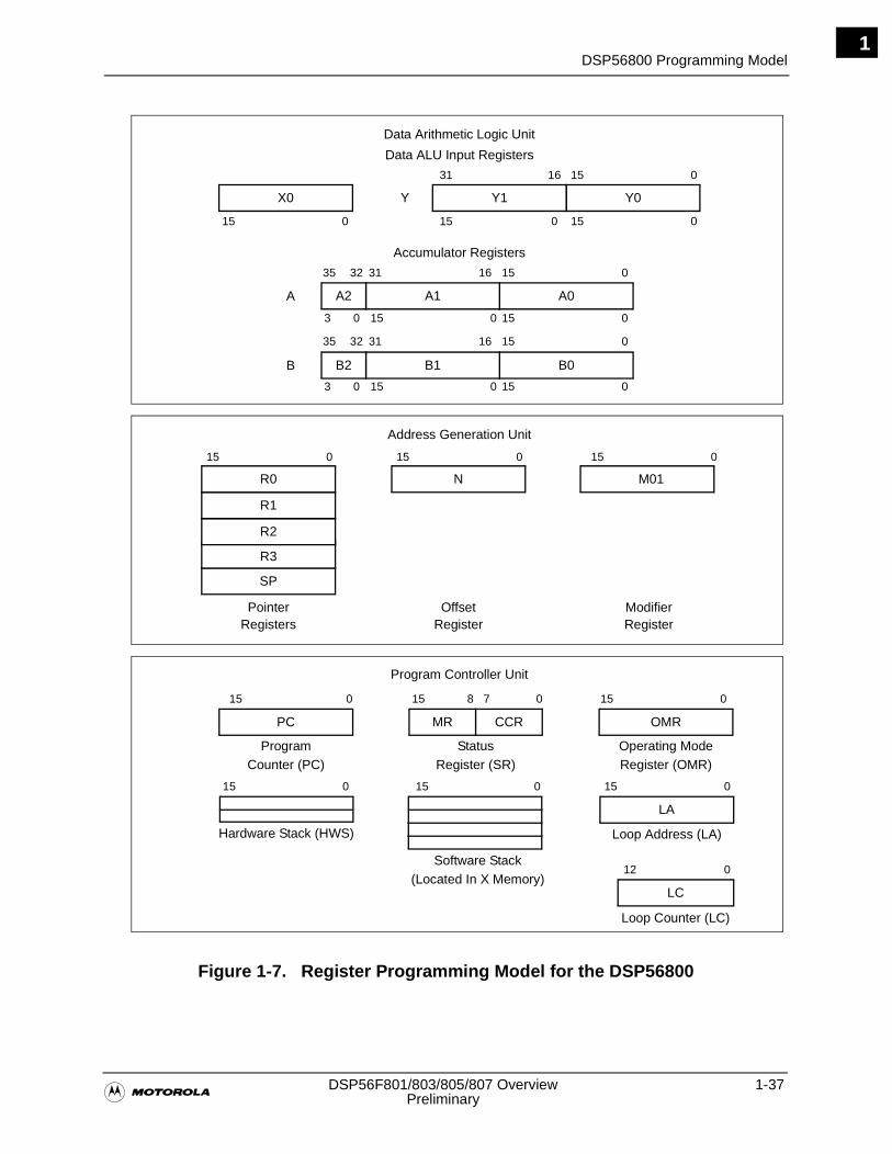
DSP56800 Programming Model
�DSP56F801/803/805/807 Overview 1-37
Preliminary
1
Figure 1-7. Register Programming Model for the DSP56800
N M01
Program Controller Unit
Hardware Stack (HWS)
Data ALU Input Registers
Accumulator Registers
Data Arithmetic Logic Unit
SP
R3
R2
R1
R0
MR CCR OMR
PointerRegisters
OffsetRegister
ModifierRegister
ProgramCounter (PC)
StatusRegister (SR)
Operating ModeRegister (OMR)
LA
LC
Loop Address (LA)
Loop Counter (LC)
Software Stack(Located In X Memory)
Y
A
B
X0 Y0Y1
A0A1A2
B0B1B2
PC
31 16 15 0
15 0 15 015 0
31 16 15 035 32
15 015 03
31 16 15 035 32
15 015 0
15 0 15 0 15 0
15 0 15 0 15 08 7
15 0 15 015 0
Address Generation Unit
12 0
0
3 0
1-38 DSP56F801/803/805/807 User’s Manual�Preliminary
DSP56800 Programming Model1

�Pin Descriptions 2-1
Preliminary
2
Chapter 2Pin Descriptions

2-2 DSP56F801/803/805/807 User’s Manual�Preliminary
2
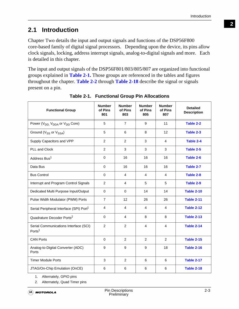
Introduction
�Pin Descriptions 2-3
Preliminary
22.1 Introduction
Chapter Two details the input and output signals and functions of the DSP56F800 core-based family of digital signal processors. Depending upon the device, its pins allow clock signals, locking, address interrupt signals, analog-to-digital signals and more. Each is detailed in this chapter.
The input and output signals of the DSP56F801/803/805/807 are organized into functional groups explained in Table 2-1. Those groups are referenced in the tables and figures throughout the chapter. Table 2-2 through Table 2-18 describe the signal or signals present on a pin.
Table 2-1. Functional Group Pin Allocations
Functional GroupNumber of Pins
801
Number of Pins
803
Number of Pins
805
Number of Pins
807
Detailed Description
Power (VDD, VDDA or VDD Core) 5 7 9 11 Table 2-2
Ground (VSS or VSSA) 5 6 8 12 Table 2-3
Supply Capacitors and VPP 2 2 3 4 Table 2-4
PLL and Clock 2 3 3 3 Table 2-5
Address Bus1 0 16 16 16 Table 2-6
Data Bus 0 16 16 16 Table 2-7
Bus Control 0 4 4 4 Table 2-8
Interrupt and Program Control Signals 2 4 5 5 Table 2-9
Dedicated Multi Purpose Input/Output 0 0 14 14 Table 2-10
Pulse Width Modulator (PWM) Ports 7 12 26 26 Table 2-11
Serial Peripheral Interface (SPI) Port1
1. Alternately, GPIO pins
4 4 4 4 Table 2-12
Quadrature Decoder Ports2
2. Alternately, Quad Timer pins
0 4 8 8 Table 2-13
Serial Communications Interface (SCI)
Ports12 2 4 4 Table 2-14
CAN Ports 0 2 2 2 Table 2-15
Analog-to-Digital Converter (ADC) Ports
9 9 9 18 Table 2-16
Timer Module Ports 3 2 6 6 Table 2-17
JTAG/On-Chip Emulation (OnCE) 6 6 6 6 Table 2-18
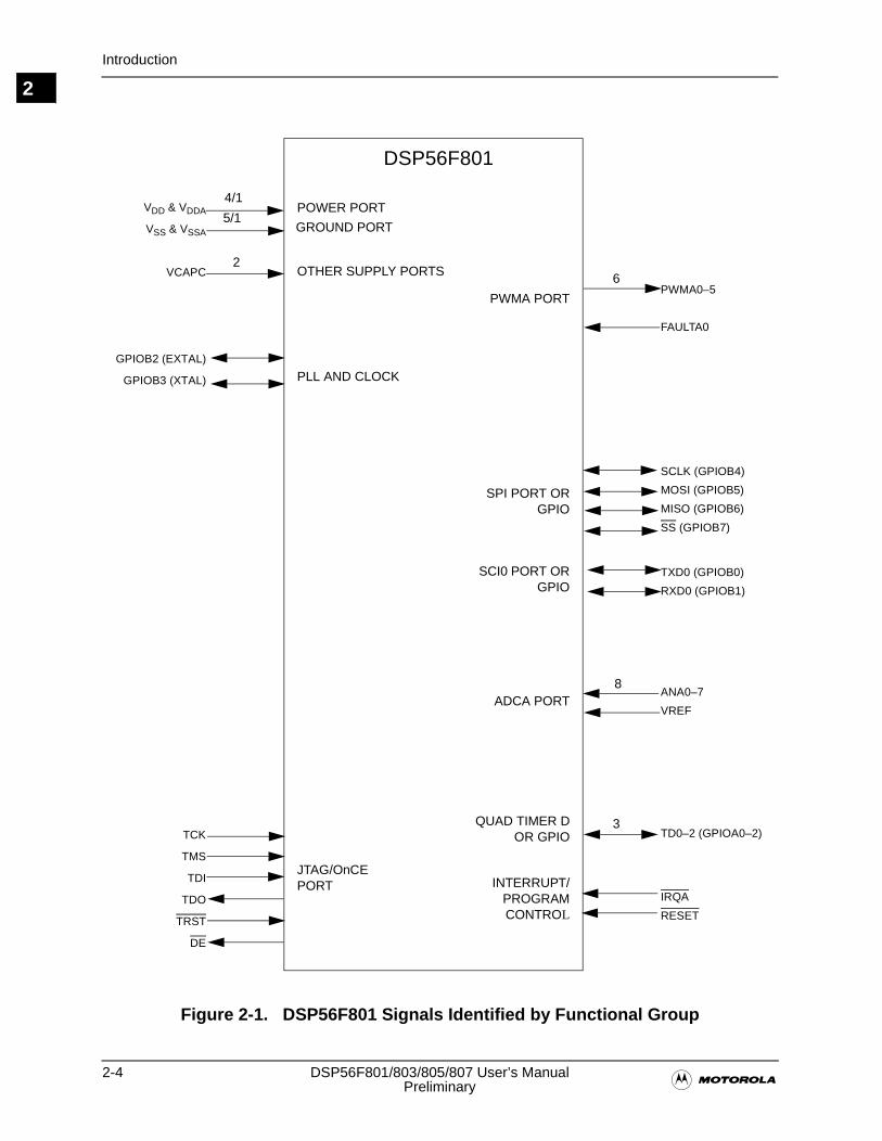
2-4 DSP56F801/803/805/807 User’s Manual�Preliminary
Introduction
2
Figure 2-1. DSP56F801 Signals Identified by Functional Group
DSP56F801
POWER PORT
GROUND PORT
OTHER SUPPLY PORTS
PLL AND CLOCK
PWMA PORT
SPI PORT ORGPIO
SCI0 PORT ORGPIO
VDD & VDDA
VSS & VSSA
VCAPC
GPIOB2 (EXTAL)
GPIOB3 (XTAL)
TCK
TMS
TDI
TDO
TRST
DE
ADCA PORT
JTAG/OnCE PORT
QUAD TIMER DOR GPIO
INTERRUPT/PROGRAMCONTROL
PWMA0–5
FAULTA0
SCLK (GPIOB4)
MOSI (GPIOB5)
MISO (GPIOB6)
SS (GPIOB7)
TXD0 (GPIOB0)
RXD0 (GPIOB1)
ANA0–7
VREF
TD0–2 (GPIOA0–2)
IRQA
RESET
4/1
5/1
26
8
3
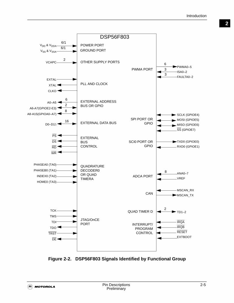
Introduction
�Pin Descriptions 2-5
Preliminary
2
Figure 2-2. DSP56F803 Signals Identified by Functional Group
DSP56F803
POWER PORT
GROUND PORT
OTHER SUPPLY PORTS
PLL AND CLOCK
EXTERNAL ADDRESS BUS OR GPIO
EXTERNAL DATA BUS
EXTERNAL BUS CONTROL
PWMA PORT
SPI PORT ORGPIO
SCI0 PORT ORGPIO
VDD & VDDA
VSS & VSSA
VCAPC
EXTAL
XTAL
CLKO
A0–A5
A6-A7(GPIOE2-E3)
A8-A15(GPIOA0–A7)
D0–D15
PS
DS
RD
WR
PHASEA0 (TA0)
PHASEB0 (TA1)
INDEX0 (TA2)
HOME0 (TA3)
TCK
TMS
TDI
TDO
TRST
DE
ADCA PORT
QUADRATURE DECODER0 OR QUAD TIMERA
JTAG/OnCE PORT
CAN
QUAD TIMER D
INTERRUPT/PROGRAMCONTROL
PWMA0–5
ISA0–2
FAULTA0–2
SCLK (GPIOE4)
MOSI (GPIOE5)
MISO (GPIOE6)
SS (GPIOE7)
TXD0 (GPIOE0)
RXD0 (GPIOE1)
ANA0–7
VREF
MSCAN_RX
MSCAN_TX
TD1–2
IRQA
IRQB
RESET
EXTBOOT
6/1
6/1
2
16
6
6
3
3
8
2
2
8
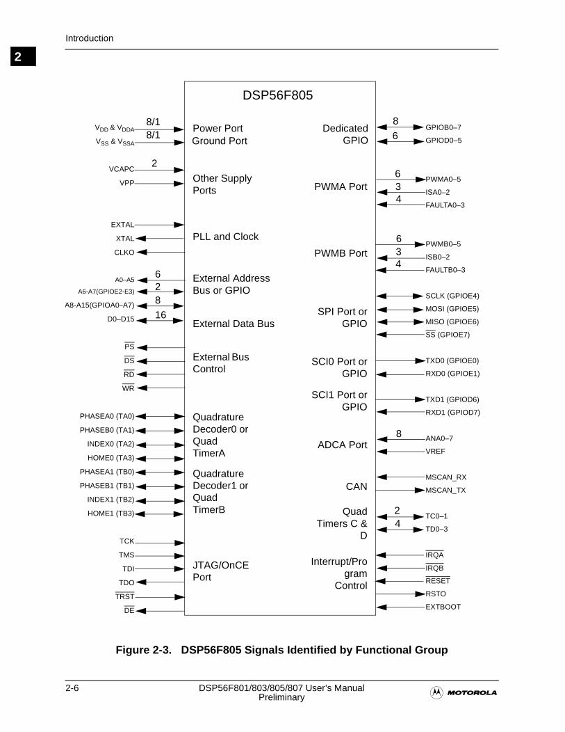
2-6 DSP56F801/803/805/807 User’s Manual�Preliminary
Introduction
2
Figure 2-3. DSP56F805 Signals Identified by Functional Group
DSP56F805
Power PortGround Port
Other Supply Ports
PLL and Clock
External Address Bus or GPIO
External Data Bus
External Bus Control
DedicatedGPIO
PWMA Port
PWMB Port
SPI Port orGPIO
SCI0 Port orGPIO
SCI1 Port orGPIO
VDD & VDDA
VSS & VSSA
VCAPC
VPP
EXTAL
XTAL
CLKO
A0–A5
A6-A7(GPIOE2-E3)
A8-A15(GPIOA0–A7)
D0–D15
PS
DS
RD
WR
PHASEA0 (TA0)
PHASEB0 (TA1)
INDEX0 (TA2)
HOME0 (TA3)
PHASEA1 (TB0)
PHASEB1 (TB1)
INDEX1 (TB2)
HOME1 (TB3)
TCK
TMS
TDI
TDO
TRST
DE
ADCA Port
Quadrature Decoder0 or Quad TimerA
Quadrature Decoder1 or Quad TimerB
JTAG/OnCE Port
CAN
QuadTimers C &
D
Interrupt/Program
Control
GPIOB0–7
GPIOD0–5
PWMA0–5
ISA0–2
FAULTA0–3
PWMB0–5
ISB0–2
FAULTB0–3
SCLK (GPIOE4)
MOSI (GPIOE5)
MISO (GPIOE6)
SS (GPIOE7)
TXD0 (GPIOE0)
RXD0 (GPIOE1)
TXD1 (GPIOD6)
RXD1 (GPIOD7)
ANA0–7
VREF
MSCAN_RX
MSCAN_TX
TC0–1
TD0–3
IRQA
IRQB
RESET
RSTO
EXTBOOT
8/18/1 6
2
16
6
8
634
634
8
24
28
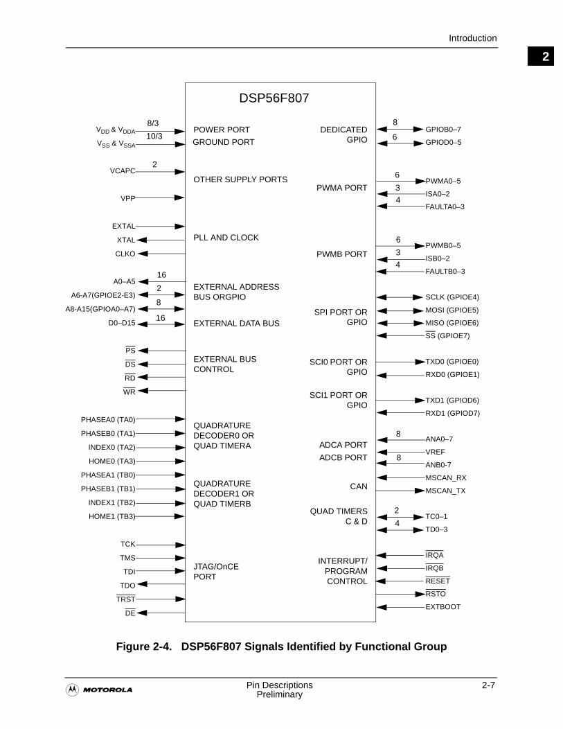
Introduction
�Pin Descriptions 2-7
Preliminary
2
Figure 2-4. DSP56F807 Signals Identified by Functional Group
DSP56F807
POWER PORT
GROUND PORT
OTHER SUPPLY PORTS
PLL AND CLOCK
EXTERNAL ADDRESS BUS ORGPIO
EXTERNAL DATA BUS
EXTERNAL BUS CONTROL
DEDICATEDGPIO
PWMA PORT
PWMB PORT
SPI PORT ORGPIO
SCI0 PORT ORGPIO
SCI1 PORT ORGPIO
VDD & VDDA
VSS & VSSA
VCAPC
VPP
EXTAL
XTAL
CLKO
A0–A5
A6-A7(GPIOE2-E3)
A8-A15(GPIOA0–A7)
D0–D15
PS
DS
RD
WR
PHASEA0 (TA0)
PHASEB0 (TA1)
INDEX0 (TA2)
HOME0 (TA3)
PHASEA1 (TB0)
PHASEB1 (TB1)
INDEX1 (TB2)
HOME1 (TB3)
TCK
TMS
TDI
TDO
TRST
DE
ADCA PORT
QUADRATURE DECODER0 OR QUAD TIMERA
QUADRATURE DECODER1 OR QUAD TIMERB
JTAG/OnCE PORT
CAN
QUAD TIMERSC & D
INTERRUPT/PROGRAMCONTROL
GPIOB0–7
GPIOD0–5
PWMA0–5
ISA0–2
FAULTA0–3
PWMB0–5
ISB0–2
FAULTB0–3
SCLK (GPIOE4)
MOSI (GPIOE5)
MISO (GPIOE6)
SS (GPIOE7)
TXD0 (GPIOE0)
RXD0 (GPIOE1)
TXD1 (GPIOD6)
RXD1 (GPIOD7)
ANA0–7
VREF
ANB0-7
MSCAN_RX
MSCAN_TX
TC0–1
TD0–3
IRQA
IRQB
RESET
RSTO
EXTBOOT
8/3
10/3 6
2
16
16
8
6
3
4
6
3
4
8
2
4
ADCB PORT 8
2
8
2-8 DSP56F801/803/805/807 User’s Manual�Preliminary
Power and Ground Signals
22.2 Power and Ground Signals
The following tables show power, ground, and bypass capacitor pinout data. Figures 2-5 through 2-8 show the physical layout of various grounds and voltage input signals associated with the Input/Output ring.
Table 2-2. Power Inputs
801 Pins
803 Pins
805 Pins
807 Pins
Signal Name
Signal Description
4 5 7 7 VDD Power—These pins provide power to the internal structures of the chip, and should all be attached to VDD.
1 2 2 4 VDDA Analog Power—These pins supply an analog power source.
Table 2-3. Grounds
801 Pins
803 Pins
805 Pins
807 Pins
Signal Name
Signal Description
4 5 7 9 VSS GND—These pins provide grounding for the internal structures of the chip, and should all be attached to VSS.
1 1 1 3 VSSA Analog Ground—This pin supplies an analog ground.
1 1 1 1 TCS TCS—This pin is reserved for factory use and must be tied to VSS for normal use. In block diagrams, this pin is considered an additional VSS.
Table 2-4. Supply Capacitors and VPP
801 Pins
803 Pins
805 Pins
807 Pins
Signal Name
SignalType
StateDuringReset
Signal Description
2 2 2 2 VCAPC Supply Supply VCAPC—Connect each pin to a 2.2µF bypass capacitor in order to bypass the core logic voltage regulator, required for proper chip operation.
N/A N/A 1 1 VPP Input Input VPP—This pin should be left unconnected as an open circuit for normal functionality.
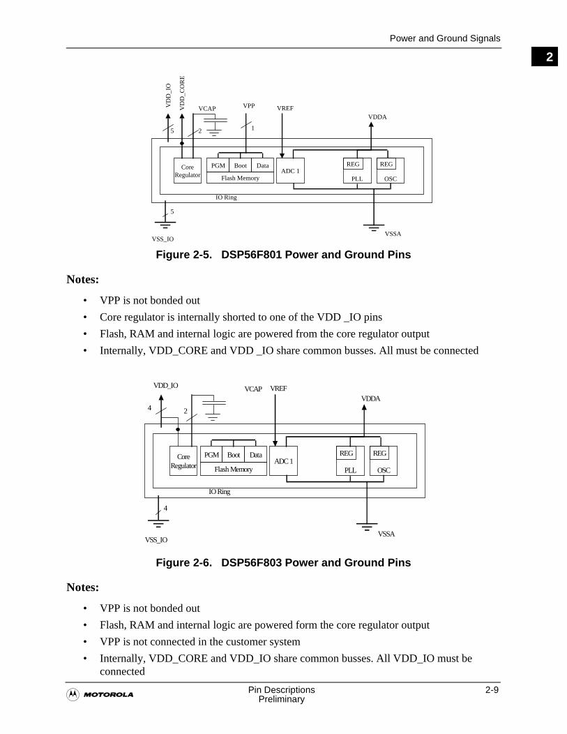
Power and Ground Signals
�Pin Descriptions 2-9
Preliminary
2
Figure 2-5. DSP56F801 Power and Ground Pins
Notes:
• VPP is not bonded out
• Core regulator is internally shorted to one of the VDD _IO pins
• Flash, RAM and internal logic are powered from the core regulator output
• Internally, VDD_CORE and VDD _IO share common busses. All must be connected
Figure 2-6. DSP56F803 Power and Ground Pins
Notes:
• VPP is not bonded out
• Flash, RAM and internal logic are powered form the core regulator output
• VPP is not connected in the customer system
• Internally, VDD_CORE and VDD_IO share common busses. All VDD_IO must be connected
ADC 1PLL
REG
OSC
REGV
DD
_IO
VSS_IO
IO Ring
VSSA
VDDAVREF
5
5
CoreRegulator
VCAP
Boot DataPGM
Flash Memory
VPP
12
VD
D_C
OR
E
CoreRegulator
ADC 1PLL
REG
OSC
REG
VDD_IO
VSS_IO
IO Ring
PGM Boot Data
Flash Memory
VCAP
VSSA
VDDAVREF
24
4
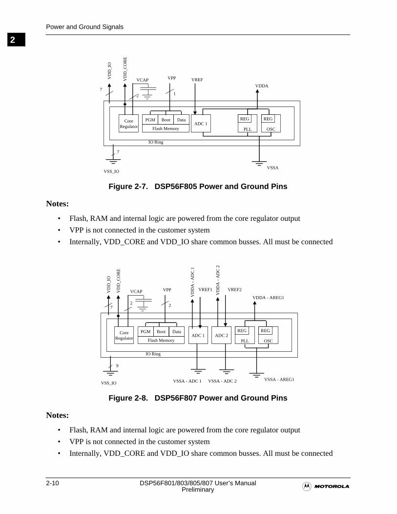
2-10 DSP56F801/803/805/807 User’s Manual�Preliminary
Power and Ground Signals
2
Figure 2-7. DSP56F805 Power and Ground Pins
Notes:
• Flash, RAM and internal logic are powered from the core regulator output
• VPP is not connected in the customer system
• Internally, VDD_CORE and VDD_IO share common busses. All must be connected
Figure 2-8. DSP56F807 Power and Ground Pins
Notes:
• Flash, RAM and internal logic are powered from the core regulator output
• VPP is not connected in the customer system
• Internally, VDD_CORE and VDD_IO share common busses. All must be connected
ADC 1PLL
REG
OSC
REG
VD
D_I
O
VSS_IO
IO Ring
VSSA
VDDAVREF
7
7
CoreRegulator
VCAP
Boot DataPGM
Flash Memory
VPP
12
VD
D_C
OR
E
ADC 1 ADC 2PLL
REG
OSC
REG
VD
D_I
O
VSS_IO
IO Ring
VSSA - ADC 1 VSSA - AREG1
VDDA - AREG1VD
DA
- A
DC
1
VREF1
VSSA - ADC 2
VD
DA
- A
DC
2
VREF2
PGM Boot Data
Flash Memory
VPP
227
9
CoreRegulator
VCAPVD
D_C
OR
E
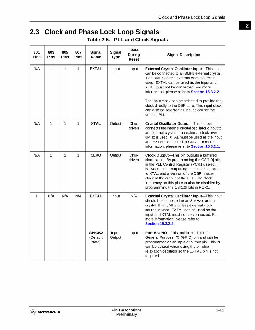
Clock and Phase Lock Loop Signals
�Pin Descriptions 2-11
Preliminary
22.3 Clock and Phase Lock Loop Signals
Table 2-5. PLL and Clock Signals
801 Pins
803 Pins
805 Pins
807 Pins
Signal Name
SignalType
StateDuringReset
Signal Description
N/A 1 1 1 EXTAL Input Input External Crystal Oscillator Input—This input can be connected to an 8MHz external crystal. If an 8MHz or less external clock source is used, EXTAL can be used as the input and XTAL must not be connected. For more information, please refer to Section 15.3.2.2.
The input clock can be selected to provide the clock directly to the DSP core. This input clock can also be selected as input clock for the on-chip PLL.
N/A 1 1 1 XTAL Output Chip-driven
Crystal Oscillator Output—This output connects the internal crystal oscillator output to an external crystal. If an external clock over 8MHz is used, XTAL must be used as the input and EXTAL connected to GND. For more information, please refer to Section 15.3.2.1.
N/A 1 1 1 CLKO Output Chip-driven
Clock Output—This pin outputs a buffered clock signal. By programming the CS[1:0] bits in the PLL Control Register (PCR1), select between either outputting of the signal applied to XTAL and a version of the DSP master clock at the output of the PLL. The clock frequency on this pin can also be disabled by programming the CS[1:0] bits in PCR1.
1 N/A N/A N/A EXTAL
GPIOB2(Default state)
Input
Input/ Output
N/A
Input
External Crystal Oscillator Input—This input should be connected to an 8 MHz external crystal. If an 8MHz or less external clock source is used, EXTAL can be used as the input and XTAL must not be connected. For more information, please refer to Section 15.3.2.2.
Port B GPIO—This multiplexed pin is a General Purpose I/O (GPIO) pin and can be programmed as an input or output pin. This I/O can be utilized when using the on-chip relaxation oscillator so the EXTAL pin is not required.
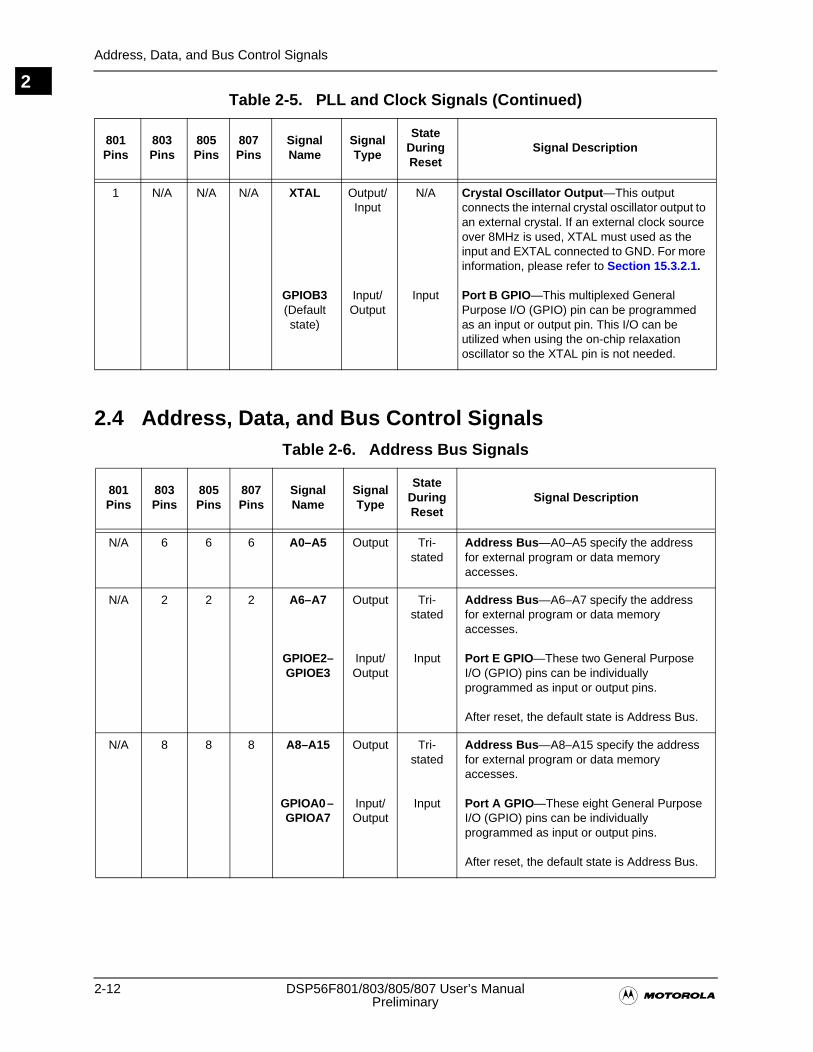
2-12 DSP56F801/803/805/807 User’s Manual�Preliminary
Address, Data, and Bus Control Signals
2
2.4 Address, Data, and Bus Control Signals
1 N/A N/A N/A XTAL
GPIOB3(Default state)
Output/Input
Input/ Output
N/A
Input
Crystal Oscillator Output—This output connects the internal crystal oscillator output to an external crystal. If an external clock source over 8MHz is used, XTAL must used as the input and EXTAL connected to GND. For more information, please refer to Section 15.3.2.1.
Port B GPIO—This multiplexed General Purpose I/O (GPIO) pin can be programmed as an input or output pin. This I/O can be utilized when using the on-chip relaxation oscillator so the XTAL pin is not needed.
Table 2-6. Address Bus Signals
801 Pins
803 Pins
805 Pins
807 Pins
SignalName
SignalType
State During Reset
Signal Description
N/A 6 6 6 A0–A5 Output Tri-stated
Address Bus —A0–A5 specify the address for external program or data memory accesses.
N/A 2 2 2 A6–A7
GPIOE2–GPIOE3
Output
Input/Output
Tri-stated
Input
Address Bus —A6–A7 specify the address for external program or data memory accesses.
Port E GPIO—These two General Purpose I/O (GPIO) pins can be individually programmed as input or output pins.
After reset, the default state is Address Bus.
N/A 8 8 8 A8–A15
GPIOA0 – GPIOA7
Output
Input/Output
Tri-stated
Input
Address Bus —A8–A15 specify the address for external program or data memory accesses.
Port A GPIO—These eight General Purpose I/O (GPIO) pins can be individually programmed as input or output pins.
After reset, the default state is Address Bus.
Table 2-5. PLL and Clock Signals (Continued)
801 Pins
803 Pins
805 Pins
807 Pins
Signal Name
SignalType
StateDuringReset
Signal Description
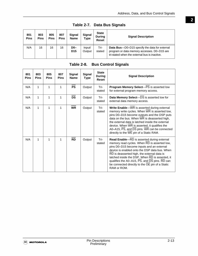
Address, Data, and Bus Control Signals
�Pin Descriptions 2-13
Preliminary
2Table 2-7. Data Bus Signals
801 Pins
803 Pins
805 Pins
807 Pins
SignalName
Signal Type
State During Reset
Signal Description
N/A 16 16 16 D0–D15
Input/Output
Tri-stated
Data Bus —D0–D15 specify the data for external program or data memory accesses. D0–D15 are tri-stated when the external bus is inactive.
Table 2-8. Bus Control Signals
801 Pins
803 Pins
805 Pins
807 Pins
SignalName
SignalType
State During Reset
Signal Description
N/A 1 1 1 PS Output Tri-stated
Program Memory Select—PS is asserted low for external program memory access.
N/A 1 1 1 DS Output Tri-stated
Data Memory Select—DS is asserted low for external data memory access.
N/A 1 1 1 WR Output Tri-stated
Write Enable—WR is asserted during external memory write cycles. When WR is asserted low, pins D0–D15 become outputs and the DSP puts data on the bus. When WR is deasserted high, the external data is latched inside the external device. When WR is asserted, it qualifies the A0–A15, PS, and DS pins. WR can be connected directly to the WE pin of a Static RAM.
N/A 1 1 1 RD Output Tri-stated
Read Enable—RD is asserted during external memory read cycles. When RD is asserted low, pins D0–D15 become inputs and an external device is enabled onto the DSP data bus. When RD is deasserted high, the external data is latched inside the DSP. When RD is asserted, it qualifies the A0–A15, PS, and DS pins. RD can be connected directly to the OE pin of a Static RAM or ROM.
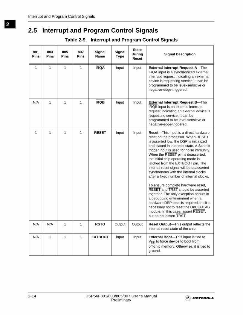
2-14 DSP56F801/803/805/807 User’s Manual�Preliminary
Interrupt and Program Control Signals
22.5 Interrupt and Program Control Signals
Table 2-9. Interrupt and Program Control Signals
801 Pins
803 Pins
805 Pins
807 Pins
Signal Name
SignalType
StateDuringReset
Signal Description
1 1 1 1 IRQA Input Input External Interrupt Request A—The IRQA input is a synchronized external interrupt request indicating an external device is requesting service. It can be programmed to be level-sensitive or negative-edge-triggered.
N/A 1 1 1 IRQB Input Input External Interrupt Request B—The IRQB input is an external interrupt request indicating an external device is requesting service. It can be programmed to be level-sensitive or negative-edge-triggered.
1 1 1 1 RESET Input Input Reset—This input is a direct hardware reset on the processor. When RESET is asserted low, the DSP is initialized and placed in the reset state. A Schmitt trigger input is used for noise immunity. When the RESET pin is deasserted, the initial chip operating mode is latched from the EXTBOOT pin. The internal reset signal will be deasserted synchronous with the internal clocks after a fixed number of internal clocks.
To ensure complete hardware reset, RESET and TRST should be asserted together. The only exception occurs in a debugging environment when a hardware DSP reset is required and it is necessary not to reset the OnCE/JTAG module. In this case, assert RESET, but do not assert TRST.
N/A N/A 1 1 RSTO Output Output Reset Output—This output reflects the internal reset state of the chip.
N/A 1 1 1 EXTBOOT Input Input External Boot—This input is tied to VDD to force device to boot from off-chip memory. Otherwise, it is tied to ground.
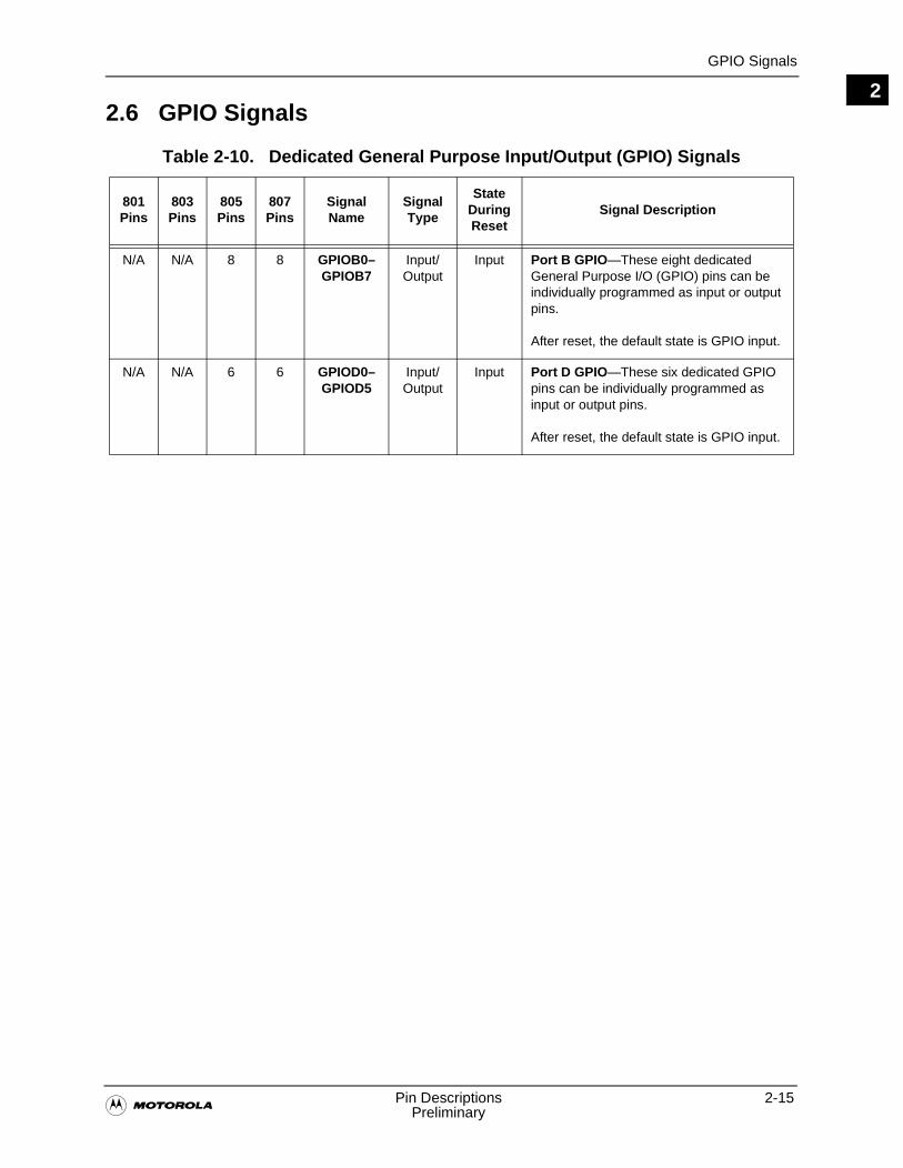
GPIO Signals
�Pin Descriptions 2-15
Preliminary
22.6 GPIO Signals
Table 2-10. Dedicated General Purpose Input/Output (GPIO) Signals
801 Pins
803 Pins
805 Pins
807 Pins
SignalName
SignalType
State During Reset
Signal Description
N/A N/A 8 8 GPIOB0–GPIOB7
Input/Output
Input Port B GPIO —These eight dedicated General Purpose I/O (GPIO) pins can be individually programmed as input or output pins.
After reset, the default state is GPIO input.
N/A N/A 6 6 GPIOD0–GPIOD5
Input/Output
Input Port D GPIO —These six dedicated GPIO pins can be individually programmed as input or output pins.
After reset, the default state is GPIO input.
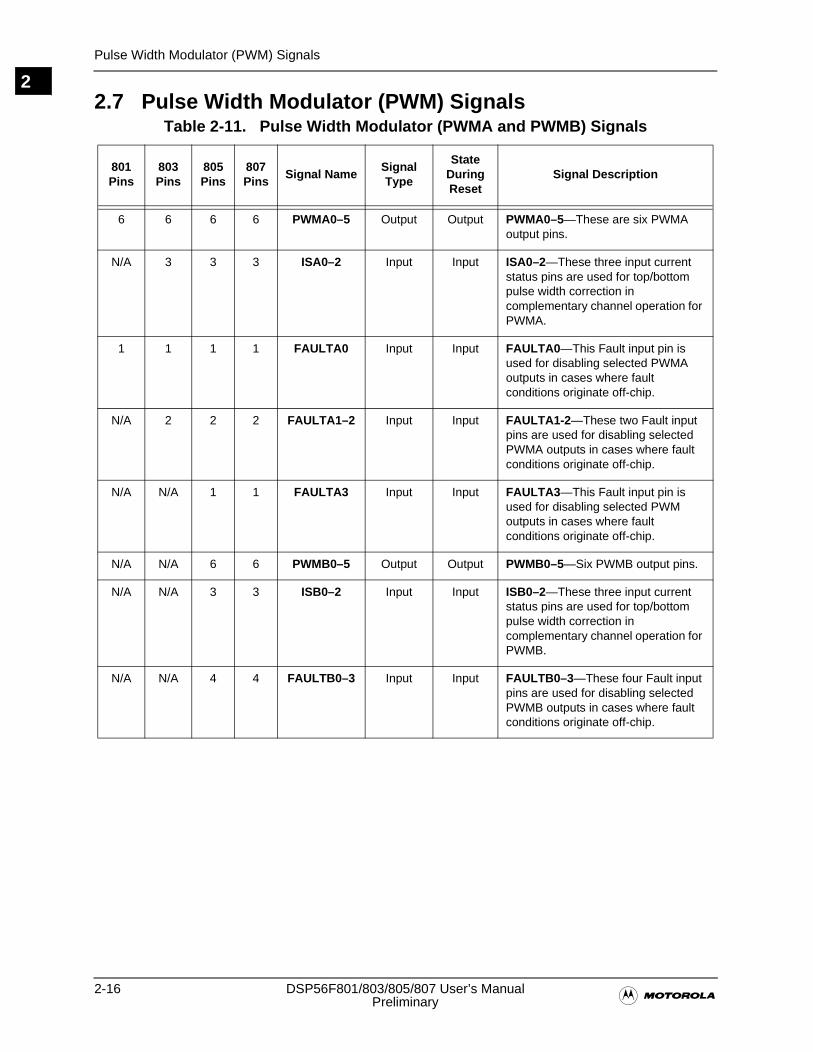
2-16 DSP56F801/803/805/807 User’s Manual�Preliminary
Pulse Width Modulator (PWM) Signals
22.7 Pulse Width Modulator (PWM) Signals
Table 2-11. Pulse Width Modulator (PWMA and PWMB) Signals
801 Pins
803 Pins
805 Pins
807 Pins
Signal NameSignalType
State During Reset
Signal Description
6 6 6 6 PWMA0–5 Output Output PWMA0–5—These are six PWMA output pins.
N/A 3 3 3 ISA0–2 Input Input ISA0–2—These three input current status pins are used for top/bottom pulse width correction in complementary channel operation for PWMA.
1 1 1 1 FAULTA0 Input Input FAULTA0—This Fault input pin is used for disabling selected PWMA outputs in cases where fault conditions originate off-chip.
N/A 2 2 2 FAULTA1–2 Input Input FAULTA1-2 —These two Fault input pins are used for disabling selected PWMA outputs in cases where fault conditions originate off-chip.
N/A N/A 1 1 FAULTA3 Input Input FAULTA3—This Fault input pin is used for disabling selected PWM outputs in cases where fault conditions originate off-chip.
N/A N/A 6 6 PWMB0–5 Output Output PWMB0–5—Six PWMB output pins.
N/A N/A 3 3 ISB0–2 Input Input ISB0–2—These three input current status pins are used for top/bottom pulse width correction in complementary channel operation for PWMB.
N/A N/A 4 4 FAULTB0–3 Input Input FAULTB0–3 —These four Fault input pins are used for disabling selected PWMB outputs in cases where fault conditions originate off-chip.
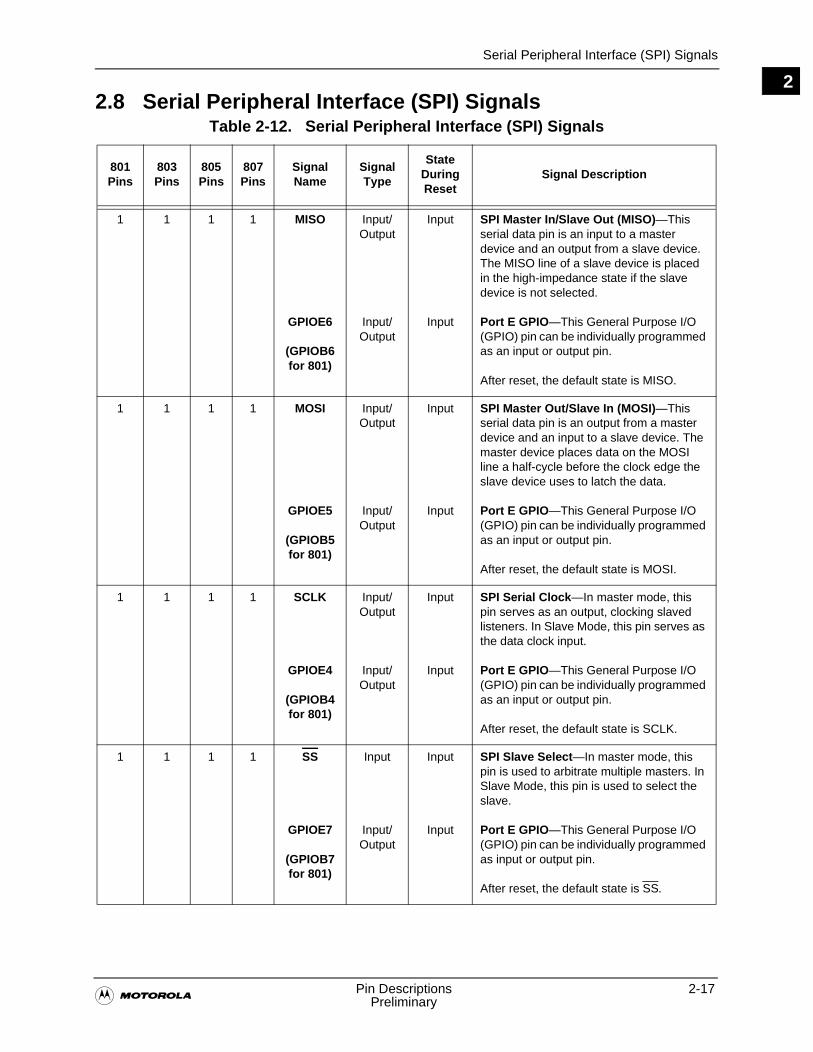
Serial Peripheral Interface (SPI) Signals
�Pin Descriptions 2-17
Preliminary
22.8 Serial Peripheral Interface (SPI) Signals
Table 2-12. Serial Peripheral Interface (SPI) Signals
801 Pins
803 Pins
805 Pins
807 Pins
Signal Name
SignalType
State During Reset
Signal Description
1 1 1 1 MISO
GPIOE6
(GPIOB6 for 801)
Input/Output
Input/Output
Input
Input
SPI Master In/Slave Out (MISO)—This serial data pin is an input to a master device and an output from a slave device. The MISO line of a slave device is placed in the high-impedance state if the slave device is not selected.
Port E GPIO—This General Purpose I/O (GPIO) pin can be individually programmed as an input or output pin.
After reset, the default state is MISO.
1 1 1 1 MOSI
GPIOE5
(GPIOB5 for 801)
Input/Output
Input/Output
Input
Input
SPI Master Out/Slave In (MOSI)—This serial data pin is an output from a master device and an input to a slave device. The master device places data on the MOSI line a half-cycle before the clock edge the slave device uses to latch the data.
Port E GPIO—This General Purpose I/O (GPIO) pin can be individually programmed as an input or output pin.
After reset, the default state is MOSI.
1 1 1 1 SCLK
GPIOE4
(GPIOB4 for 801)
Input/Output
Input/Output
Input
Input
SPI Serial Clock—In master mode, this pin serves as an output, clocking slaved listeners. In Slave Mode, this pin serves as the data clock input.
Port E GPIO—This General Purpose I/O (GPIO) pin can be individually programmed as an input or output pin.
After reset, the default state is SCLK.
1 1 1 1 SS
GPIOE7
(GPIOB7 for 801)
Input
Input/Output
Input
Input
SPI Slave Select—In master mode, this pin is used to arbitrate multiple masters. In Slave Mode, this pin is used to select the slave.
Port E GPIO—This General Purpose I/O (GPIO) pin can be individually programmed as input or output pin.
After reset, the default state is SS.
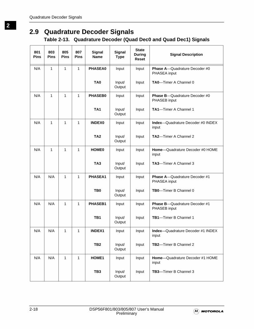
2-18 DSP56F801/803/805/807 User’s Manual�Preliminary
Quadrature Decoder Signals
22.9 Quadrature Decoder Signals
Table 2-13. Quadrature Decoder (Quad Dec0 and Quad Dec1) Signals
801 Pins
803 Pins
805 Pins
807 Pins
Signal Name
SignalType
State During Reset
Signal Description
N/A 1 1 1 PHASEA0
TA0
Input
Input/Output
Input
Input
Phase A—Quadrature Decoder #0 PHASEA input
TA0—Timer A Channel 0
N/A 1 1 1 PHASEB0
TA1
Input
Input/Output
Input
Input
Phase B—Quadrature Decoder #0 PHASEB input
TA1—Timer A Channel 1
N/A 1 1 1 INDEX0
TA2
Input
Input/Output
Input
Input
Index—Quadrature Decoder #0 INDEX input
TA2—Timer A Channel 2
N/A 1 1 1 HOME0
TA3
Input
Input/Output
Input
Input
Home—Quadrature Decoder #0 HOME input
TA3—Timer A Channel 3
N/A N/A 1 1 PHASEA1
TB0
Input
Input/Output
Input
Input
Phase A—Quadrature Decoder #1 PHASEA input
TB0—Timer B Channel 0
N/A N/A 1 1 PHASEB1
TB1
Input
Input/Output
Input
Input
Phase B—Quadrature Decoder #1 PHASEB input
TB1—Timer B Channel 1
N/A N/A 1 1 INDEX1
TB2
Input
Input/Output
Input
Input
Index—Quadrature Decoder #1 INDEX input
TB2—Timer B Channel 2
N/A N/A 1 1 HOME1
TB3
Input
Input/Output
Input
Input
Home—Quadrature Decoder #1 HOME input
TB3—Timer B Channel 3
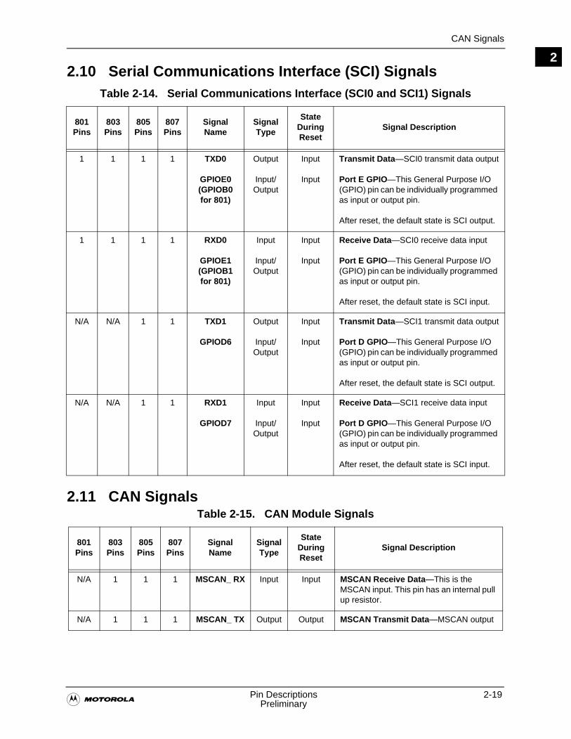
CAN Signals
�Pin Descriptions 2-19
Preliminary
22.10 Serial Communications Interface (SCI) Signals
2.11 CAN Signals
Table 2-14. Serial Communications Interface (SCI0 and SCI1) Signals
801 Pins
803 Pins
805 Pins
807 Pins
Signal Name
SignalType
State During Reset
Signal Description
1 1 1 1 TXD0
GPIOE0(GPIOB0 for 801)
Output
Input/Output
Input
Input
Transmit Data—SCI0 transmit data output
Port E GPIO—This General Purpose I/O (GPIO) pin can be individually programmed as input or output pin.
After reset, the default state is SCI output.
1 1 1 1 RXD0
GPIOE1(GPIOB1 for 801)
Input
Input/Output
Input
Input
Receive Data—SCI0 receive data input
Port E GPIO—This General Purpose I/O (GPIO) pin can be individually programmed as input or output pin.
After reset, the default state is SCI input.
N/A N/A 1 1 TXD1
GPIOD6
Output
Input/Output
Input
Input
Transmit Data—SCI1 transmit data output
Port D GPIO—This General Purpose I/O (GPIO) pin can be individually programmed as input or output pin.
After reset, the default state is SCI output.
N/A N/A 1 1 RXD1
GPIOD7
Input
Input/Output
Input
Input
Receive Data—SCI1 receive data input
Port D GPIO—This General Purpose I/O (GPIO) pin can be individually programmed as input or output pin.
After reset, the default state is SCI input.
Table 2-15. CAN Module Signals
801 Pins
803 Pins
805 Pins
807 Pins
SignalName
Signal Type
State During Reset
Signal Description
N/A 1 1 1 MSCAN_ RX Input Input MSCAN Receive Data—This is the MSCAN input. This pin has an internal pull up resistor.
N/A 1 1 1 MSCAN_ TX Output Output MSCAN Transmit Data—MSCAN output
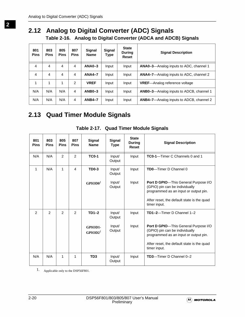
2-20 DSP56F801/803/805/807 User’s Manual�Preliminary
Analog to Digital Converter (ADC) Signals
22.12 Analog to Digital Converter (ADC) Signals
2.13 Quad Timer Module Signals
Table 2-16. Analog to Digital Converter (ADCA and ADCB) Signals
801 Pins
803 Pins
805 Pins
807 Pins
SignalName
Signal Type
State During Reset
Signal Description
4 4 4 4 ANA0–3 Input Input ANA0–3—Analog inputs to ADC, channel 1
4 4 4 4 ANA4–7 Input Input ANA4–7—Analog inputs to ADC, channel 2
1 1 1 2 VREF Input Input VREF—Analog reference voltage
N/A N/A N/A 4 ANB0–3 Input Input ANB0–3—Analog inputs to ADCB, channel 1
N/A N/A N/A 4 ANB4–7 Input Input ANB4–7—Analog inputs to ADCB, channel 2
Table 2-17. Quad Timer Module Signals
801 Pins
803 Pins
805 Pins
807 Pins
SignalName
Signal Type
State During Reset
Signal Description
N/A N/A 2 2 TC0-1 Input/Output
Input TC0-1—Timer C Channels 0 and 1
1 N/A 1 4 TD0-3
GPIOD01
Input/Output
Input/Output
Input
Input
TD0—Timer D Channel 0
Port D GPIO—This General Purpose I/O (GPIO) pin can be individually programmed as an input or output pin.
After reset, the default state is the quad timer input.
2 2 2 2 TD1–2
GPIOD1-
GPIOD21
1. Applicable only to the DSP56F801.
Input/ Output
Input/ Output
Input
Input
TD1–2—Timer D Channel 1–2
Port D GPIO—This General Purpose I/O (GPIO) pin can be individually programmed as an input or output pin.
After reset, the default state is the quad timer input.
N/A N/A 1 1 TD3 Input/ Output
Input TD3—Timer D Channel 0–2
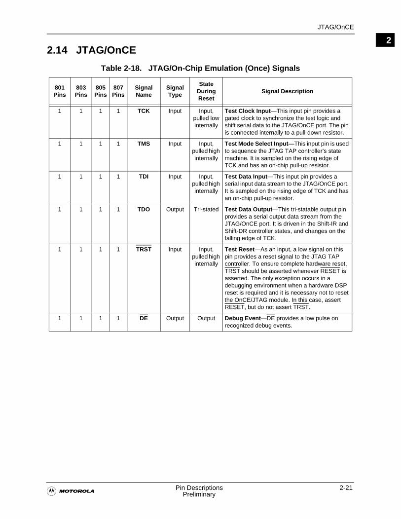
JTAG/OnCE
�Pin Descriptions 2-21
Preliminary
22.14 JTAG/OnCE
Table 2-18. JTAG/On-Chip Emulation (Once) Signals
801 Pins
803 Pins
805 Pins
807 Pins
Signal Name
Signal Type
State During Reset
Signal Description
1 1 1 1 TCK Input Input, pulled low internally
Test Clock Input—This input pin provides a gated clock to synchronize the test logic and shift serial data to the JTAG/OnCE port. The pin is connected internally to a pull-down resistor.
1 1 1 1 TMS Input Input, pulled high internally
Test Mode Select Input—This input pin is used to sequence the JTAG TAP controller’s state machine. It is sampled on the rising edge of TCK and has an on-chip pull-up resistor.
1 1 1 1 TDI Input Input, pulled high internally
Test Data Input—This input pin provides a serial input data stream to the JTAG/OnCE port. It is sampled on the rising edge of TCK and has an on-chip pull-up resistor.
1 1 1 1 TDO Output Tri-stated Test Data Output—This tri-statable output pin provides a serial output data stream from the JTAG/OnCE port. It is driven in the Shift-IR and Shift-DR controller states, and changes on the falling edge of TCK.
1 1 1 1 TRST Input Input, pulled high internally
Test Reset—As an input, a low signal on this pin provides a reset signal to the JTAG TAP controller. To ensure complete hardware reset, TRST should be asserted whenever RESET is asserted. The only exception occurs in a debugging environment when a hardware DSP reset is required and it is necessary not to reset the OnCE/JTAG module. In this case, assert RESET, but do not assert TRST.
1 1 1 1 DE Output Output Debug Event—DE provides a low pulse on recognized debug events.

2-22 DSP56F801/803/805/807 User’s Manual�Preliminary
JTAG/OnCE
2
�Memory and Operating Modes 3-1
Preliminary
3
Chapter 3Memory and Operating Modes

3-2 DSP56F801/803/805/807 User’s Manual�Preliminary
3
DSP56F801/803/805/807 Memory Map Description
�Memory and Operating Modes 3-3
Preliminary
33.1 Memory Map
The DSP56F800 family is very adaptable. A complete controller on a single, high-performance chip with flash technology and analog-to-digital converters embedded on a single mechanism. This section describes detailed, on-chip memories and the opening modes of the DSP56F800 core-based chip family. Additionally, interrupt vectors, Interrupt Priority Register (IPR) and peripheral memory maps are also located in this chapter.
3.2 DSP56F801/803/805/807 Memory Map Description
The DSP56F801/803/805/807 uses two independent memory spaces, data and program, using a Harvard architecture. RAM and Flash memory are used for the on-chip data memory and for the on-chip program memory.
Table 3-1. Chip Memory Configurations
On-chip memory sizes for each of the parts are summarized in Table 3-1. Both the program and data memories can be expanded off-chip. The program memory map is located in Table 3-2. The operating mode control bits (MA and MB) in the Operating Mode Register (OMR), coupled with the BOOTMAP_B bit in the SYS_CNTL register, see Section 16.7.1 System Control Register (SYS_CNTL), control the program memory map and select the vector address.
The DSP56F803, DSP56F805, and DSP56F807 chips include external memory expansion capabilities up to 64K words. This is not available on the DSP56F801chip.
On-Chip Memory DSP56F801 DSP56F803 DSP56F805 DSP56F807
Program Flash (PFLASH) 8K x 16 32252 x 16 32252 x 16 60K x 16
Data Flash (XFLASH) 2K x 16 4K x 16 4K x 16 8K x 16
Program RAM (PRAM) 1K x 16 512 x 16 512 x 16 2K x 16
Data RAM (XRAM) 1K x 16 2K x 16 2K x 16 4K x 16
Program Boot Flash 2K x 16
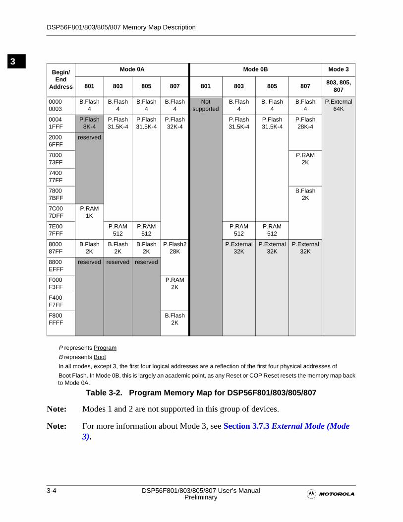
3-4 DSP56F801/803/805/807 User’s Manual�Preliminary
DSP56F801/803/805/807 Memory Map Description
3
P represents Program
B represents Boot
In all modes, except 3, the first four logical addresses are a reflection of the first four physical addresses of
Boot Flash. In Mode 0B, this is largely an academic point, as any Reset or COP Reset resets the memory map backto Mode 0A.
Table 3-2. Program Memory Map for DSP56F801/803/805/807
Note: Modes 1 and 2 are not supported in this group of devices.
Note: For more information about Mode 3, see Section 3.7.3 External Mode (Mode 3).
Begin/ End
Address
Mode 0A Mode 0B Mode 3
801 803 805 807 801 803 805 807803, 805,
807
00000003
B.Flash 4
B.Flash 4
B.Flash 4
B.Flash 4
Not supported
B.Flash 4
B. Flash 4
B.Flash4
P.External 64K
00041FFF
P.Flash 8K-4
P.Flash 31.5K-4
P.Flash 31.5K-4
P.Flash 32K-4
P.Flash 31.5K-4
P.Flash 31.5K-4
P.Flash 28K-4
20006FFF
reserved
700073FF
P.RAM 2K
740077FF
78007BFF
B.Flash 2K
7C007DFF
P.RAM 1K
7E007FFF
P.RAM 512
P.RAM 512
P.RAM 512
P.RAM 512
800087FF
B.Flash 2K
B.Flash 2K
B.Flash 2K
P.Flash2 28K
P.External 32K
P.External 32K
P.External 32K
8800EFFF
reserved reserved reserved
F000F3FF
P.RAM 2K
F400F7FF
F800FFFF
B.Flash 2K
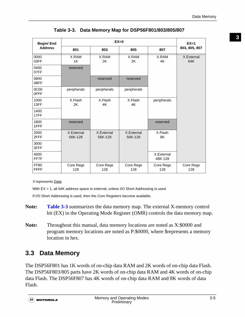
Data Memory
�Memory and Operating Modes 3-5
Preliminary
3Table 3-3. Data Memory Map for DSP56F801/803/805/807
X represents Data
With EX = 1, all 64K address space is external, unless I/O Short Addressing is used.
If I/O Short Addressing is used, then the Core Registers become available.
Note: Table 3-3 summarizes the data memory map. The external X-memory control bit (EX) in the Operating Mode Register (OMR) controls the data memory map.
Note: Throughout this manual, data memory locations are noted as X:$0000 and program memory locations are noted as P:$0000, where $represents a memory location in hex.
3.3 Data Memory
The DSP56F801 has 1K words of on-chip data RAM and 2K words of on-chip data Flash. The DSP56F803/805 parts have 2K words of on-chip data RAM and 4K words of on-chip data Flash. The DSP56F807 has 4K words of on-chip data RAM and 8K words of data Flash.
Begin/ End Address
EX=0 EX=1803, 805, 807801 803 805 807
0000 03FF
X.RAM 1K
X.RAM 2K
X.RAM 2K
X.RAM 4K
X.External 64K
0400 07FF
reserved
08000BFF
reserved reserved
0C00 0FFF
peripherals peripherals peripherals
1000 13FF
X.Flash 2K
X.Flash 4K
X.Flash 4K
peripherals
1400 17FF
1800 1FFF
reserved reserved
2000 2FFF
X.External 56K-128
X.External 56K-128
X.External 56K-128
X.Flash 8K
3000 3FFF
4000 FF7F
X.External 48K-128
FF80 FFFF
Core Regs 128
Core Regs 128
Core Regs 128
Core Regs 128
Core Regs 128
3-6 DSP56F801/803/805/807 User’s Manual�Preliminary
Data Memory
3The 128 data memory addresses at the top of the memory map ($FF80 to $FFFF) are reserved for DSP56800 on-chip core configuration registers. Additionally, there is a 1K word, $0800 to $0BFF, a non-accessible segment hole in the memory map in the 803 and 805. The 801 has a 2K hole while the 807 has no hole. No memory location will be selected on attempted accesses to the hole when EX = 0, internal data memory map enabled. When EX = 1, the hole does not exist and may be accessed like all other external data memory.
Note: For DSP56800 core instructions performing two reads from the data memory in a single instruction, the second access using the R3 pointer always occurs to on-chip memory, regardless of how the OMR’s EX bit is programmed. For example, the second read of the following code sequence accesses on-chip X data memory X:$0:
MOVE #$0000,R3
NOP
MOVE X:(R1)+,Y0 X:(R3)+,X0
The data memory may be expanded off-chip for the DSP56F803/805/807 but not for the DSP56F801. When the OMR’s EX bit is programmed with a one, there are 65,536 addressable off-chip data memory locations.
When the EX bit is set, the on-chip core configuration registers may only be accessed using the I/O short addressing mode.
The external data memory bus access time is controlled by four bits of the Bus Control Register (BCR) located at X:$FFF9. This register is shown in Figure 3-1.
The External X bit (EX, bit 3) of the OMR in the DSP56800 core determines the mapping of the data memory, as shown in Table 3-3. Setting the EX bit to 1 completely disables the on-chip data memory and enables a full 64K external data memory map.
Note: Two exceptions to this rule exist. The first exception is, if a MOVE, TSTW, or BIT FIELD instruction is used with the I/O Short Addressing Mode, the EX bit is ignored. This allows the on-chip core control registers to be accessed when the EX bit is set. When the EX bit is set, the access time to any external data memory is controlled by the BCR. The second exception is for instructions performing two reads from the data memory in a single cycle, the EX bit is ignored during the second access using the R3 pointer.
A complete description of the Operating Mode Register (OMR) is provided in DSP56800 Family Manual (DSP56800FAM/AD).
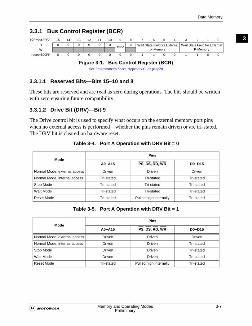
Data Memory
�Memory and Operating Modes 3-7
Preliminary
33.3.1 Bus Control Register (BCR)
Figure 3-1. Bus Control Register (BCR)See Programmer’s Sheet, Appendix C, on page20
3.3.1.1 Reserved Bits—Bits 15–10 and 8
These bits are reserved and are read as zero during operations. The bits should be written with zero ensuring future compatibility.
3.3.1.2 Drive Bit (DRV)—Bit 9
The Drive control bit is used to specify what occurs on the external memory port pins when no external access is performed—whether the pins remain driven or are tri-stated. The DRV bit is cleared on hardware reset.
Table 3-4. Port A Operation with DRV Bit = 0
Table 3-5. Port A Operation with DRV Bit = 1
BCR–X:$FFF9 15 14 13 12 11 10 9 8 7 6 5 4 3 2 1 0
R 0 0 0 0 0 0DRV
0 Wait State Field for External X-Memory
Wait State Field for External P-MemoryW
reset=$00FF 0 0 0 0 0 0 0 0 1 1 0 0 1 1 0 0
ModePins
A0–A15 PS, DS, RD, WR D0–D15
Normal Mode, external access Driven Driven Driven
Normal Mode, internal access Tri-stated Tri-stated Tri-stated
Stop Mode Tri-stated Tri-stated Tri-stated
Wait Mode Tri-stated Tri-stated Tri-stated
Reset Mode Tri-stated Pulled high internally Tri-stated
ModePins
A0–A15 PS, DS, RD, WR D0–D15
Normal Mode, external access Driven Driven Driven
Normal Mode, internal access Driven Driven Tri-stated
Stop Mode Driven Driven Tri-stated
Wait Mode Driven Driven Tri-stated
Reset Mode Tri-stated Pulled high internally Tri-stated
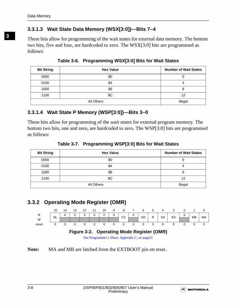
3-8 DSP56F801/803/805/807 User’s Manual�Preliminary
Data Memory
33.3.1.3 Wait State Data Memory (WSX[3:0])—Bits 7–4
These bits allow for programming of the wait states for external data memory. The bottom two bits, five and four, are hardcoded to zero. The WSX[3:0] bits are programmed as follows:
3.3.1.4 Wait State P Memory (WSP[3:0])—Bits 3–0
These bits allow for programming of the wait states for external program memory. The bottom two bits, one and zero, are hardcoded to zero. The WSP[3:0] bits are programmed as follows:
3.3.2 Operating Mode Register (OMR)
Figure 3-2. Operating Mode Register (OMR)See Programmer’s Sheet, Appendix C, on page21
Note: MA and MB are latched from the EXTBOOT pin on reset.
Table 3-6. Programming WSX[3:0] Bits for Wait States
Bit String Hex Value Number of Wait States
0000 $0 0
0100 $4 4
1000 $8 8
1100 $C 12
All Others Illegal
Table 3-7. Programming WSP[3:0] Bits for Wait States
Bit String Hex Value Number of Wait States
0000 $0 0
0100 $4 4
1000 $8 8
1100 $C 12
All Others Illegal
15 14 13 12 11 10 9 8 7 6 5 4 3 2 1 0
RNL
0 0 0 0 0 0CC
0SD R SA EX
0MB MA
W
reset 0 0 0 0 0 0 0 0 0 0 0 0 0 0 0 0
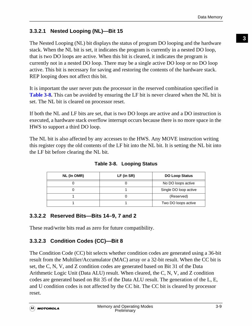
Data Memory
�Memory and Operating Modes 3-9
Preliminary
33.3.2.1 Nested Looping (NL)—Bit 15
The Nested Looping (NL) bit displays the status of program DO looping and the hardware stack. When the NL bit is set, it indicates the program is currently in a nested DO loop, that is two DO loops are active. When this bit is cleared, it indicates the program is currently not in a nested DO loop. There may be a single active DO loop or no DO loop active. This bit is necessary for saving and restoring the contents of the hardware stack. REP looping does not affect this bit.
It is important the user never puts the processor in the reserved combination specified in Table 3-8. This can be avoided by ensuring the LF bit is never cleared when the NL bit is set. The NL bit is cleared on processor reset.
If both the NL and LF bits are set, that is two DO loops are active and a DO instruction is executed, a hardware stack overflow interrupt occurs because there is no more space in the HWS to support a third DO loop.
The NL bit is also affected by any accesses to the HWS. Any MOVE instruction writing this register copy the old contents of the LF bit into the NL bit. It is setting the NL bit into the LF bit before clearing the NL bit.
Table 3-8. Looping Status
3.3.2.2 Reserved Bits—Bits 14–9, 7 and 2
These read/write bits read as zero for future compatibility.
3.3.2.3 Condition Codes (CC)—Bit 8
The Condition Code (CC) bit selects whether condition codes are generated using a 36-bit result from the Multilier/Accumulator (MAC) array or a 32-bit result. When the CC bit is set, the C, N, V, and Z condition codes are generated based on Bit 31 of the Data Arithmetic Logic Unit (Data ALU) result. When cleared, the C, N, V, and Z condition codes are generated based on Bit 35 of the Data ALU result. The generation of the L, E, and U condition codes is not affected by the CC bit. The CC bit is cleared by processor reset.
NL (In OMR) LF (in SR) DO Loop Status
0 0 No DO loops active
0 1 Single DO loop active
1 0 (Reserved)
1 1 Two DO loops active
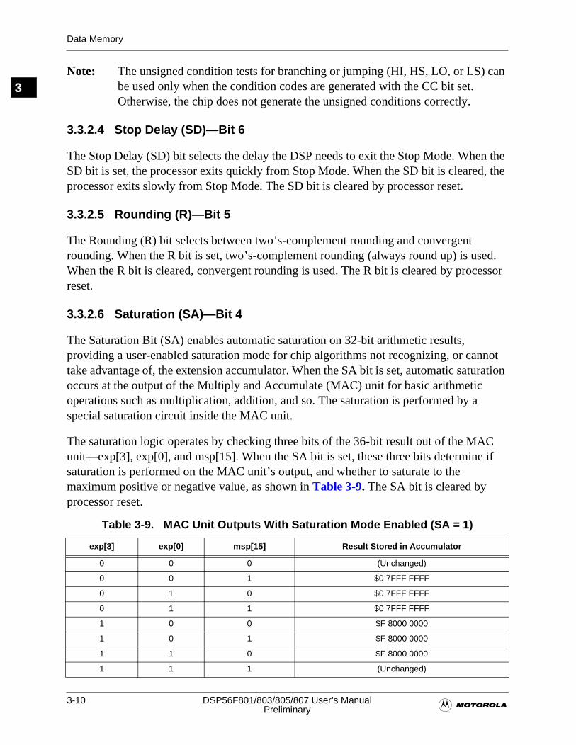
3-10 DSP56F801/803/805/807 User’s Manual�Preliminary
Data Memory
3Note: The unsigned condition tests for branching or jumping (HI, HS, LO, or LS) can
be used only when the condition codes are generated with the CC bit set. Otherwise, the chip does not generate the unsigned conditions correctly.
3.3.2.4 Stop Delay (SD)—Bit 6
The Stop Delay (SD) bit selects the delay the DSP needs to exit the Stop Mode. When the SD bit is set, the processor exits quickly from Stop Mode. When the SD bit is cleared, the processor exits slowly from Stop Mode. The SD bit is cleared by processor reset.
3.3.2.5 Rounding (R)—Bit 5
The Rounding (R) bit selects between two’s-complement rounding and convergent rounding. When the R bit is set, two’s-complement rounding (always round up) is used. When the R bit is cleared, convergent rounding is used. The R bit is cleared by processor reset.
3.3.2.6 Saturation (SA)—Bit 4
The Saturation Bit (SA) enables automatic saturation on 32-bit arithmetic results, providing a user-enabled saturation mode for chip algorithms not recognizing, or cannot take advantage of, the extension accumulator. When the SA bit is set, automatic saturation occurs at the output of the Multiply and Accumulate (MAC) unit for basic arithmetic operations such as multiplication, addition, and so. The saturation is performed by a special saturation circuit inside the MAC unit.
The saturation logic operates by checking three bits of the 36-bit result out of the MAC unit—exp[3], exp[0], and msp[15]. When the SA bit is set, these three bits determine if saturation is performed on the MAC unit’s output, and whether to saturate to the maximum positive or negative value, as shown in Table 3-9. The SA bit is cleared by processor reset.
Table 3-9. MAC Unit Outputs With Saturation Mode Enabled (SA = 1)
exp[3] exp[0] msp[15] Result Stored in Accumulator
0 0 0 (Unchanged)
0 0 1 $0 7FFF FFFF
0 1 0 $0 7FFF FFFF
0 1 1 $0 7FFF FFFF
1 0 0 $F 8000 0000
1 0 1 $F 8000 0000
1 1 0 $F 8000 0000
1 1 1 (Unchanged)
Core Configuration Memory Map
�Memory and Operating Modes 3-11
Preliminary
3Note: Saturation mode is always disabled during the execution of the following
instructions: ASLL, ASRR, LSLL, LSRR, ASRAC, LSRAC, IMPY16, MPYSU, MACSU, AND, OR, EOR, NOT, LSL, LSR, ROL, and ROR. For these instructions, no saturation is performed at the output of the MAC unit.
3.3.2.7 External X Memory (EX)—Bit 3
The External X Memory (EX) bit is necessary for providing a continuous memory map when using more than 64K of external data memory. When the EX bit is set, all accesses to X memory on the X Address Bus 1 (XAB1) and Core Global Data Bus (CGDB) or Peripheral Global Data Bus (PGDB) are forced to be external, except when a MOVE or bit-field instruction is executed using the I/O Short Addressing Mode. In this case, the EX bit is ignored and the access is performed to the on-chip location. When the EX bit is cleared, internal X memory can be accessed with all addressing modes.
The EX bit is ignored by the second read of a dual-read instruction, using the X address Bus 2 (XAB2) and X Data Bus 2 (XDB2) and always accesses on-chip X data memory. For instructions with two parallel reads, the second read is always performed to internal on-chip memory.
Note: When the EX bit is set, only the upper 64-peripheral memory-mapped locations are accessible (x:$FFCO-x:$FF80) with the I/O Short Addressing Mode. The lower 64-memory-mapped locations (X:$FF80–$FFBF) are not accessible when the EX bit is set. Access to these addresses results in an access to external memory.
The EX bit is cleared by processor reset.
3.3.2.8 Operating Mode B (MB)—Bit 1
This bit is latched from the EXTBOOT pin on reset. See Section 3.7 DSP56800 Operating Modes in the DSP56800 Family Manual.
3.3.2.9 Operating Mode A (MA)—Bit 0
This bit is latched from the EXTBOOT pin on reset. See Section 3.7 DSP56800 Operating Modes in the DSP56800 Family Manual.
3.4 Core Configuration Memory Map
Core configuration registers are part of the data memory map on the DSP56800 parts. These locations may be accessed with the same addressing modes used for ordinary data memory when the EX bit is cleared. However, when the EX bit is set, the addresses can only be accessed using the I/O Short Addressing Mode. These registers are implemented
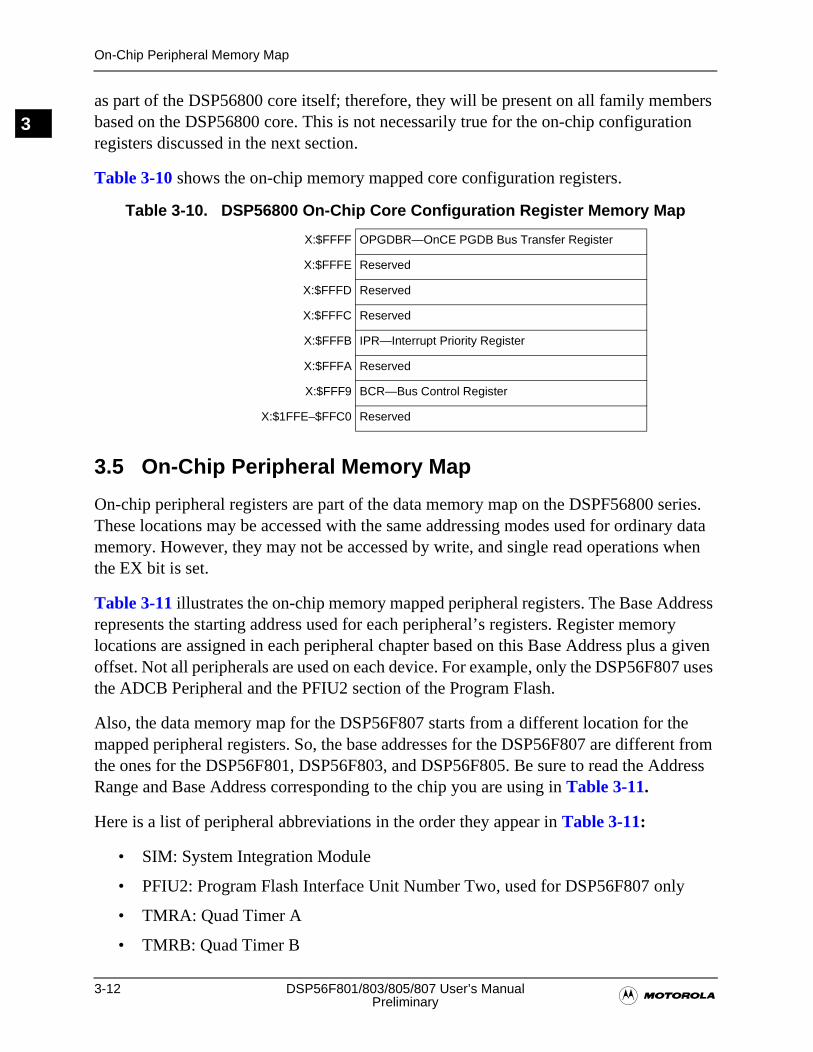
3-12 DSP56F801/803/805/807 User’s Manual�Preliminary
On-Chip Peripheral Memory Map
3as part of the DSP56800 core itself; therefore, they will be present on all family members based on the DSP56800 core. This is not necessarily true for the on-chip configuration registers discussed in the next section.
Table 3-10 shows the on-chip memory mapped core configuration registers.
3.5 On-Chip Peripheral Memory Map
On-chip peripheral registers are part of the data memory map on the DSPF56800 series. These locations may be accessed with the same addressing modes used for ordinary data memory. However, they may not be accessed by write, and single read operations when the EX bit is set.
Table 3-11 illustrates the on-chip memory mapped peripheral registers. The Base Address represents the starting address used for each peripheral’s registers. Register memory locations are assigned in each peripheral chapter based on this Base Address plus a given offset. Not all peripherals are used on each device. For example, only the DSP56F807 uses the ADCB Peripheral and the PFIU2 section of the Program Flash.
Also, the data memory map for the DSP56F807 starts from a different location for the mapped peripheral registers. So, the base addresses for the DSP56F807 are different from the ones for the DSP56F801, DSP56F803, and DSP56F805. Be sure to read the Address Range and Base Address corresponding to the chip you are using in Table 3-11.
Here is a list of peripheral abbreviations in the order they appear in Table 3-11:
• SIM: System Integration Module
• PFIU2: Program Flash Interface Unit Number Two, used for DSP56F807 only
• TMRA: Quad Timer A
• TMRB: Quad Timer B
Table 3-10. DSP56800 On-Chip Core Configuration Register Memory Map
X:$FFFF OPGDBR—OnCE PGDB Bus Transfer Register
X:$FFFE Reserved
X:$FFFD Reserved
X:$FFFC Reserved
X:$FFFB IPR—Interrupt Priority Register
X:$FFFA Reserved
X:$FFF9 BCR—Bus Control Register
X:$1FFE–$FFC0 Reserved

On-Chip Peripheral Memory Map
�Memory and Operating Modes 3-13
Preliminary
3• TMRC: Quad Timer C
• TMRD: Quad Timer D
• CAN: Controller Area Network
• PWMA: Pulse Width Modulator Module A
• PWMB: Pulse Width Modulator Module B
• DEC0: Quadrature Decoder Zero
• DEC1: Quadrature Decoder One
• ITCN: Interrupt Controller
• ADCA: Analog-to-Digital Converter A
• ADCB: Analog-to-Digital Converter B, used for DSP56F807 only
• SCI0: Serial Communications Interface zero
• SCI1: Serial Communications Interface one
• SPI: Serial Peripheral Interface
• COP: Computer Operation Properly
• PFIU: Program Flash Interface Unit
• DFIU: Data Flash Interface Unit
• BFIU: Boot Flash Interface Unit
• CLKGEN: Clock Generation
• GPIOA: General Purpose I/O Port A
• GPIOB: General Purpose I/O Port B
• GPIOD: General Purpose I/O Port D
• GPIOE: General Purpose I/O Port E
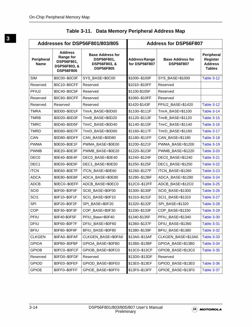
3-14 DSP56F801/803/805/807 User’s Manual�Preliminary
On-Chip Peripheral Memory Map
3Table 3-11. Data Memory Peripheral Address Map
Addresses for DSP56F801/803/805 Address for DSP56F807
Peripheral Name
Address Range for
DSP56F801, DSP56F803, &
DSP56F805
Base Address for DSP56F801,
DSP56F803, & DSP56F805
Address Range for DSP56F807
Base Address for DSP56F807
Peripheral Register Address Tables
SIM $0C00–$0C0F SYS_BASE=$0C00 $1000–$100F SYS_BASE=$1000 Table 3-12
Reserved $0C10–$0CFF Reserved $1010–$10FF Reserved
PFIU2 $0C40–$0C5F Reserved $1100-$105F Reserved
Reserved $0C60–$0CFF Reserved $1060–$10FF Reserved
Reserved Reserved Reserved $1420-$143F PFIU2_BASE=$1420 Table 3-12
TMRA $0D00–$0D1F TmrA_BASE=$0D00 $1100–$111F TmrA_BASE=$1100 Table 3-14
TMRB $0D20–$0D3F TmrB_BASE=$0D20 $1120–$113F TmrB_BASE=$1120 Table 3-15
TMRC $0D40–$0D5F TmrC_BASE=$0D40 $1140–$115F TmrC_BASE=$1140 Table 3-16
TMRD $0D60–$0D7F TmrD_BASE=$0D60 $1160–$117F TmrD_BASE=$1160 Table 3-17
CAN $0D80–$0DFF CAN_BASE=$0D80 $1180–$11FF CAN_BASE=$1180 Table 3-18
PWMA $0E00–$0E1F PWMA_BASE=$0E00 $1200–$121F PWMA_BASE=$1200 Table 3-19
PWMB $0E20–$0E3F PWMB_BASE=$0E20 $1220–$123F PWMB_BASE=$1220 Table 3-20
DEC0 $0E40–$0E4F DEC0_BASE=$0E40 $1240–$124F DEC0_BASE=$1240 Table 3-21
DEC1 $0E50–$0E5F DEC1_BASE=$0E50 $1250–$125F DEC1_BASE=$1250 Table 3-22
ITCN $0E60–$0E7F ITCN_BASE=$0E60 $1260–$127F ITCN_BASE=$1260 Table 3-23
ADCA $0E80–$0EBF ADCA_BASE=$0E80 $1280–$12BF ADCA_BASE=$1280 Table 3-24
ADCB $0EC0–$0EFF ADCB_BASE=$0EC0 $12C0–$12FF ADCB_BASE=$12C0 Table 3-25
SCI0 $0F00–$0F0F SCI0_BASE=$0F00 $1300–$130F SCI0_BASE=$1300 Table 3-26
SCI1 $0F10–$0F1F SCI1_BASE=$0F10 $1310–$131F SCI1_BASE=$1310 Table 3-27
SPI $0F20–$0F2F SPI_BASE=$0F20 $1320–$132F SPI_BASE=$1320 Table 3-28
COP $0F30–$0F3F COP_BASE=$0F30 $1330–$133F COP_BASE=$1330 Table 3-29
PFIU $0F40-$0F5F PFIU_Base=$0F40 $1340-$135F PFIU_BASE=$1340 Table 3-30
DFIU $0F60–$0F7F DFIU_BASE=$0F60 $1360–$137F DFIU_BASE=$1360 Table 3-31
BFIU $0F80–$0F9F BFIU_BASE=$0F80 $1380–$139F BFIU_BASE=$1380 Table 3-32
CLKGEN $0FA0–$0FAF CLKGEN_BASE=$0FA0 $13A0–$13AF CLKGEN_BASE=$13A0 Table 3-33
GPIOA $0FB0–$0FBF GPIOA_BASE=$0FB0 $13B0–$13BF GPIOA_BASE=$13B0 Table 3-34
GPIOB $0FC0–$0FCF GPIOB_BASE=$0FC0 $13C0–$13CF GPIOB_BASE=$13C0 Table 3-35
Reserved $0FD0–$0FDF Reserved $13D0–$13DF Reserved
GPIOD $0FE0–$0FEF GPIOD_BASE=$0FE0 $13E0–$13EF GPIOD_BASE=$13E0 Table 3-36
GPIOE $0FF0–$0FFF GPIOE_BASE=$0FF0 $13F0–$13FF GPIOE_BASE=$13F0 Table 3-37
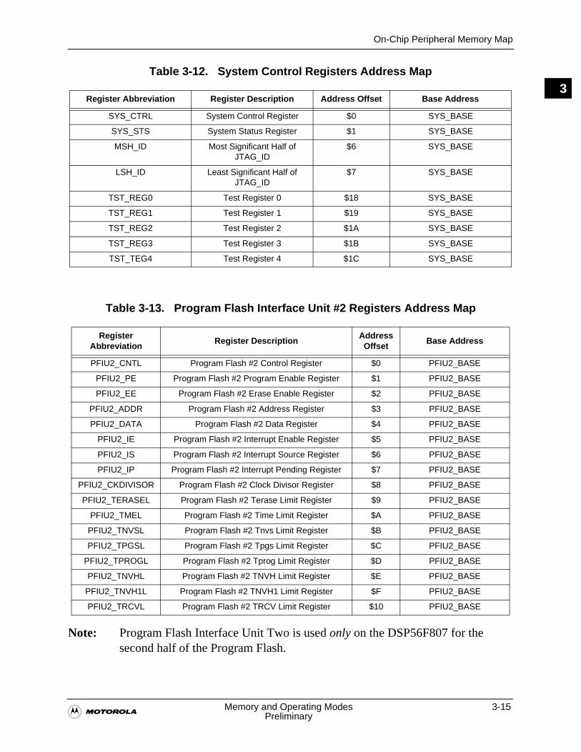
On-Chip Peripheral Memory Map
�Memory and Operating Modes 3-15
Preliminary
3Table 3-12. System Control Registers Address Map
Table 3-13. Program Flash Interface Unit #2 Registers Address Map
Note: Program Flash Interface Unit Two is used only on the DSP56F807 for the second half of the Program Flash.
Register Abbreviation Register Description Address Offset Base Address
SYS_CTRL System Control Register $0 SYS_BASE
SYS_STS System Status Register $1 SYS_BASE
MSH_ID Most Significant Half of JTAG_ID
$6 SYS_BASE
LSH_ID Least Significant Half of JTAG_ID
$7 SYS_BASE
TST_REG0 Test Register 0 $18 SYS_BASE
TST_REG1 Test Register 1 $19 SYS_BASE
TST_REG2 Test Register 2 $1A SYS_BASE
TST_REG3 Test Register 3 $1B SYS_BASE
TST_TEG4 Test Register 4 $1C SYS_BASE
Register Abbreviation
Register DescriptionAddress Offset
Base Address
PFIU2_CNTL Program Flash #2 Control Register $0 PFIU2_BASE
PFIU2_PE Program Flash #2 Program Enable Register $1 PFIU2_BASE
PFIU2_EE Program Flash #2 Erase Enable Register $2 PFIU2_BASE
PFIU2_ADDR Program Flash #2 Address Register $3 PFIU2_BASE
PFIU2_DATA Program Flash #2 Data Register $4 PFIU2_BASE
PFIU2_IE Program Flash #2 Interrupt Enable Register $5 PFIU2_BASE
PFIU2_IS Program Flash #2 Interrupt Source Register $6 PFIU2_BASE
PFIU2_IP Program Flash #2 Interrupt Pending Register $7 PFIU2_BASE
PFIU2_CKDIVISOR Program Flash #2 Clock Divisor Register $8 PFIU2_BASE
PFIU2_TERASEL Program Flash #2 Terase Limit Register $9 PFIU2_BASE
PFIU2_TMEL Program Flash #2 Time Limit Register $A PFIU2_BASE
PFIU2_TNVSL Program Flash #2 Tnvs Limit Register $B PFIU2_BASE
PFIU2_TPGSL Program Flash #2 Tpgs Limit Register $C PFIU2_BASE
PFIU2_TPROGL Program Flash #2 Tprog Limit Register $D PFIU2_BASE
PFIU2_TNVHL Program Flash #2 TNVH Limit Register $E PFIU2_BASE
PFIU2_TNVH1L Program Flash #2 TNVH1 Limit Register $F PFIU2_BASE
PFIU2_TRCVL Program Flash #2 TRCV Limit Register $10 PFIU2_BASE

3-16 DSP56F801/803/805/807 User’s Manual�Preliminary
On-Chip Peripheral Memory Map
3Table 3-14. Quad Timer A Registers Address Map
Register Abbreviation Register Description Address Offset Base Address
TMRA0_CMP1 Compare Register $0 TMRA_BASE
TMRA0_CMP2 Compare Register $1 TMRA_BASE
TMRA0_CAP Capture Register $2 TMRA_BASE
TMRA0_LOAD Load Register $3 TMRA_BASE
TMRA0_HOLD Hold Register $4 TMRA_BASE
TMRA0_CNTR Counter $5 TMRA_BASE
TMRA0_CTRL Control Register $6 TMRA_BASE
TMRA0_SCR Status and Control Register $7 TMRA_BASE
TMRA1_CMP1 Compare Register $8 TMRA_BASE
TMRA1_CMP2 Compare Register $9 TMRA_BASE
TMRA1_CAP Capture Register $A TMRA_BASE
TMRA1_LOAD Load Register $B TMRA_BASE
TMRA1_HOLD Hold Register $C TMRA_BASE
TMRA1_CNTR Counter $D TMRA_BASE
TMRA1_CTRL Control Register $E TMRA_BASE
TMRA1_SCR Status and Control Register $F TMRA_BASE
TMRA2_CMP1 Compare Register $10 TMRA_BASE
TMRA2_CMP2 Compare Register $11 TMRA_BASE
TMRA2_CAP Capture Register $12 TMRA_BASE
TMRA2_LOAD Load Register $13 TMRA_BASE
TMRA2_HOLD Hold Register $14 TMRA_BASE
TMRA2_CNTR Counter $15 TMRA_BASE
TMRA2_CTRL Control Register $16 TMRA_BASE
TMRA2_SCR Status and Control Register $17 TMRA_BASE
TMRA3_CMP1 Compare Register $18 TMRA_BASE
TMRA3_CMP2 Compare Register $19 TMRA_BASE
TMRA3_CAP Capture Register $1A TMRA_BASE
TMRA3_LOAD Load Register $1B TMRA_BASE
TMRA3_HOLD Hold Register $1C TMRA_BASE
TMRA3_CNTR Counter $1D TMRA_BASE
TMRA3_CTRL Control Register $1E TMRA_BASE
TMRA3_SCR Status and Control Register $1F TMRA_BASE
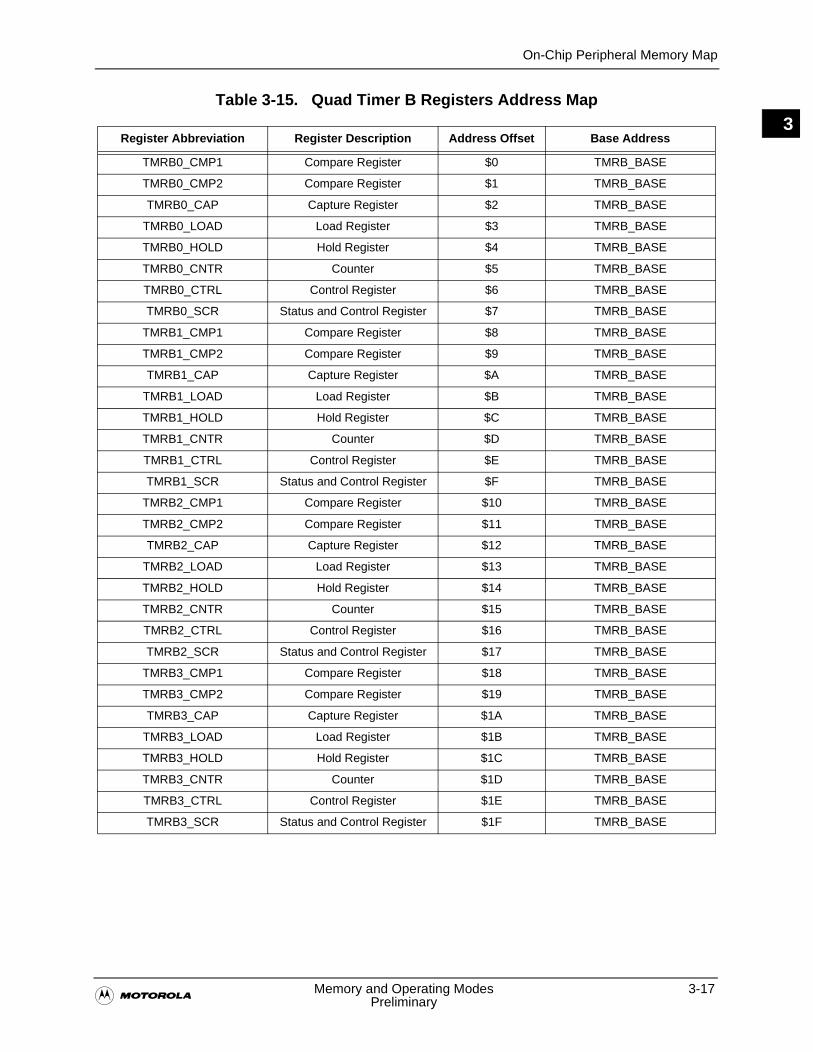
On-Chip Peripheral Memory Map
�Memory and Operating Modes 3-17
Preliminary
3Table 3-15. Quad Timer B Registers Address Map
Register Abbreviation Register Description Address Offset Base Address
TMRB0_CMP1 Compare Register $0 TMRB_BASE
TMRB0_CMP2 Compare Register $1 TMRB_BASE
TMRB0_CAP Capture Register $2 TMRB_BASE
TMRB0_LOAD Load Register $3 TMRB_BASE
TMRB0_HOLD Hold Register $4 TMRB_BASE
TMRB0_CNTR Counter $5 TMRB_BASE
TMRB0_CTRL Control Register $6 TMRB_BASE
TMRB0_SCR Status and Control Register $7 TMRB_BASE
TMRB1_CMP1 Compare Register $8 TMRB_BASE
TMRB1_CMP2 Compare Register $9 TMRB_BASE
TMRB1_CAP Capture Register $A TMRB_BASE
TMRB1_LOAD Load Register $B TMRB_BASE
TMRB1_HOLD Hold Register $C TMRB_BASE
TMRB1_CNTR Counter $D TMRB_BASE
TMRB1_CTRL Control Register $E TMRB_BASE
TMRB1_SCR Status and Control Register $F TMRB_BASE
TMRB2_CMP1 Compare Register $10 TMRB_BASE
TMRB2_CMP2 Compare Register $11 TMRB_BASE
TMRB2_CAP Capture Register $12 TMRB_BASE
TMRB2_LOAD Load Register $13 TMRB_BASE
TMRB2_HOLD Hold Register $14 TMRB_BASE
TMRB2_CNTR Counter $15 TMRB_BASE
TMRB2_CTRL Control Register $16 TMRB_BASE
TMRB2_SCR Status and Control Register $17 TMRB_BASE
TMRB3_CMP1 Compare Register $18 TMRB_BASE
TMRB3_CMP2 Compare Register $19 TMRB_BASE
TMRB3_CAP Capture Register $1A TMRB_BASE
TMRB3_LOAD Load Register $1B TMRB_BASE
TMRB3_HOLD Hold Register $1C TMRB_BASE
TMRB3_CNTR Counter $1D TMRB_BASE
TMRB3_CTRL Control Register $1E TMRB_BASE
TMRB3_SCR Status and Control Register $1F TMRB_BASE
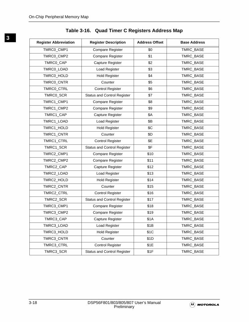
3-18 DSP56F801/803/805/807 User’s Manual�Preliminary
On-Chip Peripheral Memory Map
3Table 3-16. Quad Timer C Registers Address Map
Register Abbreviation Register Description Address Offset Base Address
TMRC0_CMP1 Compare Register $0 TMRC_BASE
TMRC0_CMP2 Compare Register $1 TMRC_BASE
TMRC0_CAP Capture Register $2 TMRC_BASE
TMRC0_LOAD Load Register $3 TMRC_BASE
TMRC0_HOLD Hold Register $4 TMRC_BASE
TMRC0_CNTR Counter $5 TMRC_BASE
TMRC0_CTRL Control Register $6 TMRC_BASE
TMRC0_SCR Status and Control Register $7 TMRC_BASE
TMRC1_CMP1 Compare Register $8 TMRC_BASE
TMRC1_CMP2 Compare Register $9 TMRC_BASE
TMRC1_CAP Capture Register $A TMRC_BASE
TMRC1_LOAD Load Register $B TMRC_BASE
TMRC1_HOLD Hold Register $C TMRC_BASE
TMRC1_CNTR Counter $D TMRC_BASE
TMRC1_CTRL Control Register $E TMRC_BASE
TMRC1_SCR Status and Control Register $F TMRC_BASE
TMRC2_CMP1 Compare Register $10 TMRC_BASE
TMRC2_CMP2 Compare Register $11 TMRC_BASE
TMRC2_CAP Capture Register $12 TMRC_BASE
TMRC2_LOAD Load Register $13 TMRC_BASE
TMRC2_HOLD Hold Register $14 TMRC_BASE
TMRC2_CNTR Counter $15 TMRC_BASE
TMRC2_CTRL Control Register $16 TMRC_BASE
TMRC2_SCR Status and Control Register $17 TMRC_BASE
TMRC3_CMP1 Compare Register $18 TMRC_BASE
TMRC3_CMP2 Compare Register $19 TMRC_BASE
TMRC3_CAP Capture Register $1A TMRC_BASE
TMRC3_LOAD Load Register $1B TMRC_BASE
TMRC3_HOLD Hold Register $1C TMRC_BASE
TMRC3_CNTR Counter $1D TMRC_BASE
TMRC3_CTRL Control Register $1E TMRC_BASE
TMRC3_SCR Status and Control Register $1F TMRC_BASE

On-Chip Peripheral Memory Map
�Memory and Operating Modes 3-19
Preliminary
3Table 3-17. Quad Timer D Registers Address Map
Register Abbreviation Register Description Address Offset Base Address
TMRD0_CMP1 Compare Register $0 TMRD_BASE
TMRD0_CMP2 Compare Register $1 TMRD_BASE
TMRD0_CAP Capture Register $2 TMRD_BASE
TMRD0_LOAD Load Register $3 TMRD_BASE
TMRD0_HOLD Hold Register $4 TMRD_BASE
TMRD0_CNTR Counter $5 TMRD_BASE
TMRD0_CTRL Control Register $6 TMRD_BASE
TMRD0_SCR Status and Control Register $7 TMRD_BASE
TMRD1_CMP1 Compare Register $8 TMRD_BASE
TMRD1_CMP2 Compare Register $9 TMRD_BASE
TMRD1_CAP Capture Register $A TMRD_BASE
TMRD1_LOAD Load Register $B TMRD_BASE
TMRD1_HOLD Hold Register $C TMRD_BASE
TMRD1_CNTR Counter $D TMRD_BASE
TMRD1_CTRL Control Register $E TMRD_BASE
TMRD1_SCR Status and Control Register $F TMRD_BASE
TMRD2_CMP1 Compare Register $10 TMRD_BASE
TMRD2_CMP2 Compare Register $11 TMRD_BASE
TMRD2_CAP Capture Register $12 TMRD_BASE
TMRD2_LOAD Load Register $13 TMRD_BASE
TMRD2_HOLD Hold Register $14 TMRD_BASE
TMRD2_CNTR Counter $15 TMRD_BASE
TMRD2_CTRL Control Register $16 TMRD_BASE
TMRD2_SCR Status and Control Register $17 TMRD_BASE
TMRD3_CMP1 Compare Register $18 TMRD_BASE
TMRD3_CMP2 Compare Register $19 TMRD_BASE
TMRD3_CAP Capture Register $1A TMRD_BASE
TMRD3_LOAD Load Register $1B TMRD_BASE
TMRD3_HOLD Hold Register $1C TMRD_BASE
TMRD3_CNTR Counter $1D TMRD_BASE
TMRD3_CTRL Control Register $1E TMRD_BASE
TMRD3_SCR Status and Control Register $1F TMRD_BASE
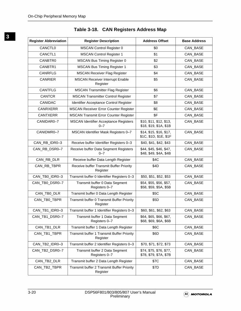
3-20 DSP56F801/803/805/807 User’s Manual�Preliminary
On-Chip Peripheral Memory Map
3Table 3-18. CAN Registers Address Map
Register Abbreviation Register Description Address Offset Base Address
CANCTL0 MSCAN Control Register 0 $0 CAN_BASE
CANCTL1 MSCAN Control Register 1 $1 CAN_BASE
CANBTR0 MSCAN Bus Timing Register 0 $2 CAN_BASE
CANBTR1 MSCAN Bus Timing Register 1 $3 CAN_BASE
CANRFLG MSCAN Receiver Flag Register $4 CAN_BASE
CANRIER MSCAN Receiver Interrupt Enable Register
$5 CAN_BASE
CANTFLG MSCAN Transmitter Flag Register $6 CAN_BASE
CANTCR MSCAN Transmitter Control Register $7 CAN_BASE
CANIDAC Identifier Acceptance Control Register $8 CAN_BASE
CANRXERR MSCAN Receiver Error Counter Register $E CAN_BASE
CANTXERR MSCAN Transmit Error Counter Register $F CAN_BASE
CANIDAR0–7 MSCAN Identifier Acceptance Registers 0–7
$10, $11, $12, $13, $18, $19, $1A, $1B
CAN_BASE
CANIDMR0–7 MSCAN Identifier Mask Registers 0–7 $14, $15, $16, $17, $1C, $1D, $1E, $1F
CAN_BASE
CAN_RB_IDR0–3 Receive buffer Identifier Registers 0–3 $40, $41, $42, $43 CAN_BASE
CAN_RB_DSR0–7 Receive buffer Data Segment Registers 0–7
$44, $45, $46, $47, $48, $49, $4A, $4B
CAN_BASE
CAN_RB_DLR Receive buffer Data Length Register $4C CAN_BASE
CAN_RB_TBPR Receive buffer Transmit Buffer Priority Register
$4D CAN_BASE
CAN_TB0_IDR0–3 Transmit buffer 0 Identifier Registers 0–3 $50, $51, $52, $53 CAN_BASE
CAN_TB0_DSR0–7 Transmit buffer 0 Data Segment Registers 0–7
$54, $55, $56, $57, $58, $59, $5A, $5B
CAN_BASE
CAN_TB0_DLR Transmit buffer 0 Data Length Register $5C CAN_BASE
CAN_TB0_TBPR Transmit buffer 0 Transmit Buffer Priority Register
$5D CAN_BASE
CAN_TB1_IDR0–3 Transmit buffer 1 Identifier Registers 0–3 $60, $61, $62, $63 CAN_BASE
CAN_TB1_DSR0–7 Transmit buffer 1 Data Segment Registers 0–7
$64, $65, $66, $67, $68, $69, $6A, $6B
CAN_BASE
CAN_TB1_DLR Transmit buffer 1 Data Length Register $6C CAN_BASE
CAN_TB1_TBPR Transmit buffer 1 Transmit Buffer Priority Register
$6D CAN_BASE
CAN_TB2_IDR0–3 Transmit buffer 2 Identifier Registers 0–3 $70, $71, $72, $73 CAN_BASE
CAN_TB2_DSR0–7 Transmit buffer 2 Data Segment Registers 0–7
$74, $75, $76, $77, $78, $79, $7A, $7B
CAN_BASE
CAN_TB2_DLR Transmit buffer 2 Data Length Register $7C CAN_BASE
CAN_TB2_TBPR Transmit buffer 2 Transmit Buffer Priority Register
$7D CAN_BASE
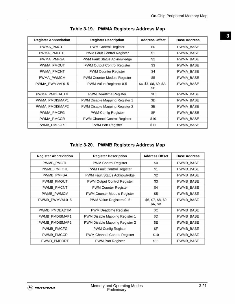
On-Chip Peripheral Memory Map
�Memory and Operating Modes 3-21
Preliminary
3Table 3-19. PWMA Registers Address Map
Table 3-20. PWMB Registers Address Map
Register Abbreviation Register Description Address Offset Base Address
PWMA_PMCTL PWM Control Register $0 PWMA_BASE
PWMA_PMFCTL PWM Fault Control Register $1 PWMA_BASE
PWMA_PMFSA PWM Fault Status Acknowledge $2 PWMA_BASE
PWMA_PMOUT PWM Output Control Register $3 PWMA_BASE
PWMA_PMCNT PWM Counter Register $4 PWMA_BASE
PWMA_PWMCM PWM Counter Modulo Register $5 PWMA_BASE
PWMA_PWMVAL0–5 PWM Value Registers 0-5 $6, $7, $8, $9, $A, $B
PWMA_BASE
PWMA_PMDEADTM PWM Deadtime Register $C PWMA_BASE
PWMA_PMDISMAP1 PWM Disable Mapping Register 1 $D PWMA_BASE
PWMA_PMDISMAP2 PWM Disable Mapping Register 2 $E PWMA_BASE
PWMA_PMCFG PWM Config Register $F PWMA_BASE
PWMA_PMCCR PWM Channel Control Register $10 PWMA_BASE
PWMA_PMPORT PWM Port Register $11 PWMA_BASE
Register Abbreviation Register Description Address Offset Base Address
PWMB_PMCTL PWM Control Register $0 PWMB_BASE
PWMB_PMFCTL PWM Fault Control Register $1 PWMB_BASE
PWMB_PMFSA PWM Fault Status Acknowledge $2 PWMB_BASE
PWMB_PMOUT PWM Output Control Register $3 PWMB_BASE
PWMB_PMCNT PWM Counter Register $4 PWMB_BASE
PWMB_PWMCM PWM Counter Modulo Register $5 PWMB_BASE
PWMB_PWMVAL0–5 PWM Value Registers 0–5 $6, $7, $8, $9$A, $B
PWMB_BASE
PWMB_PMDEADTM PWM Deadtime Register $C PWMB_BASE
PWMB_PMDISMAP1 PWM Disable Mapping Register 1 $D PWMB_BASE
PWMB_PMDISMAP2 PWM Disable Mapping Register 2 $E PWMB_BASE
PWMB_PMCFG PWM Config Register $F PWMB_BASE
PWMB_PMCCR PWM Channel Control Register $10 PWMB_BASE
PWMB_PMPORT PWM Port Register $11 PWMB_BASE
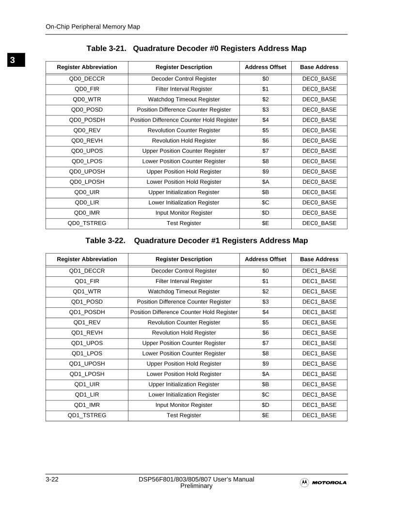
3-22 DSP56F801/803/805/807 User’s Manual�Preliminary
On-Chip Peripheral Memory Map
3Table 3-21. Quadrature Decoder #0 Registers Address Map
Table 3-22. Quadrature Decoder #1 Registers Address Map
Register Abbreviation Register Description Address Offset Base Address
QD0_DECCR Decoder Control Register $0 DEC0_BASE
QD0_FIR Filter Interval Register $1 DEC0_BASE
QD0_WTR Watchdog Timeout Register $2 DEC0_BASE
QD0_POSD Position Difference Counter Register $3 DEC0_BASE
QD0_POSDH Position Difference Counter Hold Register $4 DEC0_BASE
QD0_REV Revolution Counter Register $5 DEC0_BASE
QD0_REVH Revolution Hold Register $6 DEC0_BASE
QD0_UPOS Upper Position Counter Register $7 DEC0_BASE
QD0_LPOS Lower Position Counter Register $8 DEC0_BASE
QD0_UPOSH Upper Position Hold Register $9 DEC0_BASE
QD0_LPOSH Lower Position Hold Register $A DEC0_BASE
QD0_UIR Upper Initialization Register $B DEC0_BASE
QD0_LIR Lower Initialization Register $C DEC0_BASE
QD0_IMR Input Monitor Register $D DEC0_BASE
QD0_TSTREG Test Register $E DEC0_BASE
Register Abbreviation Register Description Address Offset Base Address
QD1_DECCR Decoder Control Register $0 DEC1_BASE
QD1_FIR Filter Interval Register $1 DEC1_BASE
QD1_WTR Watchdog Timeout Register $2 DEC1_BASE
QD1_POSD Position Difference Counter Register $3 DEC1_BASE
QD1_POSDH Position Difference Counter Hold Register $4 DEC1_BASE
QD1_REV Revolution Counter Register $5 DEC1_BASE
QD1_REVH Revolution Hold Register $6 DEC1_BASE
QD1_UPOS Upper Position Counter Register $7 DEC1_BASE
QD1_LPOS Lower Position Counter Register $8 DEC1_BASE
QD1_UPOSH Upper Position Hold Register $9 DEC1_BASE
QD1_LPOSH Lower Position Hold Register $A DEC1_BASE
QD1_UIR Upper Initialization Register $B DEC1_BASE
QD1_LIR Lower Initialization Register $C DEC1_BASE
QD1_IMR Input Monitor Register $D DEC1_BASE
QD1_TSTREG Test Register $E DEC1_BASE
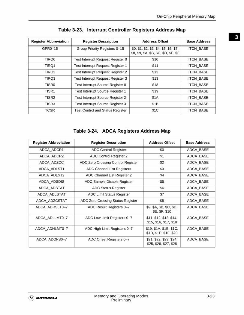
On-Chip Peripheral Memory Map
�Memory and Operating Modes 3-23
Preliminary
3Table 3-23. Interrupt Controller Registers Address Map
Table 3-24. ADCA Registers Address Map
Register Abbreviation Register Description Address Offset Base Address
GPR0–15 Group Priority Registers 0–15 $0, $1, $2, $3, $4, $5, $6, $7, $8, $9, $A, $B, $C, $D, $E, $F
ITCN_BASE
TIRQ0 Test Interrupt Request Register 0 $10 ITCN_BASE
TIRQ1 Test Interrupt Request Register 1 $11 ITCN_BASE
TIRQ2 Test Interrupt Request Register 2 $12 ITCN_BASE
TIRQ3 Test Interrupt Request Register 3 $13 ITCN_BASE
TISR0 Test Interrupt Source Register 0 $18 ITCN_BASE
TISR1 Test Interrupt Source Register 1 $19 ITCN_BASE
TISR2 Test Interrupt Source Register 2 $1A ITCN_BASE
TISR3 Test Interrupt Source Register 3 $1B ITCN_BASE
TCSR Test Control and Status Register $1C ITCN_BASE
Register Abbreviation Register Description Address Offset Base Address
ADCA_ADCR1 ADC Control Register $0 ADCA_BASE
ADCA_ADCR2 ADC Control Register 2 $1 ADCA_BASE
ADCA_ADZCC ADC Zero Crossing Control Register $2 ADCA_BASE
ADCA_ADLST1 ADC Channel List Registers $3 ADCA_BASE
ADCA_ADLST2 ADC Channel List Register 2 $4 ADCA_BASE
ADCA_ADSDIS ADC Sample Disable Register $5 ADCA_BASE
ADCA_ADSTAT ADC Status Register $6 ADCA_BASE
ADCA_ADLSTAT ADC Limit Status Register $7 ADCA_BASE
ADCA_ADZCSTAT ADC Zero Crossing Status Register $8 ADCA_BASE
ADCA_ADRSLT0–7 ADC Result Registers 0–7 $9, $A, $B, $C, $D, $E, $F, $10
ADCA_BASE
ADCA_ADLLMT0–7 ADC Low Limit Registers 0–7 $11, $12, $13, $14, $15, $16, $17, $18
ADCA_BASE
ADCA_ADHLMT0–7 ADC High Limit Registers 0–7 $19, $1A, $1B, $1C, $1D, $1E, $1F, $20
ADCA_BASE
ADCA_ADOFS0–7 ADC Offset Registers 0–7 $21, $22, $23, $24, $25, $26, $27, $28
ADCA_BASE
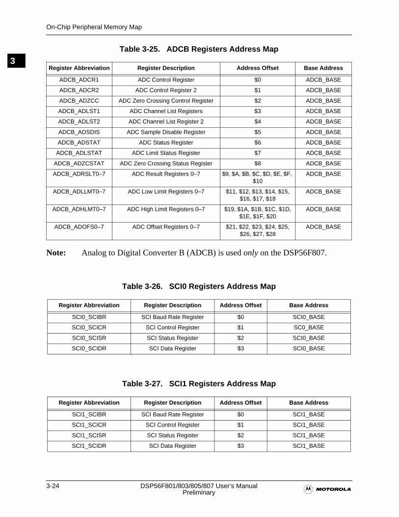
3-24 DSP56F801/803/805/807 User’s Manual�Preliminary
On-Chip Peripheral Memory Map
3Table 3-25. ADCB Registers Address Map
Note: Analog to Digital Converter B (ADCB) is used only on the DSP56F807.
Table 3-26. SCI0 Registers Address Map
Table 3-27. SCI1 Registers Address Map
Register Abbreviation Register Description Address Offset Base Address
ADCB_ADCR1 ADC Control Register $0 ADCB_BASE
ADCB_ADCR2 ADC Control Register 2 $1 ADCB_BASE
ADCB_ADZCC ADC Zero Crossing Control Register $2 ADCB_BASE
ADCB_ADLST1 ADC Channel List Registers $3 ADCB_BASE
ADCB_ADLST2 ADC Channel List Register 2 $4 ADCB_BASE
ADCB_ADSDIS ADC Sample Disable Register $5 ADCB_BASE
ADCB_ADSTAT ADC Status Register $6 ADCB_BASE
ADCB_ADLSTAT ADC Limit Status Register $7 ADCB_BASE
ADCB_ADZCSTAT ADC Zero Crossing Status Register $8 ADCB_BASE
ADCB_ADRSLT0–7 ADC Result Registers 0–7 $9, $A, $B, $C, $D, $E, $F, $10
ADCB_BASE
ADCB_ADLLMT0–7 ADC Low Limit Registers 0–7 $11, $12, $13, $14, $15, $16, $17, $18
ADCB_BASE
ADCB_ADHLMT0–7 ADC High Limit Registers 0–7 $19, $1A, $1B, $1C, $1D, $1E, $1F, $20
ADCB_BASE
ADCB_ADOFS0–7 ADC Offset Registers 0–7 $21, $22, $23, $24, $25, $26, $27, $28
ADCB_BASE
Register Abbreviation Register Description Address Offset Base Address
SCI0_SCIBR SCI Baud Rate Register $0 SCI0_BASE
SCI0_SCICR SCI Control Register $1 SC0_BASE
SCI0_SCISR SCI Status Register $2 SCI0_BASE
SCI0_SCIDR SCI Data Register $3 SCI0_BASE
Register Abbreviation Register Description Address Offset Base Address
SCI1_SCIBR SCI Baud Rate Register $0 SCI1_BASE
SCI1_SCICR SCI Control Register $1 SCI1_BASE
SCI1_SCISR SCI Status Register $2 SCI1_BASE
SCI1_SCIDR SCI Data Register $3 SCI1_BASE
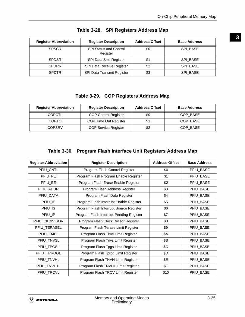
On-Chip Peripheral Memory Map
�Memory and Operating Modes 3-25
Preliminary
3Table 3-28. SPI Registers Address Map
Table 3-29. COP Registers Address Map
Table 3-30. Program Flash Interface Unit Registers Address Map
Register Abbreviation Register Description Address Offset Base Address
SPSCR SPI Status and Control Register
$0 SPI_BASE
SPDSR SPI Data Size Register $1 SPI_BASE
SPDRR SPI Data Receive Register $2 SPI_BASE
SPDTR SPI Data Transmit Register $3 SPI_BASE
Register Abbreviation Register Description Address Offset Base Address
COPCTL COP Control Register $0 COP_BASE
COPTO COP Time Out Register $1 COP_BASE
COPSRV COP Service Register $2 COP_BASE
Register Abbreviation Register Description Address Offset Base Address
PFIU_CNTL Program Flash Control Register $0 PFIU_BASE
PFIU_PE Program Flash Program Enable Register $1 PFIU_BASE
PFIU_EE Program Flash Erase Enable Register $2 PFIU_BASE
PFIU_ADDR Program Flash Address Register $3 PFIU_BASE
PFIU_DATA Program Flash Data Register $4 PFIU_BASE
PFIU_IE Program Flash Interrupt Enable Register $5 PFIU_BASE
PFIU_IS Program Flash Interrupt Source Register $6 PFIU_BASE
PFIU_IP Program Flash Interrupt Pending Register $7 PFIU_BASE
PFIU_CKDIVISOR Program Flash Clock Divisor Register $8 PFIU_BASE
PFIU_TERASEL Program Flash Terase Limit Register $9 PFIU_BASE
PFIU_TMEL Program Flash Time Limit Register $A PFIU_BASE
PFIU_TNVSL Program Flash Tnvs Limit Register $B PFIU_BASE
PFIU_TPGSL Program Flash Tpgs Limit Register $C PFIU_BASE
PFIU_TPROGL Program Flash Tprog Limit Register $D PFIU_BASE
PFIU_TNVHL Program Flash TNVH Limit Register $E PFIU_BASE
PFIU_TNVH1L Program Flash TNVH1 Limit Register $F PFIU_BASE
PFIU_TRCVL Program Flash TRCV Limit Register $10 PFIU_BASE
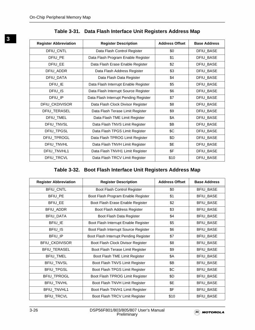
3-26 DSP56F801/803/805/807 User’s Manual�Preliminary
On-Chip Peripheral Memory Map
3Table 3-31. Data Flash Interface Unit Registers Address Map
Table 3-32. Boot Flash Interface Unit Registers Address Map
Register Abbreviation Register Description Address Offset Base Address
DFIU_CNTL Data Flash Control Register $0 DFIU_BASE
DFIU_PE Data Flash Program Enable Register $1 DFIU_BASE
DFIU_EE Data Flash Erase Enable Register $2 DFIU_BASE
DFIU_ADDR Data Flash Address Register $3 DFIU_BASE
DFIU_DATA Data Flash Data Register $4 DFIU_BASE
DFIU_IE Data Flash Interrupt Enable Register $5 DFIU_BASE
DFIU_IS Data Flash Interrupt Source Register $6 DFIU_BASE
DFIU_IP Data Flash Interrupt Pending Register $7 DFIU_BASE
DFIU_CKDIVISOR Data Flash Clock Divisor Register $8 DFIU_BASE
DFIU_TERASEL Data Flash Terase Limit Register $9 DFIU_BASE
DFIU_TMEL Data Flash TME Limit Register $A DFIU_BASE
DFIU_TNVSL Data Flash TNVS Limit Register $B DFIU_BASE
DFIU_TPGSL Data Flash TPGS Limit Register $C DFIU_BASE
DFIU_TPROGL Data Flash TPROG Limit Register $D DFIU_BASE
DFIU_TNVHL Data Flash TNVH Limit Register $E DFIU_BASE
DFIU_TNVHL1 Data Flash TNVH1 Limit Register $F DFIU_BASE
DFIU_TRCVL Data Flash TRCV Limit Register $10 DFIU_BASE
Register Abbreviation Register Description Address Offset Base Address
BFIU_CNTL Boot Flash Control Register $0 BFIU_BASE
BFIU_PE Boot Flash Program Enable Register $1 BFIU_BASE
BFIU_EE Boot Flash Erase Enable Register $2 BFIU_BASE
BFIU_ADDR Boot Flash Address Register $3 BFIU_BASE
BFIU_DATA Boot Flash Data Register $4 BFIU_BASE
BFIU_IE Boot Flash Interrupt Enable Register $5 BFIU_BASE
BFIU_IS Boot Flash Interrupt Source Register $6 BFIU_BASE
BFIU_IP Boot Flash Interrupt Pending Register $7 BFIU_BASE
BFIU_CKDIVISOR Boot Flash Clock Divisor Register $8 BFIU_BASE
BFIU_TERASEL Boot Flash Terase Limit Register $9 BFIU_BASE
BFIU_TMEL Boot Flash TME Limit Register $A BFIU_BASE
BFIU_TNVSL Boot Flash TNVS Limit Register $B BFIU_BASE
BFIU_TPGSL Boot Flash TPGS Limit Register $C BFIU_BASE
BFIU_TPROGL Boot Flash TPROG Limit Register $D BFIU_BASE
BFIU_TNVHL Boot Flash TNVH Limit Register $E BFIU_BASE
BFIU_TNVHL1 Boot Flash TNVH1 Limit Register $F BFIU_BASE
BFIU_TRCVL Boot Flash TRCV Limit Register $10 BFIU_BASE
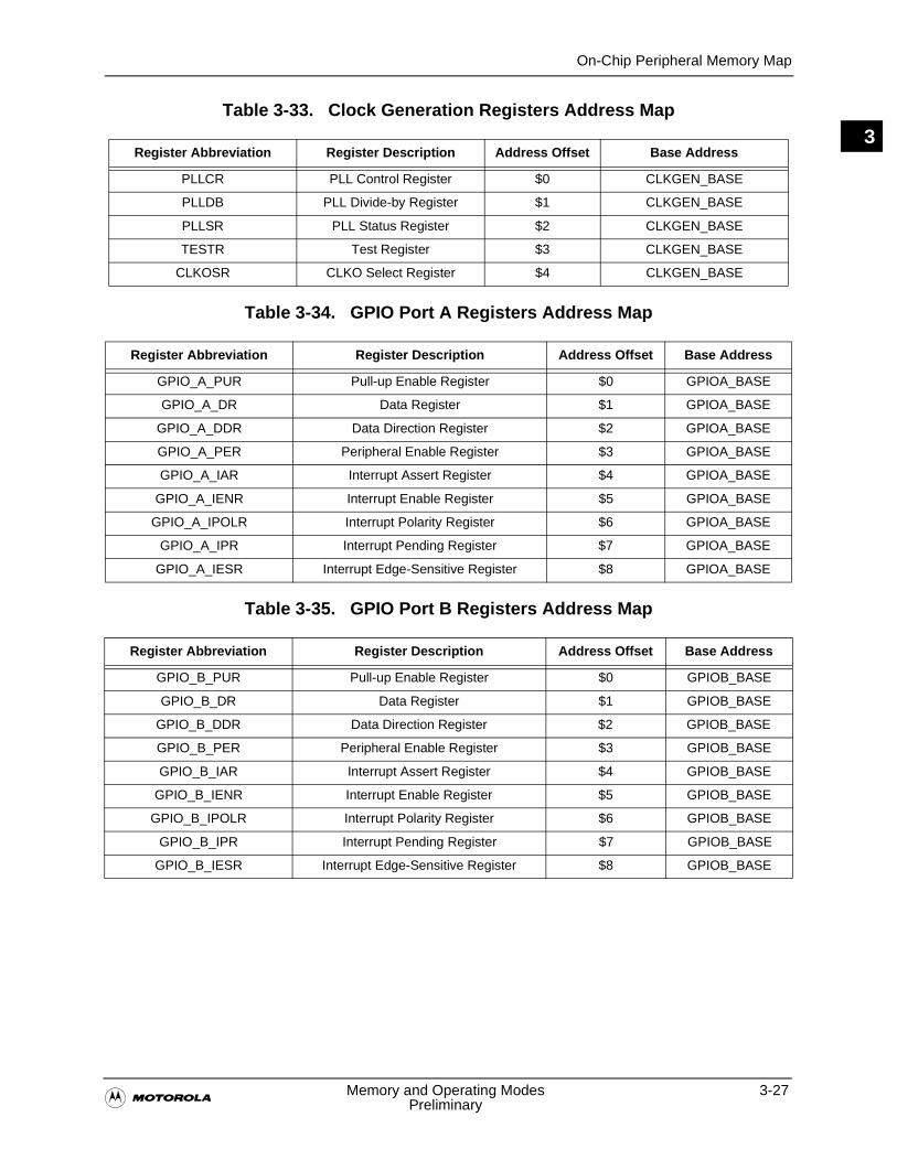
On-Chip Peripheral Memory Map
�Memory and Operating Modes 3-27
Preliminary
3Table 3-33. Clock Generation Registers Address Map
Table 3-34. GPIO Port A Registers Address Map
Table 3-35. GPIO Port B Registers Address Map
Register Abbreviation Register Description Address Offset Base Address
PLLCR PLL Control Register $0 CLKGEN_BASE
PLLDB PLL Divide-by Register $1 CLKGEN_BASE
PLLSR PLL Status Register $2 CLKGEN_BASE
TESTR Test Register $3 CLKGEN_BASE
CLKOSR CLKO Select Register $4 CLKGEN_BASE
Register Abbreviation Register Description Address Offset Base Address
GPIO_A_PUR Pull-up Enable Register $0 GPIOA_BASE
GPIO_A_DR Data Register $1 GPIOA_BASE
GPIO_A_DDR Data Direction Register $2 GPIOA_BASE
GPIO_A_PER Peripheral Enable Register $3 GPIOA_BASE
GPIO_A_IAR Interrupt Assert Register $4 GPIOA_BASE
GPIO_A_IENR Interrupt Enable Register $5 GPIOA_BASE
GPIO_A_IPOLR Interrupt Polarity Register $6 GPIOA_BASE
GPIO_A_IPR Interrupt Pending Register $7 GPIOA_BASE
GPIO_A_IESR Interrupt Edge-Sensitive Register $8 GPIOA_BASE
Register Abbreviation Register Description Address Offset Base Address
GPIO_B_PUR Pull-up Enable Register $0 GPIOB_BASE
GPIO_B_DR Data Register $1 GPIOB_BASE
GPIO_B_DDR Data Direction Register $2 GPIOB_BASE
GPIO_B_PER Peripheral Enable Register $3 GPIOB_BASE
GPIO_B_IAR Interrupt Assert Register $4 GPIOB_BASE
GPIO_B_IENR Interrupt Enable Register $5 GPIOB_BASE
GPIO_B_IPOLR Interrupt Polarity Register $6 GPIOB_BASE
GPIO_B_IPR Interrupt Pending Register $7 GPIOB_BASE
GPIO_B_IESR Interrupt Edge-Sensitive Register $8 GPIOB_BASE
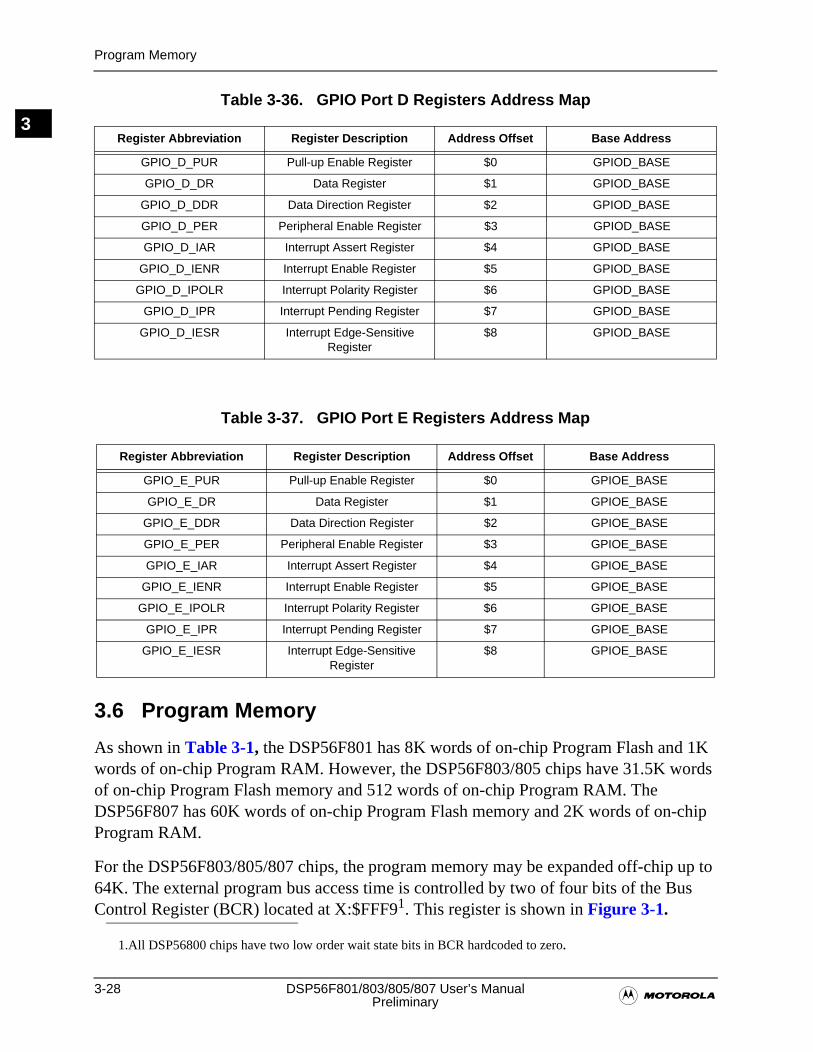
3-28 DSP56F801/803/805/807 User’s Manual�Preliminary
Program Memory
3Table 3-36. GPIO Port D Registers Address Map
Table 3-37. GPIO Port E Registers Address Map
3.6 Program Memory
As shown in Table 3-1, the DSP56F801 has 8K words of on-chip Program Flash and 1K words of on-chip Program RAM. However, the DSP56F803/805 chips have 31.5K words of on-chip Program Flash memory and 512 words of on-chip Program RAM. The DSP56F807 has 60K words of on-chip Program Flash memory and 2K words of on-chip Program RAM.
For the DSP56F803/805/807 chips, the program memory may be expanded off-chip up to 64K. The external program bus access time is controlled by two of four bits of the Bus Control Register (BCR) located at X:$FFF91. This register is shown in Figure 3-1.
Register Abbreviation Register Description Address Offset Base Address
GPIO_D_PUR Pull-up Enable Register $0 GPIOD_BASE
GPIO_D_DR Data Register $1 GPIOD_BASE
GPIO_D_DDR Data Direction Register $2 GPIOD_BASE
GPIO_D_PER Peripheral Enable Register $3 GPIOD_BASE
GPIO_D_IAR Interrupt Assert Register $4 GPIOD_BASE
GPIO_D_IENR Interrupt Enable Register $5 GPIOD_BASE
GPIO_D_IPOLR Interrupt Polarity Register $6 GPIOD_BASE
GPIO_D_IPR Interrupt Pending Register $7 GPIOD_BASE
GPIO_D_IESR Interrupt Edge-Sensitive Register
$8 GPIOD_BASE
Register Abbreviation Register Description Address Offset Base Address
GPIO_E_PUR Pull-up Enable Register $0 GPIOE_BASE
GPIO_E_DR Data Register $1 GPIOE_BASE
GPIO_E_DDR Data Direction Register $2 GPIOE_BASE
GPIO_E_PER Peripheral Enable Register $3 GPIOE_BASE
GPIO_E_IAR Interrupt Assert Register $4 GPIOE_BASE
GPIO_E_IENR Interrupt Enable Register $5 GPIOE_BASE
GPIO_E_IPOLR Interrupt Polarity Register $6 GPIOE_BASE
GPIO_E_IPR Interrupt Pending Register $7 GPIOE_BASE
GPIO_E_IESR Interrupt Edge-Sensitive Register
$8 GPIOE_BASE
1.All DSP56800 chips have two low order wait state bits in BCR hardcoded to zero.
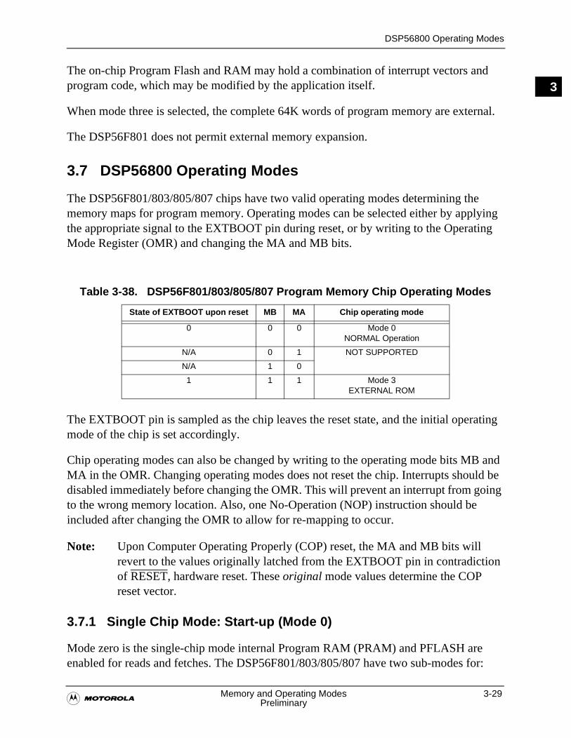
DSP56800 Operating Modes
�Memory and Operating Modes 3-29
Preliminary
3The on-chip Program Flash and RAM may hold a combination of interrupt vectors and program code, which may be modified by the application itself.
When mode three is selected, the complete 64K words of program memory are external.
The DSP56F801 does not permit external memory expansion.
3.7 DSP56800 Operating Modes
The DSP56F801/803/805/807 chips have two valid operating modes determining the memory maps for program memory. Operating modes can be selected either by applying the appropriate signal to the EXTBOOT pin during reset, or by writing to the Operating Mode Register (OMR) and changing the MA and MB bits.
The EXTBOOT pin is sampled as the chip leaves the reset state, and the initial operating mode of the chip is set accordingly.
Chip operating modes can also be changed by writing to the operating mode bits MB and MA in the OMR. Changing operating modes does not reset the chip. Interrupts should be disabled immediately before changing the OMR. This will prevent an interrupt from going to the wrong memory location. Also, one No-Operation (NOP) instruction should be included after changing the OMR to allow for re-mapping to occur.
Note: Upon Computer Operating Properly (COP) reset, the MA and MB bits will revert to the values originally latched from the EXTBOOT pin in contradiction of RESET, hardware reset. These original mode values determine the COP reset vector.
3.7.1 Single Chip Mode: Start-up (Mode 0)
Mode zero is the single-chip mode internal Program RAM (PRAM) and PFLASH are enabled for reads and fetches. The DSP56F801/803/805/807 have two sub-modes for:
Table 3-38. DSP56F801/803/805/807 Program Memory Chip Operating Modes
State of EXTBOOT upon reset MB MA Chip operating mode
0 0 0 Mode 0NORMAL Operation
N/A 0 1 NOT SUPPORTED
N/A 1 0
1 1 1 Mode 3EXTERNAL ROM
3-30 DSP56F801/803/805/807 User’s Manual�Preliminary
Boot Flash Operation
31. Mode 0A boot mode where all memory is internal
2. Mode 0B non-boot mode where the first 32K of memory is internal and the second 32K is external
If EXTBOOT is asserted low during reset, then Mode 0A: boot is automatically entered when exiting Reset mode.
For DSP56F801, Mode0B is not supported because there is no external memory interface.
Note: Locations zero through three in the program memory space are actually mapped to the first four locations in the Boot Flash.
Mode zero is useful to enter when coming out of reset for applications while executing primarily from internal program memory. The reset vector location in Modes zero and three is located in the program memory space at location P:$0000, P:$0002 for COP timer reset. For mode zero, this is in internal program memory. In mode three, it is in off-chip program memory.
3.7.2 Modes 1 & 2
Modes one and two are NOT SUPPORTED for these parts. They are used for ROM-based members of the DSP56800 family.
3.7.3 External Mode (Mode 3)
Mode three is a development mode in which the entire 64K program memory space is external. No internal program memory may be accessed, except as a secondary read of Data RAM. The reset vector location in Mode three is located in the external program memory space at location P:$0000, P:$0002 for COP timer reset.
3.8 Boot Flash Operation
A Boot Flash is provided to handle device initialization in the event the Program Flash becomes corrupted for any reason. The hardware and COP reset vectors, $0000 and $0002, are mapped into the Boot Flash at locations $8000 and $8002. The entire Boot Flash is available at locations $8000 through $87FF, 801/803/805. The Boot Flash would normally be programmed once just before or after the device is mounted in the end application.Code in the Boot Flash is typically responsible for checking the contents of PFLASH are correct, reloading the PFLASH, from SPI, SCI, CAN, and so on, if necessary. The 807 Boot Flash is available at locations #F800 through $FFFF.
Boot Flash Operation
�Memory and Operating Modes 3-31
Preliminary
3Table 3-39. Example Contents of Data Stream to be Loaded from Serial EEPROM
The code in the Boot Flash could contain an algorithm for checking the current contents of the PFLASH against a previously computed signature stored in the last entry of the PFLASH. If these agree, the PFLASH contents are assumed good, and the memory map can be switched, redirecting the program control to the PFLASH. If the entries do not agree, then the PFLASH is reloaded through one of the external ports. Control is then redirected to the code just loaded into memory.
The mechanism above applies only to the case where the device is being booted in Mode zero. It does not apply when the device is booted in Mode three, where all program memory is external.
The DSP56F801/803/805/807 chips contain 2K of Boot Flash. An example algorithm for the Boot Flash follows.
Example 3-1. Example Boot Flash Algorithm
assume modulus1 = a prime numberassume max = maximum address of program flash
/* Calculate a signature for the current contents of the program flash *//* (assume addresses are normalized to the pflash root */or (i = 0; i<max; i++) hash_no = (64*hash_no + pflash[i]) % modulus1;
If (hash_no == pflash[max]) beginreset memory map by writing to the system control registerJUMP to jumpAddrend else begin /* need to reload contents of PFLASH */
LOAD CODE VIA SPI PORTCOMPUTE NEW SIGNATURE AS DATA IS LOADED VIA SPIERASE FLASH IF NECESSARYPROGRAM FLASH WITH DATA FROM SPISET LAST LOCATION TO BE LOADED = HASHCODESET jumpAddr = Starting Address From SPI
endreset memory map by writing to the system control registerjump to jumpAddr
Note: The algorithm above ignores users are dealing with a limited amount of on-chip RAM. Users will download data in buckets whose size is limited to available
Word Number Description
1 N = Number of program words to be loaded (must be at least one word LESS than the size of the area to be loaded).
2 Starting address for load
3 -> N + 2 Code to be loaded
3-32 DSP56F801/803/805/807 User’s Manual�Preliminary
Executing Programs from XRAM
3RAM. Further, the algorithm also needs to be extended to support multiple EEPROM types and CAN.
3.9 Executing Programs from XRAM
DSP56F801/803/805/807 devices do not support execution of program from Data RAM (XRAM).
3.10 DSP56800 Reset and Interrupt Vectors
The reset and interrupt vector map specifies the address the processor jumps when it recognizes an interrupt or encounters a reset condition. The instruction located at this address must be a JSR instruction for an interrupt vector, or a JMP instruction for a reset vector. The interrupt vector map for a given chip is specified by all possible interrupt sources on the DSP56800 core, as well as from the peripherals. No Interrupt Priority Level (IPL) is specified for hardware reset or for COP reset because these conditions reset the chip. Resetting takes precedence over all other interrupts.
Table 3-40 provides the reset and interrupt priority structure for the DSP56F801/803/805/807 chips, including on-chip peripherals. Table 3-41 lists the reset and interrupt vectors for this family, DSP56800. A full description of interrupts is provided in the DSP56800 Family Manual (DSP56800FM/D).
Note: In Operating Modes zero and three, the hardware reset vector is at $0000 and the COP reset vector is at $0002.

DSP56800 Reset and Interrupt Vectors
�Memory and Operating Modes 3-33
Preliminary
3Table 3-40. Reset and Interrupt Priority Structure
Priority Exception IPR Bits1
1. Please refer to Section 4.2 DSP56F801/803/805/807 Interrupt Priority Register (IPR)
Level 1 (Non-maskable)
Highest Hardware RESET —
COP Timer Reset —
Illegal Instruction Trap —
Hardware Stack Overflow —
OnCE Trap —
Lower SWI —
Level 0 (Maskable)
Higher IRQA (External interrupt) 2, 1, 0
IRQB (External interrupt) 5, 4, 3
Channel 6 Peripheral Interrupt 9
Channel 5 Peripheral Interrupt 10
Channel 4 Peripheral Interrupt 11
Channel 3 Peripheral Interrupt 12
Channel 2 Peripheral Interrupt 13
Channel 1 Peripheral Interrupt 14
Lowest Channel 0 Peripheral Interrupt 15
3-34 DSP56F801/803/805/807 User’s Manual�Preliminary
DSP56800 Reset and Interrupt Vectors
3 Table 3-41. Reset and Interrupt Vector Map
Reset and Interrupt Starting Addresses1
1. These are DSP56F801/803/805/807 addresses, not IPBus addresses.
Interrupt Priority Level
Interrupt Source
$00002
2. Reset vectors are aliased to the first two vectors located in Boot Flash.
DSP56F801/803/805 : $0000 = $8000
$0002 = $8002
DSP56F807 : $0000 = $F800
$0002 = $F802
— Hardware RESET
$00022 — COP Timer Reset
$0004 — (Reserved)
$0006 1 Illegal Instruction Trap
$0008 Software Interrupt (SWI)
$000A Hardware Stack Overflow
$000C OnCE Trap
$000E (Reserved)
$0010 0 IRQA
$0012 IRQB
$0014
Peripheral Interrupt Vectors3
3. Please see Section 4.1 Introduction for specific peripheral interrupt memory map locations.
$0016
$0018
•
•
•
•
$0042
$007C
$007E
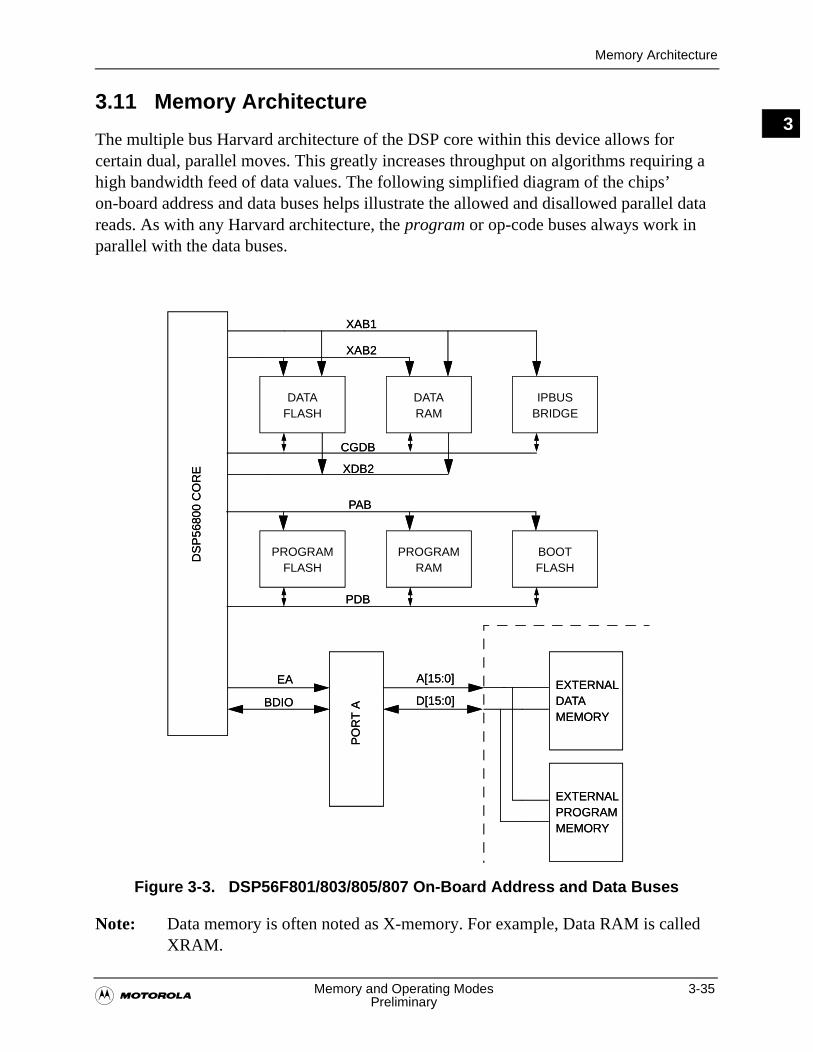
Memory Architecture
�Memory and Operating Modes 3-35
Preliminary
33.11 Memory Architecture
The multiple bus Harvard architecture of the DSP core within this device allows for certain dual, parallel moves. This greatly increases throughput on algorithms requiring a high bandwidth feed of data values. The following simplified diagram of the chips’ on-board address and data buses helps illustrate the allowed and disallowed parallel data reads. As with any Harvard architecture, the program or op-code buses always work in parallel with the data buses.
Figure 3-3. DSP56F801/803/805/807 On-Board Address and Data Buses
Note: Data memory is often noted as X-memory. For example, Data RAM is called XRAM.
BOOTFLASH
PROGRAMRAM
PROGRAMFLASH
IPBusBRIDGE
DATARAM
DATAFLASH
PO
RT
A
EXTERNALDATAMEMORY
EXTERNALPROGRAMMEMORY
DS
P56
800
CO
RE
XAB2
XAB1
CGDB
XDB2
PAB
PDB
EA
BDIO
A[15:0]
D[15:0]
BOOTFLASH
PROGRAMRAM
PROGRAMFLASH
IPBUSBRIDGE
DATARAM
DATAFLASH
PO
RT
A
EXTERNALDATAMEMORY
EXTERNALPROGRAMMEMORY
DS
P56
800
CO
RE
XAB2
XAB1
CGDB
XDB2
PAB
PDB
EA
BDIO
A[15:0]
D[15:0]
3-36 DSP56F801/803/805/807 User’s Manual�Preliminary
Memory Architecture
3The following data space reads are possible:
• Dual read XRAM using CGDB and XRAM using XDB2
• Dual read RAM using CGDB and XFLASH using XDB2
• Dual read XRAM using XDB2 and XFLASH using CGDB
• Single read XRAM using CGDB
• Single read XFLASH using CGDB
Note: Dual read XFLASH using XDB2 and XFLASH using CGDB is NOT allowed.
Dual reads solely from XFLASH are NOT allowed. CGDB reads and writes are a result of XAB1 addressing. XDB2 reads are a result of XAB2 addressing. Writes are NOT allowed. XAB2 addressing is always the second field of a dual move operation, and can only be sourced by the R3 register.
The XRAM is a true dual-port RAM. The XFLASH is not available as a dual-ported memory.
Note: Due to the IPBus methodology used for bussing from core to peripherals, the DSP56F801/803/805/807 does not connect the PGDB from the DSP core to the peripherals. There are certain addressing modes of the MOVE command that very likely cause a transfer to happen on the core’s Peripheral Global Data Bus (PGDB). The DSP56F801/803/805/807 does not connect the PGDB from the DSP core to the peripherals, so instructions such as MOVEP, utilizing this data bus, are not useful. The MOVEP instruction only functions for registers internal to the core: OnCE PGDB Bus Transfer Register (OPGDBR), Interrupt Priority Register (IPR) and Bus Control Register (BCR).
�Interrupt Controller (ITCN) 4-1
Preliminary
4
Chapter 4Interrupt Controller (ITCN)

4-2 DSP56F801/803/805/807 User’s Manual�Preliminary
4
Introduction
�Interrupt Controller (ITCN) 4-3
Preliminary
4
4.1 Introduction
The IPBus Interrupt Controller (ITCN) accepts Interrupt Request (IRQ) signals for Interrupt Priority (IP) Bus-based peripherals, assigns user-defined levels to each Interrupt Requests (IRQ), and then selects the highest pending IRQ for presentation to the DSP56800 core. The DSP56800 core includes circuitry supports with seven levels of interrupts. The DSP56800 gives priority to the interrupts associated with the highest level.
The ITCN augments the DSP56800 interrupt controller by expanding the maximum number of peripheral interrupts to 64 and adding the ability to assign each of the 64 interrupt request sources to one of the seven levels. Within any one of the seven levels, any number of interrupt sources may be assigned. Four additional information, refer to Figure 7-2, Interrupt Priority Register X$FFFB in the DSP56800 Family Manual.
Each interrupt source has a fixed vector number, regardless of the level it has been assigned. For any given level, its vector number determines an interrupt priority. The interrupt source with the highest vector has the highest priority within a given level.
The interrupt controller module does not mask, generate, or clear IRQs. The peripheral module issuing the IRQ defines the enabling and clearing methods of a particular interrupt. The interrupt controller provides only the priority assignments and the interrupt vector generation.
There are 64 3-bit Priority Level Registers (PLRs) specifying the level assignment, one to seven, for each interrupt request signal. Four PLRs are assembled together in each Group Priority Register (GPR). Each 16-bit GPR is capable of being read and accept writing. Each PLR value has a default value on reset, but the user, to suit the application’s need, may change each value. If a PLR value is set to zero, the effect is to disable that interrupt.
The ,��and ,� bits in the DSP56800 core Status Register (SR) determine the class of the permitted exceptions. To permit mask exceptions, , bits should be set to 01. To disable the mask exceptions, , bits should be set to 11. The Interrupt Priority Register (IPR), also part of the DSP56800 core, is located at its X$FFFB address. The IPR has an Interrupt Priority Level (IPL) bit assigned to each of the seven interrupt priority levels generated by the interrupt controller. Each IPL bit enables interrupts associated with its interrupt priority level.
Therefore, to enable a specific interrupt, the bit in the peripheral must be set, the PLR in the interrupt controller must be initialized and the corresponding IPL bit must be set in the processor status register.
The ITCN is designed for 64 interrupts; however, the DSP56F801/803/805/807 reserves the first 10 interrupt vectors for internally generated exceptions and the IRQA and IRQB external interrupts.
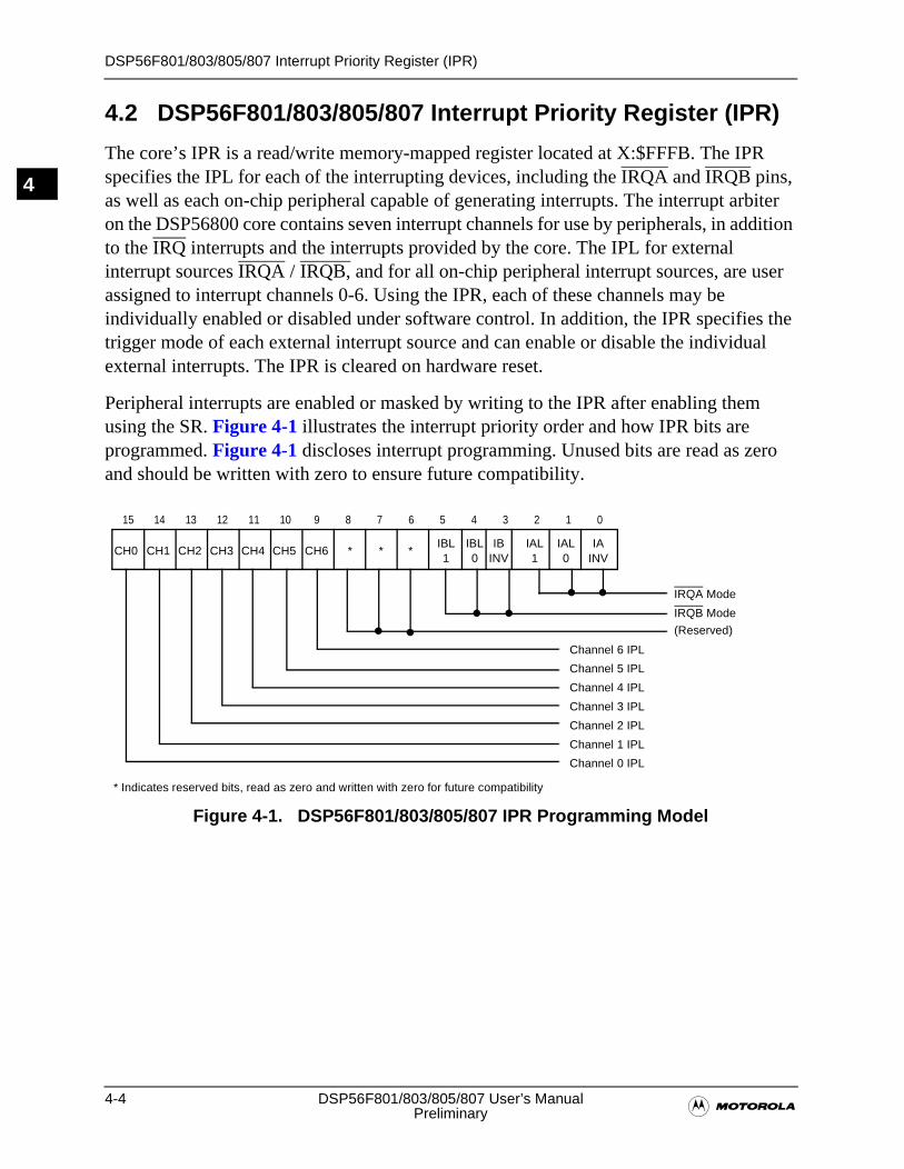
4-4 DSP56F801/803/805/807 User’s Manual�Preliminary
DSP56F801/803/805/807 Interrupt Priority Register (IPR)
4
4.2 DSP56F801/803/805/807 Interrupt Priority Register (IPR)
The core’s IPR is a read/write memory-mapped register located at X:$FFFB. The IPR specifies the IPL for each of the interrupting devices, including the IRQA and IRQB pins, as well as each on-chip peripheral capable of generating interrupts. The interrupt arbiter on the DSP56800 core contains seven interrupt channels for use by peripherals, in addition to the IRQ interrupts and the interrupts provided by the core. The IPL for external interrupt sources IRQA / IRQB, and for all on-chip peripheral interrupt sources, are user assigned to interrupt channels 0-6. Using the IPR, each of these channels may be individually enabled or disabled under software control. In addition, the IPR specifies the trigger mode of each external interrupt source and can enable or disable the individual external interrupts. The IPR is cleared on hardware reset.
Peripheral interrupts are enabled or masked by writing to the IPR after enabling them using the SR. Figure 4-1 illustrates the interrupt priority order and how IPR bits are programmed. Figure 4-1 discloses interrupt programming. Unused bits are read as zero and should be written with zero to ensure future compatibility.
Figure 4-1. DSP56F801/803/805/807 IPR Programming Model
* Indicates reserved bits, read as zero and written with zero for future compatibility
IRQA Mode
IRQB Mode
Channel 6 IPL
Channel 5 IPL
Channel 4 IPL
Channel 3 IPL
Channel 2 IPL
Channel 1 IPL
Channel 0 IPL
(Reserved)
CH0 CH1 CH2 CH3 CH4 CH5 CH6 * * *IBL IBL IAL IAL1 0 1 0
15 14 13 12 11 10 9 8 7 6 5 4 3 2 1 0
IB IAINV INV
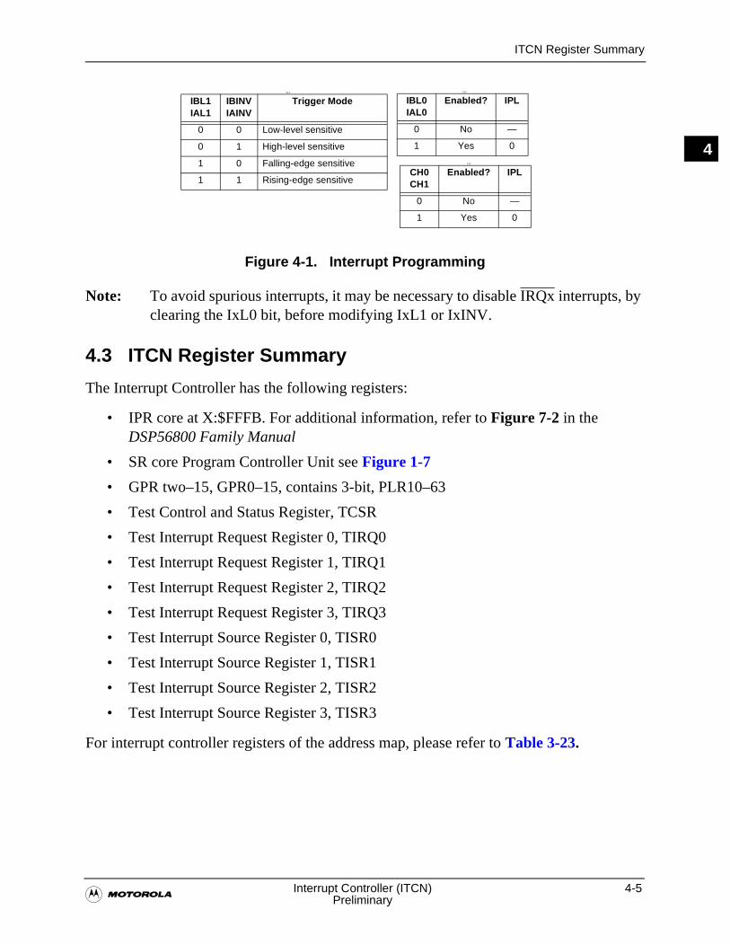
ITCN Register Summary
�Interrupt Controller (ITCN) 4-5
Preliminary
4
Figure 4-1. Interrupt Programming
Note: To avoid spurious interrupts, it may be necessary to disable IRQx interrupts, by clearing the IxL0 bit, before modifying IxL1 or IxINV.
4.3 ITCN Register Summary
The Interrupt Controller has the following registers:
• IPR core at X:$FFFB. For additional information, refer to Figure 7-2 in the DSP56800 Family Manual
• SR core Program Controller Unit see Figure 1-7
• GPR two–15, GPR0–15, contains 3-bit, PLR10–63
• Test Control and Status Register, TCSR
• Test Interrupt Request Register 0, TIRQ0
• Test Interrupt Request Register 1, TIRQ1
• Test Interrupt Request Register 2, TIRQ2
• Test Interrupt Request Register 3, TIRQ3
• Test Interrupt Source Register 0, TISR0
• Test Interrupt Source Register 1, TISR1
• Test Interrupt Source Register 2, TISR2
• Test Interrupt Source Register 3, TISR3
For interrupt controller registers of the address map, please refer to Table 3-23.
TST
IBL1IAL1
IBINVIAINV
Trigger Mode
0 0 Low-level sensitive
0 1 High-level sensitive
1 0 Falling-edge sensitive
1 1 Rising-edge sensitive
TST
IBL0IAL0
Enabled? IPL
0 No —
1 Yes 0
TST
CH0CH1
Enabled? IPL
0 No —
1 Yes 0
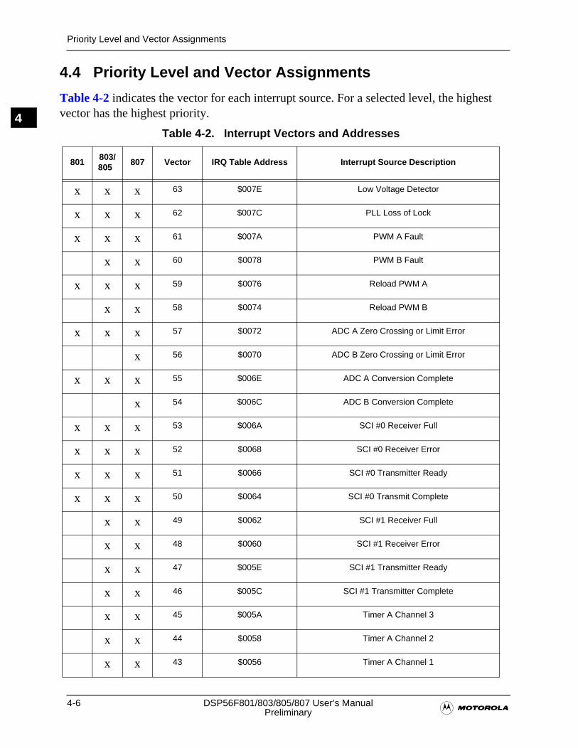
4-6 DSP56F801/803/805/807 User’s Manual�Preliminary
Priority Level and Vector Assignments
4
4.4 Priority Level and Vector Assignments
Table 4-2 indicates the vector for each interrupt source. For a selected level, the highest vector has the highest priority.
Table 4-2. Interrupt Vectors and Addresses
801803/805
807 Vector IRQ Table Address Interrupt Source Description
x x x 63 $007E Low Voltage Detector
x x x 62 $007C PLL Loss of Lock
x x x 61 $007A PWM A Fault
x x 60 $0078 PWM B Fault
x x x 59 $0076 Reload PWM A
x x 58 $0074 Reload PWM B
x x x 57 $0072 ADC A Zero Crossing or Limit Error
x 56 $0070 ADC B Zero Crossing or Limit Error
x x x 55 $006E ADC A Conversion Complete
x 54 $006C ADC B Conversion Complete
x x x 53 $006A SCI #0 Receiver Full
x x x 52 $0068 SCI #0 Receiver Error
x x x 51 $0066 SCI #0 Transmitter Ready
x x x 50 $0064 SCI #0 Transmit Complete
x x 49 $0062 SCI #1 Receiver Full
x x 48 $0060 SCI #1 Receiver Error
x x 47 $005E SCI #1 Transmitter Ready
x x 46 $005C SCI #1 Transmitter Complete
x x 45 $005A Timer A Channel 3
x x 44 $0058 Timer A Channel 2
x x 43 $0056 Timer A Channel 1
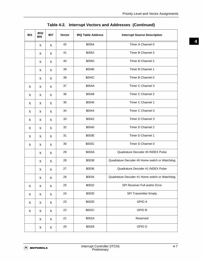
Priority Level and Vector Assignments
�Interrupt Controller (ITCN) 4-7
Preliminary
4x x 42 $0054 Timer A Channel 0
x x 41 $0052 Timer B Channel 3
x x 40 $0050 Timer B Channel 2
x x 39 $004E Timer B Channel 1
x x 38 $004C Timer B Channel 0
x x x 37 $004A Timer C Channel 3
x x x 36 $0048 Timer C Channel 2
x x x 35 $0046 Timer C Channel 1
x x x 34 $0044 Timer C Channel 0
x x x 33 $0042 Timer D Channel 3
x x x 32 $0040 Timer D Channel 2
x x x 31 $003E Timer D Channel 1
x x x 30 $003C Timer D Channel 0
x x 29 $003A Quadrature Decoder #0 INDEX Pulse
x x 28 $0038 Quadrature Decoder #0 Home switch or Watchdog
x x 27 $0036 Quadrature Decoder #1 INDEX Pulse
x x 26 $0034 Quadrature Decoder #1 Home switch or Watchdog
x x x 25 $0032 SPI Receiver Full and/or Error
x x x 24 $0030 SPI Transmitter Empty
x x x 23 $002E GPIO A
x x x 22 $002C GPIO B
x x 21 $002A Reserved
x x 20 $0028 GPIO D
Table 4-2. Interrupt Vectors and Addresses (Continued)
801803/805
807 Vector IRQ Table Address Interrupt Source Description
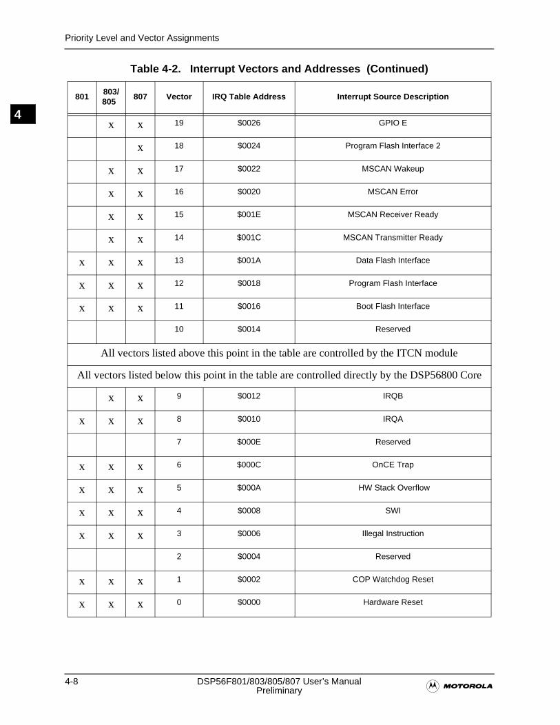
4-8 DSP56F801/803/805/807 User’s Manual�Preliminary
Priority Level and Vector Assignments
4x x 19 $0026 GPIO E
x 18 $0024 Program Flash Interface 2
x x 17 $0022 MSCAN Wakeup
x x 16 $0020 MSCAN Error
x x 15 $001E MSCAN Receiver Ready
x x 14 $001C MSCAN Transmitter Ready
x x x 13 $001A Data Flash Interface
x x x 12 $0018 Program Flash Interface
x x x 11 $0016 Boot Flash Interface
10 $0014 Reserved
All vectors listed above this point in the table are controlled by the ITCN module
All vectors listed below this point in the table are controlled directly by the DSP56800 Core
x x 9 $0012 IRQB
x x x 8 $0010 IRQA
7 $000E Reserved
x x x 6 $000C OnCE Trap
x x x 5 $000A HW Stack Overflow
x x x 4 $0008 SWI
x x x 3 $0006 Illegal Instruction
2 $0004 Reserved
x x x 1 $0002 COP Watchdog Reset
x x x 0 $0000 Hardware Reset
Table 4-2. Interrupt Vectors and Addresses (Continued)
801803/805
807 Vector IRQ Table Address Interrupt Source Description
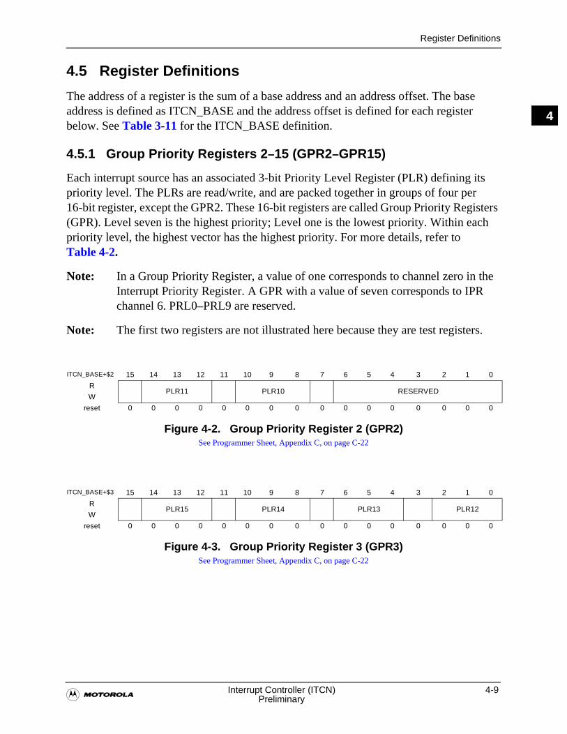
Register Definitions
�Interrupt Controller (ITCN) 4-9
Preliminary
4
4.5 Register Definitions
The address of a register is the sum of a base address and an address offset. The base address is defined as ITCN_BASE and the address offset is defined for each register below. See Table 3-11 for the ITCN_BASE definition.
4.5.1 Group Priority Registers 2–15 (GPR2–GPR15)
Each interrupt source has an associated 3-bit Priority Level Register (PLR) defining its priority level. The PLRs are read/write, and are packed together in groups of four per 16-bit register, except the GPR2. These 16-bit registers are called Group Priority Registers (GPR). Level seven is the highest priority; Level one is the lowest priority. Within each priority level, the highest vector has the highest priority. For more details, refer to Table 4-2.
Note: In a Group Priority Register, a value of one corresponds to channel zero in the Interrupt Priority Register. A GPR with a value of seven corresponds to IPR channel 6. PRL0–PRL9 are reserved.
Note: The first two registers are not illustrated here because they are test registers.
Figure 4-2. Group Priority Register 2 (GPR2)See Programmer Sheet, Appendix C, on page C-22
Figure 4-3. Group Priority Register 3 (GPR3)See Programmer Sheet, Appendix C, on page C-22
ITCN_BASE+$2 15 14 13 12 11 10 9 8 7 6 5 4 3 2 1 0
RPLR11 PLR10 RESERVED
W
reset 0 0 0 0 0 0 0 0 0 0 0 0 0 0 0 0
ITCN_BASE+$3 15 14 13 12 11 10 9 8 7 6 5 4 3 2 1 0
RPLR15 PLR14 PLR13 PLR12
W
reset 0 0 0 0 0 0 0 0 0 0 0 0 0 0 0 0
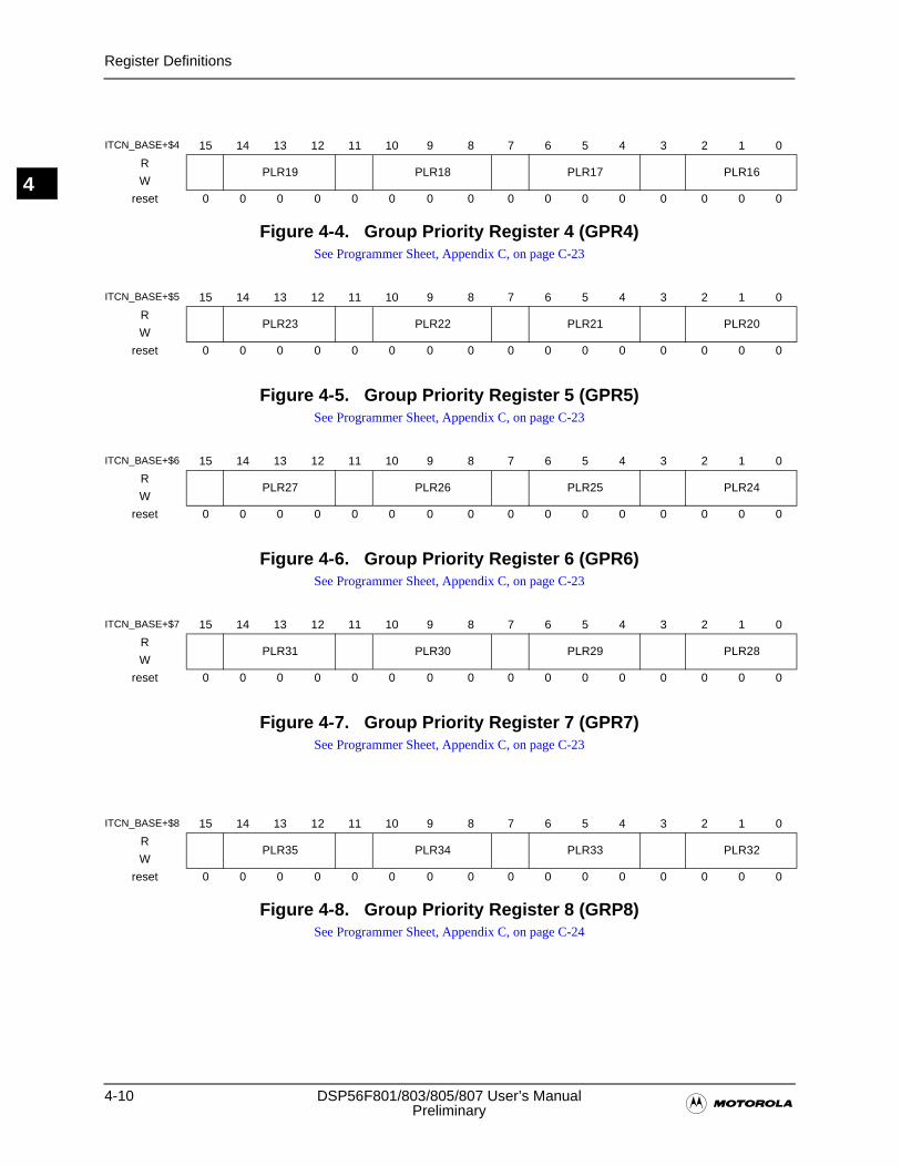
4-10 DSP56F801/803/805/807 User’s Manual�Preliminary
Register Definitions
4
Figure 4-4. Group Priority Register 4 (GPR4)See Programmer Sheet, Appendix C, on page C-23
Figure 4-5. Group Priority Register 5 (GPR5)See Programmer Sheet, Appendix C, on page C-23
Figure 4-6. Group Priority Register 6 (GPR6)See Programmer Sheet, Appendix C, on page C-23
Figure 4-7. Group Priority Register 7 (GPR7)See Programmer Sheet, Appendix C, on page C-23
Figure 4-8. Group Priority Register 8 (GRP8)See Programmer Sheet, Appendix C, on page C-24
ITCN_BASE+$4 15 14 13 12 11 10 9 8 7 6 5 4 3 2 1 0
RPLR19 PLR18 PLR17 PLR16
W
reset 0 0 0 0 0 0 0 0 0 0 0 0 0 0 0 0
ITCN_BASE+$5 15 14 13 12 11 10 9 8 7 6 5 4 3 2 1 0
RPLR23 PLR22 PLR21 PLR20
W
reset 0 0 0 0 0 0 0 0 0 0 0 0 0 0 0 0
ITCN_BASE+$6 15 14 13 12 11 10 9 8 7 6 5 4 3 2 1 0
RPLR27 PLR26 PLR25 PLR24
W
reset 0 0 0 0 0 0 0 0 0 0 0 0 0 0 0 0
ITCN_BASE+$7 15 14 13 12 11 10 9 8 7 6 5 4 3 2 1 0
RPLR31 PLR30 PLR29 PLR28
W
reset 0 0 0 0 0 0 0 0 0 0 0 0 0 0 0 0
ITCN_BASE+$8 15 14 13 12 11 10 9 8 7 6 5 4 3 2 1 0
RPLR35 PLR34 PLR33 PLR32
W
reset 0 0 0 0 0 0 0 0 0 0 0 0 0 0 0 0
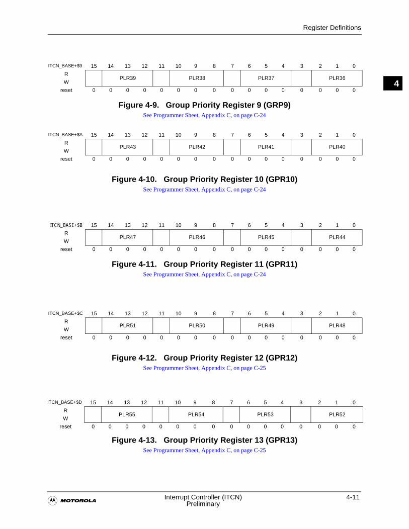
Register Definitions
�Interrupt Controller (ITCN) 4-11
Preliminary
4
Figure 4-9. Group Priority Register 9 (GRP9)See Programmer Sheet, Appendix C, on page C-24
Figure 4-10. Group Priority Register 10 (GPR10)See Programmer Sheet, Appendix C, on page C-24
Figure 4-11. Group Priority Register 11 (GPR11)See Programmer Sheet, Appendix C, on page C-24
Figure 4-12. Group Priority Register 12 (GPR12)See Programmer Sheet, Appendix C, on page C-25
Figure 4-13. Group Priority Register 13 (GPR13)See Programmer Sheet, Appendix C, on page C-25
ITCN_BASE+$9 15 14 13 12 11 10 9 8 7 6 5 4 3 2 1 0
RPLR39 PLR38 PLR37 PLR36
W
reset 0 0 0 0 0 0 0 0 0 0 0 0 0 0 0 0
ITCN_BASE+$A 15 14 13 12 11 10 9 8 7 6 5 4 3 2 1 0
RPLR43 PLR42 PLR41 PLR40
W
reset 0 0 0 0 0 0 0 0 0 0 0 0 0 0 0 0
ITCN_BASE+$B 15 14 13 12 11 10 9 8 7 6 5 4 3 2 1 0
RPLR47 PLR46 PLR45 PLR44
W
reset 0 0 0 0 0 0 0 0 0 0 0 0 0 0 0 0
ITCN_BASE+$C 15 14 13 12 11 10 9 8 7 6 5 4 3 2 1 0
RPLR51 PLR50 PLR49 PLR48
W
reset 0 0 0 0 0 0 0 0 0 0 0 0 0 0 0 0
ITCN_BASE+$D 15 14 13 12 11 10 9 8 7 6 5 4 3 2 1 0
RPLR55 PLR54 PLR53 PLR52
W
reset 0 0 0 0 0 0 0 0 0 0 0 0 0 0 0 0
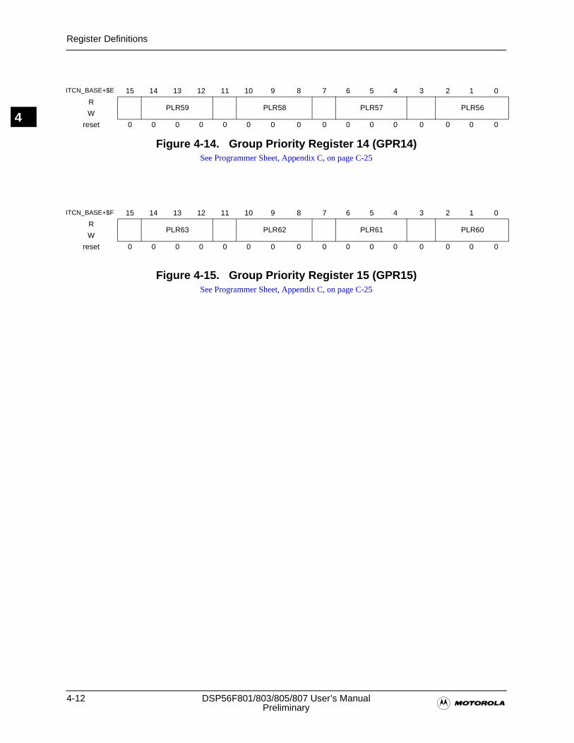
4-12 DSP56F801/803/805/807 User’s Manual�Preliminary
Register Definitions
4
Figure 4-14. Group Priority Register 14 (GPR14)See Programmer Sheet, Appendix C, on page C-25
Figure 4-15. Group Priority Register 15 (GPR15)See Programmer Sheet, Appendix C, on page C-25
ITCN_BASE+$E 15 14 13 12 11 10 9 8 7 6 5 4 3 2 1 0
RPLR59 PLR58 PLR57 PLR56
W
reset 0 0 0 0 0 0 0 0 0 0 0 0 0 0 0 0
ITCN_BASE+$F 15 14 13 12 11 10 9 8 7 6 5 4 3 2 1 0
RPLR63 PLR62 PLR61 PLR60
W
reset 0 0 0 0 0 0 0 0 0 0 0 0 0 0 0 0
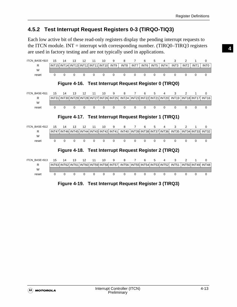
Register Definitions
�Interrupt Controller (ITCN) 4-13
Preliminary
4
4.5.2 Test Interrupt Request Registers 0-3 (TIRQO-TIQ3)
Each low active bit of these read-only registers display the pending interrupt requests to the ITCN module. INT = interrupt with corresponding number. (TIRQ0–TIRQ3 registers are used in factory testing and are not typically used in applications.
Figure 4-16. Test Interrupt Request Register 0 (TIRQ0)
Figure 4-17. Test Interrupt Request Register 1 (TIRQ1)
Figure 4-18. Test Interrupt Request Register 2 (TIRQ2)
Figure 4-19. Test Interrupt Request Register 3 (TIRQ3)
ITCN_BASE+$10 15 14 13 12 11 10 9 8 7 6 5 4 3 2 1 0
R INT15 INT14 INT13 INT12 INT11 INT10 INT9 INT8 INT7 INT6 INT5 INT4 INT3 INT2 INT1 INT0
W
reset 0 0 0 0 0 0 0 0 0 0 0 0 0 0 0 0
ITCN_BASE+$11 15 14 13 12 11 10 9 8 7 6 5 4 3 2 1 0
R INT31 INT30 INT29 INT28 INT27 INT26 INT25 INT24 INT23 INT22 INT21 INT20 INT19 INT18 INT17 INT16
W
reset 0 0 0 0 0 0 0 0 0 0 0 0 0 0 0 0
ITCN_BASE+$12 15 14 13 12 11 10 9 8 7 6 5 4 3 2 1 0
R INT47 INT46 INT45 INT44 INT43 INT42 INT41 INT40 INT39 INT38 INT37 INT36 INT35 INT34 INT33 INT32
W
reset 0 0 0 0 0 0 0 0 0 0 0 0 0 0 0 0
ITCN_BASE+$13 15 14 13 12 11 10 9 8 7 6 5 4 3 2 1 0
R INT63 INT62 INT61 INT60 INT59 INT58 INT57 INT56 INT55 INT54 INT53 INT52 INT51 INT50 INT49 INT48
W
reset 0 0 0 0 0 0 0 0 0 0 0 0 0 0 0 0
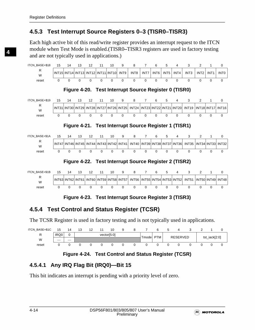
4-14 DSP56F801/803/805/807 User’s Manual�Preliminary
Register Definitions
4
4.5.3 Test Interrupt Source Registers 0–3 (TISR0–TISR3)
Each high active bit of this read/write register provides an interrupt request to the ITCN module when Test Mode is enabled.(TISR0–TISR3 registers are used in factory testing and are not typically used in applications.)
Figure 4-20. Test Interrupt Source Register 0 (TISR0)
Figure 4-21. Test Interrupt Source Register 1 (TISR1)
Figure 4-22. Test Interrupt Source Register 2 (TISR2)
Figure 4-23. Test Interrupt Source Register 3 (TISR3)
4.5.4 Test Control and Status Register (TCSR)
The TCSR Register is used in factory testing and is not typically used in applications.
Figure 4-24. Test Control and Status Register (TCSR)
4.5.4.1 Any IRQ Flag Bit (IRQ0)—Bit 15
This bit indicates an interrupt is pending with a priority level of zero.
ITCN_BASE+$18 15 14 13 12 11 10 9 8 7 6 5 4 3 2 1 0
RINT15 INT14 INT13 INT12 INT11 INT10 INT9 INT8 INT7 INT6 INT5 INT4 INT3 INT2 INT1 INT0
W
reset 0 0 0 0 0 0 0 0 0 0 0 0 0 0 0 0
ITCN_BASE+$19 15 14 13 12 11 10 9 8 7 6 5 4 3 2 1 0
RINT31 INT30 INT29 INT28 INT27 INT26 INT25 INT24 INT23 INT22 INT21 INT20 INT19 INT18 INT17 INT16
W
reset 0 0 0 0 0 0 0 0 0 0 0 0 0 0 0 0
ITCN_BASE+$1A 15 14 13 12 11 10 9 8 7 6 5 4 3 2 1 0
RINT47 INT46 INT45 INT44 INT43 INT42 INT41 INT40 INT39 INT38 INT37 INT36 INT35 INT34 INT33 INT32
W
reset 0 0 0 0 0 0 0 0 0 0 0 0 0 0 0 0
ITCN_BASE+$1B 15 14 13 12 11 10 9 8 7 6 5 4 3 2 1 0
RINT63 INT62 INT61 INT60 INT59 INT58 INT57 INT56 INT55 INT54 INT53 INT52 INT51 INT50 INT49 INT48
W
reset 0 0 0 0 0 0 0 0 0 0 0 0 0 0 0 0
ITCN_BASE+$1C 15 14 13 12 11 10 9 8 7 6 5 4 3 2 1 0
R IRQ0 0 vector[5:0]Tmode PTM RESERVED tst_iack[2:0]
W — —
reset 0 0 0 0 0 0 0 0 0 0 0 0 0 0 0 0
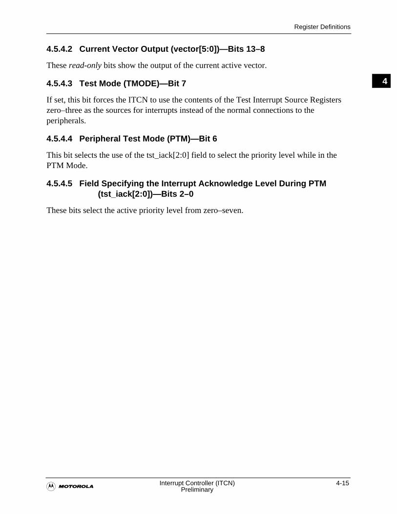
Register Definitions
�Interrupt Controller (ITCN) 4-15
Preliminary
4
4.5.4.2 Current Vector Output (vector[5:0])—Bits 13–8
These read-only bits show the output of the current active vector.
4.5.4.3 Test Mode (TMODE)—Bit 7
If set, this bit forces the ITCN to use the contents of the Test Interrupt Source Registers zero–three as the sources for interrupts instead of the normal connections to the peripherals.
4.5.4.4 Peripheral Test Mode (PTM)—Bit 6
This bit selects the use of the tst_iack[2:0] field to select the priority level while in the PTM Mode.
4.5.4.5 Field Specifying the Interrupt Acknowledge Level During PTM (tst_iack[2:0])—Bits 2–0
These bits select the active priority level from zero–seven.

4-16 DSP56F801/803/805/807 User’s Manual�Preliminary
Register Definitions
4

�Flash Memory Interface 5-1
Preliminary
5Chapter 5Flash Memory Interface

5-2 DSP56F801/803/805/807 User’s Manual�Preliminary
5
Register Summary
�Flash Memory Interface 5-3
Preliminary
5
5.1 Introduction
Flash memory provides reliable, non-volatile memory storage, thereby eliminating required external storage devices. Its software is easily programmable and it can be booted directly from Flash. Memory updating is also a simple process using either Flash memories through SPI, SCI, or OnCETM, described in Chapter 17.
5.2 Features• Endurance: 100,000 Cycles (typical)
• Memory Organization for DSP56F801
— Program Flash = 8K × 16
— Data Flash = 2K × 16
— Boot Flash = 2K × 16
• Memory Organization for DSP56F803 and DSP56F805
— Program Flash = 32K × 16 + 64 × 16
— Data Flash = 4K × 16 + 64 × 16
— Boot Flash = 2K × 16 + 64 × 16Memory Organization for DSP56F807
— Program Flash = 64K × 16 + 64 × 16
— Data Flash = 8K × 16 + 64 × 16
— Boot Flash = 2K × 16 + 64 × 16
• Page Erase Capability: 512 bytes per page
• Block (Mass) Erase Capability
• Access Time: 20 ns (max)
• Word (16-bit) Program Time: 20 µs(min)
• Page Erase Time: 40 ms (min)
• Mass Erase Time: 100 ms (min)
5.3 Register Summary
The interface also block-write protects all Flash registers except the active one. The Flash interface units are the same for Program Flash Interface Unit (PFIU). Since the DSP56 F807 has 64K of Program Flash, 60K are usable while 4K is reserved, an extra Program Flash Interface Unit (PFIU2) is required to access the second half of the Flash.
5-4 DSP56F801/803/805/807 User’s Manual�Preliminary
Register Summary
5
A prefix is added to each register for reflect PFIU, Data Flash Interface Unit (DFIU), and Boot Flash Interface Unit (BFIU). For each Flash Interface Unit (FIU) the corresponding letter P for program, D for data, or B for boot must be included in front of the FIU in both the register name and base address. For example, the FIU_CNTL definition is same for PFIU_CNTL at memory location PFUI_BASE+0, DFIU_CNTL at memory location DFUI_BASE+0, and BFIU_CNTL at memory location BFUI_BASE+0.
Note: Since the DSP56F807 has 60K Program Flash, two Program Flash Interface Units are required to reach all 60K memory locations. As a result, the DSP56F807 has a second set of PFIU registers beginning with memory location PFIU2_BASE, defined in Section 3.11. The second Program Flash Interface Unit (PFIU2) functions the same as the original PFIU. For the DSP56F807, PFIU controls the first half of Program Flash and PFIU2 controls the last half of Program Flash.
Each Flash Integration Unit has the following registers.
• Flash Control Register (FIU_CNTL)
• Flash Program Enable Register (FIU_PE)
• Flash Erase Enable Register (FIU_EE)
• Flash Address Register (FIU_ADDR)
• Flash Data Register (FIU_DATA)
• Flash Interrupt Enable Register (FIU_IE)
• Flash Interrupt Source Register (FIU_IS)
• Flash Interrupt Pending Register (FIU_IP)
• Flash Clock Divisor Register (FIU_CKDIVISOR)
• Flash Terase Limit Register (FIU_TERASEL)
• Flash Tme Limit Register (FIU_TMEL)
• Flash Tnvs Limit Register (FIU_TNVSL)
• Flash Tpgs Limit Register (FIU_TPGSL)
• Flash Tprog Limit Register (FIU_TPROGL)
• Flash Tnvh Limit Register (FIU_TNVHL)
• Flash Tnvh1 Limit Register (FIU_TNVH1L)
• Flash Trcv Limit Register (FIU_TRCVL)
For more information on PFIU registers please refer to Table 3-30. Please refer to
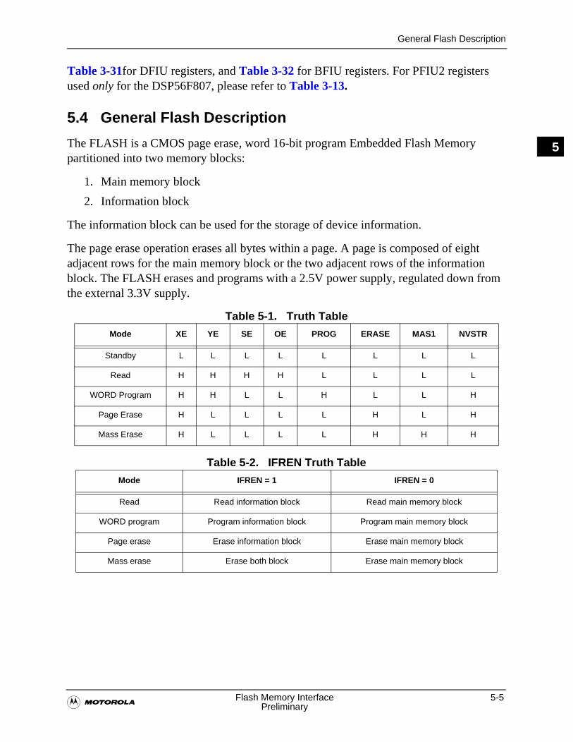
General Flash Description
�Flash Memory Interface 5-5
Preliminary
5
Table 3-31for DFIU registers, and Table 3-32 for BFIU registers. For PFIU2 registers used only for the DSP56F807, please refer to Table 3-13.
5.4 General Flash Description
The FLASH is a CMOS page erase, word 16-bit program Embedded Flash Memory partitioned into two memory blocks:
1. Main memory block
2. Information block
The information block can be used for the storage of device information.
The page erase operation erases all bytes within a page. A page is composed of eight adjacent rows for the main memory block or the two adjacent rows of the information block. The FLASH erases and programs with a 2.5V power supply, regulated down from the external 3.3V supply.
Table 5-1. Truth Table
Table 5-2. IFREN Truth Table
Mode XE YE SE OE PROG ERASE MAS1 NVSTR
Standby L L L L L L L L
Read H H H H L L L L
WORD Program H H L L H L L H
Page Erase H L L L L H L H
Mass Erase H L L L L H H H
Mode IFREN = 1 IFREN = 0
Read Read information block Read main memory block
WORD program Program information block Program main memory block
Page erase Erase information block Erase main memory block
Mass erase Erase both block Erase main memory block
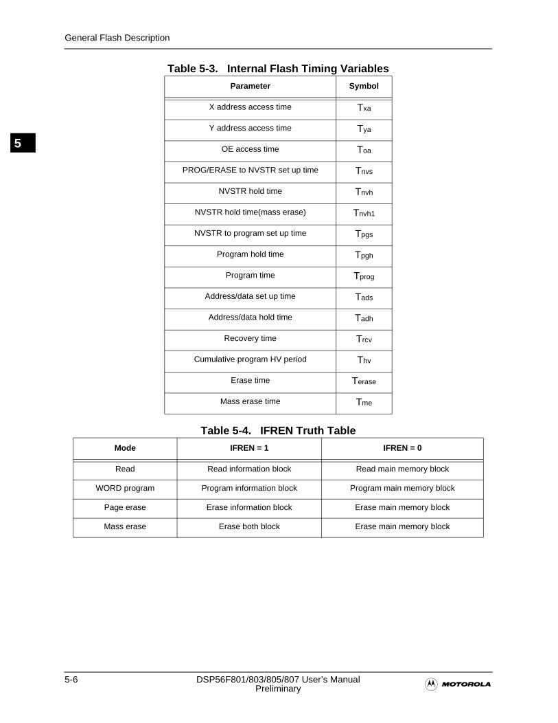
5-6 DSP56F801/803/805/807 User’s Manual�Preliminary
General Flash Description
5
Table 5-3. Internal Flash Timing Variables
Table 5-4. IFREN Truth Table
Parameter Symbol
X address access time Txa
Y address access time Tya
OE access time Toa
PROG/ERASE to NVSTR set up time Tnvs
NVSTR hold time Tnvh
NVSTR hold time(mass erase) Tnvh1
NVSTR to program set up time Tpgs
Program hold time Tpgh
Program time Tprog
Address/data set up time Tads
Address/data hold time Tadh
Recovery time Trcv
Cumulative program HV period Thv
Erase time Terase
Mass erase time Tme
Mode IFREN = 1 IFREN = 0
Read Read information block Read main memory block
WORD program Program information block Program main memory block
Page erase Erase information block Erase main memory block
Mass erase Erase both block Erase main memory block
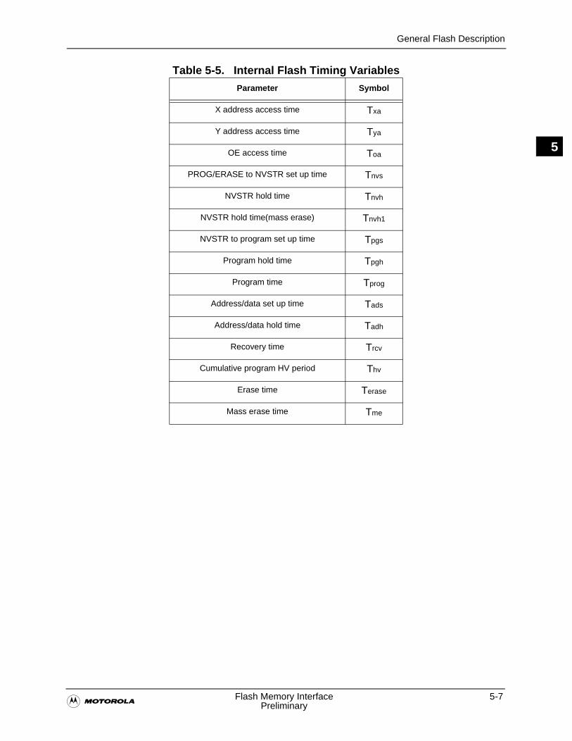
General Flash Description
�Flash Memory Interface 5-7
Preliminary
5
Table 5-5. Internal Flash Timing Variables
Parameter Symbol
X address access time Txa
Y address access time Tya
OE access time Toa
PROG/ERASE to NVSTR set up time Tnvs
NVSTR hold time Tnvh
NVSTR hold time(mass erase) Tnvh1
NVSTR to program set up time Tpgs
Program hold time Tpgh
Program time Tprog
Address/data set up time Tads
Address/data hold time Tadh
Recovery time Trcv
Cumulative program HV period Thv
Erase time Terase
Mass erase time Tme
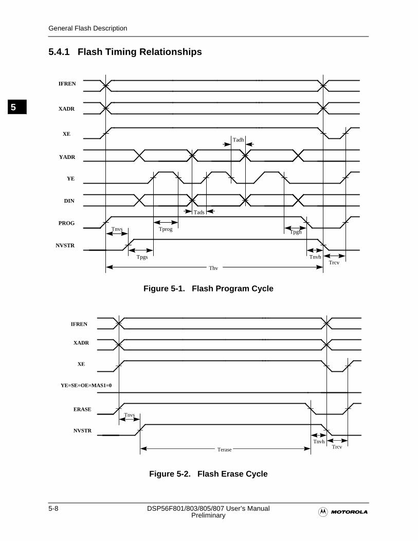
5-8 DSP56F801/803/805/807 User’s Manual�Preliminary
General Flash Description
5
5.4.1 Flash Timing Relationships
Figure 5-1. Flash Program Cycle
Figure 5-2. Flash Erase Cycle
XADR
YADR
YE
DIN
PROG
NVSTR
Tnvs
Tpgs
Tadh
Tprog
Tads
Tpgh
TnvhTrcv
Thv
IFREN
XE
XADR
YE=SE=OE=MAS1=0
ERASE
NVSTR
Tnvs
TnvhTrcvTerase
IFREN
XE
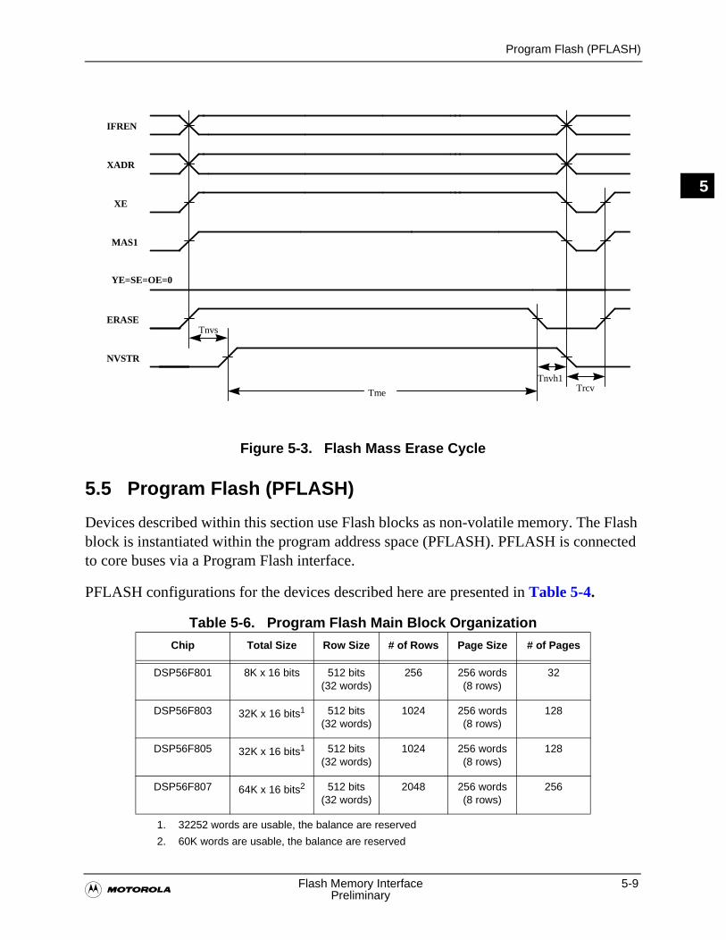
Program Flash (PFLASH)
�Flash Memory Interface 5-9
Preliminary
5
Figure 5-3. Flash Mass Erase Cycle
5.5 Program Flash (PFLASH)
Devices described within this section use Flash blocks as non-volatile memory. The Flash block is instantiated within the program address space (PFLASH). PFLASH is connected to core buses via a Program Flash interface.
PFLASH configurations for the devices described here are presented in Table 5-4.
Table 5-6. Program Flash Main Block Organization
Chip Total Size Row Size # of Rows Page Size # of Pages
DSP56F801 8K x 16 bits 512 bits(32 words)
256 256 words(8 rows)
32
DSP56F803 32K x 16 bits1
1. 32252 words are usable, the balance are reserved
512 bits(32 words)
1024 256 words(8 rows)
128
DSP56F805 32K x 16 bits1 512 bits(32 words)
1024 256 words(8 rows)
128
DSP56F807 64K x 16 bits2
2. 60K words are usable, the balance are reserved
512 bits(32 words)
2048 256 words(8 rows)
256
XADR
YE=SE=OE=0
ERASE
NVSTR
Tnvs
Tnvh1TrcvTme
MAS1
IFREN
XE
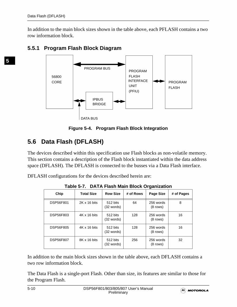
5-10 DSP56F801/803/805/807 User’s Manual�Preliminary
Data Flash (DFLASH)
5
In addition to the main block sizes shown in the table above, each PFLASH contains a two row information block.
5.5.1 Program Flash Block Diagram
Figure 5-4. Program Flash Block Integration
5.6 Data Flash (DFLASH)
The devices described within this specification use Flash blocks as non-volatile memory. This section contains a description of the Flash block instantiated within the data address space (DFLASH). The DFLASH is connected to the busses via a Data Flash interface.
DFLASH configurations for the devices described herein are:
Table 5-7. DATA Flash Main Block Organization
In addition to the main block sizes shown in the table above, each DFLASH contains a two row information block.
The Data Flash is a single-port Flash. Other than size, its features are similar to those for the Program Flash.
Chip Total Size Row Size # of Rows Page Size # of Pages
DSP56F801 2K x 16 bits 512 bits(32 words)
64 256 words(8 rows)
8
DSP56F803 4K x 16 bits 512 bits(32 words)
128 256 words(8 rows)
16
DSP56F805 4K x 16 bits 512 bits(32 words)
128 256 words(8 rows)
16
DSP56F807 8K x 16 bits 512 bits(32 words)
256 256 words(8 rows)
32
IPBUSBRIDGE
PROGRAM
INTERFACEUNIT
PROGRAM
56800
PROGRAM BUS
DATA BUS
FLASH
(PFIU)FLASH
CORE
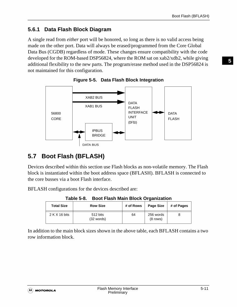
Boot Flash (BFLASH)
�Flash Memory Interface 5-11
Preliminary
5
5.6.1 Data Flash Block Diagram
A single read from either port will be honored, so long as there is no valid access being made on the other port. Data will always be erased/programmed from the Core Global Data Bus (CGDB) regardless of mode. These changes ensure compatibility with the code developed for the ROM-based DSP56824, where the ROM sat on xab2/xdb2, while giving additional flexibility to the new parts. The program/erase method used in the DSP56824 is not maintained for this configuration.
Figure 5-5. Data Flash Block Integration
5.7 Boot Flash (BFLASH)
Devices described within this section use Flash blocks as non-volatile memory. The Flash block is instantiated within the boot address space (BFLASH). BFLASH is connected to the core busses via a boot Flash interface.
BFLASH configurations for the devices described are:
Table 5-8. Boot Flash Main Block Organization
In addition to the main block sizes shown in the above table, each BFLASH contains a two row information block.
Total Size Row Size # of Rows Page Size # of Pages
2 K X 16 bits 512 bits(32 words)
64 256 words(8 rows)
8
IPBUSBRIDGE
FLASHINTERFACEUNIT
DATA
XAB1 BUS
XAB2 BUS
DATA BUS
DATA
56800
CORE(DFIU)
FLASH
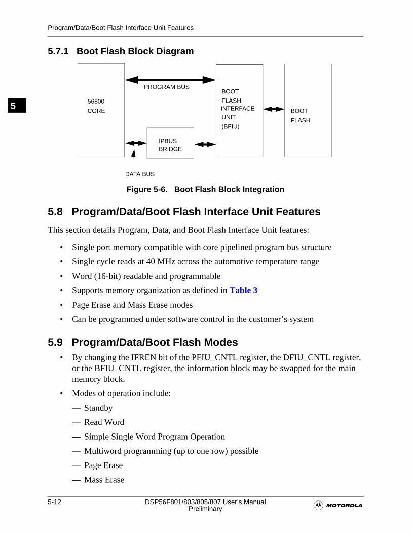
5-12 DSP56F801/803/805/807 User’s Manual�Preliminary
Program/Data/Boot Flash Interface Unit Features
5
5.7.1 Boot Flash Block Diagram
Figure 5-6. Boot Flash Block Integration
5.8 Program/Data/Boot Flash Interface Unit Features
This section details Program, Data, and Boot Flash Interface Unit features:
• Single port memory compatible with core pipelined program bus structure
• Single cycle reads at 40 MHz across the automotive temperature range
• Word (16-bit) readable and programmable
• Supports memory organization as defined in Table 3
• Page Erase and Mass Erase modes
• Can be programmed under software control in the customer’s system
5.9 Program/Data/Boot Flash Modes• By changing the IFREN bit of the PFIU_CNTL register, the DFIU_CNTL register,
or the BFIU_CNTL register, the information block may be swapped for the main memory block.
• Modes of operation include:
— Standby
— Read Word
— Simple Single Word Program Operation
— Multiword programming (up to one row) possible
— Page Erase
— Mass Erase
IPBUSBRIDGE
BOOT
INTERFACEUNIT
BOOT
56800
PROGRAM BUS
DATA BUS
FLASH
(BFIU)FLASH
CORE
Functional Description of the PFIU, DFIU and BFIU
�Flash Memory Interface 5-13
Preliminary
5
• The PFLASH, DFLASH or BFLASH is automatically put in Standby mode when not being read, programmed or erased
• Reads are disabled during Program/Erase operations
• Interrupts are individually maskable
• An interrupt will be generated for
— Reads out of range (trying to access a row past the first two in the information block)
— Read attempted during program
— Read attempted during erase
— Any of seven internal timer timeouts used during program/erase operations
• Intelligent erase and word programming features
5.10 Functional Description of the PFIU, DFIU and BFIU• The PFIU, DFIU and BFIU have internal timers for
— Tnvs represents PROG/ERASE to NVSTR setup time
— Tnvh and Tnvh1 represent NVSTR hold times
— Tpgs represents NVSTR to program setup time
— Tprog represents Program time
— Trec represents Recovery time
— Terase represents Erase time
— Tme represents Mass Erase time
• These are initialized upon reset to default values expected to work correctly for word programming and page erase operations. They may be overwritten by application code after reset if it is necessary to tweak operation based upon Flash characterization data
• All read/program/erase functions are terminated by a system reset
• The Flash will automatically be put in Standby mode when not being accessed
• During an erase cycle, all bits within the affected area are changed to one. Programming a bit results in it being changed to zero. Bits can only be changed back to one by erasing that section of memory again. A bit cannot be programmed to one

5-14 DSP56F801/803/805/807 User’s Manual�Preliminary
Flash Programming and Erase Models
5
5.11 Flash Programming and Erase Models
Please refer to figures in Section 5.4 for flash timing relationships required in the following intelligent word, dumb word programming, and intelligent erase operation.
The recommended flash programming mode is the Intelligent Word Programming, as described in Section 5.11.1. Although the Dumb Word Programming is described in Section 5.11.2, it is not the preferred method of programming the flash and it is not recommended.
5.11.1 Intelligent Word Programming
Assuming the word in question has already been erased, a single 16-bit word may be programmed through the following method:
1. Start with the Flash in either Standby or Read mode. Read FIU_CNTL register to insure this is true. All bits should be clear with the exception of IFREN. It may be set. See Section 5.10.
2. Enable programming by setting the IPE bit and row number in the FIU_PE register. To calculate the row number, use the following algorithm:
— Target_Address AND $7FFF divided by $20=ROW
— Or put differently, set the MSB of the target address to zero and right shift the result five place
3. Set the IE[8] bit in the FIU_IE register to enable to Trcv interrupt if desired to flag completion of programming.
4. Write the value desired to the proper word in the Flash memory map. Note a single location in the Flash may map to different locations in the memory map based upon the mode selected on startup. The FIU will adjust accordingly. This write to the Flash memory map, while the IPE bit is set, will start the internal state machine to run the Flash through its programming paces.
5. Do not attempt to access the Flash again until the BUSY signal clears in the FIU_CNTL register, corresponding to the Trcv interrupt when enabled.
6. When completed programming words, be certain to clear the IPE bit in the FIU_PE register.
The intelligent programming feature can only program one word at a time. Multiple words may be programmed by repeating the process, or by switching to the Dumb Word Programming method, outlined below.
Flash Programming and Erase Models
�Flash Memory Interface 5-15
Preliminary
5
5.11.2 Dumb Word Programming
The Flash allows programming of one or more words in a row. Assuming the words in question have already been erased, 16-bit words may be programmed via the following method:
1. Start with the Flash in either Standby or Read mode. Read the BUSY bit in the FIU_CNTL register ensuring it is clear
2. Enable programming by setting the DPE bit and row number in the FIU_PE register
3. Write the value you wish to the desired word in the Flash memory space. IS[0] must be clear before proceeding
4. Set the XE and PROG bits in the FIU_CNTL register
5. Delay for Tnvs
6. Set the NVSTR bit in the FIU_CNTL register
7. Delay for Tpgs
8. Set the YE bit in the FIU_CNTL register
9. Delay for Tprog
10. Clear the YE bit in the FIU_CNTL register
11. By writing to another location in the Flash memory space, update the values in FIU_ADDR and FIU_DATA if additional words are required, then loop back to step eight above. Address changes must be limited to within a single row. IS[0] must be clear before proceeding. Attempts to change the FIU_CNTL register with IS[0] set will have no effect.
12. Clear the PROG bit in the FIU_CNTL register, must be a separate step from clearing YE
13. Delay for Tnvh
14. Clear the NVSTR and XE bits in the FIU_CNTL register
15. Delay for Trcv
The Flash cannot be accessed directly when the process above is underway. The program code for changing the Program Flash contents must be executing from some other memory, either external ROM/RAM or internal Program RAM.
The FIU timer registers cannot be used to generate interrupts for each of the delays above. If interrupts are desired to generate the timing breakpoints for the dumb programming process they must be generated from some other timing or interrupt source.
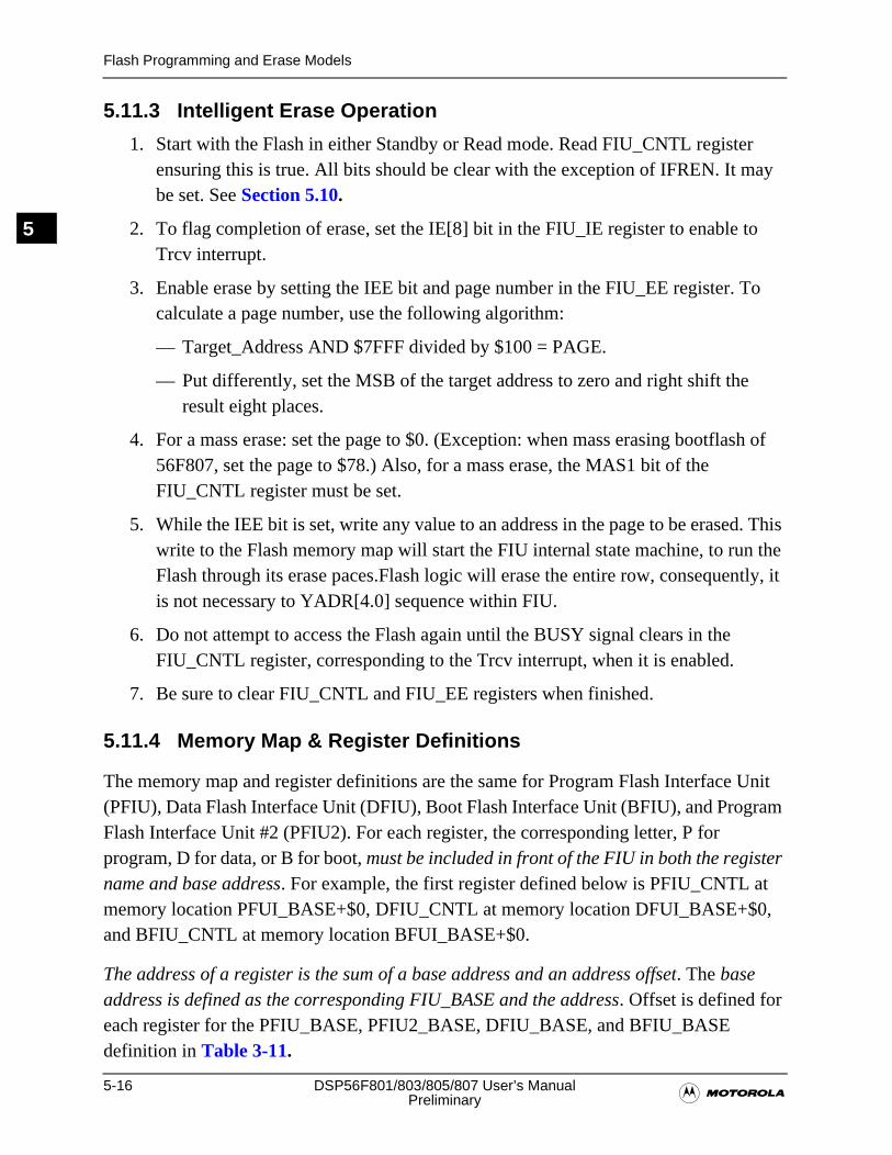
5-16 DSP56F801/803/805/807 User’s Manual�Preliminary
Flash Programming and Erase Models
5
5.11.3 Intelligent Erase Operation
1. Start with the Flash in either Standby or Read mode. Read FIU_CNTL register ensuring this is true. All bits should be clear with the exception of IFREN. It may be set. See Section 5.10.
2. To flag completion of erase, set the IE[8] bit in the FIU_IE register to enable to Trcv interrupt.
3. Enable erase by setting the IEE bit and page number in the FIU_EE register. To calculate a page number, use the following algorithm:
— Target_Address AND $7FFF divided by $100 = PAGE.
— Put differently, set the MSB of the target address to zero and right shift the result eight places.
4. For a mass erase: set the page to $0. (Exception: when mass erasing bootflash of 56F807, set the page to $78.) Also, for a mass erase, the MAS1 bit of the FIU_CNTL register must be set.
5. While the IEE bit is set, write any value to an address in the page to be erased. This write to the Flash memory map will start the FIU internal state machine, to run the Flash through its erase paces.Flash logic will erase the entire row, consequently, it is not necessary to YADR[4.0] sequence within FIU.
6. Do not attempt to access the Flash again until the BUSY signal clears in the FIU_CNTL register, corresponding to the Trcv interrupt, when it is enabled.
7. Be sure to clear FIU_CNTL and FIU_EE registers when finished.
5.11.4 Memory Map & Register Definitions
The memory map and register definitions are the same for Program Flash Interface Unit (PFIU), Data Flash Interface Unit (DFIU), Boot Flash Interface Unit (BFIU), and Program Flash Interface Unit #2 (PFIU2). For each register, the corresponding letter, P for program, D for data, or B for boot, must be included in front of the FIU in both the register name and base address. For example, the first register defined below is PFIU_CNTL at memory location PFUI_BASE+$0, DFIU_CNTL at memory location DFUI_BASE+$0, and BFIU_CNTL at memory location BFUI_BASE+$0.
The address of a register is the sum of a base address and an address offset. The base address is defined as the corresponding FIU_BASE and the address. Offset is defined for each register for the PFIU_BASE, PFIU2_BASE, DFIU_BASE, and BFIU_BASE definition in Table 3-11.

Flash Programming and Erase Models
�Flash Memory Interface 5-17
Preliminary
5
5.11.4.1 Flash Control Register (FIU_CNTL)
When busy is asserted in intelligent programming mode, all the registers cannot be written. In dumb programming mode, only the address and data registers can be written.
Figure 5-7. Flash Control Register (FIU_CNTL)See Programmer Sheet, Appendix C, on page C-26
5.11.4.1.1 Busy Bit (BUSY)—Bit 15
When the busy bit is asserted in intelligent programming mode, all the registers cannot be written. In dumb programming mode, only the address and data registers can be written.
5.11.4.1.2 Reserved Bits—Bits 14–7
These reserved bits cannot be modified. They are read as zero.
5.11.4.1.3 Information Block Enable Bit (IFREN)—Bit 6
When IFREN is asserted, the information block of the Flash is enabled. The bit permits write in all modes when the BUSY bit is clear. The IFREN bit has the following effect.
This bit enables the X address when asserted. It can be written only in Dumb Programming mode when the IS[0] bit is clear; read only in Intelligent Programming mode to reflect the state of the Flash XE pin.
The IFREN Bit has the following effect: X Address Enable Bit (XE)—Bit 5
5.11.4.1.4 Y Address Enable Bit (YE)—Bit 4
This bit enables the Y address when asserted. It can be written only in Dumb Programming mode when the IS[0] bit is clear; read only in Intelligent Programming mode to reflect the state of the Flash YE pin.
FIU_BASE+$0 15 14 13 12 11 10 9 8 7 6 5 4 3 2 1 0
R BUSY 0 0 0 0 0 0 0 0IFREN XE YE PROG ERASE MAS1 NVSTR
W
reset 0 0 0 0 0 0 0 0 0 0 0 0 0 0 0 0
Table 5-9. IFREN Bit Effect
IFREN=1 IFREN=0
READ Read Information Block Read Main Memory Block
WORD PROGRAM Program Information Block Program Main Memory Block
PAGE ERASE Erase Information Block Erase Main Memory Block
MASS ERASE Erase Both Blocks Erase Main Memory Block
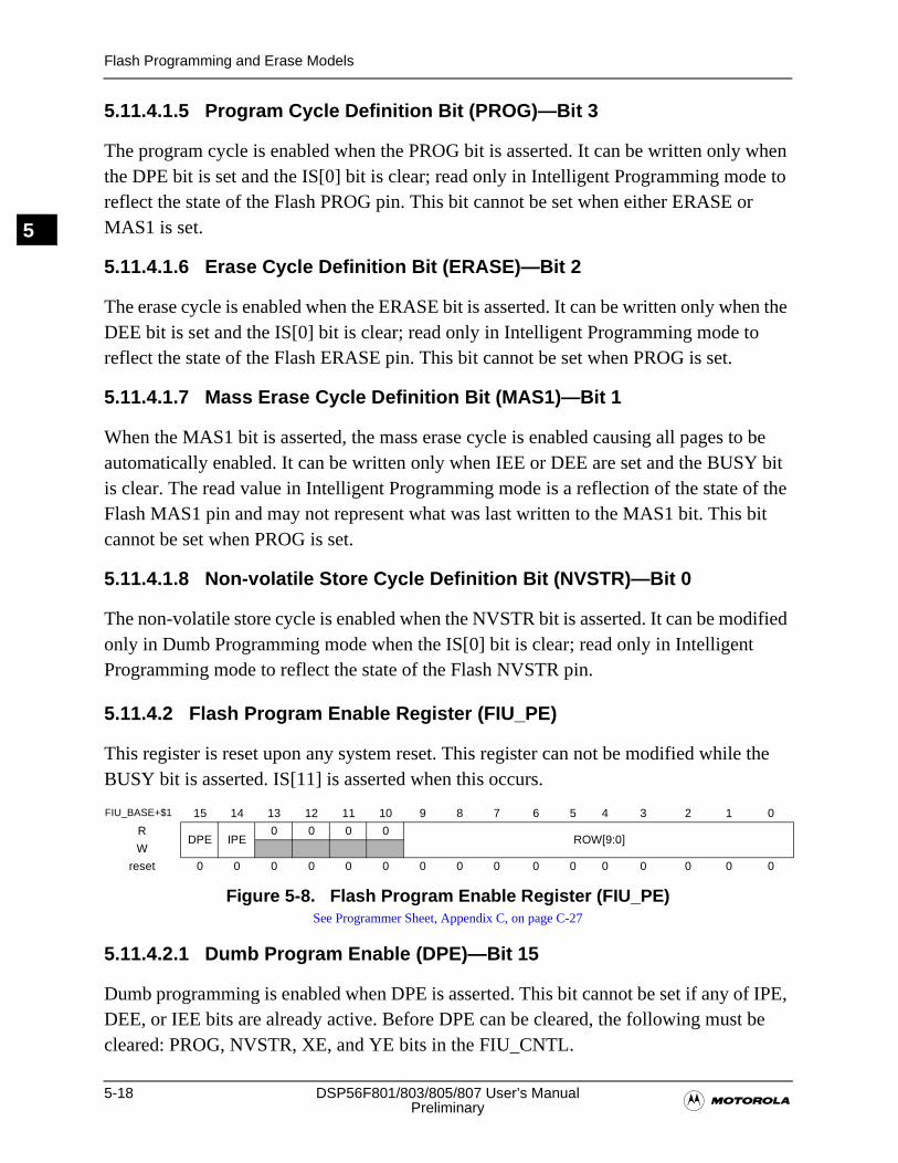
5-18 DSP56F801/803/805/807 User’s Manual�Preliminary
Flash Programming and Erase Models
5
5.11.4.1.5 Program Cycle Definition Bit (PROG)—Bit 3
The program cycle is enabled when the PROG bit is asserted. It can be written only when the DPE bit is set and the IS[0] bit is clear; read only in Intelligent Programming mode to reflect the state of the Flash PROG pin. This bit cannot be set when either ERASE or MAS1 is set.
5.11.4.1.6 Erase Cycle Definition Bit (ERASE)—Bit 2
The erase cycle is enabled when the ERASE bit is asserted. It can be written only when the DEE bit is set and the IS[0] bit is clear; read only in Intelligent Programming mode to reflect the state of the Flash ERASE pin. This bit cannot be set when PROG is set.
5.11.4.1.7 Mass Erase Cycle Definition Bit (MAS1)—Bit 1
When the MAS1 bit is asserted, the mass erase cycle is enabled causing all pages to be automatically enabled. It can be written only when IEE or DEE are set and the BUSY bit is clear. The read value in Intelligent Programming mode is a reflection of the state of the Flash MAS1 pin and may not represent what was last written to the MAS1 bit. This bit cannot be set when PROG is set.
5.11.4.1.8 Non-volatile Store Cycle Definition Bit (NVSTR)—Bit 0
The non-volatile store cycle is enabled when the NVSTR bit is asserted. It can be modified only in Dumb Programming mode when the IS[0] bit is clear; read only in Intelligent Programming mode to reflect the state of the Flash NVSTR pin.
5.11.4.2 Flash Program Enable Register (FIU_PE)
This register is reset upon any system reset. This register can not be modified while the BUSY bit is asserted. IS[11] is asserted when this occurs.
5.11.4.2.1 Dumb Program Enable (DPE)—Bit 15
Dumb programming is enabled when DPE is asserted. This bit cannot be set if any of IPE, DEE, or IEE bits are already active. Before DPE can be cleared, the following must be cleared: PROG, NVSTR, XE, and YE bits in the FIU_CNTL.
FIU_BASE+$1 15 14 13 12 11 10 9 8 7 6 5 4 3 2 1 0
RDPE IPE
0 0 0 0ROW[9:0]
W
reset 0 0 0 0 0 0 0 0 0 0 0 0 0 0 0 0
Figure 5-8. Flash Program Enable Register (FIU_PE)See Programmer Sheet, Appendix C, on page C-27
Flash Programming and Erase Models
�Flash Memory Interface 5-19
Preliminary
5
5.11.4.2.2 Intelligent Program Enable (IPE)—Bit 14
Intelligent programming is enabled when IPE is asserted. This bit cannot be set if any of DPE, DEE, or IEE bits are already active.
5.11.4.2.3 Reserved Bits—Bits 13–10
These reserved bits cannot be modified. They are read as zero.
5.11.4.2.4 Row Number (ROW[9:0])—Bits 9–0
ROW represents the number of the row to be programmed. The ROW number is calculated by forcing the MSB of the target address to zero and right shifting the result five places.
In order to program a row, the row number must be written as ROW[9:0] and the user must perform a write to the same row to begin the programming sequence. Writing to a different row will not start the state machine, nor enable PROG and NVSTR. Interrupt source bit IS[0] is set to indicate an error. This is intended as a double check against accidental programming.
These checks also apply for the Dumb Programming mode.
5.11.4.3 Flash Erase Enable Register (FIU_EE)
This register is reset upon any system reset. This register may not be written while the BUSY bit is asserted. Should this happen, IS[11] is asserted.
5.11.4.3.1 Dumb Erase Enable (DEE)—Bit15
Dumb erase is enabled when the DEE bit is asserted. This bit cannot be set if any of DPE, IPE, or IEE bits are already active. ERASE, NVSTR, XE, and YE must be cleared first before DEE can be cleared.
5.11.4.3.2 Intelligent Erase Enable (IEE)—Bit 14
Intelligent erase is enabled when the IEE bit is asserted. This bit cannot be set if any of DPE, IPE, or DEE bits are already active.
FIU_BASE+$2 15 14 13 12 11 10 9 8 7 6 5 4 3 2 1 0
RDEE IEE
0 0 0 0 0 0 0PAGE[6:0]
W
reset 0 0 0 0 0 0 0 0 0 0 0 0 0 0 0 0
Figure 5-9. Flash Erase Enable Register (FIU_EE)See Programmer Sheet, Appendix C, on page C-27
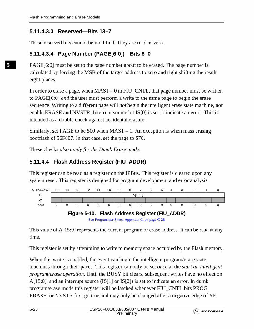
5-20 DSP56F801/803/805/807 User’s Manual�Preliminary
Flash Programming and Erase Models
5
5.11.4.3.3 Reserved—Bits 13–7
These reserved bits cannot be modified. They are read as zero.
5.11.4.3.4 Page Number (PAGE[6:0])—Bits 6–0
PAGE[6:0] must be set to the page number about to be erased. The page number is calculated by forcing the MSB of the target address to zero and right shifting the result eight places.
In order to erase a page, when MAS1 = 0 in FIU_CNTL, that page number must be written to PAGE[6:0] and the user must perform a write to the same page to begin the erase sequence. Writing to a different page will not begin the intelligent erase state machine, nor enable ERASE and NVSTR. Interrupt source bit IS[0] is set to indicate an error. This is intended as a double check against accidental erasure.
Similarly, set PAGE to be $00 when MAS1 = 1. An exception is when mass erasing bootflash of 56F807. In that case, set the page to $78.
These checks also apply for the Dumb Erase mode.
5.11.4.4 Flash Address Register (FIU_ADDR)
This register can be read as a register on the IPBus. This register is cleared upon any system reset. This register is designed for program development and error analysis.
This value of A[15:0] represents the current program or erase address. It can be read at any time.
This register is set by attempting to write to memory space occupied by the Flash memory.
When this write is enabled, the event can begin the intelligent program/erase state machines through their paces. This register can only be set once at the start an intelligent program/erase operation. Until the BUSY bit clears, subsequent writes have no effect on A[15:0], and an interrupt source (IS[1] or IS[2]) is set to indicate an error. In dumb program/erase mode this register will be latched whenever FIU_CNTL bits PROG, ERASE, or NVSTR first go true and may only be changed after a negative edge of YE.
FIU_BASE+$3 15 14 13 12 11 10 9 8 7 6 5 4 3 2 1 0
R A[15:0]
W
reset 0 0 0 0 0 0 0 0 0 0 0 0 0 0 0 0
Figure 5-10. Flash Address Register (FIU_ADDR)See Programmer Sheet, Appendix C, on page C-28
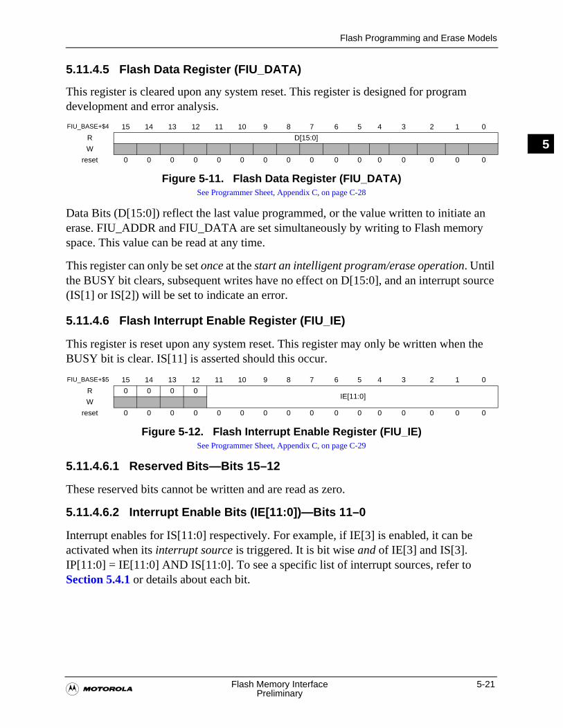
Flash Programming and Erase Models
�Flash Memory Interface 5-21
Preliminary
5
5.11.4.5 Flash Data Register (FIU_DATA)
This register is cleared upon any system reset. This register is designed for program development and error analysis.
Data Bits (D[15:0]) reflect the last value programmed, or the value written to initiate an erase. FIU_ADDR and FIU_DATA are set simultaneously by writing to Flash memory space. This value can be read at any time.
This register can only be set once at the start an intelligent program/erase operation. Until the BUSY bit clears, subsequent writes have no effect on D[15:0], and an interrupt source (IS[1] or IS[2]) will be set to indicate an error.
5.11.4.6 Flash Interrupt Enable Register (FIU_IE)
This register is reset upon any system reset. This register may only be written when the BUSY bit is clear. IS[11] is asserted should this occur.
5.11.4.6.1 Reserved Bits—Bits 15–12
These reserved bits cannot be written and are read as zero.
5.11.4.6.2 Interrupt Enable Bits (IE[11:0])—Bits 11–0
Interrupt enables for IS[11:0] respectively. For example, if IE[3] is enabled, it can be activated when its interrupt source is triggered. It is bit wise and of IE[3] and IS[3]. IP[11:0] = IE[11:0] AND IS[11:0]. To see a specific list of interrupt sources, refer to Section 5.4.1 or details about each bit.
FIU_BASE+$4 15 14 13 12 11 10 9 8 7 6 5 4 3 2 1 0
R D[15:0]
W
reset 0 0 0 0 0 0 0 0 0 0 0 0 0 0 0 0
Figure 5-11. Flash Data Register (FIU_DATA)See Programmer Sheet, Appendix C, on page C-28
FIU_BASE+$5 15 14 13 12 11 10 9 8 7 6 5 4 3 2 1 0
R 0 0 0 0IE[11:0]
W
reset 0 0 0 0 0 0 0 0 0 0 0 0 0 0 0 0
Figure 5-12. Flash Interrupt Enable Register (FIU_IE)See Programmer Sheet, Appendix C, on page C-29
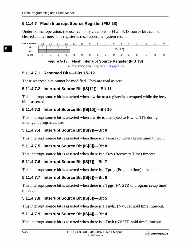
5-22 DSP56F801/803/805/807 User’s Manual�Preliminary
Flash Programming and Erase Models
5
5.11.4.7 Flash Interrupt Source Register (FIU_IS)
Under normal operation, the user can only clear bits in FIU_IS. IS source bits can be cleared at any time. This register is reset upon any system reset.
5.11.4.7.1 Reserved Bits—Bits 15–12
These reserved bits cannot be modified. They are read as zero.
5.11.4.7.2 Interrupt Source Bit (IS[11])—Bit 11
This interrupt source bit is asserted when a write to a register is attempted while the busy bit is asserted.
5.11.4.7.3 Interrupt Source Bit (IS[10])—Bit 10
This interrupt source bit is asserted when a write is attempted to FIU_CNTL during intelligent program/erase.
5.11.4.7.4 Interrupt Source Bit (IS[9])—Bit 9
This interrupt source bit is asserted when there is a Terase or Tmel (Erase time) timeout.
5.11.4.7.5 Interrupt Source Bit (IS[8])—Bit 8
This interrupt source bit is asserted when there is a Trcv (Recovery Time) timeout.
5.11.4.7.6 Interrupt Source Bit (IS[7])—Bit 7
This interrupt source bit is asserted when there is a Tprog (Program time) timeout.
5.11.4.7.7 Interrupt Source Bit (IS[6])—Bit 6
This interrupt source bit is asserted when there is a Tpgs (NVSTR to program setup time) timeout.
5.11.4.7.8 Interrupt Source Bit (IS[5])—Bit 5
This interrupt source bit is asserted when there is a Tnvh1 (NVSTR hold time) timeout.
5.11.4.7.9 Interrupt Source Bit (IS[4])—Bit 4
This interrupt source bit is asserted when there is a Tnvh (NVSTR hold time) timeout.
FIU_BASE+$6 15 14 13 12 11 10 9 8 7 6 5 4 3 2 1 0
R 0 0 0 0IS[11:0]
W
reset 0 0 0 0 0 0 0 0 0 0 0 0 0 0 0 0
Figure 5-13. Flash Interrupt Source Register (FIU_IS)See Programmer Sheet, Appendix C, on page C-30
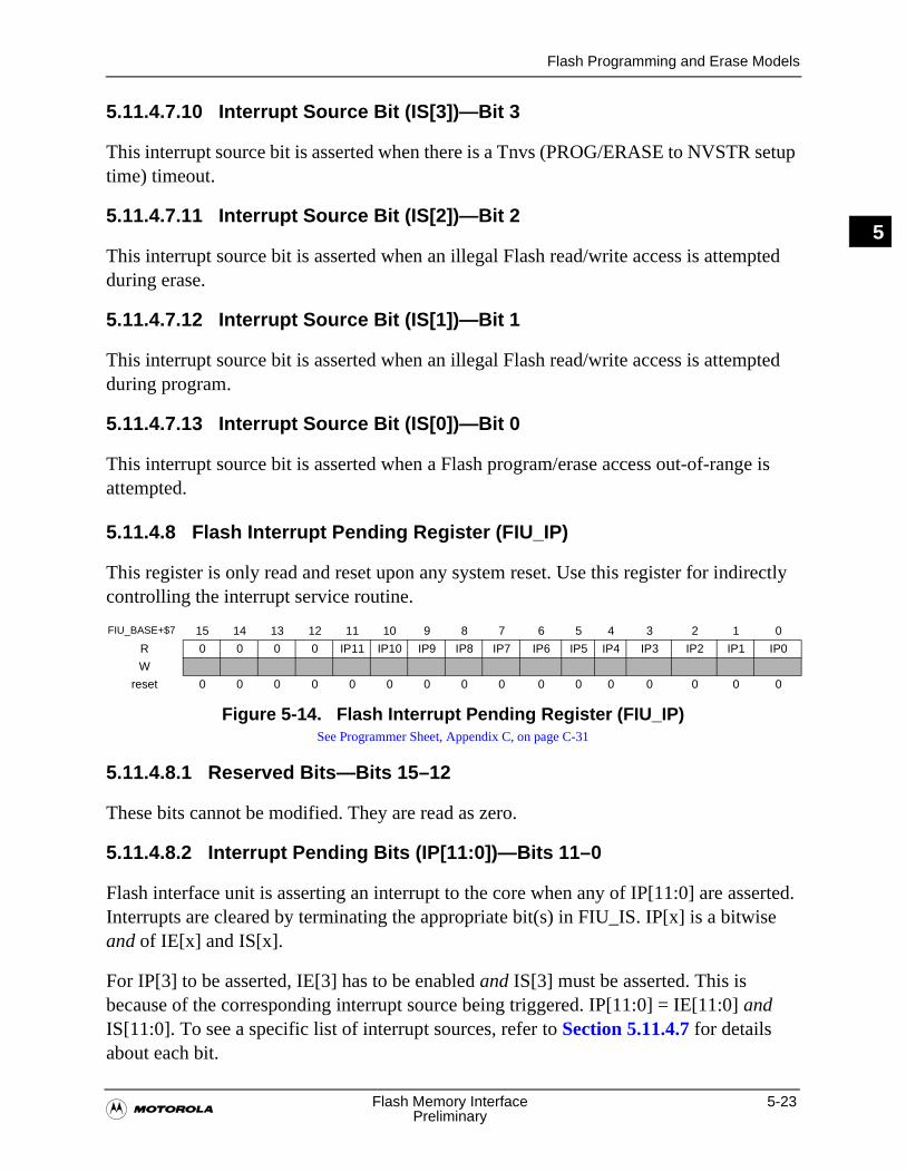
Flash Programming and Erase Models
�Flash Memory Interface 5-23
Preliminary
5
5.11.4.7.10 Interrupt Source Bit (IS[3])—Bit 3
This interrupt source bit is asserted when there is a Tnvs (PROG/ERASE to NVSTR setup time) timeout.
5.11.4.7.11 Interrupt Source Bit (IS[2])—Bit 2
This interrupt source bit is asserted when an illegal Flash read/write access is attempted during erase.
5.11.4.7.12 Interrupt Source Bit (IS[1])—Bit 1
This interrupt source bit is asserted when an illegal Flash read/write access is attempted during program.
5.11.4.7.13 Interrupt Source Bit (IS[0])—Bit 0
This interrupt source bit is asserted when a Flash program/erase access out-of-range is attempted.
5.11.4.8 Flash Interrupt Pending Register (FIU_IP)
This register is only read and reset upon any system reset. Use this register for indirectly controlling the interrupt service routine.
5.11.4.8.1 Reserved Bits—Bits 15–12
These bits cannot be modified. They are read as zero.
5.11.4.8.2 Interrupt Pending Bits (IP[11:0])—Bits 11–0
Flash interface unit is asserting an interrupt to the core when any of IP[11:0] are asserted. Interrupts are cleared by terminating the appropriate bit(s) in FIU_IS. IP[x] is a bitwise and of IE[x] and IS[x].
For IP[3] to be asserted, IE[3] has to be enabled and IS[3] must be asserted. This is because of the corresponding interrupt source being triggered. IP[11:0] = IE[11:0] and IS[11:0]. To see a specific list of interrupt sources, refer to Section 5.11.4.7 for details about each bit.
FIU_BASE+$7 15 14 13 12 11 10 9 8 7 6 5 4 3 2 1 0
R 0 0 0 0 IP11 IP10 IP9 IP8 IP7 IP6 IP5 IP4 IP3 IP2 IP1 IP0
W
reset 0 0 0 0 0 0 0 0 0 0 0 0 0 0 0 0
Figure 5-14. Flash Interrupt Pending Register (FIU_IP)See Programmer Sheet, Appendix C, on page C-31
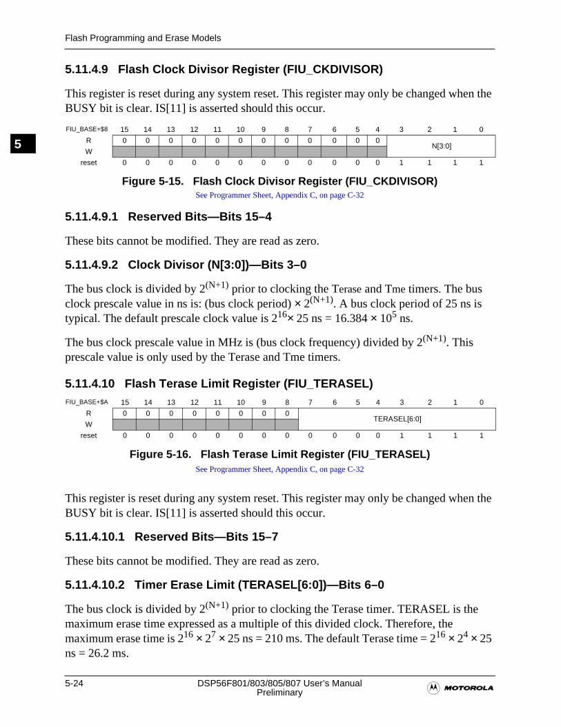
5-24 DSP56F801/803/805/807 User’s Manual�Preliminary
Flash Programming and Erase Models
5
5.11.4.9 Flash Clock Divisor Register (FIU_CKDIVISOR)
This register is reset during any system reset. This register may only be changed when the BUSY bit is clear. IS[11] is asserted should this occur.
5.11.4.9.1 Reserved Bits—Bits 15–4
These bits cannot be modified. They are read as zero.
5.11.4.9.2 Clock Divisor (N[3:0])—Bits 3–0
The bus clock is divided by 2(N+1) prior to clocking the Terase and Tme timers. The bus clock prescale value in ns is: (bus clock period) × 2(N+1). A bus clock period of 25 ns is typical. The default prescale clock value is 216× 25 ns = 16.384 × 10⁵ ns.
The bus clock prescale value in MHz is (bus clock frequency) divided by 2(N+1). This prescale value is only used by the Terase and Tme timers.
5.11.4.10 Flash Terase Limit Register (FIU_TERASEL)
Figure 5-16. Flash Terase Limit Register (FIU_TERASEL)See Programmer Sheet, Appendix C, on page C-32
This register is reset during any system reset. This register may only be changed when the BUSY bit is clear. IS[11] is asserted should this occur.
5.11.4.10.1 Reserved Bits—Bits 15–7
These bits cannot be modified. They are read as zero.
5.11.4.10.2 Timer Erase Limit (TERASEL[6:0])—Bits 6–0
The bus clock is divided by 2(N+1) prior to clocking the Terase timer. TERASEL is the maximum erase time expressed as a multiple of this divided clock. Therefore, the maximum erase time is 216 × 27 × 25 ns = 210 ms. The default Terase time = 216 × 24 × 25 ns = 26.2 ms.
FIU_BASE+$8 15 14 13 12 11 10 9 8 7 6 5 4 3 2 1 0
R 0 0 0 0 0 0 0 0 0 0 0 0N[3:0]
W
reset 0 0 0 0 0 0 0 0 0 0 0 0 1 1 1 1
Figure 5-15. Flash Clock Divisor Register (FIU_CKDIVISOR)See Programmer Sheet, Appendix C, on page C-32
FIU_BASE+$A 15 14 13 12 11 10 9 8 7 6 5 4 3 2 1 0
R 0 0 0 0 0 0 0 0TERASEL[6:0]
W
reset 0 0 0 0 0 0 0 0 0 0 0 0 1 1 1 1
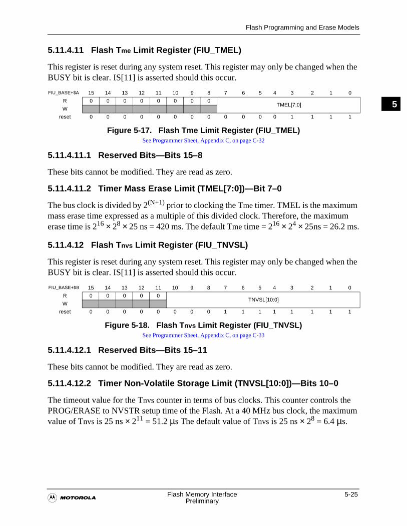
Flash Programming and Erase Models
�Flash Memory Interface 5-25
Preliminary
5
5.11.4.11 Flash Tme Limit Register (FIU_TMEL)
This register is reset during any system reset. This register may only be changed when the BUSY bit is clear. IS[11] is asserted should this occur.
5.11.4.11.1 Reserved Bits—Bits 15–8
These bits cannot be modified. They are read as zero.
5.11.4.11.2 Timer Mass Erase Limit (TMEL[7:0])—Bit 7–0
The bus clock is divided by 2(N+1) prior to clocking the Tme timer. TMEL is the maximum mass erase time expressed as a multiple of this divided clock. Therefore, the maximum erase time is 216 × 28 × 25 ns = 420 ms. The default Tme time = 216 × 24 × 25ns = 26.2 ms.
5.11.4.12 Flash T nvs Limit Register (FIU_TNVSL)
This register is reset during any system reset. This register may only be changed when the BUSY bit is clear. IS[11] is asserted should this occur.
5.11.4.12.1 Reserved Bits—Bits 15–11
These bits cannot be modified. They are read as zero.
5.11.4.12.2 Timer Non-Volatile Storage Limit (TNVSL[10:0])—Bits 10–0
The timeout value for the Tnvs counter in terms of bus clocks. This counter controls the PROG/ERASE to NVSTR setup time of the Flash. At a 40 MHz bus clock, the maximum value of Tnvs is 25 ns × 211 = 51.2 µs The default value of Tnvs is 25 ns × 28 = 6.4 µs.
FIU_BASE+$A 15 14 13 12 11 10 9 8 7 6 5 4 3 2 1 0
R 0 0 0 0 0 0 0 0TMEL[7:0]
W
reset 0 0 0 0 0 0 0 0 0 0 0 0 1 1 1 1
Figure 5-17. Flash Tme Limit Register (FIU_TMEL)See Programmer Sheet, Appendix C, on page C-32
FIU_BASE+$B 15 14 13 12 11 10 9 8 7 6 5 4 3 2 1 0
R 0 0 0 0 0TNVSL[10:0]
W
reset 0 0 0 0 0 0 0 0 1 1 1 1 1 1 1 1
Figure 5-18. Flash Tnvs Limit Register (FIU_TNVSL)See Programmer Sheet, Appendix C, on page C-33
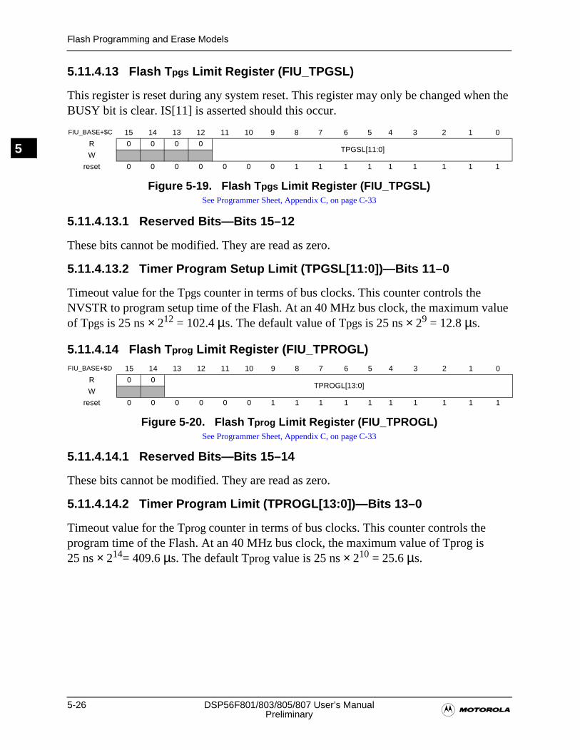
5-26 DSP56F801/803/805/807 User’s Manual�Preliminary
Flash Programming and Erase Models
5
5.11.4.13 Flash Tpgs Limit Register (FIU_TPGSL)
This register is reset during any system reset. This register may only be changed when the BUSY bit is clear. IS[11] is asserted should this occur.
5.11.4.13.1 Reserved Bits—Bits 15–12
These bits cannot be modified. They are read as zero.
5.11.4.13.2 Timer Program Setup Limit (TPGSL[11:0])—Bits 11–0
Timeout value for the Tpgs counter in terms of bus clocks. This counter controls the NVSTR to program setup time of the Flash. At an 40 MHz bus clock, the maximum value of Tpgs is 25 ns × 212 = 102.4 µs. The default value of Tpgs is 25 ns × 29 = 12.8 µs.
5.11.4.14 Flash T prog Limit Register (FIU_TPROGL)
5.11.4.14.1 Reserved Bits—Bits 15–14
These bits cannot be modified. They are read as zero.
5.11.4.14.2 Timer Program Limit (TPROGL[13:0])—Bits 13–0
Timeout value for the Tprog counter in terms of bus clocks. This counter controls the program time of the Flash. At an 40 MHz bus clock, the maximum value of Tprog is 25 ns × 214= 409.6 µs. The default Tprog value is 25 ns × 210 = 25.6 µs.
FIU_BASE+$C 15 14 13 12 11 10 9 8 7 6 5 4 3 2 1 0
R 0 0 0 0TPGSL[11:0]
W
reset 0 0 0 0 0 0 0 1 1 1 1 1 1 1 1 1
Figure 5-19. Flash Tpgs Limit Register (FIU_TPGSL)See Programmer Sheet, Appendix C, on page C-33
FIU_BASE+$D 15 14 13 12 11 10 9 8 7 6 5 4 3 2 1 0
R 0 0TPROGL[13:0]
W
reset 0 0 0 0 0 0 1 1 1 1 1 1 1 1 1 1
Figure 5-20. Flash Tprog Limit Register (FIU_TPROGL)See Programmer Sheet, Appendix C, on page C-33
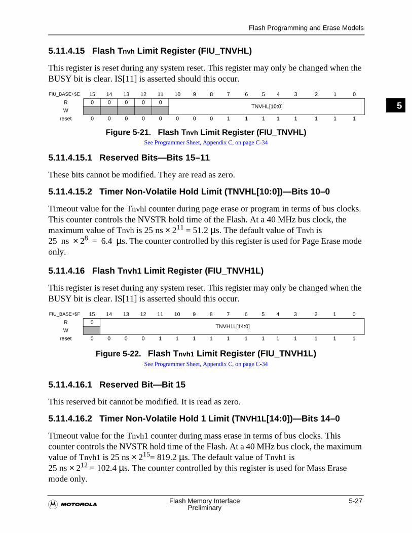
Flash Programming and Erase Models
�Flash Memory Interface 5-27
Preliminary
5
5.11.4.15 Flash Tnvh Limit Register (FIU_TNVHL)
This register is reset during any system reset. This register may only be changed when the BUSY bit is clear. IS[11] is asserted should this occur.
5.11.4.15.1 Reserved Bits—Bits 15–11
These bits cannot be modified. They are read as zero.
5.11.4.15.2 Timer Non-Volatile Hold Limit (TNVHL[10:0])—Bits 10–0
Timeout value for the Tnvhl counter during page erase or program in terms of bus clocks. This counter controls the NVSTR hold time of the Flash. At a 40 MHz bus clock, the maximum value of Tnvh is 25 ns × 211 = 51.2 µs. The default value of Tnvh is 25 ns × 28 = 6.4 µs. The counter controlled by this register is used for Page Erase mode only.
5.11.4.16 Flash T nvh1 Limit Register (FIU_TNVH1L)
This register is reset during any system reset. This register may only be changed when the BUSY bit is clear. IS[11] is asserted should this occur.
Figure 5-22. Flash T nvh1 Limit Register (FIU_TNVH1L)See Programmer Sheet, Appendix C, on page C-34
5.11.4.16.1 Reserved Bit—Bit 15
This reserved bit cannot be modified. It is read as zero.
5.11.4.16.2 Timer Non-Volatile Hold 1 Limit (T NVH1L[14:0])—Bits 14–0
Timeout value for the Tnvh1 counter during mass erase in terms of bus clocks. This counter controls the NVSTR hold time of the Flash. At a 40 MHz bus clock, the maximum value of Tnvh1 is 25 ns × 215= 819.2 µs. The default value of Tnvh1 is 25 ns × 212 = 102.4 µs. The counter controlled by this register is used for Mass Erase mode only.
FIU_BASE+$E 15 14 13 12 11 10 9 8 7 6 5 4 3 2 1 0
R 0 0 0 0 0TNVHL[10:0]
W
reset 0 0 0 0 0 0 0 0 1 1 1 1 1 1 1 1
Figure 5-21. Flash Tnvh Limit Register (FIU_TNVHL)See Programmer Sheet, Appendix C, on page C-34
FIU_BASE+$F 15 14 13 12 11 10 9 8 7 6 5 4 3 2 1 0
R 0TNVH1L[14:0]
W
reset 0 0 0 0 1 1 1 1 1 1 1 1 1 1 1 1
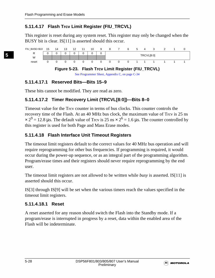
5-28 DSP56F801/803/805/807 User’s Manual�Preliminary
Flash Programming and Erase Models
5
5.11.4.17 Flash Trcv Limit Register (FIU_TRCVL)
This register is reset during any system reset. This register may only be changed when the BUSY bit is clear. IS[11] is asserted should this occur.
5.11.4.17.1 Reserved Bits—Bits 15–9
These bits cannot be modified. They are read as zero.
5.11.4.17.2 Timer Recovery Limit (TRCVL[8:0])—Bits 8–0
Timeout value for the Trcv counter in terms of bus clocks. This counter controls the recovery time of the Flash. At an 40 MHz bus clock, the maximum value of Trcv is 25 ns × 29 = 12.8 µs. The default value of Trcv is 25 ns × 26 = 1.6 µs. The counter controlled by this register is used for both Page and Mass Erase modes.
5.11.4.18 Flash Interface Unit Timeout Registers
The timeout limit registers default to the correct values for 40 MHz bus operation and will require reprogramming for other bus frequencies. If programming is required, it would occur during the power-up sequence, or as an integral part of the programming algorithm. Program/erase times and their registers should never require reprogramming by the end user.
The timeout limit registers are not allowed to be written while busy is asserted. IS[11] is asserted should this occur.
IS[3] through IS[9] will be set when the various timers reach the values specified in the timeout limit registers.
5.11.4.18.1 Reset
A reset asserted for any reason should switch the Flash into the Standby mode. If a program/erase is interrupted in progress by a reset, data within the enabled area of the Flash will be indeterminate.
FIU_BASE+$10 15 14 13 12 11 10 9 8 7 6 5 4 3 2 1 0
R 0 0 0 0 0 0 0TRCVL[8:0]
W
reset 0 0 0 0 0 0 0 0 0 0 1 1 1 1 1 1
Figure 5-23. Flash Trcv Limit Register (FIU_TRCVL)See Programmer Sheet, Appendix C, on page C-34
Flash Programming and Erase Models
�Flash Memory Interface 5-29
Preliminary
5
5.11.4.18.2 BUSY
The busy bit in the FIU_CNTL register will be set if any of the following are true:
• If PROG is asserted
• If NVSTR is asserted
• If ERASE is asserted
If the Trcv counter is running intelligent Program/Erase mode
Flash reads should not be attempted while busy is asserted.
The core should be prevented from entering Sleep or Low-Power mode if busy is asserted OR FIU_IS not equal to $0000.
The busy bit is cleared once PROG, NVSTR, ERASE, XE and YE bits have been cleared.
5.11.4.18.3 Interrupts
The FIU OR’s all bits in the FIU_IP register to determine the value of the single interrupt signal presented to the host processor interrupt controller.
The Interrupt Pending register (FIU_IP) is equal to the bit-wise anding of the Interrupt Enable register (FIU_IE) and the Interrupt Source register (FIU_IS). Interrupt sources may be polled at any time (in the FIU_IS register), even if those sources are disabled. The FIU_IP register reflects only those sources causing an interrupt to the host processor.
• Interrupts must be cleared by clearing the appropriate bit in the FIU_IS register. This is done by the core under software control
• The FIU is responsible for generating read-out-of-range-interrupts when the information block is enabled. But an attempt must also be made to access past the two rows of that particular block, but within the overall size of the main block. The FIU is not responsible for generating interrupts for accesses outside of this range
• If the host processor attempts a read or write to the Flash while it is being erased or programmed, the FIU will generate an interrupt. It will not affect the contents of the limit register in question if the corresponding enable bit in FIU_IE is set
• Writes to the FIU_CNTL register are prohibited once the intelligent program/erase sequences are begun by the FIU state machine. It is not legal to change these settings until after the program/erase task is complete and the BUSY bit is clear. Any attempt to do so will not affect the register contents, and may cause an error interrupt to be posted if the corresponding enable bit in FIU_IE is set

5-30 DSP56F801/803/805/807 User’s Manual�Preliminary
Flash Programming and Erase Models
5
�External Memory Interface 6-1
Preliminary
6
Chapter 6External Memory Interface

6-2 DSP56F801/803/805/807 User’s Manual�Preliminary
6
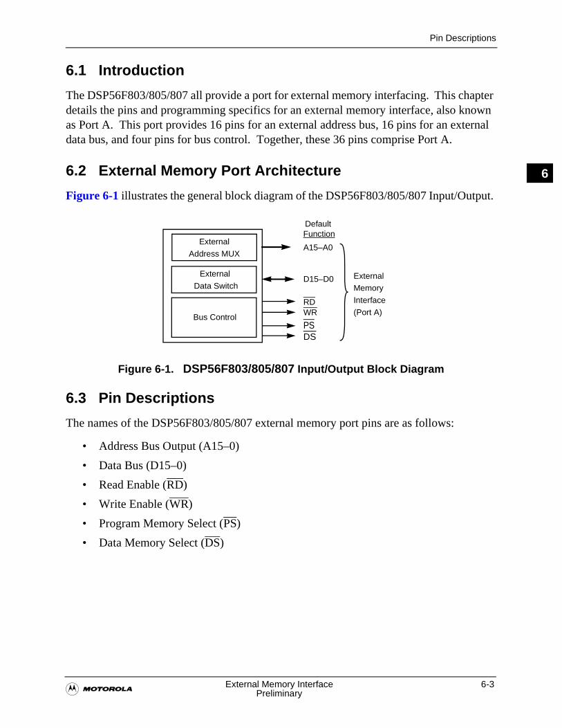
Pin Descriptions
�External Memory Interface 6-3
Preliminary
6
6.1 Introduction
The DSP56F803/805/807 all provide a port for external memory interfacing. This chapter details the pins and programming specifics for an external memory interface, also known as Port A. This port provides 16 pins for an external address bus, 16 pins for an external data bus, and four pins for bus control. Together, these 36 pins comprise Port A.
6.2 External Memory Port Architecture
Figure 6-1 illustrates the general block diagram of the DSP56F803/805/807 Input/Output.
6.3 Pin Descriptions
The names of the DSP56F803/805/807 external memory port pins are as follows:
• Address Bus Output (A15–0)
• Data Bus (D15–0)
• Read Enable (RD)
• Write Enable (WR)
• Program Memory Select (PS)
• Data Memory Select (DS)
Figure 6-1. DSP56F803/805/807 Input/Output Block Diagram
D15–D0
A15–A0External
Address MUX
Bus Control
DS
RDWR
External
Data Switch
DefaultFunction
PS
External
(Port A)
Memory
Interface
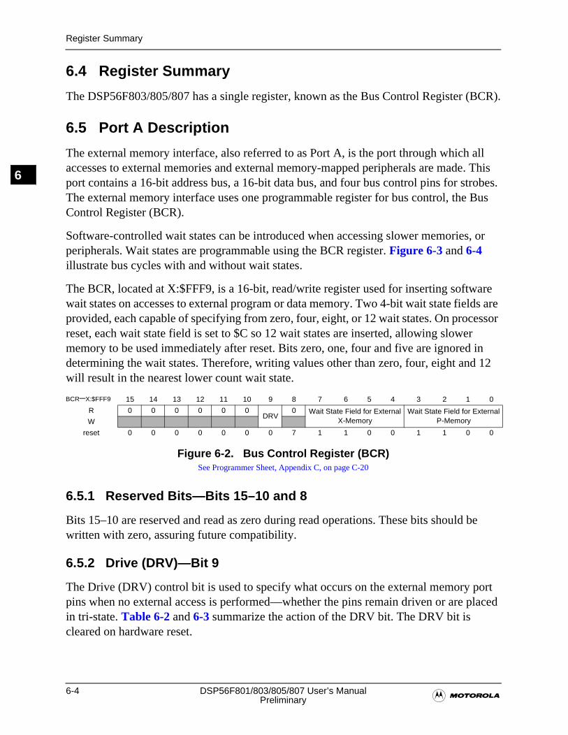
6-4 DSP56F801/803/805/807 User’s Manual�Preliminary
Register Summary
6
6.4 Register Summary
The DSP56F803/805/807 has a single register, known as the Bus Control Register (BCR).
6.5 Port A Description
The external memory interface, also referred to as Port A, is the port through which all accesses to external memories and external memory-mapped peripherals are made. This port contains a 16-bit address bus, a 16-bit data bus, and four bus control pins for strobes. The external memory interface uses one programmable register for bus control, the Bus Control Register (BCR).
Software-controlled wait states can be introduced when accessing slower memories, or peripherals. Wait states are programmable using the BCR register. Figure 6-3 and 6-4 illustrate bus cycles with and without wait states.
The BCR, located at X:$FFF9, is a 16-bit, read/write register used for inserting software wait states on accesses to external program or data memory. Two 4-bit wait state fields are provided, each capable of specifying from zero, four, eight, or 12 wait states. On processor reset, each wait state field is set to $C so 12 wait states are inserted, allowing slower memory to be used immediately after reset. Bits zero, one, four and five are ignored in determining the wait states. Therefore, writing values other than zero, four, eight and 12 will result in the nearest lower count wait state.
Figure 6-2. Bus Control Register (BCR)See Programmer Sheet, Appendix C, on page C-20
6.5.1 Reserved Bits—Bits 15–10 and 8
Bits 15–10 are reserved and read as zero during read operations. These bits should be written with zero, assuring future compatibility.
6.5.2 Drive (DRV)—Bit 9
The Drive (DRV) control bit is used to specify what occurs on the external memory port pins when no external access is performed—whether the pins remain driven or are placed in tri-state. Table 6-2 and 6-3 summarize the action of the DRV bit. The DRV bit is cleared on hardware reset.
BCR–X:$FFF9 15 14 13 12 11 10 9 8 7 6 5 4 3 2 1 0
R 0 0 0 0 0 0DRV
0 Wait State Field for External X-Memory
Wait State Field for External P-MemoryW
reset 0 0 0 0 0 0 0 7 1 1 0 0 1 1 0 0
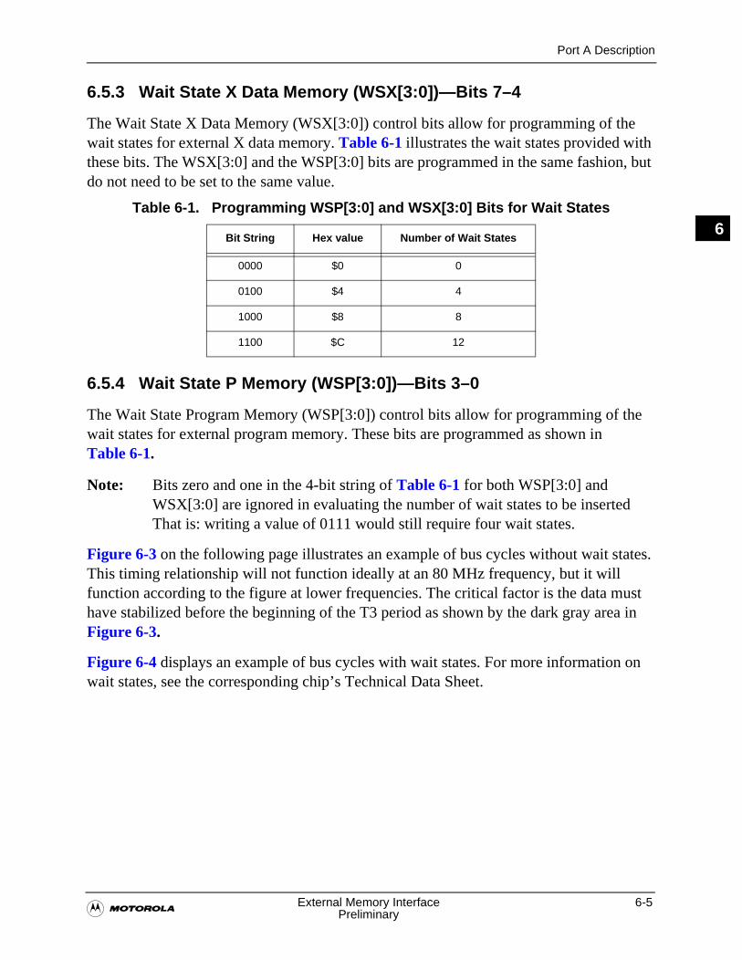
Port A Description
�External Memory Interface 6-5
Preliminary
6
6.5.3 Wait State X Data Memory (WSX[3:0])—Bits 7–4
The Wait State X Data Memory (WSX[3:0]) control bits allow for programming of the wait states for external X data memory. Table 6-1 illustrates the wait states provided with these bits. The WSX[3:0] and the WSP[3:0] bits are programmed in the same fashion, but do not need to be set to the same value.
6.5.4 Wait State P Memory (WSP[3:0])—Bits 3–0
The Wait State Program Memory (WSP[3:0]) control bits allow for programming of the wait states for external program memory. These bits are programmed as shown in Table 6-1.
Note: Bits zero and one in the 4-bit string of Table 6-1 for both WSP[3:0] and WSX[3:0] are ignored in evaluating the number of wait states to be inserted That is: writing a value of 0111 would still require four wait states.
Figure 6-3 on the following page illustrates an example of bus cycles without wait states. This timing relationship will not function ideally at an 80 MHz frequency, but it will function according to the figure at lower frequencies. The critical factor is the data must have stabilized before the beginning of the T3 period as shown by the dark gray area in Figure 6-3.
Figure 6-4 displays an example of bus cycles with wait states. For more information on wait states, see the corresponding chip’s Technical Data Sheet.
Table 6-1. Programming WSP[3:0] and WSX[3:0] Bits for Wait States
Bit String Hex value Number of Wait States
0000 $0 0
0100 $4 4
1000 $8 8
1100 $C 12
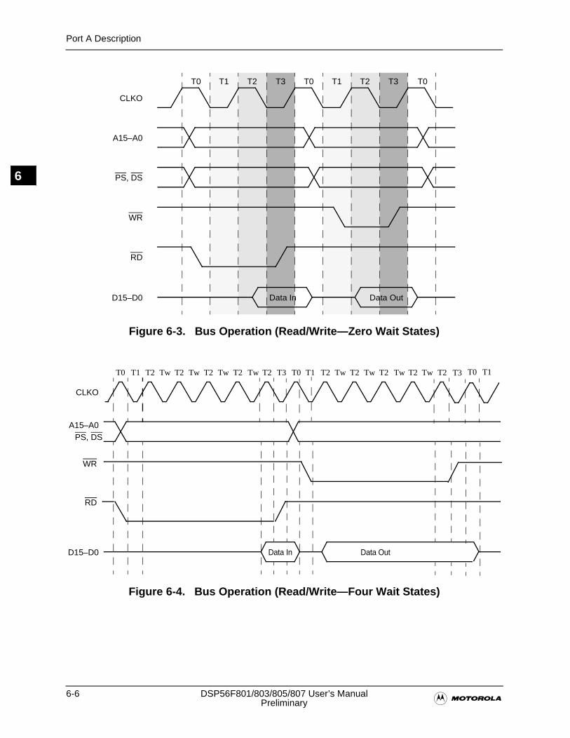
6-6 DSP56F801/803/805/807 User’s Manual�Preliminary
Port A Description
6
Figure 6-3. Bus Operation (Read/Write—Zero Wait States)
Figure 6-4. Bus Operation (Read/Write—Four Wait States)
Data In Data OutD15–D0
RD
WR
A15–A0
PS, DS
CLKO
T0 T1 T2 T3 T0 T1 T2 T3 T0
T0 T1 T2 Tw T2 Tw T2 T3T2 Tw T2 Tw T0 T1 T2 Tw T2 Tw T2 Tw T2 Tw
Data In Data OutD15–D0
WR
A15–A0
CLKO
PS, DS
RD
T2 T3 T0 T1
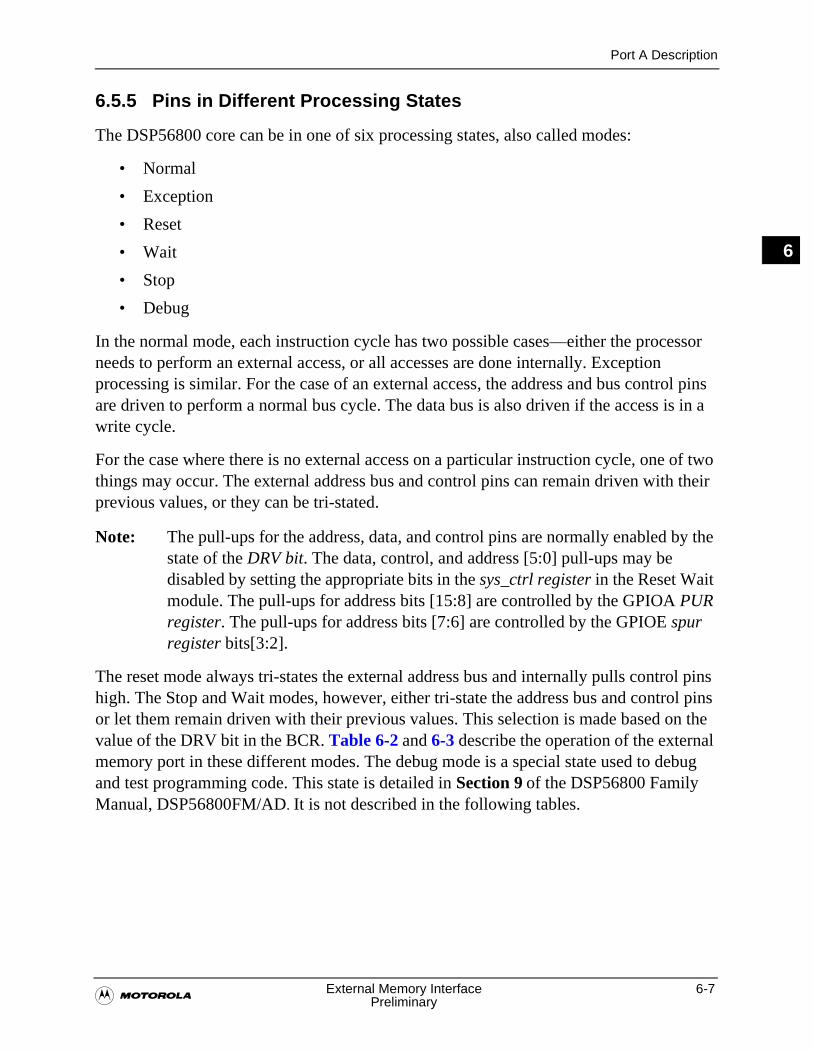
Port A Description
�External Memory Interface 6-7
Preliminary
6
6.5.5 Pins in Different Processing States
The DSP56800 core can be in one of six processing states, also called modes:
• Normal
• Exception
• Reset
• Wait
• Stop
• Debug
In the normal mode, each instruction cycle has two possible cases—either the processor needs to perform an external access, or all accesses are done internally. Exception processing is similar. For the case of an external access, the address and bus control pins are driven to perform a normal bus cycle. The data bus is also driven if the access is in a write cycle.
For the case where there is no external access on a particular instruction cycle, one of two things may occur. The external address bus and control pins can remain driven with their previous values, or they can be tri-stated.
Note: The pull-ups for the address, data, and control pins are normally enabled by the state of the DRV bit. The data, control, and address [5:0] pull-ups may be disabled by setting the appropriate bits in the sys_ctrl register in the Reset Wait module. The pull-ups for address bits [15:8] are controlled by the GPIOA PUR register. The pull-ups for address bits [7:6] are controlled by the GPIOE spur register bits[3:2].
The reset mode always tri-states the external address bus and internally pulls control pins high. The Stop and Wait modes, however, either tri-state the address bus and control pins or let them remain driven with their previous values. This selection is made based on the value of the DRV bit in the BCR. Table 6-2 and 6-3 describe the operation of the external memory port in these different modes. The debug mode is a special state used to debug and test programming code. This state is detailed in Section 9 of the DSP56800 Family Manual, DSP56800FM/AD. It is not described in the following tables.
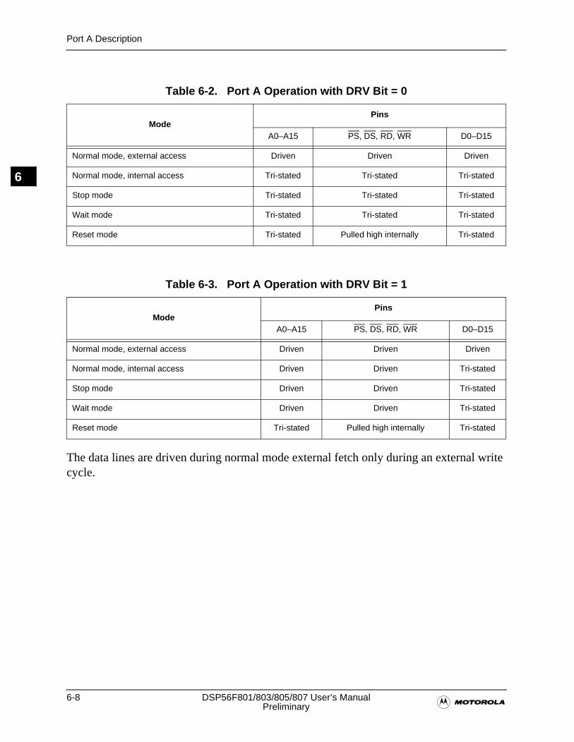
6-8 DSP56F801/803/805/807 User’s Manual�Preliminary
Port A Description
6
The data lines are driven during normal mode external fetch only during an external write cycle.
Table 6-2. Port A Operation with DRV Bit = 0
ModePins
A0–A15 PS, DS, RD, WR D0–D15
Normal mode, external access Driven Driven Driven
Normal mode, internal access Tri-stated Tri-stated Tri-stated
Stop mode Tri-stated Tri-stated Tri-stated
Wait mode Tri-stated Tri-stated Tri-stated
Reset mode Tri-stated Pulled high internally Tri-stated
Table 6-3. Port A Operation with DRV Bit = 1
ModePins
A0–A15 PS, DS, RD, WR D0–D15
Normal mode, external access Driven Driven Driven
Normal mode, internal access Driven Driven Tri-stated
Stop mode Driven Driven Tri-stated
Wait mode Driven Driven Tri-stated
Reset mode Tri-stated Pulled high internally Tri-stated
�General Purpose Input/Output (GPIO) 7-1
Preliminary
7
Chapter 7General Purpose Input/Output (GPIO)

7-2 DSP56F801/803/805/807 User’s Manual�Preliminary
7
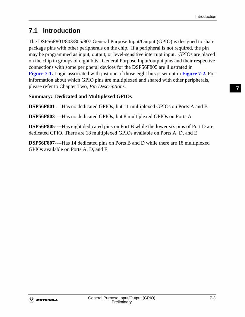
Introduction
�General Purpose Input/Output (GPIO) 7-3
Preliminary
7
7.1 Introduction
The DSP56F801/803/805/807 General Purpose Input/Output (GPIO) is designed to share package pins with other peripherals on the chip. If a peripheral is not required, the pin may be programmed as input, output, or level-sensitive interrupt input. GPIOs are placed on the chip in groups of eight bits. General Purpose Input/output pins and their respective connections with some peripheral devices for the DSP56F805 are illustrated in Figure 7-1. Logic associated with just one of those eight bits is set out in Figure 7-2. For information about which GPIO pins are multiplexed and shared with other peripherals, please refer to Chapter Two, Pin Descriptions.
Summary: Dedicated and Multiplexed GPIOs
DSP56F801----Has no dedicated GPIOs; but 11 multiplexed GPIOs on Ports A and B
DSP56F803----Has no dedicated GPIOs; but 8 multiplexed GPIOs on Ports A
DSP56F805----Has eight dedicated pins on Port B while the lower six pins of Port D are dedicated GPIO. There are 18 multiplexed GPIOs available on Ports A, D, and E
DSP56F807----Has 14 dedicated pins on Ports B and D while there are 18 multiplexed GPIOs available on Ports A, D, and E
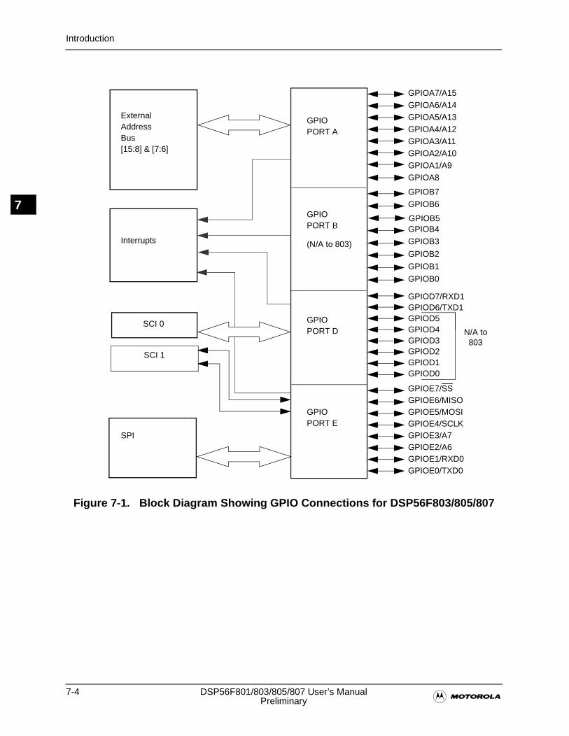
7-4 DSP56F801/803/805/807 User’s Manual�Preliminary
Introduction
7
Figure 7-1. Block Diagram Showing GPIO Connections for DSP56F803/805/807
GPIO
GPIO
GPIO
GPIO
PORT A
PORT B
PORT D
PORT E
GPIOA7/A15GPIOA6/A14GPIOA5/A13GPIOA4/A12
GPIOA3/A11GPIOA2/A10GPIOA1/A9GPIOA8
GPIOB7
GPIOB6
GPIOB4
GPIOB3
GPIOB2
GPIOB1
GPIOB0
GPIOD7/RXD1GPIOD6/TXD1GPIOD5GPIOD4GPIOD3GPIOD2GPIOD1GPIOD0
GPIOE7/SSGPIOE6/MISOGPIOE5/MOSIGPIOE4/SCLKGPIOE3/A7GPIOE2/A6GPIOE1/RXD0GPIOE0/TXD0
ExternalAddressBus
Interrupts
SPI
[15:8] & [7:6]
(N/A to 803)
N/A to 803
SCI 0
SCI 1
GPIOB5
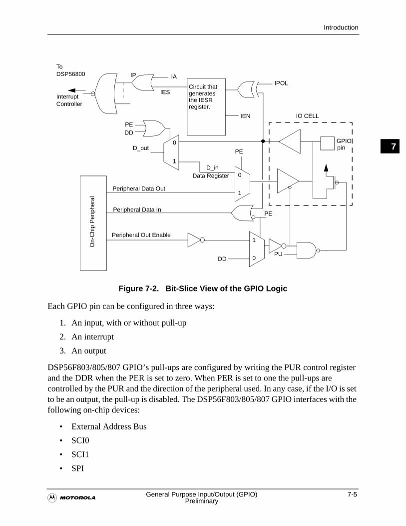
Introduction
�General Purpose Input/Output (GPIO) 7-5
Preliminary
7
Figure 7-2. Bit-Slice View of the GPIO Logic
Each GPIO pin can be configured in three ways:
1. An input, with or without pull-up
2. An interrupt
3. An output
DSP56F803/805/807 GPIO’s pull-ups are configured by writing the PUR control register and the DDR when the PER is set to zero. When PER is set to one the pull-ups are controlled by the PUR and the direction of the peripheral used. In any case, if the I/O is set to be an output, the pull-up is disabled. The DSP56F803/805/807 GPIO interfaces with the following on-chip devices:
• External Address Bus
• SCI0
• SCI1
• SPI
D_in
On-
Chi
p P
erip
hera
l
D_out0
1
Peripheral Data Out
PE
0
1
Peripheral Data InPE
0
1
DDPU
IPTo DSP56800
Interrupt Controller
IES
IA
IEN
IPOLCircuit thatgenerates the IESRregister.
Peripheral Out Enable
IO CELL
Data Register
PEDD
GPIOpin
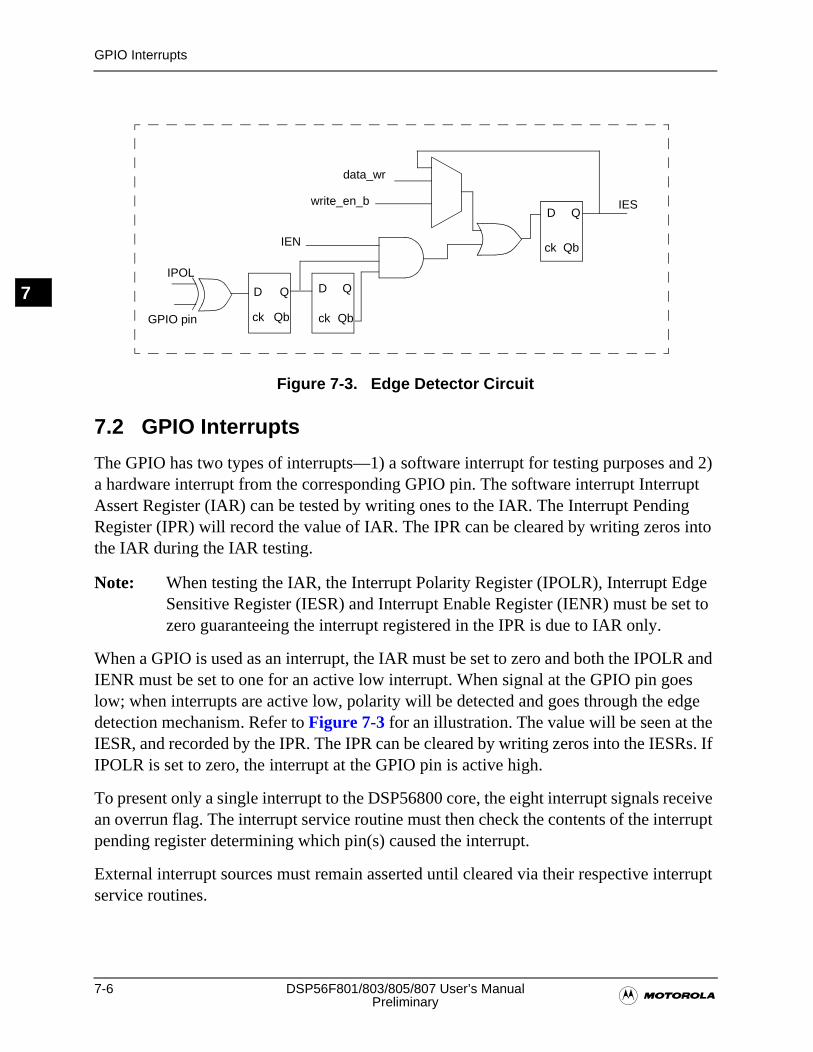
7-6 DSP56F801/803/805/807 User’s Manual�Preliminary
GPIO Interrupts
7
Figure 7-3. Edge Detector Circuit
7.2 GPIO Interrupts
The GPIO has two types of interrupts—1) a software interrupt for testing purposes and 2) a hardware interrupt from the corresponding GPIO pin. The software interrupt Interrupt Assert Register (IAR) can be tested by writing ones to the IAR. The Interrupt Pending Register (IPR) will record the value of IAR. The IPR can be cleared by writing zeros into the IAR during the IAR testing.
Note: When testing the IAR, the Interrupt Polarity Register (IPOLR), Interrupt Edge Sensitive Register (IESR) and Interrupt Enable Register (IENR) must be set to zero guaranteeing the interrupt registered in the IPR is due to IAR only.
When a GPIO is used as an interrupt, the IAR must be set to zero and both the IPOLR and IENR must be set to one for an active low interrupt. When signal at the GPIO pin goes low; when interrupts are active low, polarity will be detected and goes through the edge detection mechanism. Refer to Figure 7-3 for an illustration. The value will be seen at the IESR, and recorded by the IPR. The IPR can be cleared by writing zeros into the IESRs. If IPOLR is set to zero, the interrupt at the GPIO pin is active high.
To present only a single interrupt to the DSP56800 core, the eight interrupt signals receive an overrun flag. The interrupt service routine must then check the contents of the interrupt pending register determining which pin(s) caused the interrupt.
External interrupt sources must remain asserted until cleared via their respective interrupt service routines.
D Q
ck Qb
D
ck
Q
Qb
D Q
ck Qb
IPOL
GPIO pin
data_wr
write_en_b
IEN
IES
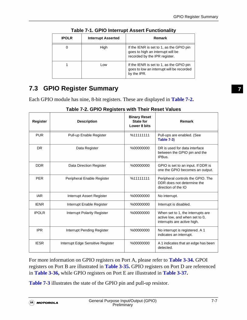
GPIO Register Summary
�General Purpose Input/Output (GPIO) 7-7
Preliminary
7
Table 7-1. GPIO Interrupt Assert Functionality
7.3 GPIO Register Summary
Each GPIO module has nine, 8-bit registers. These are displayed in Table 7-2.
Table 7-2. GPIO Registers with Their Reset Values
For more information on GPIO registers on Port A, please refer to Table 3-34. GPOI registers on Port B are illustrated in Table 3-35. GPIO registers on Port D are referenced in Table 3-36, while GPIO registers on Port E are illustrated in Table 3-37.
Table 7-3 illustrates the state of the GPIO pin and pull-up resistor.
IPOLR Interrupt Asserted Remark
0 High If the IENR is set to 1, as the GPIO pin goes to high an interrupt will be recorded by the IPR register.
1 Low If the IENR is set to 1, as the GPIO pin goes to low an interrupt will be recorded by the IPR.
Register DescriptionBinary Reset
State for Lower 8 bits
Remark
PUR Pull-up Enable Register %11111111 Pull-ups are enabled. (See Table 7-3)
DR Data Register %00000000 DR is used for data interface between the GPIO pin and the IPBus.
DDR Data Direction Register %00000000 GPIO is set to an input. If DDR is one the GPIO becomes an output.
PER Peripheral Enable Register %11111111 Peripheral controls the GPIO. The DDR does not determine the direction of the IO
IAR Interrupt Assert Register %00000000 No interrupt.
IENR Interrupt Enable Register %00000000 Interrupt is disabled.
IPOLR Interrupt Polarity Register %00000000 When set to 1, the interrupts are active low, and when set to 0, interrupts are active high.
IPR Interrupt Pending Register %00000000 No interrupt is registered. A 1 indicates an interrupt.
IESR Interrupt Edge Sensitive Register %00000000 A 1 indicates that an edge has been detected.
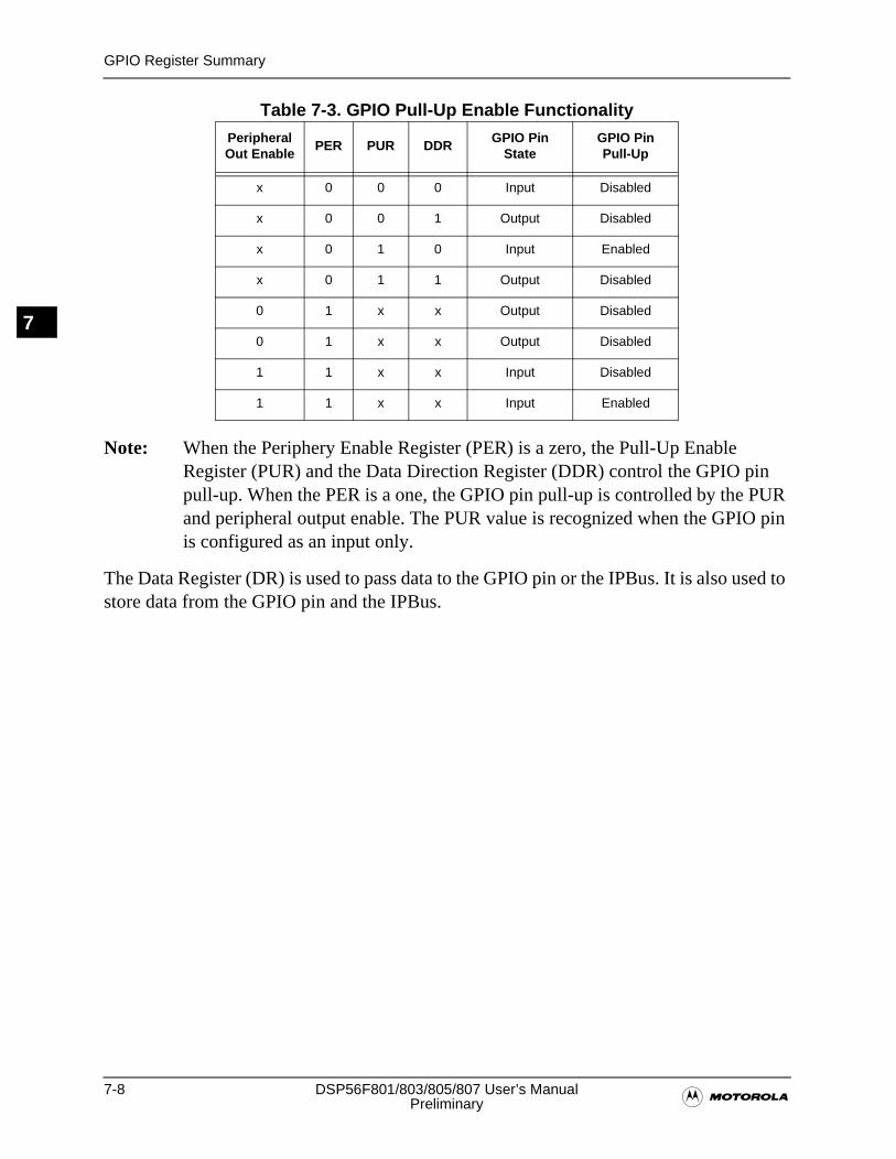
7-8 DSP56F801/803/805/807 User’s Manual�Preliminary
GPIO Register Summary
7
Table 7-3. GPIO Pull-Up Enable Functionality
Note: When the Periphery Enable Register (PER) is a zero, the Pull-Up Enable Register (PUR) and the Data Direction Register (DDR) control the GPIO pin pull-up. When the PER is a one, the GPIO pin pull-up is controlled by the PUR and peripheral output enable. The PUR value is recognized when the GPIO pin is configured as an input only.
The Data Register (DR) is used to pass data to the GPIO pin or the IPBus. It is also used to store data from the GPIO pin and the IPBus.
Peripheral Out Enable
PER PUR DDRGPIO Pin
StateGPIO Pin Pull-Up
x 0 0 0 Input Disabled
x 0 0 1 Output Disabled
x 0 1 0 Input Enabled
x 0 1 1 Output Disabled
0 1 x x Output Disabled
0 1 x x Output Disabled
1 1 x x Input Disabled
1 1 x x Input Enabled
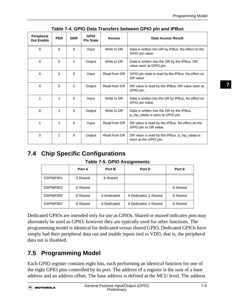
Programming Model
�General Purpose Input/Output (GPIO) 7-9
Preliminary
7
Table 7-4. GPIO Data Transfers between GPIO pin and IPBus
7.4 Chip Specific ConfigurationsTable 7-5. GPIO Assignments
Dedicated GPIOs are intended only for use as GPIOs. Shared or muxed indicates pins may alternately be used as GPIO; however they are typically used for other functions. The programming model is identical for dedicated versus shared GPIO. Dedicated GPIOs have simply had their peripheral data out and enable inputs tied to VDD, that is, the peripheral data out is disabled.
7.5 Programming Model
Each GPIO register contains eight bits, each performing an identical function for one of the eight GPIO pins controlled by its port. The address of a register is the sum of a base address and an address offset. The base address is defined at the MCU level. The address
Peripheral Out Enable
PER DDRGPIO
Pin StateAccess Data Access Result
X 0 0 Input Write to DR Data is written into DR by IPBus. No effect on the GPIO pin value.
X 0 1 Output Write to DR Data is written into the DR by the IPBus. DR value seen at GPIO pin.
X 0 0 Input Read from DR GPIO pin state is read by the IPBus. No effect on DR value.
X 0 1 Output Read from DR DR value is read by the IPBus. DR value seen at GPIO pin.
1 1 X Input Write to DR Data is written into the DR by IPBus. No effect on GPIO pin value.
0 1 X Output Write to DR Data is written into the DR by the IPBus. p_mp_odata is seen at GPIO pin.
1 1 X Input Read from DR DR value is read by the IPBus. No effect on the GPIO pin or DR value.
0 1 X Output Read from DR DR value is read by the IPBus. p_mp_odata is seen at the GPIO pin.
Port A Port B Port D Port E
DSP56F801 3 Shared 8 Shared
DSP56F803 8 Shared 8 Shared
DSP56F805 8 Shared 8 Dedicated 6 Dedicated, 2 Shared 8 Shared
DSP56F807 8 Shared 8 Dedicated 6 Dedicated, 2 Shared 8 Shared
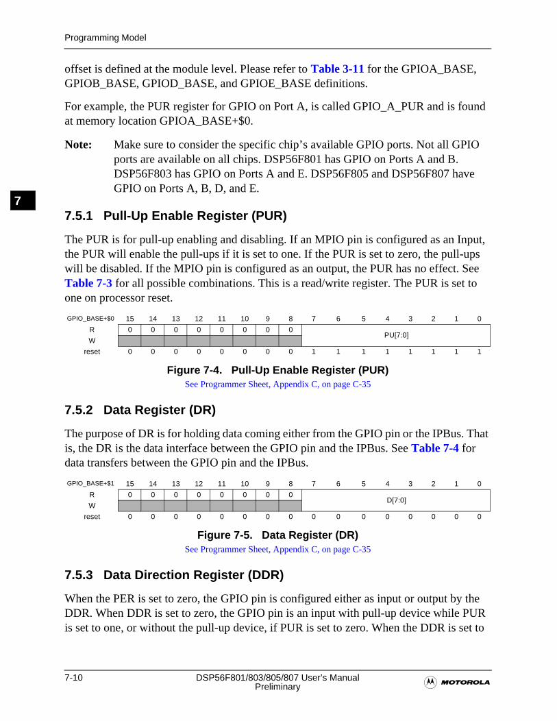
7-10 DSP56F801/803/805/807 User’s Manual�Preliminary
Programming Model
7
offset is defined at the module level. Please refer to Table 3-11 for the GPIOA_BASE, GPIOB_BASE, GPIOD_BASE, and GPIOE_BASE definitions.
For example, the PUR register for GPIO on Port A, is called GPIO_A_PUR and is found at memory location GPIOA_BASE+$0.
Note: Make sure to consider the specific chip’s available GPIO ports. Not all GPIO ports are available on all chips. DSP56F801 has GPIO on Ports A and B. DSP56F803 has GPIO on Ports A and E. DSP56F805 and DSP56F807 have GPIO on Ports A, B, D, and E.
7.5.1 Pull-Up Enable Register (PUR)
The PUR is for pull-up enabling and disabling. If an MPIO pin is configured as an Input, the PUR will enable the pull-ups if it is set to one. If the PUR is set to zero, the pull-ups will be disabled. If the MPIO pin is configured as an output, the PUR has no effect. See Table 7-3 for all possible combinations. This is a read/write register. The PUR is set to one on processor reset.
7.5.2 Data Register (DR)
The purpose of DR is for holding data coming either from the GPIO pin or the IPBus. That is, the DR is the data interface between the GPIO pin and the IPBus. See Table 7-4 for data transfers between the GPIO pin and the IPBus.
7.5.3 Data Direction Register (DDR)
When the PER is set to zero, the GPIO pin is configured either as input or output by the DDR. When DDR is set to zero, the GPIO pin is an input with pull-up device while PUR is set to one, or without the pull-up device, if PUR is set to zero. When the DDR is set to
GPIO_BASE+$0 15 14 13 12 11 10 9 8 7 6 5 4 3 2 1 0
R 0 0 0 0 0 0 0 0PU[7:0]
W
reset 0 0 0 0 0 0 0 0 1 1 1 1 1 1 1 1
Figure 7-4. Pull-Up Enable Register (PUR)See Programmer Sheet, Appendix C, on page C-35
GPIO_BASE+$1 15 14 13 12 11 10 9 8 7 6 5 4 3 2 1 0
R 0 0 0 0 0 0 0 0D[7:0]
W
reset 0 0 0 0 0 0 0 0 0 0 0 0 0 0 0 0
Figure 7-5. Data Register (DR)See Programmer Sheet, Appendix C, on page C-35
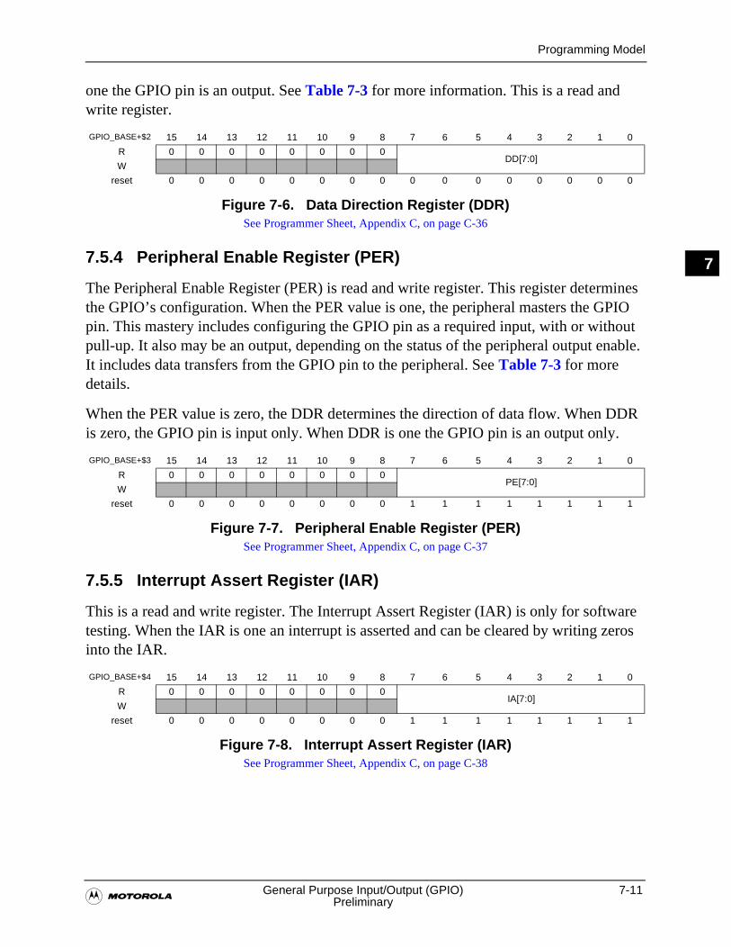
Programming Model
�General Purpose Input/Output (GPIO) 7-11
Preliminary
7
one the GPIO pin is an output. See Table 7-3 for more information. This is a read and write register.
7.5.4 Peripheral Enable Register (PER)
The Peripheral Enable Register (PER) is read and write register. This register determines the GPIO’s configuration. When the PER value is one, the peripheral masters the GPIO pin. This mastery includes configuring the GPIO pin as a required input, with or without pull-up. It also may be an output, depending on the status of the peripheral output enable. It includes data transfers from the GPIO pin to the peripheral. See Table 7-3 for more details.
When the PER value is zero, the DDR determines the direction of data flow. When DDR is zero, the GPIO pin is input only. When DDR is one the GPIO pin is an output only.
7.5.5 Interrupt Assert Register (IAR)
This is a read and write register. The Interrupt Assert Register (IAR) is only for software testing. When the IAR is one an interrupt is asserted and can be cleared by writing zeros into the IAR.
GPIO_BASE+$2 15 14 13 12 11 10 9 8 7 6 5 4 3 2 1 0
R 0 0 0 0 0 0 0 0DD[7:0]
W
reset 0 0 0 0 0 0 0 0 0 0 0 0 0 0 0 0
Figure 7-6. Data Direction Register (DDR)See Programmer Sheet, Appendix C, on page C-36
GPIO_BASE+$3 15 14 13 12 11 10 9 8 7 6 5 4 3 2 1 0
R 0 0 0 0 0 0 0 0PE[7:0]
W
reset 0 0 0 0 0 0 0 0 1 1 1 1 1 1 1 1
Figure 7-7. Peripheral Enable Register (PER)See Programmer Sheet, Appendix C, on page C-37
GPIO_BASE+$4 15 14 13 12 11 10 9 8 7 6 5 4 3 2 1 0
R 0 0 0 0 0 0 0 0IA[7:0]
W
reset 0 0 0 0 0 0 0 0 1 1 1 1 1 1 1 1
Figure 7-8. Interrupt Assert Register (IAR)See Programmer Sheet, Appendix C, on page C-38
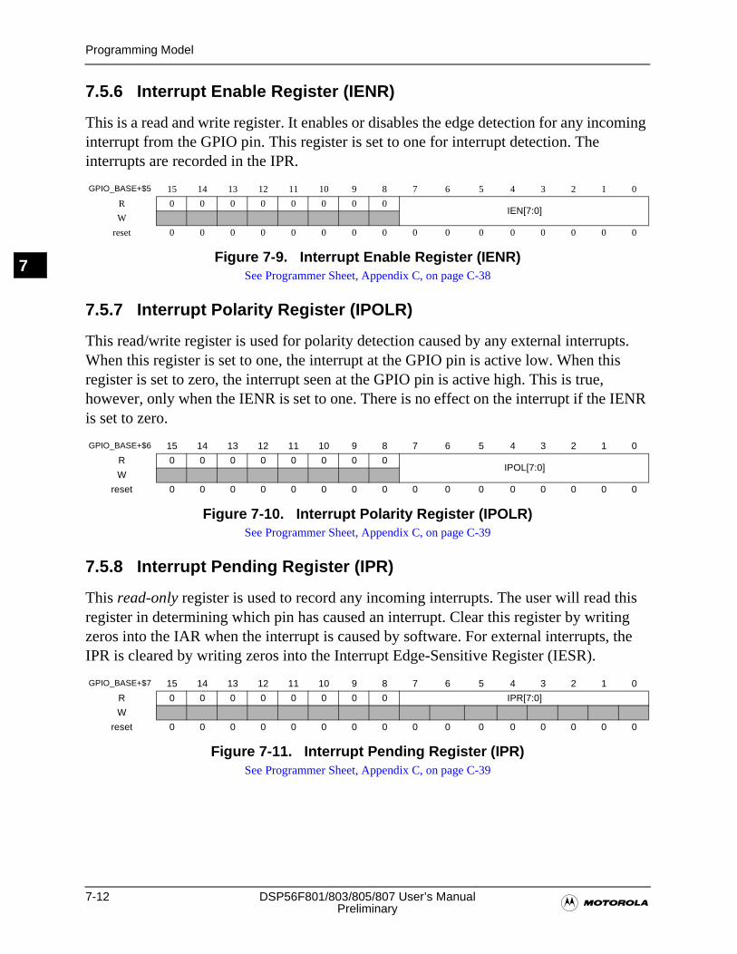
7-12 DSP56F801/803/805/807 User’s Manual�Preliminary
Programming Model
7
7.5.6 Interrupt Enable Register (IENR)
This is a read and write register. It enables or disables the edge detection for any incoming interrupt from the GPIO pin. This register is set to one for interrupt detection. The interrupts are recorded in the IPR.
7.5.7 Interrupt Polarity Register (IPOLR)
This read/write register is used for polarity detection caused by any external interrupts. When this register is set to one, the interrupt at the GPIO pin is active low. When this register is set to zero, the interrupt seen at the GPIO pin is active high. This is true, however, only when the IENR is set to one. There is no effect on the interrupt if the IENR is set to zero.
7.5.8 Interrupt Pending Register (IPR)
This read-only register is used to record any incoming interrupts. The user will read this register in determining which pin has caused an interrupt. Clear this register by writing zeros into the IAR when the interrupt is caused by software. For external interrupts, the IPR is cleared by writing zeros into the Interrupt Edge-Sensitive Register (IESR).
GPIO_BASE+$5 15 14 13 12 11 10 9 8 7 6 5 4 3 2 1 0
R 0 0 0 0 0 0 0 0IEN[7:0]
W
reset 0 0 0 0 0 0 0 0 0 0 0 0 0 0 0 0
Figure 7-9. Interrupt Enable Register (IENR)See Programmer Sheet, Appendix C, on page C-38
GPIO_BASE+$6 15 14 13 12 11 10 9 8 7 6 5 4 3 2 1 0
R 0 0 0 0 0 0 0 0IPOL[7:0]
W
reset 0 0 0 0 0 0 0 0 0 0 0 0 0 0 0 0
Figure 7-10. Interrupt Polarity Register (IPOLR)See Programmer Sheet, Appendix C, on page C-39
GPIO_BASE+$7 15 14 13 12 11 10 9 8 7 6 5 4 3 2 1 0
R 0 0 0 0 0 0 0 0 IPR[7:0]
W
reset 0 0 0 0 0 0 0 0 0 0 0 0 0 0 0 0
Figure 7-11. Interrupt Pending Register (IPR)See Programmer Sheet, Appendix C, on page C-39
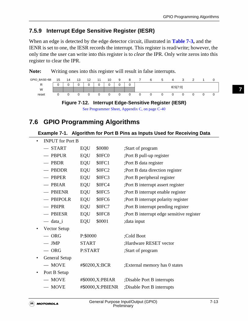
GPIO Programming Algorithms
�General Purpose Input/Output (GPIO) 7-13
Preliminary
7
7.5.9 Interrupt Edge Sensitive Register (IESR)
When an edge is detected by the edge detector circuit, illustrated in Table 7-3, and the IENR is set to one, the IESR records the interrupt. This register is read/write; however, the only time the user can write into this register is to clear the IPR. Only write zeros into this register to clear the IPR.
Note: Writing ones into this register will result in false interrupts.
7.6 GPIO Programming Algorithms
Example 7-1. Algorithm for Port B Pins as Inputs Used for Receiving Data
• INPUT for Port B
— START EQU $0080 ;Start of program
— PBPUR EQU $0FC0 ;Port B pull-up register
— PBDR EQU $0FC1 ;Port B data register
— PBDDR EQU $0FC2 ;Port B data direction register
— PBPER EQU $0FC3 ;Port B peripheral register
— PBIAR EQU $0FC4 ;Port B interrupt assert register
— PBIENR EQU $0FC5 ;Port B interrupt enable register
— PBIPOLR EQU $0FC6 ;Port B interrupt polarity register
— PBIPR EQU $0FC7 ;Port B interrupt pending register
— PBIESR EQU $0FC8 ;Port B interrupt edge sensitive register
— data_i EQU $0001 ;data input
• Vector Setup
— ORG P:$0000 ;Cold Boot
— JMP START ;Hardware RESET vector
— ORG P:START ;Start of program
• General Setup
— MOVE #$0200,X:BCR ;External memory has 0 states
• Port B Setup
— MOVE #$0000,X:PBIAR ;Disable Port B interrupts
— MOVE #$0000,X:PBIENR ;Disable Port B interrupts
GPIO_BASE+$8 15 14 13 12 11 10 9 8 7 6 5 4 3 2 1 0
R 0 0 0 0 0 0 0 0IES[7:0]
W
reset 0 0 0 0 0 0 0 0 0 0 0 0 0 0 0 0
Figure 7-12. Interrupt Edge-Sensitive Register (IESR)See Programmer Sheet, Appendix C, on page C-40
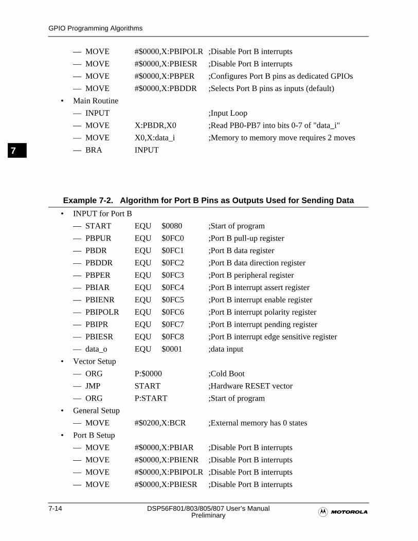
7-14 DSP56F801/803/805/807 User’s Manual�Preliminary
GPIO Programming Algorithms
7
— MOVE #$0000,X:PBIPOLR ;Disable Port B interrupts
— MOVE #$0000,X:PBIESR ;Disable Port B interrupts
— MOVE #$0000,X:PBPER ;Configures Port B pins as dedicated GPIOs
— MOVE #$0000,X:PBDDR ;Selects Port B pins as inputs (default)
• Main Routine
— INPUT ;Input Loop
— MOVE X:PBDR,X0 ;Read PB0-PB7 into bits 0-7 of "data_i"
— MOVE X0,X:data_i ;Memory to memory move requires 2 moves
— BRA INPUT
Example 7-2. Algorithm for Port B Pins as Outputs Used for Sending Data
• INPUT for Port B
— START EQU $0080 ;Start of program
— PBPUR EQU $0FC0 ;Port B pull-up register
— PBDR EQU $0FC1 ;Port B data register
— PBDDR EQU $0FC2 ;Port B data direction register
— PBPER EQU $0FC3 ;Port B peripheral register
— PBIAR EQU $0FC4 ;Port B interrupt assert register
— PBIENR EQU $0FC5 ;Port B interrupt enable register
— PBIPOLR EQU $0FC6 ;Port B interrupt polarity register
— PBIPR EQU $0FC7 ;Port B interrupt pending register
— PBIESR EQU $0FC8 ;Port B interrupt edge sensitive register
— data_o EQU $0001 ;data input
• Vector Setup
— ORG P:$0000 ;Cold Boot
— JMP START ;Hardware RESET vector
— ORG P:START ;Start of program
• General Setup
— MOVE #$0200,X:BCR ;External memory has 0 states
• Port B Setup
— MOVE #$0000,X:PBIAR ;Disable Port B interrupts
— MOVE #$0000,X:PBIENR ;Disable Port B interrupts
— MOVE #$0000,X:PBIPOLR ;Disable Port B interrupts
— MOVE #$0000,X:PBIESR ;Disable Port B interrupts
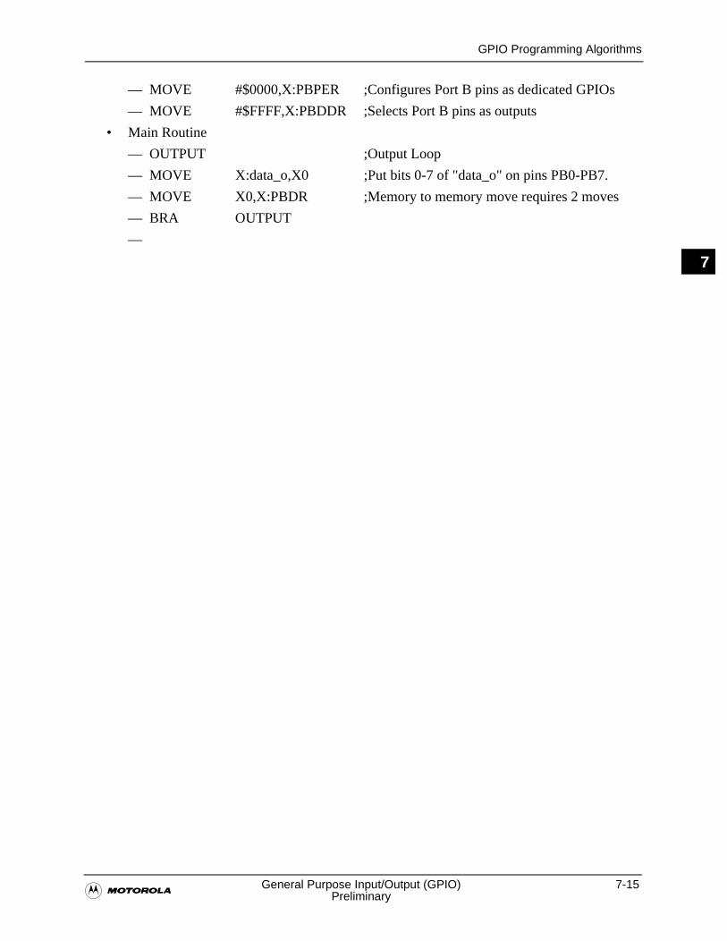
GPIO Programming Algorithms
�General Purpose Input/Output (GPIO) 7-15
Preliminary
7
— MOVE #$0000,X:PBPER ;Configures Port B pins as dedicated GPIOs
— MOVE #$FFFF,X:PBDDR ;Selects Port B pins as outputs
• Main Routine
— OUTPUT ;Output Loop
— MOVE X:data_o,X0 ;Put bits 0-7 of "data_o" on pins PB0-PB7.
— MOVE X0,X:PBDR ;Memory to memory move requires 2 moves
— BRA OUTPUT
—

7-16 DSP56F801/803/805/807 User’s Manual�Preliminary
GPIO Programming Algorithms
7
�Motorola Scalable Controller Area Network (MSCAN) 8-1
Preliminary
8
Chapter 8Motorola Scalable Controller Area
Network (MSCAN)

8-2 DSP56F801/803/805/807 User’s Manual�Preliminary
8
Introduction
�Motorola Scalable Controller Area Network (MSCAN) 8-3
Preliminary
8
8.1 Introduction
The Motorola Scalable Controller Area Network (MSCAN) is available on three of the four DSP core-based family chips: DSP56F803/805/807.
The MSCAN definition is based on the MSCAN12 definition, the specific implementation of the Motorola Scalable CAN concept, originally targeted for the Motorola MC68HC12 Micro controller Family.
The module is a communication controller implementing the CAN 2.0 A/B protocol, as defined in the BOSCH specification dated September 1991. For customers to fully understand the MSCAN specification, we first recommend reading the Bosch specification to familiarize yourself with terms and concepts contained within this document.
The CAN protocol was primarily designed to be a vehicle serial data bus, meeting the specific requirements of that field such as:
• Real-time processing
• Reliable operation in the EMI environment of a vehicle
• Cost-effectiveness
• Required bandwidth
The transmission frames in CAN is similar to the Ethernet protocol, except for different collision avoidance. To send a ready frame, each station listens for the idle bus state. Once it is recognized, each node starts sending its frame. If a node sends a one but reads back a zero, then it stops transmission and goes into the idle listen mode. Each frame is marked by a unique CAN protocol header, so after transmission of 11 bits, 29 for CAN 2.0B, only one node always wins arbitration. The side effect of the CAN arbitration schema is a unique priority for each frame deemed very important for critical processing.
MSCAN utilizes an advanced buffer arrangement resulting in a predictable real-time behavior, simplifying the application software.
8-4 DSP56F801/803/805/807 User’s Manual�Preliminary
Features
8
8.2 Features
Basic features of the MSCAN are:
• Modular architecture
• Implementation of the CAN protocol—Version 2.0A/B
— Standard and extended data frames
— Zero to eight bytes data length
— Programmable bit rate up to 1Mbps
— Support for remote frames
• Double-buffered receive storage scheme
• Triple-buffered transmit storage scheme with internal prioritization using a local priority concept
• Flexible identifier filter capable of masking supports two full-size extended identifier filters: two 32-bit, four 16-bit, or eight 8-bit filters
• Programmable wake-up functionality with integrated low-pass filter
• Programmable Loop Back mode supports self-test operation
• Separate signalling and interrupt capabilities for all CAN receiver and transmitter error states: Warning, Error Passive, Bus-Off
• Programmable MSCAN clock source, either IPBus clock or crystal oscillator output
• Three low power modes: Sleep, Soft Reset and Power Down
8.3 Pin Definitions
The MSCAN uses two external pins: Receive input, MSCAN_RXTransmit output and MSCAN_TX. The MSCAN_TX output pin represents the logic level on the CAN:
• 0 is for a dominant state
• 1 is for a recessive state
When the MSCAN is enabled, (CANE = 1) via the CANCTL1 register, MSCAN_RX is the dedicated input pin and MSCAN_TX is the dedicated output pin, or open-drain output. The MSCAN_RX pin has an internal pull-up.
A typical CAN system with MSCAN is illustrated in Figure 8-1. Each CAN station is connected physically to the CAN bus lines through a transceiver chip. The transceiver is
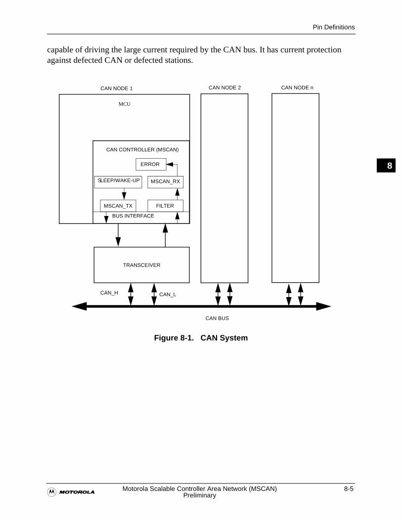
Pin Definitions
�Motorola Scalable Controller Area Network (MSCAN) 8-5
Preliminary
8
capable of driving the large current required by the CAN bus. It has current protection against defected CAN or defected stations.
Figure 8-1. CAN System
CAN BUS
TRANSCEIVER
CAN NODE 1 CAN NODE 2 CAN NODE n
CAN_L
MCU
CAN_H
CAN CONTROLLER (MSCAN)
BUS INTERFACE
MSCAN_TX
MSCAN_RXLEEP/WAKE-UP
ERROR
FILTER
S
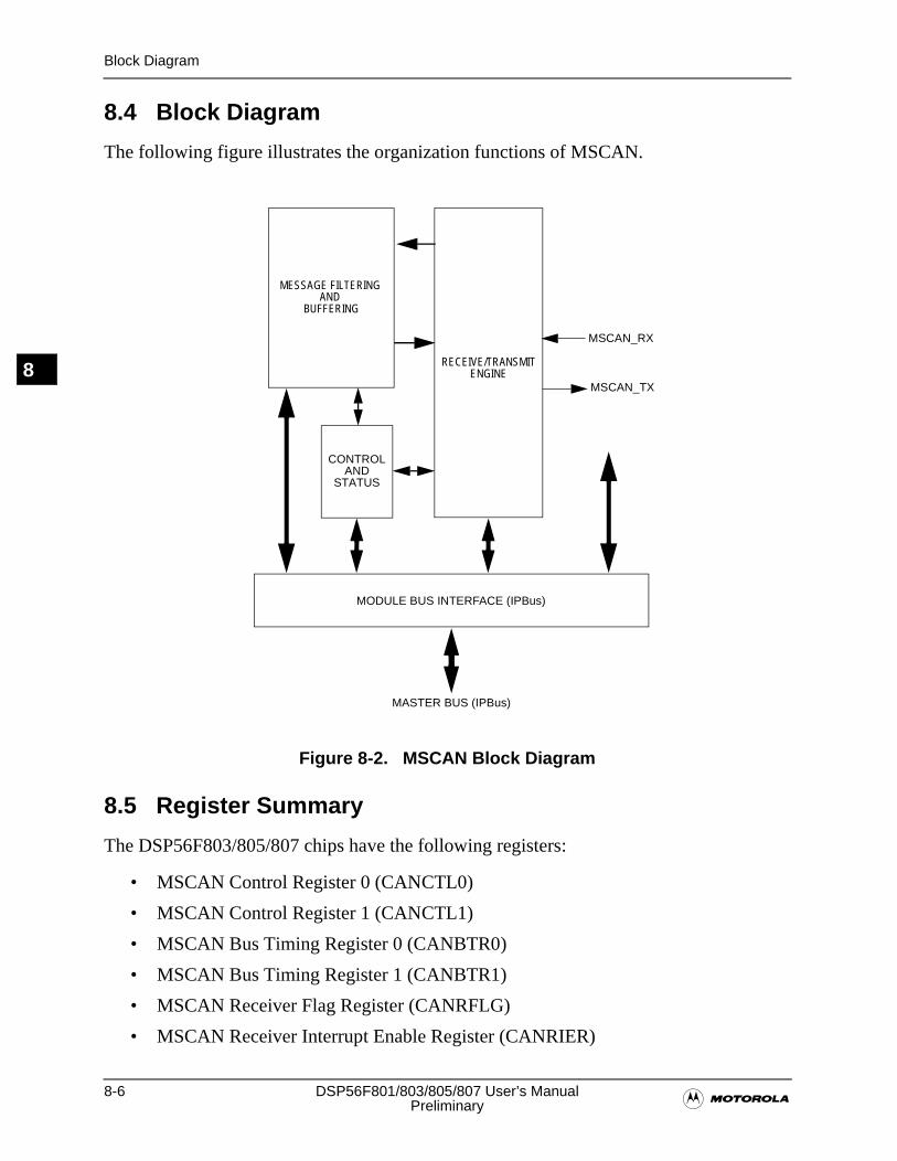
8-6 DSP56F801/803/805/807 User’s Manual�Preliminary
Block Diagram
8
8.4 Block Diagram
The following figure illustrates the organization functions of MSCAN.
Figure 8-2. MSCAN Block Diagram
8.5 Register Summary
The DSP56F803/805/807 chips have the following registers:
• MSCAN Control Register 0 (CANCTL0)
• MSCAN Control Register 1 (CANCTL1)
• MSCAN Bus Timing Register 0 (CANBTR0)
• MSCAN Bus Timing Register 1 (CANBTR1)
• MSCAN Receiver Flag Register (CANRFLG)
• MSCAN Receiver Interrupt Enable Register (CANRIER)
MESSAGE FILTERING
MODULE BUS INTERFACE (IPBus)
MASTER BUS (IPBus)
RECEIVE/TRANSMITENGINE
AND BUFFERING
CONTROLAND
STATUS
MSCAN_RX
MSCAN_TX
Register Map
�Motorola Scalable Controller Area Network (MSCAN) 8-7
Preliminary
8
• MSCAN Transmitter Flag Register (CANTFLG)
• MSCAN Transmitter Control Register (CANTCR)
• Identifier Acceptance Control Register (CANIDAC)
• MSCAN Receiver Error Counter Register (CANRXERR)
• MSCAN Transmit Error Counter Register (CANTXERR)
• MSCAN Identifier Acceptance Registers (CANIDAR0–7)
• MSCAN Identifier Mask Registers (CANIDMR0–7)
• MSCAN Receive Buffer Identifier Registers 0–3 (CAN_RB_IDR0–3)
• MSCAN Receive Buffer Data Segment Registers 0–7 (CAN_RB_DSR0–7)
• MSCAN Receive Buffer Data Length Register (CAN_RB_DLR)
• MSCAN Receive Buffer Priority Register (CAN_RB_TBPR)
• MSCAN Transmit Buffer 0 Identifier Registers 0–3 (CAN_TB0_IDR0–3)
• MSCAN Transmit Buffer 0 Data Segment Registers 0–7(CAN_TB0_DSR0–7)
• MSCAN Transmit Buffer 0 Data Length Register (CAN_TB0_DLR)
• MSCAN Transmit Buffer 0 Transmit Buffer Priority Register (CAN_TB0_TBPR)
• MSCAN Transmit Buffer 1 Identifier Registers 0–3 (CAN_TB1_IDR0–3)
• MSCAN Transmit Buffer 1 Data Segment Registers 0–7 (CAN_TB1_DSR0–7)
• MSCAN Transmit Buffer 1 Data Length Register (CAN_TB1_DLR)
• MSCAN Transmit Buffer 1 Transmit Buffer Priority Register (CAN_TB1_TBPR)
• MSCAN Transmit Buffer 2 Identifier Registers 0–3 (CAN_TB2_IDR0–3)
• MSCAN Transmit Buffer 2 Data Segment Registers 0–7 (CAN_TB2_DSR0–7)
• MSCAN Transmit Buffer 2 Data Length Register (CAN_TB2_DLR)
• MSCAN Transmit Buffer 2 Transmit Buffer Priority Register (CAN_TB2_TBPR)
8.6 Register Map
The MSCAN occupies 128 words in the memory space starting at CAN_BASE, defined in Table 3-11. The register decode map is fixed, beginning at the first address of the module address offset. Figure 8-3 illustrates the organization of the registers.
Note: All MSCAN registers are implemented as 16-bit with the most significant eight bits tied to zero. Therefore, users should note the lower eight significant bits are the relevant configuration of status bits to be used.
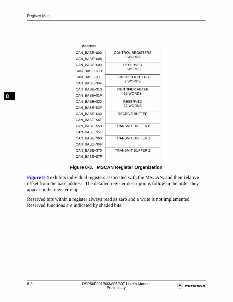
8-8 DSP56F801/803/805/807 User’s Manual�Preliminary
Register Map
8
Figure 8-3. MSCAN Register Organization
Figure 8-4 exhibits individual registers associated with the MSCAN, and their relative offset from the base address. The detailed register descriptions follow in the order they appear in the register map.
Reserved bits within a register always read as zero and a write is not implemented. Reserved functions are indicated by shaded bits.
Address
CAN_BASE+$00 CONTROL REGISTERS9 WORDSCAN_BASE+$08
CAN_BASE+$09 RESERVED5 WORDSCAN_BASE+$0D
CAN_BASE+$0E ERROR COUNTERS2 WORDSCAN_BASE+$0F
CAN_BASE+$10 IDENTIFIER FILTER16 WORDSCAN_BASE+$1F
CAN_BASE+$20 RESERVED32 WORDSCAN_BASE+$3F
CAN_BASE+$40 RECEIVE BUFFER
CAN_BASE+$4F
CAN_BASE+$50 TRANSMIT BUFFER 0
CAN_BASE+$5F
CAN_BASE+$60 TRANSMIT BUFFER 1
CAN_BASE+$6F
CAN_BASE+$70 TRANSMIT BUFFER 2
CAN_BASE+$7F
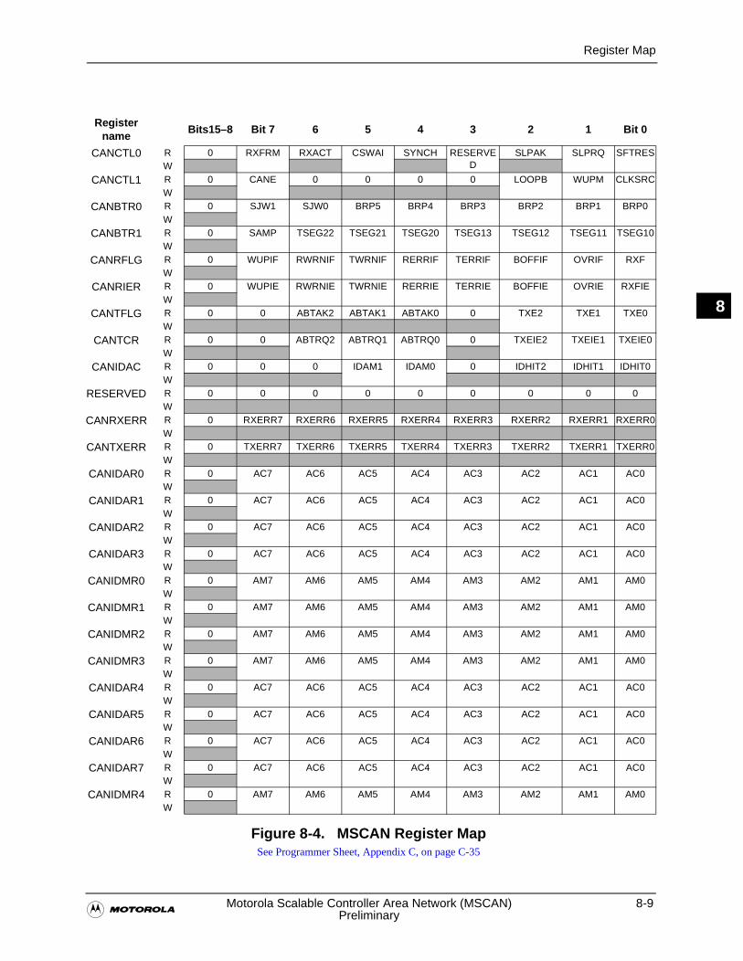
Register Map
�Motorola Scalable Controller Area Network (MSCAN) 8-9
Preliminary
8
Register name
Bits15–8 Bit 7 6 5 4 3 2 1 Bit 0
CANCTL0 R 0 RXFRM RXACT CSWAI SYNCH RESERVED
SLPAK SLPRQ SFTRESW
CANCTL1 R 0 CANE 0 0 0 0 LOOPB WUPM CLKSRCW
CANBTR0 R 0 SJW1 SJW0 BRP5 BRP4 BRP3 BRP2 BRP1 BRP0W
CANBTR1 R 0 SAMP TSEG22 TSEG21 TSEG20 TSEG13 TSEG12 TSEG11 TSEG10W
CANRFLG R 0 WUPIF RWRNIF TWRNIF RERRIF TERRIF BOFFIF OVRIF RXFW
CANRIER R 0 WUPIE RWRNIE TWRNIE RERRIE TERRIE BOFFIE OVRIE RXFIEW
CANTFLG R 0 0 ABTAK2 ABTAK1 ABTAK0 0 TXE2 TXE1 TXE0W
CANTCR R 0 0 ABTRQ2 ABTRQ1 ABTRQ0 0 TXEIE2 TXEIE1 TXEIE0W
CANIDAC R 0 0 0 IDAM1 IDAM0 0 IDHIT2 IDHIT1 IDHIT0W
RESERVED R 0 0 0 0 0 0 0 0 0W
CANRXERR R 0 RXERR7 RXERR6 RXERR5 RXERR4 RXERR3 RXERR2 RXERR1 RXERR0W
CANTXERR R 0 TXERR7 TXERR6 TXERR5 TXERR4 TXERR3 TXERR2 TXERR1 TXERR0W
CANIDAR0 R 0 AC7 AC6 AC5 AC4 AC3 AC2 AC1 AC0W
CANIDAR1 R 0 AC7 AC6 AC5 AC4 AC3 AC2 AC1 AC0W
CANIDAR2 R 0 AC7 AC6 AC5 AC4 AC3 AC2 AC1 AC0W
CANIDAR3 R 0 AC7 AC6 AC5 AC4 AC3 AC2 AC1 AC0W
CANIDMR0 R 0 AM7 AM6 AM5 AM4 AM3 AM2 AM1 AM0W
CANIDMR1 R 0 AM7 AM6 AM5 AM4 AM3 AM2 AM1 AM0W
CANIDMR2 R 0 AM7 AM6 AM5 AM4 AM3 AM2 AM1 AM0W
CANIDMR3 R 0 AM7 AM6 AM5 AM4 AM3 AM2 AM1 AM0W
CANIDAR4 R 0 AC7 AC6 AC5 AC4 AC3 AC2 AC1 AC0W
CANIDAR5 R 0 AC7 AC6 AC5 AC4 AC3 AC2 AC1 AC0W
CANIDAR6 R 0 AC7 AC6 AC5 AC4 AC3 AC2 AC1 AC0W
CANIDAR7 R 0 AC7 AC6 AC5 AC4 AC3 AC2 AC1 AC0W
CANIDMR4 R 0 AM7 AM6 AM5 AM4 AM3 AM2 AM1 AM0W
Figure 8-4. MSCAN Register Map See Programmer Sheet, Appendix C, on page C-35
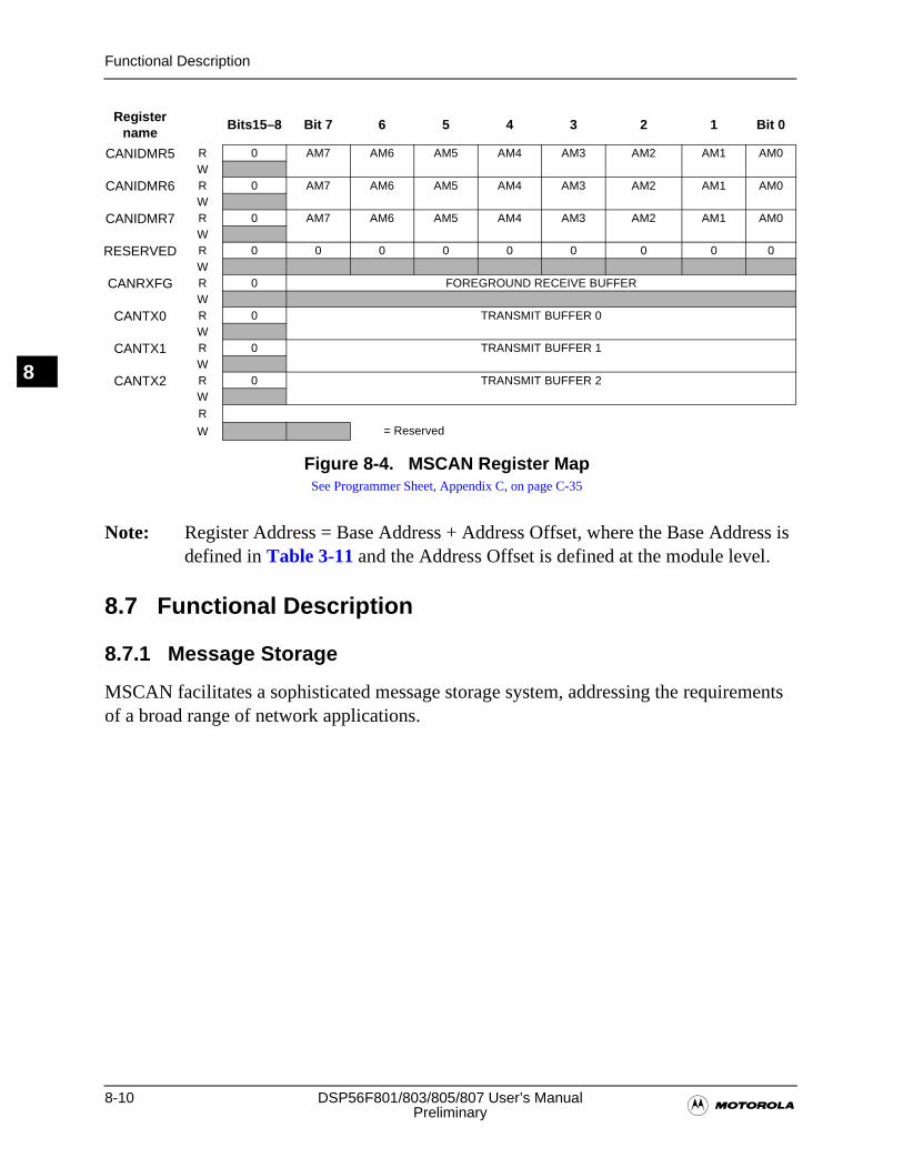
8-10 DSP56F801/803/805/807 User’s Manual�Preliminary
Functional Description
8
Note: Register Address = Base Address + Address Offset, where the Base Address is defined in Table 3-11 and the Address Offset is defined at the module level.
8.7 Functional Description
8.7.1 Message Storage
MSCAN facilitates a sophisticated message storage system, addressing the requirements of a broad range of network applications.
CANIDMR5 R 0 AM7 AM6 AM5 AM4 AM3 AM2 AM1 AM0W
CANIDMR6 R 0 AM7 AM6 AM5 AM4 AM3 AM2 AM1 AM0W
CANIDMR7 R 0 AM7 AM6 AM5 AM4 AM3 AM2 AM1 AM0W
RESERVED R 0 0 0 0 0 0 0 0 0W
CANRXFG R 0 FOREGROUND RECEIVE BUFFERW
CANTX0 R 0 TRANSMIT BUFFER 0W
CANTX1 R 0 TRANSMIT BUFFER 1W
CANTX2 R 0 TRANSMIT BUFFER 2W
R
W = Reserved
Register name
Bits15–8 Bit 7 6 5 4 3 2 1 Bit 0
Figure 8-4. MSCAN Register Map See Programmer Sheet, Appendix C, on page C-35
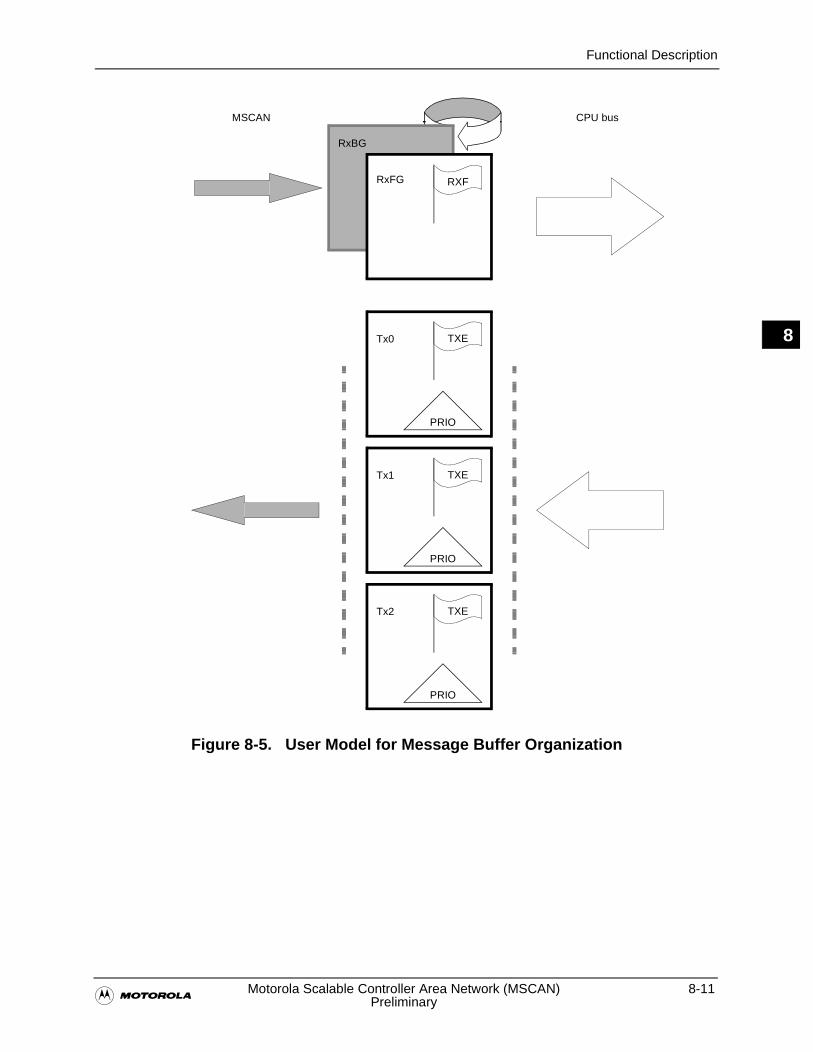
Functional Description
�Motorola Scalable Controller Area Network (MSCAN) 8-11
Preliminary
8
Figure 8-5. User Model for Message Buffer Organization
RxFG
RxBG
Tx0
RXF
TXE
PRIO
Tx1 TXE
PRIO
Tx2 TXE
PRIO
MSCAN CPU bus
8-12 DSP56F801/803/805/807 User’s Manual�Preliminary
Functional Description
8
8.7.1.1 Message Transmit Background
Modern application layer software is built upon two fundamental assumptions:
1. Any CAN node is able to send out a stream of scheduled messages without releasing the bus between the two messages. Such nodes arbitrate for the bus immediately after sending the previous message and only release the bus in case of lost arbitration.
2. The internal message queue within any CAN node is organized so the highest priority message is sent out first when more than one message is ready to be sent.
The above behavior cannot be achieved with a single transmit buffer. That buffer must be reloaded immediately after the previous message is sent. The loading process lasts a finite amount of time. It must be completed within the Inter-Frame Sequence (IFS)1 in order to send an uninterrupted stream of messages. Even if this is feasible for limited CAN bus speeds, it requires the CPU react with short latencies to the transmit interrupt.
A double-buffer scheme uncouples the reloading of the transmit buffer from the actual message sending thereby reducing the reactiveness requirements on the CPU. It is possible problems could arise if a sent message has finished while the CPU is reloading the second buffer. In this instance there would be no buffer ready for transmission, releasing the bus.
At least three transmit buffers are required to meet the first of the above requirements under all circumstances. The MSCAN has three transmit buffers.
The second requirement calls for internal MSCAN prioritization, implementing the local priority concept described in the next section.
8.7.1.2 Transmit Structures
The MSCAN has a triple transmit buffer scheme. The transmit scheme allows multiple messages to be established in advance, achieving an optimized real-time performance. The three buffers are arranged as shown in Figure 8-5.
All three buffers have a 13-byte data structure similar to the outline of the receive buffers. See Section 8.8.14. An additional Transmit Buffer Priority Register (TBPR) contains an 8-bit Local Priority field (PRIO). See Section 8.8.14.4.
To transmit a message, the CPU must identify an available transmit buffer indicated by a set Transmitter Buffer Empty (TXE[2:0]) Flag. See Section 8.8.7.
1. Reference the Bosch CAN 2.0A/B protocol specification dated September 1991

Functional Description
�Motorola Scalable Controller Area Network (MSCAN) 8-13
Preliminary
8
The CPU then stores the identifier, the control bits, and the data content into one of the transmit buffers. Finally, the buffer is flagged as ready for transmission by clearing the associated TXE Flag.
Next, the MSCAN schedules the message for transmission, and signals the successful transmission of the buffer by setting the associated TXE Flag. A transmit interrupt is generated2 when TXE[2:0] is set and can be used to drive the application software to re-load the buffer. Refer to Section 8.11.
If more than one buffer is scheduled for transmission when the CAN bus becomes available for arbitration, the MSCAN uses the local priority setting of the three buffers to determine the prioritization. For this purpose, every transmit buffer has an 8-bit PRIO. The application software programs this field when the message is set up. The local priority reflects the order of this particular message relative to the set of messages being transmitted from this node. The lowest binary value of the PRIO is defined to be the highest priority. The internal scheduling process takes place whenever the MSCAN arbitrates for the bus. This is also the case after the occurrence of a transmission error.
When a high priority message is scheduled by the application software, it may become necessary to quit a lower priority, not yet transmitted message, in one of the three transmit buffers. Messages already in transmission cannot be aborted, so the user must request the termination by setting the corresponding Abort Request bit (ABTRQ). See Section 8.8.8. The MSCAN then permits the request, if possible, by:
1. Setting the corresponding Abort Acknowledge Flag (ABTAK) in the CANTFLG register
2. Setting the associated TXE Flag to release the buffer
3. Generating a transmit interrupt
The transmit interrupt handler software can tell from the setting of the ABTAK Flag whether the message was aborted (ABTAK = 1) or sent (ABTAK = 0)
8.7.1.3 Receive Structures
Received messages are stored in a two stage input FIFO. The two message buffers are alternately mapped into a single memory area. See Figure 8-5. While the Background Receive Buffer (RxBG) is exclusively associated with the MSCAN, the Foreground Receive Buffer (RxFG) is addressed by the CPU. This scheme simplifies the handler software because only one address area is applicable for the receive process. Users cannot read/write to the RxBG buffer.
2. The transmit interrupt occurs only if not masked. A polling scheme can be applied on TXEx also.
8-14 DSP56F801/803/805/807 User’s Manual�Preliminary
Functional Description
8
Both buffers have a size of 13 bytes for storage of the CAN control bits, the identifier, standard or extended, and the data contents. See details in Section 8.8.14.3
The Receiver Full Flag (RXF) signals the status of the foreground receive buffer. See Section 8.8.5. A flag is set when the buffer contains a correctly received message with a matching identifier.
Each message is checked to see if it passes the reception filter. See Section 8.7.1.4. It is written into parallel RxBG. MSCAN copies the content of RxBG into RxFG,4 sets the RXF Flag, and generates a receive interrupt to the CPU.5 See Section 8.11. Receive handler will read the received message from RxFG, before resetting the RXF Flag. Reset of the RXF Flag acknowledges the interrupt, in order to release the foreground buffer. A new message, can follow immediately after the IFS field of the CAN frame is received into RxBG. The over-writing of the background buffer is independent of the identifier filter function.
When the MSCAN module is transmitting, the MSCAN receives its own transmitted messages into the background receive buffer RxBG. However, it does not overwrite RxFG, nor generate a receive interrupt, nor acknowledge its own messages on the CAN bus.
There is an exception to this rule. It is in Loop Back mode where the MSCAN treats its own messages exactly like all other incoming messages. See Section 8.8.3. The MSCAN receives its own transmitted messages in the event it loses arbitration.6 If arbitration is lost, the MSCAN must be prepared to become a receiver.
An overrun condition occurs when both message buffers are filled. Overrun messages are discarded, indicating an Error Interrupt. The MSCAN is still able to transmit messages with both receive message buffers filled; however, all incoming messages are discarded. See Section 8.11.
8.7.1.4 Identifier Acceptance Filter
The MSCAN Identifier Acceptance Registers define the acceptable patterns of the standard or extended identifier, ID[10:0] or ID[28:0] bits. See Section 8.8.12. Any of these bits can be marked don’t care in the MSCAN Identifier Mask Registers. See Section 8.8.13.
A filter hit is indicated to the application software by a set Receive Buffer Full Flag
3. Reference the Bosch CAN 2.0A/B protocol specification dated September 1991 for details4. Only if the RXF Flag is not set5. The receive interrupt occurs only if not masked. A polling scheme can be applied on RXF also.6. Reference the Bosch CAN 2.0A/B protocol specification dated September 1991 for details
Functional Description
�Motorola Scalable Controller Area Network (MSCAN) 8-15
Preliminary
8
(RXF = 1) and three bits in the CANIDAC register. See Section 8.8.9. These Identifier Hit F Flags, IDHIT[2:0], clearly identify the filter section causing the acceptance. They simplify the application software’s task to identify the cause of the receiver interrupt. In case more than one hit occurs, two or more filters match, the lower hit has priority.
A very flexible, programmable, and generic identifier acceptance filter has been introduced reducing the CPU Interrupt loading. The filter is programmable to operate in four different modes:7
• Two identifier acceptance filters, each to be applied to
— The full 29 bits of the extended identifier and to the following bits of the CAN 2.0B frame: Remote Transmission Request (RTR), Identifier Extension (IDE), and Substitute Remote Request (SRR)
— The 11 bits of the standard identifier plus the RTR and IDE bits of the CAN 2.0A/B messages. This mode implements two filters for a full length CAN 2.0B-compliant extended identifier 8
Figure 8-6 illustrates how the first 32-bit filter bank, CANIDAR0–3 and CANIDMR0–3, produces a filter zero hit. Similarly, the second filter bank, CANIDAR4–7 and CANIDMR4–7, produces a filter one hit
• Four identifier acceptance filters, each to be applied to
— The 14MSBs of the extended identifier plus the SRR and IDE bits of CAN 2.0B messages
— The 11 bits of the standard identifier, the RTR and IDE bits of CAN 2.0A/B messages
Figure 8-7 illustrates how the first 32-bit filter bank, CANIDAR0–3 and CANIDMR0–3, produces filter zero and one hit. Similarly, the second filter bank, CANIDAR4–7 and CANIDMR4–7, produces filter two and three hits
• Eight identifier acceptance filters, each to be applied to the first eight bits of the identifier. This mode implements eight independent filters for the first eight bits of a CAN 2.0B-compliant standard identifier or a CAN 2.0B-compliant extended identifier. Figure 8-8 displays how the first 32-bit filter bank, CANIDAR0–3 and CANIDMR0–3, produces filter zero to three hits. Similarly, the second filter bank, CANIDAR4–7 and CANIDMR4–7, produces filter four to seven hits
7. For a better understanding of references made within the filter mode description, reference the Bosch specification dated September 1991 which details the CAN 2.0A/B protocol.8. Although this mode can be used for standard identifiers, it is recommended to use the four or eight iden-tifier acceptance filters for standard identifiers
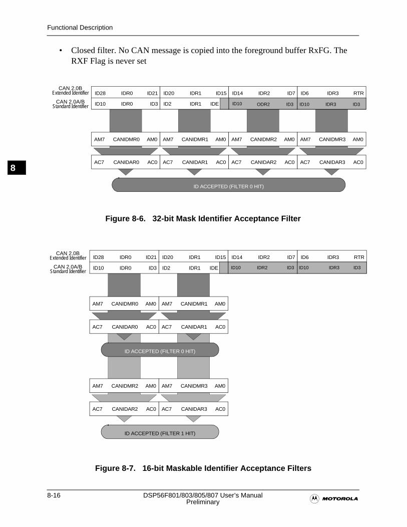
8-16 DSP56F801/803/805/807 User’s Manual�Preliminary
Functional Description
8
• Closed filter. No CAN message is copied into the foreground buffer RxFG. The RXF Flag is never set
Figure 8-6. 32-bit Mask Identifier Acceptance Filter
Figure 8-7. 16-bit Maskable Identifier Acceptance Filters
ID28 ID21IDR0
ID10 ID3IDR0
ID20 ID15IDR1
ID2 IDEIDR1
ID14 ID7IDR2
ID10 ID3IDR2
ID6 RTRIDR3
ID10 ID3IDR3
AC7 AC0CANIDAR0
AM7 AM0CANIDMR0
AC7 AC0CANIDAR1
AM7 AM0CANIDMR1
AC7 AC0CANIDAR2
AM7 AM0CANIDMR2
AC7 AC0CANIDAR3
AM7 AM0CANIDMR3
ID ACCEPTED (FILTER 0 HIT)
CAN 2.0BExtended Identifier
CAN 2.0A/BStandard Identifier ID10 ODR2 ID3 ID10 IDR3 ID3
ID28 ID21IDR0
ID10 ID3IDR0
ID20 ID15IDR1
ID2 IDEIDR1
ID14 ID7IDR2
ID10 ID3IDR2
ID6 RTRIDR3
ID10 ID3IDR3
AC7 AC0CANIDAR0
AM7 AM0CANIDMR0
AC7 AC0CANIDAR1
AM7 AM0CANIDMR1
ID ACCEPTED (FILTER 0 HIT)
AC7 AC0CANIDAR2
AM7 AM0CANIDMR2
AC7 AC0CANIDAR3
AM7 AM0CANIDMR3
ID ACCEPTED (FILTER 1 HIT)
CAN 2.0BExtended Identifier
CAN 2.0A/BStandard Identifier
ID10 ID10IDR2 IDR3 ID3ID3
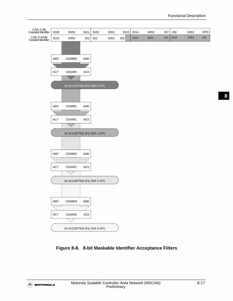
Functional Description
�Motorola Scalable Controller Area Network (MSCAN) 8-17
Preliminary
8
Figure 8-8. 8-bit Maskable Identifier Acceptance Filters
CAN 2.0BExtended Identifier
CAN 2.0A/BStandard Identifier
AC7 AC0CIDAR3
AM7 AM0CIDMR3
ID ACCEPTED (FILTER 3 HIT)
AC7 AC0CIDAR2
AM7 AM0CIDMR2
ID ACCEPTED (FILTER 2 HIT)
AC7 AC0CIDAR1
AM7 AM0CIDMR1
ID ACCEPTED (FILTER 1 HIT)
ID28 ID21IDR0
ID10 ID3IDR0
ID20 ID15IDR1
ID2 IDEIDR1
ID14 ID7IDR2
ID10 ID3IDR2
ID6 RTRIDR3
ID10 ID3IDR3
AC7 AC0CIDAR0
AM7 AM0CIDMR0
ID ACCEPTED (FILTER 0 HIT)
ID10 IDR2 ID10ID3 IDR3 ID3
8-18 DSP56F801/803/805/807 User’s Manual�Preliminary
Functional Description
8
8.7.2 Protocol Violation Protection
MSCAN protects from accidentally violating the CAN protocol through programming errors. The protection logic implements the following features:
• Receive and transmit error counters cannot be modified or otherwise manipulated
• Registers controlling the configuration of the MSCAN cannot be modified while the MSCAN is on-line. The SFTRES bit in the CANCTL0 register serves as a lock protecting the following registers: See Section 8.8.1
— MSCAN Control One Register, CANCTL1
— MSCAN Bus Timing Registers Zero and One, CANBTR0, CANBTR1
— MSCAN Identifier Acceptance Control Register, CANIDAC
— MSCAN Identifier Acceptance Registers, CANIDAR0–7
— MSCAN Identifier Mask Registers, CANIDMR0–7
• The MSCAN_TX pin is forced to a recessive state when the MSCAN goes into any of the low power modes. See Section 8.10.4 through Section 8.10.6
• MSCAN_TX pin is an Open-Drain output. System designer using CAN should have external pull-up on MSCAN_TX
• MSCAN_RX input has an internal pull-up
• As further protection against inadvertently disabling the MSCAN, the enable bit, CANE, is only write-capable once in normal modes
8.7.3 Clock System
Figure 8-9 illustrates the structure of the MSCAN clock generation circuitry. With this flexible clocking scheme, the MSCAN is able to handle CAN bus rates ranging from 10 Kbps up to 1Mbps.
The Clock Source bit, CLKSRC, in the CANCTL1 register defines whether the MSCAN is connected to the output of the crystal oscillator, EXTALi, or to the IPBus Clock. See Section 8.8.2. The muxing of these two clocks is performed inside MSCAN. The clock source and generation must be selected to meet the tight oscillator tolerance requirements of the CAN protocol, up to 0.4 percent accumulated jitter. Additionally, for high CAN bus rates of 1Mbps, a 50 percent duty cycle of the clock is required. This is guaranteed when using the IPBus clock.
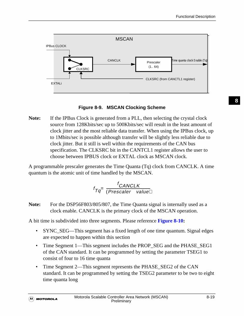
Functional Description
�Motorola Scalable Controller Area Network (MSCAN) 8-19
Preliminary
8Figure 8-9. MSCAN Clocking Scheme
Note: If the IPBus Clock is generated from a PLL, then selecting the crystal clock source from 128Kbits/sec up to 500Kbits/sec will result in the least amount of clock jitter and the most reliable data transfer. When using the IPBus clock, up to 1Mbits/sec is possible although transfer will be slightly less reliable due to clock jitter. But it still is well within the requirements of the CAN bus specification. The CLKSRC bit in the CANTCL1 register allows the user to choose between IPBUS clock or EXTAL clock as MSCAN clock.
A programmable prescaler generates the Time Quanta (Tq) clock from CANCLK. A time quantum is the atomic unit of time handled by the MSCAN.
Note: For the DSP56F803/805/807, the Time Quanta signal is internally used as a clock enable. CANCLK is the primary clock of the MSCAN operation.
A bit time is subdivided into three segments. Please reference Figure 8-10:
• SYNC_SEG—This segment has a fixed length of one time quantum. Signal edges are expected to happen within this section
• Time Segment 1—This segment includes the PROP_SEG and the PHASE_SEG1 of the CAN standard. It can be programmed by setting the parameter TSEG1 to consist of four to 16 time quanta
• Time Segment 2—This segment represents the PHASE_SEG2 of the CAN standard. It can be programmed by setting the TSEG2 parameter to be two to eight time quanta long
Prescaler(1.. 64)
CLKSRC
CANCLK Time quanta clock Enable (Tq)
IPBus CLOCK
EXTALiCLKSRC (from CANCTL1 register)
MSCAN
fTq
fCANCLKPrescaler valueÞ( )
-------------------------------------------------------=
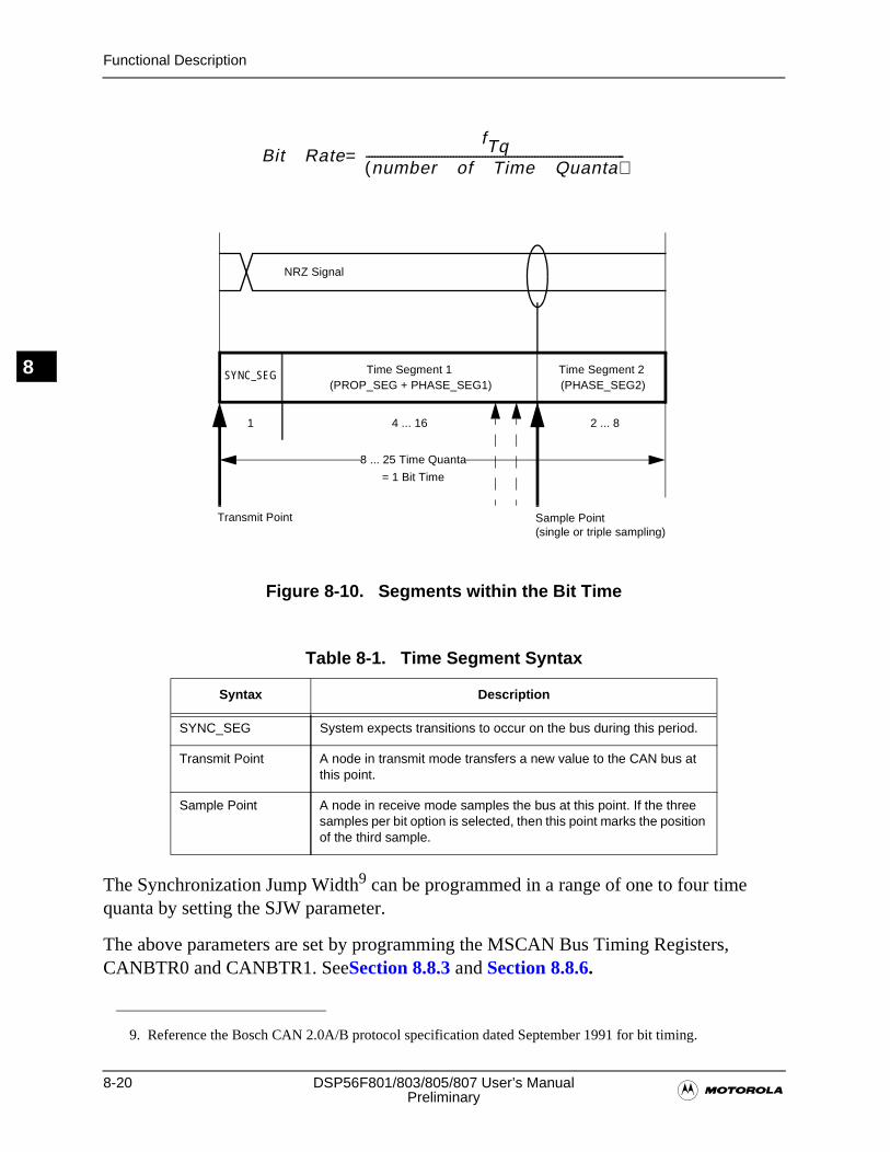
8-20 DSP56F801/803/805/807 User’s Manual�Preliminary
Functional Description
8
Figure 8-10. Segments within the Bit Time
The Synchronization Jump Width9 can be programmed in a range of one to four time quanta by setting the SJW parameter.
The above parameters are set by programming the MSCAN Bus Timing Registers, CANBTR0 and CANBTR1. SeeSection 8.8.3 and Section 8.8.6.
Table 8-1. Time Segment Syntax
Syntax Description
SYNC_SEG System expects transitions to occur on the bus during this period.
Transmit Point A node in transmit mode transfers a new value to the CAN bus at this point.
Sample Point A node in receive mode samples the bus at this point. If the three samples per bit option is selected, then this point marks the position of the third sample.
9. Reference the Bosch CAN 2.0A/B protocol specification dated September 1991 for bit timing.
Bit RatefTq
number of Time QuantaÞ Þ Þ( )-----------------------------------------------------------------------------------------=Þ
SYNC_SEG Time Segment 1 Time Segment 2
1 4 ... 16 2 ... 8
8 ... 25 Time Quanta
= 1 Bit Time
NRZ Signal
Sample Point (single or triple sampling)
(PROP_SEG + PHASE_SEG1) (PHASE_SEG2)
Transmit Point
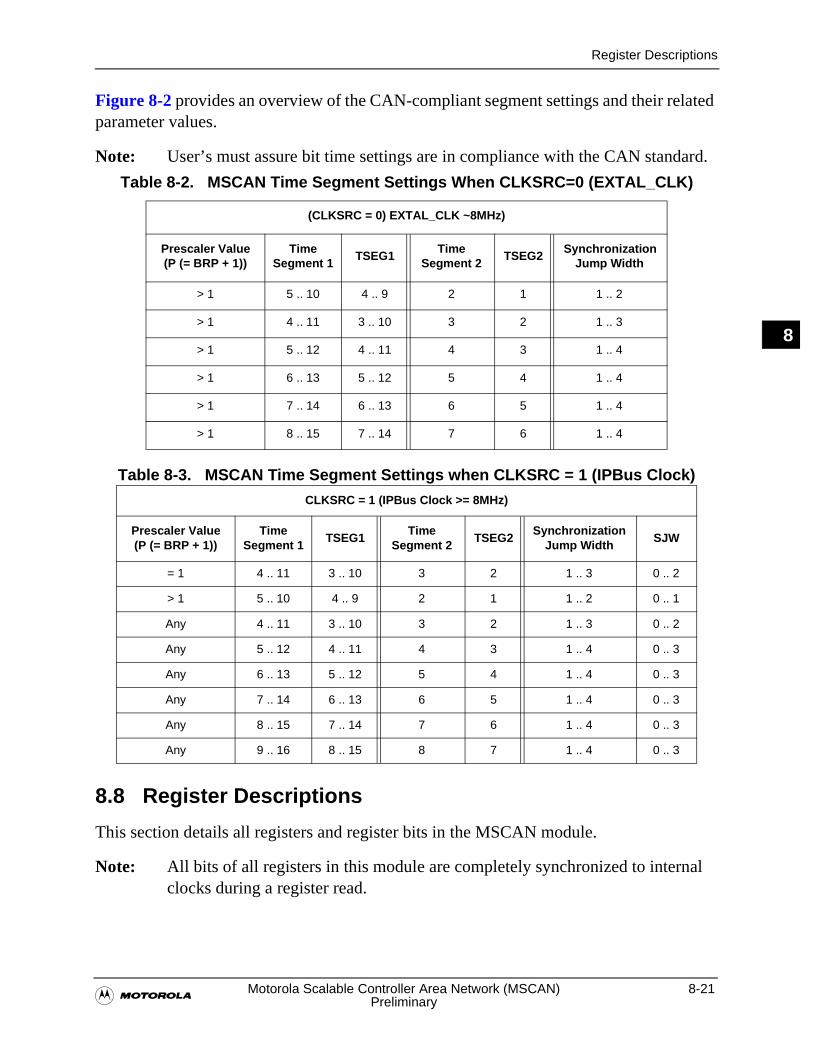
Register Descriptions
�Motorola Scalable Controller Area Network (MSCAN) 8-21
Preliminary
8
Figure 8-2 provides an overview of the CAN-compliant segment settings and their related parameter values.
Note: User’s must assure bit time settings are in compliance with the CAN standard.
Table 8-3. MSCAN Time Segment Settings when CLKSRC = 1 (IPBus Clock)
8.8 Register Descriptions
This section details all registers and register bits in the MSCAN module.
Note: All bits of all registers in this module are completely synchronized to internal clocks during a register read.
Table 8-2. MSCAN Time Segment Settings When CLKSRC=0 (EXTAL_CLK)
(CLKSRC = 0) EXTAL_CLK ~8MHz)
Prescaler Value(P (= BRP + 1))
Time Segment 1
TSEG1Time
Segment 2TSEG2
Synchronization Jump Width
> 1 5 .. 10 4 .. 9 2 1 1 .. 2
> 1 4 .. 11 3 .. 10 3 2 1 .. 3
> 1 5 .. 12 4 .. 11 4 3 1 .. 4
> 1 6 .. 13 5 .. 12 5 4 1 .. 4
> 1 7 .. 14 6 .. 13 6 5 1 .. 4
> 1 8 .. 15 7 .. 14 7 6 1 .. 4
CLKSRC = 1 (IPBus Clock >= 8MHz)
Prescaler Value(P (= BRP + 1))
Time Segment 1
TSEG1Time
Segment 2TSEG2
Synchronization Jump Width
SJW
= 1 4 .. 11 3 .. 10 3 2 1 .. 3 0 .. 2
> 1 5 .. 10 4 .. 9 2 1 1 .. 2 0 .. 1
Any 4 .. 11 3 .. 10 3 2 1 .. 3 0 .. 2
Any 5 .. 12 4 .. 11 4 3 1 .. 4 0 .. 3
Any 6 .. 13 5 .. 12 5 4 1 .. 4 0 .. 3
Any 7 .. 14 6 .. 13 6 5 1 .. 4 0 .. 3
Any 8 .. 15 7 .. 14 7 6 1 .. 4 0 .. 3
Any 9 .. 16 8 .. 15 8 7 1 .. 4 0 .. 3
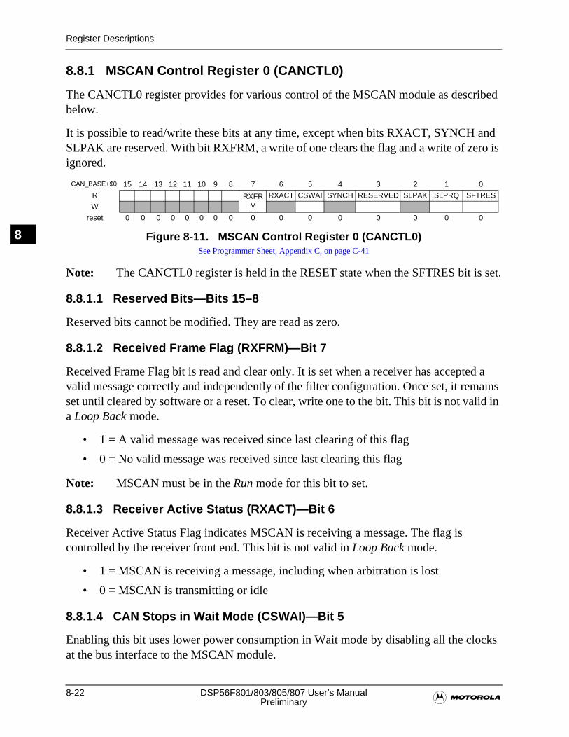
8-22 DSP56F801/803/805/807 User’s Manual�Preliminary
Register Descriptions
8
8.8.1 MSCAN Control Register 0 (CANCTL0)
The CANCTL0 register provides for various control of the MSCAN module as described below.
It is possible to read/write these bits at any time, except when bits RXACT, SYNCH and SLPAK are reserved. With bit RXFRM, a write of one clears the flag and a write of zero is ignored.
Note: The CANCTL0 register is held in the RESET state when the SFTRES bit is set.
8.8.1.1 Reserved Bits—Bits 15–8
Reserved bits cannot be modified. They are read as zero.
8.8.1.2 Received Frame Flag (RXFRM)—Bit 7
Received Frame Flag bit is read and clear only. It is set when a receiver has accepted a valid message correctly and independently of the filter configuration. Once set, it remains set until cleared by software or a reset. To clear, write one to the bit. This bit is not valid in a Loop Back mode.
• 1 = A valid message was received since last clearing of this flag
• 0 = No valid message was received since last clearing this flag
Note: MSCAN must be in the Run mode for this bit to set.
8.8.1.3 Receiver Active Status (RXACT)—Bit 6
Receiver Active Status Flag indicates MSCAN is receiving a message. The flag is controlled by the receiver front end. This bit is not valid in Loop Back mode.
• 1 = MSCAN is receiving a message, including when arbitration is lost
• 0 = MSCAN is transmitting or idle
8.8.1.4 CAN Stops in Wait Mode (CSWAI)—Bit 5
Enabling this bit uses lower power consumption in Wait mode by disabling all the clocks at the bus interface to the MSCAN module.
CAN_BASE+$0 15 14 13 12 11 10 9 8 7 6 5 4 3 2 1 0
R RXFRM
RXACT CSWAI SYNCH RESERVED SLPAK SLPRQ SFTRES
W
reset 0 0 0 0 0 0 0 0 0 0 0 0 0 0 0 0
Figure 8-11. MSCAN Control Register 0 (CANCTL0)See Programmer Sheet, Appendix C, on page C-41
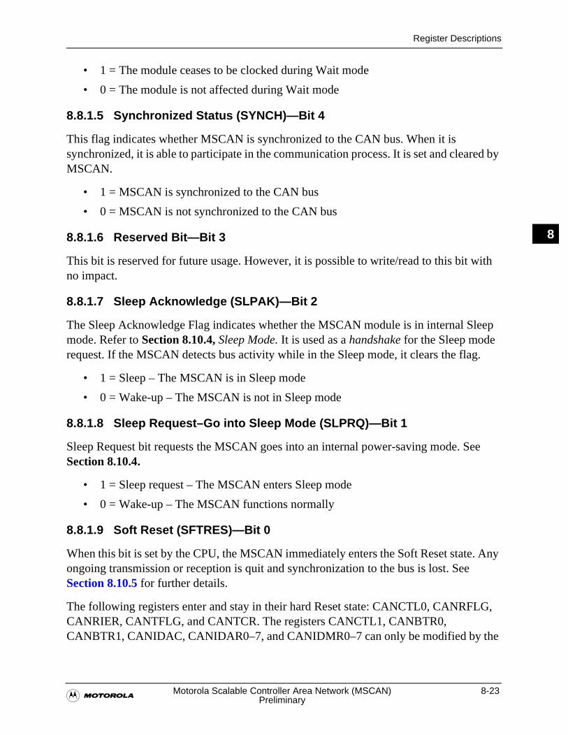
Register Descriptions
�Motorola Scalable Controller Area Network (MSCAN) 8-23
Preliminary
8
• 1 = The module ceases to be clocked during Wait mode
• 0 = The module is not affected during Wait mode
8.8.1.5 Synchronized Status (SYNCH)—Bit 4
This flag indicates whether MSCAN is synchronized to the CAN bus. When it is synchronized, it is able to participate in the communication process. It is set and cleared by MSCAN.
• 1 = MSCAN is synchronized to the CAN bus
• 0 = MSCAN is not synchronized to the CAN bus
8.8.1.6 Reserved Bit—Bit 3
This bit is reserved for future usage. However, it is possible to write/read to this bit with no impact.
8.8.1.7 Sleep Acknowledge (SLPAK)—Bit 2
The Sleep Acknowledge Flag indicates whether the MSCAN module is in internal Sleep mode. Refer to Section 8.10.4, Sleep Mode. It is used as a handshake for the Sleep mode request. If the MSCAN detects bus activity while in the Sleep mode, it clears the flag.
• 1 = Sleep – The MSCAN is in Sleep mode
• 0 = Wake-up – The MSCAN is not in Sleep mode
8.8.1.8 Sleep Request–Go into Sleep Mode (SLPRQ)—Bit 1
Sleep Request bit requests the MSCAN goes into an internal power-saving mode. See Section 8.10.4.
• 1 = Sleep request – The MSCAN enters Sleep mode
• 0 = Wake-up – The MSCAN functions normally
8.8.1.9 Soft Reset (SFTRES)—Bit 0
When this bit is set by the CPU, the MSCAN immediately enters the Soft Reset state. Any ongoing transmission or reception is quit and synchronization to the bus is lost. See Section 8.10.5 for further details.
The following registers enter and stay in their hard Reset state: CANCTL0, CANRFLG, CANRIER, CANTFLG, and CANTCR. The registers CANCTL1, CANBTR0, CANBTR1, CANIDAC, CANIDAR0–7, and CANIDMR0–7 can only be modified by the
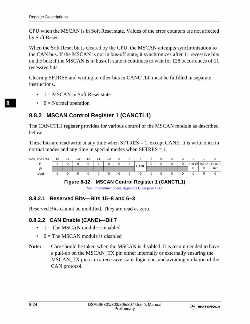
8-24 DSP56F801/803/805/807 User’s Manual�Preliminary
Register Descriptions
8
CPU when the MSCAN is in Soft Reset state. Values of the error counters are not affected by Soft Reset.
When the Soft Reset bit is cleared by the CPU, the MSCAN attempts synchronization to the CAN bus. If the MSCAN is not in bus-off state, it synchronizes after 11 recessive bits on the bus; if the MSCAN is in bus-off state it continues to wait for 128 occurrences of 11 recessive bits.
Clearing SFTRES and writing to other bits in CANCTL0 must be fulfilled in separate instructions.
• 1 = MSCAN in Soft Reset state
• 0 = Normal operation
8.8.2 MSCAN Control Register 1 (CANCTL1)
The CANCTL1 register provides for various control of the MSCAN module as described below.
These bits are read/write at any time when SFTRES = 1, except CANE. It is write once in normal modes and any time in special modes when SFTRES = 1.
8.8.2.1 Reserved Bits—Bits 15–8 and 6–3
Reserved Bits cannot be modified. They are read as zero.
8.8.2.2 CAN Enable (CANE)—Bit 7• 1 = The MSCAN module is enabled
• 0 = The MSCAN module is disabled
Note: Care should be taken when the MSCAN is disabled. It is recommended to have a pull-up on the MSCAN_TX pin either internally or externally ensuring the MSCAN_TX pin is in a recessive state, logic one, and avoiding violation of the CAN protocol.
CAN_BASE+$1 15 14 13 12 11 10 9 8 7 6 5 4 3 2 1 0
R 0 0 0 0 0 0 0 0CANE
0 0 0 0 LOOPB
WUPM
CLKSRCW
reset 0 0 0 0 0 0 0 0 0 0 0 0 0 0 0 0
Figure 8-12. MSCAN Control Register 1 (CANCTL1)See Programmer Sheet, Appendix C, on page C-42
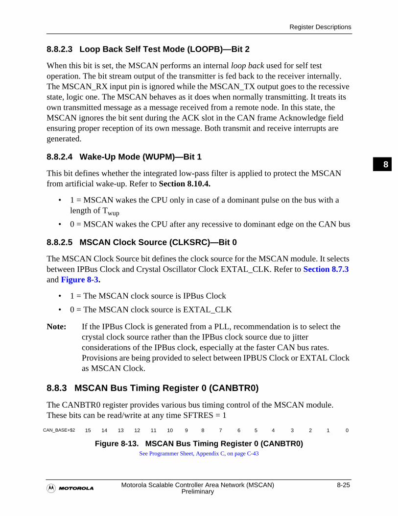
Register Descriptions
�Motorola Scalable Controller Area Network (MSCAN) 8-25
Preliminary
8
8.8.2.3 Loop Back Self Test Mode (LOOPB)—Bit 2
When this bit is set, the MSCAN performs an internal loop back used for self test operation. The bit stream output of the transmitter is fed back to the receiver internally. The MSCAN_RX input pin is ignored while the MSCAN_TX output goes to the recessive state, logic one. The MSCAN behaves as it does when normally transmitting. It treats its own transmitted message as a message received from a remote node. In this state, the MSCAN ignores the bit sent during the ACK slot in the CAN frame Acknowledge field ensuring proper reception of its own message. Both transmit and receive interrupts are generated.
8.8.2.4 Wake-Up Mode (WUPM)—Bit 1
This bit defines whether the integrated low-pass filter is applied to protect the MSCAN from artificial wake-up. Refer to Section 8.10.4.
• 1 = MSCAN wakes the CPU only in case of a dominant pulse on the bus with a length of Twup
• 0 = MSCAN wakes the CPU after any recessive to dominant edge on the CAN bus
8.8.2.5 MSCAN Clock Source (CLKSRC)—Bit 0
The MSCAN Clock Source bit defines the clock source for the MSCAN module. It selects between IPBus Clock and Crystal Oscillator Clock EXTAL_CLK. Refer to Section 8.7.3 and Figure 8-3.
• 1 = The MSCAN clock source is IPBus Clock
• 0 = The MSCAN clock source is EXTAL_CLK
Note: If the IPBus Clock is generated from a PLL, recommendation is to select the crystal clock source rather than the IPBus clock source due to jitter considerations of the IPBus clock, especially at the faster CAN bus rates. Provisions are being provided to select between IPBUS Clock or EXTAL Clock as MSCAN Clock.
8.8.3 MSCAN Bus Timing Register 0 (CANBTR0)
The CANBTR0 register provides various bus timing control of the MSCAN module. These bits can be read/write at any time SFTRES = 1
CAN_BASE+$2 15 14 13 12 11 10 9 8 7 6 5 4 3 2 1 0
Figure 8-13. MSCAN Bus Timing Register 0 (CANBTR0)See Programmer Sheet, Appendix C, on page C-43
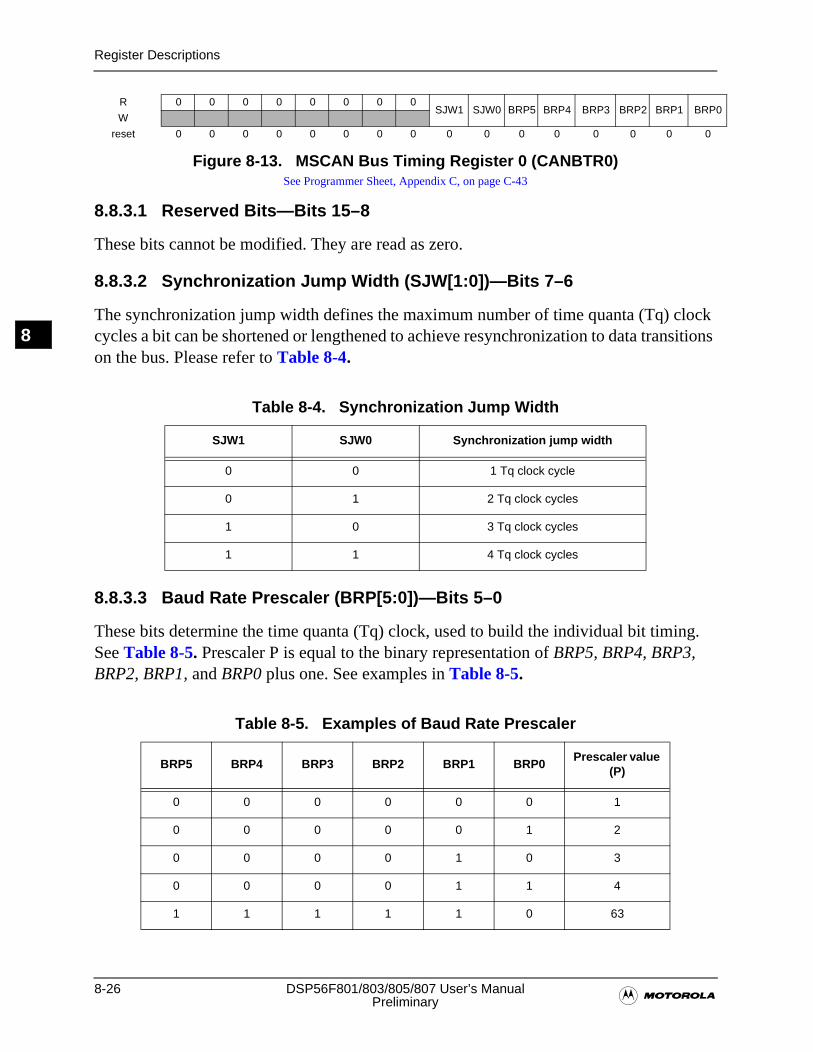
8-26 DSP56F801/803/805/807 User’s Manual�Preliminary
Register Descriptions
8
8.8.3.1 Reserved Bits—Bits 15–8
These bits cannot be modified. They are read as zero.
8.8.3.2 Synchronization Jump Width (SJW[1:0])—Bits 7–6
The synchronization jump width defines the maximum number of time quanta (Tq) clock cycles a bit can be shortened or lengthened to achieve resynchronization to data transitions on the bus. Please refer to Table 8-4.
8.8.3.3 Baud Rate Prescaler (BRP[5:0])—Bits 5–0
These bits determine the time quanta (Tq) clock, used to build the individual bit timing. See Table 8-5. Prescaler P is equal to the binary representation of BRP5, BRP4, BRP3, BRP2, BRP1, and BRP0 plus one. See examples in Table 8-5.
R 0 0 0 0 0 0 0 0SJW1 SJW0 BRP5 BRP4 BRP3 BRP2 BRP1 BRP0
W
reset 0 0 0 0 0 0 0 0 0 0 0 0 0 0 0 0
Table 8-4. Synchronization Jump Width
SJW1 SJW0 Synchronization jump width
0 0 1 Tq clock cycle
0 1 2 Tq clock cycles
1 0 3 Tq clock cycles
1 1 4 Tq clock cycles
Table 8-5. Examples of Baud Rate Prescaler
BRP5 BRP4 BRP3 BRP2 BRP1 BRP0Prescaler value
(P)
0 0 0 0 0 0 1
0 0 0 0 0 1 2
0 0 0 0 1 0 3
0 0 0 0 1 1 4
1 1 1 1 1 0 63
Figure 8-13. MSCAN Bus Timing Register 0 (CANBTR0)See Programmer Sheet, Appendix C, on page C-43
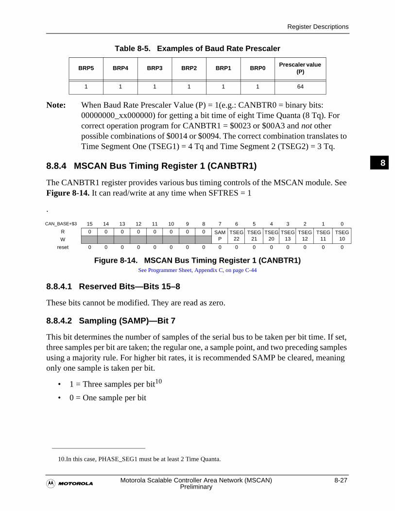
Register Descriptions
�Motorola Scalable Controller Area Network (MSCAN) 8-27
Preliminary
8
Note: When Baud Rate Prescaler Value (P) = 1(e.g.: CANBTR0 = binary bits: 00000000_xx000000) for getting a bit time of eight Time Quanta (8 Tq). For correct operation program for CANBTR1 = $0023 or $00A3 and not other possible combinations of $0014 or $0094. The correct combination translates to Time Segment One (TSEG1) = 4 Tq and Time Segment 2 (TSEG2) = 3 Tq.
8.8.4 MSCAN Bus Timing Register 1 (CANBTR1)
The CANBTR1 register provides various bus timing controls of the MSCAN module. See Figure 8-14. It can read/write at any time when SFTRES = 1
.
8.8.4.1 Reserved Bits—Bits 15–8
These bits cannot be modified. They are read as zero.
8.8.4.2 Sampling (SAMP)—Bit 7
This bit determines the number of samples of the serial bus to be taken per bit time. If set, three samples per bit are taken; the regular one, a sample point, and two preceding samples using a majority rule. For higher bit rates, it is recommended SAMP be cleared, meaning only one sample is taken per bit.
• 1 = Three samples per bit10
• 0 = One sample per bit
1 1 1 1 1 1 64
CAN_BASE+$3 15 14 13 12 11 10 9 8 7 6 5 4 3 2 1 0
R 0 0 0 0 0 0 0 0 SAMP
TSEG22
TSEG21
TSEG20
TSEG13
TSEG12
TSEG11
TSEG10W
reset 0 0 0 0 0 0 0 0 0 0 0 0 0 0 0 0
Figure 8-14. MSCAN Bus Timing Register 1 (CANBTR1)See Programmer Sheet, Appendix C, on page C-44
10.In this case, PHASE_SEG1 must be at least 2 Time Quanta.
Table 8-5. Examples of Baud Rate Prescaler
BRP5 BRP4 BRP3 BRP2 BRP1 BRP0Prescaler value
(P)
8-28 DSP56F801/803/805/807 User’s Manual�Preliminary
Register Descriptions
8
8.8.4.3 Time Segment 2 (TSEG22–TSEG20)—Bits 6–4
Time segments within the bit time fix the number of clock cycles per bit time and the location of the sample point. See Figure 8-10. Time segment two (TSEG2) values are programmable as illustrated in Table 8-6.
8.8.4.4 Time Segment 1 (TSEG13–TSEG10)—Bits 3–0
Time segments within the bit time fix the number of clock cycles per bit time and the location of the sample point. Please refer to Figure 8-10.
Time segment One (TSEG1) values are programmable as shown in Table 8-7.
Table 8-6. Time Segment 2 Values
TSEG22 TSEG21 TSEG20 Time segment 2
0 0 0 1 Tq clock cycle1
1.This setting is not valid. Please refer to Table 8-2. CAN Standard Compliance Bit Time Segment Settings for valid settings.
0 0 1 2 Tq clock cycles
0 1 0 3 Tq clock cycles
0 1 1 4 Tq clock cycles
1 0 0 5 Tq clock cycles
1 0 1 6 Tq clock cycles
1 1 0 7 Tq clock cycles
1 1 1 8 Tq clock cycles
Table 8-7. Time Segment 1 Values
TSEG13 TSEG12 TSEG11 TSEG10 Time segment 1
0 0 0 0 1 Tq clock cycle1
0 0 0 1 2 Tq clock cycles1
0 0 1 0 3 Tq clock cycles1
0 0 1 1 4 Tq clock cycles
0 1 0 0 5 Tq clock cycles
0 1 0 1 6 Tq clock cycles
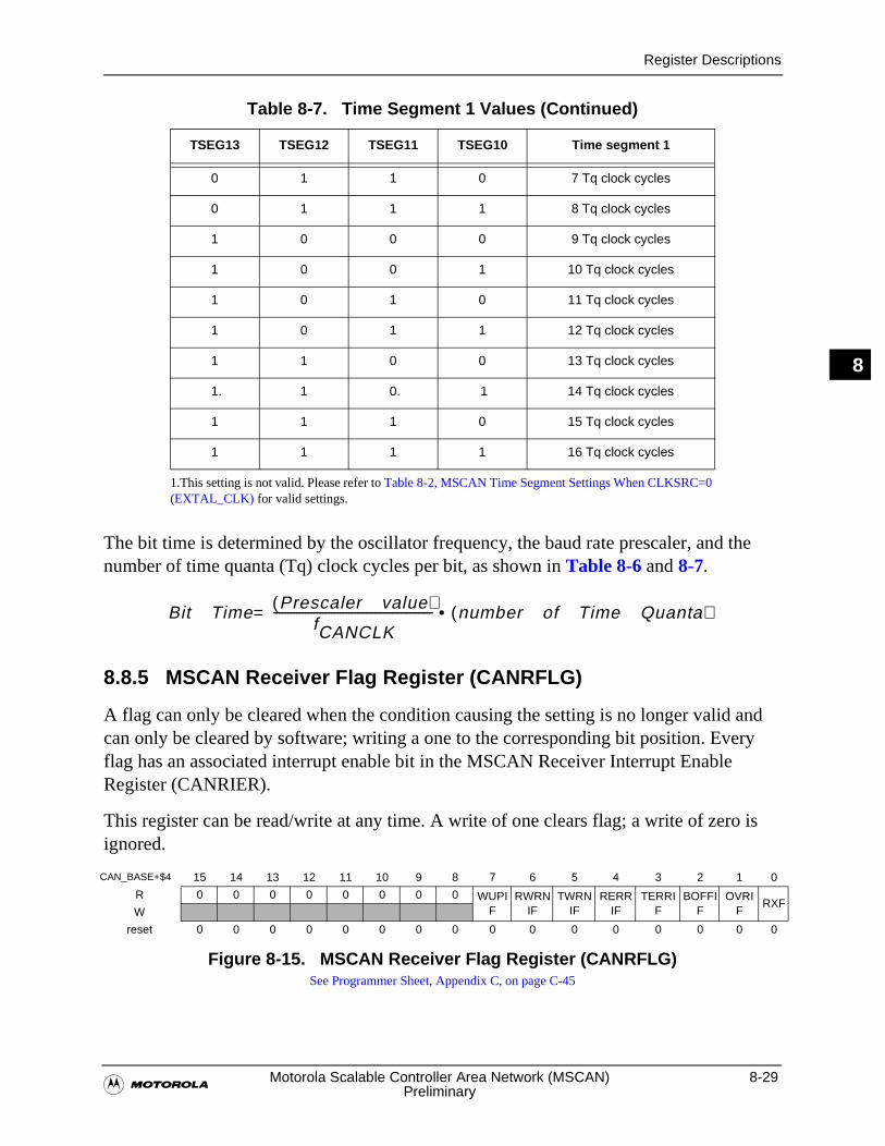
Register Descriptions
�Motorola Scalable Controller Area Network (MSCAN) 8-29
Preliminary
8
The bit time is determined by the oscillator frequency, the baud rate prescaler, and the number of time quanta (Tq) clock cycles per bit, as shown in Table 8-6 and 8-7.
8.8.5 MSCAN Receiver Flag Register (CANRFLG)
A flag can only be cleared when the condition causing the setting is no longer valid and can only be cleared by software; writing a one to the corresponding bit position. Every flag has an associated interrupt enable bit in the MSCAN Receiver Interrupt Enable Register (CANRIER).
This register can be read/write at any time. A write of one clears flag; a write of zero is ignored.
0 1 1 0 7 Tq clock cycles
0 1 1 1 8 Tq clock cycles
1 0 0 0 9 Tq clock cycles
1 0 0 1 10 Tq clock cycles
1 0 1 0 11 Tq clock cycles
1 0 1 1 12 Tq clock cycles
1 1 0 0 13 Tq clock cycles
1. 1 0. 1 14 Tq clock cycles
1 1 1 0 15 Tq clock cycles
1 1 1 1 16 Tq clock cycles
1.This setting is not valid. Please refer to Table 8-2, MSCAN Time Segment Settings When CLKSRC=0 (EXTAL_CLK) for valid settings.
CAN_BASE+$4 15 14 13 12 11 10 9 8 7 6 5 4 3 2 1 0
R 0 0 0 0 0 0 0 0 WUPIF
RWRNIF
TWRNIF
RERRIF
TERRIF
BOFFIF
OVRIF
RXFW
reset 0 0 0 0 0 0 0 0 0 0 0 0 0 0 0 0
Figure 8-15. MSCAN Receiver Flag Register (CANRFLG)See Programmer Sheet, Appendix C, on page C-45
Table 8-7. Time Segment 1 Values (Continued)
TSEG13 TSEG12 TSEG11 TSEG10 Time segment 1
Bit Time Prescaler valueÞ( )fCANCLK
------------------------------------------------------- number of Time QuantaÞ Þ Þ( )•=Þ
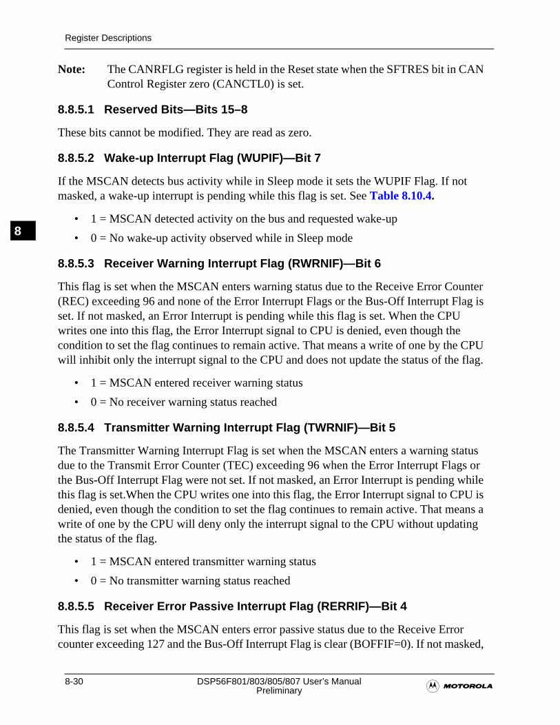
8-30 DSP56F801/803/805/807 User’s Manual�Preliminary
Register Descriptions
8
Note: The CANRFLG register is held in the Reset state when the SFTRES bit in CAN Control Register zero (CANCTL0) is set.
8.8.5.1 Reserved Bits—Bits 15–8
These bits cannot be modified. They are read as zero.
8.8.5.2 Wake-up Interrupt Flag (WUPIF)—Bit 7
If the MSCAN detects bus activity while in Sleep mode it sets the WUPIF Flag. If not masked, a wake-up interrupt is pending while this flag is set. See Table 8.10.4.
• 1 = MSCAN detected activity on the bus and requested wake-up
• 0 = No wake-up activity observed while in Sleep mode
8.8.5.3 Receiver Warning Interrupt Flag (RWRNIF)—Bit 6
This flag is set when the MSCAN enters warning status due to the Receive Error Counter (REC) exceeding 96 and none of the Error Interrupt Flags or the Bus-Off Interrupt Flag is set. If not masked, an Error Interrupt is pending while this flag is set. When the CPU writes one into this flag, the Error Interrupt signal to CPU is denied, even though the condition to set the flag continues to remain active. That means a write of one by the CPU will inhibit only the interrupt signal to the CPU and does not update the status of the flag.
• 1 = MSCAN entered receiver warning status
• 0 = No receiver warning status reached
8.8.5.4 Transmitter Warning Interrupt Flag (TWRNIF)—Bit 5
The Transmitter Warning Interrupt Flag is set when the MSCAN enters a warning status due to the Transmit Error Counter (TEC) exceeding 96 when the Error Interrupt Flags or the Bus-Off Interrupt Flag were not set. If not masked, an Error Interrupt is pending while this flag is set.When the CPU writes one into this flag, the Error Interrupt signal to CPU is denied, even though the condition to set the flag continues to remain active. That means a write of one by the CPU will deny only the interrupt signal to the CPU without updating the status of the flag.
• 1 = MSCAN entered transmitter warning status
• 0 = No transmitter warning status reached
8.8.5.5 Receiver Error Passive Interrupt Flag (RERRIF)—Bit 4
This flag is set when the MSCAN enters error passive status due to the Receive Error counter exceeding 127 and the Bus-Off Interrupt Flag is clear (BOFFIF=0). If not masked,
Register Descriptions
�Motorola Scalable Controller Area Network (MSCAN) 8-31
Preliminary
8
an Error Interrupt is pending while this flag is set. When the CPU writes one into this flag, the Error Interrupt signal to CPU is denied, even though the condition to set the flag continues to remain active. That means a write of one by the CPU will deny only the Interrupt signal to the CPU without updating the status of the flag.
• 1 = MSCAN entered receiver error passive status
• 0 = No receiver error passive status reached
8.8.5.6 Transmitter Error Passive Interrupt Flag (TERRIF)—Bit 3
This flag is set when the MSCAN enters error passive status due to the Transmit Error counter exceeding 127 and the Bus-Off Interrupt Flag is clear (BOFFIF = 0). If not masked, an Error Interrupt is pending while this flag is set.When the CPU writes one into this flag, the Error Interrupt signal to CPU is denied, even though the condition to set the flag continues to remain active. That means a write of one by the CPU will deny only the Interrupt signal to the CPU without updating the status of the flag.
• 1 = MSCAN entered transmitter error passive status
• 0 = No transmitter error passive status reached
8.8.5.7 Bus-Off Interrupt Flag (BOFFIF)—Bit 2
The Bus-off Interrupt Flag is set when the MSCAN enters bus-off status, resulting in the Transmit Error counter exceeding 255. It cannot be cleared before the MSCAN has monitored 128 times 11 consecutive recessive bits on the bus. If not masked, an Error Interrupt is pending while this flag is set. When the CPU writes one into this flag, the Error Interrupt signal to CPU is denied, even though the condition to set the flag continues to remain active. That means a write of one by the CPU will deny only the interrupt signal to the CPU without updating the status of the flag.
• 1 = MSCAN entered into bus-off status
• 0 = No bus-off status reached
8.8.5.8 Overrun Interrupt Flag (OVRIF)—Bit 1
This flag is set when a data overrun condition occurs. If not masked, an Error Interrupt is pending if this flag is set.
• 1 = A data overrun detected
• 0 = No data overrun condition
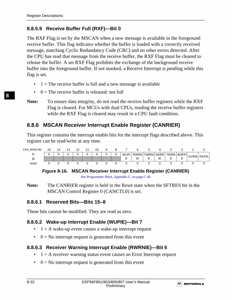
8-32 DSP56F801/803/805/807 User’s Manual�Preliminary
Register Descriptions
8
8.8.5.9 Receive Buffer Full (RXF)—Bit 0
The RXF Flag is set by the MSCAN when a new message is available in the foreground receive buffer. This flag indicates whether the buffer is loaded with a correctly received message, matching Cyclic Redundancy Code (CRC) and no other errors detected. After the CPU has read that message from the receive buffer, the RXF Flag must be cleared to release the buffer. A set RXF Flag prohibits the exchange of the background receive buffer into the foreground buffer. If not masked, a Receive Interrupt is pending while this flag is set.
• 1 = The receive buffer is full and a new message is available
• 0 = The receive buffer is released: not full
Note: To ensure data integrity, do not read the receive buffer registers while the RXF Flag is cleared. For MCUs with dual CPUs, reading the receive buffer registers while the RXF Flag is cleared may result in a CPU fault condition.
8.8.6 MSCAN Receiver Interrupt Enable Register (CANRIER)
This register contains the interrupt enable bits for the interrupt flags described above. This register can be read/write at any time.
Note: The CANRIER register is held in the Reset state when the SFTRES bit in the MSCAN Control Register 0 (CANCTL0) is set.
8.8.6.1 Reserved Bits—Bits 15–8
These bits cannot be modified. They are read as zero.
8.8.6.2 Wake-up Interrupt Enable (WUPIE)—Bit 7• 1 = A wake-up event causes a wake-up interrupt request
• 0 = No interrupt request is generated from this event
8.8.6.3 Receiver Warning Interrupt Enable (RWRNIE)—Bit 6• 1 = A receiver warning status event causes an Error Interrupt request
• 0 = No interrupt request is generated from this event
CAN_BASE+$5 15 14 13 12 11 10 9 8 7 6 5 4 3 2 1 0
R 0 0 0 0 0 0 0 0 WUPIE
RWRNIE
TWRNIE
RERRIE
TERRIE
BOFFIE
OVRIE RXFIEW
reset 0 0 0 0 0 0 0 0 0 0 0 0 0 0 0 0
Figure 8-16. MSCAN Receiver Interrupt Enable Register (CANRIER)See Programmer Sheet, Appendix C, on page C-46
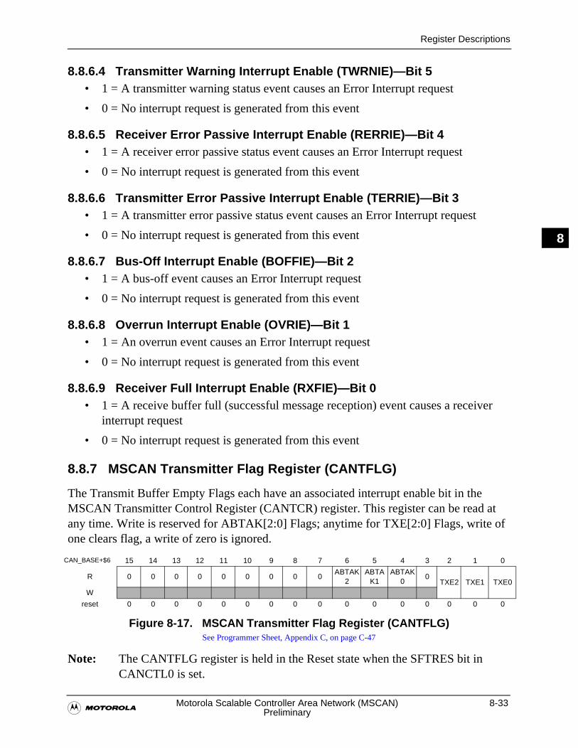
Register Descriptions
�Motorola Scalable Controller Area Network (MSCAN) 8-33
Preliminary
8
8.8.6.4 Transmitter Warning Interrupt Enable (TWRNIE)—Bit 5• 1 = A transmitter warning status event causes an Error Interrupt request
• 0 = No interrupt request is generated from this event
8.8.6.5 Receiver Error Passive Interrupt Enable (RERRIE)—Bit 4• 1 = A receiver error passive status event causes an Error Interrupt request
• 0 = No interrupt request is generated from this event
8.8.6.6 Transmitter Error Passive Interrupt Enable (TERRIE)—Bit 3• 1 = A transmitter error passive status event causes an Error Interrupt request
• 0 = No interrupt request is generated from this event
8.8.6.7 Bus-Off Interrupt Enable (BOFFIE)—Bit 2• 1 = A bus-off event causes an Error Interrupt request
• 0 = No interrupt request is generated from this event
8.8.6.8 Overrun Interrupt Enable (OVRIE)—Bit 1• 1 = An overrun event causes an Error Interrupt request
• 0 = No interrupt request is generated from this event
8.8.6.9 Receiver Full Interrupt Enable (RXFIE)—Bit 0• 1 = A receive buffer full (successful message reception) event causes a receiver
interrupt request
• 0 = No interrupt request is generated from this event
8.8.7 MSCAN Transmitter Flag Register (CANTFLG)
The Transmit Buffer Empty Flags each have an associated interrupt enable bit in the MSCAN Transmitter Control Register (CANTCR) register. This register can be read at any time. Write is reserved for ABTAK[2:0] Flags; anytime for TXE[2:0] Flags, write of one clears flag, a write of zero is ignored.
Note: The CANTFLG register is held in the Reset state when the SFTRES bit in CANCTL0 is set.
CAN_BASE+$6 15 14 13 12 11 10 9 8 7 6 5 4 3 2 1 0
R 0 0 0 0 0 0 0 0 0ABTAK
2ABTA
K1ABTAK
00
TXE2 TXE1 TXE0W
reset 0 0 0 0 0 0 0 0 0 0 0 0 0 0 0 0
Figure 8-17. MSCAN Transmitter Flag Register (CANTFLG)See Programmer Sheet, Appendix C, on page C-47
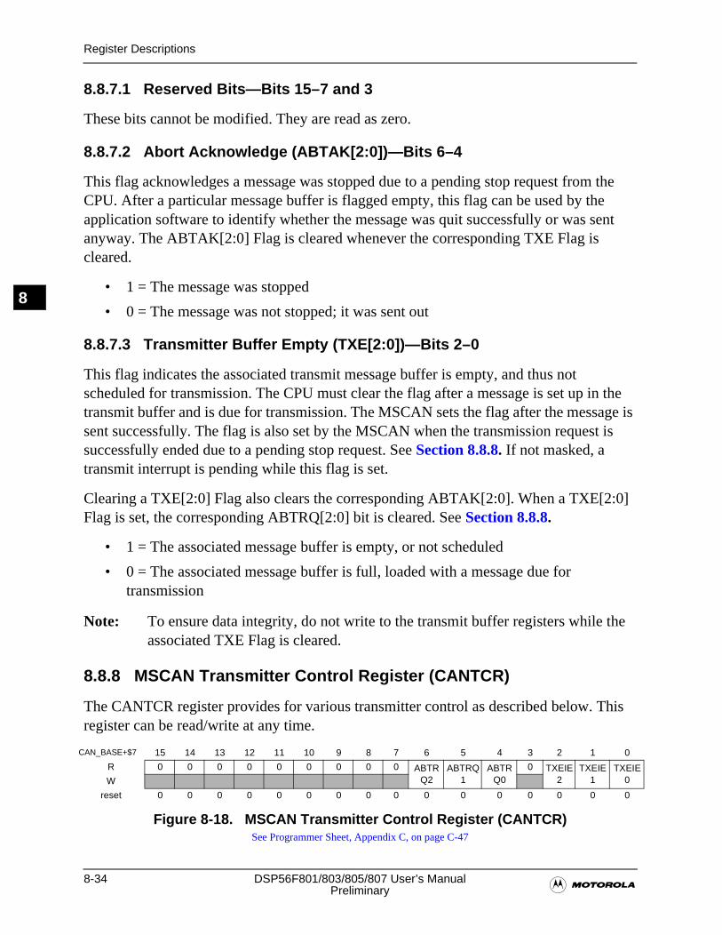
8-34 DSP56F801/803/805/807 User’s Manual�Preliminary
Register Descriptions
8
8.8.7.1 Reserved Bits—Bits 15–7 and 3
These bits cannot be modified. They are read as zero.
8.8.7.2 Abort Acknowledge (ABTAK[2:0])—Bits 6–4
This flag acknowledges a message was stopped due to a pending stop request from the CPU. After a particular message buffer is flagged empty, this flag can be used by the application software to identify whether the message was quit successfully or was sent anyway. The ABTAK[2:0] Flag is cleared whenever the corresponding TXE Flag is cleared.
• 1 = The message was stopped
• 0 = The message was not stopped; it was sent out
8.8.7.3 Transmitter Buffer Empty (TXE[2:0])—Bits 2–0
This flag indicates the associated transmit message buffer is empty, and thus not scheduled for transmission. The CPU must clear the flag after a message is set up in the transmit buffer and is due for transmission. The MSCAN sets the flag after the message is sent successfully. The flag is also set by the MSCAN when the transmission request is successfully ended due to a pending stop request. See Section 8.8.8. If not masked, a transmit interrupt is pending while this flag is set.
Clearing a TXE[2:0] Flag also clears the corresponding ABTAK[2:0]. When a TXE[2:0] Flag is set, the corresponding ABTRQ[2:0] bit is cleared. See Section 8.8.8.
• 1 = The associated message buffer is empty, or not scheduled
• 0 = The associated message buffer is full, loaded with a message due for transmission
Note: To ensure data integrity, do not write to the transmit buffer registers while the associated TXE Flag is cleared.
8.8.8 MSCAN Transmitter Control Register (CANTCR)
The CANTCR register provides for various transmitter control as described below. This register can be read/write at any time.
CAN_BASE+$7 15 14 13 12 11 10 9 8 7 6 5 4 3 2 1 0
R 0 0 0 0 0 0 0 0 0 ABTRQ2
ABTRQ1
ABTRQ0
0 TXEIE2
TXEIE1
TXEIE0W
reset 0 0 0 0 0 0 0 0 0 0 0 0 0 0 0 0
Figure 8-18. MSCAN Transmitter Control Register (CANTCR)See Programmer Sheet, Appendix C, on page C-47
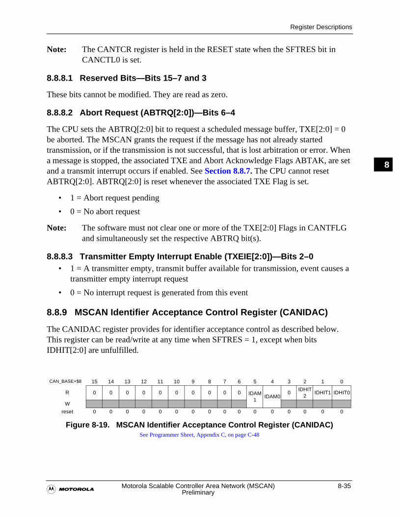
Register Descriptions
�Motorola Scalable Controller Area Network (MSCAN) 8-35
Preliminary
8
Note: The CANTCR register is held in the RESET state when the SFTRES bit in CANCTL0 is set.
8.8.8.1 Reserved Bits—Bits 15–7 and 3
These bits cannot be modified. They are read as zero.
8.8.8.2 Abort Request (ABTRQ[2:0])—Bits 6–4
The CPU sets the ABTRQ[2:0] bit to request a scheduled message buffer, TXE[2:0] = 0 be aborted. The MSCAN grants the request if the message has not already started transmission, or if the transmission is not successful, that is lost arbitration or error. When a message is stopped, the associated TXE and Abort Acknowledge Flags ABTAK, are set and a transmit interrupt occurs if enabled. See Section 8.8.7. The CPU cannot reset ABTRQ[2:0]. ABTRQ[2:0] is reset whenever the associated TXE Flag is set.
• 1 = Abort request pending
• 0 = No abort request
Note: The software must not clear one or more of the TXE[2:0] Flags in CANTFLG and simultaneously set the respective ABTRQ bit(s).
8.8.8.3 Transmitter Empty Interrupt Enable (TXEIE[2:0])—Bits 2–0• 1 = A transmitter empty, transmit buffer available for transmission, event causes a
transmitter empty interrupt request
• 0 = No interrupt request is generated from this event
8.8.9 MSCAN Identifier Acceptance Control Register (CANIDAC)
The CANIDAC register provides for identifier acceptance control as described below. This register can be read/write at any time when SFTRES = 1, except when bits IDHIT[2:0] are unfulfilled.
CAN_BASE+$8 15 14 13 12 11 10 9 8 7 6 5 4 3 2 1 0
R 0 0 0 0 0 0 0 0 0 0 IDAM1
IDAM00
IDHIT2
IDHIT1 IDHIT0
W
reset 0 0 0 0 0 0 0 0 0 0 0 0 0 0 0 0
Figure 8-19. MSCAN Identifier Acceptance Control Register (CANIDAC)See Programmer Sheet, Appendix C, on page C-48
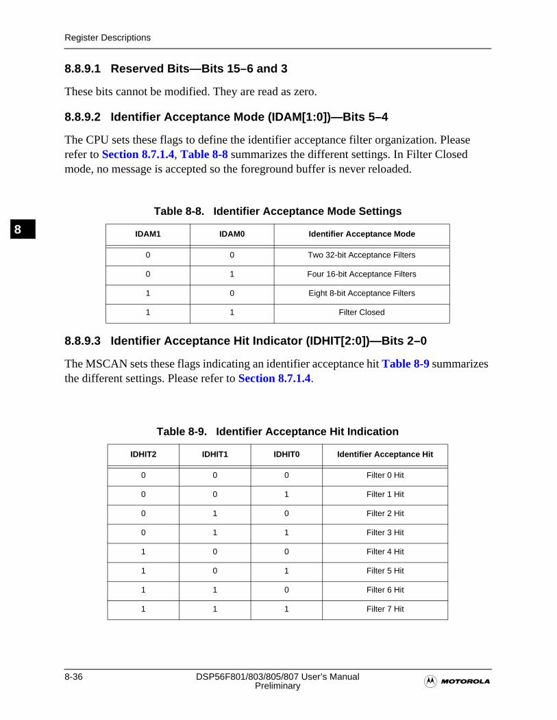
8-36 DSP56F801/803/805/807 User’s Manual�Preliminary
Register Descriptions
8
8.8.9.1 Reserved Bits—Bits 15–6 and 3
These bits cannot be modified. They are read as zero.
8.8.9.2 Identifier Acceptance Mode (IDAM[1:0])—Bits 5–4
The CPU sets these flags to define the identifier acceptance filter organization. Please refer to Section 8.7.1.4, Table 8-8 summarizes the different settings. In Filter Closed mode, no message is accepted so the foreground buffer is never reloaded.
8.8.9.3 Identifier Acceptance Hit Indicator (IDHIT[2:0])—Bits 2–0
The MSCAN sets these flags indicating an identifier acceptance hit Table 8-9 summarizes the different settings. Please refer to Section 8.7.1.4.
Table 8-8. Identifier Acceptance Mode Settings
IDAM1 IDAM0 Identifier Acceptance Mode
0 0 Two 32-bit Acceptance Filters
0 1 Four 16-bit Acceptance Filters
1 0 Eight 8-bit Acceptance Filters
1 1 Filter Closed
Table 8-9. Identifier Acceptance Hit Indication
IDHIT2 IDHIT1 IDHIT0 Identifier Acceptance Hit
0 0 0 Filter 0 Hit
0 0 1 Filter 1 Hit
0 1 0 Filter 2 Hit
0 1 1 Filter 3 Hit
1 0 0 Filter 4 Hit
1 0 1 Filter 5 Hit
1 1 0 Filter 6 Hit
1 1 1 Filter 7 Hit
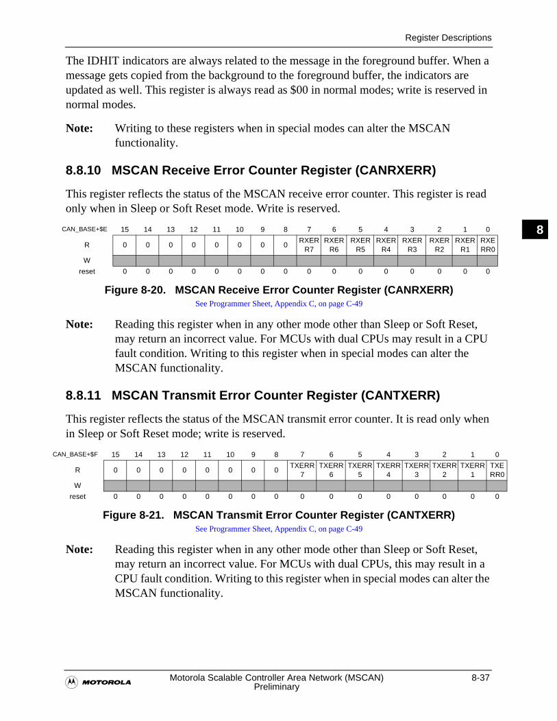
Register Descriptions
�Motorola Scalable Controller Area Network (MSCAN) 8-37
Preliminary
8
The IDHIT indicators are always related to the message in the foreground buffer. When a message gets copied from the background to the foreground buffer, the indicators are updated as well. This register is always read as $00 in normal modes; write is reserved in normal modes.
Note: Writing to these registers when in special modes can alter the MSCAN functionality.
8.8.10 MSCAN Receive Error Counter Register (CANRXERR)
This register reflects the status of the MSCAN receive error counter. This register is read only when in Sleep or Soft Reset mode. Write is reserved.
Note: Reading this register when in any other mode other than Sleep or Soft Reset, may return an incorrect value. For MCUs with dual CPUs may result in a CPU fault condition. Writing to this register when in special modes can alter the MSCAN functionality.
8.8.11 MSCAN Transmit Error Counter Register (CANTXERR)
This register reflects the status of the MSCAN transmit error counter. It is read only when in Sleep or Soft Reset mode; write is reserved.
Note: Reading this register when in any other mode other than Sleep or Soft Reset, may return an incorrect value. For MCUs with dual CPUs, this may result in a CPU fault condition. Writing to this register when in special modes can alter the MSCAN functionality.
CAN_BASE+$E 15 14 13 12 11 10 9 8 7 6 5 4 3 2 1 0
R 0 0 0 0 0 0 0 0RXER
R7RXER
R6RXER
R5RXER
R4RXER
R3RXER
R2RXER
R1RXERR0
W
reset 0 0 0 0 0 0 0 0 0 0 0 0 0 0 0 0
Figure 8-20. MSCAN Receive Error Counter Register (CANRXERR)See Programmer Sheet, Appendix C, on page C-49
CAN_BASE+$F 15 14 13 12 11 10 9 8 7 6 5 4 3 2 1 0
R 0 0 0 0 0 0 0 0TXERR
7TXERR
6TXERR
5TXERR
4TXERR
3TXERR
2TXERR
1TXERR0
W
reset 0 0 0 0 0 0 0 0 0 0 0 0 0 0 0 0
Figure 8-21. MSCAN Transmit Error Counter Register (CANTXERR)See Programmer Sheet, Appendix C, on page C-49
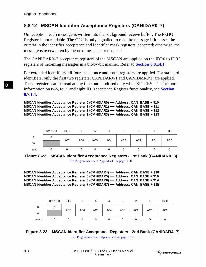
8-38 DSP56F801/803/805/807 User’s Manual�Preliminary
Register Descriptions
8
8.8.12 MSCAN Identifier Acceptance Registers (CANIDAR0–7)
On reception, each message is written into the background receive buffer. The RxBG Register is not readable. The CPU is only signalled to read the message if it passes the criteria in the identifier acceptance and identifier mask registers, accepted; otherwise, the message is overwritten by the next message, or dropped.
The CANIDAR0–7 acceptance registers of the MSCAN are applied on the IDR0 to IDR3 registers of incoming messages in a bit-by-bit manner. Refer to Section 8.8.14.1.
For extended identifiers, all four acceptance and mask registers are applied. For standard identifiers, only the first two registers, CANIDAR0/1 and CANIDMR0/1, are applied. These registers can be read at any time and modified only when SFTRES = 1. For more information on two, four, and eight ID Acceptance Register functionality, see Section 8.7.1.4.
MSCAN Identifier Acceptance Register 0 (CANIDAR0) — Address: CAN_BASE + $10MSCAN Identifier Acceptance Register 1 (CANIDAR1) — Address: CAN_BASE + $11MSCAN Identifier Acceptance Register 2 (CANIDAR2) — Address: CAN_BASE + $12MSCAN Identifier Acceptance Register 3 (CANIDAR3) — Address: CAN_BASE + $13
MSCAN Identifier Acceptance Register 4 (CANIDAR4) — Address: CAN_BASE + $18MSCAN Identifier Acceptance Register 5 (CANIDAR5) — Address: CAN_BASE + $19MSCAN Identifier Acceptance Register 6 (CANIDAR6) — Address: CAN_BASE + $1AMSCAN Identifier Acceptance Register 7 (CANIDAR7) — Address: CAN_BASE + $1B
Figure 8-23. MSCAN Identifier Acceptance Registers - 2nd Bank (CANIDAR4–7)See Programmer Sheet, Appendix C, on page C-51
Bits 15-8 Bit 7 6 5 4 3 2 1 Bit 0
R 0AC7 AC6 AC5 AC4 AC3 AC2 AC1 AC0
W
reset 0 0 0 0 0 0 0 0 0
Figure 8-22. MSCAN Identifier Acceptance Registers - 1st Bank (CANIDAR0–3)See Programmer Sheet, Appendix C, on page C-50
Bits 15-8 Bit 7 6 5 4 3 2 1 Bit 0
R 0AC7 AC6 AC5 AC4 AC3 AC2 AC1 AC0
W
reset 0 0 0 0 0 0 0 0 0
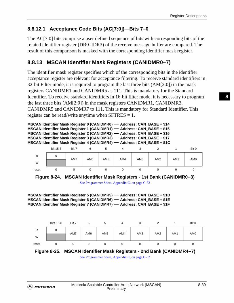
Register Descriptions
�Motorola Scalable Controller Area Network (MSCAN) 8-39
Preliminary
8
8.8.12.1 Acceptance Code Bits (AC[7:0])—Bits 7–0
The AC[7:0] bits comprise a user defined sequence of bits with corresponding bits of the related identifier register (DR0–IDR3) of the receive message buffer are compared. The result of this comparison is masked with the corresponding identifier mask register.
8.8.13 MSCAN Identifier Mask Registers (CANIDMR0–7)
The identifier mask register specifies which of the corresponding bits in the identifier acceptance register are relevant for acceptance filtering. To receive standard identifiers in 32-bit Filter mode, it is required to program the last three bits (AM[2:0]) in the mask registers CANIDMR1 and CANIDMR5 as 111. This is mandatory for the Standard Identifier. To receive standard identifiers in 16-bit filter mode, it is necessary to program the last three bits (AM[2:0]) in the mask registers CANIDMR1, CANIDMR3, CANIDMR5 and CANIDMR7 to 111. This is mandatory for Standard Identifier. This register can be read/write anytime when SFTRES = 1.
MSCAN Identifier Mask Register 0 (CANIDMR0) — Address: CAN_BASE + $14MSCAN Identifier Mask Register 1 (CANIDMR1) — Address: CAN_BASE + $15MSCAN Identifier Mask Register 2 (CANIDMR2) — Address: CAN_BASE + $16MSCAN Identifier Mask Register 3 (CANIDMR3) — Address: CAN_BASE + $17MSCAN Identifier Mask Register 4 (CANIDMR4) — Address: CAN_BASE + $1C
MSCAN Identifier Mask Register 5 (CANIDMR5) — Address: CAN_BASE + $1DMSCAN Identifier Mask Register 6 (CANIDMR6) — Address: CAN_BASE + $1EMSCAN Identifier Mask Register 7 (CANIDMR7) — Address: CAN_BASE + $1F
Bit 15-8 Bit 7 6 5 4 3 2 1 Bit 0
R 0AM7 AM6 AM5 AM4 AM3 AM2 AM1 AM0
W
reset 0 0 0 0 0 0 0 0 0
Figure 8-24. MSCAN Identifier Mask Registers - 1st Bank (CANIDMR0–3)See Programmer Sheet, Appendix C, on page C-52
Bits 15-8 Bit 7 6 5 4 3 2 1 Bit 0
R 0AM7 AM6 AM5 AM4 AM3 AM2 AM1 AM0
W
reset 0 0 0 0 0 0 0 0 0
Figure 8-25. MSCAN Identifier Mask Registers - 2nd Bank (CANIDMR4–7)See Programmer Sheet, Appendix C, on page C-52
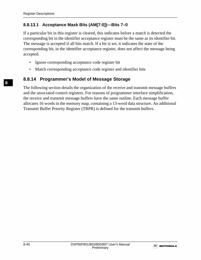
8-40 DSP56F801/803/805/807 User’s Manual�Preliminary
Register Descriptions
8
8.8.13.1 Acceptance Mask Bits (AM[7:0])—Bits 7–0
If a particular bit in this register is cleared, this indicates before a match is detected the corresponding bit in the identifier acceptance register must be the same as its identifier bit. The message is accepted if all bits match. If a bit is set, it indicates the state of the corresponding bit, in the identifier acceptance register, does not affect the message being accepted.
• Ignore corresponding acceptance code register bit
• Match corresponding acceptance code register and identifier bits
8.8.14 Programmer’s Model of Message Storage
The following section details the organization of the receive and transmit message buffers and the associated control registers. For reasons of programmer interface simplification, the receive and transmit message buffers have the same outline. Each message buffer allocates 16 words in the memory map, containing a 13-word data structure. An additional Transmit Buffer Priority Register (TBPR) is defined for the transmit buffers.
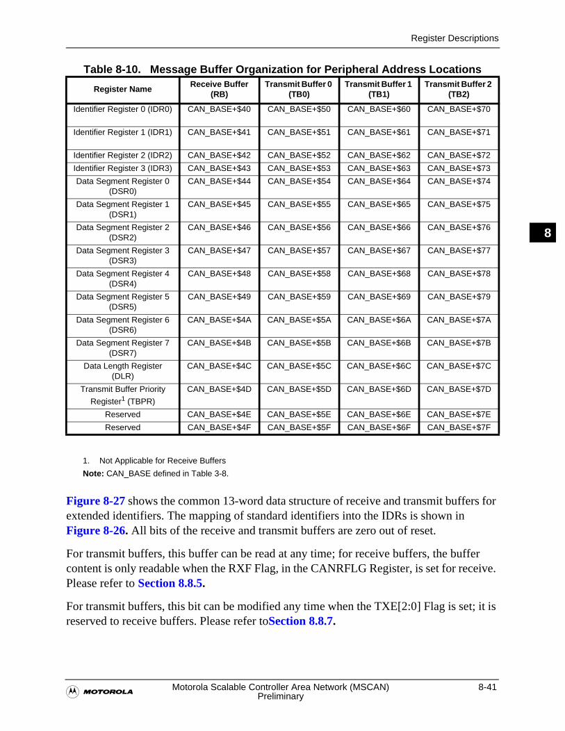
Register Descriptions
�Motorola Scalable Controller Area Network (MSCAN) 8-41
Preliminary
8
Table 8-10. Message Buffer Organization for Peripheral Address Locations
Figure 8-27 shows the common 13-word data structure of receive and transmit buffers for extended identifiers. The mapping of standard identifiers into the IDRs is shown in Figure 8-26. All bits of the receive and transmit buffers are zero out of reset.
For transmit buffers, this buffer can be read at any time; for receive buffers, the buffer content is only readable when the RXF Flag, in the CANRFLG Register, is set for receive. Please refer to Section 8.8.5.
For transmit buffers, this bit can be modified any time when the TXE[2:0] Flag is set; it is reserved to receive buffers. Please refer toSection 8.8.7.
Register NameReceive Buffer
(RB)Transmit Buffer 0
(TB0)Transmit Buffer 1
(TB1)Transmit Buffer 2
(TB2)
Identifier Register 0 (IDR0) CAN_BASE+$40 CAN_BASE+$50 CAN_BASE+$60 CAN_BASE+$70
Identifier Register 1 (IDR1) CAN_BASE+$41 CAN_BASE+$51 CAN_BASE+$61 CAN_BASE+$71
Identifier Register 2 (IDR2) CAN_BASE+$42 CAN_BASE+$52 CAN_BASE+$62 CAN_BASE+$72
Identifier Register 3 (IDR3) CAN_BASE+$43 CAN_BASE+$53 CAN_BASE+$63 CAN_BASE+$73
Data Segment Register 0 (DSR0)
CAN_BASE+$44 CAN_BASE+$54 CAN_BASE+$64 CAN_BASE+$74
Data Segment Register 1 (DSR1)
CAN_BASE+$45 CAN_BASE+$55 CAN_BASE+$65 CAN_BASE+$75
Data Segment Register 2 (DSR2)
CAN_BASE+$46 CAN_BASE+$56 CAN_BASE+$66 CAN_BASE+$76
Data Segment Register 3 (DSR3)
CAN_BASE+$47 CAN_BASE+$57 CAN_BASE+$67 CAN_BASE+$77
Data Segment Register 4 (DSR4)
CAN_BASE+$48 CAN_BASE+$58 CAN_BASE+$68 CAN_BASE+$78
Data Segment Register 5 (DSR5)
CAN_BASE+$49 CAN_BASE+$59 CAN_BASE+$69 CAN_BASE+$79
Data Segment Register 6 (DSR6)
CAN_BASE+$4A CAN_BASE+$5A CAN_BASE+$6A CAN_BASE+$7A
Data Segment Register 7 (DSR7)
CAN_BASE+$4B CAN_BASE+$5B CAN_BASE+$6B CAN_BASE+$7B
Data Length Register (DLR)
CAN_BASE+$4C CAN_BASE+$5C CAN_BASE+$6C CAN_BASE+$7C
Transmit Buffer Priority
Register1 (TBPR)
1. Not Applicable for Receive Buffers
Note: CAN_BASE defined in Table 3-8.
CAN_BASE+$4D CAN_BASE+$5D CAN_BASE+$6D CAN_BASE+$7D
Reserved CAN_BASE+$4E CAN_BASE+$5E CAN_BASE+$6E CAN_BASE+$7E
Reserved CAN_BASE+$4F CAN_BASE+$5F CAN_BASE+$6F CAN_BASE+$7F
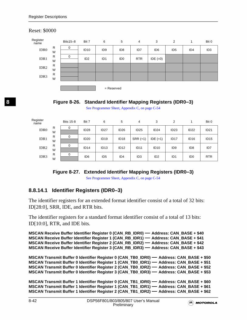
8-42 DSP56F801/803/805/807 User’s Manual�Preliminary
Register Descriptions
8
Reset: $0000
Figure 8-26. Standard Identifier Mapping Registers (IDR0–3)See Programmer Sheet, Appendix C, on page C-54
Figure 8-27. Extended Identifier Mapping Registers (IDR0–3)See Programmer Sheet, Appendix C, on page C-54
8.8.14.1 Identifier Registers (IDR0–3)
The identifier registers for an extended format identifier consist of a total of 32 bits: ID[28:0], SRR, IDE, and RTR bits.
The identifier registers for a standard format identifier consist of a total of 13 bits: ID[10:0], RTR, and IDE bits.
MSCAN Receive Buffer Identifier Register 0 (CAN_RB_IDR0) — Address: CAN_BASE + $40MSCAN Receive Buffer Identifier Register 1 (CAN_RB_IDR1) — Address: CAN_BASE + $41MSCAN Receive Buffer Identifier Register 2 (CAN_RB_IDR2) — Address: CAN_BASE + $42MSCAN Receive Buffer Identifier Register 3 (CAN_RB_IDR3) — Address: CAN_BASE + $43
MSCAN Transmit Buffer 0 Identifier Register 0 (CAN_TB0_IDR0) — Address: CAN_BASE + $50MSCAN Transmit Buffer 0 Identifier Register 1 (CAN_TB0_IDR1) — Address: CAN_BASE + $51MSCAN Transmit Buffer 0 Identifier Register 2 (CAN_TB0_IDR2) — Address: CAN_BASE + $52MSCAN Transmit Buffer 0 Identifier Register 3 (CAN_TB0_IDR3) — Address: CAN_BASE + $53
MSCAN Transmit Buffer 1 Identifier Register 0 (CAN_TB1_IDR0) — Address: CAN_BASE + $60MSCAN Transmit Buffer 1 Identifier Register 1 (CAN_TB1_IDR1) — Address: CAN_BASE + $61MSCAN Transmit Buffer 1 Identifier Register 2 (CAN_TB1_IDR2) — Address: CAN_BASE + $62
Register name Bits15–8 Bit 7 6 5 4 3 2 1 Bit 0
IDR0R 0
ID10 ID9 ID8 ID7 ID6 ID5 ID4 ID3W
IDR1R 0
ID2 ID1 ID0 RTR IDE (=0)W
IDR2RW
IDR3RW
= Reserved
Register name Bits 15-8 Bit 7 6 5 4 3 2 1 Bit 0
IDR0R 0
ID28 ID27 ID26 ID25 ID24 ID23 ID22 ID21W
IDR1R 0
ID20 ID19 ID18 SRR (=1) IDE (=1) ID17 ID16 ID15W
IDR2R 0
ID14 ID13 ID12 ID11 ID10 ID9 ID8 ID7W
IDR3R 0
ID6 ID5 ID4 ID3 ID2 ID1 ID0 RTRW

Register Descriptions
�Motorola Scalable Controller Area Network (MSCAN) 8-43
Preliminary
8
MSCAN Transmit Buffer 1 Identifier Register 3 (CAN_TB1_IDR3) — Address: CAN_BASE + $63
MSCAN Transmit Buffer 2 Identifier Register 0 (CAN_TB2_IDR0) — Address: CAN_BASE + $70MSCAN Transmit Buffer 2 Identifier Register 1 (CAN_TB2_IDR1) — Address: CAN_BASE + $71MSCAN Transmit Buffer 2 Identifier Register 2 (CAN_TB2_IDR2) — Address: CAN_BASE + $72MSCAN Transmit Buffer 2 Identifier Register 3 (CAN_TB2_IDR3) — Address: CAN_BASE + $73
8.8.14.1.1 Extended Format Identifier Bits (ID[28:0])
The identifiers consist of 29 bits (ID28–ID0) for the extended format. ID28 is the MSB and is transmitted first on the bus during the arbitration procedure. The priority of an identifier is defined to be highest for the smallest binary number.
8.8.14.1.2 Standard Format Identifier Bits (ID[10:0])
The identifiers consist of 11 bits (ID[10:0]) for the standard format. ID[10] is the MSB and is transmitted first on the bus during the arbitration procedure. The priority of an identifier is defined to be highest for the smallest binary number.
8.8.14.1.3 Substitute Remote Request (SRR)—Bit 4 in IDR1 (Extended)
This fixed recessive bit is used only in extended format. It must be set to one by the user for transmission buffers and is stored as received on the CAN bus for receive buffers.
8.8.14.1.4 ID Extended (IDE)—Bit 3 in IDR1
This flag indicates whether the extended or standard identifier format is applied in this buffer. In the case of a receive buffer, the flag is set as received and indicates to the CPU how to process the buffer identifier registers. In the case of a transmit buffer, the flag indicates to the MSCAN what type of identifier to send.
• 1 = Extended format (29-bit)
• 0 = Standard format (11-bit)
8.8.14.1.5 Remote Transmission Request (RTR)—Bit 4 in IDR1 (Standard)
This flag reflects the status of the Remote Transmission Request bit in the CAN frame. In the case of a receive buffer, it indicates the status of the received frame and supports the transmission of an answering frame in software. In the case of a transmit buffer, this flag defines the setting of the RTR bit to be sent.
• 1 = Remote frame
• 0 = Data frame
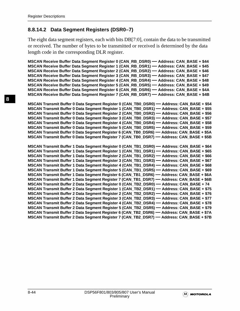
8-44 DSP56F801/803/805/807 User’s Manual�Preliminary
Register Descriptions
8
8.8.14.2 Data Segment Registers (DSR0–7)
The eight data segment registers, each with bits DB[7:0], contain the data to be transmitted or received. The number of bytes to be transmitted or received is determined by the data length code in the corresponding DLR register.
MSCAN Receive Buffer Data Segment Register 0 (CAN_RB_DSR0) — Address: CAN_BASE + $44MSCAN Receive Buffer Data Segment Register 1 (CAN_RB_DSR1) — Address: CAN_BASE + $45MSCAN Receive Buffer Data Segment Register 2 (CAN_RB_DSR2) — Address: CAN_BASE + $46MSCAN Receive Buffer Data Segment Register 3 (CAN_RB_DSR3) — Address: CAN_BASE + $47MSCAN Receive Buffer Data Segment Register 4 (CAN_RB_DSR4) — Address: CAN_BASE + $48MSCAN Receive Buffer Data Segment Register 5 (CAN_RB_DSR5) — Address: CAN_BASE + $49MSCAN Receive Buffer Data Segment Register 6 (CAN_RB_DSR6) — Address: CAN_BASE + $4AMSCAN Receive Buffer Data Segment Register 7 (CAN_RB_DSR7) — Address: CAN_BASE + $4B
MSCAN Transmit Buffer 0 Data Segment Register 0 (CAN_TB0_DSR0) — Address: CAN_BASE + $54MSCAN Transmit Buffer 0 Data Segment Register 1 (CAN_TB0_DSR1) — Address: CAN_BASE + $55MSCAN Transmit Buffer 0 Data Segment Register 2 (CAN_TB0_DSR2) — Address: CAN_BASE + $56MSCAN Transmit Buffer 0 Data Segment Register 3 (CAN_TB0_DSR3) — Address: CAN_BASE + $57MSCAN Transmit Buffer 0 Data Segment Register 4 (CAN_TB0_DSR4) — Address: CAN_BASE + $58MSCAN Transmit Buffer 0 Data Segment Register 5 (CAN_TB0_DSR5) — Address: CAN_BASE + $59MSCAN Transmit Buffer 0 Data Segment Register 6 (CAN_TB0_DSR6) — Address: CAN_BASE + $5AMSCAN Transmit Buffer 0 Data Segment Register 7 (CAN_TB0_DSR7) — Address: CAN_BASE + $5B
MSCAN Transmit Buffer 1 Data Segment Register 0 (CAN_TB1_DSR0) — Address: CAN_BASE + $64MSCAN Transmit Buffer 1 Data Segment Register 1 (CAN_TB1_DSR1) — Address: CAN_BASE + $65MSCAN Transmit Buffer 1 Data Segment Register 2 (CAN_TB1_DSR2) — Address: CAN_BASE + $66MSCAN Transmit Buffer 1 Data Segment Register 3 (CAN_TB1_DSR3) — Address: CAN_BASE + $67MSCAN Transmit Buffer 1 Data Segment Register 4 (CAN_TB1_DSR4) — Address: CAN_BASE + $68MSCAN Transmit Buffer 1 Data Segment Register 5 (CAN_TB1_DSR5) — Address: CAN_BASE + $69MSCAN Transmit Buffer 1 Data Segment Register 6 (CAN_TB1_DSR6) — Address: CAN_BASE + $6AMSCAN Transmit Buffer 1 Data Segment Register 7 (CAN_TB1_DSR7) — Address: CAN_BASE + $6BMSCAN Transmit Buffer 2 Data Segment Register 0 (CAN_TB2_DSR0) — Address: CAN_BASE + 74 MSCAN Transmit Buffer 2 Data Segment Register 1 (CAN_TB2_DSR1) — Address: CAN_BASE + $75MSCAN Transmit Buffer 2 Data Segment Register 2 (CAN_TB2_DSR2) — Address: CAN_BASE + $76MSCAN Transmit Buffer 2 Data Segment Register 3 (CAN_TB2_DSR3) — Address: CAN_BASE + $77MSCAN Transmit Buffer 2 Data Segment Register 4 (CAN_TB2_DSR4) — Address: CAN_BASE + $78MSCAN Transmit Buffer 2 Data Segment Register 5 (CAN_TB2_DSR5) — Address: CAN_BASE + $79MSCAN Transmit Buffer 2 Data Segment Register 6 (CAN_TB2_DSR6) — Address: CAN_BASE + $7AMSCAN Transmit Buffer 2 Data Segment Register 7 (CAN_TB2_DSR7) — Address: CAN_BASE + $7B
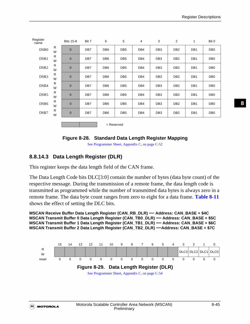
Register Descriptions
�Motorola Scalable Controller Area Network (MSCAN) 8-45
Preliminary
8
Figure 8-28. Standard Data Length Register MappingSee Programmer Sheet, Appendix C, on page C-52
8.8.14.3 Data Length Register (DLR)
This register keeps the data length field of the CAN frame.
The Data Length Code bits DLC[3:0] contain the number of bytes (data byte count) of the respective message. During the transmission of a remote frame, the data length code is transmitted as programmed while the number of transmitted data bytes is always zero in a remote frame. The data byte count ranges from zero to eight for a data frame. Table 8-11 shows the effect of setting the DLC bits.
MSCAN Receive Buffer Data Length Register (CAN_RB_DLR) — Address: CAN_BASE + $4CMSCAN Transmit Buffer 0 Data Length Register (CAN_TB0_DLR) — Address: CAN_BASE + $5CMSCAN Transmit Buffer 1 Data Length Register (CAN_TB1_DLR) — Address: CAN_BASE + $6CMSCAN Transmit Buffer 2 Data Length Register (CAN_TB2_DLR) —Address: CAN_BASE + $7C
Figure 8-29. Data Length Register (DLR)See Programmer Sheet, Appendix C, on page C-54
Register name Bits 15-8 Bit 7 6 5 4 3 2 1 Bit 0
DSR0R
0 DB7 DB6 DB5 DB4 DB3 DB2 DB1 DB0W
DSR1R
0 DB7 DB6 DB5 DB4 DB3 DB2 DB1 DB0W
DSR2R
0 DB7 DB6 DB5 DB4 DB3 DB2 DB1 DB0W
DSR3R
0 DB7 DB6 DB5 DB4 DB3 DB2 DB1 DB0W
DSR4R
0 DB7 DB6 DB5 DB4 DB3 DB2 DB1 DB0W
DSR5R
0 DB7 DB6 DB5 DB4 DB3 DB2 DB1 DB0W
DSR6R
0 DB7 DB6 DB5 DB4 DB3 DB2 DB1 DB0W
DSR7R
0 DB7 DB6 DB5 DB4 DB3 DB2 DB1 DB0W
= Reserved
15 14 13 12 11 10 9 8 7 6 5 4 3 2 1 0
RDLC3 DLC2 DLC1 DLC0
W
reset 0 0 0 0 0 0 0 0 0 0 0 0 0 0 0 0
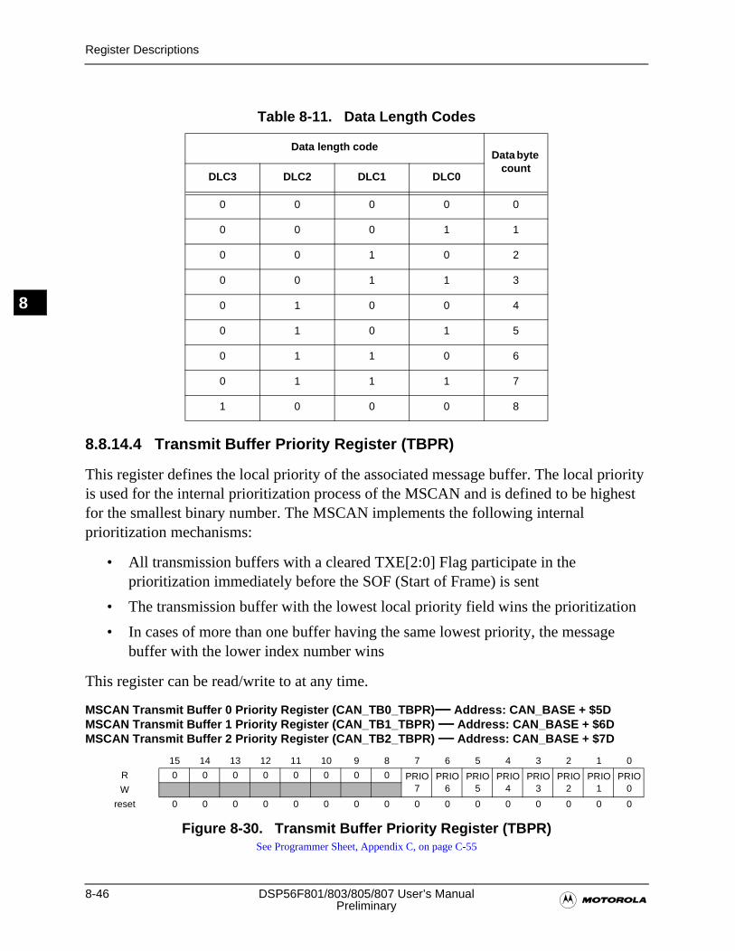
8-46 DSP56F801/803/805/807 User’s Manual�Preliminary
Register Descriptions
8
8.8.14.4 Transmit Buffer Priority Register (TBPR)
This register defines the local priority of the associated message buffer. The local priority is used for the internal prioritization process of the MSCAN and is defined to be highest for the smallest binary number. The MSCAN implements the following internal prioritization mechanisms:
• All transmission buffers with a cleared TXE[2:0] Flag participate in the prioritization immediately before the SOF (Start of Frame) is sent
• The transmission buffer with the lowest local priority field wins the prioritization
• In cases of more than one buffer having the same lowest priority, the message buffer with the lower index number wins
This register can be read/write to at any time.
MSCAN Transmit Buffer 0 Priority Register (CAN_TB0_TBPR)— Address: CAN_BASE + $5DMSCAN Transmit Buffer 1 Priority Register (CAN_TB1_TBPR) — Address: CAN_BASE + $6DMSCAN Transmit Buffer 2 Priority Register (CAN_TB2_TBPR) — Address: CAN_BASE + $7D
Table 8-11. Data Length Codes
Data length codeData byte
countDLC3 DLC2 DLC1 DLC0
0 0 0 0 0
0 0 0 1 1
0 0 1 0 2
0 0 1 1 3
0 1 0 0 4
0 1 0 1 5
0 1 1 0 6
0 1 1 1 7
1 0 0 0 8
15 14 13 12 11 10 9 8 7 6 5 4 3 2 1 0
R 0 0 0 0 0 0 0 0 PRIO7
PRIO6
PRIO5
PRIO4
PRIO3
PRIO2
PRIO1
PRIO0W
reset 0 0 0 0 0 0 0 0 0 0 0 0 0 0 0 0
Figure 8-30. Transmit Buffer Priority Register (TBPR)See Programmer Sheet, Appendix C, on page C-55
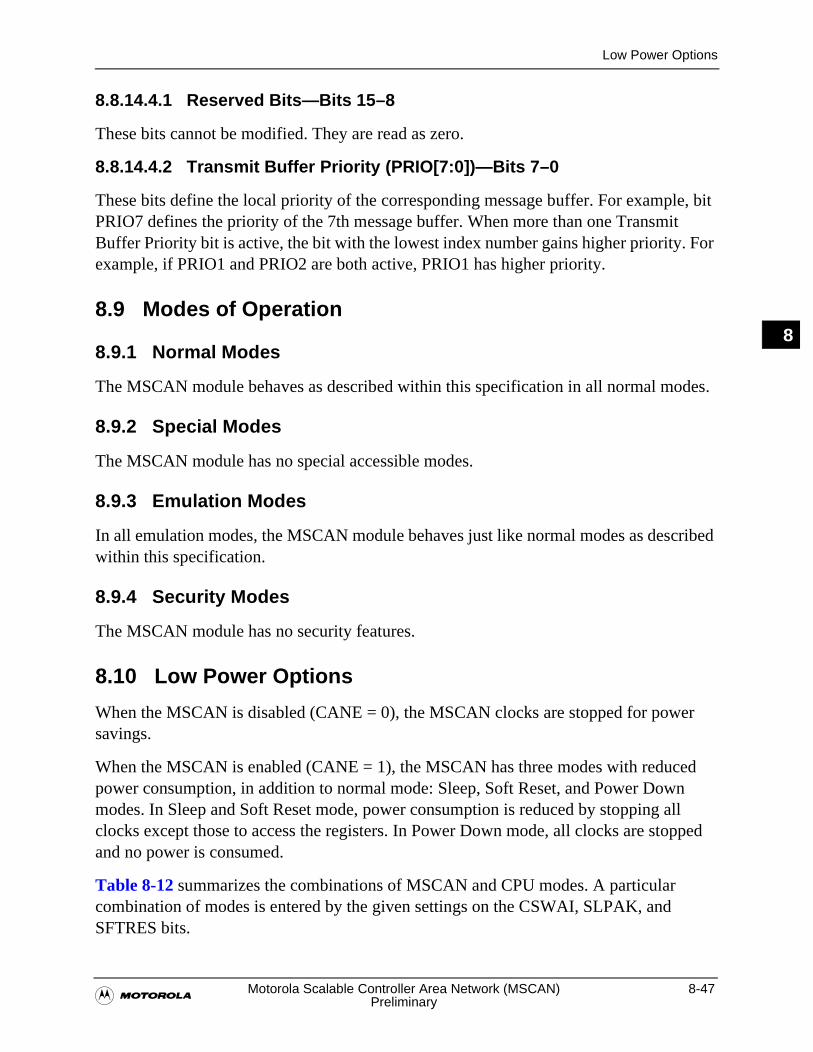
Low Power Options
�Motorola Scalable Controller Area Network (MSCAN) 8-47
Preliminary
8
8.8.14.4.1 Reserved Bits—Bits 15–8
These bits cannot be modified. They are read as zero.
8.8.14.4.2 Transmit Buffer Priority (PRIO[7:0])—Bits 7–0
These bits define the local priority of the corresponding message buffer. For example, bit PRIO7 defines the priority of the 7th message buffer. When more than one Transmit Buffer Priority bit is active, the bit with the lowest index number gains higher priority. For example, if PRIO1 and PRIO2 are both active, PRIO1 has higher priority.
8.9 Modes of Operation
8.9.1 Normal Modes
The MSCAN module behaves as described within this specification in all normal modes.
8.9.2 Special Modes
The MSCAN module has no special accessible modes.
8.9.3 Emulation Modes
In all emulation modes, the MSCAN module behaves just like normal modes as described within this specification.
8.9.4 Security Modes
The MSCAN module has no security features.
8.10 Low Power Options
When the MSCAN is disabled (CANE = 0), the MSCAN clocks are stopped for power savings.
When the MSCAN is enabled (CANE = 1), the MSCAN has three modes with reduced power consumption, in addition to normal mode: Sleep, Soft Reset, and Power Down modes. In Sleep and Soft Reset mode, power consumption is reduced by stopping all clocks except those to access the registers. In Power Down mode, all clocks are stopped and no power is consumed.
Table 8-12 summarizes the combinations of MSCAN and CPU modes. A particular combination of modes is entered by the given settings on the CSWAI, SLPAK, and SFTRES bits.
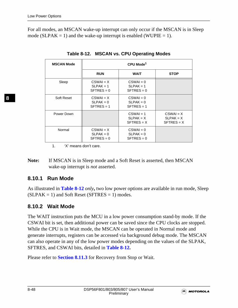
8-48 DSP56F801/803/805/807 User’s Manual�Preliminary
Low Power Options
8
For all modes, an MSCAN wake-up interrupt can only occur if the MSCAN is in Sleep mode (SLPAK = 1) and the wake-up interrupt is enabled (WUPIE = 1).
Note: If MSCAN is in Sleep mode and a Soft Reset is asserted, then MSCAN wake-up interrupt is not asserted.
8.10.1 Run Mode
As illustrated in Table 8-12 only, two low power options are available in run mode, Sleep (SLPAK = 1) and Soft Reset (SFTRES = 1) modes.
8.10.2 Wait Mode
The WAIT instruction puts the MCU in a low power consumption stand-by mode. If the CSWAI bit is set, then additional power can be saved since the CPU clocks are stopped. While the CPU is in Wait mode, the MSCAN can be operated in Normal mode and generate interrupts, registers can be accessed via background debug mode. The MSCAN can also operate in any of the low power modes depending on the values of the SLPAK, SFTRES, and CSWAI bits, detailed in Table 8-12.
Please refer to Section 8.11.3 for Recovery from Stop or Wait.
Table 8-12. MSCAN vs. CPU Operating Modes
MSCAN Mode CPU Mode1
1. ‘X’ means don’t care.
RUN WAIT STOP
Sleep CSWAI = XSLPAK = 1
SFTRES = 0
CSWAI = 0SLPAK = 1
SFTRES = 0
Soft Reset CSWAI = XSLPAK = 0
SFTRES = 1
CSWAI = 0SLPAK = 0
SFTRES = 1
Power Down CSWAI = 1SLPAK = X
SFTRES = X
CSWAI = XSLPAK = X
SFTRES = X
Normal CSWAI = XSLPAK = 0
SFTRES = 0
CSWAI = 0SLPAK = 0
SFTRES = 0
Low Power Options
�Motorola Scalable Controller Area Network (MSCAN) 8-49
Preliminary
8
Note: Important: It is possible for MSCAN to wake-up the CPU from Wait mode if the following sequence is followed by the system designer.
1. MSCAN is put into Sleep mode and discussed in Section 8.10.4
2. CSWAI control bit is set in CANCTL0 Register. To Set CAN Stops in Wait mode
3. MSCAN is put into Wait mode
In this case, MSCAN would generate a wake-up interrupt signal to the CPU on sensing any bus event of CAN Bus. Glitches of less than 5 µs are filtered out. This wake-up design uses the Crystal Oscillator Clock directly and also the whole path for assertion of wake-up interrupt is asynchronous with respect to the System operation.
8.10.3 Stop Mode
The STOP instruction puts the MCU in a low power consumption stand-by mode. In Stop mode, the MSCAN operates in Power Down mode regardless of the value of the SLPAK, SFTRES, and CSWAI bits. See Table 8-12.
Please refer to Section 8.11.3 for Recovery from Stop mode.
Note: Important: It is possible for MSCAN to wake-up the CPU from Stop mode, if and only if the following sequence is followed by the system designer.
1. MSCAN is put into Sleep mode, discussed in Section 8.10.4 below
2. MSCAN is put into Stop mode
In this case, MSCAN would generate a wake-up interrupt signal to the CPU on sensing any bus event of CAN Bus. Glitches of less than five µs are filtered out. Our wake-up design uses the Crystal Oscillator Clock directly and also the whole path for assertion of wake-up interrupt is asynchronous with respect to the System operation.
8.10.4 Sleep Mode
The CPU can request the MSCAN to enter this low power mode by asserting the SLPRQ bit in the CANCTL0 register. See Figure 8-31. The time when the MSCAN enters Sleep mode depends on its activity:
• If it is transmitting, it continues to transmit until the entire message is transmitted and then goes into Sleep mode
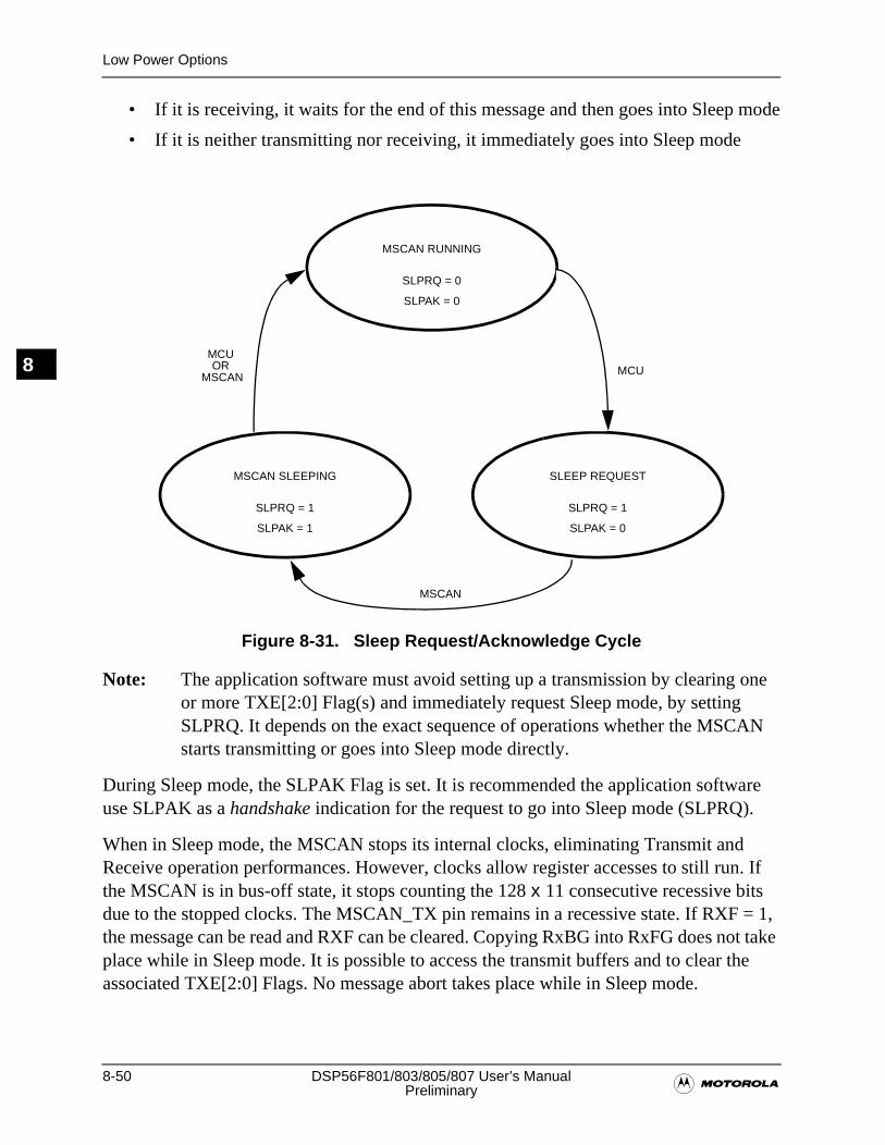
8-50 DSP56F801/803/805/807 User’s Manual�Preliminary
Low Power Options
8
• If it is receiving, it waits for the end of this message and then goes into Sleep mode
• If it is neither transmitting nor receiving, it immediately goes into Sleep mode
Figure 8-31. Sleep Request/Acknowledge Cycle
Note: The application software must avoid setting up a transmission by clearing one or more TXE[2:0] Flag(s) and immediately request Sleep mode, by setting SLPRQ. It depends on the exact sequence of operations whether the MSCAN starts transmitting or goes into Sleep mode directly.
During Sleep mode, the SLPAK Flag is set. It is recommended the application software use SLPAK as a handshake indication for the request to go into Sleep mode (SLPRQ).
When in Sleep mode, the MSCAN stops its internal clocks, eliminating Transmit and Receive operation performances. However, clocks allow register accesses to still run. If the MSCAN is in bus-off state, it stops counting the 128 x 11 consecutive recessive bits due to the stopped clocks. The MSCAN_TX pin remains in a recessive state. If RXF = 1, the message can be read and RXF can be cleared. Copying RxBG into RxFG does not take place while in Sleep mode. It is possible to access the transmit buffers and to clear the associated TXE[2:0] Flags. No message abort takes place while in Sleep mode.
MSCAN RUNNING
SLPRQ = 0
SLPAK = 0
SLEEP REQUEST
SLPRQ = 1
SLPAK = 0
MSCAN SLEEPING
SLPRQ = 1
SLPAK = 1
MCU
MSCAN
MCU OR
MSCAN
Low Power Options
�Motorola Scalable Controller Area Network (MSCAN) 8-51
Preliminary
8
The MSCAN leaves Sleep mode, wake-up, when
• bus activity occurs, or
• the MCU clears the SLPRQ bit, or
• the MCU sets the SFTRES bit
Note: The MCU cannot clear the SLPRQ bit before the MSCAN has entered Sleep mode (SLPAK = 1).
Note: Important: It is possible for MSCAN to wake-up the CPU from Wait mode, if the following sequence is followed by the system designer.
1. MSCAN is put into Sleep mode and discussed in Section 8.10.4.
2. CSWAI control bit is set in CANCTL0 Register. To Set CAN Stops in Wait mode.
3. MSCAN is put into Wait mode.
In this case, MSCAN would generate a wake-up interrupt signal to the CPU on sensing any bus event of CAN Bus. Glitches of less than five µ are filtered out. This wake-up design uses the Crystal Oscillator Clock directly and also the whole path for assertion of wake-up interrupt is asynchronous.
After wake-up, the MSCAN waits for 11 consecutive recessive bits to synchronize to the bus. As a consequence, if the MSCAN is awakened by a CAN frame, this frame is not received. The receive message buffers (RxFG and RxBG) contain messages if they were received before Sleep mode was entered. All pending actions will be executed upon wake-up; copying of RxBG into RxFG, message aborts and message transmissions. If the MSCAN is still in bus-off state after Sleep mode was left, it continues counting the 128 x 11 consecutive recessive bits.
Note: It is to be noted MSCAN wakes up from Sleep mode, when SOFTRES bit in CANCTL0 register is asserted. However, this mechanism is not a recommended approach for wake-up, because after assertion of SOFTRES bit in CANCTL0 register, all registers come to a known default reset state. Also in this approach, pending actions before entering into sleep mode, for example, copying of RxBG into RxFG will not be executed, as MSCAN would already be in SOFTRES state.
8-52 DSP56F801/803/805/807 User’s Manual�Preliminary
Low Power Options
8
8.10.5 Soft Reset Mode
In Soft Reset mode, any ongoing transmission or reception is aborted and synchronization to the bus is lost potentially causing CAN protocol violations. The MSCAN drives the MSCAN_TX pin to a recessive state to protect the CAN bus.
Note: The user must ensure the MSCAN is not active when Soft Reset mode is entered. The recommended procedure is to bring the MSCAN into Sleep mode before setting the SFTRES bit in the CANCTL0 register.
In Soft Reset mode, the MSCAN is stopped. However, registers can still be accessed. This mode is used to initialize the module configuration, bit timing, and the CAN message filter. See Section 8.8.1 for a description of the Soft Reset mode.
8.10.6 Power Down Mode
The MSCAN is in Power Down mode when:
• The CPU is in Stop mode or
• The CPU is in Wait mode and the CSWAI bit is set
When entering the Power Down mode, the MSCAN immediately stops all ongoing transmissions and receptions, potentially causing CAN protocol violations. Please refer to Table 8-12.
Note: The user must ensure the MSCAN is not active when Power Down mode is entered. The recommended procedure is to bring the MSCAN into Sleep mode before the STOP or WAIT instruction, if CSWAI is set, is executed.
To protect the CAN bus system from fatal consequences of violations to the above rule, the MSCAN drives the MSCAN_TX pin into a recessive state.
In Power Down mode, all clocks are stopped and no registers can be accessed.
8.10.7 Programmable Wake-Up Function
The MSCAN can be programmed to apply a low-pass filter function to the MSCAN_RX input line while in Sleep mode. See control bit WUPM in Section 8.8.2. This feature can be used to protect the MSCAN from wake-up due to short glitches on the CAN bus lines. Such glitches can result from electromagnetic interference within noisy environments. The wake-up filter function, filtering the glitches on CAN Bus of duration less than five µs, is programmable through the bit wake-up mode in CANCTL1 Register.
Interrupt Operation
�Motorola Scalable Controller Area Network (MSCAN) 8-53
Preliminary
8
8.11 Interrupt Operation
The MSCAN supports four interrupt vectors mapped onto eleven different interrupt sources, any of which can be individually masked. For details, see Section 8.8.5 to Section 8.8.8.
• Transmit Interrupt—At least one of the three transmit buffers, TB0, TB1, TB2, is empty, that is, not scheduled. It can be loaded to schedule a message for transmission. The TXE[2:0] Flag of the empty message buffer is set. See Table 8-10
• Receive Interrupt—A message is successfully received and loaded into the foreground receive buffer. This interrupt is generated immediately after recognizing the EOF symbol. The RXF Flag is set
• Wake-up Interrupt—Activity on the CAN bus occurred during MSCAN internal Sleep mode
• Error Interrupt—An overrun, error, or warning condition occurred. The MSCAN Receiver Flag Register (CANRFLG) indicates one of the following conditions:
— Overrun—An overrun condition has occurred, and described in Section 8.7.1.3
— Receiver Warning—The Receive Error Counter has reached the CPU Warning limit of 96
— Transmitter Warning ---The Transmit Error Counter has reached the CPU Warning limit of 96
— Receiver Error Passive—The Receive Error Counter has exceeded the Error Passive limit of 127 and MSCAN has gone to Error Passive state
— Transmitter Error Passive—The Transmit Error Counter has exceeded the Error Passive limit of 127 and MSCAN has gone to Error Passive state
— Bus Off—The Transmit Error Counter has exceeded 255 and MSCAN has gone to Bus-Off state
Note: Error Interrupt signal to CPU is asserted when exceeding the threshold condition for interrupt and when dropping below the threshold condition for each cause of the Error Interrupt generation. This ensures CPU comes to know the updated status of the cause of the Error Interrupt generation and hence CPU need not waste cycles in just polling for the event.
For Instance, Error Interrupt is asserted when Transmitter Error Count crosses the threshold of 96, TX Warning Error, from <96 to >96, and also from >96 to <96. Similarly, for Receiver Warning case, when the Rx error count is crossing
8-54 DSP56F801/803/805/807 User’s Manual�Preliminary
Interrupt Operation
8
from <128 to >128 as well as from >128 to <128, Error Interrupt is asserted. Similar rules apply to other Error Flags.
When CPU writes one into any of the Error Interrupt Causing Flags, the Error Interrupt signal gets denied, if the interrupt is already asserted, even though the condition to set the flag continues to remain active. That means, a write of one by CPU will shield only the interrupt signal to CPU and does not update the status of the flag.
8.11.1 Interrupt Acknowledge
Interrupts are directly associated with one or more status flags in either the MSCAN Receiver Flag Register (CANRFLG) or the MSCAN Transmitter Flag Register (CANTFLG). Interrupts are pending as long as one of the corresponding flags is set. Interrupt flags must be reset within the Interrupt Handler to re-enable the interrupt. The flags are reset by writing a one to the corresponding bit in the flag register. A flag cannot be cleared if the respective condition still prevails, except in the case of an Error Interrupt.
If an Error Interrupt is the cause of the interrupt, the CPU has to write one in the corresponding flags in the above registers to clear the Interrupt Signal to the CPU. In this case, even though Error Interrupt Flags status is set, that is, the Error Counter Value is still above the defined threshold value, interrupt still gets denied when the CPU writes one into the corresponding bit positions causing Error Interrupt.
Note: There is a one cycle delay in the clearing of the interrupt request once the interrupt flag has been cleared. It is recommended to clear the interrupt flag early in the interrupt handler routine.
Note: Bit manipulation instructions (BSET) must not be used to clear interrupt flags.
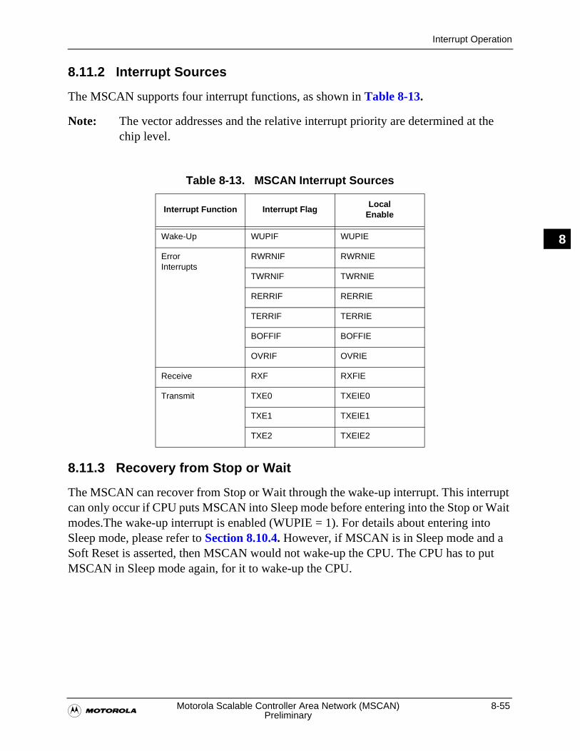
Interrupt Operation
�Motorola Scalable Controller Area Network (MSCAN) 8-55
Preliminary
8
8.11.2 Interrupt Sources
The MSCAN supports four interrupt functions, as shown in Table 8-13.
Note: The vector addresses and the relative interrupt priority are determined at the chip level.
8.11.3 Recovery from Stop or Wait
The MSCAN can recover from Stop or Wait through the wake-up interrupt. This interrupt can only occur if CPU puts MSCAN into Sleep mode before entering into the Stop or Wait modes.The wake-up interrupt is enabled (WUPIE = 1). For details about entering into Sleep mode, please refer to Section 8.10.4. However, if MSCAN is in Sleep mode and a Soft Reset is asserted, then MSCAN would not wake-up the CPU. The CPU has to put MSCAN in Sleep mode again, for it to wake-up the CPU.
Table 8-13. MSCAN Interrupt Sources
Interrupt Function Interrupt FlagLocal
Enable
Wake-Up WUPIF WUPIE
ErrorInterrupts
RWRNIF RWRNIE
TWRNIF TWRNIE
RERRIF RERRIE
TERRIF TERRIE
BOFFIF BOFFIE
OVRIF OVRIE
Receive RXF RXFIE
Transmit TXE0 TXEIE0
TXE1 TXEIE1
TXE2 TXEIE2

8-56 DSP56F801/803/805/807 User’s Manual�Preliminary
Interrupt Operation
8
�Analog-to-Digital Converter (ADC) 9-1
Preliminary
9
Chapter 9Analog-to-Digital Converter (ADC)

9-2 DSP56F801/803/805/807 User’s Manual�Preliminary
9
Features
�Analog-to-Digital Converter (ADC) 9-3
Preliminary
9
9.1 Introduction
The DSP56F801, DSP56F803, and DSP56F805 each have a dual, 4-input, Analog-to-Digital Converter (ADC) named ADCA totaling eight analog inputs. The DSP56F807 has two dual, 4-input, 12-bit ACDs named ADCA and ADCB, totaling 16 analog inputs.
9.2 Features
Each Analog-to-Digital Converter (ADC) consists of a digital control module and two analog Sample and Hold (S/H) circuits. The ADC features the following:
• 12-bit resolution
• Sampling rate up to 1.66 million samples per second1
• Maximum ADC Clock frequency is 5MHz with 200 ns period
• Single conversion time of 8.5 ADC Clock cycles (8.5 x 200 ns = 1.7 µs)
• Additional conversion time of 6 ADC clock cycles (6 x 200 ns = 1.2 µs)
• Eight conversions in 26.5 ADC Clock cycles (26.5 x 200 ns = 5.3 µs) using Simultaneous mode
• ADC can be synchronized to the PWM via the SYNC signal
• Simultaneous or sequential sampling
• Internal multiplexer to select two of eight inputs
• Ability to sequentially scan and store up to eight measurements
• Ability to simultaneously sample and hold two inputs
• Optional interrupts at end of scan, if an out-of-range limit is exceeded or at zero crossing
• Optional sample correction by subtracting a pre-programmed offset value
• Signed or unsigned result
• Single ended or differential inputs
1. Once in Loop mode, the time between each conversion is 6 ADC Clock cycles (1.2 µs). UsingSimultaneous conversion, two samples can be obtained in 1.2 µs. Samples per second is calculated accordingto 1.2 µs per two samples or 1666666 samples per second.
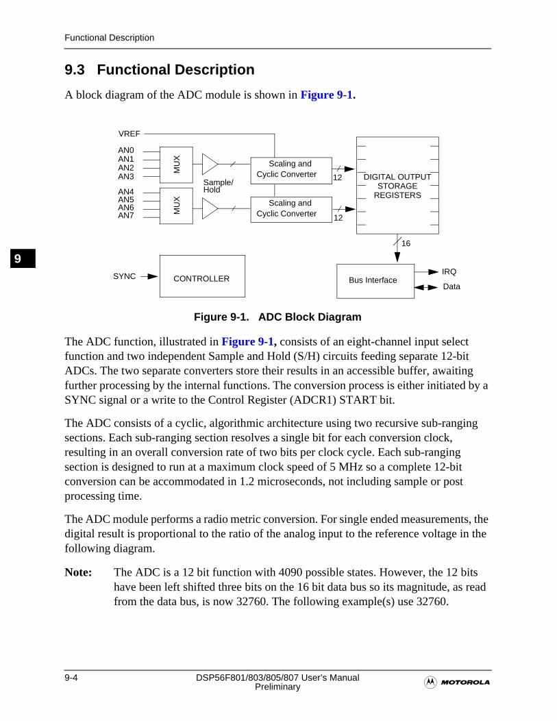
9-4 DSP56F801/803/805/807 User’s Manual�Preliminary
Functional Description
9
9.3 Functional Description
A block diagram of the ADC module is shown in Figure 9-1.
Figure 9-1. ADC Block Diagram
The ADC function, illustrated in Figure 9-1, consists of an eight-channel input select function and two independent Sample and Hold (S/H) circuits feeding separate 12-bit ADCs. The two separate converters store their results in an accessible buffer, awaiting further processing by the internal functions. The conversion process is either initiated by a SYNC signal or a write to the Control Register (ADCR1) START bit.
The ADC consists of a cyclic, algorithmic architecture using two recursive sub-ranging sections. Each sub-ranging section resolves a single bit for each conversion clock, resulting in an overall conversion rate of two bits per clock cycle. Each sub-ranging section is designed to run at a maximum clock speed of 5 MHz so a complete 12-bit conversion can be accommodated in 1.2 microseconds, not including sample or post processing time.
The ADC module performs a radio metric conversion. For single ended measurements, the digital result is proportional to the ratio of the analog input to the reference voltage in the following diagram.
Note: The ADC is a 12 bit function with 4090 possible states. However, the 12 bits have been left shifted three bits on the 16 bit data bus so its magnitude, as read from the data bus, is now 32760. The following example(s) use 32760.
MU
XDIGITAL OUTPUT
STORAGEREGISTERS
CONTROLLER
VREF
SYNC IRQ
16
Sample/M
UX
Scaling andCyclic Converter
Scaling andCyclic Converter
DataBus Interface
12
12
AN0AN1AN2AN3
AN4AN5AN6AN7
Hold
Functional Description
�Analog-to-Digital Converter (ADC) 9-5
Preliminary
9
:
Note: The result is rounded to the nearest LSB.
Vin = Applied voltage
Vref = External pin on the device
Starting a single conversion actually begins a sequence of conversions, or a scan. A conversion, or scan, can sample and convert up to eight unique single-ended channels, up to four differential channel pairs, or any combination of these.
The ADC can be configured to perform a single scan and halt, perform a scan whenever triggered, or perform the programmed scan sequence repeatedly until manually stopped.
The dual ADC can be configured for either sequential or simultaneous conversion. When configured for sequential configuration, up to eight channels, single-ended connection, can be sampled and stored in any order specified by the Channel List Register. During a simultaneous conversion, both S/H circuits are used to capture two different channels at the same time. This configuration places the restriction a single channel may not be sampled by both S/H circuits simultaneously.
The Channel List Register is programmed with the scan order of the desired channels.
Optional interrupts can be generated at the end of the scan sequence. The optional interrupt is used if a channel is out of range. Range is determined by the High and Low Limit registers, or at several different zero crossing conditions.
The method for initiating a conversion, or a scan consisting of multiple conversions, is programmable. It can be set to be either the SYNC signal or a write to the ADCR1 Control Register START bit. If a scan is initiated while another scan is in process, the start signal is ignored until the conversion is complete, or when CIP breaks to 0.
9.3.1 Differential Inputs
The number of conversions in a scan is programmable from one to eight separate channels when all inputs are configured as single-ended, or programmable from one to four, if all inputs are configured as differential.
Note: The ADC is a 12 bit function with 4090 possible states. However, the 12 bits have been left shifted three bits on the 16 bit data bus so its magnitude, as read from the data bus, is now 32760. The following example(s) use 32760.
ValueRead32760
----------------------------- VREF× SingleEndedVoltage=
9-6 DSP56F801/803/805/807 User’s Manual�Preliminary
Functional Description
9
When converting differential measurements, the following formula is useful:
Here are some examples:
Typical Reading:
Most Negative Reading Possible:
Most Positive Reading Possible:
A Zero reading (hex values shown):
To get dependable data from differential measurements, the voltage applied to the +/- inputs must be symmetric about VDDA/2. Also the VREF input must be tired to the same potential as VDDA.
6.6VValueRead( )
32760----------------------------------× 3.3V– DifferentialVoltage=
6.6V2211232760---------------×
3.3V– 1.15V=
6.6V0
32760---------------×
3.3V– 3.3V–=
6.6V3276032760---------------×
3.3V– 3.3V=
6.6V3FFC7FF8---------------×
3.3V– 0V=
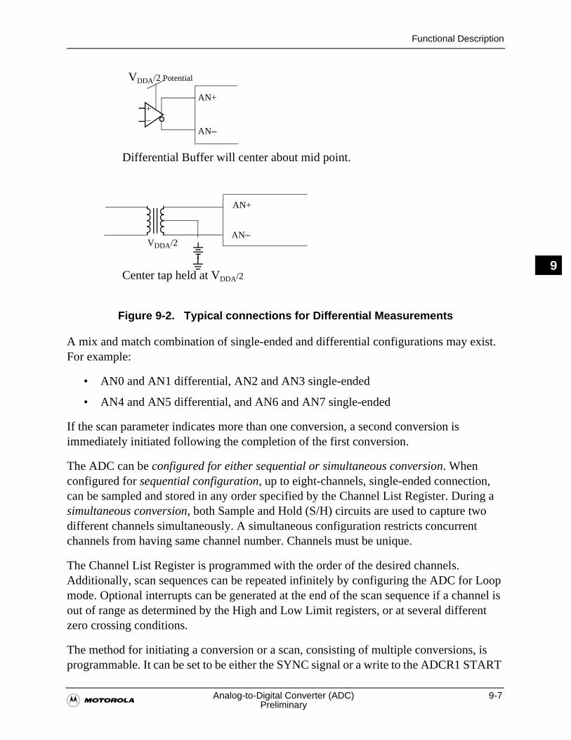
Functional Description
�Analog-to-Digital Converter (ADC) 9-7
Preliminary
9
Figure 9-2. Typical connections for Differential Measurements
A mix and match combination of single-ended and differential configurations may exist. For example:
• AN0 and AN1 differential, AN2 and AN3 single-ended
• AN4 and AN5 differential, and AN6 and AN7 single-ended
If the scan parameter indicates more than one conversion, a second conversion is immediately initiated following the completion of the first conversion.
The ADC can be configured for either sequential or simultaneous conversion. When configured for sequential configuration, up to eight-channels, single-ended connection, can be sampled and stored in any order specified by the Channel List Register. During a simultaneous conversion, both Sample and Hold (S/H) circuits are used to capture two different channels simultaneously. A simultaneous configuration restricts concurrent channels from having same channel number. Channels must be unique.
The Channel List Register is programmed with the order of the desired channels. Additionally, scan sequences can be repeated infinitely by configuring the ADC for Loop mode. Optional interrupts can be generated at the end of the scan sequence if a channel is out of range as determined by the High and Low Limit registers, or at several different zero crossing conditions.
The method for initiating a conversion or a scan, consisting of multiple conversions, is programmable. It can be set to be either the SYNC signal or a write to the ADCR1 START
+–
AN+
AN–
AN+
AN–VDDA/2
Differential Buffer will center about mid point.
Center tap held at VDDA/2
VDDA/2 Potential
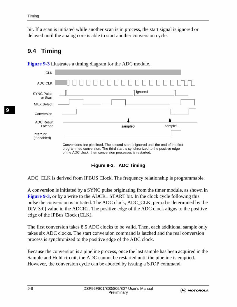
9-8 DSP56F801/803/805/807 User’s Manual�Preliminary
Timing
9
bit. If a scan is initiated while another scan is in process, the start signal is ignored or delayed until the analog core is able to start another conversion cycle.
9.4 Timing
Figure 9-3 illustrates a timing diagram for the ADC module.
Figure 9-3. ADC Timing
ADC_CLK is derived from IPBUS Clock. The frequency relationship is programmable.
A conversion is initiated by a SYNC pulse originating from the timer module, as shown in Figure 9-3, or by a write to the ADCR1 START bit. In the clock cycle following this pulse the conversion is initiated. The ADC clock, ADC_CLK, period is determined by the DIV[3:0] value in the ADCR2. The positive edge of the ADC clock aligns to the positive edge of the IPBus Clock (CLK).
The first conversion takes 8.5 ADC clocks to be valid. Then, each additional sample only takes six ADC clocks. The start conversion command is latched and the real conversion process is synchronized to the positive edge of the ADC clock.
Because the conversion is a pipeline process, once the last sample has been acquired in the Sample and Hold circuit, the ADC cannot be restarted until the pipeline is emptied. However, the conversion cycle can be aborted by issuing a STOP command.
ADC CLK
MUX Select
Conversion
ADC Result
CLK
SYNC Pulse
Latched sample0 sample1
or Start
ignored
Conversions are pipelined. The second start is ignored until the end of the firstprogrammed conversion. The third start is synchronized to the positive edgeof the ADC clock, then conversion processes is restarted.
Interrupt(if enabled)
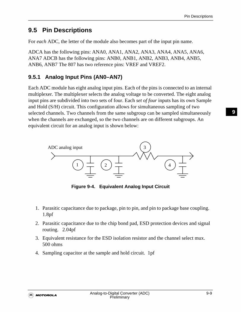
Pin Descriptions
�Analog-to-Digital Converter (ADC) 9-9
Preliminary
9
9.5 Pin Descriptions
For each ADC, the letter of the module also becomes part of the input pin name.
ADCA has the following pins: ANA0, ANA1, ANA2, ANA3, ANA4, ANA5, ANA6, ANA7 ADCB has the following pins: ANB0, ANB1, ANB2, ANB3, ANB4, ANB5, ANB6, ANB7 The 807 has two reference pins: VREF and VREF2.
9.5.1 Analog Input Pins (AN0–AN7)
Each ADC module has eight analog input pins. Each of the pins is connected to an internal multiplexer. The multiplexer selects the analog voltage to be converted. The eight analog input pins are subdivided into two sets of four. Each set of four inputs has its own Sample and Hold (S/H) circuit. This configuration allows for simultaneous sampling of two selected channels. Two channels from the same subgroup can be sampled simultaneously when the channels are exchanged, so the two channels are on different subgroups. An equivalent circuit for an analog input is shown below:
Figure 9-4. Equivalent Analog Input Circuit
1. Parasitic capacitance due to package, pin to pin, and pin to package base coupling. 1.8pf
2. Parasitic capacitance due to the chip bond pad, ESD protection devices and signal routing. 2.04pf
3. Equivalent resistance for the ESD isolation resistor and the channel select mux. 500 ohms
4. Sampling capacitor at the sample and hold circuit. 1pf
1 2
3
4
ADC analog input
9-10 DSP56F801/803/805/807 User’s Manual�Preliminary
Register Summary
9
9.5.2 Voltage Reference Pin (VREF)
The difference between VREF and VSSA, analog ground, provides the reference voltage all analog inputs are measured against. VREF is nominally set to 3.3V. VSSA is nominally set to 0V. The reference voltage ought to be provided from a low noise filtered source. All bypass capacitors must be connected between VREF and VSSA. The reference source should be capable of providing up to 10mA of reference current.
When making absolute measurements, with respect to ground, it is recommended VREF be fixed 100mV below the minimum supply voltage the part is expected to see. Under this condition, the part should be used in the single ended mode only, the differential mode does not correctly function with these conditions.
When tieing VREF to the same potential as VDDA relative measurements are being made with respect to the amplitude of VDDA. It is imperative special precautions be taken assuring the voltage applied to VREF be as noise free as possible. Any noise residing on the VREF voltage is directly transferred to the digital result.
The VREF signal typically takes roughly 10mA and is expected to be as noise free as possible for the ADC to maintain good accuracy. If the analog input signals, being measured by the ADC, exceed either VREF or VSSA, the ADC will produce unpredictable results.
9.5.3 Supply Pins (VDDA, VSSA)
Dedicated power supply pins have been provided for the purposes of reducing noise coupling and to improve accuracy. The power provided to these pins is suggested to come from a low noise filtered source and be capable of providing up to 40mA of current. Uncoupling capacitors ought to be connected between VDDA and VSSA.
9.6 Register Summary
A prefix is added to each register to reflect which ADC module is being accessed: ADCA or ADCB. For example, the ADCR1 for the ADCA module will be called ADCA_ADCR1.
Each DSP56F801/803/805/807 ADC module has the following registers:
• ADC Control Register 1(ADCR1)
• ADC Control Register 2 (ADCR2)
• ADC Zero Crossing Control Register (ADZCC)
• ADC Channel List Register 1(ADLST1)
• ADC Channel List Register 2 (ADLST2)
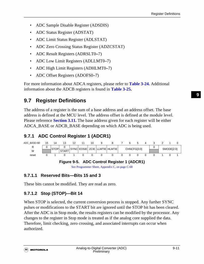
Register Definitions
�Analog-to-Digital Converter (ADC) 9-11
Preliminary
9
• ADC Sample Disable Register (ADSDIS)
• ADC Status Register (ADSTAT)
• ADC Limit Status Register (ADLSTAT)
• ADC Zero Crossing Status Register (ADZCSTAT)
• ADC Result Registers (ADRSLT0–7)
• ADC Low Limit Registers (ADLLMT0–7)
• ADC High Limit Registers (ADHLMT0–7)
• ADC Offset Registers (ADOFS0–7)
For more information about ADCA registers, please refer to Table 3-24. Additional information about the ADCB registers is found in Table 3-25.
9.7 Register Definitions
The address of a register is the sum of a base address and an address offset. The base address is defined at the MCU level. The address offset is defined at the module level. Please reference Section 3.11. The base address given for each register will be either ADCA_BASE or ADCB_BASE depending on which ADC is being used.
9.7.1 ADC Control Register 1 (ADCR1)
9.7.1.1 Reserved Bits—Bits 15 and 3
These bits cannot be modified. They are read as zero.
9.7.1.2 Stop (STOP)—Bit 14
When STOP is selected, the current conversion process is stopped. Any further SYNC pulses or modifications to the START bit are ignored until the STOP bit has been cleared. After the ADC is in Stop mode, the results registers can be modified by the processor. Any changes to the register in Stop mode is treated as if the analog core supplied the data. Therefore, limit checking, zero crossing, and associated interrupts can occur when authorized.
ADC_BASE+$0 15 14 13 12 11 10 9 8 7 6 5 4 3 2 1 0
R 0STOP
0SYNC EOSIE ZCIE LLMTIE HLMTIE CHNCFG[3:0]
0SMODE[2:0]
W START
reset 0 1 0 1 0 0 0 0 0 0 0 0 0 1 0 1
Figure 9-5. ADC Control Register 1 (ADCR1)See Programmer Sheet, Appendix C, on page C-68
9-12 DSP56F801/803/805/807 User’s Manual�Preliminary
Register Definitions
9
• 1 = Stop command issued
• 0 = Normal operation
9.7.1.3 START Conversion (START)—Bit 13
The conversion process is started by a modification to the START bit. This is a write only bit. Once a start command is issued, the conversion process is synchronized and begun on the positive edge of the ADC clock. A START bit re-started while the ADC is in a conversion cycle, is ignored. The ADC must be idle in order for it to recognize a new start-up.
• 1 = Start command is issued
• 0 = No action
9.7.1.4 SYNC Select (SYNC)—Bit 12
A conversion can be began by the SYNC input or by a write to the START bit. A SYNC pulse re-started while the ADC is in a conversion cycle, is ignored. The ADC must be idle in order for it to recognize a new start-up.
• 1 = Use the SYNC input or START bit to initiate a conversion
• 0 = Conversion is initiated by a write to START bit only
9.7.1.5 End Of Scan Interrupt Enable (EOSIE)—Bit 11
This bit begins an interrupt to be generated upon completion of any scan and convert sequence, except for Loop Sequential or Loop Simultaneous modes. This bit is ignored when the ADC is configured for either loop modes.
• 1 = Interrupt enabled
• 0 = Interrupt disabled
9.7.1.6 Zero Crossing Interrupt Enable (ZCIE)—Bit 10
This bit starts the optional interrupt if the current result value has a sign change from the previous result as configured by the ADZCC Register.
• 1 = Interrupt enabled
• 0 = Interrupt disabled
Register Definitions
�Analog-to-Digital Converter (ADC) 9-13
Preliminary
9
9.7.1.7 Low Limit Interrupt Enable (LLMTIE)—Bit 9
This bit enables the optional interrupt when the current result value is less than the Low Limit register value. The raw result value is compared to ADLLMT, the Low Limit Register, bits LLMT[11:0], before the offset register value is subtracted.
• 1 = Interrupt enabled
• 0 = Interrupt disabled
9.7.1.8 High Limit Interrupt Enable (HLMTIE)—Bit 8
This bit confirms the optional interrupt if the current result value is greater than the High Limit register value. The raw result value is compared to ADHLMT, the High Limit Register, bits HLMT[11:0], before the offset register value is subtracted.
• 1 = Interrupt enabled
• 0 = Interrupt disabled
9.7.1.9 Channel Configure (CHNCFG[3:0])—Bits 7–4
The inputs can be configured for either Single Ended or Differential.
• xxx1 = AN0–AN1 configured as differential input. (AN0 is + and AN1 is –)
• xxx0 = AN0–AN1 configured as single ended inputs.
• xx1x = AN2–AN3 configured as differential input. (AN2 is + and AN3 is –)
• xx0x = AN2–AN3 configured as single input.
• x1xx = AN4–AN5 configured as differential inputs. (AN4 is + and AN5 is –)
• x0xx = AN4–AN5 configured as single ended inputs.
• 1xxx = AN6–AN7 configured as differential inputs. (AN6 is + and AN7 is –)
• 0xxx = AN6–AN7 configured as single ended inputs.
9.7.1.10 Scan Mode (SMODE[2:0])—Bits 2–0
A conversion sequence can be begun by asserting the ADCR1 START bit, or by a SYNC pulse. A conversion sequence can take up to eight unique samples. These eight sample slots are supported by the ADSDIS register. A sample sequence is terminated when the first disabled sample is encountered. Analog input channels are assigned to each of the eight sample slots by the ADLST1 and ADLST2 registers. A conversion sequence can be run through just once, every time a trigger occurs or loop continuously. Samples may be taken one at a time, sequentially, or two at a time, simultaneously.
9-14 DSP56F801/803/805/807 User’s Manual�Preliminary
Register Definitions
9
• 000 = Once SequentialUpon START or a first SYNC signal, samples are taken one at a time starting with SAMPLE0, until a first disabled sample is encountered. If no disabled sample is encountered, conversion concludes after the SAMPLE7
• 001 = Once SimultaneousUpon START or a first SYNC signal, samples are taken two at a time, in the order: SAMPLE0/4, SAMPLE1/5, SAMPLE2/6, and SAMPLE3/7. The sample sequence will stop at SAMPLE3/7, or as soon as any disabled sample slot is encountered. For example, if SAMPLE0 or SAMPLE4 were disabled, no samples would be taken at all
Note: In 000, 001 mode, provided a sampling sequence has completed, a START pulse will always initiate another Once Sequence, either sequential or simultaneous. A SYNC pulse must be re-armed via another write to the ADCR1 register in order for a second sampling sequence to occur.
• 010 = Loop SequentialUpon START or a first SYNC pulse, samples are taken one at a time until a disabled sample is encountered. The process repeats forever until the STOP bit is set in ADCR1. For example, if samples zero, one, and five were enabled, the loop would look like SAMPLE0, SAMPLE1, SAMPLE0, SAMPLE1, and so on. While a loop mode is running, any additional START commands or SYNC pulses are ignored
• 011= Loop SimultaneousLike Once Simultaneous, samples are taken two at a time. The loop restarts as soon as a sample slot is encountered in either, or both disabled samples. For example, of enabled samples zero, four, one, five, and two, the loop would look like SAMPLE0/4, SAMPLE1/5, SAMPLE0/4, and SAMPLE1/5, and so on. SAMPLE6 was disabled, therefore, no data was taken in the SAMPLE2/6 slot
• 100 = Triggered SequentialA single sequential sampling begins with every recognized START command or SYNC pulse. Samples are taken sequentially as described above
• 101 = Triggered SimultaneousA single simultaneous sampling begins with every recognized START command or SYNC pulse. Samples are taken simultaneously as previously described. Re-affirmed START bits and SYNC pulse presented during an active sample sequence are not recognized until the ADC is in its idle state, that is CIP low
• 110 = Reserved Use
• 111 = Reserved Use
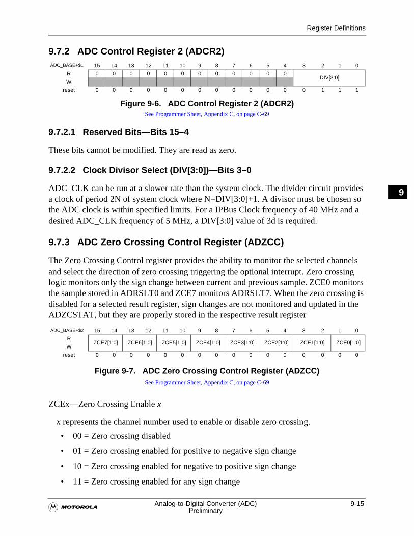
Register Definitions
�Analog-to-Digital Converter (ADC) 9-15
Preliminary
9
9.7.2 ADC Control Register 2 (ADCR2)
9.7.2.1 Reserved Bits—Bits 15–4
These bits cannot be modified. They are read as zero.
9.7.2.2 Clock Divisor Select (DIV[3:0])—Bits 3–0
ADC_CLK can be run at a slower rate than the system clock. The divider circuit provides a clock of period 2N of system clock where N=DIV[3:0]+1. A divisor must be chosen so the ADC clock is within specified limits. For a IPBus Clock frequency of 40 MHz and a desired ADC_CLK frequency of 5 MHz, a DIV[3:0] value of 3d is required.
9.7.3 ADC Zero Crossing Control Register (ADZCC)
The Zero Crossing Control register provides the ability to monitor the selected channels and select the direction of zero crossing triggering the optional interrupt. Zero crossing logic monitors only the sign change between current and previous sample. ZCE0 monitors the sample stored in ADRSLT0 and ZCE7 monitors ADRSLT7. When the zero crossing is disabled for a selected result register, sign changes are not monitored and updated in the ADZCSTAT, but they are properly stored in the respective result register
Figure 9-7. ADC Zero Crossing Control Register (ADZCC)See Programmer Sheet, Appendix C, on page C-69
ZCEx—Zero Crossing Enable x
x represents the channel number used to enable or disable zero crossing.
• 00 = Zero crossing disabled
• 01 = Zero crossing enabled for positive to negative sign change
• 10 = Zero crossing enabled for negative to positive sign change
• 11 = Zero crossing enabled for any sign change
ADC_BASE+$1 15 14 13 12 11 10 9 8 7 6 5 4 3 2 1 0
R 0 0 0 0 0 0 0 0 0 0 0 0DIV[3:0]
W
reset 0 0 0 0 0 0 0 0 0 0 0 0 0 1 1 1
Figure 9-6. ADC Control Register 2 (ADCR2)See Programmer Sheet, Appendix C, on page C-69
ADC_BASE+$2 15 14 13 12 11 10 9 8 7 6 5 4 3 2 1 0
RZCE7[1:0] ZCE6[1:0] ZCE5[1:0] ZCE4[1:0] ZCE3[1:0] ZCE2[1:0] ZCE1[1:0] ZCE0[1:0]
W
reset 0 0 0 0 0 0 0 0 0 0 0 0 0 0 0 0
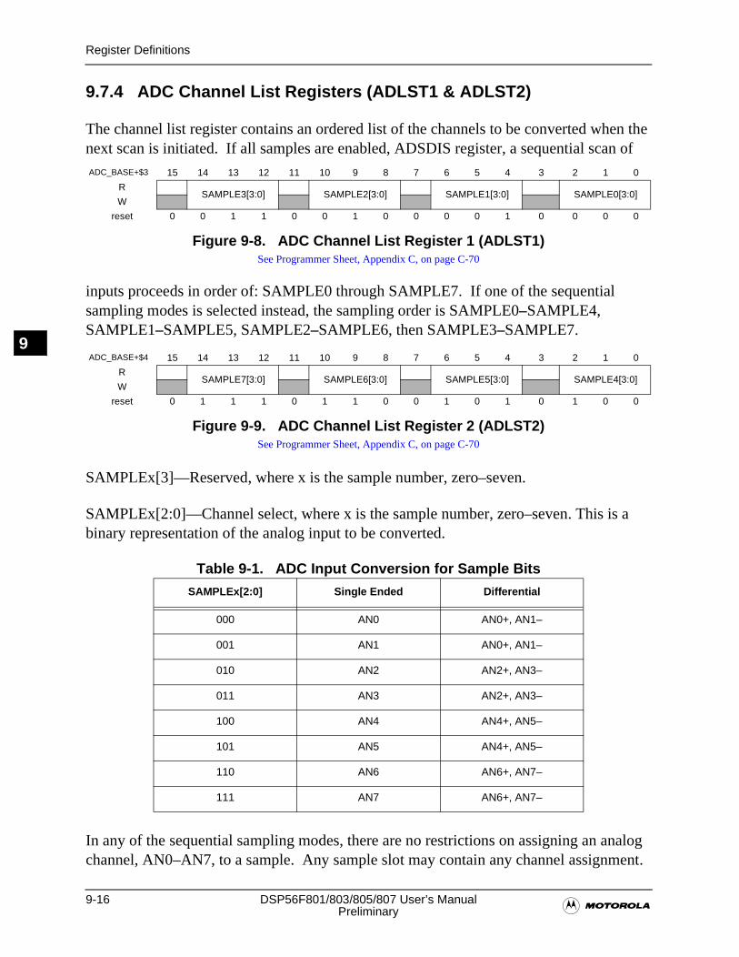
9-16 DSP56F801/803/805/807 User’s Manual�Preliminary
Register Definitions
9
9.7.4 ADC Channel List Registers (ADLST1 & ADLST2)
The channel list register contains an ordered list of the channels to be converted when the next scan is initiated. If all samples are enabled, ADSDIS register, a sequential scan of
inputs proceeds in order of: SAMPLE0 through SAMPLE7. If one of the sequential sampling modes is selected instead, the sampling order is SAMPLE0–SAMPLE4, SAMPLE1–SAMPLE5, SAMPLE2–SAMPLE6, then SAMPLE3–SAMPLE7.
SAMPLEx[3]—Reserved, where x is the sample number, zero–seven.
SAMPLEx[2:0]—Channel select, where x is the sample number, zero–seven. This is a binary representation of the analog input to be converted.
Table 9-1. ADC Input Conversion for Sample Bits
In any of the sequential sampling modes, there are no restrictions on assigning an analog channel, AN0–AN7, to a sample. Any sample slot may contain any channel assignment.
ADC_BASE+$3 15 14 13 12 11 10 9 8 7 6 5 4 3 2 1 0
RSAMPLE3[3:0] SAMPLE2[3:0] SAMPLE1[3:0] SAMPLE0[3:0]
W
reset 0 0 1 1 0 0 1 0 0 0 0 1 0 0 0 0
Figure 9-8. ADC Channel List Register 1 (ADLST1)See Programmer Sheet, Appendix C, on page C-70
ADC_BASE+$4 15 14 13 12 11 10 9 8 7 6 5 4 3 2 1 0
RSAMPLE7[3:0] SAMPLE6[3:0] SAMPLE5[3:0] SAMPLE4[3:0]
W
reset 0 1 1 1 0 1 1 0 0 1 0 1 0 1 0 0
Figure 9-9. ADC Channel List Register 2 (ADLST2)See Programmer Sheet, Appendix C, on page C-70
SAMPLEx[2:0] Single Ended Differential
000 AN0 AN0+, AN1–
001 AN1 AN0+, AN1–
010 AN2 AN2+, AN3–
011 AN3 AN2+, AN3–
100 AN4 AN4+, AN5–
101 AN5 AN4+, AN5–
110 AN6 AN6+, AN7–
111 AN7 AN6+, AN7–
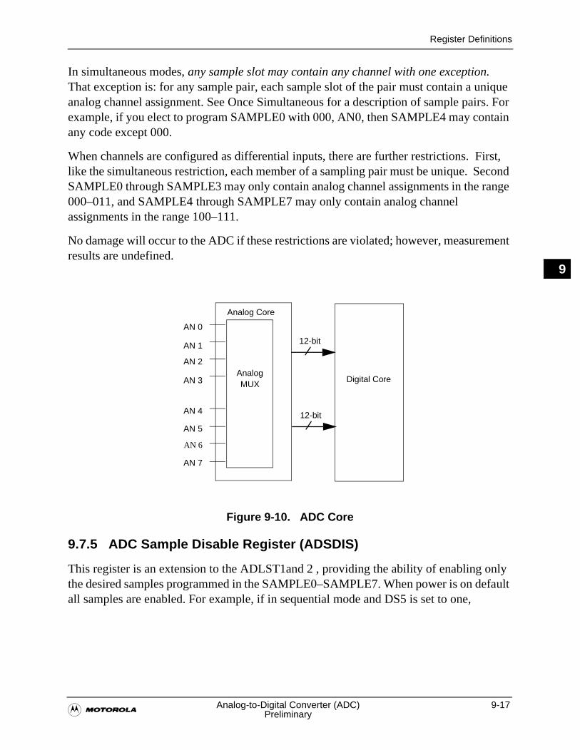
Register Definitions
�Analog-to-Digital Converter (ADC) 9-17
Preliminary
9
In simultaneous modes, any sample slot may contain any channel with one exception. That exception is: for any sample pair, each sample slot of the pair must contain a unique analog channel assignment. See Once Simultaneous for a description of sample pairs. For example, if you elect to program SAMPLE0 with 000, AN0, then SAMPLE4 may contain any code except 000.
When channels are configured as differential inputs, there are further restrictions. First, like the simultaneous restriction, each member of a sampling pair must be unique. Second SAMPLE0 through SAMPLE3 may only contain analog channel assignments in the range 000–011, and SAMPLE4 through SAMPLE7 may only contain analog channel assignments in the range 100–111.
No damage will occur to the ADC if these restrictions are violated; however, measurement results are undefined.
Figure 9-10. ADC Core
9.7.5 ADC Sample Disable Register (ADSDIS)
This register is an extension to the ADLST1and 2 , providing the ability of enabling only the desired samples programmed in the SAMPLE0–SAMPLE7. When power is on default all samples are enabled. For example, if in sequential mode and DS5 is set to one,
AN 0
AN 1
AN 2
AN 3
AN 4
AN 5
AN 6
AN 7
Analog Core
AnalogMUX
Digital Core
12-bit
12-bit
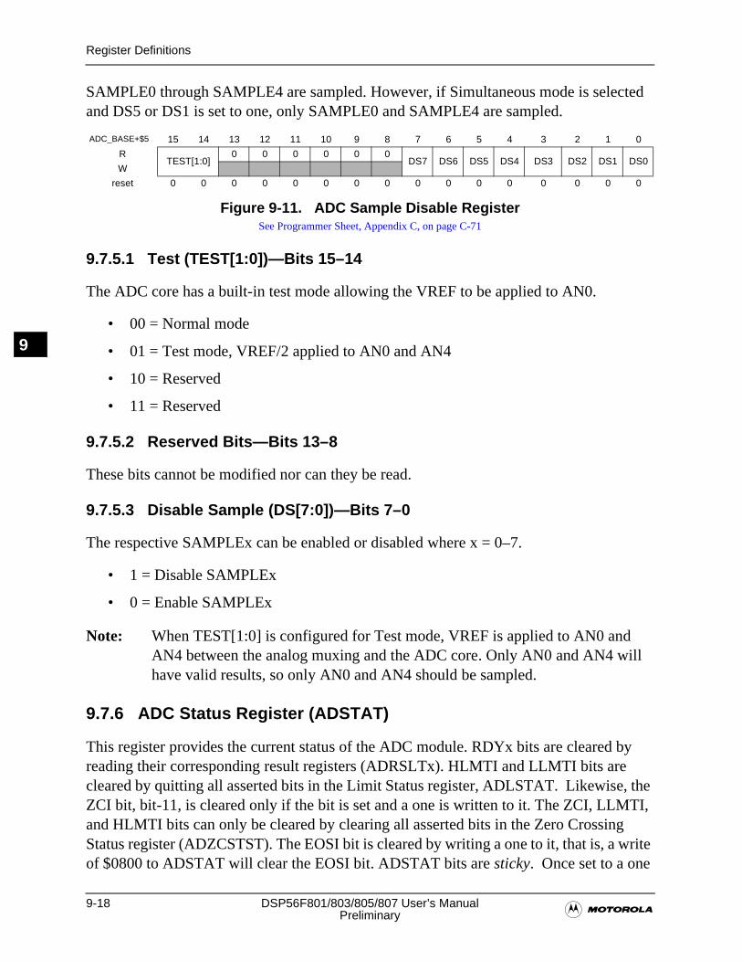
9-18 DSP56F801/803/805/807 User’s Manual�Preliminary
Register Definitions
9
SAMPLE0 through SAMPLE4 are sampled. However, if Simultaneous mode is selected and DS5 or DS1 is set to one, only SAMPLE0 and SAMPLE4 are sampled.
9.7.5.1 Test (TEST[1:0])—Bits 15–14
The ADC core has a built-in test mode allowing the VREF to be applied to AN0.
• 00 = Normal mode
• 01 = Test mode, VREF/2 applied to AN0 and AN4
• 10 = Reserved
• 11 = Reserved
9.7.5.2 Reserved Bits—Bits 13–8
These bits cannot be modified nor can they be read.
9.7.5.3 Disable Sample (DS[7:0])—Bits 7–0
The respective SAMPLEx can be enabled or disabled where x = 0–7.
• 1 = Disable SAMPLEx
• 0 = Enable SAMPLEx
Note: When TEST[1:0] is configured for Test mode, VREF is applied to AN0 and AN4 between the analog muxing and the ADC core. Only AN0 and AN4 will have valid results, so only AN0 and AN4 should be sampled.
9.7.6 ADC Status Register (ADSTAT)
This register provides the current status of the ADC module. RDYx bits are cleared by reading their corresponding result registers (ADRSLTx). HLMTI and LLMTI bits are cleared by quitting all asserted bits in the Limit Status register, ADLSTAT. Likewise, the ZCI bit, bit-11, is cleared only if the bit is set and a one is written to it. The ZCI, LLMTI, and HLMTI bits can only be cleared by clearing all asserted bits in the Zero Crossing Status register (ADZCSTST). The EOSI bit is cleared by writing a one to it, that is, a write of $0800 to ADSTAT will clear the EOSI bit. ADSTAT bits are sticky. Once set to a one
ADC_BASE+$5 15 14 13 12 11 10 9 8 7 6 5 4 3 2 1 0
RTEST[1:0]
0 0 0 0 0 0DS7 DS6 DS5 DS4 DS3 DS2 DS1 DS0
W
reset 0 0 0 0 0 0 0 0 0 0 0 0 0 0 0 0
Figure 9-11. ADC Sample Disable RegisterSee Programmer Sheet, Appendix C, on page C-71
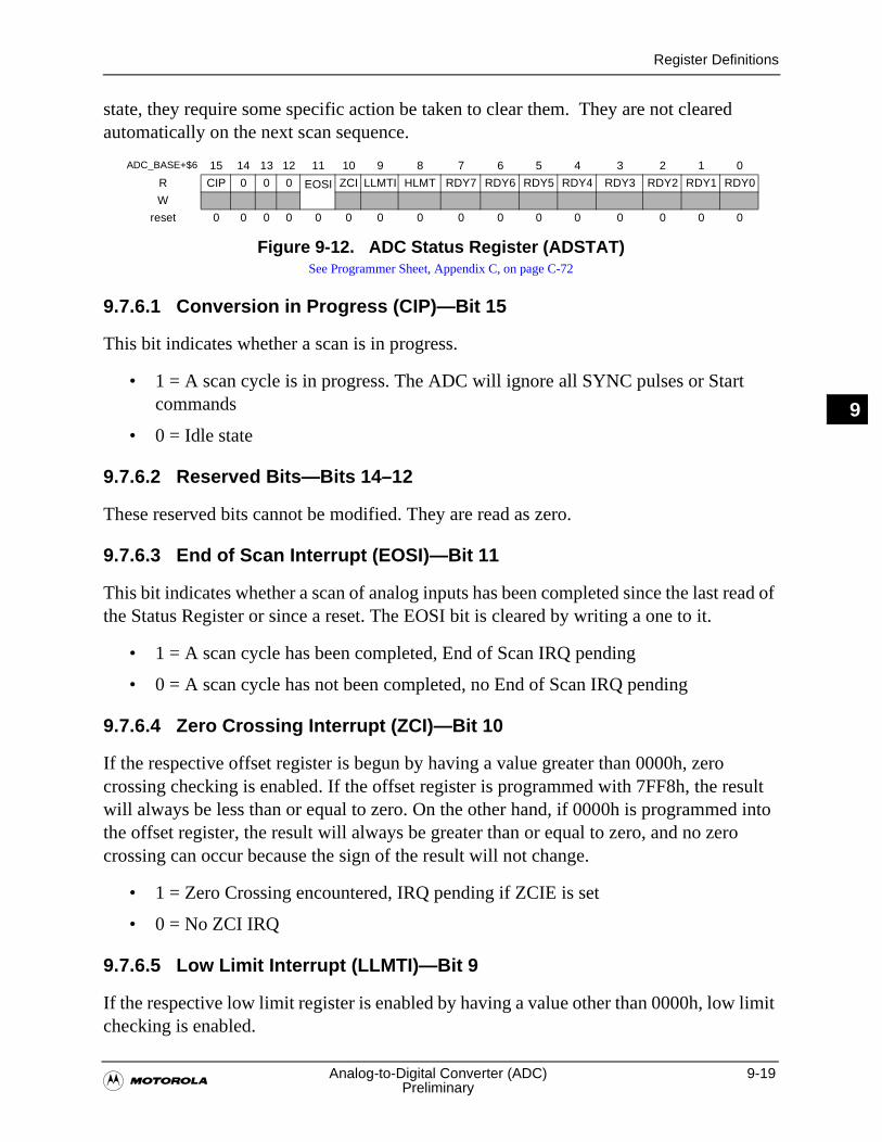
Register Definitions
�Analog-to-Digital Converter (ADC) 9-19
Preliminary
9
state, they require some specific action be taken to clear them. They are not cleared automatically on the next scan sequence.
9.7.6.1 Conversion in Progress (CIP)—Bit 15
This bit indicates whether a scan is in progress.
• 1 = A scan cycle is in progress. The ADC will ignore all SYNC pulses or Start commands
• 0 = Idle state
9.7.6.2 Reserved Bits—Bits 14–12
These reserved bits cannot be modified. They are read as zero.
9.7.6.3 End of Scan Interrupt (EOSI)—Bit 11
This bit indicates whether a scan of analog inputs has been completed since the last read of the Status Register or since a reset. The EOSI bit is cleared by writing a one to it.
• 1 = A scan cycle has been completed, End of Scan IRQ pending
• 0 = A scan cycle has not been completed, no End of Scan IRQ pending
9.7.6.4 Zero Crossing Interrupt (ZCI)—Bit 10
If the respective offset register is begun by having a value greater than 0000h, zero crossing checking is enabled. If the offset register is programmed with 7FF8h, the result will always be less than or equal to zero. On the other hand, if 0000h is programmed into the offset register, the result will always be greater than or equal to zero, and no zero crossing can occur because the sign of the result will not change.
• 1 = Zero Crossing encountered, IRQ pending if ZCIE is set
• 0 = No ZCI IRQ
9.7.6.5 Low Limit Interrupt (LLMTI)—Bit 9
If the respective low limit register is enabled by having a value other than 0000h, low limit checking is enabled.
ADC_BASE+$6 15 14 13 12 11 10 9 8 7 6 5 4 3 2 1 0
R CIP 0 0 0 EOSI
ZCI LLMTI HLMT RDY7 RDY6 RDY5 RDY4 RDY3 RDY2 RDY1 RDY0
W
reset 0 0 0 0 0 0 0 0 0 0 0 0 0 0 0 0
Figure 9-12. ADC Status Register (ADSTAT)See Programmer Sheet, Appendix C, on page C-72
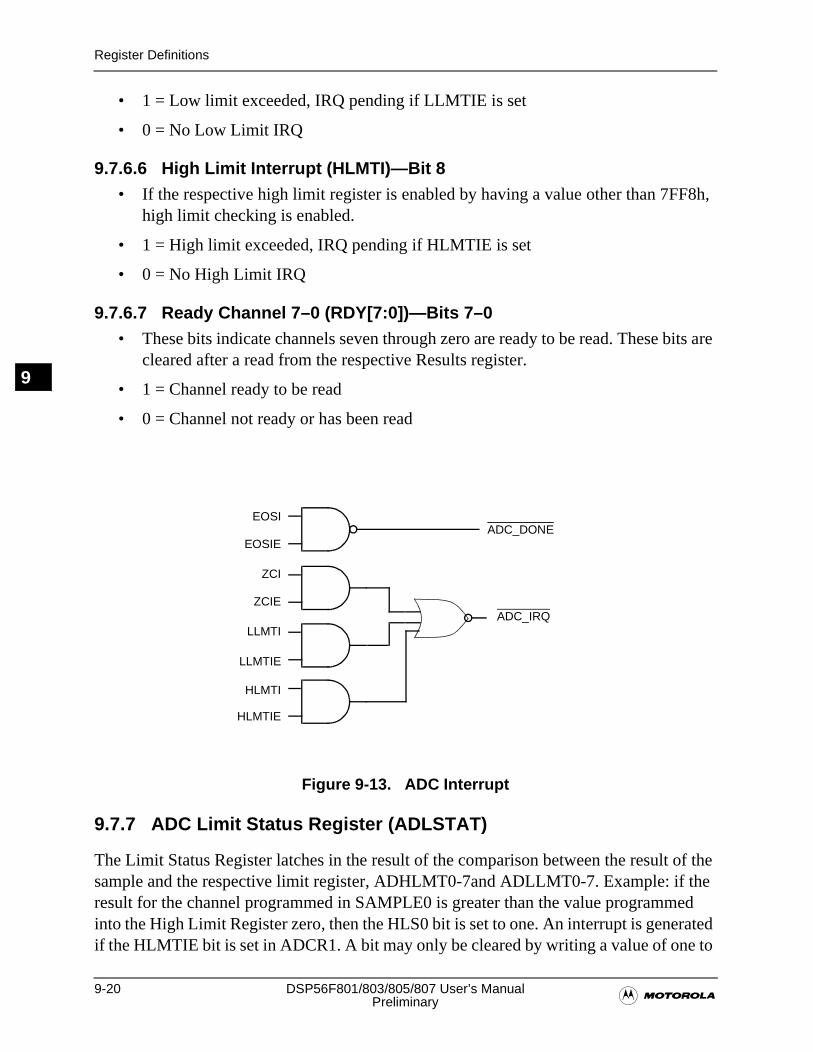
9-20 DSP56F801/803/805/807 User’s Manual�Preliminary
Register Definitions
9
• 1 = Low limit exceeded, IRQ pending if LLMTIE is set
• 0 = No Low Limit IRQ
9.7.6.6 High Limit Interrupt (HLMTI)—Bit 8• If the respective high limit register is enabled by having a value other than 7FF8h,
high limit checking is enabled.
• 1 = High limit exceeded, IRQ pending if HLMTIE is set
• 0 = No High Limit IRQ
9.7.6.7 Ready Channel 7–0 (RDY[7:0])—Bits 7–0• These bits indicate channels seven through zero are ready to be read. These bits are
cleared after a read from the respective Results register.
• 1 = Channel ready to be read
• 0 = Channel not ready or has been read
Figure 9-13. ADC Interrupt
9.7.7 ADC Limit Status Register (ADLSTAT)
The Limit Status Register latches in the result of the comparison between the result of the sample and the respective limit register, ADHLMT0-7and ADLLMT0-7. Example: if the result for the channel programmed in SAMPLE0 is greater than the value programmed into the High Limit Register zero, then the HLS0 bit is set to one. An interrupt is generated if the HLMTIE bit is set in ADCR1. A bit may only be cleared by writing a value of one to
EOSI
EOSIE
ZCI
ZCIE
LLMTI
LLMTIE
HLMTI
HLMTIE
ADC_IRQ
ADC_DONE

Register Definitions
�Analog-to-Digital Converter (ADC) 9-21
Preliminary
9
that specific bit. These bits are sticky. Once set, the bits require a specific modification to clear them. They are not cleared automatically by subsequent conversions.
9.7.8 ADC Zero Crossing Status Register (ADZCSTAT)
The Zero Crossing Status Register latches in the result of the comparison between the current result of the sample and the previous result of the same sample register. For example, if the result for the channel programmed in SAMPLE0 changes sign from the previous conversion and the respective ZCE bit in register ADZCC is set to 11b, any edge change, then the ZCS0 bit is set to one. An interrupt is generated if the ZCIE bit is set in ADCR1. A bit can only be cleared by writing a value of one to that specific bit. These bits are sticky. Once set, they require a write to clear them. They are not cleared automatically by subsequent conversions..
9.7.8.1 Reserved Bits—Bits 15–8
These reserved bits may not be modified. They are read as zero.
9.7.8.2 Zero Crossing Status (ZCS[7:0])—Bits 7–0
• 0 = a. A sign change did not occur in a comparison between the current channelx result and the previous channelx result, or
b. Zero Crossing Control is disabled for channelx in the Zero Crossing Control Register, ADZCC
• 1 = In a comparison between the current channelx result and the previous channelx result, a sign change condition occurred as defined in the Zero Crossing Control Register (ADZCC)
Note: To clear a specific ZCS[7:0] bit, write a value of one to that specific bit.
ADC_BASE+$7 15 14 13 12 11 10 9 8 7 6 5 4 3 2 1 0
RHLS7 HLS6 HLS5 HLS4 HLS3 HLS2 HLS1 HLS0 LLS7 LLS6 LLS5 LLS4 LLS3 LLS2 LLS1 LLS0
W
reset 0 0 0 0 0 0 0 0 0 0 0 0 0 0 0 0
Figure 9-14. ADC Limit Status Register (ADLSTAT)See Programmer Sheet, Appendix C, on page C-73
ADC_BASE+$8 15 14 13 12 11 10 9 8 7 6 5 4 3 2 1 0
R 0 0 0 0 0 0 0 0ZCS7 ZCS6 ZCS5 ZCS4 ZCS3 ZCS2 ZCS1 ZCS0
W
reset 0 0 0 0 0 0 0 0 0 0 0 0 0 0 0 0
Figure 9-15. ADC Zero Crossing Status Register (ADZCSTAT)See Programmer Sheet, Appendix C, on page C-74
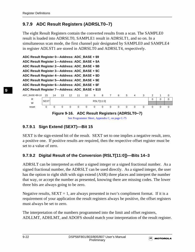
9-22 DSP56F801/803/805/807 User’s Manual�Preliminary
Register Definitions
9
9.7.9 ADC Result Registers (ADRSLT0–7)
The eight Result Registers contain the converted results from a scan. The SAMPLE0 result is loaded into ADRSLT0, SAMPLE1 result in ADRSLT1, and so on. In a simultaneous scan mode, the first channel pair designated by SAMPLE0 and SAMPLE4 in register ADLST1 are stored in ADRSLT0 and ADRSLT4, respectively.
ADC Result Register 0—Address: ADC_BASE + $9ADC Result Register 1—Address: ADC_BASE + $AADC Result Register 2—Address: ADC_BASE + $BADC Result Register 3—Address: ADC_BASE + $CADC Result Register 4—Address: ADC_BASE + $DADC Result Register 5—Address: ADC_BASE + $EADC Result Register 6—Address: ADC_BASE + $FADC Result Register 7—Address: ADC_BASE + $10
9.7.9.1 Sign Extend (SEXT)—Bit 15
SEXT is the sign-extend bit of the result. SEXT set to one implies a negative result, zero, a positive one. If positive results are required, then the respective offset register must be set to a value of zero.
9.7.9.2 Digital Result of the Conversion (RSLT[11:0])—Bits 14–3
ADRSLT can be interpreted as either a signed integer or a signed fractional number. As a signed fractional number, the ADRSLT can be used directly. As a signed integer, the user has the option to right shift with sign extend (ASR) three places and interpret the number that way, or accept the number as presented, knowing there are missing codes. The lower three bits are always going to be zero.
Negative results, SEXT = 1, are always presented in two’s compliment format. If it is a requirement of your application the result registers always be positive, the offset registers must always be set to zero.
The interpretation of the numbers programmed into the limit and offset registers, ADLLMT, ADHLMT, and ADOFS should match your interpretation of the result register.
ADC_BASE+$9-10 15 14 13 12 11 10 9 8 7 6 5 4 3 2 1 0
RSEXT RSLT[11:0]
0 0 0
W
reset 0 0 0 0 0 0 0 0 0 0 0 0 0 0 0 0
Figure 9-16. ADC Result Registers (ADRSLT0–7)See Programmer Sheet, Appendix C, on page C-75
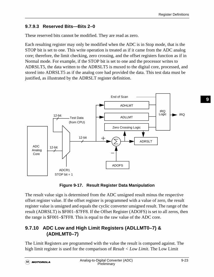
Register Definitions
�Analog-to-Digital Converter (ADC) 9-23
Preliminary
9
9.7.9.3 Reserved Bits—Bits 2–0
These reserved bits cannot be modified. They are read as zero.
Each resulting register may only be modified when the ADC is in Stop mode, that is the STOP bit is set to one. This write operation is treated as if it came from the ADC analog core; therefore, the limit checking, zero crossing, and the offset registers function as if in Normal mode. For example, if the STOP bit is set to one and the processor writes to ADRSLT5, the data written to the ADRSLT5 is muxed to the digital core, processed, and stored into ADRSLT5 as if the analog core had provided the data. This test data must be justified, as illustrated by the ADRSLT register definition.
Figure 9-17. Result Register Data Manipulation
The result value sign is determined from the ADC unsigned result minus the respective offset register value. If the offset register is programmed with a value of zero, the result register value is unsigned and equals the cyclic converter unsigned result. The range of the result (ADRSLT) is $F001–$7FF8. If the Offset Register (ADOFS) is set to all zeros, then the range is $F001–$7FF8. This is equal to the raw value of the ADC core.
9.7.10 ADC Low and High Limit Registers (ADLLMT0–7) & (ADHLMT0–7)
The Limit Registers are programmed with the value the result is compared against. The high limit register is used for the comparison of Result < Low Limit. The Low Limit
ADCAnalogCore
12-bit
12-bit
12-bit
Test Data
ADOFS
ADRSLT
ADCR1STOP bit = 1
ADHLMT
ADLLMT
Zero Crossing Logic
IRQLogic IRQ
(from CPU)
End of Scan
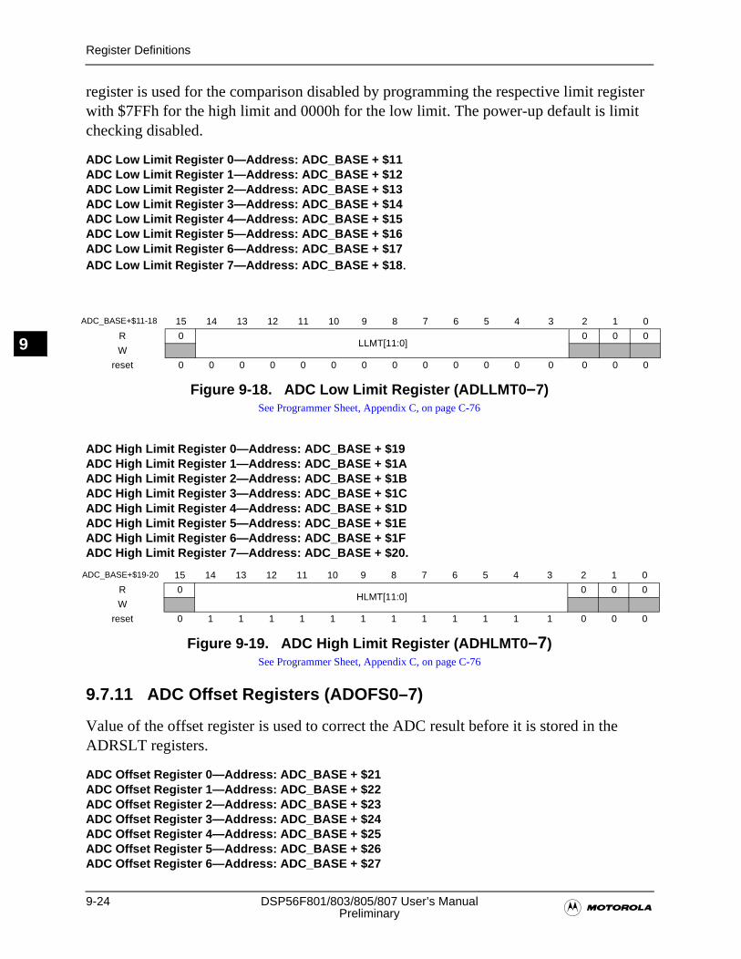
9-24 DSP56F801/803/805/807 User’s Manual�Preliminary
Register Definitions
9
register is used for the comparison disabled by programming the respective limit register with $7FFh for the high limit and 0000h for the low limit. The power-up default is limit checking disabled.
ADC Low Limit Register 0—Address: ADC_BASE + $11ADC Low Limit Register 1—Address: ADC_BASE + $12ADC Low Limit Register 2—Address: ADC_BASE + $13ADC Low Limit Register 3—Address: ADC_BASE + $14ADC Low Limit Register 4—Address: ADC_BASE + $15ADC Low Limit Register 5—Address: ADC_BASE + $16ADC Low Limit Register 6—Address: ADC_BASE + $17ADC Low Limit Register 7—Address: ADC_BASE + $18 .
ADC High Limit Register 0—Address: ADC_BASE + $19ADC High Limit Register 1—Address: ADC_BASE + $1AADC High Limit Register 2—Address: ADC_BASE + $1BADC High Limit Register 3—Address: ADC_BASE + $1CADC High Limit Register 4—Address: ADC_BASE + $1DADC High Limit Register 5—Address: ADC_BASE + $1EADC High Limit Register 6—Address: ADC_BASE + $1FADC High Limit Register 7—Address: ADC_BASE + $20.
9.7.11 ADC Offset Registers (ADOFS0–7)
Value of the offset register is used to correct the ADC result before it is stored in the ADRSLT registers.
ADC Offset Register 0—Address: ADC_BASE + $21ADC Offset Register 1—Address: ADC_BASE + $22ADC Offset Register 2—Address: ADC_BASE + $23ADC Offset Register 3—Address: ADC_BASE + $24ADC Offset Register 4—Address: ADC_BASE + $25ADC Offset Register 5—Address: ADC_BASE + $26ADC Offset Register 6—Address: ADC_BASE + $27
ADC_BASE+$11-18 15 14 13 12 11 10 9 8 7 6 5 4 3 2 1 0
R 0LLMT[11:0]
0 0 0
W
reset 0 0 0 0 0 0 0 0 0 0 0 0 0 0 0 0
Figure 9-18. ADC Low Limit Register (ADLLMT0–7)See Programmer Sheet, Appendix C, on page C-76
ADC_BASE+$19-20 15 14 13 12 11 10 9 8 7 6 5 4 3 2 1 0
R 0HLMT[11:0]
0 0 0
W
reset 0 1 1 1 1 1 1 1 1 1 1 1 1 0 0 0
Figure 9-19. ADC High Limit Register (ADHLMT0–7)See Programmer Sheet, Appendix C, on page C-76
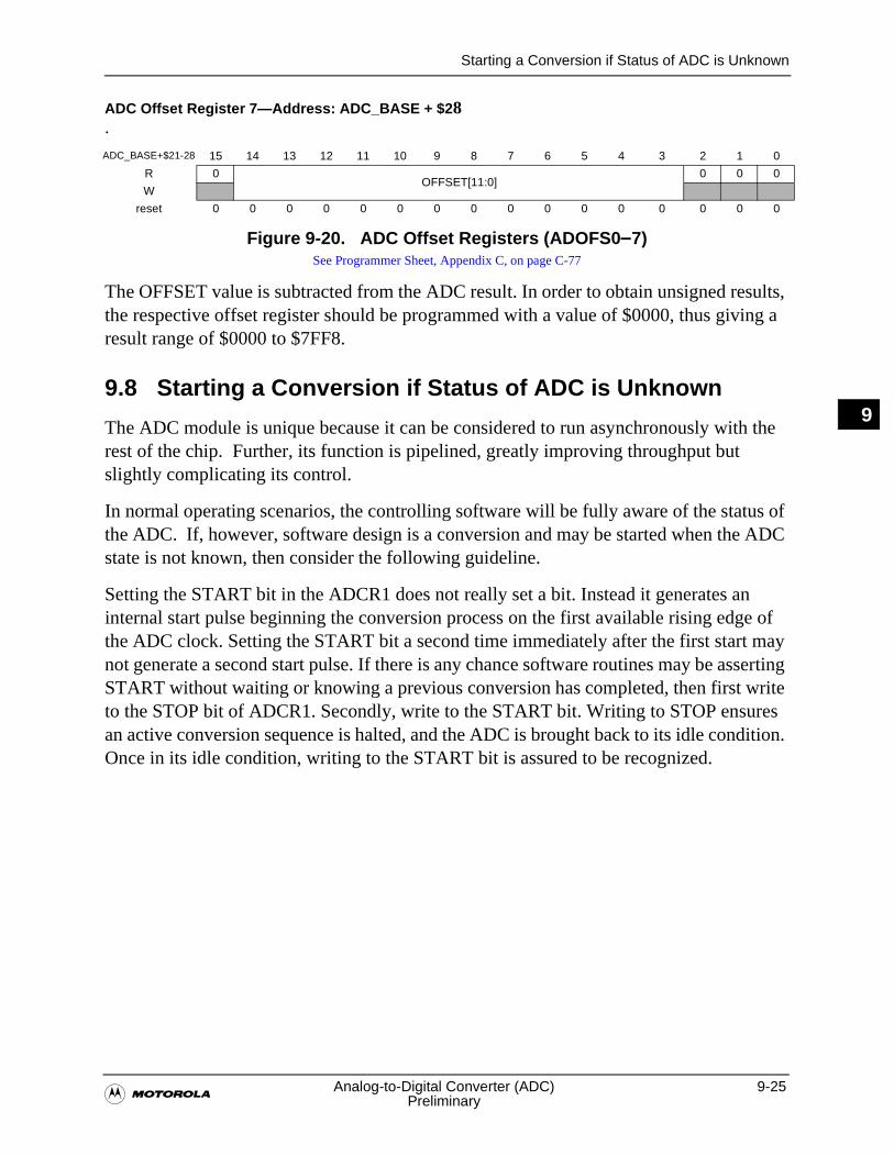
Starting a Conversion if Status of ADC is Unknown
�Analog-to-Digital Converter (ADC) 9-25
Preliminary
9
ADC Offset Register 7—Address: ADC_BASE + $2 8.
The OFFSET value is subtracted from the ADC result. In order to obtain unsigned results, the respective offset register should be programmed with a value of $0000, thus giving a result range of $0000 to $7FF8.
9.8 Starting a Conversion if Status of ADC is Unknown
The ADC module is unique because it can be considered to run asynchronously with the rest of the chip. Further, its function is pipelined, greatly improving throughput but slightly complicating its control.
In normal operating scenarios, the controlling software will be fully aware of the status of the ADC. If, however, software design is a conversion and may be started when the ADC state is not known, then consider the following guideline.
Setting the START bit in the ADCR1 does not really set a bit. Instead it generates an internal start pulse beginning the conversion process on the first available rising edge of the ADC clock. Setting the START bit a second time immediately after the first start may not generate a second start pulse. If there is any chance software routines may be asserting START without waiting or knowing a previous conversion has completed, then first write to the STOP bit of ADCR1. Secondly, write to the START bit. Writing to STOP ensures an active conversion sequence is halted, and the ADC is brought back to its idle condition. Once in its idle condition, writing to the START bit is assured to be recognized.
ADC_BASE+$21-28 15 14 13 12 11 10 9 8 7 6 5 4 3 2 1 0
R 0OFFSET[11:0]
0 0 0
W
reset 0 0 0 0 0 0 0 0 0 0 0 0 0 0 0 0
Figure 9-20. ADC Offset Registers (ADOFS0–7)See Programmer Sheet, Appendix C, on page C-77
9-26 DSP56F801/803/805/807 User’s Manual�Preliminary
Starting a Conversion if Status of ADC is Unknown
9
�Quadrature Decoder 10-1
Preliminary
10
Chapter 10Quadrature Decoder

10-2 DSP56F801/803/805/807 User’s Manual�Preliminary
10
Pin Descriptions
�Quadrature Decoder 10-3
Preliminary
10
10.1 Introduction
Each Quadrature Decoder module has four input signals and circuitry called the switch matrix and has three modes. It provides a means to share input pins with an associated time module.
Quadrature Decoder refers to the module on the DSP56F801/803/805/807 and an external device mounted on a motor shaft.
The DSP56F801 does not have a Quadrature Decoder
The DSP56F803 has one Quadrature Decoder
The DSP56F805/807 have two Quadrature Decoders
On the DSP56F801/803/805/807, the Quad Timer modules A and B share pins with Quadrature Decoder modules number zero and number one. If the shared pins are not configured as timer outputs, then the pins are available for use as inputs to the Quadrature Decoder modules. Each Quadrature Decoder module has four input signals: PHASEA, PHASEB, INDEX, and HOME.
10.2 Features• Includes logic to decode quadrature signals
• Configurable digital filter for inputs
• 32-bit position counter
• 16-bit position difference register
• Maximum count frequency equals the peripheral clock rate
• Position counter can be initialized by SW or external events
• Preloadable 16-bit revolution counter
• Inputs can be connected to a general purpose timer to aid low speed velocity measurements
• Quadrature decoder filter can be bypassed
• A watchdog timer to detect a non-rotating shaft condition
10.3 Pin Descriptions
With the DSP56F803, input pins are labeled PHASEA0, PHASEB0, INDEX0 and HOME0. On the DSP56F805/807, they are PHASEA0, PHASEB0, INDEX0, HOME0, PHASEA1, PHASEB1, INDEX1 and HOME1.
10-4 DSP56F801/803/805/807 User’s Manual�Preliminary
Pin Descriptions
10
10.3.1 Phase A Input (PHASEA)
The PHASEA input can be connected to one of the phases from a two-phase shaft Quadrature Encoder output. It is used by the Quadrature Decoder module in conjunction with the PHASEB input to indicate a decoder increment has passed, and to calculate its direction. PHASEA is the leading phase for a shaft rotating in the positive direction. PHASEA is the trailing phase for a shaft rotating in the negative direction. It can also be used as the single input when the Quadrature Decoder module is used as a single phase pulse accumulator.
The PHASEA input is also an input capture channel for one of the timer modules. The exact connection to the timer module is specified in Table 10-1.
10.3.2 Phase B Input (PHASEB)
The PHASEB input is used as one of the phases from a two phase shaft Quadrature Encoder output. It is used by the Quadrature Decoder module in conjunction with the PHASEA input indicating a decoder increment has passed, and to calculate its direction. PHASEB is the trailing phase for a shaft rotating in the positive direction. PHASEB is the leading phase for a shaft rotating in the negative direction.
The PHASEB input is also an input capture channel for one of the timer modules. The exact connection to the timer module is specified in Table 10-1.
10.3.3 Index Input (INDEX)
Normally connected to the index pulse output of a Quadrature Encoder, this pulse can optionally reset the position counter and the pulse accumulator of the Quadrature Decoder module. It also causes a change of state on the revolution counter. The direction of this change, increment or decrement, is calculated from the PHASEA and PHASEB inputs.
The INDEX input is also an input capture channel for one of the timer modules. The exact connection to the timer module is specified in Table 10-1.
10.3.4 Home Switch Input (HOME)
The HOME input can be used by the Quadrature Decoder and the Timer Module. This input can be used to trigger the initialization of the position counters (UPOS and LPOS). Often this signal is connected to a sensor signaling the motor or machine notifying it has reached a defined home position. This general purpose signal is also connected to the timer module as specified in Table 10-1.
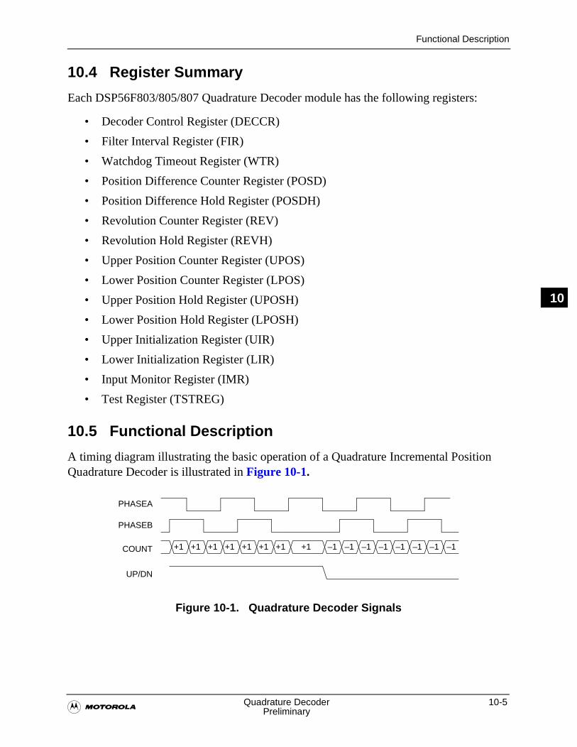
Functional Description
�Quadrature Decoder 10-5
Preliminary
10
10.4 Register Summary
Each DSP56F803/805/807 Quadrature Decoder module has the following registers:
• Decoder Control Register (DECCR)
• Filter Interval Register (FIR)
• Watchdog Timeout Register (WTR)
• Position Difference Counter Register (POSD)
• Position Difference Hold Register (POSDH)
• Revolution Counter Register (REV)
• Revolution Hold Register (REVH)
• Upper Position Counter Register (UPOS)
• Lower Position Counter Register (LPOS)
• Upper Position Hold Register (UPOSH)
• Lower Position Hold Register (LPOSH)
• Upper Initialization Register (UIR)
• Lower Initialization Register (LIR)
• Input Monitor Register (IMR)
• Test Register (TSTREG)
10.5 Functional Description
A timing diagram illustrating the basic operation of a Quadrature Incremental Position Quadrature Decoder is illustrated in Figure 10-1.
Figure 10-1. Quadrature Decoder Signals
+1 +1 +1 +1 +1 +1 +1 +1 –1 –1 –1 –1 –1 –1 –1 –1
PHASEB
COUNT
UP/DN
PHASEA
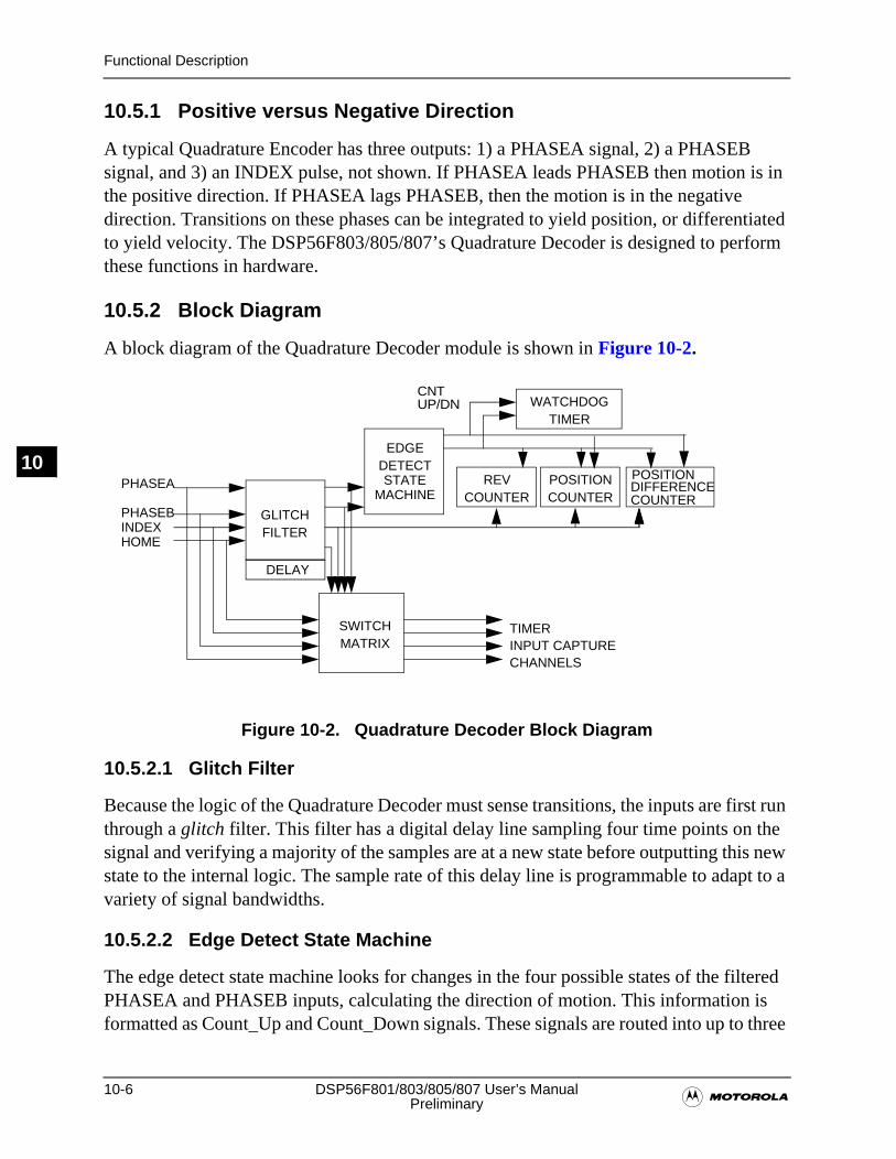
10-6 DSP56F801/803/805/807 User’s Manual�Preliminary
Functional Description
10
10.5.1 Positive versus Negative Direction
A typical Quadrature Encoder has three outputs: 1) a PHASEA signal, 2) a PHASEB signal, and 3) an INDEX pulse, not shown. If PHASEA leads PHASEB then motion is in the positive direction. If PHASEA lags PHASEB, then the motion is in the negative direction. Transitions on these phases can be integrated to yield position, or differentiated to yield velocity. The DSP56F803/805/807’s Quadrature Decoder is designed to perform these functions in hardware.
10.5.2 Block Diagram
A block diagram of the Quadrature Decoder module is shown in Figure 10-2.
Figure 10-2. Quadrature Decoder Block Diagram
10.5.2.1 Glitch Filter
Because the logic of the Quadrature Decoder must sense transitions, the inputs are first run through a glitch filter. This filter has a digital delay line sampling four time points on the signal and verifying a majority of the samples are at a new state before outputting this new state to the internal logic. The sample rate of this delay line is programmable to adapt to a variety of signal bandwidths.
10.5.2.2 Edge Detect State Machine
The edge detect state machine looks for changes in the four possible states of the filtered PHASEA and PHASEB inputs, calculating the direction of motion. This information is formatted as Count_Up and Count_Down signals. These signals are routed into up to three
GLITCHFILTER
EDGEDETECTSTATE
MACHINE
WATCHDOGTIMER
DELAY
REVCOUNTER
POSITIONCOUNTER
SWITCHMATRIX
CNTUP/DN
TIMERINPUT CAPTURECHANNELS
POSITIONDIFFERENCECOUNTER
PHASEA
PHASEBINDEXHOME
Functional Description
�Quadrature Decoder 10-7
Preliminary
10
up/down counters: 1) a position counter, 2) a revolution counter, and 3) a position difference counter.
10.5.2.3 Position Counter
The 32-bit position counter calculates up or down on every count pulse, generated by the difference of PHASEA and PHASEB. This counter acts as an integrator, whose count value is proportional to position. The direction of the count is determined by the Count Up and Count Down signals. Position counters may be initialized to a predetermined value by one of three different methods: 1) software-triggered event, 2) INDEX signal transition, or 3) a HOME signal transition. The INDEX and HOME signals can be programmed to interrupt the processor. Whenever the position counter is read, either UPOS or LPOS, a snapshot of the position counter, the position difference counter, and the revolution counters are each placed into their respective Hold registers. The direction of the count is determined by Count_Up and Count_Down signals.
10.5.2.4 Position Difference Counter
The 16-bit position difference counter contains the position difference value occurring between each read of the position register. This register counts up or down on every count pulse. The counter acts as a differentiator whose count value is proportional to the change in position since the last time the position counter was read. When the position register is read, the position difference of the counter’s contents are copied into the Position Difference Hold Register (POSDH) and position difference counter is cleared.
10.5.2.5 Position Difference Counter Hold
This register stores a copy of the position difference counter at the time the position register was read. When the position register is read, the position difference of the counter’s contents are copied into the Position Difference Hold Register (POSDH) and position difference counter is cleared.
10.5.2.6 Revolution Counter
The 16-bit up/down revolution counter is intended to count, or integrate revolutions. This is done by counting index pulses. The direction of the count is determined by the Count_Up and Count_Down signals, determined by Phase A& B inputs. If the direction of the count is different on the rising and falling edges of the index pulse, it indicates the Quadrature Encoder changed direction on the index pulse.
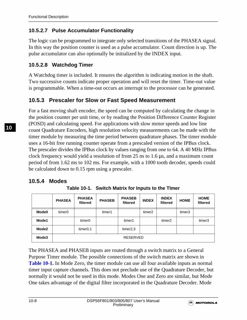
10-8 DSP56F801/803/805/807 User’s Manual�Preliminary
Functional Description
10
10.5.2.7 Pulse Accumulator Functionality
The logic can be programmed to integrate only selected transitions of the PHASEA signal. In this way the position counter is used as a pulse accumulator. Count direction is up. The pulse accumulator can also optionally be initialized by the INDEX input.
10.5.2.8 Watchdog Timer
A Watchdog timer is included. It ensures the algorithm is indicating motion in the shaft. Two successive counts indicate proper operation and will reset the timer. Time-out value is programmable. When a time-out occurs an interrupt to the processor can be generated.
10.5.3 Prescaler for Slow or Fast Speed Measurement
For a fast moving shaft encoder, the speed can be computed by calculating the change in the position counter per unit time, or by reading the Position Difference Counter Register (POSD) and calculating speed. For applications with slow motor speeds and low line count Quadrature Encoders, high resolution velocity measurements can be made with the timer module by measuring the time period between quadrature phases. The timer module uses a 16-bit free running counter operate from a prescaled version of the IPBus clock. The prescaler divides the IPBus clock by values ranging from one to 64. A 40 MHz IPBus clock frequency would yield a resolution of from 25 ns to 1.6 µs, and a maximum count period of from 1.62 ms to 102 ms. For example, with a 1000 tooth decoder, speeds could be calculated down to 0.15 rpm using a prescaler.
10.5.4 Modes
The PHASEA and PHASEB inputs are routed through a switch matrix to a General Purpose Timer module. The possible connections of the switch matrix are shown in Table 10-1. In Mode Zero, the timer module can use all four available inputs as normal timer input capture channels. This does not preclude use of the Quadrature Decoder, but normally it would not be used in this mode. Modes One and Zero are similar, but Mode One takes advantage of the digital filter incorporated in the Quadrature Decoder. Mode
Table 10-1. Switch Matrix for Inputs to the TImer
PHASEAPHASEAfiltered
PHASEBPHASEBfiltered
INDEXINDEXfiltered
HOMEHOMEfiltered
Mode0 timer0 timer1 timer2 timer3
Mode1 timer0 timer1 timer2 timer3
Mode2 timer0,1 timer2,3
Mode3 RESERVED
Register Definitions
�Quadrature Decoder 10-9
Preliminary
10
Two is the mode most likely to be used in conjunction with operation of the Quadrature Decoder. Both the positive and negative edges of PHASEA and PHASEB can be captured in Mode Two. The full speed range measurement is able to be reached in this mode.
10.6 Holding Registers and Initializing Registers
Hold registers are associated with 1) Position, 2) Position Difference, and 3) Revolution counters. When counter registers are read, a contents copy of the counter register is written to the corresponding hold register. Taking a snapshot of the counters’ values provides a consistent view of a system position and a velocity to be attained.
The counter and the hold registers are read/write capable. But beware of writing values into any hold register and then reading any counter. The results? The hold register contents will be overwritten with the values in the counters.
The Position counter is 32 bits wide. Assuring it can be reliably initialized with two 16-bit accesses, two registers, an upper and a lower initialization register, are provided. The Upper Initialization Register (UIR) and Lower Initialization Register (LIR) should be modified with the desired value. Next, the Position counter can be loaded by writing one to the SWIP bit in the Decoder Control Register (DECCR). Alternatively, either the XIP or the HIP bits in the DECCR can enable the Position counter to be initialized in response to a HOME or INDEX signal transition.
10.7 Register Definitions
The address of a register is the sum of a base address and an address offset. The base address is defined at the MCU level, while the address offset is defined at the module level Refer to Table 3-11. All memory locations base and offsets are given in hex.
Each of the following set of registers are used for each Quadrature Decoder Module. For example, if there are two Quadrature Decoders on the chip, there are two Decoder Control Registers: DEC0_DECCR at data memory location DEC0_BASE+$0 and DEC1_DECCR at data memory location DEC1_BASE+$0.
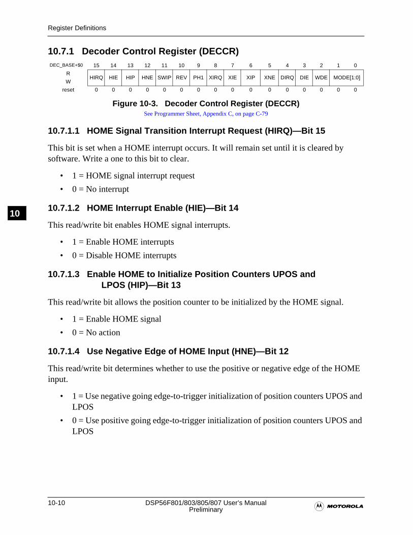
10-10 DSP56F801/803/805/807 User’s Manual�Preliminary
Register Definitions
10
10.7.1 Decoder Control Register (DECCR)
10.7.1.1 HOME Signal Transition Interrupt Request (HIRQ)—Bit 15
This bit is set when a HOME interrupt occurs. It will remain set until it is cleared by software. Write a one to this bit to clear.
• 1 = HOME signal interrupt request
• 0 = No interrupt
10.7.1.2 HOME Interrupt Enable (HIE)—Bit 14
This read/write bit enables HOME signal interrupts.
• 1 = Enable HOME interrupts
• 0 = Disable HOME interrupts
10.7.1.3 Enable HOME to Initialize Position Counters UPOS and LPOS (HIP)—Bit 13
This read/write bit allows the position counter to be initialized by the HOME signal.
• 1 = Enable HOME signal
• 0 = No action
10.7.1.4 Use Negative Edge of HOME Input (HNE)—Bit 12
This read/write bit determines whether to use the positive or negative edge of the HOME input.
• 1 = Use negative going edge-to-trigger initialization of position counters UPOS and LPOS
• 0 = Use positive going edge-to-trigger initialization of position counters UPOS and LPOS
DEC_BASE+$0 15 14 13 12 11 10 9 8 7 6 5 4 3 2 1 0
RHIRQ HIE HIP HNE SWIP REV PH1 XIRQ XIE XIP XNE DIRQ DIE WDE MODE[1:0]
W
reset 0 0 0 0 0 0 0 0 0 0 0 0 0 0 0 0
Figure 10-3. Decoder Control Register (DECCR)See Programmer Sheet, Appendix C, on page C-79
Register Definitions
�Quadrature Decoder 10-11
Preliminary
10
10.7.1.5 Software Triggered Initialization of Position Counters UPOS and LPOS (SWIP)—Bit 11
Writing a one to this bit will transfer the UIR and LIR contents to ENPOS. This bit is always read as a zero.
• 1 = Initialize position counter
• 0 = No action
10.7.1.6 Enable Reverse Direction Counting (REV)—Bit 10
This read/write bit reverses the interpretation of the quadrature signal, changing the direction of count.
• 1 = Count in the reverse direction
• 0 = Count normally
10.7.1.7 Enable Signal Phase Count Mode (PH1)—Bit 9
This read/write bit bypasses the Quadrature Decoder logic.
• 1 = Bypass the Quadrature Decoder. A positive transition of the PHASEA input generates a count signal. The PHASEB input and the REV bit control the counter direction
— IF REV = 0, PHASEB = 0, then count up
— IF REV = 0, PHASEB = 1, then count down
— IF REV = 1, PHASEB = 0, then count down
— IF REV = 1, PHASEB = 1, then count up
• 0 = Use standard Quadrature Decoder where PHASEA and PHASEB represent a two phase quadrature signal
10.7.1.8 Index Pulse Interrupt Request (XIRQ)—Bit 8
This bit is set when an index interrupt occurs. It will remain set until cleared by software. The clearing procedure is to write a one to this bit.
• 1 = Index pulse interrupt has occurred
• 0 = No interrupt has occurred
10.7.1.9 Index Pulse Interrupt Enable (XIE)—Bit 7
This read/write bit enables index interrupts.
10-12 DSP56F801/803/805/807 User’s Manual�Preliminary
Register Definitions
10
• 1= Index pulse interrupt is enabled
• 0= Index pulse interrupt is disabled
10.7.1.10 Index Triggered Initialization of Position Counters UPOS and LPOS (XIP)—Bit 6
This read/write bit enables the position counter to be initialized by the INDEX pulse.
• 1 = INDEX pulse initializes the position counter
• 0 = No action
10.7.1.11 Use Negative Edge of Index Pulse (XNE)—Bit 5
This read/write bit determines the edge of the index pulse used to initialize the position counter.
• 1 = Use negative transition edge of INDEX pulse
• 0 = Use positive transition edge of INDEX pulse
10.7.1.12 Watchdog Timeout Interrupt Request (DIRQ)—Bit 4
This bit is set when a watchdog time-out interrupt occurs. It will remain set until cleared by software. Write a one to this bit to clear.
• 1 = Watchdog timeout interrupt has occurred
• 0 = No interrupt has occurred
10.7.1.13 Watchdog Timeout Interrupt Enable (DIE)—Bit 3
This read/write bit enables watch time-out interrupts.
• 1 = Watchdog timer interrupt is enabled
• 0 = Watchdog timer interrupt is disabled
10.7.1.14 Watchdog Enable (WDE)—Bit 2
This bit allows operation of the Watchdog timer monitoring the PHASEA and PHASEB inputs for motor movement.
• 1 = Watchdog timer is enabled
• 0 = Watchdog timer is disabled
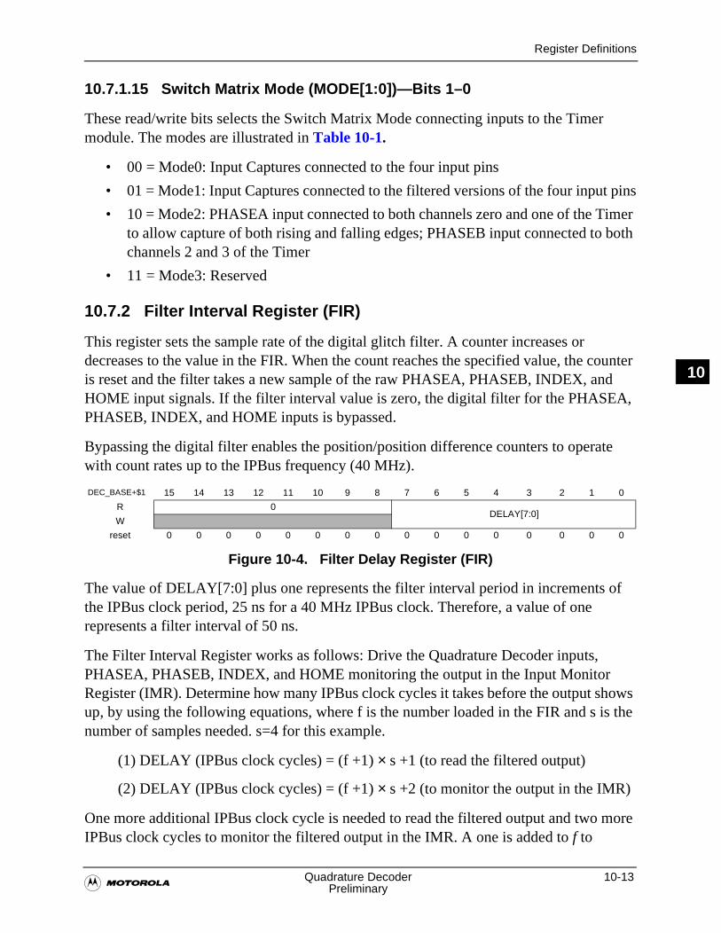
Register Definitions
�Quadrature Decoder 10-13
Preliminary
10
10.7.1.15 Switch Matrix Mode (MODE[1:0])—Bits 1–0
These read/write bits selects the Switch Matrix Mode connecting inputs to the Timer module. The modes are illustrated in Table 10-1.
• 00 = Mode0: Input Captures connected to the four input pins
• 01 = Mode1: Input Captures connected to the filtered versions of the four input pins
• 10 = Mode2: PHASEA input connected to both channels zero and one of the Timer to allow capture of both rising and falling edges; PHASEB input connected to both channels 2 and 3 of the Timer
• 11 = Mode3: Reserved
10.7.2 Filter Interval Register (FIR)
This register sets the sample rate of the digital glitch filter. A counter increases or decreases to the value in the FIR. When the count reaches the specified value, the counter is reset and the filter takes a new sample of the raw PHASEA, PHASEB, INDEX, and HOME input signals. If the filter interval value is zero, the digital filter for the PHASEA, PHASEB, INDEX, and HOME inputs is bypassed.
Bypassing the digital filter enables the position/position difference counters to operate with count rates up to the IPBus frequency (40 MHz).
The value of DELAY[7:0] plus one represents the filter interval period in increments of the IPBus clock period, 25 ns for a 40 MHz IPBus clock. Therefore, a value of one represents a filter interval of 50 ns.
The Filter Interval Register works as follows: Drive the Quadrature Decoder inputs, PHASEA, PHASEB, INDEX, and HOME monitoring the output in the Input Monitor Register (IMR). Determine how many IPBus clock cycles it takes before the output shows up, by using the following equations, where f is the number loaded in the FIR and s is the number of samples needed. s=4 for this example.
(1) DELAY (IPBus clock cycles) = (f +1) × s +1 (to read the filtered output)
(2) DELAY (IPBus clock cycles) = (f +1) × s +2 (to monitor the output in the IMR)
One more additional IPBus clock cycle is needed to read the filtered output and two more IPBus clock cycles to monitor the filtered output in the IMR. A one is added to f to
DEC_BASE+$1 15 14 13 12 11 10 9 8 7 6 5 4 3 2 1 0
R 0DELAY[7:0]
W
reset 0 0 0 0 0 0 0 0 0 0 0 0 0 0 0 0
Figure 10-4. Filter Delay Register (FIR)
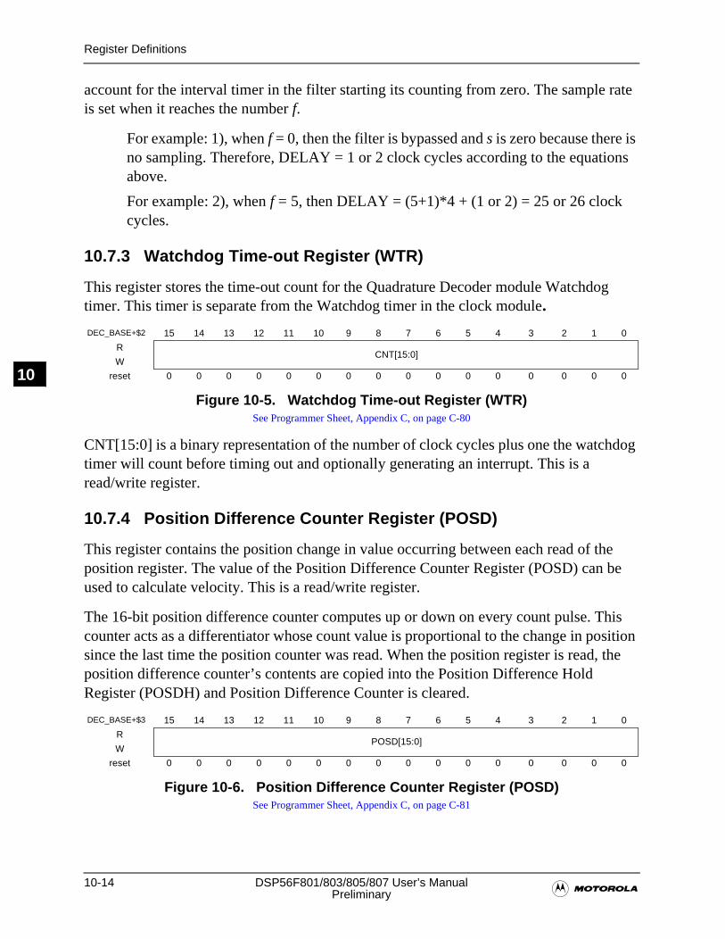
10-14 DSP56F801/803/805/807 User’s Manual�Preliminary
Register Definitions
10
account for the interval timer in the filter starting its counting from zero. The sample rate is set when it reaches the number f.
For example: 1), when f = 0, then the filter is bypassed and s is zero because there is no sampling. Therefore, DELAY = 1 or 2 clock cycles according to the equations above.
For example: 2), when f = 5, then DELAY = (5+1)*4 + (1 or 2) = 25 or 26 clock cycles.
10.7.3 Watchdog Time-out Register (WTR)
This register stores the time-out count for the Quadrature Decoder module Watchdog timer. This timer is separate from the Watchdog timer in the clock module.
CNT[15:0] is a binary representation of the number of clock cycles plus one the watchdog timer will count before timing out and optionally generating an interrupt. This is a read/write register.
10.7.4 Position Difference Counter Register (POSD)
This register contains the position change in value occurring between each read of the position register. The value of the Position Difference Counter Register (POSD) can be used to calculate velocity. This is a read/write register.
The 16-bit position difference counter computes up or down on every count pulse. This counter acts as a differentiator whose count value is proportional to the change in position since the last time the position counter was read. When the position register is read, the position difference counter’s contents are copied into the Position Difference Hold Register (POSDH) and Position Difference Counter is cleared.
DEC_BASE+$2 15 14 13 12 11 10 9 8 7 6 5 4 3 2 1 0
RCNT[15:0]
W
reset 0 0 0 0 0 0 0 0 0 0 0 0 0 0 0 0
Figure 10-5. Watchdog Time-out Register (WTR)See Programmer Sheet, Appendix C, on page C-80
DEC_BASE+$3 15 14 13 12 11 10 9 8 7 6 5 4 3 2 1 0
RPOSD[15:0]
W
reset 0 0 0 0 0 0 0 0 0 0 0 0 0 0 0 0
Figure 10-6. Position Difference Counter Register (POSD)See Programmer Sheet, Appendix C, on page C-81
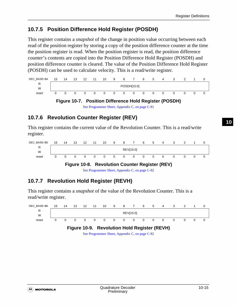
Register Definitions
�Quadrature Decoder 10-15
Preliminary
10
10.7.5 Position Difference Hold Register (POSDH)
This register contains a snapshot of the change in position value occurring between each read of the position register by storing a copy of the position difference counter at the time the position register is read. When the position register is read, the position difference counter’s contents are copied into the Position Difference Hold Register (POSDH) and position difference counter is cleared. The value of the Position Difference Hold Register (POSDH) can be used to calculate velocity. This is a read/write register.
10.7.6 Revolution Counter Register (REV)
This register contains the current value of the Revolution Counter. This is a read/write register.
10.7.7 Revolution Hold Register (REVH)
This register contains a snapshot of the value of the Revolution Counter. This is a read/write register.
DEC_BASE+$4 15 14 13 12 11 10 9 8 7 6 5 4 3 2 1 0
RPOSDH[15:0]
W
reset 0 0 0 0 0 0 0 0 0 0 0 0 0 0 0 0
Figure 10-7. Position Difference Hold Register (POSDH)See Programmer Sheet, Appendix C, on page C-81
DEC_BASE+$5 15 14 13 12 11 10 9 8 7 6 5 4 3 2 1 0
RREV[15:0]
W
reset 0 0 0 0 0 0 0 0 0 0 0 0 0 0 0 0
Figure 10-8. Revolution Counter Register (REV)See Programmer Sheet, Appendix C, on page C-82
DEC_BASE+$6 15 14 13 12 11 10 9 8 7 6 5 4 3 2 1 0
RREV[15:0]
W
reset 0 0 0 0 0 0 0 0 0 0 0 0 0 0 0 0
Figure 10-9. Revolution Hold Register (REVH)See Programmer Sheet, Appendix C, on page C-82
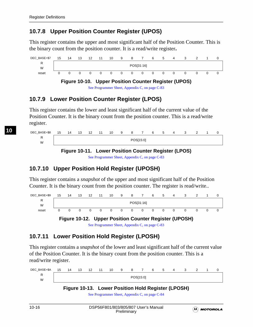
10-16 DSP56F801/803/805/807 User’s Manual�Preliminary
Register Definitions
10
10.7.8 Upper Position Counter Register (UPOS)
This register contains the upper and most significant half of the Position Counter. This is the binary count from the position counter. It is a read/write register.
10.7.9 Lower Position Counter Register (LPOS)
This register contains the lower and least significant half of the current value of the Position Counter. It is the binary count from the position counter. This is a read/write register.
10.7.10 Upper Position Hold Register (UPOSH)
This register contains a snapshot of the upper and most significant half of the Position Counter. It is the binary count from the position counter. The register is read/write..
10.7.11 Lower Position Hold Register (LPOSH)
This register contains a snapshot of the lower and least significant half of the current value of the Position Counter. It is the binary count from the position counter. This is a read/write register.
DEC_BASE+$7 15 14 13 12 11 10 9 8 7 6 5 4 3 2 1 0
RPOS[31:16]
W
reset 0 0 0 0 0 0 0 0 0 0 0 0 0 0 0 0
Figure 10-10. Upper Position Counter Register (UPOS)See Programmer Sheet, Appendix C, on page C-83
DEC_BASE+$8 15 14 13 12 11 10 9 8 7 6 5 4 3 2 1 0
RPOS[15:0]
W
Figure 10-11. Lower Position Counter Register (LPOS)See Programmer Sheet, Appendix C, on page C-83
DEC_BASE+$9 15 14 13 12 11 10 9 8 7 6 5 4 3 2 1 0
RPOS[31:16]
W
reset 0 0 0 0 0 0 0 0 0 0 0 0 0 0 0 0
Figure 10-12. Upper Position Counter Register (UPOSH)See Programmer Sheet, Appendix C, on page C-83
DEC_BASE+$A 15 14 13 12 11 10 9 8 7 6 5 4 3 2 1 0
RPOS[15:0]
W
Figure 10-13. Lower Position Hold Register (LPOSH)See Programmer Sheet, Appendix C, on page C-84
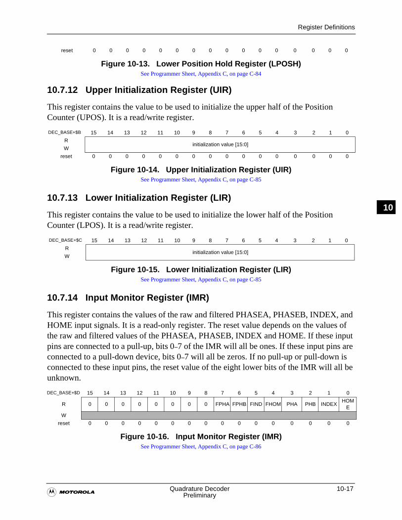
Register Definitions
�Quadrature Decoder 10-17
Preliminary
10
10.7.12 Upper Initialization Register (UIR)
This register contains the value to be used to initialize the upper half of the Position Counter (UPOS). It is a read/write register.
10.7.13 Lower Initialization Register (LIR)
This register contains the value to be used to initialize the lower half of the Position Counter (LPOS). It is a read/write register.
10.7.14 Input Monitor Register (IMR)
This register contains the values of the raw and filtered PHASEA, PHASEB, INDEX, and HOME input signals. It is a read-only register. The reset value depends on the values of the raw and filtered values of the PHASEA, PHASEB, INDEX and HOME. If these input pins are connected to a pull-up, bits 0–7 of the IMR will all be ones. If these input pins are connected to a pull-down device, bits 0–7 will all be zeros. If no pull-up or pull-down is connected to these input pins, the reset value of the eight lower bits of the IMR will all be unknown.
reset 0 0 0 0 0 0 0 0 0 0 0 0 0 0 0 0
DEC_BASE+$B 15 14 13 12 11 10 9 8 7 6 5 4 3 2 1 0
Rinitialization value [15:0]
W
reset 0 0 0 0 0 0 0 0 0 0 0 0 0 0 0 0
Figure 10-14. Upper Initialization Register (UIR)See Programmer Sheet, Appendix C, on page C-85
DEC_BASE+$C 15 14 13 12 11 10 9 8 7 6 5 4 3 2 1 0
Rinitialization value [15:0]
W
Figure 10-15. Lower Initialization Register (LIR)See Programmer Sheet, Appendix C, on page C-85
DEC_BASE+$D 15 14 13 12 11 10 9 8 7 6 5 4 3 2 1 0
R 0 0 0 0 0 0 0 0 FPHA FPHB FIND FHOM PHA PHB INDEXHOM
E
W
reset 0 0 0 0 0 0 0 0 0 0 0 0 0 0 0 0
Figure 10-16. Input Monitor Register (IMR)See Programmer Sheet, Appendix C, on page C-86
Figure 10-13. Lower Position Hold Register (LPOSH)See Programmer Sheet, Appendix C, on page C-84
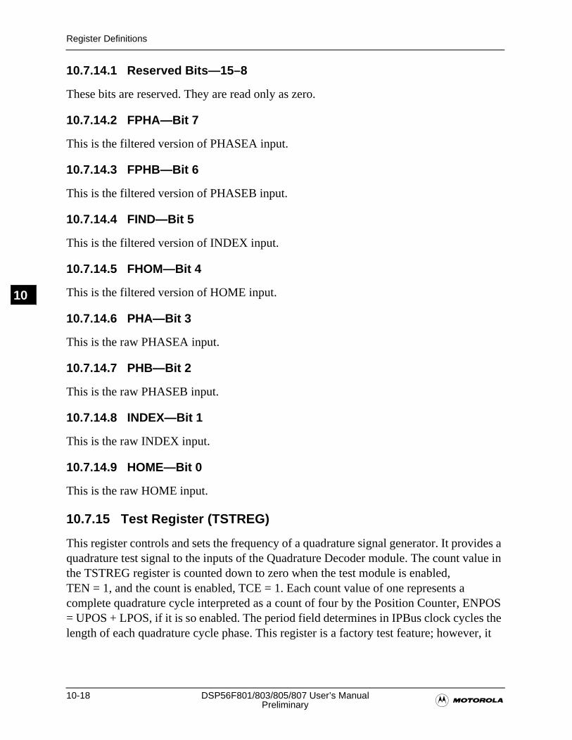
10-18 DSP56F801/803/805/807 User’s Manual�Preliminary
Register Definitions
10
10.7.14.1 Reserved Bits—15–8
These bits are reserved. They are read only as zero.
10.7.14.2 FPHA—Bit 7
This is the filtered version of PHASEA input.
10.7.14.3 FPHB—Bit 6
This is the filtered version of PHASEB input.
10.7.14.4 FIND—Bit 5
This is the filtered version of INDEX input.
10.7.14.5 FHOM—Bit 4
This is the filtered version of HOME input.
10.7.14.6 PHA—Bit 3
This is the raw PHASEA input.
10.7.14.7 PHB—Bit 2
This is the raw PHASEB input.
10.7.14.8 INDEX—Bit 1
This is the raw INDEX input.
10.7.14.9 HOME—Bit 0
This is the raw HOME input.
10.7.15 Test Register (TSTREG)
This register controls and sets the frequency of a quadrature signal generator. It provides a quadrature test signal to the inputs of the Quadrature Decoder module. The count value in the TSTREG register is counted down to zero when the test module is enabled, TEN = 1, and the count is enabled, TCE = 1. Each count value of one represents a complete quadrature cycle interpreted as a count of four by the Position Counter, ENPOS = UPOS + LPOS, if it is so enabled. The period field determines in IPBus clock cycles the length of each quadrature cycle phase. This register is a factory test feature; however, it
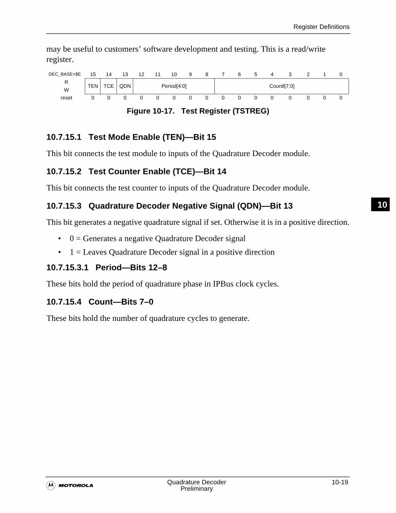
Register Definitions
�Quadrature Decoder 10-19
Preliminary
10
may be useful to customers’ software development and testing. This is a read/write register.
10.7.15.1 Test Mode Enable (TEN)—Bit 15
This bit connects the test module to inputs of the Quadrature Decoder module.
10.7.15.2 Test Counter Enable (TCE)—Bit 14
This bit connects the test counter to inputs of the Quadrature Decoder module.
10.7.15.3 Quadrature Decoder Negative Signal (QDN)—Bit 13
This bit generates a negative quadrature signal if set. Otherwise it is in a positive direction.
• 0 = Generates a negative Quadrature Decoder signal
• 1 = Leaves Quadrature Decoder signal in a positive direction
10.7.15.3.1 Period—Bits 12–8
These bits hold the period of quadrature phase in IPBus clock cycles.
10.7.15.4 Count—Bits 7–0
These bits hold the number of quadrature cycles to generate.
DEC_BASE+$E 15 14 13 12 11 10 9 8 7 6 5 4 3 2 1 0
RTEN TCE QDN Period[4:0] Countl[7:0]
W
reset 0 0 0 0 0 0 0 0 0 0 0 0 0 0 0 0
Figure 10-17. Test Register (TSTREG)

10-20 DSP56F801/803/805/807 User’s Manual�Preliminary
Register Definitions
10
�Pulse Width Modulator Module (PWM) 11-1
Preliminary
11
Chapter 11Pulse Width Modulator Module (PWM)

11-2 DSP56F801/803/805/807 User’s Manual�Preliminary
11
Features
�Pulse Width Modulator Module (PWM) 11-3
Preliminary
11
11.1 Introduction
The Pulse Width Modulator for Motor Control (PWM) can be configured for one, two, or three complementary pairs. For example:
• One complementary pair and four independent
• Two complementary pair and two independent
• Three complementary pair and zero independent
• Zero complementary pair and six independent
An application-specific feature of this part is the inclusion of PWM modules. These modules can each incorporate three complementary, individually programmable PWM signal outputs. To enhance motor control functionality each module is also capable of supporting six independent PWM functions for a total of 12-PWM outputs. Complementary operation permits programmable dead-time insertion, distortion correction through current sensing by software, and separate top and bottom output polarity control. The up-counter value is programmable to support a continuously variable PWM frequency. Both edge- and center-aligned synchronous pulse width-control, full zero percent to 100 percent modulation, are supported. The device is capable of controlling most motor types: AC Induction Motors (ACIM), both Brushless (BLDC) and Brush DC motors (BDC), Switched (SRM) and Variable Reluctance Motors (VRM), and stepper motors.
11.2 Features• Three complementary PWM signal pairs, or six independent PWM signals
• Features of complementary channel operation
— Deadtime insertion
— Separate top and bottom pulse width correction via current status inputs or software
— Separate top and bottom polarity control
• Edge-aligned or center-aligned PWM signals
• 15-bits of resolution
• Half-cycle reload capability
• Integral reload rates from one to 16
• Individual software-controlled PWM output
• Programmable fault protection
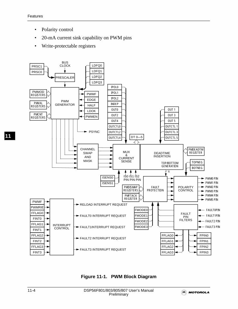
11-4 DSP56F801/803/805/807 User’s Manual�Preliminary
Features
11
• Polarity control
• 20-mA current sink capability on PWM pins
• Write-protectable registers
Figure 11-1. PWM Block Diagram
PWMRIE
PWMEN
LDOK
EDGE
OUTCTL0
OUT0
PRESCALER
PWM0 PINPWM1 PINPWM2 PINPWM3 PINPWM4 PINPWM5 PIN
PMDEADTMREGISTER
PWM
PRSC0
INTERRUPTCONTROL
FAULT
BUS
REGISTERSPMMOD
REGISTERSPMVAL
PMCNTREGISTERS
CLOCK
GENERATOR
MUX&
CURRENTSENSE
OUT2
OUT4
PROTECTION
FAULT3 PIN
FAULT0PIN
FAULT1PIN
FAULT2 PIN
REGISTERSPMDISMAP POLARITY
CONTROL
FAULTPIN
FILTERS
FFLAG0
PWMFRELOAD INTERRUPT REQUEST
FAULT0 INTERRUPT REQUEST
FAULT1INTERRUPT REQUEST
FAULT2 INTERRUPT REQUEST
FAULT3 INTERRUPT REQUEST
ISENS1
ISENS0
FINT0
FINT1
FINT2
FINT3
FFLAG0
FFLAG1
FFLAG2
FFLAG3
FMODE0
FMODE1
FMODE2
FMODE3
REGISTERPMFTACK
FPIN0
FPIN1
FPIN2
FPIN3
FFLAG2
FFLAG1
FFLAG3
LDFQ2
LDFQ3
PRSC1
OUTCTL2
OUTCTL4
OUTCTL 1
OUT 1
OUT 3
OUT 5
OUTCTL 3
OUTCTL 5
LDFQ1
LDFQ0
HALF
PWMF
INDEP
TOPNEG
BOTNEG
TOP/BOTTOMGENERATION
IPOL0
IPOL1
IPOL2
DT 0—5
PSYNC
6
IS0 IS1 IS2PIN PIN PIN
DEADTIME INSERTION
CHANNEL SWAP AND
MASK
Register Summary
�Pulse Width Modulator Module (PWM) 11-5
Preliminary
11
11.3 Pin Descriptions
The DSP56F801 and DSP56F803 have one Pulse Width Modulator with pins named PWMA0–5, ISA0–2, and FAULTA0–2. The DSP56F805 and DSP56F807 have two Pulse Width Modulators, PWMA and PWMB, with pins named PWMA0–5, ISA0–2, and FAULTA0–3 and PWMB0–5, ISA0–2 and FAULTB0–3.
11.3.1 PWM0–PWM5 Pins
PWM0–PWM5 are the output pins of the six PWM channels.
11.3.2 FAULT0–FAULT3 Pins
FAULT0–FAULT3 are input pins for disabling selected PWM outputs.
11.3.3 IS0–IS2 Pins
IS0–IS2 are current status pins for top/bottom pulse width correction in complementary channel operation while deadtime is asserted.
11.4 Register Summary
Each DSP56F801/803/805/807 Pulse Width Modulator has the following registers:
• PWM Control Register (PMCTL)
• PWM Fault Control Register (PMFCTL)
• PWM Fault Status Acknowledge (PMFSA)
• PWM Output Control Register (PMOUT)
• PWM Counter Register (PMCNT)
• PWM Counter Modulo Register (PWMCM)
• PWM Value Registers (PWMVAL0–5)
• PWM Deadtime Register (PMDEADTM)
• PWM Disable Mapping Register one (PMDISMAP1)
• PWM Disable Mapping Register two (PMDISMAP2)
• PWM Config Register (PMCFG)
• PWM Channel Control Register (PMCCR)
• PWM Port Register (PMPORT)
11-6 DSP56F801/803/805/807 User’s Manual�Preliminary
Functional Description
11
11.5 Functional Description
11.5.1 Block Diagram
A block diagram of the PWM is shown in Figure 11-1.
Note: The pad numbering starts with zero instead of one. Therefore, the PWM channels will be PWM[0:5], the faults FAULT[0:3], and the current sense pins IS[0:2].
11.5.2 Prescaler
To permit lower PWM frequencies, the prescaler produces the PWM clock frequency by dividing the IPBus clock frequency by one, two, four, and eight. The prescaler bits, PRSC0 and PRSC1, in the PWM control register (PWMCTL), select the prescaler divisor. This prescaler is buffered and will not be used by the PWM generator until the LDOK bit is set and a new PWM reload cycle begins.
Note: All peripherals, except the COP/Watchdog timer, run off of the IPBus clock frequency. It is the chip operating frequency divided by two. The maximum frequency of operation is 80 MHz and correlates to a 40 MHz IPBus Clock frequency. The PWM prescaler can scale this IPBus clock frequency by one, two, four, or eight.
11.5.3 PWM Generator
The PWM generator contains a 15-bit up/down PWM counter producing output signals with software-selectables:
• Alignment—The logic state of the EDGE bit in the configuration register determines whether the PWM output is edge-aligned or center-aligned.
• Period—The value written to the PWM counter modulos, PWMCM, register is used to determine the PWM period. The period can also be varied by using the prescaler
— With edge-aligned output, the modulus is the period of the PWM output in clock cycles.
— With center-aligned output, the modulus is one-half of the PWM output period in clock cycles.
• Pulse width—The number written to the PWM value register determines the pulse width duty cycle of the PWM output in clock cycles.
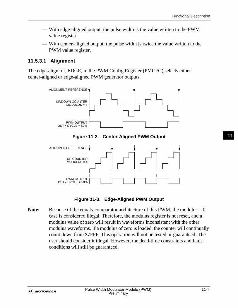
Functional Description
�Pulse Width Modulator Module (PWM) 11-7
Preliminary
11
— With edge-aligned output, the pulse width is the value written to the PWM value register.
— With center-aligned output, the pulse width is twice the value written to the PWM value register.
11.5.3.1 Alignment
The edge-align bit, EDGE, in the PWM Config Register (PMCFG) selects either center-aligned or edge-aligned PWM generator outputs.
Figure 11-2. Center-Aligned PWM Output
Figure 11-3. Edge-Aligned PWM Output
Note: Because of the equals-comparator architecture of this PWM, the modulus = 0 case is considered illegal. Therefore, the modulus register is not reset, and a modulus value of zero will result in waveforms inconsistent with the other modulus waveforms. If a modulus of zero is loaded, the counter will continually count down from $7FFF. This operation will not be tested or guaranteed. The user should consider it illegal. However, the dead-time constraints and fault conditions will still be guaranteed.
UP/DOWN COUNTERMODULUS = 4
ALIGNMENT REFERENCE
PWM OUTPUTDUTY CYCLE = 50%
UP COUNTERMODULUS = 4
ALIGNMENT REFERENCE
PWM OUTPUTDUTY CYCLE = 50%
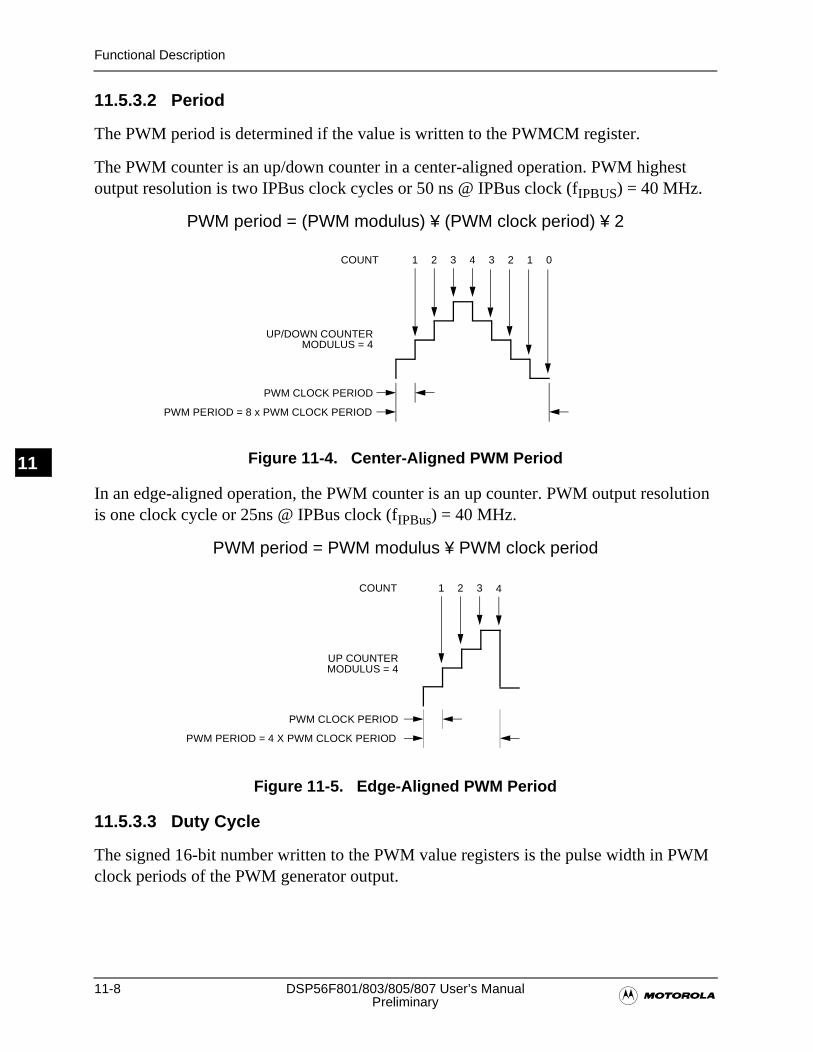
11-8 DSP56F801/803/805/807 User’s Manual�Preliminary
Functional Description
11
11.5.3.2 Period
The PWM period is determined if the value is written to the PWMCM register.
The PWM counter is an up/down counter in a center-aligned operation. PWM highest output resolution is two IPBus clock cycles or 50 ns @ IPBus clock (fIPBUS) = 40 MHz.
PWM period = (PWM modulus) ¥ (PWM clock period) ¥ 2
Figure 11-4. Center-Aligned PWM Period
In an edge-aligned operation, the PWM counter is an up counter. PWM output resolution is one clock cycle or 25ns @ IPBus clock (fIPBus) = 40 MHz.
PWM period = PWM modulus ¥ PWM clock period
Figure 11-5. Edge-Aligned PWM Period
11.5.3.3 Duty Cycle
The signed 16-bit number written to the PWM value registers is the pulse width in PWM clock periods of the PWM generator output.
UP/DOWN COUNTER
PWM CLOCK PERIOD
PWM PERIOD = 8 x PWM CLOCK PERIOD
MODULUS = 4
COUNT 1 2 3 4 3 2 1 0
UP COUNTER
PWM CLOCK PERIOD
PWM PERIOD = 4 X PWM CLOCK PERIOD
MODULUS = 4
COUNT 1 2 3 4
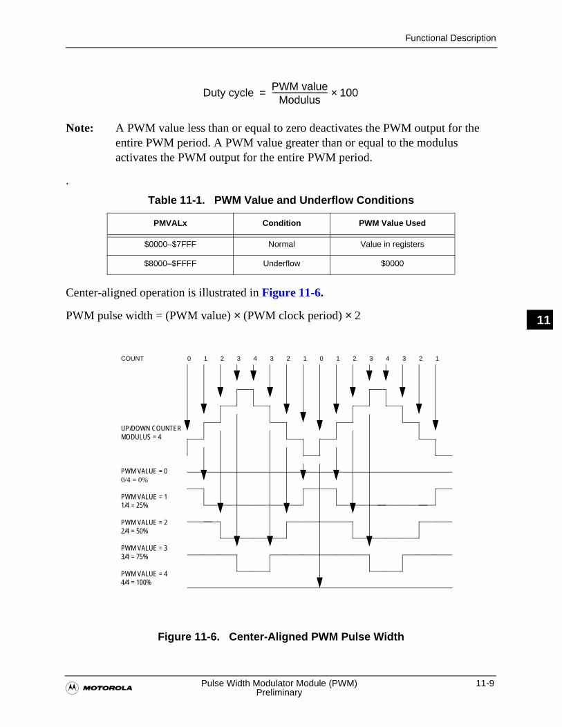
Functional Description
�Pulse Width Modulator Module (PWM) 11-9
Preliminary
11
Note: A PWM value less than or equal to zero deactivates the PWM output for the entire PWM period. A PWM value greater than or equal to the modulus activates the PWM output for the entire PWM period.
.
Center-aligned operation is illustrated in Figure 11-6.
PWM pulse width = (PWM value) × (PWM clock period) × 2
Figure 11-6. Center-Aligned PWM Pulse Width
Table 11-1. PWM Value and Underflow Conditions
PMVALx Condition PWM Value Used
$0000–$7FFF Normal Value in registers
$8000–$FFFF Underflow $0000
Duty cycle PWM valueModulus
------------------------------ 100×=
UP/DOWN COUNTERMODULUS = 4
PWM VALUE = 00/4 = 0%
PWM VALUE = 11/4 = 25%
PWM VALUE = 22/4 = 50%
PWM VALUE = 33/4 = 75%
PWM VALUE = 44/4 = 100%
COUNT 0 1 2 3 4 3 2 1 0 1 2 3 4 3 2 1
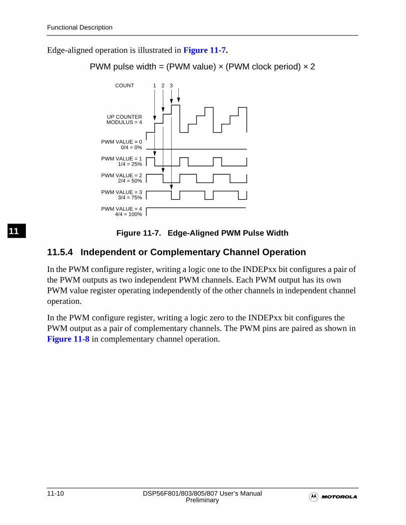
11-10 DSP56F801/803/805/807 User’s Manual�Preliminary
Functional Description
11
Edge-aligned operation is illustrated in Figure 11-7.
PWM pulse width = (PWM value) × (PWM clock period) × 2
Figure 11-7. Edge-Aligned PWM Pulse Width
11.5.4 Independent or Complementary Channel Operation
In the PWM configure register, writing a logic one to the INDEPxx bit configures a pair of the PWM outputs as two independent PWM channels. Each PWM output has its own PWM value register operating independently of the other channels in independent channel operation.
In the PWM configure register, writing a logic zero to the INDEPxx bit configures the PWM output as a pair of complementary channels. The PWM pins are paired as shown in Figure 11-8 in complementary channel operation.
UP COUNTER
PWM VALUE = 0
MODULUS = 4
PWM VALUE = 1
PWM VALUE = 2
PWM VALUE = 3
PWM VALUE = 4
0/4 = 0%
1/4 = 25%
2/4 = 50%
3/4 = 75%
4/4 = 100%
COUNT 1 2 3
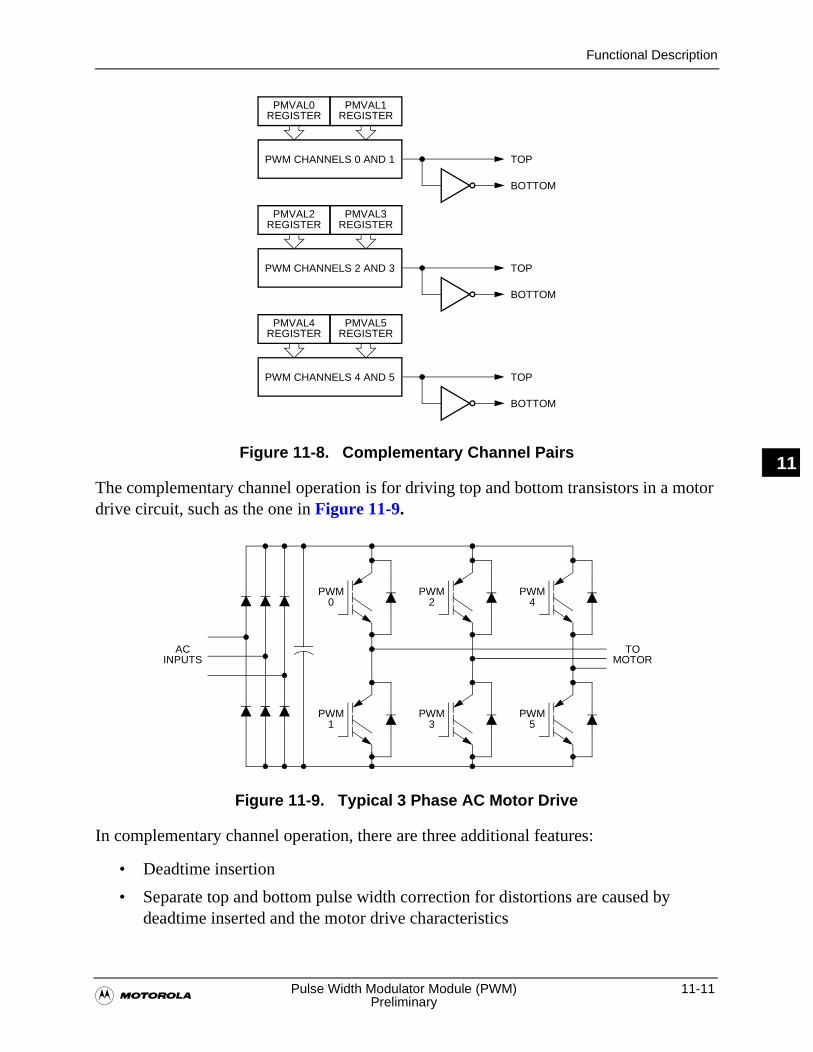
Functional Description
�Pulse Width Modulator Module (PWM) 11-11
Preliminary
11Figure 11-8. Complementary Channel Pairs
The complementary channel operation is for driving top and bottom transistors in a motor drive circuit, such as the one in Figure 11-9.
Figure 11-9. Typical 3 Phase AC Motor Drive
In complementary channel operation, there are three additional features:
• Deadtime insertion
• Separate top and bottom pulse width correction for distortions are caused by deadtime inserted and the motor drive characteristics
PWM CHANNELS 0 AND 1
PMVAL1
PWM CHANNELS 2 AND 3
PWM CHANNELS 4 AND 5
REGISTER
TOP
BOTTOM
TOP
BOTTOM
TOP
BOTTOM
PMVAL0REGISTER
PMVAL3REGISTER
PMVAL2REGISTER
PMVAL5REGISTER
PMVAL4REGISTER
PWM0
PWM2
ACINPUTS
TOMOTOR
PWM4
PWM3
PWM5
PWM1
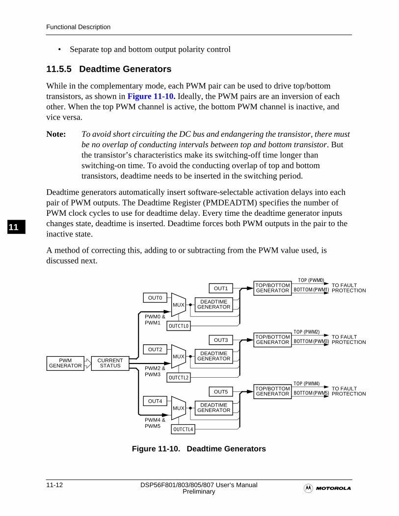
11-12 DSP56F801/803/805/807 User’s Manual�Preliminary
Functional Description
11
• Separate top and bottom output polarity control
11.5.5 Deadtime Generators
While in the complementary mode, each PWM pair can be used to drive top/bottom transistors, as shown in Figure 11-10. Ideally, the PWM pairs are an inversion of each other. When the top PWM channel is active, the bottom PWM channel is inactive, and vice versa.
Note: To avoid short circuiting the DC bus and endangering the transistor, there must be no overlap of conducting intervals between top and bottom transistor. But the transistor’s characteristics make its switching-off time longer than switching-on time. To avoid the conducting overlap of top and bottom transistors, deadtime needs to be inserted in the switching period.
Deadtime generators automatically insert software-selectable activation delays into each pair of PWM outputs. The Deadtime Register (PMDEADTM) specifies the number of PWM clock cycles to use for deadtime delay. Every time the deadtime generator inputs changes state, deadtime is inserted. Deadtime forces both PWM outputs in the pair to the inactive state.
A method of correcting this, adding to or subtracting from the PWM value used, is discussed next.
Figure 11-10. Deadtime Generators
MUXOUT0
OUTCTL0
MUXOUT2
OUTCTL2
MUXOUT4
OUTCTL4
PWMGENERATOR
CURRENTSTATUS
DEADTIMEGENERATOR
OUT1
DEADTIMEGENERATOR
DEADTIMEGENERATOR
PWM0 &
PWM2 &
PWM4 &
OUT3
OUT5
TOP/BOTTOMGENERATOR
TOP/BOTTOMGENERATOR
TOP/BOTTOMGENERATOR
TOP (PWM0)TO FAULTPROTECTION
TO FAULTPROTECTION
TO FAULTPROTECTION
BOTTOM (PWM1)
TOP (PWM2)
BOTTOM (PWM3)
TOP (PWM4)
BOTTOM (PWM5)
PWM1
PWM3
PWM5
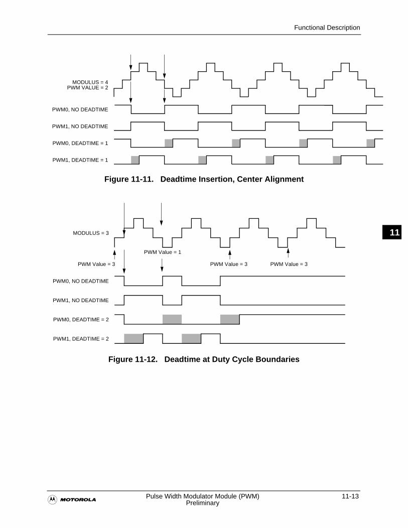
Functional Description
�Pulse Width Modulator Module (PWM) 11-13
Preliminary
11
Figure 11-11. Deadtime Insertion, Center Alignment
Figure 11-12. Deadtime at Duty Cycle Boundaries
PWM0, NO DEADTIME
PWM1, NO DEADTIME
PWM0, DEADTIME = 1
PWM1, DEADTIME = 1
MODULUS = 4PWM VALUE = 2
PWM0, NO DEADTIME
PWM1, NO DEADTIME
PWM0, DEADTIME = 2
PWM1, DEADTIME = 2
MODULUS = 3
PWM Value = 3 PWM Value = 3 PWM Value = 3
PWM Value = 1
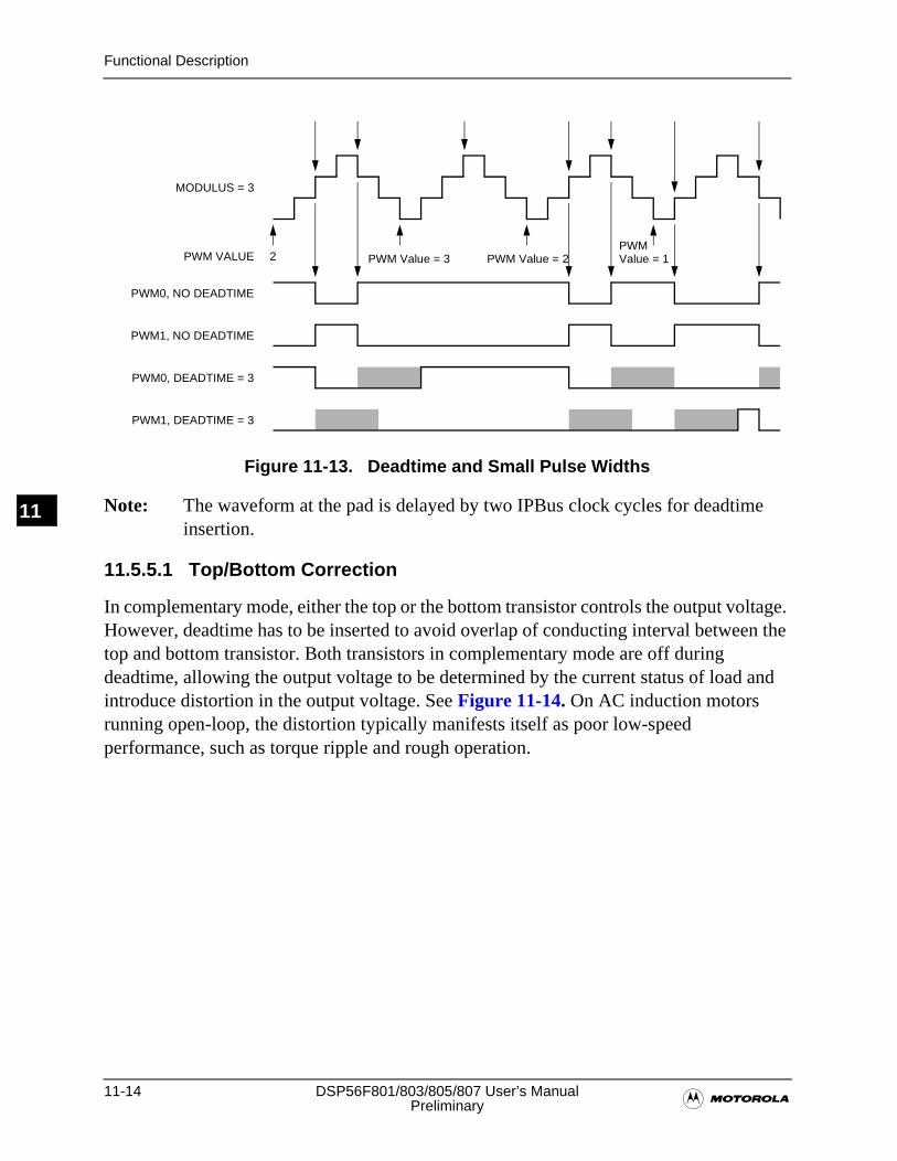
11-14 DSP56F801/803/805/807 User’s Manual�Preliminary
Functional Description
11
Figure 11-13. Deadtime and Small Pulse Widths
Note: The waveform at the pad is delayed by two IPBus clock cycles for deadtime insertion.
11.5.5.1 Top/Bottom Correction
In complementary mode, either the top or the bottom transistor controls the output voltage. However, deadtime has to be inserted to avoid overlap of conducting interval between the top and bottom transistor. Both transistors in complementary mode are off during deadtime, allowing the output voltage to be determined by the current status of load and introduce distortion in the output voltage. See Figure 11-14. On AC induction motors running open-loop, the distortion typically manifests itself as poor low-speed performance, such as torque ripple and rough operation.
MODULUS = 3
PWM0, NO DEADTIME
PWM0, DEADTIME = 3
PWM1, NO DEADTIME
PWM1, DEADTIME = 3
2PWM VALUEPWMValue = 1PWM Value = 2PWM Value = 3
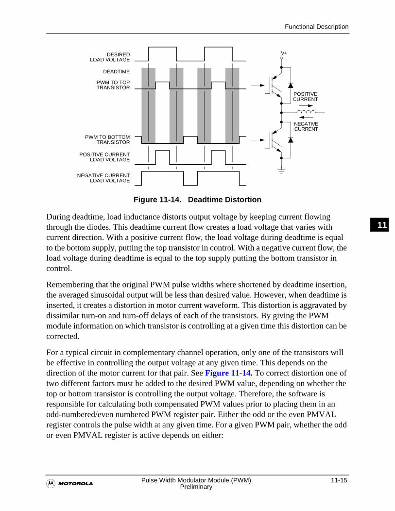
Functional Description
�Pulse Width Modulator Module (PWM) 11-15
Preliminary
11
Figure 11-14. Deadtime Distortion
During deadtime, load inductance distorts output voltage by keeping current flowing through the diodes. This deadtime current flow creates a load voltage that varies with current direction. With a positive current flow, the load voltage during deadtime is equal to the bottom supply, putting the top transistor in control. With a negative current flow, the load voltage during deadtime is equal to the top supply putting the bottom transistor in control.
Remembering that the original PWM pulse widths where shortened by deadtime insertion, the averaged sinusoidal output will be less than desired value. However, when deadtime is inserted, it creates a distortion in motor current waveform. This distortion is aggravated by dissimilar turn-on and turn-off delays of each of the transistors. By giving the PWM module information on which transistor is controlling at a given time this distortion can be corrected.
For a typical circuit in complementary channel operation, only one of the transistors will be effective in controlling the output voltage at any given time. This depends on the direction of the motor current for that pair. See Figure 11-14. To correct distortion one of two different factors must be added to the desired PWM value, depending on whether the top or bottom transistor is controlling the output voltage. Therefore, the software is responsible for calculating both compensated PWM values prior to placing them in an odd-numbered/even numbered PWM register pair. Either the odd or the even PMVAL register controls the pulse width at any given time. For a given PWM pair, whether the odd or even PMVAL register is active depends on either:
DESIRED
DEADTIME
PWM TO TOP
POSITIVE
NEGATIVE
PWM TO BOTTOM
POSITIVE CURRENT
NEGATIVE CURRENT
LOAD VOLTAGE
TRANSISTOR
TRANSISTOR
LOAD VOLTAGE
LOAD VOLTAGE
CURRENT
CURRENT
V+
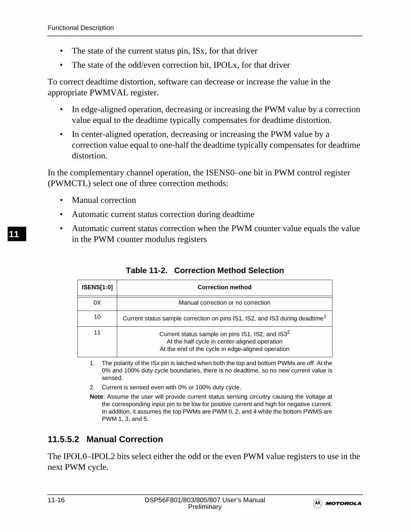
11-16 DSP56F801/803/805/807 User’s Manual�Preliminary
Functional Description
11
• The state of the current status pin, ISx, for that driver
• The state of the odd/even correction bit, IPOLx, for that driver
To correct deadtime distortion, software can decrease or increase the value in the appropriate PWMVAL register.
• In edge-aligned operation, decreasing or increasing the PWM value by a correction value equal to the deadtime typically compensates for deadtime distortion.
• In center-aligned operation, decreasing or increasing the PWM value by a correction value equal to one-half the deadtime typically compensates for deadtime distortion.
In the complementary channel operation, the ISENS0–one bit in PWM control register (PWMCTL) select one of three correction methods:
• Manual correction
• Automatic current status correction during deadtime
• Automatic current status correction when the PWM counter value equals the value in the PWM counter modulus registers
11.5.5.2 Manual Correction
The IPOL0–IPOL2 bits select either the odd or the even PWM value registers to use in the next PWM cycle.
Table 11-2. Correction Method Selection
ISENS[1:0] Correction method
0X Manual correction or no correction
10 Current status sample correction on pins IS1, IS2, and IS3 during deadtime1
1. The polarity of the ISx pin is latched when both the top and bottom PWMs are off. At the0% and 100% duty cycle boundaries, there is no deadtime, so no new current value issensed.
11 Current status sample on pins IS1, IS2, and IS32
At the half cycle in center-aligned operationAt the end of the cycle in edge-aligned operation
2. Current is sensed even with 0% or 100% duty cycle.
Note: Assume the user will provide current status sensing circuitry causing the voltage atthe corresponding input pin to be low for positive current and high for negative current.In addition, it assumes the top PWMs are PWM 0, 2, and 4 while the bottom PWMS arePWM 1, 3, and 5.
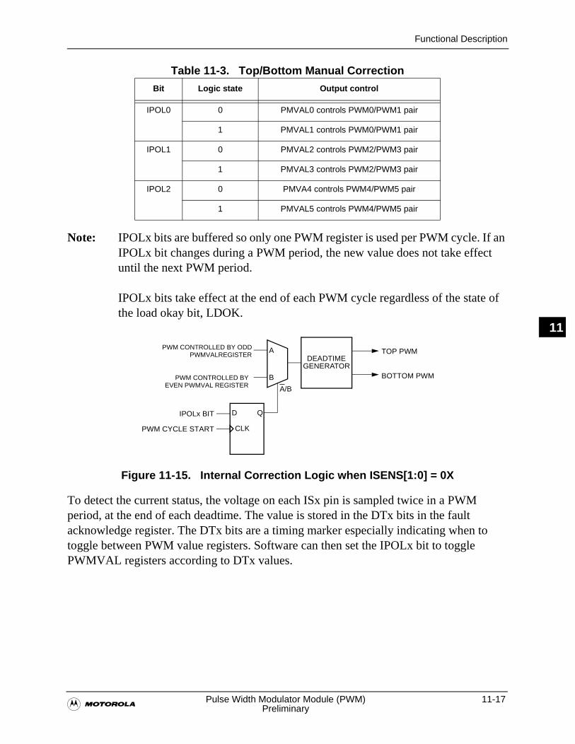
Functional Description
�Pulse Width Modulator Module (PWM) 11-17
Preliminary
11
Table 11-3. Top/Bottom Manual Correction
Note: IPOLx bits are buffered so only one PWM register is used per PWM cycle. If an IPOLx bit changes during a PWM period, the new value does not take effect until the next PWM period.
IPOLx bits take effect at the end of each PWM cycle regardless of the state of the load okay bit, LDOK.
Figure 11-15. Internal Correction Logic when ISENS[1:0] = 0X
To detect the current status, the voltage on each ISx pin is sampled twice in a PWM period, at the end of each deadtime. The value is stored in the DTx bits in the fault acknowledge register. The DTx bits are a timing marker especially indicating when to toggle between PWM value registers. Software can then set the IPOLx bit to toggle PWMVAL registers according to DTx values.
Bit Logic state Output control
IPOL0 0 PMVAL0 controls PWM0/PWM1 pair
1 PMVAL1 controls PWM0/PWM1 pair
IPOL1 0 PMVAL2 controls PWM2/PWM3 pair
1 PMVAL3 controls PWM2/PWM3 pair
IPOL2 0 PMVA4 controls PWM4/PWM5 pair
1 PMVAL5 controls PWM4/PWM5 pair
DEADTIMEGENERATOR
D Q
CLK
IPOLx BIT
A/B
A
B
TOP PWM
BOTTOM PWM
PWM CYCLE START
PWM CONTROLLED BY ODDPWMVALREGISTER
PWM CONTROLLED BYEVEN PWMVAL REGISTER
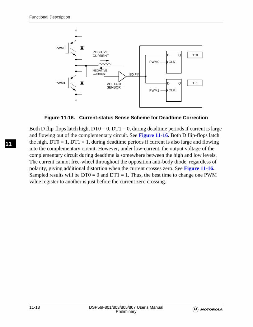
11-18 DSP56F801/803/805/807 User’s Manual�Preliminary
Functional Description
11
Figure 11-16. Current-status Sense Scheme for Deadtime Correction
Both D flip-flops latch high, DT0 = 0, DT1 = 0, during deadtime periods if current is large and flowing out of the complementary circuit. See Figure 11-16. Both D flip-flops latch the high, DT0 = 1, DT1 = 1, during deadtime periods if current is also large and flowing into the complementary circuit. However, under low-current, the output voltage of the complementary circuit during deadtime is somewhere between the high and low levels. The current cannot free-wheel throughout the opposition anti-body diode, regardless of polarity, giving additional distortion when the current crosses zero. See Figure 11-16. Sampled results will be DT0 = 0 and DT1 = 1. Thus, the best time to change one PWM value register to another is just before the current zero crossing.
PWM0
PWM1 D Q
CLK
D Q
CLK
VOLTAGESENSOR
IS0 PIN
PWM0
PWM1
DT0
DT1
POSITIVECURRENT
NEGATIVE CURRENT
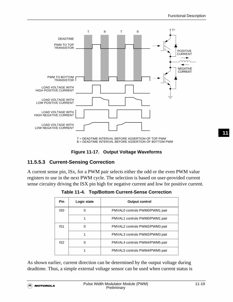
Functional Description
�Pulse Width Modulator Module (PWM) 11-19
Preliminary
11
Figure 11-17. Output Voltage Waveforms
11.5.5.3 Current-Sensing Correction
A current sense pin, ISx, for a PWM pair selects either the odd or the even PWM value registers to use in the next PWM cycle. The selection is based on user-provided current sense circuitry driving the ISX pin high for negative current and low for positive current.
As shown earlier, current direction can be determined by the output voltage during deadtime. Thus, a simple external voltage sensor can be used when current status is
Table 11-4. Top/Bottom Current-Sense Correction
Pin Logic state Output control
IS0 0 PMVAL0 controls PWM0/PWM1 pair
1 PMVAL1 controls PWM0/PWM1 pair
IS1 0 PMVAL2 controls PWM2/PWM3 pair
1 PMVAL3 controls PWM2/PWM3 pair
IS2 0 PMVAL4 controls PWM4/PWM5 pair
1 PMVAL5 controls PWM4/PWM5 pair
DEADTIME
PWM TO TOP
POSITIVE
NEGATIVE
PWM TO BOTTOM
LOAD VOLTAGE WITH
LOAD VOLTAGE WITH
TRANSISTOR
TRANSISTOR
HIGH POSITIVE CURRENT
LOW POSITIVE CURRENT
CURRENT
CURRENT
LOAD VOLTAGE WITHHIGH NEGATIVE CURRENT
LOAD VOLTAGE WITHLOW NEGATIVE CURRENT
T B T B
T = DEADTIME INTERVAL BEFORE ASSERTION OF TOP PWMB = DEADTIME INTERVAL BEFORE ASSERTION OF BOTTOM PWM
V+
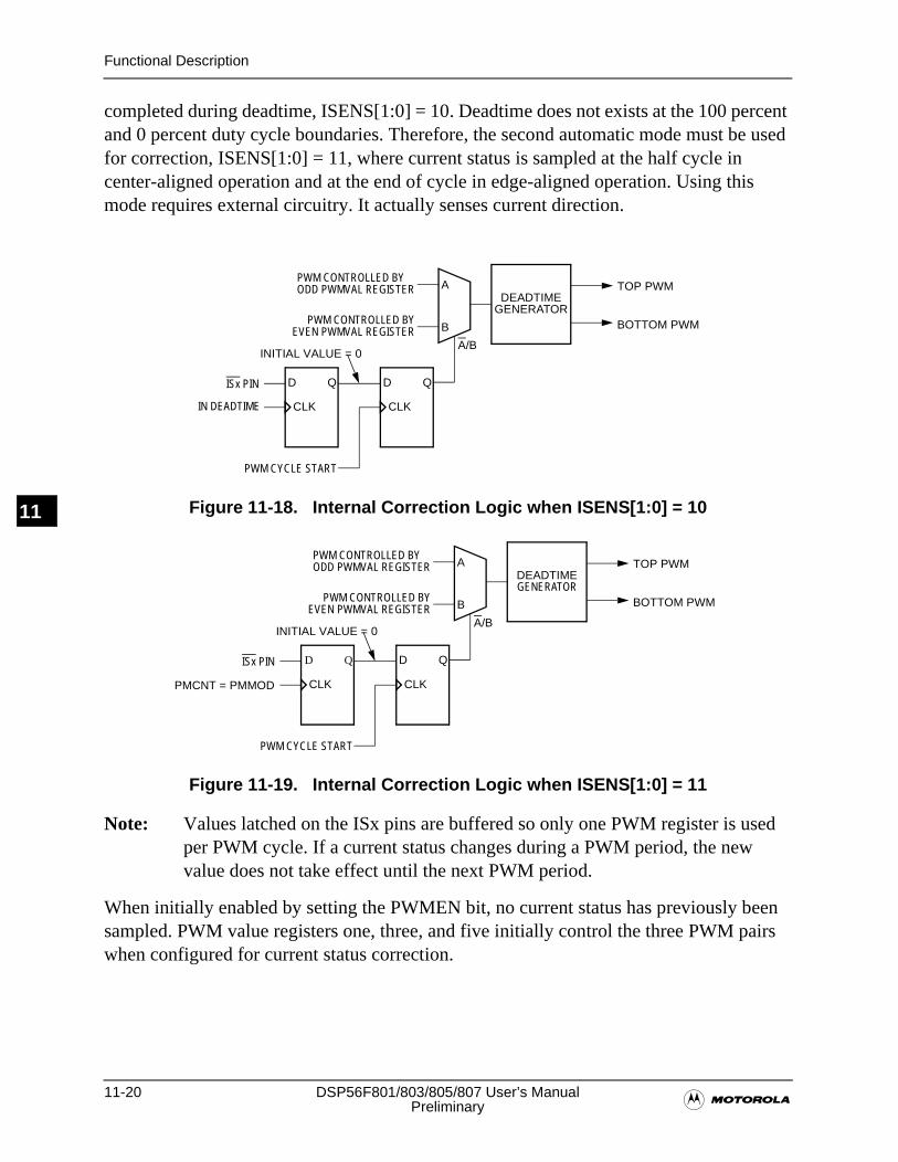
11-20 DSP56F801/803/805/807 User’s Manual�Preliminary
Functional Description
11
completed during deadtime, ISENS[1:0] = 10. Deadtime does not exists at the 100 percent and 0 percent duty cycle boundaries. Therefore, the second automatic mode must be used for correction, ISENS[1:0] = 11, where current status is sampled at the half cycle in center-aligned operation and at the end of cycle in edge-aligned operation. Using this mode requires external circuitry. It actually senses current direction.
Figure 11-18. Internal Correction Logic when ISENS[1:0] = 10
Figure 11-19. Internal Correction Logic when ISENS[1:0] = 11
Note: Values latched on the ISx pins are buffered so only one PWM register is used per PWM cycle. If a current status changes during a PWM period, the new value does not take effect until the next PWM period.
When initially enabled by setting the PWMEN bit, no current status has previously been sampled. PWM value registers one, three, and five initially control the three PWM pairs when configured for current status correction.
D Q
CLK
PWM CONTROLLED BY
PWM CONTROLLED BY
DEADTIMEGENERATOR
D Q
CLK
ISx PIN
A/B
A
B
PWM CYCLE START
TOP PWM
BOTTOM PWM
INITIAL VALUE = 0
ODD PWMVAL REGISTER
EVEN PWMVAL REGISTER
IN DEADTIME
D Q
CLK
PWM CONTROLLED BY
PWM CONTROLLED BY
DEADTIMEGENERATOR
D Q
CLK
ISx PIN
A/B
A
B
PWM CYCLE START
TOP PWM
BOTTOM PWM
INITIAL VALUE = 0
ODD PWMVAL REGISTER
EVEN PWMVAL REGISTER
PMCNT = PMMOD
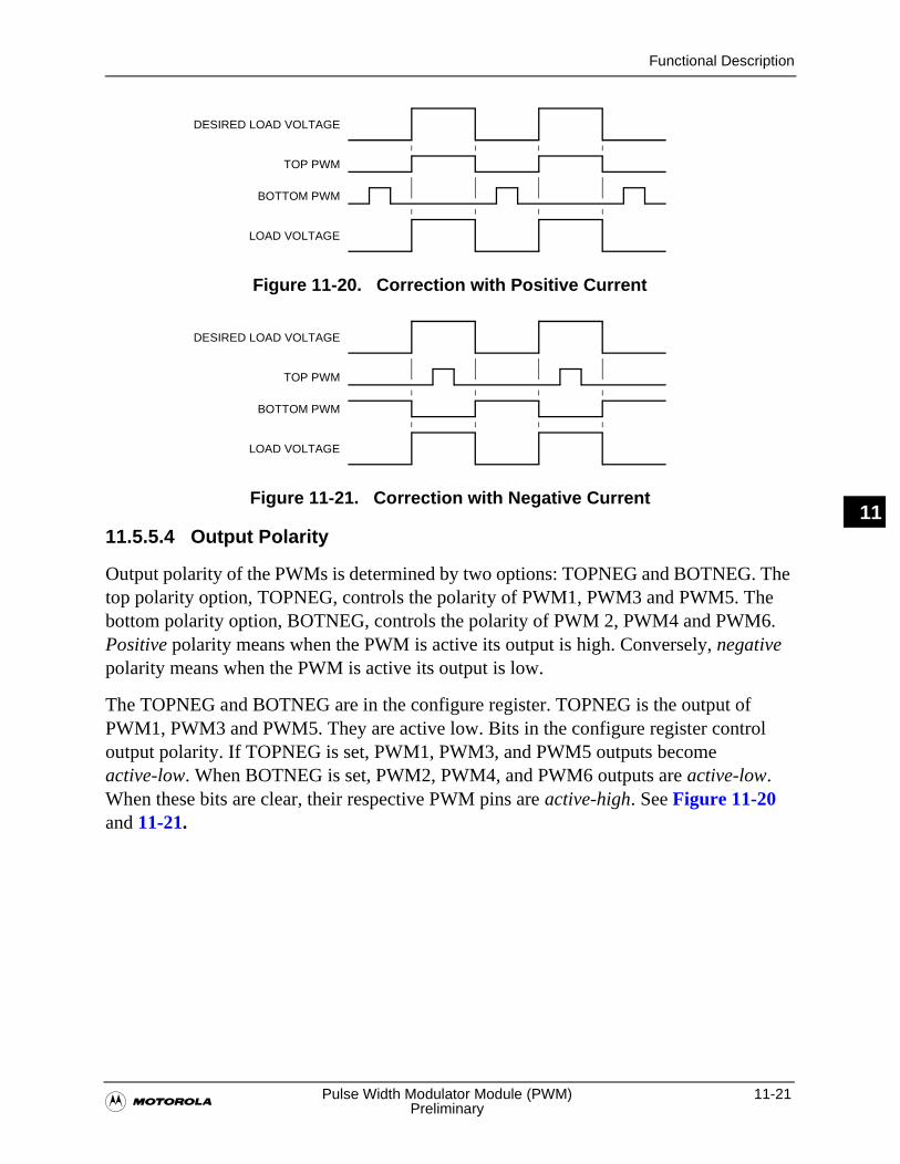
Functional Description
�Pulse Width Modulator Module (PWM) 11-21
Preliminary
11
Figure 11-20. Correction with Positive Current
Figure 11-21. Correction with Negative Current
11.5.5.4 Output Polarity
Output polarity of the PWMs is determined by two options: TOPNEG and BOTNEG. The top polarity option, TOPNEG, controls the polarity of PWM1, PWM3 and PWM5. The bottom polarity option, BOTNEG, controls the polarity of PWM 2, PWM4 and PWM6. Positive polarity means when the PWM is active its output is high. Conversely, negative polarity means when the PWM is active its output is low.
The TOPNEG and BOTNEG are in the configure register. TOPNEG is the output of PWM1, PWM3 and PWM5. They are active low. Bits in the configure register control output polarity. If TOPNEG is set, PWM1, PWM3, and PWM5 outputs become active-low. When BOTNEG is set, PWM2, PWM4, and PWM6 outputs are active-low. When these bits are clear, their respective PWM pins are active-high. See Figure 11-20 and 11-21.
DESIRED LOAD VOLTAGE
BOTTOM PWM
LOAD VOLTAGE
TOP PWM
DESIRED LOAD VOLTAGE
BOTTOM PWM
LOAD VOLTAGE
TOP PWM
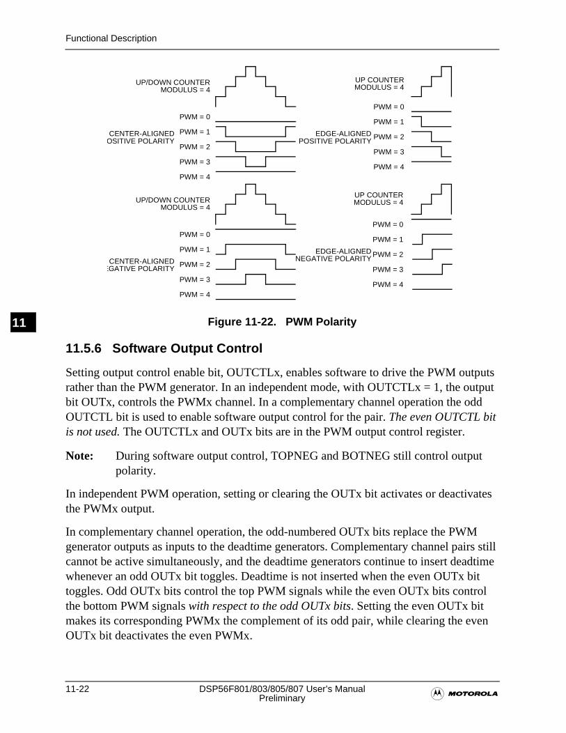
11-22 DSP56F801/803/805/807 User’s Manual�Preliminary
Functional Description
11 Figure 11-22. PWM Polarity
11.5.6 Software Output Control
Setting output control enable bit, OUTCTLx, enables software to drive the PWM outputs rather than the PWM generator. In an independent mode, with OUTCTLx = 1, the output bit OUTx, controls the PWMx channel. In a complementary channel operation the odd OUTCTL bit is used to enable software output control for the pair. The even OUTCTL bit is not used. The OUTCTLx and OUTx bits are in the PWM output control register.
Note: During software output control, TOPNEG and BOTNEG still control output polarity.
In independent PWM operation, setting or clearing the OUTx bit activates or deactivates the PWMx output.
In complementary channel operation, the odd-numbered OUTx bits replace the PWM generator outputs as inputs to the deadtime generators. Complementary channel pairs still cannot be active simultaneously, and the deadtime generators continue to insert deadtime whenever an odd OUTx bit toggles. Deadtime is not inserted when the even OUTx bit toggles. Odd OUTx bits control the top PWM signals while the even OUTx bits control the bottom PWM signals with respect to the odd OUTx bits. Setting the even OUTx bit makes its corresponding PWMx the complement of its odd pair, while clearing the even OUTx bit deactivates the even PWMx.
UP/DOWN COUNTER
PWM = 0
PWM = 1
PWM = 2
PWM = 3
PWM = 4
EDGE-ALIGNED
MODULUS = 4
UP/DOWN COUNTER
PWM = 0
PWM = 1
PWM = 2
PWM = 3
PWM = 4
MODULUS = 4
UP COUNTER
PWM = 0
PWM = 2
PWM = 3
PWM = 4
PWM = 1
MODULUS = 4
CENTER-ALIGNEDOSITIVE POLARITY POSITIVE POLARITY
UP COUNTER
PWM = 0
PWM = 2
PWM = 3
PWM = 4
PWM = 1
MODULUS = 4
CENTER-ALIGNEDEGATIVE POLARITY
EDGE-ALIGNEDNEGATIVE POLARITY
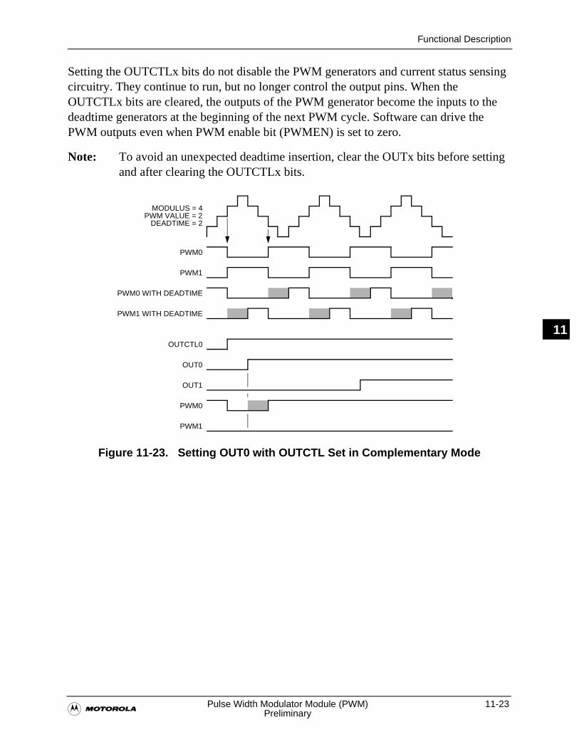
Functional Description
�Pulse Width Modulator Module (PWM) 11-23
Preliminary
11
Setting the OUTCTLx bits do not disable the PWM generators and current status sensing circuitry. They continue to run, but no longer control the output pins. When the OUTCTLx bits are cleared, the outputs of the PWM generator become the inputs to the deadtime generators at the beginning of the next PWM cycle. Software can drive the PWM outputs even when PWM enable bit (PWMEN) is set to zero.
Note: To avoid an unexpected deadtime insertion, clear the OUTx bits before setting and after clearing the OUTCTLx bits.
Figure 11-23. Setting OUT0 with OUTCTL Set in Complementary Mode
MODULUS = 4PWM VALUE = 2
DEADTIME = 2
PWM0
PWM1
PWM0 WITH DEADTIME
PWM1 WITH DEADTIME
OUTCTL0
OUT0
PWM0
PWM1
OUT1
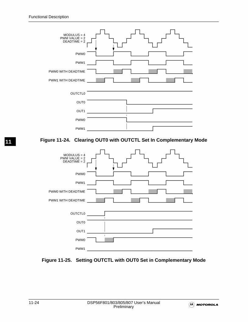
11-24 DSP56F801/803/805/807 User’s Manual�Preliminary
Functional Description
11 Figure 11-24. Clearing OUT0 with OUTCTL Set In Complementary Mode
Figure 11-25. Setting OUTCTL with OUT0 Set in Complementary Mode
MODULUS = 4PWM VALUE = 2
DEADTIME = 2
PWM0
PWM1
PWM0 WITH DEADTIME
PWM1 WITH DEADTIME
OUTCTL0
OUT0
PWM0
PWM1
OUT1
MODULUS = 4PWM VALUE = 2
DEADTIME = 2
PWM0
PWM1
PWM0 WITH DEADTIME
PWM1 WITH DEADTIME
OUTCTL0
OUT0
PWM0
PWM1
OUT1
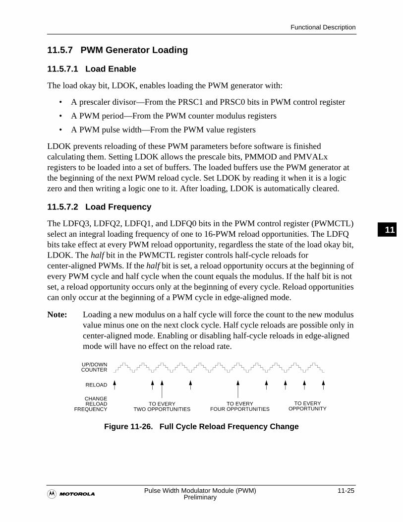
Functional Description
�Pulse Width Modulator Module (PWM) 11-25
Preliminary
11
11.5.7 PWM Generator Loading
11.5.7.1 Load Enable
The load okay bit, LDOK, enables loading the PWM generator with:
• A prescaler divisor—From the PRSC1 and PRSC0 bits in PWM control register
• A PWM period—From the PWM counter modulus registers
• A PWM pulse width—From the PWM value registers
LDOK prevents reloading of these PWM parameters before software is finished calculating them. Setting LDOK allows the prescale bits, PMMOD and PMVALx registers to be loaded into a set of buffers. The loaded buffers use the PWM generator at the beginning of the next PWM reload cycle. Set LDOK by reading it when it is a logic zero and then writing a logic one to it. After loading, LDOK is automatically cleared.
11.5.7.2 Load Frequency
The LDFQ3, LDFQ2, LDFQ1, and LDFQ0 bits in the PWM control register (PWMCTL) select an integral loading frequency of one to 16-PWM reload opportunities. The LDFQ bits take effect at every PWM reload opportunity, regardless the state of the load okay bit, LDOK. The half bit in the PWMCTL register controls half-cycle reloads for center-aligned PWMs. If the half bit is set, a reload opportunity occurs at the beginning of every PWM cycle and half cycle when the count equals the modulus. If the half bit is not set, a reload opportunity occurs only at the beginning of every cycle. Reload opportunities can only occur at the beginning of a PWM cycle in edge-aligned mode.
Note: Loading a new modulus on a half cycle will force the count to the new modulus value minus one on the next clock cycle. Half cycle reloads are possible only in center-aligned mode. Enabling or disabling half-cycle reloads in edge-aligned mode will have no effect on the reload rate.
Figure 11-26. Full Cycle Reload Frequency Change
RELOAD
CHANGE
UP/DOWN
TO EVERYTWO OPPORTUNITIES
TO EVERYOPPORTUNITY
COUNTER
RELOADFREQUENCY
TO EVERYFOUR OPPORTUNITIES
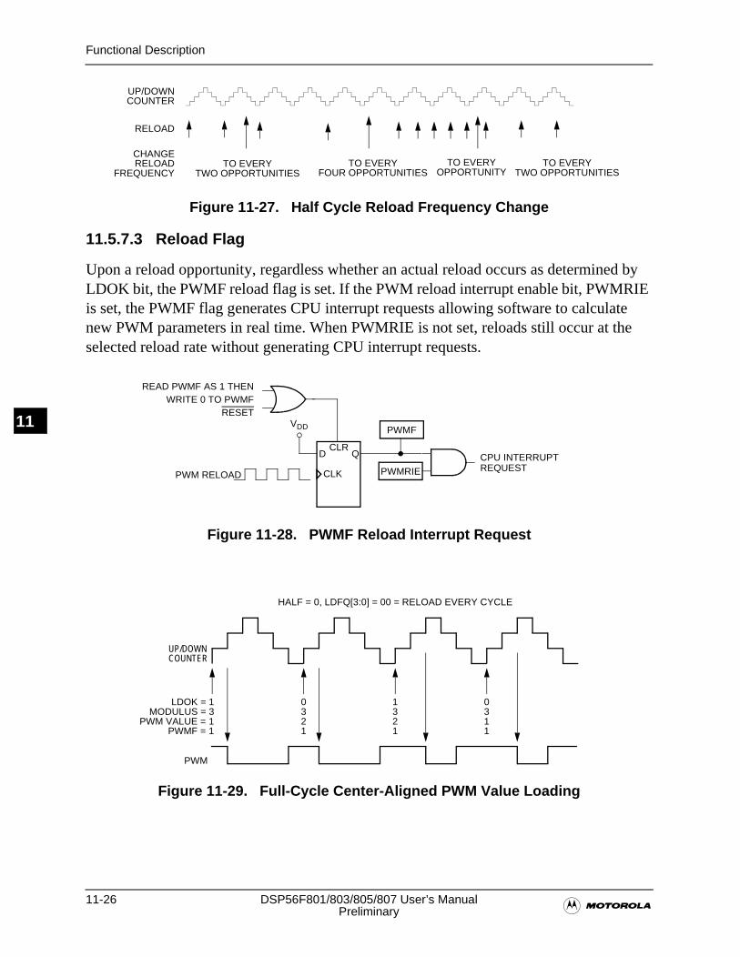
11-26 DSP56F801/803/805/807 User’s Manual�Preliminary
Functional Description
11
Figure 11-27. Half Cycle Reload Frequency Change
11.5.7.3 Reload Flag
Upon a reload opportunity, regardless whether an actual reload occurs as determined by LDOK bit, the PWMF reload flag is set. If the PWM reload interrupt enable bit, PWMRIE is set, the PWMF flag generates CPU interrupt requests allowing software to calculate new PWM parameters in real time. When PWMRIE is not set, reloads still occur at the selected reload rate without generating CPU interrupt requests.
Figure 11-28. PWMF Reload Interrupt Request
Figure 11-29. Full-Cycle Center-Aligned PWM Value Loading
RELOAD
CHANGE
UP/DOWN
TO EVERYTWO OPPORTUNITIES
TO EVERYOPPORTUNITY
COUNTER
RELOADFREQUENCY
TO EVERYTWO OPPORTUNITIES
TO EVERYFOUR OPPORTUNITIES
VDD
CPU INTERRUPT
PWM RELOADREQUEST
D Q
CLK
CLR
READ PWMF AS 1 THENWRITE 0 TO PWMF
RESET
PWMF
PWMRIE
PWM
HALF = 0, LDFQ[3:0] = 00 = RELOAD EVERY CYCLE
LDOK = 1MODULUS = 3
PWM VALUE = 1PWMF = 1
0321
1321
0311
UP/DOWNCOUNTER
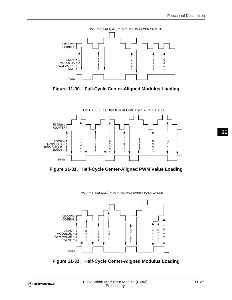
Functional Description
�Pulse Width Modulator Module (PWM) 11-27
Preliminary
11
Figure 11-30. Full-Cycle Center-Aligned Modulus Loading
Figure 11-31. Half-Cycle Center-Aligned PWM Value Loading
Figure 11-32. Half-Cycle Center-Aligned Modulus Loading
UP/DOWN
PWM
HALF = 0, LDFQ[3:0] = 00 = RELOAD EVERY CYCLE
LDOK = 1MODULUS = 2
PWM VALUE = 1PWMF = 1
1311
1211
1111
0211
COUNTER
PWM
HALF = 1, LDFQ[3:0] = 00 = RELOAD EVERY HALF-CYCLE
LDOK = 1MODULUS = 3
PWM VALUE = 1PWMF = 1
0321
1311
0331
UP/DOWNCOUNTER
1321
0321
1331
1311
UP/DOWN
PWM
HALF = 1, LDFQ[3:0] = 00 = RELOAD EVERY HALF-CYCLE
LDOK = 1MODULUS = 2
PWM VALUE = 1PWMF = 1
0311
0411
1111
0211
COUNTER
0211
1411
1411
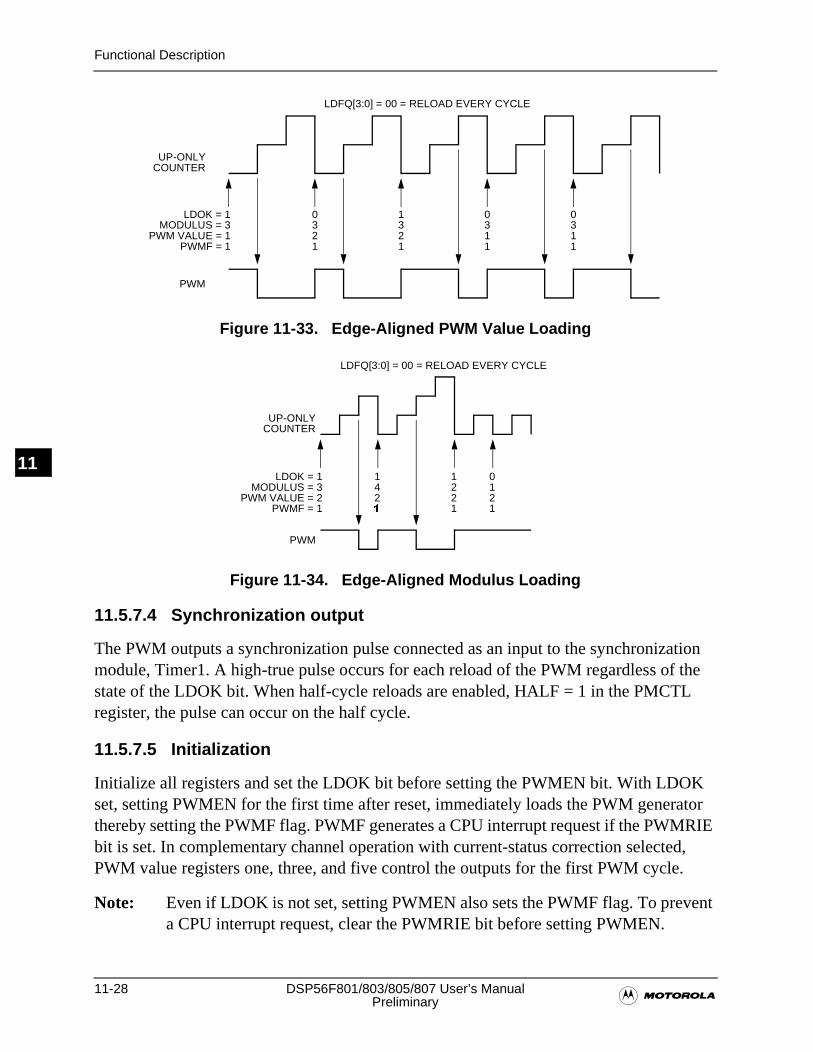
11-28 DSP56F801/803/805/807 User’s Manual�Preliminary
Functional Description
11
Figure 11-33. Edge-Aligned PWM Value Loading
Figure 11-34. Edge-Aligned Modulus Loading
11.5.7.4 Synchronization output
The PWM outputs a synchronization pulse connected as an input to the synchronization module, Timer1. A high-true pulse occurs for each reload of the PWM regardless of the state of the LDOK bit. When half-cycle reloads are enabled, HALF = 1 in the PMCTL register, the pulse can occur on the half cycle.
11.5.7.5 Initialization
Initialize all registers and set the LDOK bit before setting the PWMEN bit. With LDOK set, setting PWMEN for the first time after reset, immediately loads the PWM generator thereby setting the PWMF flag. PWMF generates a CPU interrupt request if the PWMRIE bit is set. In complementary channel operation with current-status correction selected, PWM value registers one, three, and five control the outputs for the first PWM cycle.
Note: Even if LDOK is not set, setting PWMEN also sets the PWMF flag. To prevent a CPU interrupt request, clear the PWMRIE bit before setting PWMEN.
UP-ONLY
PWM
LDFQ[3:0] = 00 = RELOAD EVERY CYCLE
COUNTER
LDOK = 1MODULUS = 3
PWM VALUE = 1PWMF = 1
0321
1321
0311
0311
UP-ONLY
PWM
LDFQ[3:0] = 00 = RELOAD EVERY CYCLE
LDOK = 1MODULUS = 3
PWM VALUE = 2PWMF = 1
COUNTER
142�
1221
0121
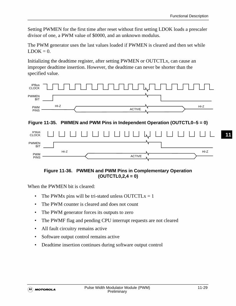
Functional Description
�Pulse Width Modulator Module (PWM) 11-29
Preliminary
11
Setting PWMEN for the first time after reset without first setting LDOK loads a prescaler divisor of one, a PWM value of $0000, and an unknown modulus.
The PWM generator uses the last values loaded if PWMEN is cleared and then set while LDOK = 0.
Initializing the deadtime register, after setting PWMEN or OUTCTLx, can cause an improper deadtime insertion. However, the deadtime can never be shorter than the specified value.
Figure 11-35. PWMEN and PWM Pins in Independent Operation (OUTCTL0–5 = 0)
Figure 11-36. PWMEN and PWM Pins in Complementary Operation (OUTCTL0,2,4 = 0)
When the PWMEN bit is cleared:
• The PWMx pins will be tri-stated unless OUTCTLx = 1
• The PWM counter is cleared and does not count
• The PWM generator forces its outputs to zero
• The PWMF flag and pending CPU interrupt requests are not cleared
• All fault circuitry remains active
• Software output control remains active
• Deadtime insertion continues during software output control
HI-ZACTIVE
HI-Z
IPBus
PWMEN
PWM
CLOCK
BIT
PINS
HI-Z
ACTIVE
IPBus
PWMEN
PWM
CLOCK
BIT
PINS
HI-Z
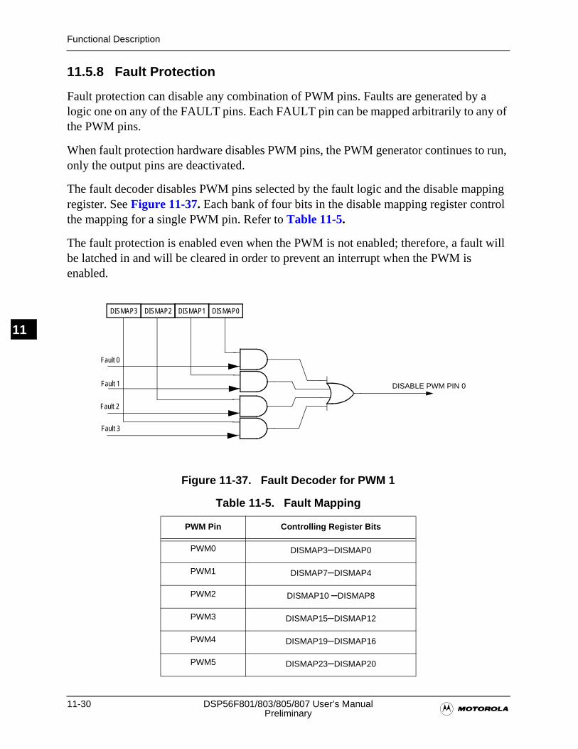
11-30 DSP56F801/803/805/807 User’s Manual�Preliminary
Functional Description
11
11.5.8 Fault Protection
Fault protection can disable any combination of PWM pins. Faults are generated by a logic one on any of the FAULT pins. Each FAULT pin can be mapped arbitrarily to any of the PWM pins.
When fault protection hardware disables PWM pins, the PWM generator continues to run, only the output pins are deactivated.
The fault decoder disables PWM pins selected by the fault logic and the disable mapping register. See Figure 11-37. Each bank of four bits in the disable mapping register control the mapping for a single PWM pin. Refer to Table 11-5.
The fault protection is enabled even when the PWM is not enabled; therefore, a fault will be latched in and will be cleared in order to prevent an interrupt when the PWM is enabled.
Figure 11-37. Fault Decoder for PWM 1
Table 11-5. Fault Mapping
PWM Pin Controlling Register Bits
PWM0 DISMAP3–DISMAP0
PWM1 DISMAP7–DISMAP4
PWM2 DISMAP10 –DISMAP8
PWM3 DISMAP15–DISMAP12
PWM4 DISMAP19–DISMAP16
PWM5 DISMAP23–DISMAP20
DISMAP0DISMAP1DISMAP2DISMAP3
DISABLE PWM PIN 0
Fault 0
Fault 1
Fault 2
Fault 3
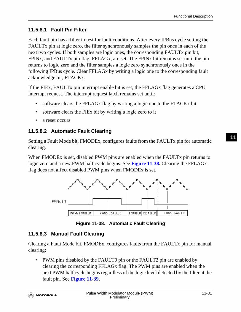
Functional Description
�Pulse Width Modulator Module (PWM) 11-31
Preliminary
11
11.5.8.1 Fault Pin Filter
Each fault pin has a filter to test for fault conditions. After every IPBus cycle setting the FAULTx pin at logic zero, the filter synchronously samples the pin once in each of the next two cycles. If both samples are logic ones, the corresponding FAULTx pin bit, FPINx, and FAULTx pin flag, FFLAGx, are set. The FPINx bit remains set until the pin returns to logic zero and the filter samples a logic zero synchronously once in the following IPBus cycle. Clear FFLAGx by writing a logic one to the corresponding fault acknowledge bit, FTACKx.
If the FIEx, FAULTx pin interrupt enable bit is set, the FFLAGx flag generates a CPU interrupt request. The interrupt request latch remains set until:
• software clears the FFLAGx flag by writing a logic one to the FTACKx bit
• software clears the FIEx bit by writing a logic zero to it
• a reset occurs
11.5.8.2 Automatic Fault Clearing
Setting a Fault Mode bit, FMODEx, configures faults from the FAULTx pin for automatic clearing.
When FMODEx is set, disabled PWM pins are enabled when the FAULTx pin returns to logic zero and a new PWM half cycle begins. See Figure 11-38. Clearing the FFLAGx flag does not affect disabled PWM pins when FMODEx is set.
Figure 11-38. Automatic Fault Clearing
11.5.8.3 Manual Fault Clearing
Clearing a Fault Mode bit, FMODEx, configures faults from the FAULTx pin for manual clearing:
• PWM pins disabled by the FAULT0 pin or the FAULT2 pin are enabled by clearing the corresponding FFLAGx flag. The PWM pins are enabled when the next PWM half cycle begins regardless of the logic level detected by the filter at the fault pin. See Figure 11-39.
PWMS ENABLED PWMS DISABLED PWMS ENABLED
FPINx BIT
DISABLEDENABLED
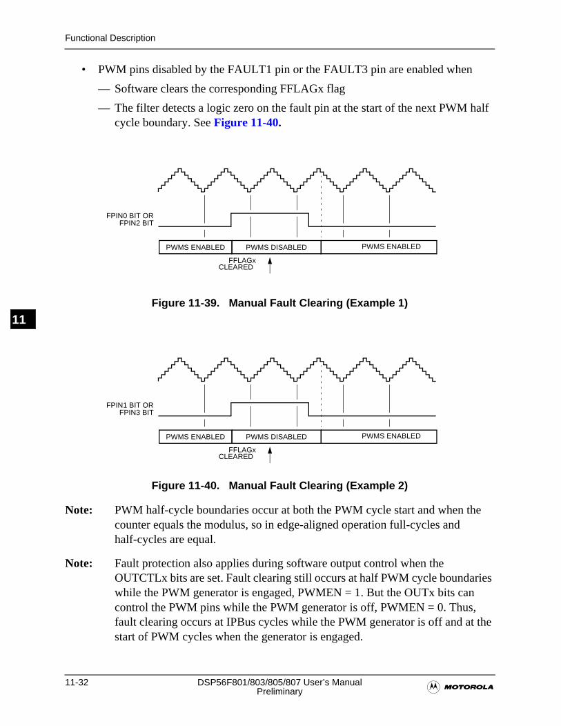
11-32 DSP56F801/803/805/807 User’s Manual�Preliminary
Functional Description
11
• PWM pins disabled by the FAULT1 pin or the FAULT3 pin are enabled when
— Software clears the corresponding FFLAGx flag
— The filter detects a logic zero on the fault pin at the start of the next PWM half cycle boundary. See Figure 11-40.
Figure 11-39. Manual Fault Clearing (Example 1)
Figure 11-40. Manual Fault Clearing (Example 2)
Note: PWM half-cycle boundaries occur at both the PWM cycle start and when the counter equals the modulus, so in edge-aligned operation full-cycles and half-cycles are equal.
Note: Fault protection also applies during software output control when the OUTCTLx bits are set. Fault clearing still occurs at half PWM cycle boundaries while the PWM generator is engaged, PWMEN = 1. But the OUTx bits can control the PWM pins while the PWM generator is off, PWMEN = 0. Thus, fault clearing occurs at IPBus cycles while the PWM generator is off and at the start of PWM cycles when the generator is engaged.
PWMS ENABLED
FPIN0 BIT ORFPIN2 BIT
PWMS ENABLED PWMS DISABLED
FFLAGxCLEARED
PWMS ENABLED
FPIN1 BIT ORFPIN3 BIT
PWMS ENABLED PWMS DISABLED
FFLAGxCLEARED
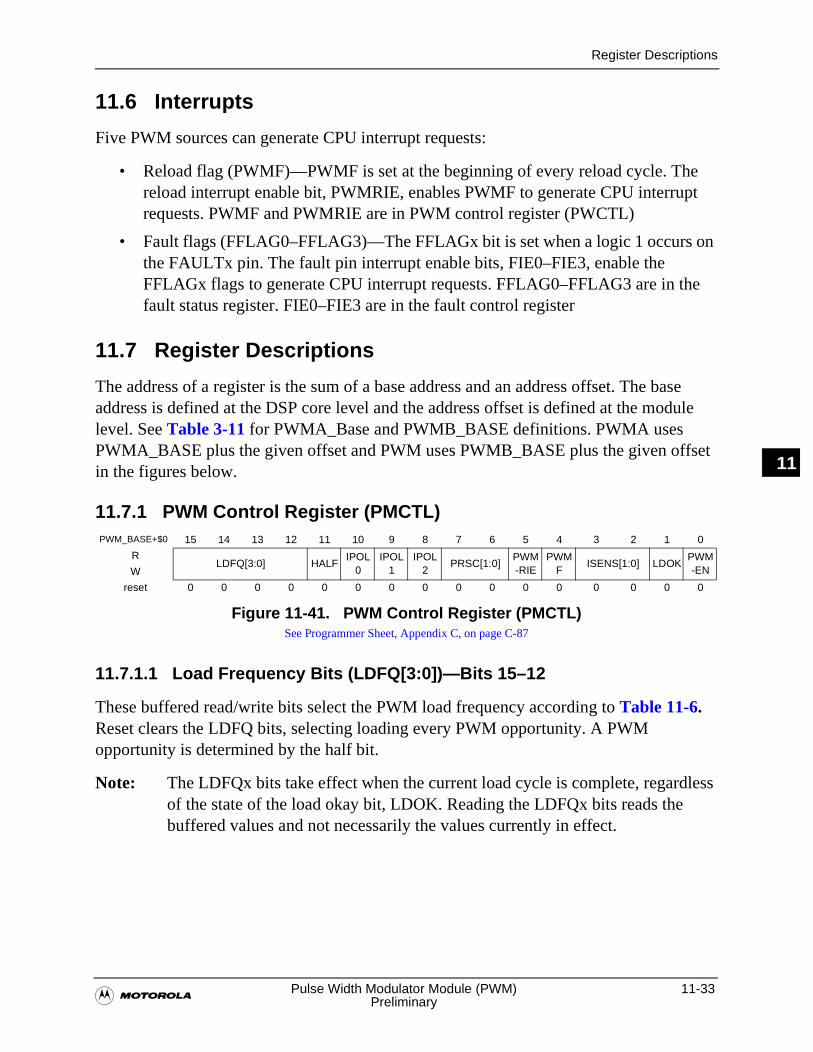
Register Descriptions
�Pulse Width Modulator Module (PWM) 11-33
Preliminary
11
11.6 Interrupts
Five PWM sources can generate CPU interrupt requests:
• Reload flag (PWMF)—PWMF is set at the beginning of every reload cycle. The reload interrupt enable bit, PWMRIE, enables PWMF to generate CPU interrupt requests. PWMF and PWMRIE are in PWM control register (PWCTL)
• Fault flags (FFLAG0–FFLAG3)—The FFLAGx bit is set when a logic 1 occurs on the FAULTx pin. The fault pin interrupt enable bits, FIE0–FIE3, enable the FFLAGx flags to generate CPU interrupt requests. FFLAG0–FFLAG3 are in the fault status register. FIE0–FIE3 are in the fault control register
11.7 Register Descriptions
The address of a register is the sum of a base address and an address offset. The base address is defined at the DSP core level and the address offset is defined at the module level. See Table 3-11 for PWMA_Base and PWMB_BASE definitions. PWMA uses PWMA_BASE plus the given offset and PWM uses PWMB_BASE plus the given offset in the figures below.
11.7.1 PWM Control Register (PMCTL)
Figure 11-41. PWM Control Register (PMCTL)See Programmer Sheet, Appendix C, on page C-87
11.7.1.1 Load Frequency Bits (LDFQ[3:0])—Bits 15–12
These buffered read/write bits select the PWM load frequency according to Table 11-6. Reset clears the LDFQ bits, selecting loading every PWM opportunity. A PWM opportunity is determined by the half bit.
Note: The LDFQx bits take effect when the current load cycle is complete, regardless of the state of the load okay bit, LDOK. Reading the LDFQx bits reads the buffered values and not necessarily the values currently in effect.
PWM_BASE+$0 15 14 13 12 11 10 9 8 7 6 5 4 3 2 1 0
RLDFQ[3:0] HALF
IPOL0
IPOL1
IPOL2
PRSC[1:0]PWM-RIE
PWMF
ISENS[1:0] LDOKPWM-ENW
reset 0 0 0 0 0 0 0 0 0 0 0 0 0 0 0 0
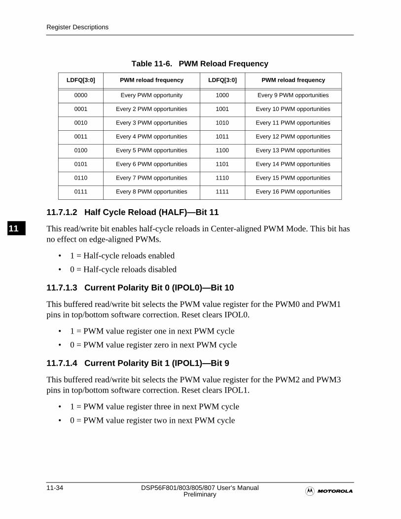
11-34 DSP56F801/803/805/807 User’s Manual�Preliminary
Register Descriptions
11
11.7.1.2 Half Cycle Reload (HALF)—Bit 11
This read/write bit enables half-cycle reloads in Center-aligned PWM Mode. This bit has no effect on edge-aligned PWMs.
• 1 = Half-cycle reloads enabled
• 0 = Half-cycle reloads disabled
11.7.1.3 Current Polarity Bit 0 (IPOL0)—Bit 10
This buffered read/write bit selects the PWM value register for the PWM0 and PWM1 pins in top/bottom software correction. Reset clears IPOL0.
• 1 = PWM value register one in next PWM cycle
• 0 = PWM value register zero in next PWM cycle
11.7.1.4 Current Polarity Bit 1 (IPOL1)—Bit 9
This buffered read/write bit selects the PWM value register for the PWM2 and PWM3 pins in top/bottom software correction. Reset clears IPOL1.
• 1 = PWM value register three in next PWM cycle
• 0 = PWM value register two in next PWM cycle
Table 11-6. PWM Reload Frequency
LDFQ[3:0] PWM reload frequency LDFQ[3:0] PWM reload frequency
0000 Every PWM opportunity 1000 Every 9 PWM opportunities
0001 Every 2 PWM opportunities 1001 Every 10 PWM opportunities
0010 Every 3 PWM opportunities 1010 Every 11 PWM opportunities
0011 Every 4 PWM opportunities 1011 Every 12 PWM opportunities
0100 Every 5 PWM opportunities 1100 Every 13 PWM opportunities
0101 Every 6 PWM opportunities 1101 Every 14 PWM opportunities
0110 Every 7 PWM opportunities 1110 Every 15 PWM opportunities
0111 Every 8 PWM opportunities 1111 Every 16 PWM opportunities
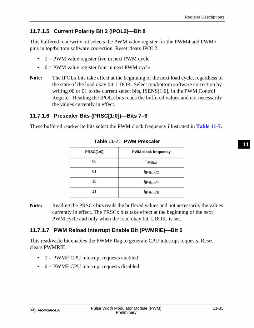
Register Descriptions
�Pulse Width Modulator Module (PWM) 11-35
Preliminary
11
11.7.1.5 Current Polarity Bit 2 (IPOL2)—Bit 8
This buffered read/write bit selects the PWM value register for the PWM4 and PWM5 pins in top/bottom software correction. Reset clears IPOL2.
• 1 = PWM value register five in next PWM cycle
• 0 = PWM value register four in next PWM cycle
Note: The IPOLx bits take effect at the beginning of the next load cycle, regardless of the state of the load okay bit, LDOK. Select top/bottom software correction by writing 00 or 01 to the current select bits, ISENS[1:0], in the PWM Control Register. Reading the IPOLx bits reads the buffered values and not necessarily the values currently in effect.
11.7.1.6 Prescaler Bits (PRSC[1:0])—Bits 7–6
These buffered read/write bits select the PWM clock frequency illustrated in Table 11-7.
Note: Reading the PRSCx bits reads the buffered values and not necessarily the values currently in effect. The PRSCx bits take effect at the beginning of the next PWM cycle and only when the load okay bit, LDOK, is set.
11.7.1.7 PWM Reload Interrupt Enable Bit (PWMRIE)—Bit 5
This read/write bit enables the PWMF flag to generate CPU interrupt requests. Reset clears PWMRIE.
• 1 = PWMF CPU interrupt requests enabled
• 0 = PWMF CPU interrupt requests disabled
Table 11-7. PWM Prescaler
PRSC[1:0] PWM clock frequency
00 fIPBus
01 fIPBus/2
10 fIPBus/4
11 fIPBus/8
11-36 DSP56F801/803/805/807 User’s Manual�Preliminary
Register Descriptions
11
11.7.1.8 PWM Reload Flag (PWMF)—Bit 4
This read/write flag is set at the beginning of every reload cycle regardless of the state of the LDOK bit. Clear PWMF by reading PWM control register with PWMF set and then writing a logic zero to the PWMF bit. If another reload occurs before the clearing sequence is complete, then writing logic zero to PWMF has no effect. Reset clears PWMF.
• 1 = New reload cycle since last PWMF clearing
• 0 = No new reload cycle since last PWMF clearing
Note: Clearing PWMF clears pending PWMF CPU interrupt requests.
11.7.1.9 Current Status Bits (ISENS[1:0])—Bits 3–2
These read/write bits select the top/bottom correction scheme, illustrated in Table 11-2. Reset clears the ISENSx bits, selecting software correction or no correction.
Note: The ISENSx bits are not buffered. Changing the current status sensing method can affect the present PWM cycle.
11.7.1.10 Load Okay Bit (LDOK)—Bit 1
This read/write bit loads the prescaler bits of PMCTL and the entire PMMOD and PWMVAL registers into a set of buffers. The buffered prescaler divisor, PWM counter modulus value, and PWM pulse width take effect at the next PWM reload. Set LDOK by reading it when it is logic zero and then writing a logic one to it. LDOK is automatically cleared after the new values are loaded, or can be manually cleared before a reload by writing a logic zero to it. Reset clears LDOK.
• 1 = Load prescaler, modulus, and PWM values
• 0 = Do not load new modulus, prescaler, and PWM values
11.7.1.11 PWM Enable Bit (PWMEN)—Bit 0
This read/write bit enables the PWM generator and the PWM pins. When PWMEN = 0, the PWM pins are in their inactive states unless OUTCTLx = 1. Reset clears PWMEN.
• 1 = PWM generator and PWM pins enabled
• 0 = PWM generator and PWM pins disabled unless OUTCTL = 1
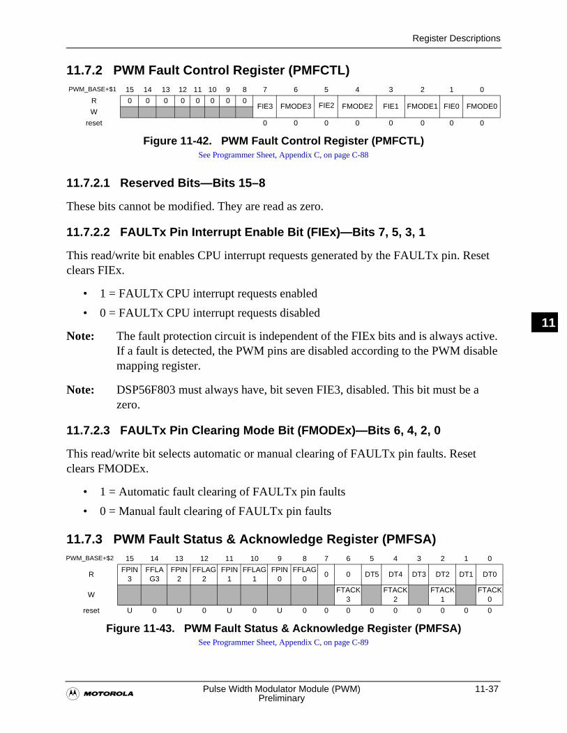
Register Descriptions
�Pulse Width Modulator Module (PWM) 11-37
Preliminary
11
11.7.2 PWM Fault Control Register (PMFCTL)
Figure 11-42. PWM Fault Control Register (PMFCTL)See Programmer Sheet, Appendix C, on page C-88
11.7.2.1 Reserved Bits—Bits 15–8
These bits cannot be modified. They are read as zero.
11.7.2.2 FAULTx Pin Interrupt Enable Bit (FIEx)—Bits 7, 5, 3, 1
This read/write bit enables CPU interrupt requests generated by the FAULTx pin. Reset clears FIEx.
• 1 = FAULTx CPU interrupt requests enabled
• 0 = FAULTx CPU interrupt requests disabled
Note: The fault protection circuit is independent of the FIEx bits and is always active. If a fault is detected, the PWM pins are disabled according to the PWM disable mapping register.
Note: DSP56F803 must always have, bit seven FIE3, disabled. This bit must be a zero.
11.7.2.3 FAULTx Pin Clearing Mode Bit (FMODEx)—Bits 6, 4, 2, 0
This read/write bit selects automatic or manual clearing of FAULTx pin faults. Reset clears FMODEx.
• 1 = Automatic fault clearing of FAULTx pin faults
• 0 = Manual fault clearing of FAULTx pin faults
11.7.3 PWM Fault Status & Acknowledge Register (PMFSA)
Figure 11-43. PWM Fault Status & Acknowledge Register (PMFSA)See Programmer Sheet, Appendix C, on page C-89
PWM_BASE+$1 15 14 13 12 11 10 9 8 7 6 5 4 3 2 1 0
R 0 0 0 0 0 0 0 0FIE3 FMODE3 FIE2 FMODE2 FIE1 FMODE1 FIE0 FMODE0
W
reset 0 0 0 0 0 0 0 0
PWM_BASE+$2 15 14 13 12 11 10 9 8 7 6 5 4 3 2 1 0
RFPIN
3FFLA
G3FPIN
2FFLAG
2FPIN
1FFLAG
1FPIN
0FFLAG
00 0 DT5 DT4 DT3 DT2 DT1 DT0
WFTACK
3FTACK
2FTACK
1FTACK
0
reset U 0 U 0 U 0 U 0 0 0 0 0 0 0 0 0
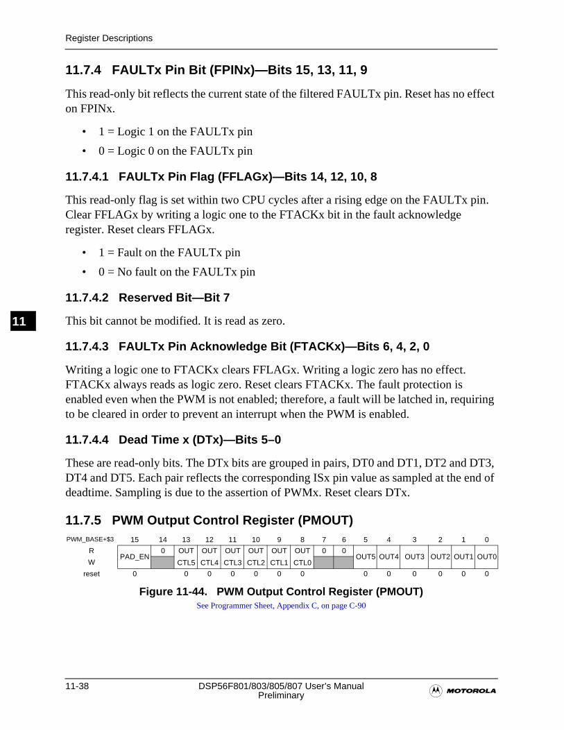
11-38 DSP56F801/803/805/807 User’s Manual�Preliminary
Register Descriptions
11
11.7.4 FAULTx Pin Bit (FPINx)—Bits 15, 13, 11, 9
This read-only bit reflects the current state of the filtered FAULTx pin. Reset has no effect on FPINx.
• 1 = Logic 1 on the FAULTx pin
• 0 = Logic 0 on the FAULTx pin
11.7.4.1 FAULTx Pin Flag (FFLAGx)—Bits 14, 12, 10, 8
This read-only flag is set within two CPU cycles after a rising edge on the FAULTx pin. Clear FFLAGx by writing a logic one to the FTACKx bit in the fault acknowledge register. Reset clears FFLAGx.
• 1 = Fault on the FAULTx pin
• 0 = No fault on the FAULTx pin
11.7.4.2 Reserved Bit—Bit 7
This bit cannot be modified. It is read as zero.
11.7.4.3 FAULTx Pin Acknowledge Bit (FTACKx)—Bits 6, 4, 2, 0
Writing a logic one to FTACKx clears FFLAGx. Writing a logic zero has no effect. FTACKx always reads as logic zero. Reset clears FTACKx. The fault protection is enabled even when the PWM is not enabled; therefore, a fault will be latched in, requiring to be cleared in order to prevent an interrupt when the PWM is enabled.
11.7.4.4 Dead Time x (DTx)—Bits 5–0
These are read-only bits. The DTx bits are grouped in pairs, DT0 and DT1, DT2 and DT3, DT4 and DT5. Each pair reflects the corresponding ISx pin value as sampled at the end of deadtime. Sampling is due to the assertion of PWMx. Reset clears DTx.
11.7.5 PWM Output Control Register (PMOUT)
Figure 11-44. PWM Output Control Register (PMOUT)See Programmer Sheet, Appendix C, on page C-90
PWM_BASE+$3 15 14 13 12 11 10 9 8 7 6 5 4 3 2 1 0
RPAD_EN
0 OUT
CTL5
OUT
CTL4
OUT
CTL3
OUT
CTL2
OUT
CTL1
OUT
CTL0
0 0OUT5 OUT4 OUT3 OUT2 OUT1 OUT0
W
reset 0 0 0 0 0 0 0 0 0 0 0 0 0
Register Descriptions
�Pulse Width Modulator Module (PWM) 11-39
Preliminary
11
11.7.5.1 Output Pad Enable (PAD_EN)—Bit 15
The PWMx output pads can be enabled or disabled by setting the PAD_EN bit. The power-up default has the pads disabled. This bit does not affect the functionality of the PWM, so the PWM module can be energized with the output pads disabled. The main reason for this enable is to power up with a safe default value for the PWM drivers.
• 1 = Output Pad enabled
• 0 = Output Pad disabled
11.7.5.2 Reserved Bits—Bits 14 and 7–6• These bits cannot be modified. They are read as zero.
11.7.5.3 Output Control Enables (OUTCTL5–0)—Bits 13–8
These read/write bits enable software control of their corresponding PWM pin. When OUTCTLx is set, the OUTx bit activates and deactivates the PWMx output. Reset clears the OUTCTL bits.
• 1 = Software control enabled
• 0 = Software control disabled
11.7.5.4 Output Control Bits (OUT5–0)—Bits 5–0
When the corresponding OUTCTL bit is set, these read/write bits control the PWM pins, illustrated in Table 11-8.

11-40 DSP56F801/803/805/807 User’s Manual�Preliminary
Register Descriptions
11
Table 11-8. Software Output Control
11.7.6 PWM Counter Register (PMCNT)
This read-only register displays the state of the 15-bit PWM counter. Reserved bit 15, cannot be modified. It is read as zero.
Figure 11-45. PWM Counter Register (PMCNT)See Programmer Sheet, Appendix C, on page C-90
11.7.7 PWM Counter Modulo Register (PWMCM)
The 15-bit unsigned value written to this buffered, read/write register is the PWM period in PWM clock periods. Reserved bit 15 cannot be modified. It is read as zero.
Note: The PWM counter modulo register is buffered. The value written does not take effect until the LDOK bit is set and the next PWM load cycle begins. Reading PWMCM reads the value in a buffer. It is not necessarily the value the PWM generator is currently using.
OUTx bit
Complementary channel operation Independent channel operation
OUT0 1—PWM0 is active0—PWM0 is inactive
1—PWM0 is active0—PWM0 is inactive
OUT1 1—PWM1 is complement of PWM 00—PWM1 is inactive
1—PWM1 is active0—PWM1 is inactive
OUT2 1—PWM2 is active0—PWM2 is inactive
1—PWM2 is active0—PWM2 is inactive
OUT3 1—PWM3 is complement of PWM 20—PWM3 is inactive
1—PWM3 is active0—PWM3 is inactive
OUT4 1—PWM4 is active0—PWM4 is inactive
1—PWM4 is active0—PWM4 is inactive
OUT5 1—PWM5is complement of PWM 40—PWM5 is inactive
1—PWM5 is active0—PWM5 is inactive
PWM_BASE+$4 15 14 13 12 11 10 9 8 7 6 5 4 3 2 1 0
R 0 CR[14:0]
W
reset 0 0 0 0 0 0 0 0 0 0 0 0 0 0 0
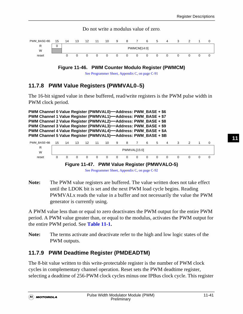
Register Descriptions
�Pulse Width Modulator Module (PWM) 11-41
Preliminary
11
Do not write a modulus value of zero.
Figure 11-46. PWM Counter Modulo Register (PWMCM)See Programmer Sheet, Appendix C, on page C-91
11.7.8 PWM Value Registers (PWMVAL0–5)
The 16-bit signed value in these buffered, read/write registers is the PWM pulse width in PWM clock period.
PWM Channel 0 Value Register (PWMVAL0)—Address: PWM_BASE + $6 PWM Channel 1 Value Register (PWMVAL1)—Address: PWM_BASE + $7PWM Channel 2 Value Register (PWMVAL2)—Address: PWM_BASE + $8PWM Channel 3 Value Register (PWMVAL3)—Address: PWM_BASE + $9PWM Channel 4 Value Register (PWMVAL4)—Address: PWM_BASE + $APWM Channel 5 Value Register (PWMVAL5)—Address: PWM_BASE + $B
Figure 11-47. PWM Value Register (PMWVALO-5)See Programmer Sheet, Appendix C, on page C-92
Note: The PWM value registers are buffered. The value written does not take effect until the LDOK bit is set and the next PWM load cycle begins. Reading PWMVALx reads the value in a buffer and not necessarily the value the PWM generator is currently using.
A PWM value less than or equal to zero deactivates the PWM output for the entire PWM period. A PWM value greater than, or equal to the modulus, activates the PWM output for the entire PWM period. See Table 11-1.
Note: The terms activate and deactivate refer to the high and low logic states of the PWM outputs.
11.7.9 PWM Deadtime Register (PMDEADTM)
The 8-bit value written to this write-protectable register is the number of PWM clock cycles in complementary channel operation. Reset sets the PWM deadtime register, selecting a deadtime of 256-PWM clock cycles minus one IPBus clock cycle. This register
PWM_BASE+$5 15 14 13 12 11 10 9 8 7 6 5 4 3 2 1 0
R 0PWMCM[14:0]
W
reset 0 0 0 0 0 0 0 0 0 0 0 0 0 0 0
PWM_BASE+$6 15 14 13 12 11 10 9 8 7 6 5 4 3 2 1 0
RPWMVAL[15:0]
W
reset 0 0 0 0 0 0 0 0 0 0 0 0 0 0 0 0
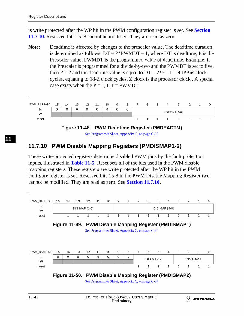
11-42 DSP56F801/803/805/807 User’s Manual�Preliminary
Register Descriptions
11
is write protected after the WP bit in the PWM configuration register is set. See Section 11.7.10. Reserved bits 15–8 cannot be modified. They are read as zero.
Note: Deadtime is affected by changes to the prescaler value. The deadtime duration is determined as follows: DT = P*PWMDT – 1, where DT is deadtime, P is the Prescaler value, PWMDT is the programmed value of dead time. Example: if the Prescaler is programmed for a divide-by-two and the PWMDT is set to five, then P = 2 and the deadtime value is equal to DT = 2*5 – 1 = 9 IPBus clock cycles, equating to 18-Z clock cycles. Z clock is the processor clock . A special case exists when the P = 1, DT = PWMDT
.
Figure 11-48. PWM Deadtime Register (PMDEADTM)See Programmer Sheet, Appendix C, on page C-93
11.7.10 PWM Disable Mapping Registers (PMDISMAP1-2)
These write-protected registers determine disabled PWM pins by the fault protection inputs, illustrated in Table 11-5. Reset sets all of the bits used in the PWM disable mapping registers. These registers are write protected after the WP bit in the PWM configure register is set. Reserved bits 15-8 in the PWM Disable Mapping Register two cannot be modified. They are read as zero. See Section 11.7.10.
.
Figure 11-49. PWM Disable Mapping Register (PMDISMAP1)See Programmer Sheet, Appendix C, on page C-94
Figure 11-50. PWM Disable Mapping Register (PMDISMAP2)See Programmer Sheet, Appendix C, on page C-94
PWM_BASE+$C 15 14 13 12 11 10 9 8 7 6 5 4 3 2 1 0
R 0 0 0 0 0 0 0 0PWMDT[7:0]
W
reset 1 1 1 1 1 1 1 1
PWM_BASE+$D 15 14 13 12 11 10 9 8 7 6 5 4 3 2 1 0
RDIS MAP [1-5] DIS MAP [9-0]
W
reset 1 1 1 1 1 1 1 1 1 1 1 1 1 1 1
PWM_BASE+$E 15 14 13 12 11 10 9 8 7 6 5 4 3 2 1 0
R 0 0 0 0 0 0 0 0DIS MAP 2 DIS MAP 1
W
reset 1 1 1 1 1 1 1 1
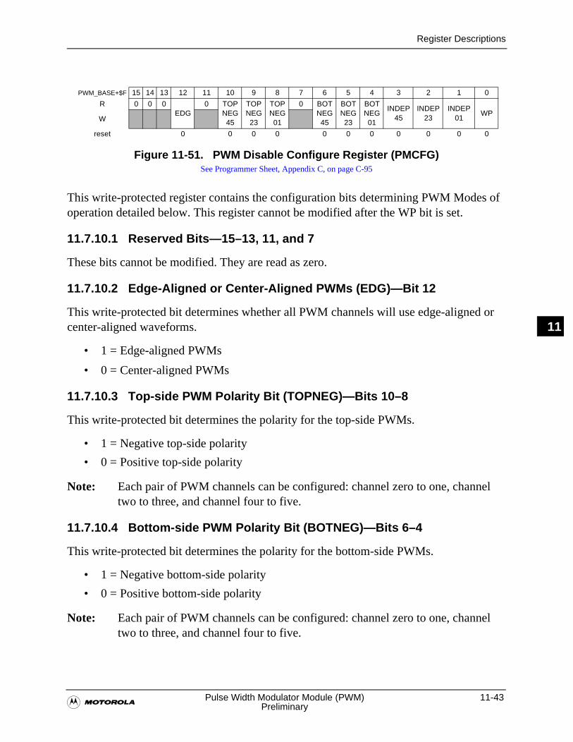
Register Descriptions
�Pulse Width Modulator Module (PWM) 11-43
Preliminary
11
Figure 11-51. PWM Disable Configure Register (PMCFG)See Programmer Sheet, Appendix C, on page C-95
This write-protected register contains the configuration bits determining PWM Modes of operation detailed below. This register cannot be modified after the WP bit is set.
11.7.10.1 Reserved Bits—15–13, 11, and 7
These bits cannot be modified. They are read as zero.
11.7.10.2 Edge-Aligned or Center-Aligned PWMs (EDG)—Bit 12
This write-protected bit determines whether all PWM channels will use edge-aligned or center-aligned waveforms.
• 1 = Edge-aligned PWMs
• 0 = Center-aligned PWMs
11.7.10.3 Top-side PWM Polarity Bit (TOPNEG)—Bits 10–8
This write-protected bit determines the polarity for the top-side PWMs.
• 1 = Negative top-side polarity
• 0 = Positive top-side polarity
Note: Each pair of PWM channels can be configured: channel zero to one, channel two to three, and channel four to five.
11.7.10.4 Bottom-side PWM Polarity Bit (BOTNEG)—Bits 6–4
This write-protected bit determines the polarity for the bottom-side PWMs.
• 1 = Negative bottom-side polarity
• 0 = Positive bottom-side polarity
Note: Each pair of PWM channels can be configured: channel zero to one, channel two to three, and channel four to five.
PWM_BASE+$F 15 14 13 12 11 10 9 8 7 6 5 4 3 2 1 0
R 0 0 0EDG
0 TOPNEG 45
TOPNEG 23
TOPNEG 01
0 BOTNEG 45
BOTNEG 23
BOTNEG 01
INDEP45
INDEP23
INDEP 01
WPW
reset 0 0 0 0 0 0 0 0 0 0 0
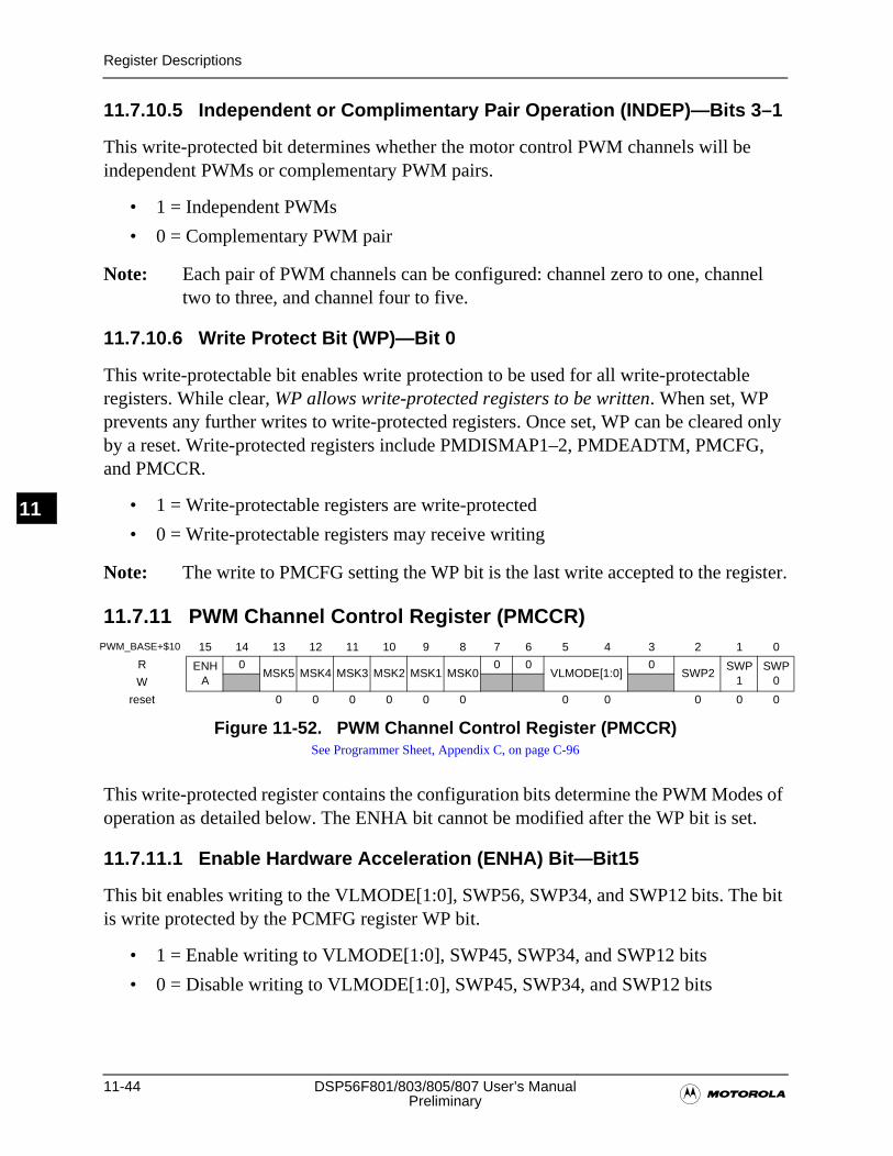
11-44 DSP56F801/803/805/807 User’s Manual�Preliminary
Register Descriptions
11
11.7.10.5 Independent or Complimentary Pair Operation (INDEP)—Bits 3–1
This write-protected bit determines whether the motor control PWM channels will be independent PWMs or complementary PWM pairs.
• 1 = Independent PWMs
• 0 = Complementary PWM pair
Note: Each pair of PWM channels can be configured: channel zero to one, channel two to three, and channel four to five.
11.7.10.6 Write Protect Bit (WP)—Bit 0
This write-protectable bit enables write protection to be used for all write-protectable registers. While clear, WP allows write-protected registers to be written. When set, WP prevents any further writes to write-protected registers. Once set, WP can be cleared only by a reset. Write-protected registers include PMDISMAP1–2, PMDEADTM, PMCFG, and PMCCR.
• 1 = Write-protectable registers are write-protected
• 0 = Write-protectable registers may receive writing
Note: The write to PMCFG setting the WP bit is the last write accepted to the register.
11.7.11 PWM Channel Control Register (PMCCR)
Figure 11-52. PWM Channel Control Register (PMCCR)See Programmer Sheet, Appendix C, on page C-96
This write-protected register contains the configuration bits determine the PWM Modes of operation as detailed below. The ENHA bit cannot be modified after the WP bit is set.
11.7.11.1 Enable Hardware Acceleration (ENHA) Bit—Bit15
This bit enables writing to the VLMODE[1:0], SWP56, SWP34, and SWP12 bits. The bit is write protected by the PCMFG register WP bit.
• 1 = Enable writing to VLMODE[1:0], SWP45, SWP34, and SWP12 bits
• 0 = Disable writing to VLMODE[1:0], SWP45, SWP34, and SWP12 bits
PWM_BASE+$10 15 14 13 12 11 10 9 8 7 6 5 4 3 2 1 0
R ENHA
0MSK5 MSK4 MSK3 MSK2 MSK1 MSK0
0 0VLMODE[1:0]
0SWP2
SWP1
SWP0W
reset 0 0 0 0 0 0 0 0 0 0 0
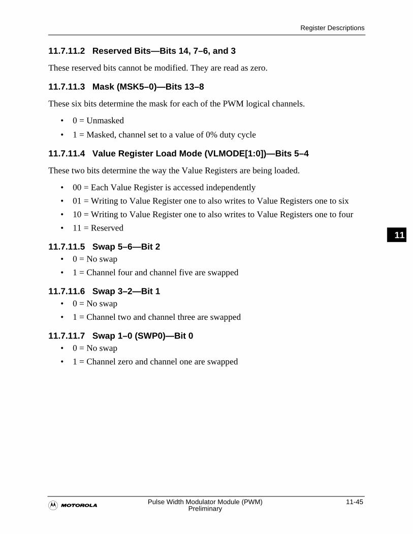
Register Descriptions
�Pulse Width Modulator Module (PWM) 11-45
Preliminary
11
11.7.11.2 Reserved Bits—Bits 14, 7–6, and 3
These reserved bits cannot be modified. They are read as zero.
11.7.11.3 Mask (MSK5–0)—Bits 13–8
These six bits determine the mask for each of the PWM logical channels.
• 0 = Unmasked
• 1 = Masked, channel set to a value of 0% duty cycle
11.7.11.4 Value Register Load Mode (VLMODE[1:0])—Bits 5–4
These two bits determine the way the Value Registers are being loaded.
• 00 = Each Value Register is accessed independently
• 01 = Writing to Value Register one to also writes to Value Registers one to six
• 10 = Writing to Value Register one to also writes to Value Registers one to four
• 11 = Reserved
11.7.11.5 Swap 5–6—Bit 2• 0 = No swap
• 1 = Channel four and channel five are swapped
11.7.11.6 Swap 3–2—Bit 1• 0 = No swap
• 1 = Channel two and channel three are swapped
11.7.11.7 Swap 1–0 (SWP0)—Bit 0• 0 = No swap
• 1 = Channel zero and channel one are swapped
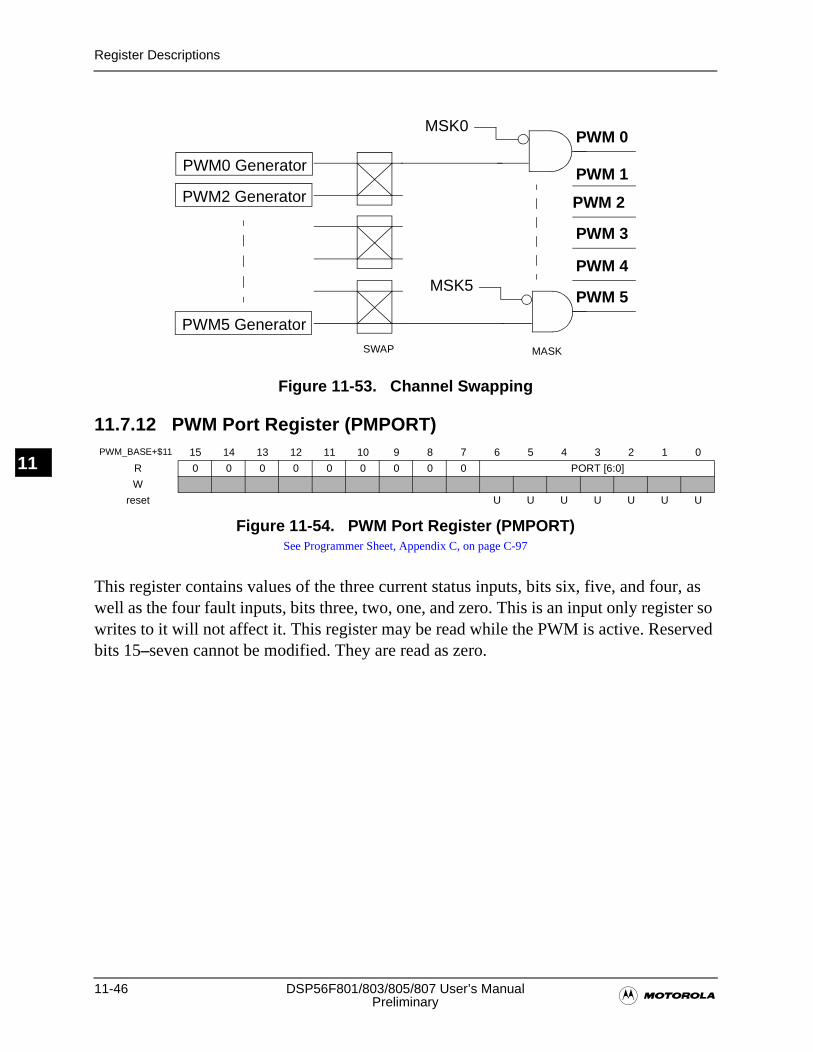
11-46 DSP56F801/803/805/807 User’s Manual�Preliminary
Register Descriptions
11
Figure 11-53. Channel Swapping
11.7.12 PWM Port Register (PMPORT)
Figure 11-54. PWM Port Register (PMPORT)See Programmer Sheet, Appendix C, on page C-97
This register contains values of the three current status inputs, bits six, five, and four, as well as the four fault inputs, bits three, two, one, and zero. This is an input only register so writes to it will not affect it. This register may be read while the PWM is active. Reserved bits 15–seven cannot be modified. They are read as zero.
PWM_BASE+$11 15 14 13 12 11 10 9 8 7 6 5 4 3 2 1 0
R 0 0 0 0 0 0 0 0 0 PORT [6:0]
W
reset U U U U U U U
PWM 0
PWM 1
PWM 2
PWM 3
PWM 4
PWM 5
PWM0 Generator
PWM2 Generator
MSK0
PWM5 Generator
MSK5
SWAP MASK
�Serial Communications Interface Module (SCI) 12-1
Preliminary
12
Chapter 12Serial Communications Interface
Module (SCI)

12-2 DSP56F801/803/805/807 User’s Manual�Preliminary
12
Features
�Serial Communications Interface Module (SCI) 12-3
Preliminary
12
12.1 Introduction
This chapter describes the Serial Communications Interface module, allowing asynchronous serial communications with peripheral devices and other MCUs. The DSP56F801/803 have a single interface: SCI0, while DSP56F805/807 have two interfaces: SCI0 and SCI1. This chapter describes the Serial Communications Interface module.
12.2 Features• Full duplex or single wire operation
• Standard mark/space non-return-to-zero (NRZ) format
• 13-bit baud rate selection
• Programmable 8-bit or 9-bit data format
• Separately enabled transmitter and receiver
• Separate receiver and transmitter CPU interrupt requests
• Programmable polarity for transmitter and receiver
• Two receiver wake-up methods: idle line or address mark
• Interrupt-driven operation with eight flags:
— Transmitter empty
— Transmitter idle
— Receiver full
— Receiver idle
— Receiver overrun
— Noise error
— Framing error
— Parity error
• Receiver framing error detection
• Hardware parity checking
• 1/16 bit-time noise detection•
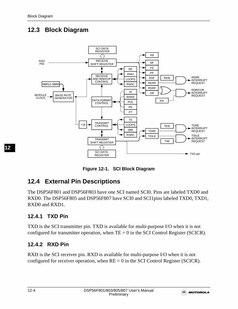
12-4 DSP56F801/803/805/807 User’s Manual�Preliminary
Block Diagram
12
12.3 Block Diagram
Figure 12-1. SCI Block Diagram
12.4 External Pin Descriptions
The DSP56F801 and DSP56F803 have one SCI named SCI0. Pins are labeled TXD0 and RXD0. The DSP56F805 and DSP56F807 have SCI0 and SCI1pins labeled TXD0, TXD1, RXD0 and RXD1.
12.4.1 TXD Pin
TXD is the SCI transmitter pin. TXD is available for multi-purpose I/O when it is not configured for transmitter operation, when TE = 0 in the SCI Control Register (SCICR).
12.4.2 RXD Pin
RXD is the SCI receiver pin. RXD is available for multi-purpose I/O when it is not configured for receiver operation, when RE = 0 in the SCI Control Register (SCICR).
SCI DATA
RECEIVESHIFT REGISTER
SCI DATA REGISTER
TRANSMITSHIFT REGISTER
REGISTER
BAUD RATEGENERATOR
SBR12–SBR0
RXD
TXD pin
MODULE
TRANSMITCONTROL÷16
RECEIVEAND WAKEUP
DATA FORMATCONTROL
CONTROL
PF
FE
NF
RDRF
RERR
TEIE
OR
TIIE
TDRE
TIDLE
R8
RAFLOOPS
RWU
RE
PE
POL
PT
WAKE
M
CLOCK
RERRREIE
RIE
RDRF/OR
TDRE
TIDLE
INTERRUPT
INTERRUPT
INTERRUPT
INTERRUPT
PIN
RSRC
SBK
LOOPS
TE
RSRCREQUEST
REQUEST
REQUEST
REQUEST
Functional Description
�Serial Communications Interface Module (SCI) 12-5
Preliminary
12
12.5 Register Summary
A prefix is added to each register reflecting SCI module is being accessed: SCI0 or SCI1. For example, the SCIBR for the SCI0 module will be called SCI0_SCIBR.
Each DSP56F801/803/805/807 serial communications interface has the following registers:
• SCI Baud Rate Register (SCIBR)
• SCI Control Register (SCICR)
• SCI Status Register (SCISR)
• SCI Data Register (SCIDR)
For more information concerning SCI0 registers address map please refer to Table 3-26. For SCI1 registers address map, please refer to Table 3-27.
12.6 Definition of Terms
A character consists of eight or nine bits of data. A frame consists of a start bit, followed by a character, followed by a stop bit. The character in a frame may have a parity bit inserted into it. A message consists of multiple frames. Messages are separated by preambles, each consisting of 10 or 11 bits of idle line, logic 1. Within a message, care should be taken assuring the idle time between frames is kept to a minimum so the receiver doesn’t see a false preamble. Queuing up the next character while the current frame is being transmitted assures minimal idle time between frames.
12.7 Functional Description
Figure 12-1 illustrates the structure of the SCI module. The SCI allows full duplex, asynchronous, NRZ serial communication between the MCU and remote devices, including other MCUs. The SCI transmitter and receiver operate independently, although they use the same baud rate generator. The CPU monitors the status of the SCI, writes the data to be transmitted, and processes received data.
When initializing the SCI, be sure to set the proper peripheral enable bits in the MPIO, as well as any pull-up enables.
12.7.1 Data Frame Format
The SCI uses the standard NRZ mark/space data frame format illustrated in Figure 12-2.
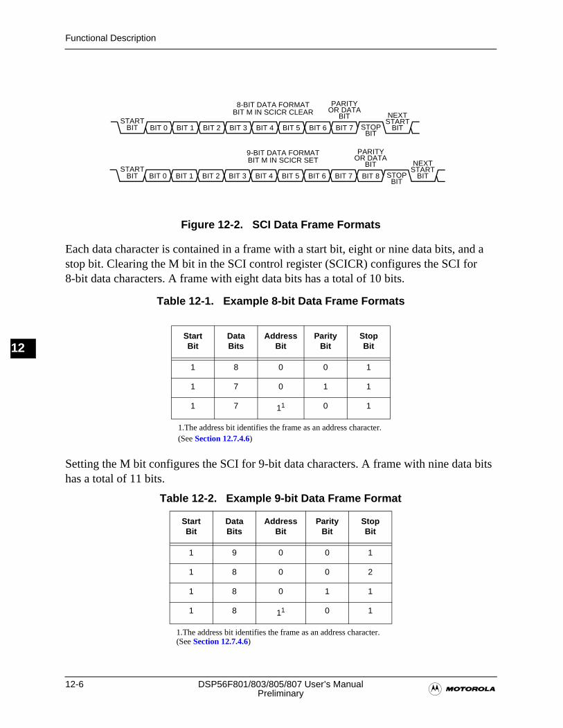
12-6 DSP56F801/803/805/807 User’s Manual�Preliminary
Functional Description
12
Figure 12-2. SCI Data Frame Formats
Each data character is contained in a frame with a start bit, eight or nine data bits, and a stop bit. Clearing the M bit in the SCI control register (SCICR) configures the SCI for 8-bit data characters. A frame with eight data bits has a total of 10 bits.
Table 12-1. Example 8-bit Data Frame Formats
Setting the M bit configures the SCI for 9-bit data characters. A frame with nine data bits has a total of 11 bits.
StartBit
DataBits
AddressBit
ParityBit
StopBit
1 8 0 0 1
1 7 0 1 1
1 7 11
1.The address bit identifies the frame as an address character. (See Section 12.7.4.6)
0 1
Table 12-2. Example 9-bit Data Frame Format
StartBit
DataBits
AddressBit
ParityBit
StopBit
1 9 0 0 1
1 8 0 0 2
1 8 0 1 1
1 8 11
1.The address bit identifies the frame as an address character. (See Section 12.7.4.6)
0 1
BIT 5START
BIT BIT 0 BIT 1
NEXT
STOPBIT
STARTBIT
9-BIT DATA FORMAT
BIT 2 BIT 3 BIT 4 BIT 6 BIT 7
PARITYOR DATA
BIT
PARITYOR DATA
BIT
BIT M IN SCICR SET
8-BIT DATA FORMATBIT M IN SCICR CLEAR
BIT 5BIT 0 BIT 1 BIT 2 BIT 3 BIT 4 BIT 6 BIT 7 BIT 8 STOPBIT
NEXTSTART
BITSTART
BIT
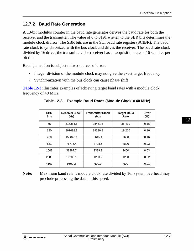
Functional Description
�Serial Communications Interface Module (SCI) 12-7
Preliminary
12
12.7.2 Baud Rate Generation
A 13-bit modulus counter in the baud rate generator derives the baud rate for both the receiver and the transmitter. The value of 0 to 8191 written to the SBR bits determines the module clock divisor. The SBR bits are in the SCI baud rate register (SCIBR). The baud rate clock is synchronized with the bus clock and drives the receiver. The baud rate clock divided by 16 drives the transmitter. The receiver has an acquisition rate of 16 samples per bit time.
Baud generation is subject to two sources of error:
• Integer division of the module clock may not give the exact target frequency
• Synchronization with the bus clock can cause phase shift
Table 12-3 illustrates examples of achieving target baud rates with a module clock frequency of 40 MHz.
Table 12-3. Example Baud Rates (Module Clock = 40 MHz)
Note: Maximum baud rate is module clock rate divided by 16. System overhead may preclude processing the data at this speed.
SBR Bits
Receiver Clock (Hz)
Transmitter Clock (Hz)
Target Baud Rate
Error (%)
65 615384.6 38461.5 38,400 0.16
130 307692.3 19230.8 19,200 0.16
260 153846.1 9615.4 9600 0.16
521 76775.4 4798.5 4800 0.03
1042 38387.7 2399.2 2400 0.03
2083 19203.1 1200.2 1200 0.02
4167 9599.2 600.0 600 0.01
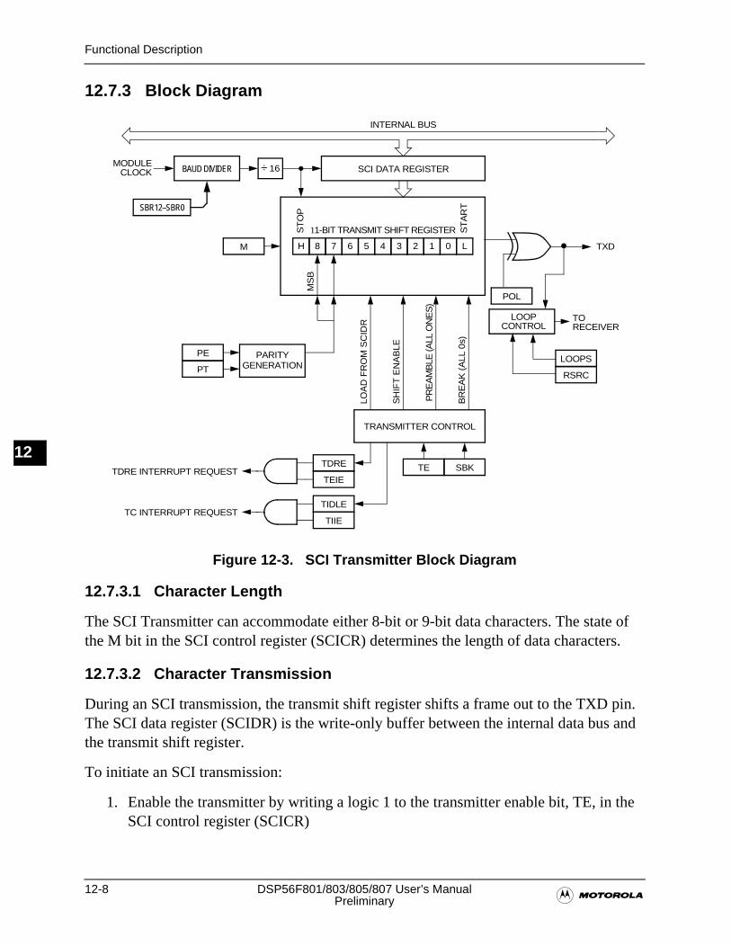
12-8 DSP56F801/803/805/807 User’s Manual�Preliminary
Functional Description
12
12.7.3 Block Diagram
Figure 12-3. SCI Transmitter Block Diagram
12.7.3.1 Character Length
The SCI Transmitter can accommodate either 8-bit or 9-bit data characters. The state of the M bit in the SCI control register (SCICR) determines the length of data characters.
12.7.3.2 Character Transmission
During an SCI transmission, the transmit shift register shifts a frame out to the TXD pin. The SCI data register (SCIDR) is the write-only buffer between the internal data bus and the transmit shift register.
To initiate an SCI transmission:
1. Enable the transmitter by writing a logic 1 to the transmitter enable bit, TE, in the SCI control register (SCICR)
PE
PT
H 8 7 6 5 4 3 2 1 0 L
11-BIT TRANSMIT SHIFT REGISTERST
OP
ST
AR
TTDRE
TEIE
TIIE
SBK
TIDLE
PARITYGENERATION
MS
B
SCI DATA REGISTER
LOA
D F
RO
M S
CID
R
SH
IFT
EN
AB
LE
PR
EA
MB
LE (A
LL O
NE
S)
BR
EA
K (
ALL
0s)
TRANSMITTER CONTROL
M
INTERNAL BUS
SBR12–SBR0
BAUD DIVIDER ÷ 16
TXD
TDRE INTERRUPT REQUEST
TC INTERRUPT REQUEST
MODULE
LOOP
LOOPS
RSRC
CLOCK
TE
TOCONTROL RECEIVER
POL
Functional Description
�Serial Communications Interface Module (SCI) 12-9
Preliminary
12
2. Clear the transmit data register empty flag, TDRE, by first reading the SCI status register (SCISR) and then writing to the SCI data register (SCIDR)
3. Repeat step two for each subsequent transmission
Writing the TE bit from 0 to a 1 automatically loads the transmit shift register with a preamble of 10 logic 1s (if M = 0) or 11 logic 1s (if M = 1). After the preamble shifts out, control logic automatically transfers the data from the SCI data register into the transmit shift register. A logic zero start bit automatically goes into the LSB position of the transmit shift register. A logic one stop bit goes into the MSB position of the frame.
Hardware supports odd or even parity. When parity is enabled, the MSB of the data character is replaced by the parity bit.
The transmit data register empty flag, TDRE, in the SCI status register (SCISR) becomes set when the SCI data register transfers a character to the transmit shift register. The TDRE flag indicates the SCIDR can accept new data from the internal data bus. If the transmitter empty interrupt enable bit, TEIE, in the SCICR is also set, the TDRE flag generates a transmitter interrupt request.
When the transmit shift register is not transmitting a frame and TE = 1, the TXD pin goes to the idle condition, logic one. If at any time software clears the TE bit in the SCICR, the transmitter relinquishes control of the port I/O pin upon completion of the current transmission, causing the TXD pin to go to a high impedance state.
If software clears TE while a transmission is in progress (TIDLE = 0), the frame in the transmit shift register continues to shift out. Then transmission stops even if there is data pending in the SCI data register. To avoid accidentally cutting off the last frame in a message, always wait for TDRE to go high after the last frame before clearing TE.
To separate messages having preambles with minimum idle line time, use this sequence between messages:
1. Write the last character of the first message to SCIDR
2. Wait for the TDRE flag to go high, indicating the transfer of the last frame to the transmit shift register
3. Queue a preamble by clearing and then setting the TE bit
4. Write the first character of the second message to SCIDR
12-10 DSP56F801/803/805/807 User’s Manual�Preliminary
Functional Description
12
12.7.3.3 Break Characters
Writing a logic one to the send break bit, SBK, in the SCICR loads the transmit shift register with a break character. A break character contains all logic zeros and has no start, stop, or parity bit. Break character length depends on the M bit in the SCICR. As long as SBK is at logic one, transmitter logic continuously loads break characters into the transmit shift register. After software clears the SBK bit, the shift register finishes transmitting the last break character and then transmits at least one logic one. The automatic logic one at the end of the last break character guarantees the recognition of the start bit of the next frame.
The SCI recognizes a break character when a start bit is followed by eight or nine logic one data bits and a logic 0 where the stop bit should be. Receiving a break character has these effects on SCI registers:
• Sets the framing error flag, FE
• Sets the receive data register full flag, RDRF
• Clears the SCI data register (SCIDR)
• May set the overrun flag, OR, noise flag, NF, parity error flag, PE, or the receiver active flag, RAF. See Section 12.8.3
12.7.3.4 Preambles
A preamble contains all logic ones and has no start, stop, or parity bit. Preamble length depends on the M bit in the SCICR. The preamble is a synchronizing mechanism beginning the first transmission initiated after writing the TE bit from zero to one.
If the TE bit is cleared during a transmission, the TXD pin becomes idle after completion of the transmission in progress. Clearing and then setting the TE bit during a transmission queues a preamble to be sent after the frame currently being transmitted.
Note: Toggle the TE bit for a queued preamble when the TDRE flag becomes set and immediately before writing the next character to the SCIDR.
When queueing a preamble, return the TE bit to logic 1 before the stop bit of the current frame shifts out to the TXD pin. Setting TE after the stop bit appears on TXD causes data previously written to the SCIDR to be lost.
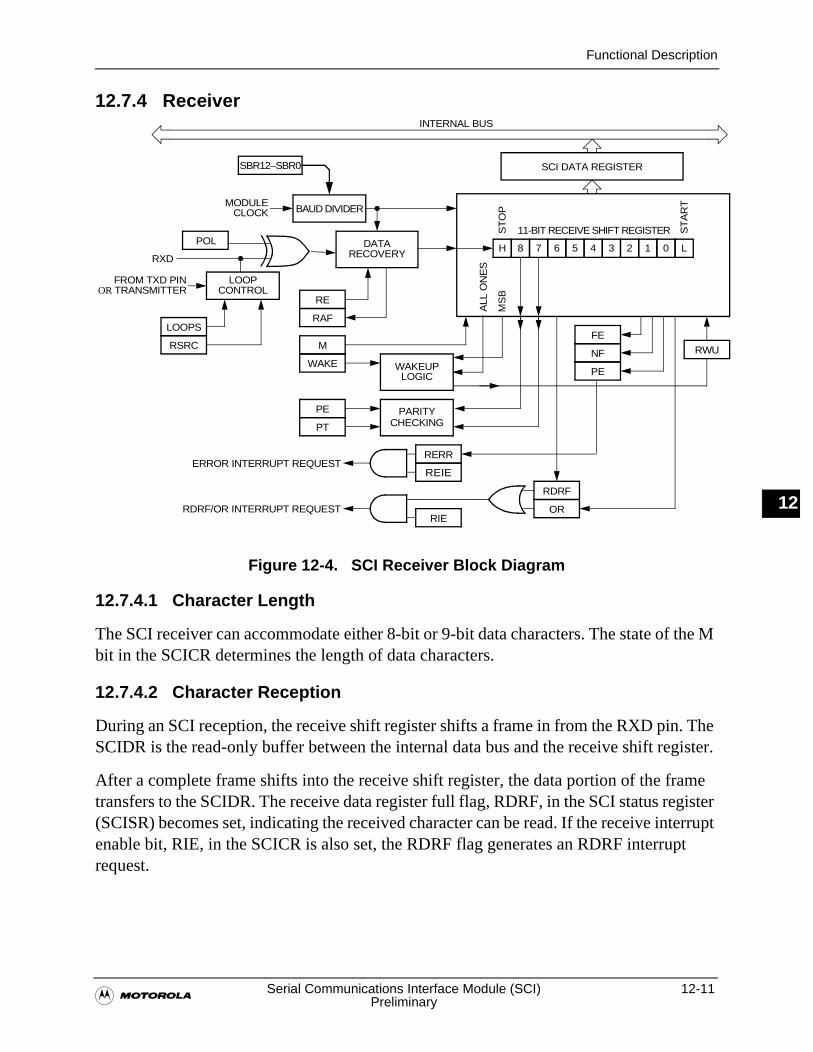
Functional Description
�Serial Communications Interface Module (SCI) 12-11
Preliminary
12
12.7.4 Receiver
Figure 12-4. SCI Receiver Block Diagram
12.7.4.1 Character Length
The SCI receiver can accommodate either 8-bit or 9-bit data characters. The state of the M bit in the SCICR determines the length of data characters.
12.7.4.2 Character Reception
During an SCI reception, the receive shift register shifts a frame in from the RXD pin. The SCIDR is the read-only buffer between the internal data bus and the receive shift register.
After a complete frame shifts into the receive shift register, the data portion of the frame transfers to the SCIDR. The receive data register full flag, RDRF, in the SCI status register (SCISR) becomes set, indicating the received character can be read. If the receive interrupt enable bit, RIE, in the SCICR is also set, the RDRF flag generates an RDRF interrupt request.
ALL
ON
ES
M
WAKE
PE
PT
RE
H 8 7 6 5 4 3 2 1 0 L
11-BIT RECEIVE SHIFT REGISTERST
OP
ST
AR
T
DATA
WAKEUP
PARITYCHECKING
MS
B
SCI DATA REGISTER
RIE
REIE
RWU
RDRF
OR
NF
FE
PE
INTERNAL BUS
RXD
MODULE
ERROR INTERRUPT REQUEST
RDRF/OR INTERRUPT REQUEST
SBR12–SBR0
BAUD DIVIDER
LOOP
LOOPS
RSRC
FROM TXD PINOR TRANSMITTER
CLOCK
RERR
RAF
RECOVERY
CONTROL
LOGIC
POL
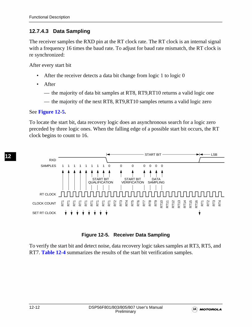
12-12 DSP56F801/803/805/807 User’s Manual�Preliminary
Functional Description
12
12.7.4.3 Data Sampling
The receiver samples the RXD pin at the RT clock rate. The RT clock is an internal signal with a frequency 16 times the baud rate. To adjust for baud rate mismatch, the RT clock is re synchronized:
After every start bit
• After the receiver detects a data bit change from logic 1 to logic 0
• After
— the majority of data bit samples at RT8, RT9,RT10 returns a valid logic one
— the majority of the next RT8, RT9,RT10 samples returns a valid logic zero
See Figure 12-5.
To locate the start bit, data recovery logic does an asynchronous search for a logic zero preceded by three logic ones. When the falling edge of a possible start bit occurs, the RT clock begins to count to 16.
Figure 12-5. Receiver Data Sampling
To verify the start bit and detect noise, data recovery logic takes samples at RT3, RT5, and RT7. Table 12-4 summarizes the results of the start bit verification samples.
ESET RT CLOCK
RT
1
RT
1
RT
1
RT
1
RT
1
RT
1
RT
1
RT
1
RT
1
RT
2
RT
3
RT
4
RT
5
RT
8
RT
7
RT
6
RT
11
RT
10
RT
9
RT
15
RT
14
RT
13
RT
12
RT
16
RT
1
RT
2
RT
3
RT
4
SAMPLES
RT CLOCK
CLOCK COUNT
START BIT
RXD
START BITQUALIFICATION
START BIT DATASAMPLING
1 111111 1 0 0 0 000 0
LSB
VERIFICATION
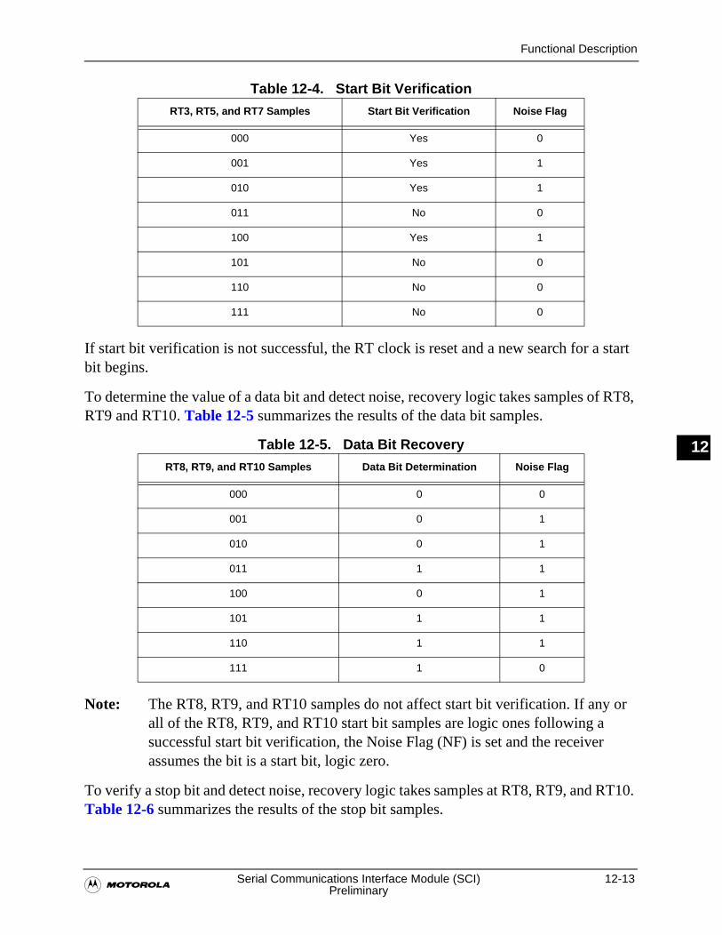
Functional Description
�Serial Communications Interface Module (SCI) 12-13
Preliminary
12
Table 12-4. Start Bit Verification
If start bit verification is not successful, the RT clock is reset and a new search for a start bit begins.
To determine the value of a data bit and detect noise, recovery logic takes samples of RT8, RT9 and RT10. Table 12-5 summarizes the results of the data bit samples.
Table 12-5. Data Bit Recovery
Note: The RT8, RT9, and RT10 samples do not affect start bit verification. If any or all of the RT8, RT9, and RT10 start bit samples are logic ones following a successful start bit verification, the Noise Flag (NF) is set and the receiver assumes the bit is a start bit, logic zero.
To verify a stop bit and detect noise, recovery logic takes samples at RT8, RT9, and RT10. Table 12-6 summarizes the results of the stop bit samples.
RT3, RT5, and RT7 Samples Start Bit Verification Noise Flag
000 Yes 0
001 Yes 1
010 Yes 1
011 No 0
100 Yes 1
101 No 0
110 No 0
111 No 0
RT8, RT9, and RT10 Samples Data Bit Determination Noise Flag
000 0 0
001 0 1
010 0 1
011 1 1
100 0 1
101 1 1
110 1 1
111 1 0
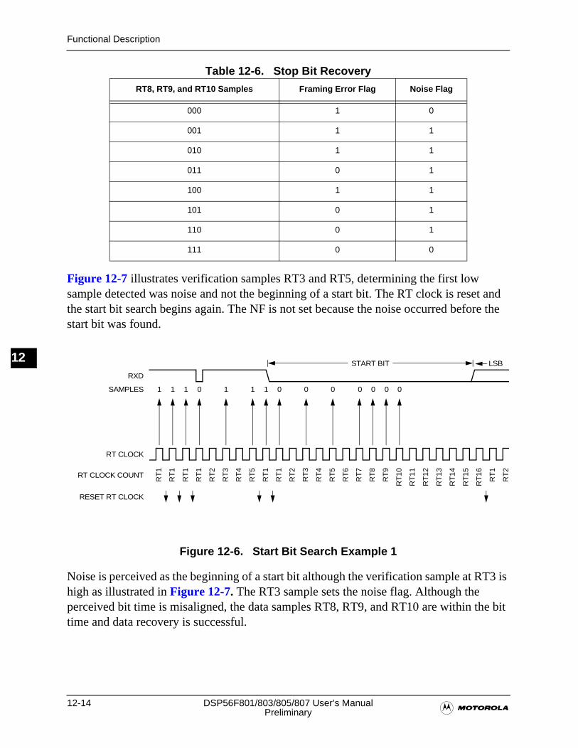
12-14 DSP56F801/803/805/807 User’s Manual�Preliminary
Functional Description
12
Table 12-6. Stop Bit Recovery
Figure 12-7 illustrates verification samples RT3 and RT5, determining the first low sample detected was noise and not the beginning of a start bit. The RT clock is reset and the start bit search begins again. The NF is not set because the noise occurred before the start bit was found.
Figure 12-6. Start Bit Search Example 1
Noise is perceived as the beginning of a start bit although the verification sample at RT3 is high as illustrated in Figure 12-7. The RT3 sample sets the noise flag. Although the perceived bit time is misaligned, the data samples RT8, RT9, and RT10 are within the bit time and data recovery is successful.
RT8, RT9, and RT10 Samples Framing Error Flag Noise Flag
000 1 0
001 1 1
010 1 1
011 0 1
100 1 1
101 0 1
110 0 1
111 0 0
RESET RT CLOCK
RT
1
RT
1
RT
1
RT
1
RT
2
RT
3
RT
4
RT
5
RT
1
RT
1
RT
2
RT
3
RT
4
RT
7
RT
6
RT
5
RT
10
RT
9
RT
8
RT
14
RT
13
RT
12
RT
11
RT
15
RT
16
RT
1
RT
2
SAMPLES
RT CLOCK
RT CLOCK COUNT
START BIT
RXD
1 1011 1 1 0 0 00 0
LSB
0 0
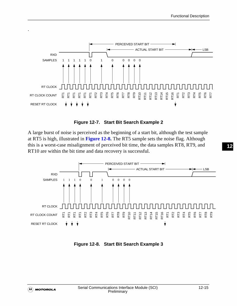
Functional Description
�Serial Communications Interface Module (SCI) 12-15
Preliminary
12
.
Figure 12-7. Start Bit Search Example 2
A large burst of noise is perceived as the beginning of a start bit, although the test sample at RT5 is high, illustrated in Figure 12-8. The RT5 sample sets the noise flag. Although this is a worst-case misalignment of perceived bit time, the data samples RT8, RT9, and RT10 are within the bit time and data recovery is successful.
Figure 12-8. Start Bit Search Example 3
RESET RT CLOCK
RT
1
RT
1
RT
1
RT
1
RT
1
RT
1
RT
2
RT
3
RT
4
RT
5
RT
6
RT
7
RT
8
RT
11
RT
10
RT
9
RT
14
RT
13
RT
12
RT
2
RT
1
RT
16
RT
15
RT
3
RT
4
RT
5
RT
6
RT
7
SAMPLES
RT CLOCK
RT CLOCK COUNT
ACTUAL START BIT
RXD
1 1111 1 0 0 00
LSB
00
PERCEIVED START BIT
RESET RT CLOCK
RT
1
RT
1
RT
1
RT
1
RT
2
RT
3
RT
4
RT
5
RT
6
RT
7
RT
8
RT
9
RT
10
RT
13
RT
12
RT
11
RT
16
RT
15
RT
14
RT
4
RT
3
RT
2
RT
1
RT
5
RT
6
RT
7
RT
8
RT
9
SAMPLES
RT CLOCK
RT CLOCK COUNT
ACTUAL START BIT
RXD
1 011 1 0 0 00
LSB
0
PERCEIVED START BIT
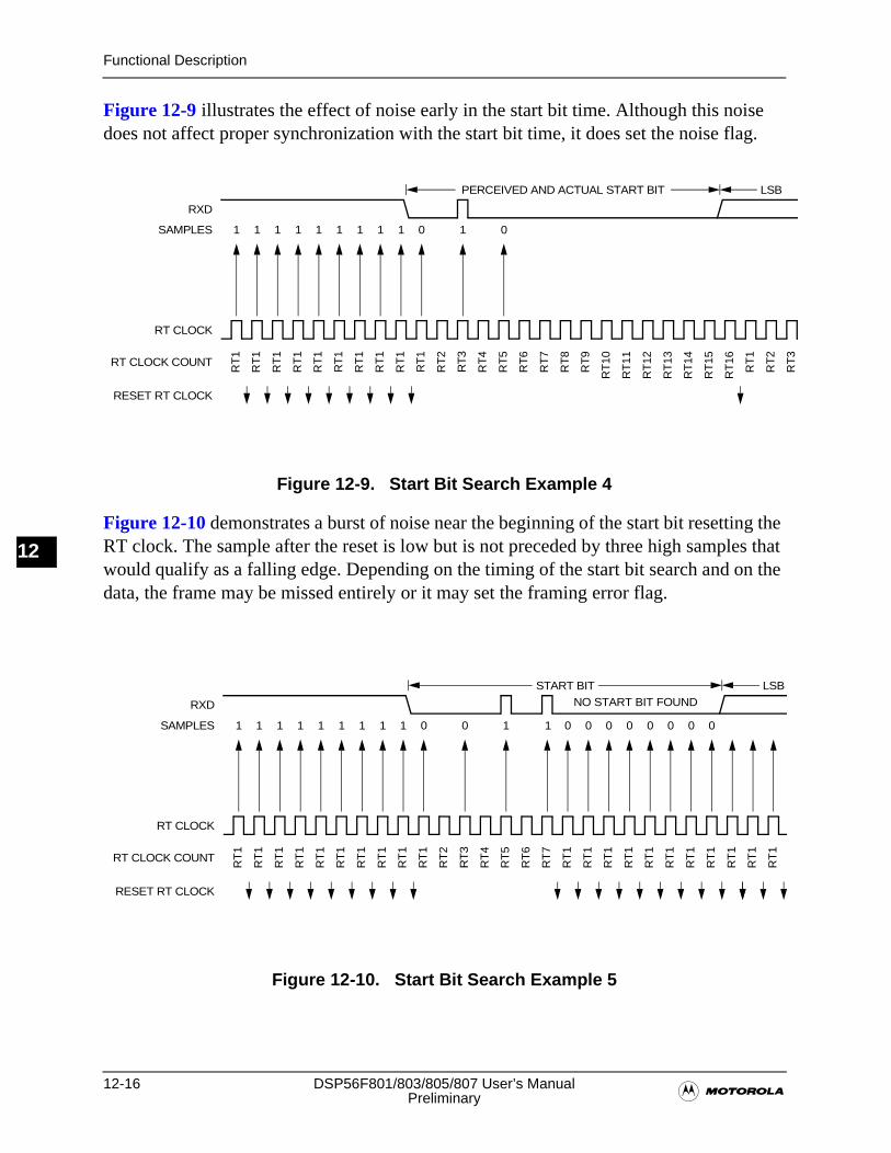
12-16 DSP56F801/803/805/807 User’s Manual�Preliminary
Functional Description
12
Figure 12-9 illustrates the effect of noise early in the start bit time. Although this noise does not affect proper synchronization with the start bit time, it does set the noise flag.
Figure 12-9. Start Bit Search Example 4
Figure 12-10 demonstrates a burst of noise near the beginning of the start bit resetting the RT clock. The sample after the reset is low but is not preceded by three high samples that would qualify as a falling edge. Depending on the timing of the start bit search and on the data, the frame may be missed entirely or it may set the framing error flag.
Figure 12-10. Start Bit Search Example 5
RESET RT CLOCK
RT
1
RT
1
RT
1
RT
1
RT
1
RT
1
RT
1
RT
1
RT
1
RT
1
RT
2
RT
3
RT
4
RT
7
RT
6
RT
5
RT
10
RT
9
RT
8
RT
14
RT
13
RT
12
RT
11
RT
15
RT
16
RT
1
RT
2
RT
3
SAMPLES
RT CLOCK
RT CLOCK COUNT
PERCEIVED AND ACTUAL START BIT
RXD
1 111 1 0 01
LSB
11 1 1
RESET RT CLOCK
RT
1
RT
1
RT
1
RT
1
RT
1
RT
1
RT
1
RT
1
RT
1
RT
1
RT
2
RT
3
RT
4
RT
7
RT
6
RT
5
RT
1
RT
1
RT
1
RT
1
RT
1
RT
1
RT
1
RT
1
RT
1
RT
1
RT
1
SAMPLES
RT CLOCK
RT CLOCK COUNT
START BIT
RXD
1 111 1 0 10
LSB
11 1 1 1 0 000 000 0
NO START BIT FOUND
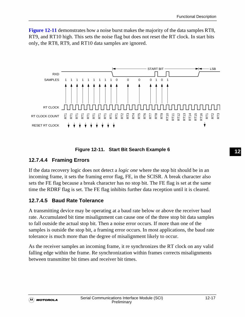
Functional Description
�Serial Communications Interface Module (SCI) 12-17
Preliminary
12
Figure 12-11 demonstrates how a noise burst makes the majority of the data samples RT8, RT9, and RT10 high. This sets the noise flag but does not reset the RT clock. In start bits only, the RT8, RT9, and RT10 data samples are ignored.
Figure 12-11. Start Bit Search Example 6
12.7.4.4 Framing Errors
If the data recovery logic does not detect a logic one where the stop bit should be in an incoming frame, it sets the framing error flag, FE, in the SCISR. A break character also sets the FE flag because a break character has no stop bit. The FE flag is set at the same time the RDRF flag is set. The FE flag inhibits further data reception until it is cleared.
12.7.4.5 Baud Rate Tolerance
A transmitting device may be operating at a baud rate below or above the receiver baud rate. Accumulated bit time misalignment can cause one of the three stop bit data samples to fall outside the actual stop bit. Then a noise error occurs. If more than one of the samples is outside the stop bit, a framing error occurs. In most applications, the baud rate tolerance is much more than the degree of misalignment likely to occur.
As the receiver samples an incoming frame, it re synchronizes the RT clock on any valid falling edge within the frame. Re synchronization within frames corrects misalignments between transmitter bit times and receiver bit times.
RESET RT CLOCK
RT
1
RT
1
RT
1
RT
1
RT
1
RT
1
RT
1
RT
1
RT
1
RT
1
RT
2
RT
3
RT
4
RT
7
RT
6
RT
5
RT
10
RT
9
RT
8
RT
14
RT
13
RT
12
RT
11
RT
15
RT
16
RT
1
RT
2
RT
3
SAMPLES
RT CLOCK
RT CLOCK COUNT
START BIT
RXD
1 111 1 0 00
LSB
11 1 1 0 1 10
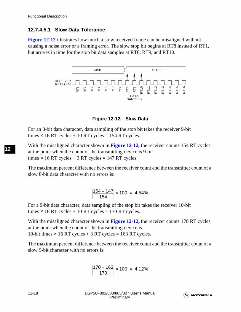
12-18 DSP56F801/803/805/807 User’s Manual�Preliminary
Functional Description
12
12.7.4.5.1 Slow Data Tolerance
Figure 12-12 illustrates how much a slow received frame can be misaligned without causing a noise error or a framing error. The slow stop bit begins at RT8 instead of RT1, but arrives in time for the stop bit data samples at RT8, RT9, and RT10.
Figure 12-12. Slow Data
For an 8-bit data character, data sampling of the stop bit takes the receiver 9-bit times × 16 RT cycles + 10 RT cycles = 154 RT cycles.
With the misaligned character shown in Figure 12-12, the receiver counts 154 RT cycles at the point when the count of the transmitting device is 9-bit times × 16 RT cycles + 3 RT cycles = 147 RT cycles.
The maximum percent difference between the receiver count and the transmitter count of a slow 8-bit data character with no errors is:
For a 9-bit data character, data sampling of the stop bit takes the receiver 10-bit times × 16 RT cycles + 10 RT cycles = 170 RT cycles.
With the misaligned character shown in Figure 12-12, the receiver counts 170 RT cycles at the point when the count of the transmitting device is10-bit times × 16 RT cycles + 3 RT cycles = 163 RT cycles.
The maximum percent difference between the receiver count and the transmitter count of a slow 9-bit character with no errors is:
MSB STOP
RT
1
RT
2
RT
3
RT
4
RT
5
RT
6
RT
7
RT
8
RT
9
RT
10
RT
11
RT
12
RT
13
RT
14
RT
15
RT
16
DATASAMPLES
RECEIVERRT CLOCK
154 147–154
-------------------------- 100× 4.54%=
170 163–170
-------------------------- 100× 4.12%=
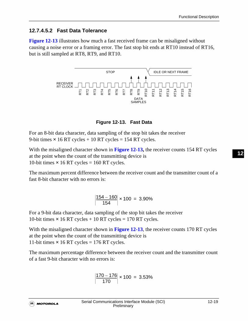
Functional Description
�Serial Communications Interface Module (SCI) 12-19
Preliminary
12
12.7.4.5.2 Fast Data Tolerance
Figure 12-13 illustrates how much a fast received frame can be misaligned without causing a noise error or a framing error. The fast stop bit ends at RT10 instead of RT16, but is still sampled at RT8, RT9, and RT10.
Figure 12-13. Fast Data
For an 8-bit data character, data sampling of the stop bit takes the receiver 9-bit times × 16 RT cycles + 10 RT cycles = 154 RT cycles.
With the misaligned character shown in Figure 12-13, the receiver counts 154 RT cycles at the point when the count of the transmitting device is 10-bit times × 16 RT cycles = 160 RT cycles.
The maximum percent difference between the receiver count and the transmitter count of a fast 8-bit character with no errors is:
For a 9-bit data character, data sampling of the stop bit takes the receiver 10-bit times × 16 RT cycles + 10 RT cycles = 170 RT cycles.
With the misaligned character shown in Figure 12-13, the receiver counts 170 RT cycles at the point when the count of the transmitting device is 11-bit times × 16 RT cycles = 176 RT cycles.
The maximum percentage difference between the receiver count and the transmitter count of a fast 9-bit character with no errors is:
IDLE OR NEXT FRAMESTOP
RT
1
RT
2
RT
3
RT
4
RT
5
RT
6
RT
7
RT
8
RT
9
RT
10
RT
11
RT
12
RT
13
RT
14
RT
15
RT
16
DATASAMPLES
RECEIVERRT CLOCK
154 160–154
-------------------------- 100× 3.90%=
170 176–170
-------------------------- 100× 3.53%=
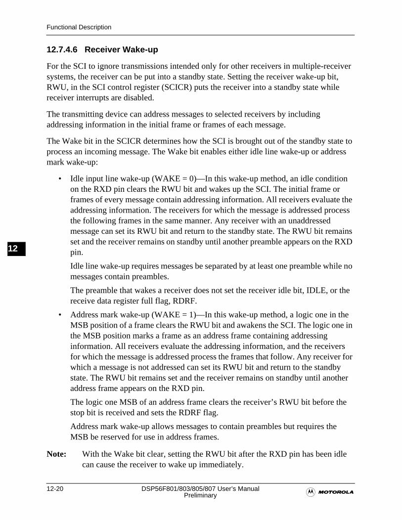
12-20 DSP56F801/803/805/807 User’s Manual�Preliminary
Functional Description
12
12.7.4.6 Receiver Wake-up
For the SCI to ignore transmissions intended only for other receivers in multiple-receiver systems, the receiver can be put into a standby state. Setting the receiver wake-up bit, RWU, in the SCI control register (SCICR) puts the receiver into a standby state while receiver interrupts are disabled.
The transmitting device can address messages to selected receivers by including addressing information in the initial frame or frames of each message.
The Wake bit in the SCICR determines how the SCI is brought out of the standby state to process an incoming message. The Wake bit enables either idle line wake-up or address mark wake-up:
• Idle input line wake-up (WAKE = 0)—In this wake-up method, an idle condition on the RXD pin clears the RWU bit and wakes up the SCI. The initial frame or frames of every message contain addressing information. All receivers evaluate the addressing information. The receivers for which the message is addressed process the following frames in the same manner. Any receiver with an unaddressed message can set its RWU bit and return to the standby state. The RWU bit remains set and the receiver remains on standby until another preamble appears on the RXD pin.
Idle line wake-up requires messages be separated by at least one preamble while no messages contain preambles.
The preamble that wakes a receiver does not set the receiver idle bit, IDLE, or the receive data register full flag, RDRF.
• Address mark wake-up (WAKE = 1)—In this wake-up method, a logic one in the MSB position of a frame clears the RWU bit and awakens the SCI. The logic one in the MSB position marks a frame as an address frame containing addressing information. All receivers evaluate the addressing information, and the receivers for which the message is addressed process the frames that follow. Any receiver for which a message is not addressed can set its RWU bit and return to the standby state. The RWU bit remains set and the receiver remains on standby until another address frame appears on the RXD pin.
The logic one MSB of an address frame clears the receiver’s RWU bit before the stop bit is received and sets the RDRF flag.
Address mark wake-up allows messages to contain preambles but requires the MSB be reserved for use in address frames.
Note: With the Wake bit clear, setting the RWU bit after the RXD pin has been idle can cause the receiver to wake up immediately.

Functional Description
�Serial Communications Interface Module (SCI) 12-21
Preliminary
12
12.7.5 Single-Wire Operation
Normally, the SCI uses two pins for transmitting and receiving. In single-wire operation, the RXD pin is disconnected from the SCI and is available as a GPIO pin. The SCI uses the TXD pin for both receiving and transmitting.
Setting the TE bit in the SCI control register (SCICR) configures TXD as the output for transmitted data. Clearing the TE bit configures TXD as the input for received data.
Figure 12-14. Single-Wire Operation (LOOPS = 1, RSRC = 1)
Enable single-wire operation by setting the Loops bit and the receiver source bit, RSRC, in the SCI control register (SCICR). Setting the Loops bit disables the path from the RXD pin to the receiver. Setting the RSRC bit connects the receiver input to the output of the TXD pin driver.
12.7.6 Loop Operation
In Loop operation the transmitter output goes to the receiver input. The RXD pin is disconnected from the SCI and is available as a general purpose I/O pin.
Setting the TE bit in the SCICR connects the transmitter output to the TXD pin. Clearing the TE bit disconnects the transmitter output from the TXD pin.
Figure 12-15. Loop Operation (LOOPS = 1, RSRC = 0)
Enable Loop operation by setting the Loops bit and clearing the RSRC bit in the SCICR. Setting the Loops bit disables the path from the RXD pin to the receiver. Clearing the RSRC bit connects the transmitter output to the receiver input. Both the transmitter and receiver must be enabled (TE = 1 and RE = 1).
TXD
RXD
TRANSMITTER
RECEIVER
TEGENERALPURPOSE I/O
TXD
RXD
TEGENERALPURPOSE I/O
TRANSMITTER
RECEIVER
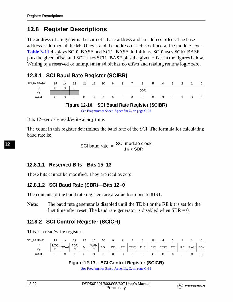
12-22 DSP56F801/803/805/807 User’s Manual�Preliminary
Register Descriptions
12
12.8 Register Descriptions
The address of a register is the sum of a base address and an address offset. The base address is defined at the MCU level and the address offset is defined at the module level. Table 3-11 displays SCI0_BASE and SCI1_BASE definitions. SCI0 uses SCI0_BASE plus the given offset and SCI1 uses SCI1_BASE plus the given offset in the figures below. Writing to a reserved or unimplemented bit has no effect and reading returns logic zero.
12.8.1 SCI Baud Rate Register (SCIBR)
Bits 12–zero are read/write at any time.
The count in this register determines the baud rate of the SCI. The formula for calculating baud rate is:
12.8.1.1 Reserved Bits—Bits 15–13
These bits cannot be modified. They are read as zero.
12.8.1.2 SCI Baud Rate (SBR)—Bits 12–0
The contents of the baud rate registers are a value from one to 8191.
Note: The baud rate generator is disabled until the TE bit or the RE bit is set for the first time after reset. The baud rate generator is disabled when SBR = 0.
12.8.2 SCI Control Register (SCICR)
This is a read/write register..
Figure 12-17. SCI Control Register (SCICR)See Programmer Sheet, Appendix C, on page C-99
SCI_BASE+$0 15 14 13 12 11 10 9 8 7 6 5 4 3 2 1 0
R 0 0 0SBR
W
reset 0 0 0 0 0 0 0 0 0 0 0 0 0 1 0 0
Figure 12-16. SCI Baud Rate Register (SCIBR)See Programmer Sheet, Appendix C, on page C-98
SCI_BASE+$1 15 14 13 12 11 10 9 8 7 6 5 4 3 2 1 0
R LOOP
SWAIRSR
CM
WAKE
POL PE PT TEIE TIIE RIE REIE TE RE RWU SBKW
reset 0 0 0 0 0 0 0 0 0 0 0 0 0 0 0 0
SCI baud rate SCI module clock16 SBR×
----------------------------------------------=
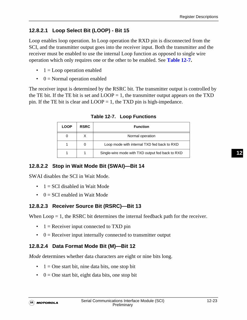
Register Descriptions
�Serial Communications Interface Module (SCI) 12-23
Preliminary
12
12.8.2.1 Loop Select Bit (LOOP) - Bit 15
Loop enables loop operation. In Loop operation the RXD pin is disconnected from the SCI, and the transmitter output goes into the receiver input. Both the transmitter and the receiver must be enabled to use the internal Loop function as opposed to single wire operation which only requires one or the other to be enabled. See Table 12-7.
• 1 = Loop operation enabled
• 0 = Normal operation enabled
The receiver input is determined by the RSRC bit. The transmitter output is controlled by the TE bit. If the TE bit is set and LOOP = 1, the transmitter output appears on the TXD pin. If the TE bit is clear and LOOP = 1, the TXD pin is high-impedance.
12.8.2.2 Stop in Wait Mode Bit (SWAI)—Bit 14
SWAI disables the SCI in Wait Mode.
• 1 = SCI disabled in Wait Mode
• 0 = SCI enabled in Wait Mode
12.8.2.3 Receiver Source Bit (RSRC)—Bit 13
When Loop = 1, the RSRC bit determines the internal feedback path for the receiver.
• 1 = Receiver input connected to TXD pin
• 0 = Receiver input internally connected to transmitter output
12.8.2.4 Data Format Mode Bit (M)—Bit 12
Mode determines whether data characters are eight or nine bits long.
• 1 = One start bit, nine data bits, one stop bit
• 0 = One start bit, eight data bits, one stop bit
Table 12-7. Loop Functions
LOOP RSRC Function
0 X Normal operation
1 0 Loop mode with internal TXD fed back to RXD
1 1 Single-wire mode with TXD output fed back to RXD
12-24 DSP56F801/803/805/807 User’s Manual�Preliminary
Register Descriptions
12
12.8.2.5 Wake-up Condition Bit (WAKE)—Bit 11
Wake determines which condition wakes up the SCI: a logic one, address mark, in the most significant bit position of a received data character or an idle condition on the RXD pin.
• 1 = Address mark wake-up
• 0 = Idle line wake-up
12.8.2.6 Polarity Bit (POL)—Bit 10
POL determines whether or not to invert the data as it goes from the transmitter to the TXD pin and from the RXD pin to the receiver. All bits, start, data, and stop will be inverted as they leave the transmit shift register and before they enter the receive shift register.
• 1 = Invert transmit and receive data bits (Inverted Mode)
• 0 = Do not invert transmit and receive data bits (Normal Mode)
Note: Recommended: the POL bit be toggled only when TE = 0 and RE = 0.
12.8.2.7 Parity Enable Bit (PE)—Bit 9
PE enables the parity function. When enabled, the parity function replaces the most significant bit of the data character with a parity bit.
• 1 = Parity function enabled
• 0 = Parity function disabled
12.8.2.8 Parity Type Bit (PT)—Bit 8
PT determines whether the SCI generates and checks for even parity or odd parity of the data bits. With even parity, an even number of ones clears the parity bit and an odd number of ones sets the parity bit. With odd parity, an odd number of ones clears the parity bit and an even number of ones sets the parity bit.
• 1 = Odd parity
• 0 = Even parity
12.8.2.9 Transmitter Empty Interrupt Enable Bit (TEIE)—Bit 7
TEIE enables the transmit data register empty flag, TDRE, to generate interrupt requests.
• 1 = TDRE interrupt requests enabled
Register Descriptions
�Serial Communications Interface Module (SCI) 12-25
Preliminary
12
• 0 = TDRE interrupt requests disabled
12.8.2.10 Transmitter Idle Interrupt Enable Bit (TIIE)—Bit 6
TIIE enables the transmitter idle flag, TI, to generate interrupt requests.
• 1 = TI interrupt requests enabled
• 0 = TI interrupt requests disabled
12.8.2.11 Receiver Full Interrupt Enable Bit (RIE)—Bit 5
RIE enables the receive data register full flag, RDRF, the overrun flag, OR. It will also generate interrupt requests.
• 1 = RDRF and OR interrupt requests enabled
• 0 = RDRF and OR interrupt requests disabled
12.8.2.12 Receive Error Interrupt Enable Bit (REIE)—Bit 4
REIE enables the receive error flags, NF, PF, FE, and OR to generate interrupt requests.
• 1 = Error interrupt requests enabled
• 0 = Error interrupt requests disabled
12.8.2.13 Transmitter Enable Bit (TE)—Bit 3
TE enables the SCI transmitter and configures the TXD pin as the SCI transmitter output. The TE bit can be used to queue an idle preamble.
• 1 = Transmitter enabled
• 0 = Transmitter disabled - TXD pin is in high impedance state.
12.8.2.14 Receiver Enable Bit (RE)—Bit 2
RE enables the SCI receiver.
• 1 = Receiver enabled
• 0 = Receiver disabled
12.8.2.15 Receiver Wake-up Bit (RWU)—Bit 1
RWU enables the wake-up function and inhibits further receiver interrupt requests. Normally, hardware awakens the receiver by automatically clearing RWU.
• 1 = Standby state
• 0 = Normal operation
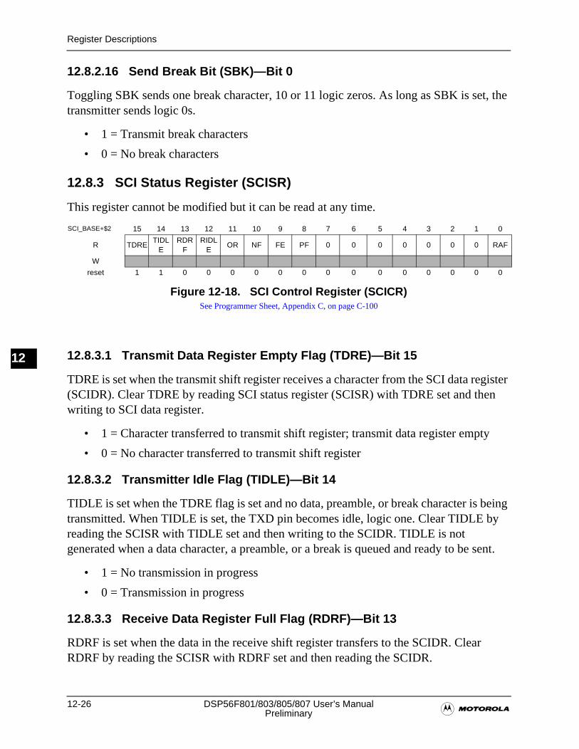
12-26 DSP56F801/803/805/807 User’s Manual�Preliminary
Register Descriptions
12
12.8.2.16 Send Break Bit (SBK)—Bit 0
Toggling SBK sends one break character, 10 or 11 logic zeros. As long as SBK is set, the transmitter sends logic 0s.
• 1 = Transmit break characters
• 0 = No break characters
12.8.3 SCI Status Register (SCISR)
This register cannot be modified but it can be read at any time.
12.8.3.1 Transmit Data Register Empty Flag (TDRE)—Bit 15
TDRE is set when the transmit shift register receives a character from the SCI data register (SCIDR). Clear TDRE by reading SCI status register (SCISR) with TDRE set and then writing to SCI data register.
• 1 = Character transferred to transmit shift register; transmit data register empty
• 0 = No character transferred to transmit shift register
12.8.3.2 Transmitter Idle Flag (TIDLE)—Bit 14
TIDLE is set when the TDRE flag is set and no data, preamble, or break character is being transmitted. When TIDLE is set, the TXD pin becomes idle, logic one. Clear TIDLE by reading the SCISR with TIDLE set and then writing to the SCIDR. TIDLE is not generated when a data character, a preamble, or a break is queued and ready to be sent.
• 1 = No transmission in progress
• 0 = Transmission in progress
12.8.3.3 Receive Data Register Full Flag (RDRF)—Bit 13
RDRF is set when the data in the receive shift register transfers to the SCIDR. Clear RDRF by reading the SCISR with RDRF set and then reading the SCIDR.
SCI_BASE+$2 15 14 13 12 11 10 9 8 7 6 5 4 3 2 1 0
R TDRETIDL
ERDR
FRIDL
EOR NF FE PF 0 0 0 0 0 0 0 RAF
W
reset 1 1 0 0 0 0 0 0 0 0 0 0 0 0 0 0
Figure 12-18. SCI Control Register (SCICR)See Programmer Sheet, Appendix C, on page C-100
Register Descriptions
�Serial Communications Interface Module (SCI) 12-27
Preliminary
12
• 1 = Received data available in SCI data register
• 0 = Data not available in SCI data register
12.8.3.4 Receiver Idle Line Flag (RIDLE)—Bit 12
RIDLE is set when 10 consecutive logic ones, if M = 0, or 11 consecutive logic ones, if M = 1 appear on the receiver input. Once the RIDLE flag is cleared the receiver detects a logic zero, then a valid frame must again set the RDRF flag before an idle condition can set the RIDLE flag.
• 1 = Receiver input has become idle, after receiving a valid frame
• 0 = Receiver input is either active now or has never become active since the RIDLE flag was last cleared
Note: When the receiver wake-up bit, RWU in the SCICR is set, an idle line condition does not set the RIDLE flag.
12.8.3.5 Overrun Flag (OR)—Bit 11
OR is set when software fails to read the SCIDR before the receive shift register receives the next frame. The data in the shift register is lost, but the data already in the SCIDR is not affected. Clear OR by reading the SCISR with OR set and then writing the SCISR with any value.
• 1 = Overrun
• 0 = No overrun
12.8.3.6 Noise Flag (NF)—Bit 10
NF is set when the SCI detects noise on the receiver input. NF bit is set during the same cycle as the RDRF flag but does not get set in the case of an overrun. Clear NF by reading the SCISR and then writing the SCISR with any value.
• 1 = Noise
• 0 = No noise
12.8.3.7 Framing Error Flag (FE)—Bit 9
FE is set when a logic zero is accepted as the stop bit. FE bit is set during the same cycle as the RDRF flag, but does not get set in the case of an overrun. FE inhibits further data reception until it is cleared. Clear FE by reading the SCISR with FE set and then writing the SCISR with any value.
• 1 = Framing error
• 0 = No framing error
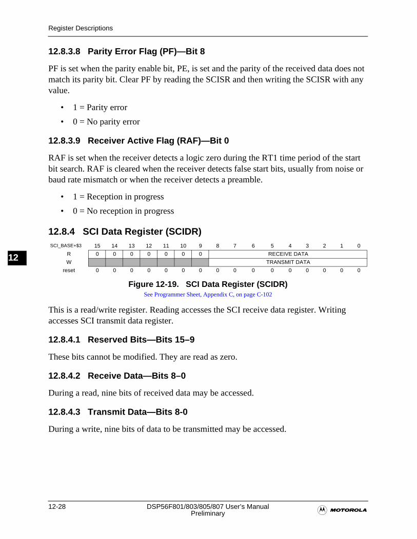
12-28 DSP56F801/803/805/807 User’s Manual�Preliminary
Register Descriptions
12
12.8.3.8 Parity Error Flag (PF)—Bit 8
PF is set when the parity enable bit, PE, is set and the parity of the received data does not match its parity bit. Clear PF by reading the SCISR and then writing the SCISR with any value.
• 1 = Parity error
• 0 = No parity error
12.8.3.9 Receiver Active Flag (RAF)—Bit 0
RAF is set when the receiver detects a logic zero during the RT1 time period of the start bit search. RAF is cleared when the receiver detects false start bits, usually from noise or baud rate mismatch or when the receiver detects a preamble.
• 1 = Reception in progress
• 0 = No reception in progress
12.8.4 SCI Data Register (SCIDR)
This is a read/write register. Reading accesses the SCI receive data register. Writing accesses SCI transmit data register.
12.8.4.1 Reserved Bits—Bits 15–9
These bits cannot be modified. They are read as zero.
12.8.4.2 Receive Data—Bits 8–0
During a read, nine bits of received data may be accessed.
12.8.4.3 Transmit Data—Bits 8-0
During a write, nine bits of data to be transmitted may be accessed.
SCI_BASE+$3 15 14 13 12 11 10 9 8 7 6 5 4 3 2 1 0
R 0 0 0 0 0 0 0 RECEIVE DATA
W TRANSMIT DATA
reset 0 0 0 0 0 0 0 0 0 0 0 0 0 0 0 0
Figure 12-19. SCI Data Register (SCIDR)See Programmer Sheet, Appendix C, on page C-102
Low-Power Options
�Serial Communications Interface Module (SCI) 12-29
Preliminary
12
12.9 Low-Power Options
12.9.1 Run Mode
Clearing the transmitter enable or receiver enable bits, TE or RE, in the SCICR reduces power consumption in run mode. SCI registers are still accessible when TE or RE is cleared, but clocks to the core of the SCI are disabled.
12.9.2 Wait Mode
SCI operation in Wait Mode depends on the state of the SWAI bit in the SCICR.
• If SWAI is zero, the SCI operates normally when the CPU is in Wait Mode
• If SWAI is one, SCI clock generation ceases and the SCI module enters a power-conservation state when the CPU is in Wait Mode. In this condition, SCI registers are not accessible. Setting SWAI does not affect the state of the receiver enable bit, RE, or the transmitter enable bit, TE
If SWAI is one, any transmission or reception in progress stops at Wait Mode entry. The transmission or reception resumes when either an internal or external interrupt brings the MCU out of Wait Mode. Exiting Wait Mode by reset aborts any transmission or reception in progress and resets the SCI
12.9.3 Stop Mode
The SCI is inactive in Stop Mode for reduced power consumption. The stop instruction does not affect SCI register states. SCI operation resumes after an external interrupt brings the CPU out of Stop Mode. Exiting Stop Mode by reset aborts any transmission or reception in progress and resets the SCI.
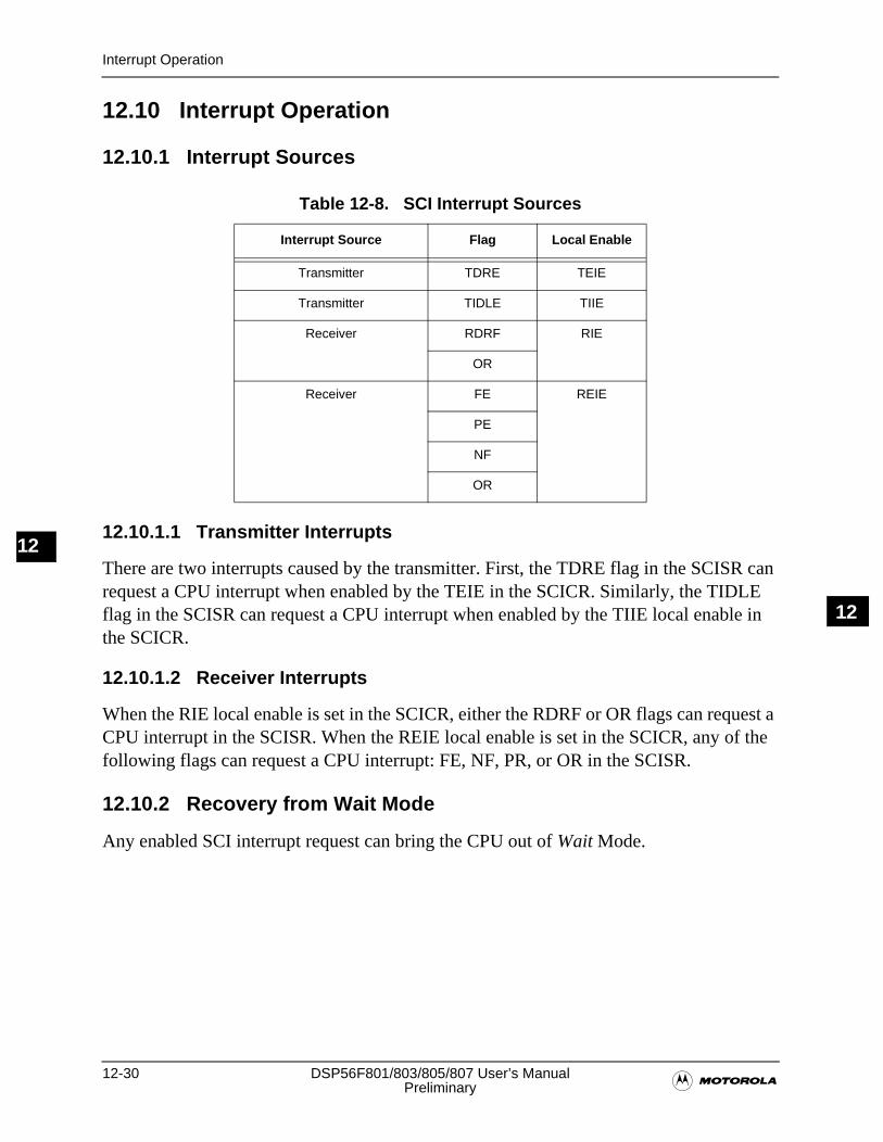
12-30 DSP56F801/803/805/807 User’s Manual�Preliminary
Interrupt Operation
12
12.10 Interrupt Operation
12.10.1 Interrupt Sources
12.10.1.1 Transmitter Interrupts
There are two interrupts caused by the transmitter. First, the TDRE flag in the SCISR can request a CPU interrupt when enabled by the TEIE in the SCICR. Similarly, the TIDLE flag in the SCISR can request a CPU interrupt when enabled by the TIIE local enable in the SCICR.
12.10.1.2 Receiver Interrupts
When the RIE local enable is set in the SCICR, either the RDRF or OR flags can request a CPU interrupt in the SCISR. When the REIE local enable is set in the SCICR, any of the following flags can request a CPU interrupt: FE, NF, PR, or OR in the SCISR.
12.10.2 Recovery from Wait Mode
Any enabled SCI interrupt request can bring the CPU out of Wait Mode.
Table 12-8. SCI Interrupt Sources
Interrupt Source Flag Local Enable
Transmitter TDRE TEIE
Transmitter TIDLE TIIE
Receiver RDRF RIE
OR
Receiver FE REIE
PE
NF
OR
12
�Serial Peripheral Interface (SPI) 13-1
Preliminary
13
Chapter 13Serial Peripheral Interface (SPI)

13-2 DSP56F801/803/805/807 User’s Manual�Preliminary
13
Features
�Serial Peripheral Interface (SPI) 13-3
Preliminary
13
13.1 Introduction
This section describes the Serial Peripheral Interface Module (SPI). The SPI module allows full-duplex, synchronous, serial communication between the DSP and peripheral devices, including other DPSs. Software can poll the SPI status flags or SPI operation can be interrupt driven. This block contains four, 16-bit memory mapped registers for control parameters, status, and data transfer. The DSP56F801/803/805/807 has one SPI with four pins able to alternately be used as GPIO pins if the SPI is not required.
13.2 Features
Features of the SPI module include the following:
• Full-Duplex Operation
• Master and Slave Modes
• Double-Buffered Operation With Separate Transmit and Receive Registers
• Programmable Length Transmissions, 2 to 16 Bits
• Programmable Transmit and Receive Shift Order, MSB First or Last Bit Transmitted
• Four Master Mode Frequencies (Maximum = Bus Frequency ÷ 2)
• Maximum Slave Mode Frequency = Bus Frequency
• Clock Ground for Reduced Radio Frequency (RF) Interference
• Serial Clock with Programmable Polarity and Phase
• Two Separately Enabled Interrupts:
— SPRF (SPI Receiver Full)
— SPTE (SPI Transmitter Empty)
• Mode Fault Error Flag With DSP Interrupt Capability
• Overflow Error Flag with DSP Interrupt Capability
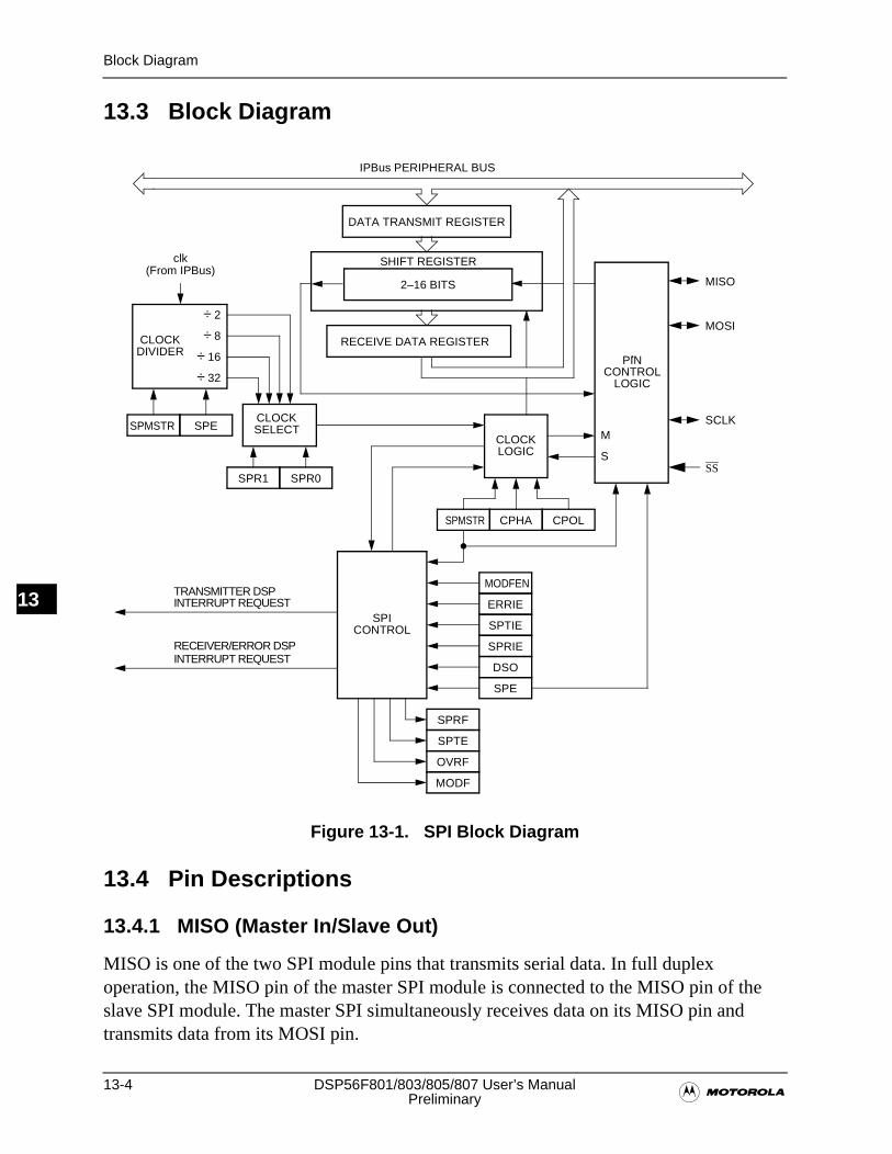
13-4 DSP56F801/803/805/807 User’s Manual�Preliminary
Block Diagram
13
13.3 Block Diagram
Figure 13-1. SPI Block Diagram
13.4 Pin Descriptions
13.4.1 MISO (Master In/Slave Out)
MISO is one of the two SPI module pins that transmits serial data. In full duplex operation, the MISO pin of the master SPI module is connected to the MISO pin of the slave SPI module. The master SPI simultaneously receives data on its MISO pin and transmits data from its MOSI pin.
TRANSMITTER DSP
RECEIVER/ERROR DSP
SPR1
SPMSTR
DATA TRANSMIT REGISTER
SHIFT REGISTER
SPR0
clk
CLOCKSELECT
÷ 2
CLOCKDIVIDER
÷ 8
÷ 16
÷ 32
CLOCKLOGIC
CPHA CPOL
SPI
SPRIE
DSO
SPE
SPRF
SPTE
OVRF
M
S
PINCONTROL
LOGIC
RECEIVE DATA REGISTER
SPTIE
SPE
IPBus PERIPHERAL BUS
(From IPBus)
MODFEN
ERRIE
CONTROL
MODF
SPMSTR
MOSI
MISO
SCLK
SS
2–16 BITS
INTERRUPT REQUEST
INTERRUPT REQUEST
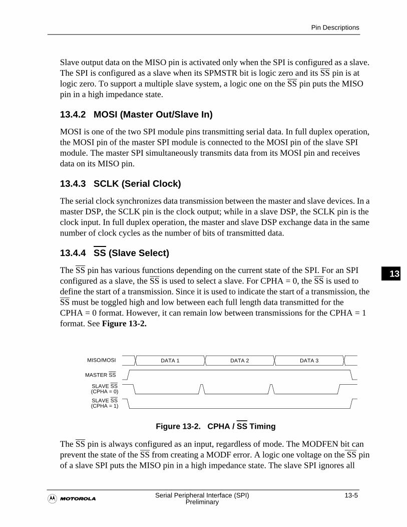
Pin Descriptions
�Serial Peripheral Interface (SPI) 13-5
Preliminary
13
Slave output data on the MISO pin is activated only when the SPI is configured as a slave. The SPI is configured as a slave when its SPMSTR bit is logic zero and its SS pin is at logic zero. To support a multiple slave system, a logic one on the SS pin puts the MISO pin in a high impedance state.
13.4.2 MOSI (Master Out/Slave In)
MOSI is one of the two SPI module pins transmitting serial data. In full duplex operation, the MOSI pin of the master SPI module is connected to the MOSI pin of the slave SPI module. The master SPI simultaneously transmits data from its MOSI pin and receives data on its MISO pin.
13.4.3 SCLK (Serial Clock)
The serial clock synchronizes data transmission between the master and slave devices. In a master DSP, the SCLK pin is the clock output; while in a slave DSP, the SCLK pin is the clock input. In full duplex operation, the master and slave DSP exchange data in the same number of clock cycles as the number of bits of transmitted data.
13.4.4 SS (Slave Select)
The SS pin has various functions depending on the current state of the SPI. For an SPI configured as a slave, the SS is used to select a slave. For CPHA = 0, the SS is used to define the start of a transmission. Since it is used to indicate the start of a transmission, the SS must be toggled high and low between each full length data transmitted for the CPHA = 0 format. However, it can remain low between transmissions for the CPHA = 1 format. See Figure 13-2.
Figure 13-2. CPHA / SS Timing
The SS pin is always configured as an input, regardless of mode. The MODFEN bit can prevent the state of the SS from creating a MODF error. A logic one voltage on the SS pin of a slave SPI puts the MISO pin in a high impedance state. The slave SPI ignores all
DATA 1 DATA 3MISO/MOSI DATA 2
MASTER SS
SLAVE SS(CPHA = 0)
SLAVE SS(CPHA = 1)
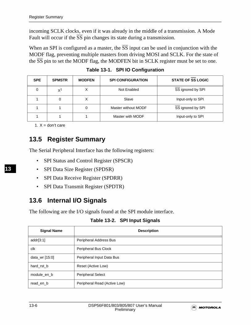
13-6 DSP56F801/803/805/807 User’s Manual�Preliminary
Register Summary
13
incoming SCLK clocks, even if it was already in the middle of a transmission. A Mode Fault will occur if the SS pin changes its state during a transmission.
When an SPI is configured as a master, the SS input can be used in conjunction with the MODF flag, preventing multiple masters from driving MOSI and SCLK. For the state of the SS pin to set the MODF flag, the MODFEN bit in SCLK register must be set to one.
13.5 Register Summary
The Serial Peripheral Interface has the following registers:
• SPI Status and Control Register (SPSCR)
• SPI Data Size Register (SPDSR)
• SPI Data Receive Register (SPDRR)
• SPI Data Transmit Register (SPDTR)
13.6 Internal I/O Signals
The following are the I/O signals found at the SPI module interface.
Table 13-1. SPI IO Configuration
SPE SPMSTR MODFEN SPI CONFIGURATION STATE OF SS LOGIC
0 X1
1. X = don’t care
X Not Enabled SS ignored by SPI
1 0 X Slave Input-only to SPI
1 1 0 Master without MODF SS ignored by SPI
1 1 1 Master with MODF Input-only to SPI
Table 13-2. SPI Input Signals
Signal Name Description
addr[3:1] Peripheral Address Bus
clk Peripheral Bus Clock
data_wr [15:0] Peripheral Input Data Bus
hard_rst_b Reset (Active Low)
module_en_b Peripheral Select
read_en_b Peripheral Read (Active Low)
External I/O Signals
�Serial Peripheral Interface (SPI) 13-7
Preliminary
13
13.7 External I/O Signals
The following are external I/O signals for the chip interface.
write_en_b Peripheral Write (Active Low)
spimiso_in Master-in Slave-out input signal for pad pin MISO
spimosi_in Master-out Slave-in input signal for pad pin MOSI
spisck_in Slave clock input for pad pin SCLK
spiss_b Slave select (Active Low) for pad pin SS
Table 13-3. SPI Output Signals
Signal Name Description
data_rd [15:0] Peripheral Output Data Bus
sprferrireq_b Active low when SPI issuing a receiver full or error DSP interrupt (see interrupts)
spteireq_b Active low when SPI issuing a transmitter empty DSP interrupt (see interrupts)
spimiso_out Master-in Slave-out output signal for pad pin MISO
spimosi_out Master-out Slave-in output signal for pad pin MOSI
spisck_out Slave clock output for pad pin SCLK
enable_mosi_b Directional enable for MOSI
enable_sclk_b Directional enable for SCLK pads
enable_miso_b Directional enable for MISO pad
Table 13-4. External I/O Signals
Signal Name Description Direction
MOSI Master-out Slave-in Pad Pin Bi-Directional
MISO Master-in Slave-out Pad Pin Bi-Directional
SCLK Slave Clock Pad Pin Bi-Directional
SS Slave Select Pad Pin (Active Low) Input
Table 13-2. SPI Input Signals (Continued)
Signal Name Description
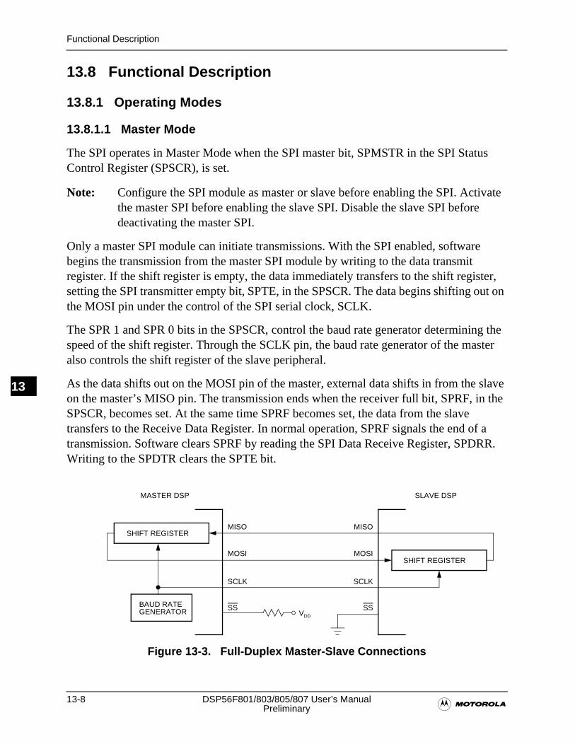
13-8 DSP56F801/803/805/807 User’s Manual�Preliminary
Functional Description
13
13.8 Functional Description
13.8.1 Operating Modes
13.8.1.1 Master Mode
The SPI operates in Master Mode when the SPI master bit, SPMSTR in the SPI Status Control Register (SPSCR), is set.
Note: Configure the SPI module as master or slave before enabling the SPI. Activate the master SPI before enabling the slave SPI. Disable the slave SPI before deactivating the master SPI.
Only a master SPI module can initiate transmissions. With the SPI enabled, software begins the transmission from the master SPI module by writing to the data transmit register. If the shift register is empty, the data immediately transfers to the shift register, setting the SPI transmitter empty bit, SPTE, in the SPSCR. The data begins shifting out on the MOSI pin under the control of the SPI serial clock, SCLK.
The SPR 1 and SPR 0 bits in the SPSCR, control the baud rate generator determining the speed of the shift register. Through the SCLK pin, the baud rate generator of the master also controls the shift register of the slave peripheral.
As the data shifts out on the MOSI pin of the master, external data shifts in from the slave on the master’s MISO pin. The transmission ends when the receiver full bit, SPRF, in the SPSCR, becomes set. At the same time SPRF becomes set, the data from the slave transfers to the Receive Data Register. In normal operation, SPRF signals the end of a transmission. Software clears SPRF by reading the SPI Data Receive Register, SPDRR. Writing to the SPDTR clears the SPTE bit.
Figure 13-3. Full-Duplex Master-Slave Connections
SHIFT REGISTER
SHIFT REGISTER
BAUD RATEGENERATOR
MASTER DSP SLAVE DSP
VDD
MOSI MOSI
MISO MISO
SCLK SCLK
SS SS
Functional Description
�Serial Peripheral Interface (SPI) 13-9
Preliminary
13
13.8.1.2 Slave Mode
The SPI operates in Slave Mode when the SPMSTR bit in the SPI Status Control Register (SPSCR) is clear. In Slave Mode, the SCLK pin is the input for the serial clock from the master DSP. Before a data transmission occurs, the SS pin of the slave SPI must be at logic zero. SS must remain low until the transmission is complete or a Mode Fault error will occur.
Note: The SPI must be activated (SPE = 1 in the SPI Status Control Register (SPSCR)) to receive slave transmissions.
In a slave SPI module, data enters the shift register under the control of the serial clock, SCLK, from the master SPI module. After a full length data transmission enters the shift register of a slave SPI, it transfers to the Receive Data Register (SPDRR) and the SPRF bit in the SPSCR is set. To prevent an overflow condition, slave software then must read the SPDRR before another full length data transmission enters the shift register.
The maximum frequency of the SCLK for an SPI configured as a slave is the bus clock speed. This is twice as fast as the fastest master SCLK clock can be generated. The frequency of the SCLK for an SPI configured as a slave does not have to correspond to any SPI baud rate. The baud rate only controls the speed of the SCLK generated by an SPI configured as a master. Therefore, the frequency of the SCLK for an SPI configured as a slave can be any frequency less than or equal to the bus speed.
When the master SPI starts a transmission, the data in the slave shift register begins shifting out on the MISO pin. The slave can load its shift register with new data for the next transmission by writing to its data transmit register. The slave must write to its data transmit register at least one bus cycle before the master starts the next transmission. Otherwise, the data already in the slave shift register shifts out on the MISO pin. Data written to the slave shift register during a transmission remains in a buffer until the end of the transmission.
When the clock phase bit, CPHA in the SPI Status Control Register (SPSCR) is set, the first edge of SCLK starts a transmission. When CPHA is clear, the falling edge of SS starts a transmission.
Note: SCLK must be in the proper idle state before the slave is enabled to prevent SCLK from appearing as a clock edge.
13-10 DSP56F801/803/805/807 User’s Manual�Preliminary
Functional Description
13
13.8.2 Transmission Formats
During an SPI transmission, data is simultaneously transmitted, or shifted out serially, and received, shifted in serially. A serial clock synchronizes shifting and sampling on the two serial data lines. A slave select line allows selection of an individual slave SPI device; slave devices not selected do not interfere with SPI bus activities. On a master SPI device, the slave select line can be optionally used to indicate multiple-master bus contention.
13.8.2.1 Data Transmission Length
The SPI can support data lengths of two to 16 bits. This can be configured in the Data Size Register (SPDSR). When the data length is less than 16 bits, the Receive Data Register (SPDRR) will pad the upper bits with zeros. It is the responsibility of software to remove these upper bits, since 16 bits will be read simultaneously while reading the SPDRR.
Note: Data can be lost if the data length is not the same for both master and slave devices.
13.8.2.2 Data Shift Ordering
The SPI can be configured to transmit or receive the MSB of the desired data first or last. This is controlled by the Data Shift Order (DSO) bit in the SPSCR. Regardless which bit is transmitted or received first. Data shall always be written to the SPDTR and read from the SPDRR with the LSB in bit zero. The MSB will be in correct position depending on the data transmission size.
13.8.2.3 Clock Phase and Polarity Controls
Software can select any of four combinations of Serial Clock (SCLK) phase and polarity using two bits in the SPI Control Register (SPCR). The clock polarity is specified by the CPOL control bit, designed to select an active high or low clock. It has no significant effect on the transmission format.
The Clock Phase (CPHA) control bit selects one of two fundamentally different transmission formats. The clock phase and polarity should be identical for the master SPI device and the communicating slave device. In some cases, the phase and polarity are changed between transmissions allowing a master device to communicate with peripheral slaves with different requirements.
Note: Before writing to the CPOL bit or the CPHA bit, disable the SPI by clearing the SPI Enable bit (SPE). All these bits are in the SPSCR.
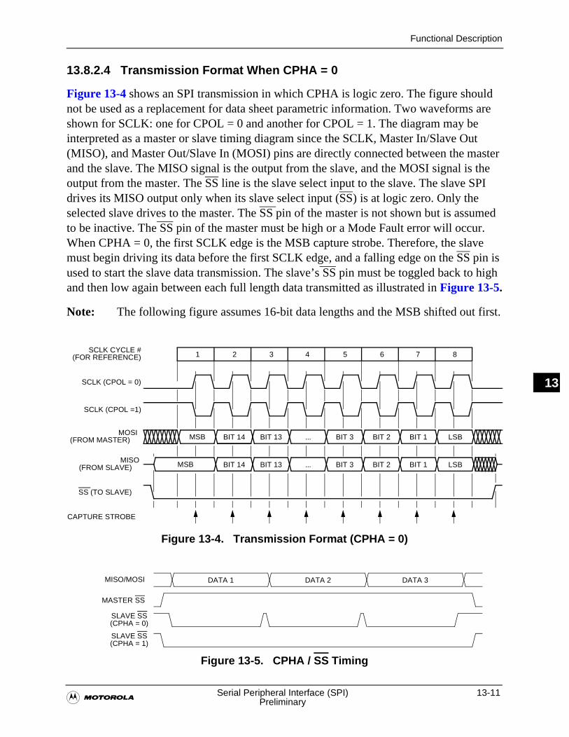
Functional Description
�Serial Peripheral Interface (SPI) 13-11
Preliminary
13
13.8.2.4 Transmission Format When CPHA = 0
Figure 13-4 shows an SPI transmission in which CPHA is logic zero. The figure should not be used as a replacement for data sheet parametric information. Two waveforms are shown for SCLK: one for CPOL = 0 and another for CPOL = 1. The diagram may be interpreted as a master or slave timing diagram since the SCLK, Master In/Slave Out (MISO), and Master Out/Slave In (MOSI) pins are directly connected between the master and the slave. The MISO signal is the output from the slave, and the MOSI signal is the output from the master. The SS line is the slave select input to the slave. The slave SPI drives its MISO output only when its slave select input (SS) is at logic zero. Only the selected slave drives to the master. The SS pin of the master is not shown but is assumed to be inactive. The SS pin of the master must be high or a Mode Fault error will occur. When CPHA = 0, the first SCLK edge is the MSB capture strobe. Therefore, the slave must begin driving its data before the first SCLK edge, and a falling edge on the SS pin is used to start the slave data transmission. The slave’s SS pin must be toggled back to high and then low again between each full length data transmitted as illustrated in Figure 13-5.
Note: The following figure assumes 16-bit data lengths and the MSB shifted out first.
Figure 13-4. Transmission Format (CPHA = 0)
Figure 13-5. CPHA / SS Timing
BIT 14 BIT 13 ... BIT 3 BIT 2 BIT 1 LSBMSB
BIT 14 BIT 13 ... BIT 3 BIT 2 BIT 1 LSBMSB
1 2 3 4 5 6 7 8SCLK CYCLE #
(FOR REFERENCE)
SCLK (CPOL = 0)
SCLK (CPOL =1)
MOSI(FROM MASTER)
MISO(FROM SLAVE)
SS (TO SLAVE)
CAPTURE STROBE
DATA 1 DATA 3MISO/MOSI DATA 2
MASTER SS
SLAVE SS(CPHA = 0)
SLAVE SS(CPHA = 1)
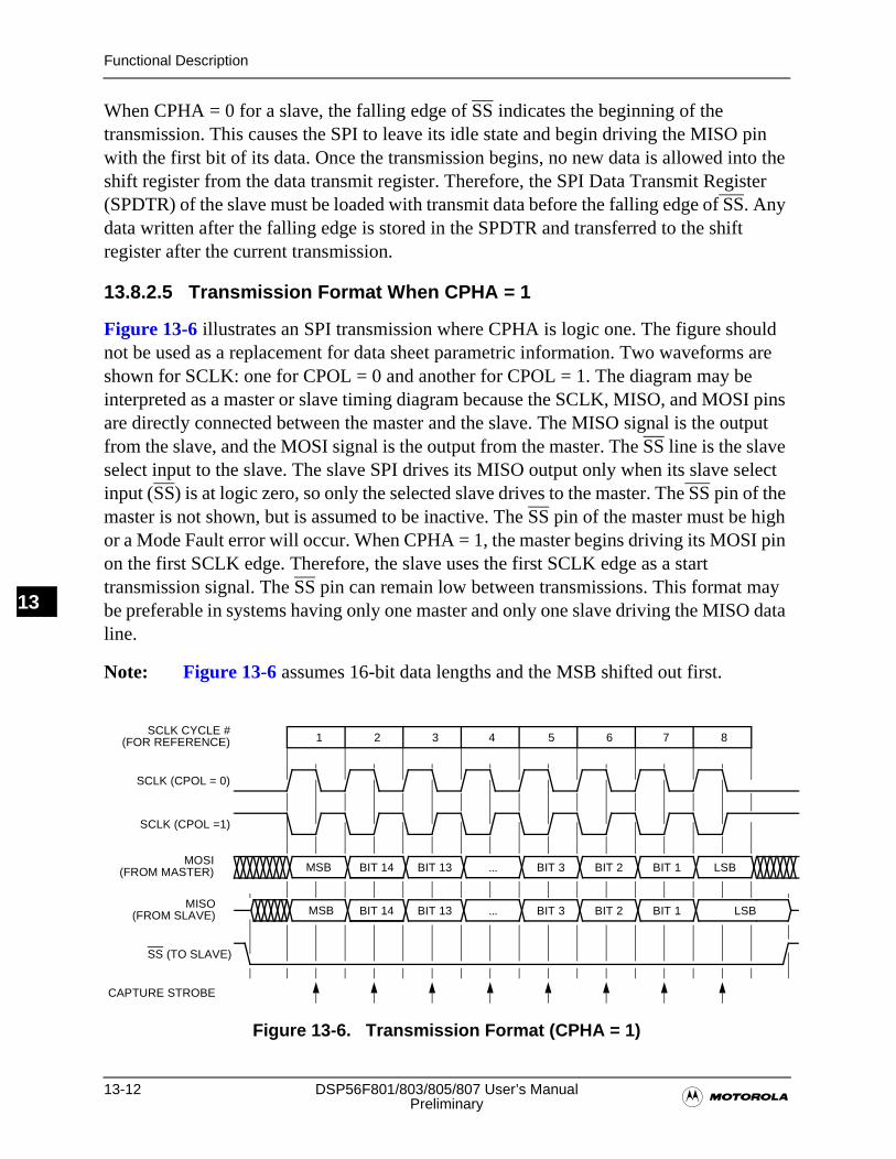
13-12 DSP56F801/803/805/807 User’s Manual�Preliminary
Functional Description
13
When CPHA = 0 for a slave, the falling edge of SS indicates the beginning of the transmission. This causes the SPI to leave its idle state and begin driving the MISO pin with the first bit of its data. Once the transmission begins, no new data is allowed into the shift register from the data transmit register. Therefore, the SPI Data Transmit Register (SPDTR) of the slave must be loaded with transmit data before the falling edge of SS. Any data written after the falling edge is stored in the SPDTR and transferred to the shift register after the current transmission.
13.8.2.5 Transmission Format When CPHA = 1
Figure 13-6 illustrates an SPI transmission where CPHA is logic one. The figure should not be used as a replacement for data sheet parametric information. Two waveforms are shown for SCLK: one for CPOL = 0 and another for CPOL = 1. The diagram may be interpreted as a master or slave timing diagram because the SCLK, MISO, and MOSI pins are directly connected between the master and the slave. The MISO signal is the output from the slave, and the MOSI signal is the output from the master. The SS line is the slave select input to the slave. The slave SPI drives its MISO output only when its slave select input (SS) is at logic zero, so only the selected slave drives to the master. The SS pin of the master is not shown, but is assumed to be inactive. The SS pin of the master must be high or a Mode Fault error will occur. When CPHA = 1, the master begins driving its MOSI pin on the first SCLK edge. Therefore, the slave uses the first SCLK edge as a start transmission signal. The SS pin can remain low between transmissions. This format may be preferable in systems having only one master and only one slave driving the MISO data line.
Note: Figure 13-6 assumes 16-bit data lengths and the MSB shifted out first.
Figure 13-6. Transmission Format (CPHA = 1)
BIT 14 BIT 13 ... BIT 3 BIT 2 BIT 1 LSBMSB
BIT 14 BIT 13 ... BIT 3 BIT 2 BIT 1 LSBMSB
1 2 3 4 5 6 7 8SCLK CYCLE #
(FOR REFERENCE)
SCLK (CPOL = 0)
SCLK (CPOL =1)
MOSI(FROM MASTER)
MISO(FROM SLAVE)
SS (TO SLAVE)
CAPTURE STROBE
Functional Description
�Serial Peripheral Interface (SPI) 13-13
Preliminary
13
When CPHA = 1 for a slave, the first edge of the SCLK indicates the beginning of the transmission. This causes the SPI to leave its idle state and begin driving the MISO pin with the first bit of its data. Once the transmission begins, no new data is allowed into the shift register from the data transmit register. Therefore, the SPI data register of the slave must be loaded with transmit data before the first edge of SCLK. Any data written after the first edge is stored in the data transmit register and transferred to the shift register after the current transmission.
13.8.2.6 Transmission Initiation Latency
When the SPI is configured as a master (SPMSTR = 1 in the SPSCR), writing to the SPI Data Transmit Register (SPDTR) starts a transmission. CPHA has no effect on the delay to the start of the transmission. However, it does affect the initial state of the SCLK signal:
• When CPHA = 0, the SCLK signal remains inactive for the first half of the first SCLK cycle
• When CPHA = 1, the first SCLK cycle begins with an edge on the SCLK line from its inactive to its active level
• The SPI clock rate, selected by SPR1:SPR0, affects the delay from the write to SPDTR and the start of the SPI transmission
The internal SPI clock in the master is a free-running derivative of the internal DSP clock. To conserve power, it is activated only when both the SPE and SPMSTR bits are set. Because the SPI clock is free-running, it is uncertain where the write to the SPDTR occurs relative to the slower SCLK. This uncertainty causes the variation in the initiation delay illustrated in Figure 13-7. This delay is no longer than a single SPI bit time. That is, the maximum delay is 2-DSP bus cycles for DIV2, 8-DSP bus cycles for DIV8, 16-DSP bus cycles for DIV16, and 32-DSP bus cycles for DIV32.
Note: Figure 13-7 assumes 16-bit data lengths and the MSB shifted out first.
13.8.3 Transmission Data
The double-buffered data transmit register allows data to be queued and transmitted. For an SPI configured as a master, the queued data is transmitted immediately after the previous transmission has completed. The SPI Transmitter Empty flag (SPTE) indicates when the data transmit buffer is ready to accept new data. Write to the SPI Data Transmit Register (SPDTR) only when the SPTE bit is high. Figure 13-8 illustrates the timing associated with doing back-to-back transmissions with the SPI, SCLK has CPHA: CPOL equals 1:0.
Note: Figure 13-8 assumes 16-bit data lengths and the MSB shifted out first.
13-14 DSP56F801/803/805/807 User’s Manual�Preliminary
Functional Description
13
The data transmit buffer allows back-to-back transmissions without the slave precisely timing its writes between transmissions, as in a system with a single data buffer. Also, if no new data is written to the data buffer, the last value contained in the shift register is the next data to be transmitted.
For an idle master or idle slave not being data loaded into its transmit buffer, the SPTE is set again no more than two bus cycles after the transmit buffer empties into the shift register. This allows the user to queue up at most a 32-bit value to send. For an already active slave, the load of the shift register cannot occur until the transmission is completed. This implies a back-to-back write to the data transmit register is not possible. The SPI Transmitter Empty Bit (SPTE) in the SPSCR indicates when the next write can occur.
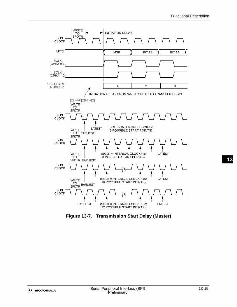
Functional Description
�Serial Peripheral Interface (SPI) 13-15
Preliminary
13
Figure 13-7. Transmission Start Delay (Master)
WRITETO INITIATION DELAY
BUS
MOSI
SCLK(CPHA = 1)
SCLK(CPHA = 0)
SCLK CYCLENUMBER
MSB BIT 15
1 2
CLOCK
WRITETO
EARLIEST
LATEST (SCLK = INTERNAL CLOCK ³ 2;
EARLIEST
LATEST
2 POSSIBLE START POINTS)
(SCLK = INTERNAL CLOCK ³ 8;8 POSSIBLE START POINTS)
EARLIEST
LATEST(SCLK = INTERNAL CLOCK ³ 16;16 POSSIBLE START POINTS)
EARLIEST LATEST(SCLK = INTERNAL CLOCK ³ 32;32 POSSIBLE START POINTS)
WRITETO
WRITETO
WRITETO
BUSCLOCK
BIT 14
3
BUSCLOCK
BUSCLOCK
BUSCLOCK
INITIATION DELAY FROM WRITE SPDTR TO TRANSFER BEGIN
SPDTR
SPDTR
SPDTR
SPDTR
SPDTR
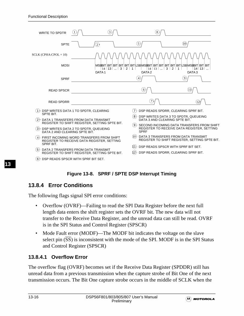
13-16 DSP56F801/803/805/807 User’s Manual�Preliminary
Functional Description
13
Figure 13-8. SPRF / SPTE DSP Interrupt Timing
13.8.4 Error Conditions
The following flags signal SPI error conditions:
• Overflow (OVRF)—Failing to read the SPI Data Register before the next full length data enters the shift register sets the OVRF bit. The new data will not transfer to the Receive Data Register, and the unread data can still be read. OVRF is in the SPI Status and Control Register (SPSCR)
• Mode Fault error (MODF)—The MODF bit indicates the voltage on the slave select pin (SS) is inconsistent with the mode of the SPI. MODF is in the SPI Status and Control Register (SPSCR)
13.8.4.1 Overflow Error
The overflow flag (OVRF) becomes set if the Receive Data Register (SPDDR) still has unread data from a previous transmission when the capture strobe of Bit One of the next transmission occurs. The Bit One capture strobe occurs in the middle of SCLK when the
BIT3
MOSI
SPTE
WRITE TO SPDTR 1
DSP WRITES DATA 2 TO SPDTR, QUEUEING
DSP WRITES DATA 1 TO SPDTR, CLEARING
DATA 1 TRANSFERS FROM DATA TRANSMIT
3
1
2
2
3
5
SPTE BIT.
REGISTER TO SHIFT REGISTER, SETTING SPTE BIT.
SPRF
READ SPSCR
MSBBIT14
BIT13
BIT...
BIT2
BIT1
LSBMSBBIT14
BIT13
BIT...
BIT3
BIT2
BIT1
LSBMSBBIT14
DATA 2 TRANSFERS FROM DATA TRANSMIT
DSP WRITES DATA 3 TO SPDTR, QUEUEING
DATA 3 TRANSFERS FROM DATA TRANSMIT
5
8
10
8
10
4 FIRST INCOMING WORD TRANSFERS FROM SHIFT
6 DSP READS SPSCR WITH SPRF BIT SET.
4
6
9
SECOND INCOMING DATA TRANSFERS FROM SHIFT9
11
DATA 2 AND CLEARING SPTE BIT.
REGISTER TO SHIFT REGISTER, SETTING SPTE BIT.
REGISTER TO RECEIVE DATA REGISTER, SETTINGSPRF BIT.
DATA 3 AND CLEARING SPTE BIT.
REGISTER TO SHIFT REGISTER, SETTING SPTE BIT.
REGISTER TO RECEIVE DATA REGISTER, SETTINGSPRF
12 DSP READS SPDRR, CLEARING SPRF BIT.
BIT13
BIT...
DATA 1 DATA 2 DATA 3
7 12READ SPDRR
7 DSP READS SPDRR, CLEARING SPRF BIT.
11 DSP READS SPSCR WITH SPRF BIT SET.
.
SCLK (CPHA:CPOL = 10)
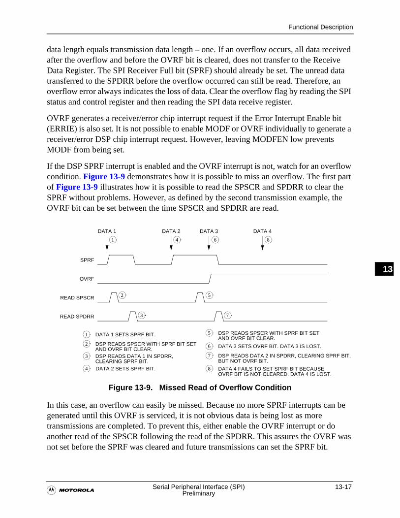
Functional Description
�Serial Peripheral Interface (SPI) 13-17
Preliminary
13
data length equals transmission data length – one. If an overflow occurs, all data received after the overflow and before the OVRF bit is cleared, does not transfer to the Receive Data Register. The SPI Receiver Full bit (SPRF) should already be set. The unread data transferred to the SPDRR before the overflow occurred can still be read. Therefore, an overflow error always indicates the loss of data. Clear the overflow flag by reading the SPI status and control register and then reading the SPI data receive register.
OVRF generates a receiver/error chip interrupt request if the Error Interrupt Enable bit (ERRIE) is also set. It is not possible to enable MODF or OVRF individually to generate a receiver/error DSP chip interrupt request. However, leaving MODFEN low prevents MODF from being set.
If the DSP SPRF interrupt is enabled and the OVRF interrupt is not, watch for an overflow condition. Figure 13-9 demonstrates how it is possible to miss an overflow. The first part of Figure 13-9 illustrates how it is possible to read the SPSCR and SPDRR to clear the SPRF without problems. However, as defined by the second transmission example, the OVRF bit can be set between the time SPSCR and SPDRR are read.
Figure 13-9. Missed Read of Overflow Condition
In this case, an overflow can easily be missed. Because no more SPRF interrupts can be generated until this OVRF is serviced, it is not obvious data is being lost as more transmissions are completed. To prevent this, either enable the OVRF interrupt or do another read of the SPSCR following the read of the SPDRR. This assures the OVRF was not set before the SPRF was cleared and future transmissions can set the SPRF bit.
READ SPDRR
READ SPSCR
OVRF
SPRF
DATA 1 DATA 2 DATA 3 DATA 4
DATA 1 SETS SPRF BIT.
DSP READS SPSCR WITH SPRF BIT SET
DSP READS DATA 1 IN SPDRR,
DATA 2 SETS SPRF BIT.
DSP READS SPSCR WITH SPRF BIT SET
DATA 3 SETS OVRF BIT. DATA 3 IS LOST.
DSP READS DATA 2 IN SPDRR, CLEARING SPRF BIT,
DATA 4 FAILS TO SET SPRF BIT BECAUSE
1
1
2
3
4
5
6
7
8
2
3
4
5
6
7
8
CLEARING SPRF BIT. BUT NOT OVRF BIT.
OVRF BIT IS NOT CLEARED. DATA 4 IS LOST.
AND OVRF BIT CLEAR.
AND OVRF BIT CLEAR.
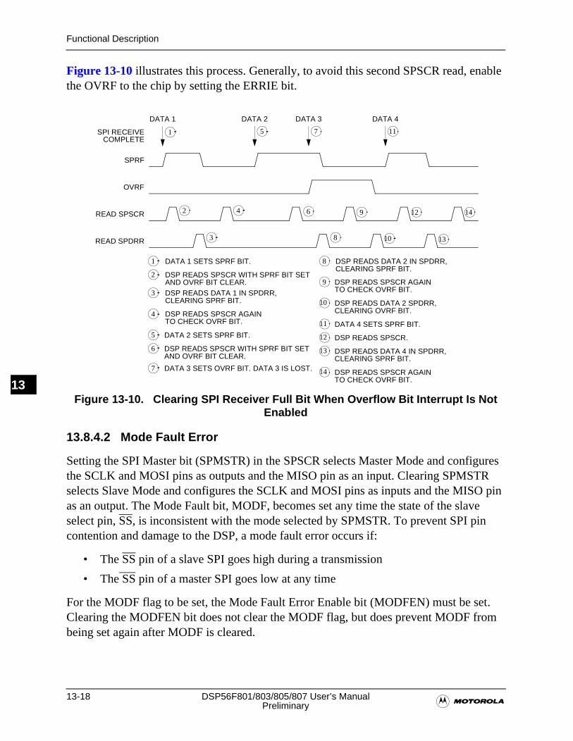
13-18 DSP56F801/803/805/807 User’s Manual�Preliminary
Functional Description
13
Figure 13-10 illustrates this process. Generally, to avoid this second SPSCR read, enable the OVRF to the chip by setting the ERRIE bit.
Figure 13-10. Clearing SPI Receiver Full Bit When Overflow Bit Interrupt Is Not Enabled
13.8.4.2 Mode Fault Error
Setting the SPI Master bit (SPMSTR) in the SPSCR selects Master Mode and configures the SCLK and MOSI pins as outputs and the MISO pin as an input. Clearing SPMSTR selects Slave Mode and configures the SCLK and MOSI pins as inputs and the MISO pin as an output. The Mode Fault bit, MODF, becomes set any time the state of the slave select pin, SS, is inconsistent with the mode selected by SPMSTR. To prevent SPI pin contention and damage to the DSP, a mode fault error occurs if:
• The SS pin of a slave SPI goes high during a transmission
• The SS pin of a master SPI goes low at any time
For the MODF flag to be set, the Mode Fault Error Enable bit (MODFEN) must be set. Clearing the MODFEN bit does not clear the MODF flag, but does prevent MODF from being set again after MODF is cleared.
READ SPDRR
READ SPSCR
OVRF
SPRF
DATA 1 DATA 2 DATA 3 DATA 4
1
DATA 1 SETS SPRF BIT.
DSP READS SPSCR WITH SPRF BIT SET
DSP READS DATA 1 IN SPDRR,
DSP READS SPSCR AGAIN
DATA 2 SETS SPRF BIT.
DSP READS SPSCR WITH SPRF BIT SET
DATA 3 SETS OVRF BIT. DATA 3 IS LOST.
DSP READS DATA 2 IN SPDRR,
DSP READS SPSCR AGAIN
DSP READS DATA 2 SPDRR,
DATA 4 SETS SPRF BIT.
DSP READS SPSCR.
DSP READS DATA 4 IN SPDRR,
DSP READS SPSCR AGAIN
1
2
3CLEARING SPRF BIT.
4TO CHECK OVRF BIT.
5
6
7
8
9
CLEARING SPRF BIT.
TO CHECK OVRF BIT.
10CLEARING OVRF BIT.
11
12
13
14
2
3
4
5
6
7
8
9
10
11
12
13
14
CLEARING SPRF BIT.
TO CHECK OVRF BIT.
SPI RECEIVECOMPLETE
AND OVRF BIT CLEAR.
AND OVRF BIT CLEAR.
Functional Description
�Serial Peripheral Interface (SPI) 13-19
Preliminary
13
MODF generates a receiver/error chip interrupt request if the error interrupt enable bit (ERRIE) is also set. It is not possible to enable MODF or OVRF individually to generate a receiver/error DSP interrupt request. However, leaving MODFEN low prevents MODF from being set.
In a master SPI with the Mode Fault Enable bit (MODFEN) set, the Mode Fault flag (MODF) is set if SS goes to logic zero. A Mode Fault in a master SPI causes the following events to occur:
• If ERRIE = 1, the SPI generates an SPI receiver/error DSP interrupt request
• The SPE bit is cleared (SPI disabled)
• The SPTE bit is set
• The SPI state counter is cleared
When configured as a slave (SPMSTR = 0), the MODF flag is set if the SS goes high during a transmission. When CPHA = 0, a transmission begins when SS goes low and ends once the incoming SCLK goes back to its idle level following the shift of the last data bit. When CPHA = 1, the transmission begins when the SCLK leaves its idle level and SS is already low. The transmission continues until the SCLK returns to its idle level following the shift of the last data bit.
Note: Setting the MODF flag does not clear the SPMSTR bit. The SPMSTR bit has no function when SPE = 0. Reading SPMSTR when MODF = 1 shows the difference between a MODF occurring when the SPI is a master and when it is a slave.
— When CPHA = 0, a MODF occurs if a slave is selected, SS is at logic 0, and later unselected, SS is at logic 1 after the first bit of data has been received (SCLK is toggled at least once). This happens because SS at logic 0 indicates the start of the transmission, MISO driven out with the value of MSB, for CPHA = 0
— When CPHA = 1, a slave can be selected and then later unselected with no transmission occurring. Therefore, MODF does not occur since a transmission was never begun
In a slave SPI (MSTR = 0), the MODF bit generates an SPI receiver/error DSP interrupt request if the ERRIE bit is set. The MODF bit does not clear the SPE bit or reset the SPI in any way. Software can abort the SPI transmission by clearing the SPE bit of the slave.
Note: A logic one voltage on the SS pin of a slave SPI puts the MISO pin in a high impedance state. Also, the slave SPI ignores all incoming SCLK clocks, even if
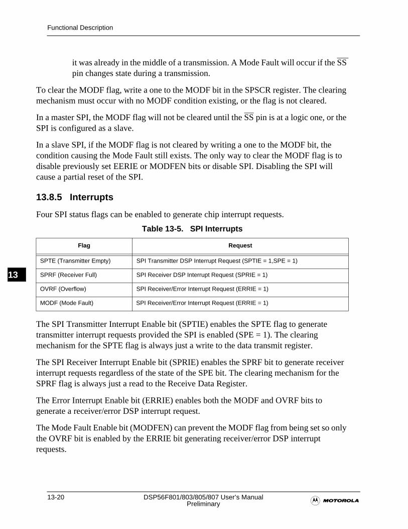
13-20 DSP56F801/803/805/807 User’s Manual�Preliminary
Functional Description
13
it was already in the middle of a transmission. A Mode Fault will occur if the SS pin changes state during a transmission.
To clear the MODF flag, write a one to the MODF bit in the SPSCR register. The clearing mechanism must occur with no MODF condition existing, or the flag is not cleared.
In a master SPI, the MODF flag will not be cleared until the SS pin is at a logic one, or the SPI is configured as a slave.
In a slave SPI, if the MODF flag is not cleared by writing a one to the MODF bit, the condition causing the Mode Fault still exists. The only way to clear the MODF flag is to disable previously set EERIE or MODFEN bits or disable SPI. Disabling the SPI will cause a partial reset of the SPI.
13.8.5 Interrupts
Four SPI status flags can be enabled to generate chip interrupt requests.
The SPI Transmitter Interrupt Enable bit (SPTIE) enables the SPTE flag to generate transmitter interrupt requests provided the SPI is enabled (SPE = 1). The clearing mechanism for the SPTE flag is always just a write to the data transmit register.
The SPI Receiver Interrupt Enable bit (SPRIE) enables the SPRF bit to generate receiver interrupt requests regardless of the state of the SPE bit. The clearing mechanism for the SPRF flag is always just a read to the Receive Data Register.
The Error Interrupt Enable bit (ERRIE) enables both the MODF and OVRF bits to generate a receiver/error DSP interrupt request.
The Mode Fault Enable bit (MODFEN) can prevent the MODF flag from being set so only the OVRF bit is enabled by the ERRIE bit generating receiver/error DSP interrupt requests.
Table 13-5. SPI Interrupts
Flag Request
SPTE (Transmitter Empty) SPI Transmitter DSP Interrupt Request (SPTIE = 1,SPE = 1)
SPRF (Receiver Full) SPI Receiver DSP Interrupt Request (SPRIE = 1)
OVRF (Overflow) SPI Receiver/Error Interrupt Request (ERRIE = 1)
MODF (Mode Fault) SPI Receiver/Error Interrupt Request (ERRIE = 1)
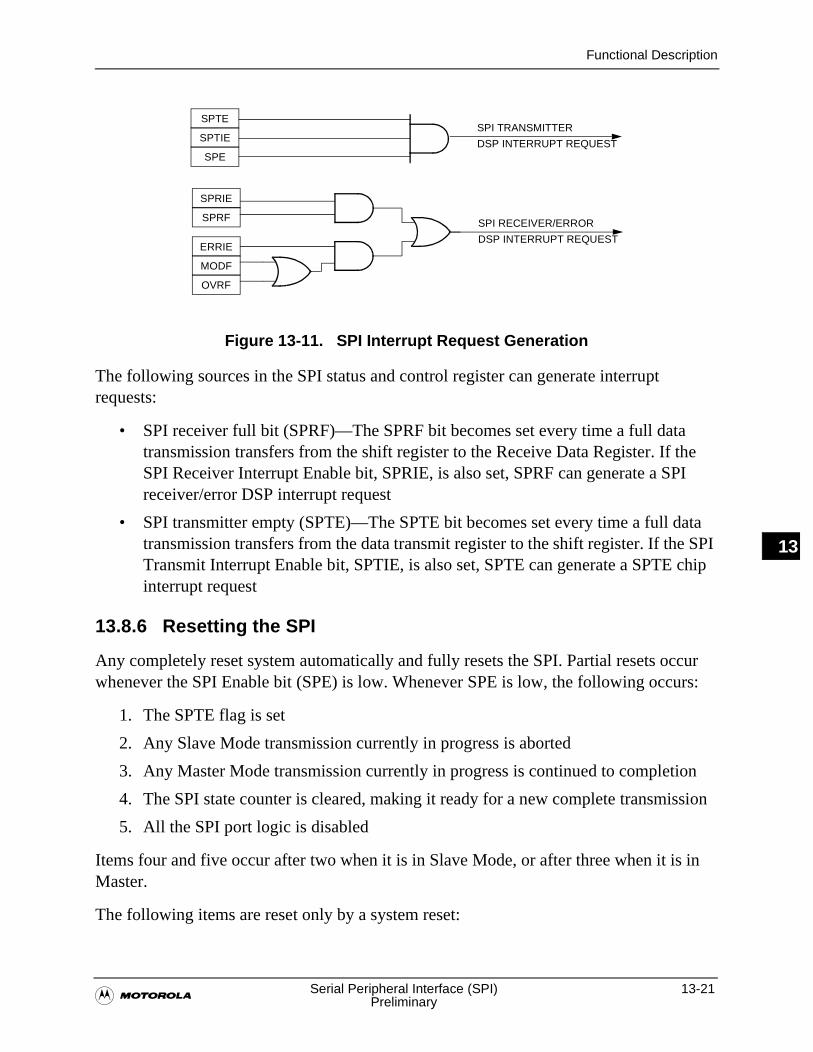
Functional Description
�Serial Peripheral Interface (SPI) 13-21
Preliminary
13
Figure 13-11. SPI Interrupt Request Generation
The following sources in the SPI status and control register can generate interrupt requests:
• SPI receiver full bit (SPRF)—The SPRF bit becomes set every time a full data transmission transfers from the shift register to the Receive Data Register. If the SPI Receiver Interrupt Enable bit, SPRIE, is also set, SPRF can generate a SPI receiver/error DSP interrupt request
• SPI transmitter empty (SPTE)—The SPTE bit becomes set every time a full data transmission transfers from the data transmit register to the shift register. If the SPI Transmit Interrupt Enable bit, SPTIE, is also set, SPTE can generate a SPTE chip interrupt request
13.8.6 Resetting the SPI
Any completely reset system automatically and fully resets the SPI. Partial resets occur whenever the SPI Enable bit (SPE) is low. Whenever SPE is low, the following occurs:
1. The SPTE flag is set
2. Any Slave Mode transmission currently in progress is aborted
3. Any Master Mode transmission currently in progress is continued to completion
4. The SPI state counter is cleared, making it ready for a new complete transmission
5. All the SPI port logic is disabled
Items four and five occur after two when it is in Slave Mode, or after three when it is in Master.
The following items are reset only by a system reset:
SPTE
SPTIE
SPRF
SPRIE
ERRIE
MODF
OVRF
SPE
SPI TRANSMITTER
DSP INTERRUPT REQUEST
SPI RECEIVER/ERROR
DSP INTERRUPT REQUEST
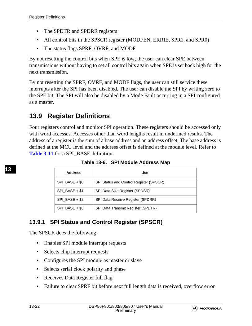
13-22 DSP56F801/803/805/807 User’s Manual�Preliminary
Register Definitions
13
• The SPDTR and SPDRR registers
• All control bits in the SPSCR register (MODFEN, ERRIE, SPR1, and SPR0)
• The status flags SPRF, OVRF, and MODF
By not resetting the control bits when SPE is low, the user can clear SPE between transmissions without having to set all control bits again when SPE is set back high for the next transmission.
By not resetting the SPRF, OVRF, and MODF flags, the user can still service these interrupts after the SPI has been disabled. The user can disable the SPI by writing zero to the SPE bit. The SPI will also be disabled by a Mode Fault occurring in a SPI configured as a master.
13.9 Register Definitions
Four registers control and monitor SPI operation. These registers should be accessed only with word accesses. Accesses other than word lengths result in undefined results. The address of a register is the sum of a base address and an address offset. The base address is defined at the MCU level and the address offset is defined at the module level. Refer to Table 3-11 for a SPI_BASE definition.
13.9.1 SPI Status and Control Register (SPSCR)
The SPSCR does the following:
• Enables SPI module interrupt requests
• Selects chip interrupt requests
• Configures the SPI module as master or slave
• Selects serial clock polarity and phase
• Receives Data Register full flag
• Failure to clear SPRF bit before next full length data is received, overflow error
Table 13-6. SPI Module Address Map
Address Use
SPI_BASE + $0 SPI Status and Control Register (SPSCR)
SPI_BASE + $1 SPI Data Size Register (SPDSR)
SPI_BASE + $2 SPI Data Receive Register (SPDRR)
SPI_BASE + $3 SPI Data Transmit Register (SPDTR)
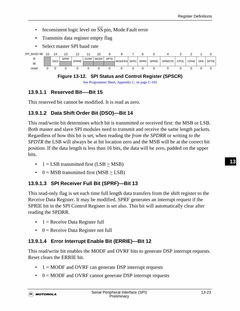
Register Definitions
�Serial Peripheral Interface (SPI) 13-23
Preliminary
13
• Inconsistent logic level on SS pin, Mode Fault error
• Transmits data register empty flag
• Select master SPI baud rate
13.9.1.1 Reserved Bit----Bit 15
This reserved bit cannot be modified. It is read as zero.
13.9.1.2 Data Shift Order Bit (DSO)—Bit 14
This read/write bit determines which bit is transmitted or received first: the MSB or LSB. Both master and slave SPI modules need to transmit and receive the same length packets. Regardless of how this bit is set, when reading the from the SPDRR or writing to the SPDTR the LSB will always be at bit location zero and the MSB will be at the correct bit position. If the data length is less than 16 bits, the data will be zero, padded on the upper bits.
• 1 = LSB transmitted first (LSB > MSB)
• 0 = MSB transmitted first (MSB > LSB)
13.9.1.3 SPI Receiver Full Bit (SPRF)—Bit 13
This read-only flag is set each time full length data transfers from the shift register to the Receive Data Register. It may be modified. SPRF generates an interrupt request if the SPRIE bit in the SPI Control Register is set also. This bit will automatically clear after reading the SPDRR.
• 1 = Receive Data Register full
• 0 = Receive Data Register not full
13.9.1.4 Error Interrupt Enable Bit (ERRIE)—Bit 12
This read/write bit enables the MODF and OVRF bits to generate DSP interrupt requests. Reset clears the ERRIE bit.
• 1 = MODF and OVRF can generate DSP interrupt requests
• 0 = MODF and OVRF cannot generate DSP interrupt requests
SPI_BASE+$0 15 14 13 12 11 10 9 8 7 6 5 4 3 2 1 0
RDSO
SPRFERRIE
OVRF MODF SPTEMODFEN SPR1 SPR0 SPRIE SPMSTR CPOL CPHA SPE SPTIE
W
reset 0 0 0 0 0 0 0 0 0 0 0 0 0 0 0 0
Figure 13-12. SPI Status and Control Register (SPSCR)See Programmer Sheet, Appendix C, on page C-103
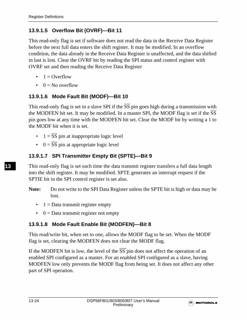
13-24 DSP56F801/803/805/807 User’s Manual�Preliminary
Register Definitions
13
13.9.1.5 Overflow Bit (OVRF)—Bit 11
This read-only flag is set if software does not read the data in the Receive Data Register before the next full data enters the shift register. It may be modified. In an overflow condition, the data already in the Receive Data Register is unaffected, and the data shifted in last is lost. Clear the OVRF bit by reading the SPI status and control register with OVRF set and then reading the Receive Data Register
• 1 = Overflow
• 0 = No overflow
13.9.1.6 Mode Fault Bit (MODF)—Bit 10
This read-only flag is set in a slave SPI if the SS pin goes high during a transmission with the MODFEN bit set. It may be modified. In a master SPI, the MODF flag is set if the SS pin goes low at any time with the MODFEN bit set. Clear the MODF bit by writing a 1 to the MODF bit when it is set.
• 1 = SS pin at inappropriate logic level
• 0 = SS pin at appropriate logic level
13.9.1.7 SPI Transmitter Empty Bit (SPTE)—Bit 9
This read-only flag is set each time the data transmit register transfers a full data length into the shift register. It may be modified. SPTE generates an interrupt request if the SPTIE bit in the SPI control register is set also.
Note: Do not write to the SPI Data Register unless the SPTE bit is high or data may be lost.
• 1 = Data transmit register empty
• 0 = Data transmit register not empty
13.9.1.8 Mode Fault Enable Bit (MODFEN)—Bit 8
This read/write bit, when set to one, allows the MODF flag to be set. When the MODF flag is set, clearing the MODFEN does not clear the MODF flag.
If the MODFEN bit is low, the level of the SS pin does not affect the operation of an enabled SPI configured as a master. For an enabled SPI configured as a slave, having MODFEN low only prevents the MODF flag from being set. It does not affect any other part of SPI operation.
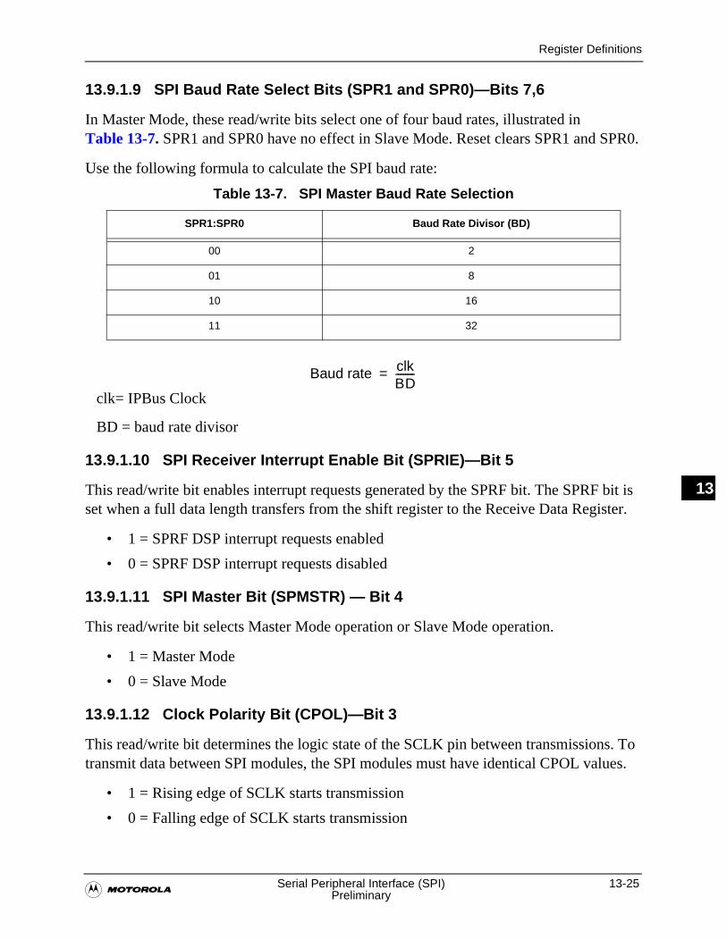
Register Definitions
�Serial Peripheral Interface (SPI) 13-25
Preliminary
13
13.9.1.9 SPI Baud Rate Select Bits (SPR1 and SPR0)—Bits 7,6
In Master Mode, these read/write bits select one of four baud rates, illustrated in Table 13-7. SPR1 and SPR0 have no effect in Slave Mode. Reset clears SPR1 and SPR0.
Use the following formula to calculate the SPI baud rate:
clk= IPBus Clock
BD = baud rate divisor
13.9.1.10 SPI Receiver Interrupt Enable Bit (SPRIE)—Bit 5
This read/write bit enables interrupt requests generated by the SPRF bit. The SPRF bit is set when a full data length transfers from the shift register to the Receive Data Register.
• 1 = SPRF DSP interrupt requests enabled
• 0 = SPRF DSP interrupt requests disabled
13.9.1.11 SPI Master Bit (SPMSTR) — Bit 4
This read/write bit selects Master Mode operation or Slave Mode operation.
• 1 = Master Mode
• 0 = Slave Mode
13.9.1.12 Clock Polarity Bit (CPOL)—Bit 3
This read/write bit determines the logic state of the SCLK pin between transmissions. To transmit data between SPI modules, the SPI modules must have identical CPOL values.
• 1 = Rising edge of SCLK starts transmission
• 0 = Falling edge of SCLK starts transmission
Table 13-7. SPI Master Baud Rate Selection
SPR1:SPR0 Baud Rate Divisor (BD)
00 2
01 8
10 16
11 32
Baud rate clkBD--------=
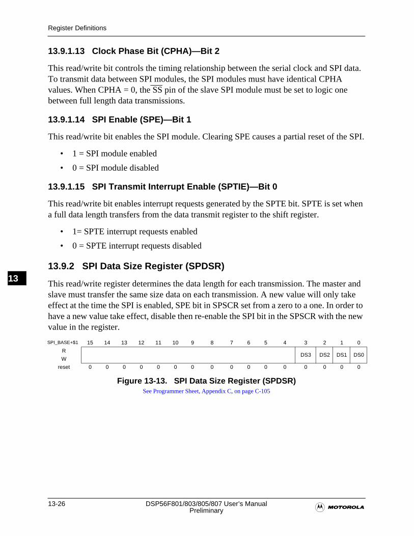
13-26 DSP56F801/803/805/807 User’s Manual�Preliminary
Register Definitions
13
13.9.1.13 Clock Phase Bit (CPHA)—Bit 2
This read/write bit controls the timing relationship between the serial clock and SPI data. To transmit data between SPI modules, the SPI modules must have identical CPHA values. When CPHA = 0, the SS pin of the slave SPI module must be set to logic one between full length data transmissions.
13.9.1.14 SPI Enable (SPE)—Bit 1
This read/write bit enables the SPI module. Clearing SPE causes a partial reset of the SPI.
• 1 = SPI module enabled
• 0 = SPI module disabled
13.9.1.15 SPI Transmit Interrupt Enable (SPTIE)—Bit 0
This read/write bit enables interrupt requests generated by the SPTE bit. SPTE is set when a full data length transfers from the data transmit register to the shift register.
• 1= SPTE interrupt requests enabled
• 0 = SPTE interrupt requests disabled
13.9.2 SPI Data Size Register (SPDSR)
This read/write register determines the data length for each transmission. The master and slave must transfer the same size data on each transmission. A new value will only take effect at the time the SPI is enabled, SPE bit in SPSCR set from a zero to a one. In order to have a new value take effect, disable then re-enable the SPI bit in the SPSCR with the new value in the register.
SPI_BASE+$1 15 14 13 12 11 10 9 8 7 6 5 4 3 2 1 0
RDS3 DS2 DS1 DS0
W
reset 0 0 0 0 0 0 0 0 0 0 0 0 0 0 0 0
Figure 13-13. SPI Data Size Register (SPDSR)See Programmer Sheet, Appendix C, on page C-105
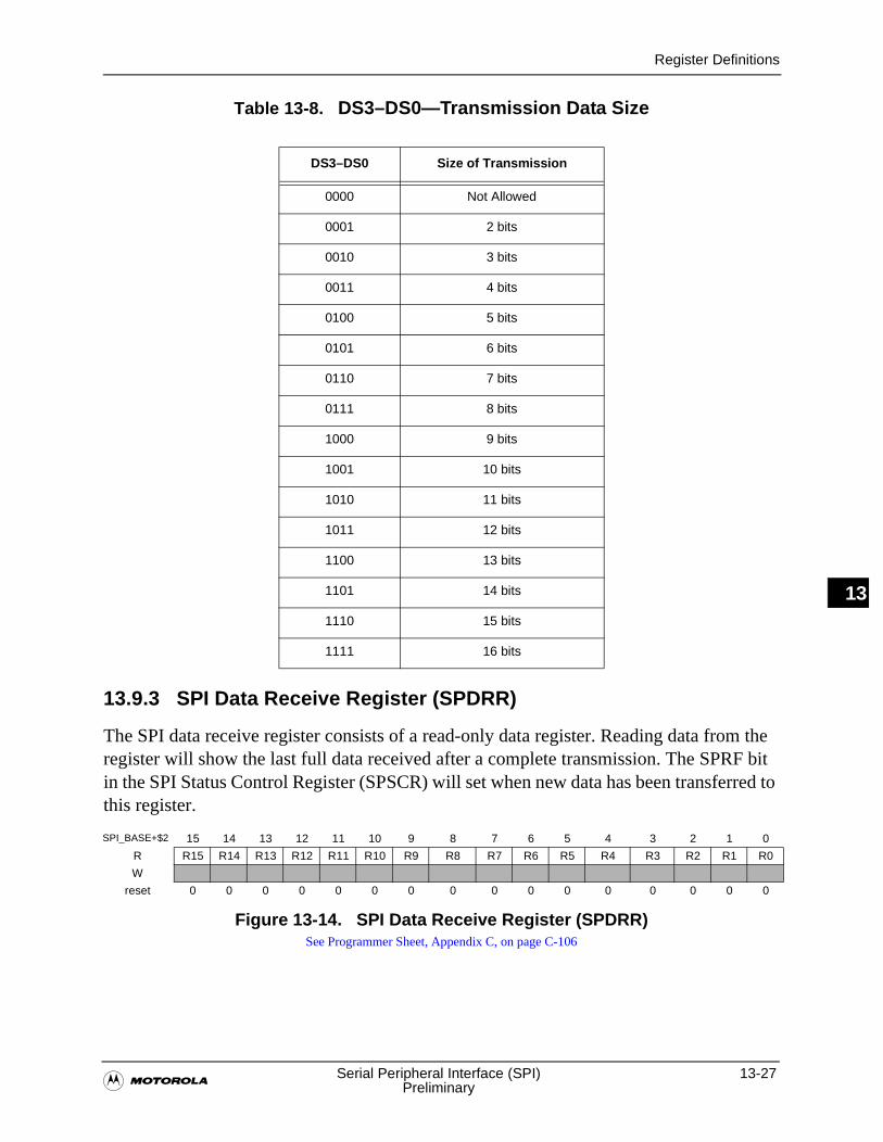
Register Definitions
�Serial Peripheral Interface (SPI) 13-27
Preliminary
13
Table 13-8. DS3–DS0—Transmission Data Size
13.9.3 SPI Data Receive Register (SPDRR)
The SPI data receive register consists of a read-only data register. Reading data from the register will show the last full data received after a complete transmission. The SPRF bit in the SPI Status Control Register (SPSCR) will set when new data has been transferred to this register.
DS3–DS0 Size of Transmission
0000 Not Allowed
0001 2 bits
0010 3 bits
0011 4 bits
0100 5 bits
0101 6 bits
0110 7 bits
0111 8 bits
1000 9 bits
1001 10 bits
1010 11 bits
1011 12 bits
1100 13 bits
1101 14 bits
1110 15 bits
1111 16 bits
SPI_BASE+$2 15 14 13 12 11 10 9 8 7 6 5 4 3 2 1 0
R R15 R14 R13 R12 R11 R10 R9 R8 R7 R6 R5 R4 R3 R2 R1 R0
W
reset 0 0 0 0 0 0 0 0 0 0 0 0 0 0 0 0
Figure 13-14. SPI Data Receive Register (SPDRR)See Programmer Sheet, Appendix C, on page C-106
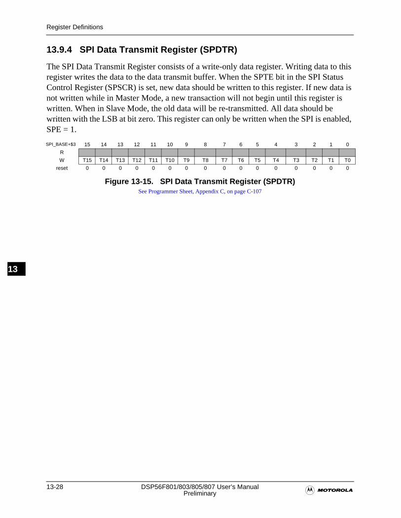
13-28 DSP56F801/803/805/807 User’s Manual�Preliminary
Register Definitions
13
13.9.4 SPI Data Transmit Register (SPDTR)
The SPI Data Transmit Register consists of a write-only data register. Writing data to this register writes the data to the data transmit buffer. When the SPTE bit in the SPI Status Control Register (SPSCR) is set, new data should be written to this register. If new data is not written while in Master Mode, a new transaction will not begin until this register is written. When in Slave Mode, the old data will be re-transmitted. All data should be written with the LSB at bit zero. This register can only be written when the SPI is enabled, SPE = 1.
SPI_BASE+$3 15 14 13 12 11 10 9 8 7 6 5 4 3 2 1 0
R
W T15 T14 T13 T12 T11 T10 T9 T8 T7 T6 T5 T4 T3 T2 T1 T0
reset 0 0 0 0 0 0 0 0 0 0 0 0 0 0 0 0
Figure 13-15. SPI Data Transmit Register (SPDTR)See Programmer Sheet, Appendix C, on page C-107
�Quad Timer Module 14-1
Preliminary
14
Chapter 14Quad Timer Module

14-2 DSP56F801/803/805/807 User’s Manual�Preliminary
14
Introduction
�Quad Timer Module 14-3
Preliminary
14
14.1 Introduction
There are up to four different possible Quad Timer Modules on the different configurations of the DSP56F800 series. The DSP56F801 has two Quad Timer Modules, C and D, while the DSP56F803/805/807 have four Quad Timer Modules: A, B, C, and D. Timer Modules C and D have dedicated pins. Timer Module C has two dedicated pins on the 805/807. Timer Modules A and B share pins with the Quadrature decoder modules.
Each timer module contains four identical counter/timer groups. Each 16-bit counter timer group contains a prescaler, a counter, a load register, a hold register, a capture register, two compare registers, a status and control register, and a control register. All of the registers except the prescaler are read/write registers.
Note: This document uses the terms timer and counter interchangeably because the counter/timers may perform either or both tasks.
The prescaler provides different time bases useful for clocking the counter/timer. The counter provides the ability to count internal or external events. The Load register provides the initialization value to the counter when the counter’s terminal value has been reached. The Hold register captures the counter’s value when other counters are being read. This feature supports the reading of cascaded counters. The Capture register implements an external signal to take a snapshot of the counter’s current value. The Compare registers provide the values enabling counters to be compared. If a match occurs, the OFLAG signal can be set, cleared, or toggled. At match time, an interrupt is generated if enabled. Within a time module, a set of four counters/timers, the input pins are apportioned.This document uses the terms timer and counter interchangeably because the counter/timers may perform either or both tasks.
The prescaler provides different time bases useful for clocking the counter/timer. The counter provides the ability to count internal or external events. The Load register provides the initialization value to the counter when the counter’s terminal value has been reached. The Hold register captures the counter’s value when other counters are being read. This feature supports the reading of cascaded counters. The Capture register enables an external signal to take a snapshot of the counter’s current value. The Compare registers provide values counters for comparison purposes. If a match occurs, the OFLAG signal can be set, cleared, or toggled. At match time, an interrupt is generated if enabled. Within a timer module, a set of four counters/timers, the input pins may be shared.
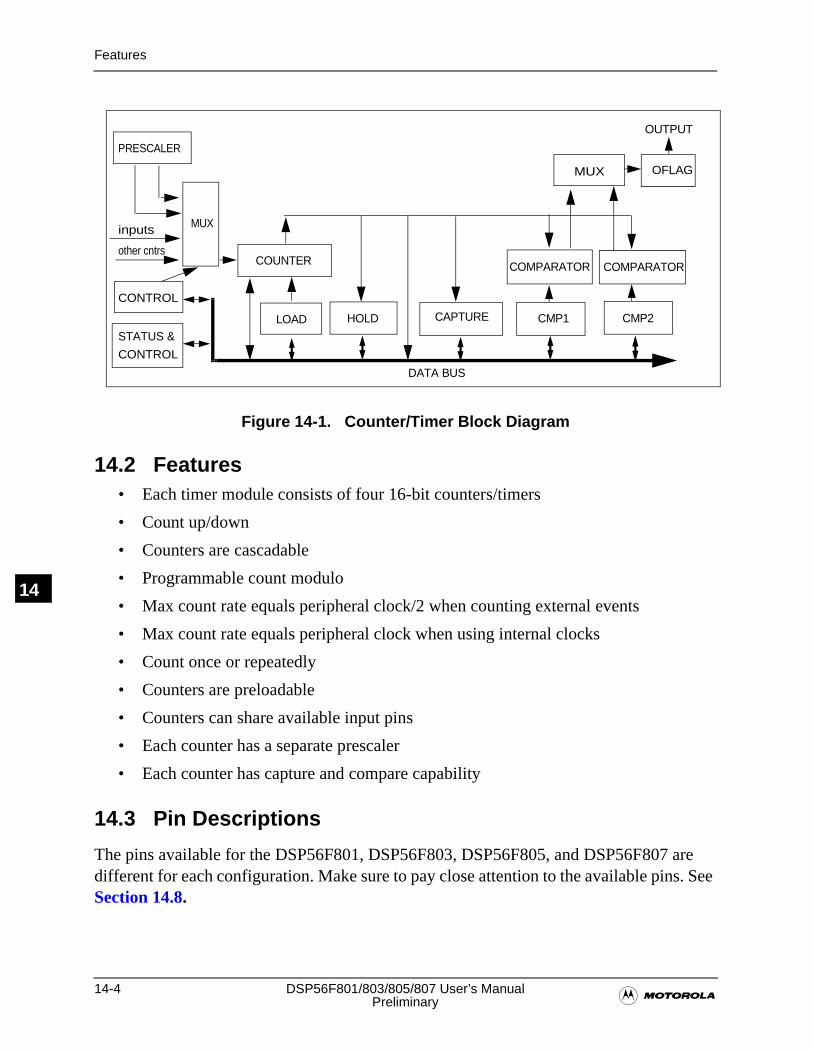
14-4 DSP56F801/803/805/807 User’s Manual�Preliminary
Features
14
Figure 14-1. Counter/Timer Block Diagram
14.2 Features• Each timer module consists of four 16-bit counters/timers
• Count up/down
• Counters are cascadable
• Programmable count modulo
• Max count rate equals peripheral clock/2 when counting external events
• Max count rate equals peripheral clock when using internal clocks
• Count once or repeatedly
• Counters are preloadable
• Counters can share available input pins
• Each counter has a separate prescaler
• Each counter has capture and compare capability
14.3 Pin Descriptions
The pins available for the DSP56F801, DSP56F803, DSP56F805, and DSP56F807 are different for each configuration. Make sure to pay close attention to the available pins. See Section 14.8.
COUNTER
LOAD HOLD CMP1
MUX OFLAG
MUX
PRESCALER
OUTPUT
STATUS &
CONTROL
CAPTURE
inputs
other cntrs
CMP2
COMPARATOR COMPARATOR
CONTROL
DATA BUS
Functional Description
�Quad Timer Module 14-5
Preliminary
14
14.4 Register Summary
A prefix is added to each register reflecting the Quad Timer module and channel is being accessed: TMRA0, TMRA1, TMRA2, TMRA3, TMRB0, TMRB1, TMRB2, TMRB3, TMRC0, TMRC1, TMRC2, TMRC3, TMRD0, TMRD1, TMRD2, TMRD3. For example, the CNTR Register for the Quad Timer A, channel zero (TMRA0) module will be called TMRA0_CNTR. Each timer/counter in the DSP56F801/803/805/807 has the following registers:
• Quad Timer Counter (CNTR)
• Quad Timer Load Register (LOAD)
• Quad Timer Hold Register (HOLD)
• Quad Timer Capture Register (CAP)
• Quad Timer Compare Registers (CMP1 and CMP2)
• Quad Timer Status and Control Register (SCR)
• Quad Timer Control Register (CTRL)
For further information about:
• TMRA registers please refer to Table 3-14
• TMRB registers please refer to Table 3-15
• TMRC registers please refer to Table 3-16
• TMRD registers please refer to Table 3-17
14.5 Functional Description
The counter/timer has two basic modes of operation: it can count internal or external events, or it can count an internal clock source while an external input signal is asserted, thus timing the width of the external input signal.
14.5.1 Counting Options
The counter can count the rising, falling, or both edges of the selected input pin. The counter can decode and count quadrature encoded input signals. The counter can count up and down using dual inputs in a count with direction format. The counter’s terminal count value (modulo) is programmable. The value loaded into the counter after reaching its terminal count is programmable. The counter can count repeatedly, or it can stop after completing one count cycle. The counter can be programmed to count to a programmed value and then immediately re initialize, or it can count through the compare value until the count moves to zero.
14-6 DSP56F801/803/805/807 User’s Manual�Preliminary
Counting Mode Definitions
14
14.5.2 External Inputs
The external inputs to each counter/timer are shareable among each of the four counter/timers within a module. The external inputs can be used as count commands and timer commands. They can trigger the current counter value to be captured and then be used to generate interrupt requests. The polarity of the external inputs are selectable.
14.5.3 OFLAG Output Signal
The primary output of each timer/counter is the output signal OFLAG. The OFLAG output signal can be set, cleared, or toggled when the counter reaches the programmed value. The OFLAG output signal may be outputted to an external pin shared with an external input signal. The OFLAG output signal enables each counter to generate square waves, PWM, or pulse stream outputs. The polarity of the OFLAG output signal is selectable.
14.5.4 Master Signal
Any counter/timer can be assigned as a master. A master’s compare signal can be broadcast to the other counters/timers within a module. The other counters can be configured to re initialize their counters and/or force their OFLAG output signals to predetermined values when a master’s counter/timer compare event occurs.
14.6 Counting Mode Definitions
The selected external count signals are sampled at the module’s base clock rate and then run through a transition detector. The maximum count rate is one-half of the base clock rate. Internal clock sources can be used to clock the counters up to the base clock rate.
If a counter is programmed to count to a specific value and then stop, the Count Mode in the CTRL register is cleared when the count terminates.
14.6.1 Stop Mode
If the Count Mode field is set to 000, the counter is inert. No counting will occur.
14.6.2 Count Mode
If the Count Mode field is set to 001, the counter will count the rising edges of the selected clock source. This mode is useful for counting generating periodic interrupts for timing purposes, or counting external events such as widgets on a conveyor belt passing a sensor. If the selected input is inverted by setting the Input Polarity Select (IPS) bit, then the negative edge of the selected signal is counted.
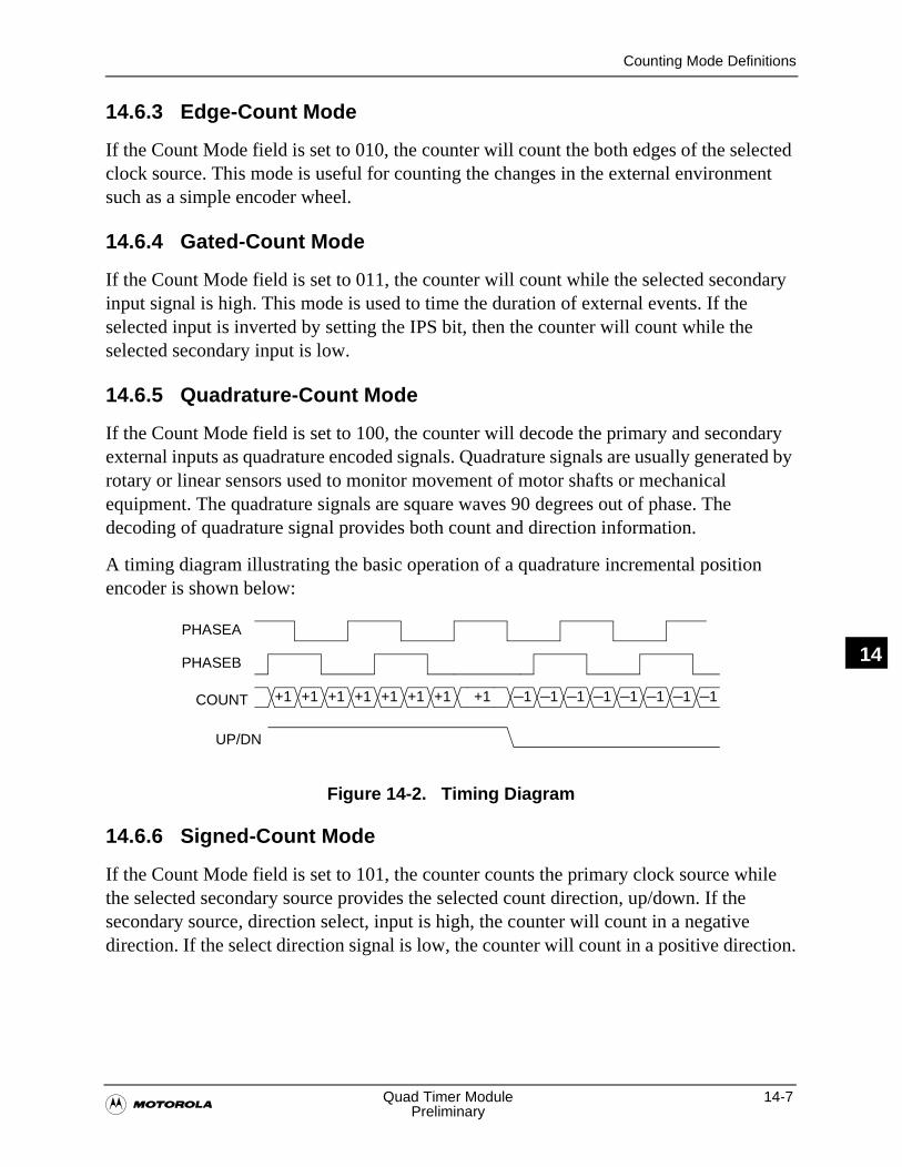
Counting Mode Definitions
�Quad Timer Module 14-7
Preliminary
14
14.6.3 Edge-Count Mode
If the Count Mode field is set to 010, the counter will count the both edges of the selected clock source. This mode is useful for counting the changes in the external environment such as a simple encoder wheel.
14.6.4 Gated-Count Mode
If the Count Mode field is set to 011, the counter will count while the selected secondary input signal is high. This mode is used to time the duration of external events. If the selected input is inverted by setting the IPS bit, then the counter will count while the selected secondary input is low.
14.6.5 Quadrature-Count Mode
If the Count Mode field is set to 100, the counter will decode the primary and secondary external inputs as quadrature encoded signals. Quadrature signals are usually generated by rotary or linear sensors used to monitor movement of motor shafts or mechanical equipment. The quadrature signals are square waves 90 degrees out of phase. The decoding of quadrature signal provides both count and direction information.
A timing diagram illustrating the basic operation of a quadrature incremental position encoder is shown below:
Figure 14-2. Timing Diagram
14.6.6 Signed-Count Mode
If the Count Mode field is set to 101, the counter counts the primary clock source while the selected secondary source provides the selected count direction, up/down. If the secondary source, direction select, input is high, the counter will count in a negative direction. If the select direction signal is low, the counter will count in a positive direction.
+1 +1 +1 +1 +1 +1 +1 +1 –1 –1 –1 –1 –1 –1 –1 –1
PHASEB
COUNT
UP/DN
PHASEA
14-8 DSP56F801/803/805/807 User’s Manual�Preliminary
Counting Mode Definitions
14
14.6.7 Triggered-Count Mode
If the Count Mode field is set to 110, the counter will begin counting the rising edges of the primary clock source after a positive transition of the secondary input occurs. For example, negative edge if IPS = 1. The counting will continue until a compare event occurs or another positive input transition is detected.
14.6.8 One-Shot Mode
If the Count Mode field is set to 110, and the counter is set to re initialize at a compare event, Count Length = 1, and the OFLAG Output Mode is set to 101, cleared on initialization, set on compare, the counter works in a One-Shot Mode. An external event causes the counter to count. When terminal count is reached, the OFLAG output is asserted. This delayed output assertion can be used to provide timing delays. When used with timer C2 or C3, this One-Shot Mode may be used to delay the ADC acquisition of new samples until a specified period of time has passed since the PWM module asserted the synchronized signal.
14.6.9 Cascade-Count Mode
If the Count Mode field is set to 111, the counter is connected to the output of another counter and selected by the primary count source. The counter will count up and down as compare events occur in the selected source counter. This Cascade or Daisy-Chained Mode enables multiple counters to be cascaded to yield longer counter lengths. The Cascade Count Mode uses a special high speed signal path without regarding the state of the OFLAG signal. If the selected source counter experiences a CMP1 compare event while counting in a positive direction, the counter will increment. If the selected source counter experiences a CMP2 compare event while counting in a negative direction, the counter will decrement.
Whenever any counter is read within a counter module, all of the counters’ values within a module are captured in their respective Hold registers. This action supports the reading of a cascaded counter chain. First read any counter of a cascaded counter chain, then read the hold registers of the other counters in the chain. The Cascaded Counter Mode is synchronous.
Note: It is possible to connect counters together by using the other, non-cascade, counter modes and selecting the outputs of other counters as a clock source. In this case, the counters are operating in a ripple mode, where higher order counters will transition a clock later than a purely synchronous design.
Counting Mode Definitions
�Quad Timer Module 14-9
Preliminary
14
14.6.10 Pulse-Output Mode
If the counter is setup for Count Mode (mode = 001), and the OFLAG Output Mode is set to 111, Gated Clock Output, and the Count OnCE bit is set, then the counter will output a pulse stream of pulses with the same frequency of the selected clock source. The number of output pulses is equal to the compare value minus the initialization value. This mode is useful for driving step motor systems.
14.6.11 Fixed-Frequency PWM Mode
If the counter is setup for:
• Count Mode (Mode = 001)
• Count through roll-over (Count Length = 0)
• Continuous count (Count Once = 0)
• OFLAG Output Mode is 110 (set on compare, cleared on initialization)
The counter output then yields a Pulse Width Modulated (PWM) signal with a frequency equal to the count clock frequency divided by 65,536 and a pulse width duty cycle equal to the compare value divided by 65,536. This mode of operation is often used to drive PWM amplifiers used to power motors and inverters.
14.6.12 Variable-Frequency PWM Mode
If the counter is setup for:
• COUNT Mode (Mode = 001)
• Count till compare (Count Length = 1)
• Continuos count (Count Once = 0)
• OFLAG Output Mode is 100 (toggle OFLAG and alternate Compare registers)
The counter output then yields a Pulse Width Modulated (PWM) signal. Its frequency and pulse width are determined by the values programmed into the CMP1 and CMP2 registers, and the input clock frequency. This method of PWM generation has the advantage of allowing almost any desired PWM frequency and/or constant on or off periods. This mode of operation is often used to drive PWM amplifiers used to power motors and inverters.
14.6.13 Usage of Compare Registers
The dual Compare registers (CMP1 & CMP2) provide a bi-directional modulo count capability. The CMP1 register is used when the counter is counting up, and the CMP2
14-10 DSP56F801/803/805/807 User’s Manual�Preliminary
Register Definitions
14
register is used when the counter is counting down. The only exception is alternating Compare Mode.
The CMP1 register should be set to the desired maximum count value or $FFFF to indicate the maximum unsigned value prior to Roll-Over, and the CMP2 register should be set to the maximum negative count value or $0000 to indicate the minimum unsigned value prior to Roll-Under.
If the Output Mode is set to 100, the OFLAG will toggle while using alternating compare registers. In this Variable Frequency PWM Mode, the CMP2 value defines the desired pulse width of the on time, and the CMP1 register defines the off time. The Variable Frequency PWM Mode is defined for positive counting only.
One must be careful when changing CMP1 and CMP2 while the counter is active. If the counter has already passed the new value, it will count to $FFFF or $0000, roll over, and then begin counting toward the new value. The check is for Count = CMPx, not Count > CMP1 or Count < CMP2.
14.6.14 Usage of Capture Register
The Capture register stores a copy of the counter’s value when an input edge positive or negative (if IPS = 1) is detected. Once a capture event occurs, no further updating of the Capture register will occur until the IEF (Input Edge Flag) is cleared by writing a zero to the IEF.
14.7 Register Definitions
The address of a register is the sum of a base address and an address offset. The base address is defined at the MCU level and the address offset is defined at the module level. Please refer to Table 3-11 for the appropriate TMR_BASE definition. The base address given for each register will be either TMRA_BASE, TMRB_BASE, TMRC_BASE, or TMRD_BASE depending on which Quad Timer is being used.
Make certain to check which Quad Timers are available on the chip being used. DSP56F801 has a dedicated Quad Timer D. DSP56F803 has a dedicated Quad Timer D and optional Quad Timer A, multiplexed to the Quadrature Decoder. DSP56F805 and DSP56F807 have two dedicated Quad Timers C and D. Also, they have two optional Quad Timers A and B multiplexed to Quadrature Decoders.
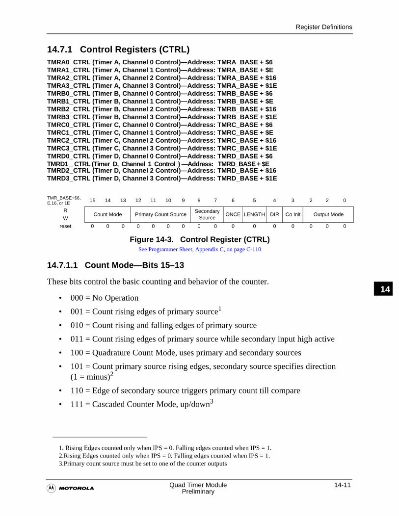
Register Definitions
�Quad Timer Module 14-11
Preliminary
14
14.7.1 Control Registers (CTRL)TMRA0_CTRL (Timer A, Channel 0 Control)—Address: TMRA_BASE + $6TMRA1_CTRL (Timer A, Channel 1 Control)—Address: TMRA_BASE + $ETMRA2_CTRL (Timer A, Channel 2 Control)—Address: TMRA_BASE + $16TMRA3_CTRL (Timer A, Channel 3 Control)—Address: TMRA_BASE + $1ETMRB0_CTRL (Timer B, Channel 0 Control)—Address: TMRB_BASE + $6TMRB1_CTRL (Timer B, Channel 1 Control)—Address: TMRB_BASE + $ETMRB2_CTRL (Timer B, Channel 2 Control)—Address: TMRB_BASE + $16TMRB3_CTRL (Timer B, Channel 3 Control)—Address: TMRB_BASE + $1ETMRC0_CTRL (Timer C, Channel 0 Control)—Address: TMRC_BASE + $6TMRC1_CTRL (Timer C, Channel 1 Control)—Address: TMRC_BASE + $ETMRC2_CTRL (Timer C, Channel 2 Control)—Address: TMRC_BASE + $16TMRC3_CTRL (Timer C, Channel 3 Control)—Address: TMRC_BASE + $1ETMRD0_CTRL (Timer D, Channel 0 Control)—Address: TMRD_BASE + $6TMRD1 _ CTRL (Timer D, Channel 1 Control ) —Address: TMRD_BASE + $ETMRD2_CTRL (Timer D, Channel 2 Control)—Address: TMRD_BASE + $16TMRD3_CTRL (Timer D, Channel 3 Control)—Address: TMRD_BASE + $1E
14.7.1.1 Count Mode—Bits 15–13
These bits control the basic counting and behavior of the counter.
• 000 = No Operation
• 001 = Count rising edges of primary source1
• 010 = Count rising and falling edges of primary source
• 011 = Count rising edges of primary source while secondary input high active
• 100 = Quadrature Count Mode, uses primary and secondary sources
• 101 = Count primary source rising edges, secondary source specifies direction (1 = minus)2
• 110 = Edge of secondary source triggers primary count till compare
• 111 = Cascaded Counter Mode, up/down3
TMR_BASE+$6,E,16, or 1E 15 14 13 12 11 10 9 8 7 6 5 4 3 2 2 0
RCount Mode Primary Count Source
Secondary Source
ONCE LENGTH DIR Co Init Output ModeW
reset 0 0 0 0 0 0 0 0 0 0 0 0 0 0 0 0
Figure 14-3. Control Register (CTRL)See Programmer Sheet, Appendix C, on page C-110
1. Rising Edges counted only when IPS = 0. Falling edges counted when IPS = 1.2.Rising Edges counted only when IPS = 0. Falling edges counted when IPS = 1.3.Primary count source must be set to one of the counter outputs
14-12 DSP56F801/803/805/807 User’s Manual�Preliminary
Register Definitions
14
14.7.1.2 Primary Count Source—Bits 12–9
These bits select the primary count source.
• 0000 = Counter #0 input pin
• 0001 = Counter #1 input pin
• 0010 = Counter #2 input pin
• 0011 = Counter #3 input pin
• 0100 = Counter #0 output
• 0101 = Counter #1 output
• 0110 = Counter #2 output
• 0111 = Counter #3 output
• 1000 = Prescaler (IPBus clock divide by 1)
• 1001 = Prescaler (IPBus clock divide by 2)
• 1010 = Prescaler (IPBus clock divide by 4)
• 1011 = Prescaler (IPBus clock divide by 8)
• 1100 = Prescaler (IPBus clock divide by 16)
• 1101 = Prescaler (IPBus clock divide by 32)
• 1110 = Prescaler (IPBus clock divide by 64)
• 1111 = Prescaler (IPBus clock divide by 128)
Note: A timer selecting its own output for input is not a legal choice. The result is no counting.
Register Definitions
�Quad Timer Module 14-13
Preliminary
14
14.7.1.3 Secondary Count Source—Bits 8–7
These bits provide additional information, such as direction, used for counting.
• 00 = Counter #0 input pin
• 01 = Counter #1 input pin
• 10 = Counter #2 input pin
• 11 = Counter #3 input pin
14.7.1.4 Count Once (ONCE)—Bit 6
This bit selects continuous or one shot counting mode.
• 0 = Count repeatedly
• 1 = Count until compare and then stop. If counting up, successful compare occurs when counter reaches CMP1 value. If counting down, successful compare occurs when counter reaches CMP2 value
14.7.1.5 Count Length (LENGTH)—Bit 5
This bit determines whether the counter counts to the compare value and then reinitializes itself to the value specified in the load register, or the counter continues counting past the compare value, the binary roll over.
• 0 = Roll Over
• 1 = Count until compare, then re initialize. If counting up, successful compare occurs when counter reaches CMP1 value. If counting down, successful compare occurs when counter reaches CMP2 value.4
14.7.1.6 Count Direction (DIR)—Bit 4
This bit selects either the normal count direction up, or the reverse direction, down.
• 0 = Count Up
• 1 = Count Down
14.7.1.7 Co-channel Initialization (Co Init)—Bit 3
This bit enables another counter/timer within the module to force the reinitialization of this counter/timer when it has an active compare event.
4. When output mode $4 is used, alternating values of CMP1 and CMP2 are used to generate successful compares. For example, when output mode is $4, the counter counts until CMP1 value is reached, reinitial-izes, then counts until CMP2 value is reached, reinitializes, then counts until CMP1 value is reached, etc.
14-14 DSP56F801/803/805/807 User’s Manual�Preliminary
Register Definitions
14
• 0 = Co-channel counter/timers can not force a reinitialization of this counter/timer
• 1 = Co-channel counter/timers may force a reinitialization of this counter/timer
14.7.1.8 Output Mode—Bits 2-0
These bits determine the mode of operation for the OFLAG output signal.
• 000 = Asserted while counter is active
• 001 = Clear OFLAG output on successful compare
• 010 = Set OFLAG output on successful compare
• 011 = Toggle OFLAG output on successful compare
• 100 = Toggle OFLAG output using alternating compare registers
• 101 = Set on compare, cleared on secondary source input edge
• 110 = Set on compare, cleared on counter rollover
• 111 = Enable Gated Clock output while counter is active5
5.
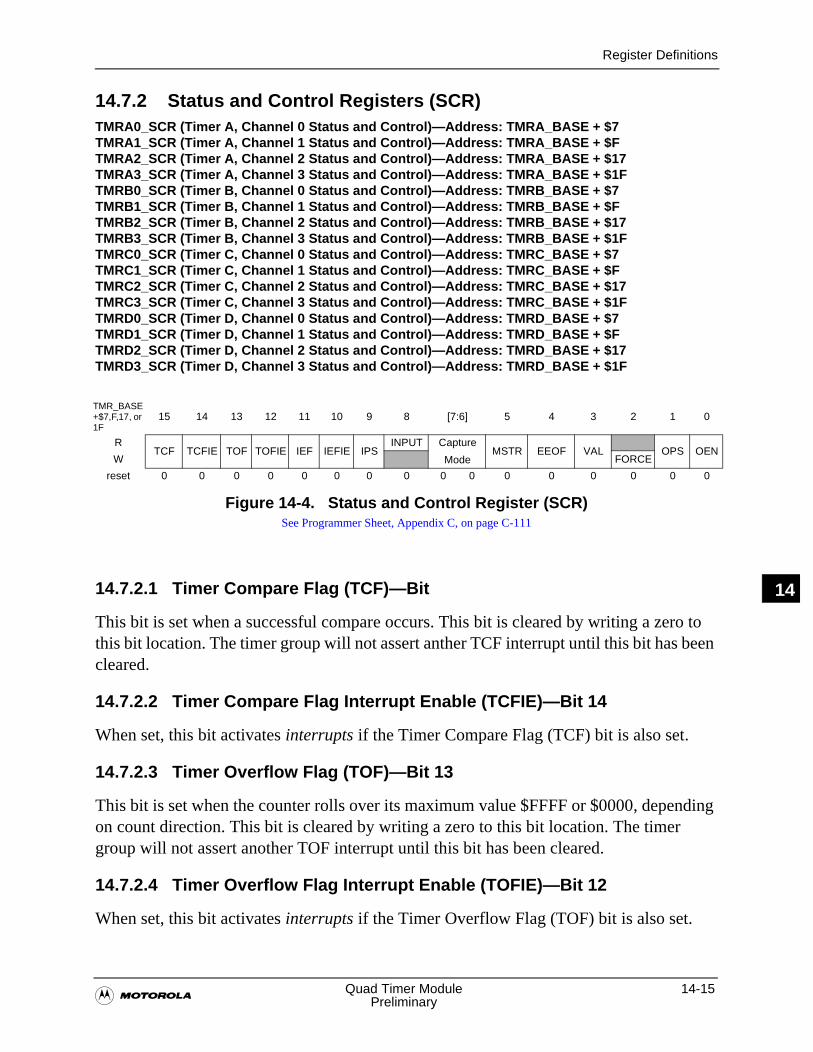
Register Definitions
�Quad Timer Module 14-15
Preliminary
14
14.7.2 Status and Control Registers (SCR)TMRA0_SCR (Timer A, Channel 0 Status and Control)—Address: TMRA_BASE + $7TMRA1_SCR (Timer A, Channel 1 Status and Control)—Address: TMRA_BASE + $FTMRA2_SCR (Timer A, Channel 2 Status and Control)—Address: TMRA_BASE + $17TMRA3_SCR (Timer A, Channel 3 Status and Control)—Address: TMRA_BASE + $1FTMRB0_SCR (Timer B, Channel 0 Status and Control)—Address: TMRB_BASE + $7TMRB1_SCR (Timer B, Channel 1 Status and Control)—Address: TMRB_BASE + $FTMRB2_SCR (Timer B, Channel 2 Status and Control)—Address: TMRB_BASE + $17TMRB3_SCR (Timer B, Channel 3 Status and Control)—Address: TMRB_BASE + $1FTMRC0_SCR (Timer C, Channel 0 Status and Control)—Address: TMRC_BASE + $7TMRC1_SCR (Timer C, Channel 1 Status and Control)—Address: TMRC_BASE + $FTMRC2_SCR (Timer C, Channel 2 Status and Control)—Address: TMRC_BASE + $17TMRC3_SCR (Timer C, Channel 3 Status and Control)—Address: TMRC_BASE + $1FTMRD0_SCR (Timer D, Channel 0 Status and Control)—Address: TMRD_BASE + $7TMRD1_SCR (Timer D, Channel 1 Status and Control)—Address: TMRD_BASE + $FTMRD2_SCR (Timer D, Channel 2 Status and Control)—Address: TMRD_BASE + $17TMRD3_SCR (Timer D, Channel 3 Status and Control)—Address: TMRD_BASE + $1F
14.7.2.1 Timer Compare Flag (TCF)—Bit
This bit is set when a successful compare occurs. This bit is cleared by writing a zero to this bit location. The timer group will not assert anther TCF interrupt until this bit has been cleared.
14.7.2.2 Timer Compare Flag Interrupt Enable (TCFIE)—Bit 14
When set, this bit activates interrupts if the Timer Compare Flag (TCF) bit is also set.
14.7.2.3 Timer Overflow Flag (TOF)—Bit 13
This bit is set when the counter rolls over its maximum value $FFFF or $0000, depending on count direction. This bit is cleared by writing a zero to this bit location. The timer group will not assert another TOF interrupt until this bit has been cleared.
14.7.2.4 Timer Overflow Flag Interrupt Enable (TOFIE)—Bit 12
When set, this bit activates interrupts if the Timer Overflow Flag (TOF) bit is also set.
TMR_BASE+$7,F,17, or 1F
15 14 13 12 11 10 9 8 [7:6] 5 4 3 2 1 0
RTCF TCFIE TOF TOFIE IEF IEFIE IPS
INPUT Capture
ModeMSTR EEOF VAL OPS OEN
W FORCE
reset 0 0 0 0 0 0 0 0 0 0 0 0 0 0 0 0
Figure 14-4. Status and Control Register (SCR)See Programmer Sheet, Appendix C, on page C-111
14-16 DSP56F801/803/805/807 User’s Manual�Preliminary
Register Definitions
14
14.7.2.5 Input Edge Flag (IEF)—Bit 11
This bit is set when a positive input transition occurs. This bit is cleared by writing a zero to this bit position.
Note: Setting the Input Polarity Select (IPS) bit enables the detection of negative input edge transition detection. Also, the control register’s secondary count source determines which external input pin is monitored by the detection circuitry.
14.7.2.6 Input Edge Flag Interrupt Enable (IEFIE)—Bit 10
When set, this bit enables interrupts when the Input Edge Flag (IEF) bit is also set. The timer group will not assert another IEF interrupt until this bit has been cleared.
14.7.2.7 Input Polarity Select (IPS)—Bit 9
When set, this bit inverts the polarity of a signal being driven on to a package pin from an external source. It does not invert the polarity of an input signal when the signal is being driven by another timer group.
14.7.2.8 External Input Signal (INPUT)—Bit 8
This bit reflects the current state of the external input pin after application of the Input Polarity Select (IPS) bit. This is a read only bit.
14.7.2.9 Input Capture Mode (Capture Mode)—Bits 7–6
These bits specify the operation of the capture register as well as the operation of the input edge flag. The Input Capture Mode bits seven to six must be 01, 10 or 11 in order for input edge flag interrupts to be asserted.
• 00 = Capture function is disabled and input edge flag interrupts are disabled
• 01 = Load the Capture register on rising edge of the secondary input source
• 10 = Load the Capture register on falling edge of the secondary input source
• 11 = Load the Capture register on both edges of the secondary input source
14.7.2.10 Master Mode (MSTR)—Bit 5
When set, this bit enables the compare function’s output to be broadcast to the other counters/timers in the module. This signal then can be used to re initialize the other counters and/or force their OFLAG signal outputs.
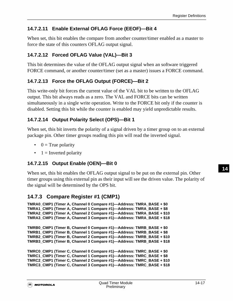
Register Definitions
�Quad Timer Module 14-17
Preliminary
14
14.7.2.11 Enable External OFLAG Force (EEOF)—Bit 4
When set, this bit enables the compare from another counter/timer enabled as a master to force the state of this counters OFLAG output signal.
14.7.2.12 Forced OFLAG Value (VAL)—Bit 3
This bit determines the value of the OFLAG output signal when an software triggered FORCE command, or another counter/timer (set as a master) issues a FORCE command.
14.7.2.13 Force the OFLAG Output (FORCE)—Bit 2
This write-only bit forces the current value of the VAL bit to be written to the OFLAG output. This bit always reads as a zero. The VAL and FORCE bits can be written simultaneously in a single write operation. Write to the FORCE bit only if the counter is disabled. Setting this bit while the counter is enabled may yield unpredictable results.
14.7.2.14 Output Polarity Select (OPS)—Bit 1
When set, this bit inverts the polarity of a signal driven by a timer group on to an external package pin. Other timer groups reading this pin will read the inverted signal.
• 0 = True polarity
• 1 = Inverted polarity
14.7.2.15 Output Enable (OEN)—Bit 0
When set, this bit enables the OFLAG output signal to be put on the external pin. Other timer groups using this external pin as their input will see the driven value. The polarity of the signal will be determined by the OPS bit.
14.7.3 Compare Register #1 (CMP1)TMRA0_CMP1 (Timer A, Channel 0 Compare #1)—Address: TMRA_BASE + $0TMRA1_CMP1 (Timer A, Channel 1 Compare #1)—Address: TMRA_BASE + $8TMRA2_CMP1 (Timer A, Channel 2 Compare #1)—Address: TMRA_BASE + $10TMRA3_CMP1 (Timer A, Channel 3 Compare #1)—Address: TMRA_BASE + $18
TMRB0_CMP1 (Timer B, Channel 0 Compare #1)—Address: TMRB_BASE + $0TMRB1_CMP1 (Timer B, Channel 1 Compare #1)—Address: TMRB_BASE + $8TMRB2_CMP1 (Timer B, Channel 2 Compare #1)—Address: TMRB_BASE + $10TMRB3_CMP1 (Timer B, Channel 3 Compare #1)—Address: TMRB_BASE + $18
TMRC0_CMP1 (Timer C, Channel 0 Compare #1)—Address: TMRC_BASE + $0TMRC1_CMP1 (Timer C, Channel 1 Compare #1)—Address: TMRC_BASE + $8TMRC2_CMP1 (Timer C, Channel 2 Compare #1)—Address: TMRC_BASE + $10TMRC3_CMP1 (Timer C, Channel 3 Compare #1)—Address: TMRC_BASE + $18
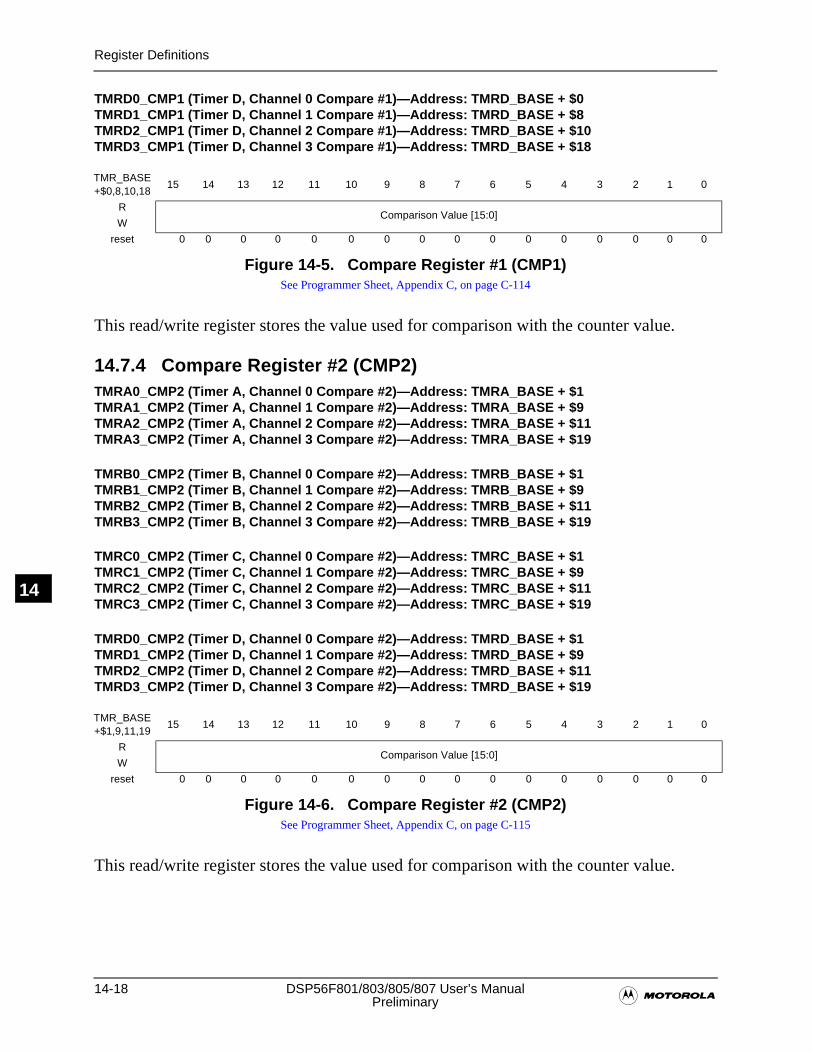
14-18 DSP56F801/803/805/807 User’s Manual�Preliminary
Register Definitions
14
TMRD0_CMP1 (Timer D, Channel 0 Compare #1)—Address: TMRD_BASE + $0TMRD1_CMP1 (Timer D, Channel 1 Compare #1)—Address: TMRD_BASE + $8TMRD2_CMP1 (Timer D, Channel 2 Compare #1)—Address: TMRD_BASE + $10TMRD3_CMP1 (Timer D, Channel 3 Compare #1)—Address: TMRD_BASE + $18
Figure 14-5. Compare Register #1 (CMP1)See Programmer Sheet, Appendix C, on page C-114
This read/write register stores the value used for comparison with the counter value.
14.7.4 Compare Register #2 (CMP2)TMRA0_CMP2 (Timer A, Channel 0 Compare #2)—Address: TMRA_BASE + $1TMRA1_CMP2 (Timer A, Channel 1 Compare #2)—Address: TMRA_BASE + $9TMRA2_CMP2 (Timer A, Channel 2 Compare #2)—Address: TMRA_BASE + $11TMRA3_CMP2 (Timer A, Channel 3 Compare #2)—Address: TMRA_BASE + $19
TMRB0_CMP2 (Timer B, Channel 0 Compare #2)—Address: TMRB_BASE + $1TMRB1_CMP2 (Timer B, Channel 1 Compare #2)—Address: TMRB_BASE + $9TMRB2_CMP2 (Timer B, Channel 2 Compare #2)—Address: TMRB_BASE + $11TMRB3_CMP2 (Timer B, Channel 3 Compare #2)—Address: TMRB_BASE + $19
TMRC0_CMP2 (Timer C, Channel 0 Compare #2)—Address: TMRC_BASE + $1TMRC1_CMP2 (Timer C, Channel 1 Compare #2)—Address: TMRC_BASE + $9TMRC2_CMP2 (Timer C, Channel 2 Compare #2)—Address: TMRC_BASE + $11TMRC3_CMP2 (Timer C, Channel 3 Compare #2)—Address: TMRC_BASE + $19
TMRD0_CMP2 (Timer D, Channel 0 Compare #2)—Address: TMRD_BASE + $1TMRD1_CMP2 (Timer D, Channel 1 Compare #2)—Address: TMRD_BASE + $9TMRD2_CMP2 (Timer D, Channel 2 Compare #2)—Address: TMRD_BASE + $11TMRD3_CMP2 (Timer D, Channel 3 Compare #2)—Address: TMRD_BASE + $19
Figure 14-6. Compare Register #2 (CMP2)See Programmer Sheet, Appendix C, on page C-115
This read/write register stores the value used for comparison with the counter value.
TMR_BASE+$0,8,10,18
15 14 13 12 11 10 9 8 7 6 5 4 3 2 1 0
RComparison Value [15:0]
W
reset 0 0 0 0 0 0 0 0 0 0 0 0 0 0 0 0
TMR_BASE+$1,9,11,19
15 14 13 12 11 10 9 8 7 6 5 4 3 2 1 0
RComparison Value [15:0]
W
reset 0 0 0 0 0 0 0 0 0 0 0 0 0 0 0 0
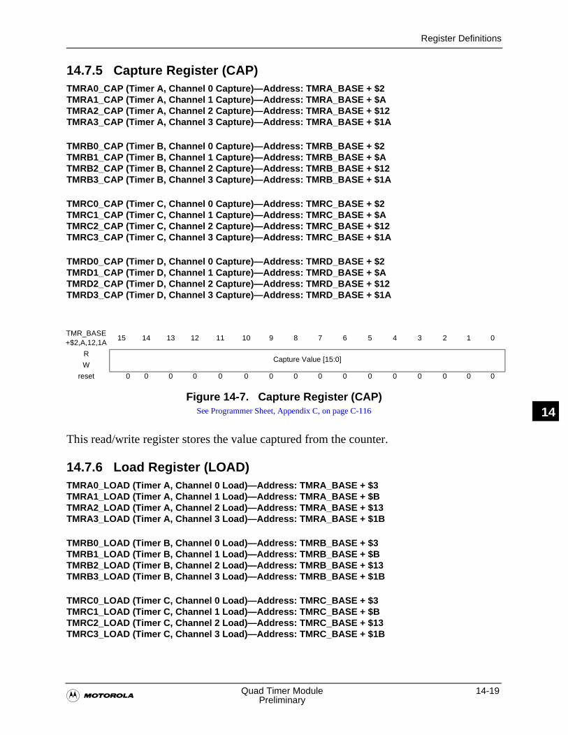
Register Definitions
�Quad Timer Module 14-19
Preliminary
14
14.7.5 Capture Register (CAP)TMRA0_CAP (Timer A, Channel 0 Capture)—Address: TMRA_BASE + $2TMRA1_CAP (Timer A, Channel 1 Capture)—Address: TMRA_BASE + $ATMRA2_CAP (Timer A, Channel 2 Capture)—Address: TMRA_BASE + $12TMRA3_CAP (Timer A, Channel 3 Capture)—Address: TMRA_BASE + $1A
TMRB0_CAP (Timer B, Channel 0 Capture)—Address: TMRB_BASE + $2TMRB1_CAP (Timer B, Channel 1 Capture)—Address: TMRB_BASE + $ATMRB2_CAP (Timer B, Channel 2 Capture)—Address: TMRB_BASE + $12TMRB3_CAP (Timer B, Channel 3 Capture)—Address: TMRB_BASE + $1A
TMRC0_CAP (Timer C, Channel 0 Capture)—Address: TMRC_BASE + $2TMRC1_CAP (Timer C, Channel 1 Capture)—Address: TMRC_BASE + $ATMRC2_CAP (Timer C, Channel 2 Capture)—Address: TMRC_BASE + $12TMRC3_CAP (Timer C, Channel 3 Capture)—Address: TMRC_BASE + $1A
TMRD0_CAP (Timer D, Channel 0 Capture)—Address: TMRD_BASE + $2TMRD1_CAP (Timer D, Channel 1 Capture)—Address: TMRD_BASE + $ATMRD2_CAP (Timer D, Channel 2 Capture)—Address: TMRD_BASE + $12TMRD3_CAP (Timer D, Channel 3 Capture)—Address: TMRD_BASE + $1A
Figure 14-7. Capture Register (CAP)See Programmer Sheet, Appendix C, on page C-116
This read/write register stores the value captured from the counter.
14.7.6 Load Register (LOAD)TMRA0_LOAD (Timer A, Channel 0 Load)—Address: TMRA_BASE + $3TMRA1_LOAD (Timer A, Channel 1 Load)—Address: TMRA_BASE + $BTMRA2_LOAD (Timer A, Channel 2 Load)—Address: TMRA_BASE + $13TMRA3_LOAD (Timer A, Channel 3 Load)—Address: TMRA_BASE + $1B
TMRB0_LOAD (Timer B, Channel 0 Load)—Address: TMRB_BASE + $3TMRB1_LOAD (Timer B, Channel 1 Load)—Address: TMRB_BASE + $BTMRB2_LOAD (Timer B, Channel 2 Load)—Address: TMRB_BASE + $13TMRB3_LOAD (Timer B, Channel 3 Load)—Address: TMRB_BASE + $1B
TMRC0_LOAD (Timer C, Channel 0 Load)—Address: TMRC_BASE + $3TMRC1_LOAD (Timer C, Channel 1 Load)—Address: TMRC_BASE + $BTMRC2_LOAD (Timer C, Channel 2 Load)—Address: TMRC_BASE + $13TMRC3_LOAD (Timer C, Channel 3 Load)—Address: TMRC_BASE + $1B
TMR_BASE+$2,A,12,1A
15 14 13 12 11 10 9 8 7 6 5 4 3 2 1 0
RCapture Value [15:0]
W
reset 0 0 0 0 0 0 0 0 0 0 0 0 0 0 0 0
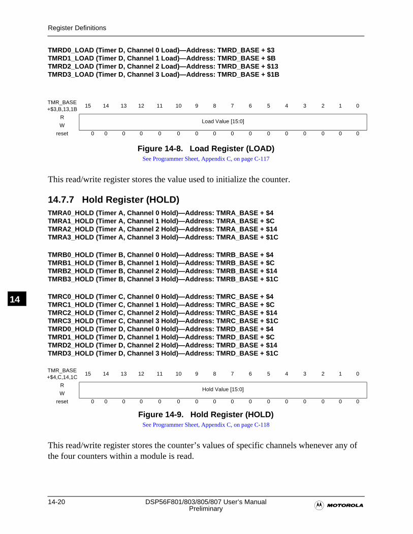
14-20 DSP56F801/803/805/807 User’s Manual�Preliminary
Register Definitions
14
TMRD0_LOAD (Timer D, Channel 0 Load)—Address: TMRD_BASE + $3TMRD1_LOAD (Timer D, Channel 1 Load)—Address: TMRD_BASE + $BTMRD2_LOAD (Timer D, Channel 2 Load)—Address: TMRD_BASE + $13TMRD3_LOAD (Timer D, Channel 3 Load)—Address: TMRD_BASE + $1B
Figure 14-8. Load Register (LOAD)See Programmer Sheet, Appendix C, on page C-117
This read/write register stores the value used to initialize the counter.
14.7.7 Hold Register (HOLD)TMRA0_HOLD (Timer A, Channel 0 Hold)—Address: TMRA_BASE + $4TMRA1_HOLD (Timer A, Channel 1 Hold)—Address: TMRA_BASE + $CTMRA2_HOLD (Timer A, Channel 2 Hold)—Address: TMRA_BASE + $14TMRA3_HOLD (Timer A, Channel 3 Hold)—Address: TMRA_BASE + $1C
TMRB0_HOLD (Timer B, Channel 0 Hold)—Address: TMRB_BASE + $4TMRB1_HOLD (Timer B, Channel 1 Hold)—Address: TMRB_BASE + $CTMRB2_HOLD (Timer B, Channel 2 Hold)—Address: TMRB_BASE + $14TMRB3_HOLD (Timer B, Channel 3 Hold)—Address: TMRB_BASE + $1C
TMRC0_HOLD (Timer C, Channel 0 Hold)—Address: TMRC_BASE + $4TMRC1_HOLD (Timer C, Channel 1 Hold)—Address: TMRC_BASE + $CTMRC2_HOLD (Timer C, Channel 2 Hold)—Address: TMRC_BASE + $14TMRC3_HOLD (Timer C, Channel 3 Hold)—Address: TMRC_BASE + $1CTMRD0_HOLD (Timer D, Channel 0 Hold)—Address: TMRD_BASE + $4TMRD1_HOLD (Timer D, Channel 1 Hold)—Address: TMRD_BASE + $CTMRD2_HOLD (Timer D, Channel 2 Hold)—Address: TMRD_BASE + $14TMRD3_HOLD (Timer D, Channel 3 Hold)—Address: TMRD_BASE + $1C
Figure 14-9. Hold Register (HOLD)See Programmer Sheet, Appendix C, on page C-118
This read/write register stores the counter’s values of specific channels whenever any of the four counters within a module is read.
TMR_BASE+$3,B,13,1B
15 14 13 12 11 10 9 8 7 6 5 4 3 2 1 0
RLoad Value [15:0]
W
reset 0 0 0 0 0 0 0 0 0 0 0 0 0 0 0 0
TMR_BASE+$4,C,14,1C
15 14 13 12 11 10 9 8 7 6 5 4 3 2 1 0
RHold Value [15:0]
W
reset 0 0 0 0 0 0 0 0 0 0 0 0 0 0 0 0
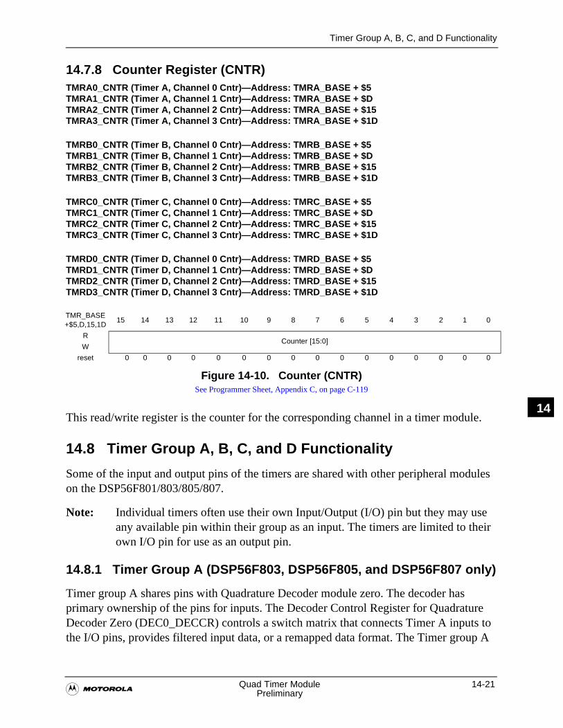
Timer Group A, B, C, and D Functionality
�Quad Timer Module 14-21
Preliminary
14
14.7.8 Counter Register (CNTR)TMRA0_CNTR (Timer A, Channel 0 Cntr)—Address: TMRA_BASE + $5TMRA1_CNTR (Timer A, Channel 1 Cntr)—Address: TMRA_BASE + $DTMRA2_CNTR (Timer A, Channel 2 Cntr)—Address: TMRA_BASE + $15TMRA3_CNTR (Timer A, Channel 3 Cntr)—Address: TMRA_BASE + $1D
TMRB0_CNTR (Timer B, Channel 0 Cntr)—Address: TMRB_BASE + $5TMRB1_CNTR (Timer B, Channel 1 Cntr)—Address: TMRB_BASE + $DTMRB2_CNTR (Timer B, Channel 2 Cntr)—Address: TMRB_BASE + $15TMRB3_CNTR (Timer B, Channel 3 Cntr)—Address: TMRB_BASE + $1D
TMRC0_CNTR (Timer C, Channel 0 Cntr)—Address: TMRC_BASE + $5TMRC1_CNTR (Timer C, Channel 1 Cntr)—Address: TMRC_BASE + $DTMRC2_CNTR (Timer C, Channel 2 Cntr)—Address: TMRC_BASE + $15TMRC3_CNTR (Timer C, Channel 3 Cntr)—Address: TMRC_BASE + $1D
TMRD0_CNTR (Timer D, Channel 0 Cntr)—Address: TMRD_BASE + $5TMRD1_CNTR (Timer D, Channel 1 Cntr)—Address: TMRD_BASE + $DTMRD2_CNTR (Timer D, Channel 2 Cntr)—Address: TMRD_BASE + $15TMRD3_CNTR (Timer D, Channel 3 Cntr)—Address: TMRD_BASE + $1D
Figure 14-10. Counter (CNTR)See Programmer Sheet, Appendix C, on page C-119
This read/write register is the counter for the corresponding channel in a timer module.
14.8 Timer Group A, B, C, and D Functionality
Some of the input and output pins of the timers are shared with other peripheral modules on the DSP56F801/803/805/807.
Note: Individual timers often use their own Input/Output (I/O) pin but they may use any available pin within their group as an input. The timers are limited to their own I/O pin for use as an output pin.
14.8.1 Timer Group A (DSP56F803, DSP56F805, and DSP56F807 only)
Timer group A shares pins with Quadrature Decoder module zero. The decoder has primary ownership of the pins for inputs. The Decoder Control Register for Quadrature Decoder Zero (DEC0_DECCR) controls a switch matrix that connects Timer A inputs to the I/O pins, provides filtered input data, or a remapped data format. The Timer group A
TMR_BASE+$5,D,15,1D
15 14 13 12 11 10 9 8 7 6 5 4 3 2 1 0
RCounter [15:0]
W
reset 0 0 0 0 0 0 0 0 0 0 0 0 0 0 0 0
14-22 DSP56F801/803/805/807 User’s Manual�Preliminary
Timer Group A, B, C, and D Functionality
14
outputs are directly connected to the I/O pins. If a timer’s output is enabled, its output will drive the I/O pin. The decoder module does not use the I/O pins for outputs.
Note: The Quadrature Decoder Zero module contains a quadrature test signal generator that can be monitored by the timer module on the timer zero (PHASEA0) input and the timer one (PHASEB0) input.
Timer A, counter zero input/output pin is shared with Quadrature Decoder Zero PHASEA0 pin.
Timer A, counter one I/O pin is shared with Quadrature Decoder One PHASEB0 pin.
Timer A, counter two I/O pin is shared with Quadrature Decoder Zero INDEX0 pin.
Timer A, counter three I/O pin is shared with Quadrature Decoder Zero HOME0 pin.
14.8.2 Timer Group B (DSP56F805 and DSP56F807 only)
Timer group B shares pins with Decoder module one. The decoder has primary ownership of the pins for inputs. The Decoder Control Register for Quadrature Decoder One, QD1_DECCR, controls a switch matrix that connects Timer B inputs to the I/O pins, provides filtered input data, or a remapped data format. The Timer group B outputs are directly connected to the I/O pins. If a timer’s output is enabled, its output will drive the I/O pin. The decoder module does not use the I/O pins for outputs.
Note: The Quadrature Decoder one module contains a quadrature test signal generator can be monitored by the timer module on the timer zero (PHASEA0) input and the timer one (PHASEB0) input.
Timer B, counter zero I/O pin is shared with Quadrature Decoder One PHASE0 pin.
Timer B, counter one I/O pin is shared with Quadrature Decoder One PHASE1 pin.
Timer B, counter two I/O pin is shared with Quadrature Decoder One INDEX1 pin.
Timer B, counter three I/O pin is shared with Quadrature Decoder One HOME1 pin.
14.8.3 Timer Group C
14.8.3.1 DSP56F805 and DSP56F807 only• Timer group C counters zero and one have dedicated I/O pins
• Timer C, counter zero has its own dedicated input/output pin TC0
• Timer C, counter one has its own dedicated input/output pin TC1
Timer Group A, B, C, and D Functionality
�Quad Timer Module 14-23
Preliminary
14
14.8.3.2 DSP56F801, DSP56F803, DSP56F805, and DSP56F807
Timers two and three do not have dedicated I/O pins. They can accept inputs from the PWM modules, and their outputs are connected to the ADC modules.
Note: Timers two and three can use the input pins allocated to timers zero and one, and their outputs can be used by timers zero and one. The intended purpose of Timers two and three is to provide a user selectable delay, One-Shot Mode, between the PWM sync signal and the updating of the ADC values.
• Timer C, counter two input is connected to the PWM A Sync output
• Timer C, counter two output is connected to the ADC A Sync input
• Timer C, counter three input is connected to the PWM B Sync output
• Timer C, counter three output is connected to the ADC B Sync input
14.8.4 Timer Group D
Timer group D has its own dedicated I/O pins varying in number between the DSP56F801/803/805/807 configurations.
14.8.4.1 DSP56F801• Timer D, counter zero has its own dedicated input/output pin TD0
• Timer D, counter one has its own dedicated input/output pin TD1
• Timer D, counter two has its own dedicated input/output pin TD2
Note: For the DSP56F801, the Timer Group D pins are multiplexed with GPIO pins so TD0 is muxed to GPIO6, TD1 is muxed to GPIO7, TD2 is muxed to GPIO8. This allows for additional General Purpose I/O when the Quad Timer is not needed.
14.8.4.2 DSP56F803• Timer D, counter one has its own dedicated input/output pin TD1
• Timer D, counter two has its own dedicated input/output pin TD2
14.8.4.3 DSP56F805 and DSP56F807• Timer D, counter zero has its own dedicated input/output pin TD0
• Timer D, counter one has its own dedicated input/output pin TD1
• Timer D, counter two has its own dedicated input/output pin TD2
• Timer D, counter three has its own dedicated input/output pin TD3
14-24 DSP56F801/803/805/807 User’s Manual�Preliminary
Timer Group A, B, C, and D Functionality
14
14.8.4.4 General Input Behavior
Time inputs are sampled at the peripheral clock rate. There is a delay of one peripheral clock period before the input can affect the behavior of a counter. This is typical of synchronous counters systems. There is one exception to this statement: when the counter is gated.
�On-chip Clock Synthesis (OCCS) 15-1
Preliminary
15
Chapter 15On-chip Clock Synthesis (OCCS)

15-2 DSP56F801/803/805/807 User’s Manual�Preliminary
15
Pin Descriptions
�On-chip Clock Synthesis (OCCS) 15-3
Preliminary
15
15.1 Introduction
The On-chip Clock Synthesis (OCCS) allows product design using inexpensive 8MHz crystals to run the DSP56F 801/803/8095/807 at any user selectable multiple from one to 80Mhz.
All peripherals on the DSP56F 801/803/805/807, except the COP/Watchdog Timer, run off the IPBus Clock frequency, the chip operating frequency (ZCLK) divided by two. The maximum frequency of operation is 80 MHz correlating to a 40MHz IPBus Clock frequency.
15.2 Features
The On-chip Clock Synthesis (OCCS) module interfaces to the Oscillator and PLL and has an on-chip Prescaler. The OCCS Module features are as follows:
• 2-bit Prescaler
• 2-bit Postscaler
• Ability to power down the internal PLL
• Selectable PLL source clock
• Selectable system clock (ZCLK) from three sources
The clock generation module provides the programming interface for both the PLL and on and off-chip oscillators.
15.3 Pin Descriptions
15.3.1 Oscillator Inputs (XTAL, EXTAL)
The oscillator inputs can be used to connect an external crystal or to directly drive the chip with an external clock source, thus bypassing the internal oscillator circuit. Design considerations for the external Clock Mode of operation are discussed in Section 15.3.2.
15.3.2 External Crystal Design ConsiderationsEither an external crystal oscillator or an external frequency source can be used to providea reference clock to the DSP56F801.
15.3.2.1 Crystal Oscillator
The internal crystal oscillator circuit is designed to interface with a parallel-resonant crystal resonator in the frequency range, specified for the external crystal, is four to eight MHz. Figure 15-1 shows a typical crystal oscillator circuit. Follow the crystal supplier’s
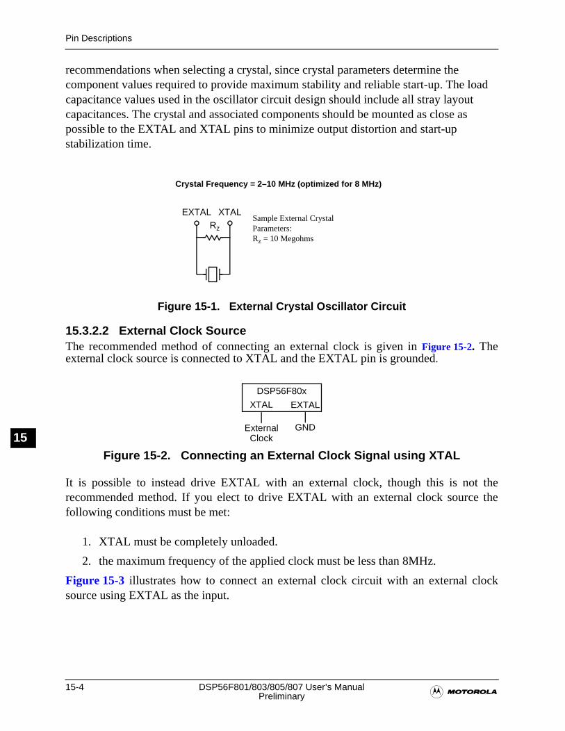
15-4 DSP56F801/803/805/807 User’s Manual�Preliminary
Pin Descriptions
15
recommendations when selecting a crystal, since crystal parameters determine the component values required to provide maximum stability and reliable start-up. The load capacitance values used in the oscillator circuit design should include all stray layout capacitances. The crystal and associated components should be mounted as close as possible to the EXTAL and XTAL pins to minimize output distortion and start-up stabilization time.
Figure 15-1. External Crystal Oscillator Circuit
15.3.2.2 External Clock SourceThe recommended method of connecting an external clock is given in Figure 15-2. Theexternal clock source is connected to XTAL and the EXTAL pin is grounded.
Figure 15-2. Connecting an External Clock Signal using XTAL
It is possible to instead drive EXTAL with an external clock, though this is not therecommended method. If you elect to drive EXTAL with an external clock source thefollowing conditions must be met:
1. XTAL must be completely unloaded.
2. the maximum frequency of the applied clock must be less than 8MHz.
Figure 15-3 illustrates how to connect an external clock circuit with an external clocksource using EXTAL as the input.
Sample External Crystal Parameters:Rz = 10 Megohms
Crystal Frequency = 2–10 MHz (optimized for 8 MHz)
EXTAL XTALRz
DSP56F80x
XTAL EXTAL
External GNDClock
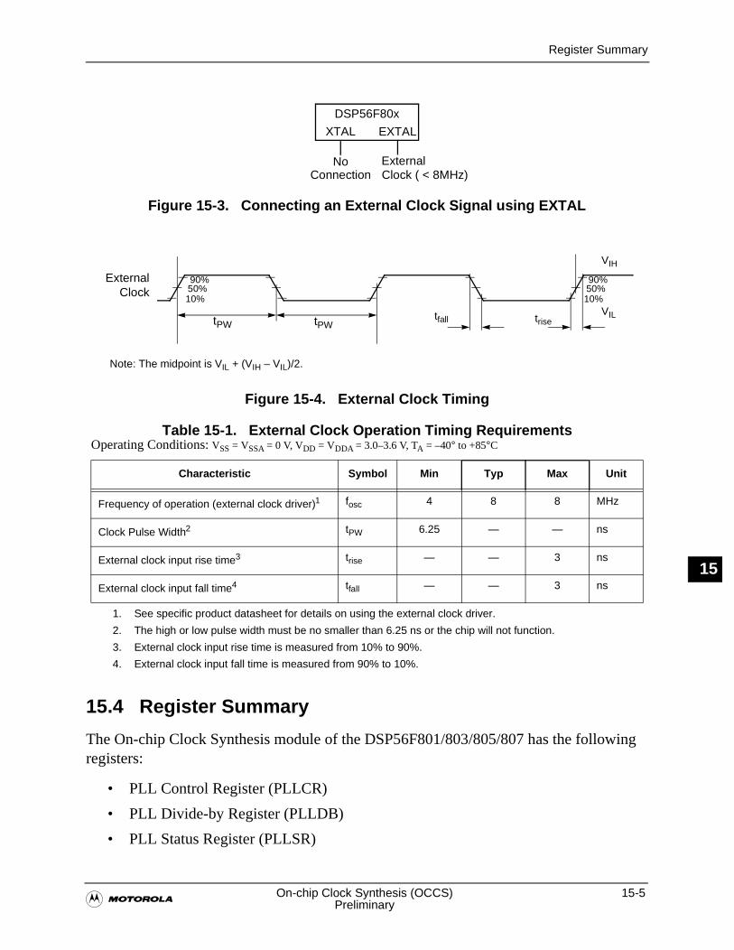
Register Summary
�On-chip Clock Synthesis (OCCS) 15-5
Preliminary
15
Figure 15-3. Connecting an External Clock Signal using EXTAL
Figure 15-4. External Clock Timing
Table 15-1. External Clock Operation Timing Requirements
15.4 Register Summary
The On-chip Clock Synthesis module of the DSP56F801/803/805/807 has the following registers:
• PLL Control Register (PLLCR)
• PLL Divide-by Register (PLLDB)
• PLL Status Register (PLLSR)
Operating Conditions: VSS = VSSA = 0 V, VDD = VDDA = 3.0–3.6 V, TA = –40° to +85°C
Characteristic Symbol Min Typ Max Unit
Frequency of operation (external clock driver)1
1. See specific product datasheet for details on using the external clock driver.
fosc 4 8 8 MHz
Clock Pulse Width2
2. The high or low pulse width must be no smaller than 6.25 ns or the chip will not function.
tPW 6.25 — — ns
External clock input rise time3
3. External clock input rise time is measured from 10% to 90%.
trise — — 3 ns
External clock input fall time4
4. External clock input fall time is measured from 90% to 10%.
tfall — — 3 ns
DSP56F80x
XTAL EXTAL
No ExternalConnection Clock ( < 8MHz)
ExternalClock
VIH
VIL
Note: The midpoint is VIL + (VIH – VIL)/2.
90%50%10%
90%50%10%
tPW tPWtfall trise
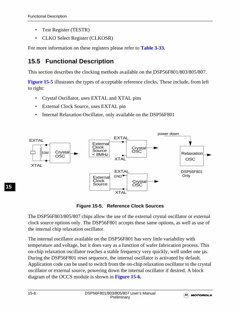
15-6 DSP56F801/803/805/807 User’s Manual�Preliminary
Functional Description
15
• Test Register (TESTR)
• CLKO Select Register (CLKOSR)
For more information on these registers please refer to Table 3-33.
15.5 Functional Description
This section describes the clocking methods available on the DSP56F801/803/805/807.
Figure 15-5 illustrates the types of acceptable reference clocks. These include, from left to right:
• Crystal Oscillator, uses EXTAL and XTAL pins
• External Clock Source, uses EXTAL pin
• Internal Relaxation Oscillator, only available on the DSP56F801
Figure 15-5. Reference Clock Sources
The DSP56F803/805/807 chips allow the use of the external crystal oscillator or external clock source options only. The DSP56F801 accepts these same options, as well as use of the internal chip relaxation oscillator.
The internal oscillator available on the DSP56F801 has very little variability with temperature and voltage, but it does vary as a function of wafer fabrication process. This on-chip relaxation oscillator reaches a stable frequency very quickly, well under one µs. During the DSP56F801 reset sequence, the internal oscillator is activated by default. Application code can be used to switch from the on-chip relaxation oscillator to the crystal oscillator or external source, powering down the internal oscillator if desired. A block diagram of the OCCS module is shown in Figure 15-6.
Crystal
EXTAL
XTAL
OSC10M
Crystal
EXTAL
XTAL
OSC
ExternalClockSource
OSC
Relaxation
power down
DSP56F801 Only
Crystal
EXTAL
XTAL
OSC
ExternalClockSource
GND
< 8MHz
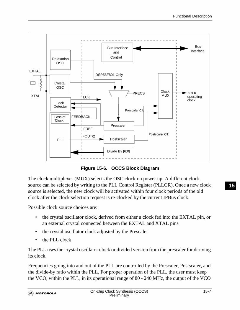
Functional Description
�On-chip Clock Synthesis (OCCS) 15-7
Preliminary
15
.
Figure 15-6. OCCS Block Diagram
The clock multiplexer (MUX) selects the OSC clock on power up. A different clock source can be selected by writing to the PLL Control Register (PLLCR). Once a new clock source is selected, the new clock will be activated within four clock periods of the old clock after the clock selection request is re-clocked by the current IPBus clock.
Possible clock source choices are:
• the crystal oscillator clock, derived from either a clock fed into the EXTAL pin, or an external crystal connected between the EXTAL and XTAL pins
• the crystal oscillator clock adjusted by the Prescaler
• the PLL clock
The PLL uses the crystal oscillator clock or divided version from the prescaler for deriving its clock.
Frequencies going into and out of the PLL are controlled by the Prescaler, Postscaler, and the divide-by ratio within the PLL. For proper operation of the PLL, the user must keep the VCO, within the PLL, in its operational range of 80 - 240 MHz, the output of the VCO
Crystal
Loss ofClock
PLL
Prescaler
Bus Interfaceand
Control
ClockMUX
Divide By [6:0]
ZCLK
BusInterface
EXTAL
XTAL
Postscaler
OSC
RelaxationOSC
DSP56F801 Only
LockDetector
FEEDBACK
FREF
LCK operatingclock
FOUT/2
Prescaler Clk
Postscaler Clk
PRECS
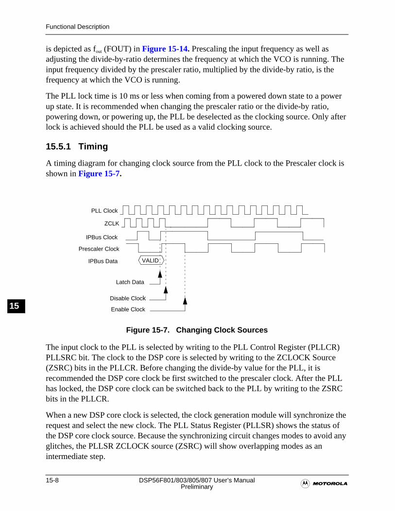
15-8 DSP56F801/803/805/807 User’s Manual�Preliminary
Functional Description
15
is depicted as fout (FOUT) in Figure 15-14. Prescaling the input frequency as well as adjusting the divide-by-ratio determines the frequency at which the VCO is running. The input frequency divided by the prescaler ratio, multiplied by the divide-by ratio, is the frequency at which the VCO is running.
The PLL lock time is 10 ms or less when coming from a powered down state to a power up state. It is recommended when changing the prescaler ratio or the divide-by ratio, powering down, or powering up, the PLL be deselected as the clocking source. Only after lock is achieved should the PLL be used as a valid clocking source.
15.5.1 Timing
A timing diagram for changing clock source from the PLL clock to the Prescaler clock is shown in Figure 15-7.
Figure 15-7. Changing Clock Sources
The input clock to the PLL is selected by writing to the PLL Control Register (PLLCR) PLLSRC bit. The clock to the DSP core is selected by writing to the ZCLOCK Source (ZSRC) bits in the PLLCR. Before changing the divide-by value for the PLL, it is recommended the DSP core clock be first switched to the prescaler clock. After the PLL has locked, the DSP core clock can be switched back to the PLL by writing to the ZSRC bits in the PLLCR.
When a new DSP core clock is selected, the clock generation module will synchronize the request and select the new clock. The PLL Status Register (PLLSR) shows the status of the DSP core clock source. Because the synchronizing circuit changes modes to avoid any glitches, the PLLSR ZCLOCK source (ZSRC) will show overlapping modes as an intermediate step.
ZCLK
VALIDIPBus Data
IPBus Clock
Prescaler Clock
PLL Clock
Latch Data
Disable Clock
Enable Clock
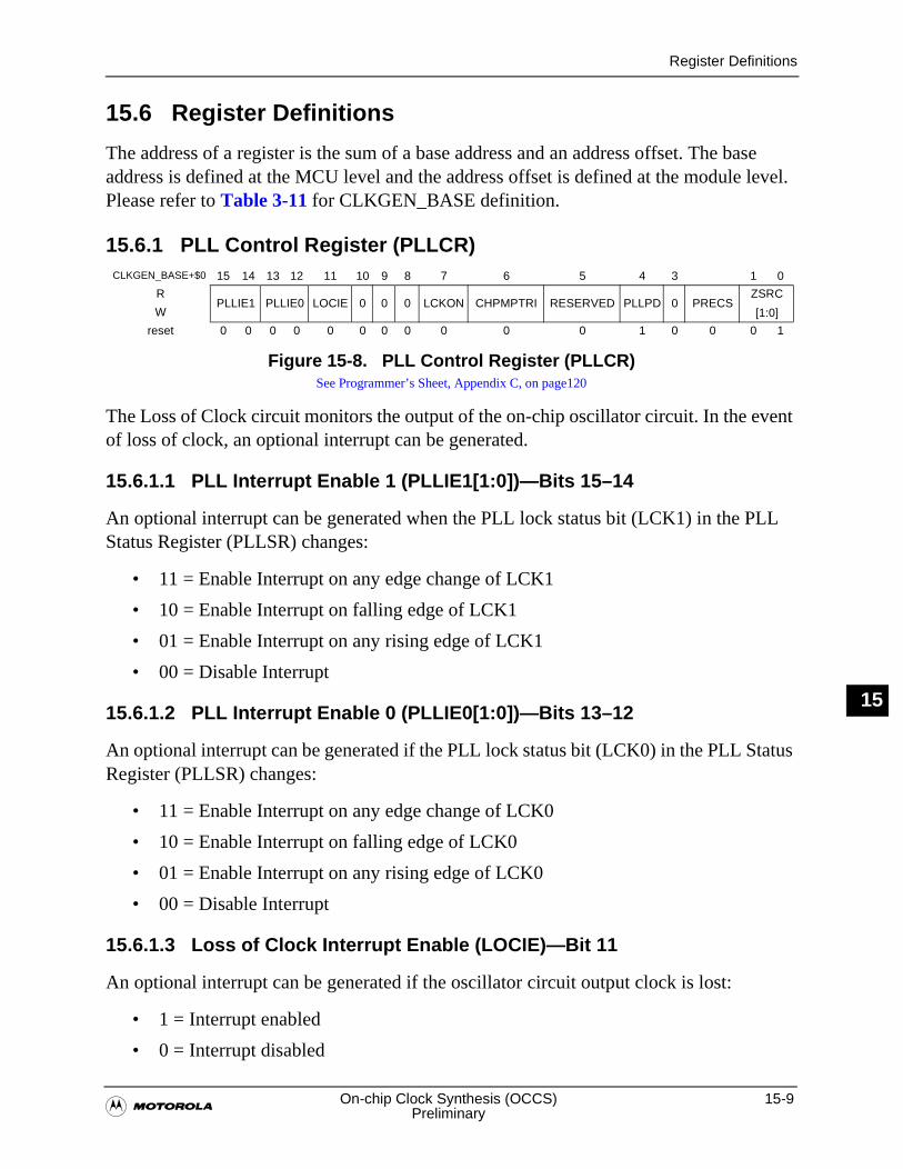
Register Definitions
�On-chip Clock Synthesis (OCCS) 15-9
Preliminary
15
15.6 Register Definitions
The address of a register is the sum of a base address and an address offset. The base address is defined at the MCU level and the address offset is defined at the module level. Please refer to Table 3-11 for CLKGEN_BASE definition.
15.6.1 PLL Control Register (PLLCR)
The Loss of Clock circuit monitors the output of the on-chip oscillator circuit. In the event of loss of clock, an optional interrupt can be generated.
15.6.1.1 PLL Interrupt Enable 1 (PLLIE1[1:0])—Bits 15–14
An optional interrupt can be generated when the PLL lock status bit (LCK1) in the PLL Status Register (PLLSR) changes:
• 11 = Enable Interrupt on any edge change of LCK1
• 10 = Enable Interrupt on falling edge of LCK1
• 01 = Enable Interrupt on any rising edge of LCK1
• 00 = Disable Interrupt
15.6.1.2 PLL Interrupt Enable 0 (PLLIE0[1:0])—Bits 13–12
An optional interrupt can be generated if the PLL lock status bit (LCK0) in the PLL Status Register (PLLSR) changes:
• 11 = Enable Interrupt on any edge change of LCK0
• 10 = Enable Interrupt on falling edge of LCK0
• 01 = Enable Interrupt on any rising edge of LCK0
• 00 = Disable Interrupt
15.6.1.3 Loss of Clock Interrupt Enable (LOCIE)—Bit 11
An optional interrupt can be generated if the oscillator circuit output clock is lost:
• 1 = Interrupt enabled
• 0 = Interrupt disabled
CLKGEN_BASE+$0 15 14 13 12 11 10 9 8 7 6 5 4 3 1 0
RPLLIE1 PLLIE0 LOCIE 0 0 0 LCKON CHPMPTRI RESERVED PLLPD 0 PRECS
ZSRC
[1:0]W
reset 0 0 0 0 0 0 0 0 0 0 0 1 0 0 0 1
Figure 15-8. PLL Control Register (PLLCR)See Programmer’s Sheet, Appendix C, on page120
15-10 DSP56F801/803/805/807 User’s Manual�Preliminary
Register Definitions
15
15.6.1.4 Reserved Bits—Bits 10–8
These reserved bits are read/write as zero, ensuring future compatibility.
15.6.1.5 Lock Detector On (LCKON)—Bit 7• 1 = Lock Detector enabled
• 0 = Lock Detector disabled
15.6.1.6 Charge Pump Tri-state (CHPMPTRI)—Bit 6
During normal chip operation the CHPMTRI bit should be set to a value of zero. In the event of Loss of Clock Reference the CHPMTRI bit must be set to a value of one. A value of one isolates the charge pump from the loop filter allowing the PLL output to slowly drift providing enough time to shut down the chip. Activating this bit will render the PLL inoperable and should not be done during standard operation of the chip.
Additionally, this bit is used for isolating the charge pump from the loop filter so the filter voltage can be driven from an external source during bench test evaluations.
15.6.1.7 Reserved Bit—Bit 5
This is a reserved bit and cannot be modified. It is read as zero.
15.6.1.8 PLL Power Down (PLLPD)—Bit 4
The PLL can be turned off by setting the PLLPD bit. There is a four IPBus Clock delay from changing the bit to signaling the PLL. When the PLL is powered down, the gear shifting logic automatically switches to ZSRC[2:0] = 001b in order to prevent loss of clock to the core.
• 1 = PLL powered down
• 0 = PLL enabled
15.6.1.9 Reserved Bit---Bit-3
This is a reserved bit and cannot be modified. It is read as zero.
15.6.1.10 Prescaler Clock Select (PRECS)—Bit 2
This bit is RESERVED (value 0) for the 803, 805 and 807. The following description is applicable to the 801:
This bit will not be allowed to be set unless the crystal oscillator is enabled in the GPIO. The clock source to the Prescaler can be selected to be either the Internal Relaxation Oscillator or the Crystal Oscillator
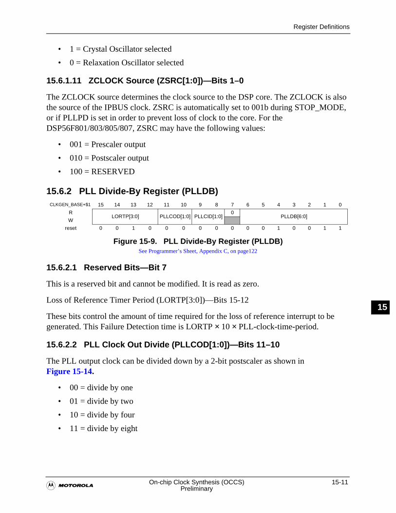
Register Definitions
�On-chip Clock Synthesis (OCCS) 15-11
Preliminary
15
• 1 = Crystal Oscillator selected
• 0 = Relaxation Oscillator selected
15.6.1.11 ZCLOCK Source (ZSRC[1:0])—Bits 1–0
The ZCLOCK source determines the clock source to the DSP core. The ZCLOCK is also the source of the IPBUS clock. ZSRC is automatically set to 001b during STOP_MODE, or if PLLPD is set in order to prevent loss of clock to the core. For the DSP56F801/803/805/807, ZSRC may have the following values:
• 001 = Prescaler output
• 010 = Postscaler output
• 100 = RESERVED
15.6.2 PLL Divide-By Register (PLLDB)
15.6.2.1 Reserved Bits—Bit 7
This is a reserved bit and cannot be modified. It is read as zero.
Loss of Reference Timer Period (LORTP[3:0])—Bits 15-12
These bits control the amount of time required for the loss of reference interrupt to be generated. This Failure Detection time is LORTP × 10 × PLL-clock-time-period.
15.6.2.2 PLL Clock Out Divide (PLLCOD[1:0])—Bits 11–10
The PLL output clock can be divided down by a 2-bit postscaler as shown in Figure 15-14.
• 00 = divide by one
• 01 = divide by two
• 10 = divide by four
• 11 = divide by eight
CLKGEN_BASE+$1 15 14 13 12 11 10 9 8 7 6 5 4 3 2 1 0
RLORTP[3:0] PLLCOD[1:0] PLLCID[1:0]
0PLLDB[6:0]
W
reset 0 0 1 0 0 0 0 0 0 0 0 1 0 0 1 1
Figure 15-9. PLL Divide-By Register (PLLDB)See Programmer’s Sheet, Appendix C, on page122
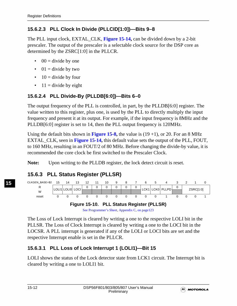
15-12 DSP56F801/803/805/807 User’s Manual�Preliminary
Register Definitions
15
15.6.2.3 PLL Clock In Divide (PLLCID[1:0])—Bits 9–8
The PLL input clock, EXTAL_CLK, Figure 15-14, can be divided down by a 2-bit prescaler. The output of the prescaler is a selectable clock source for the DSP core as determined by the ZSRC[1:0] in the PLLCR.
• 00 = divide by one
• 01 = divide by two
• 10 = divide by four
• 11 = divide by eight
15.6.2.4 PLL Divide-By (PLLDB[6:0])—Bits 6–0
The output frequency of the PLL is controlled, in part, by the PLLDB[6:0] register. The value written to this register, plus one, is used by the PLL to directly multiply the input frequency and present it at its output. For example, if the input frequency is 8MHz and the PLLDB[6:0] register is set to 14, then the PLL output frequency is 120MHz.
Using the default bits shown in Figure 15-8, the value is (19 +1), or 20. For an 8 MHz EXTAL_CLK, seen in Figure 15-14, this default value sets the output of the PLL, FOUT, to 160 MHz, resulting in an FOUT/2 of 80 MHz. Before changing the divide-by value, it is recommended the core clock be first switched to the Prescaler Clock.
Note: Upon writing to the PLLDB register, the lock detect circuit is reset.
15.6.3 PLL Status Register (PLLSR)
The Loss of Lock Interrupt is cleared by writing a one to the respective LOLI bit in the PLLSR. The Loss of Clock Interrupt is cleared by writing a one to the LOCI bit in the LOCSR. A PLL interrupt is generated if any of the LOLI or LOCI bits are set and the respective Interrupt enable is set in the PLLCR.
15.6.3.1 PLL Loss of Lock Interrupt 1 (LOLI1)—Bit 15
LOLI shows the status of the Lock detector state from LCK1 circuit. The Interrupt bit is cleared by writing a one to LOLI1 bit.
CLKGEN_BASE+$2 15 14 13 12 11 10 9 8 7 6 5 4 3 2 1 0
RLOLI1 LOLI0 LOCI
0 0 0 0 0 0LCK1 LCK0 PLLPD
0ZSRC[1:0]
W
reset 0 0 0 0 0 0 0 0 0 0 0 1 0 0 0 1
Figure 15-10. PLL Status Register (PLLSR)See Programmer’s Sheet, Appendix C, on page123
Register Definitions
�On-chip Clock Synthesis (OCCS) 15-13
Preliminary
15
• 1 = PLL not locked
• 0 = PLL locked
15.6.3.2 PLL Loss of Lock Interrupt 0 (LOLI0)—Bit 14
LOLI shows the status of the Lock detector state from LCK0 circuit. The Interrupt bit is cleared by writing a one to LOLI0 bit.
• 1 = PLL not locked
• 0 = PLL locked
15.6.3.3 Loss of Clock (LOCI)—Bit 13• 1 = Lost oscillator clock
• 0 = Oscillator clock normal
15.6.3.4 Reserved Bits—Bits 12–7 and 3
These reserved bits cannot be modified. They are read as zero.
15.6.3.5 Loss of Lock 1 (LCK1)—Bit 6• 1 = PLL is locked (coarse)
• 0 = PLL is unlocked (coarse)
15.6.3.6 Loss of Lock 0 (LCK0)—Bit 5• 1 = PLL is locked (fine)
• 0 = PLL is unlocked (fine)
15.6.3.7 PLL Power Down (PLLPDN)—Bit 4
PLL power down status is delayed by four IPBus Clocks from the PLLPD bit in the PLLCR.
• 1 = PLL powered down
• 0 = PLL not powered down
15.6.3.8 ZCLOCK Source (ZSRC[2:0])—Bits 2-0
ZSRC indicates the current ZCLOCK source. Since the synchronizing circuit switches the ZCLOCK source, ZSRC takes more than one IPBUS clock to indicate the new selection.
• 00 = Synchronizing in progress
• 01 = Prescaler output
• 10 = Postscaler output
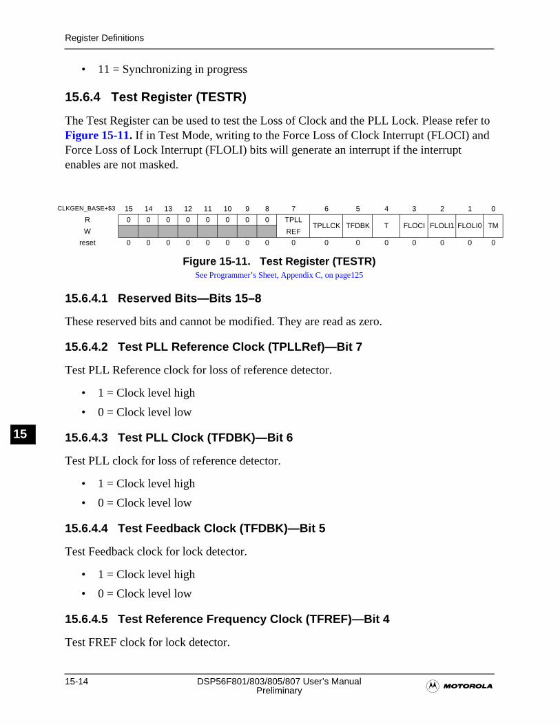
15-14 DSP56F801/803/805/807 User’s Manual�Preliminary
Register Definitions
15
• 11 = Synchronizing in progress
15.6.4 Test Register (TESTR)
The Test Register can be used to test the Loss of Clock and the PLL Lock. Please refer to Figure 15-11. If in Test Mode, writing to the Force Loss of Clock Interrupt (FLOCI) and Force Loss of Lock Interrupt (FLOLI) bits will generate an interrupt if the interrupt enables are not masked.
15.6.4.1 Reserved Bits—Bits 15–8
These reserved bits and cannot be modified. They are read as zero.
15.6.4.2 Test PLL Reference Clock (TPLLRef)—Bit 7
Test PLL Reference clock for loss of reference detector.
• 1 = Clock level high
• 0 = Clock level low
15.6.4.3 Test PLL Clock (TFDBK)—Bit 6
Test PLL clock for loss of reference detector.
• 1 = Clock level high
• 0 = Clock level low
15.6.4.4 Test Feedback Clock (TFDBK)—Bit 5
Test Feedback clock for lock detector.
• 1 = Clock level high
• 0 = Clock level low
15.6.4.5 Test Reference Frequency Clock (TFREF)—Bit 4
Test FREF clock for lock detector.
CLKGEN_BASE+$3 15 14 13 12 11 10 9 8 7 6 5 4 3 2 1 0
R 0 0 0 0 0 0 0 0 TPLL
REFTPLLCK TFDBK T FLOCI FLOLI1 FLOLI0 TM
W
reset 0 0 0 0 0 0 0 0 0 0 0 0 0 0 0 0
Figure 15-11. Test Register (TESTR)See Programmer’s Sheet, Appendix C, on page125
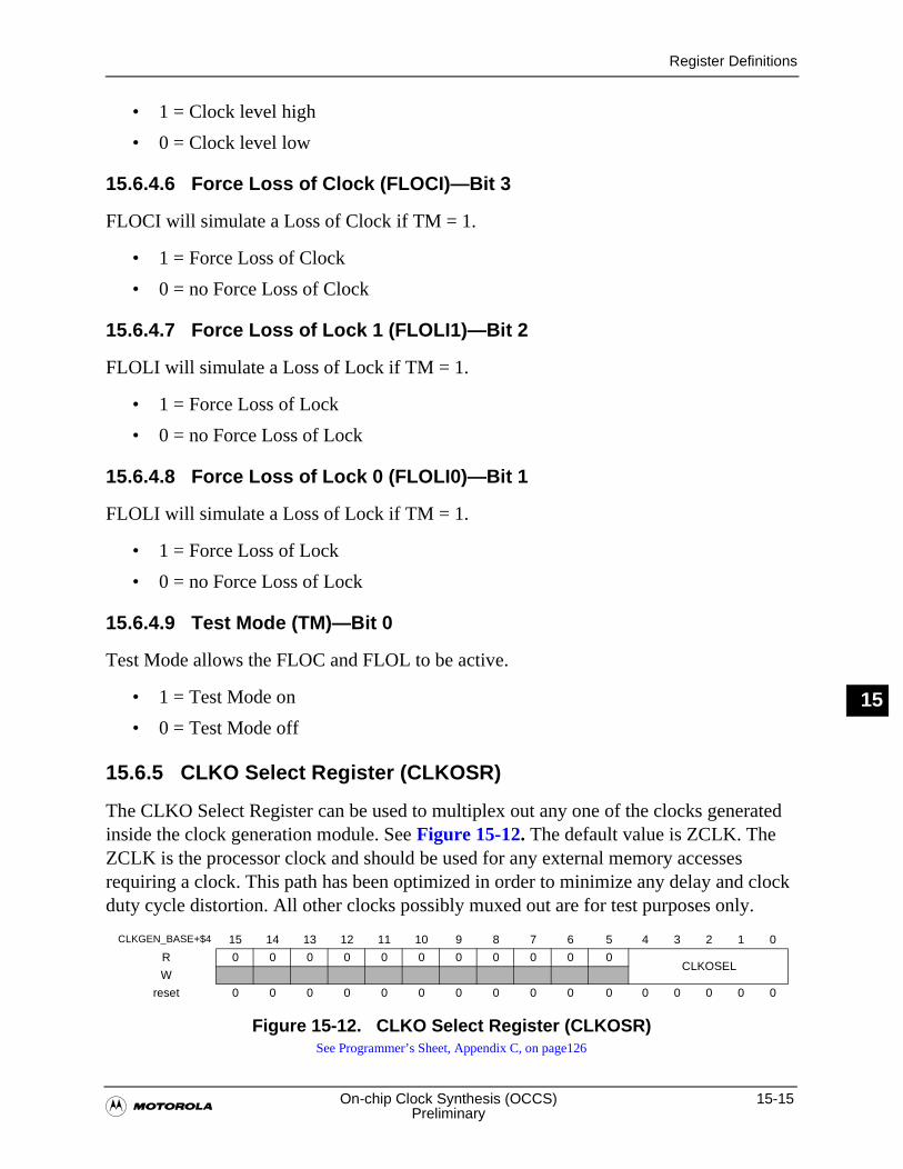
Register Definitions
�On-chip Clock Synthesis (OCCS) 15-15
Preliminary
15
• 1 = Clock level high
• 0 = Clock level low
15.6.4.6 Force Loss of Clock (FLOCI)—Bit 3
FLOCI will simulate a Loss of Clock if TM = 1.
• 1 = Force Loss of Clock
• 0 = no Force Loss of Clock
15.6.4.7 Force Loss of Lock 1 (FLOLI1)—Bit 2
FLOLI will simulate a Loss of Lock if TM = 1.
• 1 = Force Loss of Lock
• 0 = no Force Loss of Lock
15.6.4.8 Force Loss of Lock 0 (FLOLI0)—Bit 1
FLOLI will simulate a Loss of Lock if TM = 1.
• 1 = Force Loss of Lock
• 0 = no Force Loss of Lock
15.6.4.9 Test Mode (TM)—Bit 0
Test Mode allows the FLOC and FLOL to be active.
• 1 = Test Mode on
• 0 = Test Mode off
15.6.5 CLKO Select Register (CLKOSR)
The CLKO Select Register can be used to multiplex out any one of the clocks generated inside the clock generation module. See Figure 15-12. The default value is ZCLK. The ZCLK is the processor clock and should be used for any external memory accesses requiring a clock. This path has been optimized in order to minimize any delay and clock duty cycle distortion. All other clocks possibly muxed out are for test purposes only.
Figure 15-12. CLKO Select Register (CLKOSR)See Programmer’s Sheet, Appendix C, on page126
CLKGEN_BASE+$4 15 14 13 12 11 10 9 8 7 6 5 4 3 2 1 0
R 0 0 0 0 0 0 0 0 0 0 0CLKOSEL
W
reset 0 0 0 0 0 0 0 0 0 0 0 0 0 0 0 0
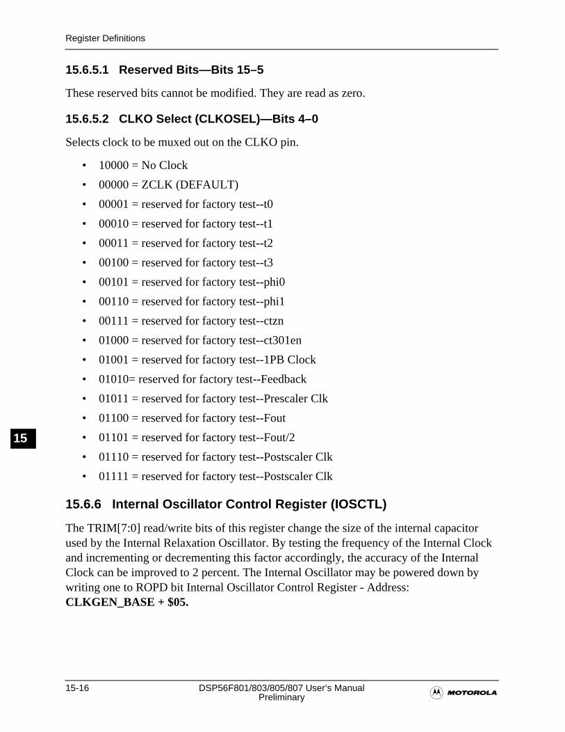
15-16 DSP56F801/803/805/807 User’s Manual�Preliminary
Register Definitions
15
15.6.5.1 Reserved Bits—Bits 15–5
These reserved bits cannot be modified. They are read as zero.
15.6.5.2 CLKO Select (CLKOSEL)—Bits 4–0
Selects clock to be muxed out on the CLKO pin.
• 10000 = No Clock
• 00000 = ZCLK (DEFAULT)
• 00001 = reserved for factory test--t0
• 00010 = reserved for factory test--t1
• 00011 = reserved for factory test--t2
• 00100 = reserved for factory test--t3
• 00101 = reserved for factory test--phi0
• 00110 = reserved for factory test--phi1
• 00111 = reserved for factory test--ctzn
• 01000 = reserved for factory test--ct301en
• 01001 = reserved for factory test--1PB Clock
• 01010= reserved for factory test--Feedback
• 01011 = reserved for factory test--Prescaler Clk
• 01100 = reserved for factory test--Fout
• 01101 = reserved for factory test--Fout/2
• 01110 = reserved for factory test--Postscaler Clk
• 01111 = reserved for factory test--Postscaler Clk
15.6.6 Internal Oscillator Control Register (IOSCTL)
The TRIM[7:0] read/write bits of this register change the size of the internal capacitor used by the Internal Relaxation Oscillator. By testing the frequency of the Internal Clock and incrementing or decrementing this factor accordingly, the accuracy of the Internal Clock can be improved to 2 percent. The Internal Oscillator may be powered down by writing one to ROPD bit Internal Oscillator Control Register - Address: CLKGEN_BASE + $05.
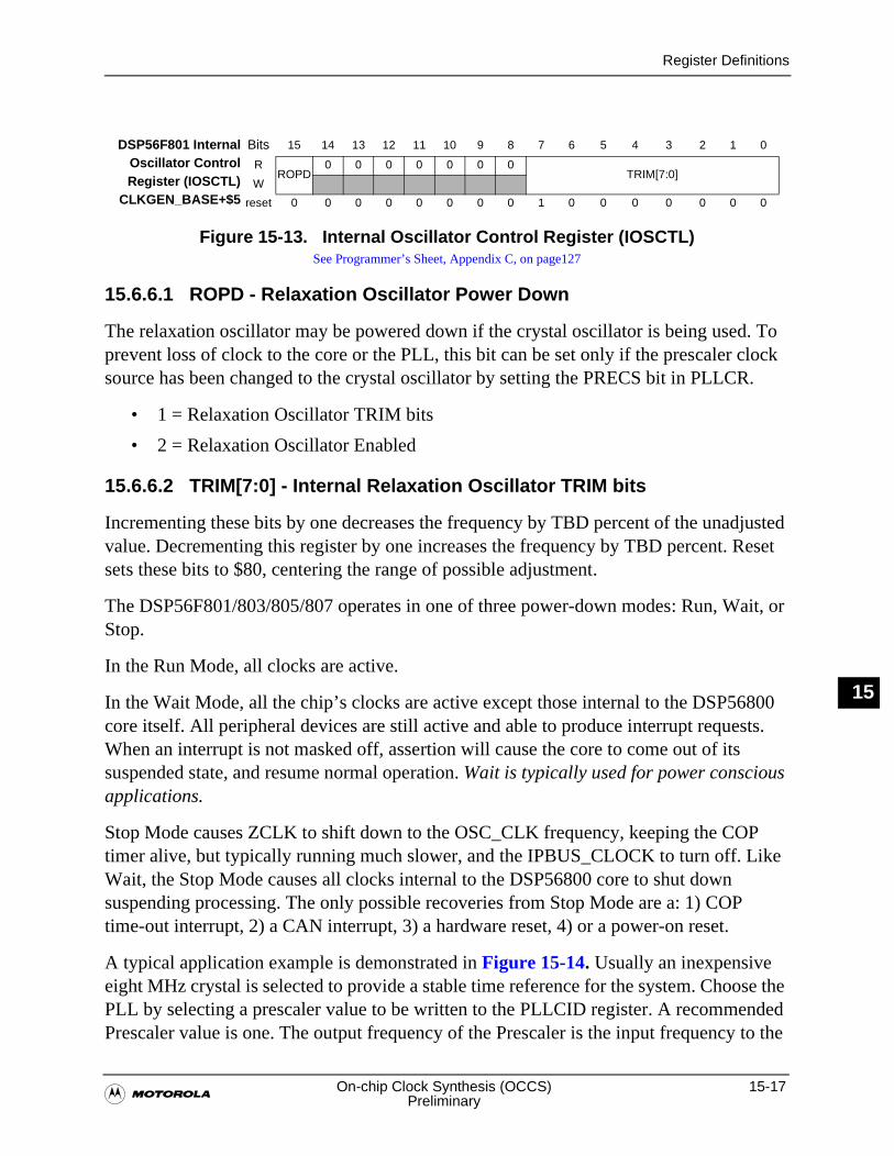
Register Definitions
�On-chip Clock Synthesis (OCCS) 15-17
Preliminary
15
Figure 15-13. Internal Oscillator Control Register (IOSCTL)See Programmer’s Sheet, Appendix C, on page127
15.6.6.1 ROPD - Relaxation Oscillator Power Down
The relaxation oscillator may be powered down if the crystal oscillator is being used. To prevent loss of clock to the core or the PLL, this bit can be set only if the prescaler clock source has been changed to the crystal oscillator by setting the PRECS bit in PLLCR.
• 1 = Relaxation Oscillator TRIM bits
• 2 = Relaxation Oscillator Enabled
15.6.6.2 TRIM[7:0] - Internal Relaxation Oscillator TRIM bits
Incrementing these bits by one decreases the frequency by TBD percent of the unadjusted value. Decrementing this register by one increases the frequency by TBD percent. Reset sets these bits to $80, centering the range of possible adjustment.
The DSP56F801/803/805/807 operates in one of three power-down modes: Run, Wait, or Stop.
In the Run Mode, all clocks are active.
In the Wait Mode, all the chip’s clocks are active except those internal to the DSP56800 core itself. All peripheral devices are still active and able to produce interrupt requests. When an interrupt is not masked off, assertion will cause the core to come out of its suspended state, and resume normal operation. Wait is typically used for power conscious applications.
Stop Mode causes ZCLK to shift down to the OSC_CLK frequency, keeping the COP timer alive, but typically running much slower, and the IPBUS_CLOCK to turn off. Like Wait, the Stop Mode causes all clocks internal to the DSP56800 core to shut down suspending processing. The only possible recoveries from Stop Mode are a: 1) COP time-out interrupt, 2) a CAN interrupt, 3) a hardware reset, 4) or a power-on reset.
A typical application example is demonstrated in Figure 15-14. Usually an inexpensive eight MHz crystal is selected to provide a stable time reference for the system. Choose the PLL by selecting a prescaler value to be written to the PLLCID register. A recommended Prescaler value is one. The output frequency of the Prescaler is the input frequency to the
DSP56F801 InternalOscillator ControlRegister (IOSCTL)
CLKGEN_BASE+$5
Bits 15 14 13 12 11 10 9 8 7 6 5 4 3 2 1 0
RROPD
0 0 0 0 0 0 0TRIM[7:0]
W
reset 0 0 0 0 0 0 0 0 1 0 0 0 0 0 0 0
15-18 DSP56F801/803/805/807 User’s Manual�Preliminary
Register Definitions
15
PLL. This frequency is multiplied written the PLL, by the value, plus one. The result is written to the PLLDB[6:0] register. The resulting frequency is depicted as FOUT in Figure 15-14. Divide the frequency by two through a fixed divider at the output of the PLL prior to being presented to the postscaler divider. The postscaler divider further apportions the frequency by its user-defined value before presenting it as ZCLK through the Sync Mux. Setting the frequency using the programmable divider is discussed in Section 15.6.2.4.
Figure 15-14. Relationship of IPBus Clock and ZCLK
Note: The maximum frequency of operation is 80 MHz correlating to a 40 MHz IPBus Clock frequency.
The CAN module can elect to use the OSC_CLOCK frequency directly for CAN applications requiring extraordinary jitter constraints, or for CAN operation during Stop Mode.
The following table summarizes the state of the on-chip clocks in typical operating frequencies during the various power-down modes.
Note: All peripherals, except the COP/Watchdog Timer, run off of the IPBus Clock.
Table 15-2. On-chip Clock States
State ZCLK IPBUS_CLK
Run 80 MHz 40 MHz
CrystalOsc.
Prescalerdiv. by 1,2,4,8
SyncMUX
COP
Loss of Clock
IRQ
Postscalerdiv. by 1,2,4,8
Loss of Lock
IRQ
SIM
56800
IP_Bus
Peripheral
CAN
DSPCore
Bridgediv.by 2
Peripheral
Peripheral
EXTAL
XTAL
OSC_CLOCK
IP_B
US
CLO
CK
40 M
Hz
Typ.
en
COPIRQ
ZC
LK, 8
0 M
Hz
Typ.
8 MHz Typ.
EXTAL_CLK
FOUT/2
(PLLCID bits)
(PLLCOD bits)VCO
PHCOMP
DIV
BY*DIV
BY 2
*Divided by (PLLDB + 1)
PLL
FOUT
Relaxation Osc. (801)
8MHz
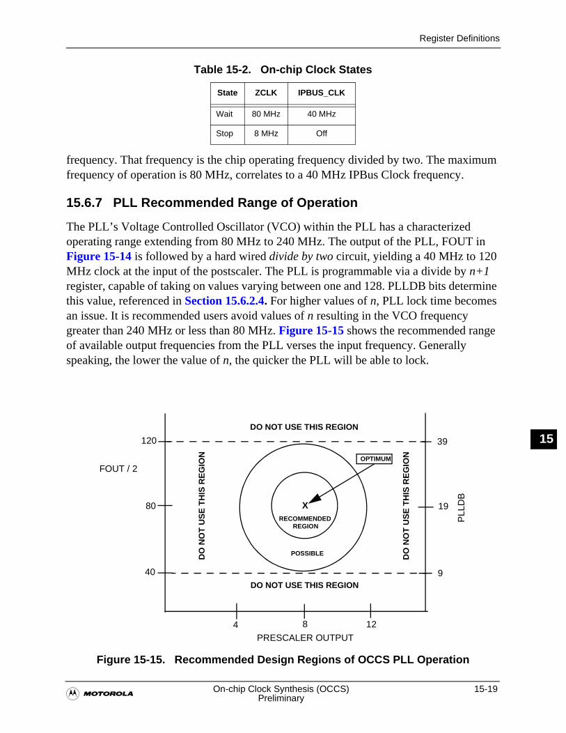
Register Definitions
�On-chip Clock Synthesis (OCCS) 15-19
Preliminary
15
frequency. That frequency is the chip operating frequency divided by two. The maximum frequency of operation is 80 MHz, correlates to a 40 MHz IPBus Clock frequency.
15.6.7 PLL Recommended Range of Operation
The PLL’s Voltage Controlled Oscillator (VCO) within the PLL has a characterized operating range extending from 80 MHz to 240 MHz. The output of the PLL, FOUT in Figure 15-14 is followed by a hard wired divide by two circuit, yielding a 40 MHz to 120 MHz clock at the input of the postscaler. The PLL is programmable via a divide by n+1 register, capable of taking on values varying between one and 128. PLLDB bits determine this value, referenced in Section 15.6.2.4. For higher values of n, PLL lock time becomes an issue. It is recommended users avoid values of n resulting in the VCO frequency greater than 240 MHz or less than 80 MHz. Figure 15-15 shows the recommended range of available output frequencies from the PLL verses the input frequency. Generally speaking, the lower the value of n, the quicker the PLL will be able to lock.
Figure 15-15. Recommended Design Regions of OCCS PLL Operation
Wait 80 MHz 40 MHz
Stop 8 MHz Off
Table 15-2. On-chip Clock States
State ZCLK IPBUS_CLK
PRESCALER OUTPUT
40
80
120
84 12
DO NOT USE THIS REGION
DO NOT USE THIS REGION
DO
NO
T U
SE
TH
IS R
EG
ION
DO
NO
T U
SE
TH
IS R
EG
ION
X
POSSIBLE
OPTIMUM
REGIONRECOMMENDED
39
19
9
PLL
DB
FOUT / 2
15-20 DSP56F801/803/805/807 User’s Manual�Preliminary
PLL Lock Time Specification
15
15.7 PLL Lock Time Specification
In many applications, the lock time of the PLL is the most critical PLL design parameters. Proper design and use of the PLL ensures the highest stability and lowest lock time.
15.7.1 Lock Time Definition
Typical control systems refer to the lock time as the reaction time within specified tolerances of the system to a step input. In a PLL, the step input occurs when the PLL is turned on or when it suffers a noise hit. The tolerance is usually specified as a percent of the step input or when the output settles to the desired value plus or minus a percent of the frequency change. Therefore, the reaction time is constant in this definition, regardless of the size of the step input.
When the PLL is coming from a powered down state, PLL_PDN high, to a powered up condition, PLL_PDN low, the maximum lock time, with a divide by count of 16 or less, is 10ms.
Other systems refer to lock time as the time the system takes to reduce the error between the actual output and the desired output to within specified tolerances. Therefore, the lock time varies according to the original error in the output. Minor errors may be shorter or longer in many cases.
15.7.2 Parametric Influences on Reaction Time
Lock time is designed to be as short as possible while still providing the highest possible stability. The reaction time is not constant, however. Many factors directly and indirectly affect the lock time.
The most critical parameter affecting the reaction time of the PLL is the reference frequency, FREF, illustrated in Figure 15-6. This frequency is the input to the phase detector and controls how often the PLL makes corrections. For stability, it is desirable for the corrections to be small and frequent. Therefore, a higher reference frequency provides optimal performance; 8MHz is preferred. This parameter is under user control through the choice of OSC_CLK frequency FOSC and the value programmed in the reference divider.
15.8 PLL Frequency Lock Detector Block
This digital block monitors the VCO output clock and sets the LCK[1:0] bits in the PLL Status Register (PLLSR) based on its frequency accuracy. The lock detector is enabled with the LCKON bit of the PLL Control Register (PLLCR), as well as the PLL_PDN bit of PLLCR. Once enabled, the detector starts two counters whose outputs are periodically compared. The input clocks to these counters are the VCO output clock divided by the value in the /N Register, called feedback, and the PLL input clock, shown as FREF in
PLL Frequency Lock Detector Block
�On-chip Clock Synthesis (OCCS) 15-21
Preliminary
15
Figure 15-6. The period of the pulses being compared cover one whole period of each clock. This is due to the feedback clock not guaranteeing a 50 percentage duty cycle. The design of this block was accomplished with the assumption the feedback clock transitions high on the rising edge of FREF.
Feedback and FREF clocks are compared after 16, 32, and 64 cycles. If, after 32 cycles, the clocks match, the LCK0 bit is set to one. If, after 64 cycles of FREF, there is the same number of FREF clocks as feedback clocks, the LCK1 bit is also set. The LCK bit stay set until:
• Clocks fail to match
• When a new value is written to the N-factor
• On reset caused by LCKON, PLL_PDN
• Chip_level reset
When the circuit sets the LCK1, the two counters are reset and start the count again. The lock detector is designed so if LCK1 is reset to zero because clocks did not match, LCK0 can stay high. This provides the processor the accuracy of the two clocks with respect to each other.
15-22 DSP56F801/803/805/807 User’s Manual�Preliminary
PLL Frequency Lock Detector Block
15
�Reset, Low Voltage, Stop and Wait Operation 16-1
Preliminary
IN16
Chapter 16Reset, Low Voltage, Stop and Wait
Operation

16-2 DSP56F801/803/805/807 User’s Manual�Preliminary
16
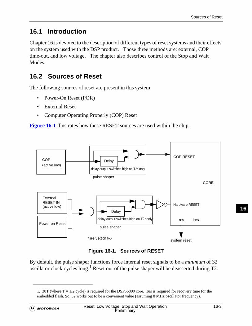
Sources of Reset
�Reset, Low Voltage, Stop and Wait Operation 16-3
Preliminary
IN16
16.1 Introduction
Chapter 16 is devoted to the description of different types of reset systems and their effects on the system used with the DSP product. Those three methods are: external, COP time-out, and low voltage. The chapter also describes control of the Stop and Wait Modes.
16.2 Sources of Reset
The following sources of reset are present in this system:
• Power-On Reset (POR)
• External Reset
• Computer Operating Properly (COP) Reset
Figure 16-1 illustrates how these RESET sources are used within the chip.
Figure 16-1. Sources of RESET
By default, the pulse shaper functions force internal reset signals to be a minimum of 32 oscillator clock cycles long.1 Reset out of the pulse shaper will be deasserted during T2.
1. 38T (where T = 1/2 cycle) is required for the DSP56800 core. 1us is required for recovery time for the embedded flash. So, 32 works out to be a convenient value (assuming 8 MHz oscillator frequency).
Hardware RESET
COP RESET
CORE
COP
ExternalRESET IN
res ires
Delay
delay output switches high on T2* only
pulse shaper
Delay
delay output switches high on T2 *only
pulse shaper
(active low)
(active low)
system reset
Power on Reset
*see Section 6-6
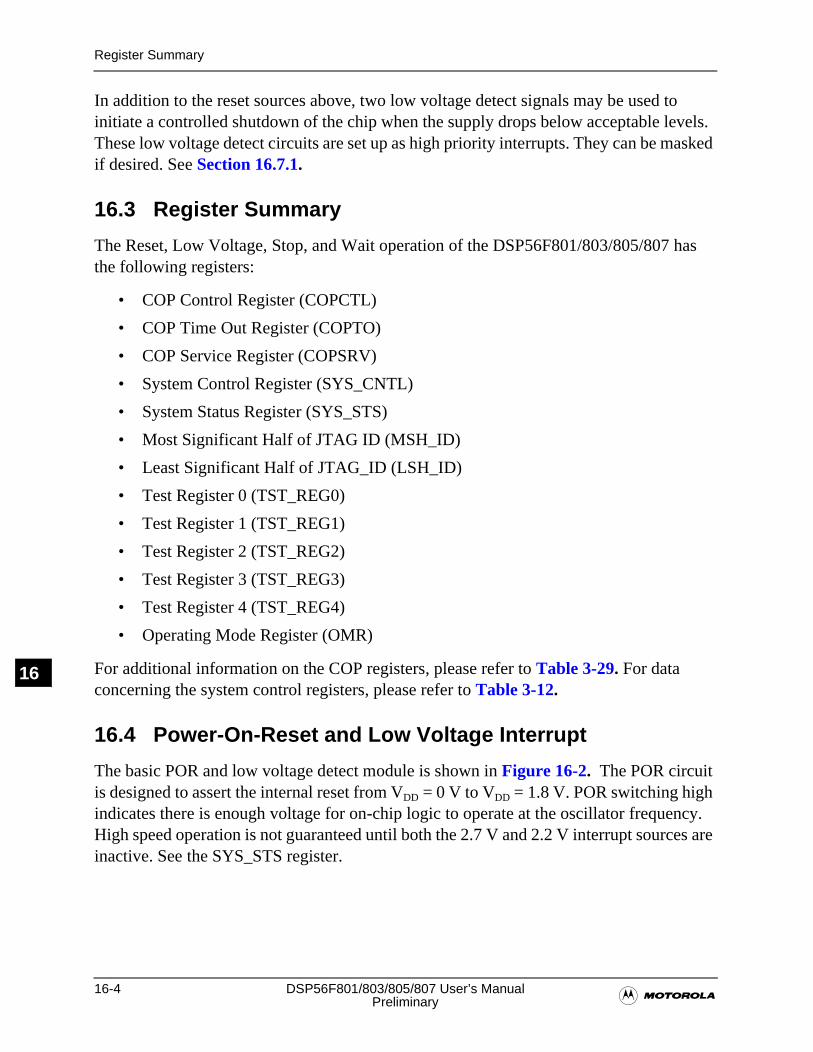
16-4 DSP56F801/803/805/807 User’s Manual�Preliminary
Register Summary
16
In addition to the reset sources above, two low voltage detect signals may be used to initiate a controlled shutdown of the chip when the supply drops below acceptable levels. These low voltage detect circuits are set up as high priority interrupts. They can be masked if desired. See Section 16.7.1.
16.3 Register Summary
The Reset, Low Voltage, Stop, and Wait operation of the DSP56F801/803/805/807 has the following registers:
• COP Control Register (COPCTL)
• COP Time Out Register (COPTO)
• COP Service Register (COPSRV)
• System Control Register (SYS_CNTL)
• System Status Register (SYS_STS)
• Most Significant Half of JTAG ID (MSH_ID)
• Least Significant Half of JTAG_ID (LSH_ID)
• Test Register 0 (TST_REG0)
• Test Register 1 (TST_REG1)
• Test Register 2 (TST_REG2)
• Test Register 3 (TST_REG3)
• Test Register 4 (TST_REG4)
• Operating Mode Register (OMR)
For additional information on the COP registers, please refer to Table 3-29. For data concerning the system control registers, please refer to Table 3-12.
16.4 Power-On-Reset and Low Voltage Interrupt
The basic POR and low voltage detect module is shown in Figure 16-2. The POR circuit is designed to assert the internal reset from VDD = 0 V to VDD = 1.8 V. POR switching high indicates there is enough voltage for on-chip logic to operate at the oscillator frequency. High speed operation is not guaranteed until both the 2.7 V and 2.2 V interrupt sources are inactive. See the SYS_STS register.
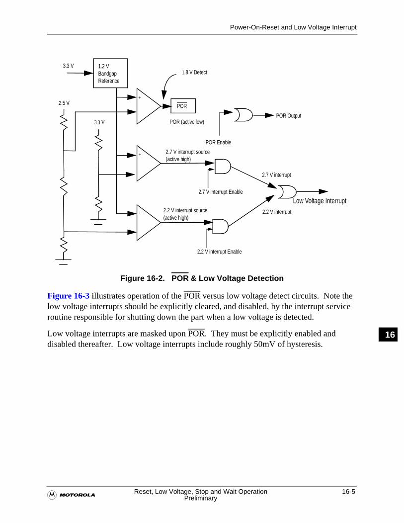
Power-On-Reset and Low Voltage Interrupt
�Reset, Low Voltage, Stop and Wait Operation 16-5
Preliminary
IN16
Figure 16-2. POR & Low Voltage Detection
Figure 16-3 illustrates operation of the POR versus low voltage detect circuits. Note the low voltage interrupts should be explicitly cleared, and disabled, by the interrupt service routine responsible for shutting down the part when a low voltage is detected.
Low voltage interrupts are masked upon POR. They must be explicitly enabled and disabled thereafter. Low voltage interrupts include roughly 50mV of hysteresis.
2.2 V interrupt Enable
1.2 VBandgapReference
3.3 V
3.3 V
2.5 V+
+
+
POR
POR (active low)
2.7 V interrupt source(active high)
2.2 V interrupt source(active high)
1.8 V Detect
POR Enable
POR Output
2.7 V interrupt Enable
2.7 V interrupt
2.2 V interrupt
Low Voltage Interrupt
16-6 DSP56F801/803/805/807 User’s Manual�Preliminary
External Reset
16
Figure 16-3. POR Versus Low-Voltage Interrupts
16.5 External Reset
The external reset is active low, and will cause the part to be immediately placed in a reset condition. Some internal portions of the chip may be synchronously reset. The internal waveform shaper ensures the internal reset remains low long enough for all portions of the chip to achieve their reset value.
When the RESET pin is withheld, the initial chip operating mode is latched into the OMR. OMR latching is based upon the value present on the EXTBOOT pin. Please refer to Section 3.3.2 for additional details.
32 Clock Cycles
VDD
Hashed levels show outputs from analog circuitry.
POR
Low-V Interrupt
Interrupt cleared by user software here
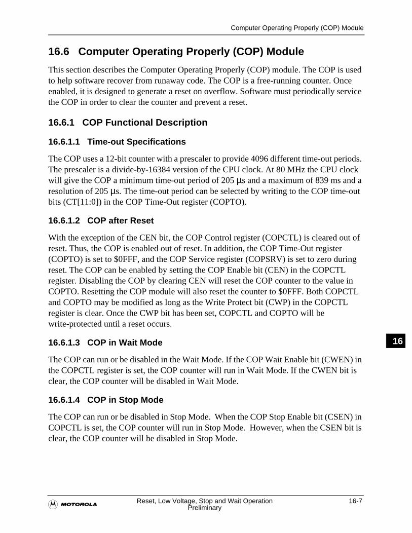
Computer Operating Properly (COP) Module
�Reset, Low Voltage, Stop and Wait Operation 16-7
Preliminary
IN16
16.6 Computer Operating Properly (COP) Module
This section describes the Computer Operating Properly (COP) module. The COP is used to help software recover from runaway code. The COP is a free-running counter. Once enabled, it is designed to generate a reset on overflow. Software must periodically service the COP in order to clear the counter and prevent a reset.
16.6.1 COP Functional Description
16.6.1.1 Time-out Specifications
The COP uses a 12-bit counter with a prescaler to provide 4096 different time-out periods. The prescaler is a divide-by-16384 version of the CPU clock. At 80 MHz the CPU clock will give the COP a minimum time-out period of 205 µs and a maximum of 839 ms and a resolution of 205 µs. The time-out period can be selected by writing to the COP time-out bits (CT[11:0]) in the COP Time-Out register (COPTO).
16.6.1.2 COP after Reset
With the exception of the CEN bit, the COP Control register (COPCTL) is cleared out of reset. Thus, the COP is enabled out of reset. In addition, the COP Time-Out register (COPTO) is set to $0FFF, and the COP Service register (COPSRV) is set to zero during reset. The COP can be enabled by setting the COP Enable bit (CEN) in the COPCTL register. Disabling the COP by clearing CEN will reset the COP counter to the value in COPTO. Resetting the COP module will also reset the counter to $0FFF. Both COPCTL and COPTO may be modified as long as the Write Protect bit (CWP) in the COPCTL register is clear. Once the CWP bit has been set, COPCTL and COPTO will be write-protected until a reset occurs.
16.6.1.3 COP in Wait Mode
The COP can run or be disabled in the Wait Mode. If the COP Wait Enable bit (CWEN) in the COPCTL register is set, the COP counter will run in Wait Mode. If the CWEN bit is clear, the COP counter will be disabled in Wait Mode.
16.6.1.4 COP in Stop Mode
The COP can run or be disabled in Stop Mode. When the COP Stop Enable bit (CSEN) in COPCTL is set, the COP counter will run in Stop Mode. However, when the CSEN bit is clear, the COP counter will be disabled in Stop Mode.
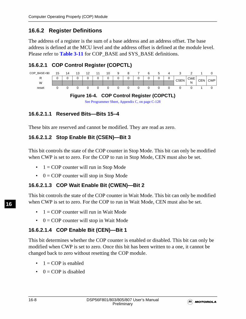
16-8 DSP56F801/803/805/807 User’s Manual�Preliminary
Computer Operating Properly (COP) Module
16
16.6.2 Register Definitions
The address of a register is the sum of a base address and an address offset. The base address is defined at the MCU level and the address offset is defined at the module level. Please refer to Table 3-11 for COP_BASE and SYS_BASE definitions.
16.6.2.1 COP Control Register (COPCTL)
Figure 16-4. COP Control Register (COPCTL)See Programmer Sheet, Appendix C, on page C-128
16.6.2.1.1 Reserved Bits—Bits 15–4
These bits are reserved and cannot be modified. They are read as zero.
16.6.2.1.2 Stop Enable Bit (CSEN)—Bit 3
This bit controls the state of the COP counter in Stop Mode. This bit can only be modified when CWP is set to zero. For the COP to run in Stop Mode, CEN must also be set.
• 1 = COP counter will run in Stop Mode
• 0 = COP counter will stop in Stop Mode
16.6.2.1.3 COP Wait Enable Bit (CWEN)—Bit 2
This bit controls the state of the COP counter in Wait Mode. This bit can only be modified when CWP is set to zero. For the COP to run in Wait Mode, CEN must also be set.
• 1 = COP counter will run in Wait Mode
• 0 = COP counter will stop in Wait Mode
16.6.2.1.4 COP Enable Bit (CEN)—Bit 1
This bit determines whether the COP counter is enabled or disabled. This bit can only be modified when CWP is set to zero. Once this bit has been written to a one, it cannot be changed back to zero without resetting the COP module.
• 1 = COP is enabled
• 0 = COP is disabled
COP_BASE+$0 15 14 13 12 11 10 9 8 7 6 5 4 3 2 1 0
R 0 0 0 0 0 0 0 0 0 0 0 0CSEN
CWEN
CEN CWPW
reset 0 0 0 0 0 0 0 0 0 0 0 0 0 0 1 0
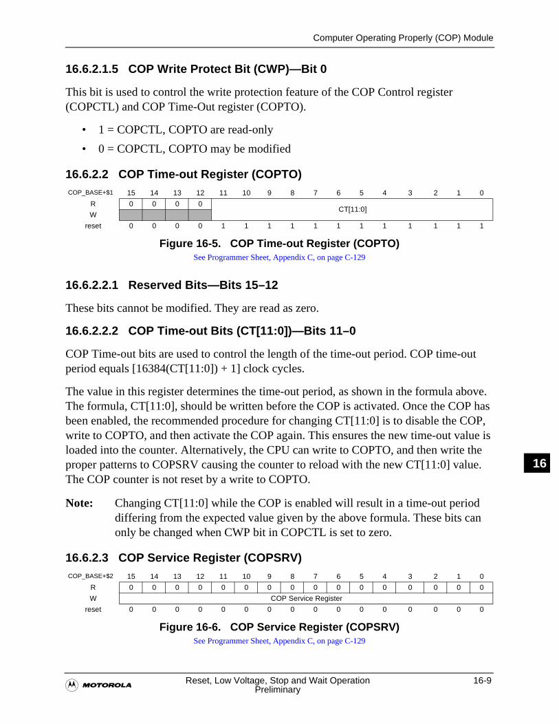
Computer Operating Properly (COP) Module
�Reset, Low Voltage, Stop and Wait Operation 16-9
Preliminary
IN16
16.6.2.1.5 COP Write Protect Bit (CWP)—Bit 0
This bit is used to control the write protection feature of the COP Control register (COPCTL) and COP Time-Out register (COPTO).
• 1 = COPCTL, COPTO are read-only
• 0 = COPCTL, COPTO may be modified
16.6.2.2 COP Time-out Register (COPTO)
Figure 16-5. COP Time-out Register (COPTO)See Programmer Sheet, Appendix C, on page C-129
16.6.2.2.1 Reserved Bits—Bits 15–12
These bits cannot be modified. They are read as zero.
16.6.2.2.2 COP Time-out Bits (CT[11:0])—Bits 11–0
COP Time-out bits are used to control the length of the time-out period. COP time-out period equals [16384(CT[11:0]) + 1] clock cycles.
The value in this register determines the time-out period, as shown in the formula above. The formula, CT[11:0], should be written before the COP is activated. Once the COP has been enabled, the recommended procedure for changing CT[11:0] is to disable the COP, write to COPTO, and then activate the COP again. This ensures the new time-out value is loaded into the counter. Alternatively, the CPU can write to COPTO, and then write the proper patterns to COPSRV causing the counter to reload with the new CT[11:0] value. The COP counter is not reset by a write to COPTO.
Note: Changing CT[11:0] while the COP is enabled will result in a time-out period differing from the expected value given by the above formula. These bits can only be changed when CWP bit in COPCTL is set to zero.
16.6.2.3 COP Service Register (COPSRV)
Figure 16-6. COP Service Register (COPSRV)See Programmer Sheet, Appendix C, on page C-129
COP_BASE+$1 15 14 13 12 11 10 9 8 7 6 5 4 3 2 1 0
R 0 0 0 0CT[11:0]
W
reset 0 0 0 0 1 1 1 1 1 1 1 1 1 1 1 1
COP_BASE+$2 15 14 13 12 11 10 9 8 7 6 5 4 3 2 1 0
R 0 0 0 0 0 0 0 0 0 0 0 0 0 0 0 0
W COP Service Register
reset 0 0 0 0 0 0 0 0 0 0 0 0 0 0 0 0
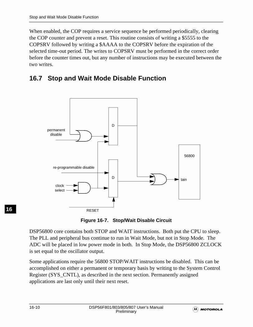
16-10 DSP56F801/803/805/807 User’s Manual�Preliminary
Stop and Wait Mode Disable Function
16
When enabled, the COP requires a service sequence be performed periodically, clearing the COP counter and prevent a reset. This routine consists of writing a $5555 to the COPSRV followed by writing a $AAAA to the COPSRV before the expiration of the selected time-out period. The writes to COPSRV must be performed in the correct order before the counter times out, but any number of instructions may be executed between the two writes.
16.7 Stop and Wait Mode Disable Function
Figure 16-7. Stop/Wait Disable Circuit
DSP56800 core contains both STOP and WAIT instructions. Both put the CPU to sleep. The PLL and peripheral bus continue to run in Wait Mode, but not in Stop Mode. The ADC will be placed in low power mode in both. In Stop Mode, the DSP56800 ZCLOCK is set equal to the oscillator output.
Some applications require the 56800 STOP/WAIT instructions be disabled. This can be accomplished on either a permanent or temporary basis by writing to the System Control Register (SYS_CNTL), as described in the next section. Permanently assigned applications are last only until their next reset.
D
D
56800
tain
clockselect
re-programmable disable
permanent disable
RESET
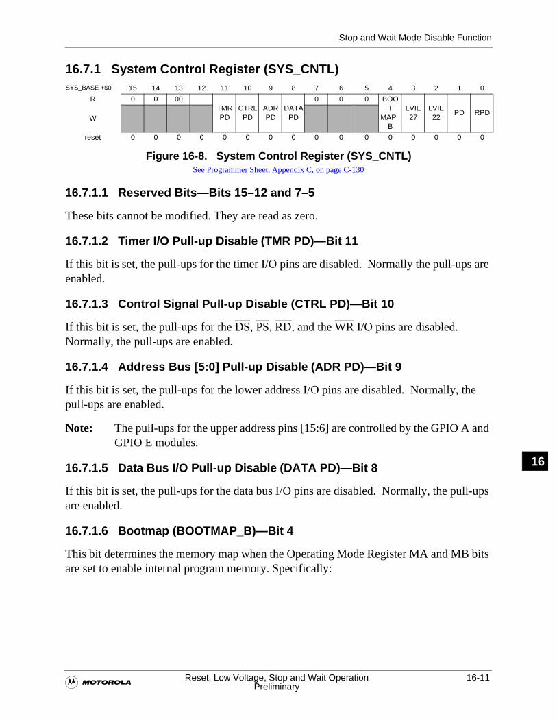
Stop and Wait Mode Disable Function
�Reset, Low Voltage, Stop and Wait Operation 16-11
Preliminary
IN16
16.7.1 System Control Register (SYS_CNTL)
16.7.1.1 Reserved Bits—Bits 15–12 and 7–5
These bits cannot be modified. They are read as zero.
16.7.1.2 Timer I/O Pull-up Disable (TMR PD)—Bit 11
If this bit is set, the pull-ups for the timer I/O pins are disabled. Normally the pull-ups are enabled.
16.7.1.3 Control Signal Pull-up Disable (CTRL PD)—Bit 10
If this bit is set, the pull-ups for the DS, PS, RD, and the WR I/O pins are disabled. Normally, the pull-ups are enabled.
16.7.1.4 Address Bus [5:0] Pull-up Disable (ADR PD)—Bit 9
If this bit is set, the pull-ups for the lower address I/O pins are disabled. Normally, the pull-ups are enabled.
Note: The pull-ups for the upper address pins [15:6] are controlled by the GPIO A and GPIO E modules.
16.7.1.5 Data Bus I/O Pull-up Disable (DATA PD)—Bit 8
If this bit is set, the pull-ups for the data bus I/O pins are disabled. Normally, the pull-ups are enabled.
16.7.1.6 Bootmap (BOOTMAP_B)—Bit 4
This bit determines the memory map when the Operating Mode Register MA and MB bits are set to enable internal program memory. Specifically:
SYS_BASE +$0 15 14 13 12 11 10 9 8 7 6 5 4 3 2 1 0
R 0 0 00TMR PD
CTRL PD
ADR PD
DATA PD
0 0 0 BOOT
MAP_B
LVIE 27
LVIE 22
PD RPDW
reset 0 0 0 0 0 0 0 0 0 0 0 0 0 0 0 0
Figure 16-8. System Control Register (SYS_CNTL)See Programmer Sheet, Appendix C, on page C-130
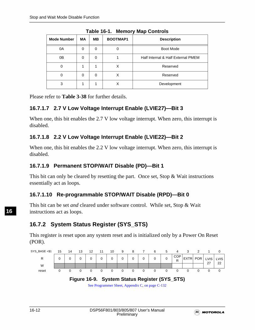
16-12 DSP56F801/803/805/807 User’s Manual�Preliminary
Stop and Wait Mode Disable Function
16
Table 16-1. Memory Map Controls
Please refer to Table 3-38 for further details.
16.7.1.7 2.7 V Low Voltage Interrupt Enable (LVIE27)—Bit 3
When one, this bit enables the 2.7 V low voltage interrupt. When zero, this interrupt is disabled.
16.7.1.8 2.2 V Low Voltage Interrupt Enable (LVIE22)—Bit 2
When one, this bit enables the 2.2 V low voltage interrupt. When zero, this interrupt is disabled.
16.7.1.9 Permanent STOP/WAIT Disable (PD)—Bit 1
This bit can only be cleared by resetting the part. Once set, Stop & Wait instructions essentially act as loops.
16.7.1.10 Re-programmable STOP/WAIT Disable (RPD)—Bit 0
This bit can be set and cleared under software control. While set, Stop & Wait instructions act as loops.
16.7.2 System Status Register (SYS_STS)
This register is reset upon any system reset and is initialized only by a Power On Reset (POR).
Mode Number MA MB BOOTMAP1 Description
0A 0 0 0 Boot Mode
0B 0 0 1 Half Internal & Half External PMEM
0 1 1 X Reserved
0 0 0 X Reserved
3 1 1 X Development
SYS_BASE +$1 15 14 13 12 11 10 9 8 7 6 5 4 3 2 1 0
R 0 0 0 0 0 0 0 0 0 0 0COP
REXTR POR LVIS
27LVIS 22
W
reset 0 0 0 0 0 0 0 0 0 0 0 0 0 0 0 0
Figure 16-9. System Status Register (SYS_STS)See Programmer Sheet, Appendix C, on page C-132
Stop and Wait Mode Disable Function
�Reset, Low Voltage, Stop and Wait Operation 16-13
Preliminary
IN16
16.7.2.1 Reserved Bits—Bits 15–5
These bits cannot be modified. They are read as zero.
16.7.2.2 COP Reset (COPR)—Bit 4
When one, the COPR bit, indicates the Computer Operating Properly (COP) timer generated reset has occurred, this bit will be cleared by a Power on Reset or by software. Writing a zero to this bit position will set the bit, while writing a one to the bit will clear it. Setting this bit will not reset it. In summary, when the COPR bit is one, the previous system reset was caused by the Computer Operating Properly (COP) timer.
16.7.2.3 External Reset (EXTR)—Bit 3
If one, the EXTR bit indicates an external system reset has occurred. This bit will be cleared by a Power On Reset or by software. Writing a zero to this bit position will set the bit while writing a one to the bit position will clear it. Setting this bit will not reset it. Basically, when the EXTR bit is one, the previous system reset was caused by the external RESET pin being asserted low.
16.7.2.4 Power on Reset (POR)—Bit 2
When one, the POR bit indicates a Power On Reset occurred some time in the past. This bit can only be cleared by software. Writing a zero to this bit will set the bit while writing a one to the bit position will clear the bit. Setting this bit will not reset it. In summary, if the bit is one, the previous system reset was due to a power on reset.
16.7.3 2.7 V Low Voltage Interrupt Source (LVIS27)—Bit 1
If one, the LVIS27 bit indicates that a 2.7 V Low Voltage Interrupt is active. Writing a zero to this bit position will set this bit. Writing a one to this bit position will clear this bit. Setting this bit will cause an interrupt if the corresponding interrupt enable bit is set. When one, this bit indicates that the chip voltage has dropped below 2.7 V.
16.7.4 2.2 Low Voltage Interrupt Source (LVIS 22)—Bit 0
If one, the LVIS22 bit indicates that a 2.2 V Low Voltage Interrupt is active. Writing a zero to this bit position will set this bit. Writing a one to this bit position will clear this bit. Setting this bit will cause an interrupt if the corresponding interrupt enable bit is set. When one, this bit indicates that the chip voltage has dropped below 2.2 V.
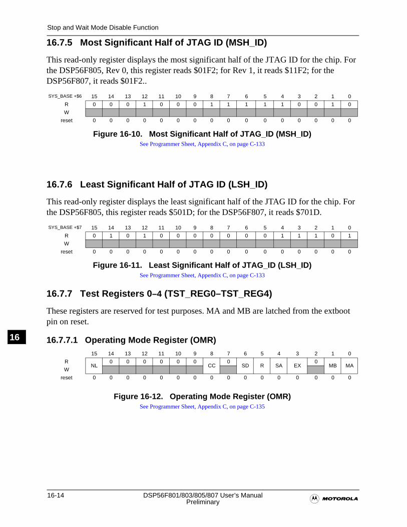
16-14 DSP56F801/803/805/807 User’s Manual�Preliminary
Stop and Wait Mode Disable Function
16
16.7.5 Most Significant Half of JTAG ID (MSH_ID)
This read-only register displays the most significant half of the JTAG ID for the chip. For the DSP56F805, Rev 0, this register reads $01F2; for Rev 1, it reads $11F2; for the DSP56F807, it reads $01F2..
16.7.6 Least Significant Half of JTAG ID (LSH_ID)
This read-only register displays the least significant half of the JTAG ID for the chip. For the DSP56F805, this register reads $501D; for the DSP56F807, it reads $701D.
16.7.7 Test Registers 0–4 (TST_REG0–TST_REG4)
These registers are reserved for test purposes. MA and MB are latched from the extboot pin on reset.
16.7.7.1 Operating Mode Register (OMR)
Figure 16-12. Operating Mode Register (OMR)See Programmer Sheet, Appendix C, on page C-135
SYS_BASE +$6 15 14 13 12 11 10 9 8 7 6 5 4 3 2 1 0
R 0 0 0 1 0 0 0 1 1 1 1 1 0 0 1 0
W
reset 0 0 0 0 0 0 0 0 0 0 0 0 0 0 0 0
Figure 16-10. Most Significant Half of JTAG_ID (MSH_ID)See Programmer Sheet, Appendix C, on page C-133
SYS_BASE +$7 15 14 13 12 11 10 9 8 7 6 5 4 3 2 1 0
R 0 1 0 1 0 0 0 0 0 0 0 1 1 1 0 1
W
reset 0 0 0 0 0 0 0 0 0 0 0 0 0 0 0 0
Figure 16-11. Least Significant Half of JTAG_ID (LSH_ID)See Programmer Sheet, Appendix C, on page C-133
15 14 13 12 11 10 9 8 7 6 5 4 3 2 1 0
RNL
0 0 0 0 0 0CC
0SD R SA EX
0MB MA
W
reset 0 0 0 0 0 0 0 0 0 0 0 0 0 0 0 0
Stop and Wait Mode Disable Function
�Reset, Low Voltage, Stop and Wait Operation 16-15
Preliminary
IN16
16.7.7.2 Nested Looping (NL) Bit–15
The Nested Looping (NL) bit displays the status of program DO looping and the hardware stack. When the NL bit is set, it indicates the program is currently in a nested DO loop. For example, two DO loops are active. When this bit is cleared, it indicates the program is currently not in a nested DO loop and there may be a single active DO loop or no active DO loop. This bit is necessary for saving and restoring the contents of the hardware stack. REP looping does not affect this bit.
It is important to never put the processor in the reserved combination specified in Table 3-8. This combination can be avoided by ensuring the LF bit is never cleared when the NL bit is set. The NL bit is cleared on processor reset.
If both the NL and LF bits are set, two DO loops are active, and a DO instruction is executed, a hardware stack overflow interrupt occurs because there is no more space in the HWS to support a third DO loop.
The NL bit is also affected by any accesses to the HWS. Any MOVE instruction written to this register copies the old contents of the LF bit into the NL bit, then sets the NL bit into the LF bit, sequentially clearing the NL bit.
16.7.7.3 Reserved Bits—Bits 14–9, 7 and 2
These bits may be modified. They read as zero. The bits should be written as zero for future compatibility.
16.7.7.4 Condition Codes (CC)—Bit 8
The Condition Code (CC) bit selects whether condition codes are generated using a 36-bit result from the Multiplier/Accumulator (MAC) array or a 32-bit result. When the CC bit is set, the C, N, V, and Z condition codes are generated based on Bit 31 of the Data Arithmetic Logic Unit (Data ALU) result. When cleared, the C, N, V, and Z condition codes are generated based on Bit 35 of the Data ALU result. The generation of the L, E, and U condition codes is not affected by the CC bit. The CC bit is cleared by processor reset.
Note: The unsigned condition tests used when branching or jumping (HI, HS, LO, or LS) can be used only when the condition codes are generated with the CC bit set. Otherwise, the chip does not generate the unsigned conditions correctly.
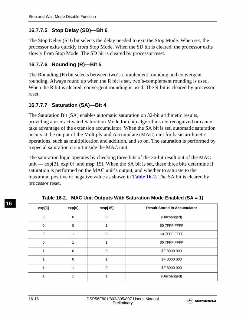
16-16 DSP56F801/803/805/807 User’s Manual�Preliminary
Stop and Wait Mode Disable Function
16
16.7.7.5 Stop Delay (SD)—Bit 6
The Stop Delay (SD) bit selects the delay needed to exit the Stop Mode. When set, the processor exits quickly from Stop Mode. When the SD bit is cleared, the processor exits slowly from Stop Mode. The SD bit is cleared by processor reset.
16.7.7.6 Rounding (R)—Bit 5
The Rounding (R) bit selects between two’s-complement rounding and convergent rounding. Always round up when the R bit is set, two’s-complement rounding is used. When the R bit is cleared, convergent rounding is used. The R bit is cleared by processor reset.
16.7.7.7 Saturation (SA)—Bit 4
The Saturation Bit (SA) enables automatic saturation on 32-bit arithmetic results, providing a user-activated Saturation Mode for chip algorithms not recognized or cannot take advantage of the extension accumulator. When the SA bit is set, automatic saturation occurs at the output of the Multiply and Accumulate (MAC) unit for basic arithmetic operations, such as multiplication and addition, and so on. The saturation is performed by a special saturation circuit inside the MAC unit.
The saturation logic operates by checking three bits of the 36-bit result out of the MAC unit — exp[3], exp[0], and msp[15]. When the SA bit is set, these three bits determine if saturation is performed on the MAC unit’s output, and whether to saturate to the maximum positive or negative value as shown in Table 16-2. The SA bit is cleared by processor reset.
Table 16-2. MAC Unit Outputs With Saturation Mode Enabled (SA = 1)
exp[3] exp[0] msp[15] Result Stored in Accumulator
0 0 0 (Unchanged)
0 0 1 $0 7FFF FFFF
0 1 0 $0 7FFF FFFF
0 1 1 $0 7FFF FFFF
1 0 0 $F 8000 000
1 0 1 $F 8000 000
1 1 0 $F 8000 000
1 1 1 (Unchanged)
Stop and Wait Mode Disable Function
�Reset, Low Voltage, Stop and Wait Operation 16-17
Preliminary
IN16
Note: Saturation Mode is always disabled during the execution of the following instructions: ASLL, ASRR, LSLL, LSRR, ASRAC, LSRAC, IMPY16, MPYSU, MACSU, AND, OR, EOR, NOT, LSL, LSR, ROL, and ROR. For these instructions, no saturation is performed at the output of the MAC unit.
16.7.7.8 External X Memory (EX)—Bit 3
The External X Memory (EX) bit is necessary for providing a continuous memory map when using more than 64K of external data memory. When the EX bit is set, all accesses to X memory on the X Address Bus 1 (XAB1) and Core Global Data Bus (CGDB) or Peripheral Global Data Bus (PGDB) are forced to be external, except when a MOVE or bit-field instruction is executed using the I/O Short Addressing Mode. In this case, the EX bit is ignored, and the access is performed to the on-chip location. When the EX bit is cleared, internal X memory can be accessed with all addressing modes.
The EX bit is ignored by the second read of a dual-read instruction, using the X address Bus two (XAB2) and X Data Bus two (XDB2) and always accesses on-chip X data memory. For instructions with two parallel reads, the second read is always performed to internal on-chip memory.
Note: When the EX bit is set, only the upper sixty four peripheral memory-mapped location are accessible (X:$FF–0$FFFF) with the I/O Short Addressing Mode. The lower sixty-four memory-mapped locations (X:$FF80–$FFBF) are not accessible when the EX bit is set. An access to these addresses results in an access to external memory.
The EX bit is cleared by processor reset.
16.7.7.9 Operating Mode B (MB)—Bit 1
This bit is latched from the MODEB pin on reset.
16.7.7.10 Operating Mode A (MA)—Bit 0
This bit is latched from the MODEA pin on reset.
16-18 DSP56F801/803/805/807 User’s Manual�Preliminary
Stop and Wait Mode Disable Function
16

�OnCE Module 17-1
Preliminary
N17
Chapter 17OnCE Module

17-2 DSP56F801/803/805/807 User’s Manual�Preliminary
N17
Features
�OnCE Module 17-3
Preliminary
N17
17.1 Introduction
Chapter 17 describes the DSP56F800 core-based family chips providing board and chip-level testing capability through two on-chip modules. Both modules are accessed through the JTAG/OnCETM port. The modules are:
• On-Chip Emulation (OnCE) module
• Test Access Port (TAP) and 16-state controller, known also as the Joint Test Action Group (JTAG) port
The presence of the JTAG/OnCE port permits users to insert the Digital Signal Processor (DSP) chip into a target system while retaining Debug control. This capability is especially important for devices without an external bus, thereby eliminating the need for an expensive cable bringing out the chip footprint required by a traditional emulator system. Additionally, on DSP56F 801 through 807, the JTAG/OnCE port can be used to program the internal Flash memory On-Chip Emulation (OnCE) module.
17.2 Features
The On-Chip Emulation (OnCE) module is a Motorola-designed module used in DSP chips to Debug application software used with the chip. The module is a separate on-chip block allowing non-intrusive interaction with the DSP, with the accessibility through the pins of the JTAG interface. The OnCE module makes it possible to examine registers, memory, or on-chip peripherals’ contents in a special Debug environment. This avoids sacrificing any user-accessible on-chip resources to perform debugging.
The capabilities of the OnCE module include the ability to:
• Interrupt or break into Debug Mode on a program memory address: fetch, read, write, or access
• Interrupt or break into Debug ModeMode on a data memory address: read, write, or access
• Interrupt or break into Debug Mode on an on-chip peripheral register access: read, write, or access
• Enter Debug Mode using a DSP microprocessor instruction
• Display or modify the contents of any DSP core register
• Display or modify the contents of peripheral memory-mapped registers
• Display or modify any desired sections of program or data memory
• Trace one, single stepping, or as many as 256 instructions
• Save or restore the current state of the DSP chip’s pipeline
17-4 DSP56F801/803/805/807 User’s Manual�Preliminary
Features
N17
• Display the contents of the real-time instruction trace buffer, whether in Debug Mode or not
• Return to User Mode from Debug Mode
• Set up breakpoints without being in Debug Mode
• Set hardware breakpoints, software breakpoints, and trace occurrences (OnCE events) possibly forcing the chip into Debug Mode, force a vectored interrupt, force the real-time instruction buffer to halt, or toggle a pin, based on the user’s needs
Please refer to Section 17.6 for a detailed description of this port.
Joint Test Action Group (JTAG) Port
The Joint Test Action Group (JTAG) port is a dedicated user-accessible Test Access Port (TAP) compatible with the IEEE 1149.1a-1993 Standard Test Access Port and Boundary Scan Architecture. Problems associated with testing high-density circuit boards have led to the development of this proposed standard under the sponsorship of the Test Technology Committee of IEEE and the JTAG. The DSP56F801/803/805/807 supports circuit board test strategies based on this standard.
Five dedicated pins interface to a Test Access Port (TAP) containing a 16-state controller. The TAP uses a boundary scan technique to test the interconnections between integrated circuits after they are assembled onto a Printed Circuit Board. Boundary scan allows a tester to observe and control signal levels at each component pin through a shift register placed next to each pin. This is important for testing continuity and determining if pins are stuck at a one or zero level.
The TAP port has the following capabilities:
• Perform boundary scan operations to test circuit board electrical continuity
• Bypass the DSP for a given circuit board test by replacing the Boundary Scan Register (BSR) with a single-bit register
• Provide a means of accessing the OnCE module controller and circuits to control a target system
• Disable the output drive to pins during circuit board testing
• Sample the DSP system pins during operation, and shift out the result in the BSR; preload values outputing pins prior to invoking the EXTEST instruction
• Query identification information, manufacturer, part number, and version from a DSP chip
• Force test data onto the outputs of a DSP IC, while replacing its BSR in the serial data path with a single-bit register
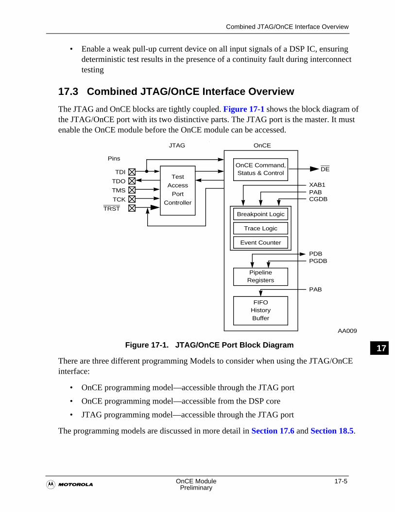
Combined JTAG/OnCE Interface Overview
�OnCE Module 17-5
Preliminary
N17
• Enable a weak pull-up current device on all input signals of a DSP IC, ensuring deterministic test results in the presence of a continuity fault during interconnect testing
17.3 Combined JTAG/OnCE Interface Overview
The JTAG and OnCE blocks are tightly coupled. Figure 17-1 shows the block diagram of the JTAG/OnCE port with its two distinctive parts. The JTAG port is the master. It must enable the OnCE module before the OnCE module can be accessed.
There are three different programming Models to consider when using the JTAG/OnCE interface:
• OnCE programming model—accessible through the JTAG port
• OnCE programming model—accessible from the DSP core
• JTAG programming model—accessible through the JTAG port
The programming models are discussed in more detail in Section 17.6 and Section 18.5.
\
Figure 17-1. JTAG/OnCE Port Block Diagram
JTAG
PipelineRegisters
PAB
FIFOHistoryBuffer
OnCE Command,Status & Control
CGDB
PAB
PDBPGDB
Breakpoint Logic
Trace Logic
Event Counter
OnCE
TDO
TMS
TCK
TRST
TDI
Pins
Test
Access
Port
Controller
XAB1
AA009
DE
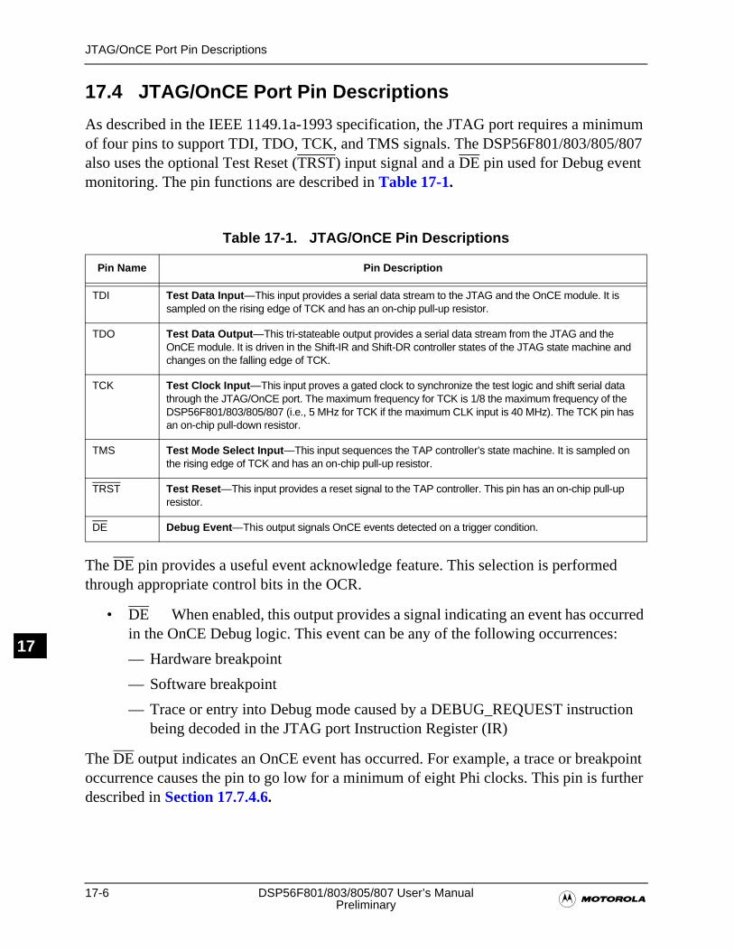
17-6 DSP56F801/803/805/807 User’s Manual�Preliminary
JTAG/OnCE Port Pin Descriptions
N17
17.4 JTAG/OnCE Port Pin Descriptions
As described in the IEEE 1149.1a-1993 specification, the JTAG port requires a minimum of four pins to support TDI, TDO, TCK, and TMS signals. The DSP56F801/803/805/807 also uses the optional Test Reset (TRST) input signal and a DE pin used for Debug event monitoring. The pin functions are described in Table 17-1.
The DE pin provides a useful event acknowledge feature. This selection is performed through appropriate control bits in the OCR.
• DE When enabled, this output provides a signal indicating an event has occurred in the OnCE Debug logic. This event can be any of the following occurrences:
— Hardware breakpoint
— Software breakpoint
— Trace or entry into Debug mode caused by a DEBUG_REQUEST instruction being decoded in the JTAG port Instruction Register (IR)
The DE output indicates an OnCE event has occurred. For example, a trace or breakpoint occurrence causes the pin to go low for a minimum of eight Phi clocks. This pin is further described in Section 17.7.4.6.
Table 17-1. JTAG/OnCE Pin Descriptions
Pin Name Pin Description
TDI Test Data Input—This input provides a serial data stream to the JTAG and the OnCE module. It is sampled on the rising edge of TCK and has an on-chip pull-up resistor.
TDO Test Data Output—This tri-stateable output provides a serial data stream from the JTAG and the OnCE module. It is driven in the Shift-IR and Shift-DR controller states of the JTAG state machine and changes on the falling edge of TCK.
TCK Test Clock Input—This input proves a gated clock to synchronize the test logic and shift serial data through the JTAG/OnCE port. The maximum frequency for TCK is 1/8 the maximum frequency of the DSP56F801/803/805/807 (i.e., 5 MHz for TCK if the maximum CLK input is 40 MHz). The TCK pin has an on-chip pull-down resistor.
TMS Test Mode Select Input—This input sequences the TAP controller’s state machine. It is sampled on the rising edge of TCK and has an on-chip pull-up resistor.
TRST Test Reset—This input provides a reset signal to the TAP controller. This pin has an on-chip pull-up resistor.
DE Debug Event—This output signals OnCE events detected on a trigger condition.
OnCE Module Architecture
�OnCE Module 17-7
Preliminary
N17
When the JTAGIR does not contain an ENABLE_ONCE instruction, the OCR control bits are reset only by assertion of RESET or COP timer reset. When the ENABLE_ONCE instruction is in the JTAGIR at the time of reset, the OCR bits are not modified.
17.5 Register Summary
The OnCE module of the DSP56F801/803/805/807 have the following registers:
• OnCE Breakpoint Address Register (OBAR)
• OnCE Breakpoint Address Register 2 (OBAR2)
• OnCE Breakpoint Control Register 2 (OBCTL2)
• OnCE Command Register (OCMDR)
• OnCE Breakpoint Mask Register 2 (OBMSK2)
• OnCE Count Register (OCNTR)
• OnCE Control Register (OCR)
• OnCE Decoder (ODEC) (not memory mapped)
• OnCE Memory Address Comparator (OMAC) (not memory mapped)
• OnCE Memory Address Comparator 2 (OMAC2) (not memory mapped)
• OnCE Memory Address Latch (OMAL) (not memory mapped)
• OnCE Memory Address Latch 2 (OMAL2) (not memory mapped)
• OnCE PAB (Program Address Bus) Decode Register (OPABDR)
• OnCE PAB (Program Address Bus) Execute Register (OPABER)
• OnCE PAB (Program Address Bus) Fetch Register (OPABFR)
• OnCE PDB (Program Data Bus) Register (OPDBR)
• OnCE PAB Change of Flow (OPFIFO) (not memory mapped)
• OnCE PDGB (Program Global Data Bus) Register (OPGDBR)
• OnCE Shift Register (OSHR) (not memory mapped)
• OnCE Status Register (OSR)
17.6 OnCE Module Architecture
While the JTAG port described in Section 18.5 provides board test capability, the OnCE module provides emulation and Debug capability to the user. The OnCE module permits full-speed, non-intrusive emulation on a user’s target system or on a Motorola Evaluation Module (EVM) board.
17-8 DSP56F801/803/805/807 User’s Manual�Preliminary
OnCE Module Architecture
N17
A typical Debug environment consists of a target system where the DSP resides in the user-defined hardware. The DSP’s JTAG port interfaces to a Command Converter board over a seven-wire link, consisting of the five JTAG serial lines, a ground, and reset wire. The reset wire is optional and is only used to reset the DSP and its associated circuitry.
The OnCE module is composed of four different sub-blocks, each performing a different task:
• Command, status, and control
• Breakpoint and trace
• Pipeline registers
• FIFO history buffer
A block diagram of the OnCE module is shown in Figure 17-2. The registers serially shift information from TDI to TDO through the OnCE Shift Register (OSHR). Figure 17-3 displays the OnCE module registers accessible through the JTAG port. Figure 17-4 exhibits the OnCE module registers accessible through the DSP core and its corresponding OnCE interrupt vector.
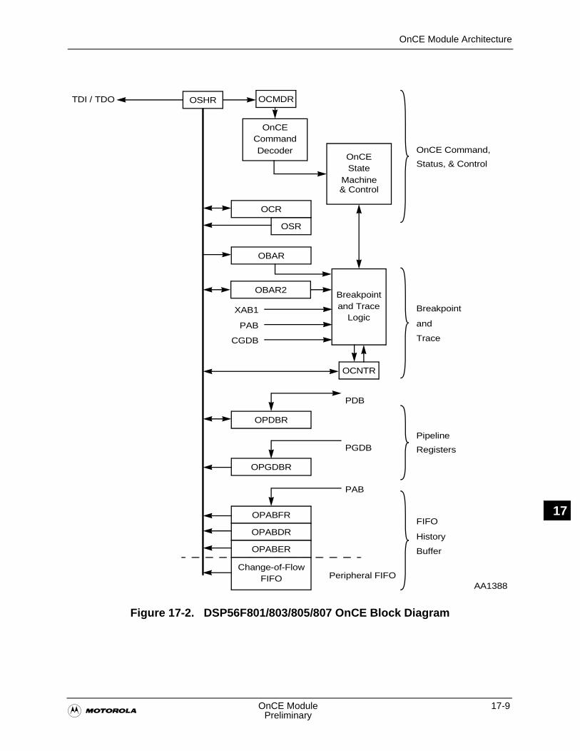
OnCE Module Architecture
�OnCE Module 17-9
Preliminary
N17
Figure 17-2. DSP56F801/803/805/807 OnCE Block Diagram
TDI / TDO
OPABFR
OPABDR
OPDBR
OBAR
OCNTR
OSR
OCMDR
OCR
PAB
XAB1
OPGDBR
PDB
PGDB
PAB
OnCE Command,
Status, & Control
Breakpoint
and
Trace
Pipeline
Registers
FIFO
History
BufferOPABER
Change-of-FlowFIFO
Breakpointand Trace
OnCEState
Machine
OnCECommandDecoder
& Control
Logic
Peripheral FIFO
CGDB
OBAR2
OSHR
AA1388
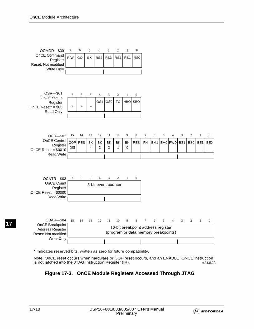
17-10 DSP56F801/803/805/807 User’s Manual�Preliminary
OnCE Module Architecture
N17
Figure 17-3. OnCE Module Registers Accessed Through JTAG
OSR—$01OnCE Status
RegisterOnCE Reset* = $00
Read Only* * *
OS1 OS0 TO HBO SBO
7 6 5 4 3 2 1 0
OCR—$02OnCE Control
RegisterOnCE Reset = $0010
Read/Write
BK
2
BK
1
BK
0
RES FH EM1 EM0 PWD BS1 BS0 BE1 BE0COP
DIS
RES BK
4
BK
3
11 10 9 8 7 6 5 4 3 2 1 015 14 13 12
OCMDR—$00OnCE Command
RegisterReset: Not modified
Write Only
R/W GO EX RS4 RS3 RS2 RS1 RS0
7 6 5 4 3 2 1 0
OCNTR—$03OnCE Count
RegisterOnCE Reset = $0000
Read/Write
8-bit event counter
7 6 5 4 3 2 1 0
* Indicates reserved bits, written as zero for future compatibility.
OBAR—$04OnCE BreakpointAddress Register
Reset: Not modifiedWrite Only
16-bit breakpoint address register(program or data memory breakpoints)
11 10 9 8 7 6 5 4 3 2 1 015 14 13 12
Note: OnCE reset occurs when hardware or COP reset occurs, and an ENABLE_ONCE instruction is not latched into the JTAG Instruction Register (IR). AA1389A
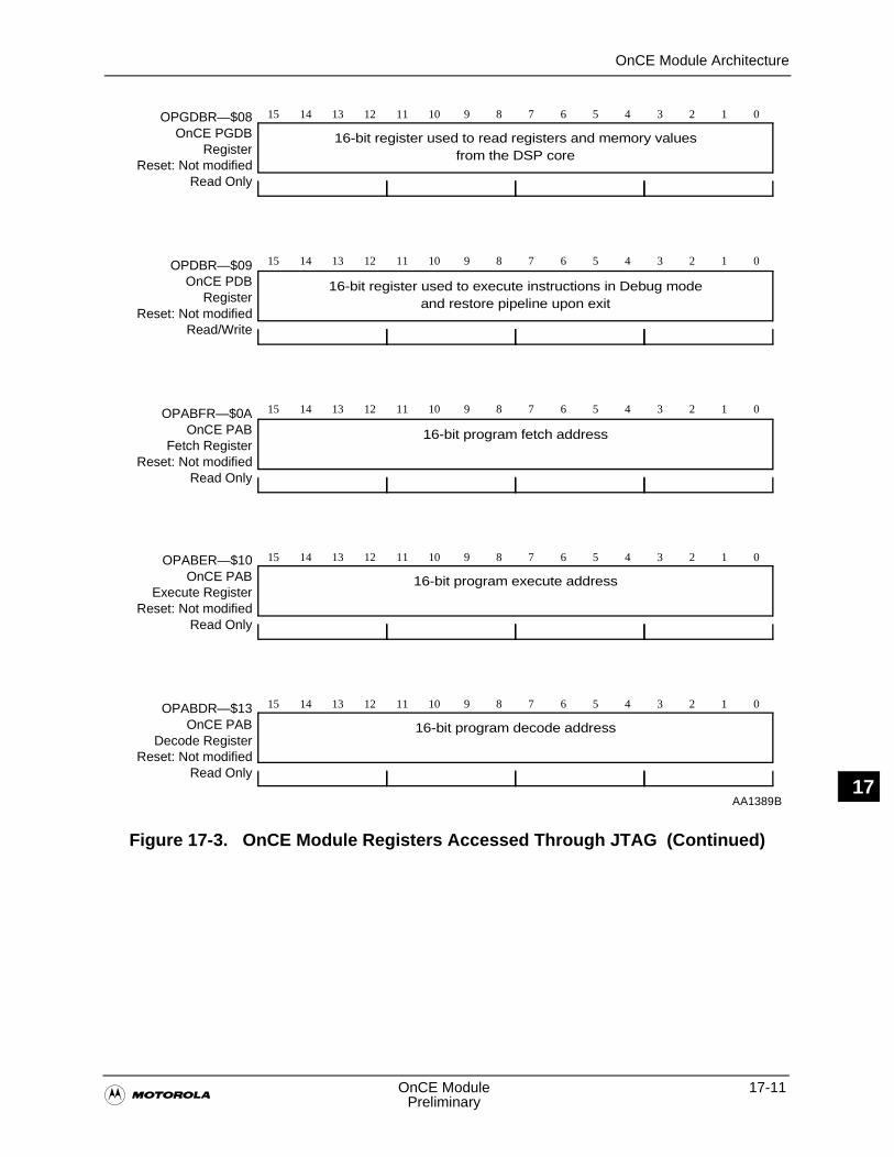
OnCE Module Architecture
�OnCE Module 17-11
Preliminary
N17
Figure 17-3. OnCE Module Registers Accessed Through JTAG (Continued)
OPABDR—$13OnCE PAB
Decode RegisterReset: Not modified
Read Only
16-bit program decode address
11 10 9 8 7 6 5 4 3 2 1 015 14 13 12
OPABFR—$0AOnCE PAB
Fetch RegisterReset: Not modified
Read Only
16-bit program fetch address
11 10 9 8 7 6 5 4 3 2 1 015 14 13 12
OPGDBR—$08OnCE PGDB
RegisterReset: Not modified
Read Only
16-bit register used to read registers and memory valuesfrom the DSP core
11 10 9 8 7 6 5 4 3 2 1 015 14 13 12
OPDBR—$09OnCE PDB
RegisterReset: Not modified
Read/Write
16-bit register used to execute instructions in Debug modeand restore pipeline upon exit
11 10 9 8 7 6 5 4 3 2 1 015 14 13 12
OPABER—$10OnCE PAB
Execute RegisterReset: Not modified
Read Only
16-bit program execute address
11 10 9 8 7 6 5 4 3 2 1 015 14 13 12
AA1389B
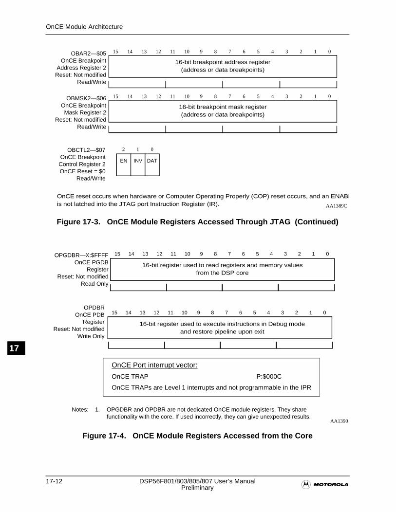
17-12 DSP56F801/803/805/807 User’s Manual�Preliminary
OnCE Module Architecture
N17
Figure 17-4. OnCE Module Registers Accessed from the Core
Figure 17-3. OnCE Module Registers Accessed Through JTAG (Continued)
OBMSK2—$06OnCE BreakpointMask Register 2
Reset: Not modifiedRead/Write
16-bit breakpoint mask register(address or data breakpoints)
11 10 9 8 7 6 5 4 3 2 1 015 14 13 12
OBCTL2—$07OnCE Breakpoint
Control Register 2OnCE Reset = $0
Read/Write
EN INV DAT
2 1 0
OBAR2—$05OnCE Breakpoint
Address Register 2Reset: Not modified
Read/Write
16-bit breakpoint address register(address or data breakpoints)
11 10 9 8 7 6 5 4 3 2 1 015 14 13 12
is not latched into the JTAG port Instruction Register (IR). OnCE reset occurs when hardware or Computer Operating Properly (COP) reset occurs, and an ENABL
AA1389C
OPGDBR—X:$FFFFOnCE PGDB
RegisterReset: Not modified
Read Only
16-bit register used to read registers and memory valuesfrom the DSP core
11 10 9 8 7 6 5 4 3 2 1 015 14 13 12
OPDBROnCE PDB
RegisterReset: Not modified
Write Only
11 10 9 8 7 6 5 4 3 2 1 015 14 13 12
16-bit register used to execute instructions in Debug modeand restore pipeline upon exit
OnCE Port interrupt vector:
OnCE TRAP P:$000C
OnCE TRAPs are Level 1 interrupts and not programmable in the IPR
Notes: 1. OPGDBR and OPDBR are not dedicated OnCE module registers. They share functionality with the core. If used incorrectly, they can give unexpected results.
AA1390
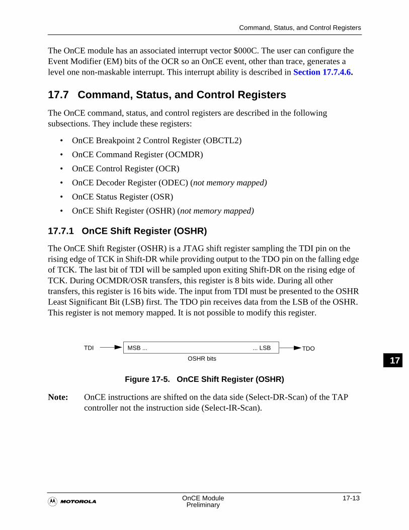
Command, Status, and Control Registers
�OnCE Module 17-13
Preliminary
N17
The OnCE module has an associated interrupt vector $000C. The user can configure the Event Modifier (EM) bits of the OCR so an OnCE event, other than trace, generates a level one non-maskable interrupt. This interrupt ability is described in Section 17.7.4.6.
17.7 Command, Status, and Control Registers
The OnCE command, status, and control registers are described in the following subsections. They include these registers:
• OnCE Breakpoint 2 Control Register (OBCTL2)
• OnCE Command Register (OCMDR)
• OnCE Control Register (OCR)
• OnCE Decoder Register (ODEC) (not memory mapped)
• OnCE Status Register (OSR)
• OnCE Shift Register (OSHR) (not memory mapped)
17.7.1 OnCE Shift Register (OSHR)
The OnCE Shift Register (OSHR) is a JTAG shift register sampling the TDI pin on the rising edge of TCK in Shift-DR while providing output to the TDO pin on the falling edge of TCK. The last bit of TDI will be sampled upon exiting Shift-DR on the rising edge of TCK. During OCMDR/OSR transfers, this register is 8 bits wide. During all other transfers, this register is 16 bits wide. The input from TDI must be presented to the OSHR Least Significant Bit (LSB) first. The TDO pin receives data from the LSB of the OSHR. This register is not memory mapped. It is not possible to modify this register.
Figure 17-5. OnCE Shift Register (OSHR)
Note: OnCE instructions are shifted on the data side (Select-DR-Scan) of the TAP controller not the instruction side (Select-IR-Scan).
TDOTDI
OSHR bits
MSB ... ... LSB
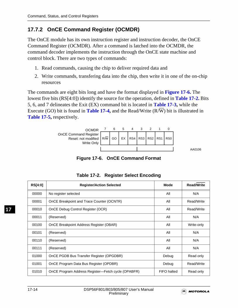
17-14 DSP56F801/803/805/807 User’s Manual�Preliminary
Command, Status, and Control Registers
N17
17.7.2 OnCE Command Register (OCMDR)
The OnCE module has its own instruction register and instruction decoder, the OnCE Command Register (OCMDR). After a command is latched into the OCMDR, the command decoder implements the instruction through the OnCE state machine and control block. There are two types of commands:
1. Read commands, causing the chip to deliver required data and
2. Write commands, transfering data into the chip, then write it in one of the on-chip resources
The commands are eight bits long and have the format displayed in Figure 17-6. The lowest five bits (RS[4:0]) identify the source for the operation, defined in Table 17-2. Bits 5, 6, and 7 delineates the Exit (EX) command bit is located in Table 17-3, while the Execute (GO) bit is found in Table 17-4, and the Read/Write (R/W) bit is illustrated in Table 17-5, respectively.
Figure 17-6. OnCE Command Format
Table 17-2. Register Select Encoding
RS[4:0] Register/Action Selected Mode Read/Write
00000 No register selected All N/A
00001 OnCE Breakpoint and Trace Counter (OCNTR) All Read/Write
00010 OnCE Debug Control Register (OCR) All Read/Write
00011 (Reserved) All N/A
00100 OnCE Breakpoint Address Register (OBAR) All Write-only
00101 (Reserved) All N/A
00110 (Reserved) All N/A
00111 (Reserved) All N/A
01000 OnCE PGDB Bus Transfer Register (OPGDBR) Debug Read only
01001 OnCE Program Data Bus Register (OPDBR) Debug Read/Write
01010 OnCE Program Address Register—Fetch cycle (OPABFR) FIFO halted Read only
OCMDROnCE Command Register
Reset: not modifiedWrite Only
R/W GO EX RS4 RS3 RS2 RS1 RS0
7 6 5 4 3 2 1 0
AA0106
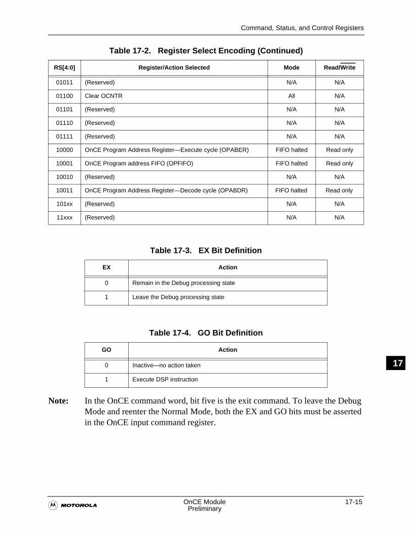
Command, Status, and Control Registers
�OnCE Module 17-15
Preliminary
N17
Note: In the OnCE command word, bit five is the exit command. To leave the Debug Mode and reenter the Normal Mode, both the EX and GO bits must be asserted in the OnCE input command register.
01011 (Reserved) N/A N/A
01100 Clear OCNTR All N/A
01101 (Reserved) N/A N/A
01110 (Reserved) N/A N/A
01111 (Reserved) N/A N/A
10000 OnCE Program Address Register—Execute cycle (OPABER) FIFO halted Read only
10001 OnCE Program address FIFO (OPFIFO) FIFO halted Read only
10010 (Reserved) N/A N/A
10011 OnCE Program Address Register—Decode cycle (OPABDR) FIFO halted Read only
101xx (Reserved) N/A N/A
11xxx (Reserved) N/A N/A
Table 17-3. EX Bit Definition
EX Action
0 Remain in the Debug processing state
1 Leave the Debug processing state
Table 17-4. GO Bit Definition
GO Action
0 Inactive—no action taken
1 Execute DSP instruction
Table 17-2. Register Select Encoding (Continued)
RS[4:0] Register/Action Selected Mode Read/Write
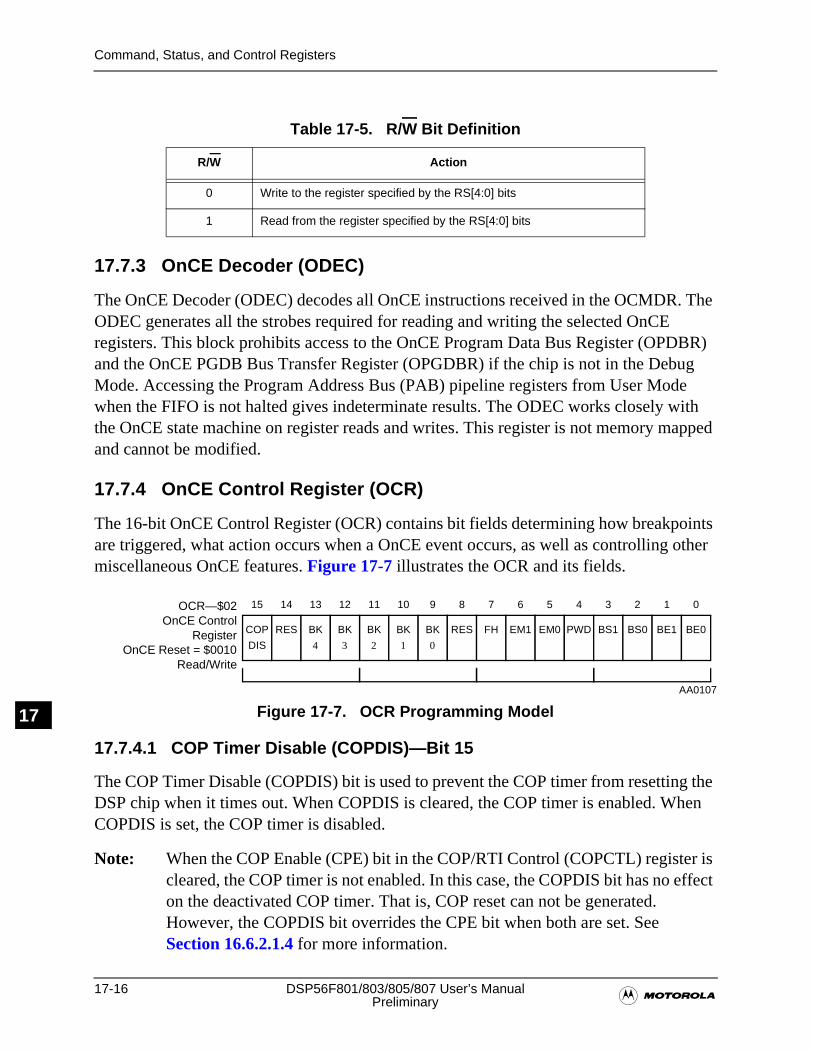
17-16 DSP56F801/803/805/807 User’s Manual�Preliminary
Command, Status, and Control Registers
N17
17.7.3 OnCE Decoder (ODEC)
The OnCE Decoder (ODEC) decodes all OnCE instructions received in the OCMDR. The ODEC generates all the strobes required for reading and writing the selected OnCE registers. This block prohibits access to the OnCE Program Data Bus Register (OPDBR) and the OnCE PGDB Bus Transfer Register (OPGDBR) if the chip is not in the Debug Mode. Accessing the Program Address Bus (PAB) pipeline registers from User Mode when the FIFO is not halted gives indeterminate results. The ODEC works closely with the OnCE state machine on register reads and writes. This register is not memory mapped and cannot be modified.
17.7.4 OnCE Control Register (OCR)
The 16-bit OnCE Control Register (OCR) contains bit fields determining how breakpoints are triggered, what action occurs when a OnCE event occurs, as well as controlling other miscellaneous OnCE features. Figure 17-7 illustrates the OCR and its fields.
17.7.4.1 COP Timer Disable (COPDIS)—Bit 15
The COP Timer Disable (COPDIS) bit is used to prevent the COP timer from resetting the DSP chip when it times out. When COPDIS is cleared, the COP timer is enabled. When COPDIS is set, the COP timer is disabled.
Note: When the COP Enable (CPE) bit in the COP/RTI Control (COPCTL) register is cleared, the COP timer is not enabled. In this case, the COPDIS bit has no effect on the deactivated COP timer. That is, COP reset can not be generated. However, the COPDIS bit overrides the CPE bit when both are set. See Section 16.6.2.1.4 for more information.
Table 17-5. R/W Bit Definition
R/W Action
0 Write to the register specified by the RS[4:0] bits
1 Read from the register specified by the RS[4:0] bits
Figure 17-7. OCR Programming Model
OCR—$02OnCE Control
RegisterOnCE Reset = $0010
Read/Write
BK
2
BK
1
BK
0
RES FH EM1 EM0 PWD BS1 BS0 BE1 BE0COP
DIS
RES BK
4
BK
3
11 10 9 8 7 6 5 4 3 2 1 015 14 13 12
AA0107
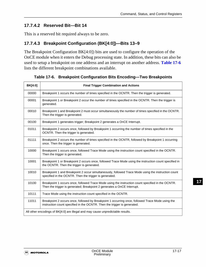
Command, Status, and Control Registers
�OnCE Module 17-17
Preliminary
N17
17.7.4.2 Reserved Bit—Bit 14
This is a reserved bit required always to be zero.
17.7.4.3 Breakpoint Configuration (BK[4:0])—Bits 13–9
The Breakpoint Configuration BK[4:0]) bits are used to configure the operation of the OnCE module when it enters the Debug processing state. In addition, these bits can also be used to setup a breakpoint on one address and an interrupt on another address. Table 17-6 lists the different breakpoint combinations available.
Table 17-6. Breakpoint Configuration Bits Encoding—Two Breakpoints
BK[4:0] Final Trigger Combination and Actions
00000 Breakpoint 1 occurs the number of times specified in the OCNTR. Then the trigger is generated.
00001 Breakpoint 1 or Breakpoint 2 occur the number of times specified in the OCNTR. Then the trigger is generated.
00010 Breakpoint 1 and Breakpoint 2 must occur simultaneously the number of times specified in the OCNTR. Then the trigger is generated.
00100 Breakpoint 1 generates trigger; Breakpoint 2 generates a OnCE Interrupt.
01011 Breakpoint 2 occurs once, followed by Breakpoint 1 occurring the number of times specified in the OCNTR. Then the trigger is generated.
01111 Breakpoint 2 occurs the number of times specified in the OCNTR, followed by Breakpoint 1 occurring once. Then the trigger is generated.
10000 Breakpoint 1 occurs once, followed Trace Mode using the instruction count specified in the OCNTR. Then the trigger is generated.
10001 Breakpoint 1 or Breakpoint 2 occurs once, followed Trace Mode using the instruction count specified in the OCNTR. Then the trigger is generated.
10010 Breakpoint 1 and Breakpoint 2 occur simultaneously, followed Trace Mode using the instruction count specified in the OCNTR. Then the trigger is generated.
10100 Breakpoint 1 occurs once, followed Trace Mode using the instruction count specified in the OCNTR. Then the trigger is generated; Breakpoint 2 generates a OnCE Interrupt.
10111 Trace Mode using the instruction count specified in the OCNTR.
11011 Breakpoint 2 occurs once, followed by Breakpoint 1 occurring once, followed Trace Mode using the instruction count specified in the OCNTR. Then the trigger is generated.
All other encodings of BK[4:0] are illegal and may cause unpredictable results.
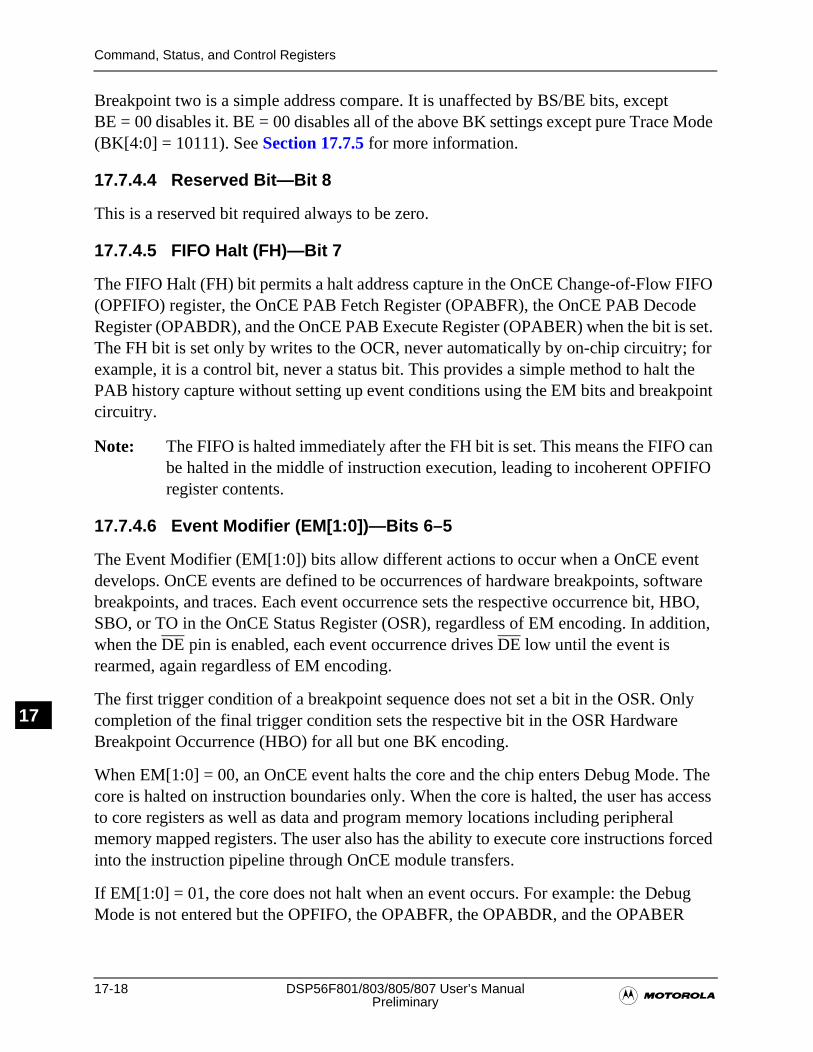
17-18 DSP56F801/803/805/807 User’s Manual�Preliminary
Command, Status, and Control Registers
N17
Breakpoint two is a simple address compare. It is unaffected by BS/BE bits, except BE = 00 disables it. BE = 00 disables all of the above BK settings except pure Trace Mode (BK[4:0] = 10111). See Section 17.7.5 for more information.
17.7.4.4 Reserved Bit—Bit 8
This is a reserved bit required always to be zero.
17.7.4.5 FIFO Halt (FH)—Bit 7
The FIFO Halt (FH) bit permits a halt address capture in the OnCE Change-of-Flow FIFO (OPFIFO) register, the OnCE PAB Fetch Register (OPABFR), the OnCE PAB Decode Register (OPABDR), and the OnCE PAB Execute Register (OPABER) when the bit is set. The FH bit is set only by writes to the OCR, never automatically by on-chip circuitry; for example, it is a control bit, never a status bit. This provides a simple method to halt the PAB history capture without setting up event conditions using the EM bits and breakpoint circuitry.
Note: The FIFO is halted immediately after the FH bit is set. This means the FIFO can be halted in the middle of instruction execution, leading to incoherent OPFIFO register contents.
17.7.4.6 Event Modifier (EM[1:0])—Bits 6–5
The Event Modifier (EM[1:0]) bits allow different actions to occur when a OnCE event develops. OnCE events are defined to be occurrences of hardware breakpoints, software breakpoints, and traces. Each event occurrence sets the respective occurrence bit, HBO, SBO, or TO in the OnCE Status Register (OSR), regardless of EM encoding. In addition, when the DE pin is enabled, each event occurrence drives DE low until the event is rearmed, again regardless of EM encoding.
The first trigger condition of a breakpoint sequence does not set a bit in the OSR. Only completion of the final trigger condition sets the respective bit in the OSR Hardware Breakpoint Occurrence (HBO) for all but one BK encoding.
When EM[1:0] = 00, an OnCE event halts the core and the chip enters Debug Mode. The core is halted on instruction boundaries only. When the core is halted, the user has access to core registers as well as data and program memory locations including peripheral memory mapped registers. The user also has the ability to execute core instructions forced into the instruction pipeline through OnCE module transfers.
If EM[1:0] = 01, the core does not halt when an event occurs. For example: the Debug Mode is not entered but the OPFIFO, the OPABFR, the OPABDR, and the OPABER
Command, Status, and Control Registers
�OnCE Module 17-19
Preliminary
N17
registers stop capturing. This allows access to the PAB history information while the application continues to execute.
If EM[1:0] = 10, the core does not halt when an event occurs, but a level one interrupt occurs with a vector at location P:$000C. This permits diagnostic subroutines execution upon event occurrences, or even to patch program memory by setting a breakpoint at the beginning of the code to be patched.
Note: Trace occurrences do not trigger vectored interrupts. Only hardware and software breakpoints are allowed OnCE events for this EM encoding.
If EM[1:0] = 11, the core does not halt and no other action is taken other than the pulsing low of DE when enabled. This encoding serves to produce an external trigger without changing OnCE module or core operation.
EM encodings 11 and 10 enable automatic event rearming. What this means is: eight Phi clock cycles after the event occurrence flag HBO, TO, or SBO is set, it is reset, thus rearming the event. If DE is enabled, it is asserted, or driven low for eight Phi clock cycles, then released. If another event occurs within those eight Phi clock cycles or immediately after the cycles, the occurrence flag is promptly set and DE remains low.
To rearm an event in EM encoding 00, Debug Mode must be exited, typically by executing a core instruction when setting EX and GO in the OCMDR, thereby clearing the status bits and releasing DE.
To rearm an event in EM encoding 10, the OCR must be written. If the OCR value is to remain constant, writing OCR with its current value successfully rearms the event. When DE is activated and released rearming occurs.
Enabling trace for EM = 11 or EM = 10 is not particularly useful. Since a trace event occurs on every instruction execution once OCNTR reaches 0, the event is continuously set, meaning DE stays low after the first event. For EM = 10, vectoring is disabled on trace occurrences, though DE goes low and stays low after the first trace occurrence. The appropriate event occurrence bit is not reset in this case, tracing and OCNTR = $0000, until Trace Mode is disabled and an event-clearing action takes place, such as exiting Debug Mode or writing the OCR while in User Mode.
Note: Any OCR write in User Mode resets the event flags, while OCR writes in Debug Mode, do not reset the event flags.
Table 17-7 summarizes the different EM encodings.
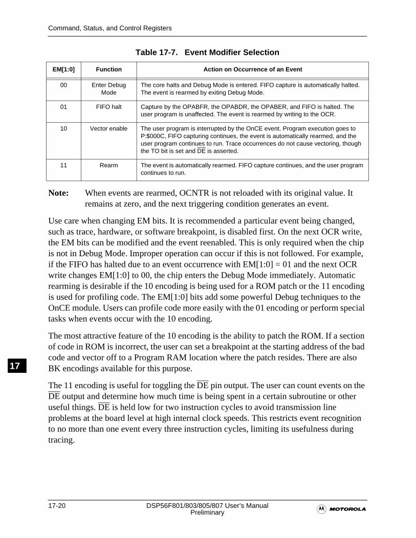
17-20 DSP56F801/803/805/807 User’s Manual�Preliminary
Command, Status, and Control Registers
N17
Note: When events are rearmed, OCNTR is not reloaded with its original value. It remains at zero, and the next triggering condition generates an event.
Use care when changing EM bits. It is recommended a particular event being changed, such as trace, hardware, or software breakpoint, is disabled first. On the next OCR write, the EM bits can be modified and the event reenabled. This is only required when the chip is not in Debug Mode. Improper operation can occur if this is not followed. For example, if the FIFO has halted due to an event occurrence with EM[1:0] = 01 and the next OCR write changes EM[1:0] to 00, the chip enters the Debug Mode immediately. Automatic rearming is desirable if the 10 encoding is being used for a ROM patch or the 11 encoding is used for profiling code. The EM[1:0] bits add some powerful Debug techniques to the OnCE module. Users can profile code more easily with the 01 encoding or perform special tasks when events occur with the 10 encoding.
The most attractive feature of the 10 encoding is the ability to patch the ROM. If a section of code in ROM is incorrect, the user can set a breakpoint at the starting address of the bad code and vector off to a Program RAM location where the patch resides. There are also BK encodings available for this purpose.
The 11 encoding is useful for toggling the DE pin output. The user can count events on the DE output and determine how much time is being spent in a certain subroutine or other useful things. DE is held low for two instruction cycles to avoid transmission line problems at the board level at high internal clock speeds. This restricts event recognition to no more than one event every three instruction cycles, limiting its usefulness during tracing.
Table 17-7. Event Modifier Selection
EM[1:0] Function Action on Occurrence of an Event
00 Enter Debug Mode
The core halts and Debug Mode is entered. FIFO capture is automatically halted. The event is rearmed by exiting Debug Mode.
01 FIFO halt Capture by the OPABFR, the OPABDR, the OPABER, and FIFO is halted. The user program is unaffected. The event is rearmed by writing to the OCR.
10 Vector enable The user program is interrupted by the OnCE event. Program execution goes to P:$000C, FIFO capturing continues, the event is automatically rearmed, and the user program continues to run. Trace occurrences do not cause vectoring, though the TO bit is set and DE is asserted.
11 Rearm The event is automatically rearmed. FIFO capture continues, and the user program continues to run.
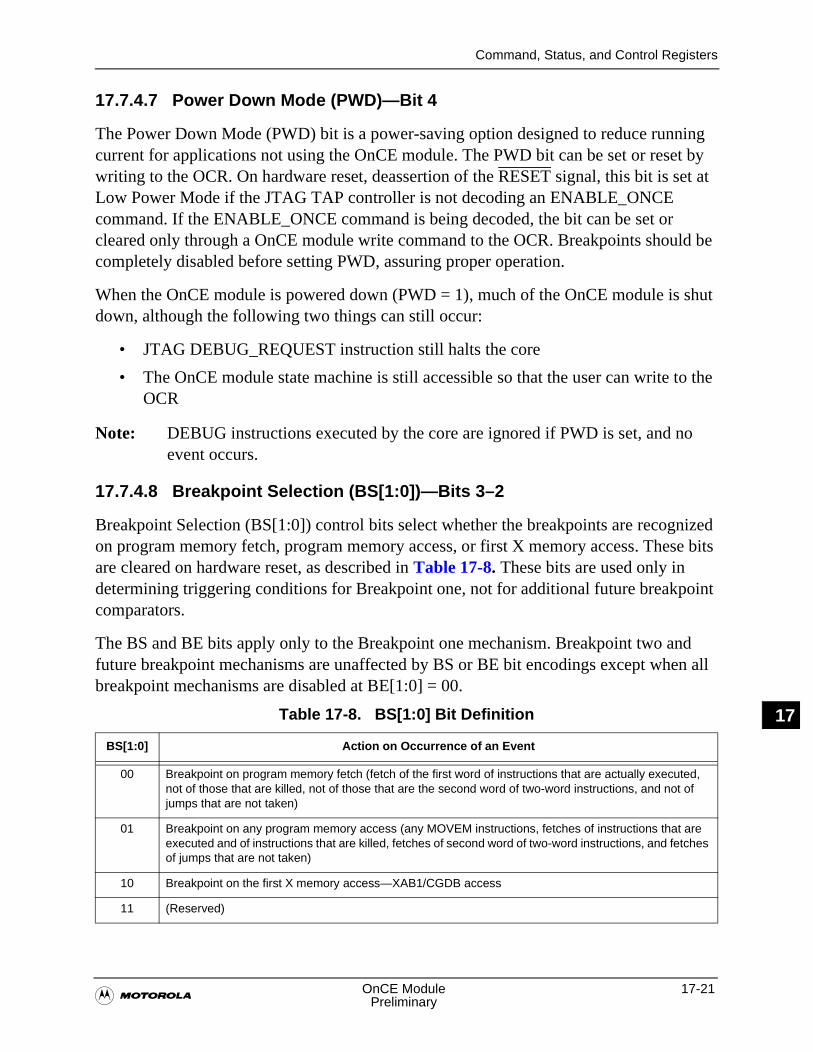
Command, Status, and Control Registers
�OnCE Module 17-21
Preliminary
N17
17.7.4.7 Power Down Mode (PWD)—Bit 4
The Power Down Mode (PWD) bit is a power-saving option designed to reduce running current for applications not using the OnCE module. The PWD bit can be set or reset by writing to the OCR. On hardware reset, deassertion of the RESET signal, this bit is set at Low Power Mode if the JTAG TAP controller is not decoding an ENABLE_ONCE command. If the ENABLE_ONCE command is being decoded, the bit can be set or cleared only through a OnCE module write command to the OCR. Breakpoints should be completely disabled before setting PWD, assuring proper operation.
When the OnCE module is powered down (PWD = 1), much of the OnCE module is shut down, although the following two things can still occur:
• JTAG DEBUG_REQUEST instruction still halts the core
• The OnCE module state machine is still accessible so that the user can write to the OCR
Note: DEBUG instructions executed by the core are ignored if PWD is set, and no event occurs.
17.7.4.8 Breakpoint Selection (BS[1:0])—Bits 3–2
Breakpoint Selection (BS[1:0]) control bits select whether the breakpoints are recognized on program memory fetch, program memory access, or first X memory access. These bits are cleared on hardware reset, as described in Table 17-8. These bits are used only in determining triggering conditions for Breakpoint one, not for additional future breakpoint comparators.
The BS and BE bits apply only to the Breakpoint one mechanism. Breakpoint two and future breakpoint mechanisms are unaffected by BS or BE bit encodings except when all breakpoint mechanisms are disabled at BE[1:0] = 00.
Table 17-8. BS[1:0] Bit Definition
BS[1:0] Action on Occurrence of an Event
00 Breakpoint on program memory fetch (fetch of the first word of instructions that are actually executed, not of those that are killed, not of those that are the second word of two-word instructions, and not of jumps that are not taken)
01 Breakpoint on any program memory access (any MOVEM instructions, fetches of instructions that are executed and of instructions that are killed, fetches of second word of two-word instructions, and fetches of jumps that are not taken)
10 Breakpoint on the first X memory access—XAB1/CGDB access
11 (Reserved)
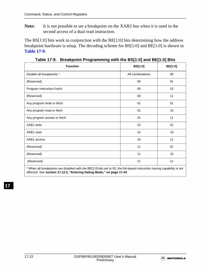
17-22 DSP56F801/803/805/807 User’s Manual�Preliminary
Command, Status, and Control Registers
N17
Note: It is not possible to set a breakpoint on the XAB2 bus when it is used in the second access of a dual read instruction.
The BS[1:0] bits work in conjunction with the BE[1:0] bits determining how the address breakpoint hardware is setup. The decoding scheme for BS[1:0] and BE[1:0] is shown in Table 17-9.
Table 17-9. Breakpoint Programming with the BS[1:0] and BE[1:0] Bits
Function BS[1:0] BE[1:0]
Disable all breakpoints * All combinations 00
(Reserved) 00 01
Program Instruction Fetch 00 10
(Reserved) 00 11
Any program write or fetch 01 01
Any program read or fetch 01 10
Any program access or fetch 01 11
XAB1 write 10 01
XAB1 read 10 10
XAB1 access 10 11
(Reserved) 11 01
(Reserved) 11 10
(Reserved) 11 11
* When all breakpoints are disabled with the BE[1:0] bits set to 00, the full-speed instruction tracing capability is not affected. See section 17.12.2, “Entering Debug Mode,” on page 17-44 .
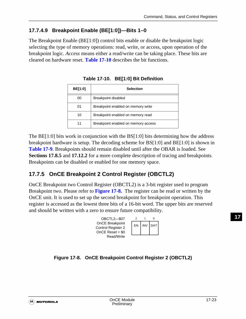
Command, Status, and Control Registers
�OnCE Module 17-23
Preliminary
N17
17.7.4.9 Breakpoint Enable (BE[1:0])—Bits 1–0
The Breakpoint Enable (BE[1:0]) control bits enable or disable the breakpoint logic selecting the type of memory operations: read, write, or access, upon operation of the breakpoint logic. Access means either a read/write can be taking place. These bits are cleared on hardware reset. Table 17-10 describes the bit functions.
The BE[1:0] bits work in conjunction with the BS[1:0] bits determining how the address breakpoint hardware is setup. The decoding scheme for BS[1:0] and BE[1:0] is shown in Table 17-9. Breakpoints should remain disabled until after the OBAR is loaded. See Sections 17.8.5 and 17.12.2 for a more complete description of tracing and breakpoints.
Breakpoints can be disabled or enabled for one memory space.
17.7.5 OnCE Breakpoint 2 Control Register (OBCTL2)
OnCE Breakpoint two Control Register (OBCTL2) is a 3-bit register used to program Breakpoint two. Please refer to Figure 17-8. The register can be read or written by the OnCE unit. It is used to set up the second breakpoint for breakpoint operation. This register is accessed as the lowest three bits of a 16-bit word. The upper bits are reserved and should be written with a zero to ensure future compatibility.
Figure 17-8. OnCE Breakpoint Control Register 2 (OBCTL2)
Table 17-10. BE[1:0] Bit Definition
BE[1:0] Selection
00 Breakpoint disabled
01 Breakpoint enabled on memory write
10 Breakpoint enabled on memory read
11 Breakpoint enabled on memory access
OBCTL2—$07OnCE Breakpoint
Control Register 2OnCE Reset = $0
Read/Write
EN INV DAT
2 1 0
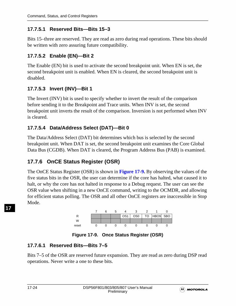
17-24 DSP56F801/803/805/807 User’s Manual�Preliminary
Command, Status, and Control Registers
N17
17.7.5.1 Reserved Bits—Bits 15–3
Bits 15–three are reserved. They are read as zero during read operations. These bits should be written with zero assuring future compatibility.
17.7.5.2 Enable (EN)—Bit 2
The Enable (EN) bit is used to activate the second breakpoint unit. When EN is set, the second breakpoint unit is enabled. When EN is cleared, the second breakpoint unit is disabled.
17.7.5.3 Invert (INV)—Bit 1
The Invert (INV) bit is used to specify whether to invert the result of the comparison before sending it to the Breakpoint and Trace units. When INV is set, the second breakpoint unit inverts the result of the comparison. Inversion is not performed when INV is cleared.
17.7.5.4 Data/Address Select (DAT)—Bit 0
The Data/Address Select (DAT) bit determines which bus is selected by the second breakpoint unit. When DAT is set, the second breakpoint unit examines the Core Global Data Bus (CGDB). When DAT is cleared, the Program Address Bus (PAB) is examined.
17.7.6 OnCE Status Register (OSR)
The OnCE Status Register (OSR) is shown in Figure 17-9. By observing the values of the five status bits in the OSR, the user can determine if the core has halted, what caused it to halt, or why the core has not halted in response to a Debug request. The user can see the OSR value when shifting in a new OnCE command, writing to the OCMDR, and allowing for efficient status polling. The OSR and all other OnCE registers are inaccessible in Stop Mode.
17.7.6.1 Reserved Bits—Bits 7–5
Bits 7–5 of the OSR are reserved future expansion. They are read as zero during DSP read operations. Never write a one to these bits.
7 6 5 4 3 2 1 0
R OS1 OS0 TO HBO9 SBO
W
reset 0 0 0 0 0 0 0 0
Figure 17-9. Once Status Register (OSR)
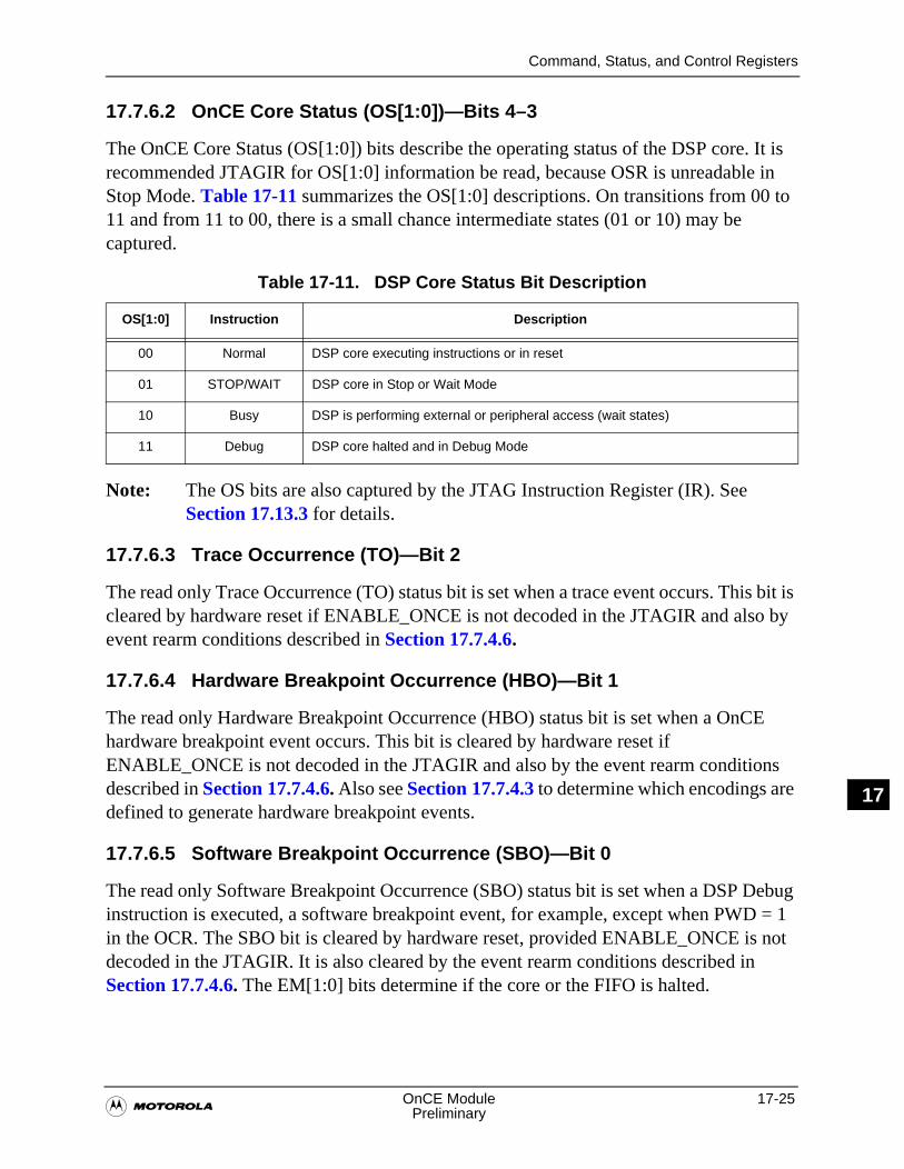
Command, Status, and Control Registers
�OnCE Module 17-25
Preliminary
N17
17.7.6.2 OnCE Core Status (OS[1:0])—Bits 4–3
The OnCE Core Status (OS[1:0]) bits describe the operating status of the DSP core. It is recommended JTAGIR for OS[1:0] information be read, because OSR is unreadable in Stop Mode. Table 17-11 summarizes the OS[1:0] descriptions. On transitions from 00 to 11 and from 11 to 00, there is a small chance intermediate states (01 or 10) may be captured.
Note: The OS bits are also captured by the JTAG Instruction Register (IR). See Section 17.13.3 for details.
17.7.6.3 Trace Occurrence (TO)—Bit 2
The read only Trace Occurrence (TO) status bit is set when a trace event occurs. This bit is cleared by hardware reset if ENABLE_ONCE is not decoded in the JTAGIR and also by event rearm conditions described in Section 17.7.4.6.
17.7.6.4 Hardware Breakpoint Occurrence (HBO)—Bit 1
The read only Hardware Breakpoint Occurrence (HBO) status bit is set when a OnCE hardware breakpoint event occurs. This bit is cleared by hardware reset if ENABLE_ONCE is not decoded in the JTAGIR and also by the event rearm conditions described in Section 17.7.4.6. Also see Section 17.7.4.3 to determine which encodings are defined to generate hardware breakpoint events.
17.7.6.5 Software Breakpoint Occurrence (SBO)—Bit 0
The read only Software Breakpoint Occurrence (SBO) status bit is set when a DSP Debug instruction is executed, a software breakpoint event, for example, except when PWD = 1 in the OCR. The SBO bit is cleared by hardware reset, provided ENABLE_ONCE is not decoded in the JTAGIR. It is also cleared by the event rearm conditions described in Section 17.7.4.6. The EM[1:0] bits determine if the core or the FIFO is halted.
Table 17-11. DSP Core Status Bit Description
OS[1:0] Instruction Description
00 Normal DSP core executing instructions or in reset
01 STOP/WAIT DSP core in Stop or Wait Mode
10 Busy DSP is performing external or peripheral access (wait states)
11 Debug DSP core halted and in Debug Mode
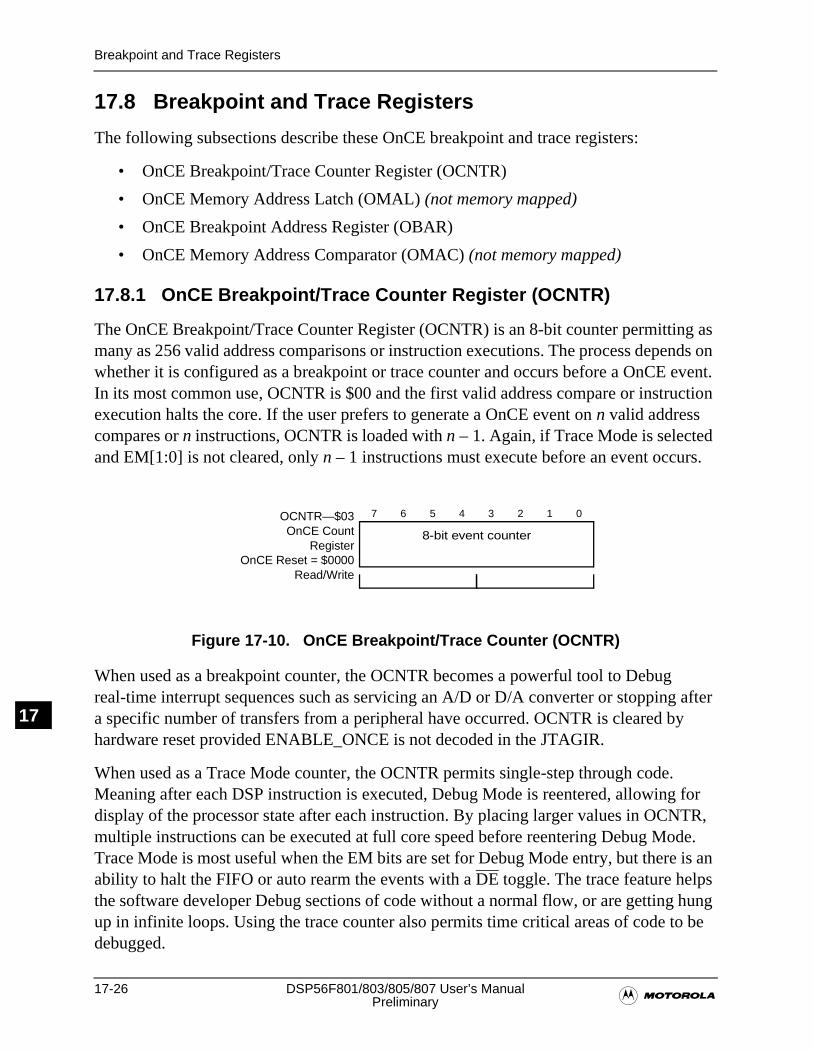
17-26 DSP56F801/803/805/807 User’s Manual�Preliminary
Breakpoint and Trace Registers
N17
17.8 Breakpoint and Trace Registers
The following subsections describe these OnCE breakpoint and trace registers:
• OnCE Breakpoint/Trace Counter Register (OCNTR)
• OnCE Memory Address Latch (OMAL) (not memory mapped)
• OnCE Breakpoint Address Register (OBAR)
• OnCE Memory Address Comparator (OMAC) (not memory mapped)
17.8.1 OnCE Breakpoint/Trace Counter Register (OCNTR)
The OnCE Breakpoint/Trace Counter Register (OCNTR) is an 8-bit counter permitting as many as 256 valid address comparisons or instruction executions. The process depends on whether it is configured as a breakpoint or trace counter and occurs before a OnCE event. In its most common use, OCNTR is $00 and the first valid address compare or instruction execution halts the core. If the user prefers to generate a OnCE event on n valid address compares or n instructions, OCNTR is loaded with n – 1. Again, if Trace Mode is selected and EM[1:0] is not cleared, only n – 1 instructions must execute before an event occurs.
Figure 17-10. OnCE Breakpoint/Trace Counter (OCNTR)
When used as a breakpoint counter, the OCNTR becomes a powerful tool to Debug real-time interrupt sequences such as servicing an A/D or D/A converter or stopping after a specific number of transfers from a peripheral have occurred. OCNTR is cleared by hardware reset provided ENABLE_ONCE is not decoded in the JTAGIR.
When used as a Trace Mode counter, the OCNTR permits single-step through code. Meaning after each DSP instruction is executed, Debug Mode is reentered, allowing for display of the processor state after each instruction. By placing larger values in OCNTR, multiple instructions can be executed at full core speed before reentering Debug Mode. Trace Mode is most useful when the EM bits are set for Debug Mode entry, but there is an ability to halt the FIFO or auto rearm the events with a DE toggle. The trace feature helps the software developer Debug sections of code without a normal flow, or are getting hung up in infinite loops. Using the trace counter also permits time critical areas of code to be debugged.
OCNTR—$03OnCE Count
RegisterOnCE Reset = $0000
Read/Write
8-bit event counter
7 6 5 4 3 2 1 0
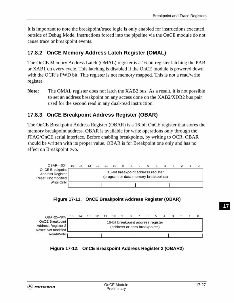
Breakpoint and Trace Registers
�OnCE Module 17-27
Preliminary
N17
It is important to note the breakpoint/trace logic is only enabled for instructions executed outside of Debug Mode. Instructions forced into the pipeline via the OnCE module do not cause trace or breakpoint events.
17.8.2 OnCE Memory Address Latch Register (OMAL)
The OnCE Memory Address Latch (OMAL) register is a 16-bit register latching the PAB or XAB1 on every cycle. This latching is disabled if the OnCE module is powered down with the OCR’s PWD bit. This register is not memory mapped. This is not a read/write register.
Note: The OMAL register does not latch the XAB2 bus. As a result, it is not possible to set an address breakpoint on any access done on the XAB2/XDB2 bus pair used for the second read in any dual-read instruction.
17.8.3 OnCE Breakpoint Address Register (OBAR)
The OnCE Breakpoint Address Register (OBAR) is a 16-bit OnCE register that stores the memory breakpoint address. OBAR is available for write operations only through the JTAG/OnCE serial interface. Before enabling breakpoints, by writing to OCR, OBAR should be written with its proper value. OBAR is for Breakpoint one only and has no effect on Breakpoint two.
Figure 17-11. OnCE Breakpoint Address Register (OBAR)
Figure 17-12. OnCE Breakpoint Address Register 2 (OBAR2)
OBAR—$04OnCE BreakpointAddress Register
Reset: Not modifiedWrite Only
16-bit breakpoint address register(program or data memory breakpoints)
11 10 9 8 7 6 5 4 3 2 1 015 14 13 12
OBAR2—$05OnCE Breakpoint
Address Register 2Reset: Not modified
Read/Write
16-bit breakpoint address register(address or data breakpoints)
11 10 9 8 7 6 5 4 3 2 1 015 14 13 12
17-28 DSP56F801/803/805/807 User’s Manual�Preliminary
Breakpoint and Trace Registers
N17
17.8.4 OnCE Memory Address Comparator (OMAC)
The OnCE Memory Address Comparator (OMAC) is a 16-bit comparator that compares the current memory address (stored by OMAL) with memory address register (OBAR). If OMAC is equal to OMAL, then the comparator delivers a signal indicating that the breakpoint address has been reached. This register is not memory mapped. It is not a read/write register.
17.8.5 OnCE Breakpoint and Trace Section
Two capabilities useful for real-time debugging of embedded control applications are address breakpoints and full-speed instruction tracing. Traditionally, processors had set a breakpoint in program memory by replacing the instruction at the breakpoint address with an illegal instruction causing a breakpoint exception. This technique is limiting because breakpoints can only be set in RAM at the beginning of an opcode and not on an operand. Additionally, this technique does not permit breakpoints to be set on data memory locations. The DSP56F801/803/805/807 instead provides on-chip address comparison hardware for setting breakpoints on program or data memory accesses. This grants breakpoints to be set on Program ROM as well as Program RAM locations. Breakpoints can be programmed for reads, writes, program fetches, or memory accesses using the OCR’s BS and BE bits. See Section 17.7.4.8.
The breakpoint logic can be enabled for the following:
• Program instruction fetches
• Program memory accesses via the MOVE(M) instruction (read, write, or access)
• X data memory accesses (read, write, or access)
• On-chip peripheral register accesses (read, write, or access)
• On either of two program memory breakpoints (i.e., on either of two instructions)
• On a single bit or field of bits in a data value at a particular address in data memory
• On a program memory or data memory location (on XAB1)
• On a sequence of two breakpoints
Breakpoints are also possible during on-chip peripheral register accesses because these are implemented as memory-mapped registers in the X data space.
In addition, the DSP56F801/803/805/807 OnCE module provides a full-speed tracing capability, the capability to execute as many as 256 instructions at full speed before reentering the Debug processing state, or simply generate a OnCE event. This permits a single-step program in the simplest case, when the counter is set for one occurrence or to execute many instructions at full speed before returning to the Debug Mode.
Pipeline Registers
�OnCE Module 17-29
Preliminary
N17
Breakpoint logic and trace logic have been designed to work together making it possible to set up more sophisticated trigger conditions and combining as many as two breakpoints and trace logic. Individual events and conditions leading to triggering can also be modified.
While debugging, sometimes not enough breakpoints are available. In this case, the core-based Debug instruction can be substituted for the desired breakpoint location. The JTAG instruction DEBUG_REQUEST (0111) can be used to force the Debug Mode.
17.9 Pipeline Registers
The OnCE module provides a halt capability of the DSP core on any instruction boundary. Upon halting the core, instructions can be executed from the Debug Mode, giving access to on-chip memory and registers. These register values can be brought out through the OnCE module by executing a sequence of DSP instructions moving values to Peripheral Global Data Bus (PGDB) and followed by OnCE commands to read the OPGDBR. This register is detailed in Section 17.9.6.
Executing instructions from the Debug Mode destroys the pipeline information. The OnCE module provides a means to preserve the pipeline when entering the Debug Mode and restoring it while leaving the Debug Mode.
A restricted set of one- and two-word instructions can be executed from Debug Mode. Three-word instructions cannot be forced into the pipeline. But the pipeline can be restored regardless of whether the next instruction to be executed is one, two, or three words long.
The OnCE module provides the following pipeline registers:
• OnCE PAB Fetch Register (OPABFR)
• OnCE PAB Decode Register (OPABDR)
• OnCE PAB Execute Register (OPABER)
• OnCE PGDB Register (OPDBR)
• OnCE PGDB Register (OPGDBR)
• OnCE PAB Change-of-Flow FIFO Register (OPFIFO) (not memory mapped)
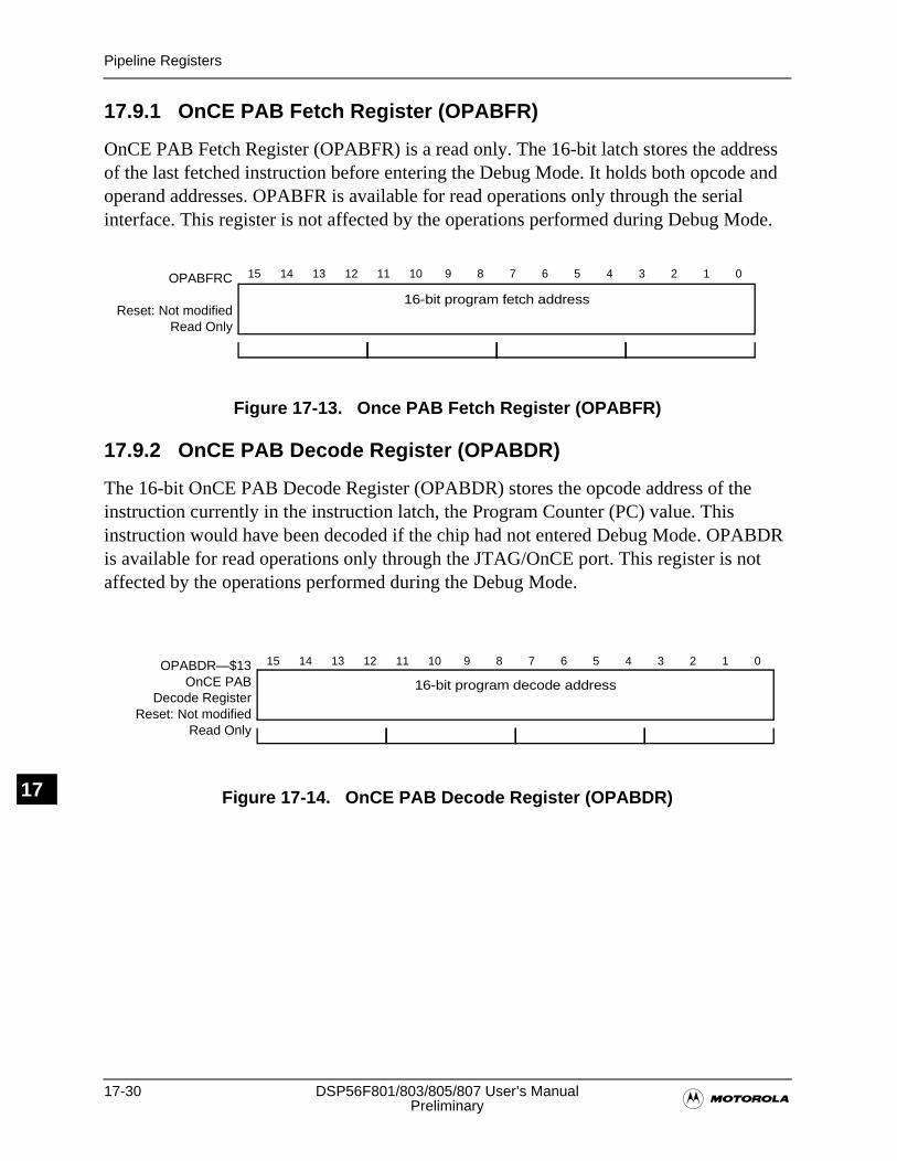
17-30 DSP56F801/803/805/807 User’s Manual�Preliminary
Pipeline Registers
N17
17.9.1 OnCE PAB Fetch Register (OPABFR)
OnCE PAB Fetch Register (OPABFR) is a read only. The 16-bit latch stores the address of the last fetched instruction before entering the Debug Mode. It holds both opcode and operand addresses. OPABFR is available for read operations only through the serial interface. This register is not affected by the operations performed during Debug Mode.
Figure 17-13. Once PAB Fetch Register (OPABFR)
17.9.2 OnCE PAB Decode Register (OPABDR)
The 16-bit OnCE PAB Decode Register (OPABDR) stores the opcode address of the instruction currently in the instruction latch, the Program Counter (PC) value. This instruction would have been decoded if the chip had not entered Debug Mode. OPABDR is available for read operations only through the JTAG/OnCE port. This register is not affected by the operations performed during the Debug Mode.
Figure 17-14. OnCE PAB Decode Register (OPABDR)
OPABFRC
Reset: Not modifiedRead Only
16-bit program fetch address
11 10 9 8 7 6 5 4 3 2 1 015 14 13 12
OPABDR—$13OnCE PAB
Decode RegisterReset: Not modified
Read Only
16-bit program decode address
11 10 9 8 7 6 5 4 3 2 1 015 14 13 12

Pipeline Registers
�OnCE Module 17-31
Preliminary
N17
17.9.3 OnCE PAB Execute Register (OPABER)
The 16-bit OnCE PAB Execute Register (OPABER) stores the opcode address of the last instruction executed before entering Debug Mode. OPABER is available for read operations only through the JTAG/OnCE port. This register is not affected by operations performed during the Debug Mode.
Figure 17-15. OnCE PAB Execute Register (OPABER)
17.9.4 OnCE PAB Change-of-Flow FIFO (OPFIFO)
The OnCE PAB Change-of-Flow FIFO (OPFIFO) register consists of multiple 16-bit register locations, though all locations are accessed through the same address as RS[4:0] in the OCMDR. The registers are serially available for read to the command controller through their common OPFIFO address. The OPFIFO is not affected by the operations performed during the Debug Mode, except for the shifting performed after reading an OPFIFO value. This register is not memory mapped and bits cannot be written to or read.
17.9.5 OnCE PDB Register (OPDBR)
The OnCE PDB (OPDBR) is a read/write register, 16-bit latch capable of storing the value of the Program Data Bus (PDB). The PDB is generated by the last program memory access of the DSP before the Debug Mode is entered. OPDBR is available only for read/write operations through the JTAG/OnCE serial interface and only when the chip is in the Debug Mode. Any attempted read of OPDBR when the chip is not in the Debug Mode results in the JTAG shifter capturing and shifting unspecified data. Similarly, any attempted write has no effect.
Figure 17-16. OnCE PDB Register (OPDBR)
OPABER—$10OnCE PAB
Execute RegisterReset: Not modified
Read Only
16-bit program execute address
11 10 9 8 7 6 5 4 3 2 1 015 14 13 12
OPDBR—$09OnCE PDB
RegisterReset: Not modified
Read/Write
16-bit register used to execute instructions in Debug Modeand restore pipeline upon exit
11 10 9 8 7 6 5 4 3 2 1 015 14 13 12

17-32 DSP56F801/803/805/807 User’s Manual�Preliminary
Pipeline Registers
N17
Immediately upon entering the Debug Mode, OPDBR should be read out via a OnCE command by selecting OPDBR for read. This value must then be saved externally if the pipeline is to be restored, as is typically the case. Any OPGDBR access corrupts PDB, so if OPDBR is to be saved, it must be saved before OPGDBR read/writes.
To restore the pipeline, regardless where the Debug Mode was entered in the instruction flow, the same sequence must take place.
• First, the value read out of OPBDR upon entry to the Debug Mode is written back to OPDBR with GO = EX = 0
• Next, that same value is written again to OPDBR, but this time with GO = EX = 1
The first write is necessary to restore PAB. The old PAB value is saved in the FIFO and restored on the first write. It is not restored directly by the user. The second write actually restores OPDBR and the GO = EX = 1 restarts the core.
To force execution of a one-word instruction from the Debug Mode, write the OPDBR with the opcode of the instruction to be executed and set GO = 1 and EX = 0. The instruction then implements while executing, OS[1:0] = 00. Upon completion, OS[1:0] = 11, the Debug Mode. Poll JTAGIR to determine if the instruction has completed. The period of time OS[1:0] = 00 is typically unnoticeably small. By the time JTAGIR polls status and is read, OS[1:0] = 11. The only time this is not true is on chips with mechanisms extending wait states infinitely, for example: transfer acknowledge pins. In that case, polling is necessary. Only a restricted set of one-word instructions can be executed from the Debug Mode.
To force execution of a two-word instruction from Debug Mode, write the OPDBR with the opcode of the instruction to be executed and set GO = EX = 0. Next, write OPDBR with the operand with GO = 1 and EX = 0. The instruction then executes. As in the one-word case, JTAGIR should be polled for status. Only a restricted set of two-word instructions can be executed from the Debug Mode.
The set of supported instructions for execution from the Debug Mode, GO but not EX are:
• JMP #xxxx
• MOVE #xxxx,register
• MOVE register,x:$ffff
• MOVE register,register
• MOVE register,x:(r0)+
• MOVE x:(r0)+,register
• MOVE register,p:(r0)+
• MOVE p:(r0)+,register
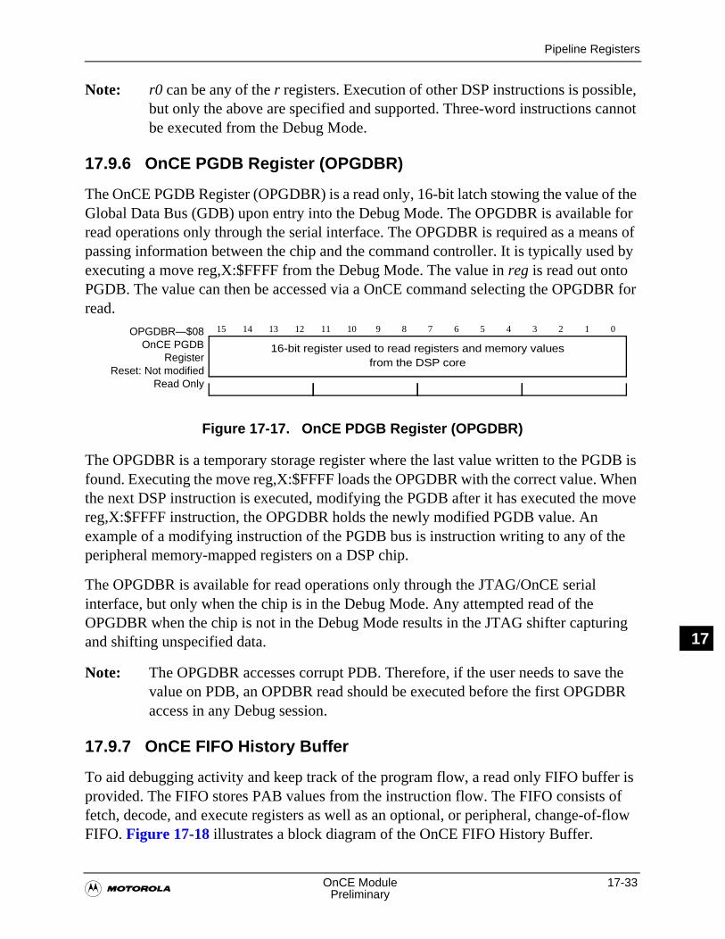
Pipeline Registers
�OnCE Module 17-33
Preliminary
N17
Note: r0 can be any of the r registers. Execution of other DSP instructions is possible, but only the above are specified and supported. Three-word instructions cannot be executed from the Debug Mode.
17.9.6 OnCE PGDB Register (OPGDBR)
The OnCE PGDB Register (OPGDBR) is a read only, 16-bit latch stowing the value of the Global Data Bus (GDB) upon entry into the Debug Mode. The OPGDBR is available for read operations only through the serial interface. The OPGDBR is required as a means of passing information between the chip and the command controller. It is typically used by executing a move reg,X:$FFFF from the Debug Mode. The value in reg is read out onto PGDB. The value can then be accessed via a OnCE command selecting the OPGDBR for read.
Figure 17-17. OnCE PDGB Register (OPGDBR)
The OPGDBR is a temporary storage register where the last value written to the PGDB is found. Executing the move reg,X:$FFFF loads the OPGDBR with the correct value. When the next DSP instruction is executed, modifying the PGDB after it has executed the move reg,X:$FFFF instruction, the OPGDBR holds the newly modified PGDB value. An example of a modifying instruction of the PGDB bus is instruction writing to any of the peripheral memory-mapped registers on a DSP chip.
The OPGDBR is available for read operations only through the JTAG/OnCE serial interface, but only when the chip is in the Debug Mode. Any attempted read of the OPGDBR when the chip is not in the Debug Mode results in the JTAG shifter capturing and shifting unspecified data.
Note: The OPGDBR accesses corrupt PDB. Therefore, if the user needs to save the value on PDB, an OPDBR read should be executed before the first OPGDBR access in any Debug session.
17.9.7 OnCE FIFO History Buffer
To aid debugging activity and keep track of the program flow, a read only FIFO buffer is provided. The FIFO stores PAB values from the instruction flow. The FIFO consists of fetch, decode, and execute registers as well as an optional, or peripheral, change-of-flow FIFO. Figure 17-18 illustrates a block diagram of the OnCE FIFO History Buffer.
OPGDBR—$08OnCE PGDB
RegisterReset: Not modified
Read Only
16-bit register used to read registers and memory valuesfrom the DSP core
11 10 9 8 7 6 5 4 3 2 1 015 14 13 12
17-34 DSP56F801/803/805/807 User’s Manual�Preliminary
Pipeline Registers
N17
The following instructions are considered to be change-of-flow:
• BRA
• JMP
• Bcc (with condition true)
• Jcc (with condition true)
• BRSET
• BRCLR
• RTS
• RTI
• JSR
Note: Addresses of JSR instructions at interrupt vector locations are not stored in the change-of-flow FIFO.
When one of the listed instructions is executed, its opcode address is immediately placed in the top location of the Change-of-Flow FIFO, as well as being placed in OPABER. Previous addresses placed in the OPFIFO are shifted down one location and the oldest address is overwritten. The OPABDR holds the PC value. If the core has been halted, the next opcode to be executed resides at the memory location pointed to by OPABDR.
Reads of the OPFIFO register return the oldest value in the OPFIFO first. The next read returns the next oldest. The nth read in an n-deep OPFIFO returns the latest change-of-flow address. It is recommended all OPFIFO locations are read, for example, n reads for an n-deep OPFIFO, so the oldest-to-newest ordering is maintained when address capture resumes.
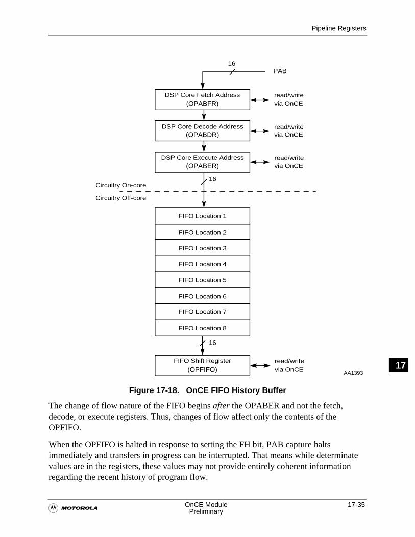
Pipeline Registers
�OnCE Module 17-35
Preliminary
N17
The change of flow nature of the FIFO begins after the OPABER and not the fetch, decode, or execute registers. Thus, changes of flow affect only the contents of the OPFIFO.
When the OPFIFO is halted in response to setting the FH bit, PAB capture halts immediately and transfers in progress can be interrupted. That means while determinate values are in the registers, these values may not provide entirely coherent information regarding the recent history of program flow.
Figure 17-18. OnCE FIFO History Buffer
PAB
DSP Core Fetch Address(OPABFR)
DSP Core Decode Address(OPABDR)
DSP Core Execute Address(OPABER)
FIFO Location 1
FIFO Location 2
FIFO Shift Register(OPFIFO)
16
16
Circuitry On-core
Circuitry Off-core
16
read/writevia OnCE
read/writevia OnCE
read/writevia OnCE
read/writevia OnCE
FIFO Location 3
FIFO Location 4
FIFO Location 5
FIFO Location 6
FIFO Location 7
FIFO Location 8
AA1393
17-36 DSP56F801/803/805/807 User’s Manual�Preliminary
Breakpoint 2 Architecture
N17
Further, the state of the OPFIFO can be different when it is halted because of an event occurring when EM = 01 than when it is halted with the core due to an event occurring when EM = 00.
17.10 Breakpoint 2 Architecture
All DSP56800 chips contain a Breakpoint one unit. The DSP56F801/803/805/807 provides a Breakpoint two unit providing greater flexibility in setting breakpoints. Adding a second breakpoint greatly increases the Debug capability of the device. It allows the following additional breakpoints to detect even more complex events:
• On either of two program memory breakpoints, such as on either of two instructions
• On a data value at a particular address in data memory
• On a bit or field of bits in a data value at a particular address in data memory
• On a program memory or data memory location (on XAB1)
• On a sequence of two breakpoints
Upon detecting a valid event, the OnCE module then performs one of the following four actions:
• Halt the DSP core and enter the Debug processing state
• Interrupt the DSP core
• Halt the OnCE FIFO, but let the DSP core continue operation
• Rearm the trigger mechanism and toggle the DE pin
The Breakpoint one unit is used in conjunction with the Breakpoint two unit for the detection of more complex trigger conditions. The Breakpoint one unit is the same as found on other DSP56800 chips. The Breakpoint two unit allows specifying more complex breakpoint conditions when used in conjunction with the first breakpoint. Additionally, it is possible to set up Breakpoint two for interrupts while leaving Breakpoint one available to the JTAG/OnCE port. Note when a breakpoint is determined the CGDB with the Breakpoint two unit, the breakpoint condition should be qualified by an X memory access with the Breakpoint one unit.
Figure 17-19 illustrates how the two breakpoint units are combined in the Breakpoint and Trace Counter Unit specifying more complex triggers to perform one of several actions upon detection of a breakpoint. In addition to simply detecting the breakpoint conditions, this unit allows the first of the two breakpoints to be qualified by the BS and BE bits found in the OCR. This allows a breakpoint to be qualified by a read/write or access condition.
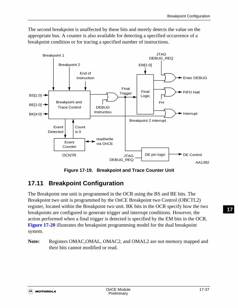
Breakpoint Configuration
�OnCE Module 17-37
Preliminary
N17
The second breakpoint is unaffected by these bits and merely detects the value on the appropriate bus. A counter is also available for detecting a specified occurrence of a breakpoint condition or for tracing a specified number of instructions.
17.11 Breakpoint Configuration
The Breakpoint one unit is programmed in the OCR using the BS and BE bits. The Breakpoint two unit is programmed by the OnCE Breakpoint two Control (OBCTL2) register, located within the Breakpoint two unit. BK bits in the OCR specify how the two breakpoints are configured to generate trigger and interrupt conditions. However, the action performed when a final trigger is detected is specified by the EM bits in the OCR. Figure 17-20 illustrates the breakpoint programming model for the dual breakpoint system.
Note: Registers OMAC,OMAL, OMAC2, and OMAL2 are not memory mapped and their bits cannot modified or read.
Figure 17-19. Breakpoint and Trace Counter Unit
BS[1:0]
OCNTR
End ofInstruction
Breakpoint and
Trace Control
EventCounter
BE[1:0]
BK[4:0]
EventDetected
Countis 0
FinalTrigger Final
Logic
EM[1:0]
DEBUGInstruction
read/writevia OnCE
Breakpoint 2
Breakpoint 1
Enter DEBUG
FIFO Halt
JTAGDEBUG_REQ
FH
Interrupt
Breakpoint 2 interrupt
DE pin logic DE ControlJTAGDEBUG_REQ
AA1392
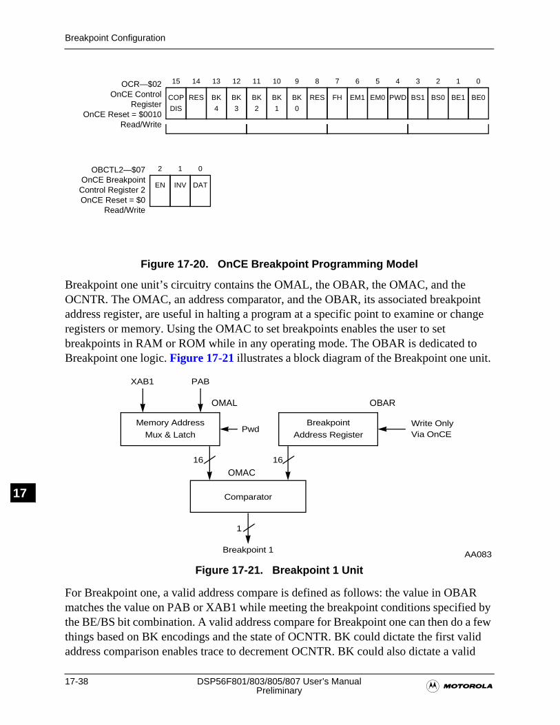
17-38 DSP56F801/803/805/807 User’s Manual�Preliminary
Breakpoint Configuration
N17
Breakpoint one unit’s circuitry contains the OMAL, the OBAR, the OMAC, and the OCNTR. The OMAC, an address comparator, and the OBAR, its associated breakpoint address register, are useful in halting a program at a specific point to examine or change registers or memory. Using the OMAC to set breakpoints enables the user to set breakpoints in RAM or ROM while in any operating mode. The OBAR is dedicated to Breakpoint one logic. Figure 17-21 illustrates a block diagram of the Breakpoint one unit.
For Breakpoint one, a valid address compare is defined as follows: the value in OBAR matches the value on PAB or XAB1 while meeting the breakpoint conditions specified by the BE/BS bit combination. A valid address compare for Breakpoint one can then do a few things based on BK encodings and the state of OCNTR. BK could dictate the first valid address comparison enables trace to decrement OCNTR. BK could also dictate a valid
Figure 17-20. OnCE Breakpoint Programming Model
Figure 17-21. Breakpoint 1 Unit
OCR—$02OnCE Control
RegisterOnCE Reset = $0010
Read/Write
BK
2
BK
1
BK
0
RES FH EM1 EM0 PWD BS1 BS0 BE1 BE0COP
DIS
RES BK
4
BK
3
11 10 9 8 7 6 5 4 3 2 1 015 14 13 12
OBCTL2—$07OnCE Breakpoint
Control Register 2OnCE Reset = $0
Read/Write
EN INV DAT
2 1 0
PABXAB1
PwdWrite Only
OMAL OBAR
OMAC
Memory Address
Mux & Latch
Breakpoint
Address Register
Comparator
Breakpoint 1
Via OnCE
16 16
1
AA083
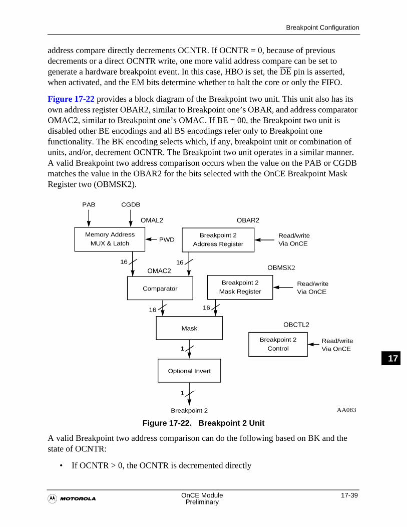
Breakpoint Configuration
�OnCE Module 17-39
Preliminary
N17
address compare directly decrements OCNTR. If OCNTR = 0, because of previous decrements or a direct OCNTR write, one more valid address compare can be set to generate a hardware breakpoint event. In this case, HBO is set, the DE pin is asserted, when activated, and the EM bits determine whether to halt the core or only the FIFO.
Figure 17-22 provides a block diagram of the Breakpoint two unit. This unit also has its own address register OBAR2, similar to Breakpoint one’s OBAR, and address comparator OMAC2, similar to Breakpoint one’s OMAC. If BE = 00, the Breakpoint two unit is disabled other BE encodings and all BS encodings refer only to Breakpoint one functionality. The BK encoding selects which, if any, breakpoint unit or combination of units, and/or, decrement OCNTR. The Breakpoint two unit operates in a similar manner. A valid Breakpoint two address comparison occurs when the value on the PAB or CGDB matches the value in the OBAR2 for the bits selected with the OnCE Breakpoint Mask Register two (OBMSK2).
A valid Breakpoint two address comparison can do the following based on BK and the state of OCNTR:
• If OCNTR > 0, the OCNTR is decremented directly
Figure 17-22. Breakpoint 2 Unit
CGDBPAB
PWDRead/write
OMAL2 OBAR2
OMAC2
Memory Address
MUX & LatchBreakpoint 2
Address Register
Comparator
Breakpoint 2
Via OnCE
Read/write
OBMSK2
Breakpoint 2
Mask Register Via OnCE
Mask
Optional Invert
Read/write
OBCTL2
Breakpoint 2
Control Via OnCE
16 16
1616
1
1
AA083
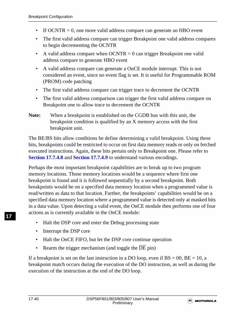
17-40 DSP56F801/803/805/807 User’s Manual�Preliminary
Breakpoint Configuration
N17
• If OCNTR = 0, one more valid address compare can generate an HBO event
• The first valid address compare can trigger Breakpoint one valid address compares to begin decrementing the OCNTR
• A valid address compare when OCNTR = 0 can trigger Breakpoint one valid address compare to generate HBO event
• A valid address compare can generate a OnCE module interrupt. This is not considered an event, since no event flag is set. It is useful for Programmable ROM (PROM) code patching
• The first valid address compare can trigger trace to decrement the OCNTR
• The first valid address comparison can trigger the first valid address compare on Breakpoint one to allow trace to decrement the OCNTR
Note: When a breakpoint is established on the CGDB bus with this unit, the breakpoint condition is qualified by an X memory access with the first breakpoint unit.
The BE/BS bits allow conditions be define determining a valid breakpoint. Using these bits, breakpoints could be restricted to occur on first data memory reads or only on fetched executed instructions. Again, these bits pertain only to Breakpoint one. Please refer to Section 17.7.4.8 and Section 17.7.4.9 to understand various encodings.
Perhaps the most important breakpoint capabilities are to break up to two program memory locations. Those memory locations would be a sequence where first one breakpoint is found and it is followed sequentially by a second breakpoint. Both breakpoints would be on a specified data memory location when a programmed value is read/written as data to that location. Further, the breakpoints’ capabilities would be on a specified data memory location where a programmed value is detected only at masked bits in a data value. Upon detecting a valid event, the OnCE module then performs one of four actions as is currently available in the OnCE module:
• Halt the DSP core and enter the Debug processing state
• Interrupt the DSP core
• Halt the OnCE FIFO, but let the DSP core continue operation
• Rearm the trigger mechanism (and toggle the DE pin)
If a breakpoint is set on the last instruction in a DO loop, even if BS = 00, BE = 10, a breakpoint match occurs during the execution of the DO instruction, as well as during the execution of the instruction at the end of the DO loop.
Breakpoint Configuration
�OnCE Module 17-41
Preliminary
N17
17.11.1 Programming the Breakpoints
Breakpoints and trace can be configured while the core is executing DSP instructions or while the core is in reset. Complete access to the breakpoint logic, OCNTR, OBAR, and OCR, is provided during these operating conditions. The chip may be held in reset, set OCNTR, OBAR, and OCR so the Debug Mode is entered on a specific condition, release reset, and Debug the application. Similarly, the application can be running while the user configures breakpoints to toggle DE on each data memory access to a certain location, thereby allowing statistical information to be gathered.
In general, to set up a breakpoint, the following sequence must be performed:
1. JTAG must be decoding ENABLE_ONCE to allow OnCE module register read/writes.
2. The PWD bit in the OCR must be cleared to power up the OnCE module, and the BE[1:0] bits in the OCR should be set to 00.
3. Write the breakpoint address into the OBAR.
4. Write n – 1 into the OCNTR, where n is the number of valid address compares required to take place before generating a OnCE event.
5. Write the OCR to set the BE, BS, and BK bits for the desired breakpoint conditions, EM to choose what happens when an event occurs, and DE to enable/disable the DE pin.
When the above steps are conducted while in the Debug Mode, exit the Debug Mode to restart the core. However, when the above steps are completed in the User Mode, the breakpoint is set immediately.
Note: OnCE events can occur even if ENABLE_ONCE is not latched in the JTAGIR. This is useful in multiprocessor applications.
The first breakpoint unit is programmed in the OCR using the BS and BE bits. The second breakpoint unit is programmed by the OnCE Breakpoint two Control (OBCTL2) register, located within the second breakpoint unit. The manner in which the two breakpoints are set up for generating triggers and interrupt conditions is specified by the BK bits in the OCR. The EM bits in the OCR specifies the action performed when a final trigger is detected.
17-42 DSP56F801/803/805/807 User’s Manual�Preliminary
Breakpoint Configuration
N17
17.11.2 . OnCE Trace Logic Operation
The trace and breakpoint logics are tightly coupled, sharing resources where necessary. When BK[4:0] = 10111, OCNTR is decremented each time an instruction is executed from Normal Mode. Instructions executed from the Debug Mode do not decrement the OCNTR. The event occurrence mechanism is slightly different for trace than for breakpoints.
For breakpoints, the event occurs when OCNTR = 0 and another valid address are compared. For trace, the event occurs, TO is set, when OCNTR first reaches zero. If the EM bits are set for entry of the Debug Mode, one more instruction is executed after TO is set. Therefore, if the user wants to halt the DSP after executing n instructions, n – 1 should be placed in OCNTR, much like the breakpoint case. But if the user would like to halt only the FIFO after n instructions, n should be placed in OCNTR. This is different from the breakpoint case and occurs because the TO flag is set when OCNTR first reaches zero. Trace events cannot cause OnCE interrupts, although TO is set and DE is asserted, pulled low, for this EM such as EM = 10 acts just like EM = 11 for trace.
Since trace events occur when OCNTR reaches zero and Trace Mode is enabled by one of the BK settings, rearming trace events responds differently than rearming breakpoint events. For example, EM = 10 and EM = 11 encodings attempt to rearm the trace event, but since the conditions are still valid for trace, TO remains set and DE remains low. Similarly, for EM = 01, FIFO halt, an OCR write attempts to clear the TO, but again the flag remains set since conditions are still valid for trace. To clear TO and capture additional FIFO values, do the following:
1. Write OCR to disable trace, FIFO begins capturing.
2. Write OCNTR with desired value.
3. Write OCR to enable trace.
4. Poll for TO = 1.
If Step one is omitted, TO is never reset and the FIFO does not begin capturing, because the conditions for valid trace are still present.
Note: There are sequential breakpoints enabling the Trace Mode. The Trace Mode operation is identical to the BK[4:0] = 10111 operation, except the HBO bit is set.
A common use of the trace logic is to execute a single instruction (OCNTR = 0), then immediately return to the Debug Mode. Upon returning to Debug Mode, the user can display registers or memory locations. When this process is repeated, the user can step through individual instructions and see their effect on the state of the processor.
The Debug Processing State
�OnCE Module 17-43
Preliminary
N17
17.12 The Debug Processing State
A DSP56800 chip in a user application can enter any of six different processing modes:
• Reset Mode
• Normal Mode
• Exception Mode
• Wait Mode
• Stop Mode
• Debug Mode
The first five of these are referenced in Chapter 7, Interrupts and the Processing States, in the DSP56800 Family Manual (DSP56800FM/AD). The last processing mode, the Debug Mode, is described in this subsection.
The Debug Mode supports the on-chip emulation features of the chip. In this mode, the DSP core is halted and set to accept OnCE commands through the JTAG port. Once the OnCE module is set up correctly, the DSP leaves the Debug Mode, returning control to the user program. The DSP reenters the Debug Mode when the previously set trigger condition occurs, provided EM = 00, OnCE events cause entry to Debug Mode.
Capabilities available in the Debug Mode include the following:
• Read and write the OnCE registers
• Read the instruction FIFO
• Reset the OnCE event counter
• Execute a single DSP instruction and return to this mode
• Execute a single DSP instruction and exit this mode
17.12.1 OnCE Normal and Debug and STOP Modes
The OnCE module has three operational modes: Normal, Debug and Stop. Whenever a STOP instruction is executed by the DSP, the OnCE module is no longer accessible. The OnCE module is in the Normal Mode except when the DSP enters the Debug Mode, or if it is in the Stop Mode. The OnCE module is in the Debug Mode whenever the DSP enters the Debug Mode. The major difference between the states is register access. The following OnCE module registers can be accessed in the Normal or Debug Modes:
• OnCE Control Register (OCR)
• OnCE Status Register (OSR)
17-44 DSP56F801/803/805/807 User’s Manual�Preliminary
The Debug Processing State
N17
• OnCE Breakpoint and Trace Counter (OCNTR)
• OnCE Breakpoint Address Register (OBAR)
• OnCE Program Address Bus Fetch Register (OPABFR) (if FIFO halted)
• OnCE PAB Decode Register (OPABDR) (if FIFO halted)
• OnCE PAB Execute Register (OPABER) (if FIFO halted)
• OnCE PAB Change-of-Flow FIFO (OPFIFO) (if FIFO halted)
The following OnCE registers can only be accessed when the module is in Debug Mode:
• OnCE Peripheral Global Data Bus Register (OPGDBR)
• OnCE Program Data Bus Register (OPDBR)
If a STOP is executed while the user is accessing OnCE in User Mode, problems may occur since few or no internal clocks are running anymore. This should be avoided. Recognize this occurrence by capturing the OS bits in the JTAGIR in Capture-IR then choose to send a DEBUG_REQUEST to bring the core out of STOP.
17.12.2 Entering Debug Mode
There are six ways to enter Debug Mode:
1. JTAG DEBUG_REQUEST during hardware reset.
2. JTAG DEBUG_REQUEST during Stop or Wait.
3. JTAG DEBUG_REQUEST during wait states.
4. Software breakpoint (DEBUG) during normal use with PWD = 0 and EM = 00.
5. Trigger events, breakpoint/Trace Modes, when EM = 00.
6. Execute a DSP instruction from Debug Mode with EX = 0.
17.12.2.1 JTAG DEBUG_REQUEST
The core reacts to a Debug request by either of these sources in the same way. To send a JTAG DEBUG_REQUEST, the 0111 opcode must be shifted into the JTAGIR, then Update-IR must be passed through. This instructs the core to halt and enter the Debug Mode. When the DSP enters the Debug Mode in response to these requests, the DE pin is asserted, or pulled low, if it is enabled.
The JTAG/OnCE interface is accessible when RESET is asserted, provided TRST is not asserted, i.e., the JTAG port is not being reset. The user can load DEBUG_REQUEST into the JTAGIR while RESET is held low. If RESET is then de disallowed, the chip exit
The Debug Processing State
�OnCE Module 17-45
Preliminary
N17
hardware reset directly into Debug Mode. After sending the DEBUG_REQUEST instruction, poll the JTAGIR to see whether the chip has entered the Debug Mode.
If the chip is in either Wait or Stop Mode, either type of Debug request brings the chip out of these modes, much like an external interrupt. Upon leaving the Wait or Stop Modes, the chip enters the Debug Mode. As always, the user should poll JTAGIR for status after sending the Debug request. It is important to remember the OSR cannot be polled during the Stop Mode because no OnCE module access is allowed. However, JTAG access is allowed.
If the chip is in wait states, because of a non-zero value in BCR or transfer acknowledge deassertion on chips having this function, the Debug request is latched and the core halts upon execution of the instruction in wait states. The period of time between Debug request and the OS bits being set to 11, the Debug Mode, is typically much shorter than the time it takes to poll status in JTAGIR, meaning OS = 11 on the first poll. The only time this is not the case is when a transfer acknowledge is generating a large or infinite number of wait states. For this reason, polling for OS = 11 is always recommended.
Sending a Debug request when the chip is in Normal Mode, results in the chip entering the Debug Mode as soon as the instruction currently executing finishes. Again, the JTAGIR should be polled for status. Please refer to Section 18.5 for information about using the JTAG TAP controller and its instructions.
17.12.2.2 Software Request During Normal Activity
Upon executing the DEBUG instruction, the chip enters the Debug processing state provided PWD = 0 and EM = 00.
17.12.2.3 Trigger Events (Breakpoint/Trace Modes)
The DSP56F801/803/805/807 allows configuration of specific trigger events. These events can include breakpoints, Trace Modes, or combinations of breakpoints and Trace Mode operations. The following conditions must occur to halt the core due to breakpoint/trace:
• EM = 00
• If OCNTR = 0, breakpoints are enabled (BE not 00), the next valid address compare causes the core to halt, provided it is not the initial enabling breakpoint in a sequential breakpoint
• If OCNTR = 0, Trace Mode is selected, one of the BK encodings with BK4 = 1, the next instruction executed causes the core to halt
17-46 DSP56F801/803/805/807 User’s Manual�Preliminary
Accessing the OnCE Module
N17
17.12.2.4 Re-entering Debug Mode with EX = 0
If a DSP instruction is executed from the Debug Mode with EX = 0, the Debug Mode is automatically entered a second time after the instruction finishes executing. When the instruction is being executed, the core is not in the Debug Mode. The OS[1:0] bits reflect this state. This change in status is typically not observable, because the core leaves and reenters the Debug Mode in a very short time. Still, polling for status in JTAGIR is recommended to guarantee the chip is in the Debug Mode.
17.12.2.5 Exiting Debug Mode
There are three ways to exit the Debug Mode:
• Restore the pipeline by writing original OPDBR value back to OPDBR twice; first with GO = EX = 0 and last with GO = EX = 1. PAB is restored from OPABFR so that fetching continues from the correct address
• Change program flow by writing jmp opcode to OPDBR with GO = EX = 0 and then writing target address to OPDBR with GO = 1, EX = 0. Next, write a NOP to OPDBR with GO = EX = 1
• Hardware reset (assertion of RESET) brings the chip out of Debug Mode provided DEBUG_REQUEST is not decoded in the JTAGI.
17.13 Accessing the OnCE Module
This subsection describes useful example sequences involving the JTAG/OnCE interface. The sequences are described in a hierarchical manner. Low-level sequences describe basic operations such as JTAG Instruction and Data Register accesses. Building on this, the second group of sequences describe more complicated sequences, For example, OnCE command entry and status polling. The final set builds further on the lower-level sequences to describe how to display core registers, set breakpoints, and change memory.
17.13.1 Primitive JTAG Sequences
The JTAG/OnCE serial protocol is identical to the protocol described in the IEEE 1149.1a-1993 Standard Test Access Port and Boundary Scan Architecture. It involves the control of four input pins: TRST, actually bidirectional, TDI, TMS and TCK, and the observance of one output pin, TDO. TDI and TDO are the serial input and output, respectively. TCK is the serial clock and TMS is an input used to selectively step through the JTAG state machine. TRST is an asynchronous reset of the JTAG port.
The following descriptions refer to states in the JTAG state machine diagram described in Figure 18-8. Please refer to this diagram or to the IEEE 1149.1a-1993 document.
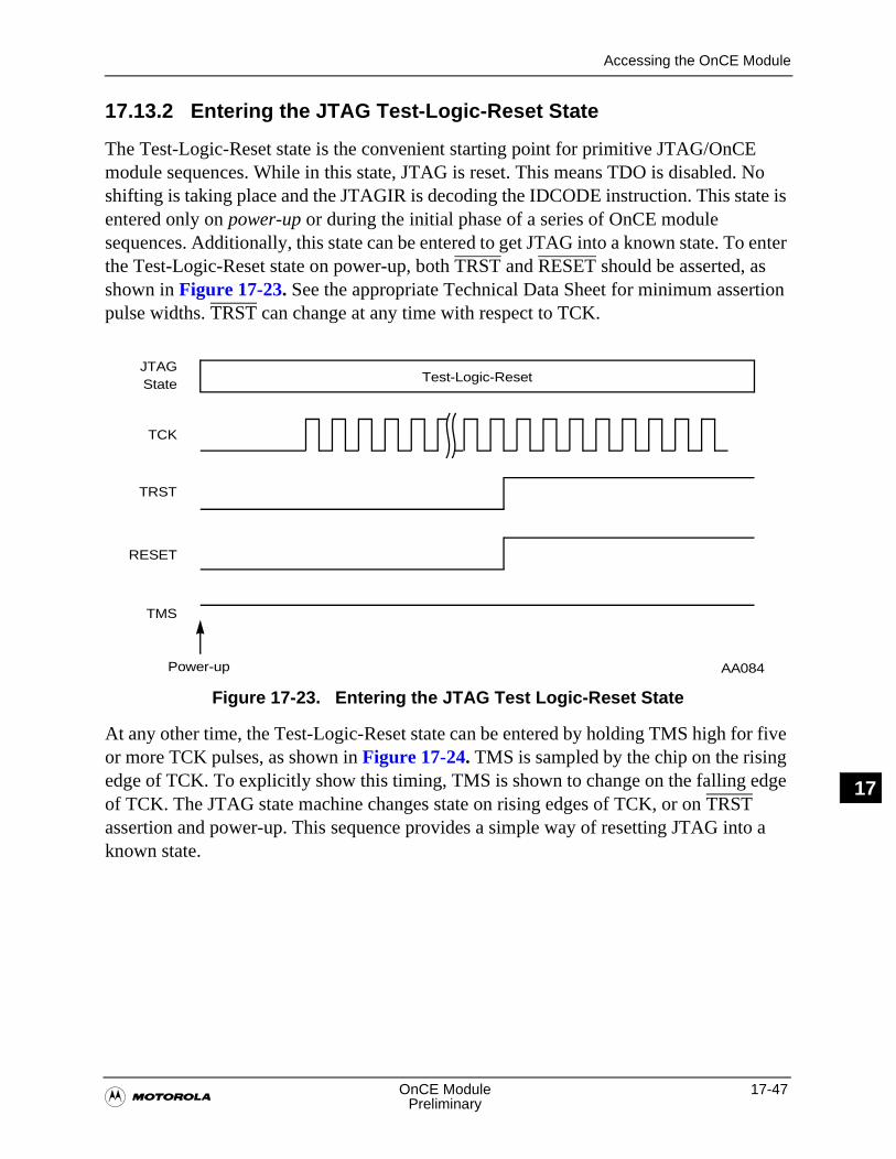
Accessing the OnCE Module
�OnCE Module 17-47
Preliminary
N17
17.13.2 Entering the JTAG Test-Logic-Reset State
The Test-Logic-Reset state is the convenient starting point for primitive JTAG/OnCE module sequences. While in this state, JTAG is reset. This means TDO is disabled. No shifting is taking place and the JTAGIR is decoding the IDCODE instruction. This state is entered only on power-up or during the initial phase of a series of OnCE module sequences. Additionally, this state can be entered to get JTAG into a known state. To enter the Test-Logic-Reset state on power-up, both TRST and RESET should be asserted, as shown in Figure 17-23. See the appropriate Technical Data Sheet for minimum assertion pulse widths. TRST can change at any time with respect to TCK.
At any other time, the Test-Logic-Reset state can be entered by holding TMS high for five or more TCK pulses, as shown in Figure 17-24. TMS is sampled by the chip on the rising edge of TCK. To explicitly show this timing, TMS is shown to change on the falling edge of TCK. The JTAG state machine changes state on rising edges of TCK, or on TRST assertion and power-up. This sequence provides a simple way of resetting JTAG into a known state.
Figure 17-23. Entering the JTAG Test Logic-Reset State
JTAGState
TCK
TRST
RESET
TMS
Test-Logic-Reset
Power-up AA084
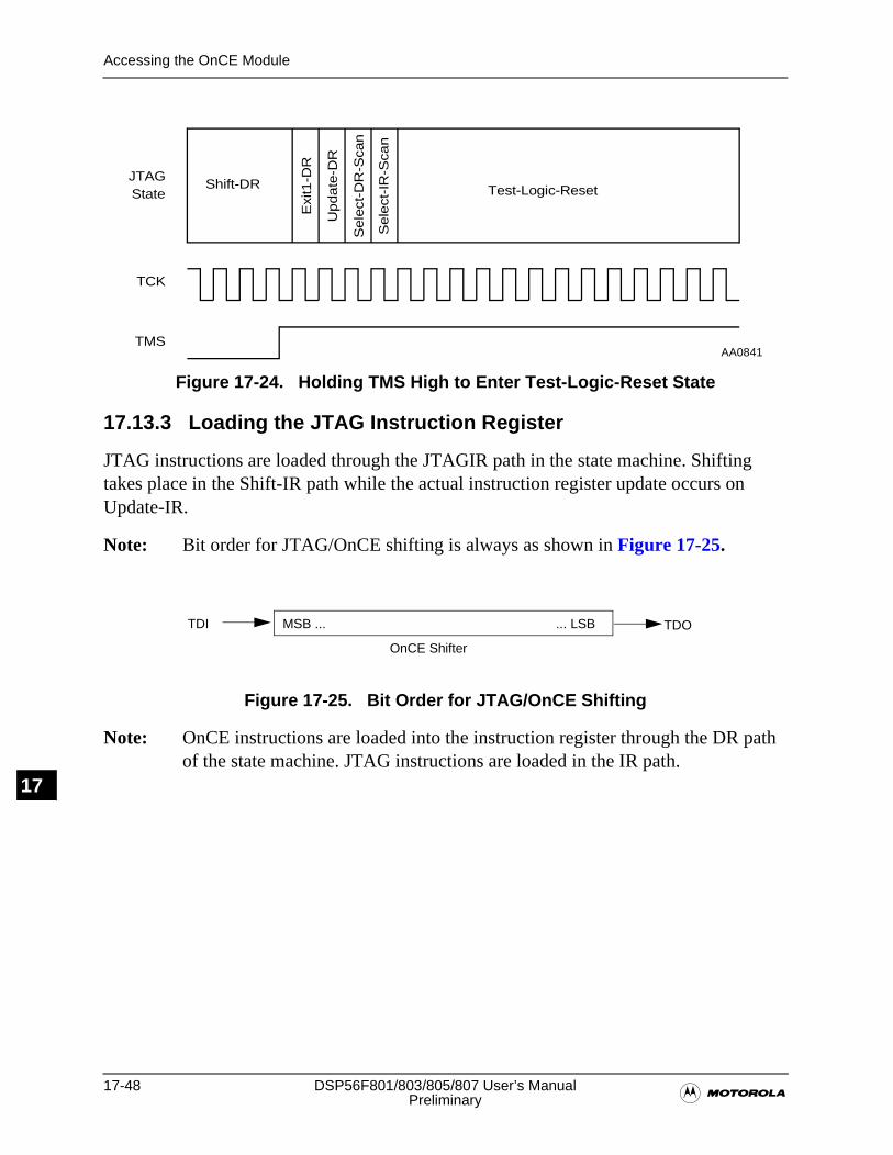
17-48 DSP56F801/803/805/807 User’s Manual�Preliminary
Accessing the OnCE Module
N17
17.13.3 Loading the JTAG Instruction Register
JTAG instructions are loaded through the JTAGIR path in the state machine. Shifting takes place in the Shift-IR path while the actual instruction register update occurs on Update-IR.
Note: Bit order for JTAG/OnCE shifting is always as shown in Figure 17-25.
Note: OnCE instructions are loaded into the instruction register through the DR path of the state machine. JTAG instructions are loaded in the IR path.
Figure 17-24. Holding TMS High to Enter Test-Logic-Reset State
Figure 17-25. Bit Order for JTAG/OnCE Shifting
JTAGState
TCK
TMS
Shift-DR
Sele
ct-D
R-S
can
Update
-DR
Exi
t1-D
R
Sele
ct-I
R-S
can
Test-Logic-Reset
AA0841
TDOTDI
OnCE Shifter
MSB ... ... LSB
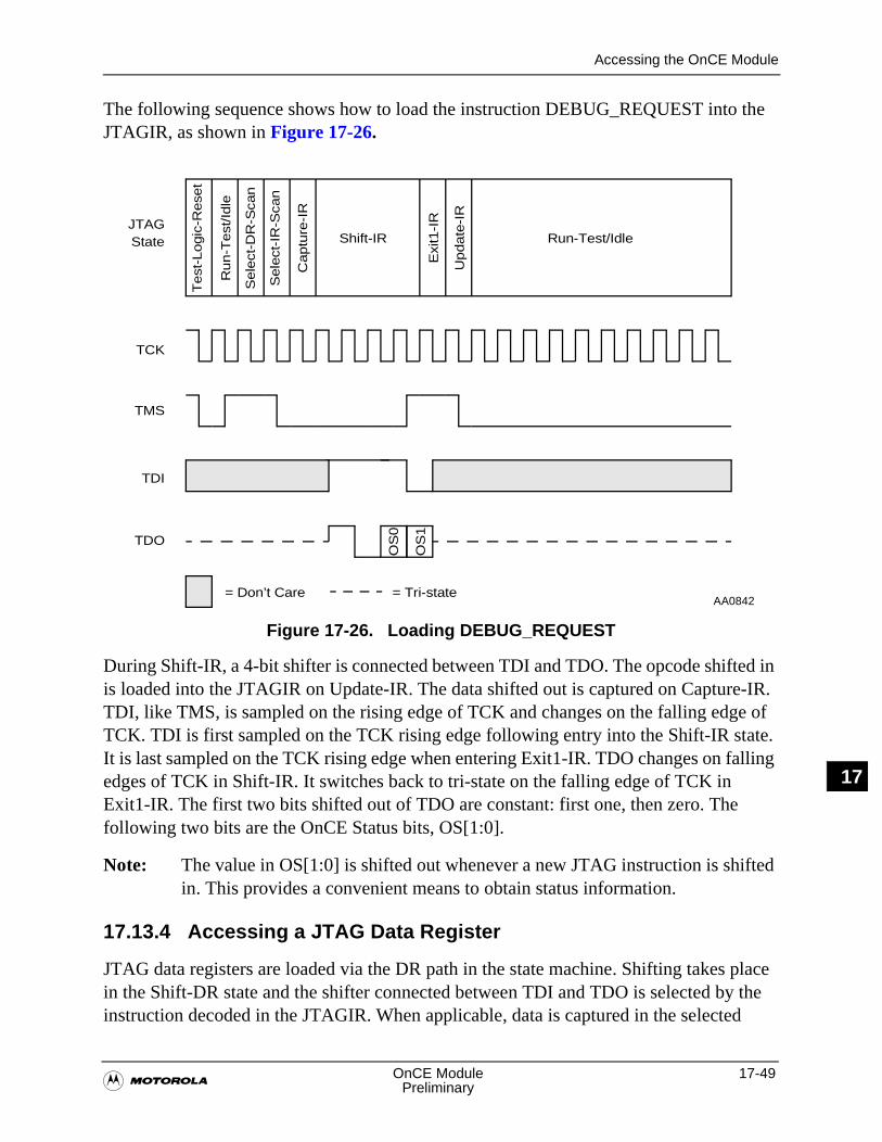
Accessing the OnCE Module
�OnCE Module 17-49
Preliminary
N17
The following sequence shows how to load the instruction DEBUG_REQUEST into the JTAGIR, as shown in Figure 17-26.
During Shift-IR, a 4-bit shifter is connected between TDI and TDO. The opcode shifted in is loaded into the JTAGIR on Update-IR. The data shifted out is captured on Capture-IR. TDI, like TMS, is sampled on the rising edge of TCK and changes on the falling edge of TCK. TDI is first sampled on the TCK rising edge following entry into the Shift-IR state. It is last sampled on the TCK rising edge when entering Exit1-IR. TDO changes on falling edges of TCK in Shift-IR. It switches back to tri-state on the falling edge of TCK in Exit1-IR. The first two bits shifted out of TDO are constant: first one, then zero. The following two bits are the OnCE Status bits, OS[1:0].
Note: The value in OS[1:0] is shifted out whenever a new JTAG instruction is shifted in. This provides a convenient means to obtain status information.
17.13.4 Accessing a JTAG Data Register
JTAG data registers are loaded via the DR path in the state machine. Shifting takes place in the Shift-DR state and the shifter connected between TDI and TDO is selected by the instruction decoded in the JTAGIR. When applicable, data is captured in the selected
Figure 17-26. Loading DEBUG_REQUEST
JTAGState
TCK
TMS
Sele
ct-D
R-S
can
Update
-IR
Exi
t1-I
R
Test
-Logic
-Rese
t
Run-T
est
/Idle
Sele
ct-I
R-S
can
Captu
re-I
R
Shift-IR Run-Test/Idle
TDI
= Don’t Care
OS
0
OS
1
TDO
= Tri-stateAA0842
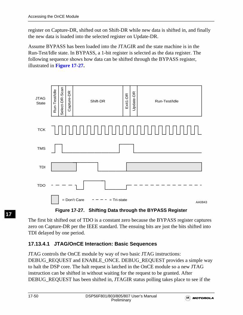
17-50 DSP56F801/803/805/807 User’s Manual�Preliminary
Accessing the OnCE Module
N17
register on Capture-DR, shifted out on Shift-DR while new data is shifted in, and finally the new data is loaded into the selected register on Update-DR.
Assume BYPASS has been loaded into the JTAGIR and the state machine is in the Run-Test/Idle state. In BYPASS, a 1-bit register is selected as the data register. The following sequence shows how data can be shifted through the BYPASS register, illustrated in Figure 17-27.
The first bit shifted out of TDO is a constant zero because the BYPASS register captures zero on Capture-DR per the IEEE standard. The ensuing bits are just the bits shifted into TDI delayed by one period.
17.13.4.1 JTAG/OnCE Interaction: Basic Sequences
JTAG controls the OnCE module by way of two basic JTAG instructions: DEBUG_REQUEST and ENABLE_ONCE. DEBUG_REQUEST provides a simple way to halt the DSP core. The halt request is latched in the OnCE module so a new JTAG instruction can be shifted in without waiting for the request to be granted. After DEBUG_REQUEST has been shifted in, JTAGIR status polling takes place to see if the
Figure 17-27. Shifting Data through the BYPASS Register
JTAGState
TCK
TMS
Sele
ct-D
R-S
can
Update
-DR
Exi
t1-D
R
Captu
re-D
R
Shift-DR
Run-T
est
/Idle
TDI
= Don’t Care
TDO
Run-Test/Idle
= Tri-stateAA0843
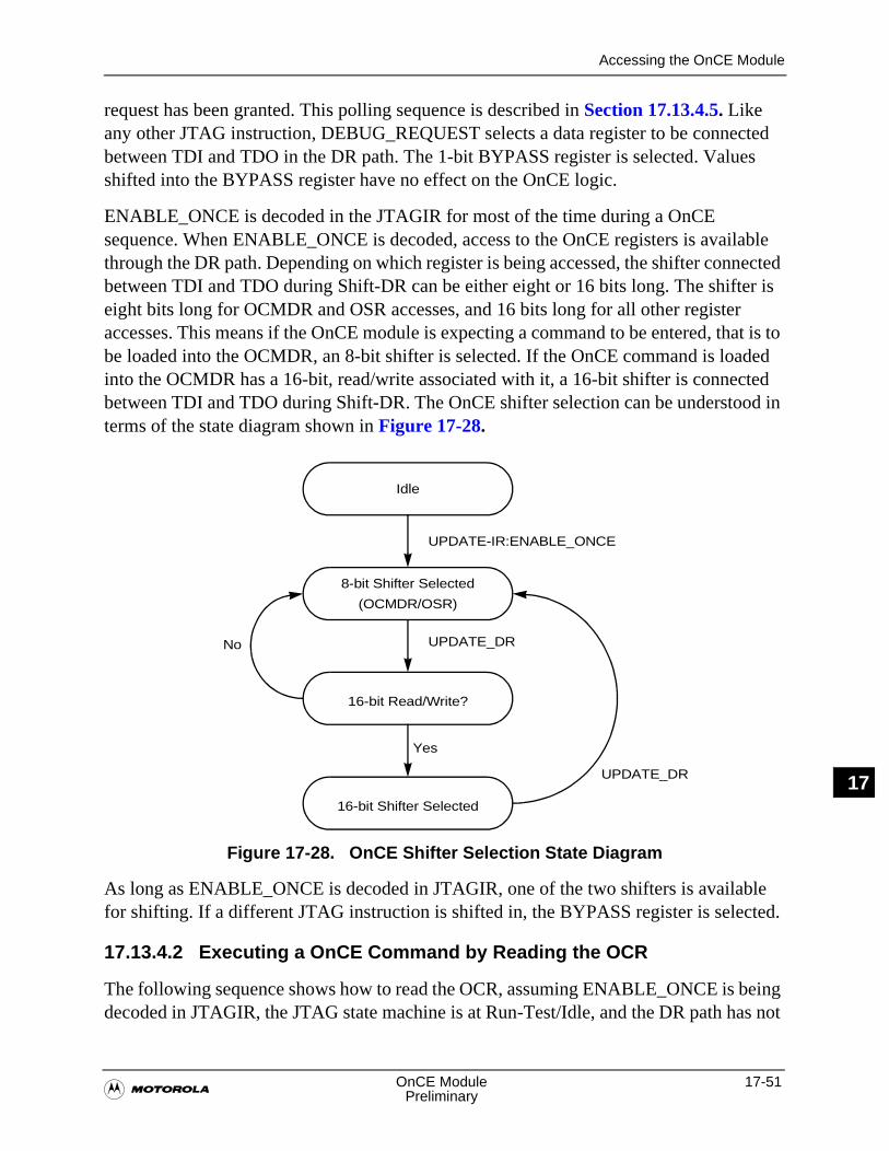
Accessing the OnCE Module
�OnCE Module 17-51
Preliminary
N17
request has been granted. This polling sequence is described in Section 17.13.4.5. Like any other JTAG instruction, DEBUG_REQUEST selects a data register to be connected between TDI and TDO in the DR path. The 1-bit BYPASS register is selected. Values shifted into the BYPASS register have no effect on the OnCE logic.
ENABLE_ONCE is decoded in the JTAGIR for most of the time during a OnCE sequence. When ENABLE_ONCE is decoded, access to the OnCE registers is available through the DR path. Depending on which register is being accessed, the shifter connected between TDI and TDO during Shift-DR can be either eight or 16 bits long. The shifter is eight bits long for OCMDR and OSR accesses, and 16 bits long for all other register accesses. This means if the OnCE module is expecting a command to be entered, that is to be loaded into the OCMDR, an 8-bit shifter is selected. If the OnCE command is loaded into the OCMDR has a 16-bit, read/write associated with it, a 16-bit shifter is connected between TDI and TDO during Shift-DR. The OnCE shifter selection can be understood in terms of the state diagram shown in Figure 17-28.
As long as ENABLE_ONCE is decoded in JTAGIR, one of the two shifters is available for shifting. If a different JTAG instruction is shifted in, the BYPASS register is selected.
17.13.4.2 Executing a OnCE Command by Reading the OCR
The following sequence shows how to read the OCR, assuming ENABLE_ONCE is being decoded in JTAGIR, the JTAG state machine is at Run-Test/Idle, and the DR path has not
Figure 17-28. OnCE Shifter Selection State Diagram
Idle
8-bit Shifter Selected
16-bit Read/Write?
16-bit Shifter Selected
UPDATE_DR
UPDATE_DR
Yes
No
UPDATE-IR:ENABLE_ONCE
(OCMDR/OSR)
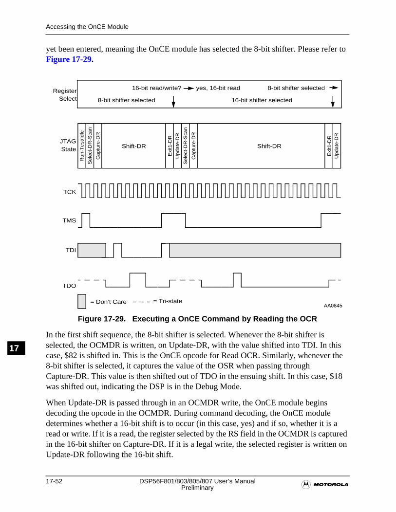
17-52 DSP56F801/803/805/807 User’s Manual�Preliminary
Accessing the OnCE Module
N17
yet been entered, meaning the OnCE module has selected the 8-bit shifter. Please refer to Figure 17-29.
In the first shift sequence, the 8-bit shifter is selected. Whenever the 8-bit shifter is selected, the OCMDR is written, on Update-DR, with the value shifted into TDI. In this case, $82 is shifted in. This is the OnCE opcode for Read OCR. Similarly, whenever the 8-bit shifter is selected, it captures the value of the OSR when passing through Capture-DR. This value is then shifted out of TDO in the ensuing shift. In this case, $18 was shifted out, indicating the DSP is in the Debug Mode.
When Update-DR is passed through in an OCMDR write, the OnCE module begins decoding the opcode in the OCMDR. During command decoding, the OnCE module determines whether a 16-bit shift is to occur (in this case, yes) and if so, whether it is a read or write. If it is a read, the register selected by the RS field in the OCMDR is captured in the 16-bit shifter on Capture-DR. If it is a legal write, the selected register is written on Update-DR following the 16-bit shift.
Figure 17-29. Executing a OnCE Command by Reading the OCR
JTAGState
TCK
TMS
Sel
ect-
DR
-Sca
n
Upd
ate-
DR
Exi
t1-D
R
Cap
ture
-DR
Shift-DR
Run
-Tes
t/Idl
e
TDI
= Don’t Care
TDO
Sel
ect-
DR
-Sca
n
Cap
ture
-DR
Exi
t1-D
RU
pdat
e-D
R
Shift-DR
8-bit shifter selected16-bit read/write? yes, 16-bit read
16-bit shifter selected8-bit shifter selected
RegisterSelect
= Tri-stateAA0845
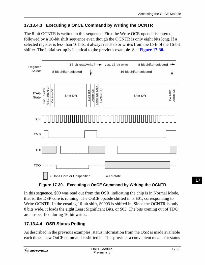
Accessing the OnCE Module
�OnCE Module 17-53
Preliminary
N17
17.13.4.3 Executing a OnCE Command by Writing the OCNTR
The 8-bit OCNTR is written in this sequence. First the Write OCR opcode is entered, followed by a 16-bit shift sequence even though the OCNTR is only eight bits long. If a selected register is less than 16 bits, it always reads to or writes from the LSB of the 16-bit shifter. The initial set-up is identical to the previous example. See Figure 17-30.
In this sequence, $00 was read out from the OSR, indicating the chip is in Normal Mode, that is: the DSP core is running. The OnCE opcode shifted in is $01, corresponding to Write OCNTR. In the ensuing 16-bit shift, $0003 is shifted in. Since the OCNTR is only 8 bits wide, it loads the eight Least Significant Bits, or $03. The bits coming out of TDO are unspecified during 16-bit writes.
17.13.4.4 OSR Status Polling
As described in the previous examples, status information from the OSR is made available each time a new OnCE command is shifted in. This provides a convenient means for status
Figure 17-30. Executing a OnCE Command by Writing the OCNTR
JTAGState
TCK
TMS
Sel
ect-
DR
-Sca
n
Upd
ate-
DR
Exi
t1-D
R
Cap
ture
-DR
Shift-DR
Run
-Tes
t/Idl
e
TDI
= Don’t Care or Unspecified
TDO
Sel
ect-
DR
-Sca
n
Cap
ture
-DR
Exi
t1-D
RU
pdat
e-D
R
Shift-DR
8-bit shifter selected16-bit read/write? yes, 16-bit write
16-bit shifter selected8-bit shifter selected
RegisterSelect
= Tri-state

17-54 DSP56F801/803/805/807 User’s Manual�Preliminary
Accessing the OnCE Module
N17
polling. The following sequence shows the OSR status polling. Assume a breakpoint has been set up to halt the core See Figure 17-31.
On the first 8-bit sequence, $00 is shifted into the OCMDR, corresponding to no-register selected. Next, $00 is read out from the OSR. This read out indicates the DSP core is still in Normal Mode. The OnCE module decodes the $00 opcode and again selects the 8-bit shifter since no 16-bit access is associated with this opcode. On the second 8-bit sequence, $1A is read from the OSR. This read indicates the chip is in the Debug Mode and a hardware breakpoint has occurred.
17.13.4.5 JTAGIR Status Polling
OSR status polling has some disadvantages. First, the OSR is not accessible when the DSP is executing a STOP instruction. OSR access, and all other OnCE register accesses, can continue only after the Stop state has been exited, either by an interrupt or a by DEBUG_REQUEST. Secondly, 8-bit shifts are required. Polling the JTAGIR provides a more efficient and more reliable means of gathering status information. The following
Figure 17-31. OSR Status Polling
JTAGState
TCK
TMS
Sel
ect-
DR
-Sca
n
Upd
ate-
DR
Exi
t1-D
R
Cap
ture
-DR
Shift-DR
Run
-Tes
t/Idl
e
TDI
= don’t care
TDO
Sel
ect-
DR
-Sca
n
Cap
ture
-DR
Exi
t1-D
R
Upd
ate-
DR
Shift-DR
16-bit read/write? no
8-bit shifter selected
RegisterSelect
= Tri-state
8-bit shifter selected
AA0847
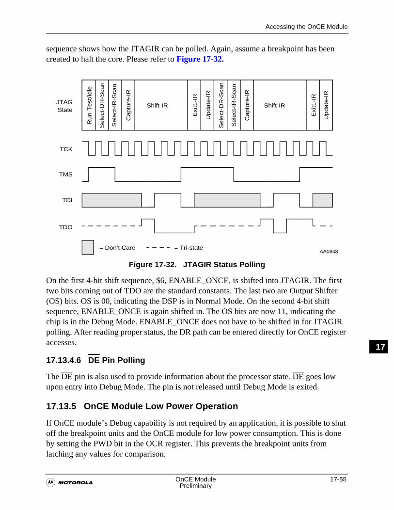
Accessing the OnCE Module
�OnCE Module 17-55
Preliminary
N17
sequence shows how the JTAGIR can be polled. Again, assume a breakpoint has been created to halt the core. Please refer to Figure 17-32.
On the first 4-bit shift sequence, $6, ENABLE_ONCE, is shifted into JTAGIR. The first two bits coming out of TDO are the standard constants. The last two are Output Shifter (OS) bits. OS is 00, indicating the DSP is in Normal Mode. On the second 4-bit shift sequence, ENABLE_ONCE is again shifted in. The OS bits are now 11, indicating the chip is in the Debug Mode. ENABLE_ONCE does not have to be shifted in for JTAGIR polling. After reading proper status, the DR path can be entered directly for OnCE register accesses.
17.13.4.6 DE Pin Polling
The DE pin is also used to provide information about the processor state. DE goes low upon entry into Debug Mode. The pin is not released until Debug Mode is exited.
17.13.5 OnCE Module Low Power Operation
If OnCE module’s Debug capability is not required by an application, it is possible to shut off the breakpoint units and the OnCE module for low power consumption. This is done by setting the PWD bit in the OCR register. This prevents the breakpoint units from latching any values for comparison.
Figure 17-32. JTAGIR Status Polling
JTAGState
TCK
TMS
Sele
ct-D
R-S
can
Update
-IR
Exi
t1-I
R
Run-T
est
/Idle
Sele
ct-I
R-S
can
Captu
re-I
R
Shift-IR
TDI
= Don’t Care
TDO
= Tri-state
Sele
ct-D
R-S
can
Sele
ct-I
R-S
can
Captu
re-I
R
Shift-IR
Exi
t1-I
R
Update
-IR
AA0848
17-56 DSP56F801/803/805/807 User’s Manual�Preliminary
Accessing the OnCE Module
N17
17.13.6 Resetting the Chip Without Resetting the OnCE Unit
DSP can be reset without resetting the OnCE module. This reset allows creating breakpoints on an application’s final target hardware with a potential power-on reset circuit. The OnCE module reset is disabled using the following technique: If an ENABLE_ONCE instruction is in the JTAGIR when a hardware or COP timer reset occurs, then the OnCE module unit is not reset. All OnCE module registers retain their current values while all valid breakpoints remain enabled. If any other instruction is in the JTAGIR when a chip reset occurs, the OnCE module is reset. The preceding capabilities permits the following sequence, useful for setting breakpoints on final target hardware:
1. Reset the DSP chip using the RESET pin.
2. Come out of reset and begin to execute the application code, perhaps out of Program ROM if this is where the user’s application code is located.
3. Halt the DSP chip and enter the Debug Mode.
4. Program the desired breakpoint(s) and leave the ENABLE_ONCE instruction in the JTAGIR.
5. Reset the DSP chip using the RESET pin again, but this time the OnCE module is not reset and the breakpoints remain valid and enabled.
6. Come out of reset and begin to execute the application code, perhaps out of Program ROM if this is where the user’s application code is located.
7. The DSP chip then correctly triggers in the application code when the desired breakpoint condition is detected.
8. The JTAG port can be polled to detect the occurrence of this breakpoint.
Another technique for loading breakpoints is achieved as follows:
1. Reset the DSP chip by asserting both the RESET pin and the TRST pin.
2. Release the TRST pin.
3. Shift in a ENABLE_ONCE instruction into the JTAGIR.
4. Set up the desired breakpoints.
5. Release the RESET pin.
6. Come out of reset and begin to execute the application code.
7. The DSP chip then correctly triggers in the application code when the desired breakpoint condition is detected.
8. The JTAG port can be polled to detect the occurrence of this breakpoint.
Accessing the OnCE Module
�OnCE Module 17-57
Preliminary
N17
Another useful sequence is to enter the Debug Mode directly from reset. This sequence is approached as follows:
1. Reset the DSP chip by asserting both the RESET pin and the TRST pin.
2. Release the TRST pin.
3. Shift in a DEBUG_REQUEST instruction into the JTAGIR.
4. Release the RESET pin.
5. Come out of reset and directly enter the Debug Mode.
The OnCE module reset can still be forced on DSP chip reset even if there is an ENABLE_ONCE instruction in the JTAGIR. This is accomplished by asserting the TRST pin in addition to the RESET pin, guaranteeing reset of the OnCE module.
17-58 DSP56F801/803/805/807 User’s Manual�Preliminary
Accessing the OnCE Module
N17

�JTAG Port Introduction 18-1
Preliminary
N18
Chapter 18JTAG Port Introduction

18-2 DSP56F801/803/805/807 User’s Manual�Preliminary
ON18
Introduction
�JTAG Port Introduction 18-3
Preliminary
N18
18.1 Introduction
More about debugging and high-density circuit board testing specific to Joint Test Action Group.
Like the previous chapter, this chapter is dedicated to testing and debugging retention, but specifically through the Joint Test Action Group, (JTAG) and the OnCE module.
DSP56F801/803/805/807 provides board and chip-level testing capability through two on-chip modules, both accessed through the JTAG port/OnCE module interface:
• On-chip Emulation (OnCE) module
• Test Access Port (TAP) and 16-state controller, also known as the Joint Test Action Group (JTAG) port
Presence of the JTAG port/OnCE module interface permits insertion of the DSP chip into a target system while retaining debug control. This capability is especially important for devices without an external bus, because it eliminates the need for a costly cable to bring out the footprint of the chip required by a traditional emulator system.
The OnCE module is a Motorola-designed module used in Digital Signal Processor (DSP) chips to debug application software employed with the chip. The port is a separate on-chip block allowing non-intrusive DSP interaction with accessibility through the pins of the JTAG interface. The OnCE module makes it possible to examine registers, memory, or on-chip peripherals’ contents in a special debug environment. This avoids sacrificing any user-accessible on-chip resources to perform debugging. See Chapter 17, OnCE Module for details on the OnCE module implementation of the DSP56F801,803, 805 and 807 series.
The JTAG port is a dedicated user-accessible TAP compatible with the IEEE 1149.1a-1993 Standard Test Access Port and Boundary Scan Architecture. Problems associated with testing high-density circuit boards have led to the development of this proposed standard under the sponsorship of the Test Technology Committee of IEEE and the JTAG. DSP56F 801 through 807 supports circuit board test strategies based on this standard.
Five dedicated pins interface to the TAP containing a 16-state controller. The TAP uses a boundary scan technique to test the interconnections between integrated circuits after they are assembled onto a Printed Circuit Board (PCB). Boundary scans allow a tester to observe and control signal levels at each component pin through a shift register placed next to each pin. This is important for testing continuity and determining if pins are stuck at a one or zero level.
18-4 DSP56F801/803/805/807 User’s Manual�Preliminary
Features
ON18
18.2 Features
Features of the TAP port include the following:
• Perform boundary scan operations to test circuit board electrical continuity
• Bypass the DSP for a given circuit board test by replacing the Boundary Scan Register (BSR) with a single-bit register
• Sample the DSP system pins during operation and transparently shift out the result in the CSR; pre-load values to output pins prior to invoking the EXTEST instruction
• Disable the output drive to pins during circuit board testing
• Provide a means of accessing the OnCE module controller and circuits to control a target system
• Query identification information, manufacturer, pat number, and version from a DSP chip
• Force test data onto the outputs of a DSP IC while replacing its BSR in the serial data path with a single bit register
• Enable a weak pull-up current device on all input signals of a DSP IC, helping to assure deterministic test results in the presence of continuity fault during interconnect testing
This chapter includes aspects of the JTAG implementation specific to the DSP56F801 through 807. Chapter data is intended to be utilized with IEEE 1149.1a. The discussion includes those items required by the standard to be defined and, in certain cases, provide additional information specific to the DSP56F801/803/805/807. For internal details and applications of the standard, refer to IEEE 1149.1a.
18.3 Pin Descriptions
As described in IEEE 1149.1a, the JTAG port requires a minimum of four pins to support TDI, TDO, TCK, and TMS signals. The DSP56F801/803/805/807 also uses the optional TRST input signal and DE output signal used by the OnCE module interface. The pin functions are described in Table 18-1.
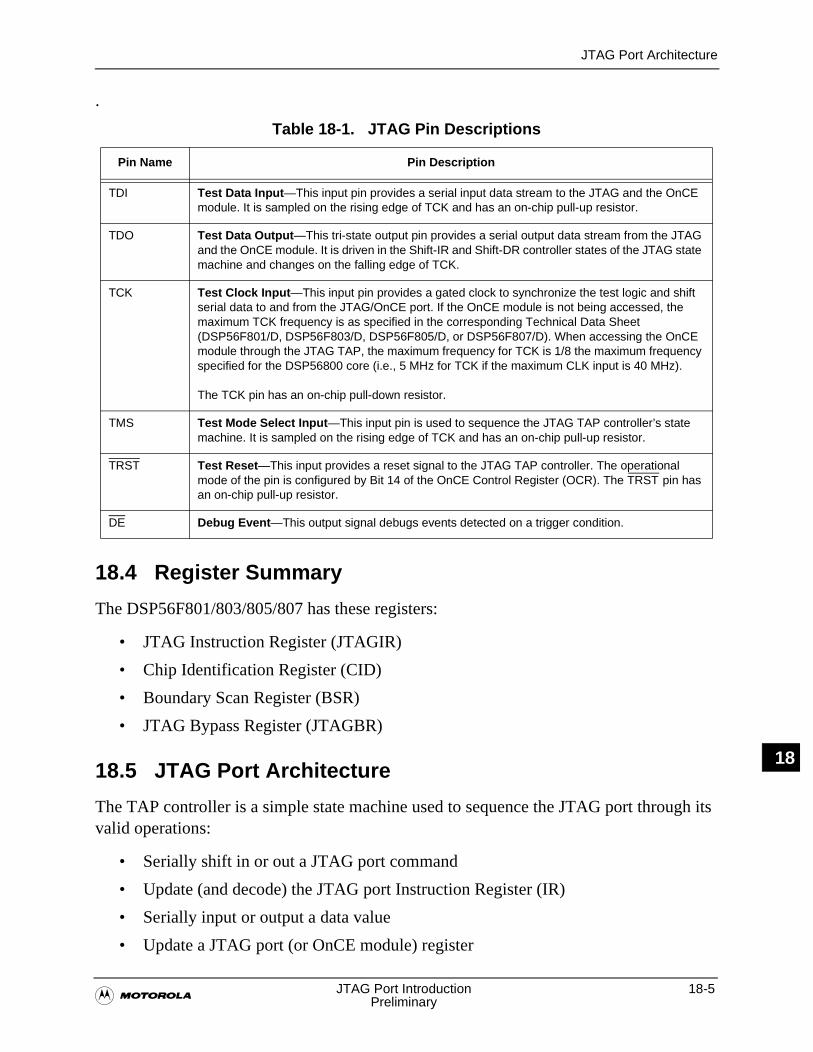
JTAG Port Architecture
�JTAG Port Introduction 18-5
Preliminary
N18
.
18.4 Register Summary
The DSP56F801/803/805/807 has these registers:
• JTAG Instruction Register (JTAGIR)
• Chip Identification Register (CID)
• Boundary Scan Register (BSR)
• JTAG Bypass Register (JTAGBR)
18.5 JTAG Port Architecture
The TAP controller is a simple state machine used to sequence the JTAG port through its valid operations:
• Serially shift in or out a JTAG port command
• Update (and decode) the JTAG port Instruction Register (IR)
• Serially input or output a data value
• Update a JTAG port (or OnCE module) register
Table 18-1. JTAG Pin Descriptions
Pin Name Pin Description
TDI Test Data Input—This input pin provides a serial input data stream to the JTAG and the OnCE module. It is sampled on the rising edge of TCK and has an on-chip pull-up resistor.
TDO Test Data Output—This tri-state output pin provides a serial output data stream from the JTAG and the OnCE module. It is driven in the Shift-IR and Shift-DR controller states of the JTAG state machine and changes on the falling edge of TCK.
TCK Test Clock Input—This input pin provides a gated clock to synchronize the test logic and shift serial data to and from the JTAG/OnCE port. If the OnCE module is not being accessed, the maximum TCK frequency is as specified in the corresponding Technical Data Sheet (DSP56F801/D, DSP56F803/D, DSP56F805/D, or DSP56F807/D). When accessing the OnCE module through the JTAG TAP, the maximum frequency for TCK is 1/8 the maximum frequency specified for the DSP56800 core (i.e., 5 MHz for TCK if the maximum CLK input is 40 MHz).
The TCK pin has an on-chip pull-down resistor.
TMS Test Mode Select Input—This input pin is used to sequence the JTAG TAP controller’s state machine. It is sampled on the rising edge of TCK and has an on-chip pull-up resistor.
TRST Test Reset—This input provides a reset signal to the JTAG TAP controller. The operational mode of the pin is configured by Bit 14 of the OnCE Control Register (OCR). The TRST pin has an on-chip pull-up resistor.
DE Debug Event—This output signal debugs events detected on a trigger condition.
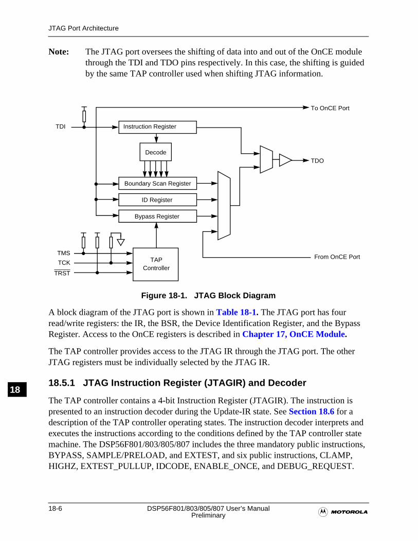
18-6 DSP56F801/803/805/807 User’s Manual�Preliminary
JTAG Port Architecture
ON18
Note: The JTAG port oversees the shifting of data into and out of the OnCE module through the TDI and TDO pins respectively. In this case, the shifting is guided by the same TAP controller used when shifting JTAG information.
A block diagram of the JTAG port is shown in Table 18-1. The JTAG port has four read/write registers: the IR, the BSR, the Device Identification Register, and the Bypass Register. Access to the OnCE registers is described in Chapter 17, OnCE Module.
The TAP controller provides access to the JTAG IR through the JTAG port. The other JTAG registers must be individually selected by the JTAG IR.
18.5.1 JTAG Instruction Register (JTAGIR) and Decoder
The TAP controller contains a 4-bit Instruction Register (JTAGIR). The instruction is presented to an instruction decoder during the Update-IR state. See Section 18.6 for a description of the TAP controller operating states. The instruction decoder interprets and executes the instructions according to the conditions defined by the TAP controller state machine. The DSP56F801/803/805/807 includes the three mandatory public instructions, BYPASS, SAMPLE/PRELOAD, and EXTEST, and six public instructions, CLAMP, HIGHZ, EXTEST_PULLUP, IDCODE, ENABLE_ONCE, and DEBUG_REQUEST.
Figure 18-1. JTAG Block Diagram
TAPController
Boundary Scan Register
TDO
TMS
TCK
ID Register
Bypass Register
Decode
To OnCE Port
From OnCE Port
TRST
Instruction RegisterTDI
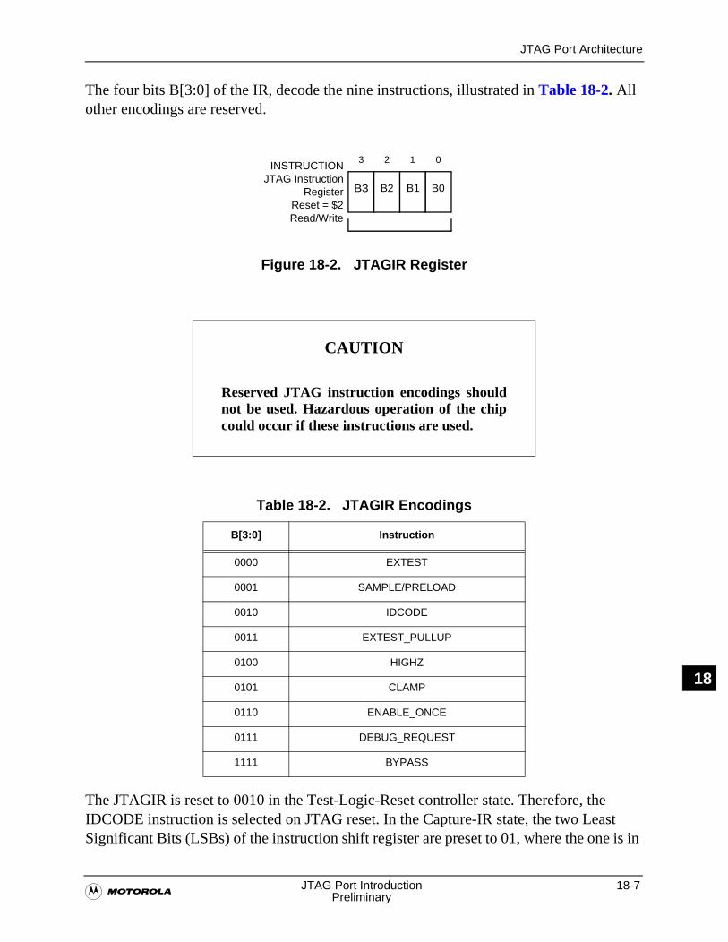
JTAG Port Architecture
�JTAG Port Introduction 18-7
Preliminary
N18
The four bits B[3:0] of the IR, decode the nine instructions, illustrated in Table 18-2. All other encodings are reserved.
Figure 18-2. JTAGIR Register
The JTAGIR is reset to 0010 in the Test-Logic-Reset controller state. Therefore, the IDCODE instruction is selected on JTAG reset. In the Capture-IR state, the two Least Significant Bits (LSBs) of the instruction shift register are preset to 01, where the one is in
CAUTION
Reserved JTAG instruction encodings shouldnot be used. Hazardous operation of the chipcould occur if these instructions are used.
Table 18-2. JTAGIR Encodings
B[3:0] Instruction
0000 EXTEST
0001 SAMPLE/PRELOAD
0010 IDCODE
0011 EXTEST_PULLUP
0100 HIGHZ
0101 CLAMP
0110 ENABLE_ONCE
0111 DEBUG_REQUEST
1111 BYPASS
INSTRUCTIONJTAG Instruction
RegisterReset = $2Read/Write
B3
3 2 1 0
B1 B0B2
18-8 DSP56F801/803/805/807 User’s Manual�Preliminary
JTAG Port Architecture
ON18
the LSB location as required by the standard. The two Most Significant Bits (MSBs) may either capture status or be set to zero. New instructions are moved into the instruction shift register stage in Shift-IR state.
18.5.1.1 EXTEST (B[3:0] = 0000)
The external test (EXTEST) instruction enables the BSR between TDI and TDO, including cells for all digital device signals and associated control signals. The EXTAL pin, and any codec pins associated with analog signals, are not included in the BSR path.
In EXTEST, the BSR is capable of scanning user-defined values onto output pins, capturing values presented to input signals, and controlling the direction and value of bidirectional pins. EXTEST instruction asserts internal system reset for the DSP system logic during its run in order to force a predictable internal state while performing external boundary scan operations.
18.5.1.2 SAMPLE/PRELOAD (B[3:0] = 0001)
The SAMPLE/PRELOAD instruction enables the BSR between TDI and TDO. When this instruction is selected, the test logic operation has no effect on the operation of the on-chip system logic. Nor does it have an effect on the flow of a signal between the system pin and the on-chip system logic, as specified by IEEE 1149.1-1993a. This instruction provides two separate functions. First, it provides a means to obtain a snapshot of system data and control signals (SAMPLE). The snapshot occurs on the rising edge of TCK in the Capture-DR controller state. The data can be observed by shifting it transparently through the BSR.
In a normal system configuration, many signals require external pull-ups assuring proper system operation. Consequently, the same is true for the SAMPLE/PRELOAD functionality. Data latched into the BSR during the Capture-DR controller state may not match the drive state of the package signal if the system-requiring pull-ups are not present within the test environment.
The second function of the SAMPLE/PRELOAD instruction is to initialize the BSR output cells (PRELOAD) prior to selection of the CLAMP, EXTEST, or EXTEST_PULLUP instruction. This initialization ensures known data appears on the outputs when executing EXTEST. The data held in the shift register stage is transferred to the output latch on the falling edge of TCK in the Update-DR controller state. Data is not presented to the pins until the CLAMP, EXTEST, or EXTEST_PULLUP instruction is executed.
Note: Since there is no internal synchronization between the JTAG clock (TCK) and the system clock (CLK), some form of external synchronization to achieve
JTAG Port Architecture
�JTAG Port Introduction 18-9
Preliminary
N18
meaningful results when sampling system values using the SAMPLE/PRELOAD instruction must be provided.
18.5.1.3 IDCODE (B[3:0] = 0010)
The IDCODE instruction enables the IDREGISTER between TDI and TDO. It is provided as a public instruction to allow the manufacturer, part number, and version of a component to be determined through the TAP.
When the IDCODE instruction is decoded, it selects the IDREGISTER, a 32-bit test data register. IDREGISTER loads a constant logic one into its LSB. Since the Bypass Register loads a logic zero at the start of a scan cycle, examination of the first bit of data shifted out of a component during a test data scan sequence immediately following exit from the Test-Logic-Reset controller state shows whether an IDREGISTER is included in the design.
When the IDCODE instruction is selected, the operation of the test logic has no effect on the operation of the on-chip system logic, as required in IEEE 1149.1a-1993.
18.5.1.4 EXTEST_PULLUP (B[3:0] = 0011)
The EXTEST_PULLUP instruction is provided as a public instruction to aid in fault diagnoses during boundary scan testing of a circuit board. This instruction functions similarly to EXTEST, with the only difference being the presence of a weak pull-up device on all input signals. Given an appropriate charging delay, the pull-up current supplies a deterministic logic one result on an open input. When this instruction is used in board-level testing with heavily loaded nodes, it may require a charging delay greater than the two TCK periods needed to transition from the Update-DR state to the Capture-DR state. Two methods of providing an increase delay are available: traverse into the Run-Test/Idle state for extra TCK periods of charging delay, or limit the maximum TCK frequency, slow down the TCK, so two TCK periods are adequate. The EXTEST_PULLUP instruction asserts internal system reset for the DSP system logic for the duration of EXTEST_PULLUP in order to force a predictable internal state while performing external boundary scan operations.
18.5.1.5 HIGHZ (B[3:0] = 0100)
The HIGHZ instruction enables the single-bit Bypass Register between TDI and TDO. It is provided as a public instruction in order to prevent having to drive the output signals back during circuit board testing. When the HIGHZ instruction is invoked, all output drivers are placed in an inactive-drive state. HIGHZ asserts internal system reset for the DSP system logic for the duration of HIGHZ in order to force a predictable internal state while performing external boundary scan operations.
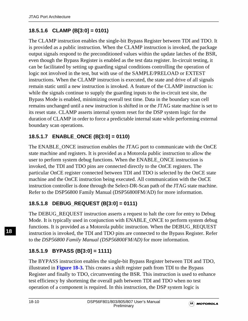
18-10 DSP56F801/803/805/807 User’s Manual�Preliminary
JTAG Port Architecture
ON18
18.5.1.6 CLAMP (B[3:0] = 0101)
The CLAMP instruction enables the single-bit Bypass Register between TDI and TDO. It is provided as a public instruction. When the CLAMP instruction is invoked, the package output signals respond to the preconditioned values within the update latches of the BSR, even though the Bypass Register is enabled as the test data register. In-circuit testing, it can be facilitated by setting up guarding signal conditions controlling the operation of logic not involved in the test, but with use of the SAMPLE/PRELOAD or EXTEST instructions. When the CLAMP instruction is executed, the state and drive of all signals remain static until a new instruction is invoked. A feature of the CLAMP instruction is: while the signals continue to supply the guarding inputs to the in-circuit test site, the Bypass Mode is enabled, minimizing overall test time. Data in the boundary scan cell remains unchanged until a new instruction is shifted in or the JTAG state machine is set to its reset state. CLAMP asserts internal system reset for the DSP system logic for the duration of CLAMP in order to force a predictable internal state while performing external boundary scan operations.
18.5.1.7 ENABLE_ONCE (B[3:0] = 0110)
The ENABLE_ONCE instruction enables the JTAG port to communicate with the OnCE state machine and registers. It is provided as a Motorola public instruction to allow the user to perform system debug functions. When the ENABLE_ONCE instruction is invoked, the TDI and TDO pins are connected directly to the OnCE registers. The particular OnCE register connected between TDI and TDO is selected by the OnCE state machine and the OnCE instruction being executed. All communication with the OnCE instruction controller is done through the Select-DR-Scan path of the JTAG state machine. Refer to the DSP56800 Family Manual (DSP56800FM/AD) for more information.
18.5.1.8 DEBUG_REQUEST (B[3:0] = 0111)
The DEBUG_REQUEST instruction asserts a request to halt the core for entry to Debug Mode. It is typically used in conjunction with ENABLE_ONCE to perform system debug functions. It is provided as a Motorola public instruction. When the DEBUG_REQUEST instruction is invoked, the TDI and TDO pins are connected to the Bypass Register. Refer to the DSP56800 Family Manual (DSP56800FM/AD) for more information.
18.5.1.9 BYPASS (B[3:0] = 1111)
The BYPASS instruction enables the single-bit Bypass Register between TDI and TDO, illustrated in Figure 18-3. This creates a shift register path from TDI to the Bypass Register and finally to TDO, circumventing the BSR. This instruction is used to enhance test efficiency by shortening the overall path between TDI and TDO when no test operation of a component is required. In this instruction, the DSP system logic is
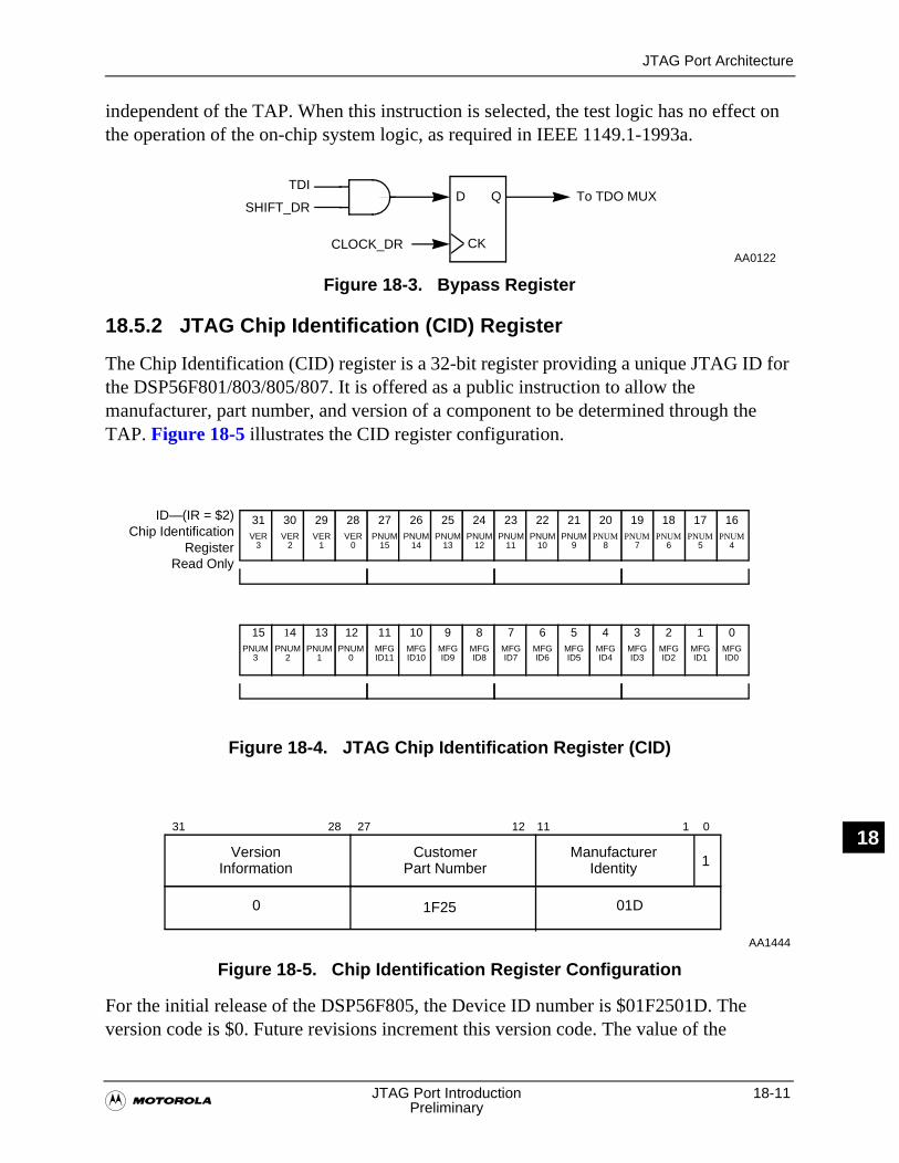
JTAG Port Architecture
�JTAG Port Introduction 18-11
Preliminary
N18
independent of the TAP. When this instruction is selected, the test logic has no effect on the operation of the on-chip system logic, as required in IEEE 1149.1-1993a.
18.5.2 JTAG Chip Identification (CID) Register
The Chip Identification (CID) register is a 32-bit register providing a unique JTAG ID for the DSP56F801/803/805/807. It is offered as a public instruction to allow the manufacturer, part number, and version of a component to be determined through the TAP. Figure 18-5 illustrates the CID register configuration.
Figure 18-4. JTAG Chip Identification Register (CID)
For the initial release of the DSP56F805, the Device ID number is $01F2501D. The version code is $0. Future revisions increment this version code. The value of the
Figure 18-3. Bypass Register
Figure 18-5. Chip Identification Register Configuration
D QSHIFT_DR
CLOCK_DR CK
TDITo TDO MUX
AA0122
ID—(IR = $2)Chip Identification
RegisterRead Only
MFGMFG MFGMFG MFGMFG MFG MFGID7 ID6 ID5 ID4 ID3 ID2 ID1 ID0
7 6 5 4 3 2 1 0MFG MFGMFG MFG
ID11 ID10 ID9 ID8
11 10 9 8PNUM PNUMPNUM PNUM
3 2 1 0
15 14 13 12
PNUMPNUM PNUMPNUM PNUMPNUM PNUM PNUM11 10 9 8 7 6 5 4
23 22 21 20 19 18 17 16PNUM PNUMPNUM PNUM
15 14 13 12
27 26 25 24VER VERVER VER
3 2 1 0
31 30 29 28
011112272831
ManufacturerIdentityPart Number
VersionInformation
Customer1
0 01D
AA1444
1F25
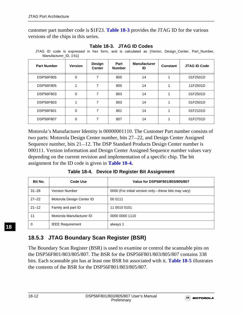
18-12 DSP56F801/803/805/807 User’s Manual�Preliminary
JTAG Port Architecture
ON18
customer part number code is $1F23. Table 18-3 provides the JTAG ID for the various versions of the chips in this series.
Table 18-3. JTAG ID CodesJTAG ID code is expressed in hex form, and is calculated as (Verion, Design_Center, Part_Number,
Manufacturer_ID, 1’b1)
Motorola’s Manufacturer Identity is 00000001110. The Customer Part number consists of two parts: Motorola Design Center number, bits 27—22, and Design Center Assigned Sequence number, bits 21—12. The DSP Standard Products Design Center number is 000111. Version information and Design Center Assigned Sequence number values vary depending on the current revision and implementation of a specific chip. The bit assignment for the ID code is given in Table 18-4.
18.5.3 JTAG Boundary Scan Register (BSR)
The Boundary Scan Register (BSR) is used to examine or control the scannable pins on the DSP56F801/803/805/807. The BSR for the DSP56F801/803/805/807 contains 338 bits. Each scannable pin has at least one BSR bit associated with it. Table 18-5 illustrates the contents of the BSR for the DSP56F801/803/805/807.
Part Number VersionDesign Center
Part Number
Manufacturer ID
Constant JTAG ID Code
DSP56F805 0 7 805 14 1 01F2501D
DSP56F805 1 7 805 14 1 11F2501D
DSP56F803 0 7 803 14 1 01F2501D
DSP56F803 1 7 803 14 1 01F2501D
DSP56F801 0 7 801 14 1 01F2101D
DSP56F807 0 7 807 14 1 01F2701D
Table 18-4. Device ID Register Bit Assignment
Bit No. Code Use Value for DSP56F801/803/805/807
31–28 Version Number 0000 (For initial version only—these bits may vary)
27–22 Motorola Design Center ID 00 0111
21–12 Family and part ID 11 0010 0101
11 Motorola Manufacturer ID 0000 0000 1110
0 IEEE Requirement always 1
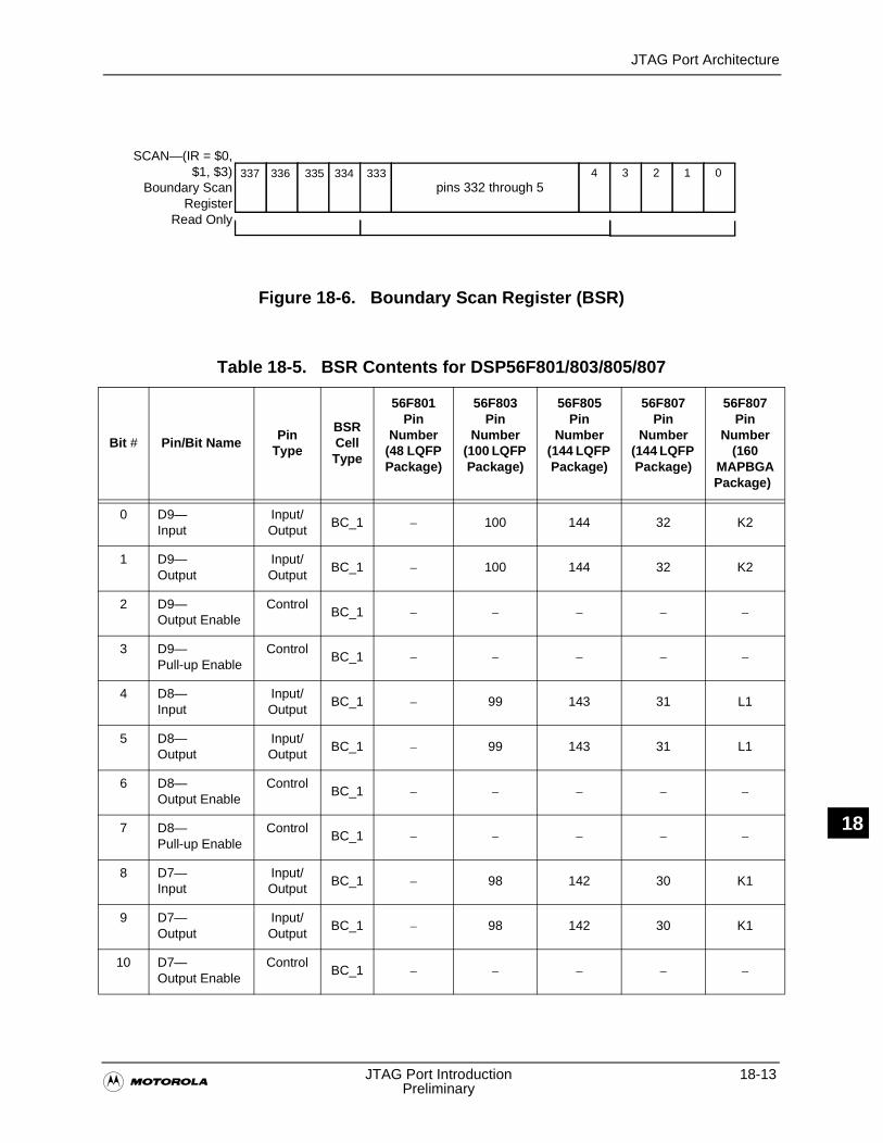
JTAG Port Architecture
�JTAG Port Introduction 18-13
Preliminary
N18
Figure 18-6. Boundary Scan Register (BSR)
Table 18-5. BSR Contents for DSP56F801/803/805/807
Bit # Pin/Bit NamePin
Type
BSR Cell Type
56F801 Pin
Number(48 LQFP Package)
56F803 Pin
Number(100 LQFP Package)
56F805 Pin
Number(144 LQFP Package)
56F807 Pin
Number(144 LQFP Package)
56F807 Pin
Number(160
MAPBGAPackage)
0 D9—Input
Input/Output
BC_1 – 100 144 32 K2
1 D9—Output
Input/Output
BC_1 – 100 144 32 K2
2 D9—Output Enable
ControlBC_1 – – – – –
3 D9—Pull-up Enable
ControlBC_1 – – – – –
4 D8—Input
Input/Output
BC_1 – 99 143 31 L1
5 D8—Output
Input/Output
BC_1 – 99 143 31 L1
6 D8—Output Enable
ControlBC_1 – – – – –
7 D8—Pull-up Enable
ControlBC_1 – – – – –
8 D7—Input
Input/Output
BC_1 – 98 142 30 K1
9 D7—Output
Input/Output
BC_1 – 98 142 30 K1
10 D7—Output Enable
ControlBC_1 – – – – –
SCAN—(IR = $0,$1, $3)
Boundary ScanRegister
Read Only
pins 332 through 5333337 336 335 334 4 3 2 1 0
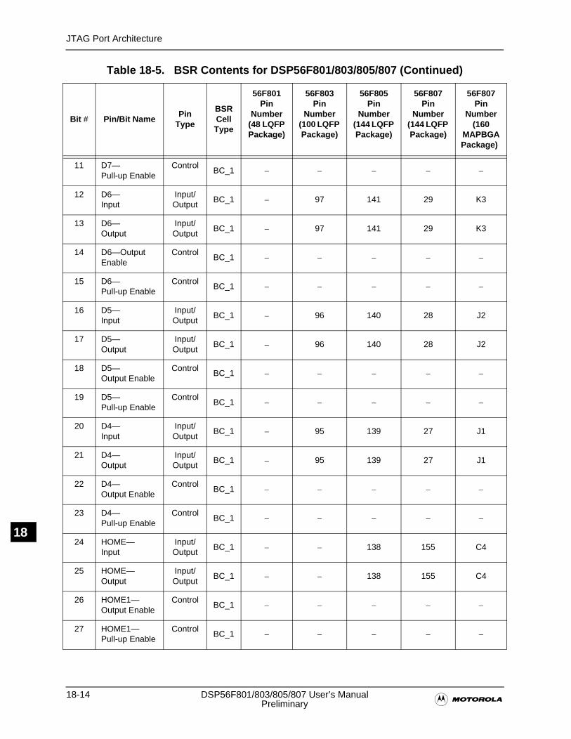
18-14 DSP56F801/803/805/807 User’s Manual�Preliminary
JTAG Port Architecture
ON18
11 D7—Pull-up Enable
ControlBC_1 – – – – –
12 D6—Input
Input/Output
BC_1 – 97 141 29 K3
13 D6—Output
Input/Output
BC_1 – 97 141 29 K3
14 D6—Output Enable
ControlBC_1 – – – – –
15 D6—Pull-up Enable
ControlBC_1 – – – – –
16 D5—Input
Input/Output
BC_1 – 96 140 28 J2
17 D5—Output
Input/Output
BC_1 – 96 140 28 J2
18 D5—Output Enable
ControlBC_1 – – – – –
19 D5—Pull-up Enable
ControlBC_1 – – – – –
20 D4—Input
Input/Output
BC_1 – 95 139 27 J1
21 D4—Output
Input/Output
BC_1 – 95 139 27 J1
22 D4—Output Enable
ControlBC_1 – – – – –
23 D4—Pull-up Enable
ControlBC_1 – – – – –
24 HOME—Input
Input/Output
BC_1 – – 138 155 C4
25 HOME—Output
Input/Output
BC_1 – – 138 155 C4
26 HOME1—Output Enable
ControlBC_1 – – – – –
27 HOME1—Pull-up Enable
ControlBC_1 – – – – –
Table 18-5. BSR Contents for DSP56F801/803/805/807 (Continued)
Bit # Pin/Bit NamePin
Type
BSR Cell Type
56F801 Pin
Number(48 LQFP Package)
56F803 Pin
Number(100 LQFP Package)
56F805 Pin
Number(144 LQFP Package)
56F807 Pin
Number(144 LQFP Package)
56F807 Pin
Number(160
MAPBGAPackage)

JTAG Port Architecture
�JTAG Port Introduction 18-15
Preliminary
N18
28 D3—Input
Input/Output
BC_1 – 94 137 26 J3
29 D3—Output
Input/Output
BC_1 – 94 137 26 J3
30 D3—Output Enable
ControlBC_1 – – – – –
31 D3—Pull-up Enable
ControlBC_1 – – – – –
32 PHASEA1—Input
Input/Output
BC_1 – – 136 151 E4
33 PHASEA1—Output
Input/Output
BC_1 – – 136 151 E4
34 PHASEA1—Output Enable
ControlBC_1 – – – – –
35 PHASEA1—Pull-up Enable
ControlBC_1 – – – – –
36 PHASEB1—Input
Input/Output
BC_1 – – 134 152 B5
37 PHASEB1—Output
Input/Output
BC_1 – – 134 152 B5
38 PHASEB1—Output Enable
ControlBC_1 – – – – –
39 PHASEB1—Pull-up Enable
ControlBC_1 – – – – –
40 INDEX1—Input
Input/Output
BC_1 – – 132 149 D4
41 INDX1—Output
Input/Output
BC_1 – – 132 149 D4
42 INDX1—Output Enable
ControlBC_1 – – – – –
43 INDX1—Pull-up Enable
ControlBC_1 – – – – –
44 D2—Input
Input/Output
BC_1 – 91 131 25 H2
Table 18-5. BSR Contents for DSP56F801/803/805/807 (Continued)
Bit # Pin/Bit NamePin
Type
BSR Cell Type
56F801 Pin
Number(48 LQFP Package)
56F803 Pin
Number(100 LQFP Package)
56F805 Pin
Number(144 LQFP Package)
56F807 Pin
Number(144 LQFP Package)
56F807 Pin
Number(160
MAPBGAPackage)

18-16 DSP56F801/803/805/807 User’s Manual�Preliminary
JTAG Port Architecture
ON18
45 D2—Output
Input/Output
BC_1 – 91 131 25 H2
46 D2—Output Enable
ControlBC_1 – – – – –
47 D2—Pull-up Enable
ControlBC_1 – – – – –
48 D1—Input
Input/Output
BC_1 – 90 130 24 H1
49 D1—Output
Input/Output
BC_1 – 90 130 24 H1
50 D1—Output Enable
ControlBC_1 – – – – –
51 D1—Pull-up Enable
ControlBC_1 – – – – –
52 D0—Input
Input/Output
BC_1 – 89 128 23 H3
53 D0—Output
Input/Output
BC_1 – 89 128 23 H3
54 D0—Output Enable
ControlBC_1 – – – – –
55 D0—Pull-up Enable
ControlBC_1 – – – – –
56 MPIOD5—Input
Input/Output
BC_1 – – 127 54 K6
57 MPIOD5—Output
Input/Output
BC_1 – – 127 54 K6
58 MPIOD5—Output Enable
ControlBC_1 – – – – –
59 MPIOD5—Pull-up Enable
ControlBC_1 – – – – –
60 SCLK—Input
Input/Output
BC_1 7 87 125 144 E5
61 SCLK—Output
Input/Output
BC_1 7 87 125 144 E5
Table 18-5. BSR Contents for DSP56F801/803/805/807 (Continued)
Bit # Pin/Bit NamePin
Type
BSR Cell Type
56F801 Pin
Number(48 LQFP Package)
56F803 Pin
Number(100 LQFP Package)
56F805 Pin
Number(144 LQFP Package)
56F807 Pin
Number(144 LQFP Package)
56F807 Pin
Number(160
MAPBGAPackage)

JTAG Port Architecture
�JTAG Port Introduction 18-17
Preliminary
N18
62 SCLK—Output Enable
ControlBC_1 – – – – –
63 SCLK—Pull-up Enable
ControlBC_1 – – – – –
64 MOSI—Input
Input/Output
BC_1 6 86 124 146 A6
65 MOSI—Output
Input/Output
BC_1 6 86 124 146 A6
66 MOSI—Output Enable
ControlBC_1 – – – – –
67 MOSI—Pull-up Enable
ControlBC_1 – – – – –
68 MPIOD4—Input
Input/Output
BC_1 – – 123 53 L6
69 MPIOD4—Output
Input/Output
BC_1 – – 123 53 L6
70 MPIOD4—Output Enable
ControlBC_1 – – – – –
71 MPIOD4—Pull-up Enable
ControlBC_1 – – – – –
72 MISO—Input
Input/Output
BC_1 5 85 122 145 B7
73 MISO—Output
Input/Output
BC_1 5 85 122 145 B7
74 MISO—Output Enable
ControlBC_1 – – – – –
75 MISO—Pull-up Enable
ControlBC_1 – – – – –
76 MPIOD3—Input
Input/Output
BC_1 – – 121 52 M6
77 MPIOD3—Output
Input/Output
BC_1 – – 121 52 M6
78 MPIOD3—Output Enable
ControlBC_1 – – – – –
Table 18-5. BSR Contents for DSP56F801/803/805/807 (Continued)
Bit # Pin/Bit NamePin
Type
BSR Cell Type
56F801 Pin
Number(48 LQFP Package)
56F803 Pin
Number(100 LQFP Package)
56F805 Pin
Number(144 LQFP Package)
56F807 Pin
Number(144 LQFP Package)
56F807 Pin
Number(160
MAPBGAPackage)

18-18 DSP56F801/803/805/807 User’s Manual�Preliminary
JTAG Port Architecture
ON18
79 MPIDO3—Pull-up Enable
ControlBC_1 – – – – –
80 SS—Input
Input/Output
BC_1 4 84 120 143 A7
81 SS—Output
Input/Output
BC_1 4 84 120 143 A7
82 SS—Output Enable
ControlBC_1 – – – – –
83 SS—Pull-up Enable
ControlBC_1 – – – – –
84 RSTO—Output
OutputBC_1 – – 119 97 H12
85 RSTO—Output Enable
ControlBC_1 – – – – –
86 TD3—Input
Input/Output
BC_1 – – 118 129 B10
87 TD3—Output
Input/Output
BC_1 – – 118 129 B10
88 TD3—Output Enable
ControlBC_1 – – – – –
89 TD3—Pull-up Enable
ControlBC_1 – – – – –
90 TD2—Input
Input/Output
BC_1 3 83 116 128 D10
91 TD2—Output
Input/Output
BC_1 3 83 116 128 D10
92 TD2—Output Enable
ControlBC_1 – – – – –
93 TD2—Pull-up Enable
ControlBC_1 – – – – –
94 TD1—Input
Input/Output
BC_1 2 82 114 127 A11
95 TD1—Output
Input/Output
BC_1 2 82 114 127 A11
Table 18-5. BSR Contents for DSP56F801/803/805/807 (Continued)
Bit # Pin/Bit NamePin
Type
BSR Cell Type
56F801 Pin
Number(48 LQFP Package)
56F803 Pin
Number(100 LQFP Package)
56F805 Pin
Number(144 LQFP Package)
56F807 Pin
Number(144 LQFP Package)
56F807 Pin
Number(160
MAPBGAPackage)

JTAG Port Architecture
�JTAG Port Introduction 18-19
Preliminary
N18
96 TD1—Output Enable
ControlBC_1 – – – – –
97 TD1—Pull-up Enable
ControlBC_1 – – – – –
98 TD0—Input
Input/Output
BC_1 1 – 113 126 B11
99 TD0—Output
Input/Output
BC_1 1 – 113 126 B11
100 TD0—Output Enable
ControlBC_1 – – – – –
101 TD0—Pull-up Enable
ControlBC_1 – – – – –
102 CLKO—Output
OutputBC_1 – 81 112 158 A2
103 CLKO—Output Enable
ControlBC_1 – – – – –
104 DE—Output
OutputBC_1 12 80 111 121 B13
105 DE—Output Enable
ControlBC_1 – – – – –
106 RESET Input BC_1 – 79 110 98 H14
107 EXTBOOT Input BC_1 – 78 109 86 M14
108 RXD0—Input
Input/Output
BC_1 11 77 108 160 A1
109 RXD0—Output
Input/Output
BC_1 11 77 108 160 A1
110 RXD0—Output Enable
ControlBC_1 – – – – –
111 RXD0—Pull-up Enable
ControlBC_1 – – – – –
112 TXD0—Input
Input/Output
BC_1 8 76 107 159 B3
113 TXD0—Output
Input/Output
BC_1 8 76 107 159 B3
Table 18-5. BSR Contents for DSP56F801/803/805/807 (Continued)
Bit # Pin/Bit NamePin
Type
BSR Cell Type
56F801 Pin
Number(48 LQFP Package)
56F803 Pin
Number(100 LQFP Package)
56F805 Pin
Number(144 LQFP Package)
56F807 Pin
Number(144 LQFP Package)
56F807 Pin
Number(160
MAPBGAPackage)
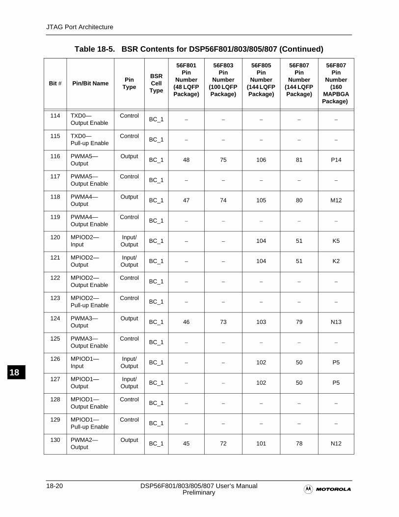
18-20 DSP56F801/803/805/807 User’s Manual�Preliminary
JTAG Port Architecture
ON18
114 TXD0—Output Enable
ControlBC_1 – – – – –
115 TXD0—Pull-up Enable
ControlBC_1 – – – – –
116 PWMA5—Output
OutputBC_1 48 75 106 81 P14
117 PWMA5—Output Enable
ControlBC_1 – – – – –
118 PWMA4—Output
OutputBC_1 47 74 105 80 M12
119 PWMA4—Output Enable
ControlBC_1 – – – – –
120 MPIOD2—Input
Input/Output
BC_1 – – 104 51 K5
121 MPIOD2—Output
Input/Output
BC_1 – – 104 51 K2
122 MPIOD2—Output Enable
ControlBC_1 – – – – –
123 MPIOD2—Pull-up Enable
ControlBC_1 – – – – –
124 PWMA3—Output
OutputBC_1 46 73 103 79 N13
125 PWMA3—Output Enable
ControlBC_1 – – – – –
126 MPIOD1—Input
Input/Output
BC_1 – – 102 50 P5
127 MPIOD1—Output
Input/Output
BC_1 – – 102 50 P5
128 MPIOD1—Output Enable
ControlBC_1 – – – – –
129 MPIOD1—Pull-up Enable
ControlBC_1 – – – – –
130 PWMA2—Output
OutputBC_1 45 72 101 78 N12
Table 18-5. BSR Contents for DSP56F801/803/805/807 (Continued)
Bit # Pin/Bit NamePin
Type
BSR Cell Type
56F801 Pin
Number(48 LQFP Package)
56F803 Pin
Number(100 LQFP Package)
56F805 Pin
Number(144 LQFP Package)
56F807 Pin
Number(144 LQFP Package)
56F807 Pin
Number(160
MAPBGAPackage)
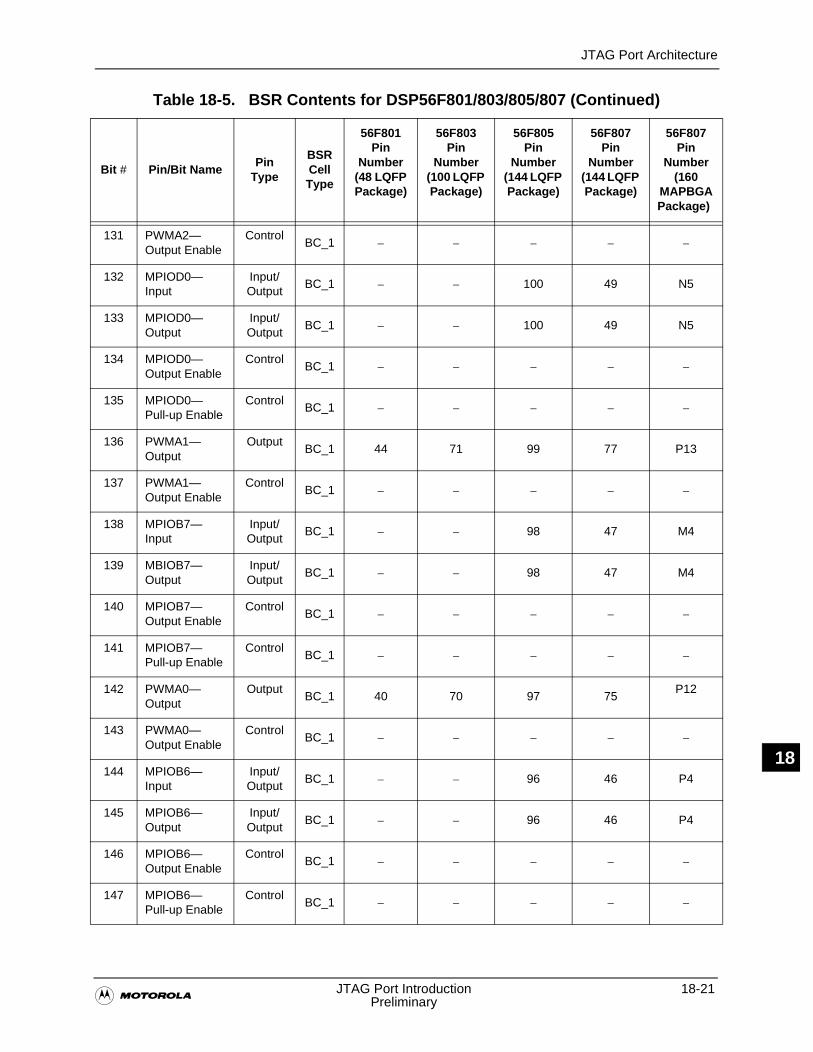
JTAG Port Architecture
�JTAG Port Introduction 18-21
Preliminary
N18
131 PWMA2—Output Enable
ControlBC_1 – – – – –
132 MPIOD0—Input
Input/Output
BC_1 – – 100 49 N5
133 MPIOD0—Output
Input/Output
BC_1 – – 100 49 N5
134 MPIOD0—Output Enable
ControlBC_1 – – – – –
135 MPIOD0—Pull-up Enable
ControlBC_1 – – – – –
136 PWMA1—Output
OutputBC_1 44 71 99 77 P13
137 PWMA1—Output Enable
ControlBC_1 – – – – –
138 MPIOB7—Input
Input/Output
BC_1 – – 98 47 M4
139 MBIOB7—Output
Input/Output
BC_1 – – 98 47 M4
140 MPIOB7—Output Enable
ControlBC_1 – – – – –
141 MPIOB7—Pull-up Enable
ControlBC_1 – – – – –
142 PWMA0—Output
OutputBC_1 40 70 97 75
P12
143 PWMA0—Output Enable
ControlBC_1 – – – – –
144 MPIOB6—Input
Input/Output
BC_1 – – 96 46 P4
145 MPIOB6—Output
Input/Output
BC_1 – – 96 46 P4
146 MPIOB6—Output Enable
ControlBC_1 – – – – –
147 MPIOB6—Pull-up Enable
ControlBC_1 – – – – –
Table 18-5. BSR Contents for DSP56F801/803/805/807 (Continued)
Bit # Pin/Bit NamePin
Type
BSR Cell Type
56F801 Pin
Number(48 LQFP Package)
56F803 Pin
Number(100 LQFP Package)
56F805 Pin
Number(144 LQFP Package)
56F807 Pin
Number(144 LQFP Package)
56F807 Pin
Number(160
MAPBGAPackage)
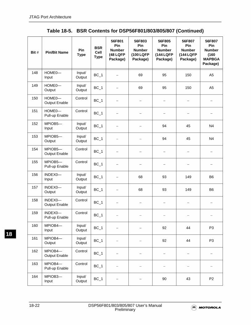
18-22 DSP56F801/803/805/807 User’s Manual�Preliminary
JTAG Port Architecture
ON18
148 HOME0—Input
Input/Output
BC_1 – 69 95 150 A5
149 HOME0—Output
Input/Output
BC_1 – 69 95 150 A5
150 HOME0—Output Enable
ControlBC_1 – – – – –
151 HOME0—Pull-up Enable
ControlBC_1 – – – – –
152 MPIOB5—Input
Input/Output
BC_1 – – 94 45 N4
153 MPIOB5—Output
Input/Output
BC_1 – – 94 45 N4
154 MPIOB5—Output Enable
ControlBC_1 – – – – –
155 MPIOB5—Pull-up Enable
ControlBC_1 – – – – –
156 INDEX0—Input
Input/Output
BC_1 – 68 93 149 B6
157 INDEX0—Output
Input/Output
BC_1 – 68 93 149 B6
158 INDEX0—Output Enable
ControlBC_1 – – – – –
159 INDEX0—Pull-up Enable
ControlBC_1 – – – – –
160 MPIOB4—Input
Input/Output
BC_1 – – 92 44 P3
161 MPIOB4—Output
Input/Output
BC_1 – – 92 44 P3
162 MPIOB4—Output Enable
ControlBC_1 – – – – –
163 MPIOB4—Pull-up Enable
ControlBC_1 – – – – –
164 MPIOB3—Input
Input/Output
BC_1 – – 90 43 P2
Table 18-5. BSR Contents for DSP56F801/803/805/807 (Continued)
Bit # Pin/Bit NamePin
Type
BSR Cell Type
56F801 Pin
Number(48 LQFP Package)
56F803 Pin
Number(100 LQFP Package)
56F805 Pin
Number(144 LQFP Package)
56F807 Pin
Number(144 LQFP Package)
56F807 Pin
Number(160
MAPBGAPackage)
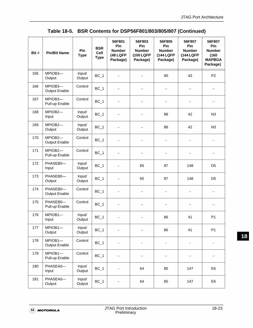
JTAG Port Architecture
�JTAG Port Introduction 18-23
Preliminary
N18
165 MPIOB3—Output
Input/Output
BC_1 – – 90 43 P2
166 MPIOB3—Output Enable
ControlBC_1 – – – – –
167 MPIOB3—Pull-up Enable
ControlBC_1 – – – – –
168 MPIOB2—Input
Input/Output
BC_1 – – 88 42 N3
169 MPIOB2—Output
Input/Output
BC_1 – – 88 42 N3
170 MPIOB2—Output Enable
ControlBC_1 – – – – –
171 MPIOB2—Pull-up Enable
ControlBC_1 – – – – –
172 PHASEB0—Input
Input/Output
BC_1 – 65 87 148 D5
173 PHASEB0—Output
Input/Output
BC_1 – 65 87 148 D5
174 PHASEB0—Output Enable
ControlBC_1 – – – – –
175 PHASEB0—Pull-up Enable
ControlBC_1 – – – – –
176 MPIOB1—Input
Input/Output
BC_1 – – 86 41 P1
177 MPIOB1—Output
Input/Output
BC_1 – – 86 41 P1
178 MPIOB1—Output Enable
ControlBC_1 – – – – –
179 MPIOB1—Pull-up Enable
ControlBC_1 – – – – –
180 PHASEA0—Input
Input/Output
BC_1 – 64 85 147 E6
181 PHASEA0—Output
Input/Output
BC_1 – 64 85 147 E6
Table 18-5. BSR Contents for DSP56F801/803/805/807 (Continued)
Bit # Pin/Bit NamePin
Type
BSR Cell Type
56F801 Pin
Number(48 LQFP Package)
56F803 Pin
Number(100 LQFP Package)
56F805 Pin
Number(144 LQFP Package)
56F807 Pin
Number(144 LQFP Package)
56F807 Pin
Number(160
MAPBGAPackage)
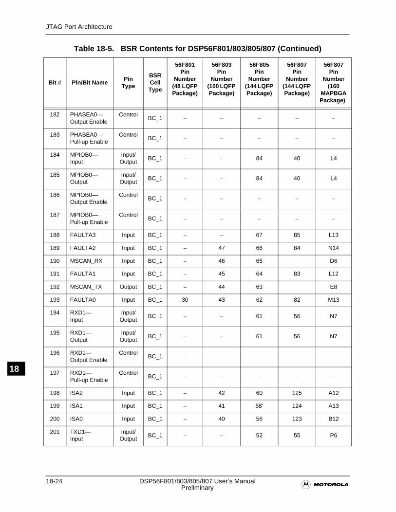
18-24 DSP56F801/803/805/807 User’s Manual�Preliminary
JTAG Port Architecture
ON18
182 PHASEA0—Output Enable
ControlBC_1 – – – – –
183 PHASEA0—Pull-up Enable
ControlBC_1 – – – – –
184 MPIOB0—Input
Input/Output
BC_1 – – 84 40 L4
185 MPIOB0—Output
Input/Output
BC_1 – – 84 40 L4
186 MPIOB0—Output Enable
ControlBC_1 – – – – –
187 MPIOB0—Pull-up Enable
ControlBC_1 – – – – –
188 FAULTA3 Input BC_1 – – 67 85 L13
189 FAULTA2 Input BC_1 – 47 66 84 N14
190 MSCAN_RX Input BC_1 – 46 65 D6
191 FAULTA1 Input BC_1 – 45 64 83 L12
192 MSCAN_TX Output BC_1 – 44 63 E8
193 FAULTA0 Input BC_1 30 43 62 82 M13
194 RXD1—Input
Input/Output
BC_1 – – 61 56 N7
195 RXD1—Output
Input/Output
BC_1 – – 61 56 N7
196 RXD1—Output Enable
ControlBC_1 – – – – –
197 RXD1—Pull-up Enable
ControlBC_1 – – – – –
198 ISA2 Input BC_1 – 42 60 125 A12
199 ISA1 Input BC_1 – 41 58‘ 124 A13
200 ISA0 Input BC_1 – 40 56 123 B12
201 TXD1—Input
Input/Output
BC_1 – – 52 55 P6
Table 18-5. BSR Contents for DSP56F801/803/805/807 (Continued)
Bit # Pin/Bit NamePin
Type
BSR Cell Type
56F801 Pin
Number(48 LQFP Package)
56F803 Pin
Number(100 LQFP Package)
56F805 Pin
Number(144 LQFP Package)
56F807 Pin
Number(144 LQFP Package)
56F807 Pin
Number(160
MAPBGAPackage)
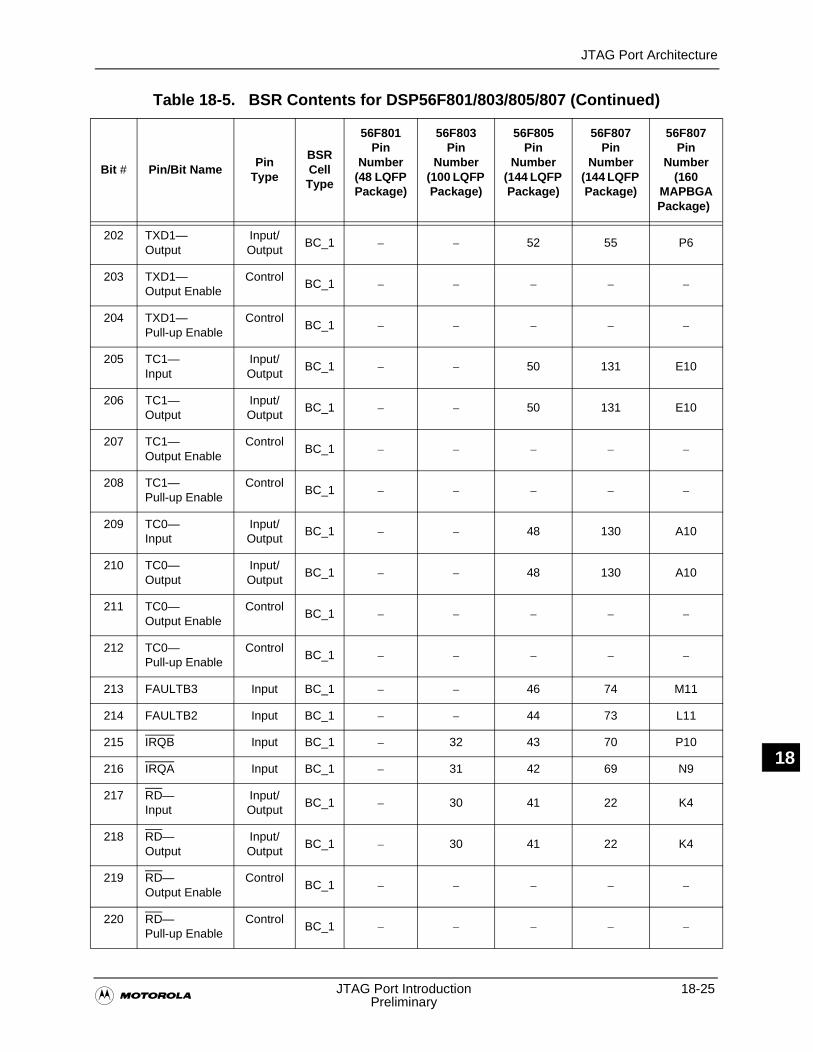
JTAG Port Architecture
�JTAG Port Introduction 18-25
Preliminary
N18
202 TXD1—Output
Input/Output
BC_1 – – 52 55 P6
203 TXD1—Output Enable
ControlBC_1 – – – – –
204 TXD1—Pull-up Enable
ControlBC_1 – – – – –
205 TC1—Input
Input/Output
BC_1 – – 50 131 E10
206 TC1—Output
Input/Output
BC_1 – – 50 131 E10
207 TC1—Output Enable
ControlBC_1 – – – – –
208 TC1—Pull-up Enable
ControlBC_1 – – – – –
209 TC0—Input
Input/Output
BC_1 – – 48 130 A10
210 TC0—Output
Input/Output
BC_1 – – 48 130 A10
211 TC0—Output Enable
ControlBC_1 – – – – –
212 TC0—Pull-up Enable
ControlBC_1 – – – – –
213 FAULTB3 Input BC_1 – – 46 74 M11
214 FAULTB2 Input BC_1 – – 44 73 L11
215 IRQB Input BC_1 – 32 43 70 P10
216 IRQA Input BC_1 – 31 42 69 N9
217 RD—Input
Input/Output
BC_1 – 30 41 22 K4
218 RD—Output
Input/Output
BC_1 – 30 41 22 K4
219 RD—Output Enable
ControlBC_1 – – – – –
220 RD—Pull-up Enable
ControlBC_1 – – – – –
Table 18-5. BSR Contents for DSP56F801/803/805/807 (Continued)
Bit # Pin/Bit NamePin
Type
BSR Cell Type
56F801 Pin
Number(48 LQFP Package)
56F803 Pin
Number(100 LQFP Package)
56F805 Pin
Number(144 LQFP Package)
56F807 Pin
Number(144 LQFP Package)
56F807 Pin
Number(160
MAPBGAPackage)

18-26 DSP56F801/803/805/807 User’s Manual�Preliminary
JTAG Port Architecture
ON18
221 WR—Input
Input/Output
BC_1 – 29 40 21 J4
222 WR—Output
Input/Output
BC_1 – 29 40 21 J4
223 WR—Output Enable
ControlBC_1 – – – – –
224 WR—Pull-up Enable
ControlBC_1 – – – – –
225 A15—Input
Input/Output
BC_1 – 27 38 17 G1
226 A15—Output
Input/Output
BC_1 – 27 38 17 G1
227 A15—Output Enable
ControlBC_1 – – – – –
228 A15—Pull-up Enable
ControlBC_1 – – – – –
229 A14—Input
Input/Output
BC_1 – 26 37 16 G2
230 A14—Output
Input/Output
BC_1 – 26 37 16 G2
231 A14—Output Enable
ControlBC_1 – – – – –
232 A14—Pull-up Enable
ControlBC_1 – – – – –
233 DS—Input
Input/Output
BC_1 – 25 36 20 H4
234 DS—Output
Input/Output
BC_1 – 25 36 20 H4
235 DS—Output Enable
ControlBC_1 – – – – –
236 DS—Pull-up Enable
ControlBC_1 – – – – –
237 PS—Input
Input/Output
BC_1 – 24 35 19 G4
Table 18-5. BSR Contents for DSP56F801/803/805/807 (Continued)
Bit # Pin/Bit NamePin
Type
BSR Cell Type
56F801 Pin
Number(48 LQFP Package)
56F803 Pin
Number(100 LQFP Package)
56F805 Pin
Number(144 LQFP Package)
56F807 Pin
Number(144 LQFP Package)
56F807 Pin
Number(160
MAPBGAPackage)
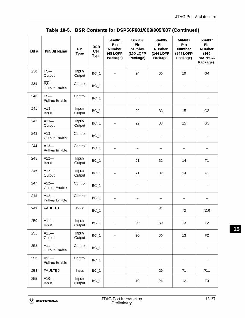
JTAG Port Architecture
�JTAG Port Introduction 18-27
Preliminary
N18
238 PS—Output
Input/Output
BC_1 – 24 35 19 G4
239 PS—Output Enable
ControlBC_1 – – – – –
240 PS—Pull-up Enable
ControlBC_1 – – – – –
241 A13—Input
Input/Output
BC_1 – 22 33 15 G3
242 A13—Output
Input/Output
BC_1 – 22 33 15 G3
243 A13—Output Enable
ControlBC_1 – – – – –
244 A13—Pull-up Enable
ControlBC_1 – – – – –
245 A12—Input
Input/Output
BC_1 – 21 32 14 F1
246 A12—Output
Input/Output
BC_1 – 21 32 14 F1
247 A12—Output Enable
ControlBC_1 – – – – –
248 A12—Pull-up Enable
ControlBC_1 – – – – –
249 FAULTB1 InputBC_1 – –
3172 N10
250 A11—Input
Input/Output
BC_1 – 20 30 13 F2
251 A11—Output
Input/Output
BC_1 – 20 30 13 F2
252 A11—Output Enable
ControlBC_1 – – – – –
253 A11—Pull-up Enable
ControlBC_1 – – – – –
254 FAULTB0 Input BC_1 – – 29 71 P11
255 A10—Input
Input/Output
BC_1 – 19 28 12 F3
Table 18-5. BSR Contents for DSP56F801/803/805/807 (Continued)
Bit # Pin/Bit NamePin
Type
BSR Cell Type
56F801 Pin
Number(48 LQFP Package)
56F803 Pin
Number(100 LQFP Package)
56F805 Pin
Number(144 LQFP Package)
56F807 Pin
Number(144 LQFP Package)
56F807 Pin
Number(160
MAPBGAPackage)
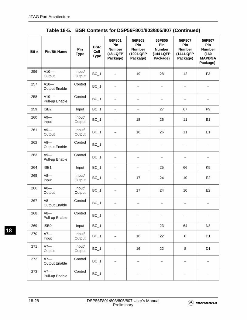
18-28 DSP56F801/803/805/807 User’s Manual�Preliminary
JTAG Port Architecture
ON18
256 A10—Output
Input/Output
BC_1 – 19 28 12 F3
257 A10—Output Enable
ControlBC_1 – – – – –
258 A10—Pull-up Enable
ControlBC_1 – – – – –
259 ISB2 Input BC_1 – – 27 67 P9
260 A9—Input
Input/Output
BC_1 – 18 26 11 E1
261 A9—Output
Input/Output
BC_1 – 18 26 11 E1
262 A9—Output Enable
ControlBC_1 – – – – –
263 A9—Pull-up Enable
ControlBC_1 – – – – –
264 ISB1 Input BC_1 – – 25 66 K9
265 A8—Input
Input/Output
BC_1 – 17 24 10 E2
266 A8—Output
Input/Output
BC_1 – 17 24 10 E2
267 A8—Output Enable
ControlBC_1 – – – – –
268 A8—Pull-up Enable
ControlBC_1 – – – – –
269 ISB0 Input BC_1 – – 23 64 N8
270 A7—Input
Input/Output
BC_1 – 16 22 8 D1
271 A7—Output
Input/Output
BC_1 – 16 22 8 D1
272 A7—Output Enable
ControlBC_1 – – – – –
273 A7—Pull-up Enable
ControlBC_1 – – – – –
Table 18-5. BSR Contents for DSP56F801/803/805/807 (Continued)
Bit # Pin/Bit NamePin
Type
BSR Cell Type
56F801 Pin
Number(48 LQFP Package)
56F803 Pin
Number(100 LQFP Package)
56F805 Pin
Number(144 LQFP Package)
56F807 Pin
Number(144 LQFP Package)
56F807 Pin
Number(160
MAPBGAPackage)
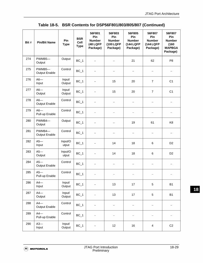
JTAG Port Architecture
�JTAG Port Introduction 18-29
Preliminary
N18
274 PWMB5—Output
OutputBC_1 – – 21 62 P8
275 PWMB5—Output Enable
ControlBC_1 – – – – –
276 A6—Input
Input/Output
BC_1 – 15 20 7 C1
277 A6—Output
Input/Output
BC_1 – 15 20 7 C1
278 A6—Output Enable
ControlBC_1 – – – – –
279 A6—Pull-up Enable
ControlBC_1 – – – – –
280 PWMB4—Output
OutputBC_1 – – 19 61 K8
281 PWMB4—Output Enable
ControlBC_1 – – – – –
282 A5—Input
Input/Output
BC_1 – 14 18 6 D2
283 A5—Output
Input/Output
BC_1 – 14 18 6 D2
284 A5—Output Enable
ControlBC_1 – – – – –
285 A5—Pull-up Enable
ControlBC_1 – – – – –
286 A4—Input
Input/Output
BC_1 – 13 17 5 B1
287 A4—Output
Input/Output
BC_1 – 13 17 5 B1
288 A4—Output Enable
ControlBC_1 – – – – –
289 A4—Pull-up Enable
ControlBC_1 – – – – –
290 A3—Input
Input/Output
BC_1 – 12 16 4 C2
Table 18-5. BSR Contents for DSP56F801/803/805/807 (Continued)
Bit # Pin/Bit NamePin
Type
BSR Cell Type
56F801 Pin
Number(48 LQFP Package)
56F803 Pin
Number(100 LQFP Package)
56F805 Pin
Number(144 LQFP Package)
56F807 Pin
Number(144 LQFP Package)
56F807 Pin
Number(160
MAPBGAPackage)
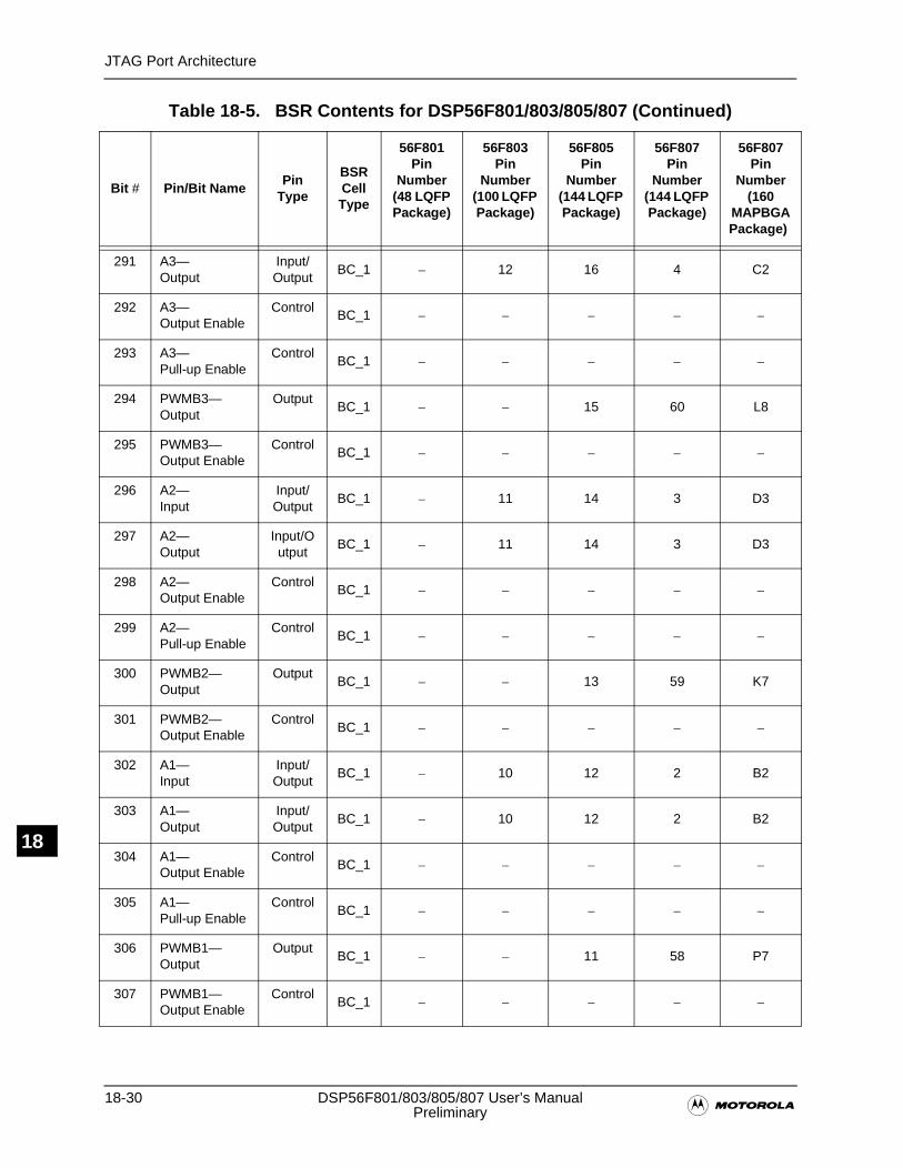
18-30 DSP56F801/803/805/807 User’s Manual�Preliminary
JTAG Port Architecture
ON18
291 A3—Output
Input/Output
BC_1 – 12 16 4 C2
292 A3—Output Enable
ControlBC_1 – – – – –
293 A3—Pull-up Enable
ControlBC_1 – – – – –
294 PWMB3—Output
OutputBC_1 – – 15 60 L8
295 PWMB3—Output Enable
ControlBC_1 – – – – –
296 A2—Input
Input/Output
BC_1 – 11 14 3 D3
297 A2—Output
Input/Output
BC_1 – 11 14 3 D3
298 A2—Output Enable
ControlBC_1 – – – – –
299 A2—Pull-up Enable
ControlBC_1 – – – – –
300 PWMB2—Output
OutputBC_1 – – 13 59 K7
301 PWMB2—Output Enable
ControlBC_1 – – – – –
302 A1—Input
Input/Output
BC_1 – 10 12 2 B2
303 A1—Output
Input/Output
BC_1 – 10 12 2 B2
304 A1—Output Enable
ControlBC_1 – – – – –
305 A1—Pull-up Enable
ControlBC_1 – – – – –
306 PWMB1—Output
OutputBC_1 – – 11 58 P7
307 PWMB1—Output Enable
ControlBC_1 – – – – –
Table 18-5. BSR Contents for DSP56F801/803/805/807 (Continued)
Bit # Pin/Bit NamePin
Type
BSR Cell Type
56F801 Pin
Number(48 LQFP Package)
56F803 Pin
Number(100 LQFP Package)
56F805 Pin
Number(144 LQFP Package)
56F807 Pin
Number(144 LQFP Package)
56F807 Pin
Number(160
MAPBGAPackage)

JTAG Port Architecture
�JTAG Port Introduction 18-31
Preliminary
N18
308 PWMB0—Output
OutputBC_1 – – 9 57 L7
309 PWMB0—Output Enable
ControlBC_1 – – – – –
310 A0—Input
Input/Output
BC_1 – 7 7 1 C3
311 A0—Output
Input/Output
BC_1 – 7 7 1 C3
312 A0—Output Enable
ControlBC_1 – – – – –
313 A0—Pull-up Enable
ControlBC_1 – – – – –
314 D15—Input
Input/Output
BC_1 – 6 6 39 M3
315 D15—Output
Input/Output
BC_1 – 6 6 39 M3
316 D15—Output Enable
ControlBC_1 – – – – –
317 D15—Pull-up Enable
ControlBC_1 – – – – –
318 D14—Input
Input/Output
BC_1 – 5 5 38 N2
319 D14—Output
Input/Output
BC_1 – 5 5 38 N2
320 D14—Output Enable
ControlBC_1 – – – – –
321 D14—Pull-up Enable
ControlBC_1 – – – – –
322 D13—Input
Input/Output
BC_1 – 4 4 37 M2
323 D13—Output
Input/Output
BC_1 – 4 4 37 M2
324 D13—Output Enable
ControlBC_1 – – – – –
Table 18-5. BSR Contents for DSP56F801/803/805/807 (Continued)
Bit # Pin/Bit NamePin
Type
BSR Cell Type
56F801 Pin
Number(48 LQFP Package)
56F803 Pin
Number(100 LQFP Package)
56F805 Pin
Number(144 LQFP Package)
56F807 Pin
Number(144 LQFP Package)
56F807 Pin
Number(160
MAPBGAPackage)
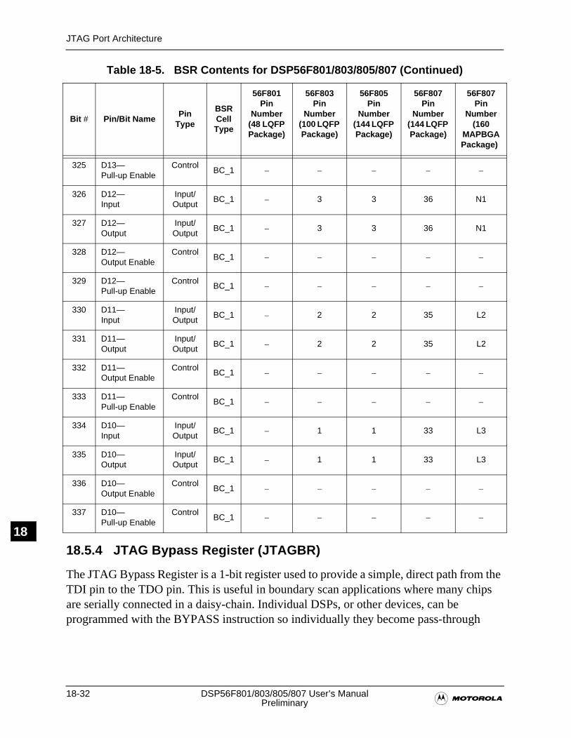
18-32 DSP56F801/803/805/807 User’s Manual�Preliminary
JTAG Port Architecture
ON18
18.5.4 JTAG Bypass Register (JTAGBR)
The JTAG Bypass Register is a 1-bit register used to provide a simple, direct path from the TDI pin to the TDO pin. This is useful in boundary scan applications where many chips are serially connected in a daisy-chain. Individual DSPs, or other devices, can be programmed with the BYPASS instruction so individually they become pass-through
325 D13—Pull-up Enable
ControlBC_1 – – – – –
326 D12—Input
Input/Output
BC_1 – 3 3 36 N1
327 D12—Output
Input/Output
BC_1 – 3 3 36 N1
328 D12—Output Enable
ControlBC_1 – – – – –
329 D12—Pull-up Enable
ControlBC_1 – – – – –
330 D11—Input
Input/Output
BC_1 – 2 2 35 L2
331 D11—Output
Input/Output
BC_1 – 2 2 35 L2
332 D11—Output Enable
ControlBC_1 – – – – –
333 D11—Pull-up Enable
ControlBC_1 – – – – –
334 D10—Input
Input/Output
BC_1 – 1 1 33 L3
335 D10—Output
Input/Output
BC_1 – 1 1 33 L3
336 D10—Output Enable
ControlBC_1 – – – – –
337 D10—Pull-up Enable
ControlBC_1 – – – – –
Table 18-5. BSR Contents for DSP56F801/803/805/807 (Continued)
Bit # Pin/Bit NamePin
Type
BSR Cell Type
56F801 Pin
Number(48 LQFP Package)
56F803 Pin
Number(100 LQFP Package)
56F805 Pin
Number(144 LQFP Package)
56F807 Pin
Number(144 LQFP Package)
56F807 Pin
Number(160
MAPBGAPackage)
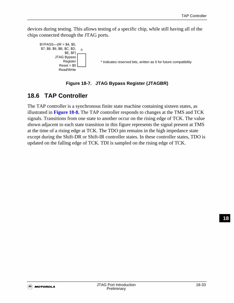
TAP Controller
�JTAG Port Introduction 18-33
Preliminary
N18
devices during testing. This allows testing of a specific chip, while still having all of the chips connected through the JTAG ports.
Figure 18-7. JTAG Bypass Register (JTAGBR)
18.6 TAP Controller
The TAP controller is a synchronous finite state machine containing sixteen states, as illustrated in Figure 18-8. The TAP controller responds to changes at the TMS and TCK signals. Transitions from one state to another occur on the rising edge of TCK. The value shown adjacent to each state transition in this figure represents the signal present at TMS at the time of a rising edge at TCK. The TDO pin remains in the high impedance state except during the Shift-DR or Shift-IR controller states. In these controller states, TDO is updated on the falling edge of TCK. TDI is sampled on the rising edge of TCK.
* Indicates reserved bits, written as 0 for future compatibility
BYPASS—(IR = $4, $5,$7, $8, $9, $B, $C, $D,
$E, $F)JTAG Bypass
RegisterReset = $0Read/Write
0
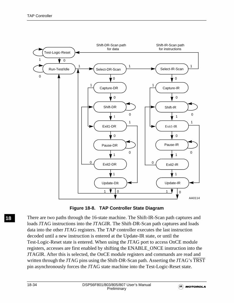
18-34 DSP56F801/803/805/807 User’s Manual�Preliminary
TAP Controller
ON18 There are two paths through the 16-state machine. The Shift-IR-Scan path captures and loads JTAG instructions into the JTAGIR. The Shift-DR-Scan path captures and loads data into the other JTAG registers. The TAP controller executes the last instruction decoded until a new instruction is entered at the Update-IR state, or until the Test-Logic-Reset state is entered. When using the JTAG port to access OnCE module registers, accesses are first enabled by shifting the ENABLE_ONCE instruction into the JTAGIR. After this is selected, the OnCE module registers and commands are read and written through the JTAG pins using the Shift-DR-Scan path. Asserting the JTAG’s TRST pin asynchronously forces the JTAG state machine into the Test-Logic-Reset state.
Figure 18-8. TAP Controller State Diagram
Select-DR-Scan
Capture-DR
Shift-DR
Exit1-DR
Pause-DR
Exit2-DR
Test-Logic-Reset
Run-Test/Idle
Update-DR
1
0
0
1
0
1
1
0
1
1
0
0
1 0
Select-IR-Scan
Capture-IR
Shift-IR
Exit1-IR
Pause-IR
Exit2-IR
Update-IR
0
0
1
0
1
1
0
1
1
0
0
1 0
01
0
1 1
AA0114
Shift-DR-Scan pathfor data
Shift-IR-Scan pathfor instructions
DSP56F801/803/805/807 Restrictions
�JTAG Port Introduction 18-35
Preliminary
N18
18.7 DSP56F801/803/805/807 Restrictions
The control afforded by the output enable signals using the BSR and the EXTEST instruction requires a compatible circuit board test environment to avoid any device-destructive configurations. Avoid situations when the DSP56F801/803/805/807 output drivers are enabled into actively driven networks.
During power-up, the TRST pin must be externally asserted to force the TAP controller into this state. After power-up is concluded, TMS must be sampled as a logic one for five consecutive TCK rising edges. If TMS either remains unconnected or is connected to VDD, then the TAP controller cannot leave the Test-Logic-Reset state, regardless of the state of TCK.
DSP56F801/803/805/807 features a low-power Stop Mode invoked using the STOP instruction. JTAG interaction with low-power Stop Mode is as follows:
1. The TAP controller must be in the Test-Logic-Reset state to either enter or remain in Stop Mode. Leaving the TAP controller Test-Logic-Reset state negates the ability to achieve low-power, but does not otherwise affect device functionality
2. The TCK input is not blocked in low-power Stop Mode. To consume minimal power, the TCK input should be externally connected to VDD or ground
3. The TMS and TDI pins include on-chip pull-up resistors. In low-power Stop Mode, these two pins should remain either unconnected or connected to VDD to achieve minimal power consumption
Because all DSP56F801/803/805/807 clocks are disabled during Stop state, the JTAG interface provides the means of polling the device status, sampled in the Capture-IR state.
18-36 DSP56F801/803/805/807 User’s Manual�Preliminary
DSP56F801/803/805/807 Restrictions
ON18

�Appendix A - Glossary A-1
Preliminary
A
Appendix AGlossary

A-2 DSP58603/05 User’s Manual�Preliminary
A

�Appendix A - Glossary A-3
Preliminary
A
A.1 GlossaryThis glossary is intended to reduce confusion that may be caused by the use of many acronyms and abbreviations throughout this manual.
ACIM A/C Induction Motors
A/D Analog-to-Digital
ADC Analog to Digital Converter
ADCR ADC Control Registe
ADDR Address
ADHLMT ADC High Limit Registers
ADLLMT ADC Low Limit Registers
ADLST ADC Channel List Registers
ADLSTAT ADC Limit Status Register
ADM Application Development Module
ADOFS ADC Offset Registers
ADR PD Address Bus Pull-up Disable
ADRSLT ADC Result Registers
ADSDIS ADC Sample Disable Register
ADSTAT ADC Status Register
ADZCC ADC Zero Crossing Control Register
ADZCSTAT ADC Zero Crossing Status Register
AGU Address Generation Unit
ALU Arithmetic Logic Unit
API Application Program Interface
Barrel Shifter Part of the ALU that allows single cycle shifting and rotating of data word
BCR Bus Control Register
BDC Brush DC Motor
BE Breakpoint Enable
BFIU Boot Flash Interface Unit
BFLASH Boot Flash
BK Breakpoint Configuration Bit
BLDC Brushless DC Motor
BOTNEG Bottom-side PWM Polarity Bit
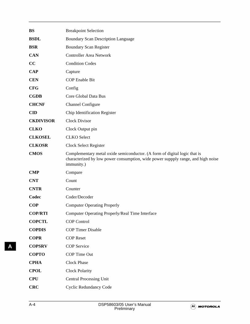
A-4 DSP58603/05 User’s Manual�Preliminary
A
BS Breakpoint Selection
BSDL Boundary Scan Description Language
BSR Boundary Scan Register
CAN Controller Area Network
CC Condition Codes
CAP Capture
CEN COP Enable Bit
CFG Config
CGDB Core Global Data Bus
CHCNF Channel Configure
CID Chip Identification Register
CKDIVISOR Clock Divisor
CLKO Clock Output pin
CLKOSEL CLKO Select
CLKOSR Clock Select Register
CMOS Complementary metal oxide semiconductor. (A form of digital logic that is characterized by low power consumption, wide power suppply range, and high noise immunity.)
CMP Compare
CNT Count
CNTR Counter
Codec Coder/Decoder
COP Computer Operating Properly
COP/RTI Computer Operating Properly/Real Time Interface
COPCTL COP Control
COPDIS COP Timer Disable
COPR COP Reset
COPSRV COP Service
COPTO COP Time Out
CPHA Clock Phase
CPOL Clock Polarity
CPU Central Processing Unit
CRC Cyclic Redundancy Code
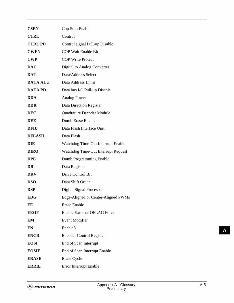
�Appendix A - Glossary A-5
Preliminary
A
CSEN Cop Stop Enable
CTRL Control
CTRL PD Control signal Pull-up Disable
CWEN COP Wait Enable Bit
CWP COP Write Protect
DAC Digital to Analog Converter
DAT Data/Address Select
DATA ALU Data Address Limit
DATA PD Data bus I/O Pull-up Disable
DDA Analog Power
DDR Data Direction Register
DEC Quadrature Decoder Module
DEE Dumb Erase Enable
DFIU Data Flash Interface Unit
DFLASH Data Flash
DIE Watchdog Time-Out Interrupt Enable
DIRQ Watchdog Time-Out Interrupt Request
DPE Dumb Programming Enable
DR Data Register
DRV Drive Control Bit
DSO Data Shift Order
DSP Digital Signal Processor
EDG Edge-Aligned or Center-Aligned PWMs
EE Erase Enable
EEOF Enable External OFLAG Force
EM Event Modifier
EN Enable3
ENCR Encoder Control Register
EOSI End of Scan Interrupt
EOSIE End of Scan Interrupt Enable
ERASE Erase Cycle
ERRIE Error Interrupt Enable
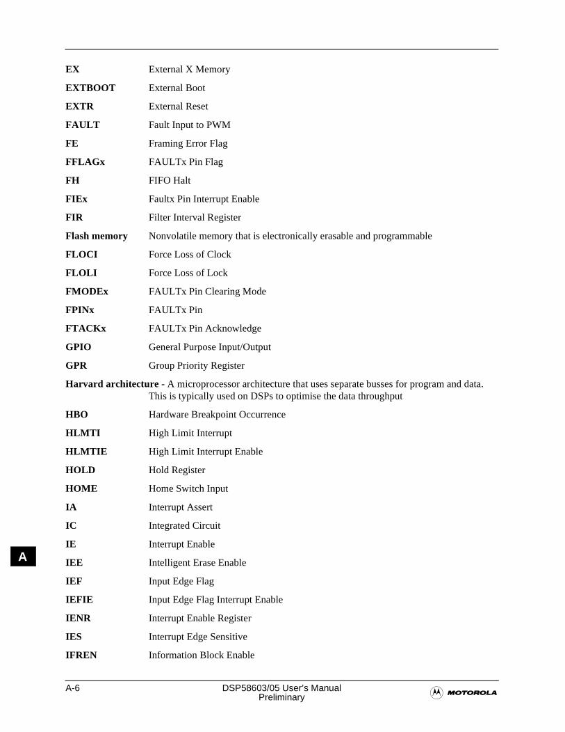
A-6 DSP58603/05 User’s Manual�Preliminary
A
EX External X Memory
EXTBOOT External Boot
EXTR External Reset
FAULT Fault Input to PWM
FE Framing Error Flag
FFLAGx FAULTx Pin Flag
FH FIFO Halt
FIEx Faultx Pin Interrupt Enable
FIR Filter Interval Register
Flash memory Nonvolatile memory that is electronically erasable and programmable
FLOCI Force Loss of Clock
FLOLI Force Loss of Lock
FMODEx FAULTx Pin Clearing Mode
FPINx FAULTx Pin
FTACKx FAULTx Pin Acknowledge
GPIO General Purpose Input/Output
GPR Group Priority Register
Harvard architecture - A microprocessor architecture that uses separate busses for program and data. This is typically used on DSPs to optimise the data throughput
HBO Hardware Breakpoint Occurrence
HLMTI High Limit Interrupt
HLMTIE High Limit Interrupt Enable
HOLD Hold Register
HOME Home Switch Input
IA Interrupt Assert
IC Integrated Circuit
IE Interrupt Enable
IEE Intelligent Erase Enable
IEF Input Edge Flag
IEFIE Input Edge Flag Interrupt Enable
IENR Interrupt Enable Register
IES Interrupt Edge Sensitive
IFREN Information Block Enable
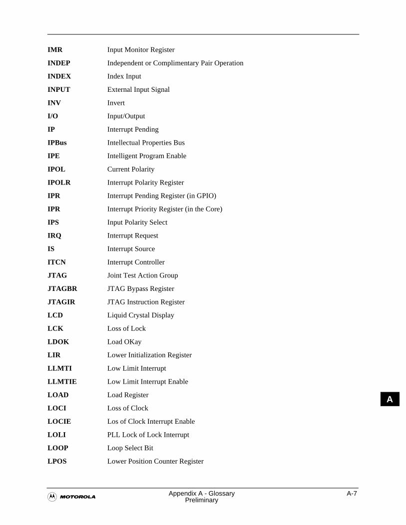
�Appendix A - Glossary A-7
Preliminary
A
IMR Input Monitor Register
INDEP Independent or Complimentary Pair Operation
INDEX Index Input
INPUT External Input Signal
INV Invert
I/O Input/Output
IP Interrupt Pending
IPBus Intellectual Properties Bus
IPE Intelligent Program Enable
IPOL Current Polarity
IPOLR Interrupt Polarity Register
IPR Interrupt Pending Register (in GPIO)
IPR Interrupt Priority Register (in the Core)
IPS Input Polarity Select
IRQ Interrupt Request
IS Interrupt Source
ITCN Interrupt Controller
JTAG Joint Test Action Group
JTAGBR JTAG Bypass Register
JTAGIR JTAG Instruction Register
LCD Liquid Crystal Display
LCK Loss of Lock
LDOK Load OKay
LIR Lower Initialization Register
LLMTI Low Limit Interrupt
LLMTIE Low Limit Interrupt Enable
LOAD Load Register
LOCI Loss of Clock
LOCIE Los of Clock Interrupt Enable
LOLI PLL Lock of Lock Interrupt
LOOP Loop Select Bit
LPOS Lower Position Counter Register
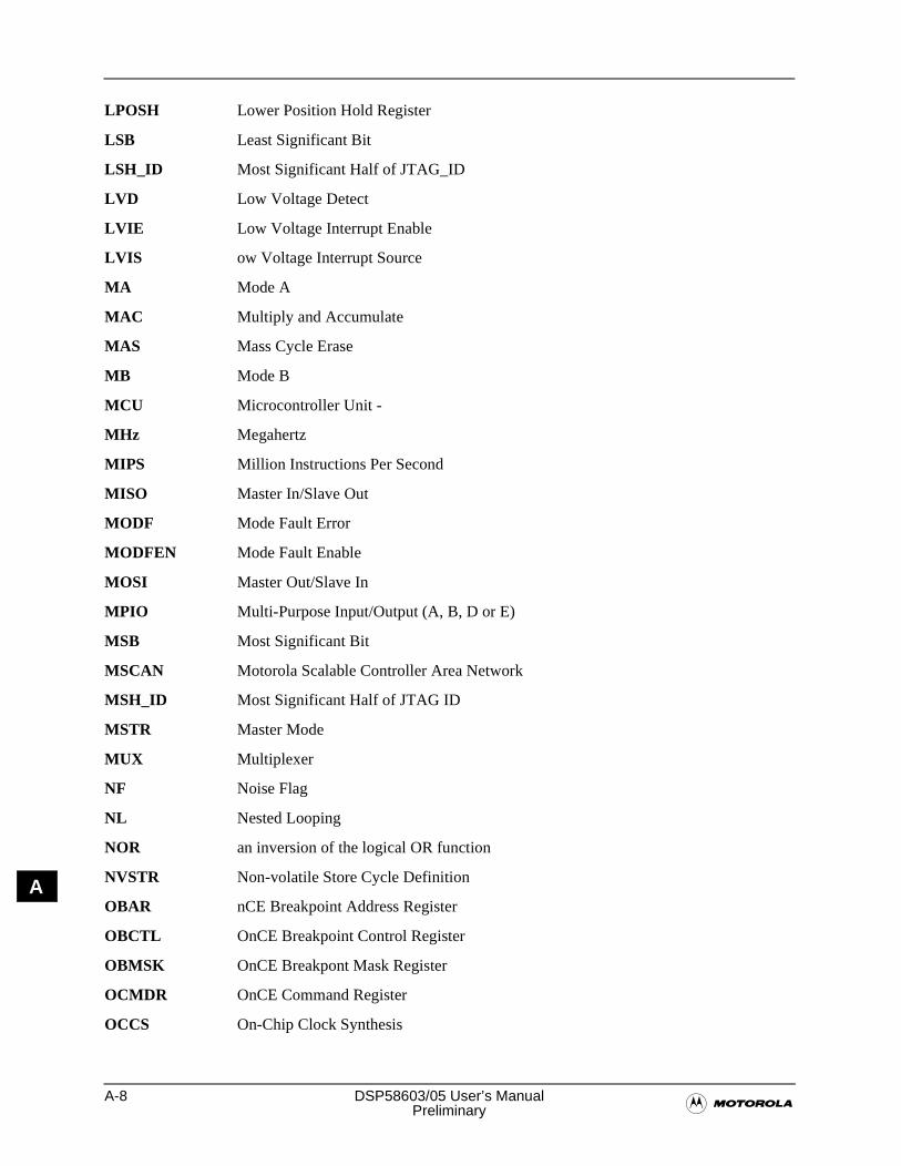
A-8 DSP58603/05 User’s Manual�Preliminary
A
LPOSH Lower Position Hold Register
LSB Least Significant Bit
LSH_ID Most Significant Half of JTAG_ID
LVD Low Voltage Detect
LVIE Low Voltage Interrupt Enable
LVIS ow Voltage Interrupt Source
MA Mode A
MAC Multiply and Accumulate
MAS Mass Cycle Erase
MB Mode B
MCU Microcontroller Unit -
MHz Megahertz
MIPS Million Instructions Per Second
MISO Master In/Slave Out
MODF Mode Fault Error
MODFEN Mode Fault Enable
MOSI Master Out/Slave In
MPIO Multi-Purpose Input/Output (A, B, D or E)
MSB Most Significant Bit
MSCAN Motorola Scalable Controller Area Network
MSH_ID Most Significant Half of JTAG ID
MSTR Master Mode
MUX Multiplexer
NF Noise Flag
NL Nested Looping
NOR an inversion of the logical OR function
NVSTR Non-volatile Store Cycle Definition
OBAR nCE Breakpoint Address Register
OBCTL OnCE Breakpoint Control Register
OBMSK OnCE Breakpont Mask Register
OCMDR OnCE Command Register
OCCS On-Chip Clock Synthesis
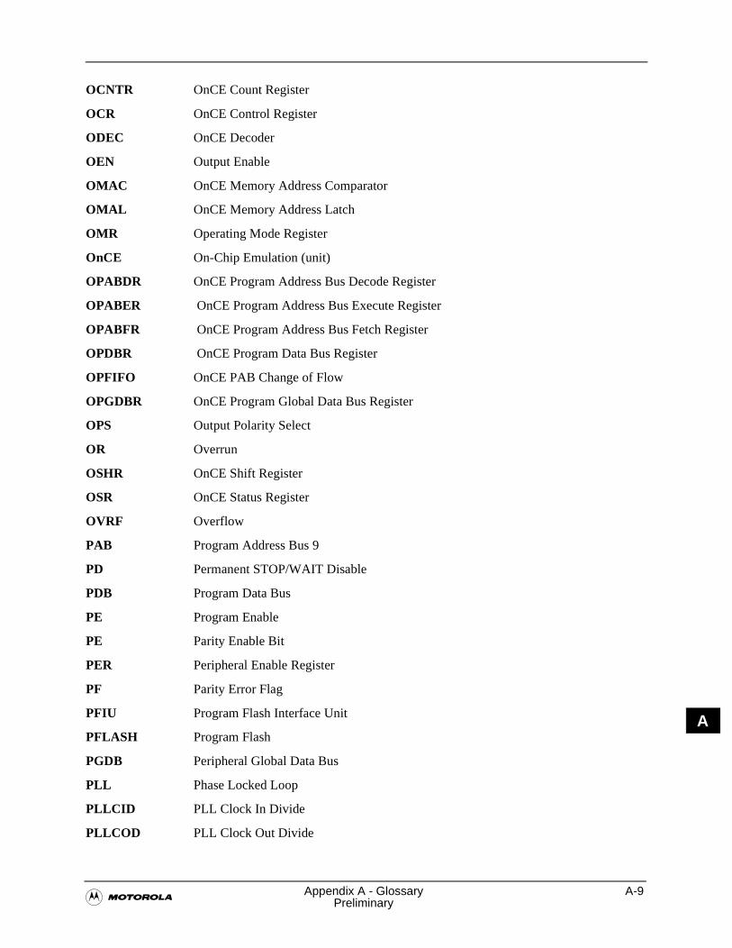
�Appendix A - Glossary A-9
Preliminary
A
OCNTR OnCE Count Register
OCR OnCE Control Register
ODEC OnCE Decoder
OEN Output Enable
OMAC OnCE Memory Address Comparator
OMAL OnCE Memory Address Latch
OMR Operating Mode Register
OnCE On-Chip Emulation (unit)
OPABDR OnCE Program Address Bus Decode Register
OPABER OnCE Program Address Bus Execute Register
OPABFR OnCE Program Address Bus Fetch Register
OPDBR OnCE Program Data Bus Register
OPFIFO OnCE PAB Change of Flow
OPGDBR OnCE Program Global Data Bus Register
OPS Output Polarity Select
OR Overrun
OSHR OnCE Shift Register
OSR OnCE Status Register
OVRF Overflow
PAB Program Address Bus 9
PD Permanent STOP/WAIT Disable
PDB Program Data Bus
PE Program Enable
PE Parity Enable Bit
PER Peripheral Enable Register
PF Parity Error Flag
PFIU Program Flash Interface Unit
PFLASH Program Flash
PGDB Peripheral Global Data Bus
PLL Phase Locked Loop
PLLCID PLL Clock In Divide
PLLCOD PLL Clock Out Divide
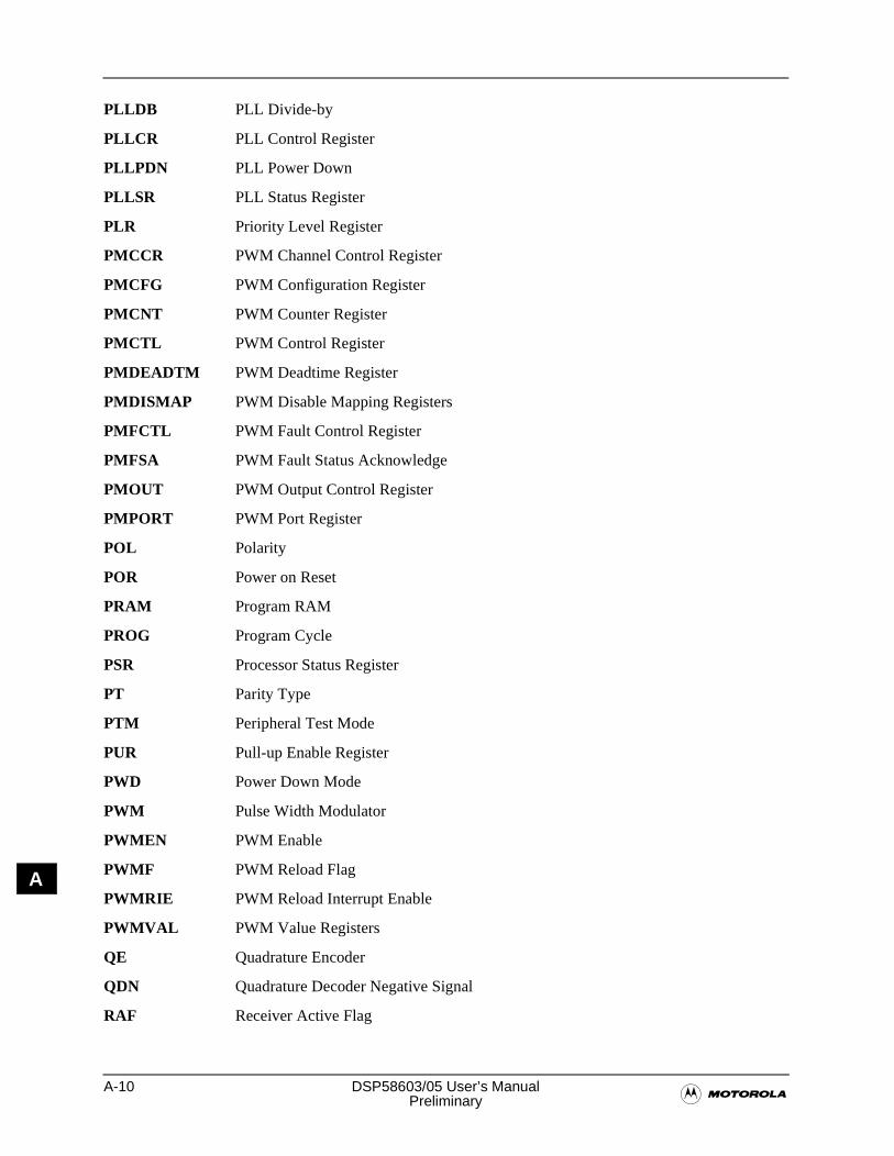
A-10 DSP58603/05 User’s Manual�Preliminary
A
PLLDB PLL Divide-by
PLLCR PLL Control Register
PLLPDN PLL Power Down
PLLSR PLL Status Register
PLR Priority Level Register
PMCCR PWM Channel Control Register
PMCFG PWM Configuration Register
PMCNT PWM Counter Register
PMCTL PWM Control Register
PMDEADTM PWM Deadtime Register
PMDISMAP PWM Disable Mapping Registers
PMFCTL PWM Fault Control Register
PMFSA PWM Fault Status Acknowledge
PMOUT PWM Output Control Register
PMPORT PWM Port Register
POL Polarity
POR Power on Reset
PRAM Program RAM
PROG Program Cycle
PSR Processor Status Register
PT Parity Type
PTM Peripheral Test Mode
PUR Pull-up Enable Register
PWD Power Down Mode
PWM Pulse Width Modulator
PWMEN PWM Enable
PWMF PWM Reload Flag
PWMRIE PWM Reload Interrupt Enable
PWMVAL PWM Value Registers
QE Quadrature Encoder
QDN Quadrature Decoder Negative Signal
RAF Receiver Active Flag
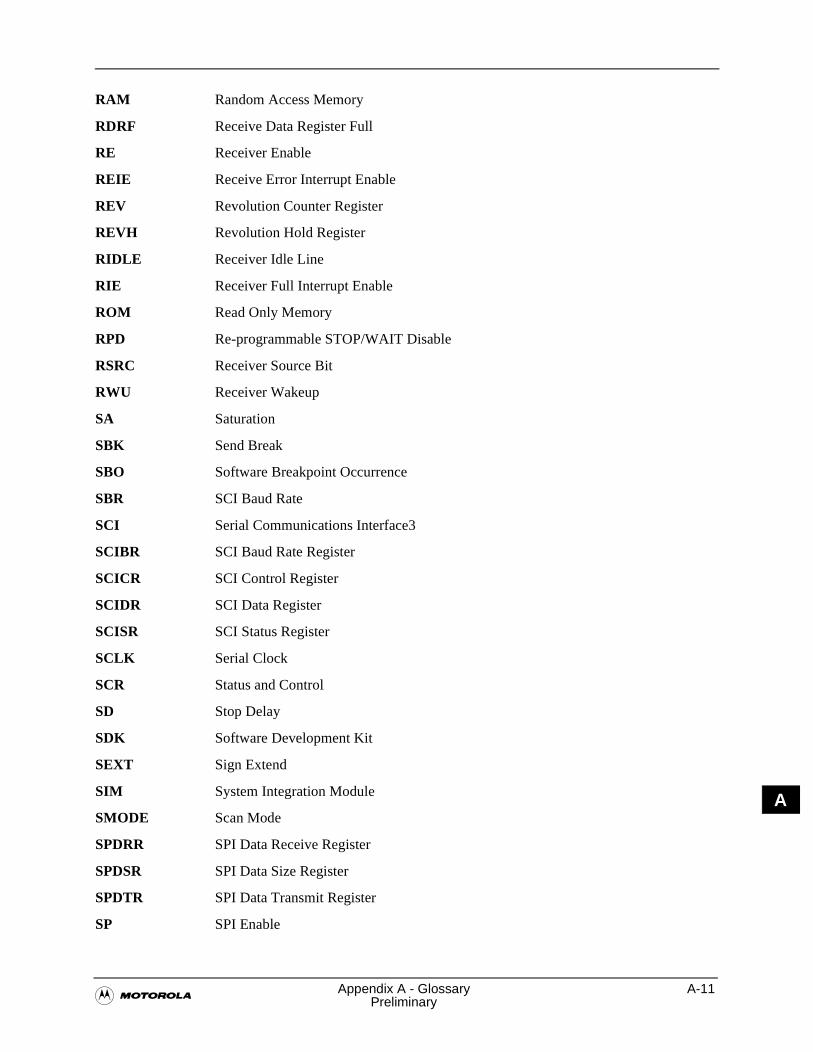
�Appendix A - Glossary A-11
Preliminary
A
RAM Random Access Memory
RDRF Receive Data Register Full
RE Receiver Enable
REIE Receive Error Interrupt Enable
REV Revolution Counter Register
REVH Revolution Hold Register
RIDLE Receiver Idle Line
RIE Receiver Full Interrupt Enable
ROM Read Only Memory
RPD Re-programmable STOP/WAIT Disable
RSRC Receiver Source Bit
RWU Receiver Wakeup
SA Saturation
SBK Send Break
SBO Software Breakpoint Occurrence
SBR SCI Baud Rate
SCI Serial Communications Interface3
SCIBR SCI Baud Rate Register
SCICR SCI Control Register
SCIDR SCI Data Register
SCISR SCI Status Register
SCLK Serial Clock
SCR Status and Control
SD Stop Delay
SDK Software Development Kit
SEXT Sign Extend
SIM System Integration Module
SMODE Scan Mode
SPDRR SPI Data Receive Register
SPDSR SPI Data Size Register
SPDTR SPI Data Transmit Register
SP SPI Enable
A-12 DSP58603/05 User’s Manual�Preliminary
A
SPI Serial Peripheral Interface
SPMSTR SPI Master
SPRF SPI Receiver Full
SPRIE SPI Receiver Interrupt Enable
SPSCR SPI Status Control Register
SPTE SPI Transmitter Empty
SPTIE SPI Transmit Interrupt Enable
SR Status Register
SRM Switched Reluctance Motor
SS Slave Select
SSI Synchronous Serial Interface
SWAI Stop in Wait Mode
SYS_CNTL System Control Register
SYS_STS System Status Register
TAP Test Access Port
TCSR Text Control and Status Register
TCE Test Counter Enable
TCF Timer Compare Flag
TCFIE Timer Compare Flag Interrupt Enable
TDRE Transmit Date Register Empty
TE Transmitter Enable
TEIE Transmitter Empty Interrupt Enable
TEN Test Mode Enable
TERASEL Terase Limit
TESTR Test Register
TFDBK Test Feedback Clock
TFREF Test Reference Frequency Clock
TIDLE Transmitter Idle
TIIE Transmitter Idle Interrupt Enable
TIRQ Test Interrupt Request Register
TISR Test Interrupt Source Register
TM Test Mode bit
�Appendix A - Glossary A-13
Preliminary
A
TMEL Time Limit
TMODE Test Mode bit
TMR Quadrature Timer
TMR PD Timer I/O Pull-up Disable
TNVHL TNVH Limit
TNVSL TNVS Limit
TO Trace Occurrence
TOF Timer Overflow Flag
TOFIE Timer Oerflow Flag Interrupt Enable
TOPNEG Top-side PWM Polarity Bit
TPROGL Tprog Limit
TPGSL TPGS Limit
TRCVL TRCV Limit
TSTREG Test Register
UIR Upper Initialization Register
UPOS Upper Position Hold Register
UPOSH Upper Position Hold Register
VDD Power
VDDA Analog Power
VEL Velocity Counter Register
VELH Velocity Hold Register
VLMODE Value Register Load Mode
VREF Voltage Reference
VRM Variable Reluctance Motor
VSS Ground
VSSA Analog Ground
WAKE Wakeup Condition
WDE Watchdog Enable
WP Write Protect
WSPM Wait State P Memory
WSX Wait State Data Memory
WTR Watchdog Timeout Register
A-14 DSP58603/05 User’s Manual�Preliminary
A
WWW World Wide Web
XDB2 X Data Bus
XE X Address Enable
XIE Index Pulse Interrupt Enable
XIRQ Index Pulse Interrupt Request
XNE Use Negative Edge of Index Pulse
XRAM Data RAM
YE Y Address Enable
ZCI Zero Crossing Interrupt
ZCIE Zero Crossing Interrupt Enable
ZCS Zero Crossing Status
ZSRC Zclock Source
�Appendix B - BSDL Listing B-1
Preliminary
B
Appendix BBSDL Listing

B-2 DSP56F801/803/805/807 User’s Manual�Preliminary
B
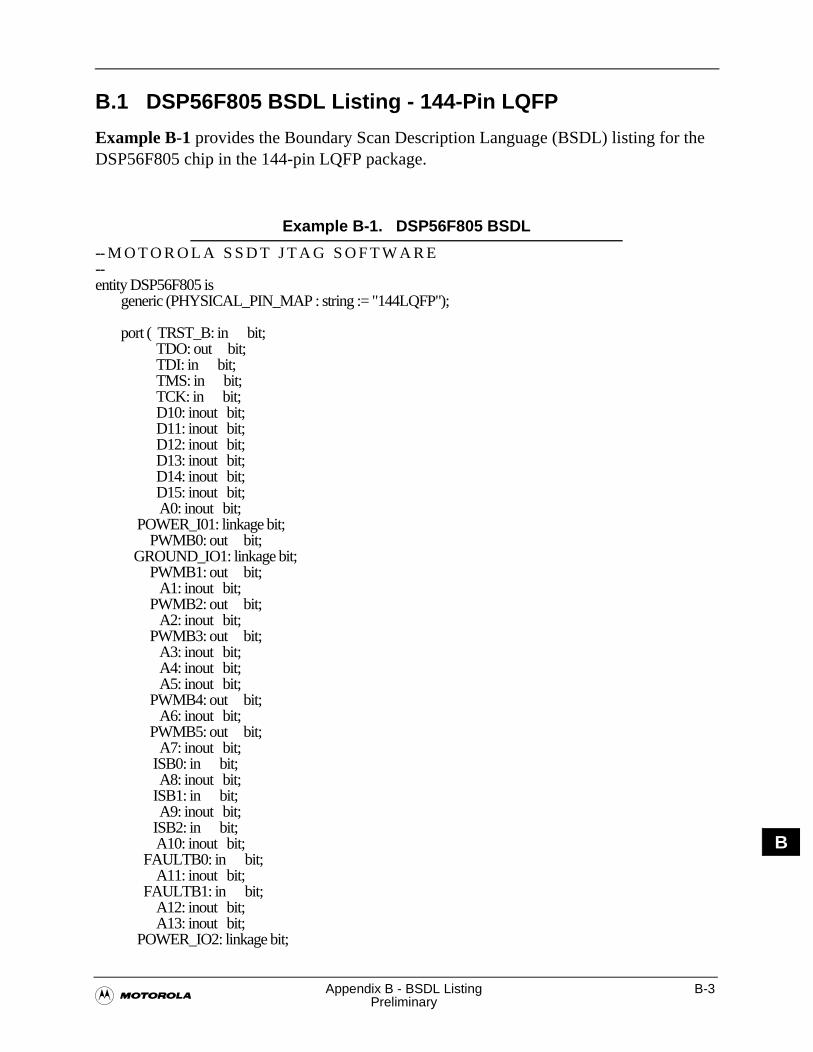
�Appendix B - BSDL Listing B-3
Preliminary
B
B.1 DSP56F805 BSDL Listing - 144-Pin LQFP
Example B-1 provides the Boundary Scan Description Language (BSDL) listing for the DSP56F805 chip in the 144-pin LQFP package.
Example B-1. DSP56F805 BSDL
-- M O T O R O L A S S D T J T A G S O F T W A R E--entity DSP56F805 is generic (PHYSICAL_PIN_MAP : string := "144LQFP");
port ( TRST_B: in bit; TDO: out bit; TDI: in bit; TMS: in bit; TCK: in bit; D10: inout bit; D11: inout bit; D12: inout bit; D13: inout bit; D14: inout bit; D15: inout bit; A0: inout bit; POWER_I01: linkage bit; PWMB0: out bit; GROUND_IO1: linkage bit; PWMB1: out bit; A1: inout bit; PWMB2: out bit; A2: inout bit; PWMB3: out bit; A3: inout bit; A4: inout bit; A5: inout bit; PWMB4: out bit; A6: inout bit; PWMB5: out bit; A7: inout bit; ISB0: in bit; A8: inout bit; ISB1: in bit; A9: inout bit; ISB2: in bit; A10: inout bit; FAULTB0: in bit; A11: inout bit; FAULTB1: in bit; A12: inout bit; A13: inout bit; POWER_IO2: linkage bit;
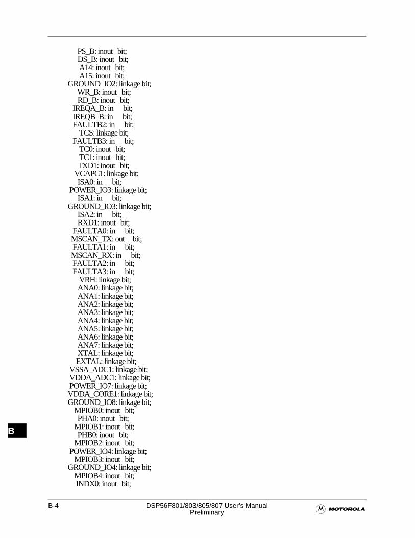
B-4 DSP56F801/803/805/807 User’s Manual�Preliminary
B
PS_B: inout bit; DS_B: inout bit; A14: inout bit; A15: inout bit; GROUND_IO2: linkage bit; WR_B: inout bit; RD_B: inout bit; IREQA_B: in bit; IREQB_B: in bit; FAULTB2: in bit; TCS: linkage bit; FAULTB3: in bit; TC0: inout bit; TC1: inout bit; TXD1: inout bit; VCAPC1: linkage bit; ISA0: in bit; POWER_IO3: linkage bit; ISA1: in bit; GROUND_IO3: linkage bit; ISA2: in bit; RXD1: inout bit; FAULTA0: in bit; MSCAN_TX: out bit; FAULTA1: in bit; MSCAN_RX: in bit; FAULTA2: in bit; FAULTA3: in bit; VRH: linkage bit; ANA0: linkage bit; ANA1: linkage bit; ANA2: linkage bit; ANA3: linkage bit; ANA4: linkage bit; ANA5: linkage bit; ANA6: linkage bit; ANA7: linkage bit; XTAL: linkage bit; EXTAL: linkage bit; VSSA_ADC1: linkage bit; VDDA_ADC1: linkage bit; POWER_IO7: linkage bit; VDDA_CORE1: linkage bit; GROUND_IO8: linkage bit; MPIOB0: inout bit; PHA0: inout bit; MPIOB1: inout bit; PHB0: inout bit; MPIOB2: inout bit; POWER_IO4: linkage bit; MPIOB3: inout bit; GROUND_IO4: linkage bit; MPIOB4: inout bit; INDX0: inout bit;
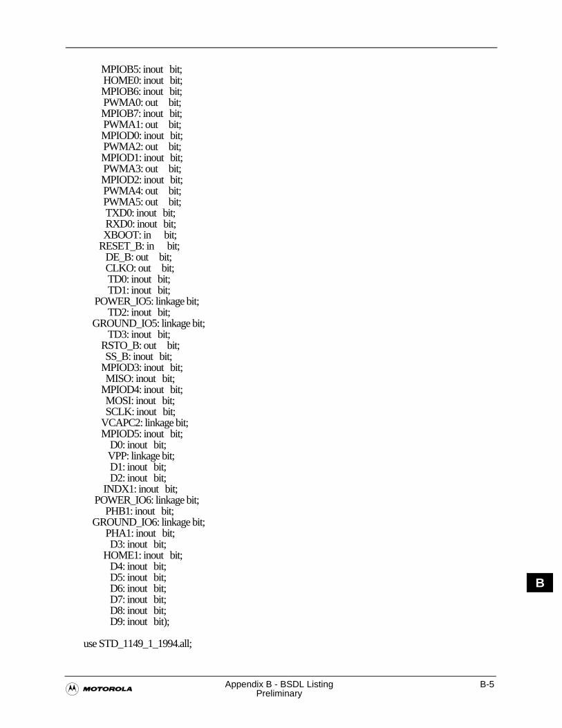
�Appendix B - BSDL Listing B-5
Preliminary
B
MPIOB5: inout bit; HOME0: inout bit; MPIOB6: inout bit; PWMA0: out bit; MPIOB7: inout bit; PWMA1: out bit; MPIOD0: inout bit; PWMA2: out bit; MPIOD1: inout bit; PWMA3: out bit; MPIOD2: inout bit; PWMA4: out bit; PWMA5: out bit; TXD0: inout bit; RXD0: inout bit; XBOOT: in bit; RESET_B: in bit; DE_B: out bit; CLKO: out bit; TD0: inout bit; TD1: inout bit; POWER_IO5: linkage bit; TD2: inout bit; GROUND_IO5: linkage bit; TD3: inout bit; RSTO_B: out bit; SS_B: inout bit; MPIOD3: inout bit; MISO: inout bit; MPIOD4: inout bit; MOSI: inout bit; SCLK: inout bit; VCAPC2: linkage bit; MPIOD5: inout bit; D0: inout bit; VPP: linkage bit; D1: inout bit; D2: inout bit; INDX1: inout bit; POWER_IO6: linkage bit; PHB1: inout bit; GROUND_IO6: linkage bit; PHA1: inout bit; D3: inout bit; HOME1: inout bit; D4: inout bit; D5: inout bit; D6: inout bit; D7: inout bit; D8: inout bit; D9: inout bit);
use STD_1149_1_1994.all;
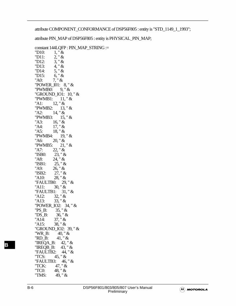
B-6 DSP56F801/803/805/807 User’s Manual�Preliminary
B
attribute COMPONENT_CONFORMANCE of DSP56F805 : entity is "STD_1149_1_1993";
attribute PIN_MAP of DSP56F805 : entity is PHYSICAL_PIN_MAP;
constant 144LQFP : PIN_MAP_STRING := "D10: 1, " & "D11: 2, " & "D12: 3, " & "D13: 4, " & "D14: 5, " & "D15: 6, " & "A0: 7, " & "POWER_I01: 8, " & "PWMB0: 9, " & "GROUND_IO1: 10, " & "PWMB1: 11, " & "A1: 12, " & "PWMB2: 13, " & "A2: 14, " & "PWMB3: 15, " & "A3: 16, " & "A4: 17, " & "A5: 18, " & "PWMB4: 19, " & "A6: 20, " & "PWMB5: 21, " & "A7: 22, " & "ISB0: 23, " & "A8: 24, " & "ISB1: 25, " & "A9: 26, " & "ISB2: 27, " & "A10: 28, " & "FAULTB0: 29, " & "A11: 30, " & "FAULTB1: 31, " & "A12: 32, " & "A13: 33, " & "POWER_IO2: 34, " & "PS_B: 35, " & "DS_B: 36, " & "A14: 37, " & "A15: 38, " & "GROUND_IO2: 39, " & "WR_B: 40, " & "RD_B: 41, " & "IREQA_B: 42, " & "IREQB_B: 43, " & "FAULTB2: 44, " & "TCS: 45, " & "FAULTB3: 46, " & "TCK: 47, " & "TC0: 48, " & "TMS: 49, " &
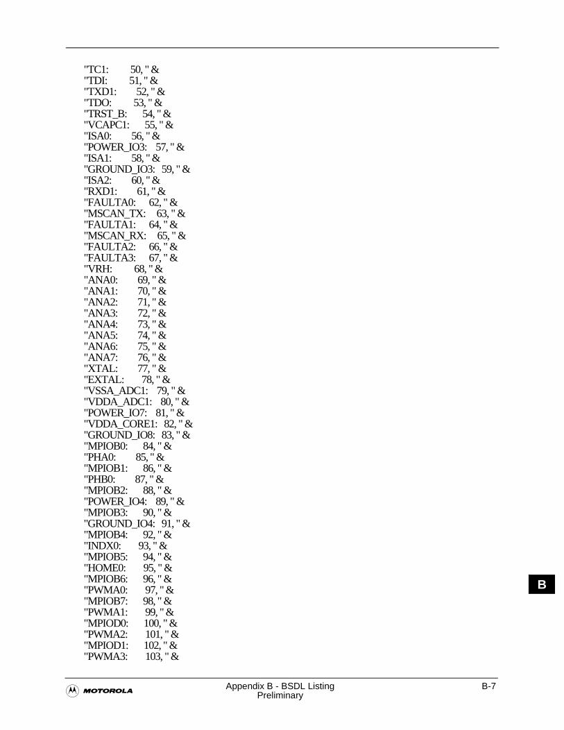
�Appendix B - BSDL Listing B-7
Preliminary
B
"TC1: 50, " & "TDI: 51, " & "TXD1: 52, " & "TDO: 53, " & "TRST_B: 54, " & "VCAPC1: 55, " & "ISA0: 56, " & "POWER_IO3: 57, " & "ISA1: 58, " & "GROUND_IO3: 59, " & "ISA2: 60, " & "RXD1: 61, " & "FAULTA0: 62, " & "MSCAN_TX: 63, " & "FAULTA1: 64, " & "MSCAN_RX: 65, " & "FAULTA2: 66, " & "FAULTA3: 67, " & "VRH: 68, " & "ANA0: 69, " & "ANA1: 70, " & "ANA2: 71, " & "ANA3: 72, " & "ANA4: 73, " & "ANA5: 74, " & "ANA6: 75, " & "ANA7: 76, " & "XTAL: 77, " & "EXTAL: 78, " & "VSSA_ADC1: 79, " & "VDDA_ADC1: 80, " & "POWER_IO7: 81, " & "VDDA_CORE1: 82, " & "GROUND_IO8: 83, " & "MPIOB0: 84, " & "PHA0: 85, " & "MPIOB1: 86, " & "PHB0: 87, " & "MPIOB2: 88, " & "POWER_IO4: 89, " & "MPIOB3: 90, " & "GROUND_IO4: 91, " & "MPIOB4: 92, " & "INDX0: 93, " & "MPIOB5: 94, " & "HOME0: 95, " & "MPIOB6: 96, " & "PWMA0: 97, " & "MPIOB7: 98, " & "PWMA1: 99, " & "MPIOD0: 100, " & "PWMA2: 101, " & "MPIOD1: 102, " & "PWMA3: 103, " &
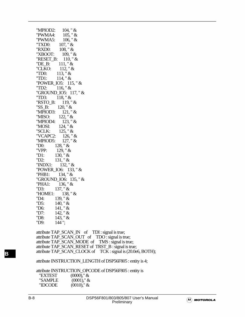
B-8 DSP56F801/803/805/807 User’s Manual�Preliminary
B
"MPIOD2: 104, " & "PWMA4: 105, " & "PWMA5: 106, " & "TXD0: 107, " & "RXD0: 108, " & "XBOOT: 109, " & "RESET_B: 110, " & "DE_B: 111, " & "CLKO: 112, " & "TD0: 113, " & "TD1: 114, " & "POWER_IO5: 115, " & "TD2: 116, " & "GROUND_IO5: 117, " & "TD3: 118, " & "RSTO_B: 119, " & "SS_B: 120, " & "MPIOD3: 121, " & "MISO: 122, " & "MPIOD4: 123, " & "MOSI: 124, " & "SCLK: 125, " & "VCAPC2: 126, " & "MPIOD5: 127, " & "D0: 128, " & "VPP: 129, " & "D1: 130, " & "D2: 131, " & "INDX1: 132, " & "POWER_IO6: 133, " & "PHB1: 134, " & "GROUND_IO6: 135, " & "PHA1: 136, " & "D3: 137, " & "HOME1: 138, " & "D4: 139, " & "D5: 140, " & "D6: 141, " & "D7: 142, " & "D8: 143, " & "D9: 144 ";
attribute TAP_SCAN_IN of TDI : signal is true; attribute TAP_SCAN_OUT of TDO : signal is true; attribute TAP_SCAN_MODE of TMS : signal is true; attribute TAP_SCAN_RESET of TRST_B : signal is true; attribute TAP_SCAN_CLOCK of TCK : signal is (20.0e6, BOTH);
attribute INSTRUCTION_LENGTH of DSP56F805 : entity is 4;
attribute INSTRUCTION_OPCODE of DSP56F805 : entity is "EXTEST (0000)," & "SAMPLE (0001)," & "IDCODE (0010)," &
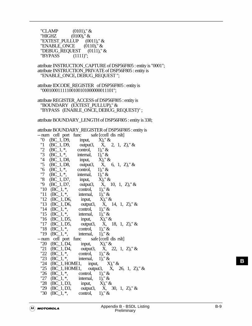
�Appendix B - BSDL Listing B-9
Preliminary
B
"CLAMP (0101)," & "HIGHZ (0100)," & "EXTEST_PULLUP (0011)," & "ENABLE_ONCE (0110)," & "DEBUG_REQUEST (0111)," & "BYPASS (1111)";
attribute INSTRUCTION_CAPTURE of DSP56F805 : entity is "0001"; attribute INSTRUCTION_PRIVATE of DSP56F805 : entity is "ENABLE_ONCE, DEBUG_REQUEST ";
attribute IDCODE_REGISTER of DSP56F805 : entity is "00010001111100100101000000011101";
attribute REGISTER_ACCESS of DSP56F805 : entity is "BOUNDARY (EXTEST_PULLUP)," & "BYPASS (ENABLE_ONCE, DEBUG_REQUEST)" ;
attribute BOUNDARY_LENGTH of DSP56F805 : entity is 338;
attribute BOUNDARY_REGISTER of DSP56F805 : entity is -- num cell port func safe [ccell dis rslt] "0 (BC_1, D9, input, X)," & "1 (BC_1, D9, output3, X, 2, 1, Z)," & "2 (BC_1, *, control, 1)," & "3 (BC_1, *, internal, 1)," & "4 (BC_1, D8, input, X)," & "5 (BC_1, D8, output3, X, 6, 1, Z)," & "6 (BC_1, *, control, 1)," & "7 (BC_1, *, internal, 1)," & "8 (BC_1, D7, input, X)," & "9 (BC_1, D7, output3, X, 10, 1, Z)," & "10 (BC_1, *, control, 1)," & "11 (BC_1, *, internal, 1)," & "12 (BC_1, D6, input, X)," & "13 (BC_1, D6, output3, X, 14, 1, Z)," & "14 (BC_1, *, control, 1)," & "15 (BC_1, *, internal, 1)," & "16 (BC_1, D5, input, X)," & "17 (BC_1, D5, output3, X, 18, 1, Z)," & "18 (BC_1, *, control, 1)," & "19 (BC_1, *, internal, 1)," & -- num cell port func safe [ccell dis rslt] "20 (BC_1, D4, input, X)," & "21 (BC_1, D4, output3, X, 22, 1, Z)," & "22 (BC_1, *, control, 1)," & "23 (BC_1, *, internal, 1)," & "24 (BC_1, HOME1, input, X)," & "25 (BC_1, HOME1, output3, X, 26, 1, Z)," & "26 (BC_1, *, control, 1)," & "27 (BC_1, *, internal, 1)," & "28 (BC_1, D3, input, X)," & "29 (BC_1, D3, output3, X, 30, 1, Z)," & "30 (BC_1, *, control, 1)," &
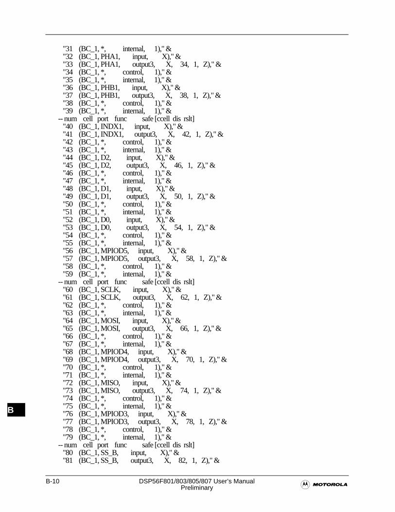
B-10 DSP56F801/803/805/807 User’s Manual�Preliminary
B
"31 (BC_1, *, internal, 1)," & "32 (BC_1, PHA1, input, X)," & "33 (BC_1, PHA1, output3, X, 34, 1, Z)," & "34 (BC_1, *, control, 1)," & "35 (BC_1, *, internal, 1)," & "36 (BC_1, PHB1, input, X)," & "37 (BC_1, PHB1, output3, X, 38, 1, Z)," & "38 (BC_1, *, control, 1)," & "39 (BC_1, *, internal, 1)," & -- num cell port func safe [ccell dis rslt] "40 (BC_1, INDX1, input, X)," & "41 (BC_1, INDX1, output3, X, 42, 1, Z)," & "42 (BC_1, *, control, 1)," & "43 (BC_1, *, internal, 1)," & "44 (BC_1, D2, input, X)," & "45 (BC_1, D2, output3, X, 46, 1, Z)," & "46 (BC_1, *, control, 1)," & "47 (BC_1, *, internal, 1)," & "48 (BC_1, D1, input, X)," & "49 (BC_1, D1, output3, X, 50, 1, Z)," & "50 (BC_1, *, control, 1)," & "51 (BC_1, *, internal, 1)," & "52 (BC_1, D0, input, X)," & "53 (BC_1, D0, output3, X, 54, 1, Z)," & "54 (BC_1, *, control, 1)," & "55 (BC_1, *, internal, 1)," & "56 (BC_1, MPIOD5, input, X)," & "57 (BC_1, MPIOD5, output3, X, 58, 1, Z)," & "58 (BC_1, *, control, 1)," & "59 (BC_1, *, internal, 1)," & -- num cell port func safe [ccell dis rslt] "60 (BC_1, SCLK, input, X)," & "61 (BC_1, SCLK, output3, X, 62, 1, Z)," & "62 (BC_1, *, control, 1)," & "63 (BC_1, *, internal, 1)," & "64 (BC_1, MOSI, input, X)," & "65 (BC_1, MOSI, output3, X, 66, 1, Z)," & "66 (BC_1, *, control, 1)," & "67 (BC_1, *, internal, 1)," & "68 (BC_1, MPIOD4, input, X)," & "69 (BC_1, MPIOD4, output3, X, 70, 1, Z)," & "70 (BC_1, *, control, 1)," & "71 (BC_1, *, internal, 1)," & "72 (BC_1, MISO, input, X)," & "73 (BC_1, MISO, output3, X, 74, 1, Z)," & "74 (BC_1, *, control, 1)," & "75 (BC_1, *, internal, 1)," & "76 (BC_1, MPIOD3, input, X)," & "77 (BC_1, MPIOD3, output3, X, 78, 1, Z)," & "78 (BC_1, *, control, 1)," & "79 (BC_1, *, internal, 1)," & -- num cell port func safe [ccell dis rslt] "80 (BC_1, SS_B, input, X)," & "81 (BC_1, SS_B, output3, X, 82, 1, Z)," &
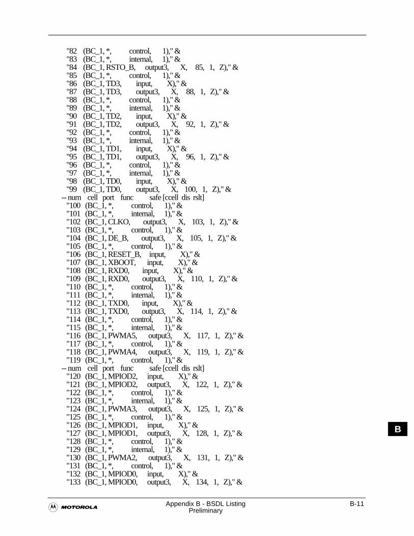
�Appendix B - BSDL Listing B-11
Preliminary
B
"82 (BC_1, *, control, 1)," & "83 (BC_1, *, internal, 1)," & "84 (BC_1, RSTO_B, output3, X, 85, 1, Z)," & "85 (BC_1, *, control, 1)," & "86 (BC_1, TD3, input, X)," & "87 (BC_1, TD3, output3, X, 88, 1, Z)," & "88 (BC_1, *, control, 1)," & "89 (BC_1, *, internal, 1)," & "90 (BC_1, TD2, input, X)," & "91 (BC_1, TD2, output3, X, 92, 1, Z)," & "92 (BC_1, *, control, 1)," & "93 (BC_1, *, internal, 1)," & "94 (BC_1, TD1, input, X)," & "95 (BC_1, TD1, output3, X, 96, 1, Z)," & "96 (BC_1, *, control, 1)," & "97 (BC_1, *, internal, 1)," & "98 (BC_1, TD0, input, X)," & "99 (BC_1, TD0, output3, X, 100, 1, Z)," & -- num cell port func safe [ccell dis rslt] "100 (BC_1, *, control, 1)," & "101 (BC_1, *, internal, 1)," & "102 (BC_1, CLKO, output3, X, 103, 1, Z)," & "103 (BC_1, *, control, 1)," & "104 (BC_1, DE_B, output3, X, 105, 1, Z)," & "105 (BC_1, *, control, 1)," & "106 (BC_1, RESET_B, input, X)," & "107 (BC_1, XBOOT, input, X)," & "108 (BC_1, RXD0, input, X)," & "109 (BC_1, RXD0, output3, X, 110, 1, Z)," & "110 (BC_1, *, control, 1)," & "111 (BC_1, *, internal, 1)," & "112 (BC_1, TXD0, input, X)," & "113 (BC_1, TXD0, output3, X, 114, 1, Z)," & "114 (BC_1, *, control, 1)," & "115 (BC_1, *, internal, 1)," & "116 (BC_1, PWMA5, output3, X, 117, 1, Z)," & "117 (BC_1, *, control, 1)," & "118 (BC_1, PWMA4, output3, X, 119, 1, Z)," & "119 (BC_1, *, control, 1)," & -- num cell port func safe [ccell dis rslt] "120 (BC_1, MPIOD2, input, X)," & "121 (BC_1, MPIOD2, output3, X, 122, 1, Z)," & "122 (BC_1, *, control, 1)," & "123 (BC_1, *, internal, 1)," & "124 (BC_1, PWMA3, output3, X, 125, 1, Z)," & "125 (BC_1, *, control, 1)," & "126 (BC_1, MPIOD1, input, X)," & "127 (BC_1, MPIOD1, output3, X, 128, 1, Z)," & "128 (BC_1, *, control, 1)," & "129 (BC_1, *, internal, 1)," & "130 (BC_1, PWMA2, output3, X, 131, 1, Z)," & "131 (BC_1, *, control, 1)," & "132 (BC_1, MPIOD0, input, X)," & "133 (BC_1, MPIOD0, output3, X, 134, 1, Z)," &
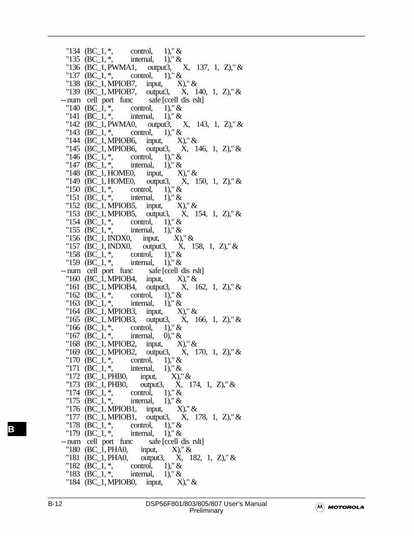
B-12 DSP56F801/803/805/807 User’s Manual�Preliminary
B
"134 (BC_1, *, control, 1)," & "135 (BC_1, *, internal, 1)," & "136 (BC_1, PWMA1, output3, X, 137, 1, Z)," & "137 (BC_1, *, control, 1)," & "138 (BC_1, MPIOB7, input, X)," & "139 (BC_1, MPIOB7, output3, X, 140, 1, Z)," & -- num cell port func safe [ccell dis rslt] "140 (BC_1, *, control, 1)," & "141 (BC_1, *, internal, 1)," & "142 (BC_1, PWMA0, output3, X, 143, 1, Z)," & "143 (BC_1, *, control, 1)," & "144 (BC_1, MPIOB6, input, X)," & "145 (BC_1, MPIOB6, output3, X, 146, 1, Z)," & "146 (BC_1, *, control, 1)," & "147 (BC_1, *, internal, 1)," & "148 (BC_1, HOME0, input, X)," & "149 (BC_1, HOME0, output3, X, 150, 1, Z)," & "150 (BC_1, *, control, 1)," & "151 (BC_1, *, internal, 1)," & "152 (BC_1, MPIOB5, input, X)," & "153 (BC_1, MPIOB5, output3, X, 154, 1, Z)," & "154 (BC_1, *, control, 1)," & "155 (BC_1, *, internal, 1)," & "156 (BC_1, INDX0, input, X)," & "157 (BC_1, INDX0, output3, X, 158, 1, Z)," & "158 (BC_1, *, control, 1)," & "159 (BC_1, *, internal, 1)," & -- num cell port func safe [ccell dis rslt] "160 (BC_1, MPIOB4, input, X)," & "161 (BC_1, MPIOB4, output3, X, 162, 1, Z)," & "162 (BC_1, *, control, 1)," & "163 (BC_1, *, internal, 1)," & "164 (BC_1, MPIOB3, input, X)," & "165 (BC_1, MPIOB3, output3, X, 166, 1, Z)," & "166 (BC_1, *, control, 1)," & "167 (BC_1, *, internal, 0)," & "168 (BC_1, MPIOB2, input, X)," & "169 (BC_1, MPIOB2, output3, X, 170, 1, Z)," & "170 (BC_1, *, control, 1)," & "171 (BC_1, *, internal, 1)," & "172 (BC_1, PHB0, input, X)," & "173 (BC_1, PHB0, output3, X, 174, 1, Z)," & "174 (BC_1, *, control, 1)," & "175 (BC_1, *, internal, 1)," & "176 (BC_1, MPIOB1, input, X)," & "177 (BC_1, MPIOB1, output3, X, 178, 1, Z)," & "178 (BC_1, *, control, 1)," & "179 (BC_1, *, internal, 1)," & -- num cell port func safe [ccell dis rslt] "180 (BC_1, PHA0, input, X)," & "181 (BC_1, PHA0, output3, X, 182, 1, Z)," & "182 (BC_1, *, control, 1)," & "183 (BC_1, *, internal, 1)," & "184 (BC_1, MPIOB0, input, X)," &
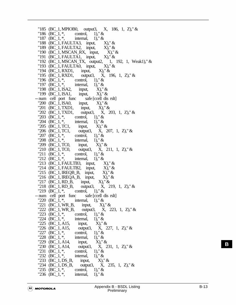
�Appendix B - BSDL Listing B-13
Preliminary
B
"185 (BC_1, MPIOB0, output3, X, 186, 1, Z)," & "186 (BC_1, *, control, 1)," & "187 (BC_1, *, internal, 1)," & "188 (BC_1, FAULTA3, input, X)," & "189 (BC_1, FAULTA2, input, X)," & "190 (BC_1, MSCAN_RX, input, X)," & "191 (BC_1, FAULTA1, input, X)," & "192 (BC_1, MSCAN_TX, output2, 1, 192, 1, Weak1)," & "193 (BC_1, FAULTA0, input, X)," & "194 (BC_1, RXD1, input, X)," & "195 (BC_1, RXD1, output3, X, 196, 1, Z)," & "196 (BC_1, *, control, 1)," & "197 (BC_1, *, internal, 1)," & "198 (BC_1, ISA2, input, X)," & "199 (BC_1, ISA1, input, X)," & -- num cell port func safe [ccell dis rslt] "200 (BC_1, ISA0, input, X)," & "201 (BC_1, TXD1, input, X)," & "202 (BC_1, TXD1, output3, X, 203, 1, Z)," & "203 (BC_1, *, control, 1)," & "204 (BC_1, *, internal, 1)," & "205 (BC_1, TC1, input, X)," & "206 (BC_1, TC1, output3, X, 207, 1, Z)," & "207 (BC_1, *, control, 1)," & "208 (BC_1, *, internal, 1)," & "209 (BC_1, TC0, input, X)," & "210 (BC_1, TC0, output3, X, 211, 1, Z)," & "211 (BC_1, *, control, 1)," & "212 (BC_1, *, internal, 1)," & "213 (BC_1, FAULTB3, input, X)," & "214 (BC_1, FAULTB2, input, X)," & "215 (BC_1, IREQB_B, input, X)," & "216 (BC_1, IREQA_B, input, X)," & "217 (BC_1, RD_B, input, X)," & "218 (BC_1, RD_B, output3, X, 219, 1, Z)," & "219 (BC_1, *, control, 1)," & -- num cell port func safe [ccell dis rslt] "220 (BC_1, *, internal, 1)," & "221 (BC_1, WR_B, input, X)," & "222 (BC_1, WR_B, output3, X, 223, 1, Z)," & "223 (BC_1, *, control, 1)," & "224 (BC_1, *, internal, 1)," & "225 (BC_1, A15, input, X)," & "226 (BC_1, A15, output3, X, 227, 1, Z)," & "227 (BC_1, *, control, 1)," & "228 (BC_1, *, internal, 1)," & "229 (BC_1, A14, input, X)," & "230 (BC_1, A14, output3, X, 231, 1, Z)," & "231 (BC_1, *, control, 1)," & "232 (BC_1, *, internal, 1)," & "233 (BC_1, DS_B, input, X)," & "234 (BC_1, DS_B, output3, X, 235, 1, Z)," & "235 (BC_1, *, control, 1)," & "236 (BC_1, *, internal, 1)," &
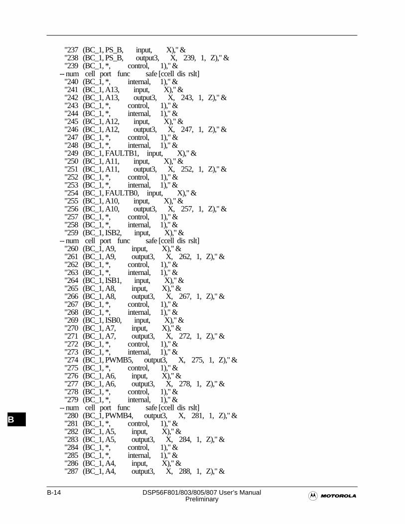
B-14 DSP56F801/803/805/807 User’s Manual�Preliminary
B
"237 (BC_1, PS_B, input, X)," & "238 (BC_1, PS_B, output3, X, 239, 1, Z)," & "239 (BC_1, *, control, 1)," & -- num cell port func safe [ccell dis rslt] "240 (BC_1, *, internal, 1)," & "241 (BC_1, A13, input, X)," & "242 (BC_1, A13, output3, X, 243, 1, Z)," & "243 (BC_1, *, control, 1)," & "244 (BC_1, *, internal, 1)," & "245 (BC_1, A12, input, X)," & "246 (BC_1, A12, output3, X, 247, 1, Z)," & "247 (BC_1, *, control, 1)," & "248 (BC_1, *, internal, 1)," & "249 (BC_1, FAULTB1, input, X)," & "250 (BC_1, A11, input, X)," & "251 (BC_1, A11, output3, X, 252, 1, Z)," & "252 (BC_1, *, control, 1)," & "253 (BC_1, *, internal, 1)," & "254 (BC_1, FAULTB0, input, X)," & "255 (BC_1, A10, input, X)," & "256 (BC_1, A10, output3, X, 257, 1, Z)," & "257 (BC_1, *, control, 1)," & "258 (BC_1, *, internal, 1)," & "259 (BC_1, ISB2, input, X)," & -- num cell port func safe [ccell dis rslt] "260 (BC_1, A9, input, X)," & "261 (BC_1, A9, output3, X, 262, 1, Z)," & "262 (BC_1, *, control, 1)," & "263 (BC_1, *, internal, 1)," & "264 (BC_1, ISB1, input, X)," & "265 (BC_1, A8, input, X)," & "266 (BC_1, A8, output3, X, 267, 1, Z)," & "267 (BC_1, *, control, 1)," & "268 (BC_1, *, internal, 1)," & "269 (BC_1, ISB0, input, X)," & "270 (BC_1, A7, input, X)," & "271 (BC_1, A7, output3, X, 272, 1, Z)," & "272 (BC_1, *, control, 1)," & "273 (BC_1, *, internal, 1)," & "274 (BC_1, PWMB5, output3, X, 275, 1, Z)," & "275 (BC_1, *, control, 1)," & "276 (BC_1, A6, input, X)," & "277 (BC_1, A6, output3, X, 278, 1, Z)," & "278 (BC_1, *, control, 1)," & "279 (BC_1, *, internal, 1)," & -- num cell port func safe [ccell dis rslt] "280 (BC_1, PWMB4, output3, X, 281, 1, Z)," & "281 (BC_1, *, control, 1)," & "282 (BC_1, A5, input, X)," & "283 (BC_1, A5, output3, X, 284, 1, Z)," & "284 (BC_1, *, control, 1)," & "285 (BC_1, *, internal, 1)," & "286 (BC_1, A4, input, X)," & "287 (BC_1, A4, output3, X, 288, 1, Z)," &
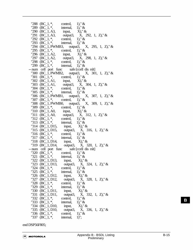
�Appendix B - BSDL Listing B-15
Preliminary
B
"288 (BC_1, *, control, 1)," & "289 (BC_1, *, internal, 1)," & "290 (BC_1, A3, input, X)," & "291 (BC_1, A3, output3, X, 292, 1, Z)," & "292 (BC_1, *, control, 1)," & "293 (BC_1, *, internal, 1)," & "294 (BC_1, PWMB3, output3, X, 295, 1, Z)," & "295 (BC_1, *, control, 1)," & "296 (BC_1, A2, input, X)," & "297 (BC_1, A2, output3, X, 298, 1, Z)," & "298 (BC_1, *, control, 1)," & "299 (BC_1, *, internal, 1)," & -- num cell port func safe [ccell dis rslt] "300 (BC_1, PWMB2, output3, X, 301, 1, Z)," & "301 (BC_1, *, control, 1)," & "302 (BC_1, A1, input, X)," & "303 (BC_1, A1, output3, X, 304, 1, Z)," & "304 (BC_1, *, control, 1)," & "305 (BC_1, *, internal, 1)," & "306 (BC_1, PWMB1, output3, X, 307, 1, Z)," & "307 (BC_1, *, control, 1)," & "308 (BC_1, PWMB0, output3, X, 309, 1, Z)," & "309 (BC_1, *, control, 1)," & "310 (BC_1, A0, input, X)," & "311 (BC_1, A0, output3, X, 312, 1, Z)," & "312 (BC_1, *, control, 1)," & "313 (BC_1, *, internal, 1)," & "314 (BC_1, D15, input, X)," & "315 (BC_1, D15, output3, X, 316, 1, Z)," & "316 (BC_1, *, control, 1)," & "317 (BC_1, *, internal, 1)," & "318 (BC_1, D14, input, X)," & "319 (BC_1, D14, output3, X, 320, 1, Z)," & -- num cell port func safe [ccell dis rslt] "320 (BC_1, *, control, 1)," & "321 (BC_1, *, internal, 1)," & "322 (BC_1, D13, input, X)," & "323 (BC_1, D13, output3, X, 324, 1, Z)," & "324 (BC_1, *, control, 1)," & "325 (BC_1, *, internal, 1)," & "326 (BC_1, D12, input, X)," & "327 (BC_1, D12, output3, X, 328, 1, Z)," & "328 (BC_1, *, control, 1)," & "329 (BC_1, *, internal, 1)," & "330 (BC_1, D11, input, X)," & "331 (BC_1, D11, output3, X, 332, 1, Z)," & "332 (BC_1, *, control, 1)," & "333 (BC_1, *, internal, 1)," & "334 (BC_1, D10, input, X)," & "335 (BC_1, D10, output3, X, 336, 1, Z)," & "336 (BC_1, *, control, 1)," & "337 (BC_1, *, internal, 1)";
end DSP56F805;
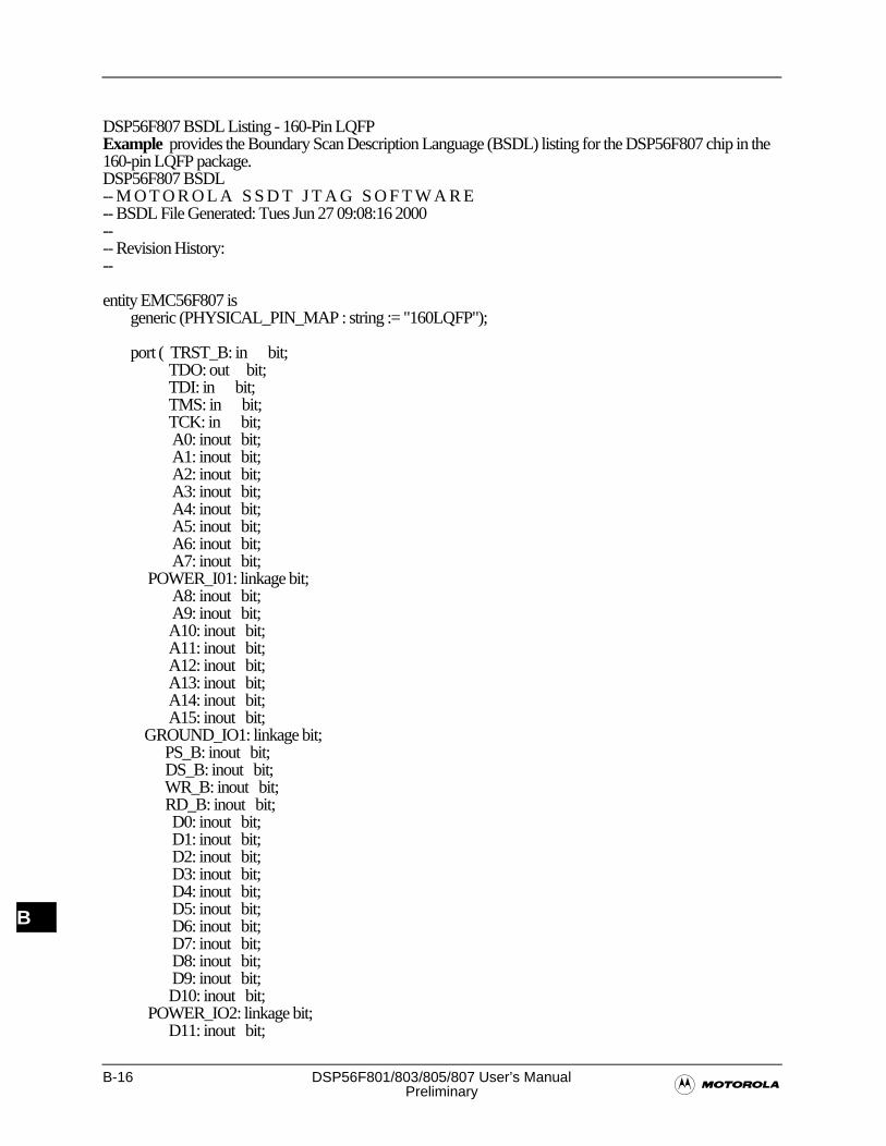
B-16 DSP56F801/803/805/807 User’s Manual�Preliminary
B
DSP56F807 BSDL Listing - 160-Pin LQFPExample provides the Boundary Scan Description Language (BSDL) listing for the DSP56F807 chip in the 160-pin LQFP package.DSP56F807 BSDL-- M O T O R O L A S S D T J T A G S O F T W A R E-- BSDL File Generated: Tues Jun 27 09:08:16 2000---- Revision History:--
entity EMC56F807 is generic (PHYSICAL_PIN_MAP : string := "160LQFP");
port ( TRST_B: in bit; TDO: out bit; TDI: in bit; TMS: in bit; TCK: in bit; A0: inout bit; A1: inout bit; A2: inout bit; A3: inout bit; A4: inout bit; A5: inout bit; A6: inout bit; A7: inout bit; POWER_I01: linkage bit; A8: inout bit; A9: inout bit; A10: inout bit; A11: inout bit; A12: inout bit; A13: inout bit; A14: inout bit; A15: inout bit; GROUND_IO1: linkage bit; PS_B: inout bit; DS_B: inout bit; WR_B: inout bit; RD_B: inout bit; D0: inout bit; D1: inout bit; D2: inout bit; D3: inout bit; D4: inout bit; D5: inout bit; D6: inout bit; D7: inout bit; D8: inout bit; D9: inout bit; D10: inout bit; POWER_IO2: linkage bit; D11: inout bit;
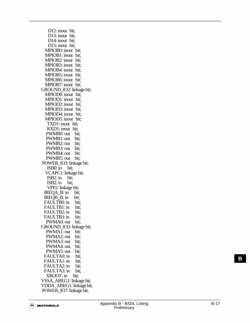
�Appendix B - BSDL Listing B-17
Preliminary
B
D12: inout bit; D13: inout bit; D14: inout bit; D15: inout bit; MPIOB0: inout bit; MPIOB1: inout bit; MPIOB2: inout bit; MPIOB3: inout bit; MPIOB4: inout bit; MPIOB5: inout bit; MPIOB6: inout bit; MPIOB7: inout bit; GROUND_IO2: linkage bit; MPIOD0: inout bit; MPIOD1: inout bit; MPIOD2: inout bit; MPIOD3: inout bit; MPIOD4: inout bit; MPIOD5: inout bit; TXD1: inout bit; RXD1: inout bit; PWMB0: out bit; PWMB1: out bit; PWMB2: out bit; PWMB3: out bit; PWMB4: out bit; PWMB5: out bit; POWER_IO3: linkage bit; ISB0: in bit; VCAPC1: linkage bit; ISB1: in bit; ISB2: in bit; VPP2: linkage bit; IREQA_B: in bit; IREQB_B: in bit; FAULTB0: in bit; FAULTB1: in bit; FAULTB2: in bit; FAULTB3: in bit; PWMA0: out bit; GROUND_IO3: linkage bit; PWMA1: out bit; PWMA2: out bit; PWMA3: out bit; PWMA4: out bit; PWMA5: out bit; FAULTA0: in bit; FAULTA1: in bit; FAULTA2: in bit; FAULTA3: in bit; XBOOT: in bit; VSSA_AREG1: linkage bit; VDDA_AREG1: linkage bit; POWER_IO7: linkage bit;
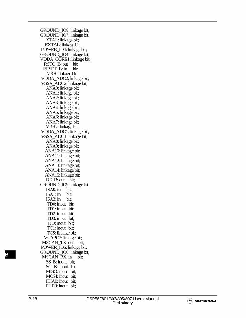
B-18 DSP56F801/803/805/807 User’s Manual�Preliminary
B
GROUND_IO8: linkage bit; GROUND_IO7: linkage bit; XTAL: linkage bit; EXTAL: linkage bit; POWER_IO4: linkage bit; GROUND_IO4: linkage bit; VDDA_CORE1: linkage bit; RSTO_B: out bit; RESET_B: in bit; VRH: linkage bit; VDDA_ADC2: linkage bit; VSSA_ADC2: linkage bit; ANA0: linkage bit; ANA1: linkage bit; ANA2: linkage bit; ANA3: linkage bit; ANA4: linkage bit; ANA5: linkage bit; ANA6: linkage bit; ANA7: linkage bit; VRH2: linkage bit; VDDA_ADC1: linkage bit; VSSA_ADC1: linkage bit; ANA8: linkage bit; ANA9: linkage bit; ANA10: linkage bit; ANA11: linkage bit; ANA12: linkage bit; ANA13: linkage bit; ANA14: linkage bit; ANA15: linkage bit; DE_B: out bit; GROUND_IO9: linkage bit; ISA0: in bit; ISA1: in bit; ISA2: in bit; TD0: inout bit; TD1: inout bit; TD2: inout bit; TD3: inout bit; TC0: inout bit; TC1: inout bit; TCS: linkage bit; VCAPC2: linkage bit; MSCAN_TX: out bit; POWER_IO6: linkage bit; GROUND_IO6: linkage bit; MSCAN_RX: in bit; SS_B: inout bit; SCLK: inout bit; MISO: inout bit; MOSI: inout bit; PHA0: inout bit; PHB0: inout bit;
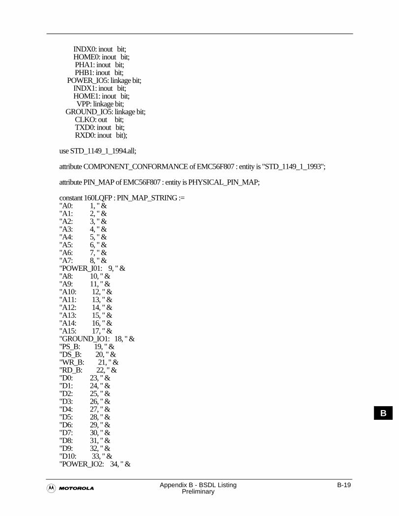
�Appendix B - BSDL Listing B-19
Preliminary
B
INDX0: inout bit; HOME0: inout bit; PHA1: inout bit; PHB1: inout bit; POWER_IO5: linkage bit; INDX1: inout bit; HOME1: inout bit; VPP: linkage bit; GROUND_IO5: linkage bit; CLKO: out bit; TXD0: inout bit; RXD0: inout bit);
use STD_1149_1_1994.all;
attribute COMPONENT_CONFORMANCE of EMC56F807 : entity is "STD_1149_1_1993";
attribute PIN_MAP of EMC56F807 : entity is PHYSICAL_PIN_MAP;
constant 160LQFP : PIN_MAP_STRING := "A0: 1, " & "A1: 2, " & "A2: 3, " & "A3: 4, " & "A4: 5, " & "A5: 6, " & "A6: 7, " & "A7: 8, " & "POWER_I01: 9, " & "A8: 10, " & "A9: 11, " & "A10: 12, " & "A11: 13, " & "A12: 14, " & "A13: 15, " & "A14: 16, " & "A15: 17, " & "GROUND_IO1: 18, " & "PS_B: 19, " & "DS_B: 20, " & "WR_B: 21, " & "RD_B: 22, " & "D0: 23, " & "D1: 24, " & "D2: 25, " & "D3: 26, " & "D4: 27, " & "D5: 28, " & "D6: 29, " & "D7: 30, " & "D8: 31, " & "D9: 32, " & "D10: 33, " & "POWER_IO2: 34, " &
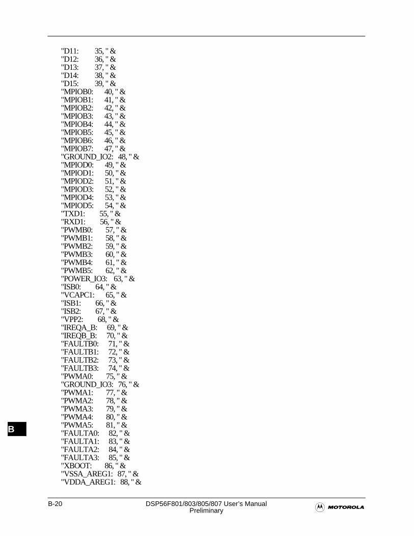
B-20 DSP56F801/803/805/807 User’s Manual�Preliminary
B
"D11: 35, " & "D12: 36, " & "D13: 37, " & "D14: 38, " & "D15: 39, " & "MPIOB0: 40, " & "MPIOB1: 41, " & "MPIOB2: 42, " & "MPIOB3: 43, " & "MPIOB4: 44, " & "MPIOB5: 45, " & "MPIOB6: 46, " & "MPIOB7: 47, " & "GROUND_IO2: 48, " & "MPIOD0: 49, " & "MPIOD1: 50, " & "MPIOD2: 51, " & "MPIOD3: 52, " & "MPIOD4: 53, " & "MPIOD5: 54, " & "TXD1: 55, " & "RXD1: 56, " & "PWMB0: 57, " & "PWMB1: 58, " & "PWMB2: 59, " & "PWMB3: 60, " & "PWMB4: 61, " & "PWMB5: 62, " & "POWER_IO3: 63, " & "ISB0: 64, " & "VCAPC1: 65, " & "ISB1: 66, " & "ISB2: 67, " & "VPP2: 68, " & "IREQA_B: 69, " & "IREQB_B: 70, " & "FAULTB0: 71, " & "FAULTB1: 72, " & "FAULTB2: 73, " & "FAULTB3: 74, " & "PWMA0: 75, " & "GROUND_IO3: 76, " & "PWMA1: 77, " & "PWMA2: 78, " & "PWMA3: 79, " & "PWMA4: 80, " & "PWMA5: 81, " & "FAULTA0: 82, " & "FAULTA1: 83, " & "FAULTA2: 84, " & "FAULTA3: 85, " & "XBOOT: 86, " & "VSSA_AREG1: 87, " & "VDDA_AREG1: 88, " &
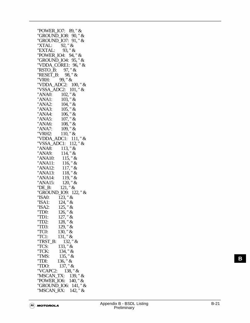
�Appendix B - BSDL Listing B-21
Preliminary
B
"POWER_IO7: 89, " & "GROUND_IO8: 90, " & "GROUND_IO7: 91, " & "XTAL: 92, " & "EXTAL: 93, " & "POWER_IO4: 94, " & "GROUND_IO4: 95, " & "VDDA_CORE1: 96, " & "RSTO_B: 97, " & "RESET_B: 98, " & "VRH: 99, " & "VDDA_ADC2: 100, " & "VSSA_ADC2: 101, " & "ANA0: 102, " & "ANA1: 103, " & "ANA2: 104, " & "ANA3: 105, " & "ANA4: 106, " & "ANA5: 107, " & "ANA6: 108, " & "ANA7: 109, " & "VRH2: 110, " & "VDDA_ADC1: 111, " & "VSSA_ADC1: 112, " & "ANA8: 113, " & "ANA9: 114, " & "ANA10: 115, " & "ANA11: 116, " & "ANA12: 117, " & "ANA13: 118, " & "ANA14: 119, " & "ANA15: 120, " & "DE_B: 121, " & "GROUND_IO9: 122, " & "ISA0: 123, " & "ISA1: 124, " & "ISA2: 125, " & "TD0: 126, " & "TD1: 127, " & "TD2: 128, " & "TD3: 129, " & "TC0: 130, " & "TC1: 131, " & "TRST_B: 132, " & "TCS: 133, " & "TCK: 134, " & "TMS: 135, " & "TDI: 136, " & "TDO: 137, " & "VCAPC2: 138, " & "MSCAN_TX: 139, " & "POWER_IO6: 140, " & "GROUND_IO6: 141, " & "MSCAN_RX: 142, " &
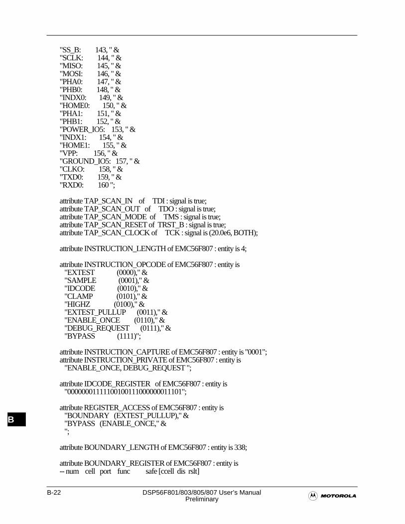
B-22 DSP56F801/803/805/807 User’s Manual�Preliminary
B
"SS_B: 143, " & "SCLK: 144, " & "MISO: 145, " & "MOSI: 146, " & "PHA0: 147, " & "PHB0: 148, " & "INDX0: 149, " & "HOME0: 150, " & "PHA1: 151, " & "PHB1: 152, " & "POWER_IO5: 153, " & "INDX1: 154, " & "HOME1: 155, " & "VPP: 156, " & "GROUND_IO5: 157, " & "CLKO: 158, " & "TXD0: 159, " & "RXD0: 160 ";
attribute TAP_SCAN_IN of TDI : signal is true; attribute TAP_SCAN_OUT of TDO : signal is true; attribute TAP_SCAN_MODE of TMS : signal is true; attribute TAP_SCAN_RESET of TRST_B : signal is true; attribute TAP_SCAN_CLOCK of TCK : signal is (20.0e6, BOTH);
attribute INSTRUCTION_LENGTH of EMC56F807 : entity is 4;
attribute INSTRUCTION_OPCODE of EMC56F807 : entity is "EXTEST (0000)," & "SAMPLE (0001)," & "IDCODE (0010)," & "CLAMP (0101)," & "HIGHZ (0100)," & "EXTEST_PULLUP (0011)," & "ENABLE_ONCE (0110)," & "DEBUG_REQUEST (0111)," & "BYPASS (1111)";
attribute INSTRUCTION_CAPTURE of EMC56F807 : entity is "0001"; attribute INSTRUCTION_PRIVATE of EMC56F807 : entity is "ENABLE_ONCE, DEBUG_REQUEST ";
attribute IDCODE_REGISTER of EMC56F807 : entity is "00000001111100100111000000011101";
attribute REGISTER_ACCESS of EMC56F807 : entity is "BOUNDARY (EXTEST_PULLUP)," & "BYPASS (ENABLE_ONCE," & ";
attribute BOUNDARY_LENGTH of EMC56F807 : entity is 338;
attribute BOUNDARY_REGISTER of EMC56F807 : entity is -- num cell port func safe [ccell dis rslt]
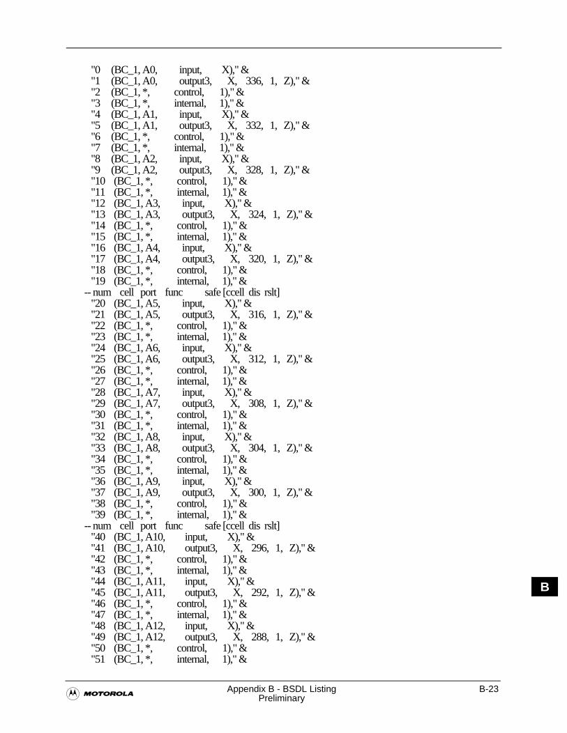
�Appendix B - BSDL Listing B-23
Preliminary
B
"0 (BC_1, A0, input, X)," & "1 (BC_1, A0, output3, X, 336, 1, Z)," & "2 (BC_1, *, control, 1)," & "3 (BC_1, *, internal, 1)," & "4 (BC_1, A1, input, X)," & "5 (BC_1, A1, output3, X, 332, 1, Z)," & "6 (BC_1, *, control, 1)," & "7 (BC_1, *, internal, 1)," & "8 (BC_1, A2, input, X)," & "9 (BC_1, A2, output3, X, 328, 1, Z)," & "10 (BC_1, *, control, 1)," & "11 (BC_1, *, internal, 1)," & "12 (BC_1, A3, input, X)," & "13 (BC_1, A3, output3, X, 324, 1, Z)," & "14 (BC_1, *, control, 1)," & "15 (BC_1, *, internal, 1)," & "16 (BC_1, A4, input, X)," & "17 (BC_1, A4, output3, X, 320, 1, Z)," & "18 (BC_1, *, control, 1)," & "19 (BC_1, *, internal, 1)," & -- num cell port func safe [ccell dis rslt] "20 (BC_1, A5, input, X)," & "21 (BC_1, A5, output3, X, 316, 1, Z)," & "22 (BC_1, *, control, 1)," & "23 (BC_1, *, internal, 1)," & "24 (BC_1, A6, input, X)," & "25 (BC_1, A6, output3, X, 312, 1, Z)," & "26 (BC_1, *, control, 1)," & "27 (BC_1, *, internal, 1)," & "28 (BC_1, A7, input, X)," & "29 (BC_1, A7, output3, X, 308, 1, Z)," & "30 (BC_1, *, control, 1)," & "31 (BC_1, *, internal, 1)," & "32 (BC_1, A8, input, X)," & "33 (BC_1, A8, output3, X, 304, 1, Z)," & "34 (BC_1, *, control, 1)," & "35 (BC_1, *, internal, 1)," & "36 (BC_1, A9, input, X)," & "37 (BC_1, A9, output3, X, 300, 1, Z)," & "38 (BC_1, *, control, 1)," & "39 (BC_1, *, internal, 1)," & -- num cell port func safe [ccell dis rslt] "40 (BC_1, A10, input, X)," & "41 (BC_1, A10, output3, X, 296, 1, Z)," & "42 (BC_1, *, control, 1)," & "43 (BC_1, *, internal, 1)," & "44 (BC_1, A11, input, X)," & "45 (BC_1, A11, output3, X, 292, 1, Z)," & "46 (BC_1, *, control, 1)," & "47 (BC_1, *, internal, 1)," & "48 (BC_1, A12, input, X)," & "49 (BC_1, A12, output3, X, 288, 1, Z)," & "50 (BC_1, *, control, 1)," & "51 (BC_1, *, internal, 1)," &
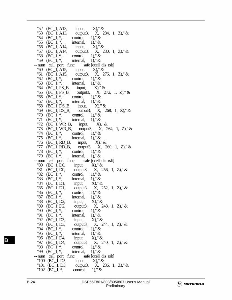
B-24 DSP56F801/803/805/807 User’s Manual�Preliminary
B
"52 (BC_1, A13, input, X)," & "53 (BC_1, A13, output3, X, 284, 1, Z)," & "54 (BC_1, *, control, 1)," & "55 (BC_1, *, internal, 1)," & "56 (BC_1, A14, input, X)," & "57 (BC_1, A14, output3, X, 280, 1, Z)," & "58 (BC_1, *, control, 1)," & "59 (BC_1, *, internal, 1)," & -- num cell port func safe [ccell dis rslt] "60 (BC_1, A15, input, X)," & "61 (BC_1, A15, output3, X, 276, 1, Z)," & "62 (BC_1, *, control, 1)," & "63 (BC_1, *, internal, 1)," & "64 (BC_1, PS_B, input, X)," & "65 (BC_1, PS_B, output3, X, 272, 1, Z)," & "66 (BC_1, *, control, 1)," & "67 (BC_1, *, internal, 1)," & "68 (BC_1, DS_B, input, X)," & "69 (BC_1, DS_B, output3, X, 268, 1, Z)," & "70 (BC_1, *, control, 1)," & "71 (BC_1, *, internal, 1)," & "72 (BC_1, WR_B, input, X)," & "73 (BC_1, WR_B, output3, X, 264, 1, Z)," & "74 (BC_1, *, control, 1)," & "75 (BC_1, *, internal, 1)," & "76 (BC_1, RD_B, input, X)," & "77 (BC_1, RD_B, output3, X, 260, 1, Z)," & "78 (BC_1, *, control, 1)," & "79 (BC_1, *, internal, 1)," & -- num cell port func safe [ccell dis rslt] "80 (BC_1, D0, input, X)," & "81 (BC_1, D0, output3, X, 256, 1, Z)," & "82 (BC_1, *, control, 1)," & "83 (BC_1, *, internal, 1)," & "84 (BC_1, D1, input, X)," & "85 (BC_1, D1, output3, X, 252, 1, Z)," & "86 (BC_1, *, control, 1)," & "87 (BC_1, *, internal, 1)," & "88 (BC_1, D2, input, X)," & "89 (BC_1, D2, output3, X, 248, 1, Z)," & "90 (BC_1, *, control, 1)," & "91 (BC_1, *, internal, 1)," & "92 (BC_1, D3, input, X)," & "93 (BC_1, D3, output3, X, 244, 1, Z)," & "94 (BC_1, *, control, 1)," & "95 (BC_1, *, internal, 1)," & "96 (BC_1, D4, input, X)," & "97 (BC_1, D4, output3, X, 240, 1, Z)," & "98 (BC_1, *, control, 1)," & "99 (BC_1, *, internal, 1)," & -- num cell port func safe [ccell dis rslt] "100 (BC_1, D5, input, X)," & "101 (BC_1, D5, output3, X, 236, 1, Z)," & "102 (BC_1, *, control, 1)," &
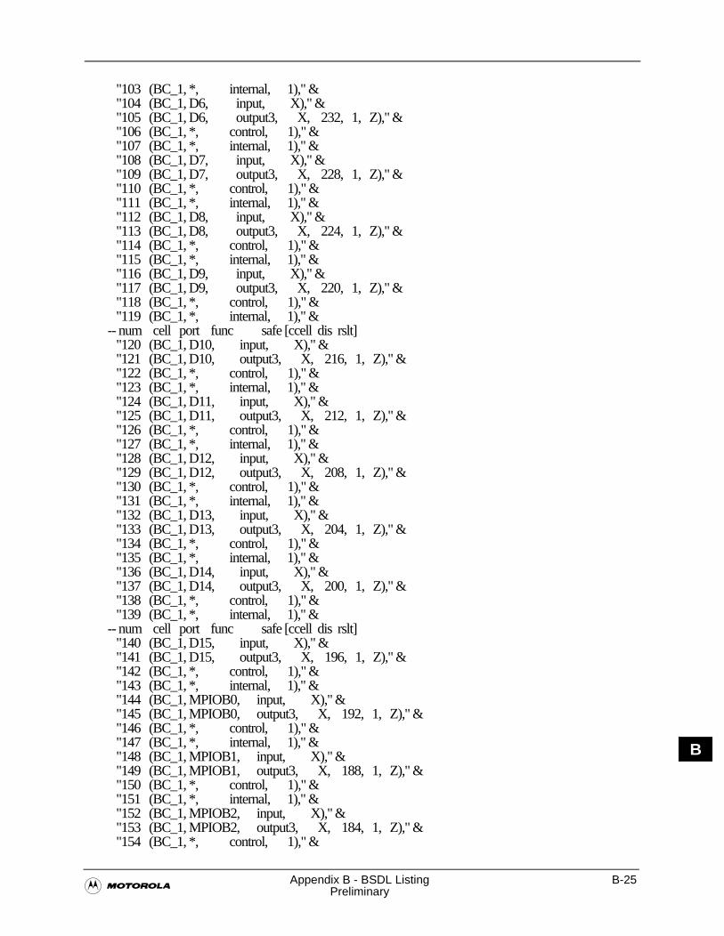
�Appendix B - BSDL Listing B-25
Preliminary
B
"103 (BC_1, *, internal, 1)," & "104 (BC_1, D6, input, X)," & "105 (BC_1, D6, output3, X, 232, 1, Z)," & "106 (BC_1, *, control, 1)," & "107 (BC_1, *, internal, 1)," & "108 (BC_1, D7, input, X)," & "109 (BC_1, D7, output3, X, 228, 1, Z)," & "110 (BC_1, *, control, 1)," & "111 (BC_1, *, internal, 1)," & "112 (BC_1, D8, input, X)," & "113 (BC_1, D8, output3, X, 224, 1, Z)," & "114 (BC_1, *, control, 1)," & "115 (BC_1, *, internal, 1)," & "116 (BC_1, D9, input, X)," & "117 (BC_1, D9, output3, X, 220, 1, Z)," & "118 (BC_1, *, control, 1)," & "119 (BC_1, *, internal, 1)," & -- num cell port func safe [ccell dis rslt] "120 (BC_1, D10, input, X)," & "121 (BC_1, D10, output3, X, 216, 1, Z)," & "122 (BC_1, *, control, 1)," & "123 (BC_1, *, internal, 1)," & "124 (BC_1, D11, input, X)," & "125 (BC_1, D11, output3, X, 212, 1, Z)," & "126 (BC_1, *, control, 1)," & "127 (BC_1, *, internal, 1)," & "128 (BC_1, D12, input, X)," & "129 (BC_1, D12, output3, X, 208, 1, Z)," & "130 (BC_1, *, control, 1)," & "131 (BC_1, *, internal, 1)," & "132 (BC_1, D13, input, X)," & "133 (BC_1, D13, output3, X, 204, 1, Z)," & "134 (BC_1, *, control, 1)," & "135 (BC_1, *, internal, 1)," & "136 (BC_1, D14, input, X)," & "137 (BC_1, D14, output3, X, 200, 1, Z)," & "138 (BC_1, *, control, 1)," & "139 (BC_1, *, internal, 1)," & -- num cell port func safe [ccell dis rslt] "140 (BC_1, D15, input, X)," & "141 (BC_1, D15, output3, X, 196, 1, Z)," & "142 (BC_1, *, control, 1)," & "143 (BC_1, *, internal, 1)," & "144 (BC_1, MPIOB0, input, X)," & "145 (BC_1, MPIOB0, output3, X, 192, 1, Z)," & "146 (BC_1, *, control, 1)," & "147 (BC_1, *, internal, 1)," & "148 (BC_1, MPIOB1, input, X)," & "149 (BC_1, MPIOB1, output3, X, 188, 1, Z)," & "150 (BC_1, *, control, 1)," & "151 (BC_1, *, internal, 1)," & "152 (BC_1, MPIOB2, input, X)," & "153 (BC_1, MPIOB2, output3, X, 184, 1, Z)," & "154 (BC_1, *, control, 1)," &
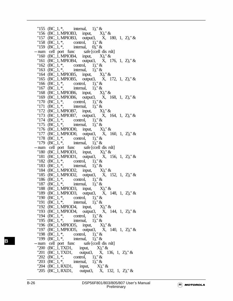
B-26 DSP56F801/803/805/807 User’s Manual�Preliminary
B
"155 (BC_1, *, internal, 1)," & "156 (BC_1, MPIOB3, input, X)," & "157 (BC_1, MPIOB3, output3, X, 180, 1, Z)," & "158 (BC_1, *, control, 1)," & "159 (BC_1, *, internal, 0)," & -- num cell port func safe [ccell dis rslt] "160 (BC_1, MPIOB4, input, X)," & "161 (BC_1, MPIOB4, output3, X, 176, 1, Z)," & "162 (BC_1, *, control, 1)," & "163 (BC_1, *, internal, 1)," & "164 (BC_1, MPIOB5, input, X)," & "165 (BC_1, MPIOB5, output3, X, 172, 1, Z)," & "166 (BC_1, *, control, 1)," & "167 (BC_1, *, internal, 1)," & "168 (BC_1, MPIOB6, input, X)," & "169 (BC_1, MPIOB6, output3, X, 168, 1, Z)," & "170 (BC_1, *, control, 1)," & "171 (BC_1, *, internal, 1)," & "172 (BC_1, MPIOB7, input, X)," & "173 (BC_1, MPIOB7, output3, X, 164, 1, Z)," & "174 (BC_1, *, control, 1)," & "175 (BC_1, *, internal, 1)," & "176 (BC_1, MPIOD0, input, X)," & "177 (BC_1, MPIOD0, output3, X, 160, 1, Z)," & "178 (BC_1, *, control, 1)," & "179 (BC_1, *, internal, 1)," & -- num cell port func safe [ccell dis rslt] "180 (BC_1, MPIOD1, input, X)," & "181 (BC_1, MPIOD1, output3, X, 156, 1, Z)," & "182 (BC_1, *, control, 1)," & "183 (BC_1, *, internal, 1)," & "184 (BC_1, MPIOD2, input, X)," & "185 (BC_1, MPIOD2, output3, X, 152, 1, Z)," & "186 (BC_1, *, control, 1)," & "187 (BC_1, *, internal, 1)," & "188 (BC_1, MPIOD3, input, X)," & "189 (BC_1, MPIOD3, output3, X, 148, 1, Z)," & "190 (BC_1, *, control, 1)," & "191 (BC_1, *, internal, 1)," & "192 (BC_1, MPIOD4, input, X)," & "193 (BC_1, MPIOD4, output3, X, 144, 1, Z)," & "194 (BC_1, *, control, 1)," & "195 (BC_1, *, internal, 1)," & "196 (BC_1, MPIOD5, input, X)," & "197 (BC_1, MPIOD5, output3, X, 140, 1, Z)," & "198 (BC_1, *, control, 1)," & "199 (BC_1, *, internal, 1)," & -- num cell port func safe [ccell dis rslt] "200 (BC_1, TXD1, input, X)," & "201 (BC_1, TXD1, output3, X, 136, 1, Z)," & "202 (BC_1, *, control, 1)," & "203 (BC_1, *, internal, 1)," & "204 (BC_1, RXD1, input, X)," & "205 (BC_1, RXD1, output3, X, 132, 1, Z)," &
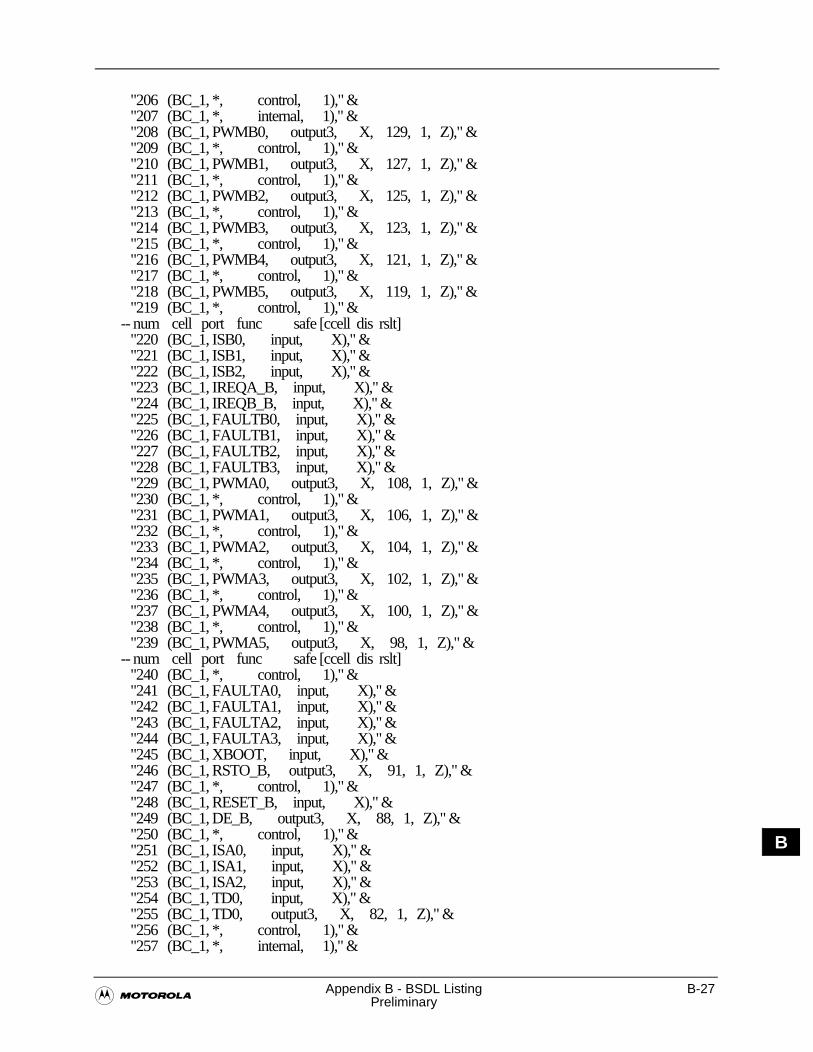
�Appendix B - BSDL Listing B-27
Preliminary
B
"206 (BC_1, *, control, 1)," & "207 (BC_1, *, internal, 1)," & "208 (BC_1, PWMB0, output3, X, 129, 1, Z)," & "209 (BC_1, *, control, 1)," & "210 (BC_1, PWMB1, output3, X, 127, 1, Z)," & "211 (BC_1, *, control, 1)," & "212 (BC_1, PWMB2, output3, X, 125, 1, Z)," & "213 (BC_1, *, control, 1)," & "214 (BC_1, PWMB3, output3, X, 123, 1, Z)," & "215 (BC_1, *, control, 1)," & "216 (BC_1, PWMB4, output3, X, 121, 1, Z)," & "217 (BC_1, *, control, 1)," & "218 (BC_1, PWMB5, output3, X, 119, 1, Z)," & "219 (BC_1, *, control, 1)," & -- num cell port func safe [ccell dis rslt] "220 (BC_1, ISB0, input, X)," & "221 (BC_1, ISB1, input, X)," & "222 (BC_1, ISB2, input, X)," & "223 (BC_1, IREQA_B, input, X)," & "224 (BC_1, IREQB_B, input, X)," & "225 (BC_1, FAULTB0, input, X)," & "226 (BC_1, FAULTB1, input, X)," & "227 (BC_1, FAULTB2, input, X)," & "228 (BC_1, FAULTB3, input, X)," & "229 (BC_1, PWMA0, output3, X, 108, 1, Z)," & "230 (BC_1, *, control, 1)," & "231 (BC_1, PWMA1, output3, X, 106, 1, Z)," & "232 (BC_1, *, control, 1)," & "233 (BC_1, PWMA2, output3, X, 104, 1, Z)," & "234 (BC_1, *, control, 1)," & "235 (BC_1, PWMA3, output3, X, 102, 1, Z)," & "236 (BC_1, *, control, 1)," & "237 (BC_1, PWMA4, output3, X, 100, 1, Z)," & "238 (BC_1, *, control, 1)," & "239 (BC_1, PWMA5, output3, X, 98, 1, Z)," & -- num cell port func safe [ccell dis rslt] "240 (BC_1, *, control, 1)," & "241 (BC_1, FAULTA0, input, X)," & "242 (BC_1, FAULTA1, input, X)," & "243 (BC_1, FAULTA2, input, X)," & "244 (BC_1, FAULTA3, input, X)," & "245 (BC_1, XBOOT, input, X)," & "246 (BC_1, RSTO_B, output3, X, 91, 1, Z)," & "247 (BC_1, *, control, 1)," & "248 (BC_1, RESET_B, input, X)," & "249 (BC_1, DE_B, output3, X, 88, 1, Z)," & "250 (BC_1, *, control, 1)," & "251 (BC_1, ISA0, input, X)," & "252 (BC_1, ISA1, input, X)," & "253 (BC_1, ISA2, input, X)," & "254 (BC_1, TD0, input, X)," & "255 (BC_1, TD0, output3, X, 82, 1, Z)," & "256 (BC_1, *, control, 1)," & "257 (BC_1, *, internal, 1)," &
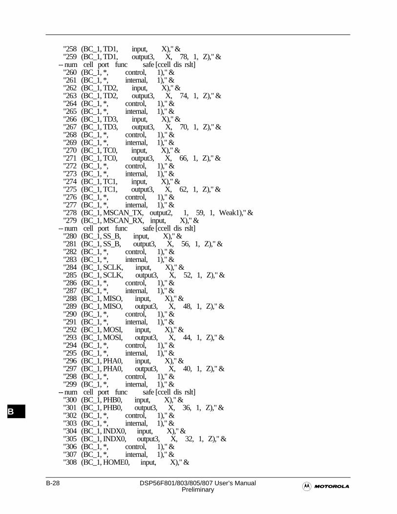
B-28 DSP56F801/803/805/807 User’s Manual�Preliminary
B
"258 (BC_1, TD1, input, X)," & "259 (BC_1, TD1, output3, X, 78, 1, Z)," & -- num cell port func safe [ccell dis rslt] "260 (BC_1, *, control, 1)," & "261 (BC_1, *, internal, 1)," & "262 (BC_1, TD2, input, X)," & "263 (BC_1, TD2, output3, X, 74, 1, Z)," & "264 (BC_1, *, control, 1)," & "265 (BC_1, *, internal, 1)," & "266 (BC_1, TD3, input, X)," & "267 (BC_1, TD3, output3, X, 70, 1, Z)," & "268 (BC_1, *, control, 1)," & "269 (BC_1, *, internal, 1)," & "270 (BC_1, TC0, input, X)," & "271 (BC_1, TC0, output3, X, 66, 1, Z)," & "272 (BC_1, *, control, 1)," & "273 (BC_1, *, internal, 1)," & "274 (BC_1, TC1, input, X)," & "275 (BC_1, TC1, output3, X, 62, 1, Z)," & "276 (BC_1, *, control, 1)," & "277 (BC_1, *, internal, 1)," & "278 (BC_1, MSCAN_TX, output2, 1, 59, 1, Weak1)," & "279 (BC_1, MSCAN_RX, input, X)," & -- num cell port func safe [ccell dis rslt] "280 (BC_1, SS_B, input, X)," & "281 (BC_1, SS_B, output3, X, 56, 1, Z)," & "282 (BC_1, *, control, 1)," & "283 (BC_1, *, internal, 1)," & "284 (BC_1, SCLK, input, X)," & "285 (BC_1, SCLK, output3, X, 52, 1, Z)," & "286 (BC_1, *, control, 1)," & "287 (BC_1, *, internal, 1)," & "288 (BC_1, MISO, input, X)," & "289 (BC_1, MISO, output3, X, 48, 1, Z)," & "290 (BC_1, *, control, 1)," & "291 (BC_1, *, internal, 1)," & "292 (BC_1, MOSI, input, X)," & "293 (BC_1, MOSI, output3, X, 44, 1, Z)," & "294 (BC_1, *, control, 1)," & "295 (BC_1, *, internal, 1)," & "296 (BC_1, PHA0, input, X)," & "297 (BC_1, PHA0, output3, X, 40, 1, Z)," & "298 (BC_1, *, control, 1)," & "299 (BC_1, *, internal, 1)," & -- num cell port func safe [ccell dis rslt] "300 (BC_1, PHB0, input, X)," & "301 (BC_1, PHB0, output3, X, 36, 1, Z)," & "302 (BC_1, *, control, 1)," & "303 (BC_1, *, internal, 1)," & "304 (BC_1, INDX0, input, X)," & "305 (BC_1, INDX0, output3, X, 32, 1, Z)," & "306 (BC_1, *, control, 1)," & "307 (BC_1, *, internal, 1)," & "308 (BC_1, HOME0, input, X)," &
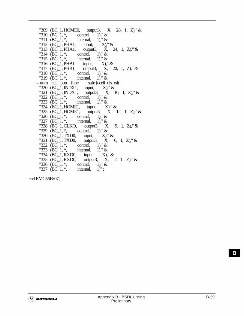
�Appendix B - BSDL Listing B-29
Preliminary
B
"309 (BC_1, HOME0, output3, X, 28, 1, Z)," & "310 (BC_1, *, control, 1)," & "311 (BC_1, *, internal, 1)," & "312 (BC_1, PHA1, input, X)," & "313 (BC_1, PHA1, output3, X, 24, 1, Z)," & "314 (BC_1, *, control, 1)," & "315 (BC_1, *, internal, 1)," & "316 (BC_1, PHB1, input, X)," & "317 (BC_1, PHB1, output3, X, 20, 1, Z)," & "318 (BC_1, *, control, 1)," & "319 (BC_1, *, internal, 1)," & -- num cell port func safe [ccell dis rslt] "320 (BC_1, INDX1, input, X)," & "321 (BC_1, INDX1, output3, X, 16, 1, Z)," & "322 (BC_1, *, control, 1)," & "323 (BC_1, *, internal, 1)," & "324 (BC_1, HOME1, input, X)," & "325 (BC_1, HOME1, output3, X, 12, 1, Z)," & "326 (BC_1, *, control, 1)," & "327 (BC_1, *, internal, 1)," & "328 (BC_1, CLKO, output3, X, 9, 1, Z)," & "329 (BC_1, *, control, 1)," & "330 (BC_1, TXD0, input, X)," & "331 (BC_1, TXD0, output3, X, 6, 1, Z)," & "332 (BC_1, *, control, 1)," & "333 (BC_1, *, internal, 1)," & "334 (BC_1, RXD0, input, X)," & "335 (BC_1, RXD0, output3, X, 2, 1, Z)," & "336 (BC_1, *, control, 1)," & "337 (BC_1, *, internal, 1)" ;
end EMC56F807;

B-30 DSP56F801/803/805/807 User’s Manual�Preliminary
B

�Appendix C - Programmer’s Sheets C-1
Preliminary
C
Appendix CProgrammer’s Sheets

C-2 DSP56F801/803/805/807 User’s Manual�Preliminary
C
�Appendix C - Programmer’s Sheets C-3
Preliminary
C
Appendix CProgrammer’s Sheets
C.1 Introduction
The following pages provide a set of reference tables and programming sheets intended to simplify programming the DSP56F801/803/805/807. The programming sheets provide room to write in the value of each bit and the hexadecimal value for each register. The programmer can photocopy these sheets. (Copy at 122% to enlarge these pages to a full 8-1/2” x 11”.)
C.2 Instruction Set Summary
The following tables provide brief summaries of the instruction set for the DSP56F801/803/805/807. For complete instruction set details, refer to Appendix A of the DSP56800 Family Manual.
Each described instruction contains notations used to abbreviate certain operands and operations described in Table C-7. Keys to the symbols and their respective descriptions of the Set Instructions located in Table C-7 are listed in Table C-1 through C-6.
Table C-2 illustrates the register set available for the most important move instruction. Sometimes the register field is broken into two different fields--one where the register is used as a source and the other where it is used as a destination. This is important because a different notation is used when an accumulator is being stored without saturation.
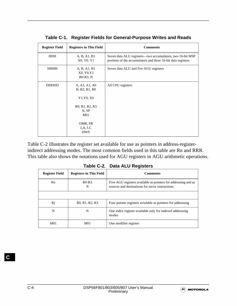
C-4 DSP56F801/803/805/807 User’s Manual�Preliminary
C
Table C-2 illustrates the register set available for use as pointers in address-register- indirect addressing modes. The most common fields used in this table are Rn and RRR. This table also shows the notations used for AGU registers in AGU arithmetic operations.
Table C-2. Data ALU Registers
Table C-1. Register Fields for General-Purpose Writes and Reads
Register Field Registers in This Field Comments
HHH A, B, A1, B1X0, Y0, Y1
Seven data ALU registers---two accumulators, two 16-bit MSP portions of the accumulators and three 16-bit data registers
HHHH A, B, A1, B1X0, Y0,Y1R0-R3, N
Seven data ALU and five AGU registers
DDDDD A, A2, A1, A0B, B2, B1, B0
Y1,Y0, X0
R0, R1, R2, R3N, SPM01
OMR, SRLA, LCHWS
All CPU registers
Register Field Registers in This Field Comments
Rn R0-R3N
Five AGU registers available as pointers for addressing and as sources and destinations for move instructions
Rj R0, R1, R2, R3 Four pointer registers avialable as pointers for addressing
N N One index register available only for indexed addressing modes
M01 M01 One modifier register
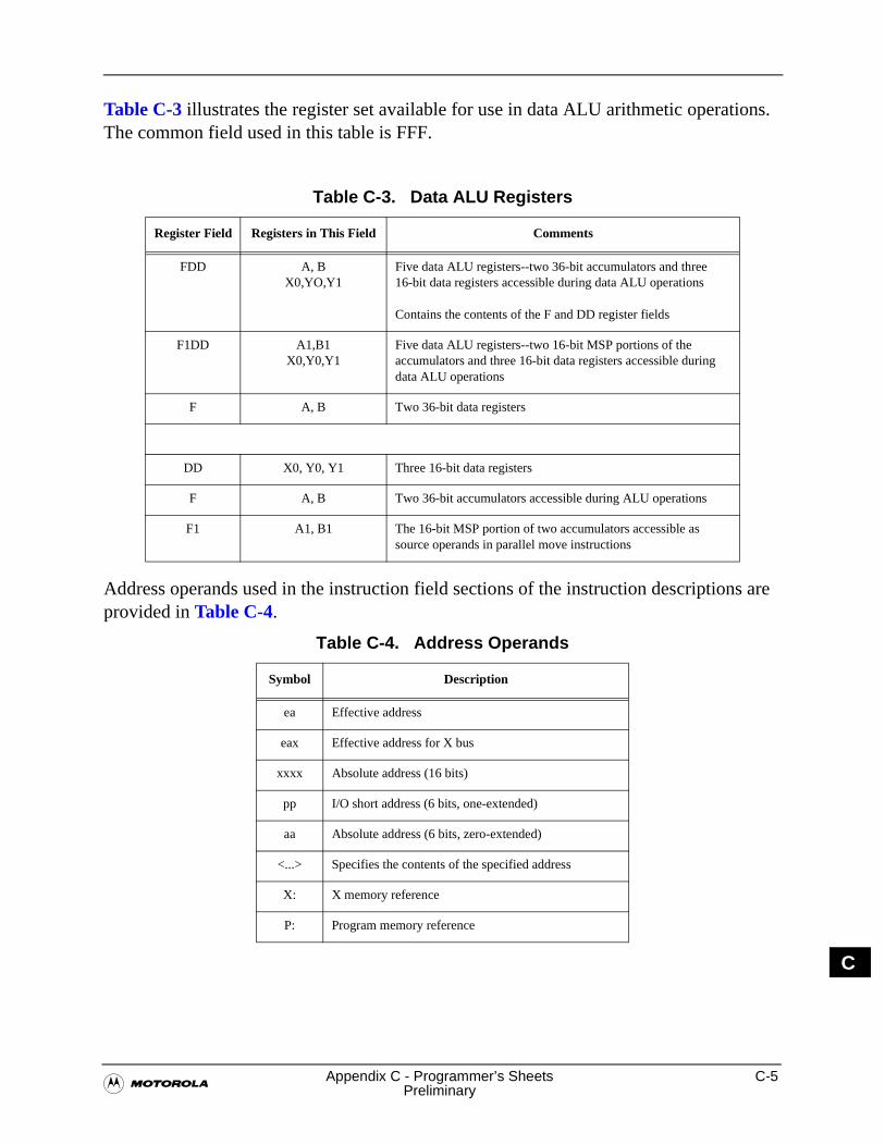
�Appendix C - Programmer’s Sheets C-5
Preliminary
C
Table C-3 illustrates the register set available for use in data ALU arithmetic operations. The common field used in this table is FFF.
Address operands used in the instruction field sections of the instruction descriptions are provided in Table C-4.
Table C-3. Data ALU Registers
Register Field Registers in This Field Comments
FDD A, BX0,YO,Y1
Five data ALU registers--two 36-bit accumulators and three 16-bit data registers accessible during data ALU operations
Contains the contents of the F and DD register fields
F1DD A1,B1X0,Y0,Y1
Five data ALU registers--two 16-bit MSP portions of the accumulators and three 16-bit data registers accessible during data ALU operations
F A, B Two 36-bit data registers
DD X0, Y0, Y1 Three 16-bit data registers
F A, B Two 36-bit accumulators accessible during ALU operations
F1 A1, B1 The 16-bit MSP portion of two accumulators accessible as source operands in parallel move instructions
Table C-4. Address Operands
Symbol Description
ea Effective address
eax Effective address for X bus
xxxx Absolute address (16 bits)
pp I/O short address (6 bits, one-extended)
aa Absolute address (6 bits, zero-extended)
<...> Specifies the contents of the specified address
X: X memory reference
P: Program memory reference
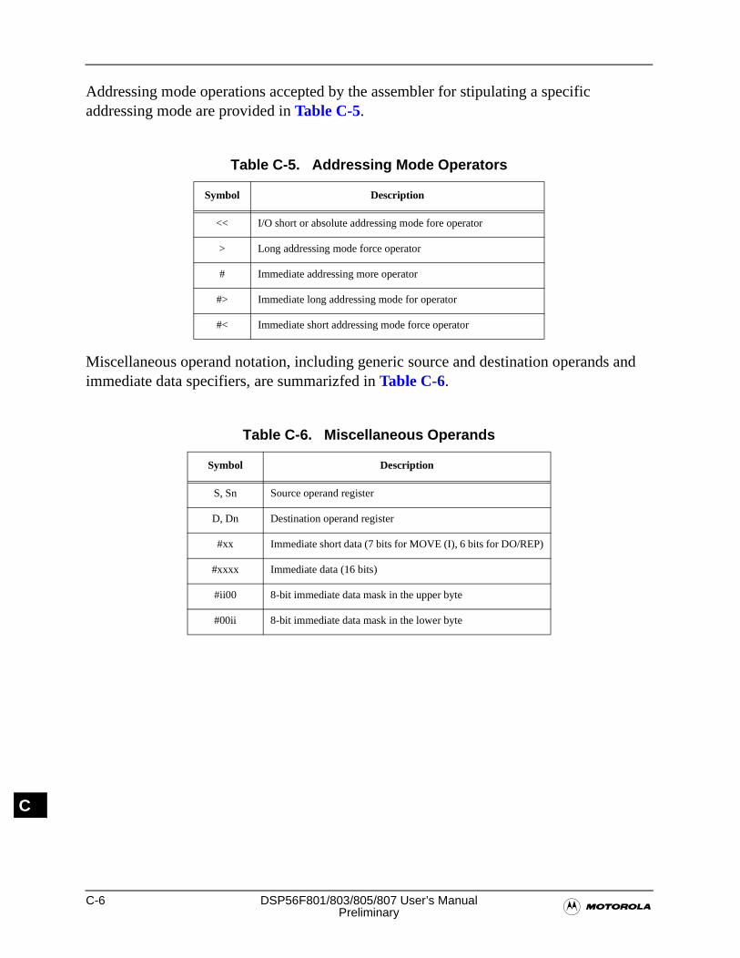
C-6 DSP56F801/803/805/807 User’s Manual�Preliminary
C
Addressing mode operations accepted by the assembler for stipulating a specific addressing mode are provided in Table C-5.
Miscellaneous operand notation, including generic source and destination operands and immediate data specifiers, are summarizfed in Table C-6.
Table C-5. Addressing Mode Operators
Symbol Description
<< I/O short or absolute addressing mode fore operator
> Long addressing mode force operator
# Immediate addressing more operator
#> Immediate long addressing mode for operator
#< Immediate short addressing mode force operator
Table C-6. Miscellaneous Operands
Symbol Description
S, Sn Source operand register
D, Dn Destination operand register
#xx Immediate short data (7 bits for MOVE (I), 6 bits for DO/REP)
#xxxx Immediate data (16 bits)
#ii00 8-bit immediate data mask in the upper byte
#00ii 8-bit immediate data mask in the lower byte
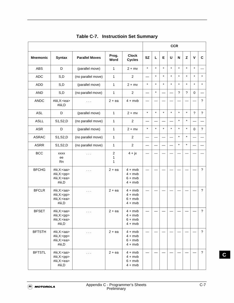
�Appendix C - Programmer’s Sheets C-7
Preliminary
C
Table C-7. Instructioin Set Summary
CCR
Mnemonic Syntax Parallel MovesProg.Word
ClockCycles
SZ L E U N Z V C
ABS D (parallel move) 1 2 + mv * * * * * * * —
ADC S,D (no parallel move) 1 2 — * * * * * * *
ADD S,D (parallel move) 1 2 + mv * * * * * * * *
AND S,D (no parallel move) 1 2 — * — — ? ? 0 —
ANDC #iiii,X:<ea>#iiii,D
. . . 2 + ea 4 + mvb — — — — — — — ?
ASL D (parallel move) 1 2 + mv * * * * * * ? ?
ASLL S1,S2,D (no parallel move) 1 2 — — — — * * — —
ASR D (parallel move) 1 2 + mv * * * * * * 0 ?
ASRAC S1,S2,D (no parallel move) 1 2 — — — — * * — —
ASRR S1,S2,D (no parallel move) 1 2 — — — — * * — —
BCC xxxxeeRn
. . . 211
4 + jx — — — — — — — —
BFCHG #iii,X:<aa>#iii,X:<pp>#iii,X:<ea>
#iii,D
. . . 2 + ea 4 + mvb4 + mvb6 + mvb4 + mvb
— — — — — — — ?
BFCLR #iii,X:<aa>#iii,X:<pp>#iii,X:<ea>
#iii,D
. . . 2 + ea 4 + mvb4 + mvb6 + mvb4 + mvb
— — — — — — — ?
BFSET #iii,X:<aa>#iii,X:<pp>#iii,X:<ea>
#iii,D
. . . 2 + ea 4 + mvb4 + mvb6 + mvb4 + mvb
— — — — — — — ?
BFTSTH #iii,X:<aa>#iii,X:<pp>#iii,X:<ea>
#iii,D
. . . 2 + ea 4 + mvb4 + mvb6 + mvb4 + mvb
— — — — — — — ?
BFTSTL #iii,X:<aa>#iii,X:<pp>#iii,X:<ea>
#iii,D
. . . 2 + ea 4 + mvb4 + mvb6 + mvb4 + mvb
— — — — — — — ?
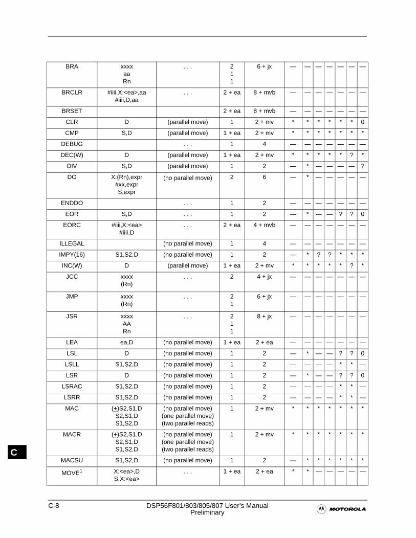
C-8 DSP56F801/803/805/807 User’s Manual�Preliminary
C
BRA xxxxaaRn
. . . 211
6 + jx — — — — — — —
BRCLR #iiii,X:<ea>,aa#iiii,D,aa
. . . 2 + ea 8 + mvb — — — — — — —
BRSET 2 + ea 8 + mvb — — — — — — —
CLR D (parallel move) 1 2 + mv * * * * * * 0
CMP S,D (parallel move) 1 + ea 2 + mv * * * * * * *
DEBUG . . . 1 4 — — — — — — —
DEC(W) D (parallel move) 1 + ea 2 + mv * * * * * ? *
DIV S,D (parallel move) 1 2 — * — — — — ?
DO X:(Rn),expr#xx,exprS,expr
(no parallel move) 2 6 — * — — — — —
ENDDO . . . 1 2 — — — — — — —
EOR S,D . . . 1 2 — * — — ? ? 0
EORC #iiii,X:<ea>#iiii,D
. . . 2 + ea 4 + mvb — — — — — — —
ILLEGAL (no parallel move) 1 4 — — — — — — —
IMPY(16) S1,S2,D (no parallel move) 1 2 — * ? ? * * *
INC(W) D (parallel move) 1 + ea 2 + mv * * * * * ? *
JCC xxxx(Rn)
. . . 2 4 + jx — — — — — — —
JMP xxxx(Rn)
. . . 21
6 + jx — — — — — — —
JSR xxxxAARn
. . . 211
8 + jx — — — — — — —
LEA ea,D (no parallel move) 1 + ea 2 + ea — — — — — — —
LSL D (no parallel move) 1 2 — * — — ? ? 0
LSLL S1,S2,D (no parallel move) 1 2 — — — — * * —
LSR D (no parallel move) 1 2 — * — — ? ? 0
LSRAC S1,S2,D (no parallel move) 1 2 — — — — * * —
LSRR S1,S2,D (no parallel move) 1 2 — — — — * * —
MAC (+)S2,S1,DS2,S1,DS1,S2,D
(no parallel move)(one parallel move)(two parallel reads)
1 2 + mv * * * * * * *
MACR (+)S2,S1,DS2,S1,DS1,S2,D
(no parallel move)(one parallel move)(two parallel reads)
1 2 + mv * * * * * * *
MACSU S1,S2,D (no parallel move) 1 2 — * * * * * *
MOVE1 X:<ea>,DS,X:<ea>
. . . 1 + ea 2 + ea * * — — — — —
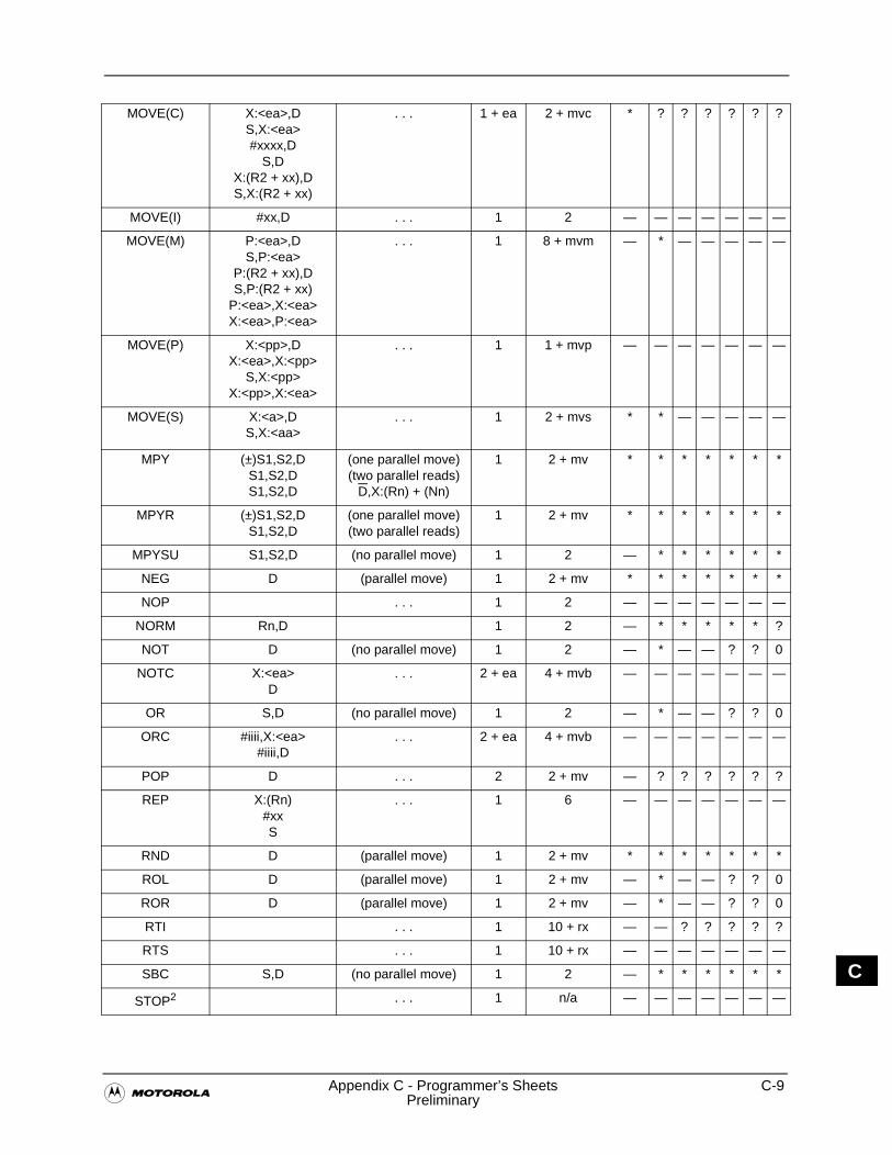
�Appendix C - Programmer’s Sheets C-9
Preliminary
C
MOVE(C) X:<ea>,DS,X:<ea>#xxxx,D
S,DX:(R2 + xx),DS,X:(R2 + xx)
. . . 1 + ea 2 + mvc * ? ? ? ? ? ?
MOVE(I) #xx,D . . . 1 2 — — — — — — —
MOVE(M) P:<ea>,DS,P:<ea>
P:(R2 + xx),DS,P:(R2 + xx)
P:<ea>,X:<ea>X:<ea>,P:<ea>
. . . 1 8 + mvm — * — — — — —
MOVE(P) X:<pp>,DX:<ea>,X:<pp>
S,X:<pp>X:<pp>,X:<ea>
. . . 1 1 + mvp — — — — — — —
MOVE(S) X:<a>,DS,X:<aa>
. . . 1 2 + mvs * * — — — — —
MPY (±)S1,S2,DS1,S2,DS1,S2,D
(one parallel move)(two parallel reads)
D,X:(Rn) + (Nn)
1 2 + mv * * * * * * *
MPYR (±)S1,S2,DS1,S2,D
(one parallel move)(two parallel reads)
1 2 + mv * * * * * * *
MPYSU S1,S2,D (no parallel move) 1 2 — * * * * * *
NEG D (parallel move) 1 2 + mv * * * * * * *
NOP . . . 1 2 — — — — — — —
NORM Rn,D 1 2 — * * * * * ?
NOT D (no parallel move) 1 2 — * — — ? ? 0
NOTC X:<ea>D
. . . 2 + ea 4 + mvb — — — — — — —
OR S,D (no parallel move) 1 2 — * — — ? ? 0
ORC #iiii,X:<ea>#iiii,D
. . . 2 + ea 4 + mvb — — — — — — —
POP D . . . 2 2 + mv — ? ? ? ? ? ?
REP X:(Rn)#xxS
. . . 1 6 — — — — — — —
RND D (parallel move) 1 2 + mv * * * * * * *
ROL D (parallel move) 1 2 + mv — * — — ? ? 0
ROR D (parallel move) 1 2 + mv — * — — ? ? 0
RTI . . . 1 10 + rx — — ? ? ? ? ?
RTS . . . 1 10 + rx — — — — — — —
SBC S,D (no parallel move) 1 2 — * * * * * *
STOP2 . . . 1 n/a — — — — — — —
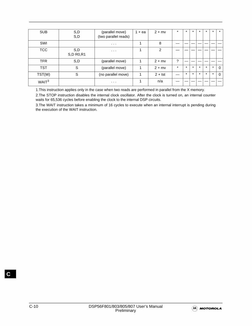
C-10 DSP56F801/803/805/807 User’s Manual�Preliminary
C
SUB S,DS,D
(parallel move)(two parallel reads)
1 + ea 2 + mv * * * * * * *
SWI . . . 1 8 — — — — — — —
TCC S,DS,D R0,R1
. . . 1 2 — — — — — — —
TFR S,D (parallel move) 1 2 + mv ? — — — — — —
TST S (parallel move) 1 2 + mv * * * * * * 0
TST(W) S (no parallel move) 1 2 + tst — * * * * * 0
WAIT3 . . . 1 n/a — — — — — — —
1.This instruction applies only in the case when two reads are performed in parallel from the X memory.
2.The STOP instruction disables the internal clock oscillator. After the clock is turned on, an internal counterwaits for 65,536 cycles before enabling the clock to the internal DSP circuits.
3.The WAIT instruction takes a minimum of 16 cycles to execute when an internal interrupt is pending duringthe execution of the WAIT instruction.
�Appendix C - Programmer’s Sheets C-11
Preliminary
C
C.3 Interrupt, Vector, and Address TablesRefer to Chapter 3, Section 3.5 and 3.10 for interrupt, vector, and address tables. Table titles are listed below.
Table 3-11 Data Memory Peripheral Address MapTable 3-12 System Control Registers Address MapTable 3-13 Program Flash Interface Unit #2 Registers Address MapTable 3-14 Quad Timer A Registers Address MapTable 3-15 Quad Timer B Registers Address MapTable 3-16 Quad Timer C Registers Address MapTable 3-17 Quad Timer D Registers Address MapTable 3-18 CAN Registers Address MapTable 3-19 PWMA Registers Address MapTable 3-20 PWMB Registers Address MapTable 3-21 Quadrature Decoder #0 Registers Address MapTable 3-22 Quadrature Decoder #1 Registers Address MapTable 3-23 Interrupt Controller Registers Address MapTable 3-24 ADCA Registers Address MapTable 3-24 ADCA Registers Address MapTable 3-25 ADCB Registers Address MapTable 3-26 SCI0 Registers Address MapTable 3-27 SCI1 Registers Address MapTable 3-28 SPI Registers Address MapTable 3-29 COP Registers Address MapTable 3-30 Program Flash Interface Unit Registers Address MapTable 3-31 Data Flash Interface Unit Registers Address MapTable 3-32 Boot Flash Interface Unit Registers Address MapTable 3-33 Clock Generation Registers Address MapTable 3-34 GPIO Port A Registers Address MapTable 3-35 GPIO Port B Registers Address MapTable 3-36 GPIO Port D Registers Address MapTable 3-37 GPIO Port E Registers Address MapTable 3-38 DSP56F801/803/805/807 Program Memory Chip Operating ModesTable 3-39 Example Contents of Data Stream to be Loaded from Serial EEPROMTable 3-40 Reset and Interrupt Priority StructureTable 3-41 Reset and Interrupt Vector Map
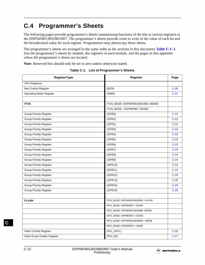
C-12 DSP56F801/803/805/807 User’s Manual�Preliminary
C
C.4 Programmer’s SheetsThe following pages provide programmer’s sheets summarizing functions of the bits in various registers in the DSP56F801/803/805/807. The programmer’s sheets provide room to write in the value of each bit and the hexadecimal value for each register. Programmers may photocopy these sheets.
The programmer’s sheets are arranged in the same order as the sections in this document. Table C-C-1 lists the programmer’s sheets by module, the registers in each module, and the pages in this appendix where the programmer’s sheets are located.
Note: Reserved bits should only be set to zero unless otherwise stated. •
Table C-1. List of Programmer’s Sheets
RegisterType Register Page
CPU Registers
Bus Control Register (BCR) C-20
Operating Mode Register (OMR) C-21
ITCN ITCN_BASE: DSP56F801/803/805 =$0E60
ITCN_BASE: DSP56F807 =$1260
Group Priority Register (GPR0) C-22
Group Priority Register (GPR1) C-22
Group Priority Register (GPR2) C-22
Group Priority Register (GPR3) C-22
Group Priority Register (GPR4) C-23
Group Priority Register (GPR5) C-23
Group Priority Register (GPR6) C-23
Group Priority Register (GPR7) C-23
Group Priority Register (GPR8) C-24
Group Priority Register (GPR9) C-24
Group Priority Register (GPR10) C-24
Group Priority Register (GPR11) C-24
Group Priority Register (GPR12) C-25
Group Priority Register (GPR13) C-25
Group Priority Register (GPR14) C-25
Group Priority Register (GPR15) C-25
FLASH PFIU_BASE: DSP56F801/803/805 = $ 0F40
PFIU_BASE: DSP56F807 = $1340
DFIU_BASE: DSP56F801/803/805 =$0F60
DFIU_BASE: DSP56F807 = $1360
BFIU_BASE: DSP56F801/803/805 = $0F80
BFIU_BASE: DSP56F807 = $1380
Flash Control Register (FIU_CNTL) C-26
Flash Erase Enable Register (FIU_EE) C-27
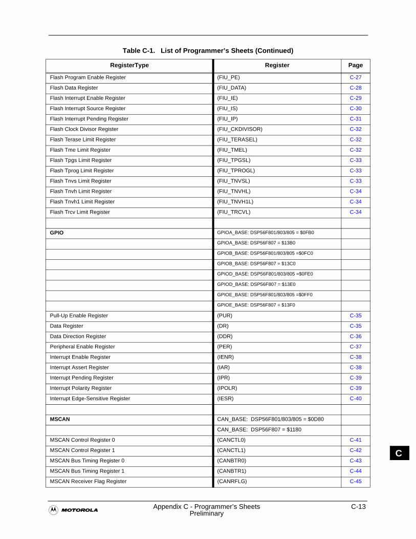
�Appendix C - Programmer’s Sheets C-13
Preliminary
C
Flash Program Enable Register (FIU_PE) C-27
Flash Data Register (FIU_DATA) C-28
Flash Interrupt Enable Register (FIU_IE) C-29
Flash Interrupt Source Register (FIU_IS) C-30
Flash Interrupt Pending Register (FIU_IP) C-31
Flash Clock Divisor Register (FIU_CKDIVISOR) C-32
Flash Terase Limit Register (FIU_TERASEL) C-32
Flash Tme Limit Register (FIU_TMEL) C-32
Flash Tpgs Limit Register (FIU_TPGSL) C-33
Flash Tprog Limit Register (FIU_TPROGL) C-33
Flash Tnvs Limit Register (FIU_TNVSL) C-33
Flash Tnvh Limit Register (FIU_TNVHL) C-34
Flash Tnvh1 Limit Register (FIU_TNVH1L) C-34
Flash Trcv Limit Register (FIU_TRCVL) C-34
GPIO GPIOA_BASE: DSP56F801/803/805 = $0FB0
GPIOA_BASE: DSP56F807 = $13B0
GPIOB_BASE: DSP56F801/803/805 =$0FC0
GPIOB_BASE: DSP56F807 = $13C0
GPIOD_BASE: DSP56F801/803/805 =$0FE0
GPIOD_BASE: DSP56F807 = $13E0
GPIOE_BASE: DSP56F801/803/805 =$0FF0
GPIOE_BASE: DSP56F807 = $13F0
Pull-Up Enable Register (PUR) C-35
Data Register (DR) C-35
Data Direction Register (DDR) C-36
Peripheral Enable Register (PER) C-37
Interrupt Enable Register (IENR) C-38
Interrupt Assert Register (IAR) C-38
Interrupt Pending Register (IPR) C-39
Interrupt Polarity Register (IPOLR) C-39
Interrupt Edge-Sensitive Register (IESR) C-40
MSCAN CAN_BASE: DSP56F801/803/805 = $0D80
CAN_BASE: DSP56F807 = $1180
MSCAN Control Register 0 (CANCTL0) C-41
MSCAN Control Register 1 (CANCTL1) C-42
MSCAN Bus Timing Register 0 (CANBTR0) C-43
MSCAN Bus Timing Register 1 (CANBTR1) C-44
MSCAN Receiver Flag Register (CANRFLG) C-45
Table C-1. List of Programmer’s Sheets (Continued)
RegisterType Register Page
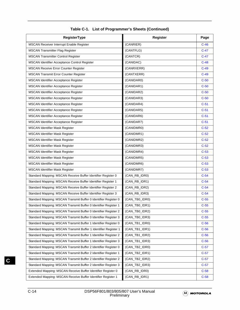
C-14 DSP56F801/803/805/807 User’s Manual�Preliminary
C
MSCAN Receiver Interrupt Enable Register (CANRIER) C-46
MSCAN Transmitter Flag Register (CANTFLG) C-47
MSCAN Transmitter Control Register (CANTCR) C-47
MSCAN Identifier Acceptance Control Register (CANIDAC) C-48
MSCAN Receive Error Counter Register (CANRXERR) C-49
MSCAN Transmit Error Counter Register (CANTXERR) C-49
MSCAN Identifier Acceptance Register (CANIDAR0) C-50
MSCAN Identifier Acceptance Register (CANIDAR1) C-50
MSCAN Identifier Acceptance Register (CANIDAR2) C-50
MSCAN Identifier Acceptance Register (CANIDAR3) C-50
MSCAN Identifier Acceptance Register (CANIDAR4) C-51
MSCAN Identifier Acceptance Register (CANIDAR5) C-51
MSCAN Identifier Acceptance Register (CANIDAR6) C-51
MSCAN Identifier Acceptance Register (CANIDAR7) C-51
MSCAN Identifier Mask Register (CANIDMR0) C-52
MSCAN Identifier Mask Register (CANIDMR1) C-52
MSCAN Identifier Mask Register (CANIDMR2) C-52
MSCAN Identifier Mask Register (CANIDMR3) C-52
MSCAN Identifier Mask Register (CANIDMR4) C-53
MSCAN Identifier Mask Register (CANIDMR5) C-53
MSCAN Identifier Mask Register (CANIDMR6) C-53
MSCAN Identifier Mask Register (CANIDMR7) C-53
Standard Mapping: MSCAN Receive Buffer Identifier Register 0 (CAN_RB_IDR0) C-54
Standard Mapping: MSCAN Receive Buffer Identifier Register 1 (CAN_RB_IDR1) C-54
Standard Mapping: MSCAN Receive Buffer Identifier Register 2 (CAN_RB_IDR2) C-54
Standard Mapping: MSCAN Receive Buffer Identifier Register 3 (CAN_RB_IDR3) C-54
Standard Mapping: MSCAN Transmit Buffer 0 Identifier Register 0 (CAN_TB0_IDR0) C-55
Standard Mapping: MSCAN Transmit Buffer 0 Identifier Register 1 (CAN_TB0_IDR1) C-55
Standard Mapping: MSCAN Transmit Buffer 0 Identifier Register 2 (CAN_TB0_IDR2) C-55
Standard Mapping: MSCAN Transmit Buffer 0 Identifier Register 3 (CAN_TB0_IDR3) C-55
Standard Mapping: MSCAN Transmit Buffer 1 Identifier Register 0 (CAN_TB1_IDR0) C-56
Standard Mapping: MSCAN Transmit Buffer 1 Identifier Register 1 (CAN_TB1_IDR1) C-56
Standard Mapping: MSCAN Transmit Buffer 1 Identifier Register 2 (CAN_TB1_IDR2) C-56
Standard Mapping: MSCAN Transmit Buffer 1 Identifier Register 3 (CAN_TB1_IDR3) C-56
Standard Mapping: MSCAN Transmit Buffer 2 Identifier Register 0 (CAN_TB2_IDR0) C-57
Standard Mapping: MSCAN Transmit Buffer 2 Identifier Register 1 (CAN_TB2_IDR1) C-57
Standard Mapping: MSCAN Transmit Buffer 2 Identifier Register 2 (CAN_TB2_IDR2) C-57
Standard Mapping: MSCAN Transmit Buffer 2 Identifier Register 3 (CAN_TB2_IDR3) C-57
Extended Mapping: MSCAN Receive Buffer Identifier Register 0 (CAN_RB_IDR0) C-58
Extended Mapping: MSCAN Receive Buffer Identifier Register 1 (CAN_RB_IDR1) C-58
Table C-1. List of Programmer’s Sheets (Continued)
RegisterType Register Page
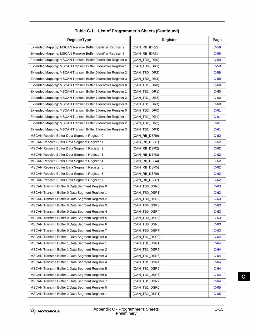
�Appendix C - Programmer’s Sheets C-15
Preliminary
C
Extended Mapping: MSCAN Receive Buffer Identifier Register 2 (CAN_RB_IDR2) C-58
Extended Mapping: MSCAN Receive Buffer Identifier Register 3 (CAN_RB_IDR3) C-58
Extended Mapping: MSCAN Transmit Buffer 0 Identifier Register 0 (CAN_TB0_IDR0) C-59
Extended Mapping: MSCAN Transmit Buffer 0 Identifier Register 1 (CAN_TB0_IDR1) C-59
Extended Mapping: MSCAN Transmit Buffer 0 Identifier Register 2 (CAN_TB0_IDR2) C-59
Extended Mapping: MSCAN Transmit Buffer 0 Identifier Register 3 (CAN_TB0_IDR3) C-59
Extended Mapping: MSCAN Transmit Buffer 1 Identifier Register 0 (CAN_TB1_IDR0) C-60
Extended Mapping: MSCAN Transmit Buffer 1 Identifier Register 1 (CAN_TB1_IDR1) C-60
Extended Mapping: MSCAN Transmit Buffer 1 Identifier Register 2 (CAN_TB1_IDR2) C-60
Extended Mapping: MSCAN Transmit Buffer 1 Identifier Register 3 (CAN_TB1_IDR3) C-60
Extended Mapping: MSCAN Transmit Buffer 2 Identifier Register 0 (CAN_TB2_IDR0) C-61
Extended Mapping: MSCAN Transmit Buffer 2 Identifier Register 1 (CAN_TB2_IDR1) C-61
Extended Mapping: MSCAN Transmit Buffer 2 Identifier Register 2 (CAN_TB2_IDR2) C-61
Extended Mapping: MSCAN Transmit Buffer 2 Identifier Register 3 (CAN_TB2_IDR3) C-61
MSCAN Receive Buffer Data Segment Register 0 (CAN_RB_DSR0) C-62
MSCAN Receive Buffer Data Segment Register 1 (CAN_RB_DSR1) C-62
MSCAN Receive Buffer Data Segment Register 2 (CAN_RB_DSR2) C-62
MSCAN Receive Buffer Data Segment Register 3 (CAN_RB_DSR3) C-62
MSCAN Receive Buffer Data Segment Register 4 (CAN_RB_DSR4) C-62
MSCAN Receive Buffer Data Segment Register 5 (CAN_RB_DSR5) C-62
MSCAN Receive Buffer Data Segment Register 6 (CAN_RB_DSR6) C-62
MSCAN Receive Buffer Data Segment Register 7 (CAN_RB_DSR7) C-62
MSCAN Transmit Buffer 0 Data Segment Register 0 (CAN_TB0_DSR0) C-63
MSCAN Transmit Buffer 0 Data Segment Register 1 (CAN_TB0_DSR1) C-63
MSCAN Transmit Buffer 0 Data Segment Register 2 (CAN_TB0_DSR2) C-63
MSCAN Transmit Buffer 0 Data Segment Register 3 (CAN_TB0_DSR3) C-63
MSCAN Transmit Buffer 0 Data Segment Register 4 (CAN_TB0_DSR4) C-63
MSCAN Transmit Buffer 0 Data Segment Register 5 (CAN_TB0_DSR5) C-63
MSCAN Transmit Buffer 0 Data Segment Register 6 (CAN_TB0_DSR6) C-63
MSCAN Transmit Buffer 0 Data Segment Register 7 (CAN_TB0_DSR7) C-63
MSCAN Transmit Buffer 1 Data Segment Register 0 (CAN_TB1_DSR0) C-64
MSCAN Transmit Buffer 1 Data Segment Register 1 (CAN_TB1_DSR1) C-64
MSCAN Transmit Buffer 1 Data Segment Register 2 (CAN_TB1_DSR2) C-64
MSCAN Transmit Buffer 1 Data Segment Register 3 (CAN_TB1_DSR3) C-64
MSCAN Transmit Buffer 1 Data Segment Register 4 (CAN_TB1_DSR4) C-64
MSCAN Transmit Buffer 1 Data Segment Register 5 (CAN_TB1_DSR5) C-64
MSCAN Transmit Buffer 1 Data Segment Register 6 (CAN_TB1_DSR6) C-64
MSCAN Transmit Buffer 1 Data Segment Register 7 (CAN_TB1_DSR7) C-64
MSCAN Transmit Buffer 2 Data Segment Register 0 (CAN_TB2_DSR0) C-65
MSCAN Transmit Buffer 2 Data Segment Register 1 (CAN_TB2_DSR1) C-65
Table C-1. List of Programmer’s Sheets (Continued)
RegisterType Register Page
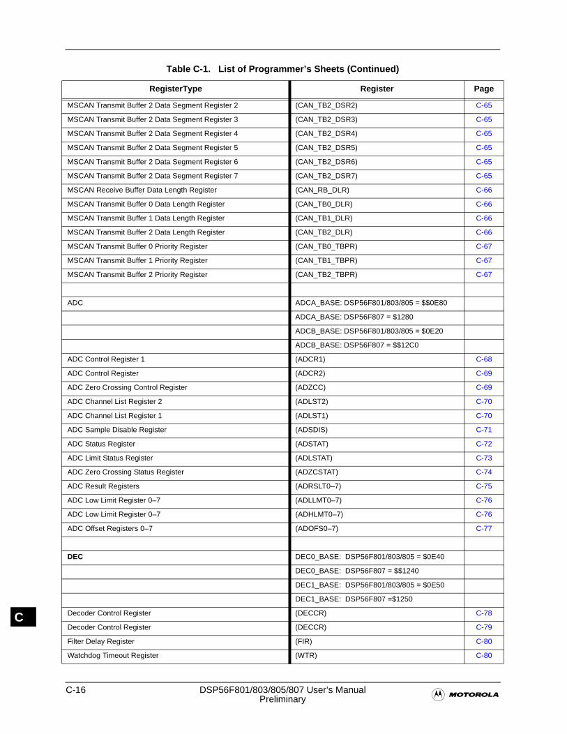
C-16 DSP56F801/803/805/807 User’s Manual�Preliminary
C
MSCAN Transmit Buffer 2 Data Segment Register 2 (CAN_TB2_DSR2) C-65
MSCAN Transmit Buffer 2 Data Segment Register 3 (CAN_TB2_DSR3) C-65
MSCAN Transmit Buffer 2 Data Segment Register 4 (CAN_TB2_DSR4) C-65
MSCAN Transmit Buffer 2 Data Segment Register 5 (CAN_TB2_DSR5) C-65
MSCAN Transmit Buffer 2 Data Segment Register 6 (CAN_TB2_DSR6) C-65
MSCAN Transmit Buffer 2 Data Segment Register 7 (CAN_TB2_DSR7) C-65
MSCAN Receive Buffer Data Length Register (CAN_RB_DLR) C-66
MSCAN Transmit Buffer 0 Data Length Register (CAN_TB0_DLR) C-66
MSCAN Transmit Buffer 1 Data Length Register (CAN_TB1_DLR) C-66
MSCAN Transmit Buffer 2 Data Length Register (CAN_TB2_DLR) C-66
MSCAN Transmit Buffer 0 Priority Register (CAN_TB0_TBPR) C-67
MSCAN Transmit Buffer 1 Priority Register (CAN_TB1_TBPR) C-67
MSCAN Transmit Buffer 2 Priority Register (CAN_TB2_TBPR) C-67
ADC ADCA_BASE: DSP56F801/803/805 = $$0E80
ADCA_BASE: DSP56F807 = $1280
ADCB_BASE: DSP56F801/803/805 = $0E20
ADCB_BASE: DSP56F807 = $$12C0
ADC Control Register 1 (ADCR1) C-68
ADC Control Register (ADCR2) C-69
ADC Zero Crossing Control Register (ADZCC) C-69
ADC Channel List Register 2 (ADLST2) C-70
ADC Channel List Register 1 (ADLST1) C-70
ADC Sample Disable Register (ADSDIS) C-71
ADC Status Register (ADSTAT) C-72
ADC Limit Status Register (ADLSTAT) C-73
ADC Zero Crossing Status Register (ADZCSTAT) C-74
ADC Result Registers (ADRSLT0–7) C-75
ADC Low Limit Register 0–7 (ADLLMT0–7) C-76
ADC Low Limit Register 0–7 (ADHLMT0–7) C-76
ADC Offset Registers 0–7 (ADOFS0–7) C-77
DEC DEC0_BASE: DSP56F801/803/805 = $0E40
DEC0_BASE: DSP56F807 = $$1240
DEC1_BASE: DSP56F801/803/805 = $0E50
DEC1_BASE: DSP56F807 =$1250
Decoder Control Register (DECCR) C-78
Decoder Control Register (DECCR) C-79
Filter Delay Register (FIR) C-80
Watchdog Timeout Register (WTR) C-80
Table C-1. List of Programmer’s Sheets (Continued)
RegisterType Register Page
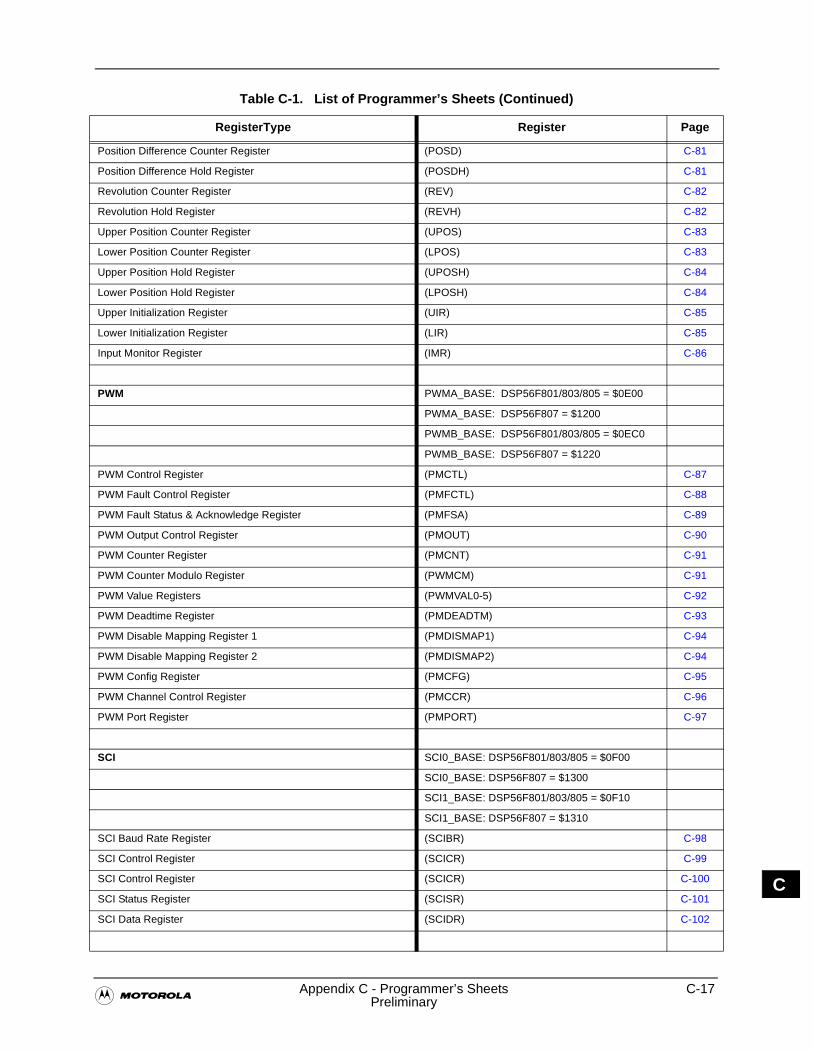
�Appendix C - Programmer’s Sheets C-17
Preliminary
C
Position Difference Counter Register (POSD) C-81
Position Difference Hold Register (POSDH) C-81
Revolution Counter Register (REV) C-82
Revolution Hold Register (REVH) C-82
Upper Position Counter Register (UPOS) C-83
Lower Position Counter Register (LPOS) C-83
Upper Position Hold Register (UPOSH) C-84
Lower Position Hold Register (LPOSH) C-84
Upper Initialization Register (UIR) C-85
Lower Initialization Register (LIR) C-85
Input Monitor Register (IMR) C-86
PWM PWMA_BASE: DSP56F801/803/805 = $0E00
PWMA_BASE: DSP56F807 = $1200
PWMB_BASE: DSP56F801/803/805 = $0EC0
PWMB_BASE: DSP56F807 = $1220
PWM Control Register (PMCTL) C-87
PWM Fault Control Register (PMFCTL) C-88
PWM Fault Status & Acknowledge Register (PMFSA) C-89
PWM Output Control Register (PMOUT) C-90
PWM Counter Register (PMCNT) C-91
PWM Counter Modulo Register (PWMCM) C-91
PWM Value Registers (PWMVAL0-5) C-92
PWM Deadtime Register (PMDEADTM) C-93
PWM Disable Mapping Register 1 (PMDISMAP1) C-94
PWM Disable Mapping Register 2 (PMDISMAP2) C-94
PWM Config Register (PMCFG) C-95
PWM Channel Control Register (PMCCR) C-96
PWM Port Register (PMPORT) C-97
SCI SCI0_BASE: DSP56F801/803/805 = $0F00
SCI0_BASE: DSP56F807 = $1300
SCI1_BASE: DSP56F801/803/805 = $0F10
SCI1_BASE: DSP56F807 = $1310
SCI Baud Rate Register (SCIBR) C-98
SCI Control Register (SCICR) C-99
SCI Control Register (SCICR) C-100
SCI Status Register (SCISR) C-101
SCI Data Register (SCIDR) C-102
Table C-1. List of Programmer’s Sheets (Continued)
RegisterType Register Page
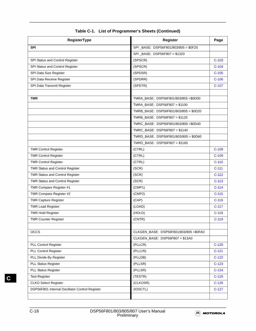
C-18 DSP56F801/803/805/807 User’s Manual�Preliminary
C
SPI SPI _BASE: DSP56F801/803/805 = $0F20
SPI _BASE: DSP56F807 = $1320
SPI Status and Control Register (SPSCR) C-103
SPI Status and Control Register (SPSCR) C-104
SPI Data Size Register (SPDSR) C-105
SPI Data Receive Register (SPDRR) C-106
SPI Data Transmit Register (SPDTR) C-107
TMR TMRA_BASE: DSP56F801/803/805 =$0D00
TMRA_BASE: DSP56F807 = $1100
TMRB_BASE: DSP56F801/803/805 = $0D20
TMRB_BASE: DSP56F807 = $1120
TMRC_BASE: DSP56F801/803/805 =$0D40
TMRC_BASE: DSP56F807 = $1140
TMRD_BASE: DSP56F801/803/805 = $0D60
TMRD_BASE: DSP56F807 = $1160
TMR Control Register (CTRL) C-108
TMR Control Register (CTRL) C-109
TMR Control Register (CTRL) C-110
TMR Status and Control Register (SCR) C-111
TMR Status and Control Register (SCR) C-112
TMR Status and Control Register (SCR) C-113
TMR Compare Register #1 (CMP1) C-114
TMR Compare Register #2 (CMP2) C-115
TMR Capture Register (CAP) C-116
TMR Load Register (LOAD) C-117
TMR Hold Register (HOLD) C-118
TMR Counter Register (CNTR) C-119
OCCS CLKGEN_BASE: DSP56F801/803/805 =$0FA0
CLKGEN_BASE: DSP56F807 = $13A0
PLL Control Register (PLLCR) C-120
PLL Control Register (PLLCR) C-121
PLL Divide-By Register (PLLDB) C-122
PLL Status Register (PLLSR) C-123
PLL Status Register (PLLSR) C-124
Test Register (TESTR) C-125
CLKO Select Register (CLKOSR) C-126
DSP56F801 Internal Oscillator Control Register (IOSCTL) C-127
Table C-1. List of Programmer’s Sheets (Continued)
RegisterType Register Page
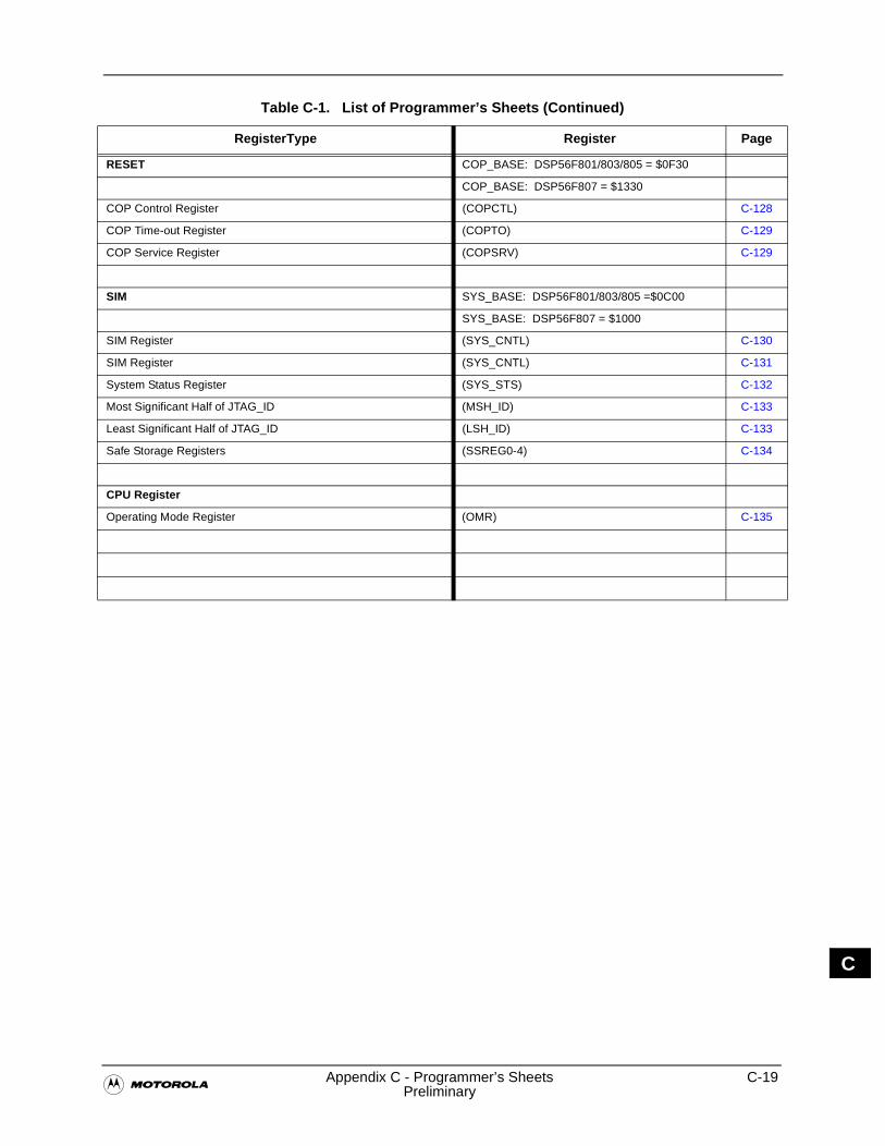
�Appendix C - Programmer’s Sheets C-19
Preliminary
C
RESET COP_BASE: DSP56F801/803/805 = $0F30
COP_BASE: DSP56F807 = $1330
COP Control Register (COPCTL) C-128
COP Time-out Register (COPTO) C-129
COP Service Register (COPSRV) C-129
SIM SYS_BASE: DSP56F801/803/805 =$0C00
SYS_BASE: DSP56F807 = $1000
SIM Register (SYS_CNTL) C-130
SIM Register (SYS_CNTL) C-131
System Status Register (SYS_STS) C-132
Most Significant Half of JTAG_ID (MSH_ID) C-133
Least Significant Half of JTAG_ID (LSH_ID) C-133
Safe Storage Registers (SSREG0-4) C-134
CPU Register
Operating Mode Register (OMR) C-135
Table C-1. List of Programmer’s Sheets (Continued)
RegisterType Register Page
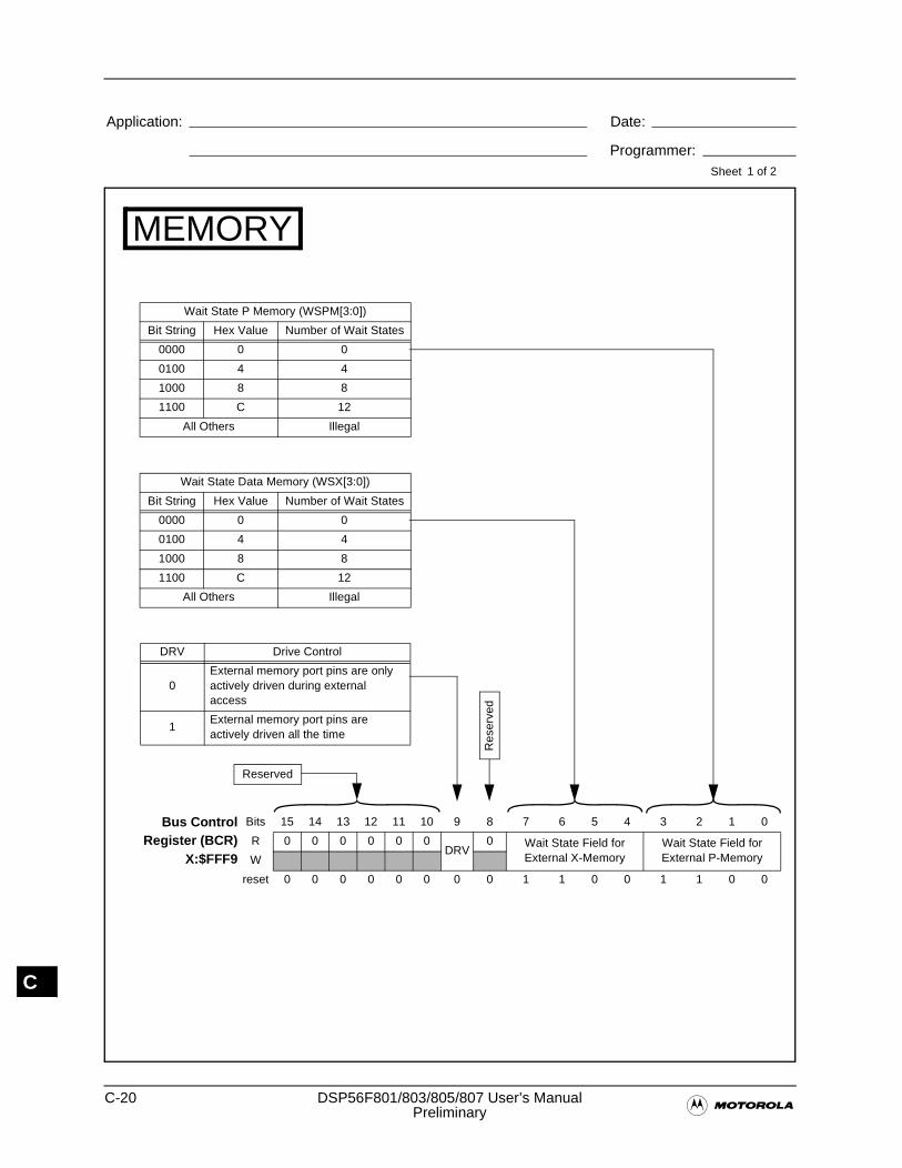
C-20 DSP56F801/803/805/807 User’s Manual�Preliminary
Application: Date:
Programmer:Sheet
C
Wait State Data Memory (WSX[3:0])
Bit String Hex Value Number of Wait States
0000 0 0
0100 4 4
1000 8 8
1100 C 12
All Others Illegal
Wait State P Memory (WSPM[3:0])
Bit String Hex Value Number of Wait States
0000 0 0
0100 4 4
1000 8 8
1100 C 12
All Others Illegal
DRV Drive Control
0External memory port pins are only actively driven during external access
1External memory port pins are actively driven all the time
Bus ControlRegister (BCR)
X:$FFF9
Bits 15 14 13 12 11 10 9 8 7 6 5 4 3 2 1 0
R 0 0 0 0 0 0DRV
0 Wait State Field for External X-Memory
Wait State Field for External P-MemoryW
reset 0 0 0 0 0 0 0 0 1 1 0 0 1 1 0 0
Reserved
1 of 2
MEMORY
Res
erve
d
Appendix C
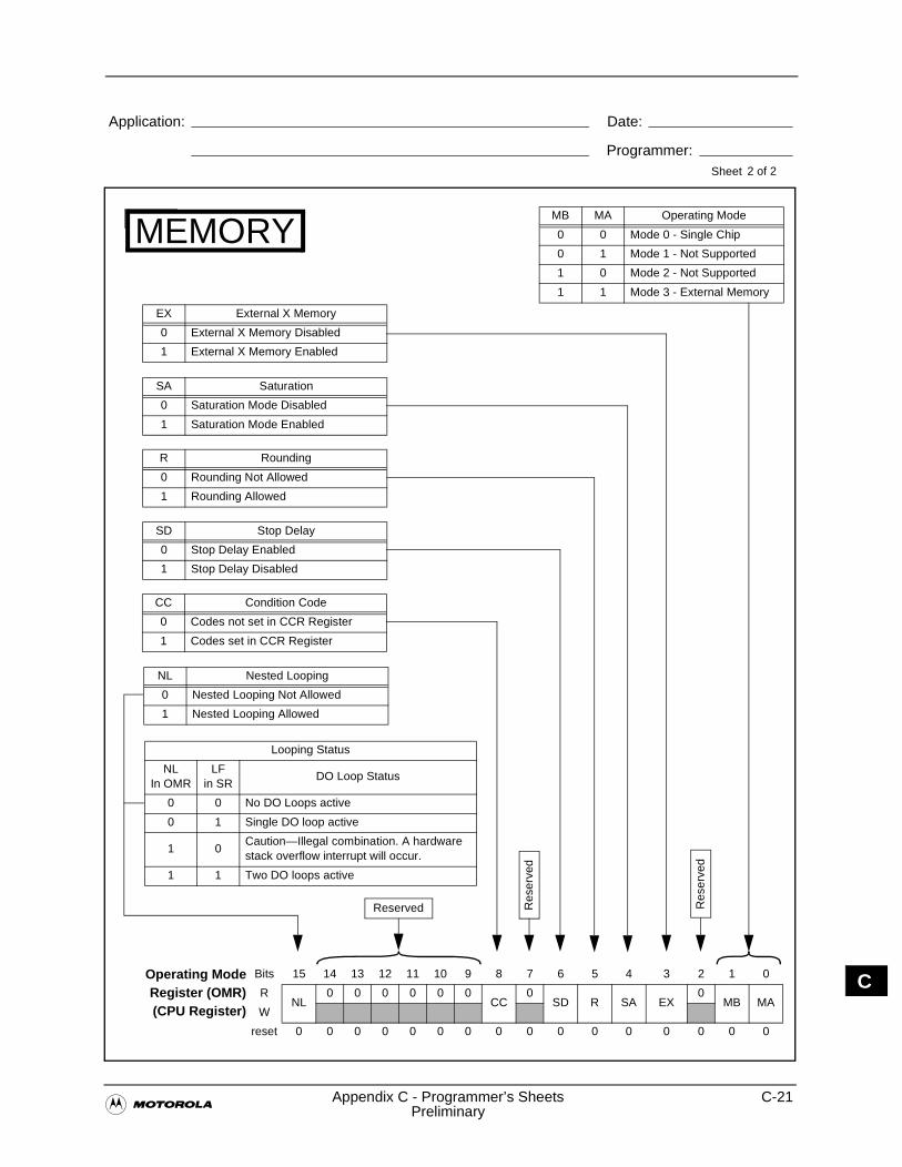
�Appendix C - Programmer’s Sheets C-21
Preliminary
Application: Date:
Programmer:Sheet
C
MEMORY
2 of 2
Operating ModeRegister (OMR)(CPU Register)
Bits 15 14 13 12 11 10 9 8 7 6 5 4 3 2 1 0
RNL
0 0 0 0 0 0CC
0SD R SA EX
0MB MA
W
reset 0 0 0 0 0 0 0 0 0 0 0 0 0 0 0 0
Looping Status
NL In OMR
LFin SR
DO Loop Status
0 0 No DO Loops active
0 1 Single DO loop active
1 0Caution—Illegal combination. A hardware stack overflow interrupt will occur.
1 1 Two DO loops active
CC Condition Code
0 Codes not set in CCR Register
1 Codes set in CCR Register
SD Stop Delay
0 Stop Delay Enabled
1 Stop Delay Disabled
R Rounding
0 Rounding Not Allowed
1 Rounding Allowed
SA Saturation
0 Saturation Mode Disabled
1 Saturation Mode Enabled
EX External X Memory
0 External X Memory Disabled
1 External X Memory Enabled
Reserved
MB MA Operating Mode
0 0 Mode 0 - Single Chip
0 1 Mode 1 - Not Supported
1 0 Mode 2 - Not Supported
1 1 Mode 3 - External Memory
Res
erve
d
Res
erve
d
NL Nested Looping
0 Nested Looping Not Allowed
1 Nested Looping Allowed
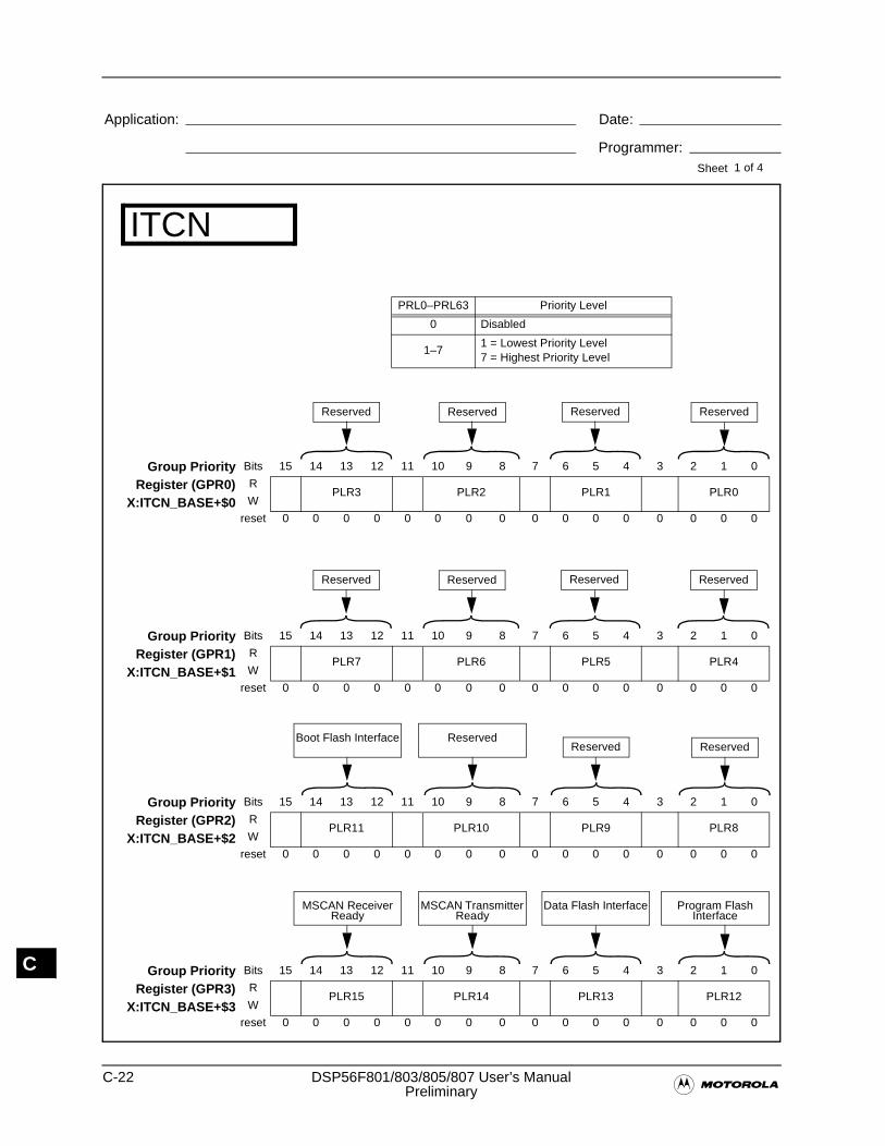
C-22 DSP56F801/803/805/807 User’s Manual�Preliminary
Application: Date:
Programmer:Sheet
C
1 of 4
ITCN
Group PriorityRegister (GPR0)
X:ITCN_BASE+$0
Bits 15 14 13 12 11 10 9 8 7 6 5 4 3 2 1 0
RPLR3 PLR2 PLR1 PLR0
W
reset 0 0 0 0 0 0 0 0 0 0 0 0 0 0 0 0
Reserved Reserved Reserved Reserved
Group PriorityRegister (GPR1)
X:ITCN_BASE+$1
Bits 15 14 13 12 11 10 9 8 7 6 5 4 3 2 1 0
RPLR7 PLR6 PLR5 PLR4
W
reset 0 0 0 0 0 0 0 0 0 0 0 0 0 0 0 0
Reserved Reserved Reserved
Group PriorityRegister (GPR2)
X:ITCN_BASE+$2
Bits 15 14 13 12 11 10 9 8 7 6 5 4 3 2 1 0
RPLR11 PLR10 PLR9 PLR8
W
reset 0 0 0 0 0 0 0 0 0 0 0 0 0 0 0 0
Reserved Reserved
Group PriorityRegister (GPR3)
X:ITCN_BASE+$3
Bits 15 14 13 12 11 10 9 8 7 6 5 4 3 2 1 0
RPLR15 PLR14 PLR13 PLR12
W
reset 0 0 0 0 0 0 0 0 0 0 0 0 0 0 0 0
Program Flash Interface
Data Flash InterfaceMSCAN Transmitter Ready
MSCAN Receiver Ready
ReservedBoot Flash Interface
PRL0–PRL63 Priority Level
0 Disabled
1–71 = Lowest Priority Level7 = Highest Priority Level
Reserved
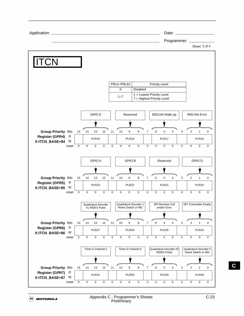
�Appendix C - Programmer’s Sheets C-23
Preliminary
Application: Date:
Programmer:Sheet
C
Quadrature Decoder #1 INDEX Pulse
2 of 4
ITCN
Group PriorityRegister (GPR7)
X:ITCN_BASE+$7
Bits 15 14 13 12 11 10 9 8 7 6 5 4 3 2 1 0
RPLR31 PLR30 PLR29 PLR28
W
reset 0 0 0 0 0 0 0 0 0 0 0 0 0 0 0 0
Quadrature Decoder 0 Home Switch or WD
Quadrature Decoder #0 INDEX Pulse
Timer D Channel 0Timer D Channel 1
PRL0–PRL63 Priority Level
0 Disabled
1–71 = Lowest Priority Level7 = Highest Priority Level
Group PriorityRegister (GPR4)
X:ITCN_BASE+$4
Bits 15 14 13 12 11 10 9 8 7 6 5 4 3 2 1 0
RPLR19 PLR18 PLR17 PLR16
W
reset 0 0 0 0 0 0 0 0 0 0 0 0 0 0 0 0
MSCAN ErrorMSCAN Walk-upReservedGPIO E
Group PriorityRegister (GPR5)
X:ITCN_BASE+$5
Bits 15 14 13 12 11 10 9 8 7 6 5 4 3 2 1 0
RPLR23 PLR22 PLR21 PLR20
W
reset 0 0 0 0 0 0 0 0 0 0 0 0 0 0 0 0
GPIO DReservedGPIO BGPIO A
Group PriorityRegister (GPR6)
X:ITCN_BASE+$6
Bits 15 14 13 12 11 10 9 8 7 6 5 4 3 2 1 0
RPLR27 PLR26 PLR25 PLR24
W
reset 0 0 0 0 0 0 0 0 0 0 0 0 0 0 0 0
SPI Transmitter EmptySPI Receiver Fulland/or Error
Quadrature Decoder 1 Home Switch or WD
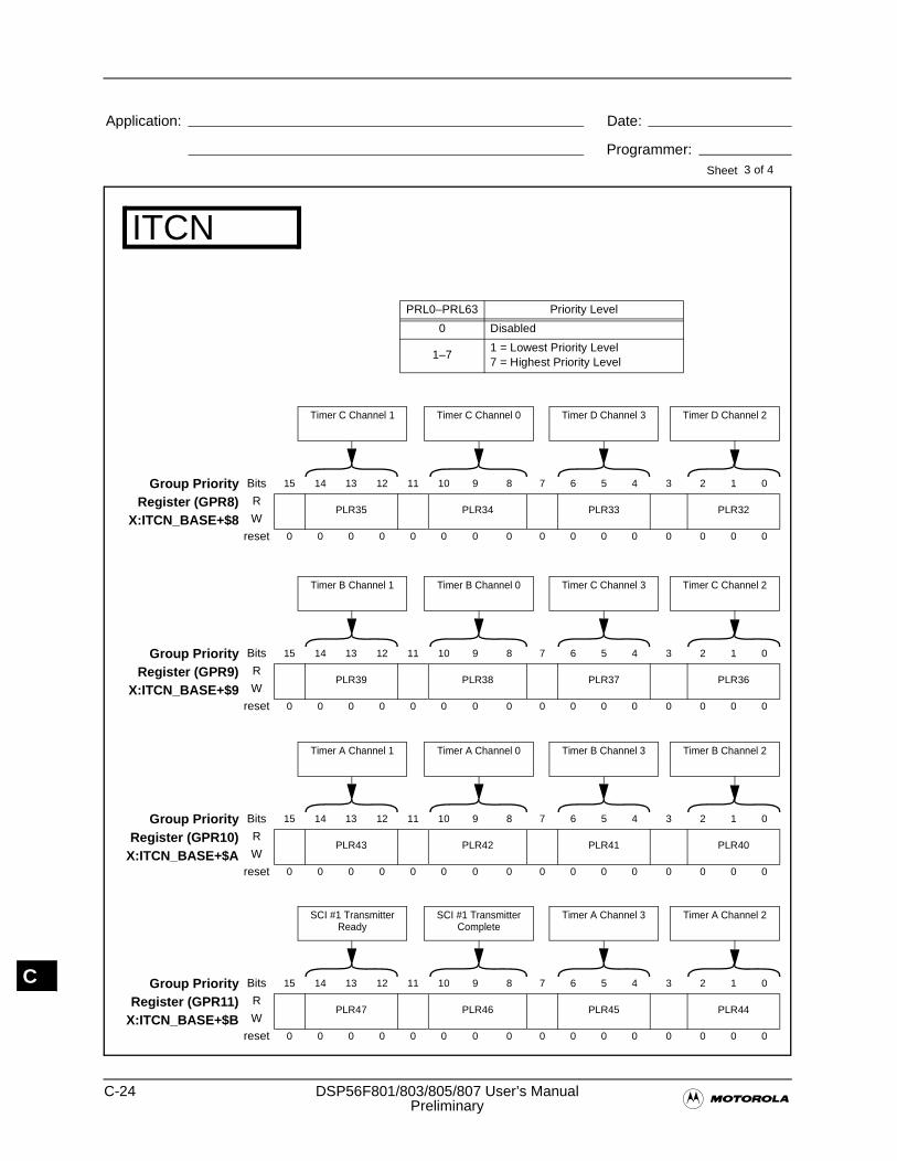
C-24 DSP56F801/803/805/807 User’s Manual�Preliminary
Application: Date:
Programmer:Sheet
C
3 of 4
ITCN
Group PriorityRegister (GPR11)
X:ITCN_BASE+$B
Bits 15 14 13 12 11 10 9 8 7 6 5 4 3 2 1 0
RPLR47 PLR46 PLR45 PLR44
W
reset 0 0 0 0 0 0 0 0 0 0 0 0 0 0 0 0
Timer A Channel 2Timer A Channel 3SCI #1 Transmitter Complete
SCI #1 Transmitter Ready
PRL0–PRL63 Priority Level
0 Disabled
1–71 = Lowest Priority Level7 = Highest Priority Level
Group PriorityRegister (GPR8)
X:ITCN_BASE+$8
Bits 15 14 13 12 11 10 9 8 7 6 5 4 3 2 1 0
RPLR35 PLR34 PLR33 PLR32
W
reset 0 0 0 0 0 0 0 0 0 0 0 0 0 0 0 0
Timer D Channel 2Timer D Channel 3Timer C Channel 0Timer C Channel 1
Group PriorityRegister (GPR9)
X:ITCN_BASE+$9
Bits 15 14 13 12 11 10 9 8 7 6 5 4 3 2 1 0
RPLR39 PLR38 PLR37 PLR36
W
reset 0 0 0 0 0 0 0 0 0 0 0 0 0 0 0 0
Timer C Channel 2Timer C Channel 3Timer B Channel 0Timer B Channel 1
Group PriorityRegister (GPR10)
X:ITCN_BASE+$A
Bits 15 14 13 12 11 10 9 8 7 6 5 4 3 2 1 0
RPLR43 PLR42 PLR41 PLR40
W
reset 0 0 0 0 0 0 0 0 0 0 0 0 0 0 0 0
Timer B Channel 2Timer B Channel 3Timer A Channel 0Timer A Channel 1
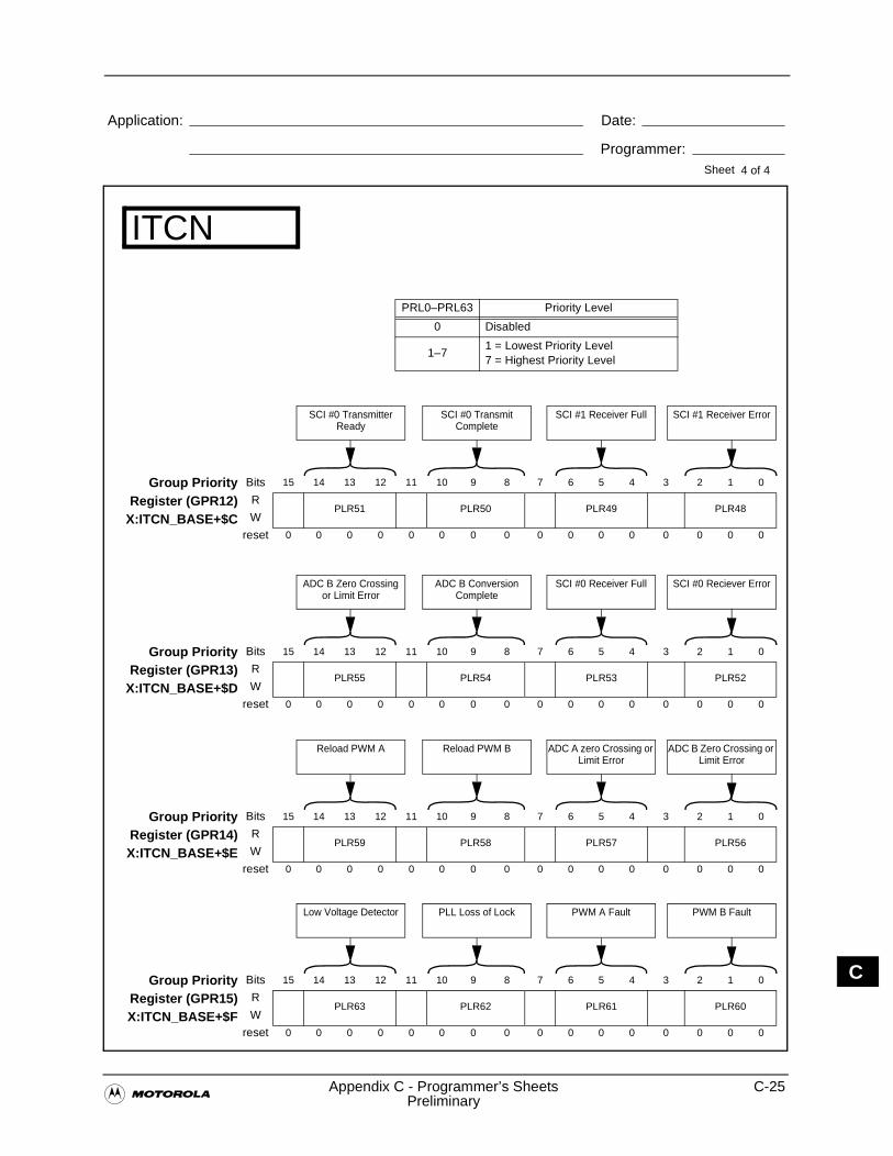
�Appendix C - Programmer’s Sheets C-25
Preliminary
Application: Date:
Programmer:Sheet
C
4 of 4
ITCN
Group PriorityRegister (GPR15)X:ITCN_BASE+$F
Bits 15 14 13 12 11 10 9 8 7 6 5 4 3 2 1 0
RPLR63 PLR62 PLR61 PLR60
W
reset 0 0 0 0 0 0 0 0 0 0 0 0 0 0 0 0
PWM B FaultPWM A FaultPLL Loss of LockLow Voltage Detector
PRL0–PRL63 Priority Level
0 Disabled
1–71 = Lowest Priority Level7 = Highest Priority Level
Group PriorityRegister (GPR12)
X:ITCN_BASE+$C
Bits 15 14 13 12 11 10 9 8 7 6 5 4 3 2 1 0
RPLR51 PLR50 PLR49 PLR48
W
reset 0 0 0 0 0 0 0 0 0 0 0 0 0 0 0 0
SCI #1 Receiver ErrorSCI #1 Receiver FullSCI #0 Transmit Complete
SCI #0 Transmitter Ready
Group PriorityRegister (GPR13)
X:ITCN_BASE+$D
Bits 15 14 13 12 11 10 9 8 7 6 5 4 3 2 1 0
RPLR55 PLR54 PLR53 PLR52
W
reset 0 0 0 0 0 0 0 0 0 0 0 0 0 0 0 0
SCI #0 Reciever ErrorSCI #0 Receiver FullADC B Conversion Complete
ADC B Zero Crossingor Limit Error
Group PriorityRegister (GPR14)X:ITCN_BASE+$E
Bits 15 14 13 12 11 10 9 8 7 6 5 4 3 2 1 0
RPLR59 PLR58 PLR57 PLR56
W
reset 0 0 0 0 0 0 0 0 0 0 0 0 0 0 0 0
ADC B Zero Crossing or Limit Error
ADC A zero Crossing or Limit Error
Reload PWM BReload PWM A
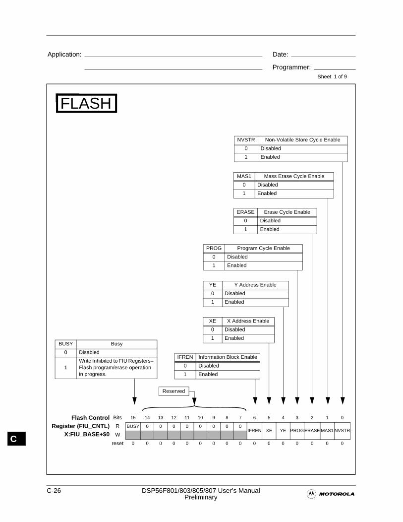
C-26 DSP56F801/803/805/807 User’s Manual�Preliminary
Application: Date:
Programmer:Sheet
C
FLASH
Flash ControlRegister (FIU_CNTL)
X:FIU_BASE+$0
Bits 15 14 13 12 11 10 9 8 7 6 5 4 3 2 1 0
R BUSY 0 0 0 0 0 0 0 0IFREN XE YE PROGERASE MAS1 NVSTR
W
reset 0 0 0 0 0 0 0 0 0 0 0 0 0 0 0 0
BUSY Busy
0 Disabled
1Write Inhibited to FIU Registers– Flash program/erase operation in progress.
IFREN Information Block Enable
0 Disabled
1 Enabled
XE X Address Enable
0 Disabled
1 Enabled
YE Y Address Enable
0 Disabled
1 Enabled
PROG Program Cycle Enable
0 Disabled
1 Enabled
ERASE Erase Cycle Enable
0 Disabled
1 Enabled
Reserved
1 of 9
MAS1 Mass Erase Cycle Enable
0 Disabled
1 Enabled
NVSTR Non-Volatile Store Cycle Enable
0 Disabled
1 Enabled
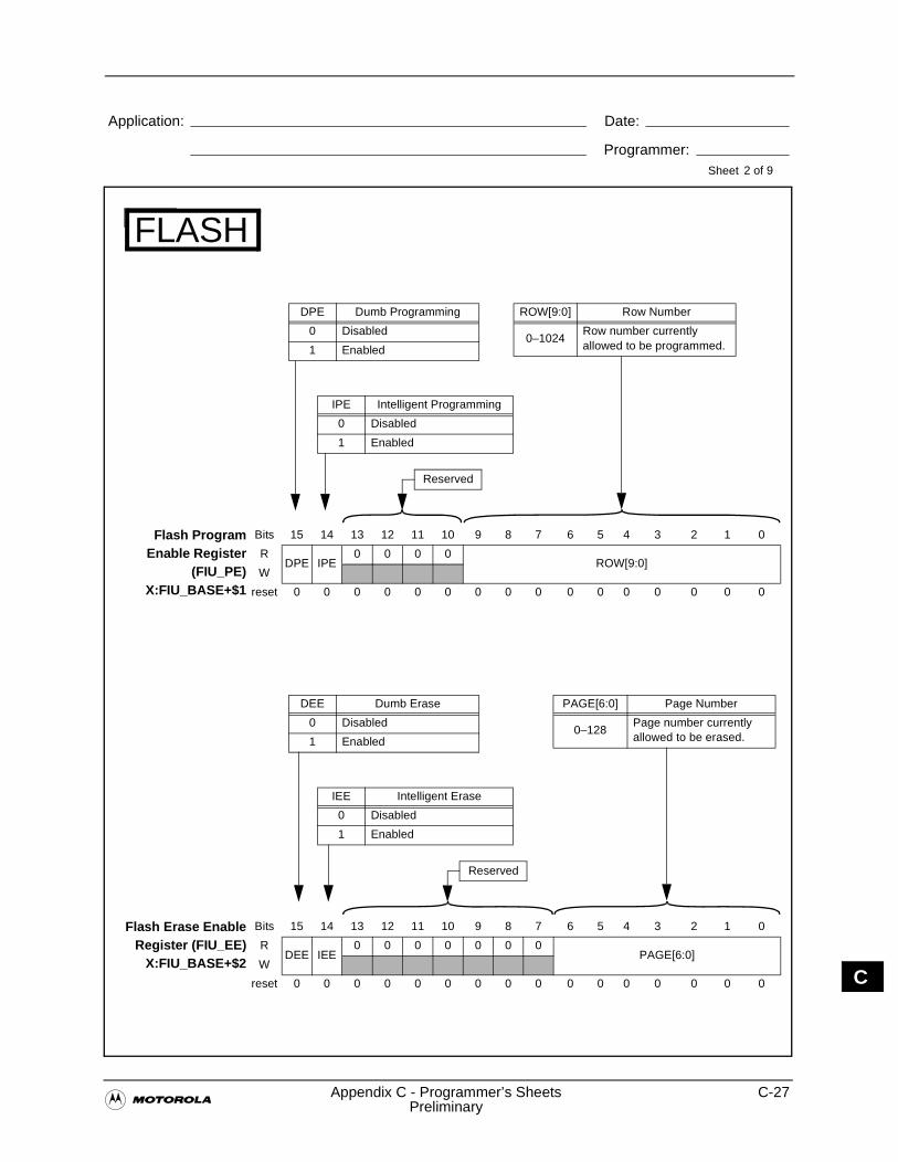
�Appendix C - Programmer’s Sheets C-27
Preliminary
Application: Date:
Programmer:Sheet
C
Flash Erase EnableRegister (FIU_EE)
X:FIU_BASE+$2
Bits 15 14 13 12 11 10 9 8 7 6 5 4 3 2 1 0
RDEE IEE
0 0 0 0 0 0 0PAGE[6:0]
W
reset 0 0 0 0 0 0 0 0 0 0 0 0 0 0 0 0
IEE Intelligent Erase
0 Disabled
1 Enabled
DEE Dumb Erase
0 Disabled
1 Enabled
PAGE[6:0] Page Number
0–128Page number currently allowed to be erased.
Reserved
2 of 9
Flash ProgramEnable Register
(FIU_PE)X:FIU_BASE+$1
Bits 15 14 13 12 11 10 9 8 7 6 5 4 3 2 1 0
RDPE IPE
0 0 0 0ROW[9:0]
W
reset 0 0 0 0 0 0 0 0 0 0 0 0 0 0 0 0
IPE Intelligent Programming
0 Disabled
1 Enabled
DPE Dumb Programming
0 Disabled
1 Enabled
ROW[9:0] Row Number
0–1024Row number currently allowed to be programmed.
Reserved
FLASH
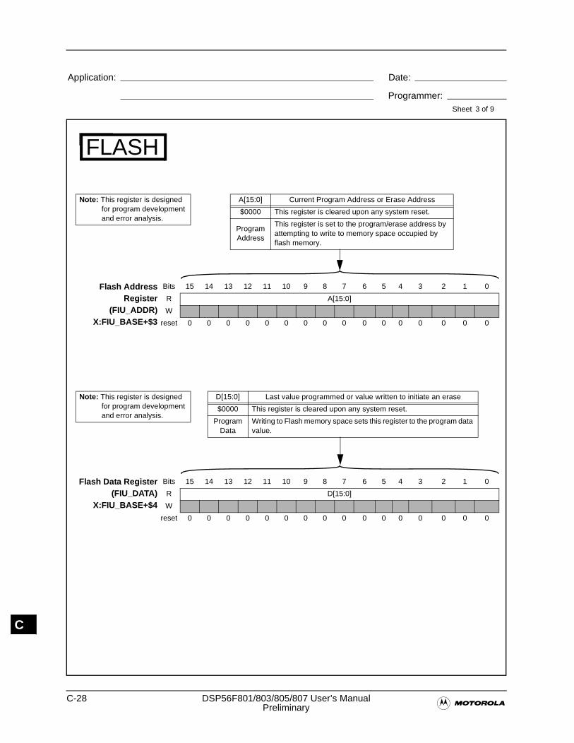
C-28 DSP56F801/803/805/807 User’s Manual�Preliminary
Application: Date:
Programmer:Sheet
C
Flash Data Register(FIU_DATA)
X:FIU_BASE+$4
Bits 15 14 13 12 11 10 9 8 7 6 5 4 3 2 1 0
R D[15:0]
W
reset 0 0 0 0 0 0 0 0 0 0 0 0 0 0 0 0
D[15:0] Last value programmed or value written to initiate an erase
$0000 This register is cleared upon any system reset.
Program Data
Writing to Flash memory space sets this register to the program data value.
Note: This register is designed for program development and error analysis.
Flash AddressRegister
(FIU_ADDR)X:FIU_BASE+$3
Bits 15 14 13 12 11 10 9 8 7 6 5 4 3 2 1 0
R A[15:0]
W
reset 0 0 0 0 0 0 0 0 0 0 0 0 0 0 0 0
A[15:0] Current Program Address or Erase Address
$0000 This register is cleared upon any system reset.
Program Address
This register is set to the program/erase address by attempting to write to memory space occupied by flash memory.
Note: This register is designed for program development and error analysis.
3 of 9
FLASH
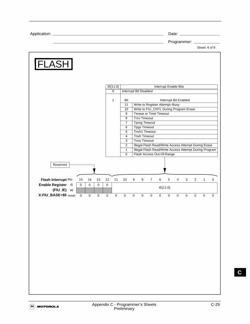
�Appendix C - Programmer’s Sheets C-29
Preliminary
Application: Date:
Programmer:Sheet
C
Flash InterruptEnable Register
(FIU_IE)X:FIU_BASE+$5
.Bits 15 14 13 12 11 10 9 8 7 6 5 4 3 2 1 0
R 0 0 0 0IE[11:0]
W
reset 0 0 0 0 0 0 0 0 0 0 0 0 0 0 0 0
Reserved
IE[11:0] Interrupt Enable Bits0 Interrupt Bit Disabled
1 Bit Interrupt Bit Enabled11 Write to Register Attempt–Busy10 Write to FIU_CNTL During Program Erase9 Terase or Tmel Timeout8 Trcv Timeout7 Tprog Timeout6 Tpgs Timeout5 Tnvh1 Timeout4 Tnvh Timeout3 Tnvs Timeout2 Illegal Flash Read/Write Access Attempt During Erase1 Illegal Flash Read/Write Access Attempt During Program0 Flash Access Out-Of-Range
4 of 9
FLASH
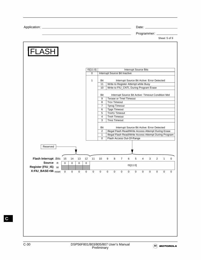
C-30 DSP56F801/803/805/807 User’s Manual�Preliminary
Application: Date:
Programmer:Sheet
C
Flash InterruptSource
Register (FIU_IS)X:FIU_BASE+$6
.Bits 15 14 13 12 11 10 9 8 7 6 5 4 3 2 1 0
R 0 0 0 0IS[11:0]
W
reset 0 0 0 0 0 0 0 0 0 0 0 0 0 0 0 0
Reserved
5 of 9
IS[11:0] Interrupt Source Bits0 Interrupt Source Bit Inactive
1 Bit Interrupt Source Bit Active: Error Detected11 Write to Register Attempt while Busy 10 Write to FIU_CNTL During Program Erase
Bit Interrupt Source Bit Active: Timeout Condition Met9 Terase or Tmel Timeout8 Trcv Timeout7 Tprog Timeout6 Tpgs Timeout5 Tnvh1 Timeout4 Tnvh Timeout3 Tnvs Timeout
Bit Interrupt Source Bit Active: Error Detected2 Illegal Flash Read/Write Access Attempt During Erase1 Illegal Flash Read/Write Access Attempt During Program0 Flash Access Out-Of-Range
FLASH
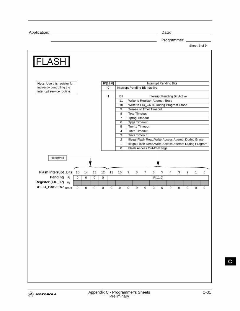
�Appendix C - Programmer’s Sheets C-31
Preliminary
Application: Date:
Programmer:Sheet
C
6 of 9
Flash InterruptPending
Register (FIU_IP)X:FIU_BASE+$7
.Bits 15 14 13 12 11 10 9 8 7 6 5 4 3 2 1 0
R 0 0 0 0 IP[11:0]
W
reset 0 0 0 0 0 0 0 0 0 0 0 0 0 0 0 0
Reserved
Note: Use this register for indirectly controlling the interrupt service routine.
IP[11:0] Interrupt Pending Bits0 Interrupt Pending Bit Inactive
1 Bit Interrupt Pending Bit Active11 Write to Register Attempt–Busy10 Write to FIU_CNTL During Program Erase9 Terase or Tmel Timeout8 Trcv Timeout7 Tprog Timeout6 Tpgs Timeout5 Tnvh1 Timeout4 Tnvh Timeout3 Tnvs Timeout2 Illegal Flash Read/Write Access Attempt During Erase1 Illegal Flash Read/Write Access Attempt During Program0 Flash Access Out-Of-Range
FLASH
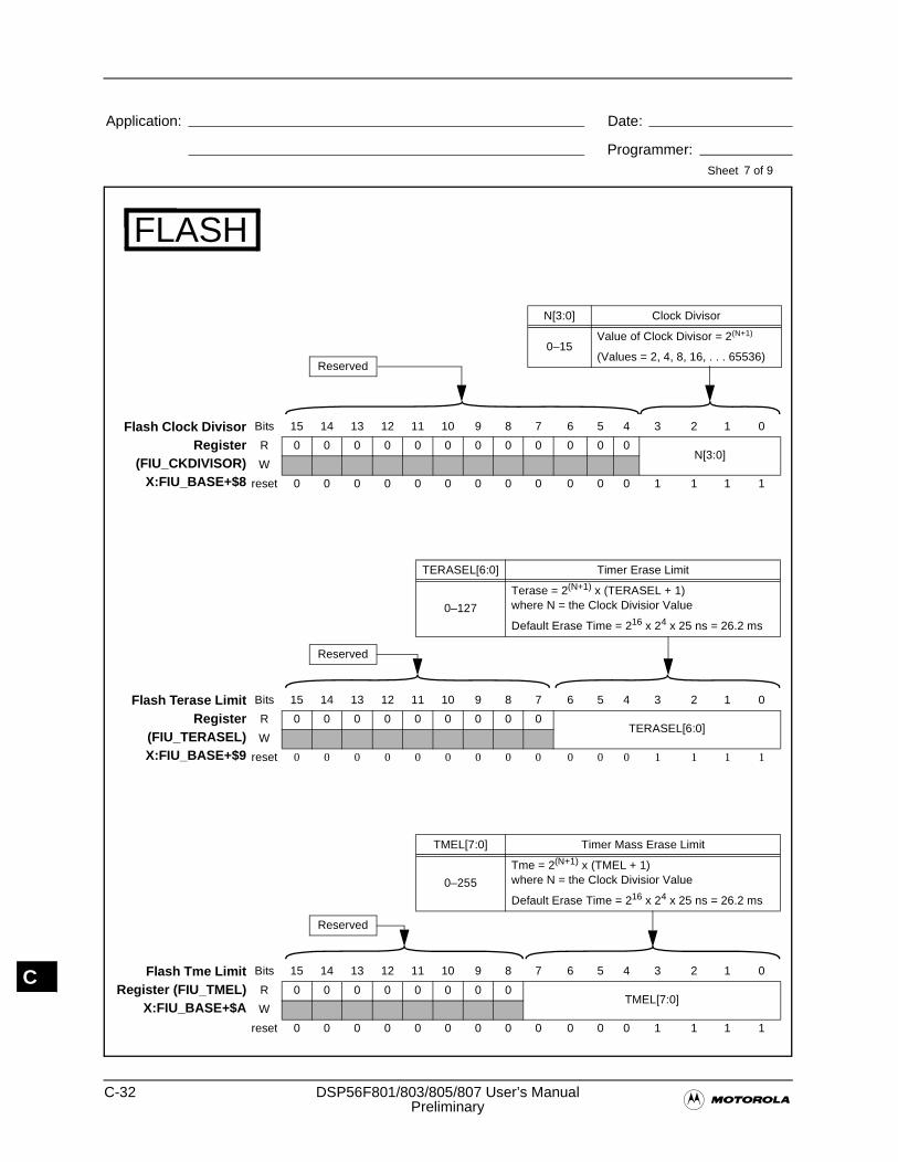
C-32 DSP56F801/803/805/807 User’s Manual�Preliminary
Application: Date:
Programmer:Sheet
C
Flash Clock DivisorRegister
(FIU_CKDIVISOR)X:FIU_BASE+$8
Bits 15 14 13 12 11 10 9 8 7 6 5 4 3 2 1 0
R 0 0 0 0 0 0 0 0 0 0 0 0N[3:0]
W
reset 0 0 0 0 0 0 0 0 0 0 0 0 1 1 1 1
N[3:0] Clock Divisor
0–15Value of Clock Divisor = 2(N+1)
(Values = 2, 4, 8, 16, . . . 65536)Reserved
7 of 9
Flash Terase LimitRegister
(FIU_TERASEL)X:FIU_BASE+$9
Bits 15 14 13 12 11 10 9 8 7 6 5 4 3 2 1 0
R 0 0 0 0 0 0 0 0 0TERASEL[6:0]
W
reset 0 0 0 0 0 0 0 0 0 0 0 0 1 1 1 1
TERASEL[6:0] Timer Erase Limit
0–127
Terase = 2(N+1) x (TERASEL + 1) where N = the Clock Divisior Value
Default Erase Time = 216 x 24 x 25 ns = 26.2 ms
Reserved
Flash Tme LimitRegister (FIU_TMEL)
X:FIU_BASE+$A
Bits 15 14 13 12 11 10 9 8 7 6 5 4 3 2 1 0
R 0 0 0 0 0 0 0 0TMEL[7:0]
W
reset 0 0 0 0 0 0 0 0 0 0 0 0 1 1 1 1
TMEL[7:0] Timer Mass Erase Limit
0–255
Tme = 2(N+1) x (TMEL + 1) where N = the Clock Divisior Value
Default Erase Time = 216 x 24 x 25 ns = 26.2 ms
Reserved
FLASH
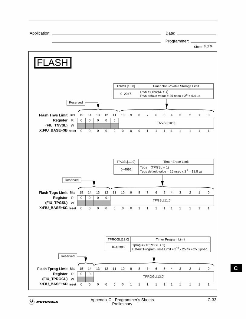
�Appendix C - Programmer’s Sheets C-33
Preliminary
Application: Date:
Programmer:Sheet
C
Flash Tpgs LimitRegister
(FIU_TPGSL)X:FIU_BASE+$C
Bits 15 14 13 12 11 10 9 8 7 6 5 4 3 2 1 0
R 0 0 0 0TPGSL[11:0]
W
reset 0 0 0 0 0 0 0 1 1 1 1 1 1 1 1 1
Reserved
8 of 9
TPGSL[11:0] Timer Erase Limit
0–4095Tpgs = (TPGSL + 1) Tpgs default value = 25 nsec x 29 = 12.8 µs
Flash Tprog LimitRegister
(FIU_TPROGL)X:FIU_BASE+$D
Bits 15 14 13 12 11 10 9 8 7 6 5 4 3 2 1 0
R 0 0TPROGL[13:0]
W
reset 0 0 0 0 0 0 1 1 1 1 1 1 1 1 1 1
TPROGL[13:0] Timer Program Limit
0–16383Tprog = (TPROGL + 1) Default Program Time Limit = 210 x 25 ns = 25.6 µsec.
Reserved
TNVSL[10:0] Timer Non-Volatile Storage Limit
0–2047Tnvs = (TNVSL + 1) Tnvs default value = 25 nsec x 28 = 6.4 µs
Flash Tnvs LimitRegister
(FIU_TNVSL)X:FIU_BASE+$B
Bits 15 14 13 12 11 10 9 8 7 6 5 4 3 2 1 0
R 0 0 0 0 0TNVSL[10:0]
W
reset 0 0 0 0 0 0 0 0 1 1 1 1 1 1 1 1
Reserved
FLASH
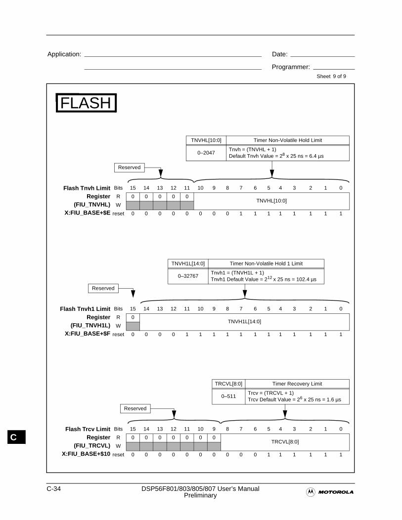
C-34 DSP56F801/803/805/807 User’s Manual�Preliminary
Application: Date:
Programmer:Sheet
C
9 of 9
Flash Tnvh LimitRegister
(FIU_TNVHL)X:FIU_BASE+$E
Bits 15 14 13 12 11 10 9 8 7 6 5 4 3 2 1 0
R 0 0 0 0 0TNVHL[10:0]
W
reset 0 0 0 0 0 0 0 0 1 1 1 1 1 1 1 1
TNVHL[10:0] Timer Non-Volatile Hold Limit
0–2047Tnvh = (TNVHL + 1) Default Tnvh Value = 28 x 25 ns = 6.4 µs
Reserved
Flash Tnvh1 LimitRegister
(FIU_TNVH1L)X:FIU_BASE+$F
Bits 15 14 13 12 11 10 9 8 7 6 5 4 3 2 1 0
R 0TNVH1L[14:0]
W
reset 0 0 0 0 1 1 1 1 1 1 1 1 1 1 1 1
TNVH1L[14:0] Timer Non-Volatile Hold 1 Limit
0–32767Tnvh1 = (TNVH1L + 1) Tnvh1 Default Value = 212 x 25 ns = 102.4 µs
Reserved
Flash Trcv LimitRegister
(FIU_TRCVL)X:FIU_BASE+$10
Bits 15 14 13 12 11 10 9 8 7 6 5 4 3 2 1 0
R 0 0 0 0 0 0 0TRCVL[8:0]
W
reset 0 0 0 0 0 0 0 0 0 0 1 1 1 1 1 1
TRCVL[8:0] Timer Recovery Limit
0–511Trcv = (TRCVL + 1) Trcv Default Value = 26 x 25 ns = 1.6 µs
Reserved
FLASH
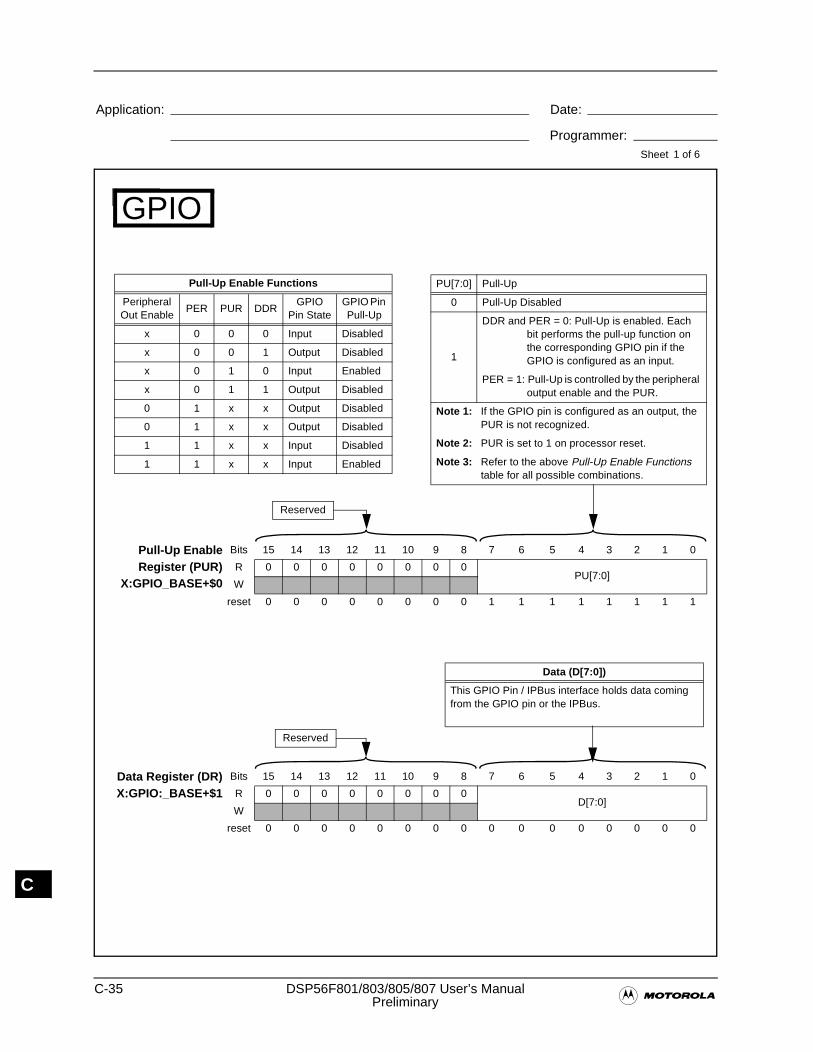
C-35 DSP56F801/803/805/807 User’s Manual�Preliminary
Application: Date:
Programmer:Sheet
C
GPIO
1 of 6
Pull-Up EnableRegister (PUR)
X:GPIO_BASE+$0
Bits 15 14 13 12 11 10 9 8 7 6 5 4 3 2 1 0
R 0 0 0 0 0 0 0 0PU[7:0]
W
reset 0 0 0 0 0 0 0 0 1 1 1 1 1 1 1 1
Pull-Up Enable Functions
Peripheral Out Enable
PER PUR DDRGPIO
Pin StateGPIO Pin Pull-Up
x 0 0 0 Input Disabled
x 0 0 1 Output Disabled
x 0 1 0 Input Enabled
x 0 1 1 Output Disabled
0 1 x x Output Disabled
0 1 x x Output Disabled
1 1 x x Input Disabled
1 1 x x Input Enabled
Reserved
Data Register (DR)X:GPIO:_BASE+$1
Bits 15 14 13 12 11 10 9 8 7 6 5 4 3 2 1 0
R 0 0 0 0 0 0 0 0D[7:0]
W
reset 0 0 0 0 0 0 0 0 0 0 0 0 0 0 0 0
Data (D[7:0])
This GPIO Pin / IPBus interface holds data coming from the GPIO pin or the IPBus.
Reserved
PU[7:0] Pull-Up
0 Pull-Up Disabled
1
DDR and PER = 0: Pull-Up is enabled. Each bit performs the pull-up function on the corresponding GPIO pin if the GPIO is configured as an input.
PER = 1: Pull-Up is controlled by the peripheral output enable and the PUR.
Note 1: If the GPIO pin is configured as an output, the PUR is not recognized.
Note 2: PUR is set to 1 on processor reset.
Note 3: Refer to the above Pull-Up Enable Functions table for all possible combinations.
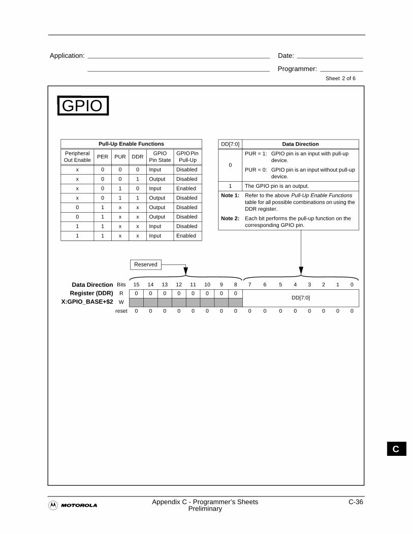
�Appendix C - Programmer’s Sheets C-36
Preliminary
Application: Date:
Programmer:Sheet
C
Data DirectionRegister (DDR)
X:GPIO_BASE+$2
Bits 15 14 13 12 11 10 9 8 7 6 5 4 3 2 1 0
R 0 0 0 0 0 0 0 0DD[7:0]
W
reset 0 0 0 0 0 0 0 0 0 0 0 0 0 0 0 0
DD[7:0] Data Direction
0
PUR = 1: GPIO pin is an input with pull-up device.
PUR = 0: GPIO pin is an input without pull-up device.
1 The GPIO pin is an output.
Note 1: Refer to the above Pull-Up Enable Functions table for all possible combinations on using the DDR register.
Note 2: Each bit performs the pull-up function on the corresponding GPIO pin.
Reserved
GPIO
2 of 6
Pull-Up Enable Functions
Peripheral Out Enable
PER PUR DDRGPIO
Pin StateGPIO Pin Pull-Up
x 0 0 0 Input Disabled
x 0 0 1 Output Disabled
x 0 1 0 Input Enabled
x 0 1 1 Output Disabled
0 1 x x Output Disabled
0 1 x x Output Disabled
1 1 x x Input Disabled
1 1 x x Input Enabled
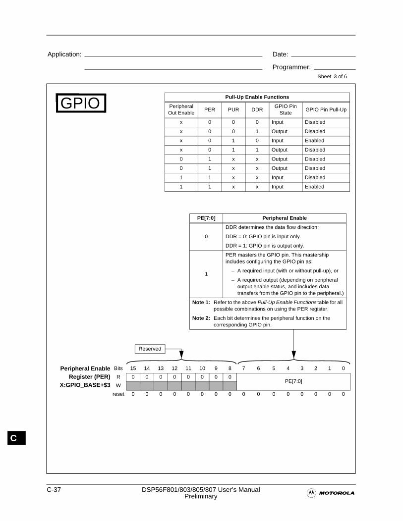
C-37 DSP56F801/803/805/807 User’s Manual�Preliminary
Application: Date:
Programmer:Sheet
C
GPIO
3 of 6
Peripheral EnableRegister (PER)
X:GPIO_BASE+$3
Bits 15 14 13 12 11 10 9 8 7 6 5 4 3 2 1 0
R 0 0 0 0 0 0 0 0PE[7:0]
W
reset 0 0 0 0 0 0 0 0 0 0 0 0 0 0 0 0
PE[7:0] Peripheral Enable
0
DDR determines the data flow direction:
DDR = 0: GPIO pin is input only.
DDR = 1: GPIO pin is output only.
1
PER masters the GPIO pin. This mastership includes configuring the GPIO pin as:
– A required input (with or without pull-up), or
– A required output (depending on peripheral output enable status, and includes data transfers from the GPIO pin to the peripheral.)
Note 1: Refer to the above Pull-Up Enable Functions table for all possible combinations on using the PER register.
Note 2: Each bit determines the peripheral function on the corresponding GPIO pin.
Reserved
Pull-Up Enable Functions
Peripheral Out Enable
PER PUR DDRGPIO Pin
StateGPIO Pin Pull-Up
x 0 0 0 Input Disabled
x 0 0 1 Output Disabled
x 0 1 0 Input Enabled
x 0 1 1 Output Disabled
0 1 x x Output Disabled
0 1 x x Output Disabled
1 1 x x Input Disabled
1 1 x x Input Enabled
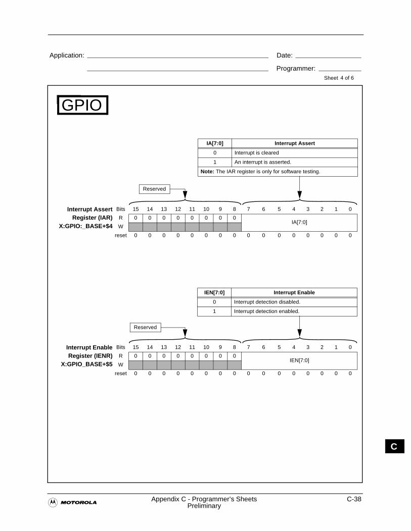
�Appendix C - Programmer’s Sheets C-38
Preliminary
Application: Date:
Programmer:Sheet
C
GPIO
4 of 6
Interrupt EnableRegister (IENR)
X:GPIO_BASE+$5
Bits 15 14 13 12 11 10 9 8 7 6 5 4 3 2 1 0
R 0 0 0 0 0 0 0 0IEN[7:0]
W
reset 0 0 0 0 0 0 0 0 0 0 0 0 0 0 0 0
IEN[7:0] Interrupt Enable
0 Interrupt detection disabled.
1 Interrupt detection enabled.
Reserved
Interrupt AssertRegister (IAR)
X:GPIO:_BASE+$4
Bits 15 14 13 12 11 10 9 8 7 6 5 4 3 2 1 0
R 0 0 0 0 0 0 0 0IA[7:0]
W
reset 0 0 0 0 0 0 0 0 0 0 0 0 0 0 0 0
IA[7:0] Interrupt Assert
0 Interrupt is cleared
1 An interrupt is asserted.
Note: The IAR register is only for software testing.
Reserved
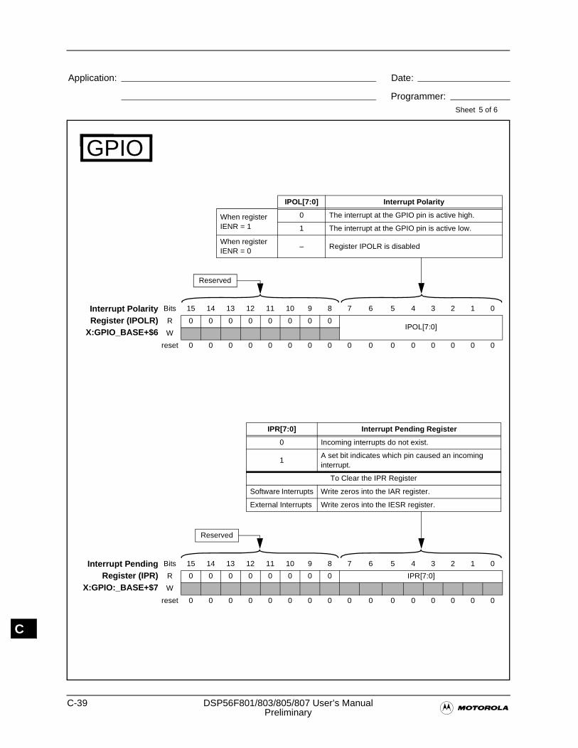
C-39 DSP56F801/803/805/807 User’s Manual�Preliminary
Application: Date:
Programmer:Sheet
C
GPIO
5 of 6
Interrupt PendingRegister (IPR)
X:GPIO:_BASE+$7
Bits 15 14 13 12 11 10 9 8 7 6 5 4 3 2 1 0
R 0 0 0 0 0 0 0 0 IPR[7:0]
W
reset 0 0 0 0 0 0 0 0 0 0 0 0 0 0 0 0
IPR[7:0] Interrupt Pending Register
0 Incoming interrupts do not exist.
1A set bit indicates which pin caused an incoming interrupt.
To Clear the IPR Register
Software Interrupts Write zeros into the IAR register.
External Interrupts Write zeros into the IESR register.
Reserved
Interrupt PolarityRegister (IPOLR)
X:GPIO_BASE+$6
Bits 15 14 13 12 11 10 9 8 7 6 5 4 3 2 1 0
R 0 0 0 0 0 0 0 0IPOL[7:0]
W
reset 0 0 0 0 0 0 0 0 0 0 0 0 0 0 0 0
IPOL[7:0] Interrupt Polarity
When register IENR = 1
0 The interrupt at the GPIO pin is active high.
1 The interrupt at the GPIO pin is active low.
When register IENR = 0
– Register IPOLR is disabled
Reserved
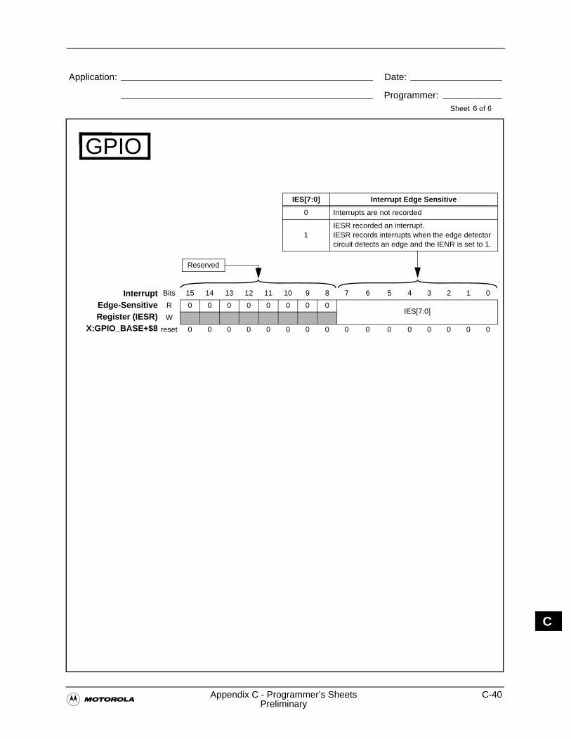
�Appendix C - Programmer’s Sheets C-40
Preliminary
Application: Date:
Programmer:Sheet
C
InterruptEdge-SensitiveRegister (IESR)
X:GPIO_BASE+$8
Bits 15 14 13 12 11 10 9 8 7 6 5 4 3 2 1 0
R 0 0 0 0 0 0 0 0IES[7:0]
W
reset 0 0 0 0 0 0 0 0 0 0 0 0 0 0 0 0
IES[7:0] Interrupt Edge Sensitive
0 Interrupts are not recorded
1IESR recorded an interrupt. IESR records interrupts when the edge detector circuit detects an edge and the IENR is set to 1.
Reserved
GPIO
6 of 6
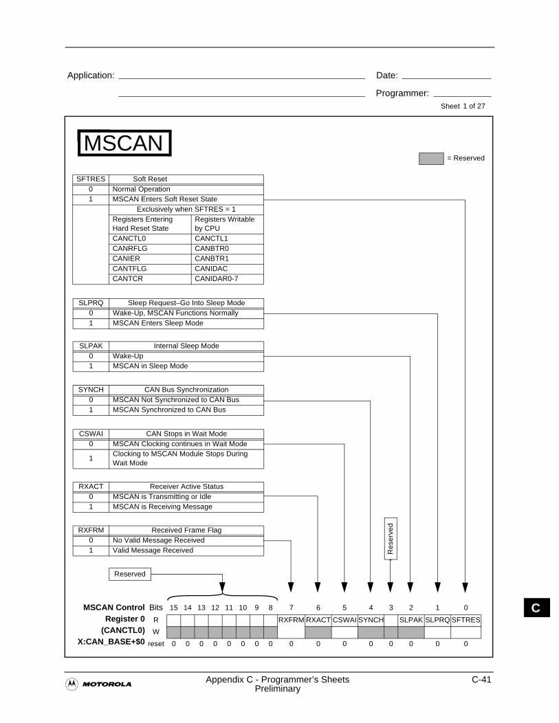
�Appendix C - Programmer’s Sheets C-41
Preliminary
Application: Date:
Programmer:Sheet
C
MSCAN
MSCAN ControlRegister 0
(CANCTL0)X:CAN_BASE+$0
Bits 15 14 13 12 11 10 9 8 7 6 5 4 3 2 1 0
R RXFRM RXACT CSWAI SYNCH SLPAK SLPRQ SFTRES
W
reset 0 0 0 0 0 0 0 0 0 0 0 0 0 0 0 0
Reserved
1 of 27
RXFRM Received Frame Flag0 No Valid Message Received 1 Valid Message Received
CSWAI CAN Stops in Wait Mode0 MSCAN Clocking continues in Wait Mode
1Clocking to MSCAN Module Stops During Wait Mode
RXACT Receiver Active Status0 MSCAN is Transmitting or Idle1 MSCAN is Receiving Message
SYNCH CAN Bus Synchronization0 MSCAN Not Synchronized to CAN Bus1 MSCAN Synchronized to CAN Bus
SLPAK Internal Sleep Mode0 Wake-Up1 MSCAN in Sleep Mode
SLPRQ Sleep Request–Go Into Sleep Mode0 Wake-Up, MSCAN Functions Normally1 MSCAN Enters Sleep Mode
SFTRES Soft Reset0 Normal Operation1 MSCAN Enters Soft Reset State
Exclusively when SFTRES = 1Registers Entering Hard Reset State
Registers Writable by CPU
CANCTL0 CANCTL1CANRFLG CANBTR0CANIER CANBTR1CANTFLG CANIDACCANTCR CANIDAR0-7
Res
erve
d
Appendix C
= Reserved
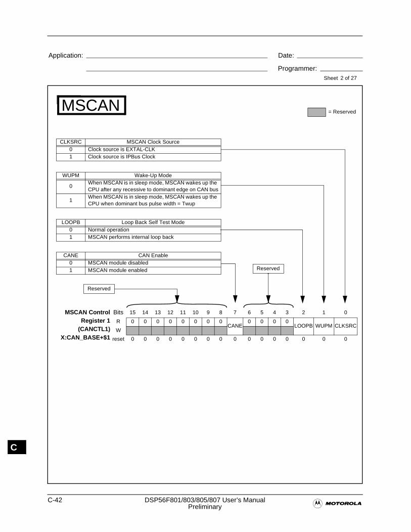
C-42 DSP56F801/803/805/807 User’s Manual�Preliminary
Application: Date:
Programmer:Sheet
C
MSCAN
MSCAN ControlRegister 1
(CANCTL1)X:CAN_BASE+$1
Bits 15 14 13 12 11 10 9 8 7 6 5 4 3 2 1 0
R 0 0 0 0 0 0 0 0CANE
0 0 0 0LOOPB WUPM CLKSRC
W
reset 0 0 0 0 0 0 0 0 0 0 0 0 0 0 0 0
Reserved
2 of 27
CANE CAN Enable0 MSCAN module disabled1 MSCAN module enabled
WUPM Wake-Up Mode
0When MSCAN is in sleep mode, MSCAN wakes up the CPU after any recessive to dominant edge on CAN bus
1When MSCAN is in sleep mode, MSCAN wakes up the CPU when dominant bus pulse width = Twup
LOOPB Loop Back Self Test Mode0 Normal operation1 MSCAN performs internal loop back
CLKSRC MSCAN Clock Source0 Clock source is EXTAL-CLK1 Clock source is IPBus Clock
Reserved
= Reserved
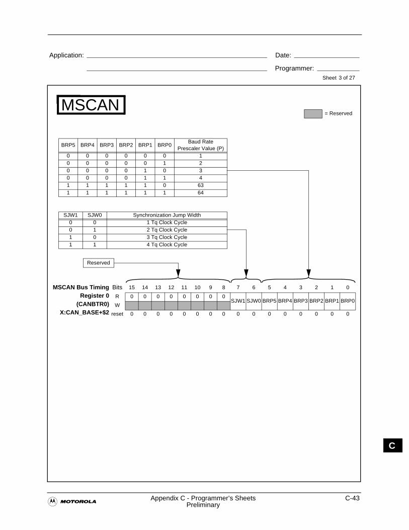
�Appendix C - Programmer’s Sheets C-43
Preliminary
Application: Date:
Programmer:Sheet
C
MSCAN
MSCAN Bus TimingRegister 0
(CANBTR0)X:CAN_BASE+$2
Bits 15 14 13 12 11 10 9 8 7 6 5 4 3 2 1 0
R 0 0 0 0 0 0 0 0SJW1 SJW0 BRP5 BRP4 BRP3 BRP2 BRP1 BRP0
W
reset 0 0 0 0 0 0 0 0 0 0 0 0 0 0 0 0
Reserved
3 of 27
SJW1 SJW0 Synchronization Jump Width0 0 1 Tq Clock Cycle0 1 2 Tq Clock Cycle1 0 3 Tq Clock Cycle1 1 4 Tq Clock Cycle
BRP5 BRP4 BRP3 BRP2 BRP1 BRP0Baud Rate
Prescaler Value (P)0 0 0 0 0 0 10 0 0 0 0 1 20 0 0 0 1 0 30 0 0 0 1 1 41 1 1 1 1 0 631 1 1 1 1 1 64
= Reserved
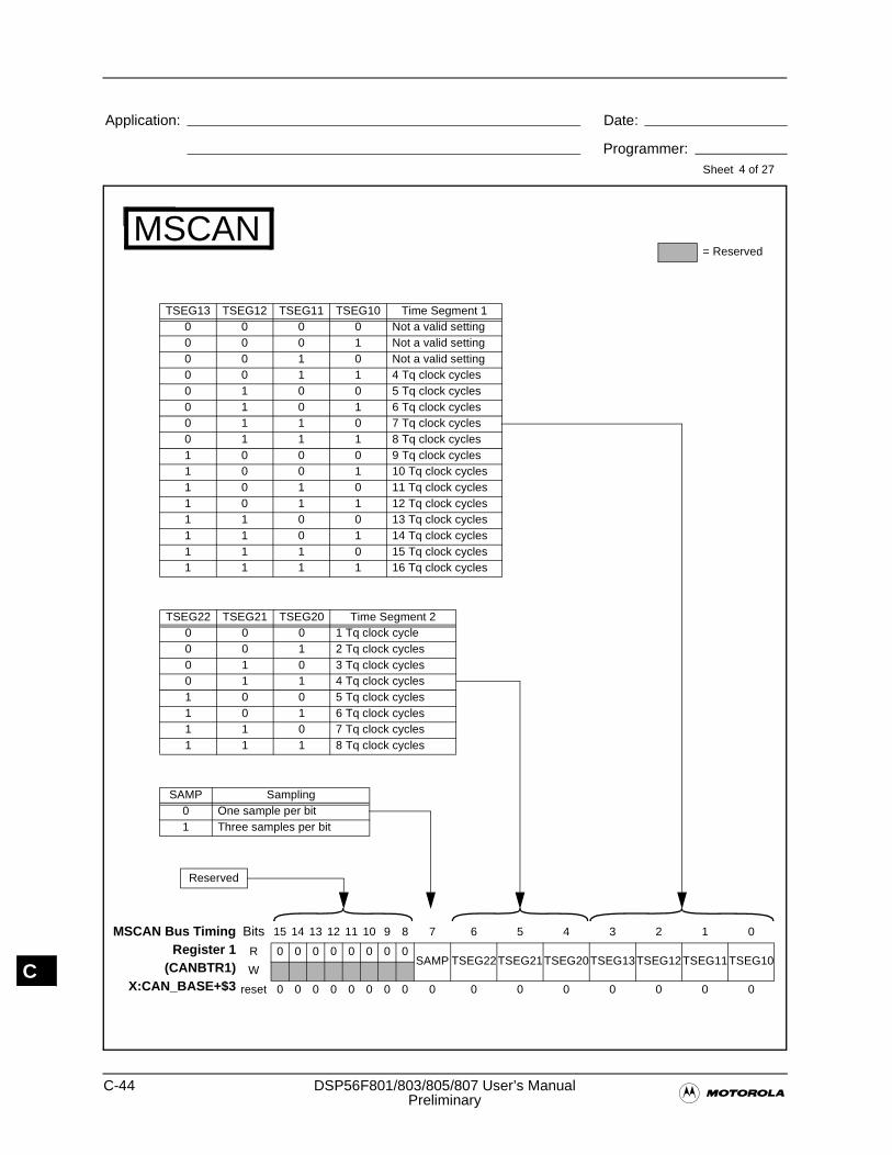
C-44 DSP56F801/803/805/807 User’s Manual�Preliminary
Application: Date:
Programmer:Sheet
C
MSCAN
MSCAN Bus TimingRegister 1
(CANBTR1)X:CAN_BASE+$3
Bits 15 14 13 12 11 10 9 8 7 6 5 4 3 2 1 0
R 0 0 0 0 0 0 0 0SAMP TSEG22TSEG21TSEG20TSEG13TSEG12TSEG11TSEG10
W
reset 0 0 0 0 0 0 0 0 0 0 0 0 0 0 0 0
Reserved
4 of 27
SAMP Sampling0 One sample per bit1 Three samples per bit
TSEG13 TSEG12 TSEG11 TSEG10 Time Segment 10 0 0 0 Not a valid setting0 0 0 1 Not a valid setting0 0 1 0 Not a valid setting0 0 1 1 4 Tq clock cycles0 1 0 0 5 Tq clock cycles0 1 0 1 6 Tq clock cycles0 1 1 0 7 Tq clock cycles0 1 1 1 8 Tq clock cycles1 0 0 0 9 Tq clock cycles1 0 0 1 10 Tq clock cycles1 0 1 0 11 Tq clock cycles1 0 1 1 12 Tq clock cycles1 1 0 0 13 Tq clock cycles1 1 0 1 14 Tq clock cycles1 1 1 0 15 Tq clock cycles1 1 1 1 16 Tq clock cycles
TSEG22 TSEG21 TSEG20 Time Segment 20 0 0 1 Tq clock cycle 0 0 1 2 Tq clock cycles0 1 0 3 Tq clock cycles0 1 1 4 Tq clock cycles1 0 0 5 Tq clock cycles1 0 1 6 Tq clock cycles1 1 0 7 Tq clock cycles1 1 1 8 Tq clock cycles
= Reserved
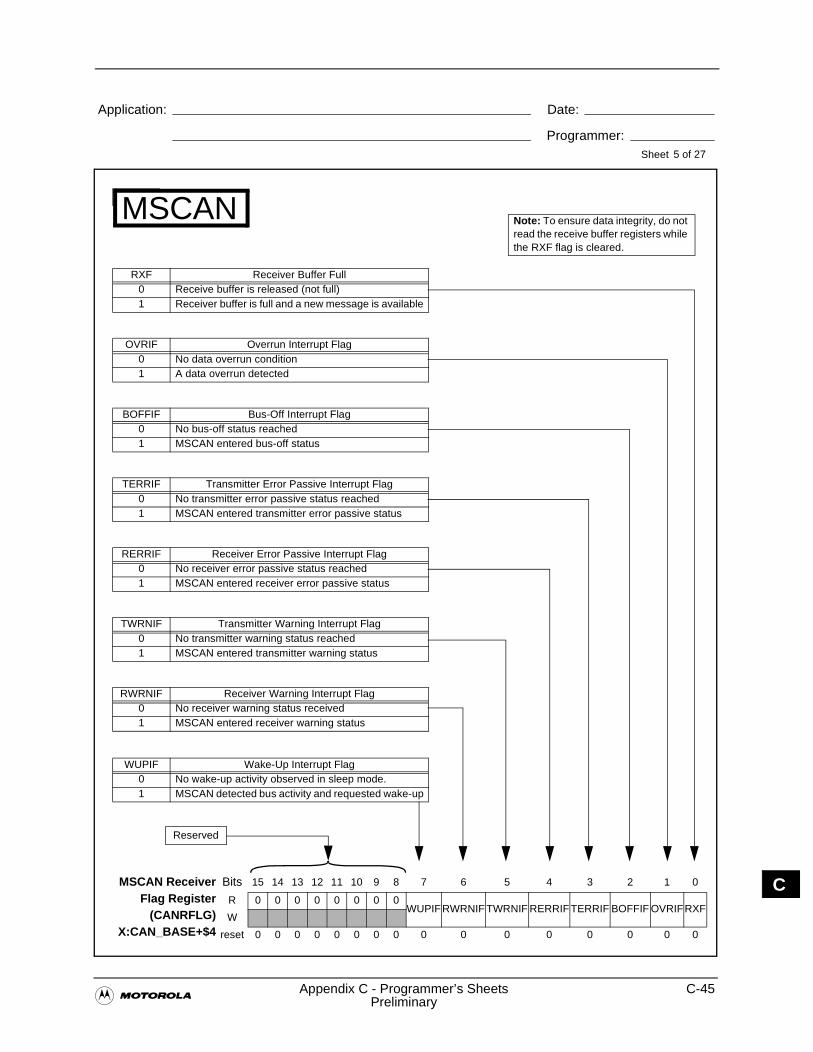
�Appendix C - Programmer’s Sheets C-45
Preliminary
Application: Date:
Programmer:Sheet
C
MSCAN
MSCAN ReceiverFlag Register
(CANRFLG)X:CAN_BASE+$4
Bits 15 14 13 12 11 10 9 8 7 6 5 4 3 2 1 0
R 0 0 0 0 0 0 0 0WUPIFRWRNIF TWRNIF RERRIF TERRIF BOFFIF OVRIFRXF
W
reset 0 0 0 0 0 0 0 0 0 0 0 0 0 0 0 0
Reserved
5 of 27
WUPIF Wake-Up Interrupt Flag0 No wake-up activity observed in sleep mode.1 MSCAN detected bus activity and requested wake-up
TWRNIF Transmitter Warning Interrupt Flag0 No transmitter warning status reached1 MSCAN entered transmitter warning status
RWRNIF Receiver Warning Interrupt Flag0 No receiver warning status received1 MSCAN entered receiver warning status
RERRIF Receiver Error Passive Interrupt Flag0 No receiver error passive status reached1 MSCAN entered receiver error passive status
TERRIF Transmitter Error Passive Interrupt Flag0 No transmitter error passive status reached1 MSCAN entered transmitter error passive status
BOFFIF Bus-Off Interrupt Flag0 No bus-off status reached1 MSCAN entered bus-off status
OVRIF Overrun Interrupt Flag0 No data overrun condition1 A data overrun detected
RXF Receiver Buffer Full0 Receive buffer is released (not full)1 Receiver buffer is full and a new message is available
Note: To ensure data integrity, do not read the receive buffer registers while the RXF flag is cleared.
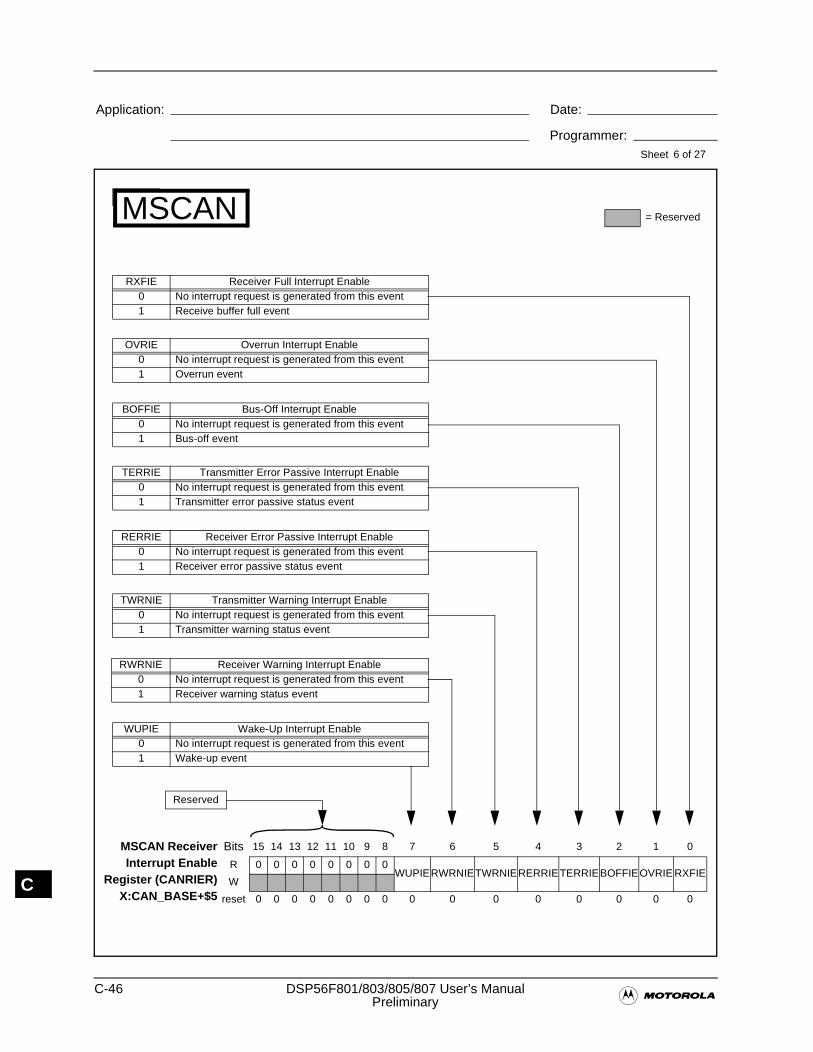
C-46 DSP56F801/803/805/807 User’s Manual�Preliminary
Application: Date:
Programmer:Sheet
C
MSCAN
MSCAN ReceiverInterrupt Enable
Register (CANRIER)X:CAN_BASE+$5
Bits 15 14 13 12 11 10 9 8 7 6 5 4 3 2 1 0
R 0 0 0 0 0 0 0 0WUPIERWRNIETWRNIERERRIETERRIEBOFFIEOVRIE RXFIE
W
reset 0 0 0 0 0 0 0 0 0 0 0 0 0 0 0 0
Reserved
6 of 27
WUPIE Wake-Up Interrupt Enable 0 No interrupt request is generated from this event1 Wake-up event
TWRNIE Transmitter Warning Interrupt Enable 0 No interrupt request is generated from this event1 Transmitter warning status event
RWRNIE Receiver Warning Interrupt Enable 0 No interrupt request is generated from this event1 Receiver warning status event
RERRIE Receiver Error Passive Interrupt Enable0 No interrupt request is generated from this event1 Receiver error passive status event
TERRIE Transmitter Error Passive Interrupt Enable0 No interrupt request is generated from this event1 Transmitter error passive status event
BOFFIE Bus-Off Interrupt Enable0 No interrupt request is generated from this event1 Bus-off event
OVRIE Overrun Interrupt Enable0 No interrupt request is generated from this event1 Overrun event
RXFIE Receiver Full Interrupt Enable0 No interrupt request is generated from this event1 Receive buffer full event
= Reserved
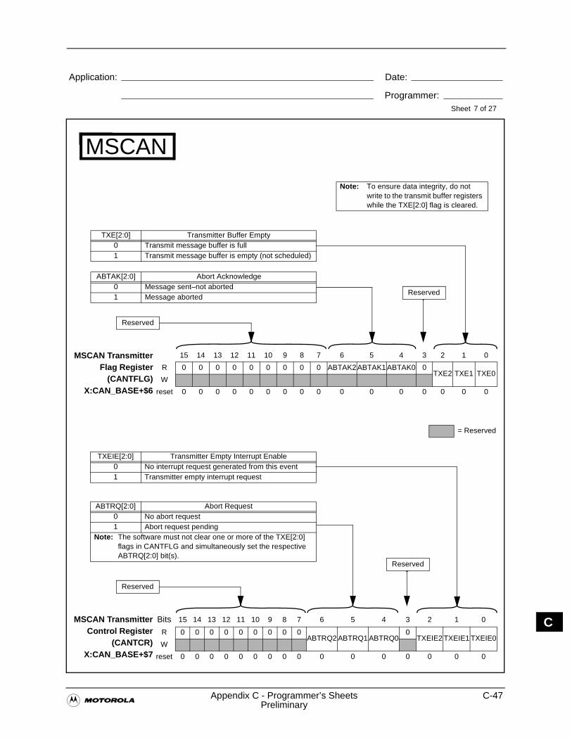
�Appendix C - Programmer’s Sheets C-47
Preliminary
Application: Date:
Programmer:Sheet
C
MSCAN
MSCAN TransmitterFlag Register
(CANTFLG)X:CAN_BASE+$6
15 14 13 12 11 10 9 8 7 6 5 4 3 2 1 0
R 0 0 0 0 0 0 0 0 0 ABTAK2 ABTAK1 ABTAK0 0TXE2 TXE1 TXE0
W
reset 0 0 0 0 0 0 0 0 0 0 0 0 0 0 0 0
Reserved
7 of 27
ABTAK[2:0] Abort Acknowledge0 Message sent–not aborted1 Message aborted
TXE[2:0] Transmitter Buffer Empty0 Transmit message buffer is full1 Transmit message buffer is empty (not scheduled)
Note: To ensure data integrity, do not write to the transmit buffer registers while the TXE[2:0] flag is cleared.
MSCAN TransmitterControl Register
(CANTCR)X:CAN_BASE+$7
Bits 15 14 13 12 11 10 9 8 7 6 5 4 3 2 1 0
R 0 0 0 0 0 0 0 0 0ABTRQ2 ABTRQ1 ABTRQ0
0TXEIE2 TXEIE1 TXEIE0
W
reset 0 0 0 0 0 0 0 0 0 0 0 0 0 0 0 0
Reserved
ABTRQ[2:0] Abort Request0 No abort request1 Abort request pending
Note: The software must not clear one or more of the TXE[2:0] flags in CANTFLG and simultaneously set the respective ABTRQ[2:0] bit(s).
TXEIE[2:0] Transmitter Empty Interrupt Enable0 No interrupt request generated from this event1 Transmitter empty interrupt request
Reserved
Reserved
= Reserved
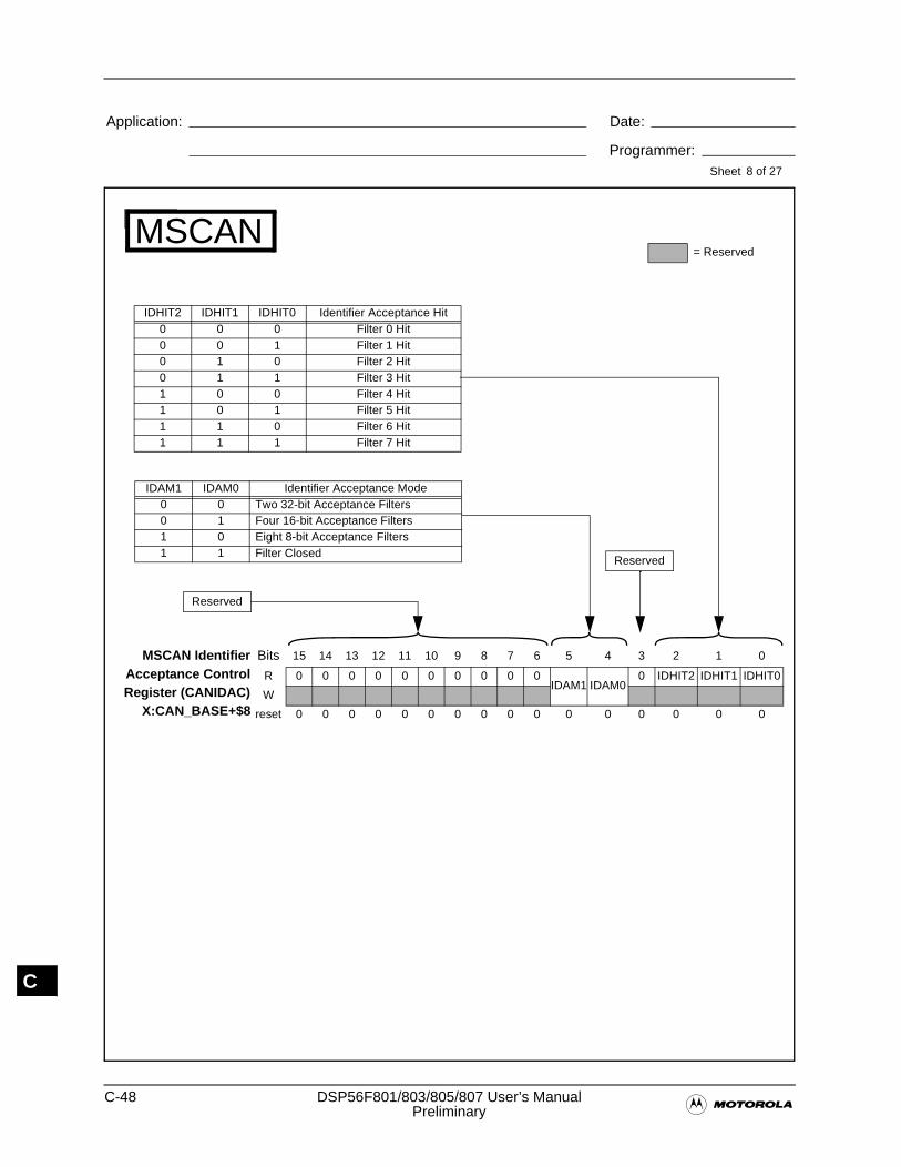
C-48 DSP56F801/803/805/807 User’s Manual�Preliminary
Application: Date:
Programmer:Sheet
C
8 of 27
MSCAN
MSCAN IdentifierAcceptance ControlRegister (CANIDAC)
X:CAN_BASE+$8
Bits 15 14 13 12 11 10 9 8 7 6 5 4 3 2 1 0
R 0 0 0 0 0 0 0 0 0 0IDAM1 IDAM0
0 IDHIT2 IDHIT1 IDHIT0
W
reset 0 0 0 0 0 0 0 0 0 0 0 0 0 0 0 0
Reserved
IDHIT2 IDHIT1 IDHIT0 Identifier Acceptance Hit0 0 0 Filter 0 Hit0 0 1 Filter 1 Hit0 1 0 Filter 2 Hit0 1 1 Filter 3 Hit1 0 0 Filter 4 Hit1 0 1 Filter 5 Hit1 1 0 Filter 6 Hit1 1 1 Filter 7 Hit
IDAM1 IDAM0 Identifier Acceptance Mode0 0 Two 32-bit Acceptance Filters0 1 Four 16-bit Acceptance Filters1 0 Eight 8-bit Acceptance Filters1 1 Filter Closed
Reserved
= Reserved
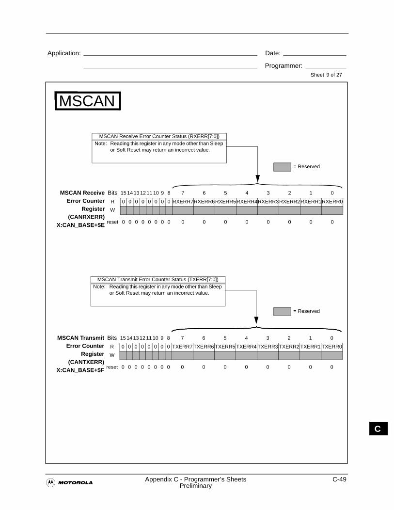
�Appendix C - Programmer’s Sheets C-49
Preliminary
Application: Date:
Programmer:Sheet
C
9 of 27
MSCAN
MSCAN ReceiveError Counter
Register(CANRXERR)
X:CAN_BASE+$E
Bits 15 14 13 12 11 10 9 8 7 6 5 4 3 2 1 0
R 0 0 0 0 0 0 0 0 RXERR7RXERR6RXERR5RXERR4RXERR3RXERR2RXERR1RXERR0
W
reset 0 0 0 0 0 0 0 0 0 0 0 0 0 0 0 0
MSCAN Receive Error Counter Status (RXERR[7:0])Note: Reading this register in any mode other than Sleep
or Soft Reset may return an incorrect value.
MSCAN TransmitError Counter
Register(CANTXERR)
X:CAN_BASE+$F
Bits 15 14 13 12 11 10 9 8 7 6 5 4 3 2 1 0
R 0 0 0 0 0 0 0 0 TXERR7 TXERR6 TXERR5 TXERR4 TXERR3 TXERR2 TXERR1 TXERR0
W
reset 0 0 0 0 0 0 0 0 0 0 0 0 0 0 0 0
MSCAN Transmit Error Counter Status (TXERR[7:0])Note: Reading this register in any mode other than Sleep
or Soft Reset may return an incorrect value.
= Reserved
= Reserved
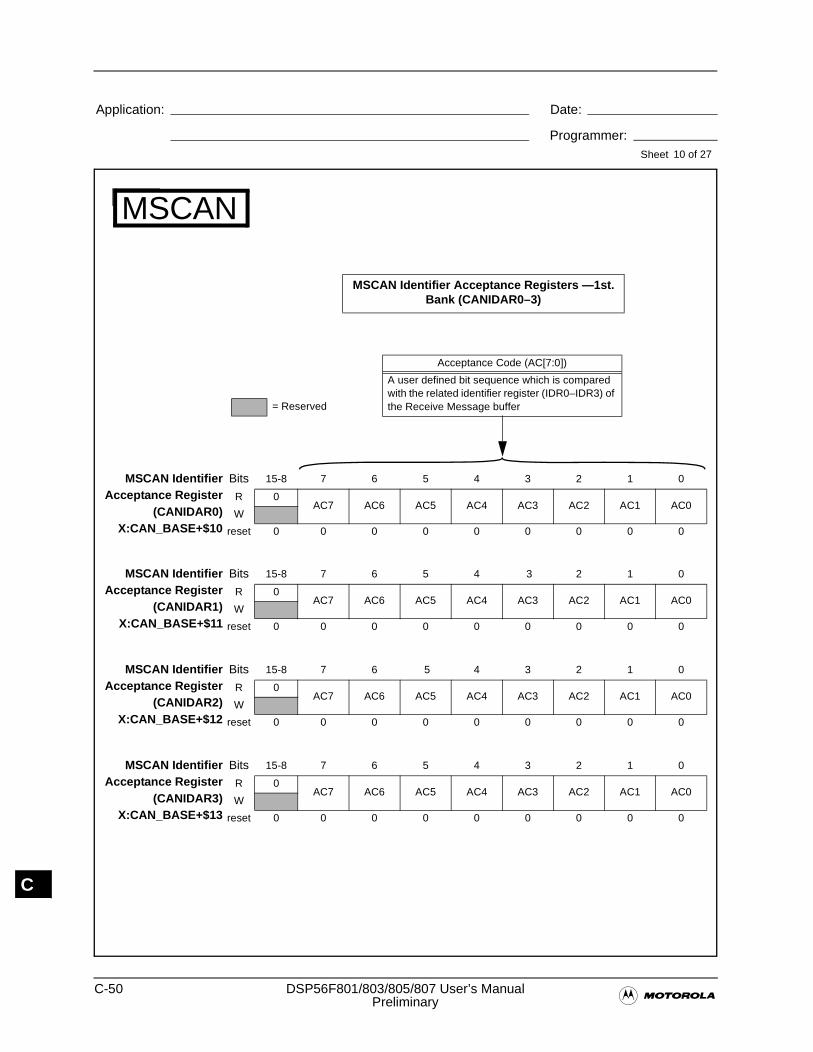
C-50 DSP56F801/803/805/807 User’s Manual�Preliminary
Application: Date:
Programmer:Sheet
C
10 of 27
MSCAN
MSCAN IdentifierAcceptance Register
(CANIDAR0)X:CAN_BASE+$10
Bits 15-8 7 6 5 4 3 2 1 0
R 0AC7 AC6 AC5 AC4 AC3 AC2 AC1 AC0
W
reset 0 0 0 0 0 0 0 0 0
Acceptance Code (AC[7:0])
A user defined bit sequence which is compared with the related identifier register (IDR0–IDR3) of the Receive Message buffer
MSCAN IdentifierAcceptance Register
(CANIDAR2)X:CAN_BASE+$12
Bits 15-8 7 6 5 4 3 2 1 0
R 0AC7 AC6 AC5 AC4 AC3 AC2 AC1 AC0
W
reset 0 0 0 0 0 0 0 0 0
MSCAN IdentifierAcceptance Register
(CANIDAR3)X:CAN_BASE+$13
Bits 15-8 7 6 5 4 3 2 1 0
R 0AC7 AC6 AC5 AC4 AC3 AC2 AC1 AC0
W
reset 0 0 0 0 0 0 0 0 0
MSCAN IdentifierAcceptance Register
(CANIDAR1)X:CAN_BASE+$11
Bits 15-8 7 6 5 4 3 2 1 0
R 0AC7 AC6 AC5 AC4 AC3 AC2 AC1 AC0
W
reset 0 0 0 0 0 0 0 0 0
= Reserved
MSCAN Identifier Acceptance Registers —1st. Bank (CANIDAR0–3)
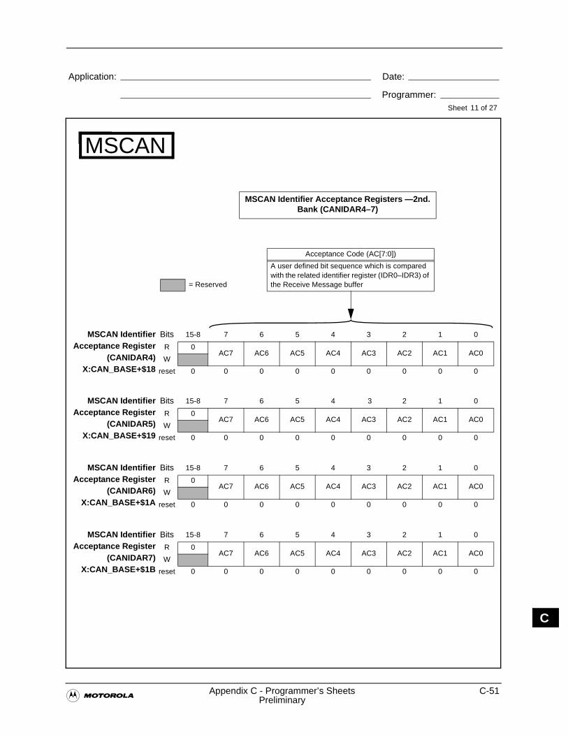
�Appendix C - Programmer’s Sheets C-51
Preliminary
Application: Date:
Programmer:Sheet
C
MSCAN
MSCAN IdentifierAcceptance Register
(CANIDAR4)X:CAN_BASE+$18
Bits 15-8 7 6 5 4 3 2 1 0
R 0AC7 AC6 AC5 AC4 AC3 AC2 AC1 AC0
W
reset 0 0 0 0 0 0 0 0 0
11 of 27
Acceptance Code (AC[7:0])
A user defined bit sequence which is compared with the related identifier register (IDR0–IDR3) of the Receive Message buffer
MSCAN IdentifierAcceptance Register
(CANIDAR5)X:CAN_BASE+$19
Bits 15-8 7 6 5 4 3 2 1 0
R 0AC7 AC6 AC5 AC4 AC3 AC2 AC1 AC0
W
reset 0 0 0 0 0 0 0 0 0
MSCAN IdentifierAcceptance Register
(CANIDAR6)X:CAN_BASE+$1A
Bits 15-8 7 6 5 4 3 2 1 0
R 0AC7 AC6 AC5 AC4 AC3 AC2 AC1 AC0
W
reset 0 0 0 0 0 0 0 0 0
MSCAN IdentifierAcceptance Register
(CANIDAR7)X:CAN_BASE+$1B
Bits 15-8 7 6 5 4 3 2 1 0
R 0AC7 AC6 AC5 AC4 AC3 AC2 AC1 AC0
W
reset 0 0 0 0 0 0 0 0 0
= Reserved
MSCAN Identifier Acceptance Registers —2nd. Bank (CANIDAR4–7)
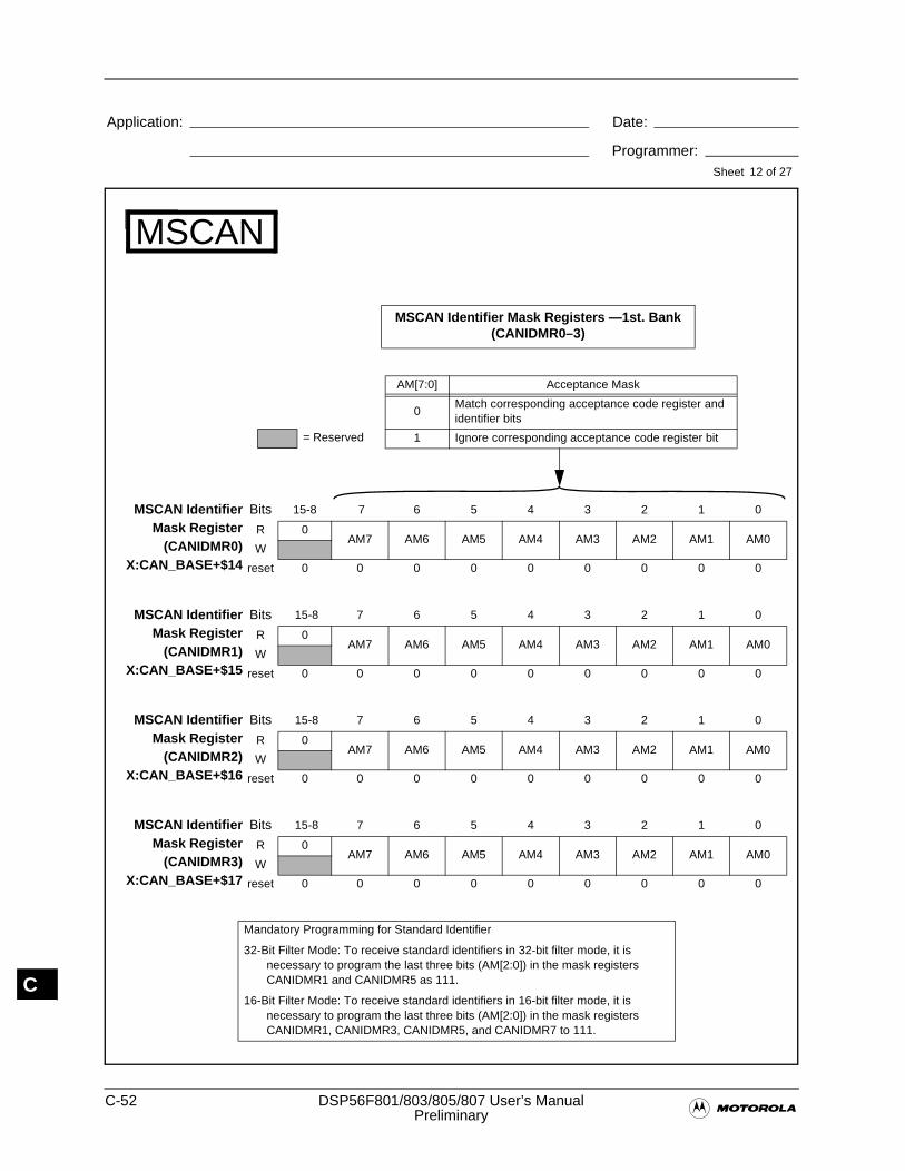
C-52 DSP56F801/803/805/807 User’s Manual�Preliminary
Application: Date:
Programmer:Sheet
C
MSCAN
MSCAN IdentifierMask Register
(CANIDMR0)X:CAN_BASE+$14
Bits 15-8 7 6 5 4 3 2 1 0
R 0AM7 AM6 AM5 AM4 AM3 AM2 AM1 AM0
W
reset 0 0 0 0 0 0 0 0 0
12 of 27
MSCAN IdentifierMask Register
(CANIDMR1)X:CAN_BASE+$15
Bits 15-8 7 6 5 4 3 2 1 0
R 0AM7 AM6 AM5 AM4 AM3 AM2 AM1 AM0
W
reset 0 0 0 0 0 0 0 0 0
MSCAN IdentifierMask Register
(CANIDMR2)X:CAN_BASE+$16
Bits 15-8 7 6 5 4 3 2 1 0
R 0AM7 AM6 AM5 AM4 AM3 AM2 AM1 AM0
W
reset 0 0 0 0 0 0 0 0 0
MSCAN IdentifierMask Register
(CANIDMR3)X:CAN_BASE+$17
Bits 15-8 7 6 5 4 3 2 1 0
R 0AM7 AM6 AM5 AM4 AM3 AM2 AM1 AM0
W
reset 0 0 0 0 0 0 0 0 0
AM[7:0] Acceptance Mask
0Match corresponding acceptance code register and identifier bits
1 Ignore corresponding acceptance code register bit
Mandatory Programming for Standard Identifier
32-Bit Filter Mode: To receive standard identifiers in 32-bit filter mode, it is necessary to program the last three bits (AM[2:0]) in the mask registers CANIDMR1 and CANIDMR5 as 111.
16-Bit Filter Mode: To receive standard identifiers in 16-bit filter mode, it is necessary to program the last three bits (AM[2:0]) in the mask registers CANIDMR1, CANIDMR3, CANIDMR5, and CANIDMR7 to 111.
= Reserved
MSCAN Identifier Mask Registers —1st. Bank (CANIDMR0–3)
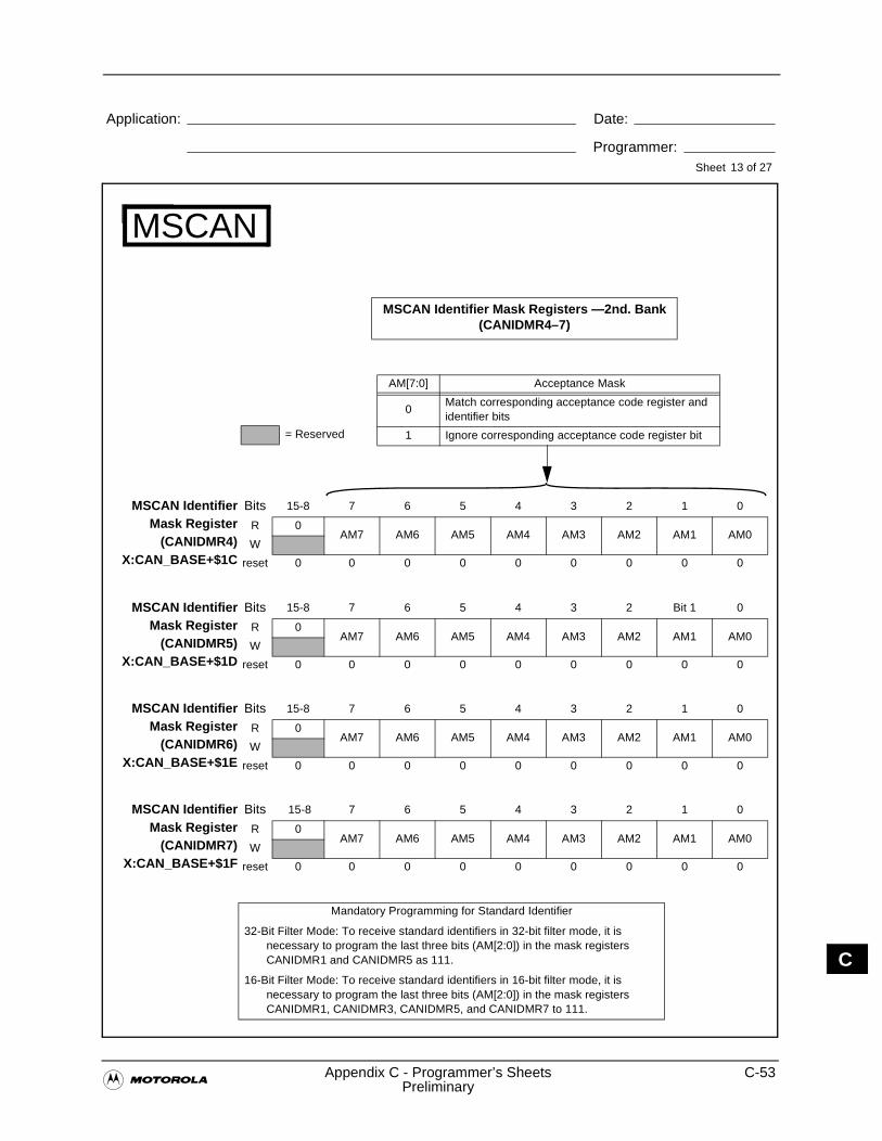
�Appendix C - Programmer’s Sheets C-53
Preliminary
Application: Date:
Programmer:Sheet
C
MSCAN
MSCAN IdentifierMask Register
(CANIDMR4)X:CAN_BASE+$1C
Bits 15-8 7 6 5 4 3 2 1 0
R 0AM7 AM6 AM5 AM4 AM3 AM2 AM1 AM0
W
reset 0 0 0 0 0 0 0 0 0
13 of 27
AM[7:0] Acceptance Mask
0Match corresponding acceptance code register and identifier bits
1 Ignore corresponding acceptance code register bit
MSCAN IdentifierMask Register
(CANIDMR5)X:CAN_BASE+$1D
Bits 15-8 7 6 5 4 3 2 Bit 1 0
R 0AM7 AM6 AM5 AM4 AM3 AM2 AM1 AM0
W
reset 0 0 0 0 0 0 0 0 0
MSCAN IdentifierMask Register
(CANIDMR6)X:CAN_BASE+$1E
Bits 15-8 7 6 5 4 3 2 1 0
R 0AM7 AM6 AM5 AM4 AM3 AM2 AM1 AM0
W
reset 0 0 0 0 0 0 0 0 0
MSCAN IdentifierMask Register
(CANIDMR7)X:CAN_BASE+$1F
Bits 15-8 7 6 5 4 3 2 1 0
R 0AM7 AM6 AM5 AM4 AM3 AM2 AM1 AM0
W
reset 0 0 0 0 0 0 0 0 0
MSCAN Identifier Mask Registers —2nd. Bank (CANIDMR4–7)
Mandatory Programming for Standard Identifier
32-Bit Filter Mode: To receive standard identifiers in 32-bit filter mode, it is necessary to program the last three bits (AM[2:0]) in the mask registers CANIDMR1 and CANIDMR5 as 111.
16-Bit Filter Mode: To receive standard identifiers in 16-bit filter mode, it is necessary to program the last three bits (AM[2:0]) in the mask registers CANIDMR1, CANIDMR3, CANIDMR5, and CANIDMR7 to 111.
= Reserved
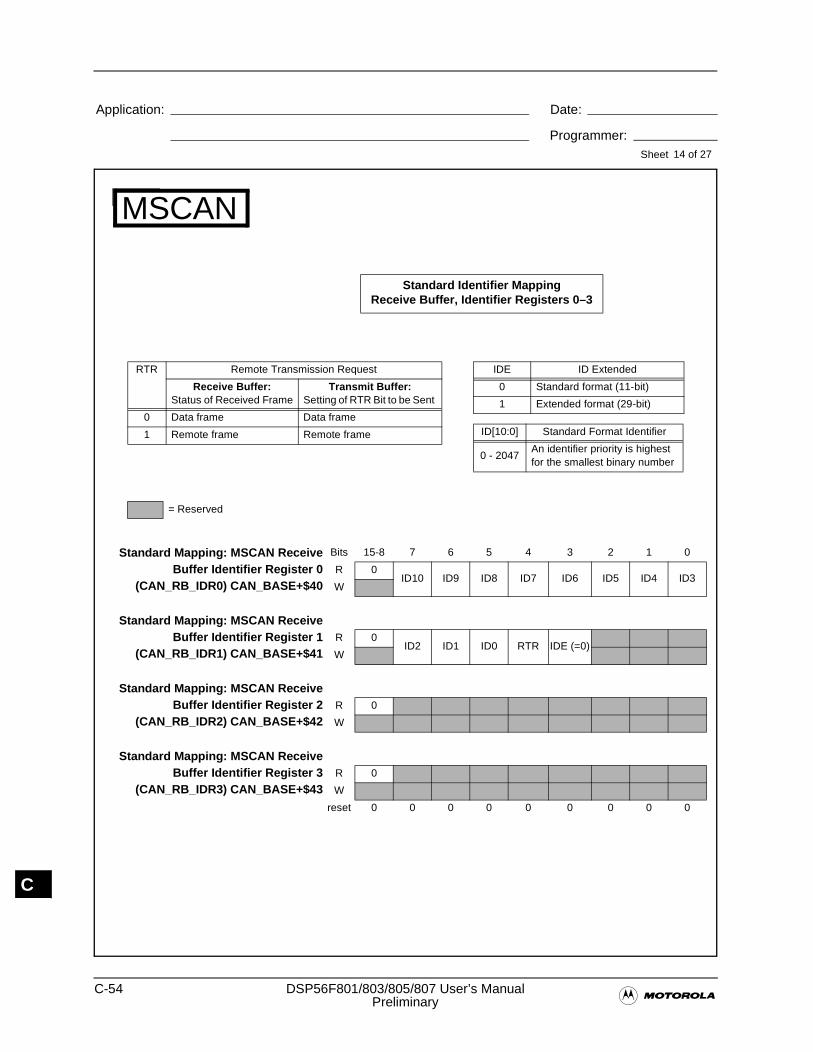
C-54 DSP56F801/803/805/807 User’s Manual�Preliminary
Application: Date:
Programmer:Sheet
C
MSCAN
14 of 27
Standard Identifier MappingReceive Buffer, Identifier Registers 0–3
Standard Mapping: MSCAN ReceiveBuffer Identifier Register 0
(CAN_RB_IDR0) CAN_BASE+$40
Bits 15-8 7 6 5 4 3 2 1 0
R 0ID10 ID9 ID8 ID7 ID6 ID5 ID4 ID3
W
Standard Mapping: MSCAN ReceiveBuffer Identifier Register 1
(CAN_RB_IDR1) CAN_BASE+$41R 0
ID2 ID1 ID0 RTR IDE (=0)W
Standard Mapping: MSCAN ReceiveBuffer Identifier Register 2
(CAN_RB_IDR2) CAN_BASE+$42R 0
W
Standard Mapping: MSCAN ReceiveBuffer Identifier Register 3
(CAN_RB_IDR3) CAN_BASE+$43R 0
W
reset 0 0 0 0 0 0 0 0 0
IDE ID Extended
0 Standard format (11-bit)
1 Extended format (29-bit)
RTR Remote Transmission Request
Receive Buffer: Status of Received Frame
Transmit Buffer: Setting of RTR Bit to be Sent
0 Data frame Data frame
1 Remote frame Remote frame ID[10:0] Standard Format Identifier
0 - 2047An identifier priority is highest for the smallest binary number
= Reserved

�Appendix C - Programmer’s Sheets C-55
Preliminary
Application: Date:
Programmer:Sheet
C
MSCAN
15 of 27
Standard Identifier MappingTransmit Buffer 0, Identifier Registers 0–3
Standard Mapping: MSCAN TransmitBuffer 0 Identifier Register 0
(CAN_TB0_IDR0) CAN_BASE+$50
Bits 15-8 7 6 5 4 3 2 1 0
R 0ID10 ID9 ID8 ID7 ID6 ID5 ID4 ID3
W
Standard Mapping: MSCAN TransmitBuffer 0 Identifier Register 1
(CAN_TB0_IDR1) CAN_BASE+$51R 0
ID2 ID1 ID0 RTR IDE (=0)W
Standard Mapping: MSCAN TransmitBuffer 0 Identifier Register 2
(CAN_TB0_IDR2) CAN_BASE+$52R 0
W
Standard Mapping: MSCAN TransmitBuffer 0 Identifier Register 3
(CAN_TB0_IDR3) CAN_BASE+$53R 0
W
reset 0 0 0 0 0 0 0 0 0
IDE ID Extended
0 Standard format (11-bit)
1 Extended format (29-bit)
RTR Remote Transmission Request
Receive Buffer: Status of Received Frame
Transmit Buffer: Setting of RTR Bit to be Sent
0 Data frame Data frame
1 Remote frame Remote frame ID[10:0] Standard Format Identifier
0 - 2047An identifier priority is highest for the smallest binary number
= Reserved
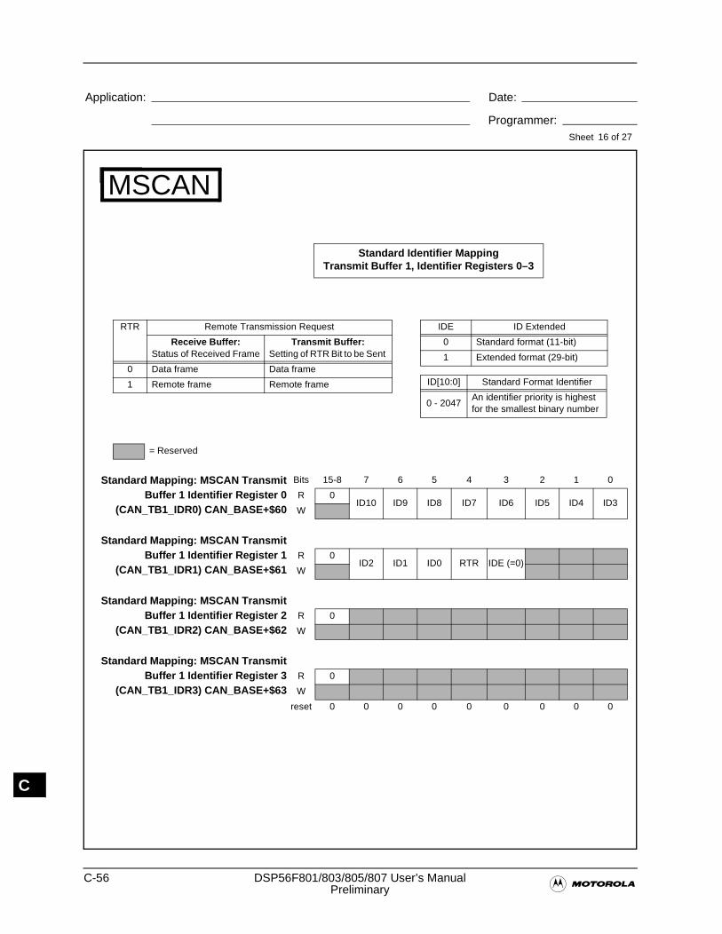
C-56 DSP56F801/803/805/807 User’s Manual�Preliminary
Application: Date:
Programmer:Sheet
C
MSCAN
16 of 27
Standard Identifier MappingTransmit Buffer 1, Identifier Registers 0–3
Standard Mapping: MSCAN TransmitBuffer 1 Identifier Register 0
(CAN_TB1_IDR0) CAN_BASE+$60
Bits 15-8 7 6 5 4 3 2 1 0
R 0ID10 ID9 ID8 ID7 ID6 ID5 ID4 ID3
W
Standard Mapping: MSCAN TransmitBuffer 1 Identifier Register 1
(CAN_TB1_IDR1) CAN_BASE+$61R 0
ID2 ID1 ID0 RTR IDE (=0)W
Standard Mapping: MSCAN TransmitBuffer 1 Identifier Register 2
(CAN_TB1_IDR2) CAN_BASE+$62R 0
W
Standard Mapping: MSCAN TransmitBuffer 1 Identifier Register 3
(CAN_TB1_IDR3) CAN_BASE+$63R 0
W
reset 0 0 0 0 0 0 0 0 0
IDE ID Extended
0 Standard format (11-bit)
1 Extended format (29-bit)
RTR Remote Transmission Request
Receive Buffer: Status of Received Frame
Transmit Buffer: Setting of RTR Bit to be Sent
0 Data frame Data frame
1 Remote frame Remote frame ID[10:0] Standard Format Identifier
0 - 2047An identifier priority is highest for the smallest binary number
= Reserved
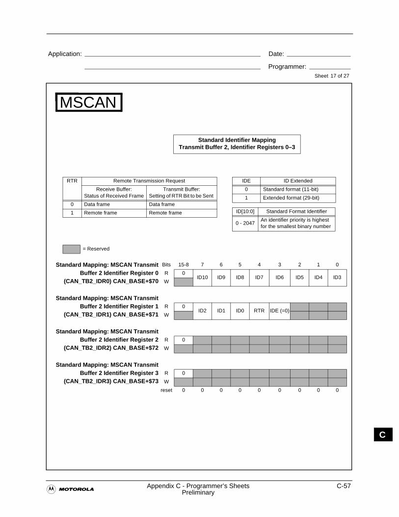
�Appendix C - Programmer’s Sheets C-57
Preliminary
Application: Date:
Programmer:Sheet
C
MSCAN
17 of 27
Standard Identifier MappingTransmit Buffer 2, Identifier Registers 0–3
Standard Mapping: MSCAN TransmitBuffer 2 Identifier Register 0
(CAN_TB2_IDR0) CAN_BASE+$70
Bits 15-8 7 6 5 4 3 2 1 0
R 0ID10 ID9 ID8 ID7 ID6 ID5 ID4 ID3
W
Standard Mapping: MSCAN TransmitBuffer 2 Identifier Register 1
(CAN_TB2_IDR1) CAN_BASE+$71R 0
ID2 ID1 ID0 RTR IDE (=0)W
Standard Mapping: MSCAN TransmitBuffer 2 Identifier Register 2
(CAN_TB2_IDR2) CAN_BASE+$72R 0
W
Standard Mapping: MSCAN TransmitBuffer 2 Identifier Register 3
(CAN_TB2_IDR3) CAN_BASE+$73R 0
W
reset 0 0 0 0 0 0 0 0 0
IDE ID Extended
0 Standard format (11-bit)
1 Extended format (29-bit)
RTR Remote Transmission Request
Receive Buffer: Status of Received Frame
Transmit Buffer: Setting of RTR Bit to be Sent
0 Data frame Data frame
1 Remote frame Remote frame ID[10:0] Standard Format Identifier
0 - 2047An identifier priority is highest for the smallest binary number
= Reserved
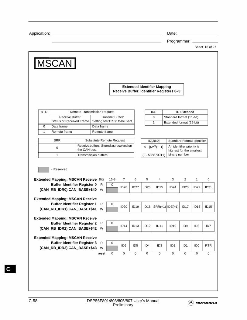
C-58 DSP56F801/803/805/807 User’s Manual�Preliminary
Application: Date:
Programmer:Sheet
C
MSCAN
18 of 27
Extended Identifier MappingReceive Buffer, Identifier Registers 0–3
Extended Mapping: MSCAN ReceiveBuffer Identifier Register 0
(CAN_RB_IDR0) CAN_BASE+$40
Bits 15-8 7 6 5 4 3 2 1 0
R 0ID28 ID27 ID26 ID25 ID24 ID23 ID22 ID21
W
Extended Mapping: MSCAN ReceiveBuffer Identifier Register 1
(CAN_RB_IDR1) CAN_BASE+$41R 0
ID20 ID19 ID18 SRR(=1) IDE(=1) ID17 ID16 ID15W
Extended Mapping: MSCAN ReceiveBuffer Identifier Register 2
(CAN_RB_IDR2) CAN_BASE+$42
R 0ID14 ID13 ID12 ID11 ID10 ID9 ID8 ID7
W
Extended Mapping: MSCAN ReceiveBuffer Identifier Register 3
(CAN_RB_IDR3) CAN_BASE+$43R 0
ID6 ID5 ID4 ID3 ID2 ID1 ID0 RTRW
reset 0 0 0 0 0 0 0 0 0
IDE ID Extended
0 Standard format (11-bit)
1 Extended format (29-bit)
RTR Remote Transmission Request
Receive Buffer: Status of Received Frame
Transmit Buffer: Setting of RTR Bit to be Sent
0 Data frame Data frame
1 Remote frame Remote frame
SRR Substitute Remote Request
0Receive buffers. Stored as received on the CAN bus.
1 Transmission buffers
ID[28:0] Standard Format Identifier
0 - {(229) – 1}
(0 - 536870911)
An identifier priority is highest for the smallest binary number
= Reserved
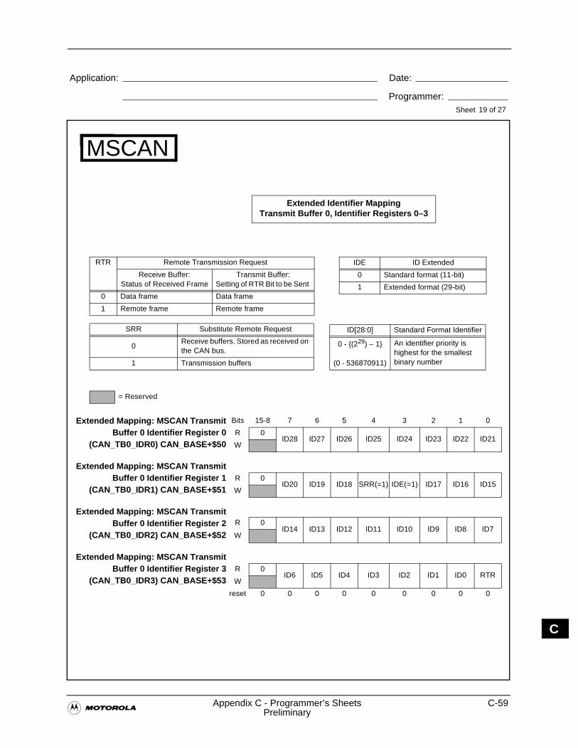
�Appendix C - Programmer’s Sheets C-59
Preliminary
Application: Date:
Programmer:Sheet
C
MSCAN
19 of 27
Extended Identifier MappingTransmit Buffer 0, Identifier Registers 0–3
Extended Mapping: MSCAN TransmitBuffer 0 Identifier Register 0
(CAN_TB0_IDR0) CAN_BASE+$50
Bits 15-8 7 6 5 4 3 2 1 0
R 0ID28 ID27 ID26 ID25 ID24 ID23 ID22 ID21
W
Extended Mapping: MSCAN TransmitBuffer 0 Identifier Register 1
(CAN_TB0_IDR1) CAN_BASE+$51R 0
ID20 ID19 ID18 SRR(=1) IDE(=1) ID17 ID16 ID15W
Extended Mapping: MSCAN TransmitBuffer 0 Identifier Register 2
(CAN_TB0_IDR2) CAN_BASE+$52
R 0ID14 ID13 ID12 ID11 ID10 ID9 ID8 ID7
W
Extended Mapping: MSCAN TransmitBuffer 0 Identifier Register 3
(CAN_TB0_IDR3) CAN_BASE+$53R 0
ID6 ID5 ID4 ID3 ID2 ID1 ID0 RTRW
reset 0 0 0 0 0 0 0 0 0
IDE ID Extended
0 Standard format (11-bit)
1 Extended format (29-bit)
RTR Remote Transmission Request
Receive Buffer: Status of Received Frame
Transmit Buffer: Setting of RTR Bit to be Sent
0 Data frame Data frame
1 Remote frame Remote frame
SRR Substitute Remote Request
0Receive buffers. Stored as received on the CAN bus.
1 Transmission buffers
ID[28:0] Standard Format Identifier
0 - {(229) – 1}
(0 - 536870911)
An identifier priority is highest for the smallest binary number
= Reserved
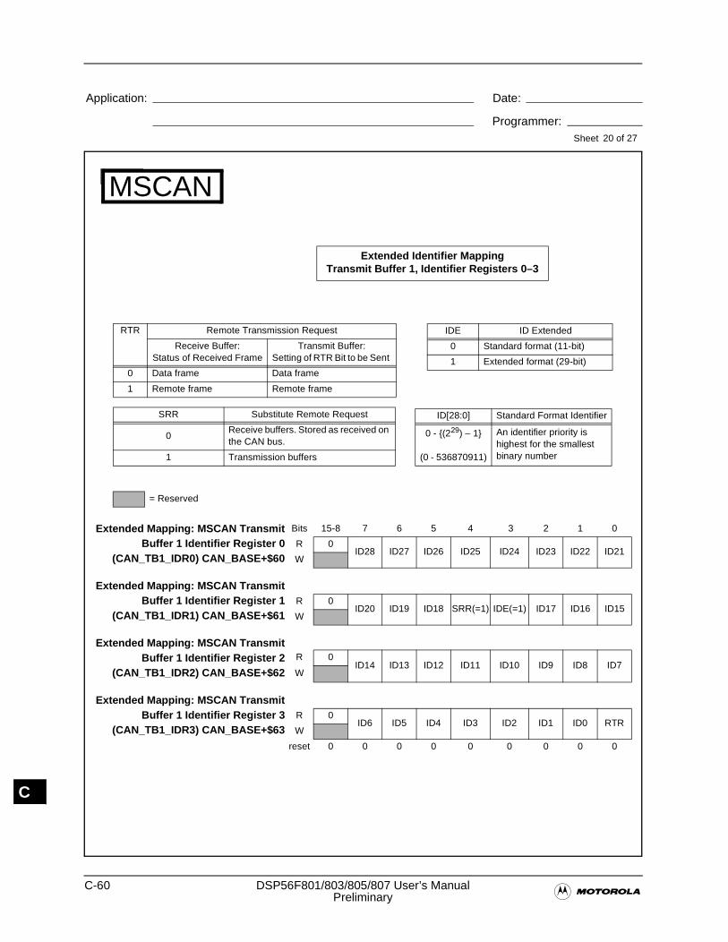
C-60 DSP56F801/803/805/807 User’s Manual�Preliminary
Application: Date:
Programmer:Sheet
C
MSCAN
20 of 27
Extended Identifier MappingTransmit Buffer 1, Identifier Registers 0–3
Extended Mapping: MSCAN TransmitBuffer 1 Identifier Register 0
(CAN_TB1_IDR0) CAN_BASE+$60
Bits 15-8 7 6 5 4 3 2 1 0
R 0ID28 ID27 ID26 ID25 ID24 ID23 ID22 ID21
W
Extended Mapping: MSCAN TransmitBuffer 1 Identifier Register 1
(CAN_TB1_IDR1) CAN_BASE+$61R 0
ID20 ID19 ID18 SRR(=1) IDE(=1) ID17 ID16 ID15W
Extended Mapping: MSCAN TransmitBuffer 1 Identifier Register 2
(CAN_TB1_IDR2) CAN_BASE+$62
R 0ID14 ID13 ID12 ID11 ID10 ID9 ID8 ID7
W
Extended Mapping: MSCAN TransmitBuffer 1 Identifier Register 3
(CAN_TB1_IDR3) CAN_BASE+$63R 0
ID6 ID5 ID4 ID3 ID2 ID1 ID0 RTRW
reset 0 0 0 0 0 0 0 0 0
IDE ID Extended
0 Standard format (11-bit)
1 Extended format (29-bit)
RTR Remote Transmission Request
Receive Buffer: Status of Received Frame
Transmit Buffer: Setting of RTR Bit to be Sent
0 Data frame Data frame
1 Remote frame Remote frame
SRR Substitute Remote Request
0Receive buffers. Stored as received on the CAN bus.
1 Transmission buffers
ID[28:0] Standard Format Identifier
0 - {(229) – 1}
(0 - 536870911)
An identifier priority is highest for the smallest binary number
= Reserved
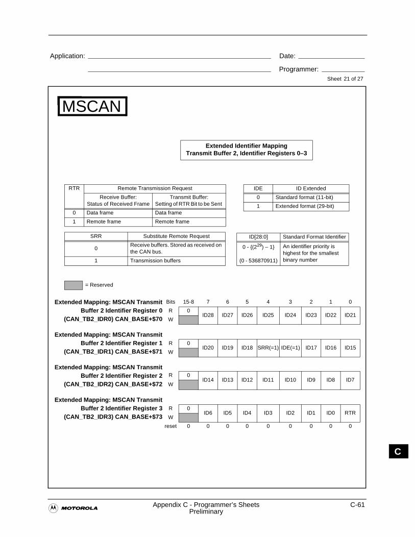
�Appendix C - Programmer’s Sheets C-61
Preliminary
Application: Date:
Programmer:Sheet
C
MSCAN
21 of 27
Extended Identifier MappingTransmit Buffer 2, Identifier Registers 0–3
Extended Mapping: MSCAN TransmitBuffer 2 Identifier Register 0
(CAN_TB2_IDR0) CAN_BASE+$70
Bits 15-8 7 6 5 4 3 2 1 0
R 0ID28 ID27 ID26 ID25 ID24 ID23 ID22 ID21
W
Extended Mapping: MSCAN TransmitBuffer 2 Identifier Register 1
(CAN_TB2_IDR1) CAN_BASE+$71R 0
ID20 ID19 ID18 SRR(=1) IDE(=1) ID17 ID16 ID15W
Extended Mapping: MSCAN TransmitBuffer 2 Identifier Register 2
(CAN_TB2_IDR2) CAN_BASE+$72
R 0ID14 ID13 ID12 ID11 ID10 ID9 ID8 ID7
W
Extended Mapping: MSCAN TransmitBuffer 2 Identifier Register 3
(CAN_TB2_IDR3) CAN_BASE+$73R 0
ID6 ID5 ID4 ID3 ID2 ID1 ID0 RTRW
reset 0 0 0 0 0 0 0 0 0
IDE ID Extended
0 Standard format (11-bit)
1 Extended format (29-bit)
RTR Remote Transmission Request
Receive Buffer: Status of Received Frame
Transmit Buffer: Setting of RTR Bit to be Sent
0 Data frame Data frame
1 Remote frame Remote frame
SRR Substitute Remote Request
0Receive buffers. Stored as received on the CAN bus.
1 Transmission buffers
ID[28:0] Standard Format Identifier
0 - {(229) – 1}
(0 - 536870911)
An identifier priority is highest for the smallest binary number
= Reserved
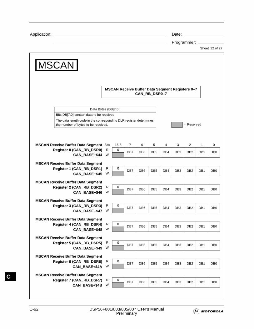
C-62 DSP56F801/803/805/807 User’s Manual�Preliminary
Application: Date:
Programmer:Sheet
C
MSCAN
22 of 27
MSCAN Receive Buffer Data Segment Registers 0–7 CAN_RB_DSR0–7
MSCAN Receive Buffer Data SegmentRegister 0 (CAN_RB_DSR0)
CAN_BASE+$44
Bits 15-8 7 6 5 4 3 2 1 0
R 0DB7 DB6 DB5 DB4 DB3 DB2 DB1 DB0
W
MSCAN Receive Buffer Data SegmentRegister 1 (CAN_RB_DSR1)
CAN_BASE+$45
R 0DB7 DB6 DB5 DB4 DB3 DB2 DB1 DB0
W
MSCAN Receive Buffer Data SegmentRegister 2 (CAN_RB_DSR2)
CAN_BASE+$46
R 0DB7 DB6 DB5 DB4 DB3 DB2 DB1 DB0
W
MSCAN Receive Buffer Data SegmentRegister 3 (CAN_RB_DSR3)
CAN_BASE+$47
R 0DB7 DB6 DB5 DB4 DB3 DB2 DB1 DB0
W
MSCAN Receive Buffer Data SegmentRegister 4 (CAN_RB_DSR4)
CAN_BASE+$48
R 0DB7 DB6 DB5 DB4 DB3 DB2 DB1 DB0
W
MSCAN Receive Buffer Data SegmentRegister 5 (CAN_RB_DSR5)
CAN_BASE+$49
R 0DB7 DB6 DB5 DB4 DB3 DB2 DB1 DB0
W
MSCAN Receive Buffer Data SegmentRegister 6 (CAN_RB_DSR6)
CAN_BASE+$4A
R 0DB7 DB6 DB5 DB4 DB3 DB2 DB1 DB0
W
MSCAN Receive Buffer Data SegmentRegister 7 (CAN_RB_DSR7)
CAN_BASE+$4B
R 0DB7 DB6 DB5 DB4 DB3 DB2 DB1 DB0
W
Data Bytes (DB[7:0])
Bits DB[7:0] contain data to be received.
The data length code in the corresponding DLR register determines the number of bytes to be received. = Reserved
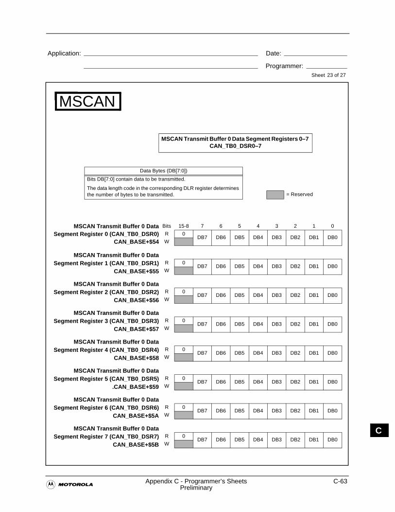
�Appendix C - Programmer’s Sheets C-63
Preliminary
Application: Date:
Programmer:Sheet
C
MSCAN
23 of 27
MSCAN Transmit Buffer 0 Data Segment Registers 0–7 CAN_TB0_DSR0–7
Data Bytes (DB[7:0])
Bits DB[7:0] contain data to be transmitted.
The data length code in the corresponding DLR register determines the number of bytes to be transmitted.
MSCAN Transmit Buffer 0 DataSegment Register 0 (CAN_TB0_DSR0)
CAN_BASE+$54
Bits 15-8 7 6 5 4 3 2 1 0
R 0DB7 DB6 DB5 DB4 DB3 DB2 DB1 DB0
W
MSCAN Transmit Buffer 0 DataSegment Register 1 (CAN_TB0_DSR1)
CAN_BASE+$55
R 0DB7 DB6 DB5 DB4 DB3 DB2 DB1 DB0
W
MSCAN Transmit Buffer 0 DataSegment Register 2 (CAN_TB0_DSR2)
CAN_BASE+$56
R 0DB7 DB6 DB5 DB4 DB3 DB2 DB1 DB0
W
MSCAN Transmit Buffer 0 DataSegment Register 3 (CAN_TB0_DSR3)
CAN_BASE+$57
R 0DB7 DB6 DB5 DB4 DB3 DB2 DB1 DB0
W
MSCAN Transmit Buffer 0 DataSegment Register 4 (CAN_TB0_DSR4)
CAN_BASE+$58
R 0DB7 DB6 DB5 DB4 DB3 DB2 DB1 DB0
W
MSCAN Transmit Buffer 0 DataSegment Register 5 (CAN_TB0_DSR5)
.CAN_BASE+$59
R 0DB7 DB6 DB5 DB4 DB3 DB2 DB1 DB0
W
MSCAN Transmit Buffer 0 DataSegment Register 6 (CAN_TB0_DSR6)
CAN_BASE+$5A
R 0DB7 DB6 DB5 DB4 DB3 DB2 DB1 DB0
W
MSCAN Transmit Buffer 0 DataSegment Register 7 (CAN_TB0_DSR7)
CAN_BASE+$5B
R 0DB7 DB6 DB5 DB4 DB3 DB2 DB1 DB0
W
= Reserved

C-64 DSP56F801/803/805/807 User’s Manual�Preliminary
Application: Date:
Programmer:Sheet
C
MSCAN
24 of 27
MSCAN Transmit Buffer 1 Data Segment Registers 0–7CAN_TB1_DSR0–7
MSCAN Transmit Buffer 1 DataSegment Register 0 (CAN_TB1_DSR0)
CAN_BASE+$64
Bits 15-8 7 6 5 4 3 2 1 0
R 0DB7 DB6 DB5 DB4 DB3 DB2 DB1 DB0
W
MSCAN Transmit Buffer 1 DataSegment Register 1 (CAN_TB1_DSR1)
CAN_BASE+$65
R 0DB7 DB6 DB5 DB4 DB3 DB2 DB1 DB0
W
MSCAN Transmit Buffer 1 DataSegment Register 2 (CAN_TB1_DSR2)
CAN_BASE+$66
R 0DB7 DB6 DB5 DB4 DB3 DB2 DB1 DB0
W
MSCAN Transmit Buffer 1 DataSegment Register 3 (CAN_TB1_DSR3)
CAN_BASE+$67
R 0DB7 DB6 DB5 DB4 DB3 DB2 DB1 DB0
W
MSCAN Transmit Buffer 1 DataSegment Register 4 (CAN_TB1_DSR4)
CAN_BASE+$68
R 0DB7 DB6 DB5 DB4 DB3 DB2 DB1 DB0
W
MSCAN Transmit Buffer 1 DataSegment Register 5 (CAN_TB1_DSR5)
CAN_BASE+$69
R 0DB7 DB6 DB5 DB4 DB3 DB2 DB1 DB0
W
MSCAN Transmit Buffer 1 DataSegment Register 6 (CAN_TB1_DSR6)
CAN_BASE+$6A
R 0DB7 DB6 DB5 DB4 DB3 DB2 DB1 DB0
W
MSCAN Transmit Buffer 1 DataSegment Register 7 (CAN_TB1_DSR7)
CAN_BASE+$6B
R 0DB7 DB6 DB5 DB4 DB3 DB2 DB1 DB0
W
Data Bytes (DB[7:0])
Bits DB[7:0] contain data to be transmitted.
The data length code in the corresponding DLR register determines the number of bytes to be transmitted. = Reserved
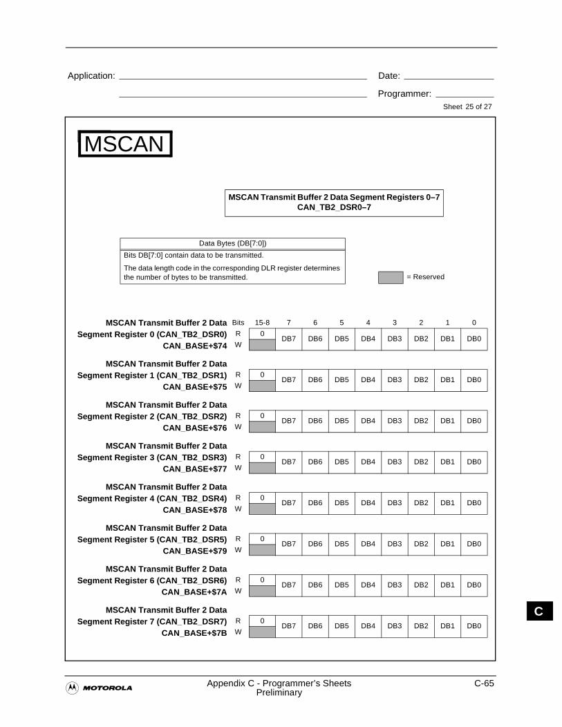
�Appendix C - Programmer’s Sheets C-65
Preliminary
Application: Date:
Programmer:Sheet
C
MSCAN
25 of 27
MSCAN Transmit Buffer 2 Data Segment Registers 0–7CAN_TB2_DSR0–7
Data Bytes (DB[7:0])
Bits DB[7:0] contain data to be transmitted.
The data length code in the corresponding DLR register determines the number of bytes to be transmitted. = Reserved
MSCAN Transmit Buffer 2 DataSegment Register 0 (CAN_TB2_DSR0)
CAN_BASE+$74
Bits 15-8 7 6 5 4 3 2 1 0
R 0DB7 DB6 DB5 DB4 DB3 DB2 DB1 DB0
W
MSCAN Transmit Buffer 2 DataSegment Register 1 (CAN_TB2_DSR1)
CAN_BASE+$75
R 0DB7 DB6 DB5 DB4 DB3 DB2 DB1 DB0
W
MSCAN Transmit Buffer 2 DataSegment Register 2 (CAN_TB2_DSR2)
CAN_BASE+$76
R 0DB7 DB6 DB5 DB4 DB3 DB2 DB1 DB0
W
MSCAN Transmit Buffer 2 DataSegment Register 3 (CAN_TB2_DSR3)
CAN_BASE+$77
R 0DB7 DB6 DB5 DB4 DB3 DB2 DB1 DB0
W
MSCAN Transmit Buffer 2 DataSegment Register 4 (CAN_TB2_DSR4)
CAN_BASE+$78
R 0DB7 DB6 DB5 DB4 DB3 DB2 DB1 DB0
W
MSCAN Transmit Buffer 2 DataSegment Register 5 (CAN_TB2_DSR5)
CAN_BASE+$79
R 0DB7 DB6 DB5 DB4 DB3 DB2 DB1 DB0
W
MSCAN Transmit Buffer 2 DataSegment Register 6 (CAN_TB2_DSR6)
CAN_BASE+$7A
R 0DB7 DB6 DB5 DB4 DB3 DB2 DB1 DB0
W
MSCAN Transmit Buffer 2 DataSegment Register 7 (CAN_TB2_DSR7)
CAN_BASE+$7B
R 0DB7 DB6 DB5 DB4 DB3 DB2 DB1 DB0
W
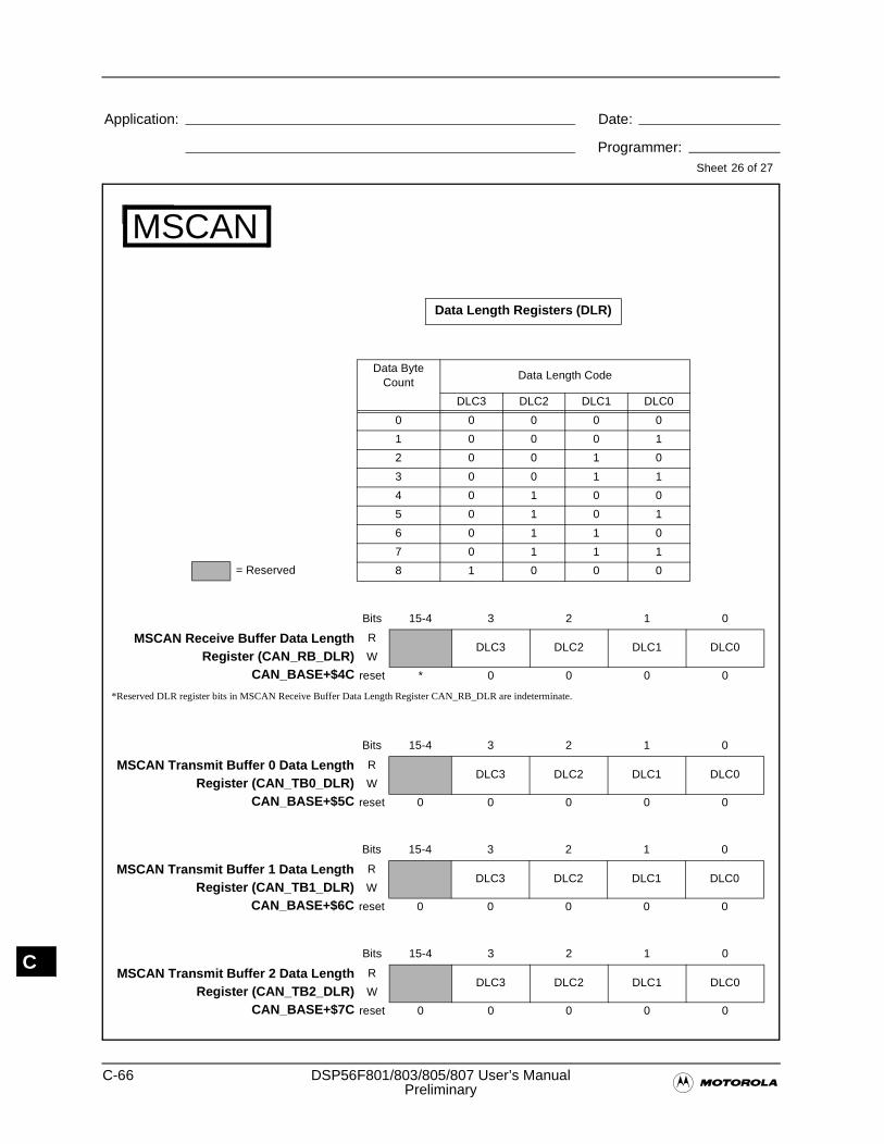
C-66 DSP56F801/803/805/807 User’s Manual�Preliminary
Application: Date:
Programmer:Sheet
C
MSCAN
26 of 27
Data Length Registers (DLR)
Data Byte Count
Data Length Code
DLC3 DLC2 DLC1 DLC0
0 0 0 0 0
1 0 0 0 1
2 0 0 1 0
3 0 0 1 1
4 0 1 0 0
5 0 1 0 1
6 0 1 1 0
7 0 1 1 1
8 1 0 0 0= Reserved
Bits 15-4 3 2 1 0
MSCAN Receive Buffer Data LengthRegister (CAN_RB_DLR)
CAN_BASE+$4C
RDLC3 DLC2 DLC1 DLC0
W
reset * 0 0 0 0
Bits 15-4 3 2 1 0
MSCAN Transmit Buffer 0 Data LengthRegister (CAN_TB0_DLR)
CAN_BASE+$5C
RDLC3 DLC2 DLC1 DLC0
W
reset 0 0 0 0 0
Bits 15-4 3 2 1 0
MSCAN Transmit Buffer 1 Data LengthRegister (CAN_TB1_DLR)
CAN_BASE+$6C
RDLC3 DLC2 DLC1 DLC0
W
reset 0 0 0 0 0
Bits 15-4 3 2 1 0
MSCAN Transmit Buffer 2 Data LengthRegister (CAN_TB2_DLR)
CAN_BASE+$7C
RDLC3 DLC2 DLC1 DLC0
W
reset 0 0 0 0 0
*Reserved DLR register bits in MSCAN Receive Buffer Data Length Register CAN_RB_DLR are indeterminate.
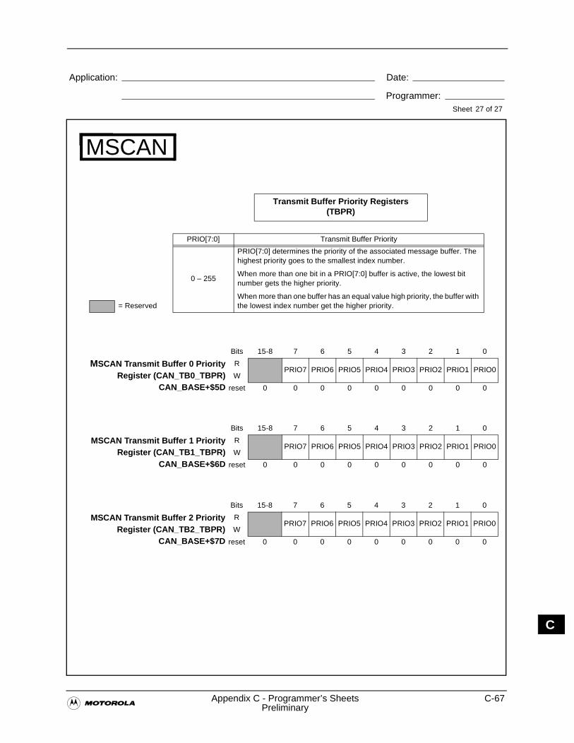
�Appendix C - Programmer’s Sheets C-67
Preliminary
Application: Date:
Programmer:Sheet
C
MSCAN
27 of 27
PRIO[7:0] Transmit Buffer Priority
0 – 255
PRIO[7:0] determines the priority of the associated message buffer. The highest priority goes to the smallest index number.
When more than one bit in a PRIO[7:0] buffer is active, the lowest bit number gets the higher priority.
When more than one buffer has an equal value high priority, the buffer with the lowest index number get the higher priority.
Bits 15-8 7 6 5 4 3 2 1 0
MSCAN Transmit Buffer 0 PriorityRegister (CAN_TB0_TBPR)
CAN_BASE+$5D
RPRIO7 PRIO6 PRIO5 PRIO4 PRIO3 PRIO2 PRIO1 PRIO0
W
reset 0 0 0 0 0 0 0 0 0
Transmit Buffer Priority Registers (TBPR)
= Reserved
Bits 15-8 7 6 5 4 3 2 1 0
MSCAN Transmit Buffer 1 PriorityRegister (CAN_TB1_TBPR)
CAN_BASE+$6D
RPRIO7 PRIO6 PRIO5 PRIO4 PRIO3 PRIO2 PRIO1 PRIO0
W
reset 0 0 0 0 0 0 0 0 0
Bits 15-8 7 6 5 4 3 2 1 0
MSCAN Transmit Buffer 2 PriorityRegister (CAN_TB2_TBPR)
CAN_BASE+$7D
RPRIO7 PRIO6 PRIO5 PRIO4 PRIO3 PRIO2 PRIO1 PRIO0
W
reset 0 0 0 0 0 0 0 0 0
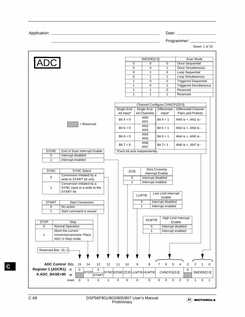
C-68 DSP56F801/803/805/807 User’s Manual�Preliminary
Application: Date:
Programmer:Sheet
C
ADC
ADC ControlRegister 1 (ADCR1)
X:ADC_BASE+$0
Bits 15 14 13 12 11 10 9 8 7 6 5 4 3 2 1 0
R 0STOP
0SYNCEOSIE ZCIE LLMTIE HLMTIE CHNCFG[3:0]
0SMODE[2:0]
W START
reset 0 1 0 1 0 0 0 0 0 0 0 0 0 1 0 1
Reserved Bits: 15, 3
1 of 10
STOP Stop 0 Normal Operation
1Abort the current conversion process. Place ADC in Stop mode.
SYNC SYNC Select
0Conversion initiated by a write to START bit only
1Conversion initiated by a SYNC input or a write to the START bit
START Start Conversion0 No action1 Start command is issued
EOSIE End of Scan Interrupt Enable0 Interrupt disabled1 Interrupt enabled
ZCIEZero Crossing
Interrupt Enable0 Interrupt disabled1 Interrupt enabled
HLMTIEHigh Limit Interrupt
Enable0 Interrupt disabled1 Interrupt enabled
LLMTIELow Limit Interrupt
Enable0 Interrupt disabled1 Interrupt enabled
SMODE[2:0] Scan Mode0 0 0 Once Sequential 0 0 1 Once Simultaneous0 1 0 Loop Sequential 0 1 1 Loop Simultaneous1 0 0 Triggered Sequential1 0 1 Triggered Simultaneous1 1 0 Reserved1 1 1 Reserved
Channel Configure CHNCFG[3:0]Single End-
ed Input*Single End-ed Channels
Differential Input*
Differential Channel Pairs and Polarity
Bit 4 = 0AN0AN1
Bit 4 = 1 AN0 is +, AN1 is -
Bit 5 = 0AN2AN3
Bit 5 = 1 AN2 is +, AN3 is -
Bit 6 = 0AN4AN5
Bit 6 = 1 AN4 is +, AN5 is -
Bit 7 = 0AN6AN7
Bit 7= 1 AN6 is +, AN7 is -
*Each bit acts independently.
= Reserved
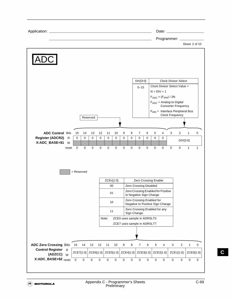
�Appendix C - Programmer’s Sheets C-69
Preliminary
Application: Date:
Programmer:Sheet
C
ADC ControlRegister (ADCR2)X:ADC_BASE+$1
Bits 15 14 13 12 11 10 9 8 7 6 5 4 3 2 1 0
R 0 0 0 0 0 0 0 0 0 0 0 0DIV[3:0]
W
reset 0 0 0 0 0 0 0 0 0 0 0 0 0 0 1 1
DIV[3:0] Clock Divisor Select
0–15 Clock Divisor Select Value =
N = DIV + 1
FADC = (FIPR) / 2N
FADC = Analog-to-Digital Converter Frequency
FIPR = Interface Peripheral Bus Clock Frequency
Reserved
ADC
2 of 10
ADC Zero CrossingControl Register
(ADZCC)X:ADC_BASE+$2
Bits 15 14 13 12 11 10 9 8 7 6 5 4 3 2 1 0
RZCE7[1:0] ZCE6[1:0] ZCE5[1:0] ZCE4[1:0] ZCE3[1:0] ZCE2[1:0] ZCE1[1:0] ZCE0[1:0]
W
reset 0 0 0 0 0 0 0 0 0 0 0 0 0 0 0 0
ZCEx[1:0] Zero Crossing Enable
00 Zero Crossing Disabled
01Zero Crossing Enabled for Positive to Negative Sign Change
10Zero Crossing Enabled for Negative to Positive Sign Change
11Zero Crossing Enabled for any Sign Change
Note: ZCE0 uses sample in ADRSLT0
ZCE7 uses sample in ADRSLT7
= Reserved
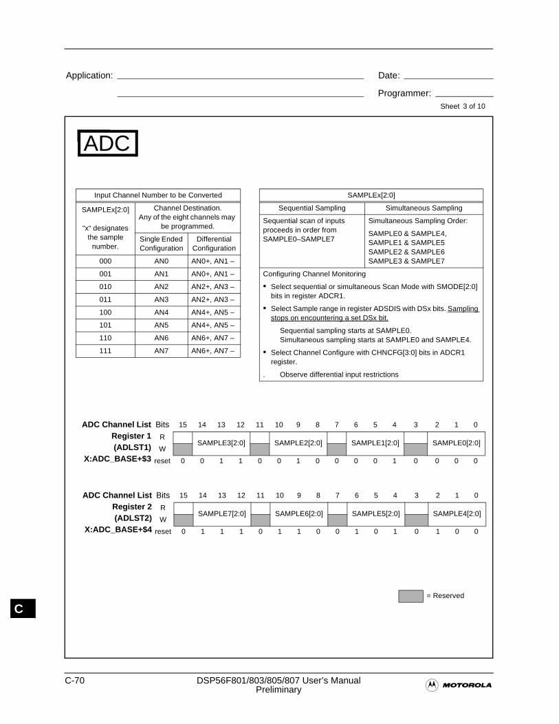
C-70 DSP56F801/803/805/807 User’s Manual�Preliminary
Application: Date:
Programmer:Sheet
C
ADC
3 of 10
ADC Channel ListRegister 2(ADLST2)
X:ADC_BASE+$4
Bits 15 14 13 12 11 10 9 8 7 6 5 4 3 2 1 0
RSAMPLE7[2:0] SAMPLE6[2:0] SAMPLE5[2:0] SAMPLE4[2:0]
W
reset 0 1 1 1 0 1 1 0 0 1 0 1 0 1 0 0
SAMPLEx[2:0]
Sequential Sampling Simultaneous Sampling
Sequential scan of inputs proceeds in order from SAMPLE0–SAMPLE7
Simultaneous Sampling Order:
SAMPLE0 & SAMPLE4,SAMPLE1 & SAMPLE5SAMPLE2 & SAMPLE6SAMPLE3 & SAMPLE7
Configuring Channel Monitoring
• Select sequential or simultaneous Scan Mode with SMODE[2:0] bits in register ADCR1.
• Select Sample range in register ADSDIS with DSx bits. Sampling stops on encountering a set DSx bit.
Sequential sampling starts at SAMPLE0.Simultaneous sampling starts at SAMPLE0 and SAMPLE4.
• Select Channel Configure with CHNCFG[3:0] bits in ADCR1 register.
. Observe differential input restrictions
ADC Channel ListRegister 1(ADLST1)
X:ADC_BASE+$3
Bits 15 14 13 12 11 10 9 8 7 6 5 4 3 2 1 0
RSAMPLE3[2:0] SAMPLE2[2:0] SAMPLE1[2:0] SAMPLE0[2:0]
W
reset 0 0 1 1 0 0 1 0 0 0 0 1 0 0 0 0
Input Channel Number to be Converted
SAMPLEx[2:0]
“x“ designates the sample
number.
Channel Destination. Any of the eight channels may
be programmed.
Single Ended Configuration
Differential Configuration
000 AN0 AN0+, AN1 –
001 AN1 AN0+, AN1 –
010 AN2 AN2+, AN3 –
011 AN3 AN2+, AN3 –
100 AN4 AN4+, AN5 –
101 AN5 AN4+, AN5 –
110 AN6 AN6+, AN7 –
111 AN7 AN6+, AN7 –
= Reserved
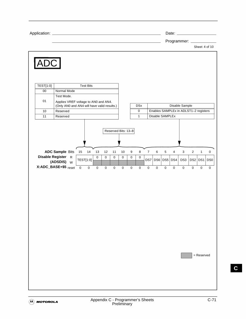
�Appendix C - Programmer’s Sheets C-71
Preliminary
Application: Date:
Programmer:Sheet
C
ADC SampleDisable Register
(ADSDIS)X:ADC_BASE+$5
Bits 15 14 13 12 11 10 9 8 7 6 5 4 3 2 1 0
RTEST[1:0]
0 0 0 0 0 0DS7 DS6 DS5 DS4 DS3 DS2 DS1 DS0
W
reset 0 0 0 0 0 0 0 0 0 0 0 0 0 0 0 0
TEST[1:0] Test Bits
00 Normal Mode
01
Test Mode.
Applies VREF voltage to AN0 and AN4. (Only AN0 and AN4 will have valid results.)
10 Reserved
11 Reserved
ADC
4 of 10
DSx Disable Sample
0 Enables SAMPLEx in ADLST1–2 registers
1 Disable SAMPLEx
Reserved Bits: 13–8
= Reserved
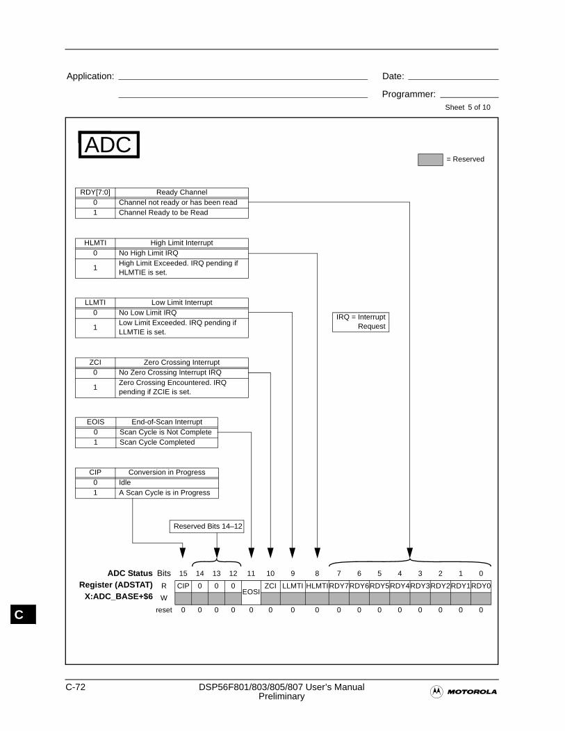
C-72 DSP56F801/803/805/807 User’s Manual�Preliminary
Application: Date:
Programmer:Sheet
C
ADC
ADC StatusRegister (ADSTAT)
X:ADC_BASE+$6
Bits 15 14 13 12 11 10 9 8 7 6 5 4 3 2 1 0
R CIP 0 0 0EOSI
ZCI LLMTI HLMTIRDY7RDY6RDY5RDY4RDY3RDY2RDY1RDY0
W
reset 0 0 0 0 0 0 0 0 0 0 0 0 0 0 0 0
Reserved Bits 14–12
5 of 10
ZCI Zero Crossing Interrupt0 No Zero Crossing Interrupt IRQ
1Zero Crossing Encountered. IRQ pending if ZCIE is set.
EOIS End-of-Scan Interrupt0 Scan Cycle is Not Complete1 Scan Cycle Completed
LLMTI Low Limit Interrupt0 No Low Limit IRQ
1Low Limit Exceeded. IRQ pending if LLMTIE is set.
RDY[7:0] Ready Channel0 Channel not ready or has been read1 Channel Ready to be Read
CIP Conversion in Progress0 Idle1 A Scan Cycle is in Progress
HLMTI High Limit Interrupt0 No High Limit IRQ
1High Limit Exceeded. IRQ pending if HLMTIE is set.
ADC
IRQ = InterruptRequest
= Reserved
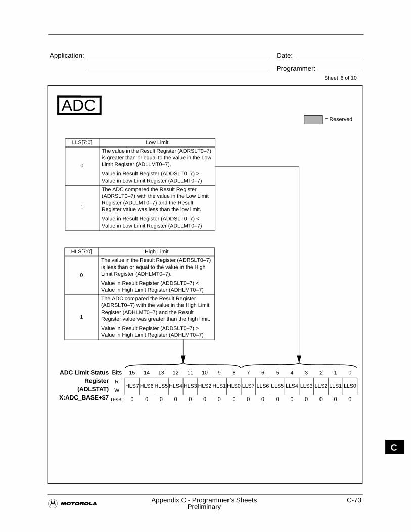
�Appendix C - Programmer’s Sheets C-73
Preliminary
Application: Date:
Programmer:Sheet
C
ADC Limit StatusRegister
(ADLSTAT)X:ADC_BASE+$7
Bits 15 14 13 12 11 10 9 8 7 6 5 4 3 2 1 0
RHLS7 HLS6 HLS5 HLS4 HLS3 HLS2 HLS1 HLS0 LLS7 LLS6 LLS5 LLS4 LLS3 LLS2 LLS1 LLS0
W
reset 0 0 0 0 0 0 0 0 0 0 0 0 0 0 0 0
HLS[7:0] High Limit
0
The value in the Result Register (ADRSLT0–7) is less than or equal to the value in the High Limit Register (ADHLMT0–7).
Value in Result Register (ADDSLT0–7) < Value in High Limit Register (ADHLMT0–7)
1
The ADC compared the Result Register (ADRSLT0–7) with the value in the High Limit Register (ADHLMT0–7) and the Result Register value was greater than the high limit.
Value in Result Register (ADDSLT0–7) > Value in High Limit Register (ADHLMT0–7)
ADC
6 of 10
LLS[7:0] Low Limit
0
The value in the Result Register (ADRSLT0–7) is greater than or equal to the value in the Low Limit Register (ADLLMT0–7).
Value in Result Register (ADDSLT0–7) > Value in Low Limit Register (ADLLMT0–7)
1
The ADC compared the Result Register (ADRSLT0–7) with the value in the Low Limit Register (ADLLMT0–7) and the Result Register value was less than the low limit.
Value in Result Register (ADDSLT0–7) < Value in Low Limit Register (ADLLMT0–7)
= Reserved
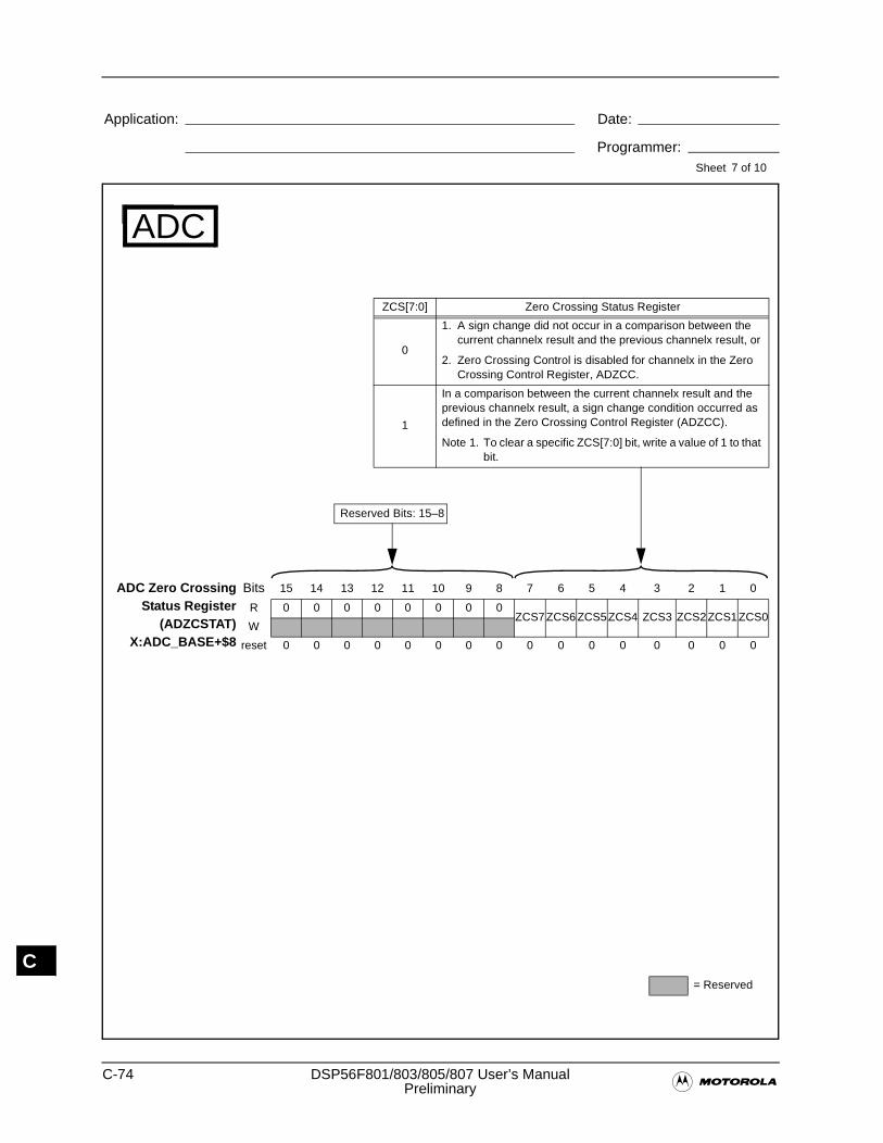
C-74 DSP56F801/803/805/807 User’s Manual�Preliminary
Application: Date:
Programmer:Sheet
C
ADC Zero CrossingStatus Register
(ADZCSTAT)X:ADC_BASE+$8
Bits 15 14 13 12 11 10 9 8 7 6 5 4 3 2 1 0
R 0 0 0 0 0 0 0 0ZCS7 ZCS6 ZCS5ZCS4 ZCS3 ZCS2ZCS1ZCS0
W
reset 0 0 0 0 0 0 0 0 0 0 0 0 0 0 0 0
ADC
7 of 10
ZCS[7:0] Zero Crossing Status Register
0
1. A sign change did not occur in a comparison between the current channelx result and the previous channelx result, or
2. Zero Crossing Control is disabled for channelx in the Zero Crossing Control Register, ADZCC.
1
In a comparison between the current channelx result and the previous channelx result, a sign change condition occurred as defined in the Zero Crossing Control Register (ADZCC).
Note 1. To clear a specific ZCS[7:0] bit, write a value of 1 to that bit.
Reserved Bits: 15–8
= Reserved
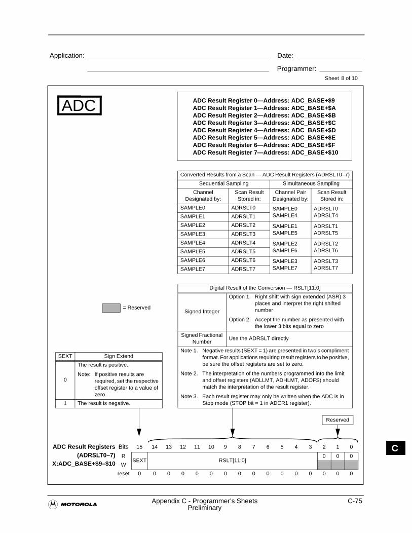
�Appendix C - Programmer’s Sheets C-75
Preliminary
Application: Date:
Programmer:Sheet
C
ADC
8 of 10
ADC Result Register 0—Address: ADC_BASE+$9ADC Result Register 1—Address: ADC_BASE+$AADC Result Register 2—Address: ADC_BASE+$BADC Result Register 3—Address: ADC_BASE+$CADC Result Register 4—Address: ADC_BASE+$DADC Result Register 5—Address: ADC_BASE+$EADC Result Register 6—Address: ADC_BASE+$FADC Result Register 7—Address: ADC_BASE+$10
ADC Result Registers(ADRSLT0–7)
X:ADC_BASE+$9–$10
Bits 15 14 13 12 11 10 9 8 7 6 5 4 3 2 1 0
RSEXT RSLT[11:0]
0 0 0
W
reset 0 0 0 0 0 0 0 0 0 0 0 0 0 0 0 0
Digital Result of the Conversion — RSLT[11:0]
Signed Integer
Option 1. Right shift with sign extended (ASR) 3 places and interpret the right shifted number
Option 2. Accept the number as presented with the lower 3 bits equal to zero
Signed Fractional Number
Use the ADRSLT directly
Note 1. Negative results (SEXT = 1) are presented in two’s compliment format. For applications requiring result registers to be positive, be sure the offset registers are set to zero.
Note 2. The interpretation of the numbers programmed into the limit and offset registers (ADLLMT, ADHLMT, ADOFS) should match the interpretation of the result register.
Note 3. Each result register may only be written when the ADC is in Stop mode (STOP bit = 1 in ADCR1 register).
Converted Results from a Scan — ADC Result Registers (ADRSLT0–7)
Sequential Sampling Simultaneous Sampling
Channel Designated by:
Scan Result Stored in:
Channel Pair Designated by:
Scan Result Stored in:
SAMPLE0 ADRSLT0 SAMPLE0SAMPLE4
ADRSLT0ADRSLT4SAMPLE1 ADRSLT1
SAMPLE2 ADRSLT2 SAMPLE1SAMPLE5
ADRSLT1ADRSLT5SAMPLE3 ADRSLT3
SAMPLE4 ADRSLT4 SAMPLE2SAMPLE6
ADRSLT2ADRSLT6SAMPLE5 ADRSLT5
SAMPLE6 ADRSLT6 SAMPLE3SAMPLE7
ADRSLT3ADRSLT7SAMPLE7 ADRSLT7
SEXT Sign Extend
0
The result is positive.
Note: If positive results are required, set the respective offset register to a value of zero.
1 The result is negative.
Reserved
= Reserved
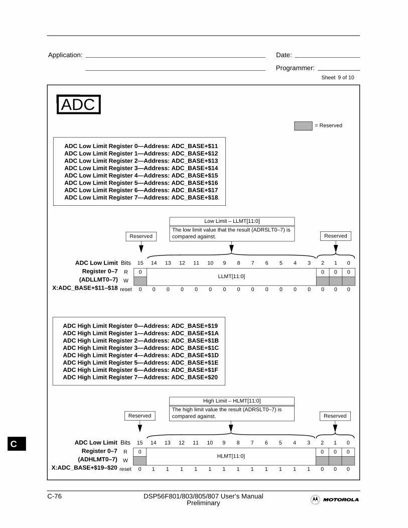
C-76 DSP56F801/803/805/807 User’s Manual�Preliminary
Application: Date:
Programmer:Sheet
C
ADC
9 of 10
ADC Low Limit Register 0—Address: ADC_BASE+$11ADC Low Limit Register 1—Address: ADC_BASE+$12ADC Low Limit Register 2—Address: ADC_BASE+$13ADC Low Limit Register 3—Address: ADC_BASE+$14ADC Low Limit Register 4—Address: ADC_BASE+$15ADC Low Limit Register 5—Address: ADC_BASE+$16ADC Low Limit Register 6—Address: ADC_BASE+$17ADC Low Limit Register 7—Address: ADC_BASE+$18 .
Low Limit – LLMT[11:0]
The low limit value that the result (ADRSLT0–7) is compared against.
ADC Low LimitRegister 0–7
(ADLLMT0–7)X:ADC_BASE+$11–$18
Bits 15 14 13 12 11 10 9 8 7 6 5 4 3 2 1 0
R 0LLMT[11:0]
0 0 0
W
reset 0 0 0 0 0 0 0 0 0 0 0 0 0 0 0 0
ADC High Limit Register 0—Address: ADC_BASE+$19ADC High Limit Register 1—Address: ADC_BASE+$1AADC High Limit Register 2—Address: ADC_BASE+$1BADC High Limit Register 3—Address: ADC_BASE+$1CADC High Limit Register 4—Address: ADC_BASE+$1DADC High Limit Register 5—Address: ADC_BASE+$1EADC High Limit Register 6—Address: ADC_BASE+$1FADC High Limit Register 7—Address: ADC_BASE+$20
High Limit – HLMT[11:0]
The high limit value the result (ADRSLT0–7) is compared against.
ADC Low LimitRegister 0–7
(ADHLMT0–7)X:ADC_BASE+$19–$20
Bits 15 14 13 12 11 10 9 8 7 6 5 4 3 2 1 0
R 0HLMT[11:0]
0 0 0
W
reset 0 1 1 1 1 1 1 1 1 1 1 1 1 0 0 0
Reserved
Reserved
Reserved
Reserved
= Reserved
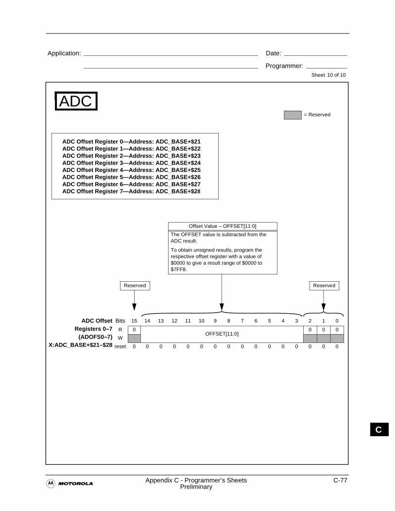
�Appendix C - Programmer’s Sheets C-77
Preliminary
Application: Date:
Programmer:Sheet
C
ADC
10 of 10
ADC Offset Register 0—Address: ADC_BASE+$21ADC Offset Register 1—Address: ADC_BASE+$22ADC Offset Register 2—Address: ADC_BASE+$23ADC Offset Register 3—Address: ADC_BASE+$24ADC Offset Register 4—Address: ADC_BASE+$25ADC Offset Register 5—Address: ADC_BASE+$26ADC Offset Register 6—Address: ADC_BASE+$27ADC Offset Register 7—Address: ADC_BASE+$2 8
ADC OffsetRegisters 0–7
(ADOFS0–7)X:ADC_BASE+$21–$28
Bits 15 14 13 12 11 10 9 8 7 6 5 4 3 2 1 0
R 0OFFSET[11:0]
0 0 0
W
reset 0 0 0 0 0 0 0 0 0 0 0 0 0 0 0 0
ReservedReserved
Offset Value – OFFSET[11:0]
The OFFSET value is subtracted from the ADC result.
To obtain unsigned results, program the respective offset register with a value of $0000 to give a result range of $0000 to $7FF8.
= Reserved
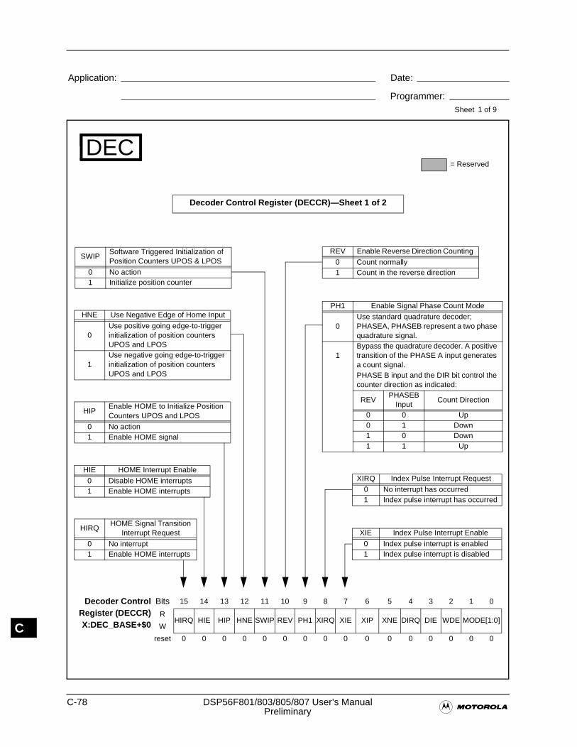
C-78 DSP56F801/803/805/807 User’s Manual�Preliminary
Application: Date:
Programmer:Sheet
C
HIE HOME Interrupt Enable
0 Disable HOME interrupts1 Enable HOME interrupts
HNE Use Negative Edge of Home Input
0Use positive going edge-to-trigger initialization of position counters UPOS and LPOS
1Use negative going edge-to-trigger initialization of position counters UPOS and LPOS
HIPEnable HOME to Initialize Position Counters UPOS and LPOS
0 No action1 Enable HOME signal
SWIPSoftware Triggered Initialization of Position Counters UPOS & LPOS
0 No action1 Initialize position counter
XIRQ Index Pulse Interrupt Request
0 No interrupt has occurred1 Index pulse interrupt has occurred
REV Enable Reverse Direction Counting
0 Count normally1 Count in the reverse direction
PH1 Enable Signal Phase Count Mode
0Use standard quadrature decoder; PHASEA, PHASEB represent a two phase quadrature signal.
1Bypass the quadrature decoder. A positive transition of the PHASE A input generates a count signal. PHASE B input and the DIR bit control the counter direction as indicated:
REVPHASEB
InputCount Direction
0 0 Up0 1 Down1 0 Down1 1 Up
HIRQHOME Signal Transition
Interrupt Request
0 No interrupt1 Enable HOME interrupts
Decoder ControlRegister (DECCR)X:DEC_BASE+$0
Bits 15 14 13 12 11 10 9 8 7 6 5 4 3 2 1 0
RHIRQ HIE HIP HNE SWIP REV PH1 XIRQ XIE XIP XNE DIRQ DIE WDE MODE[1:0]
W
reset 0 0 0 0 0 0 0 0 0 0 0 0 0 0 0 0
XIE Index Pulse Interrupt Enable
0 Index pulse interrupt is enabled1 Index pulse interrupt is disabled
DEC
1 of 9
Decoder Control Register (DECCR)—Sheet 1 of 2
= Reserved
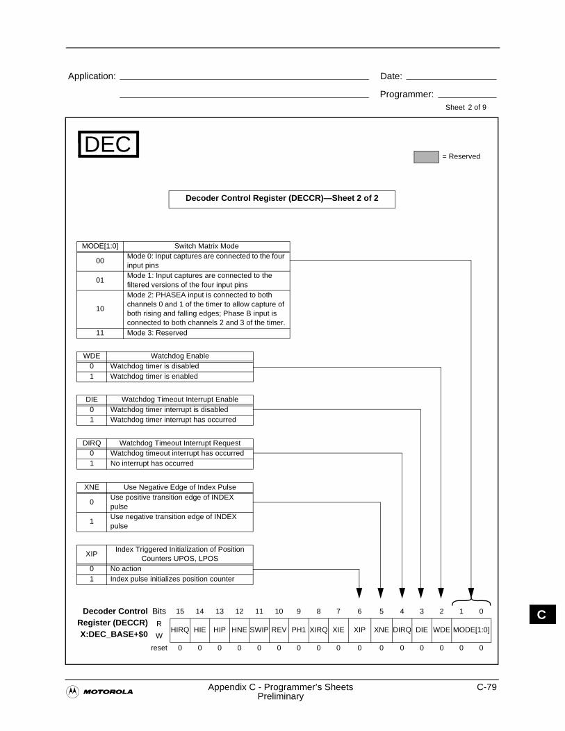
�Appendix C - Programmer’s Sheets C-79
Preliminary
Application: Date:
Programmer:Sheet
CDecoder ControlRegister (DECCR)X:DEC_BASE+$0
Bits 15 14 13 12 11 10 9 8 7 6 5 4 3 2 1 0
RHIRQ HIE HIP HNE SWIP REV PH1 XIRQ XIE XIP XNE DIRQ DIE WDE MODE[1:0]
W
reset 0 0 0 0 0 0 0 0 0 0 0 0 0 0 0 0
DIRQ Watchdog Timeout Interrupt Request0 Watchdog timeout interrupt has occurred1 No interrupt has occurred
DIE Watchdog Timeout Interrupt Enable0 Watchdog timer interrupt is disabled1 Watchdog timer interrupt has occurred
WDE Watchdog Enable0 Watchdog timer is disabled1 Watchdog timer is enabled
XNE Use Negative Edge of Index Pulse
0Use positive transition edge of INDEX pulse
1Use negative transition edge of INDEX pulse
MODE[1:0] Switch Matrix Mode
00Mode 0: Input captures are connected to the four input pins
01Mode 1: Input captures are connected to the filtered versions of the four input pins
10
Mode 2: PHASEA input is connected to both channels 0 and 1 of the timer to allow capture of both rising and falling edges; Phase B input is connected to both channels 2 and 3 of the timer.
11 Mode 3: Reserved
DEC
2 of 9
XIPIndex Triggered Initialization of Position
Counters UPOS, LPOS0 No action1 Index pulse initializes position counter
Decoder Control Register (DECCR)—Sheet 2 of 2
= Reserved
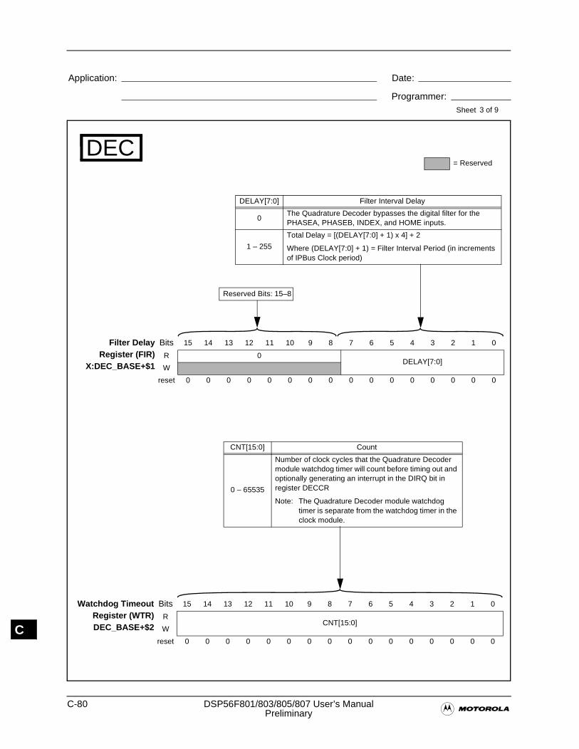
C-80 DSP56F801/803/805/807 User’s Manual�Preliminary
Application: Date:
Programmer:Sheet
C
Filter DelayRegister (FIR)
X:DEC_BASE+$1
Bits 15 14 13 12 11 10 9 8 7 6 5 4 3 2 1 0
R 0DELAY[7:0]
W
reset 0 0 0 0 0 0 0 0 0 0 0 0 0 0 0 0
DELAY[7:0] Filter Interval Delay
0The Quadrature Decoder bypasses the digital filter for the PHASEA, PHASEB, INDEX, and HOME inputs.
1 – 255
Total Delay = [(DELAY[7:0] + 1) x 4] + 2
Where (DELAY[7:0] + 1) = Filter Interval Period (in increments of IPBus Clock period)
Reserved Bits: 15–8
Watchdog TimeoutRegister (WTR)DEC_BASE+$2
Bits 15 14 13 12 11 10 9 8 7 6 5 4 3 2 1 0
RCNT[15:0]
W
reset 0 0 0 0 0 0 0 0 0 0 0 0 0 0 0 0
CNT[15:0] Count
0 – 65535
Number of clock cycles that the Quadrature Decoder module watchdog timer will count before timing out and optionally generating an interrupt in the DIRQ bit in register DECCR
Note: The Quadrature Decoder module watchdog timer is separate from the watchdog timer in the clock module.
DEC
3 of 9
= Reserved
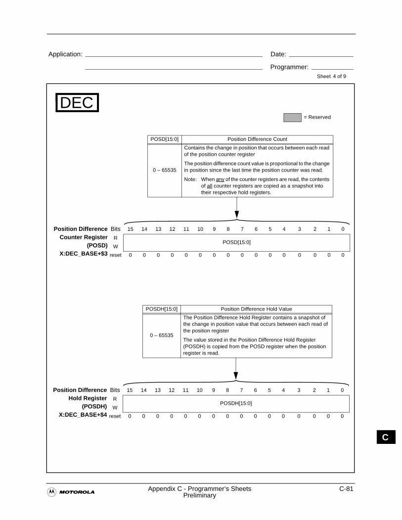
�Appendix C - Programmer’s Sheets C-81
Preliminary
Application: Date:
Programmer:Sheet
C
Position DifferenceCounter Register
(POSD)X:DEC_BASE+$3
Bits 15 14 13 12 11 10 9 8 7 6 5 4 3 2 1 0
RPOSD[15:0]
W
reset 0 0 0 0 0 0 0 0 0 0 0 0 0 0 0 0
POSD[15:0] Position Difference Count
0 – 65535
Contains the change in position that occurs between each read of the position counter register
The position difference count value is proportional to the change in position since the last time the position counter was read.
Note: When any of the counter registers are read, the contents of all counter registers are copied as a snapshot into their respective hold registers.
Position DifferenceHold Register
(POSDH)X:DEC_BASE+$4
Bits 15 14 13 12 11 10 9 8 7 6 5 4 3 2 1 0
RPOSDH[15:0]
W
reset 0 0 0 0 0 0 0 0 0 0 0 0 0 0 0 0
POSDH[15:0] Position Difference Hold Value
0 – 65535
The Position Difference Hold Register contains a snapshot of the change in position value that occurs between each read of the position register
The value stored in the Position Difference Hold Register (POSDH) is copied from the POSD register when the position register is read.
DEC
4 of 9
= Reserved
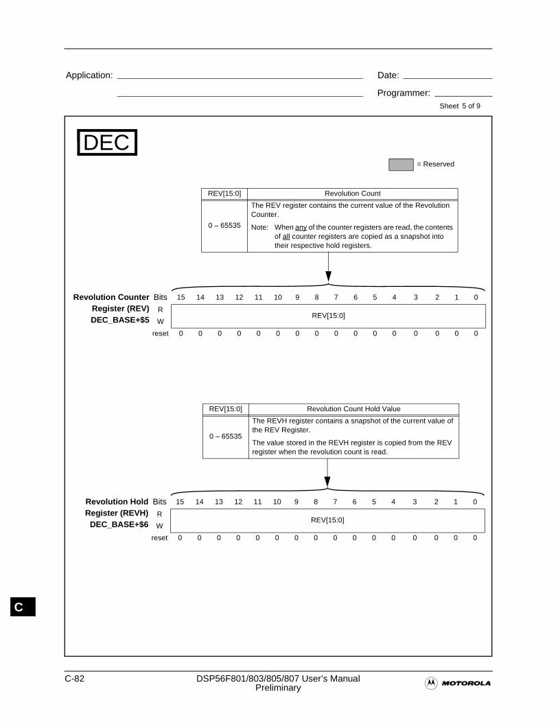
C-82 DSP56F801/803/805/807 User’s Manual�Preliminary
Application: Date:
Programmer:Sheet
C
Revolution CounterRegister (REV)DEC_BASE+$5
Bits 15 14 13 12 11 10 9 8 7 6 5 4 3 2 1 0
RREV[15:0]
W
reset 0 0 0 0 0 0 0 0 0 0 0 0 0 0 0 0
REV[15:0] Revolution Count
0 – 65535
The REV register contains the current value of the Revolution Counter.
Note: When any of the counter registers are read, the contents of all counter registers are copied as a snapshot into their respective hold registers.
Revolution HoldRegister (REVH)
DEC_BASE+$6
Bits 15 14 13 12 11 10 9 8 7 6 5 4 3 2 1 0
RREV[15:0]
W
reset 0 0 0 0 0 0 0 0 0 0 0 0 0 0 0 0
REV[15:0] Revolution Count Hold Value
0 – 65535
The REVH register contains a snapshot of the current value of the REV Register.
The value stored in the REVH register is copied from the REV register when the revolution count is read.
DEC
5 of 9
= Reserved
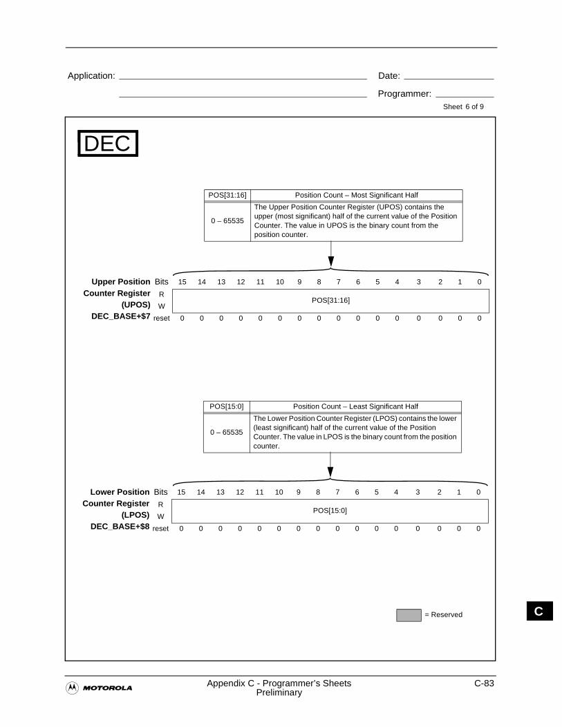
�Appendix C - Programmer’s Sheets C-83
Preliminary
Application: Date:
Programmer:Sheet
C
Upper PositionCounter Register
(UPOS)DEC_BASE+$7
Bits 15 14 13 12 11 10 9 8 7 6 5 4 3 2 1 0
RPOS[31:16]
W
reset 0 0 0 0 0 0 0 0 0 0 0 0 0 0 0 0
POS[31:16] Position Count – Most Significant Half
0 – 65535
The Upper Position Counter Register (UPOS) contains the upper (most significant) half of the current value of the Position Counter. The value in UPOS is the binary count from the position counter.
Lower PositionCounter Register
(LPOS)DEC_BASE+$8
Bits 15 14 13 12 11 10 9 8 7 6 5 4 3 2 1 0
RPOS[15:0]
W
reset 0 0 0 0 0 0 0 0 0 0 0 0 0 0 0 0
POS[15:0] Position Count – Least Significant Half
0 – 65535
The Lower Position Counter Register (LPOS) contains the lower (least significant) half of the current value of the Position Counter. The value in LPOS is the binary count from the position counter.
DEC
6 of 9
= Reserved

C-84 DSP56F801/803/805/807 User’s Manual�Preliminary
Application: Date:
Programmer:Sheet
C
Upper PositionHold Register
(UPOSH)DEC_BASE+$9
Bits 15 14 13 12 11 10 9 8 7 6 5 4 3 2 1 0
RPOS[31:16]
W
reset 0 0 0 0 0 0 0 0 0 0 0 0 0 0 0 0
Lower PositionHold Register
(LPOSH)DEC_BASE+$A
Bits 15 14 13 12 11 10 9 8 7 6 5 4 3 2 1 0
RPOS[15:0]
W
reset 0 0 0 0 0 0 0 0 0 0 0 0 0 0 0 0
POS[15:0] Position Counter
0 – 65535The Position Counter is a “snapshot” of the lower (least significant) half of the current value of the Position Counter.
POS[15:0] Position Counter
0 – 65535The Position Counter is a “snapshot” of the upper (most significant) half of the current value of the Position Counter.
DEC
7 of 9
= Reserved
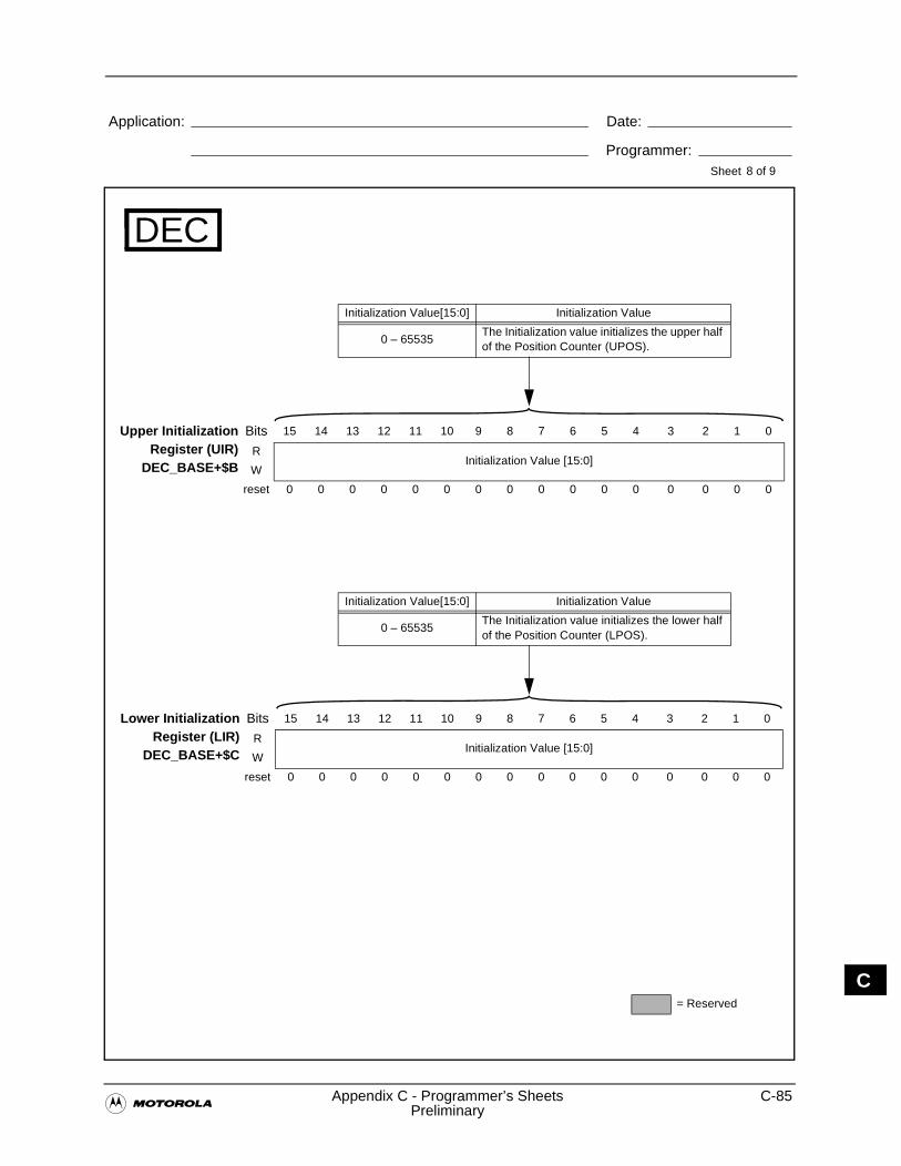
�Appendix C - Programmer’s Sheets C-85
Preliminary
Application: Date:
Programmer:Sheet
C
Upper InitializationRegister (UIR)
DEC_BASE+$B
Bits 15 14 13 12 11 10 9 8 7 6 5 4 3 2 1 0
RInitialization Value [15:0]
W
reset 0 0 0 0 0 0 0 0 0 0 0 0 0 0 0 0
Lower InitializationRegister (LIR)
DEC_BASE+$C
Bits 15 14 13 12 11 10 9 8 7 6 5 4 3 2 1 0
RInitialization Value [15:0]
W
reset 0 0 0 0 0 0 0 0 0 0 0 0 0 0 0 0
Initialization Value[15:0] Initialization Value
0 – 65535The Initialization value initializes the lower half of the Position Counter (LPOS).
Initialization Value[15:0] Initialization Value
0 – 65535The Initialization value initializes the upper half of the Position Counter (UPOS).
DEC
8 of 9
= Reserved
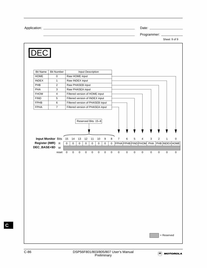
C-86 DSP56F801/803/805/807 User’s Manual�Preliminary
Application: Date:
Programmer:Sheet
C
Input MonitorRegister (IMR)
DEC_BASE+$D
Bits 15 14 13 12 11 10 9 8 7 6 5 4 3 2 1 0
R 0 0 0 0 0 0 0 0 FPHA FPHB FIND FHOM PHA PHB INDEX HOME
W
reset 0 0 0 0 0 0 0 0 0 0 0 0 0 0 0 0
Reserved Bits: 15–8
Bit Name Bit Number Input Description
HOME 0 Raw HOME input
INDEX 1 Raw INDEX input
PHB 2 Raw PHASEB input
PHA 3 Raw PHASEA input
FHOM 4 Filtered version of HOME input
FIND 5 Filtered version of INDEX input
FPHB 6 Filtered version of PHASEB input
FPHA 7 Filtered version of PHASEA input
DEC
9 of 9
= Reserved
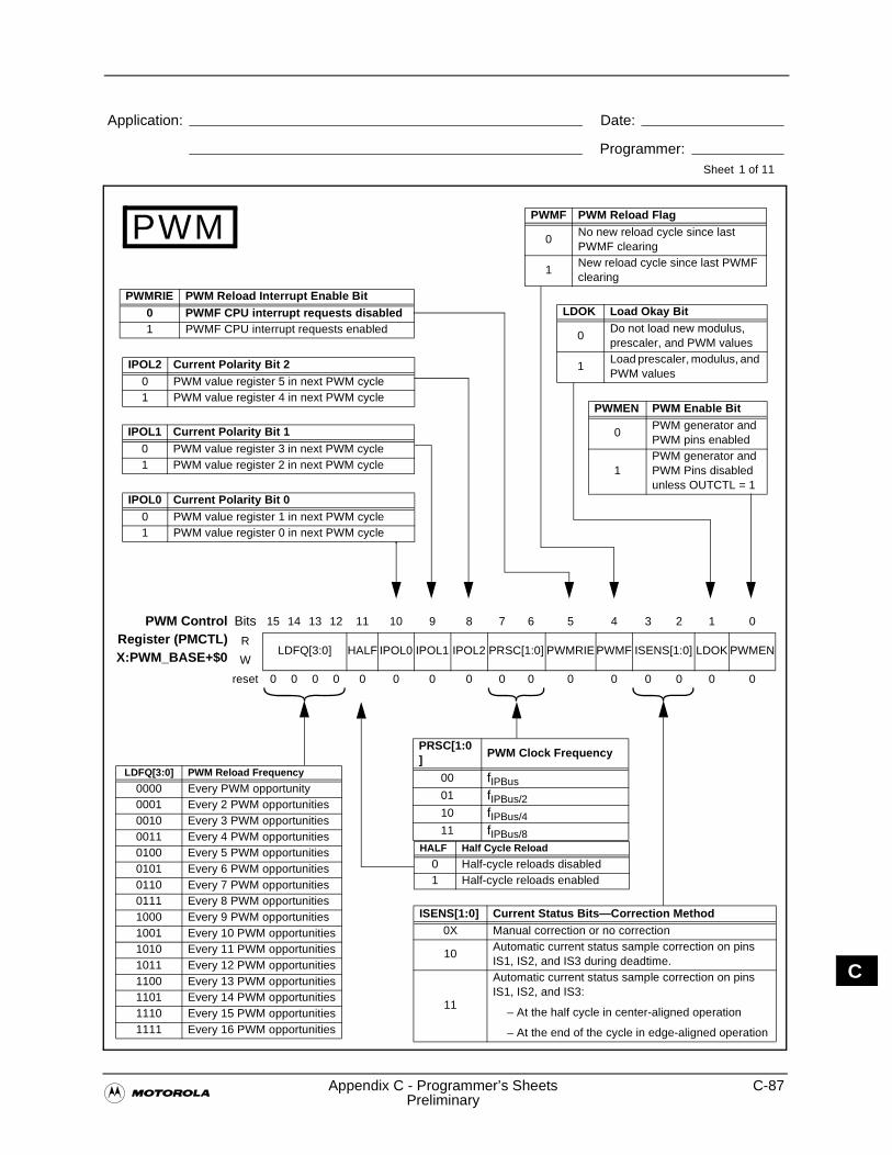
�Appendix C - Programmer’s Sheets C-87
Preliminary
Application: Date:
Programmer:Sheet
C
IPOL2 Current Polarity Bit 20 PWM value register 5 in next PWM cycle1 PWM value register 4 in next PWM cycle
PWM ControlRegister (PMCTL)X:PWM_BASE+$0
Bits 15 14 13 12 11 10 9 8 7 6 5 4 3 2 1 0
RLDFQ[3:0] HALF IPOL0 IPOL1 IPOL2 PRSC[1:0] PWMRIE PWMF ISENS[1:0] LDOK PWMEN
W
reset 0 0 0 0 0 0 0 0 0 0 0 0 0 0 0 0
PWM
1 of 11
IPOL1 Current Polarity Bit 10 PWM value register 3 in next PWM cycle1 PWM value register 2 in next PWM cycle
IPOL0 Current Polarity Bit 00 PWM value register 1 in next PWM cycle1 PWM value register 0 in next PWM cycle
HALF Half Cycle Reload
0 Half-cycle reloads disabled1 Half-cycle reloads enabled
PWMEN PWM Enable Bit
0PWM generator and PWM pins enabled
1PWM generator and PWM Pins disabled unless OUTCTL = 1
ISENS[1:0] Current Status Bits—Correction Method0X Manual correction or no correction
10Automatic current status sample correction on pins IS1, IS2, and IS3 during deadtime.
11
Automatic current status sample correction on pins IS1, IS2, and IS3:
– At the half cycle in center-aligned operation
– At the end of the cycle in edge-aligned operation
LDOK Load Okay Bit
0Do not load new modulus, prescaler, and PWM values
1Load prescaler, modulus, and PWM values
LDFQ[3:0] PWM Reload Frequency
0000 Every PWM opportunity0001 Every 2 PWM opportunities0010 Every 3 PWM opportunities0011 Every 4 PWM opportunities0100 Every 5 PWM opportunities0101 Every 6 PWM opportunities0110 Every 7 PWM opportunities0111 Every 8 PWM opportunities1000 Every 9 PWM opportunities1001 Every 10 PWM opportunities1010 Every 11 PWM opportunities1011 Every 12 PWM opportunities1100 Every 13 PWM opportunities1101 Every 14 PWM opportunities1110 Every 15 PWM opportunities1111 Every 16 PWM opportunities
PRSC[1:0]
PWM Clock Frequency
00 fIPBus01 fIPBus/210 fIPBus/411 fIPBus/8
PWMRIE PWM Reload Interrupt Enable Bit 0 PWMF CPU interrupt requests disabled1 PWMF CPU interrupt requests enabled
PWMF PWM Reload Flag
0No new reload cycle since last PWMF clearing
1New reload cycle since last PWMF clearing
Appendix C

C-88 DSP56F801/803/805/807 User’s Manual�Preliminary
Application: Date:
Programmer:Sheet
C
PWM
2 of 11
PWM Fault ControlRegister (PMFCTL)
PWM_BASE+$1
Bits 15 14 13 12 11 10 9 8 7 6 5 4 3 2 1 0
R 0 0 0 0 0 0 0 0FIE3 FMODE3 FIE2 FMODE2 FIE1 FMODE1 FIE0 FMODE0
W
reset 0 0 0 0 0 0 0 0
FIEx FAULTx Pin Interrupt Enable Bit—Bits 7, 5, 3, 1
0 FAULTx CPU interrupt requests disabled
1 FAULTx CPU interrupt requests enabled
Reserved Bits: 15–8
FMODEx FAULTx Pin Clearing Mode Bit—Bits 6, 4, 2, 0
0 Manual fault clearing of FAULTx pin faults
1 Automatic fault clearing of FAULTx pin faults
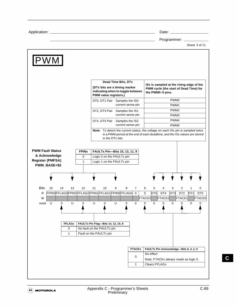
�Appendix C - Programmer’s Sheets C-89
Preliminary
Application: Date:
Programmer:Sheet
C
PWM
3 of 11
Bits 15 14 13 12 11 10 9 8 7 6 5 4 3 2 1 0
R FPIN3 FFLAG3 FPIN2 FFLAG2 FPIN1 FFLAG1 FPIN0 FFLAG0 0 0 DT5 DT4 DT3 DT2 DT1 DT0
W FTACK3 FTACK2 FTACK1 FTACK0
reset U 0 U 0 U 0 U 0 0 0 0 0 0 0 0 0
FPINx FAULTx Pin—Bits 15, 13, 11, 9
0 Logic 0 on the FAULTx pin
1 Logic 1 on the FAULTx pin
Dead Time Bits, DTx
(DTx bits are a timing marker indicating when to toggle between PWM value registers.)
ISx is sampled at the rising edge of the PWM cycle (the start of Dead Time) for the PWM0–5 pins.
DT0, DT1 Pair Samples the IS0 current sense pin
PWM0
PWM1
DT2, DT3 Pair Samples the IS1 current sense pin
PWM2
PWM3
DT4, DT5 Pair Samples the IS2 current sense pin
PWM4
PWM5
Note: To detect the current status, the voltage on each ISx pin is sampled twice in a PWM period at the end of each deadtime, and the ISx values are stored in the DTx bits.
FFLAGx FAULTx Pin Flag—Bits 14, 12, 10, 8
0 No fault on the FAULTx pin
1 Fault on the FAULTx pin
FTACKx FAULTx Pin Acknowledge—Bits 6, 4, 2, 0
0No effect
Note: FTACKx always reads as logic 0.
1 Clears FFLAGx
PWM Fault Status& Acknowledge
Register (PMFSA)PWM_BASE+$2
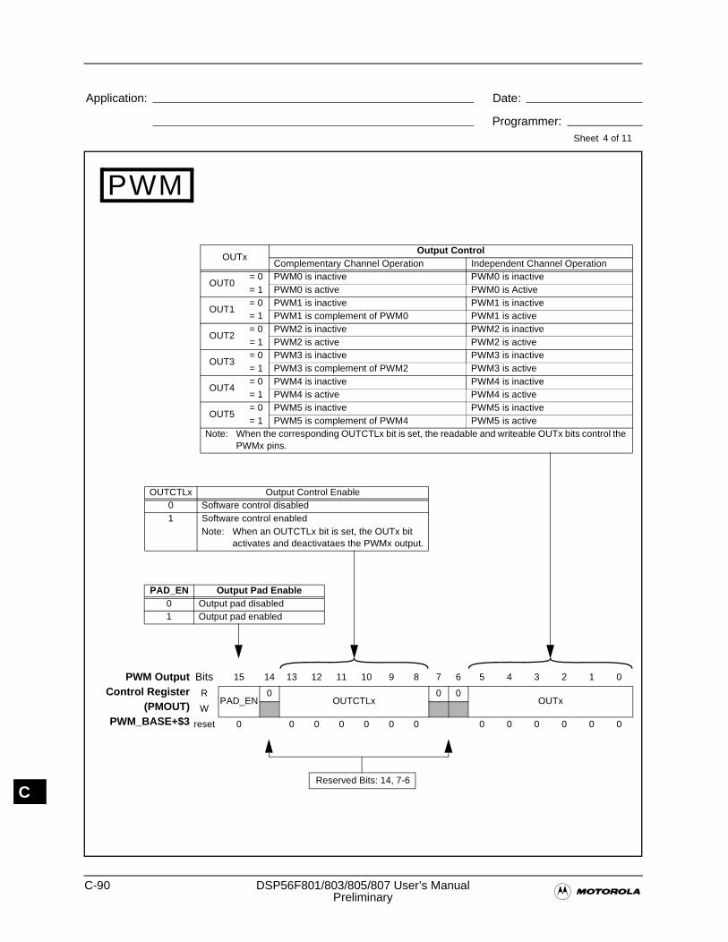
C-90 DSP56F801/803/805/807 User’s Manual�Preliminary
Application: Date:
Programmer:Sheet
C
OUTCTLx Output Control Enable0 Software control disabled1 Software control enabled
Note: When an OUTCTLx bit is set, the OUTx bit activates and deactivataes the PWMx output.
PWM OutputControl Register
(PMOUT)PWM_BASE+$3
Bits 15 14 13 12 11 10 9 8 7 6 5 4 3 2 1 0
RPAD_EN
0OUTCTLx
0 0OUTx
W
reset 0 0 0 0 0 0 0 0 0 0 0 0 0
PWM
4 of 11
PAD_EN Output Pad Enable0 Output pad disabled1 Output pad enabled
OUTx Output Control
Complementary Channel Operation Independent Channel Operation
OUT0= 0 PWM0 is inactive PWM0 is inactive= 1 PWM0 is active PWM0 is Active
OUT1= 0 PWM1 is inactive PWM1 is inactive= 1 PWM1 is complement of PWM0 PWM1 is active
OUT2= 0 PWM2 is inactive PWM2 is inactive= 1 PWM2 is active PWM2 is active
OUT3= 0 PWM3 is inactive PWM3 is inactive= 1 PWM3 is complement of PWM2 PWM3 is active
OUT4= 0 PWM4 is inactive PWM4 is inactive= 1 PWM4 is active PWM4 is active
OUT5= 0 PWM5 is inactive PWM5 is inactive= 1 PWM5 is complement of PWM4 PWM5 is active
Note: When the corresponding OUTCTLx bit is set, the readable and writeable OUTx bits control the PWMx pins.
Reserved Bits: 14, 7-6
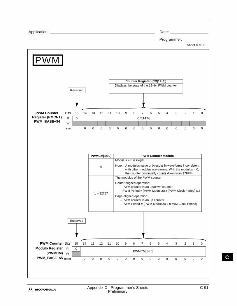
�Appendix C - Programmer’s Sheets C-91
Preliminary
Application: Date:
Programmer:Sheet
C
Counter Register (CR[14:0])Displays the state of the 15–bit PWM counter
PWM CounterRegister (PMCNT) PWM_BASE+$4
Bits 15 14 13 12 11 10 9 8 7 6 5 4 3 2 1 0
R 0 CR[14:0]
W
reset 0 0 0 0 0 0 0 0 0 0 0 0 0 0 0
PWM
5 of 11
Reserved
PWMCM[14:0] PWM Counter Modulo
0
Modulus = 0 is illegal
Note: A modulus value of 0 results in waveforms inconsistent with other modulus waveforms. With the modulus = 0, the counter continually counts down from $7FFF.
1 – 32767
The modulus of the PWM counter
Center-aligned operation:– PWM counter is an up/down counter– PWM Period = (PWM Modulus) x (PWM Clock Period) x 2
Edge-aligned operation:– PWM counter is an up counter– PWM Period = (PWM Modulus) x (PWM Clock Period)
PWM CounterModulo Register
(PWMCM)PWM_BASE+$5
Bits 15 14 13 12 11 10 9 8 7 6 5 4 3 2 1 0
R 0PWMCM[14:0]
W
reset 0 0 0 0 0 0 0 0 0 0 0 0 0 0 0
Reserved
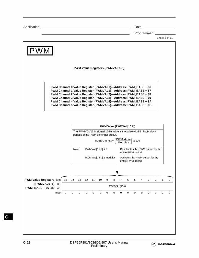
C-92 DSP56F801/803/805/807 User’s Manual�Preliminary
Application: Date:
Programmer:Sheet
C
PWM Value Registers(PWMVAL0–5)
PWM_BASE + $6–$B
Bits 15 14 13 12 11 10 9 8 7 6 5 4 3 2 1 0
RPWMVAL[15:0]
W
reset 0 0 0 0 0 0 0 0 0 0 0 0 0 0 0 0
PWM
6 of 11
PWM Channel 0 Value Register (PWMVAL0)—Address: PWM_BASE + $6 PWM Channel 1 Value Register (PWMVAL1)—Address: PWM_BASE + $7PWM Channel 2 Value Register (PWMVAL2)—Address: PWM_BASE + $8PWM Channel 3 Value Register (PWMVAL3)—Address: PWM_BASE + $9PWM Channel 4 Value Register (PWMVAL4)—Address: PWM_BASE + $APWM Channel 5 Value Register (PWMVAL5)—Address: PWM_BASE + $B
PWM Value Registers (PWMVAL0–5)
PWM Value (PWMVAL[15:0])
The PWMVAL[15:0] signed 16-bit value is the pulse width in PWM clock periods of the PWM generator output.
Note: PWMVAL[15:0] ≤ 0: Deactivates the PWM output for the entire PWM period
PWMVAL[15:0] ≥ Modulus: Activates the PWM output for the entire PWM period
DutyCycle( ) PWM ValueModulus
--------------------------------- x 100=
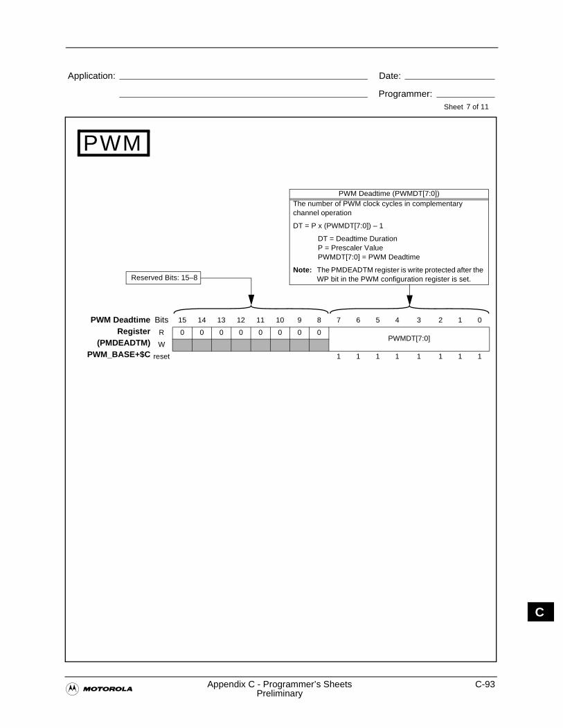
�Appendix C - Programmer’s Sheets C-93
Preliminary
Application: Date:
Programmer:Sheet
C
PWM DeadtimeRegister
(PMDEADTM)PWM_BASE+$C
Bits 15 14 13 12 11 10 9 8 7 6 5 4 3 2 1 0
R 0 0 0 0 0 0 0 0PWMDT[7:0]
W
reset 1 1 1 1 1 1 1 1
PWM
7 of 11
PWM Deadtime (PWMDT[7:0])The number of PWM clock cycles in complementary channel operation
DT = P x (PWMDT[7:0]) – 1
DT = Deadtime DurationP = Prescaler ValuePWMDT[7:0] = PWM Deadtime
Note: The PMDEADTM register is write protected after the WP bit in the PWM configuration register is set. Reserved Bits: 15–8
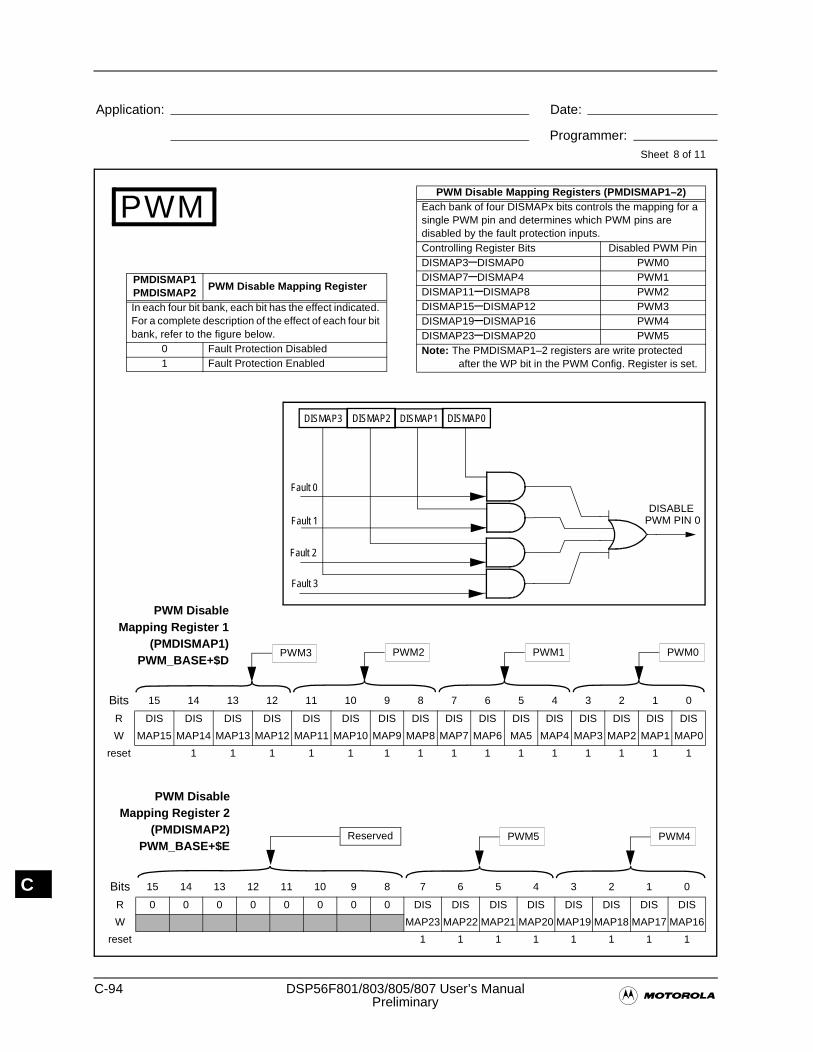
C-94 DSP56F801/803/805/807 User’s Manual�Preliminary
Application: Date:
Programmer:Sheet
C
PWM
8 of 11
PWM DisableMapping Register 1
(PMDISMAP1)PWM_BASE+$D
Bits 15 14 13 12 11 10 9 8 7 6 5 4 3 2 1 0
R DIS
MAP15
DIS
MAP14
DIS
MAP13
DIS
MAP12
DIS
MAP11
DIS
MAP10
DIS
MAP9
DIS
MAP8
DIS
MAP7
DIS
MAP6
DIS
MA5
DIS
MAP4
DIS
MAP3
DIS
MAP2
DIS
MAP1
DIS
MAP0W
reset 1 1 1 1 1 1 1 1 1 1 1 1 1 1 1
Bits 15 14 13 12 11 10 9 8 7 6 5 4 3 2 1 0
R 0 0 0 0 0 0 0 0 DIS
MAP23
DIS
MAP22
DIS
MAP21
DIS
MAP20
DIS
MAP19
DIS
MAP18
DIS
MAP17
DIS
MAP16W
reset 1 1 1 1 1 1 1 1
PWM DisableMapping Register 2
(PMDISMAP2)PWM_BASE+$E
PWM Disable Mapping Registers (PMDISMAP1–2)Each bank of four DISMAPx bits controls the mapping for a single PWM pin and determines which PWM pins are disabled by the fault protection inputs. Controlling Register Bits Disabled PWM PinDISMAP3–DISMAP0 PWM0DISMAP7–DISMAP4 PWM1DISMAP11–DISMAP8 PWM2DISMAP15–DISMAP12 PWM3DISMAP19–DISMAP16 PWM4DISMAP23–DISMAP20 PWM5Note: The PMDISMAP1–2 registers are write protected
after the WP bit in the PWM Config. Register is set.
Reserved
PMDISMAP1 PMDISMAP2
PWM Disable Mapping Register
In each four bit bank, each bit has the effect indicated. For a complete description of the effect of each four bit bank, refer to the figure below.
0 Fault Protection Disabled1 Fault Protection Enabled
DISMAP0DISMAP1DISMAP2DISMAP3
DISABLE
Fault 0
Fault 1
Fault 2
Fault 3
PWM PIN 0
PWM5 PWM4
PWM1 PWM0PWM2PWM3
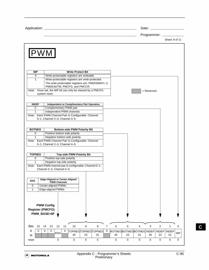
�Appendix C - Programmer’s Sheets C-95
Preliminary
Application: Date:
Programmer:Sheet
C
PWM
9 of 11
Bits 15 14 13 12 11 10 9 8 7 6 5 4 3 2 1 0
R 0 0 0EDG
0 TOPNEG45
TOPNEG23
TOPNEG01
0 BOTNEG45
BOTNEG23
BOTNEG01
INDEP45
INDEP23
INDEP01
WPW
reset 0 0 0 0 0 0 0 0 0 0 0
EDG Edge-Aligned or Center-Aligned PWM Channels
0 Center-aligned PWMs1 Edge-aligned PWMs
PWM ConfigRegister (PMCFG)
PWM_BASE+$F
TOPNEG Top-side PWM Polarity Bit0 Positive top-side polarity1 Negative top-side polarity
Note: Each PWM channel pair is configurable: Channel 0–1, Channel 2–3, Channel 4–5.
BOTNEG Bottom-side PWM Polarity Bit0 Positive bottom-side polarity1 Negative bottom-side polarity
Note: Each PWM Channel Pair Is Configurable: Channel 0–1, Channel 2–3, Channel 4–5.
INDEP Independent or Complimentary Pair Operation
0 Complementary PWM pair1 Independent PWM channels
Note: Each PWM Channel Pair Is Configurable: Channel 0–1, Channel 2–3, Channel 4–5.
WP Write Protect Bit 0 Write-protectable registers are writeable1 Write-protectable registers are write-protected
The write protectable registers are: PMDISMAP1–2, PMDEADTM, PMCFG, and PMCCR.
Note: Once set, the WP bit can only be cleared by a PMCFG system reset.
= Reserved
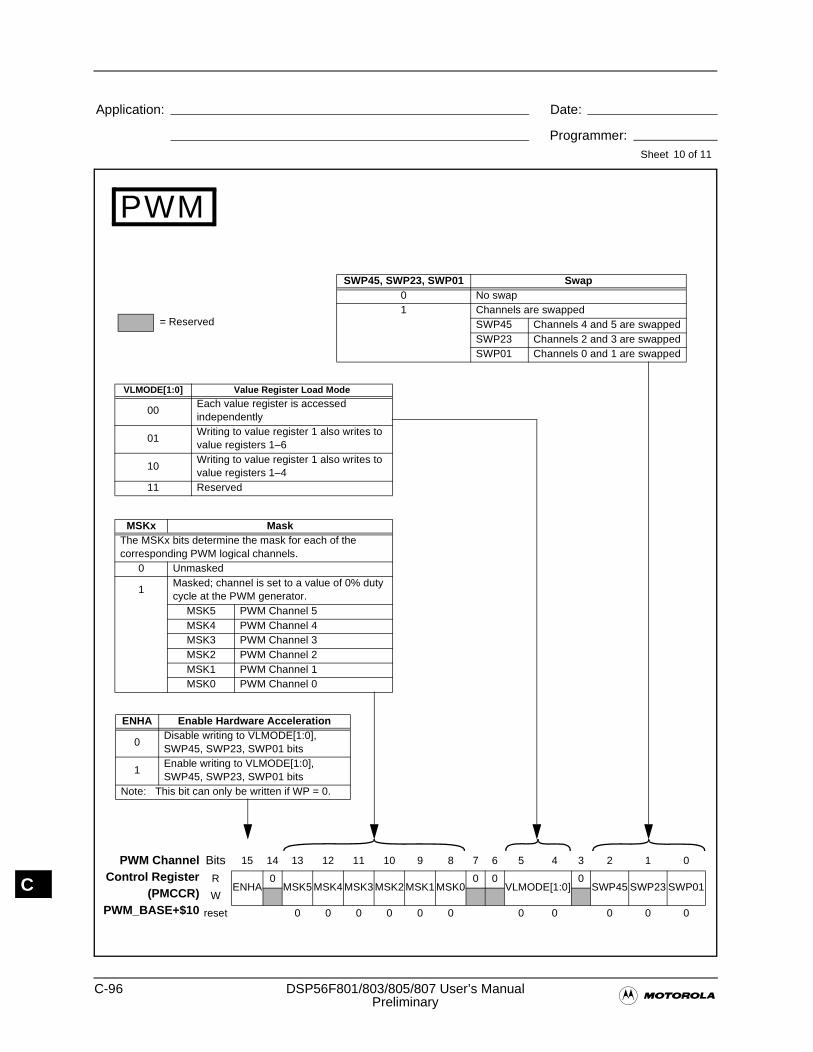
C-96 DSP56F801/803/805/807 User’s Manual�Preliminary
Application: Date:
Programmer:Sheet
C
PWM
10 of 11
PWM ChannelControl Register
(PMCCR)PWM_BASE+$10
Bits 15 14 13 12 11 10 9 8 7 6 5 4 3 2 1 0
RENHA
0MSK5 MSK4 MSK3 MSK2 MSK1 MSK0
0 0VLMODE[1:0]
0SWP45 SWP23 SWP01
W
reset 0 0 0 0 0 0 0 0 0 0 0
ENHA Enable Hardware Acceleration
0Disable writing to VLMODE[1:0], SWP45, SWP23, SWP01 bits
1Enable writing to VLMODE[1:0], SWP45, SWP23, SWP01 bits
Note: This bit can only be written if WP = 0.
MSKx Mask The MSKx bits determine the mask for each of the corresponding PWM logical channels.
0 Unmasked
1Masked; channel is set to a value of 0% duty cycle at the PWM generator.
MSK5 PWM Channel 5MSK4 PWM Channel 4MSK3 PWM Channel 3MSK2 PWM Channel 2MSK1 PWM Channel 1MSK0 PWM Channel 0
VLMODE[1:0] Value Register Load Mode
00Each value register is accessed independently
01Writing to value register 1 also writes to value registers 1–6
10Writing to value register 1 also writes to value registers 1–4
11 Reserved
SWP45, SWP23, SWP01 Swap0 No swap1 Channels are swapped
SWP45 Channels 4 and 5 are swappedSWP23 Channels 2 and 3 are swappedSWP01 Channels 0 and 1 are swapped
= Reserved
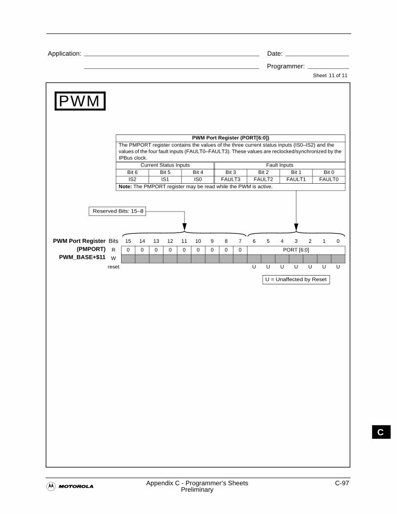
�Appendix C - Programmer’s Sheets C-97
Preliminary
Application: Date:
Programmer:Sheet
C
PWM
11 of 11
PWM Port Register(PMPORT)
PWM_BASE+$11
Bits 15 14 13 12 11 10 9 8 7 6 5 4 3 2 1 0
R 0 0 0 0 0 0 0 0 0 PORT [6:0]
W
reset U U U U U U U
PWM Port Register (PORT[6:0])The PMPORT register contains the values of the three current status inputs (IS0–IS2) and the values of the four fault inputs (FAULT0–FAULT3). These values are reclocked/synchronized by the IPBus clock.
Current Status Inputs Fault InputsBit 6 Bit 5 Bit 4 Bit 3 Bit 2 Bit 1 Bit 0IS2 IS1 IS0 FAULT3 FAULT2 FAULT1 FAULT0
Note: The PMPORT register may be read while the PWM is active.
Reserved Bits: 15–8
U = Unaffected by Reset
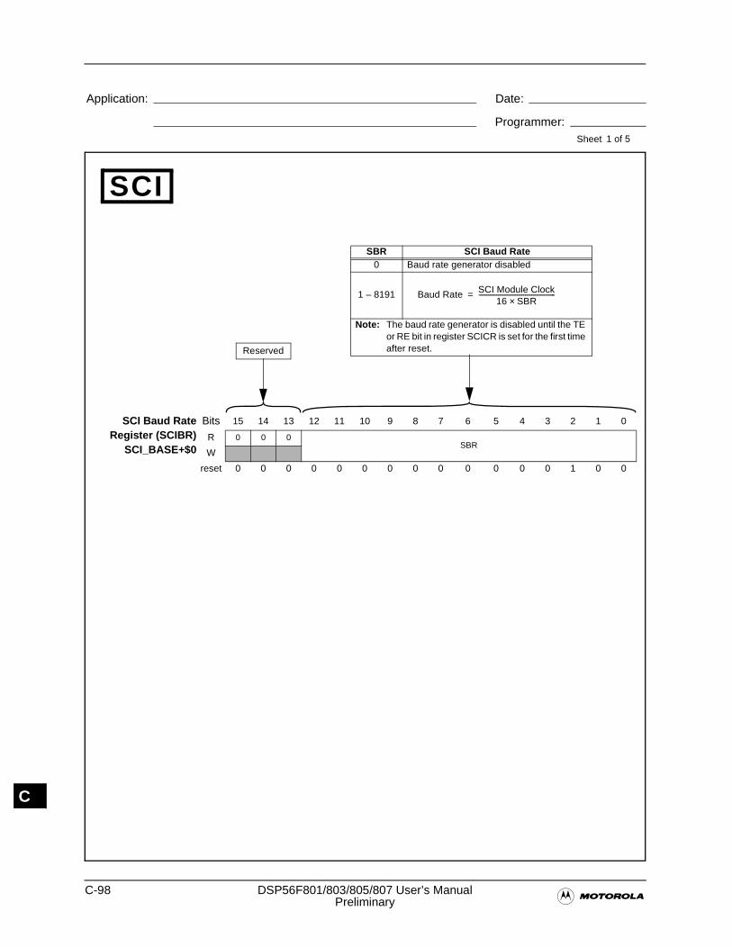
C-98 DSP56F801/803/805/807 User’s Manual�Preliminary
Application: Date:
Programmer:Sheet
C
SBR SCI Baud Rate0 Baud rate generator disabled
1 – 8191
Note: The baud rate generator is disabled until the TE or RE bit in register SCICR is set for the first time after reset.
Baud Rate SCI Module Clock16 SBR×
------------------------------------------------=
SCI Baud RateRegister (SCIBR)
SCI_BASE+$0
Bits 15 14 13 12 11 10 9 8 7 6 5 4 3 2 1 0
R 0 0 0SBR
W
reset 0 0 0 0 0 0 0 0 0 0 0 0 0 1 0 0
SCI
1 of 5
Reserved
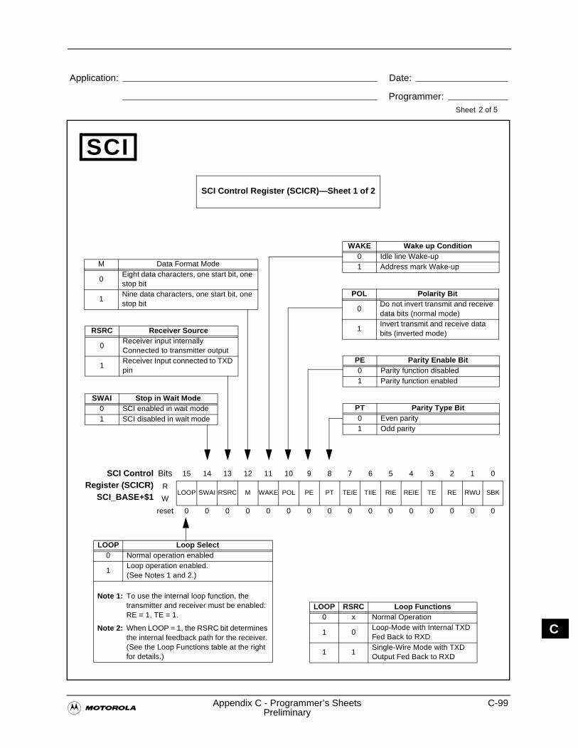
�Appendix C - Programmer’s Sheets C-99
Preliminary
Application: Date:
Programmer:Sheet
C
SCI
2 of 5
PT Parity Type Bit0 Even parity1 Odd parity
SWAI Stop in Wait Mode0 SCI enabled in wait mode1 SCI disabled in wait mode
RSRC Receiver Source
0Receiver input internally Connected to transmitter output
1Receiver Input connected to TXD pin
M Data Format Mode
0Eight data characters, one start bit, one stop bit
1Nine data characters, one start bit, one stop bit
SCI ControlRegister (SCICR)
SCI_BASE+$1
Bits 15 14 13 12 11 10 9 8 7 6 5 4 3 2 1 0
RLOOP SWAI RSRC M WAKE POL PE PT TEIE TIIE RIE REIE TE RE RWU SBK
W
reset 0 0 0 0 0 0 0 0 0 0 0 0 0 0 0 0
LOOP Loop Select0 Normal operation enabled
1Loop operation enabled. (See Notes 1 and 2.)
Note 1: To use the internal loop function, the transmitter and receiver must be enabled: RE = 1, TE = 1.
Note 2: When LOOP = 1, the RSRC bit determines the internal feedback path for the receiver. (See the Loop Functions table at the right for details.)
PE Parity Enable Bit0 Parity function disabled1 Parity function enabled
POL Polarity Bit
0Do not invert transmit and receive data bits (normal mode)
1Invert transmit and receive data bits (inverted mode)
WAKE Wake up Condition0 Idle line Wake-up1 Address mark Wake-up
SCI Control Register (SCICR)—Sheet 1 of 2
LOOP RSRC Loop Functions0 x Normal Operation
1 0Loop-Mode with Internal TXD Fed Back to RXD
1 1Single-Wire Mode with TXD Output Fed Back to RXD

C-100 DSP56F801/803/805/807 User’s Manual�Preliminary
Application: Date:
Programmer:Sheet
C
RWU Receiver Wake-up0 Normal operation1 Transmit break characters
TEIE Transmitter Empty Interrupt Enable0 TDRE interrupt requests disabled1 TDRE interrupt requests enabled
TIIE Transmitter Idle Interrupt Enable0 TI interrupt requests disabled1 TI interrupt requests enabled
RIE Receive Full Interrupt Enable0 RDRF and OR interrupt requests disabled1 RDRF and OR interrupt requests enabled
SCI ControlRegister (SCICR)
SCI_BASE+$1
Bits 15 14 13 12 11 10 9 8 7 6 5 4 3 2 1 0
RLOOP SWAI RSRC M WAKE POL PE PT TEIE TIIE RIE REIE TE RE RWU SBK
W
reset 0 0 0 0 0 0 0 0 0 0 0 0 0 0 0 0
REIE Receive Error Interrupt Enable0 Error interrupt requests disabled1 Error interrupt requests enabled
TE Transmitter Enable
0Transmitter disabled—TXD pin is in high-impedance state
1 Transmitter enabled
RE Receiver Enable0 Receiver disabled1 Receiver enabled
SBK Send Break0 No break characters transmitted1 Transmit break characters
SCI Control Register (SCICR)—Sheet 2 of 2
SCI
3 of 5
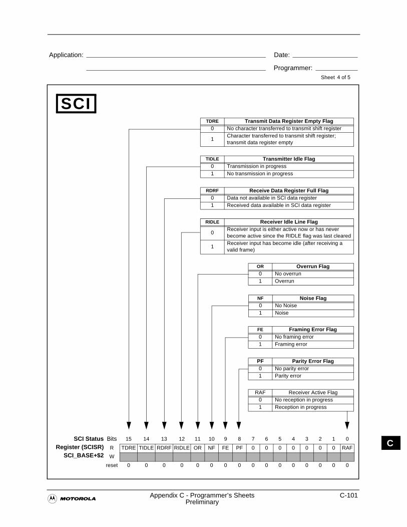
�Appendix C - Programmer’s Sheets C-101
Preliminary
Application: Date:
Programmer:Sheet
C
TIDLE Transmitter Idle Flag0 Transmission in progress1 No transmission in progress
PF Parity Error Flag0 No parity error1 Parity error
FE Framing Error Flag0 No framing error1 Framing error
NF Noise Flag0 No Noise1 Noise
SCI StatusRegister (SCISR)
SCI_BASE+$2
Bits 15 14 13 12 11 10 9 8 7 6 5 4 3 2 1 0
R TDRE TIDLE RDRF RIDLE OR NF FE PF 0 0 0 0 0 0 0 RAF
W
reset 0 0 0 0 0 0 0 0 0 0 0 0 0 0 0 0
OR Overrun Flag0 No overrun1 Overrun
RIDLE Receiver Idle Line Flag
0Receiver input is either active now or has never become active since the RIDLE flag was last cleared
1Receiver input has become idle (after receiving a valid frame)
RDRF Receive Data Register Full Flag0 Data not available in SCI data register1 Received data available in SCI data register
TDRE Transmit Data Register Empty Flag0 No character transferred to transmit shift register
1Character transferred to transmit shift register; transmit data register empty
SCI
4 of 5
RAF Receiver Active Flag0 No reception in progress1 Reception in progress
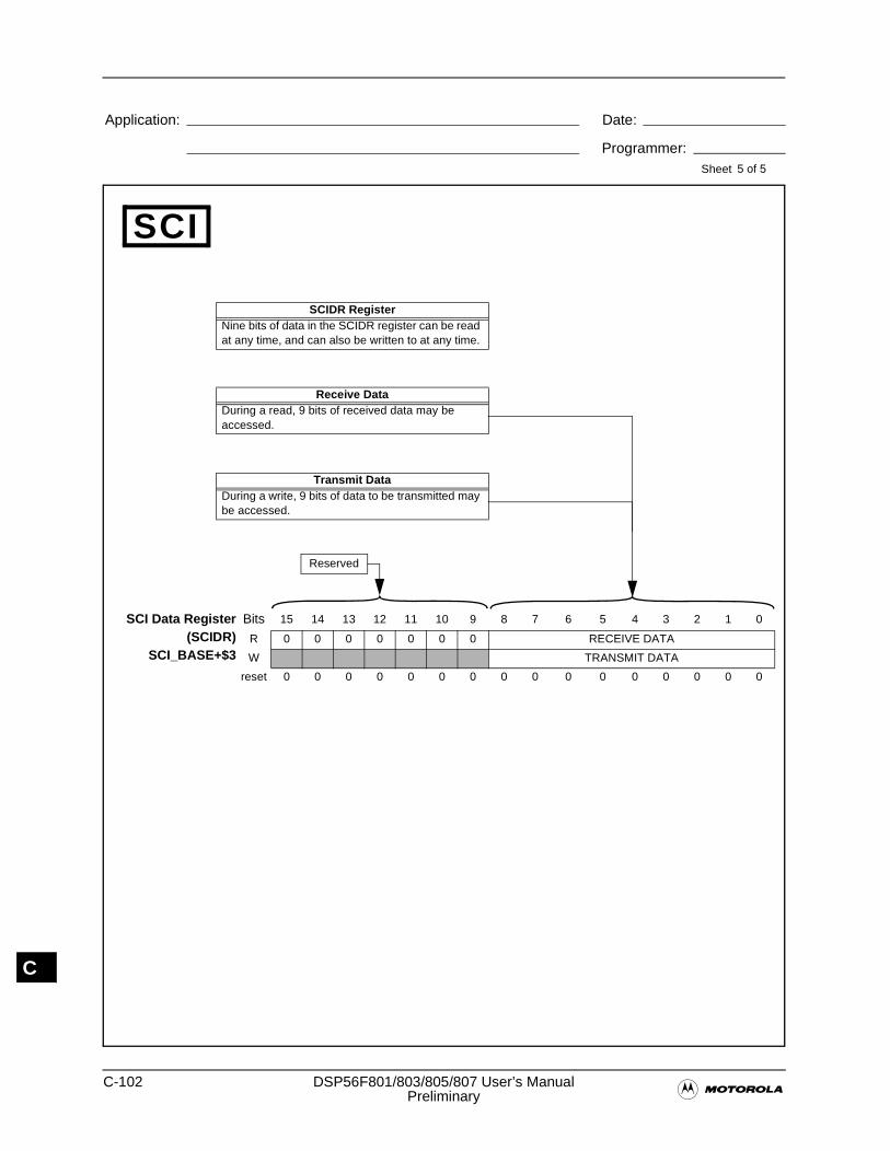
C-102 DSP56F801/803/805/807 User’s Manual�Preliminary
Application: Date:
Programmer:Sheet
C
Receive DataDuring a read, 9 bits of received data may be accessed.
SCI Data Register(SCIDR)
SCI_BASE+$3
Bits 15 14 13 12 11 10 9 8 7 6 5 4 3 2 1 0
R 0 0 0 0 0 0 0 RECEIVE DATA
W TRANSMIT DATA
reset 0 0 0 0 0 0 0 0 0 0 0 0 0 0 0 0
SCI
5 of 5
Transmit DataDuring a write, 9 bits of data to be transmitted may be accessed.
SCIDR RegisterNine bits of data in the SCIDR register can be read at any time, and can also be written to at any time.
Reserved
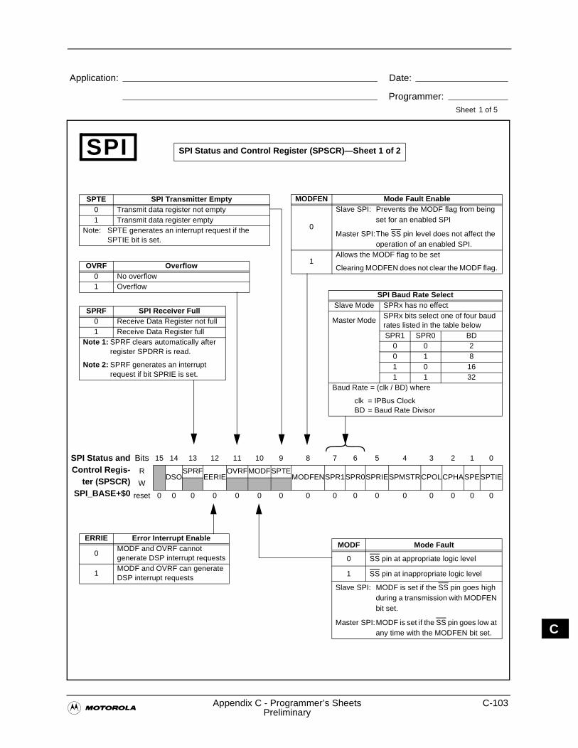
�Appendix C - Programmer’s Sheets C-103
Preliminary
Application: Date:
Programmer:Sheet
C
MODF Mode Fault
0 SS pin at appropriate logic level
1 SS pin at inappropriate logic level
Slave SPI: MODF is set if the SS pin goes high during a transmission with MODFEN bit set.
Master SPI:MODF is set if the SS pin goes low at any time with the MODFEN bit set.
ERRIE Error Interrupt Enable
0MODF and OVRF cannot generate DSP interrupt requests
1MODF and OVRF can generate DSP interrupt requests
SPI Status andControl Regis-
ter (SPSCR)SPI_BASE+$0
Bits 15 14 13 12 11 10 9 8 7 6 5 4 3 2 1 0
RDSO
SPRFEERIE
OVRFMODFSPTEMODFENSPR1SPR0SPRIESPMSTRCPOLCPHASPESPTIE
W
reset 0 0 0 0 0 0 0 0 0 0 0 0 0 0 0 0
MODFEN Mode Fault Enable
0
Slave SPI: Prevents the MODF flag from being set for an enabled SPI
Master SPI:The SS pin level does not affect the operation of an enabled SPI.
1Allows the MODF flag to be set
Clearing MODFEN does not clear the MODF flag.
SPTE SPI Transmitter Empty0 Transmit data register not empty1 Transmit data register empty
Note: SPTE generates an interrupt request if the SPTIE bit is set.
OVRF Overflow0 No overflow1 Overflow
SPI
1 of 5
SPRF SPI Receiver Full0 Receive Data Register not full1 Receive Data Register full
Note 1: SPRF clears automatically after register SPDRR is read.
Note 2: SPRF generates an interrupt request if bit SPRIE is set.
SPI Baud Rate SelectSlave Mode SPRx has no effect
Master ModeSPRx bits select one of four baud rates listed in the table belowSPR1 SPR0 BD
0 0 20 1 81 0 161 1 32
Baud Rate = (clk / BD) where
clk = IPBus ClockBD = Baud Rate Divisor
SPI Status and Control Register (SPSCR)—Sheet 1 of 2
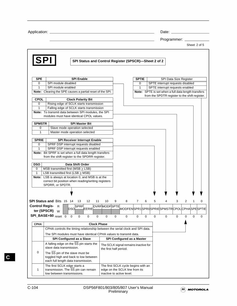
C-104 DSP56F801/803/805/807 User’s Manual�Preliminary
Application: Date:
Programmer:Sheet
C
CPOL Clock Polarity Bit0 Rising edge of SCLK starts transmission1 Falling edge of SCLK starts transmission
Note: To transmit data between SPI modules, the SPI modules must have identical CPOL values.
SPI Status andControl Regis-
ter (SPSCR)SPI_BASE+$0
Bits 15 14 13 12 11 10 9 8 7 6 5 4 3 2 1 0
RDSO
SPRFEERIE
OVRFMODFSPTEMODFENSPR1SPR0SPRIESPMSTRCPOLCPHASPESPTIE
W
reset 0 0 0 0 0 0 0 0 0 0 0 0 0 0 0 0
SPRIE SPI Receiver Interrupt Enable0 SPRF DSP interrupt requests disabled1 SPRF DSP interrupt requests enabled
Note: Bit SPRF is set when a full data length transfers from the shift register to the SPDRR register.
SPE SPI Enable0 SPI module disabled1 SPI module enabled
Note: Clearing the SPE causes a partial reset of the SPI.
SPTIE SPI Data Size Register0 SPTE interrupt requests disabled1 SPTE interrupt requests enabled
Note: SPTE is set when a full data length transfers from the SPDTR register to the shift register.
SPMSTR SPI Master Bit0 Slave mode operation selected1 Master mode operation selected
CPHA Clock Phase
CPHA controls the timing relationship between the serial clock and SPI data.
The SPI modules must have identical CPHA values to transmit data.
SPI Configured as a Slave SPI Configured as a Master
0
A falling edge on the SS pin starts the slave data transmission.
The SS pin of the slave must be toggled high and back to low between each full length data transmission.
The SCLK signal remains inactive for the first half period.
1The first SCLK edge starts a transmission. The SS pin can remain low between transmissions.
The first SCLK cycle begins with an edge on the SCLK line from its inactive to active level.
SPI Status and Control Register (SPSCR)—Sheet 2 of 2SPI
2 of 5
DSO Data Shift Order0 MSB transmitted first (MSB > LSB)1 LSB transmitted first (LSB > MSB)
Note: LSB is always at location 0, and MSB is at the correct bit position when reading/writing registers SPDRR, or SPDTR.
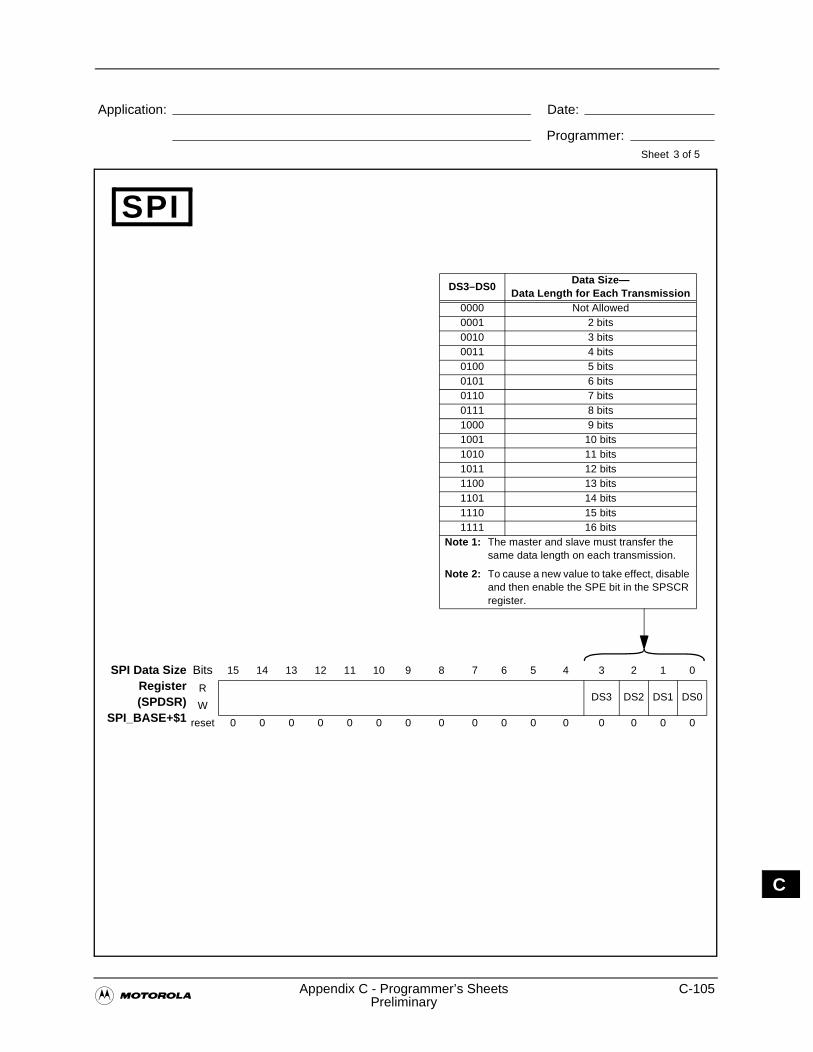
�Appendix C - Programmer’s Sheets C-105
Preliminary
Application: Date:
Programmer:Sheet
C
SPI
3 of 5
DS3–DS0Data Size—
Data Length for Each Transmission0000 Not Allowed0001 2 bits0010 3 bits0011 4 bits0100 5 bits0101 6 bits0110 7 bits0111 8 bits1000 9 bits1001 10 bits1010 11 bits1011 12 bits1100 13 bits1101 14 bits1110 15 bits1111 16 bits
Note 1: The master and slave must transfer the same data length on each transmission.
Note 2: To cause a new value to take effect, disable and then enable the SPE bit in the SPSCR register.
SPI Data SizeRegister(SPDSR)
SPI_BASE+$1
Bits 15 14 13 12 11 10 9 8 7 6 5 4 3 2 1 0
RDS3 DS2 DS1 DS0
W
reset 0 0 0 0 0 0 0 0 0 0 0 0 0 0 0 0
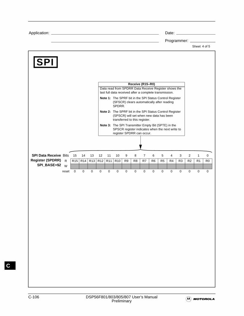
C-106 DSP56F801/803/805/807 User’s Manual�Preliminary
Application: Date:
Programmer:Sheet
C
Receive (R15–R0)Data read from SPDRR Data Receive Register shows the last full data received after a complete transmission.
Note 1: The SPRF bit in the SPI Status Control Register (SFSCR) clears automatically after reading SPDRR.
Note 2: The SPRF bit in the SPI Status Control Register (SPSCR) will set when new data has been transferred to this register.
Note 3: The SPI Transmitter Empty Bit (SPTE) in the SPSCR register indicates when the next write to register SPDRR can occur.
SPI
4 of 5
SPI Data ReceiveRegister (SPDRR)
SPI_BASE+$2
Bits 15 14 13 12 11 10 9 8 7 6 5 4 3 2 1 0
R R15 R14 R13 R12 R11 R10 R9 R8 R7 R6 R5 R4 R3 R2 R1 R0
W
reset 0 0 0 0 0 0 0 0 0 0 0 0 0 0 0 0
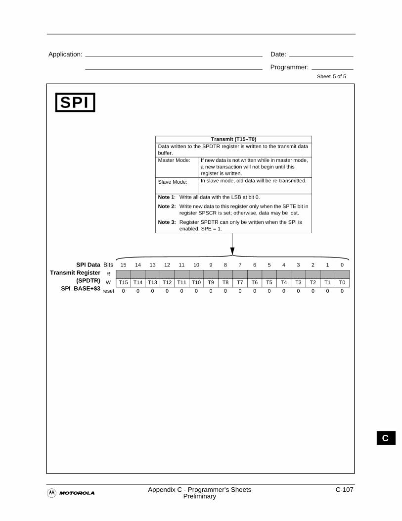
�Appendix C - Programmer’s Sheets C-107
Preliminary
Application: Date:
Programmer:Sheet
C
Transmit (T15–T0)Data written to the SPDTR register is written to the transmit data buffer. Master Mode: If new data is not written while in master mode,
a new transaction will not begin until this register is written.
Slave Mode: In slave mode, old data will be re-transmitted.
Note 1 : Write all data with the LSB at bit 0.
Note 2: Write new data to this register only when the SPTE bit in register SPSCR is set; otherwise, data may be lost.
Note 3: Register SPDTR can only be written when the SPI is enabled, SPE = 1.
SPI
5 of 5
SPI DataTransmit Register
(SPDTR)SPI_BASE+$3
Bits 15 14 13 12 11 10 9 8 7 6 5 4 3 2 1 0
R
W T15 T14 T13 T12 T11 T10 T9 T8 T7 T6 T5 T4 T3 T2 T1 T0
reset 0 0 0 0 0 0 0 0 0 0 0 0 0 0 0 0
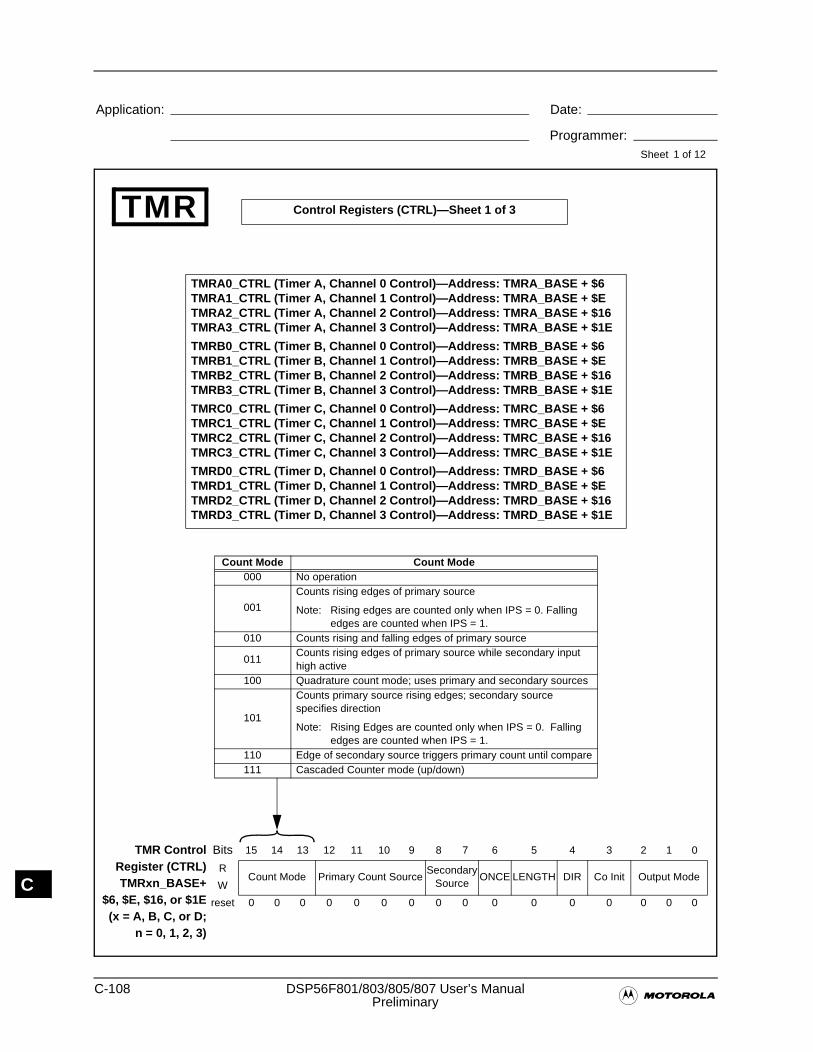
C-108 DSP56F801/803/805/807 User’s Manual�Preliminary
Application: Date:
Programmer:Sheet
C
TMR ControlRegister (CTRL)TMRxn_BASE+
$6, $E, $16, or $1E(x = A, B, C, or D;
n = 0, 1, 2, 3)
Bits 15 14 13 12 11 10 9 8 7 6 5 4 3 2 1 0
RCount Mode Primary Count Source
Secondary Source
ONCE LENGTH DIR Co Init Output ModeW
reset 0 0 0 0 0 0 0 0 0 0 0 0 0 0 0 0
TMRA0_CTRL (Timer A, Channel 0 Control)—Address: TMRA_BASE + $6TMRA1_CTRL (Timer A, Channel 1 Control)—Address: TMRA_BASE + $ETMRA2_CTRL (Timer A, Channel 2 Control)—Address: TMRA_BASE + $16TMRA3_CTRL (Timer A, Channel 3 Control)—Address: TMRA_BASE + $1E
TMRB0_CTRL (Timer B, Channel 0 Control)—Address: TMRB_BASE + $6TMRB1_CTRL (Timer B, Channel 1 Control)—Address: TMRB_BASE + $ETMRB2_CTRL (Timer B, Channel 2 Control)—Address: TMRB_BASE + $16TMRB3_CTRL (Timer B, Channel 3 Control)—Address: TMRB_BASE + $1E
TMRC0_CTRL (Timer C, Channel 0 Control)—Address: TMRC_BASE + $6TMRC1_CTRL (Timer C, Channel 1 Control)—Address: TMRC_BASE + $ETMRC2_CTRL (Timer C, Channel 2 Control)—Address: TMRC_BASE + $16TMRC3_CTRL (Timer C, Channel 3 Control)—Address: TMRC_BASE + $1E
TMRD0_CTRL (Timer D, Channel 0 Control)—Address: TMRD_BASE + $6TMRD1_CTRL (Timer D, Channel 1 Control)—Address: TMRD_BASE + $ETMRD2_CTRL (Timer D, Channel 2 Control)—Address: TMRD_BASE + $16TMRD3_CTRL (Timer D, Channel 3 Control)—Address: TMRD_BASE + $1E
Control Registers (CTRL)—Sheet 1 of 3TMR
1 of 12
Count Mode Count Mode000 No operation
001
Counts rising edges of primary source
Note: Rising edges are counted only when IPS = 0. Falling edges are counted when IPS = 1.
010 Counts rising and falling edges of primary source
011Counts rising edges of primary source while secondary input high active
100 Quadrature count mode; uses primary and secondary sources
101
Counts primary source rising edges; secondary source specifies direction
Note: Rising Edges are counted only when IPS = 0. Falling edges are counted when IPS = 1.
110 Edge of secondary source triggers primary count until compare111 Cascaded Counter mode (up/down)
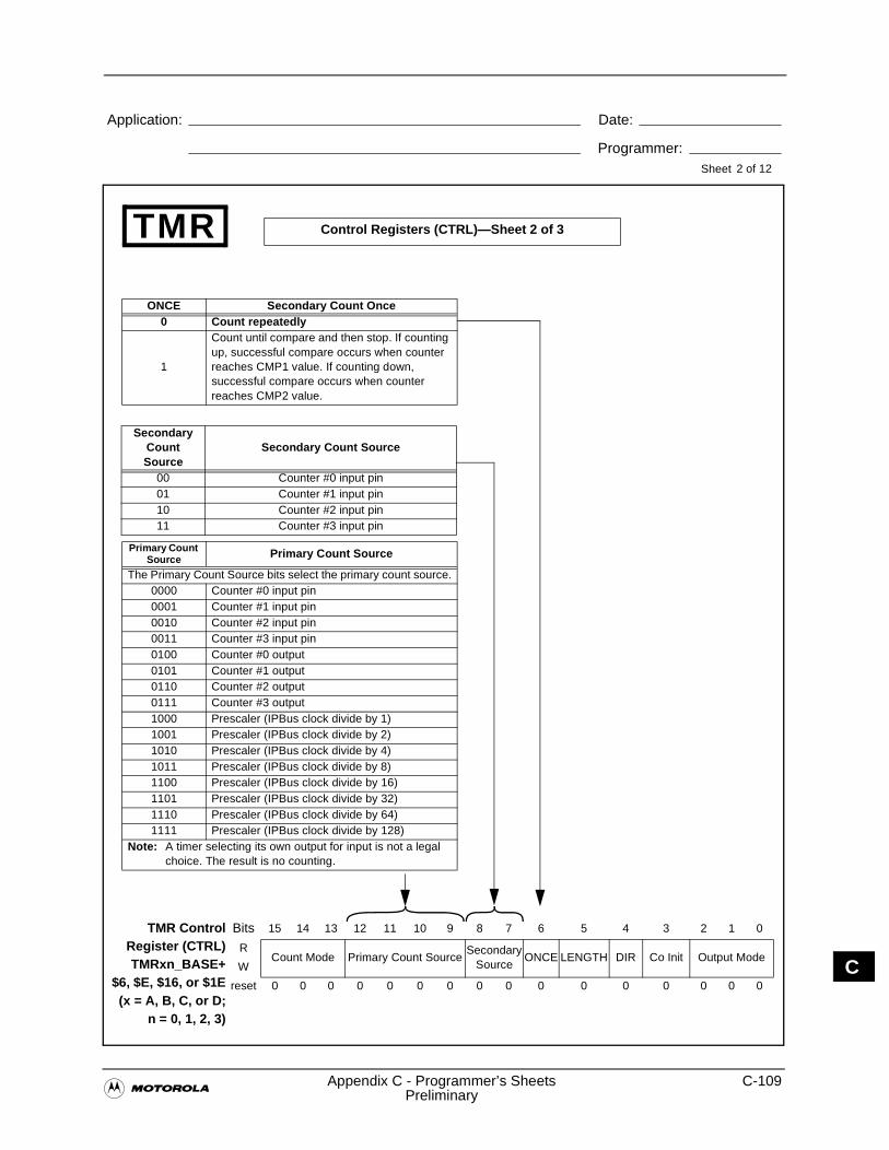
�Appendix C - Programmer’s Sheets C-109
Preliminary
Application: Date:
Programmer:Sheet
C
TMR ControlRegister (CTRL)TMRxn_BASE+
$6, $E, $16, or $1E(x = A, B, C, or D;
n = 0, 1, 2, 3)
Bits 15 14 13 12 11 10 9 8 7 6 5 4 3 2 1 0
RCount Mode Primary Count Source
Secondary Source
ONCE LENGTH DIR Co Init Output ModeW
reset 0 0 0 0 0 0 0 0 0 0 0 0 0 0 0 0
Control Registers (CTRL)—Sheet 2 of 3TMR
2 of 12
Secondary Count Source
Secondary Count Source
00 Counter #0 input pin01 Counter #1 input pin10 Counter #2 input pin11 Counter #3 input pin
ONCE Secondary Count Once0 Count repeatedly
1
Count until compare and then stop. If counting up, successful compare occurs when counter reaches CMP1 value. If counting down, successful compare occurs when counter reaches CMP2 value.
Primary Count Source Primary Count Source
The Primary Count Source bits select the primary count source.0000 Counter #0 input pin0001 Counter #1 input pin0010 Counter #2 input pin0011 Counter #3 input pin0100 Counter #0 output0101 Counter #1 output0110 Counter #2 output0111 Counter #3 output1000 Prescaler (IPBus clock divide by 1)1001 Prescaler (IPBus clock divide by 2)1010 Prescaler (IPBus clock divide by 4)1011 Prescaler (IPBus clock divide by 8)1100 Prescaler (IPBus clock divide by 16)1101 Prescaler (IPBus clock divide by 32)1110 Prescaler (IPBus clock divide by 64)1111 Prescaler (IPBus clock divide by 128)
Note: A timer selecting its own output for input is not a legal choice. The result is no counting.
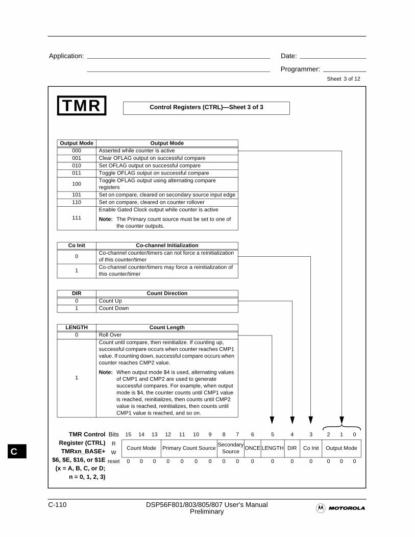
C-110 DSP56F801/803/805/807 User’s Manual�Preliminary
Application: Date:
Programmer:Sheet
C
LENGTH Count Length0 Roll Over
1
Count until compare, then reinitialize. If counting up, successful compare occurs when counter reaches CMP1 value. If counting down, successful compare occurs when counter reaches CMP2 value.
Note: When output mode $4 is used, alternating values of CMP1 and CMP2 are used to generate successful compares. For example, when output mode is $4, the counter counts until CMP1 value is reached, reinitializes, then counts until CMP2 value is reached, reinitializes, then counts until CMP1 value is reached, and so on.
DIR Count Direction0 Count Up1 Count Down
Co Init Co-channel Initialization
0Co-channel counter/timers can not force a reinitialization of this counter/timer
1Co-channel counter/timers may force a reinitialization of this counter/timer
Control Registers (CTRL)—Sheet 3 of 3TMR
3 of 12
Output Mode Output Mode000 Asserted while counter is active001 Clear OFLAG output on successful compare010 Set OFLAG output on successful compare011 Toggle OFLAG output on successful compare
100Toggle OFLAG output using alternating compare registers
101 Set on compare, cleared on secondary source input edge110 Set on compare, cleared on counter rollover
111
Enable Gated Clock output while counter is active
Note: The Primary count source must be set to one of the counter outputs.
TMR ControlRegister (CTRL)TMRxn_BASE+
$6, $E, $16, or $1E(x = A, B, C, or D;
n = 0, 1, 2, 3)
Bits 15 14 13 12 11 10 9 8 7 6 5 4 3 2 1 0
RCount Mode Primary Count Source
Secondary Source
ONCE LENGTH DIR Co Init Output ModeW
reset 0 0 0 0 0 0 0 0 0 0 0 0 0 0 0 0
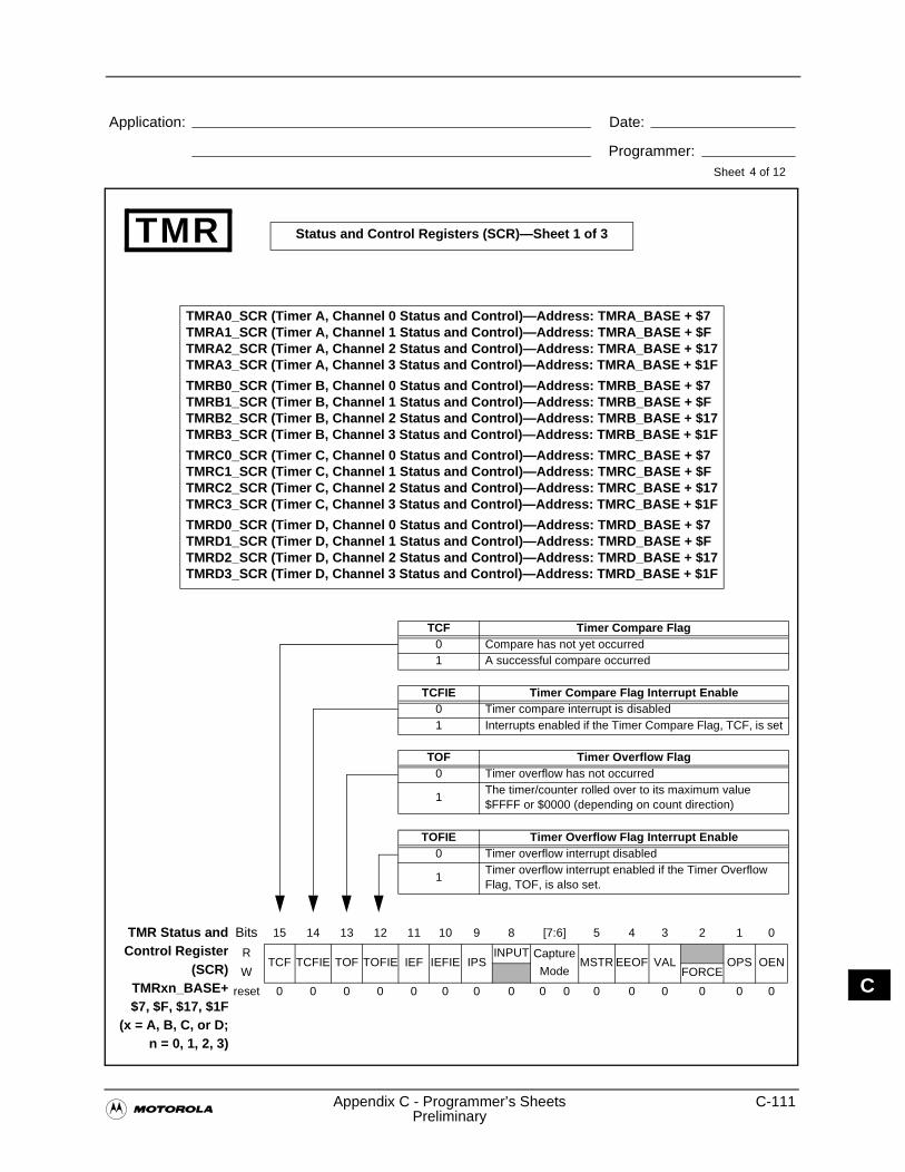
�Appendix C - Programmer’s Sheets C-111
Preliminary
Application: Date:
Programmer:Sheet
C
TMR
4 of 12
TMRA0_SCR (Timer A, Channel 0 Status and Control)—Address: TMRA_BASE + $7TMRA1_SCR (Timer A, Channel 1 Status and Control)—Address: TMRA_BASE + $FTMRA2_SCR (Timer A, Channel 2 Status and Control)—Address: TMRA_BASE + $17TMRA3_SCR (Timer A, Channel 3 Status and Control)—Address: TMRA_BASE + $1F
TMRB0_SCR (Timer B, Channel 0 Status and Control)—Address: TMRB_BASE + $7TMRB1_SCR (Timer B, Channel 1 Status and Control)—Address: TMRB_BASE + $FTMRB2_SCR (Timer B, Channel 2 Status and Control)—Address: TMRB_BASE + $17TMRB3_SCR (Timer B, Channel 3 Status and Control)—Address: TMRB_BASE + $1F
TMRC0_SCR (Timer C, Channel 0 Status and Control)—Address: TMRC_BASE + $7TMRC1_SCR (Timer C, Channel 1 Status and Control)—Address: TMRC_BASE + $FTMRC2_SCR (Timer C, Channel 2 Status and Control)—Address: TMRC_BASE + $17TMRC3_SCR (Timer C, Channel 3 Status and Control)—Address: TMRC_BASE + $1F
TMRD0_SCR (Timer D, Channel 0 Status and Control)—Address: TMRD_BASE + $7TMRD1_SCR (Timer D, Channel 1 Status and Control)—Address: TMRD_BASE + $FTMRD2_SCR (Timer D, Channel 2 Status and Control)—Address: TMRD_BASE + $17TMRD3_SCR (Timer D, Channel 3 Status and Control)—Address: TMRD_BASE + $1F
TCFIE Timer Compare Flag Interrupt Enable0 Timer compare interrupt is disabled1 Interrupts enabled if the Timer Compare Flag, TCF, is set
TCF Timer Compare Flag0 Compare has not yet occurred1 A successful compare occurred
TOF Timer Overflow Flag 0 Timer overflow has not occurred
1The timer/counter rolled over to its maximum value $FFFF or $0000 (depending on count direction)
TMR Status andControl Register
(SCR)TMRxn_BASE+$7, $F, $17, $1F
(x = A, B, C, or D;n = 0, 1, 2, 3)
Bits 15 14 13 12 11 10 9 8 [7:6] 5 4 3 2 1 0
RTCF TCFIE TOF TOFIE IEF IEFIE IPS
INPUT Capture
ModeMSTR EEOF VAL OPS OEN
W FORCE
reset 0 0 0 0 0 0 0 0 0 0 0 0 0 0 0 0
TOFIE Timer Overflow Flag Interrupt Enable0 Timer overflow interrupt disabled
1Timer overflow interrupt enabled if the Timer Overflow Flag, TOF, is also set.
Status and Control Registers (SCR)—Sheet 1 of 3
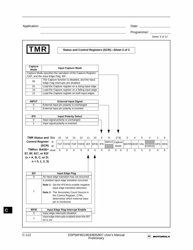
C-112 DSP56F801/803/805/807 User’s Manual�Preliminary
Application: Date:
Programmer:Sheet
C
TMR
5 of 12
Status and Control Registers (SCR)—Sheet 2 of 3
IEF Input Edge Flag0 An input edge transition has not occurred
1
A positive input edge transition occurred
Note 1: Set the IPS bit to enable negative input edge transition detection.
Note 2: The Secondary Count Source in the Control Register, CTRL, determines which external input pin is monitored.
IEFIE Input Edge Flag Interrupt Enable0 Input edge interrupts disabled
1Input edge interrupts enabled when the IEF bit is set
IPS Input Polarity Select 0 Input signal polarity is unchanged1 Input signal polarity is inverted
Capture Mode
Input Capture Mode
Capture Mode specifies the operation of the Capture Register, CAP, and the Input Edge Flag, IEF.
00The Capture function is disabled, and the Input Edge Flag interrupts are disabled
01 Load the Capture register on a rising input edge10 Load the Capture register on a falling input edge11 Load the Capture register on both input edges
INPUT External Input Signal0 External input pin polarity is unchanged1 External input pin polarity is inverted
TMR Status andControl Register
(SCR)TMRxn_BASE+
$7, $F, $17, or $1F(x = A, B, C, or D;
n = 0, 1, 2, 3)
Bits 15 14 13 12 11 10 9 8 [7:6] 5 4 3 2 1 0
RTCF TCFIE TOF TOFIE IEF IEFIE IPS
INPUT Capture
ModeMSTR EEOF VAL OPS OEN
W FORCE
reset 0 0 0 0 0 0 0 0 0 0 0 0 0 0 0 0
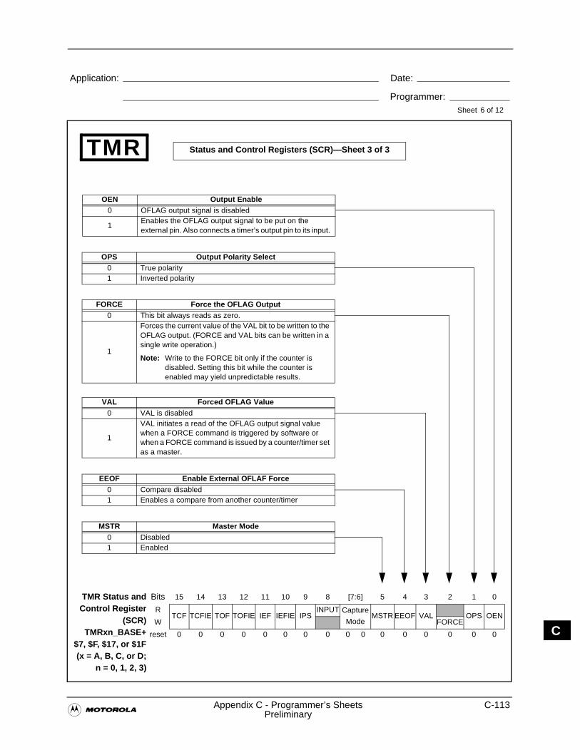
�Appendix C - Programmer’s Sheets C-113
Preliminary
Application: Date:
Programmer:Sheet
C
TMR
6 of 12
VAL Forced OFLAG Value 0 VAL is disabled
1
VAL initiates a read of the OFLAG output signal value when a FORCE command is triggered by software or when a FORCE command is issued by a counter/timer set as a master.
FORCE Force the OFLAG Output0 This bit always reads as zero.
1
Forces the current value of the VAL bit to be written to the OFLAG output. (FORCE and VAL bits can be written in a single write operation.)
Note: Write to the FORCE bit only if the counter is disabled. Setting this bit while the counter is enabled may yield unpredictable results.
OPS Output Polarity Select0 True polarity1 Inverted polarity
OEN Output Enable0 OFLAG output signal is disabled
1Enables the OFLAG output signal to be put on the external pin. Also connects a timer’s output pin to its input.
TMR Status andControl Register
(SCR)TMRxn_BASE+
$7, $F, $17, or $1F(x = A, B, C, or D;
n = 0, 1, 2, 3)
Bits 15 14 13 12 11 10 9 8 [7:6] 5 4 3 2 1 0
RTCF TCFIE TOF TOFIE IEF IEFIE IPS
INPUT Capture
ModeMSTR EEOF VAL OPS OEN
W FORCE
reset 0 0 0 0 0 0 0 0 0 0 0 0 0 0 0 0
MSTR Master Mode0 Disabled1 Enabled
Status and Control Registers (SCR)—Sheet 3 of 3
EEOF Enable External OFLAF Force 0 Compare disabled1 Enables a compare from another counter/timer
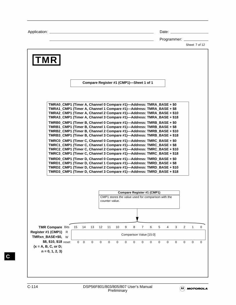
C-114 DSP56F801/803/805/807 User’s Manual�Preliminary
Application: Date:
Programmer:Sheet
C
TMR
7 of 12
TMRA0_CMP1 (Timer A, Channel 0 Compare #1)—Address: TMRA_BASE + $0TMRA1_CMP1 (Timer A, Channel 1 Compare #1)—Address: TMRA_BASE + $8TMRA2_CMP1 (Timer A, Channel 2 Compare #1)—Address: TMRA_BASE + $10TMRA3_CMP1 (Timer A, Channel 3 Compare #1)—Address: TMRA_BASE + $18
TMRB0_CMP1 (Timer B, Channel 0 Compare #1)—Address: TMRB_BASE + $0TMRB1_CMP1 (Timer B, Channel 1 Compare #1)—Address: TMRB_BASE + $8TMRB2_CMP1 (Timer B, Channel 2 Compare #1)—Address: TMRB_BASE + $10TMRB3_CMP1 (Timer B, Channel 3 Compare #1)—Address: TMRB_BASE + $18
TMRC0_CMP1 (Timer C, Channel 0 Compare #1)—Address: TMRC_BASE + $0TMRC1_CMP1 (Timer C, Channel 1 Compare #1)—Address: TMRC_BASE + $8TMRC2_CMP1 (Timer C, Channel 2 Compare #1)—Address: TMRC_BASE + $10TMRC3_CMP1 (Timer C, Channel 3 Compare #1)—Address: TMRC_BASE + $18
TMRD0_CMP1 (Timer D, Channel 0 Compare #1)—Address: TMRD_BASE + $0TMRD1_CMP1 (Timer D, Channel 1 Compare #1)—Address: TMRD_BASE + $8TMRD2_CMP1 (Timer D, Channel 2 Compare #1)—Address: TMRD_BASE + $10TMRD3_CMP1 (Timer D, Channel 3 Compare #1)—Address: TMRD_BASE + $18
Compare Register #1 (CMP1)CMP1 stores the value used for comparison with the counter value.
TMR CompareRegister #1 (CMP1)TMRxn_BASE+$0,
$8, $10, $18(x = A, B, C, or D;
n = 0, 1, 2, 3)
Bits 15 14 13 12 11 10 9 8 7 6 5 4 3 2 1 0
RComparison Value [15:0]
W
reset 0 0 0 0 0 0 0 0 0 0 0 0 0 0 0 0
Compare Register #1 (CMP1)—Sheet 1 of 1
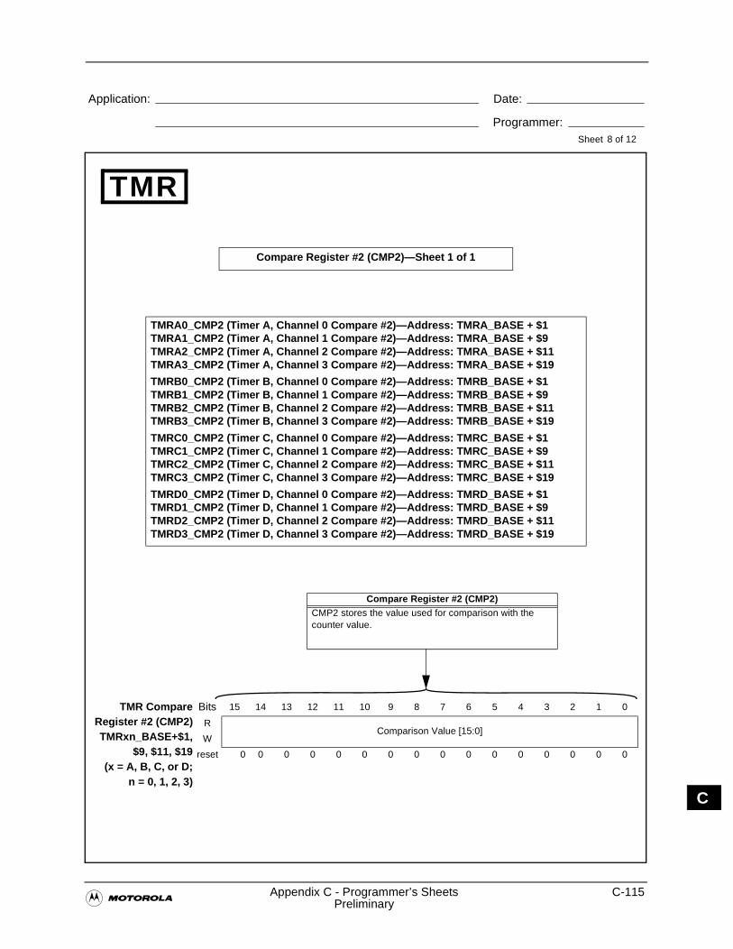
�Appendix C - Programmer’s Sheets C-115
Preliminary
Application: Date:
Programmer:Sheet
C
TMR
8 of 12
TMRA0_CMP2 (Timer A, Channel 0 Compare #2)—Address: TMRA_BASE + $1TMRA1_CMP2 (Timer A, Channel 1 Compare #2)—Address: TMRA_BASE + $9TMRA2_CMP2 (Timer A, Channel 2 Compare #2)—Address: TMRA_BASE + $11TMRA3_CMP2 (Timer A, Channel 3 Compare #2)—Address: TMRA_BASE + $19
TMRB0_CMP2 (Timer B, Channel 0 Compare #2)—Address: TMRB_BASE + $1TMRB1_CMP2 (Timer B, Channel 1 Compare #2)—Address: TMRB_BASE + $9TMRB2_CMP2 (Timer B, Channel 2 Compare #2)—Address: TMRB_BASE + $11TMRB3_CMP2 (Timer B, Channel 3 Compare #2)—Address: TMRB_BASE + $19
TMRC0_CMP2 (Timer C, Channel 0 Compare #2)—Address: TMRC_BASE + $1TMRC1_CMP2 (Timer C, Channel 1 Compare #2)—Address: TMRC_BASE + $9TMRC2_CMP2 (Timer C, Channel 2 Compare #2)—Address: TMRC_BASE + $11TMRC3_CMP2 (Timer C, Channel 3 Compare #2)—Address: TMRC_BASE + $19
TMRD0_CMP2 (Timer D, Channel 0 Compare #2)—Address: TMRD_BASE + $1TMRD1_CMP2 (Timer D, Channel 1 Compare #2)—Address: TMRD_BASE + $9TMRD2_CMP2 (Timer D, Channel 2 Compare #2)—Address: TMRD_BASE + $11TMRD3_CMP2 (Timer D, Channel 3 Compare #2)—Address: TMRD_BASE + $19
Compare Register #2 (CMP2)CMP2 stores the value used for comparison with the counter value.
TMR CompareRegister #2 (CMP2)TMRxn_BASE+$1,
$9, $11, $19(x = A, B, C, or D;
n = 0, 1, 2, 3)
Bits 15 14 13 12 11 10 9 8 7 6 5 4 3 2 1 0
RComparison Value [15:0]
W
reset 0 0 0 0 0 0 0 0 0 0 0 0 0 0 0 0
Compare Register #2 (CMP2)—Sheet 1 of 1
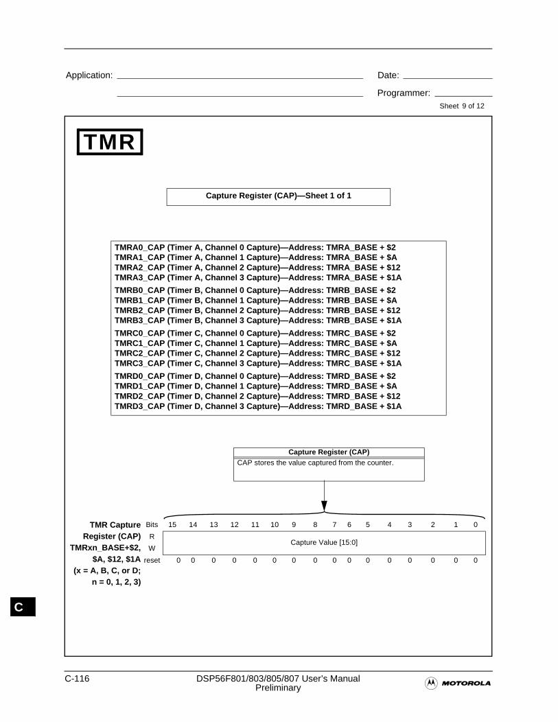
C-116 DSP56F801/803/805/807 User’s Manual�Preliminary
Application: Date:
Programmer:Sheet
C
TMR
9 of 12
TMRA0_CAP (Timer A, Channel 0 Capture)—Address: TMRA_BASE + $2TMRA1_CAP (Timer A, Channel 1 Capture)—Address: TMRA_BASE + $ATMRA2_CAP (Timer A, Channel 2 Capture)—Address: TMRA_BASE + $12TMRA3_CAP (Timer A, Channel 3 Capture)—Address: TMRA_BASE + $1A
TMRB0_CAP (Timer B, Channel 0 Capture)—Address: TMRB_BASE + $2TMRB1_CAP (Timer B, Channel 1 Capture)—Address: TMRB_BASE + $ATMRB2_CAP (Timer B, Channel 2 Capture)—Address: TMRB_BASE + $12TMRB3_CAP (Timer B, Channel 3 Capture)—Address: TMRB_BASE + $1A
TMRC0_CAP (Timer C, Channel 0 Capture)—Address: TMRC_BASE + $2TMRC1_CAP (Timer C, Channel 1 Capture)—Address: TMRC_BASE + $ATMRC2_CAP (Timer C, Channel 2 Capture)—Address: TMRC_BASE + $12TMRC3_CAP (Timer C, Channel 3 Capture)—Address: TMRC_BASE + $1A
TMRD0_CAP (Timer D, Channel 0 Capture)—Address: TMRD_BASE + $2TMRD1_CAP (Timer D, Channel 1 Capture)—Address: TMRD_BASE + $ATMRD2_CAP (Timer D, Channel 2 Capture)—Address: TMRD_BASE + $12TMRD3_CAP (Timer D, Channel 3 Capture)—Address: TMRD_BASE + $1A
Capture Register (CAP)CAP stores the value captured from the counter.
TMR CaptureRegister (CAP)
TMRxn_BASE+$2,$A, $12, $1A
(x = A, B, C, or D;n = 0, 1, 2, 3)
Bits 15 14 13 12 11 10 9 8 7 6 5 4 3 2 1 0
RCapture Value [15:0]
W
reset 0 0 0 0 0 0 0 0 0 0 0 0 0 0 0 0
Capture Register (CAP)—Sheet 1 of 1
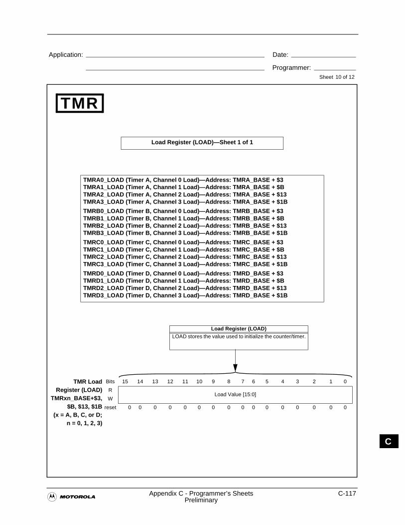
�Appendix C - Programmer’s Sheets C-117
Preliminary
Application: Date:
Programmer:Sheet
C
TMR
10 of 12
TMRA0_LOAD (Timer A, Channel 0 Load)—Address: TMRA_BASE + $3TMRA1_LOAD (Timer A, Channel 1 Load)—Address: TMRA_BASE + $BTMRA2_LOAD (Timer A, Channel 2 Load)—Address: TMRA_BASE + $13TMRA3_LOAD (Timer A, Channel 3 Load)—Address: TMRA_BASE + $1B
TMRB0_LOAD (Timer B, Channel 0 Load)—Address: TMRB_BASE + $3TMRB1_LOAD (Timer B, Channel 1 Load)—Address: TMRB_BASE + $BTMRB2_LOAD (Timer B, Channel 2 Load)—Address: TMRB_BASE + $13TMRB3_LOAD (Timer B, Channel 3 Load)—Address: TMRB_BASE + $1B
TMRC0_LOAD (Timer C, Channel 0 Load)—Address: TMRC_BASE + $3TMRC1_LOAD (Timer C, Channel 1 Load)—Address: TMRC_BASE + $BTMRC2_LOAD (Timer C, Channel 2 Load)—Address: TMRC_BASE + $13TMRC3_LOAD (Timer C, Channel 3 Load)—Address: TMRC_BASE + $1B
TMRD0_LOAD (Timer D, Channel 0 Load)—Address: TMRD_BASE + $3TMRD1_LOAD (Timer D, Channel 1 Load)—Address: TMRD_BASE + $BTMRD2_LOAD (Timer D, Channel 2 Load)—Address: TMRD_BASE + $13TMRD3_LOAD (Timer D, Channel 3 Load)—Address: TMRD_BASE + $1B
Load Register (LOAD)LOAD stores the value used to initialize the counter/timer.
TMR LoadRegister (LOAD)
TMRxn_BASE+$3,$B, $13, $1B
(x = A, B, C, or D;n = 0, 1, 2, 3)
Bits 15 14 13 12 11 10 9 8 7 6 5 4 3 2 1 0
RLoad Value [15:0]
W
reset 0 0 0 0 0 0 0 0 0 0 0 0 0 0 0 0
Load Register (LOAD)—Sheet 1 of 1
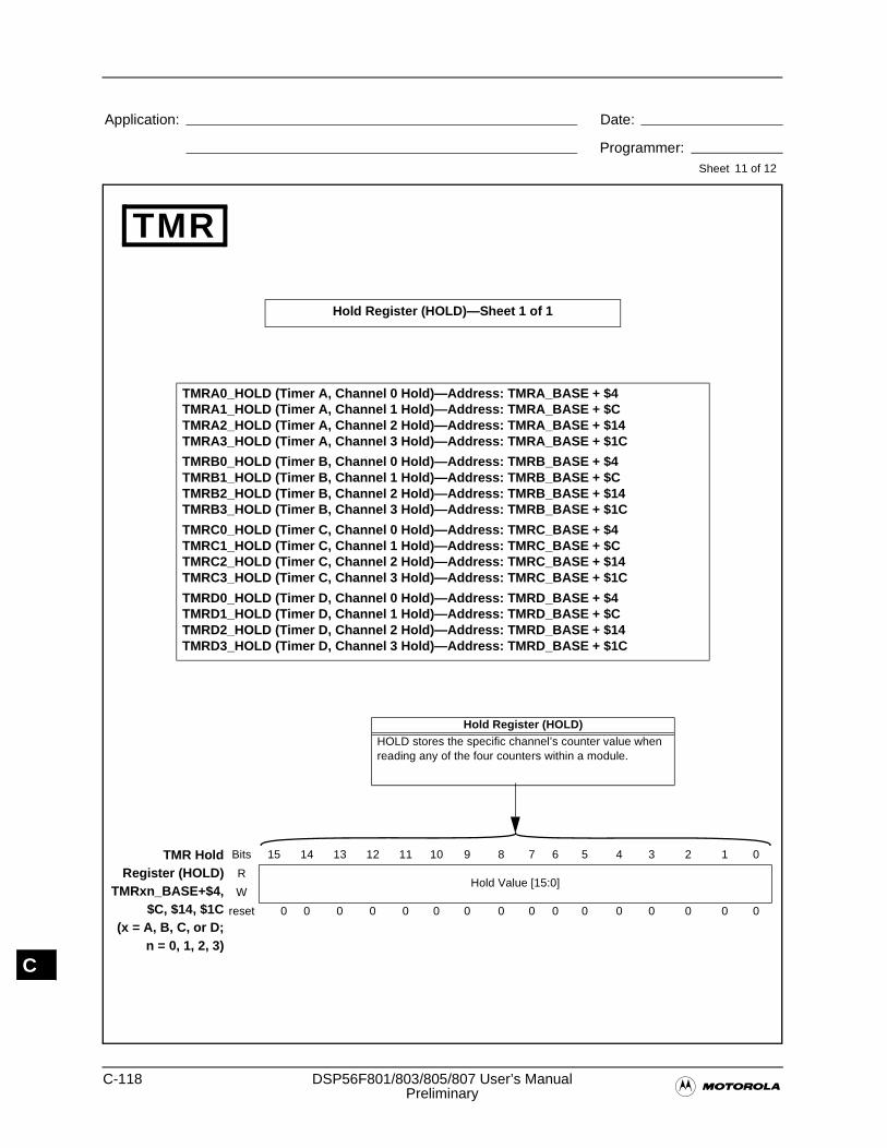
C-118 DSP56F801/803/805/807 User’s Manual�Preliminary
Application: Date:
Programmer:Sheet
C
TMR
11 of 12
TMRA0_HOLD (Timer A, Channel 0 Hold)—Address: TMRA_BASE + $4TMRA1_HOLD (Timer A, Channel 1 Hold)—Address: TMRA_BASE + $CTMRA2_HOLD (Timer A, Channel 2 Hold)—Address: TMRA_BASE + $14TMRA3_HOLD (Timer A, Channel 3 Hold)—Address: TMRA_BASE + $1C
TMRB0_HOLD (Timer B, Channel 0 Hold)—Address: TMRB_BASE + $4TMRB1_HOLD (Timer B, Channel 1 Hold)—Address: TMRB_BASE + $CTMRB2_HOLD (Timer B, Channel 2 Hold)—Address: TMRB_BASE + $14TMRB3_HOLD (Timer B, Channel 3 Hold)—Address: TMRB_BASE + $1C
TMRC0_HOLD (Timer C, Channel 0 Hold)—Address: TMRC_BASE + $4TMRC1_HOLD (Timer C, Channel 1 Hold)—Address: TMRC_BASE + $CTMRC2_HOLD (Timer C, Channel 2 Hold)—Address: TMRC_BASE + $14TMRC3_HOLD (Timer C, Channel 3 Hold)—Address: TMRC_BASE + $1C
TMRD0_HOLD (Timer D, Channel 0 Hold)—Address: TMRD_BASE + $4TMRD1_HOLD (Timer D, Channel 1 Hold)—Address: TMRD_BASE + $CTMRD2_HOLD (Timer D, Channel 2 Hold)—Address: TMRD_BASE + $14TMRD3_HOLD (Timer D, Channel 3 Hold)—Address: TMRD_BASE + $1C
Hold Register (HOLD)HOLD stores the specific channel’s counter value when reading any of the four counters within a module.
TMR HoldRegister (HOLD)
TMRxn_BASE+$4,$C, $14, $1C
(x = A, B, C, or D;n = 0, 1, 2, 3)
Bits 15 14 13 12 11 10 9 8 7 6 5 4 3 2 1 0
RHold Value [15:0]
W
reset 0 0 0 0 0 0 0 0 0 0 0 0 0 0 0 0
Hold Register (HOLD)—Sheet 1 of 1
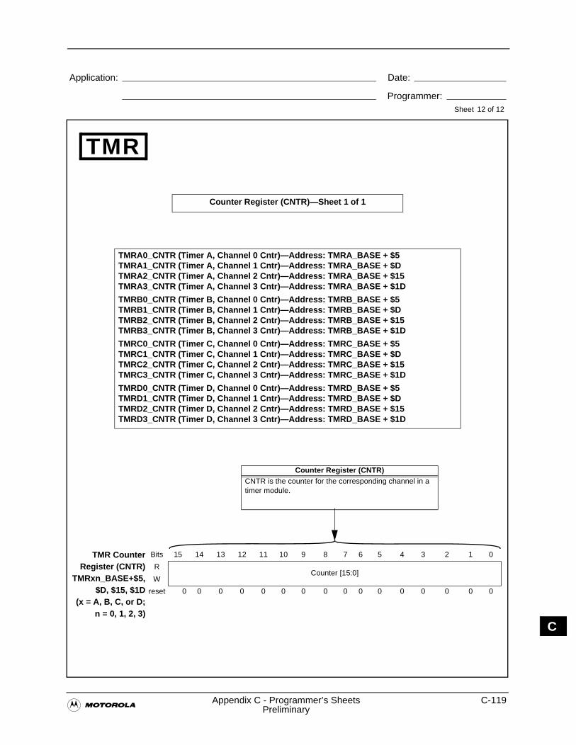
�Appendix C - Programmer’s Sheets C-119
Preliminary
Application: Date:
Programmer:Sheet
C
TMR
12 of 12
TMRA0_CNTR (Timer A, Channel 0 Cntr)—Address: TMRA_BASE + $5TMRA1_CNTR (Timer A, Channel 1 Cntr)—Address: TMRA_BASE + $DTMRA2_CNTR (Timer A, Channel 2 Cntr)—Address: TMRA_BASE + $15TMRA3_CNTR (Timer A, Channel 3 Cntr)—Address: TMRA_BASE + $1D
TMRB0_CNTR (Timer B, Channel 0 Cntr)—Address: TMRB_BASE + $5TMRB1_CNTR (Timer B, Channel 1 Cntr)—Address: TMRB_BASE + $DTMRB2_CNTR (Timer B, Channel 2 Cntr)—Address: TMRB_BASE + $15TMRB3_CNTR (Timer B, Channel 3 Cntr)—Address: TMRB_BASE + $1D
TMRC0_CNTR (Timer C, Channel 0 Cntr)—Address: TMRC_BASE + $5TMRC1_CNTR (Timer C, Channel 1 Cntr)—Address: TMRC_BASE + $DTMRC2_CNTR (Timer C, Channel 2 Cntr)—Address: TMRC_BASE + $15TMRC3_CNTR (Timer C, Channel 3 Cntr)—Address: TMRC_BASE + $1D
TMRD0_CNTR (Timer D, Channel 0 Cntr)—Address: TMRD_BASE + $5TMRD1_CNTR (Timer D, Channel 1 Cntr)—Address: TMRD_BASE + $DTMRD2_CNTR (Timer D, Channel 2 Cntr)—Address: TMRD_BASE + $15TMRD3_CNTR (Timer D, Channel 3 Cntr)—Address: TMRD_BASE + $1D
Counter Register (CNTR)CNTR is the counter for the corresponding channel in a timer module.
TMR CounterRegister (CNTR)
TMRxn_BASE+$5,$D, $15, $1D
(x = A, B, C, or D;n = 0, 1, 2, 3)
Bits 15 14 13 12 11 10 9 8 7 6 5 4 3 2 1 0
RCounter [15:0]
W
reset 0 0 0 0 0 0 0 0 0 0 0 0 0 0 0 0
Counter Register (CNTR)—Sheet 1 of 1
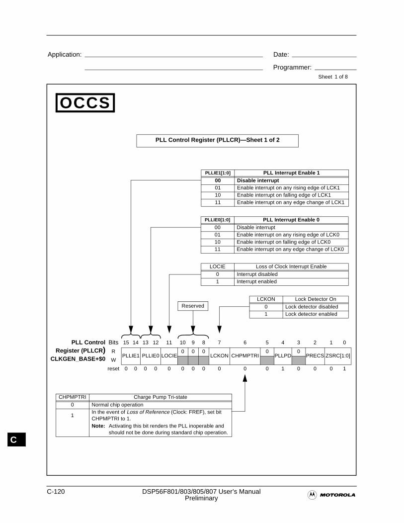
C-120 DSP56F801/803/805/807 User’s Manual�Preliminary
Application: Date:
Programmer:Sheet
C
OCCS
1 of 8
PLL ControlRegister (PLLCR)
CLKGEN_BASE+$0
Bits 15 14 13 12 11 10 9 8 7 6 5 4 3 2 1 0
RPLLIE1 PLLIE0 LOCIE
0 0 0LCKON CHPMPTRI
0PLLPD
0PRECS ZSRC[1:0]
W
reset 0 0 0 0 0 0 0 0 0 0 0 1 0 0 0 1
PLLIE1[1:0] PLL Interrupt Enable 100 Disable interrupt01 Enable interrupt on any rising edge of LCK110 Enable interrupt on falling edge of LCK111 Enable interrupt on any edge change of LCK1
PLLIE0[1:0] PLL Interrupt Enable 000 Disable interrupt01 Enable interrupt on any rising edge of LCK010 Enable interrupt on falling edge of LCK011 Enable interrupt on any edge change of LCK0
LOCIE Loss of Clock Interrupt Enable
0 Interrupt disabled1 Interrupt enabled
LCKON Lock Detector On
0 Lock detector disabled1 Lock detector enabled
CHPMPTRI Charge Pump Tri-state
0 Normal chip operation
1In the event of Loss of Reference (Clock: FREF), set bit CHPMPTRI to 1. Note: Activating this bit renders the PLL inoperable and
should not be done during standard chip operation.
Reserved
PLL Control Register (PLLCR)—Sheet 1 of 2
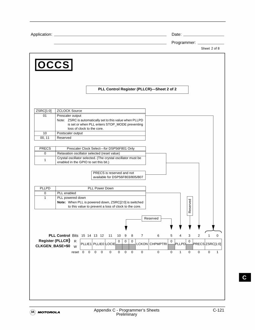
�Appendix C - Programmer’s Sheets C-121
Preliminary
Application: Date:
Programmer:Sheet
C
OCCS
2 of 8
PLL ControlRegister (PLLCR)
CLKGEN_BASE+$0
Bits 15 14 13 12 11 10 9 8 7 6 5 4 3 2 1 0
RPLLIE1 PLLIE0 LOCIE
0 0 0LCKON CHPMPTRI
0PLLPD
0PRECS ZSRC[1:0]
W
reset 0 0 0 0 0 0 0 0 0 0 0 1 0 0 0 1
PLLPD PLL Power Down
0 PLL enabled1 PLL powered down
Note: When PLL is powered down, ZSRC[2:0] is switched to this value to prevent a loss of clock to the core.
ZSRC[1:0] ZCLOCK Source
01 Prescaler outputNote: ZSRC is automatically set to this value when PLLPD
is set or when PLL enters STOP_MODE preventing loss of clock to the core.
10 Postscaler output00, 11 Reserved
Res
erve
d
PRECS Prescaler Clock Select—for DSP56F801 Only
0 Relaxation oscillator selected (reset value)
1Crystal oscillator selected. (The crystal oscillator must be enabled in the GPIO to set this bit.)
PRECS is reserved and not available for DSP56F803/805/807
PLL Control Register (PLLCR)—Sheet 2 of 2
Reserved
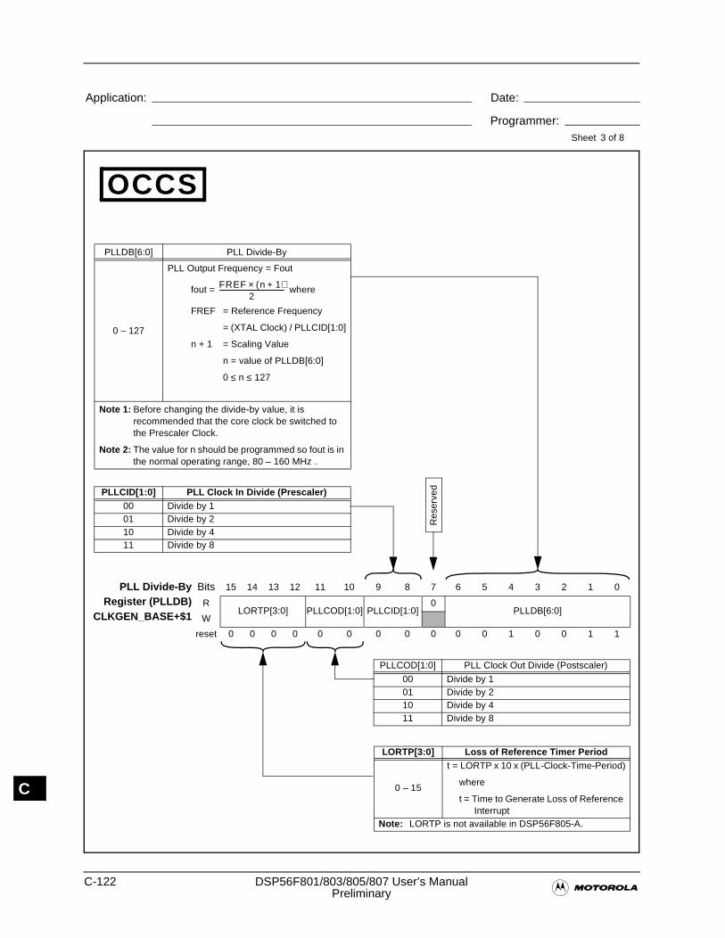
C-122 DSP56F801/803/805/807 User’s Manual�Preliminary
Application: Date:
Programmer:Sheet
C
OCCS
3 of 8
PLL Divide-ByRegister (PLLDB)
CLKGEN_BASE+$1
Bits 15 14 13 12 11 10 9 8 7 6 5 4 3 2 1 0
RLORTP[3:0] PLLCOD[1:0] PLLCID[1:0]
0PLLDB[6:0]
W
reset 0 0 0 0 0 0 0 0 0 0 0 1 0 0 1 1
PLLCID[1:0] PLL Clock In Divide (Prescaler)00 Divide by 101 Divide by 210 Divide by 411 Divide by 8
PLLCOD[1:0] PLL Clock Out Divide (Postscaler)
00 Divide by 101 Divide by 210 Divide by 411 Divide by 8
PLLDB[6:0] PLL Divide-By
0 – 127
PLL Output Frequency = Fout
fout = where
FREF = Reference Frequency
= (XTAL Clock) / PLLCID[1:0]
n + 1 = Scaling Value
n = value of PLLDB[6:0]
0 ≤ n ≤ 127
Note 1: Before changing the divide-by value, it is recommended that the core clock be switched to the Prescaler Clock.
Note 2: The value for n should be programmed so fout is in the normal operating range, 80 – 160 MHz .
FREF n 1+( )×2
-----------------------------------------
Res
erve
d
LORTP[3:0] Loss of Reference Timer Period
0 – 15
t = LORTP x 10 x (PLL-Clock-Time-Period)
where
t = Time to Generate Loss of Reference Interrupt
Note: LORTP is not available in DSP56F805-A.
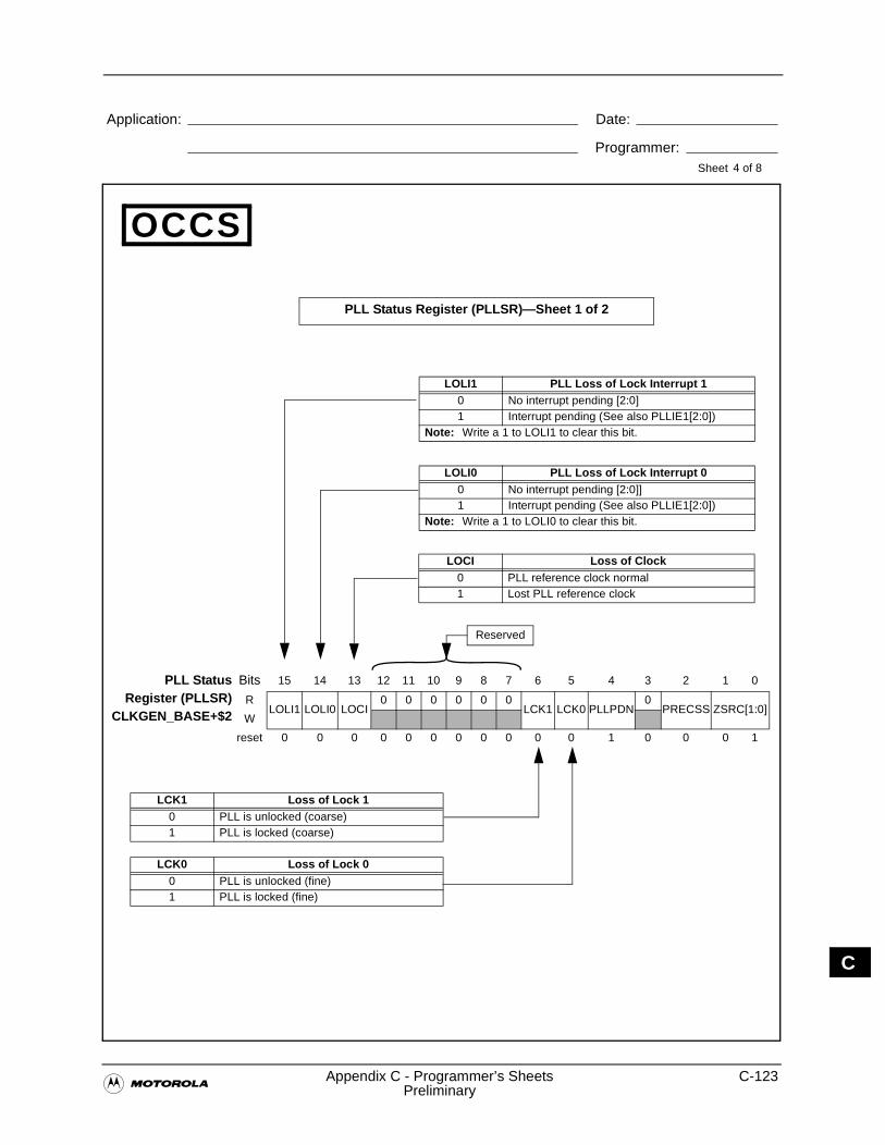
�Appendix C - Programmer’s Sheets C-123
Preliminary
Application: Date:
Programmer:Sheet
C
OCCS
4 of 8
PLL StatusRegister (PLLSR)
CLKGEN_BASE+$2
Bits 15 14 13 12 11 10 9 8 7 6 5 4 3 2 1 0
RLOLI1 LOLI0 LOCI
0 0 0 0 0 0LCK1 LCK0 PLLPDN
0PRECSS ZSRC[1:0]
W
reset 0 0 0 0 0 0 0 0 0 0 0 1 0 0 0 1
LOLI0 PLL Loss of Lock Interrupt 00 No interrupt pending [2:0]]1 Interrupt pending (See also PLLIE1[2:0])
Note: Write a 1 to LOLI0 to clear this bit.
LOLI1 PLL Loss of Lock Interrupt 10 No interrupt pending [2:0]1 Interrupt pending (See also PLLIE1[2:0])
Note: Write a 1 to LOLI1 to clear this bit.
LOCI Loss of Clock0 PLL reference clock normal1 Lost PLL reference clock
Reserved
PLL Status Register (PLLSR)—Sheet 1 of 2
LCK1 Loss of Lock 10 PLL is unlocked (coarse)1 PLL is locked (coarse)
LCK0 Loss of Lock 00 PLL is unlocked (fine)1 PLL is locked (fine)
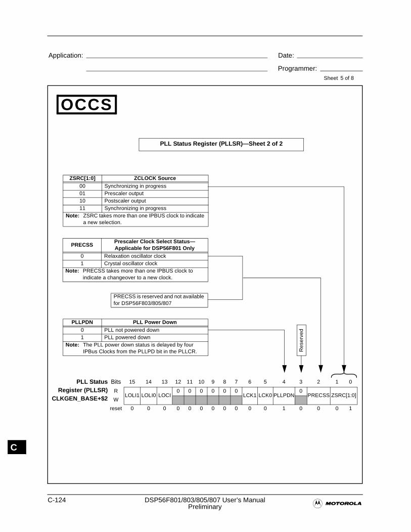
C-124 DSP56F801/803/805/807 User’s Manual�Preliminary
Application: Date:
Programmer:Sheet
C
OCCS
5 of 8
PLL StatusRegister (PLLSR)
CLKGEN_BASE+$2
Bits 15 14 13 12 11 10 9 8 7 6 5 4 3 2 1 0
RLOLI1 LOLI0 LOCI
0 0 0 0 0 0LCK1 LCK0 PLLPDN
0PRECSS ZSRC[1:0]
W
reset 0 0 0 0 0 0 0 0 0 0 0 1 0 0 0 1
PLLPDN PLL Power Down0 PLL not powered down1 PLL powered down
Note: The PLL power down status is delayed by four IPBus Clocks from the PLLPD bit in the PLLCR.
ZSRC[1:0] ZCLOCK Source00 Synchronizing in progress01 Prescaler output10 Postscaler output11 Synchronizing in progress
Note: ZSRC takes more than one IPBUS clock to indicate a new selection.
Res
erve
d
PLL Status Register (PLLSR)—Sheet 2 of 2
PRECSSPrescaler Clock Select Status—Applicable for DSP56F801 Only
0 Relaxation oscillator clock1 Crystal oscillator clock
Note: PRECSS takes more than one IPBUS clock to indicate a changeover to a new clock.
PRECSS is reserved and not available for DSP56F803/805/807
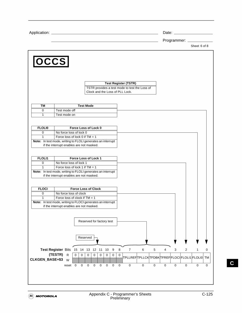
�Appendix C - Programmer’s Sheets C-125
Preliminary
Application: Date:
Programmer:Sheet
C
OCCS
6 of 8
Test Register(TESTR)
CLKGEN_BASE+$3
Bits 15 14 13 12 11 10 9 8 7 6 5 4 3 2 1 0
R 0 0 0 0 0 0 0 0TPLLREFTPLLCKTFDBKTFREF FLOCI FLOLI1 FLOLI0 TM
W
reset 0 0 0 0 0 0 0 0 0 0 0 0 0 0 0 0
Reserved for factory test
FLOLI1 Force Loss of Lock 10 No force loss of lock 11 Force loss of lock 1 if TM = 1
Note: In test mode, writing to FLOLI generates an interrupt if the interrupt enables are not masked.
FLOCI Force Loss of Clock0 No force loss of clock1 Force loss of clock if TM = 1
Note: In test mode, writing to FLOCI generates an interrupt if the interrupt enables are not masked.
FLOLI0 Force Loss of Lock 00 No force loss of lock 01 Force loss of lock 0 if TM = 1
Note: In test mode, writing to FLOLI generates an interrupt if the interrupt enables are not masked.
TM Test Mode0 Test mode off1 Test mode on
Test Register (TSTR)TSTR provides a test mode to test the Loss of Clock and the Loss of PLL Lock.
Reserved
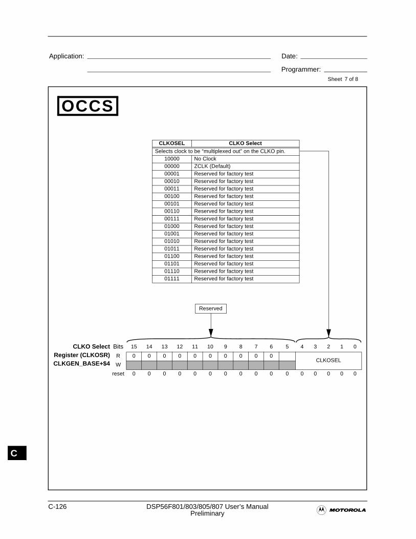
C-126 DSP56F801/803/805/807 User’s Manual�Preliminary
Application: Date:
Programmer:Sheet
C
OCCS
7 of 8
CLKO SelectRegister (CLKOSR)CLKGEN_BASE+$4
Bits 15 14 13 12 11 10 9 8 7 6 5 4 3 2 1 0
R 0 0 0 0 0 0 0 0 0 0CLKOSEL
W
reset 0 0 0 0 0 0 0 0 0 0 0 0 0 0 0 0
CLKOSEL CLKO SelectSelects clock to be “multiplexed out” on the CLKO pin.
10000 No Clock00000 ZCLK (Default)00001 Reserved for factory test00010 Reserved for factory test00011 Reserved for factory test00100 Reserved for factory test00101 Reserved for factory test00110 Reserved for factory test00111 Reserved for factory test01000 Reserved for factory test01001 Reserved for factory test01010 Reserved for factory test01011 Reserved for factory test01100 Reserved for factory test01101 Reserved for factory test01110 Reserved for factory test01111 Reserved for factory test
Reserved
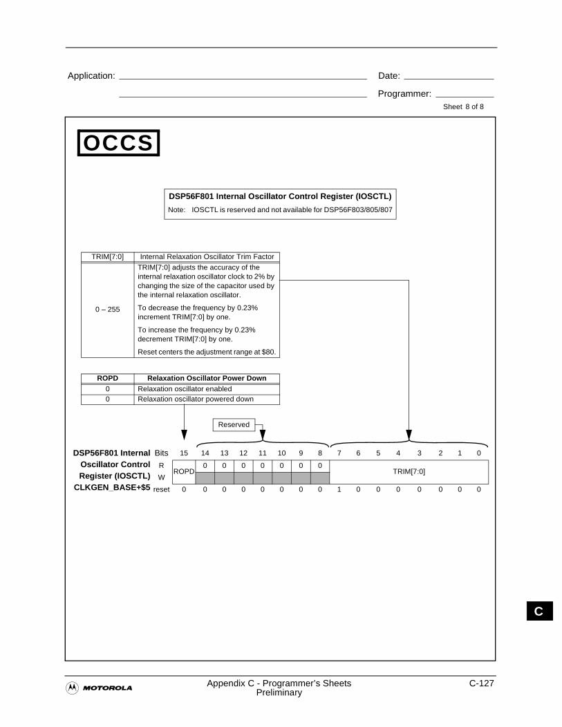
�Appendix C - Programmer’s Sheets C-127
Preliminary
Application: Date:
Programmer:Sheet
C
OCCS
8 of 8
DSP56F801 InternalOscillator ControlRegister (IOSCTL)
CLKGEN_BASE+$5
Bits 15 14 13 12 11 10 9 8 7 6 5 4 3 2 1 0
RROPD
0 0 0 0 0 0 0TRIM[7:0]
W
reset 0 0 0 0 0 0 0 0 1 0 0 0 0 0 0 0
ROPD Relaxation Oscillator Power Down0 Relaxation oscillator enabled0 Relaxation oscillator powered down
TRIM[7:0] Internal Relaxation Oscillator Trim Factor
0 – 255
TRIM[7:0] adjusts the accuracy of the internal relaxation oscillator clock to 2% by changing the size of the capacitor used by the internal relaxation oscillator.
To decrease the frequency by 0.23% increment TRIM[7:0] by one.
To increase the frequency by 0.23% decrement TRIM[7:0] by one.
Reset centers the adjustment range at $80.
Reserved
DSP56F801 Internal Oscillator Control Register (IOSCTL)
Note: IOSCTL is reserved and not available for DSP56F803/805/807
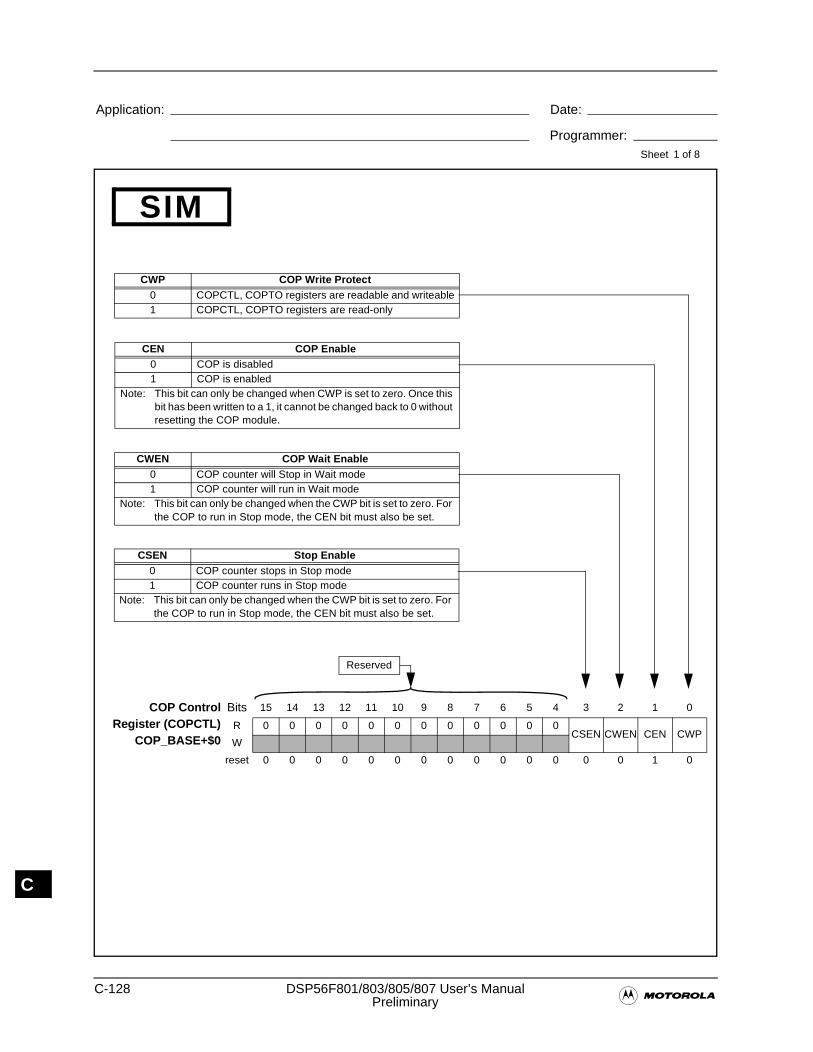
C-128 DSP56F801/803/805/807 User’s Manual�Preliminary
Application: Date:
Programmer:Sheet
C
COP ControlRegister (COPCTL)
COP_BASE+$0
Bits 15 14 13 12 11 10 9 8 7 6 5 4 3 2 1 0
R 0 0 0 0 0 0 0 0 0 0 0 0CSEN CWEN CEN CWP
W
reset 0 0 0 0 0 0 0 0 0 0 0 0 0 0 1 0
CSEN Stop Enable0 COP counter stops in Stop mode1 COP counter runs in Stop mode
Note: This bit can only be changed when the CWP bit is set to zero. For the COP to run in Stop mode, the CEN bit must also be set.
Reserved
CWEN COP Wait Enable0 COP counter will Stop in Wait mode1 COP counter will run in Wait mode
Note: This bit can only be changed when the CWP bit is set to zero. For the COP to run in Stop mode, the CEN bit must also be set.
CWP COP Write Protect0 COPCTL, COPTO registers are readable and writeable1 COPCTL, COPTO registers are read-only
CEN COP Enable0 COP is disabled1 COP is enabled
Note: This bit can only be changed when CWP is set to zero. Once this bit has been written to a 1, it cannot be changed back to 0 without resetting the COP module.
SIM
1 of 8
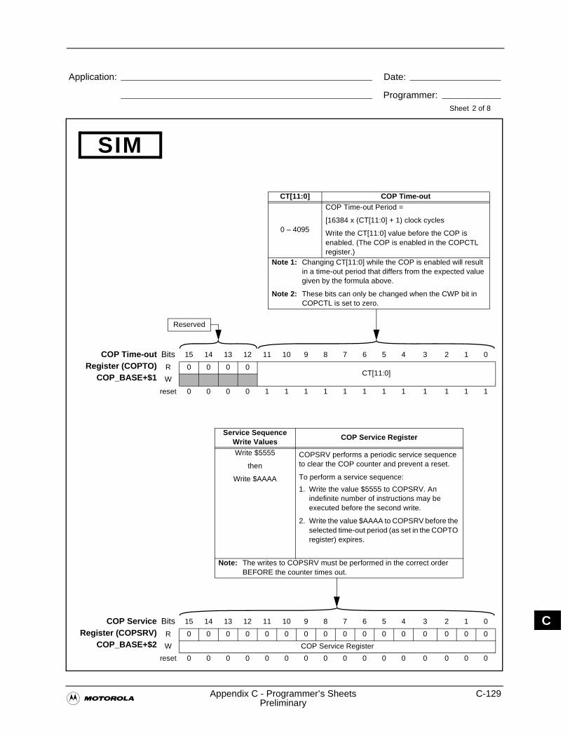
�Appendix C - Programmer’s Sheets C-129
Preliminary
Application: Date:
Programmer:Sheet
C
COP Time-outRegister (COPTO)
COP_BASE+$1
Bits 15 14 13 12 11 10 9 8 7 6 5 4 3 2 1 0
R 0 0 0 0CT[11:0]
W
reset 0 0 0 0 1 1 1 1 1 1 1 1 1 1 1 1
CT[11:0] COP Time-out
0 – 4095
COP Time-out Period =
[16384 x (CT[11:0] + 1) clock cycles
Write the CT[11:0] value before the COP is enabled. (The COP is enabled in the COPCTL register.)
Note 1: Changing CT[11:0] while the COP is enabled will result in a time-out period that differs from the expected value given by the formula above.
Note 2: These bits can only be changed when the CWP bit in COPCTL is set to zero.
Reserved
COP ServiceRegister (COPSRV)
COP_BASE+$2
Bits 15 14 13 12 11 10 9 8 7 6 5 4 3 2 1 0
R 0 0 0 0 0 0 0 0 0 0 0 0 0 0 0 0
W COP Service Register
reset 0 0 0 0 0 0 0 0 0 0 0 0 0 0 0 0
Service Sequence Write Values
COP Service Register
Write $5555
then
Write $AAAA
COPSRV performs a periodic service sequence to clear the COP counter and prevent a reset.
To perform a service sequence:
1. Write the value $5555 to COPSRV. An indefinite number of instructions may be executed before the second write.
2. Write the value $AAAA to COPSRV before the selected time-out period (as set in the COPTO register) expires.
Note: The writes to COPSRV must be performed in the correct order BEFORE the counter times out.
SIM
2 of 8
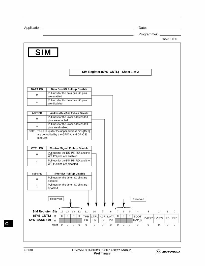
C-130 DSP56F801/803/805/807 User’s Manual�Preliminary
Application: Date:
Programmer:Sheet
C
SIM Register(SYS_CNTL)
SYS_BASE +$0
Bits 15 14 13 12 11 10 9 8 7 6 5 4 3 2 1 0
R 0 0 0 0 TMR PD
CTRL PD
ADR PD
DATA PD
0 0 0 BOOT MAP_B
LVIE27 LVIE22 PD RPDW
reset 0 0 0 0 0 0 0 0 0 0 0 0 0 0 0 0
DATA PD Data Bus I/O Pull-up Disable
0Pull-ups for the data bus I/O pins are enabled
1Pull-ups for the data bus I/O pins are disabled
Reserved
ADR PD Address Bus [5:0] Pull-up Disable
0Pull-ups for the lower address I/O pins are enabled
1Pull-ups for the lower address I/O pins are disabled
Note: The pull-ups for the upper address pins [15:6] are controlled by the GPIO A and GPIO E modules.
TMR PD Timer I/O Pull-up Disable
0Pull-ups for the timer I/O pins are enabled
1Pull-ups for the timer I/O pins are disabled
CTRL PD Control Signal Pull-up Disable
0Pull-ups for the DS, PS, RD, and the WR I/O pins are enabled
1Pull-ups for the DS, PS, RD, and the WR I/O pins are disabled
SIM Register (SYS_CNTL)—Sheet 1 of 2
Reserved
SIM
3 of 8
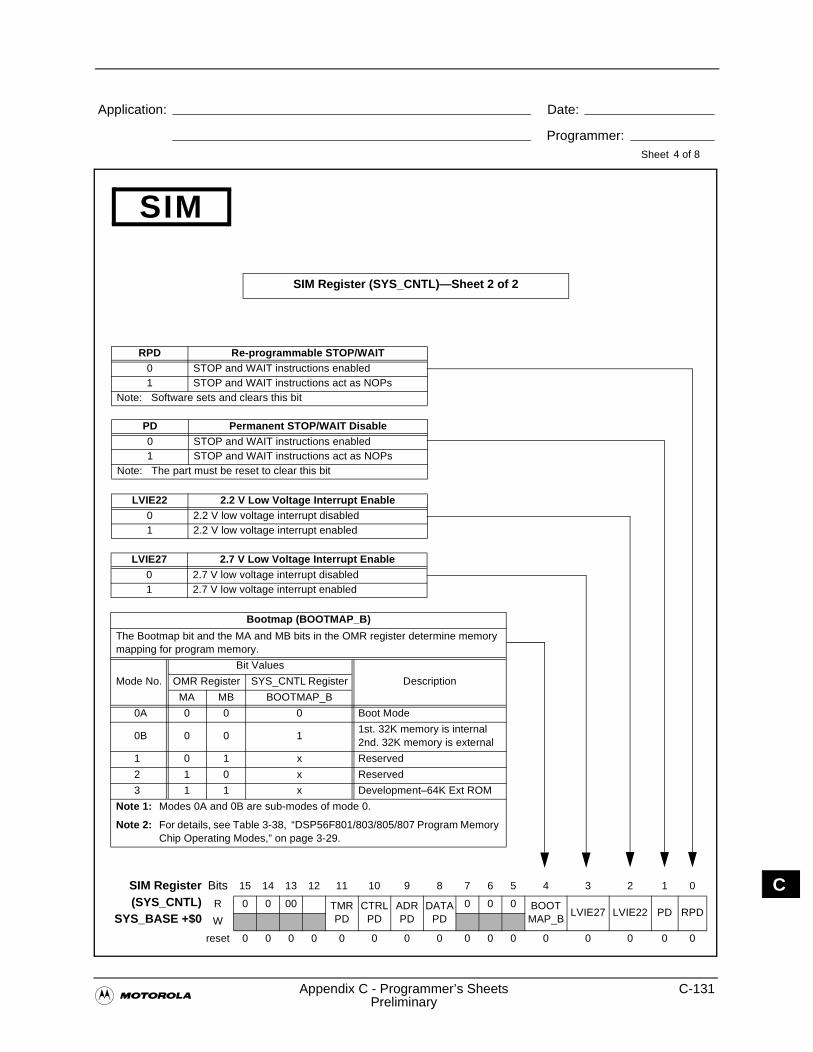
�Appendix C - Programmer’s Sheets C-131
Preliminary
Application: Date:
Programmer:Sheet
CSIM Register(SYS_CNTL)
SYS_BASE +$0
Bits 15 14 13 12 11 10 9 8 7 6 5 4 3 2 1 0
R 0 0 00 TMR PD
CTRL PD
ADR PD
DATA PD
0 0 0 BOOT MAP_B
LVIE27 LVIE22 PD RPDW
reset 0 0 0 0 0 0 0 0 0 0 0 0 0 0 0 0
LVIE27 2.7 V Low Voltage Interrupt Enable0 2.7 V low voltage interrupt disabled1 2.7 V low voltage interrupt enabled
LVIE22 2.2 V Low Voltage Interrupt Enable0 2.2 V low voltage interrupt disabled1 2.2 V low voltage interrupt enabled
RPD Re-programmable STOP/WAIT0 STOP and WAIT instructions enabled1 STOP and WAIT instructions act as NOPs
Note: Software sets and clears this bit
PD Permanent STOP/WAIT Disable0 STOP and WAIT instructions enabled1 STOP and WAIT instructions act as NOPs
Note: The part must be reset to clear this bit
Bootmap (BOOTMAP_B)
The Bootmap bit and the MA and MB bits in the OMR register determine memory mapping for program memory.
Mode No.
Bit Values
DescriptionOMR Register SYS_CNTL Register
MA MB BOOTMAP_B
0A 0 0 0 Boot Mode
0B 0 0 11st. 32K memory is internal2nd. 32K memory is external
1 0 1 x Reserved
2 1 0 x Reserved
3 1 1 x Development–64K Ext ROM
Note 1: Modes 0A and 0B are sub-modes of mode 0.
Note 2: For details, see Table 3-38, “DSP56F801/803/805/807 Program Memory Chip Operating Modes,” on page 3-29.
SIM Register (SYS_CNTL)—Sheet 2 of 2
SIM
4 of 8
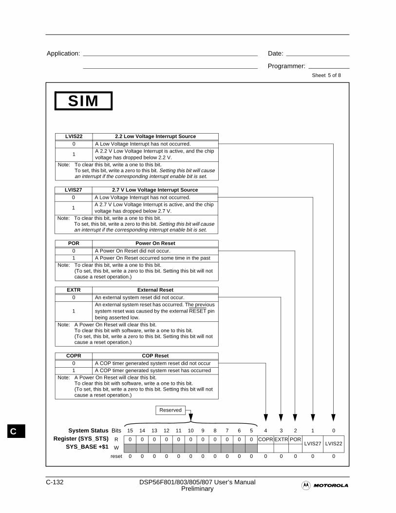
C-132 DSP56F801/803/805/807 User’s Manual�Preliminary
Application: Date:
Programmer:Sheet
C System StatusRegister (SYS_STS)
SYS_BASE +$1
Bits 15 14 13 12 11 10 9 8 7 6 5 4 3 2 1 0
R 0 0 0 0 0 0 0 0 0 0 0 COPR EXTR PORLVIS27 LVIS22
W
reset 0 0 0 0 0 0 0 0 0 0 0 0 0 0 0 0
EXTR External Reset0 An external system reset did not occur.
1An external system reset has occurred. The previous system reset was caused by the external RESET pin being asserted low.
Note: A Power On Reset will clear this bit.To clear this bit with software, write a one to this bit.(To set, this bit, write a zero to this bit. Setting this bit will not cause a reset operation.)
Reserved
POR Power On Reset0 A Power On Reset did not occur.1 A Power On Reset occurred some time in the past
Note: To clear this bit, write a one to this bit.(To set, this bit, write a zero to this bit. Setting this bit will not cause a reset operation.)
LVIS22 2.2 Low Voltage Interrupt Source0 A Low Voltage Interrupt has not occurred.
1A 2.2 V Low Voltage Interrupt is active, and the chip voltage has dropped below 2.2 V.
Note: To clear this bit, write a one to this bit.To set, this bit, write a zero to this bit. Setting this bit will cause an interrupt if the corresponding interrupt enable bit is set.
LVIS27 2.7 V Low Voltage Interrupt Source0 A Low Voltage Interrupt has not occurred.
1A 2.7 V Low Voltage Interrupt is active, and the chip voltage has dropped below 2.7 V.
Note: To clear this bit, write a one to this bit.To set, this bit, write a zero to this bit. Setting this bit will cause an interrupt if the corresponding interrupt enable bit is set.
COPR COP Reset0 A COP timer generated system reset did not occur1 A COP timer generated system reset has occurred
Note: A Power On Reset will clear this bit.To clear this bit with software, write a one to this bit.(To set, this bit, write a zero to this bit. Setting this bit will not cause a reset operation.)
SIM
5 of 8
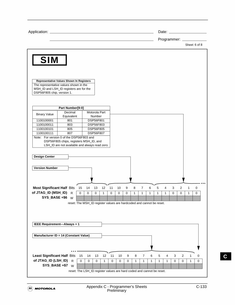
�Appendix C - Programmer’s Sheets C-133
Preliminary
Application: Date:
Programmer:Sheet
CLeast Significant Halfof JTAG_ID (LSH_ID)
SYS_BASE +$7
Bits 15 14 13 12 11 10 9 8 7 6 5 4 3 2 1 0
R 0 0 0 1 0 0 0 1 1 1 1 1 0 0 1 0
W
reset: The LSH_ID register values are hard coded and cannot be reset.
Design Center
Most Significant Halfof JTAG_ID (MSH_ID)
SYS_BASE +$6
Bits 15 14 13 12 11 10 9 8 7 6 5 4 3 2 1 0
R 0 0 0 1 0 0 0 1 1 1 1 1 0 0 1 0
W
reset: The MSH_ID register values are hardcoded and cannot be reset.
Version Number
Manufacturer ID = 14 (Constant Value)
IEEE Requirement—Always = 1
SIM
6 of 8
Part Number[9:0]
Binary ValueDecimal
EquivalentMotorola Part
Number1100100001 801 DSP56F8011100100011 803 DSP56F8031100100101 805 DSP56F8051100100111 807 DSP56F807
Note: For version 0 of the DSP56F803 and DSP56F805 chips, registers MSH_ID, and LSH_ID are not available and always read zero.
Representative Values Shown In Registers
The representative values shown in the MSH_ID and LSH_ID registers are for the DSP56F805 chip, version 1.
• • •
• • •
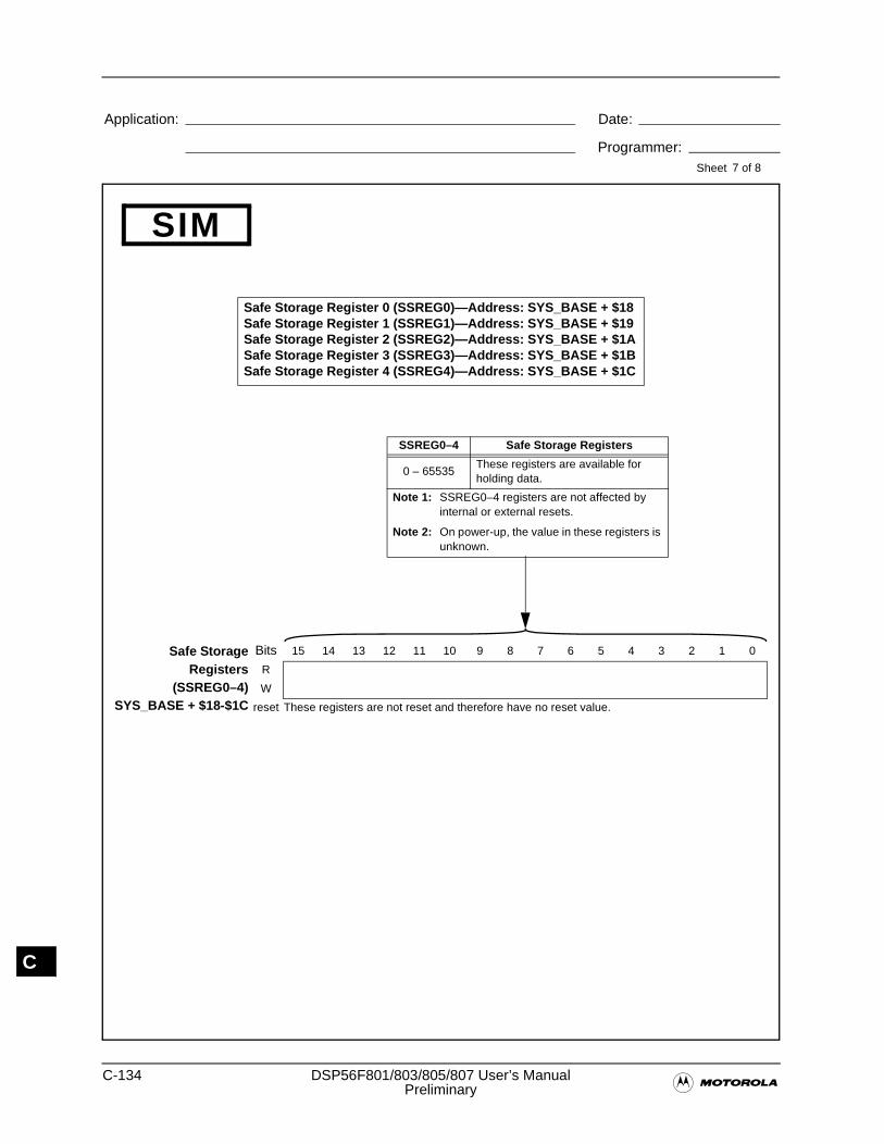
C-134 DSP56F801/803/805/807 User’s Manual�Preliminary
Application: Date:
Programmer:Sheet
C
SIM
7 of 8
Safe StorageRegisters
(SSREG0–4)SYS_BASE + $18-$1C
Bits 15 14 13 12 11 10 9 8 7 6 5 4 3 2 1 0
R
W
reset These registers are not reset and therefore have no reset value.
SSREG0–4 Safe Storage Registers
0 – 65535These registers are available for holding data.
Note 1: SSREG0–4 registers are not affected by internal or external resets.
Note 2: On power-up, the value in these registers is unknown.
Safe Storage Register 0 (SSREG0)—Address: SYS_BASE + $18Safe Storage Register 1 (SSREG1)—Address: SYS_BASE + $19Safe Storage Register 2 (SSREG2)—Address: SYS_BASE + $1ASafe Storage Register 3 (SSREG3)—Address: SYS_BASE + $1BSafe Storage Register 4 (SSREG4)—Address: SYS_BASE + $1C
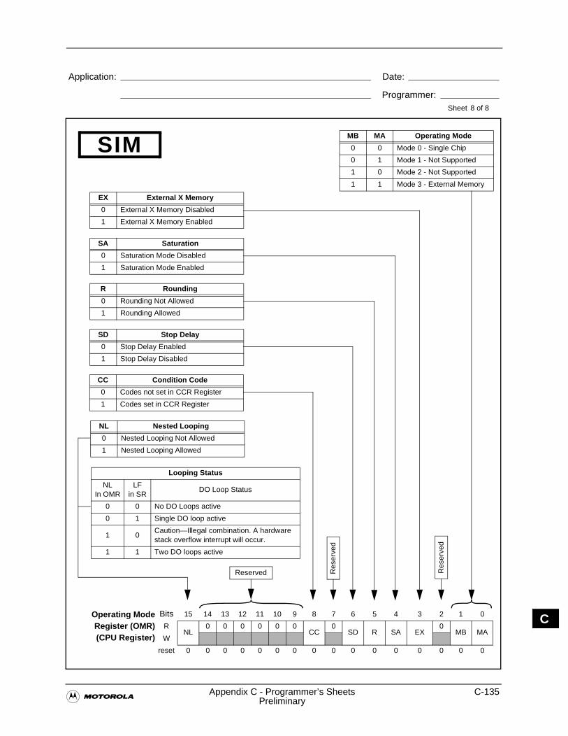
�Appendix C - Programmer’s Sheets C-135
Preliminary
Application: Date:
Programmer:Sheet
C
SIM
8 of 8
Operating ModeRegister (OMR)(CPU Register)
Bits 15 14 13 12 11 10 9 8 7 6 5 4 3 2 1 0
RNL
0 0 0 0 0 0CC
0SD R SA EX
0MB MA
W
reset 0 0 0 0 0 0 0 0 0 0 0 0 0 0 0 0
Looping Status
NL In OMR
LFin SR
DO Loop Status
0 0 No DO Loops active
0 1 Single DO loop active
1 0Caution—Illegal combination. A hardware stack overflow interrupt will occur.
1 1 Two DO loops active
CC Condition Code
0 Codes not set in CCR Register
1 Codes set in CCR Register
SD Stop Delay
0 Stop Delay Enabled
1 Stop Delay Disabled
R Rounding
0 Rounding Not Allowed
1 Rounding Allowed
SA Saturation
0 Saturation Mode Disabled
1 Saturation Mode Enabled
EX External X Memory
0 External X Memory Disabled
1 External X Memory Enabled
Reserved
MB MA Operating Mode
0 0 Mode 0 - Single Chip
0 1 Mode 1 - Not Supported
1 0 Mode 2 - Not Supported
1 1 Mode 3 - External Memory
Res
erve
d
Res
erve
d
NL Nested Looping
0 Nested Looping Not Allowed
1 Nested Looping Allowed

C-136 DSP56F801/803/805/807 User’s Manual�Preliminary
C

�Appendix E - Packaging & Pinout Information D-1
Preliminary
D N
Appendix DPackaging & Pinout Information

D-2 DSP56F801/803/805/807 User’s Manual�Preliminary
D
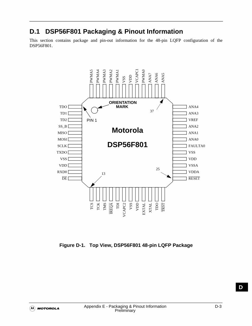
�Appendix E - Packaging & Pinout Information D-3
Preliminary
D N
D.1 DSP56F801 Packaging & Pinout InformationThis section contains package and pin-out information for the 48-pin LQFP configuration of theDSP56F801.
Figure D-1. Top View, DSP56F801 48-pin LQFP Package
PIN 1
ORIENTATIONMARKTDO
TD1
TD2
SS_B
MISO
MOSI
SCLK
TXDO
VSS
VDD
RXD0
DE
TC
S
TC
K
TM
S
IRE
QA
TD
I
VC
APC
2
VS
S
VD
D
EX
TA
L
XT
AL
TD
O
TR
ST
ANA4
ANA3
VREF
ANA2
ANA1
ANA0
FAULTA0
VSS
VDD
VSSA
VDDA
RESET
PWM
A5
PWM
A4
PWM
A3
PWM
A2
PWM
A1
VSS
VD
D
VC
APC
1
PWM
A0
AN
A7
AN
A6
AN
A5
13
37
25
Motorola
DSP56F801
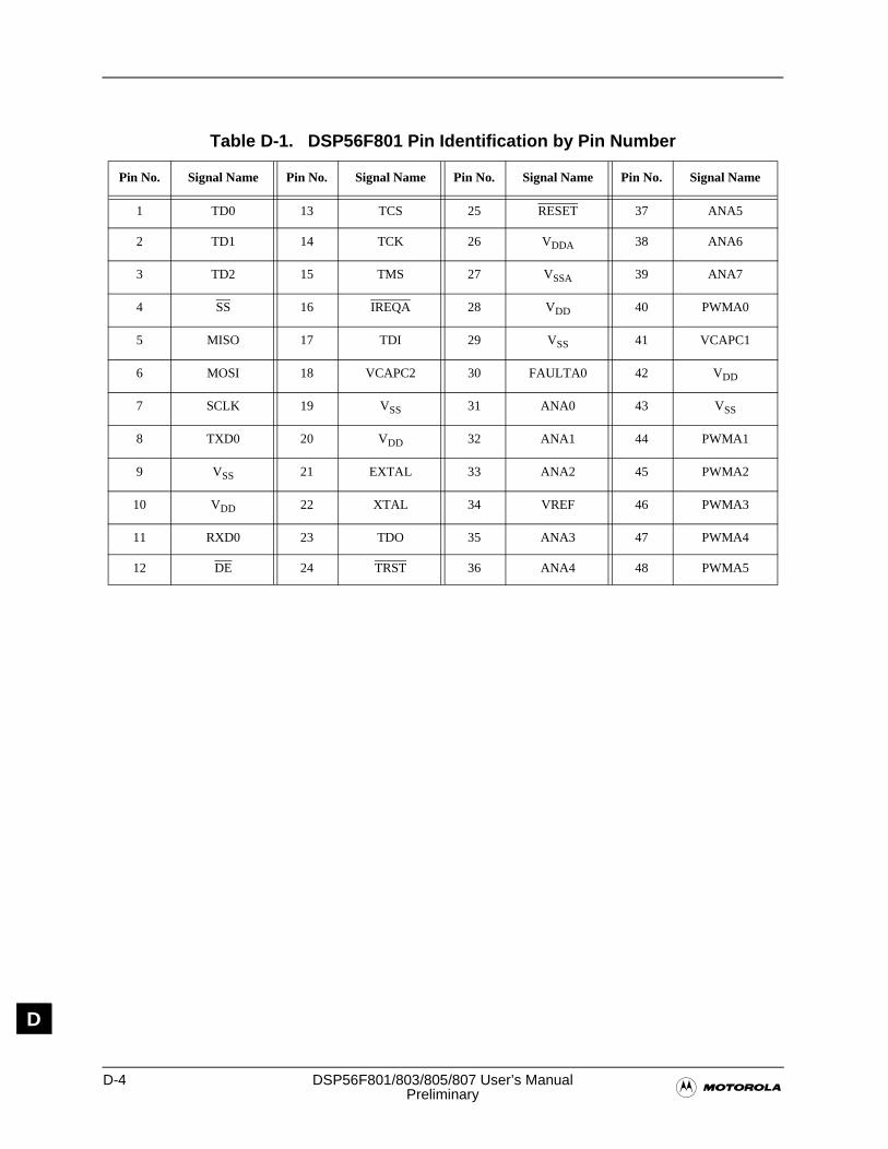
D-4 DSP56F801/803/805/807 User’s Manual�Preliminary
D
Table D-1. DSP56F801 Pin Identification by Pin Number
Pin No. Signal Name Pin No. Signal Name Pin No. Signal Name Pin No. Signal Name
1 TD0 13 TCS 25 RESET 37 ANA5
2 TD1 14 TCK 26 VDDA 38 ANA6
3 TD2 15 TMS 27 VSSA 39 ANA7
4 SS 16 IREQA 28 VDD 40 PWMA0
5 MISO 17 TDI 29 VSS 41 VCAPC1
6 MOSI 18 VCAPC2 30 FAULTA0 42 VDD
7 SCLK 19 VSS 31 ANA0 43 VSS
8 TXD0 20 VDD 32 ANA1 44 PWMA1
9 VSS 21 EXTAL 33 ANA2 45 PWMA2
10 VDD 22 XTAL 34 VREF 46 PWMA3
11 RXD0 23 TDO 35 ANA3 47 PWMA4
12 DE 24 TRST 36 ANA4 48 PWMA5
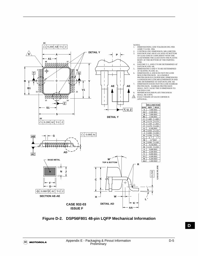
�Appendix E - Packaging & Pinout Information D-5
Preliminary
D NFigure D-2. DSP56F801 48-pin LQFP Mechanical Information
A
A1
Z0.200 AB T-U
4X
Z0.200 AC T-U
4X
B
B1
1
12
13 24
25
36
3748
S1
S
V
V1
P
AE AE
T, U, Z
DETAIL Y
DETAIL Y
BASE METAL
N J
FD
T-UM0.080 ZAC
SECTION AE-AE
AD
G 0.080 AC
M°TOP & BOTTOM
L °W
K
AA
EC
H
0.25
0
R
9
DETAIL AD
NOTES:1. DIMENSIONING AND TOLERANCING PER
ASME Y14.5M, 1994.2. CONTROLLING DIMENSION: MILLIMETER.3. DATUM PLANE AB IS LOCATED AT BOTTOM
OF LEAD AND IS COINCIDENT WITH THE LEAD WHERE THE LEAD EXITS THE PLASTIC BODY AT THE BOTTOM OF THE PARTING LINE.
4. DATUMS T, U, AND Z TO BE DETERMINED AT DATUM PLANE AB.
5. DIMENSIONS S AND V TO BE DETERMINED AT SEATING PLANE AC.
6. DIMENSIONS A AND B DO NOT INCLUDE MOLD PROTRUSION. ALLOWABLE PROTRUSION IS 0.250 PER SIDE. DIMENSIONS A AND B DO INCLUDE MOLD MISMATCH AND ARE DETERMINED AT DATUM PLANE AB.
7. DIMENSION D DOES NOT INCLUDE DAMBAR PROTRUSION. DAMBAR PROTRUSION SHALL NOT CAUSE THE D DIMENSION TO EXCEED 0.350.
8. MINIMUM SOLDER PLATE THICKNESS SHALL BE 0.0076.
9. EXACT SHAPE OF EACH CORNER IS OPTIONAL.
CASE 932-03ISSUE F
T U
Z
AB
ACG
AU
GE
PL
AN
E
DIMA
MIN MAX7.000 BSC
MILLIMETERS
A1 3.500 BSCB 7.000 BSC
B1 3.500 BSCC 1.400 1.600D 0.170 0.270E 1.350 1.450F 0.170 0.230G 0.500 BSCH 0.050 0.150J 0.090 0.200K 0.500 0.700
M 12 REFN 0.090 0.160P 0.250 BSC
L 0 7
R 0.150 0.250S 9.000 BSCS1 4.500 BSCV 9.000 BSCV1 4.500 BSCW 0.200 REFAA 1.000 REF
°° °
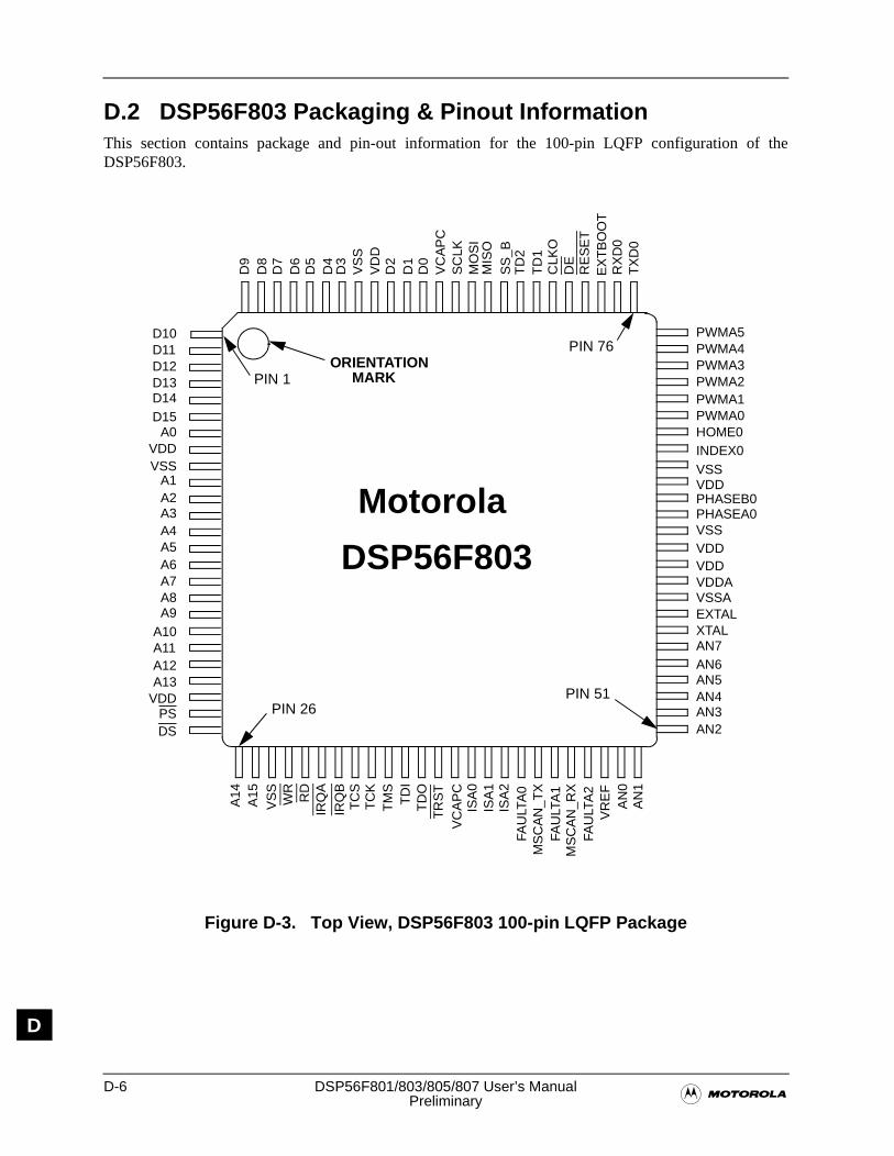
D-6 DSP56F801/803/805/807 User’s Manual�Preliminary
D
D.2 DSP56F803 Packaging & Pinout InformationThis section contains package and pin-out information for the 100-pin LQFP configuration of theDSP56F803.
Figure D-3. Top View, DSP56F803 100-pin LQFP Package
PIN 1
PIN 26PIN 51
PIN 76D10D11D12D13D14D15
A0VDDVSS
A1A2A3A4A5A6A7A8A9
A10A11A12A13
VDDPSDS
A14
A15
VS
SW
RR
DIR
QA
IRQ
BT
CS
TC
KT
MS
TD
IT
DO
TR
ST
VC
AP
CIS
A0
ISA
1IS
A2
FAU
LTA
0M
SC
AN
_TX
FAU
LTA
1M
SC
AN
_RX
FAU
LTA
2V
RE
F
AN
0A
N1
PWMA5PWMA4PWMA3PWMA2PWMA1PWMA0HOME0INDEX0VSSVDDPHASEB0PHASEA0VSSVDDVDDVDDAVSSAEXTALXTALAN7AN6AN5AN4AN3AN2
D9
D8
D7
D6
D5
D4
D3
VS
SV
DD
D2
D1
D0
VC
AP
CS
CLK
MO
SI
MIS
OS
S_B
TD
2T
D1
CLK
OD
ER
ES
ET
EX
TB
OO
TR
XD
0T
XD
0
Motorola
DSP56F803
ORIENTATION MARK
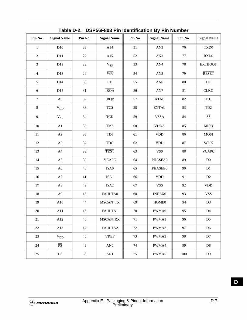
�Appendix E - Packaging & Pinout Information D-7
Preliminary
D N
Table D-2. DSP56F803 Pin Identification By Pin Number
Pin No. Signal Name Pin No. Signal Name Pin No. Signal Name Pin No. Signal Name
1 D10 26 A14 51 AN2 76 TXD0
2 D11 27 A15 52 AN3 77 RXD0
3 D12 28 VSS 53 AN4 78 EXTBOOT
4 D13 29 WR 54 AN5 79 RESET
5 D14 30 RD 55 AN6 80 DE
6 D15 31 IRQA 56 AN7 81 CLKO
7 A0 32 IRQB 57 XTAL 82 TD1
8 VDD 33 TCS 58 EXTAL 83 TD2
9 VSS 34 TCK 59 VSSA 84 SS
10 A1 35 TMS 60 VDDA 85 MISO
11 A2 36 TDI 61 VDD 86 MOSI
12 A3 37 TDO 62 VDD 87 SCLK
13 A4 38 TRST 63 VSS 88 VCAPC
14 A5 39 VCAPC 64 PHASEA0 89 D0
15 A6 40 ISA0 65 PHASEB0 90 D1
16 A7 41 ISA1 66 VDD 91 D2
17 A8 42 ISA2 67 VSS 92 VDD
18 A9 43 FAULTA0 68 INDEX0 93 VSS
19 A10 44 MSCAN_TX 69 HOME0 94 D3
20 A11 45 FAULTA1 70 PWMA0 95 D4
21 A12 46 MSCAN_RX 71 PWMA1 96 D5
22 A13 47 FAULTA2 72 PWMA2 97 D6
23 VDD 48 VREF 73 PWMA3 98 D7
24 PS 49 AN0 74 PWMA4 99 D8
25 DS 50 AN1 75 PWMA5 100 D9
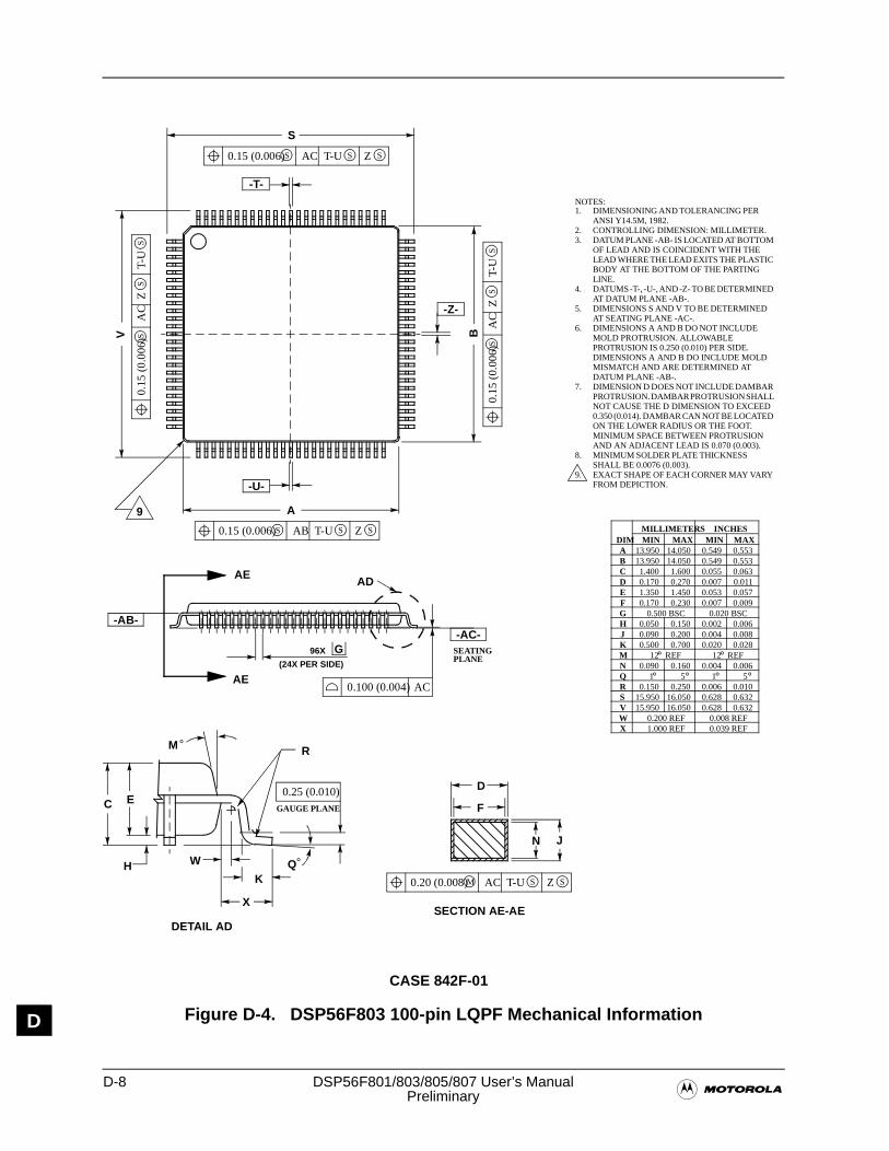
D-8 DSP56F801/803/805/807 User’s Manual�Preliminary
D Figure D-4. DSP56F803 100-pin LQPF Mechanical Information
NOTES:1. DIMENSIONING AND TOLERANCING PER
ANSI Y14.5M, 1982.2. CONTROLLING DIMENSION: MILLIMETER.3. DATUM PLANE -AB- IS LOCATED AT BOTTOM
OF LEAD AND IS COINCIDENT WITH THE LEAD WHERE THE LEAD EXITS THE PLASTIC BODY AT THE BOTTOM OF THE PARTING LINE.
4. DATUMS -T-, -U-, AND -Z- TO BE DETERMINED AT DATUM PLANE -AB-.
5. DIMENSIONS S AND V TO BE DETERMINED AT SEATING PLANE -AC-.
6. DIMENSIONS A AND B DO NOT INCLUDE MOLD PROTRUSION. ALLOWABLE PROTRUSION IS 0.250 (0.010) PER SIDE. DIMENSIONS A AND B DO INCLUDE MOLD MISMATCH AND ARE DETERMINED AT DATUM PLANE -AB-.
7. DIMENSION D DOES NOT INCLUDE DAMBAR PROTRUSION. DAMBAR PROTRUSION SHALL NOT CAUSE THE D DIMENSION TO EXCEED 0.350 (0.014). DAMBAR CAN NOT BE LOCATED ON THE LOWER RADIUS OR THE FOOT. MINIMUM SPACE BETWEEN PROTRUSION AND AN ADJACENT LEAD IS 0.070 (0.003).
8. MINIMUM SOLDER PLATE THICKNESS SHALL BE 0.0076 (0.003).
9. EXACT SHAPE OF EACH CORNER MAY VARY FROM DEPICTION.
AE
AE
AD
SEATING
(24X PER SIDE)
R
GAUGE PLANE
DETAIL ADSECTION AE-AE
SV B
A
96X
X
EC
KH W
D
F
JN
9
DIM MIN MAX MIN MAXINCHESMILLIMETERS
A 13.950 14.050 0.549 0.553B 13.950 14.050 0.549 0.553C 1.400 1.600 0.055 0.063D 0.170 0.270 0.007 0.011E 1.350 1.450 0.053 0.057F 0.170 0.230 0.007 0.009G 0.500 BSC 0.020 BSCH 0.050 0.150 0.002 0.006J 0.090 0.200 0.004 0.008K 0.500 0.700 0.020 0.028M 12 REF 12 REFN 0.090 0.160 0.004 0.006Q 1 5 1 5 R 0.150 0.250 0.006 0.010S 15.950 16.050 0.628 0.632V 15.950 16.050 0.628 0.632W 0.200 REF 0.008 REFX 1.000 REF 0.039 REF
° °
° °° °
CASE 842F-01
-T-
ST-US0.15 (0.006) Z SAC
ST-
US
0.15
(0.
006)
ZS
AC
ST-
US
0.15
(0.
006)
ZS
AC
-U-
ST-US0.15 (0.006) Z SAB
-Z-
-AC-G
PLANE
-AB-
ST-UM0.20 (0.008) Z SAC
0.100 (0.004) AC
Q°
M°
0.25 (0.010)
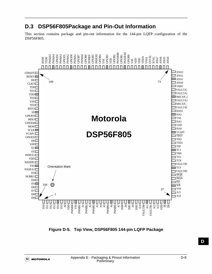
�Appendix E - Packaging & Pinout Information D-9
Preliminary
D N
D.3 DSP56F805Package and Pin-Out Information This section contains package and pin-out information for the 144-pin LQFP configuration of theDSP56F805.
Figure D-5. Top View, DSP56F805 144-pin LQFP Package
Orientation Mark
1
37
73109
D10
D11
D12
D13
D14
D15 A0
VD
DPW
MB
0V
SSPW
MB
1A
1PW
MB
2A
2PW
MB
3A
3A
4A
5PW
MB
4A
6PW
MB
5A
7IS
B0
A8
ISB
1A
9IS
B2
A10
FAU
LTB
0A
11FA
ULT
B1
A12
A13
VD
D PS DS
RX
D0
TXD
0PW
MA
5PW
MA
4G
PIO
D2
PWM
A3
GPI
OD
1PW
MA
2G
PIO
D0
PWM
A1
GPI
OB
7PW
MA
0G
PIO
B6
HO
ME0
GPI
OB
5IN
DEX
0G
PIO
B4
VSS
GPI
OB
3V
DD
GPI
OB
2PH
ASE
B0
GPI
OB
1PH
ASE
A0
GPI
OB
0V
SSV
DD
VD
DV
DD
AV
SSA
EXTA
LX
TAL
AN
A7
AN
A6
AN
A5
AN
A4
144
Motorola
DSP56F805
XTBOOTRESET
DECLKO
TD0TD1
VDDTD2VSSTD3
RSTOSS
GPIOD3MISO
GPIOD4MOSISCLK
VCAPCGPIOD5
D0VPP
D1D2
INDEX1VDD
HASEB1VSS
HASEA1D3
HOME1D4D5D6D7D8D9
ANA3ANA2ANA1ANA0VREFFAULTA3FAULTA2MSCAN_RFAULTA1MSCAN_TFAULTA0RXD1ISA2VSSISA1VDDISA0VCAPCTRSTTDOTXD1TDITC1TMSTC0TCKFAULTB3TCSFAULTB2IRQBIRQARDWRVSSA15A14
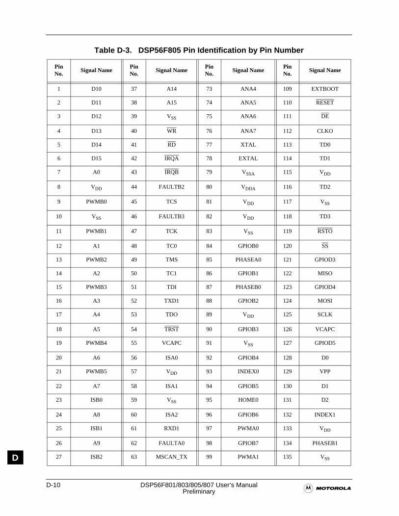
D-10 DSP56F801/803/805/807 User’s Manual�Preliminary
D
Table D-3. DSP56F805 Pin Identification by Pin Number
Pin No.
Signal NamePin No.
Signal NamePin No.
Signal NamePin No.
Signal Name
1 D10 37 A14 73 ANA4 109 EXTBOOT
2 D11 38 A15 74 ANA5 110 RESET
3 D12 39 VSS 75 ANA6 111 DE
4 D13 40 WR 76 ANA7 112 CLKO
5 D14 41 RD 77 XTAL 113 TD0
6 D15 42 IRQA 78 EXTAL 114 TD1
7 A0 43 IRQB 79 VSSA 115 VDD
8 VDD 44 FAULTB2 80 VDDA 116 TD2
9 PWMB0 45 TCS 81 VDD 117 VSS
10 VSS 46 FAULTB3 82 VDD 118 TD3
11 PWMB1 47 TCK 83 VSS 119 RSTO
12 A1 48 TC0 84 GPIOB0 120 SS
13 PWMB2 49 TMS 85 PHASEA0 121 GPIOD3
14 A2 50 TC1 86 GPIOB1 122 MISO
15 PWMB3 51 TDI 87 PHASEB0 123 GPIOD4
16 A3 52 TXD1 88 GPIOB2 124 MOSI
17 A4 53 TDO 89 VDD 125 SCLK
18 A5 54 TRST 90 GPIOB3 126 VCAPC
19 PWMB4 55 VCAPC 91 VSS 127 GPIOD5
20 A6 56 ISA0 92 GPIOB4 128 D0
21 PWMB5 57 VDD 93 INDEX0 129 VPP
22 A7 58 ISA1 94 GPIOB5 130 D1
23 ISB0 59 VSS 95 HOME0 131 D2
24 A8 60 ISA2 96 GPIOB6 132 INDEX1
25 ISB1 61 RXD1 97 PWMA0 133 VDD
26 A9 62 FAULTA0 98 GPIOB7 134 PHASEB1
27 ISB2 63 MSCAN_TX 99 PWMA1 135 VSS
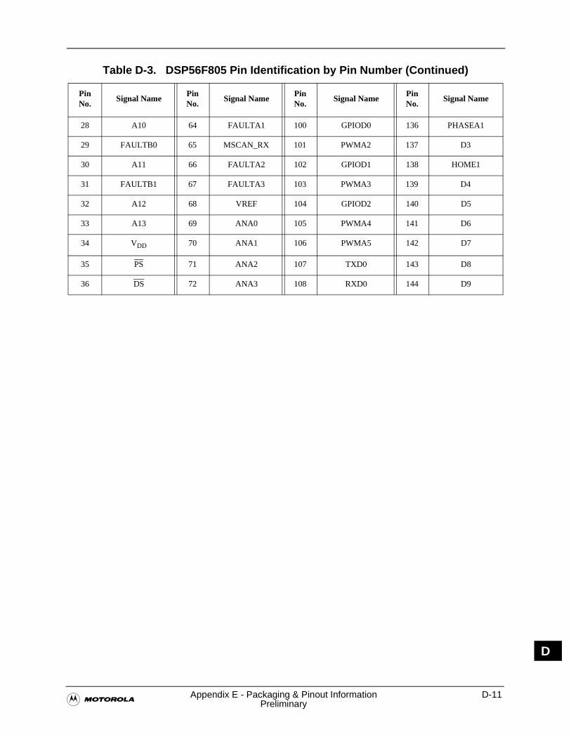
�Appendix E - Packaging & Pinout Information D-11
Preliminary
D N
28 A10 64 FAULTA1 100 GPIOD0 136 PHASEA1
29 FAULTB0 65 MSCAN_RX 101 PWMA2 137 D3
30 A11 66 FAULTA2 102 GPIOD1 138 HOME1
31 FAULTB1 67 FAULTA3 103 PWMA3 139 D4
32 A12 68 VREF 104 GPIOD2 140 D5
33 A13 69 ANA0 105 PWMA4 141 D6
34 VDD 70 ANA1 106 PWMA5 142 D7
35 PS 71 ANA2 107 TXD0 143 D8
36 DS 72 ANA3 108 RXD0 144 D9
Table D-3. DSP56F805 Pin Identification by Pin Number (Continued)
Pin No.
Signal NamePin No.
Signal NamePin No.
Signal NamePin No.
Signal Name
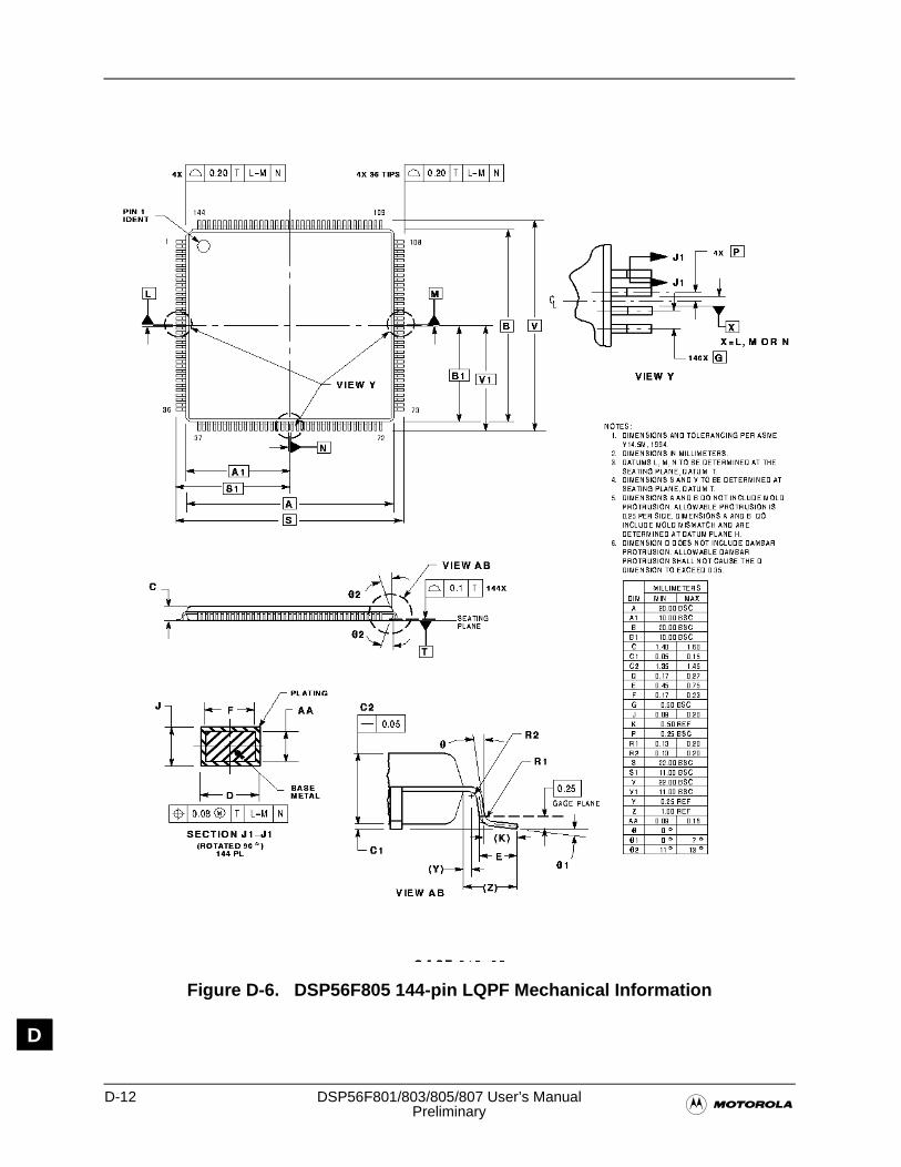
D-12 DSP56F801/803/805/807 User’s Manual�Preliminary
D
Figure D-6. DSP56F805 144-pin LQPF Mechanical Information
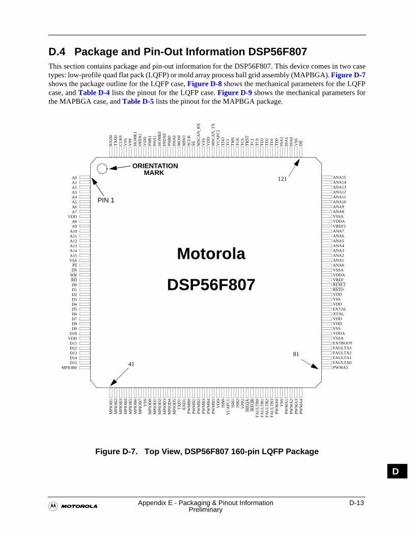
�Appendix E - Packaging & Pinout Information D-13
Preliminary
D N
D.4 Package and Pin-Out Information DSP56F807This section contains package and pin-out information for the DSP56F807. This device comes in two casetypes: low-profile quad flat pack (LQFP) or mold array process ball grid assembly (MAPBGA). Figure D-7shows the package outline for the LQFP case, Figure D-8 shows the mechanical parameters for the LQFPcase, and Table D-4 lists the pinout for the LQFP case. Figure D-9 shows the mechanical parameters forthe MAPBGA case, and Table D-5 lists the pinout for the MAPBGA package.
Figure D-7. Top View, DSP56F807 160-pin LQFP Package
A0A1A2A3A4A5A6A7
VDDA8A9
A10A11A12A13A14A15VSS
PSDS
WRRDD0D1D2D3D4D5D6D7D8D9
D10VDDD11D12D13D14D15
MPIOB0
MPI
OB
1M
PIO
B2
MPI
OB
3M
PIO
B4
MPI
OB
5M
PIO
B6
MPI
OB
7V
SSM
PIO
D0
MPI
OD
1M
PIO
D2
MPI
OD
3M
PIO
D4
MPI
OD
5T
XD
1R
XD
1P
WM
B0
PW
MB
1P
WM
B2
PW
MB
3P
WM
B4
PW
MB
5V
DD
ISB
0V
CA
PC
1IS
B1
ISB
2V
PP2
IRE
QA
IRE
QB
FA
UL
TB
0F
AU
LT
B1
FA
UL
TB
2F
AU
LT
B3
PWM
A0
VSS
PWM
A1
PWM
A2
PWM
A3
PWM
A4
PIN 1
ORIENTATIONMARK
41
121
81
ANA15ANA14ANA13ANA12ANA11ANA10ANA9ANA8VSSAVDDAVREF2ANA7ANA6ANA5ANA4ANA3ANA2ANA1ANA0VSSAVDDAVREFRESETRSTOVDDVSSVDDEXTALXTALVDDVDDVSSVDDAVSSAEXTBOOTFAULTA3FAULTA2FAULTA1FAULTA0PWMA5
RX
D0
TX
D0
CL
K0
VSS
VPP
HO
ME
1IN
DX
1V
DD
PH
B1
PH
A1
HO
ME
0IN
DX
0P
HB
0P
HA
0M
OS
IM
ISO
SC
LK
SS
MS
CA
N_R
XV
SSV
DD
MS
CA
N_T
XV
CA
PC
2T
DO
TC
IT
MS
TC
KT
CS
TR
ST
TC
1T
C0
TD
3T
D2
TD
1T
D0
ISA
2IS
A1
ISA
0V
SSD
E
Motorola
DSP56F807
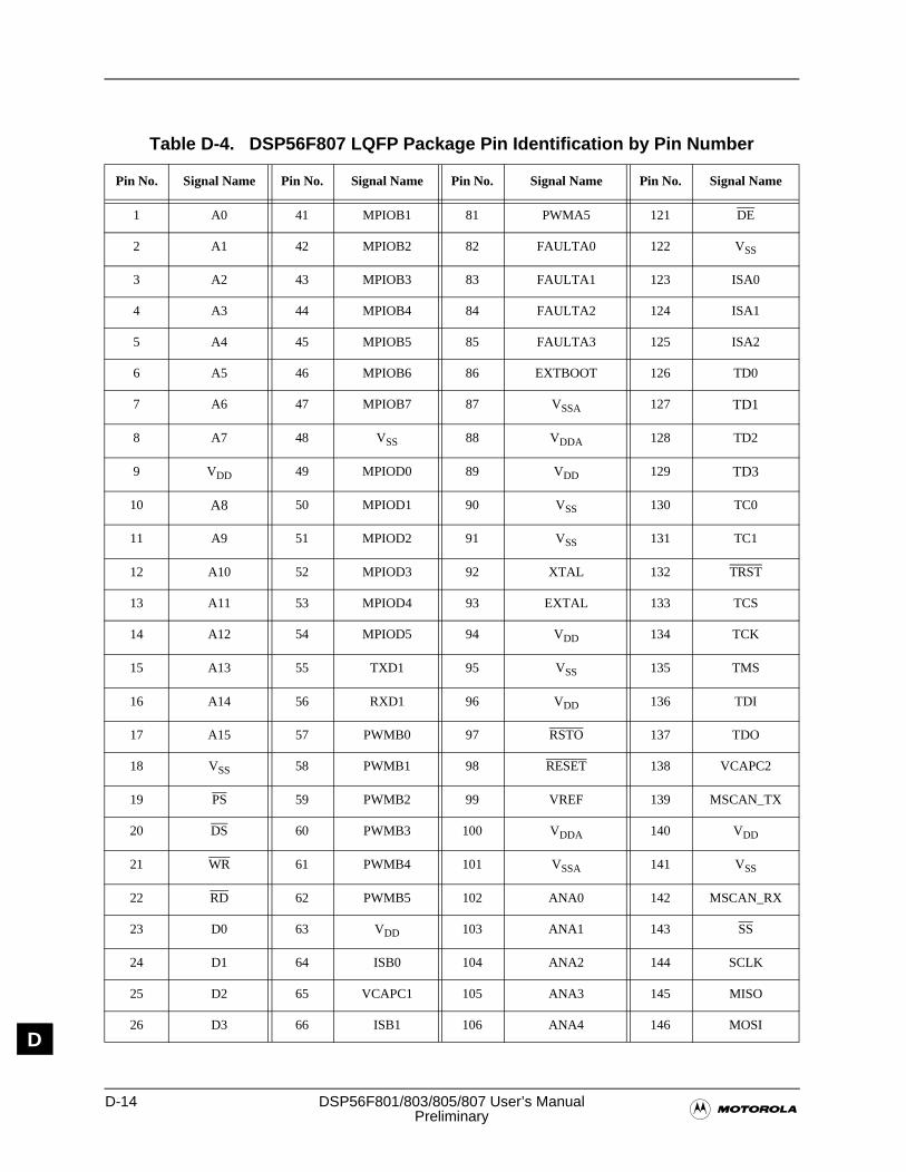
D-14 DSP56F801/803/805/807 User’s Manual�Preliminary
D
Table D-4. DSP56F807 LQFP Package Pin Identification by Pin Number
Pin No. Signal Name Pin No. Signal Name Pin No. Signal Name Pin No. Signal Name
1 A0 41 MPIOB1 81 PWMA5 121 DE
2 A1 42 MPIOB2 82 FAULTA0 122 VSS
3 A2 43 MPIOB3 83 FAULTA1 123 ISA0
4 A3 44 MPIOB4 84 FAULTA2 124 ISA1
5 A4 45 MPIOB5 85 FAULTA3 125 ISA2
6 A5 46 MPIOB6 86 EXTBOOT 126 TD0
7 A6 47 MPIOB7 87 VSSA 127 TD1
8 A7 48 VSS 88 VDDA 128 TD2
9 VDD 49 MPIOD0 89 VDD 129 TD3
10 A8 50 MPIOD1 90 VSS 130 TC0
11 A9 51 MPIOD2 91 VSS 131 TC1
12 A10 52 MPIOD3 92 XTAL 132 TRST
13 A11 53 MPIOD4 93 EXTAL 133 TCS
14 A12 54 MPIOD5 94 VDD 134 TCK
15 A13 55 TXD1 95 VSS 135 TMS
16 A14 56 RXD1 96 VDD 136 TDI
17 A15 57 PWMB0 97 RSTO 137 TDO
18 VSS 58 PWMB1 98 RESET 138 VCAPC2
19 PS 59 PWMB2 99 VREF 139 MSCAN_TX
20 DS 60 PWMB3 100 VDDA 140 VDD
21 WR 61 PWMB4 101 VSSA 141 VSS
22 RD 62 PWMB5 102 ANA0 142 MSCAN_RX
23 D0 63 VDD 103 ANA1 143 SS
24 D1 64 ISB0 104 ANA2 144 SCLK
25 D2 65 VCAPC1 105 ANA3 145 MISO
26 D3 66 ISB1 106 ANA4 146 MOSI
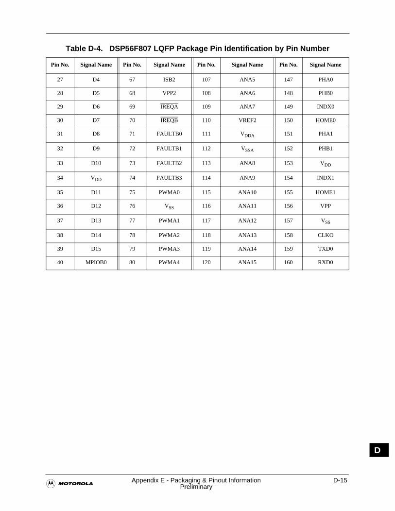
�Appendix E - Packaging & Pinout Information D-15
Preliminary
D N
27 D4 67 ISB2 107 ANA5 147 PHA0
28 D5 68 VPP2 108 ANA6 148 PHB0
29 D6 69 IREQA 109 ANA7 149 INDX0
30 D7 70 IREQB 110 VREF2 150 HOME0
31 D8 71 FAULTB0 111 VDDA 151 PHA1
32 D9 72 FAULTB1 112 VSSA 152 PHB1
33 D10 73 FAULTB2 113 ANA8 153 VDD
34 VDD 74 FAULTB3 114 ANA9 154 INDX1
35 D11 75 PWMA0 115 ANA10 155 HOME1
36 D12 76 VSS 116 ANA11 156 VPP
37 D13 77 PWMA1 117 ANA12 157 VSS
38 D14 78 PWMA2 118 ANA13 158 CLKO
39 D15 79 PWMA3 119 ANA14 159 TXD0
40 MPIOB0 80 PWMA4 120 ANA15 160 RXD0
Table D-4. DSP56F807 LQFP Package Pin Identification by Pin Number
Pin No. Signal Name Pin No. Signal Name Pin No. Signal Name Pin No. Signal Name
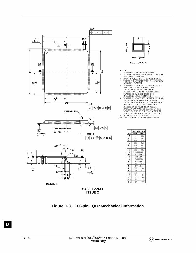
D-16 DSP56F801/803/805/807 User’s Manual�Preliminary
D
Figure D-8. 160-pin LQFP Mechanical Information
CASE 1259-01ISSUE O
DIM MIN MAXMILLIMETERS
A --- 1.60A1 0.05 0.15A2 1.35 1.45b 0.17 0.27
b1 0.17 0.23c 0.09 0.20c1 0.09 0.16D 26.00 BSC
D1 24.00 BSCe 0.50 BSCE 26.00 BSC
E1 24.00 BSCL 0.45 0.75
L1 1.00 REFR1 0.08 ---R2 0.08 0.20S 0.20 ---θ 0 7 1 0 ---2 11 13 3 11 13
0.25
6
θ
θθ ° °
° °
° °°
NOTES:1. DIMENSIONS ARE IN MILLIMETERS.2. INTERPRET DIMENSIONS AND TOLERANCES
PER ASME Y14.5M, 1994. 3. DATUMS A, B, AND D TO BE DETERMINED
WHERE THE LEADS EXIT THE PLASTIC BODY AT DATUM PLANE H.
4. DIMENSIONS D1 AND E1 DO NOT INCLUDE MOLD PROTRUSION. ALLOWABLE PROTRUSION IS 0.25mm PER SIDE. DIMENSIONS D1 AND E1 ARE MAXIMUM PLASTIC BODY SIZE DIMENSIONS INCLUDING MOLD MISMATCH.
5. DIMENSION b DOES NOT INCLUDE DAMBAR PROTRUSION. ALLOWABLE DAMBAR PROTRUSION SHALL NOT CAUSE THE LEAD WIDTH TO EXCEED THE MAXIMUM b DIMENSION BY MORE THAN 0.08mm. DAMBAR CAN NOT BE LOCATED ON THE LOWER RADIUS OR THE FOOT. MINIMUM SPACE BETWEEN A PROTRUSION AND AN ADJACENT LEAD IS 0.07mm.
6. EXACT SHAPE OF CORNERS MAY VARY.
D
BAD
GGD2
D12
E1 2
D1E
1
E 2
E
A-B0.20 DH
A-BM0.08 DC
4X
A-B0.20 DC
160X
0.08 CC
SEATINGPLANE
156X e4X e/2
160X e
DETAIL F
θ
θ2
θ1
θ3
A A2
A1
SL
(L1)
R1R2
H
GAGEPLANE
DETAIL F
c
(b)
b
c1
SECTION G-G
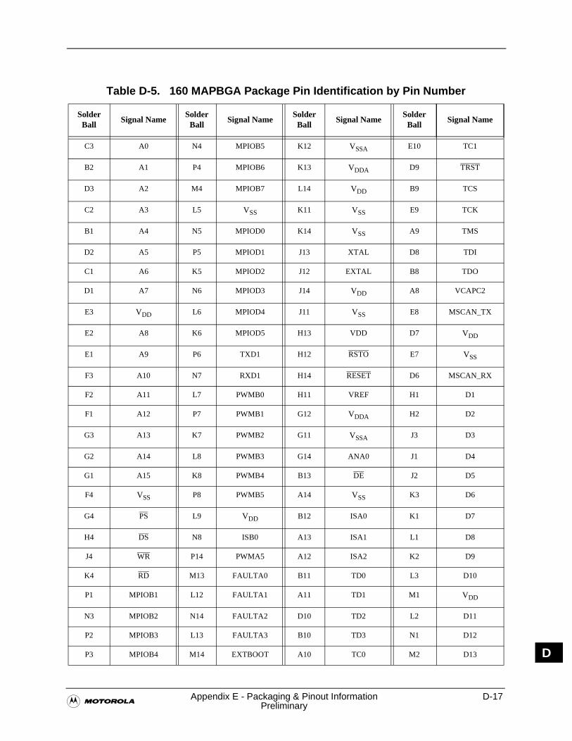
�Appendix E - Packaging & Pinout Information D-17
Preliminary
D N
Table D-5. 160 MAPBGA Package Pin Identification by Pin Number
Solder Ball
Signal NameSolder
BallSignal Name
Solder Ball
Signal NameSolder
BallSignal Name
C3 A0 N4 MPIOB5 K12 VSSA E10 TC1
B2 A1 P4 MPIOB6 K13 VDDA D9 TRST
D3 A2 M4 MPIOB7 L14 VDD B9 TCS
C2 A3 L5 VSS K11 VSS E9 TCK
B1 A4 N5 MPIOD0 K14 VSS A9 TMS
D2 A5 P5 MPIOD1 J13 XTAL D8 TDI
C1 A6 K5 MPIOD2 J12 EXTAL B8 TDO
D1 A7 N6 MPIOD3 J14 VDD A8 VCAPC2
E3 VDD L6 MPIOD4 J11 VSS E8 MSCAN_TX
E2 A8 K6 MPIOD5 H13 VDD D7 VDD
E1 A9 P6 TXD1 H12 RSTO E7 VSS
F3 A10 N7 RXD1 H14 RESET D6 MSCAN_RX
F2 A11 L7 PWMB0 H11 VREF H1 D1
F1 A12 P7 PWMB1 G12 VDDA H2 D2
G3 A13 K7 PWMB2 G11 VSSA J3 D3
G2 A14 L8 PWMB3 G14 ANA0 J1 D4
G1 A15 K8 PWMB4 B13 DE J2 D5
F4 VSS P8 PWMB5 A14 VSS K3 D6
G4 PS L9 VDD B12 ISA0 K1 D7
H4 DS N8 ISB0 A13 ISA1 L1 D8
J4 WR P14 PWMA5 A12 ISA2 K2 D9
K4 RD M13 FAULTA0 B11 TD0 L3 D10
P1 MPIOB1 L12 FAULTA1 A11 TD1 M1 VDD
N3 MPIOB2 N14 FAULTA2 D10 TD2 L2 D11
P2 MPIOB3 L13 FAULTA3 B10 TD3 N1 D12
P3 MPIOB4 M14 EXTBOOT A10 TC0 M2 D13
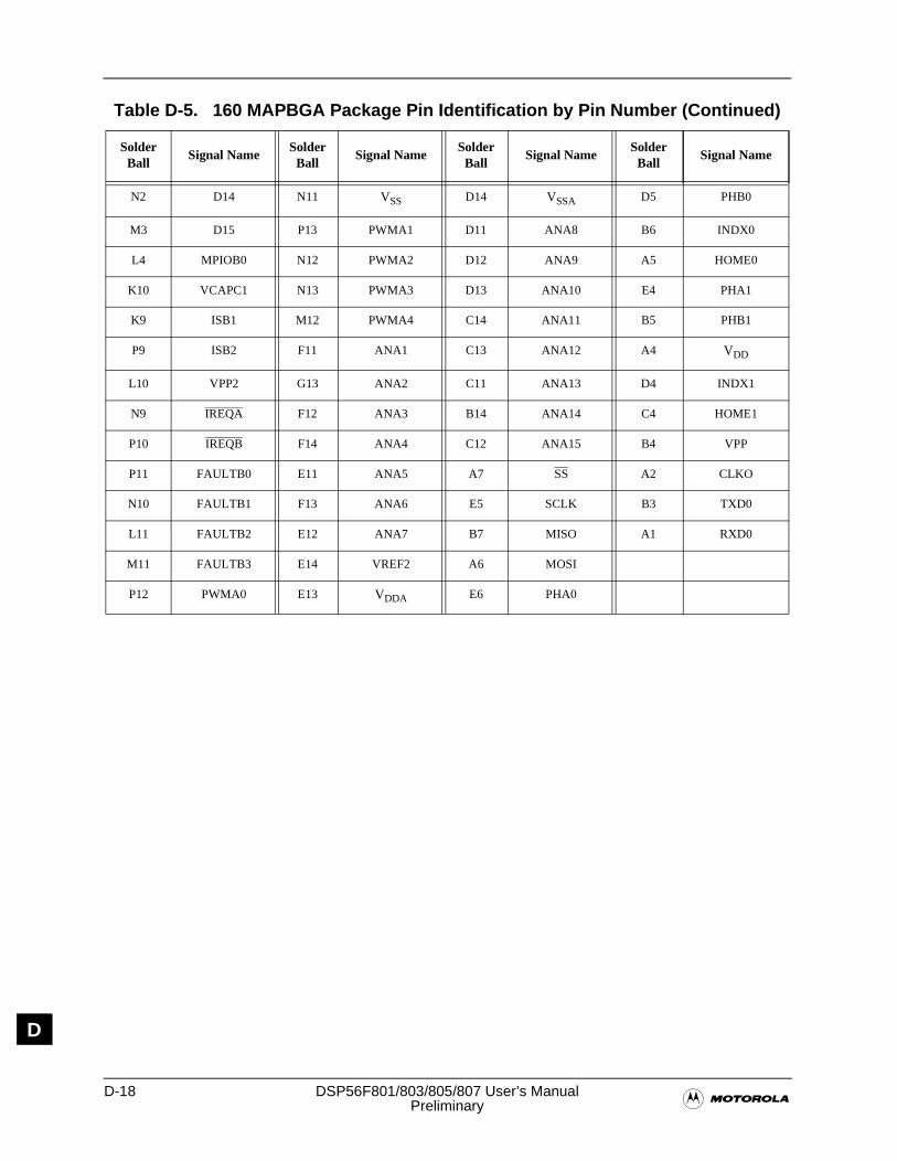
D-18 DSP56F801/803/805/807 User’s Manual�Preliminary
D
N2 D14 N11 VSS D14 VSSA D5 PHB0
M3 D15 P13 PWMA1 D11 ANA8 B6 INDX0
L4 MPIOB0 N12 PWMA2 D12 ANA9 A5 HOME0
K10 VCAPC1 N13 PWMA3 D13 ANA10 E4 PHA1
K9 ISB1 M12 PWMA4 C14 ANA11 B5 PHB1
P9 ISB2 F11 ANA1 C13 ANA12 A4 VDD
L10 VPP2 G13 ANA2 C11 ANA13 D4 INDX1
N9 IREQA F12 ANA3 B14 ANA14 C4 HOME1
P10 IREQB F14 ANA4 C12 ANA15 B4 VPP
P11 FAULTB0 E11 ANA5 A7 SS A2 CLKO
N10 FAULTB1 F13 ANA6 E5 SCLK B3 TXD0
L11 FAULTB2 E12 ANA7 B7 MISO A1 RXD0
M11 FAULTB3 E14 VREF2 A6 MOSI
P12 PWMA0 E13 VDDA E6 PHA0
Table D-5. 160 MAPBGA Package Pin Identification by Pin Number (Continued)
Solder Ball
Signal NameSolder
BallSignal Name
Solder Ball
Signal NameSolder
BallSignal Name
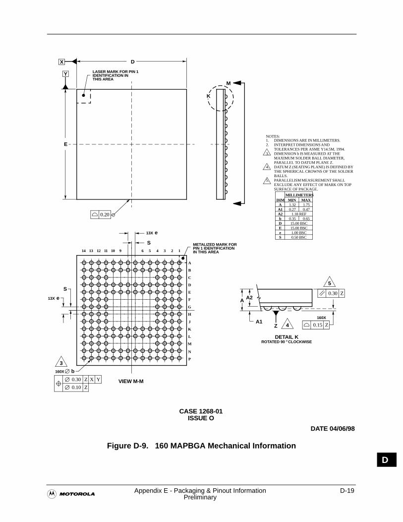
�Appendix E - Packaging & Pinout Information D-19
Preliminary
D NFigure D-9. 160 MAPBGA Mechanical Information
NOTES:1. DIMENSIONS ARE IN MILLIMETERS. 2. INTERPRET DIMENSIONS AND
TOLERANCES PER ASME Y14.5M, 1994. 3. DIMENSION b IS MEASURED AT THE
MAXIMUM SOLDER BALL DIAMETER, PARALLEL TO DATUM PLANE Z.
4. DATUM Z (SEATING PLANE) IS DEFINED BY THE SPHERICAL CROWNS OF THE SOLDER BALLS.
5. PARALLELISM MEASUREMENT SHALL EXCLUDE ANY EFFECT OF MARK ON TOP SURFACE OF PACKAGE.
CASE 1268-01ISSUE O
DATE 04/06/98
X
0.20
LASER MARK FOR PIN 1IDENTIFICATION INTHIS AREA
e13X
D
E
M
S
A1
A2A
0.15 Z
0.30 Z
Z
ROTATED 90 CLOCKWISEDETAIL K
°
5
VIEW M-M
e13X
S
X0.30 YZ
0.10 Z
3
b160X
METALIZED MARK FOR PIN 1 IDENTIFICATIONIN THIS AREA14 13 12 11 10 9 6 5 4 3 2 1
A
B
C
D
E
F
G
H
J
K
L
M
N
P
4
160X
DIM MIN MAXMILLIMETERS
A 1.32 1.75A1 0.27 0.47A2 1.18 REFb 0.35 0.65D 15.00 BSCE 15.00 BSCe 1.00 BSCS 0.50 BSC
Y
K

D-20 DSP56F801/803/805/807 User’s Manual�Preliminary
D
INDEX
DSP586801/803805807 User’s Manual Index - 1� Preliminary
A
A/D A-3ABTAK (Abort Acknowledge) bits 8-34ABTRQ (Abort Request) bits 8-35AC (Acceptance Code) bits 8-39Acceptance Code bits 8-39ACIM A-3ADC A-3
A Registers Address Map 3-23B Registers Address Map 3-24Block Diagram 9-4Channel List Registers (ADLST1 &
ADLST2) 9-16Control Register 1 (ADCR1) 9-11Control Register 2 (ADCR2) 9-15Limit Status Register (ADLSTAT) 9-20Low and High Limit Registers (ADLLMT&
ADHLMT) 9-23Offset Registers (ADOFS) 9-24Pin Descriptions 9-9Result Registers (ADRSLT) 9-22Sample Disable Register (ADSDIS) 9-17Signals 2-20Status Register (ADSTAT) 9-18Timing 9-8Zero Crossing Control Register (ADZCC) 9-15Zero Crossing Status Register (ADZCSTAT) 9-21
ADC & PWM Synchronization 1-35ADC (Analog-to-Digital Converter) 1-34ADCR A-3ADCR1 (ADC Control Register 1) 9-11ADCR2 (ADC Control Register 2) 9-15ADDLMT A-3ADDR A-3Address and Data Buses 1-22Address Bus Signals 2-12Address Generation Unit (AGU) 1-21ADHLMT A-3ADHLMT (ADC High Limit Registers) 9-23ADLLMT (ADC Low Limit Registers) 9-23ADLST A-3ADLST1 (ADC Channel List Register 2) 9-16ADLST2 (ADC Channel List Register 2) 9-16ADLSTAT A-3ADLSTAT (ADC Limit Status Register) 9-20ADM A-3ADOFS A-3ADOFS (ADC Offset Registers) 9-24ADR PD A-3
ADRSLT A-3
ADRSLT (ADC Result Registers) 9-22ADSDIS A-3ADSDIS (ADC Sample Disable Register) 9-17ADSTAT A-3ADSTAT (ADC Status Register) 9-18ADZCC A-3ADZCC (ADC Zero Crossing Control Register 9-15ADZCSTAT A-3ADZCSTAT (ADC Zero Crossing Status Register) 9-21AGU A-3AGU (Address Generation Unit) 1-21ALU A-3ALU (Data Arithmetic Logic Unit) 1-20AM (Acceptance Mask) bits 8-40Analog Input Pins 9-9Analog-to-Digital Converter (ADC) 1-34API A-3
B
Barrel Shifter A-3BCR A-3BCR (Bus Control Register) 3-6, 3-7BDC A-3BE A-3BE (Breakpoint Enable) bits 17-23BFIU A-3BFIU Registers Address Map 3-26BFLASH A-3Bit Manipulation Unit 1-21BK A-3BK (Breakpoint Configuration) bit 17-17BLDC A-3BOFFIE (Bus-Off Interrupt Enable) bit 8-33BOFFIF (Bus-Off Interrupt Flag) bit 8-31Boot Flash 3-30, 5-11Boot Flash Block Diagram 5-12BOTNEG A-3BOTNEG (Bottom-side PWM Polarity) bits 11-43Boundary Scan Register (BSR) 18-12Breakpoint and Trace Registers (OnCE) 17-26BRP (Baud Rate Prescaler) bits 8-26BS A-4BS (Breakpoint Selection) bit 17-21BSDL A-4BSR A-4BSR (Boundary Scan Register) 18-12Bus Control Register (BCR) 3-6, 3-7Bus Control Signals 2-13
BUSY bitFlash Control Register 5-17
Index - 2 DSP586801/803805807 User’s Manual�Preliminary
Flash Interface Unit Timeout Registers 5-29BYPASS instruction 18-10Bypass register 18-32
C
CAN A-4Signals 2-19
CAN Registers Address Map 3-20CAN Standard Compliant Bit Time Segment
Settings 8-21CANBTR0 (MSCAN Bus Timing Register 0) 8-25CANBTR1(MSCAN Bus Timing Register 1) 8-27CANE (Can Enable) bit 8-24CANIDAC (MSCAN Identifier Acceptance Control
Register) 8-35CANIDAR0-7 (MSCAN Identifier Acceptance
Registers) 8-38CANIDMR0-7 (MSCAN Identifier Mask
Registers) 8-39CANRFLG (MSCAN Receiver Flag Register) 8-29CANRIER (MSCAN Receiver Interrupt Enable
Register) 8-32CANRXERR (MSCAN Receive Error Counter
Register) 8-37CANTCL0 (MSCAN Control Register 0) 8-22CANTCR (MSCAN Transmitter Control Register) 8-34CANTFLG (MSCAN Transmitter Flag Register) 8-33CANTXERR (MSCAN Transmit Error Counter
Register) 8-37CAP A-4CAP (Capture Register) 14-19Capture Mode (Input Capture Mode) bit 14-16Capture Register (CAP) 14-19Capture Register Usage 14-10Cascade-count Mode 14-8CC A-4CC (Condition Code) bit 3-9CC (Condition Code) bits 16-15CEN A-4CEN (COP Enable) bit 16-8CFG A-4CGDB A-4CGDB (Core Global Data Bus) 1-22Character Length 12-11Character Transmission 12-8CHCNF A-4CHCNF (Channel Configure) bits 9-13CHPMPTRI (Charge Pump Tri-state) bit 15-10CIP (Conversion in Progress) bit 9-19CKDIVISOR A-4CLAMP instruction 18-10
CLKO A-4CLKO Select Register (CLKOSR) 15-15CLKOSEL A-4CLKOSEL (CLKO Select) bits 15-16CLKOSR A-4CLKOSR (CLKO Select Register) 15-15CLKSRC (MSCAN Clock Source) bit 8-25Clock Control 1-24Clock Generation Registers Address Map 3-27Clock Phase and Polarity Controls 13-10Clock Synthesis Module (OCCS) 1-23Clock System 8-18CMOS A-4CMP A-4CMP1 (Compare Register #1) 14-17CMP2 (Compare Register #2) 14-18CNT A-4CNTR A-4CNTR (Counter Register) 14-21Co Init (Co-channel Initialization) bit 14-13Codec A-4Compare Register #1 (CMP1) 14-17Compare Register #2 (CMP2) 14-18Compare Register Usage 14-9Computer Operating Properly (COP) Module 16-7Control Registers (CTRL) 14-11COP A-4COP (Computer Operating Properly) 16-7COP Control Register (COPCTL) 16-8COP Service Register (COPSRV) 16-9COP Time-out Register (COPTO) 16-9COP/RTI A-4COP/RTI Module 1-31COPCTL A-4COPCTL (COP Control Register) 16-8COPDIS A-4COPDIS (COP Timer disable) bit 17-16COPR A-4COPR (COP Reset) bit 16-13COPSRV A-4COPSRV (COP Service Register) 16-9COPTO A-4COPTO (COP Time-out Register 16-9Core Configuration Memory Map 3-11Core Global Data Bus (CGDB) 1-22Core Operating Modes 3-29Core Voltage Regulator 1-25Count bit 10-19Count Mode 14-6Count Mode bits 14-11Counter Register (CNTR) 14-21Counting Mode Definitions 14-6
DSP586801/803805807 User’s Manual Index - 3� Preliminary
Counting Options 14-5CPHA A-4CPHA (Clock Phase) bit 13-26CPOL A-4CPOL (Clock Polarity) bit 13-25CPU A-4CRC A-4CSEN A-5CSEN (Stop Enable) bit 16-8CSWAI (CAN Stops in Wait Mode) bit 8-22CT (COP Time-out) bits 16-9CTRL A-5CTRL (Control Register) 14-11CTRL PD A-5CWEN A-5CWEN (Cop Wait Enable) bit 16-8CWP A-5CWP (COP Write Protect) bit 16-9
D
DAC A-5DAT A-5DAT (Data Address Select) bit 17-24Data Arithmetic Logic Unit (ALU) 1-20Data Bit Recovery 12-13Data Bus 1-22Data Bus Signals 2-13Data Flash 1-27Data Flash Block Diagram 5-11Data Flash Main Block Organization 5-10Data Length Register (DLR) 8-45Data Memory Map 3-5DATA PD A-5Data RAM 1-27Data Segment Registers (DSR0-7) 8-44Data Shift Ordering 13-10Data Transmission Length 13-10DDA A-5DDR A-5DDR (Data Direction Register) 7-10DEBUG_REQUEST instruction 18-10DEC A-5DECCR (Decoder Control Register) 10-10Decoder
JTAG 18-6Decoder Control Register (DECCR) 10-10DEE A-5DEE (Dumb Erase Enable) bit 5-19Development Mode (Mode 3) 3-30DFIU A-5DFIU Registers Address Map 3-26
DFLASH A-5DIE (Watchdog Timeout Interrupt Enable) bit 10-12DIR (Count Direction) bit 14-13DIRQ A-5DIRQ (Watchdog Timeout Interrupt Request) bit 10-12DIV (Clock Divisor Select) bits 9-15DLR (Data Length Register) 8-45DPE A-5DPE (Dumb Program Enable) bit 5-18DR A-5DR (Data Register) 7-10DRV A-5DRV (Drive) bit 3-7, 6-4DS (Disable Sample) bits 9-18DSO A-5DSO (Data Shift Order) bit 13-23DSP A-5DSP 56800 Core Description 1-16DSP56F801 Peripheral Blocks 1-27DSP56F803 Peripheral Blocks 1-28DSP56F805 Peripheral Blocks 1-29DSP56F807 Peripheral Blocks 1-29DSR0-7 (Data Segment Registers) 8-44DTX (Dead Time) bits 11-38Dumb Word Programming 5-15
E
EAB (External Address Bus) 1-22EDG A-5EDG (Edge-Alighed or Center-Aligned PWMs) 11-43Edge Detect State Machine 10-6Edge-count Mode 14-7EE A-5EEOF A-5EEOF (Enable External OFLAG Force) bit 14-17EM A-5EMI (External Memory Interface) 1-30EN A-5EN (Enable) bit 17-24ENABLE_ONCE instruction 18-10ENCR A-5ENHA (Enable Hardware Acceleration) bit 11-44EOSI A-5EOSI (End of Scan Interrupt) bit 9-19EOSIE A-5EOSIE (End of Scan Interrupt Enable) bit 9-12ERASE A-5ERASE (Erase Cycle Definition) bit 5-18ERRIE A-5ERRIE (Error Interrupt Enable) bit 13-23Error Conditions 13-16
Index - 4 DSP586801/803805807 User’s Manual�Preliminary
EX A-6EX (External X Memory) bit 3-6, 3-11, 16-17Executing Programs from XRAM 3-30EXTAL 15-3EXTBOOT A-6External Address Bus (EAB) 1-22External Crystal Design Considerations 15-3External I/O Signals 13-7External Inputs 14-6External Memory Interface (EMI) 1-30external memory port
architecture 6-3External Memory Port Architecture 6-3External Reset 16-6EXTEST instruction 18-8EXTEST_PULLUP instruction 18-9EXTR A-6EXTR (External Reset) bit 16-13
F
FAULT A-6FE A-6FE (Framing Error Flag) bit 12-27Feature Matrix 1-15FFLAGx A-6FFLAGx (Faultx Pin Flag) bits 11-38FH A-6FH (FIFO Halt) bit 17-18FIEx A-6FIEx (Faultx Pin Interrupt Enable) bits 11-37Filter Interval Register (FIR) 10-13FIR A-6FIR (Filter Interval Register) 10-13FIU_ADDR (Flash Address Register) 5-20FIU_CKDIVISOR (Flash Clock Divisor Register) 5-24FIU_CNTL (Flash Control Register) 5-17FIU_DATA (Flash Data Register) 5-21FIU_EE (Flash Erase Enable Register) 5-19FIU_IE (Flash Interrupt Enable Register) 5-21FIU_IP (Flash Interrupt Pending Register) 5-23FIU_IS (Flash Interrupt Source Register) 5-22FIU_PE (Flash Program Enable Register) 5-18FIU_TERASEL (Flash Terase Limit Register) 5-24FIU_TMEL (Flash Tme Limit Register) 5-25FIU_TNVH1L (Flash TNVH1 Limit Register) 5-27FIU_TNVHL (Flash TNVH Limit Register) 5-27FIU_TNVSL (Flash Tnvs Limit Register) 5-25FIU_TPGSL (Flash Tpgs Limit Register) 5-26FIU_TPROGL (Flash Tprog Limit Register) 5-26FIU_TRCVL (Flash TRCV Limit Register) 5-28Fixed-frequency PWM Mode 14-9
FlashAddress Register (FIU_ADDR) 5-20Clock Divisor Register (FIU_CKDIVISOR) 5-24Control Register (FIU_CNTL) 5-17Data Register (FIU_DATA) 5-21Erase Enable Register (FIU_EE) 5-19Interface Unit Timeout Registers 5-28Interrupt Enable Register (FIU_IE) 5-21Interrupt Pending Register (FIU_IP) 5-23Interrupt Source Register (FIU_IS) 5-22Program Enable Register (FIU_PE) 5-18Terase Limit Register (FIU_TERASEL) 5-24Timing Relationships 5-8Tme Limit Register (FIU_TMEL) 5-25TNVH Limit Register (FIU_TNVHL) 5-27TNVH1 Limit Register (FIU_TNVH1L) 5-27Tnvs Limit Register (FIU_TNVSL) 5-25Tpgs Limit Register (FIU_TPGSL) 5-26Tprog Limit Register (FIU_TPROGL) 5-26TRCV Limit Register (FIU_TRCVL) 5-28
Flash memory A-6FLOCI A-6FLOCI (Force Loss of Clock) bit 15-15FLOLI A-6FLOLI0 (Force Loss of Lock 0) bit 15-15FLOLI1 (Force Loss of Lock) bit 15-15FMODEx A-6FMODEx (Faultx Pin Clearing Mode) bits 11-37FORCE (Force the OFLAG Output) bit 14-17FPINx A-6FPINx (Faultx Pin) bits 11-38FTACKx A-6FTACKx (Faultx Pin Acknowledge) bits 11-38
G
Gated-count Mode 14-7General Purpose I/O Port (GPIO) 1-30Glitch Filter 10-6GPIO A-6
Block Diagram 7-4Data Direction Register (DDR) 7-10Data Register (DR) 7-10Interrupt Assert Register (IAR) 7-11Interrupt Edge Sensitive Register (IESR) 7-13Interrupt Enable Register (IENR) 7-12Interrupt Pending Register (IPR) 7-12Interrupt Polarity Register (IPOLR) 7-12Interrupts 7-6Peripheral Enable Register (PER) 7-11Port A Registers Address Map 3-27Port B Registers Address Map 3-27
DSP586801/803805807 User’s Manual Index - 5� Preliminary
Port D Registers Address Map 3-28Port E Registers Address Map 3-28Programming Algorithms 7-13Programming Model 7-9Pull-Up Enable Register (PUR) 7-10Signals 2-15
GPIO (General Purpose Input/Output) 1-30GPR A-6GPR (Group Priority Registers) 4-9Group Priority Registers (GPR) 4-9
H
HALF (Half Cycle Reload) bit 11-34Harvard architecture A-6HBO A-6HBO (Hardware Breakpoint Occurrence) bit 17-25HIE (Home Interrupt Enable) bit 10-10HIGHZ instruction 12-7, 18-9HIP (Enable HOME to Initialize Position Counters)
bit 10-10HIRQ (Home Signal Transition Interrupt Request)
bit 10-10HLMTI A-6HLMTI (High Limit Interrupt) bit 9-20HLMTIE A-6HLMTIE (High Limit Interrupt Enable) bit 9-13HNE (Use Negative Edge of HOME Input) bit 10-10HOLD A-6HOLD (Hold Register) 14-20Hold Register (HOLD) 14-20HOME A-6HOME (Home Switch Input) 10-4Home Switch Input (HOME) 10-4
I
I/O A-7IA A-6IAR (nterrupt Assert Register) 7-11IC A-6IDAM (Identifier Acceptance Mode) bits 8-36IDCODE instruction 12-6, 18-9Identifier Acceptance Filter 8-14Identifier Registers (IDR0-3) 8-42IDR0-3 (Identifier Registers) 8-42IE A-6IE (Interrupt Enable) bit 5-21IEE A-6IEE (Intelligent Erase Enable) bit 5-19IEF A-6IEF (Input Edge Flag) bit 14-16IEFIE A-6
IEFIE (nput Edge Flag Interrupt Enable) bit 14-16IENR A-6IENR (Interrupt Enable Register) 7-12IES A-6IESR (Interrupt Edge Sensitive Register) 7-13IFREN A-6IFREN (Information Block Enable) bit 5-17IFREN Truth Table 5-6IMR A-7IMR (Input Monitor Register) 10-17INDEP A-7INDEP (Independent or Complimentary Pair Operation)
bits 11-44INDEX A-7INDEX (Index Input) 10-4Index Input (INDEX) 10-4INPUT A-7INPUT (External Input Signal) bit 14-16Input Monitor Register (IMR) 10-17Intelligent Erase Operation 5-16Intelligent Word Programming 5-14Internal Flash Timing Variables 5-6, 5-7Internal I/O Signals 13-6Interrupt
Peripheral 1-36Vectors and Addresses 4-6
interruptpriority 4-4
Interrupt and Program Control Signals 2-14Interrupt Controller Registers Address Map 3-23Interrupt Priority Register (IPR) 4-4Interrupt Source bits 5-22Interrupt Sources
SCI 12-30Interrupt Vector Map 3-32Interrupts 13-20
Flash 5-29SCI Receiver 12-30SCI Transmitter 12-30
INV A-7INV (Invert) bit 17-24IP A-7IP (Interrupt Pending) Bits 5-23IPBus A-7IPBus Bridge 1-25IPE A-7IPE Intelligent Program Enable) bit 5-19IPOL A-7IPOL0 (Current Polarity Bit 0) 11-34IPOL1 (Current Polarity Bit 1) 11-34IPOL2 (Current Polarity Bit 2) 11-35IPOLR A-7
Index - 6 DSP586801/803805807 User’s Manual�Preliminary
IPOLR (Interrupt Polarity Register) 7-12IPR A-7IPR (Interrupt Pending Register) 7-12IPR register 4-4IPS A-7IPS (Input Polarity Select) bit 14-16IRQ A-7IRQ (Any IRQ Flag) bit 4-14IS A-7IS (Interrupt Source) bits 5-22ISENS (Current Status) bits 11-36ITCN A-7ITCN Interrupt Vectors and Addresses 4-6
J
JTAG A-7Accessing a Data Register 17-49Boundary Scan Register (BSR) 18-12Bypass register 18-32Debug Request 17-44Decoder 18-6Instruction Register 18-6Loading the Instruction Register 17-48Primitive Sequences 17-46Programming Model 17-5TCK pin 17-6, 18-5TDI pin 17-6, 18-5TDO pin 17-6, 18-5Test Clock Input pin (TCK) 17-6, 18-5Test Data Input pin (TDI) 17-6, 18-5Test Data Output pin (TDO) 17-6, 18-5Test Mode Select Input pin (TMS) 17-6, 18-5Test Reset/Debug Event pin (TRST/DE) 17-6, 18-5Test-Logic-Reset State 17-47TMS pin 17-6, 18-5TRST/DE pin 17-6, 18-5
JTAG instructionBYPASS 18-10CLAMP 18-10DEBUG_REQUEST 18-10ENABLE_ONCE 18-10EXTEST 18-8EXTEST_PULLUP 18-9HIGHZ 12-7, 18-9IDCODE 12-6, 18-9SAMPLE/PRELOAD 18-8
JTAG PortArchitecture 18-5
JTAG portpinout 17-6
JTAG/OnCE port 1-32
JTAG/OnCE Port Block Diagram 17-5JTAG/OnCE Port Pin Descriptions 17-6JTAGBR A-7JTAGIR A-7JTAGIR (JTAG Instruction Register) 18-6JTAGIR Status Polling 17-54
L
LCD A-7LCK A-7LCK0 (Loss of Lock 0) bit 15-13LCK1 (Loss of Lock 1) bit 15-13LCKON (Lock Detector On) bit 15-10LDFQ (Load Frequency) bits 11-33LDOK A-7LDOK (Load Okay) bit 11-36Least Significant Half of JTAG ID (LSH_ID) 16-14LENGTH (Count Length) bit 14-13LIR A-7LIR (Lower Initialization Register) 10-17LLMTI A-7LLMTI (Low Limit Interrupt) bit 9-19LLMTIE A-7LLMTIE (Low Limit Interrupt Enable) bit 9-13LOAD A-7LOAD (Load Register) 14-19Load Register (LOAD) 14-19LOCI A-7LOCI (Loss of Clock) bit 15-13LOCIE A-7LOCIE (Loss of Clock Interrupt Enable) bit 15-9Lock Time Definition 15-20LOLI A-7LOLI0 (PLL Loss of Lock Interrupt 0) bit 15-13LOLI1 (PLL Loss of Lock Interrupt 1) bit 15-12LOOP A-7LOOP (Loop Select) bit 12-23LOOPB (Loop Back Self Test Mode) bit 8-25Low Power Options 12-29Lower Initialization Register (LIR) 10-17Lower Postion Counter Register (LPOS) 10-16Lower Postion Hold Register (LPOSH) 10-16LPOS A-7LPOS (Lower Position Counter Register) 10-16LPOSH A-8LPOSH (Lower Position Hold Register) 10-16LSB A-8LSH_ID A-8LSH_ID (Least Significant Half of JTAG ID) 16-14LVD A-8LVIE A-8
DSP586801/803805807 User’s Manual Index - 7� Preliminary
LVIE22 (Low Voltage Interrupt Enable) bit 16-12LVIE27 (Low voltage Interrupt Enable) bit 16-12LVIS A-8LVIS22 (Low Voltage Interrupt Source) bit 16-13LVIS27 (Low Voltage Interrupt Source) bit 16-13
M
M (Data Format Mode) bit 12-23MA A-8MA (Operating Mode A) bit 3-11, 16-17MAC A-8MAC (Multiplier-Accumulator) 1-20MAC outputs 3-10MAS A-8MAS1 (Mass Erase Cycle Definition) bit 5-18Master In/Slave Out (MISO) 13-4Master Mode 13-8Master Out/Slave In (MOSI) 13-5Master Signal 14-6MB A-8MB (Operating Mode B) bit 3-11, 16-17MCU A-8Memory Architecture 3-35Memory Map Controls 16-12Memory Map Description 3-3Memory Modules 1-25MHz A-8MIPS A-8MISO A-8MISO (Master In/Slave Out) 13-4MODE (Switch Matrix Mode) bits 10-13Mode Fault Error 13-18MODF A-8MODF (Mode Fault) bit 13-24MODFEN A-8MODFEN (Mode Fault Enable) bit 13-24
MOSI A-8MOSI (Master Out/Slave In) 13-5Most Significant Half of JTAG_ID (MSH_ID) 16-14Motorola Scannable Controller Area Network
(MSCAN) 1-35MPIO A-8MSB A-8MSCAN A-8
Clock System 8-18Control Register 0 (CANTCL0) 8-22Identifier Acceptance Filter 8-14Modes of Operation 8-47Power Down Mode 8-52Receive Structures 8-13
Register Map 8-7Run Mode 8-48Sleep Mode 8-49Soft Reset Mode 8-52Stop Mode 8-49Transmit Structures 8-12Wait Mode 8-48
MSCAN (Motorola Scannable Controller Area Network) 1-35
MSCAN Block Diagram 8-6MSCAN Bus Timing Register 0 (CANBTR0) 8-25MSCAN Bus Timing Register 1 (CANBTR1) 8-27MSCAN Identifier Acceptance Control Register
(CANIDAC) 8-35MSCAN Identifier Acceptance Registers
(CANIDAR0-7) 8-38MSCAN Identifier Mask Registers
(CANIDMR0-7) 8-39MSCAN Receive Error Counter Register
(CANRXERR) 8-37MSCAN Receiver Flag Register (CANRFLG) 8-29MSCAN Receiver Interrupt Enable Register
(CANRIER) 8-32MSCAN Transmit Error Counter Register
(CANTXERR) 8-37MSCAN Transmitter Control Register (CANTCR) 8-34MSCAN Transmitter Flag Register (CANTFLG) 8-33MSH_ID A-8MSH_ID (Most Significant Half of JTAG_ID) 16-14MSK (Mask) bits 11-45MSTR A-8MSTR (Master Mode) bit 14-16Multiplier-Accumulator (MAC) 1-20MUX A-8
N
N (Clock Divisor) bits 5-24Nested Looping bit 3-8NF (Noise Flag) bit 12-27NL A-8NL (Nested Looping) bit 3-8, 16-15NOR A-8NVSTR 5-18, A-8NVSTR (Non-volatile Store Cycle Definition) bit 5-18
O
OBAR A-8OBAR (OnCE Breakpoint Address Register) 17-27OBCTL A-8OBCTL2 (OnCE Breakpoint 2 Control Register) 17-23OBMSK A-8
Index - 8 DSP586801/803805807 User’s Manual�Preliminary
OCCS A-8Block Diagram 15-7Timing 15-8
OCCS (On-Chip Clock Synthesis) 1-23OCMDR 17-14, A-8OCMDR (OnCE Command Register) 17-14OCNTR A-9OCNTR (OnCE Breakpoint/Trace Counter) 17-26OCR A-9OCR (OnCE Control Register) 17-16ODEC A-9ODEC (OnCE Decoder) 17-16OEN A-9OEN (Output Enable) bit 14-17OFLAG (Output Mode) bits 14-14OFLAG Output Signal 14-6OGDBR (OnCE PGDB Register) 17-33OMAC A-9OMAC (OnCE Memory Address Comparator) 17-28OMAL A-9OMAL (OnCE Memory Address Latch Register) 17-27OMR A-9OMR (Operating Mode Register) 3-8, 16-14ONCE 14-13OnCE A-9
Debug Mode 17-43Debug Processing State 17-43Low Power Operation 17-55Normal Mode 17-43Programming Model 17-5STOP Modes 17-43Trace Logic Operation 17-42
OnCE (On-Chip Emulation Module) 1-23OnCE Breakpoint 2 Control Regsiter (OBCTL2) 17-23OnCE Breakpoint Address Register (OBAR) 17-27OnCE breakpoint logic operation 17-38OnCE Breakpoint/Trace Counter (OCNTR) 17-26OnCE Command Register (OCMDR) 17-14OnCE Control Register (OCR) 17-16OnCE Decoder (ODEC) 17-16OnCE FIFO history buffer 17-33OnCE Memory Address Comparator (OMAC) 17-28OnCE Memory Address Latch Register (OMAL) 17-27OnCE Module
Architecture 17-7Block Diagram 17-9
OnCE PAB Change-of-Flow FIFO (OPFIFO) Register 17-31
OnCE PAB Decode Register (OPABDR) 17-30OnCE PAB Execute Register (OPABER) 17-31OnCE PAB Fetch Register (OPABFR) 17-30OnCE PDB Register (OPDBR) 17-31
OnCE PGDB Register (OGDBR) 17-33OnCE Shift Register (OSHR) 17-13OnCE Signals 2-21OnCE Status Register (OSR) 17-24OnCE tracing 17-28OnCEBreakpoints 17-28OnCEPort 17-7
Architecture 17-8On-Chip Emulation (OnCE) 1-32On-Chip Emulation (OnCE) Module 1-23, 17-3On-Chip Peripheral Memory Map 3-12One-shot Mode 14-8OP A-9OPABDR A-9OPABDR (OnCE PAB Decode Register) 17-30OPABER A-9OPABER (OnCE PAB Execute Register) 17-31OPABFR A-9OPABFR (OnCEPAB Fetch Register) 17-30OPDBR A-9OPDBR (OnCE PDB Register) 17-31Operating Mode 3 3-30Operating Mode Register 3-8Operating Mode Register (OMR) 16-14OPFIFO A-9OPFIFO (OnCE PAB Change-of-Flow FIFO) 17-31OPGDBR A-9OPS (Output Polarity Select) bit 14-17OR A-9OR (Overrun Flag) bit 12-27OS (OnCE Core Status) bits 17-25Oscillator Inputs (XTAL, EXTAL) 15-3Oscillators 1-23OSHR A-9OSHR (OnCE Shift Register) 17-13OSR A-9OSR (Once Status Register) 17-24OSR Status Polling 17-53OUT (Output Control) bits 11-39OUTCTL (Output Control Enable) bits 11-39Overflow Error 13-16OVRE (Overrun Interrupt Enable) bit 8-33OVRF A-9OVRF (Overflow) bit 13-24OVRIF( Overrun Interrupt Flag) bit 8-31
P
PAB A-9Package and Pin-Out Information D-9, D-13PAD_EN (Output Pad Enable) bit 11-39PAGE (Page Number) bit 5-20
DSP586801/803805807 User’s Manual Index - 9� Preliminary
Parametric Influences on Reaction Time 15-20PD A-9PD (Permanent STOP/WAIT Disable) bit 16-12PDB A-9PDB (Program Data Bus) 1-22PE A-9PE(Parity Enable) bit 12-24PEM (Peripheral Test Mode) bit 4-15PER A-9PER (Peripheral Enable Register) 7-11Period bit 10-19Peripheral Descriptions 1-30Peripheral Global Data Bus (PGDB) 1-22Peripheral Interrupts 1-36PF A-9PF (Parity Error Flag) bit 12-28PFIU A-9PFIU Registers Address Map 3-25PFLASH A-9PGDB A-9PGDB (Peripheral Global Data Bus) 1-22PH1 (Enable Signal Phase Count Mode) bit 10-11Phase A Input (PHASEA) 10-4Phase B Input (PHASEB) 10-4PHASEA (Phase A Input) 10-4PHASEB (Phase B Input) 10-4Pin Allocations 2-3Pipeline Registers 17-29PLL 1-24, A-9PLL and Clock Signals 2-11PLL Control Register (PLLCR) 15-9PLL Divide-by Register (PLLDB) 15-11PLL Frequency Lock Detector Block 15-20PLL Lock Time Specification 15-20PLL Recommended Range of Operation 15-19PLL Status Register (PLLSR) 15-12PLLCID A-9PLLCID (PLL Clock In Divide) bits 15-12PLLCOD A-10PLLCOD (PLL Clock Out Divide) bits 15-11PLLCR A-10PLLCR (PLL Control Register) 15-9PLLDB A-9PLLDB (PLL Divide-by Register) 15-11PLLDB (PLL Divide-by) bits 15-12PLLIE0 (PLL Interrupt Enable 0) bit 15-9PLLIE1 (PLL Interrupt Enable) bit 15-9PLLPD (PLL Power Down) bit 15-10PLLPDN A-10PLLPDN (PLL Power Down) bit 15-13PLLSR (PLL Status Register) 15-12PLR A-10
PMCCR A-10PMCCR (PWM Channel Control Register) 11-44PMCFG A-10PMCNT A-10PMCNT (PWM Counter Register) 11-40PMCTL A-10PMCTL (PWM Control Register) 11-33PMDEADTM A-10PMDEADTM (PWM Deadtime Register) 11-41PMDISMAP A-10PMDISMAP1-2 (PWM Disable Mapping
Registers 11-42PMFCTL A-10PMFCTL (PWM Fault Control Register) 11-37PMFSA A-10PMFSA (PMFSA) 11-37PMOUT A-10PMOUT (PWM Output Control Register) 11-38PMPORT A-10PMPORT (PWM Port Register) 11-46POL A-10POL (Polarity) bit 12-24POR A-10POR (Power on Reset) bit 16-13Port A 6-4POSD (Position Difference Counter Register) 10-14POSDH (Position Difference Hold Register) 10-15Position Counter 10-7Position Difference Counter 10-7Position Difference Counter Hold 10-7Position Difference Counter Register (POSD) 10-14Position Difference Hold Register (POSDH) 10-15Power & Ground Signals 2-8PRAM A-10Prescaler 10-8Prescaler Clock Select (PRECS) bit 15-10Primary Count Source bits 14-12PRIO (Transmit Buffer Priority) bits 8-47PROG A-10PROG (Program Cycle Definition) bit 5-18Program Address Bus (PAB) 1-22Program Controller 1-21Program Data Bus (PDB) 1-22Program Flash 1-26Program Flash Block Diagram 5-10Program Flash Interface Registers Address Map 3-15Program Flash Main Block Organization 5-9Program Memory 3-28Program Memory Map 3-4, 3-12, 3-14Program RAM 1-27Protocol Violation Protection 8-18PRSC (Prescaler) bits 11-35
Index - 10 DSP586801/803805807 User’s Manual�Preliminary
PSR A-10PT A-10PT(Parity Type) bit 12-24PTM A-10Pulse Accumulator Functionality 10-8Pulse Width Modulator (PWM) 1-33Pulse-output Mode 14-9PUR A-10PUR (GPIO Pull-Up Enable Register 7-10PWD A-10PWD (Power Down Mode) bit 17-21PWM A-10
Alignment 11-7Deadtime Generators 11-12Duty Cycle 11-8Generator 11-6Manual Correction 11-16Output Polarity 11-21Period 11-8Top/Bottom Correction 11-14
PWM (Pulse Width Modulator) 1-33PWM B Registers Address Map 3-21PWM Channel Control Register (PMCCR) 11-44PWM Control Register (PMCTL) 11-33PWM Counter Modulo Register (PWMCM) 11-40PWM Counter Register (PMCNT) 11-40PWM Deadtime Register (PMDEADTM) 11-41PWM Disable Mapping Registers
(PMDISMAP1-2) 11-42PWM Fault Control Register (PMFCTL) 11-37PWM Fault Status & Acknowledge Register
(PMFSA) 11-37PWM Output Control Register (PMOUT) 11-38PWM Port Register (PMPORT) 11-46PWM Reload Frequency 11-34PWM Signals 2-16PWM SOftware Output Control 11-40PWM Value Registers (PWMVAL0-5) 11-41PWMA Registers Address Map 3-21PWMCM (PWM Counter Modulo Register) 11-40PWMEN A-10PWMEN (PWM Enable) bit 11-36PWMF A-10PWMF (PWM Reload Flag) bit 11-36PWMRIE A-10PWMRIE (PWM Reload Interrupt Enable) bit 11-35PWMVAL A-10PWMVAL0-5 (PWM Value Registers) 11-41
Q
QDN A-10
QDN (Quadrature Decoder Negative Signal) bit 10-19QE A-10Quad Timer 1-33Quad Timer A Registers Address Map 3-16Quad Timer B Registers Address Map 3-17Quad Timer Block Diagram 14-4Quad Timer C Registers Address Map 3-18Quad Timer D Registers Address Map 3-19Quad Timer Signals 2-20Quadrature Decoder 1-32Quadrature Decoder 0 Registers Address Map 3-22Quadrature Decoder 1 Registers Address Map 3-22Quadrature Decoder Block Diagram 10-6Quadrature Decoder Signals 2-18Quadrature Encoder
Block Diagram 10-6Holding Registers 10-9Initializing Registers 10-9
Quadrature-count Mode 14-7
R
R (Rounding) bit 3-10, 16-16RAF A-10RAF (Receiver Active Flag) bit 12-28RAM A-11RDRF A-11RDY (Ready Channel) bits 9-20RE A-11RE (Receiver Enable) bit 12-25Receive Data bits 12-28Recovery from Wait Mode 12-30Register Summary
Analog-to-Digital Converter 9-10Flash 5-3GPIO 7-7MSCAN 8-6Quadrature Decoder 10-5SCI 12-5
REIE A-11REIE (Receiver Error Interrupt Enable) bit 12-25RERRIE (Receiver Error Passive Interrupt Enable)
bit 8-33RERRIF (Receiver Error Passive Interrupt Flag)
bit 8-30reserved bits
ADC Control Register 1 (ADCR1) 9-11ADC Control Register 2 (ADCR2) 9-15ADC Result Registers (ADCRSLT0-7) 9-23ADC Sample Disable Register (ADSDIS) 9-18ADC Status Register ( ADSTAT) 9-19
DSP586801/803805807 User’s Manual Index - 11� Preliminary
ADC Zero Crossing Status Register (ADCZSTAT) 9-21
Bus Control Register (BCR) 3-7CLKO Select Register (CLKOSR) 15-16COP Control Register (COPCTL) 16-8COP Time-out Register (COPT0) 16-9Flash Control Register (FIU_CNTL) 5-17Flash Erase Enable Register (FIU_EE) 5-20Flash Interrupt Enable Register (FIU_IE) 5-21Flash Interrupt Pending Register (FIU_IP) 5-23Flash Interrupt Source Register (FIU_IS) 5-22Flash Program Enable Register (FIU_PE) 5-19Flash Terase Limit Register (FIU_TERASEL) 5-24Flash TME1 Limit Register (FIU_TMEL) 5-25Flash TNVH Limit Register (FIU_TNVHL) 5-27Flash TNVH1 Limit Register (FIU_TNVH1L) 5-27Flash Tnvs Limit Register (FIU_TNVSL) 5-25Flash Tpgs Limit Register (FIU_TPGSL) 5-26Flash Tprog Limit Register (FIU_TPROGL) 5-26Flash TRCV Limit Register (FIU_TRCVL) 5-28MSCAN Bus Timing Register 0 (CANBTR0) 8-26MSCAN Bus Timing Register 1 (CANBTR1) 8-27MSCAN Control Register 0 (CANTCL0) 8-22MSCAN Control Register 1 (CANCTL1) 8-24MSCAN Identifier Acceptance Control Register
(CANIDAC) 8-36MSCAN Receiver Flag Register (CANRFLG) 8-30MSCAN Receiver Interrupt Enable Register
(CANRIER) 8-32MSCAN Transmitter Control Register
(CANTCR) 8-35MSCAN Transmitter Flag Register
(CANTFLG) 8-34OnCE Breakpoint 2 Control Register 17-24OnCE Control Register 17-18OnCE Control Register (OCR) 17-17OnCE Status Register (OSR) 17-24Operating Mode Register (OMR) 3-9, 16-15PLL Control Register (PLLCR) 15-10PLL Divide-by Register (PLLDB) 15-11PLL Status Register (PLLSR) 15-13PWM Channel Control Register (PMCCR) 11-45PWM Config Register (PMCFG) 11-43PWM Fault Control Register (PMFCTL) 11-37PWM Fault Status & Acknowledge Register
(PMFSA) 11-38PWM Output Control Register (PMOUT) 11-39SCI Baud Rate Register (SCIBR) 12-22SCI Data Register (SCIDR) 12-28System Control Register (SYS_CNTL) 16-11System Status Register (SYS_STS) 16-13Test Register (TESTR) 15-14
Transmit Buffer Priority Register (TBPR) 8-47Reserved bitsInput Monitor Register (IMR) 10-18Reset Vector Map 3-32Resets 1-24Resetting the SPI 13-21REV A-11REV (Enable Reverse Direction Counting) bit 10-11REV (Revolution Counter Register) 10-15REVH A-11REVH (Revolution Hold Register) 10-15Revolution Counter 10-7Revolution Counter Register (REV) 10-15Revolution Hold Register (REVH) 10-15RIDLE A-11RIDLE (Receiver Idle Line Flag) bit 12-27RIE A-11RIE (Receiver Full Interrup Enable) bit 12-25ROM A-11ROW (Row Number) bit 5-19RPD A-11RPD (Re-programmable STOP/WAIT Disble) bit 16-12RSLT (Digital Result of the Conversion) bits 9-22RSRC A-11RSRC (Receiver Source) bit 12-23RTR (Remote Transmission Request) bit 8-43RTR bit in TRTDL 8-44Run Mode 12-29RWRBUE (Receiver Warning Interrupt Enable)
bit 8-32RWRNIF(Receiver Warning Interrupt Flag) bit 8-30RWU A-11RWU (Receiver Wakeup) bit 12-25RXACT (Receiver Active Status) bit 8-22RXF( Receive Buffer Ful)l bit 8-32RXFIE (Receiver Full Interrupt Enable) bit 8-33RXFRM (Received Frame Flag) bit 8-22
S
SA A-11SA (Saturation) bit 3-10, 16-16SAMP (Sampling) bit 8-27SAMPLE/PRELOAD instruction 18-8SBK A-11SBK (Send Break) bit 12-26SBO A-11SBO bit 17-25SBR A-11SBR (SCO Baud Rate) bits 12-22SCI 1-35, A-11
Baud Rate Tolerance 12-17Block Diagram 12-8
Index - 12 DSP586801/803805807 User’s Manual�Preliminary
Break Characters 12-10Character Length 12-8Character Reception 12-11CharacterTransmission 12-8Data Frame Formats 12-5Data Sampling 12-12Fast Data Tolerance 12-19Framing Errors 12-17Loop Operation 12-21Preambles 12-10Receiver Block Diagram 12-11Receiver Wakeup 12-20RXD Pin 12-4Single-Wire Operation 12-21Slow Data Tolerance 12-18
SCI (Serial Communications Interface) 1-35SCI Baud Rate Register (SCIBR) 12-22SCI Control Register (SCICR) 12-22SCI Data Register (SCIDR) 12-28SCI Signals 2-19SCI Transmitter Block Diagram 12-8SCIBR A-11SCIBR SCI Baud Rate Register 12-22SCICR A-11SCICR (SCI Control Register) 12-22SCIDR A-11SCIDR (SCI Data Register) 12-28SCISR A-11SCLK A-11SCLK (Serial Clock) 13-5SCR A-11SCR (Status and Control Registers) 14-15SD A-11SD (Stop Delay) bit 3-10, 16-16SDK A-11Secondar Count Source bits 14-13Serial Clock (SCLK) 13-5Serial Communications Interface (SCI) 1-35Serial Peripheral Interface (SPI) 1-31SEXT A-11SEXT (Sign Extend) bit 9-22SFTRES (Soft Reset) bit 8-23Signed-count Mode 14-7SIM A-11SJW (Synchronization Jump Width) bits 8-26Slave Mode 13-9Slave Select 13-5SLPAK (Sleep Acknowledge) bit 8-23SLPRQ(Sleep Request) bit 8-23SMODE A-11SMODE (Scan Mode) bits 9-13Sources of Reset 16-3
SP A-11SPDRR A-11SPDRR (SPI Data Receive Register) 13-27SPDSR A-11SPDSR (SPI Data Size Register) 13-26SPDTR A-11SPE (SPI Enable) bit 13-26SPE bit (SPI enable bit) 13-26SPI A-12SPI (Serial Peripheral Interface) 1-31SPI BLock Diagram 13-4SPI Block Diagram 13-4SPI Data Receive Register (SPDRR) 13-27SPI Data Size Register (SPDSR) 13-26SPI Data Transmit Register (SPDTR) 13-28SPI Interrupts 13-20SPI Signals 2-17SPI Status and Control Register (SPSCR) 13-22SPIDTR (SPI Data Transmit Register) 13-28SPMSTR A-12SPMSTR (SPI Master) bit 13-25SPR0 (SPI Baud Rate Select) bits 13-25SPR1 (SPI Baud Rate Select) bits 13-25SPRF A-12SPRF (SPI Receiver Full) bit 13-23SPRIE A-12SPRIE (SPI Receiver Interrupt Enable) bit 13-25SPSCR A-12SPSCR (SPI Status and Control Register) 13-22SPTE A-12SPTE (SPI Transmitter Empty) bit 13-24SPTIE A-12SPTIE (SPI Transmit Interrupt Enable) bit 13-26SR A-12SRM A-12SS 13-5, A-12SSI A-12START 9-12start bit
in SCI data 12-9Start Bit Verification 12-13Status and Control Registers (SCR) 14-15Stop and Wait Mode Disable Function 16-10STOP bit 9-11stop bit
in SCI data 12-9recovery 12-14
Stop Mode 12-29, 14-6SWAI A-12SWAI (Stop in Wait Mode) bit 12-23Swap bits 11-45
DSP586801/803805807 User’s Manual Index - 13� Preliminary
SWIP (Software Triggered Initialization of Position Counters UPOS and LPOS) bit 10-11
SYNC bit 9-12SYNCH (Synchronized Status) bit 8-23SYS_CNTL A-12SYS_CNTL (System Control Register) 16-11SYS_STS A-12SYS_STS (System Status Register) 16-12System Control Register (SYS_CNTL) 16-11System Status Register (SYS_STS) 16-12
T
TAP A-12TAP controller 18-33TBPR (Transmit Buffer Priority Register) 8-46TCE A-12TCE (Test Counter Enable) bit 10-19TCF A-12TCF (Timer Compare Flag) bit 14-15TCFIE A-12TCFIE (Timer Compare Flag Interrupt Enable)
bit 14-15TCK pin 17-6, 18-5TCSR A-12TDI pin 17-6, 18-5TDO pin 17-6, 18-5TDRE A-12TE A-12TE (Transmitter Enable) bit 12-25TEIE A-12TEIE (Transmitter Interrupt Enable) bit 12-24TEN (Test Mode Enable) bit 10-19TERASEL A-12TERASEL (Timer Erase Limit) bits 5-24TERRIE (Transmitter Error Passive Interrupt Enable)
bit 8-33TERRIF (Transmitter Error Passive Interrupt Flag)
bit 8-31Test
bits (TEST) 9-18Test Clock Input pin (TCK) 17-6, 18-5Test Control and Status Register (TSCR) 4-14Test Data Input pin (TDI) 17-6, 18-5Test Data Output pin (TDO) 17-6, 18-5Test Interrupt Request Registers (TIRQ) 4-12Test Interrupt Source Registers (TISR) 4-14Test Mode Select Input pin (TMS) 17-6, 18-5Test Register (TESTR) 15-14Test Register (TSTREG) 10-18Test Register 0 (TST_REG0) 16-14Test Reset/Debug Event pin (TRST/DE) 17-6, 18-5
TESTR A-12TESTR (Test Register) 15-14TFDBK A-12TFDBK (Test Feedback Clock) bit 15-14TFREF A-12TFREF (Test Reference Frequency Clock) bit 15-14TIDLE A-12TIIE A-12TIIE (Transmitter Idle Interrupt) bit 12-25Timer Group A 14-21Timer Group B 14-22Timer Group C 14-22Timer Group D 14-23Timing 15-8TIRQ A-12TIRQ (Test Interrupt Request Registers) 4-12TISR (Test Interrupt Source Registers) 4-14TM A-12TM (Test Mode) bit 15-15TMEL A-13TMEL (Timer Mass Erase Limit) bits 5-25TMODE A-13TMODE (Test Mode) bit 4-15TMR PD A-13TMS pin 17-6, 18-5TNVH1L (Timer Non-volatile Hold 1 Limit) bits 5-27TNVHL A-13TNVHL (Timer Non-volatile Hold Limit) bits 5-27TNVSL A-13TNVSL (Timer Non-volatile Storage Limit) bits 5-25TO A-13TO (Trace Occurrence) bits 17-25TOF (Timer Overflow Flag) bit 14-15TOFIE A-13TOFIE (Timer Overflow Flag Interrupt Enable)
bit 14-15TOPNEG A-13TOPNEG (Top-side PWM Polarity) bits 11-43TPGS (Timer Program Setup Limit) bits 5-26TPGSL A-13TPROGL A-13TPROGL (Timer Program Limit) bits 5-26Transmission Data 13-13Transmission Format 13-11Transmission Formats 13-10Transmission Initiation Latency 13-13Transmit Buffer Priority Register (TBPR) 8-46Transmit Data bits 12-28TRCVL A-13TRCVL (Timer Recovery Limit) bits 5-28Triggered-count Mode 14-8TRST/DE pin 17-6, 18-5
Index - 14 DSP586801/803805807 User’s Manual�Preliminary
TRTDL – transmission request/DLC registerRTR – remote transmission request8-44
Truth Table5-5TSCR (Test Control and Status Register)4-14TSEG1 (Time Segment 1) bits8-28TSEG2 (Time Segment 2) bits8-28tst_iack (Field that specifies the interrupt acknowledge
level during PTM) bits4-15TST_REG0 (Test Register 0)16-14TSTREGA-13TSTREG (Test Register)10-18TWRNIE (Transmit Warning Interrupt Enable) bt8-33TWRNIF (Transmitter Warning Interrupt Flag) bit8-30TXD pin 12-4TXE (Transmitter Buffer Empty) bits8-34TXEIE (Transmitter Empty Interrupt Enable) bits8-35
U
UIR A-13UIR (Upper Initialization Register)10-17UPOSA-13UPOS (Upper Position Counter Register)10-16UPOSHA-13UPOSH (Upper Position Hold Register)10-16Upper Initialization Register (UIR)10-17Upper Position Counter Register (UPOS)10-16Upper Position Hold Register (UPOSH)10-16
V
VAL (Forced OFLAG Value) bit14-17Variable-frequency PWM Mode14-9VDD A-13VDDA 9-10, A-13Vector (Current Vector Output) bits4-15VEL A-13VELH A-13VLMODE A-13VLMODE (Value Register Load Mode) bits11-45VREF 9-10, A-13VRM A-13VSSA-13VSSA 9-10, A-13
W
Wait Mode12-29WAKE A-13WAKE (Wakeup Condition) bit12-24Watchdog Timeout Register (WTR)10-14Watchdog Timer10-8WDE A-13
WDE (Watchdog Enable) bit10-12WP A-13WP (Write Protect) bit11-44WSP (Wait State P Memory) bits3-8WSP (Wait State Program Memory) bits6-5WSPMA-13WSX A-13WSX (Wait State Data Memory) bits3-8WSX (Wait State X Data Memory) bits6-5WTR A-13WTR (Watchdog Timeout Register)10-14WUPIE (Wake-up Interrupt Enable) bit8-32WUPIF (Wakeup Interrupt Flag) bit8-30WUPM (Wake-up Mode) bit8-25WWW A-14
X
X Address Bus One (XAB1)1-22X Address Bus Two (XAB2)1-22X Data Bus Two (XDB2)1-22XDB2 A-14XDB2 (X Data Bus Two)1-22XE A-14XE (X Address Enable) bit5-17XIE A-14XIE (Index Pulse Interrupt Enable) bit10-11XIP (Index Triggered Initialization of Position
Counters) bit10-12XIRQ A-14XIRQ (Index Pulse Interrupt Request) bit10-11XNE A-14XNE (Use Negative Edge of Index Pulse) bit10-12XRAM A-14XTAL 15-3
Y
YE A-14YE (Y Address Enable) bit5-17
Z
ZCI A-14ZCI (Zero Crossing Interrupt) bit9-19ZCIE A-14ZCIE (Zero Crossing Interrupt Enable) bit9-12ZCS A-14ZCS (Zero Crossing Status) bits9-21ZSCR (ZCLOCK Source) bits15-11ZSRCA-14ZSRC (ZCLOCK Source) bits15-13
![02 Architecture [Kompatibilitätsmodus] · Telematics I (SS 2019): 02 – Network Architecture 3 Recall: Basic Required Functions Bit-to-signal and signal-to-bit conversion Grouping](https://img.pdfslide.us/doc/110x75/5ebca6da24e9473b732f1b03/02-architecture-kompatibilittsmodus-telematics-i-ss-2019-02-a-network-architecture.jpg)