Embed Size (px)
Citation preview
8/14/2019 Dsgnr Tutorial FETs 2ports
http://slidepdf.com/reader/full/dsgnr-tutorial-fets-2ports 1/6
University of Massachusetts at Amherst
ECE 585 Microwave Engineering II
Using Ansoft Designer to Simulate RF Amplifiers Characterized by S-parameters
Keith R. Carver 4-1-2005
Ansoft Designer provides a large library of FET transistor amplifiers characterized by
their physical properties. These JFETs, MOSFETs, and MESFETs can be found in the
Project Manager window Component tab, Nonlinear -> FETs.
However, when designing amplifier source and load matching circuits, it is often much
simpler to represent the FET as a simple 2-port network whose [Sij] parameters arespecified at midband and at band edge frequencies. These values are commonly provided
by FET manufacturers. The purpose of this note is to explain how to use Designer to setup and simulate FET amplifiers characterized by their S-parameters.
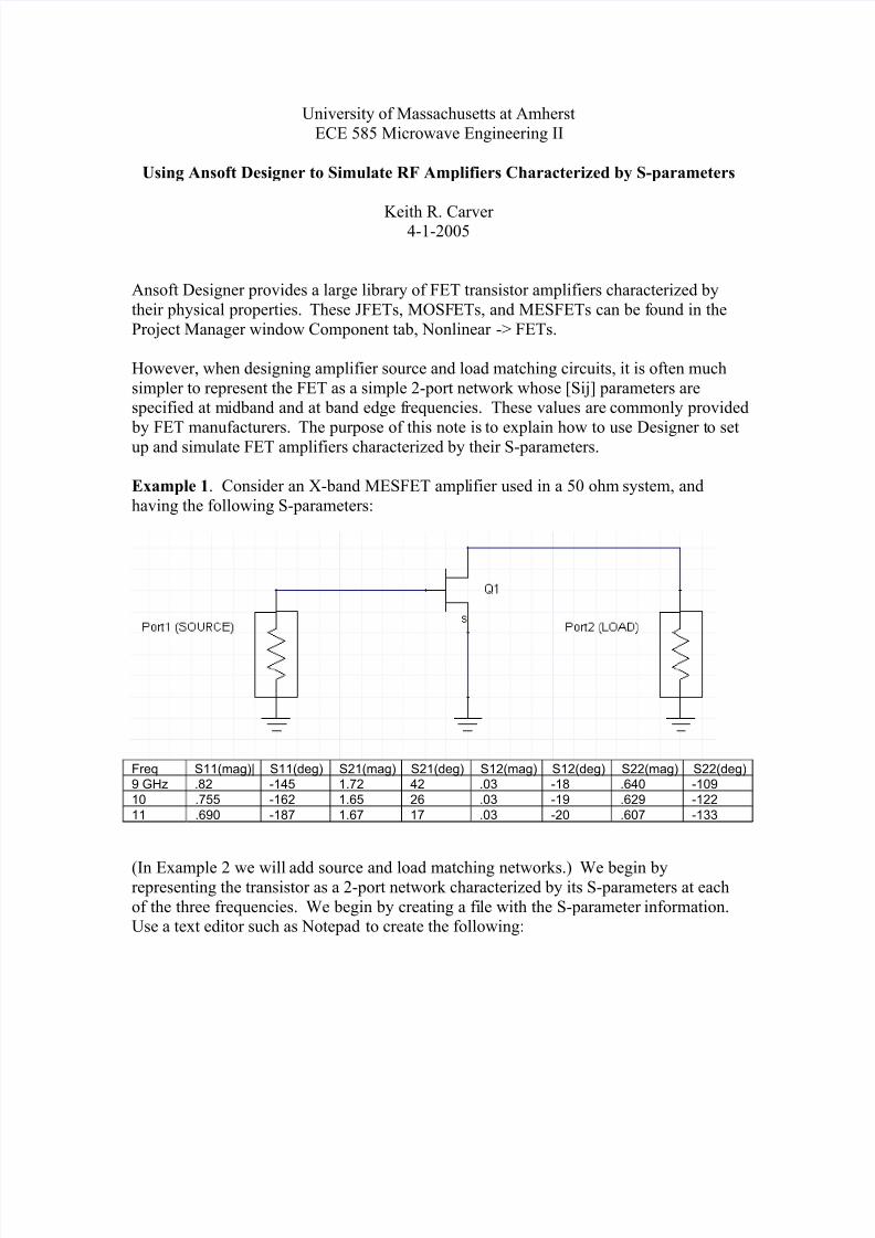
Example 1. Consider an X-band MESFET amplifier used in a 50 ohm system, and
having the following S-parameters:
Freq S11(mag)| S11(deg) S21(mag) S21(deg) S12(mag) S12(deg) S22(mag) S22(deg)
9 GHz .82 -145 1.72 42 .03 -18 .640 -109
10 .755 -162 1.65 26 .03 -19 .629 -122
11 .690 -187 1.67 17 .03 -20 .607 -133
(In Example 2 we will add source and load matching networks.) We begin byrepresenting the transistor as a 2-port network characterized by its S-parameters at each
of the three frequencies. We begin by creating a file with the S-parameter information.Use a text editor such as Notepad to create the following:
8/14/2019 Dsgnr Tutorial FETs 2ports
http://slidepdf.com/reader/full/dsgnr-tutorial-fets-2ports 2/6
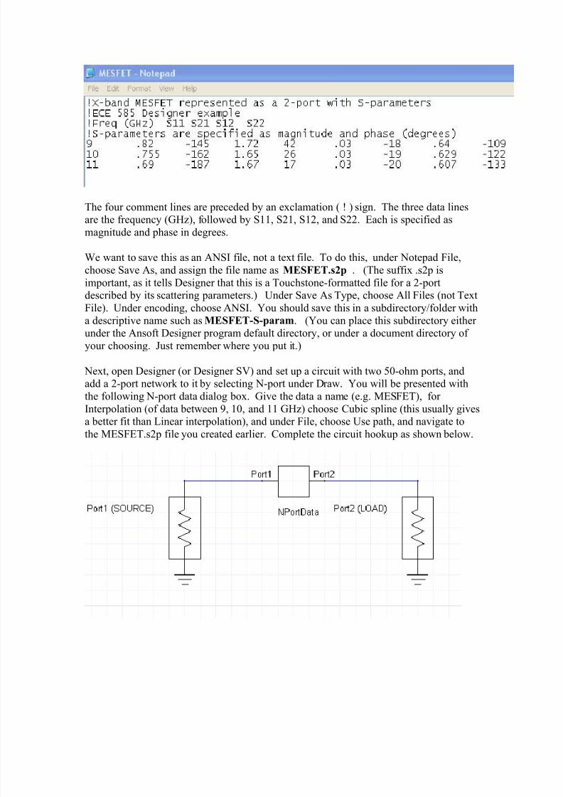
The four comment lines are preceded by an exclamation ( ! ) sign. The three data linesare the frequency (GHz), followed by S11, S21, S12, and S22. Each is specified as
magnitude and phase in degrees.
We want to save this as an ANSI file, not a text file. To do this, under Notepad File,
choose Save As, and assign the file name as MESFET.s2p . (The suffix .s2p is
important, as it tells Designer that this is a Touchstone-formatted file for a 2-portdescribed by its scattering parameters.) Under Save As Type, choose All Files (not Text
File). Under encoding, choose ANSI. You should save this in a subdirectory/folder with
a descriptive name such as MESFET-S-param. (You can place this subdirectory either under the Ansoft Designer program default directory, or under a document directory of
your choosing. Just remember where you put it.)
Next, open Designer (or Designer SV) and set up a circuit with two 50-ohm ports, andadd a 2-port network to it by selecting N-port under Draw. You will be presented with
the following N-port data dialog box. Give the data a name (e.g. MESFET), for
Interpolation (of data between 9, 10, and 11 GHz) choose Cubic spline (this usually gives
a better fit than Linear interpolation), and under File, choose Use path, and navigate tothe MESFET.s2p file you created earlier. Complete the circuit hookup as shown below.
8/14/2019 Dsgnr Tutorial FETs 2ports
http://slidepdf.com/reader/full/dsgnr-tutorial-fets-2ports 3/6
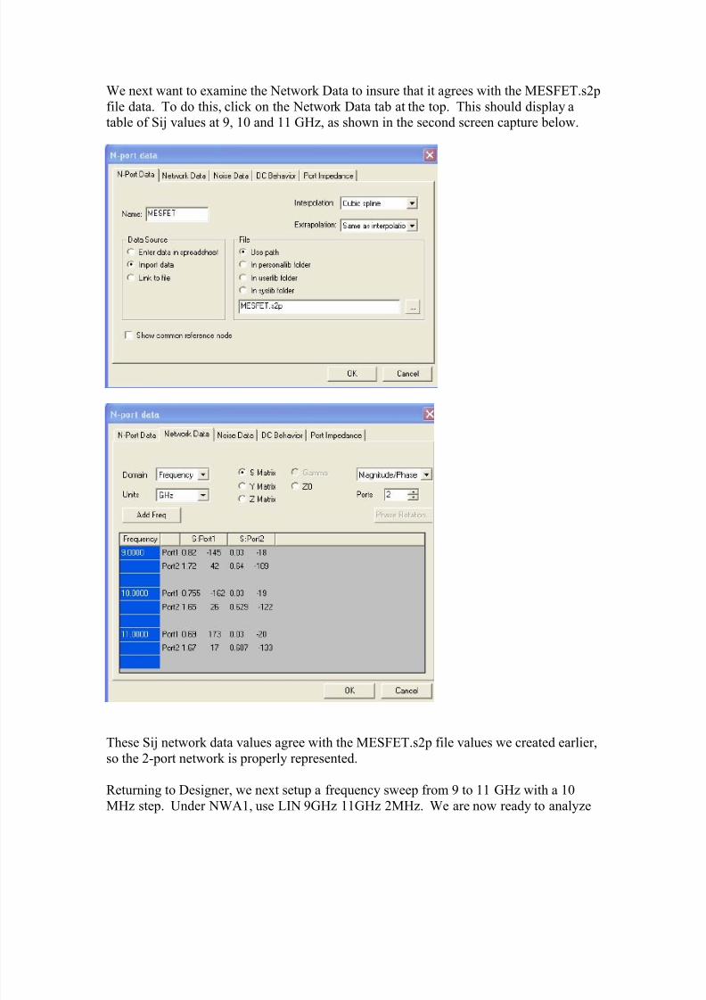
We next want to examine the Network Data to insure that it agrees with the MESFET.s2p
file data. To do this, click on the Network Data tab at the top. This should display atable of Sij values at 9, 10 and 11 GHz, as shown in the second screen capture below.
These Sij network data values agree with the MESFET.s2p file values we created earlier,
so the 2-port network is properly represented.
Returning to Designer, we next setup a frequency sweep from 9 to 11 GHz with a 10
MHz step. Under NWA1, use LIN 9GHz 11GHz 2MHz. We are now ready to analyze
8/14/2019 Dsgnr Tutorial FETs 2ports
http://slidepdf.com/reader/full/dsgnr-tutorial-fets-2ports 4/6
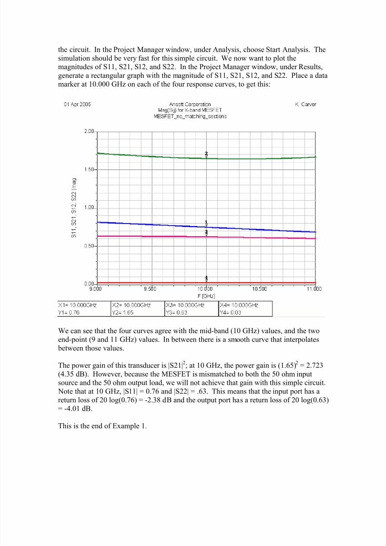
the circuit. In the Project Manager window, under Analysis, choose Start Analysis. The
simulation should be very fast for this simple circuit. We now want to plot themagnitudes of S11, S21, S12, and S22. In the Project Manager window, under Results,
generate a rectangular graph with the magnitude of S11, S21, S12, and S22. Place a data
marker at 10.000 GHz on each of the four response curves, to get this:
We can see that the four curves agree with the mid-band (10 GHz) values, and the two
end-point (9 and 11 GHz) values. In between there is a smooth curve that interpolates
between those values.
The power gain of this transducer is |S21|2; at 10 GHz, the power gain is (1.65)
2= 2.723
(4.35 dB). However, because the MESFET is mismatched to both the 50 ohm input
source and the 50 ohm output load, we will not achieve that gain with this simple circuit. Note that at 10 GHz, |S11| = 0.76 and |S22| = .63. This means that the input port has a
return loss of 20 log(0.76) = -2.38 dB and the output port has a return loss of 20 log(0.63)= -4.01 dB.
This is the end of Example 1.
8/14/2019 Dsgnr Tutorial FETs 2ports
http://slidepdf.com/reader/full/dsgnr-tutorial-fets-2ports 5/6
Example 2. We now add two simple matching circuits to our X-band MESFET
amplifier, one at the source and the other at the load. Each matching circuit is a single-stub tuner using 50-ohm lines. Both stubs are open-circuited.
This design (discussed in the lecture notes) provides an overall power gain at midband of
7.4 dB at 10 GHz and a broadband gain response (little variation in S21 over the 9 – 11
GHz range). At midband, the source (port 1) matching network has a gain of 2 dB, andthe load (port 2) matching network has a gain of 1 dB. When added to the 4.35 dB gain
of the transistor, the overall midband power gain is 7.35 dB.
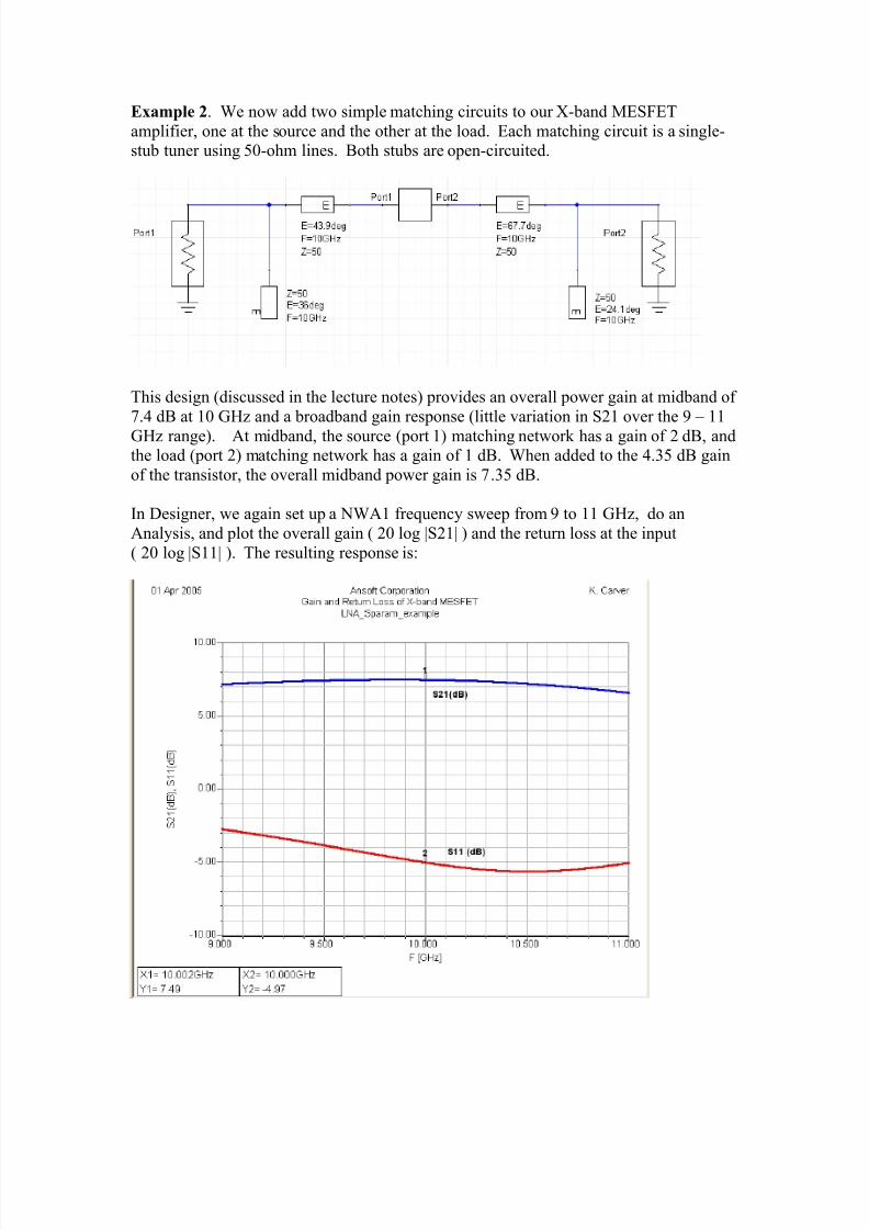
In Designer, we again set up a NWA1 frequency sweep from 9 to 11 GHz, do an
Analysis, and plot the overall gain ( 20 log |S21| ) and the return loss at the input
( 20 log |S11| ). The resulting response is:

8/14/2019 Dsgnr Tutorial FETs 2ports
http://slidepdf.com/reader/full/dsgnr-tutorial-fets-2ports 6/6
The simulated midband gain of the amplifier is 7.5 dB, with little variation over the 9 – 11 GHz. At 11 GHz, the gain drops to 6.8 dB. However, the return loss is rather poor,
especially at 9 GHz (-2.9 dB). If we change the matching circuits to provide maximum
gain at midband, and give up some bandwidth, we can greatly improve the midband
return loss. This is discussed in the lecture notes.
This is the end of Example 2.