Embed Size (px)
Citation preview
c
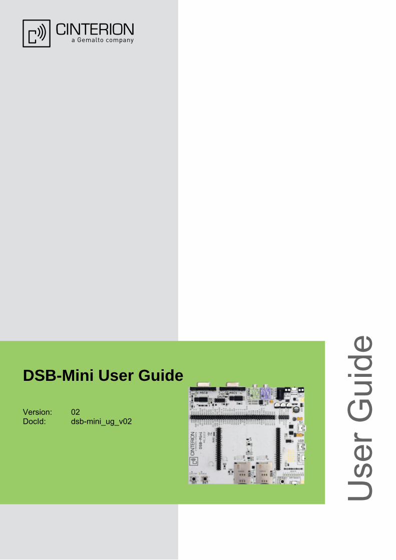
DSB-Mini User Guide
Version: 02DocId: dsb-mini_ug_v02
Use
r G
uide
GENERAL NOTE THE USE OF THE PRODUCT INCLUDING THE SOFTWARE AND DOCUMENTATION (THE "PROD-UCT") IS SUBJECT TO THE RELEASE NOTE PROVIDED TOGETHER WITH PRODUCT. IN ANYEVENT THE PROVISIONS OF THE RELEASE NOTE SHALL PREVAIL. THIS DOCUMENT CON-TAINS INFORMATION ON CINTERION PRODUCTS. THE SPECIFICATIONS IN THIS DOCUMENTARE SUBJECT TO CHANGE AT CINTERION'S DISCRETION. CINTERION WIRELESS MODULESGMBH GRANTS A NON-EXCLUSIVE RIGHT TO USE THE PRODUCT. THE RECIPIENT SHALL NOTTRANSFER, COPY, MODIFY, TRANSLATE, REVERSE ENGINEER, CREATE DERIVATIVE WORKS;DISASSEMBLE OR DECOMPILE THE PRODUCT OR OTHERWISE USE THE PRODUCT EXCEPTAS SPECIFICALLY AUTHORIZED. THE PRODUCT AND THIS DOCUMENT ARE PROVIDED ON AN"AS IS" BASIS ONLY AND MAY CONTAIN DEFICIENCIES OR INADEQUACIES. TO THE MAXIMUMEXTENT PERMITTED BY APPLICABLE LAW, CINTERION WIRELESS MODULES GMBH DIS-CLAIMS ALL WARRANTIES AND LIABILITIES. THE RECIPIENT UNDERTAKES FOR AN UNLIMITEDPERIOD OF TIME TO OBSERVE SECRECY REGARDING ANY INFORMATION AND DATA PRO-VIDED TO HIM IN THE CONTEXT OF THE DELIVERY OF THE PRODUCT. THIS GENERAL NOTESHALL BE GOVERNED AND CONSTRUED ACCORDING TO GERMAN LAW.
CopyrightTransmittal, reproduction, dissemination and/or editing of this document as well as utilization of its con-tents and communication thereof to others without express authorization are prohibited. Offenders willbe held liable for payment of damages. All rights created by patent grant or registration of a utility modelor design patent are reserved.
Copyright © 2012, Cinterion Wireless Modules GmbH
Trademark NoticeMicrosoft and Windows are either registered trademarks or trademarks of Microsoft Corporation in theUnited States and/or other countries. All other registered trademarks or trademarks mentioned in thisdocument are property of their respective owners.
dsb-mini_ug_v02 Page 2 of 30 2012-10-09Confidential / Released
DSB-Mini User Guide c
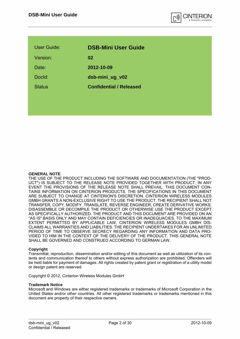
User Guide: DSB-Mini User Guide
Version: 02
Date: 2012-10-09
DocId: dsb-mini_ug_v02
Status Confidential / Released
DSB-Mini User Guide Contents30
c
dsb-mini_ug_v02 Page 3 of 30 2012-10-09Confidential / Released
Contents
0 Document History ...................................................................................................... 6
1 Introduction ................................................................................................................. 71.1 Regulatory Compliance Information................................................................... 71.2 Supported Products ........................................................................................... 71.3 Related Documents ........................................................................................... 71.4 Scope of delivery ............................................................................................... 8
2 Product Concept ......................................................................................................... 92.1 Key Features at a Glance ................................................................................ 102.2 System Overview ............................................................................................. 11
3 Interface Description ................................................................................................ 123.1 Power Supply................................................................................................... 12
3.1.1 Power Path Switch.............................................................................. 123.2 Serial Communication Interfaces ..................................................................... 133.3 Analog Audio Interface..................................................................................... 143.4 SIM Interface.................................................................................................... 14
3.4.1 Automatic Dual SIM Operation ........................................................... 143.4.2 CCVCC Adjustment ............................................................................ 153.4.3 Component SIM Card Support............................................................ 15
3.5 Status LEDs ..................................................................................................... 153.6 Application Connectors .................................................................................... 16
3.6.1 2x40-Pin Connector for Starter Kits .................................................... 163.6.2 80-Pin Connector for DSB75 Module Adapters .................................. 213.6.3 10-Pin Digital Audio Connector........................................................... 223.6.4 10-Pin Connector for Starter Kit Signals ............................................. 22
3.7 Patch Field ....................................................................................................... 23
4 Appendix: Schematics and Placement ................................................................... 24
DSB-Mini User Guide Tables30
c
dsb-mini_ug_v02 Page 4 of 30 2012-10-09Confidential / Released
Tables
Table 1: DSB-Mini delivery package.............................................................................. 8Table 2: Key features at a glance ................................................................................ 10Table 3: Automatic dual SIM operation ........................................................................ 14Table 4: CCVCC adjustment........................................................................................ 15Table 5: Status LEDs ................................................................................................... 15Table 6: 2x40 pin connector pin assignment................................................................ 16Table 7: 2x40-pin connector pin description and mapping........................................... 17Table 8: 80-pin connector pin assignment ................................................................... 21Table 9: 10-pin digital audio connector ........................................................................ 22Table 10: 10-pin connector for additional Starter Kit signals.......................................... 22
DSB-Mini User Guide Figures30
c
dsb-mini_ug_v02 Page 5 of 30 2012-10-09Confidential / Released
Figures
Figure 1: DSB-Mini overview........................................................................................... 9Figure 2: DSB-Mini system overview ............................................................................ 11Figure 3: Schematics, Page 1 ....................................................................................... 24Figure 4: Schematics, Page 2 ....................................................................................... 25Figure 5: Schematics, Page 3 ....................................................................................... 26Figure 6: Schematics, Page 4 ....................................................................................... 27Figure 7: Schematics, Page 5 ....................................................................................... 28Figure 8: Placement, Page 1 (top) ................................................................................ 29Figure 9: Placement, Page 2 (with Starter Kit mounted) ............................................... 30

DSB-Mini User Guide0 Document History6
c
dsb-mini_ug_v02 Page 6 of 30 2012-10-09Confidential / Released
0 Document History
Preceding document: "DSB-Mini User Guide" Version 01New document: "DSB-Mini User Guide" Version 02
New document: "DSB-Mini User Guide" Version 01
Chapter What is new
1.1 New section Regulatory Compliance Information.
Chapter What is new
--- Initial document setup.
DSB-Mini User Guide1 Introduction23
c
dsb-mini_ug_v02 Page 7 of 30 2012-10-09Confidential / Released
1 Introduction
The DSB-Mini is a simple and easy-to-use development support board, designed to assist sys-tem integrators in developing and evaluating products based on Cinterion Wireless Modules.
This document describes all interfaces of the DSB-Mini, provides technical specifications andpresents guidelines for connecting and operating the Cinterion modules to be evaluated.
Chapter 2 introduces the product concept, including key features and system overview, Chap-ter 3 describes the DSB-Mini’s interfaces in some more detail including the DSB-Mini’s connec-tor pin assignments. The Appendix finally contains schematics and placement (see Chapter 4).
1.1 Regulatory Compliance Information
The DSB-Mini is intended for use only in a laboratory test environment. All persons handlingthe DSB-Mini must be properly trained in electronics and observe good engineering practicestandards.
The DSB-Mini is a test/development platform and has not been designed to be embedded intoother products (referred as "final products").
The DSB-Mini is not intended for use as reference environment for type approval.
1.2 Supported Products
The DSB-Mini provides two 40-pin connectors to mount the Cinterion Starter Kits B60 and B80in order to evaluate the full functionality of modules that can be connected to these Starter Kits.Also, the DSB-Mini has an 80-pin connector to mount the Cinterion Multi-Adapter R1 or variousother DSB75 product adapter together with their plugged modules. Signals and levels are ineach case switched automatically.
The diversity of the supported products implies that, due to hardware or software specific prop-erties, major differences occur regarding the availability of interfaces and the implementationof features. Therefore, please consult the specifications supplied with your module, especially[1] and [2], to make sure whether or not a described interface, signal, operating mode or func-tion offered by the DSB75 is supported.
1.3 Related Documents
[1] AT Command Set for the appropriate module[2] Hardware Interface Description for the appropriate module[3] DSB75 Development Support Board Rev. B1 Hardware Description [4] Starter Kit B60 User Guide[5] Starter Kit B80 User Guide
DSB-Mini User Guide1.4 Scope of delivery23
c
dsb-mini_ug_v02 Page 8 of 30 2012-10-09Confidential / Released
1.4 Scope of delivery
The Cinterion modules, Starter Kits and DSB75 module adapter for use with the DSB-Mini arenot included in the scope of delivery.
Table 1: DSB-Mini delivery package
Quantity Description
1 DSB-Mini
DSB-Mini User Guide2 Product Concept23
c
dsb-mini_ug_v02 Page 9 of 30 2012-10-09Confidential / Released
2 Product Concept
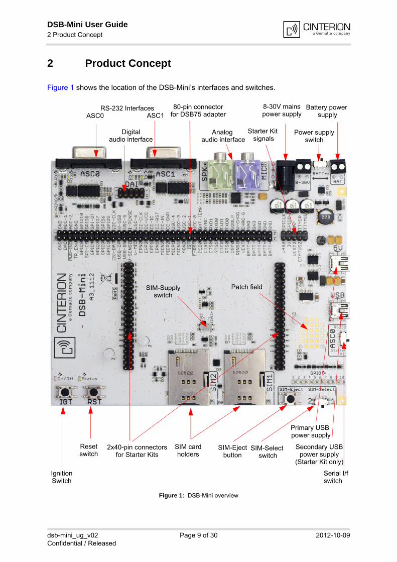
Figure 1 shows the location of the DSB-Mini’s interfaces and switches.
Figure 1: DSB-Mini overview
8-30V mains Battery power
Power supply
RS-232 Interfaces
Analog
Ignition
SIM card SIM-Eject SIM-SelectReset
ASC0 ASC1 supply
switch
power supply
Switch
switch buttonholders
Primary USB
Secondary USB
Serial I/f
80-pin connector
2x40-pin connectors
switch
for DSB75 adapter
for Starter Kits
power supply
power supply(Starter Kit only)
Digitalaudio interface audio interface
Starter Kit signals
switch
SIM-Supplyswitch
Patch field
DSB-Mini User Guide2.1 Key Features at a Glance23
c
dsb-mini_ug_v02 Page 10 of 30 2012-10-09Confidential / Released
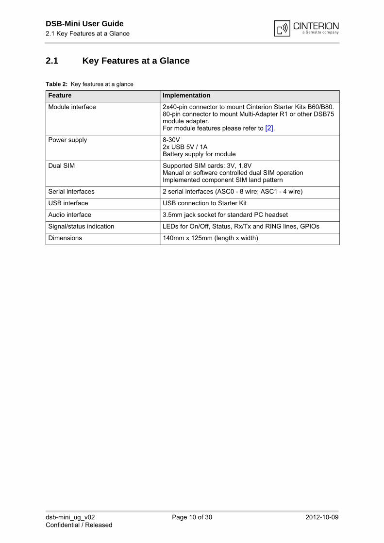
2.1 Key Features at a Glance
Table 2: Key features at a glance
Feature Implementation
Module interface 2x40-pin connector to mount Cinterion Starter Kits B60/B80.80-pin connector to mount Multi-Adapter R1 or other DSB75 module adapter. For module features please refer to [2].
Power supply 8-30V2x USB 5V / 1ABattery supply for module
Dual SIM Supported SIM cards: 3V, 1.8VManual or software controlled dual SIM operationImplemented component SIM land pattern
Serial interfaces 2 serial interfaces (ASC0 - 8 wire; ASC1 - 4 wire)
USB interface USB connection to Starter Kit
Audio interface 3.5mm jack socket for standard PC headset
Signal/status indication LEDs for On/Off, Status, Rx/Tx and RING lines, GPIOs
Dimensions 140mm x 125mm (length x width)
DSB-Mini User Guide2.2 System Overview23
c
dsb-mini_ug_v02 Page 11 of 30 2012-10-09Confidential / Released
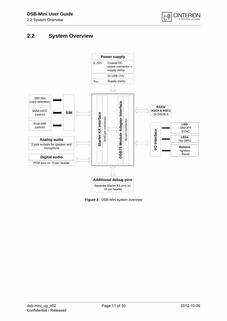
2.2 System Overview
Figure 2: DSB-Mini system overview
Sta
rter
Kit
inte
rfac
e2x
40
pin
con
nect
or
SIM
SIM Slot(card detection)
M2M-UICC(option)
Dual-SIM(option)
RS232ASC0 & ASC1
2x DSUB-9
Buttons-Ignition- Reset
I/O
In
terf
ac
e
LED- ON/OFF- SYNC
LEDs10x GPIO
Power supply
8..30V Coaxial DC power connector +
supply clamp
2x USB (1A)
Vbatt Supply clamp
DS
B75
Mo
du
le A
da
pte
r In
terf
ace
80-p
in c
onne
cto
r
Digital audio
PCM pins on 10-pin header
Analog audio2 jack sockets for speaker and
microphone
Additional debug pins
Separate Starter Kit pins on 10-pin header
DSB-Mini User Guide3 Interface Description23
c
dsb-mini_ug_v02 Page 12 of 30 2012-10-09Confidential / Released
3 Interface Description
3.1 Power Supply
To operate the DSB-Mini (including a connected module) a constant voltage supply is required.The following power supply sources may be employed:
• 8-30V mains adapterProvides the main power supply for all DSB-Mini functions. An internal DC/DC switchingregulator adjusts the voltage down to 5V. Allows common 12V mains supplies and thereforethe usage in a car environment for example. A coaxial power connector allows for plugs withcommon 2.1mm or 2.5mm inside parameters. A reverse polarity protection is included for8-30V.Note: The power supply path does not include a short circuit protection. For usage in a carenvironment for example the main power supply 8-30V will have to be additionally fused by1A to prevent overcurrent in case of shorting the 5V or module power supply.
• 5V USB power supplyThe USB power source provides the main power supply for all DSB-Mini functions. A sep-arate external mains supply is not necessarily required. Power can be derived from the two USB interfaces (5V / 1A) - the primary USB power sup-ply connector labelled "5V" and the secondary connector labelled "USB". Generally, it isrecommended to use both connectors for power supply - unless power consumption is quitelow because the RF interface is not being used or only at lower multislot classes with verygood reception quality. However, the use of both USB power supply connectors is supported for the Starter Kit only.If employing module adapters on the 80-pin connector (e.g. the Multi-Adapter R1), only theprimary USB power supply connector delivers the power (i.e., 500mA). In this case a USBY-cable at the primary USB connector or the mains supply 8-30V will have to be employedin addition to the primary USB connector in order to compensate for a possible increasedcurrent consumption during radio transmissions at higher multislot classes.
• Battery power supplyProvides for a separate power supply source for the module - such as a battery. If the bat-tery power supply is used for the module, either the 8-30V power supply source or the 5VUSB power supply source is required to operate the remaining DSB-Mini functions. Acharging funtionality is not supported.
3.1.1 Power Path Switch
The DSB-Mini has a switch ("BATT+") to select the module’s power supply path: • 8-30V
The DSB-Mini is supplied with 5V derived from the 8-30V mains adapter or the 5V USBpower supply (see Section 3.1). A post LDO regulates this voltage down to 3.7V to supplythe module on the Starter Kit or DSB75 adapter.
• BATOnly if the module connected to the Starter Kit or DSB75 module adapter is supplied froman external battery should this switch be set to "BAT".
DSB-Mini User Guide3.2 Serial Communication Interfaces23
c
dsb-mini_ug_v02 Page 13 of 30 2012-10-09Confidential / Released
3.2 Serial Communication Interfaces
The DSB-Mini has two RS-232 interfaces to communicate with the module’s serial interfacesASC0 and ASC1. ASC0 is a full 8-wire UART interface, while ASC1 is a 4-wire UART interface.
If the DSB-Mini is employed together with an adapter like the Multi-Adapter R1 or any otherDSB75 module adapter, the RS-232 interfaces (ASC0, ASC1) on the DSB-Mini are automati-cally enabled and can be used.
However, if the DSB-Mini is used together with a Starter Kit, the switch ("ASC0") has to be setto select whether to use the RS-232 interface on the DSB-Mini or the USB-to-UART bridge onthe Starter Kit for ASC0 communication: • RS232
If set to "RS232" the module communicates via the RS-232 interfaces on the DSB-Mini. TheUSB-to-UART bridge on the Starter Kit is reset and releases all ASC0 serial signals.
• Starter KitIf set to "Starter Kit" the module’s ASC0 interface communicates via the USB-to-UARTbridge of the Starter Kit. In this case the RS-232 level shifter on the DSB-Mini releases allASC0 serial signals. For more information on the USB-to-UART bridge please refer to theappropriate Starter Kit documentation ([4] or [5]).
DSB-Mini User Guide3.3 Analog Audio Interface23
c
dsb-mini_ug_v02 Page 14 of 30 2012-10-09Confidential / Released
3.3 Analog Audio Interface
A standard PC headset can be connected via the two 3.5mm jack sockets (SPK=Speaker,MIC=Microphone).
3.4 SIM Interface
The DSB-Mini has a dual SIM interface and provides two SIM card holders or alternatively twoland patterns for component SIMs to be soldered. The "SIM-Select" switch can be used tospecify the active SIM card. An LED will indicate this SIM card. The SIM card holder supportsSIM removal detection.
To manually switch between two inserted SIM cards during module operation please completethe following steps:• Press and hold the "SIM-Eject" button. This simulates the CCIN signal, indicating to the
module that the SIM card has been removed.• Set the "SIM-Select" switch to configure the active SIM card ("1" or "2"). • Release the "SIM-Eject" button to indicate to the module to restart the SIM software stack
and to activate the selected SIM card.
Please note that a combined operation with SIM cards inserted on both the Starter Kit and theDSB-Mini is not supported.
3.4.1 Automatic Dual SIM Operation
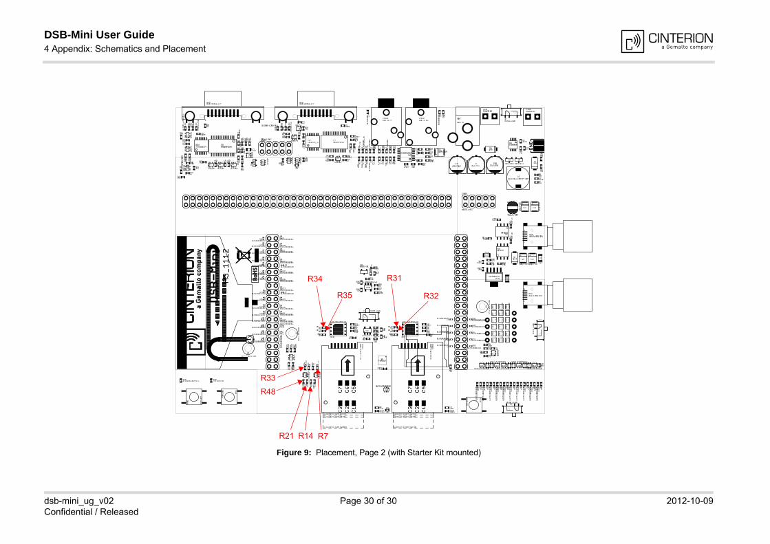
To automatically control dual SIM operation, it is necessary to complete the same steps as de-scribed above for the manual switch. To do this the two internal signals SIM_SELECT ("SIM-Select" switch) and CCEJECT ("SIM-Eject" button) will have to be connected to the GPIO1 andGPIO2 signals by removing resistor R21 (0) and placing 0 resistors for R7 and R14 (for de-tails see Appendix: Figure 6 and Figure 9).
The following functionality then applies for GPIO1 and GPIO2:
Having assigned the internal signals to the GPIO signals it is now possible to change the activeSIM card by automatically completing the steps described above for the manual control. TheGPIO signals can be configured and controlled by means of AT commands.
Table 3: Automatic dual SIM operation
Module signal Function Modification Description
GPIO1 CCSELECT("SIM-Select")
Place R14/0Ω instead of R21/0Ω
Select SIM1 or SIM2Low: SIM1High: SIM2
GPIO2 CCEJECT("SIM-Eject")
Place R7/0Ω Eject the SIMLow: SIM inserted (47k pull-down)High: SIM ejected
DSB-Mini User Guide3.5 Status LEDs23
c
dsb-mini_ug_v02 Page 15 of 30 2012-10-09Confidential / Released
3.4.2 CCVCC Adjustment
By default, the "SIM-Supply" switch is set to "CCVCC" and should remain as such, meaningthat CCVCC is delivered from the module.
In some cases however, employing the dual SIM feature may require a slightly higher supplylevel to compensate for possible voltage drops. This can be achieved by setting the "SIM-Sup-ply" switch to "CCVCC+". The SIM supply voltage is then increased by 5%.
3.4.3 Component SIM Card Support
The DSB-Mini provides two land patterns for an optional use of component UICCs (SIM/USIM/MIM). It is possible to solder UICCs for single card or dual card operation. Depending on themanufacturer and package of the used UICC, pin 6 or pin 7 is used for the I/O line. Thus it isnecessary to place a 0Ohm resistor either for R31 or R32 for SIM 1, and a 0Ohm resistor foreither R34 or R35 for SIM 2. Please refer to the package specification of the UICC as well asto the Appendix: Figure 6 and Figure 9.
It is also necessary to place a 47kOhm resistor as R48 for SIM 1 and a respective 47kOhmresistor as R33 for SIM 2 to bypass the SIM card detection (see Appendix: Figure 6 and Figure9). Component SIMs are always inserted.
3.5 Status LEDs
The DSB-Mini comprises a number of status LEDs for various module features. The LEDs aremarked on the DSB-Mini board with arrows pointing upwards (led).
Table 4: CCVCC adjustment
Switch setting CCVCC supply voltage
“CCVCC” CCVCC (from module)
“CCVCC+” CCVCC + 5%
Table 5: Status LEDs
Feature Description
On / Off LED indicates On state of module
Status LED indicates operating modes of the module
SIM 1 / 2 LED indicates active SIM card
RX / TX for ASC0 LED indicates RX/TX traffic over ASC0
RX / TX for ASC1 LED indicates RX/TX traffic over ASC1
RING LED indicates incoming calls and URCs
GPIO 1...10 LED indicates status of GPIO lines
DSB-Mini User Guide3.6 Application Connectors23
c
dsb-mini_ug_v02 Page 16 of 30 2012-10-09Confidential / Released
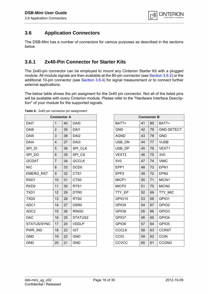
3.6 Application Connectors
The DSB-Mini has a number of connectors for various purposes as described in the sectionsbelow.
3.6.1 2x40-Pin Connector for Starter Kits
The 2x40-pin connector can be employed to mount any Cinterion Starter Kit with a pluggedmodule. All module signals are then available at the 80-pin connector (see Section 3.6.2) or theadditional 10-pin connector (see Section 3.6.4) for signal measurement or to connect furtherexternal applications.
The below table shows the pin assigment for the 2x40 pin connector. Not all of the listed pinswill be available with every Cinterion module. Please refer to the "Hardware Interface Descrip-tion" of your module for the supported signals.
Table 6: 2x40 pin connector pin assignment
Connector A Connector B
DAI7 1 40 DAI0 BATT+ 41 80 BATT+
DAI6 2 39 DAI1 GND 42 79 GND.DETECT
DAI5 3 38 DAI2 AGND 43 78 GND
DAI4 4 37 DAI3 USB_DN 44 77 VUSB
SPI_DI 5 36 SPI_CLK USB_DP 45 76 VEXT1
SPI_DO 6 35 SPI_CS VEXT2 46 75 3V0
I2CDAT 7 34 I2CCLK 5V0 47 74 VMIC
N/C 8 33 DCD0 EPP1 48 73 EPN1
EMERG_RST 9 32 CTS1 EPP2 49 72 EPN2
RXD1 10 31 CTS0 MICP1 50 71 MICN1
RXD0 11 30 RTS1 MICP2 51 70 MICN2
TXD1 12 29 DTR0 TTY_EP 52 69 TTY_MIC
TXD0 13 28 RTS0 GPIO10 53 68 GPIO1
ADC1 14 27 DSR0 GPIO9 54 67 GPIO2
ADC2 15 26 RING0 GPIO8 55 66 GPIO3
DAC 16 25 STATUS2 GPIO7 56 65 GPIO4
STATUS/SYNC 17 24 VDDLP GPIO6 57 64 GPIO5
PWR_IND 18 23 IGT CCCLK 58 63 CCRST
GND 19 22 GND CCIO 59 62 CCIN
GND 20 21 GND CCVCC 60 61 CCGND
DSB-Mini User Guide3.6 Application Connectors23
c
dsb-mini_ug_v02 Page 17 of 30 2012-10-09Confidential / Released
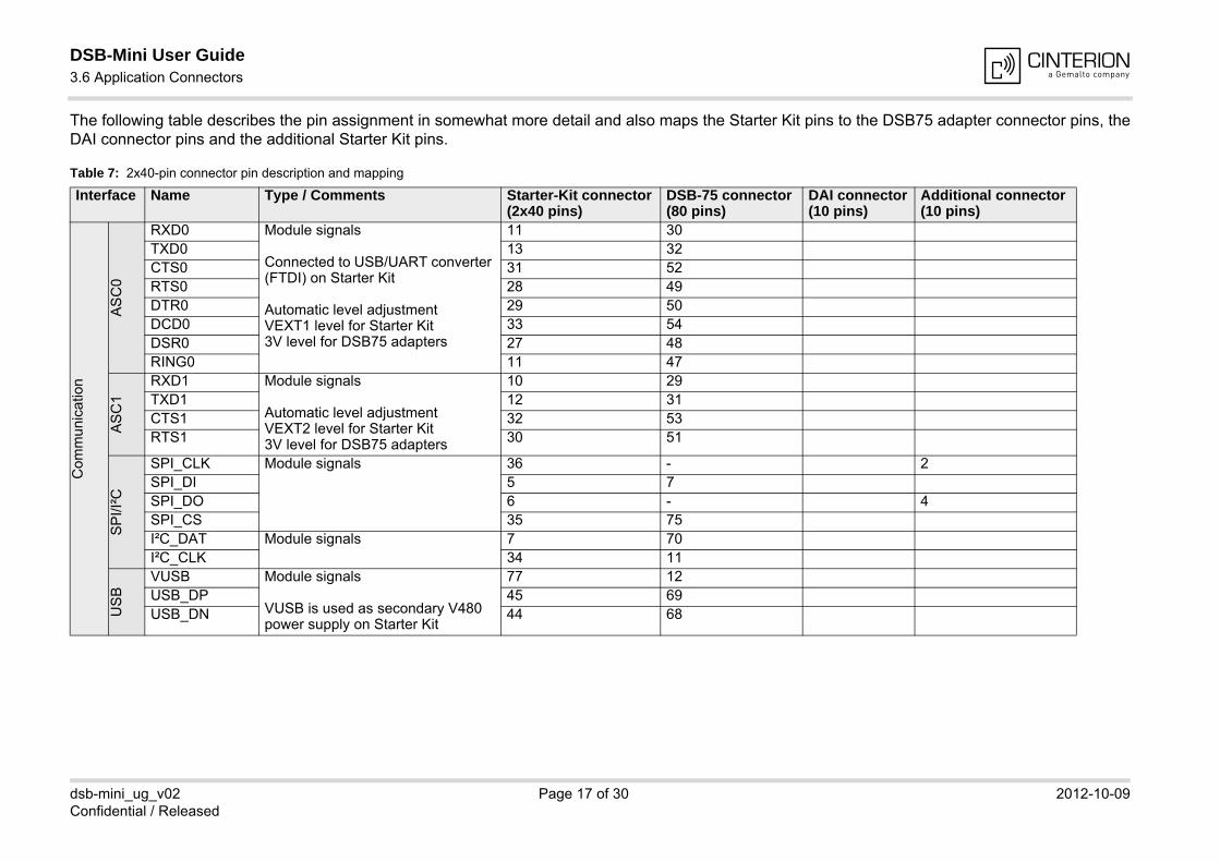
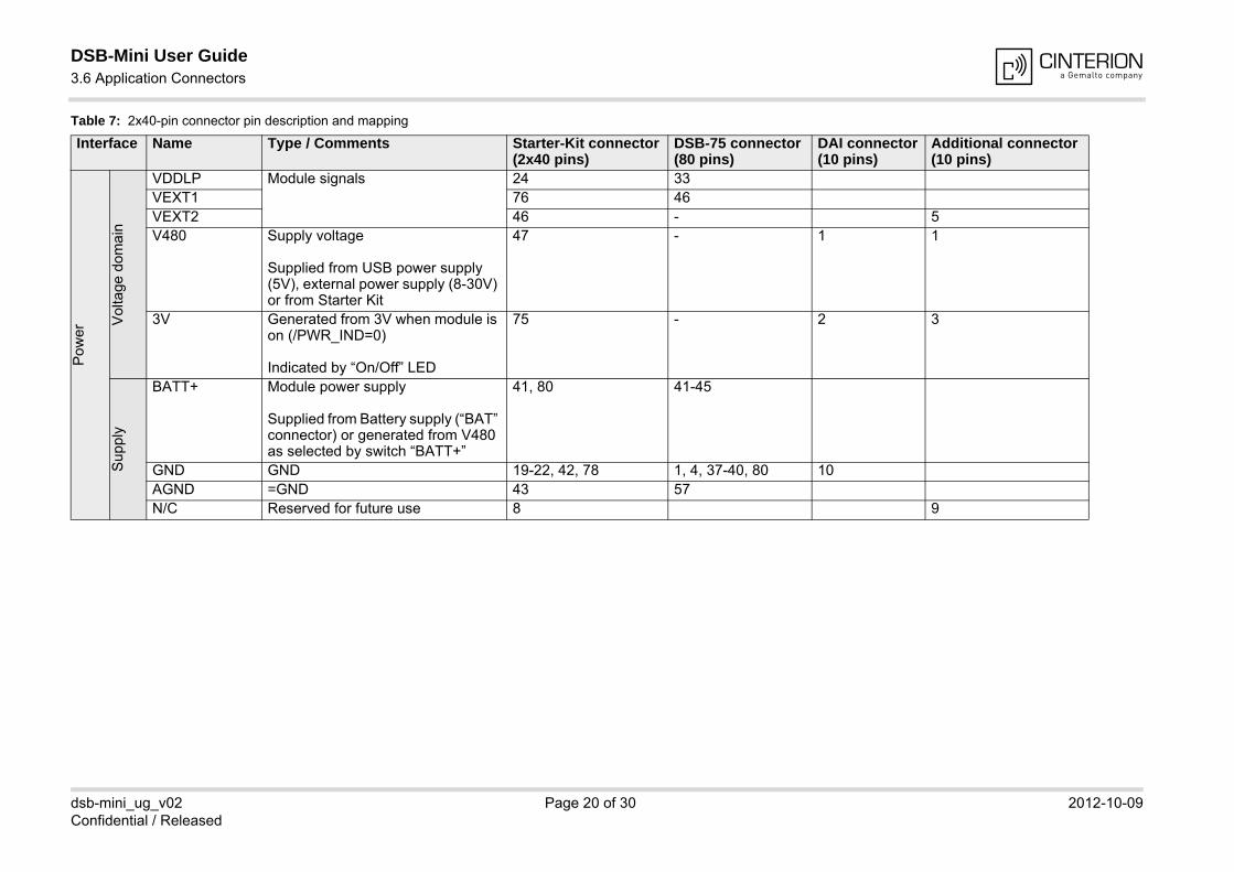
The following table describes the pin assignment in somewhat more detail and also maps the Starter Kit pins to the DSB75 adapter connector pins, theDAI connector pins and the additional Starter Kit pins.
Table 7: 2x40-pin connector pin description and mapping
Interface Name Type / Comments Starter-Kit connector(2x40 pins)
DSB-75 connector(80 pins)
DAI connector(10 pins)
Additional connector(10 pins)
Co
mm
un
icat
ion
AS
C0
RXD0 Module signals
Connected to USB/UART converter (FTDI) on Starter Kit
Automatic level adjustmentVEXT1 level for Starter Kit3V level for DSB75 adapters
11 30TXD0 13 32CTS0 31 52RTS0 28 49DTR0 29 50DCD0 33 54DSR0 27 48RING0 11 47
AS
C1
RXD1 Module signals
Automatic level adjustmentVEXT2 level for Starter Kit3V level for DSB75 adapters
10 29TXD1 12 31CTS1 32 53RTS1 30 51
SP
I/I²C
SPI_CLK Module signals 36 - 2SPI_DI 5 7SPI_DO 6 - 4SPI_CS 35 75I²C_DAT Module signals 7 70I²C_CLK 34 11
US
B
VUSB Module signals
VUSB is used as secondary V480 power supply on Starter Kit
77 12USB_DP 45 69USB_DN 44 68
DSB-Mini User Guide3.6 Application Connectors23
c
dsb-mini_ug_v02 Page 18 of 30 2012-10-09Confidential / Released
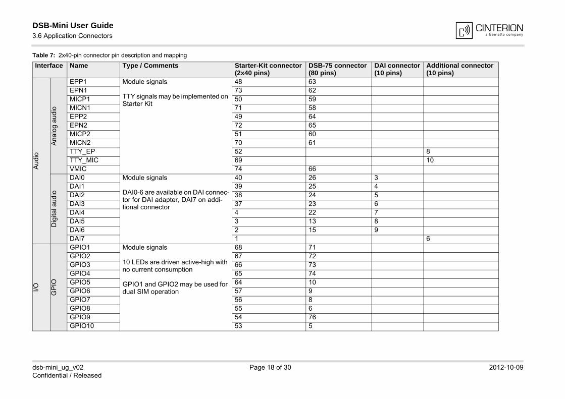
Aud
io
An
alo
g a
udio
EPP1 Module signals
TTY signals may be implemented on Starter Kit
48 63EPN1 73 62MICP1 50 59MICN1 71 58EPP2 49 64EPN2 72 65MICP2 51 60MICN2 70 61TTY_EP 52 8TTY_MIC 69 10VMIC 74 66
Dig
ital a
udio
DAI0 Module signals
DAI0-6 are available on DAI connec-tor for DAI adapter, DAI7 on addi-tional connector
40 26 3DAI1 39 25 4DAI2 38 24 5DAI3 37 23 6DAI4 4 22 7DAI5 3 13 8DAI6 2 15 9DAI7 1 6
I/O
GP
IO
GPIO1 Module signals
10 LEDs are driven active-high with no current consumption
GPIO1 and GPIO2 may be used for dual SIM operation
68 71GPIO2 67 72GPIO3 66 73GPIO4 65 74GPIO5 64 10GPIO6 57 9GPIO7 56 8GPIO8 55 6GPIO9 54 76GPIO10 53 5
Table 7: 2x40-pin connector pin description and mapping
Interface Name Type / Comments Starter-Kit connector(2x40 pins)
DSB-75 connector(80 pins)
DAI connector(10 pins)
Additional connector(10 pins)
DSB-Mini User Guide3.6 Application Connectors23
c
dsb-mini_ug_v02 Page 19 of 30 2012-10-09Confidential / Released
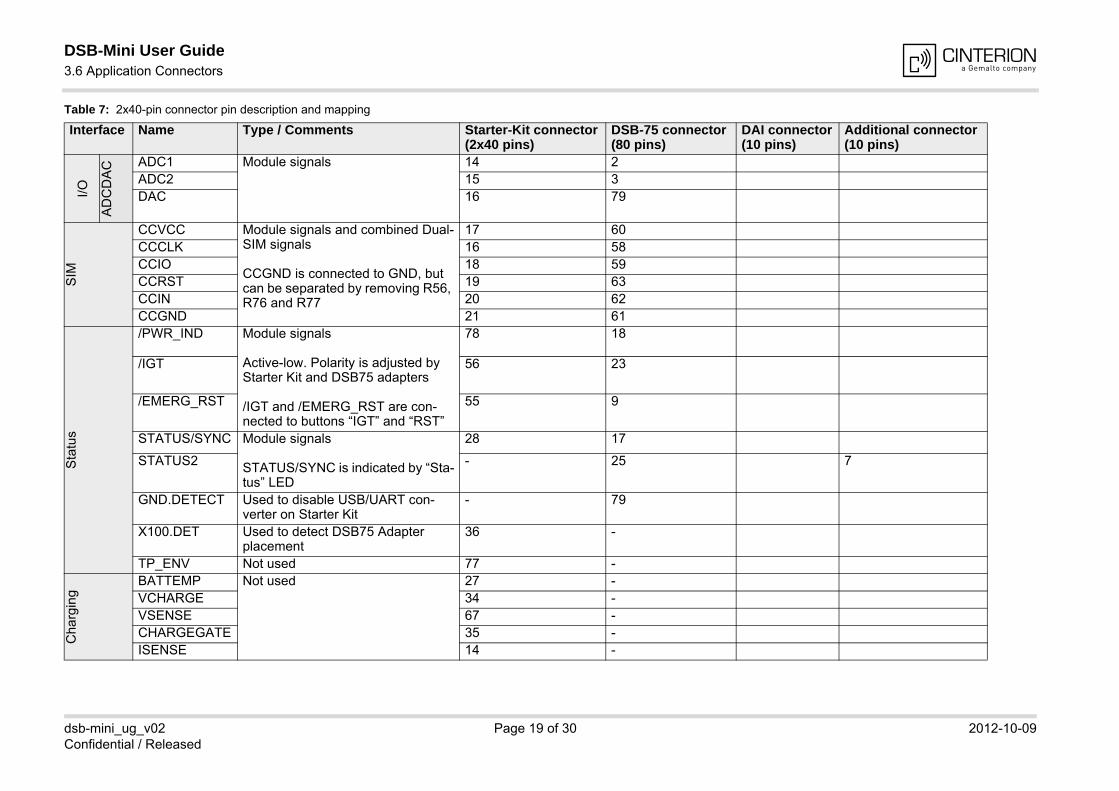
I/O
AD
CD
AC ADC1 Module signals 14 2
ADC2 15 3DAC 16 79
SIM
CCVCC Module signals and combined Dual-SIM signals
CCGND is connected to GND, but can be separated by removing R56, R76 and R77
17 60CCCLK 16 58CCIO 18 59CCRST 19 63CCIN 20 62CCGND 21 61
Sta
tus
/PWR_IND Module signals
Active-low. Polarity is adjusted by Starter Kit and DSB75 adapters
/IGT and /EMERG_RST are con-nected to buttons “IGT” and “RST”
78 18
/IGT 56 23
/EMERG_RST 55 9
STATUS/SYNC Module signals
STATUS/SYNC is indicated by “Sta-tus” LED
28 17
STATUS2 - 25 7
GND.DETECT Used to disable USB/UART con-verter on Starter Kit
- 79
X100.DET Used to detect DSB75 Adapter placement
36 -
TP_ENV Not used 77 -
Cha
rgin
g
BATTEMP Not used 27 -VCHARGE 34 -VSENSE 67 -CHARGEGATE 35 -ISENSE 14 -
Table 7: 2x40-pin connector pin description and mapping
Interface Name Type / Comments Starter-Kit connector(2x40 pins)
DSB-75 connector(80 pins)
DAI connector(10 pins)
Additional connector(10 pins)
DSB-Mini User Guide3.6 Application Connectors23
c
dsb-mini_ug_v02 Page 20 of 30 2012-10-09Confidential / Released
Pow
er
Vo
ltage
do
ma
in
VDDLP Module signals 24 33VEXT1 76 46VEXT2 46 - 5V480 Supply voltage
Supplied from USB power supply (5V), external power supply (8-30V) or from Starter Kit
47 - 1 1
3V Generated from 3V when module is on (/PWR_IND=0)
Indicated by “On/Off” LED
75 - 2 3
Sup
ply
BATT+ Module power supply
Supplied from Battery supply (“BAT” connector) or generated from V480 as selected by switch “BATT+”
41, 80 41-45
GND GND 19-22, 42, 78 1, 4, 37-40, 80 10AGND =GND 43 57N/C Reserved for future use 8 9
Table 7: 2x40-pin connector pin description and mapping
Interface Name Type / Comments Starter-Kit connector(2x40 pins)
DSB-75 connector(80 pins)
DAI connector(10 pins)
Additional connector(10 pins)
DSB-Mini User Guide3.6 Application Connectors23
c
dsb-mini_ug_v02 Page 21 of 30 2012-10-09Confidential / Released
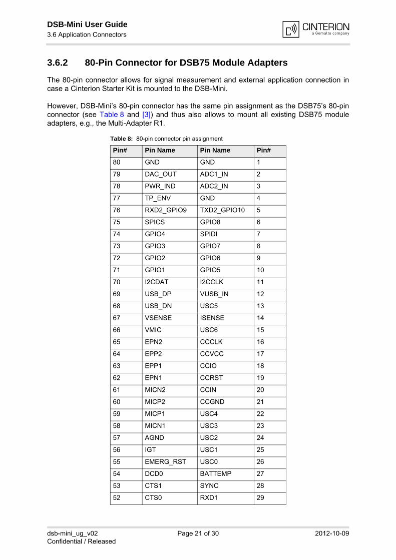
3.6.2 80-Pin Connector for DSB75 Module Adapters
The 80-pin connector allows for signal measurement and external application connection incase a Cinterion Starter Kit is mounted to the DSB-Mini.
However, DSB-Mini’s 80-pin connector has the same pin assignment as the DSB75’s 80-pinconnector (see Table 8 and [3]) and thus also allows to mount all existing DSB75 moduleadapters, e.g., the Multi-Adapter R1.
Table 8: 80-pin connector pin assignment
Pin# Pin Name Pin Name Pin#
80 GND GND 1
79 DAC_OUT ADC1_IN 2
78 PWR_IND ADC2_IN 3
77 TP_ENV GND 4
76 RXD2_GPIO9 TXD2_GPIO10 5
75 SPICS GPIO8 6
74 GPIO4 SPIDI 7
73 GPIO3 GPIO7 8
72 GPIO2 GPIO6 9
71 GPIO1 GPIO5 10
70 I2CDAT I2CCLK 11
69 USB_DP VUSB_IN 12
68 USB_DN USC5 13
67 VSENSE ISENSE 14
66 VMIC USC6 15
65 EPN2 CCCLK 16
64 EPP2 CCVCC 17
63 EPP1 CCIO 18
62 EPN1 CCRST 19
61 MICN2 CCIN 20
60 MICP2 CCGND 21
59 MICP1 USC4 22
58 MICN1 USC3 23
57 AGND USC2 24
56 IGT USC1 25
55 EMERG_RST USC0 26
54 DCD0 BATTEMP 27
53 CTS1 SYNC 28
52 CTS0 RXD1 29
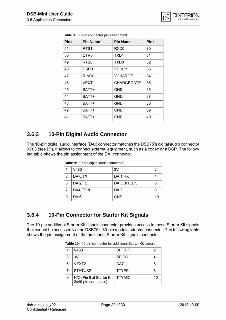
DSB-Mini User Guide3.6 Application Connectors23
c
dsb-mini_ug_v02 Page 22 of 30 2012-10-09Confidential / Released
3.6.3 10-Pin Digital Audio Connector
The 10-pin digital audio interface (DAI) connector matches the DSB75’s digital audio connectorX703 (see [3]). It allows to connect external equipment, such as a codec or a DSP. The follow-ing table shows the pin assignment of the DAI connector.
3.6.4 10-Pin Connector for Starter Kit Signals
The 10-pin additional Starter Kit signals connector provides access to those Starter Kit signalsthat cannot be accessed via the DSB75’s 80-pin module adapter connector. The following tableshows the pin assignment of the additional Starter Kit signals connector.
51 RTS1 RXD0 30
50 DTR0 TXD1 31
49 RTS0 TXD0 32
48 DSR0 VDDLP 33
47 RING0 VCHARGE 34
46 VEXT CHARGEGATE 35
45 BATT+ GND 36
44 BATT+ GND 37
43 BATT+ GND 38
42 BATT+ GND 39
41 BATT+ GND 40
Table 9: 10-pin digital audio connector
1 V480 3V 2
3 DAI0/TX DAI1/RX 4
5 DAI2/FS DAI3/BITCLK 6
7 DA4/FSIN DAI5 8
9 DAI6 GND 10
Table 10: 10-pin connector for additional Starter Kit signals
1 V480 SPICLK 2
3 3V SPIDO 4
5 VEXT2 DA7 6
7 STATUS2 TTYEP 8
9 N/C (Pin 8 of Starter Kit 2x40 pin connector)
TTYMIC 10
Table 8: 80-pin connector pin assignment
Pin# Pin Name Pin Name Pin#
DSB-Mini User Guide3.7 Patch Field23
c
dsb-mini_ug_v02 Page 23 of 30 2012-10-09Confidential / Released
3.7 Patch Field
To realize smallish external applications like for instance measurement circuits, the DSB-Miniprovides a so-called patch field on board, comprising a number of unconnected solder padstogether with GND pads and 3.0V/5V supply pads (see Figure 3).
DSB-Mini User Guide4 Appendix: Schematics and Placement30
c
dsb-mini_ug_v02 Page 24 of 30 2012-10-09Confidential / Released
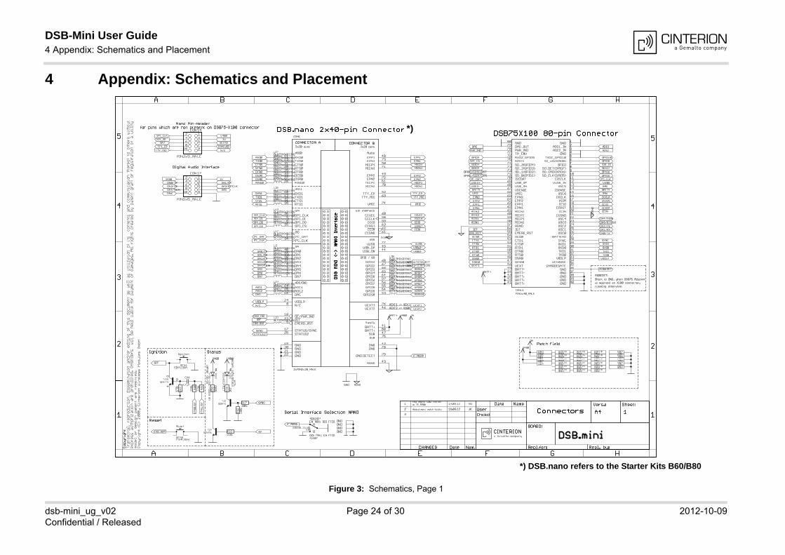
4 Appendix: Schematics and Placement
Figure 3: Schematics, Page 1
*) DSB.nano refers to the Starter Kits B60/B80
*)
DSB-Mini User Guide4 Appendix: Schematics and Placement30
c
dsb-mini_ug_v02 Page 25 of 30 2012-10-09Confidential / Released
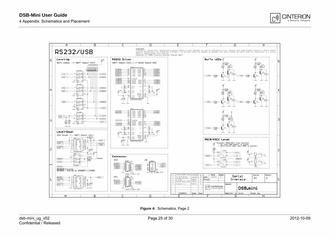
Figure 4: Schematics, Page 2
DSB-Mini User Guide4 Appendix: Schematics and Placement30
c
dsb-mini_ug_v02 Page 26 of 30 2012-10-09Confidential / Released
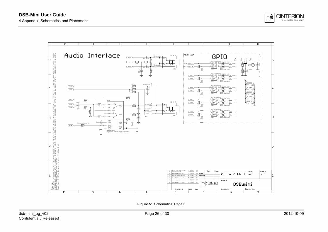
Figure 5: Schematics, Page 3
DSB-Mini User Guide4 Appendix: Schematics and Placement30
c
dsb-mini_ug_v02 Page 27 of 30 2012-10-09Confidential / Released
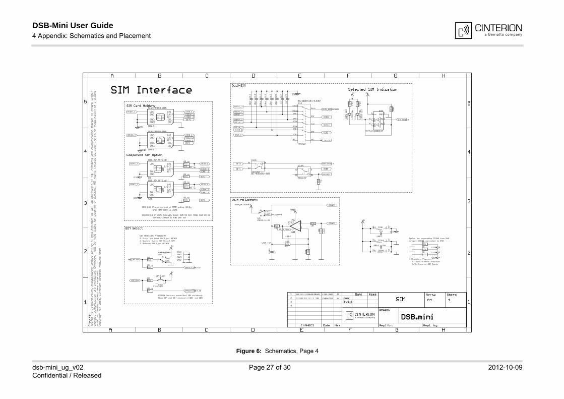
Figure 6: Schematics, Page 4
DSB-Mini User Guide4 Appendix: Schematics and Placement30
c
dsb-mini_ug_v02 Page 28 of 30 2012-10-09Confidential / Released
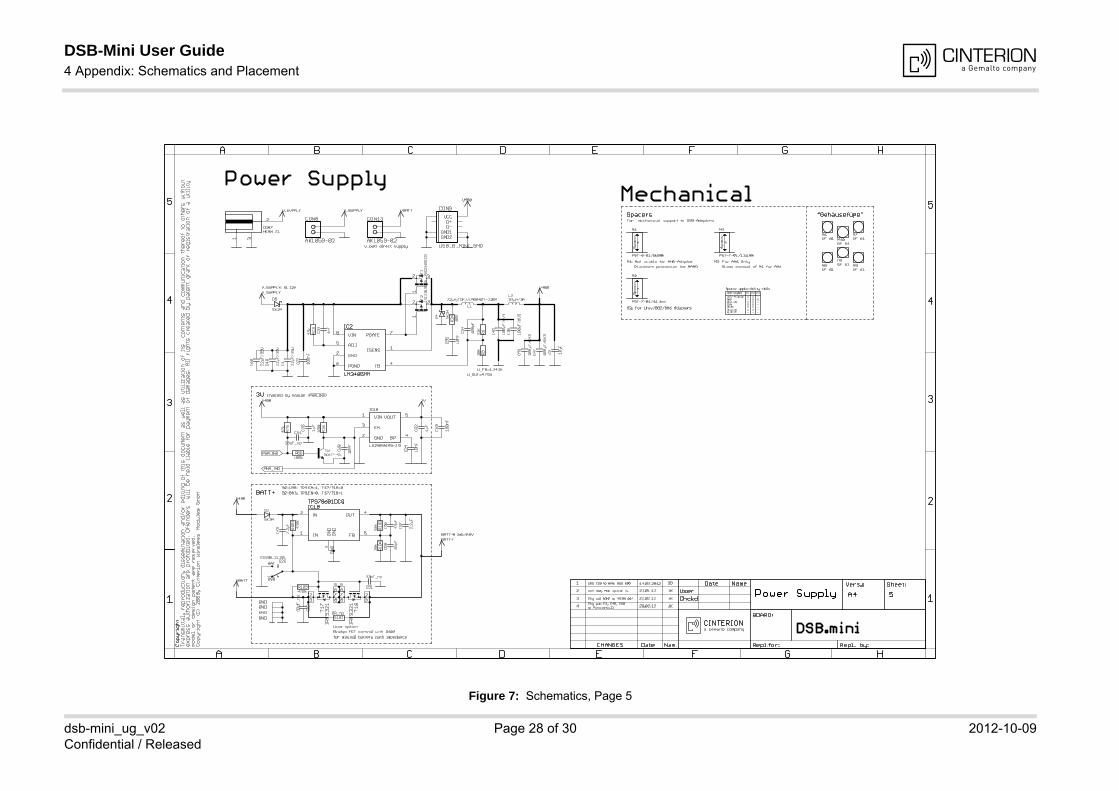
Figure 7: Schematics, Page 5
DSB-Mini User Guide4 Appendix: Schematics and Placement30
c
dsb-mini_ug_v02 Page 29 of 30 2012-10-09Confidential / Released
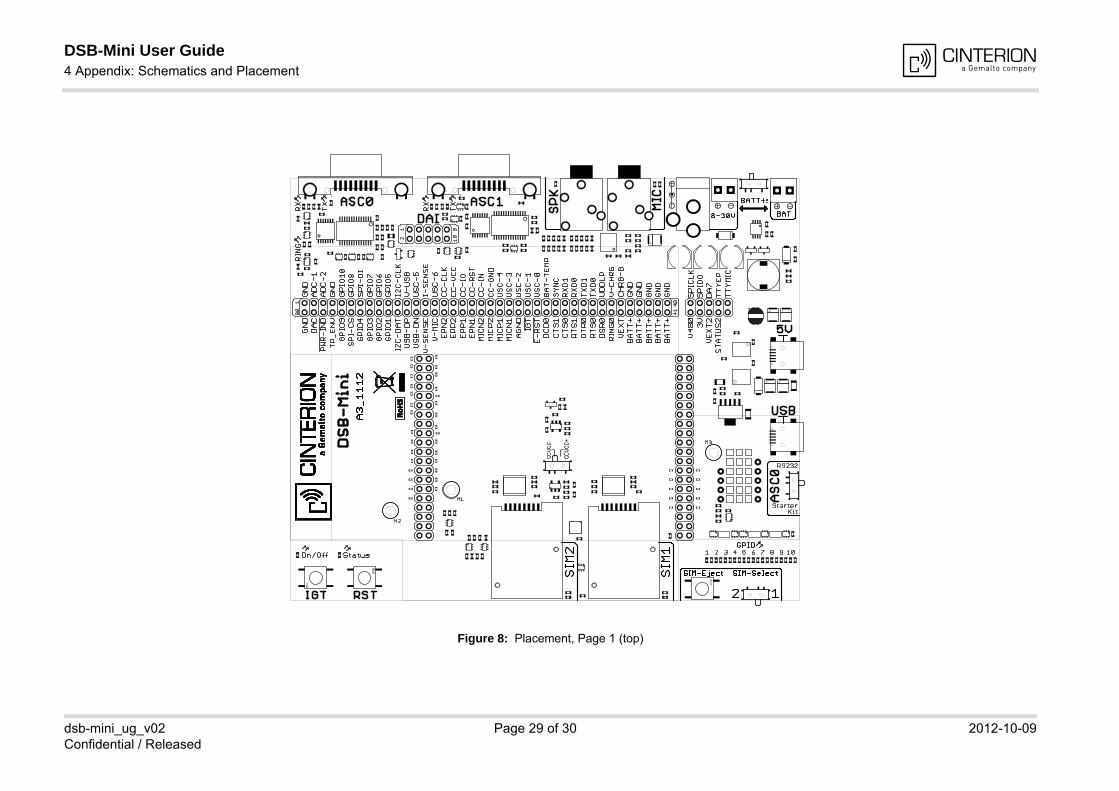
Figure 8: Placement, Page 1 (top)
DSB-Mini User Guide4 Appendix: Schematics and Placement30
c
dsb-mini_ug_v02 Page 30 of 30 2012-10-09Confidential / Released
Figure 9: Placement, Page 2 (with Starter Kit mounted)
R34
R35
R31
R32
R21
R48
R33
R14 R7